

查询ISP1048E供应商查询ISP1048E供应商
• HIGH DENSITY PROGRAMMABLE LOGIC
— 8,000 PLD Gates
— 96 I/O Pins, Twelve Dedicated Inputs
— 288 Registers
— High-Speed Global Interconnects
— Wide Input Gating for Fast Counters, State
Machines, Address Decoders, etc.
— Small Logic Block Size for Random Logic
— Functionally and Pin-out Compatible to ispLSI 1048C
2
• HIGH PERFORMANCE E
—
fmax = 125 MHz Maximum Operating Frequency
tpd = 7.5 ns Propagation Delay
—
— TTL Compatible Inputs and Outputs
— Electrically Eraseable and Reprogrammable
— Non-Volatile
— 100% Tested at Time of Manufacture
• IN-SYSTEM PROGRAMMABLE
— In-System Programmable (ISP™) 5V Only
— Increased Manufacturing Yields, Reduced Time-to-
Market and Improved Product Quality
— Reprogram Soldered Devices for Faster Prototyping
• OFFERS THE EASE OF USE AND FAST SYSTEM
SPEED OF PLDs WITH THE DENSITY AND FLEXIBILITY
OF FIELD PROGRAMMABLE GATE ARRAYS
— Complete Programmable Device Can Combine Glue
Logic and Structured Designs
— Enhanced Pin Locking Capability
— Four Dedicated Clock Input Pins
— Synchronous and Asynchronous Clocks
— Programmable Output Slew Rate Control to
Minimize Switching Noise
— Flexible Pin Placement
— Optimized Global Routing Pool Provides Global
Interconnectivity
• ispLSI DEVELOPMENT TOOLS
ispVHDL™ Systems
— VHDL/Verilog-HDL/Schematic Design Options
— Functional/Timing/VHDL Simulation Options
ispDS+™ VHDL Synthesis-Optimized Logic Fitter
— Supports Leading Third-Party Design Environments
for Schematic Capture, Synthesis and Timing
Simulation
— Static Timing Analyzer
ispDS™ Software
— Lattice HDL or Boolean Logic Entry
— Functional Simulator and Waveform Viewer
ISP Daisy Chain Download Software
CMOS® TECHNOLOGY
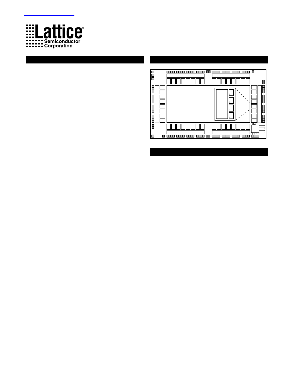
ispLSI® 1048E
High-Density Programmable Logic
Functional Block DiagramFeatures
Output Routing Pool
F7 F6 F5 F4 F3 F2 F1 F0
A0
A1
A2
A3
Global Routing Pool (GRP) GLB
A4
A5
Output Routing Pool
A6
A7
B0 B1 B2 B3 B4 B5 B6 B7
Output Routing Pool
Description
The ispLSI 1048E is a High-Density Programmable Logic
Device containing 288 Registers, 96 Universal I/O pins,
12 Dedicated Input pins, four Dedicated Clock Input pins,
two dedicated Global OE input pins, and a Global Routing
Pool (GRP). The GRP provides complete interconnectivity
between all of these elements. The ispLSI 1048E features 5V in-system programmability and in-system
diagnostic capabilities. The ispLSI 1048E offers nonvolatile reprogrammability of the logic, as well as the
interconnect to provide truly reconfigurable systems. A
functional superset of the ispLSI 1048 architecture, the
ispLSI 1048E device adds two new global output enable
pins and two additional dedicated inputs.
The basic unit of logic on the ispLSI 1048E device is the
Generic Logic Block (GLB). The GLBs are labeled A0,
A1…F7 (see Figure 1). There are a total of 48 GLBs in the
ispLSI 1048E device. Each GLB has 18 inputs, a programmable AND/OR/Exclusive OR array, and four outputs
which can be configured to be either combinatorial or
registered. Inputs to the GLB come from the GRP and
dedicated inputs. All of the GLB outputs are brought back
into the GRP so that they can be connected to the inputs
of any other GLB on the device.
Output Routing Pool
E7 E6 E5 E4 E3 E2 E1 E0
DQ
DQ
Logic
Array
DQ
DQ
C0 C1 C2 C3 C4 C5 C6 C7
Output Routing Pool
D7
D6
D5
D4
D3
D2
Output Routing Pool
D1
D0
CLK
0139G1A-isp
Copyright © 1998 Lattice Semiconductor Corp. All brand or product names are trademarks or registered trademarks of their respective holders. The specifications and information herein are subject
to change without notice.
LATTICE SEMICONDUCTOR CORP., 5555 Northeast Moore Ct., Hillsboro, Oregon 97124, U.S.A. July 1998
Tel. (503) 681-0118; 1-800-LATTICE; FAX (503) 681-3037; http://www.latticesemi.com
1048E_08
1
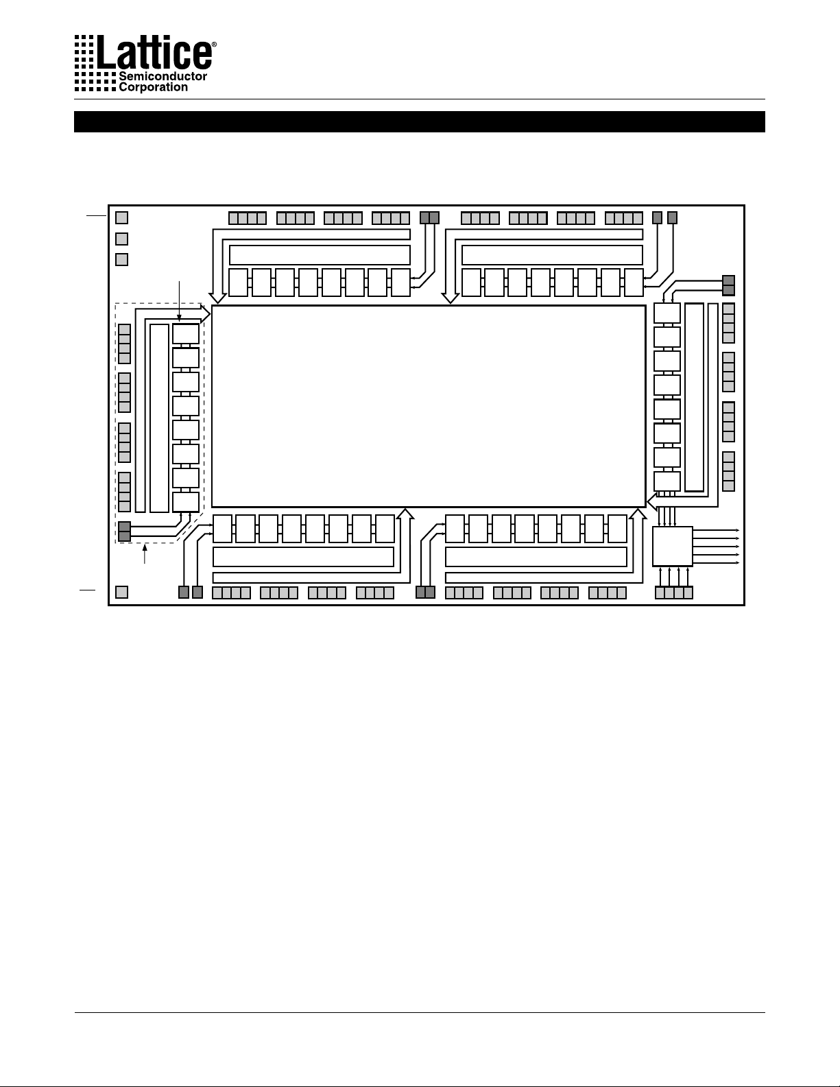
Functional Block Diagram
Figure 1. ispLSI 1048E Functional Block Diagram
Specifications ispLSI 1048E
RESET
GOE 0
GOE 1
I/O 0
I/O 1
I/O 2
I/O 3
I/O 4
I/O 5
I/O 6
I/O 7
I/O 8
I/O 9
I/O 10
I/O 11
I/O 12
I/O 13
I/O 14
I/O 15
SDI/IN 0
MODE/IN 1
ispEN/NC
Generic
Logic Blocks
Input Bus
Output Routing Pool (ORP)
Megablock
(GLBs)
A0
A1
A2
A3
A4
A5
A6
A7
IN 2
I/O94I/O95I/O93I/O92I/O91I/O90I/O89I/O88I/O87I/O86I/O85I/O84I/O83I/O82I/O81I/O
Input Bus
Output Routing Pool (ORP)
F7 F6 F5 F4 F3 F2 F1 F0
B0 B1 B2 B3 B4 B5 B6 B7
Output Routing Pool (ORP)
Input Bus
SDO/
I/O17I/O16I/O18I/O19I/O20I/O21I/O22I/O23I/O24I/O25I/O26I/O27I/O28I/O29I/O30I/O
IN 3
80
Routing
31
IN
IN
11
10
I/O78I/O79I/O77I/O76I/O75I/O74I/O73I/O72I/O71I/O70I/O69I/O68I/O67I/O66I/O65I/O
Output Routing Pool (ORP)
E7 E6 E5 E4 E3 E2 E1 E0
Global
Pool
(GRP)
C0 C1 C2 C3 C4 C5 C6 C7
Output Routing Pool (ORP)
Input Bus
I/O33I/O32I/O34I/O35I/O36I/O37I/O38I/O39I/O40I/O41I/O42I/O43I/O44I/O45I/O46I/O
SCLK/
IN 5IN4
Input Bus
IN
IN
9
64
8
IN 7
IN 6
lnput Bus
I/O 63
I/O 62
I/O 61
I/O 60
I/O 59
I/O 58
I/O 57
I/O 56
I/O 55
I/O 54
I/O 53
I/O 52
I/O 51
I/O 50
I/O 49
I/O 48
D7
D6
D5
D4
D3
D2
Output Routing Pool (ORP)
D1
D0
CLK 0
CLK 1
Clock
Network
Y0Y1Y2Y
CLK 2
IOCLK 0
IOCLK 1
0139F(2)-48B-isp
3
Distribution
47
The device also has 96 I/O cells, each of which is directly
connected to an I/O pin. Each I/O cell can be individually
programmed to be a combinatorial input, registered input, latched input, output or bi-directional
I/O pin with 3-state control. The signal levels are TTL
compatible voltages and the output drivers can source 4
mA or sink 8 mA. Each output can be programmed
independently for fast or slow output slew rate to minimize overall output switching noise.
Eight GLBs, 16 I/O cells, two dedicated inputs and one
ORP are connected together to make a Megablock (see
figure 1). The outputs of the eight GLBs are connected to
a set of 16 universal I/O cells by the ORP. Each ispLSI
1048E device contains six Megablocks.
The GRP has, as its inputs, the outputs from all of the
GLBs and all of the inputs from the bi-directional I/O cells.
All of these signals are made available to the inputs of the
GLBs. Delays through the GRP have been equalized to
minimize timing skew.
Clocks in the ispLSI 1048E device are selected using the
Clock Distribution Network. Four dedicated clock pins
(Y0, Y1, Y2 and Y3) are brought into the distribution
network, and five clock outputs (CLK 0, CLK 1, CLK 2,
IOCLK 0 and IOCLK 1) are provided to route clocks to the
GLBs and I/O cells. The Clock Distribution Network can
also be driven from a special clock GLB (D0). The logic
of this GLB allows the user to create an internal clock
from a combination of internal signals within the device.
2
Specifications ispLSI 1048E
Absolute Maximum Ratings
1
Supply Voltage Vcc. ................................. -0.5 to +7.0V
Input Voltage Applied........................-2.5 to VCC +1.0V
Off-State Output Voltage Applied .....-2.5 to VCC +1.0V
Storage Temperature................................ -65 to 150°C
Case Temp. with Power Applied .............. -55 to 125°C
Max. Junction Temp. (TJ) with Power Applied ... 150°C
1. Stresses above those listed under the “Absolute Maximum Ratings” may cause permanent damage to the device. Functional
operation of the device at these or at any other conditions above those indicated in the operational sections of this specification
is not implied (while programming, follow the programming specifications).
DC Recommended Operating Conditions
V
V
V
CC
IL
IH
SYMBOL
Supply Voltage
Input Low Voltage
Input High Voltage
PARAMETER
Commercial
Industrial
TA = 0°C to + 70°C
= -40°C to + 85°C
T
A
MIN. MAX. UNITS
4.75
4.5
0
2.0
5.25
5.5
0.8
V
cc
+1
V
V
V
V
Table 2-0005/1048E
Capacitance (TA=25oC, f=1.0 MHz)
SYMBOL
C
1
C
2
Dedicated Input, I/O, Y1, Y2, Y3, Clock Capacitance
Y0 Clock Capacitance
PARAMETER
Data Retention Specifications
PARAMETER
Data Retention
Erase/Reprogram Cycles
UNITSTYPICAL TEST CONDITIONS
8
15
MINIMUM MAXIMUM UNITS
20
10000
pf
pf
–
–
V = 5.0V, V = 2.0V
CC
V = 5.0V, V = 2.0V
CC PIN
PIN
Table 2-0006/1048E
Years
Cycles
Table 2-0008/1048E
3
Switching Test Conditions
Specifications ispLSI 1048E
Input Pulse Levels
Input Rise and Fall Time
Input Timing Reference Levels
Output Timing Reference Levels
Output Load
3-state levels are measured 0.5V from
steady-state active level.
GND to 3.0V
≤ 3 ns 10% to 90%
1.5V
1.5V
See Figure 2
Table 2-0003/1048E
Output Load Conditions (see Figure 2)
TEST CONDITION R1 R2 CL
A 470Ω 390Ω 35pF
Active High
B
Active Low
Active High to Z
at V -0.5V
C
Active Low to Z
at V +0.5V
OH
OL
∞ 390Ω 35pF
470Ω 390Ω 35pF
∞ 390Ω 5pF
470Ω 390Ω 5pF
Table 2-0004a
Figure 2. Test Load
+ 5V
R
1
Device
Output
R
2
*
CL includes Test Fixture and Probe Capacitance.
*
C
L
Test
Point
0213a
DC Electrical Characteristics
Over Recommended Operating Conditions
–
–
–
–
–
–
–
175
175
3
0.4
–
-10
10
-150
-150
-200
–
–
Table 2-0007/1048E
µA
µA
µA
µA
mA
mA
mA
SYMBOL
V
OL
V
OH
I
IL
I
IH
I
IL-isp
I
IL-PU
1
I
OS
2, 4
I
CC
Output Low Voltage
Output High Voltage
Input or I/O Low Leakage Current
Input or I/O High Leakage Current
ispEN Input Low Leakage Current
I/O Active Pull-Up Current
Output Short Circuit Current
Operating Power Supply Current
PARAMETER
I = 8 mA
OL
I = -4 mA
OH
0V ≤ V ≤ V (Max.)
IN IL
3.5V ≤ V ≤ V
0V ≤ V ≤ V
0V ≤ V ≤ V
V = 5V, V = 0.5V
V = 0.0V, V = 3.0V
f = 1 MHz
CLOCK
IN CC
IN
IN IL
CC OUT
IL
1. One output at a time for a maximum duration of one second. V = 0.5V was selected to avoid test problems
CONDITION MIN. TYP. MAX. UNITS
–
2.4
–
–
IL
–
–
–
IH
Commercial
Industrial
OUT
–
–
by tester ground degradation. Characterized but not 100% tested.
2. Measured using twelve 16-bit counters.
3. Typical values are at V = 5V and T = 25°C.
4. Maximum I varies widely with specific device configuration and operating frequency. Refer to the Power Consumption
CC
CC A
section of this data sheet and Thermal Management section of the Lattice Semiconductor Data Book or CD-ROM to
estimate maximum I .
CC
V
V
4

External Timing Parameters
Over Recommended Operating Conditions
Specifications ispLSI 1048E
PARAMETER
tpd1
tpd2
fmax (Int.)
fmax (Ext.)
fmax (Tog.)
tsu1
tco1
th1
tsu2
tco2
th2
tr1
trw1
tptoeen
tptoedis
tgoeen
tgoedis
4
TEST
COND.
A 1 Data Propagation Delay, 4PT Bypass, ORP Bypass – 10.0 ns
A 2 Data Propagation Delay, Worst Case Path – ns
A 3 Clock Frequency with Internal Feedback 90.9 – MHz
– 4 Clock Frequency with External Feedback – MHz
– 5 Clock Frequency, Max. Toggle – MHz
– 6 GLB Reg. Setup Time before Clock,4 PT Bypass – ns
A 7 GLB Reg. Clock to Output Delay, ORP Bypass – ns
– 8 GLB Reg. Hold Time after Clock, 4 PT Bypass – ns
– 9 GLB Reg. Setup Time before Clock – ns
– 10 GLB Reg. Clock to Output Delay – ns
– 11 GLB Reg. Hold Time after Clock – ns
A 12 Ext. Reset Pin to Output Delay – ns
– 13 Ext. Reset Pulse Duration – ns
B 14 Input to Output Enable – ns
C 15 Input to Output Disable – ns
B 16 Global OE Output Enable – ns9.0
C 17 Global OE Output Disable – ns
2
DESCRIPTION#
1
1
( )
twh + twl
3
1
( )
tsu2 + tco1
twh – 18 External Synchronous Clock Pulse Duration, High 4.0 ns
twl
tsu3
th3
1. Unless noted otherwise, all parameters use a GRP load of 4 GLBs, 20 PTXOR path, ORP and Y0 clock.
2. Refer to Timing Model in this data sheet for further details.
3. Standard 16-bit counter using GRP feedback.
4. Reference Switching Test Conditions section.
– 19 External Synchronous Clock Pulse Duration, Low 4.0 ns
– 20 I/O Reg. Setup Time before Ext. Sync Clock (Y2, Y3) – ns
– 21 I/O Reg. Hold Time after Ext. Sync. Clock (Y2, Y3) – ns
-125
MIN. MAX.
– 7.5
–
10.0
125.0 –
91.0
167.0
–
–
–
5.5
–
4.5
0.0
–
6.5
–
–
5.5
0.0
–
–
10.0
5.0
–
–
12.0
–
12.0
– 7.0
– 7.0 9.0
3.0
–
3.0
–
3.0 –
0.0 –
-100
MIN. MAX.
– 10.0
–
12.5
100.0 –
6.5
–
0.0
7.5
–
0.0
–
6.5
–
–
– 9.0
– 9.0
4.0
4.0
3.5
0.0
–
–
–
6.5
–
–
7.5
–
13.5
–
15.0
15.0
–
–
–
–
71.0
125.0
MIN. MAX.
71.0
125.0
6.5
0.0
7.5
0.0
6.5
USE 1048E-100 FOR
4.0
0.0
-90
12.5
6.5
7.5
13.5
15.0
NEW DESIGNS
15.0
–
–
Table 2-0030A/1048E
UNITS
5

External Timing Parameters
Over Recommended Operating Conditions
Specifications ispLSI 1048E
PARAMETER
tpd1
tpd2
fmax (Int.)
fmax (Ext.)
fmax (Tog.)
tsu1
tco1
th1
tsu2
tco2
th2
tr1
trw1
tptoeen
tptoedis
tgoeen
tgoedis
4
TEST
COND.
A 1 Data Propagation Delay, 4PT Bypass, ORP Bypass – 20.0 ns
A 2 Data Propagation Delay, Worst Case Path – ns
A 3 Clock Frequency with Internal Feedback 50.0 – MHz
– 4 Clock Frequency with External Feedback – MHz
– 5 Clock Frequency, Max. Toggle – MHz
– 6 GLB Reg. Setup Time before Clock,4 PT Bypass – ns
A 7 GLB Reg. Clock to Output Delay, ORP Bypass – ns
– 8 GLB Reg. Hold Time after Clock, 4 PT Bypass – ns
– 9 GLB Reg. Setup Time before Clock – ns
– 10 GLB Reg. Clock to Output Delay – ns
– 11 GLB Reg. Hold Time after Clock – ns
A 12 Ext. Reset Pin to Output Delay – ns
– 13 Ext. Reset Pulse Duration – ns
B 14 Input to Output Enable – ns
C 15 Input to Output Disable – ns
B 16 Global OE Output Enable – ns16.0
C 17 Global OE Output Disable – ns16.0
2
DESCRIPTION#
( )
1
twh + twl
1
3
1
( )
tsu2 + tco1
twh – 18 External Synchronous Clock Pulse Duration, High 6.5 ns
twl
tsu3
th3
1. Unless noted otherwise, all parameters use a GRP load of 4 GLBs, 20 PTXOR path, ORP and Y0 clock.
2. Refer to Timing Model in this data sheet for further details.
3. Standard 16-bit counter using GRP feedback.
4. Reference Switching Test Conditions section.
– 19 External Synchronous Clock Pulse Duration, Low 6.5 ns
– 20 I/O Reg. Setup Time before Ext. Sync Clock (Y2, Y3) – ns
– 21 I/O Reg. Hold Time after Ext. Sync. Clock (Y2, Y3) – ns
-70
MIN. MAX.
– 15.0
–
18.5
70.0 –
9.0
–
0.0
–
0.0
–
15.0
–
18.0
–
18.0
– 12.0
– 12.0
5.0
5.0
4.0
0.0
–
–
–
7.0
–
–
9.0
–
–
–
–
–
–
56.0
100.0
11.0
10.0
-50
MIN. MAX.
24.5
42.0
77.0
12.0
9.5
0.0
14.5
12.0
0.0
20.5
13.0
24.0
NEW DESIGNS
24.0
USE 1048E-70 FOR
–
–
6.5
0.0
Table 2-0030B/1048E
UNITS
6

Specifications ispLSI 1048E
Internal Timing Parameters
2
PARAMETER
Inputs
tiobp
tiolat
tiosu
tioh
tioco
tior
tdin
GRP
tgrp1
tgrp4
tgrp8
tgrp16
tgrp48
GLB
t4ptbpc
t4ptbpr
t1ptxor
t20ptxor
txoradj
tgbp
tgsu
tgh
tgco
tgro
tptre
tptoe
tptck
ORP
torp
torpbp
1. Internal Timing Parameters are not tested and are for reference only.
2. Refer to Timing Model in this data sheet for further details.
3. The XOR adjacent path can only be used by hard macros.
#
22 I/O Register Bypass – – 0.5 ns
23 I/O Latch Delay – – 2.5 ns
24 I/O Register Setup Time before Clock 3.5 4.0 – ns–
25 I/O Register Hold Time after Clock 0.0 -0.5 – ns–
26 I/O Register Clock to Out Delay – – 5.0 ns5.0
27 I/O Register Reset to Out Delay – – 5.0 ns5.0
28 Dedicated Input Delay – – 2.9 ns2.7
29 GRP Delay, 1 GLB Load – – 2.2 ns
30 GRP Delay, 4 GLB Loads – – 2.4 ns
31 GRP Delay, 8 GLB Loads – – 2.7 ns
GRP Delay, 16 GLB Loads – – 3.3 ns
32
33 GRP Delay, 48 GLB Loads – – 5.7 ns
34 4 Product Term Bypass Path Delay (Combinatorial) – – 5.4 ns
35 4 Product Term Bypass Path Delay (Registered) – – 6.3 ns5.3
36 1 Product Term/XOR Path Delay – – 6.5 ns
37 20 Product Term/XOR Path Delay – – 6.5 ns
38 XOR Adjacent Path Delay – – 7.3 ns
39 GLB Register Bypass Delay – – 0.4 ns
40 GLB Register Setup Time before Clock – 0.1 – ns
41 GLB Register Hold Time after Clock – 6.4 – ns
42 GLB Register Clock to Output Delay – – 2.0 ns
43 GLB Register Reset to Output Delay – – 6.3 ns
44 GLB Product Term Reset to Register Delay – – 5.0 ns
45 GLB Product Term Output Enable to I/O Cell Delay – – 5.7 ns
46 GLB Product Term Clock Delay 4.0 5.2 ns
47 ORP Delay – – 1.0 ns
48 ORP Bypass Delay – – 0.0 ns
1
DESCRIPTION
3
-125
MIN. MAX.
0.3
–
1.9
–
3.0 –
0.0 –
– 4.6
– 4.6
– 2.3
1.8
–
–
2.0
–
2.3
–
2.8
–
4.9
–
3.9
– 4.0
–
3.6
–
5.0
–
5.0
–
0.4
–
0.1
–
4.5
–
2.3
–
4.9
–
3.9
–
5.4
2.9 4.0
––1.0
0.0
-100
MIN.
0.5
5.3
3.5 4.7
0.3
2.3
1.9
2.4
2.6
3.0
5.4
5.3
4.6
5.8
6.3
1.0
2.5
6.2
4.5
7.2
1.0
0.0
-90
MIN.MAX. MAX.
UNITS
USE 1048E-100 FOR NEW DESIGNS
Table 2-0036A/1048E
7
Specifications ispLSI 1048E
Internal Timing Parameters
2
PARAMETER
Inputs
tiobp
tiolat
tiosu
tioh
tioco
tior
tdin
GRP
tgrp1
tgrp4
tgrp8
tgrp16
tgrp48
GLB
t4ptbpc
t4ptbpr
t1ptxor
t20ptxor
txoradj
tgbp
tgsu
tgh
tgco
tgro
tptre
tptoe
tptck
ORP
torp
torpbp
1. Internal Timing Parameters are not tested and are for reference only.
2. Refer to Timing Model in this data sheet for further details.
3. The XOR adjacent path can only be used by hard macros.
#
22 I/O Register Bypass – – 0.7 ns
23 I/O Latch Delay – – 4.7 ns
24 I/O Register Setup Time before Clock 4.1 6.5 – ns–
25 I/O Register Hold Time after Clock -0.6 -0.7 – ns–
26 I/O Register Clock to Out Delay – – 7.0 ns6.0
27 I/O Register Reset to Out Delay – – 7.0 ns6.0
28 Dedicated Input Delay – – 6.1 ns4.3
29 GRP Delay, 1 GLB Load – – 5.1 ns
30 GRP Delay, 4 GLB Loads – – 5.4 ns
31 GRP Delay, 8 GLB Loads – – 5.8 ns
GRP Delay, 16 GLB Loads – – 6.6 ns
32
33 GRP Delay, 48 GLB Loads – – 9.8 ns
34 4 Product Term Bypass Path Delay (Combinatorial) – – 10.7 ns
35 4 Product Term Bypass Path Delay (Registered) – – 9.2 ns7.4
36 1 Product Term/XOR Path Delay – – 10.5 ns
37 20 Product Term/XOR Path Delay – – 10.5 ns
38 XOR Adjacent Path Delay – – 11.7 ns
39 GLB Register Bypass Delay – – 2.2 ns
40 GLB Register Setup Time before Clock – 0.0 – ns
41 GLB Register Hold Time after Clock – 11.5 – ns
42 GLB Register Clock to Output Delay – – 3.0 ns
43 GLB Register Reset to Output Delay – – 7.3 ns
44 GLB Product Term Reset to Register Delay – – 7.9 ns
45 GLB Product Term Output Enable to I/O Cell Delay – – 10.0 ns
46 GLB Product Term Clock Delay 6.9 8.3 ns
47 ORP Delay – – 2.5 ns
48 ORP Bypass Delay – – 0.0 ns
1
DESCRIPTION
3
-70
MIN.
0.1
8.5
5.1 6.4
0.6
3.6
3.5
3.7
4.1
4.8
7.5
8.5
8.4
8.4
9.4
1.6
2.0
6.3
6.1
6.8
2.0
0.0
-50
MIN.MAX. MAX.
UNITS
USE 1048E-70 FOR NEW DESIGNS
Table 2-0036B/1048E
8

Specifications ispLSI 1048E
Internal Timing Parameters
PARAMETER
Outputs
t
ob
t
sl
t
oen
t
odis
t
goe
Clocks
t
gy0
t
gy1/2
t
gcp
t
ioy2/3
t
iocp
Global Reset
t
gr
1. Internal timing parameters are not tested and are for reference only.
2. Refer to Timing Model in this data sheet for further details.
#
49 Output Buffer Delay – – 1.7 ns
50 Output Slew Limited Delay Adder – – 12.0 ns10.0
51 I/O Cell OE to Output Enabled – – 6.4 ns
52 I/O Cell OE to Output Disabled – – 6.4 ns5.1
53 Global OE – – 2.6 ns3.9
54 Clock Delay, Y0 to Global GLB Clock Line (Ref. clock) 2.0 2.8 2.8 ns
55 Clock Delay, Y1 or Y2 to Global GLB Clock Line 2.0 2.8 2.8 ns2.0
56 Clock Delay, Clock GLB to Global GLB Clock Line 0.8 0.8 1.8 ns1.8
57 Clock Delay, Y2 or Y3 to I/O Cell Global Clock Line 0.0 0.0 0.5 ns0.0
58 Clock Delay, Clock GLB to I/O Cell Global Clock Line 0.8 0.8 1.8 ns1.8
59 Global Reset to GLB and I/O Registers – – 4.5 ns4.3
1
DESCRIPTION
-125
MIN. MAX.
–
1.3
– 10.0
–
4.3
– 4.3
– 2.7
0.9
0.9
0.9 0.9
0.8 1.8
0.0 0.0
0.8 1.8
– 2.8
MIN.
-100
2.0
5.1
2.0
-90
MIN.MAX. MAX.
UNITS
NEW DESIGNS
USE 1048E-100 FOR
Table 2-0037A/1048E
9
Specifications ispLSI 1048E
Internal Timing Parameters
PARAMETER
Outputs
t
ob
t
sl
t
oen
t
odis
t
goe
Clocks
t
gy0
t
gy1/2
t
gcp
t
ioy2/3
t
iocp
Global Reset
t
gr
1. Internal timing parameters are not tested and are for reference only.
2. Refer to Timing Model in this data sheet for further details.
#
49 Output Buffer Delay – – 3.2 ns
50 Output Slew Limited Delay Adder – – 12.0 ns12.0
51 I/O Cell OE to Output Enabled – – 7.9 ns
52 I/O Cell OE to Output Disabled – – 7.9 ns6.9
53 Global OE – – 8.1 ns5.1
54 Clock Delay, Y0 to Global GLB Clock Line (Ref. clock) 2.8 3.3 3.3 ns
55 Clock Delay, Y1 or Y2 to Global GLB Clock Line 2.8 3.3 3.3 ns2.8
56 Clock Delay, Clock GLB to Global GLB Clock Line 0.8 0.8 1.8 ns1.8
57 Clock Delay, Y2 or Y3 to I/O Cell Global Clock Line 0.1 0.0 0.7 ns0.6
58 Clock Delay, Clock GLB to I/O Cell Global Clock Line 0.8 0.8 1.8 ns1.8
59 Global Reset to GLB and I/O Registers – – 7.5 ns4.5
1
DESCRIPTION
MIN.
-70
2.2
6.9
2.8
-50
MIN.MAX. MAX.
UNITS
NEW DESIGNS
USE 1048E-70 FOR
Table 2-0037B/1048E
10

ispLSI 1048E Timing Model
Specifications ispLSI 1048E
I/O CellORPGLBGRPI/O Cell
Feedback
Ded. In
I/O Pin
(Input)
Reset
Y1,2,3
Y0
GOE 0,1
#59
#28
I/O Reg Bypass
#22
Input
Register
D
RST
Q
#23 - 27
GRP4
#30
GRP Loading
Delay
#29, 31-33
Clock
Distribution
#55 - 58
#54
#53
#34 Comb 4 PT Bypass
Reg 4 PT Bypass
#35
20 PT
XOR Delays
#36 - 38
#59
Control
RE
PTs
OE
CK
#44 - 46
Derivations of tsu, th and tco from the Product Term Clock
3.5 ns
=
Logic + Reg su - Clock (min)
=
(
tiobp + tgrp4 + t20ptxor) + (tgsu) – (tiobp + tgrp4 + tptck(min))
=
(#22 + #30 + #37) + (#40) – (#22 + #30 + #46)
=
(0.3 + 2.0 + 5.0) + (0.1) – (0.3 + 2.0 + 2.9)
=
=
tiobp + tgrp4 + tptck(max)) + (tgh) – (tiobp + tgrp4 + t20ptxor)
(
=
(#22 + #30 + #46) + (#41) - (#22 + #30 + #37)
=
(0.3 + 2.0 + 4.0) + (4.5) – (0.3 + 2.0 + 5.0)
tsu
2.2 ns
th Clock (max) + Reg h - Logic
GLB Reg Bypass ORP Bypass
#39
GLB Reg
Delay
DQ
RST
#40 - 43
1
#48
ORP
Delay
#47
#49, 50
#51, 52
0491
I/O Pin
(Output)
3.4 ns
2.2 ns
9.6 ns
=
Clock (max) + Reg co + Output
=
(
tiobp + tgrp4 + tptck(max)) + (tgco) + (torp + tob)
=
(#22 + #30 + #46) + (#42) + (#47 + #49)
=
(0.3 + 2.0 + 4.0) + (2.3) + (1.0 + 1.3)
1
=
Logic + Reg su - Clock (min)
tiobp + tgrp4 + t20ptxor) + (tgsu) – (tgy0(min) + tgco + tgcp(min))
=
(
(#22 + #30 + #37) + (#40) – (#54 + #42 + #56)
=
(0.3 + 2.0 + 5.0) + (0.1) – (0.9 + 2.3 + 0.8)
=
=
Clock (max) + Reg h - Logic
=
(
tgy0(max) + tgco + tgcp(max)) + (tgh) – (tiobp + tgrp4 + t20ptxor)
=
(#54 + #42 + #56) + (#41) – (#22 + #30 + #37)
=
(0.9 + 2.3 + 1.8) + (4.5) – (0.3 + 2.0 + 5.0)
=
Clock (max) + Reg co + Output
=
(
tgy0(max) + tgco + tgcp(max)) + (tgco) + (torp + tob)
=
(#54 + #42 + #56) + (#42) + (#47 + #49)
=
(0.9 + 2.3 + 1.8) + (2.3) + (1.0 + 1.3)
tco
10.9 ns
Derivations of tsu, th and tco from the Clock GLB
tsu
th
tco
1. Calculations are based upon timing specifications for the ispLSI 1048E-125.
Table 2-0042/1048E
11
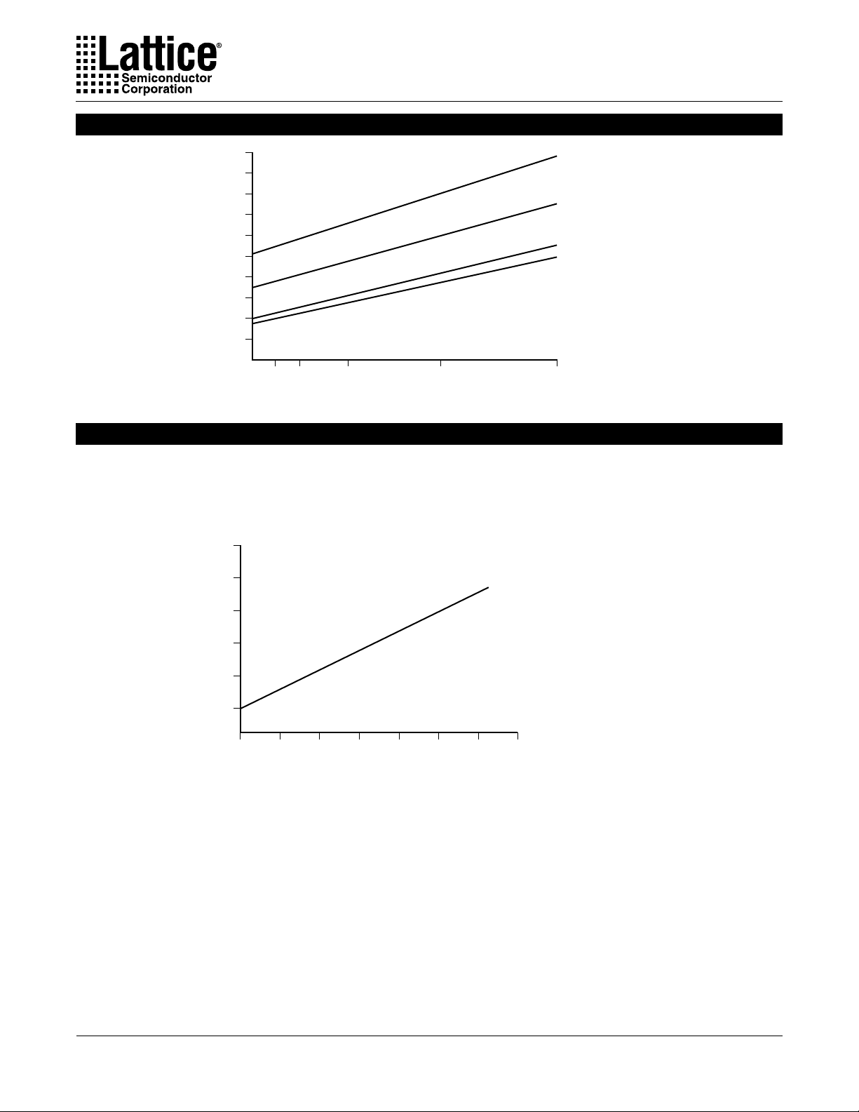
Maximum GRP Delay vs. GLB Loads
Specifications ispLSI 1048E
10
9
8
7
6
5
4
GRP Delay (ns)
3
2
1
1
4
8
16
GLB Loads
Power Consumption
Power Consumption in the ispLSI 1048E device depends
on two primary factors: the speed at which the device is
operating and the number of Product Terms used. Figure
Figure 3. Typical Device Power Consumption vs fmax
380
ispLSI 1048E-50
ispLSI 1048E-70
ispLSI 1048E-90/100
ispLSI 1048E-125
32
48
0127A/1048E
3 shows the relationship between power and operating
speed.
340
300
260
CC (mA)
I
220
180
0 20 40 60 80 100 120 140
ispLSI 1048E
fmax (MHz)
Notes: Configuration of twelve 16-bit counters,
ICC can be estimated for the ispLSI 1048E using the following equation:
ICC = 20 + (# of PTs * 0.42) + (# of nets * Max. freq * 0.010)
Where:
# of PTs = Number of Product Terms used in design
# of nets = Number of Signals used in device
Max. freq = Highest Clock Frequency to the device
The I
average exists. These values are for estimates only. Since the value of I
program in the device, the actual I
estimate is based on typical conditions (VCC = 5.0V, room temperature) and an assumption of 4 GLB loads on
CC
CC
Typical current at 5V, 25°C
should be verified.
is sensitive to operating conditions and the
CC
0127B/1048E
12

Pin Description
Specifications ispLSI 1048E
NAME
I/O 0 - I/O 5
I/O 6 - I/O 11
I/O 12 - I/O 17
I/O 18 - I/O 23
I/O 24 - I/O 29
I/O 30 - I/O 35
I/O 36 - I/O 41
I/O 42 - I/O 47
I/O 48 - I/O 53
I/O 54 - I/O 59
I/O 60 - I/O 65
I/O 66 - I/O 71
I/O 72 - I/O 77
I/O 78 - I/O 83
I/O 84 - I/O 89
I/O 90 - I/O 95
1
PQFP / TQFP PIN NUMBERS DESCRIPTION
21,
22,
23,
24,
27,
28,
35,
41,
53,
59,
67,
73,
86,
92,
99,
105,
118,
124,
3,
9,
29,
36,
42,
54,
60,
68,
74,
87,
93,
100,
106,
119,
125,
4,
10,
34,
40,
52,
58,
66,
72,
85,
91,
98,
104,
117,
123,
2,
8,
64, 114
47, 51
84, 110, 111,IN 6 - IN 11 115, 116, 14
18ispEN/NC
20SDI/IN 0
46MODE/IN 1
50SDO/IN 3
78SCLK/IN 5
30,
37,
43,
55,
61,
69,
75,
88,
94,
101,
107,
120,
126,
5,
11,
25,
31,
38,
44,
56,
62,
70,
76,
89,
95,
102,
108,
121,
127,
6,
12,
Input/Output Pins - These are the general purpose I/O pins used by the
26,
logic array.
32,
39,
45,
57,
63,
71,
77,
90,
96,
103,
109,
122,
128,
7,
13
Global Output Enable input pins.GOE0, GOE1
Dedicated input pins to the device.IN 2, IN 4
Input - Dedicated in-system programming enable input pin. This pin is
brought low to enable the programming mode. When low, the MODE,
SDI, SDO and SCLK controls become active.
Input - This pin performs two functions. When ispEN is logic low, it
functions as an input pin to load programming data into the device.
SDI/IN 0 also is used as one of the two control pins for the ISP state
machine. When ispEN is high, it functions as a dedicated input pin.
Input - This pin performs two functions. When ispEN is logic low, it
functions as pin to control the operation of the isp state machine. When
ispEN is high, it functions as a dedicated input pin.
Output/Input - This pin performs two functions. When ispEN is logic low,
it functions as an output pin to read serial shift register data. When
ispEN is high, it functions as a dedicated input pin.
Input - This pin performs two functions. When ispEN is logic low, it
functions as a clock pin for the Serial Shift Register. When ispEN is
high, it functions as a dedicated input pin.
19RESET
15Y0
83Y1
80Y2
79Y3
1,
17,
GND
VCC
1. NC pins are not to be connected to any active signals, VCC or GND.
97,
16, 48, 82, 113
33, 49, 65, 81,
112
Active Low (0) Reset pin which resets all of the GLB and I/O registers in
the device.
Dedicated Clock input. This clock input is connected to one of the clock
inputs of all of the GLBs on the device.
Dedicated Clock input. This clock input is brought into the clock
distribution network, and can optionally be routed to any GLB on the
device.
Dedicated Clock input. This clock input is brought into the clock
distribution network, and can optionally be routed to any GLB and/or
any I/O cell on the device.
Dedicated Clock input. This clock input is brought into the clock
distribution network, and can optionally be routed to any I/O cell on the
device.
Ground (GND)
V
CC
Table 2 - 0002C-48E
13

Pin Configuration
ispLSI 1048E 128-Pin PQFP Pinout Diagram
Specifications ispLSI 1048E
GND
I/O 84
I/O 85
I/O 86
I/O 87
I/O 88
I/O 89
I/O 90
I/O 91
I/O 92
I/O 93
I/O 94
I/O 95
IN 11
VCC
GND
1
ispEN/NC
RESET
SDI/IN 0
I/O 0
I/O 1
I/O 2
I/O 3
I/O 4
I/O 5
I/O 6
I/O 7
I/O 8
I/O 9
I/O 10
I/O 11
Y0
1
2
3
4
5
6
7
8
9
10
11
12
13
14
15
16
17
18
19
20
21
22
23
24
25
26
27
28
29
30
31
32
I/O 83
I/O 82
128
127
I/O 81
I/O 80
126
125
I/O 79
I/O 78
124
123
I/O 77
I/O 76
121
122
I/O 72
IN 10
117
116
IN 9
115
GOE 1
VCC
114
I/O 75
I/O 74
120
119
I/O 73
118
ispLSI 1048E
Top View
113
IN 8
GND
112
111
IN 7
110
I/O 71
I/O 70
109
108
I/O 69
I/O 68
107
106
I/O 67
I/O 66
105
104
I/O 65
I/O 64
103
102
I/O 63
I/O 62
101
100
I/O 61
I/O 60
99989764
GND
96
95
94
93
92
91
90
89
88
87
86
85
84
83
82
81
80
79
78
77
76
75
74
73
72
71
70
69
68
67
66
65
I/O 59
I/O 58
I/O 57
I/O 56
I/O 55
I/O 54
I/O 53
I/O 52
I/O 51
I/O 50
I/O 49
I/O 48
IN 6
Y1
VCC
GND
Y2
Y3
SCLK/IN 5
I/O 47
I/O 46
I/O 45
I/O 44
I/O 43
I/O 42
I/O 41
I/O 40
I/O 39
I/O 38
I/O 37
I/O 36
GND
33343536373839404142434445464748495051525354555657585960616263
GND
I/O 12
I/O 13
I/O 14
I/O 15
I/O 16
I/O 17
I/O 18
I/O 19
I/O 20
I/O 21
1. NC pins are not to be connected to any active signals, Vcc or GND.
I/O 22
I/O 23
IN 2
MODE/IN 1
VCC
GND
IN 4
I/O 24
I/O 25
SDO/IN 3
I/O 26
I/O 27
I/O 28
I/O 29
14
I/O 30
I/O 31
I/O 32
I/O 33
I/O 34
I/O 35
GOE 0
0124-48C

Pin Configuration
ispLSI 1048E 128-Pin TQFP Pinout Diagram
I/O 83
I/O 82
I/O 81
I/O 80
I/O 79
I/O 78
I/O 77
I/O 76
I/O 75
I/O 74
I/O 73
I/O 72
IN 10
IN 9
VCC
GOE 1
Specifications ispLSI 1048E
IN 8
IN 7
I/O 71
I/O 70
I/O 69
I/O 68
I/O 67
I/O 66
I/O 65
I/O 64
I/O 63
I/O 62
I/O 61
I/O 60
GND
GND
GND
I/O 84
I/O 85
I/O 86
I/O 87
I/O 88
I/O 89
I/O 90
I/O 91
I/O 92
I/O 93
I/O 94
I/O 95
IN 11
VCC
GND
ispEN
RESET
1
SDI/IN 0
I/O 0
I/O 1
I/O 2
I/O 3
I/O 4
I/O 5
I/O 6
I/O 7
I/O 8
I/O 9
I/O 10
I/O 11
Y0
1
2
3
4
5
6
7
8
9
10
11
12
13
14
15
16
17
18
19
20
21
22
23
24
25
26
27
28
29
30
31
32
128
127
126
125
124
123
122
121
120
119
118
117
116
115
ispLSI 1048E
Top View
114
113
112
111
110
109
108
107
106
105
104
103
102
101
99989764
100
96
95
94
93
92
91
90
89
88
87
86
85
84
83
82
81
80
79
78
77
76
75
74
73
72
71
70
69
68
67
66
65
I/O 59
I/O 58
I/O 57
I/O 56
I/O 55
I/O 54
I/O 53
I/O 52
I/O 51
I/O 50
I/O 49
I/O 48
IN 6
Y1
VCC
GND
Y2
Y3
SCLK/IN 5
I/O 47
I/O 46
I/O 45
I/O 44
I/O 43
I/O 42
I/O 41
I/O 40
I/O 39
I/O 38
I/O 37
I/O 36
GND
1
33343536373839404142434445464748495051525354555657585960616263
GND
I/O 12
I/O 13
I/O 14
I/O 15
I/O 16
I/O 17
I/O 18
I/O 19
I/O 20
I/O 21
1. Pins have dual function capability.
I/O 22
I/O 23
IN 2
VCC
GND
MODE/IN 1
1
15
IN 4
I/O 24
SDO/IN 3
1
I/O 25
I/O 26
I/O 27
I/O 28
I/O 29
I/O 30
I/O 31
I/O 32
I/O 33
I/O 34
I/O 35
GOE 0
0124-48/TQFP

Package Thermal Characteristics
For the ispLSI 1048E-125LT, it is strongly recommended
that the actual Icc be verified to ensure that the maximum
junction temperature (TJ) with power supplied is not
exceeded. Depending on the specific logic design and
clock speed, airflow may be required to satisfy the maxi-
Part Number Description
Specifications ispLSI 1048E
mum allowable junction temperature (TJ) specification.
Please refer to the Thermal Management section of the
Lattice Semiconductor Data Book or CD-ROM for additional information on calculating TJ.
ispLSI
1048E XXX X X X
Device Family
Device Number
Speed
125 = 125 MHz fmax
100 = 100 MHz fmax
90 = 90 MHz fmax
70 = 70 MHz fmax
50 = 50 MHz fmax
ispLSI 1048E Ordering Information
FAMILY fmax (MHz)
125
125
100
100 128-Pin TQFP10 ispLSI 1048E-100LT
ispLSI
*Recommend 1048E-100 for new 1048E-90 designs.
**Recommend 1048E-70 for new 1048E-50 designs.
FAMILY fmax (MHz) ORDERING NUMBER PACKAGEtpd (ns)
ispLSI
**Recommend 1048E-70 for new 1048E-50 designs.
90
90
70
70 128-Pin TQFP15 ispLSI 1048E-70LT
50
50
70 128-Pin PQFP15 ispLSI 1048E-70LQI
50 128-Pin PQFP20 ispLSI 1048E-50LQI**
tpd (ns)
7.5
7.5
10
10
10
15
20
–
Grade
Blank = Commercial
I = Industrial
Package
Q = PQFP
T = TQFP
Power
L = Low
COMMERCIAL
ORDERING NUMBER PACKAGE
ispLSI 1048E-125LQ
ispLSI 1048E-125LT
ispLSI 1048E-90LQ*
ispLSI 1048E-90LT*
ispLSI 1048E-50LQ**
INDUSTRIAL
0212/1048E
128-Pin PQFP
128-Pin TQFP
128-Pin PQFPispLSI 1048E-100LQ
128-Pin PQFP
128-Pin TQFP
128-Pin PQFPispLSI 1048E-70LQ
128-Pin PQFP20
128-Pin TQFPispLSI 1048E-50LT**
Table 2-0041A/1048E
Table 2-0041B/1048E
16
 Loading...