

• HIGH DENSITY PROGRAMMABLE LOGIC
Output Routing Pool
B0 B1 B2 B3 B4 B5 B6 B7
A0
A1
A2
A3
A4
A5
A6
A7
C7
C6
C5
C4
C3
C2
C1
C0
Output Routing Pool
Output Routing Pool
CLK
Global Routing Pool (GRP)
0139/1024EA
Logic
Array
DQ
DQ
DQ
DQ
GLB
— 4000 PLD Gates
— 48 I/O Pins, Two Dedicated Inputs
— 144 Registers
— High Speed Global Interconnect
— Wide Input Gating for Fast Counters, State
Machines, Address Decoders, etc.
— Small Logic Block Size for Random Logic
• NEW FEATURES
— 100% IEEE 1149.1 Boundary Scan Testable
— ispJTAG™ In-System Programmable via IEEE 1149.1
(JTAG) Test Access Port
— User Selectable 3.3V or 5V I/O Supports Mixed-
Voltage Systems (V
— Open-Drain Output Option
• HIGH PERFORMANCE E
— fmax = 200 MHz Maximum Operating Frequency
—
tpd = 4.5 ns Propagation Delay
— TTL Compatible Inputs and Outputs
— Electrically Erasable and Reprogrammable
— Non-Volatile
— 100% Tested at Time of Manufacture
— Unused Product Term Shutdown Saves Power
• IN-SYSTEM PROGRAMMABLE
— Increased Manufacturing Yields, Reduced Time-to-
Market and Improved Product Quality
— Reprogram Soldered Devices for Faster Prototyping
• OFFERS THE EASE OF USE AND FAST SYSTEM
SPEED OF PLDs WITH THE DENSITY AND FLEXIBILITY
OF FIELD PROGRAMMABLE GATE ARRAYS
— Complete Programmable Device Can Combine Glue
Logic and Structured Designs
— Enhanced Pin Locking Capability
— Four Dedicated Clock Input Pins
— Synchronous and Asynchronous Clocks
— Programmable Output Slew Rate Control to
Minimize Switching Noise
— Flexible Pin Placement
— Optimized Global Routing Pool Provides Global
Interconnectivity
• ispDesignEXPERT™ – LOGIC COMPILER AND COMPLETE ISP DEVICE DESIGN SYSTEMS FROM HDL
SYNTHESIS THROUGH IN-SYSTEM PROGRAMMING
— Superior Quality of Results
— Tightly Integrated with Leading CAE Vendor Tools
— Productivity Enhancing Timing Analyzer, Explore
Tools, Timing Simulator and ispANALYZER™
— PC and UNIX Platforms
Copyright © 2000 Lattice Semiconductor Corp. All brand or product names are trademarks or registered trademarks of their respective holders. The specifications and information herein are subject
to change without notice.
LATTICE SEMICONDUCTOR CORP., 5555 Northeast Moore Ct., Hillsboro, Oregon 97124, U.S.A. June 2000
Tel. (503) 268-8000; 1-800-LATTICE; FAX (503) 268-8556; http://www.latticesemi.com
1024ea_01 1
CCIO Pin)
2
CMOS® TECHNOLOGY
ispLSI® 1024EA
In-System Programmable High Density PLD
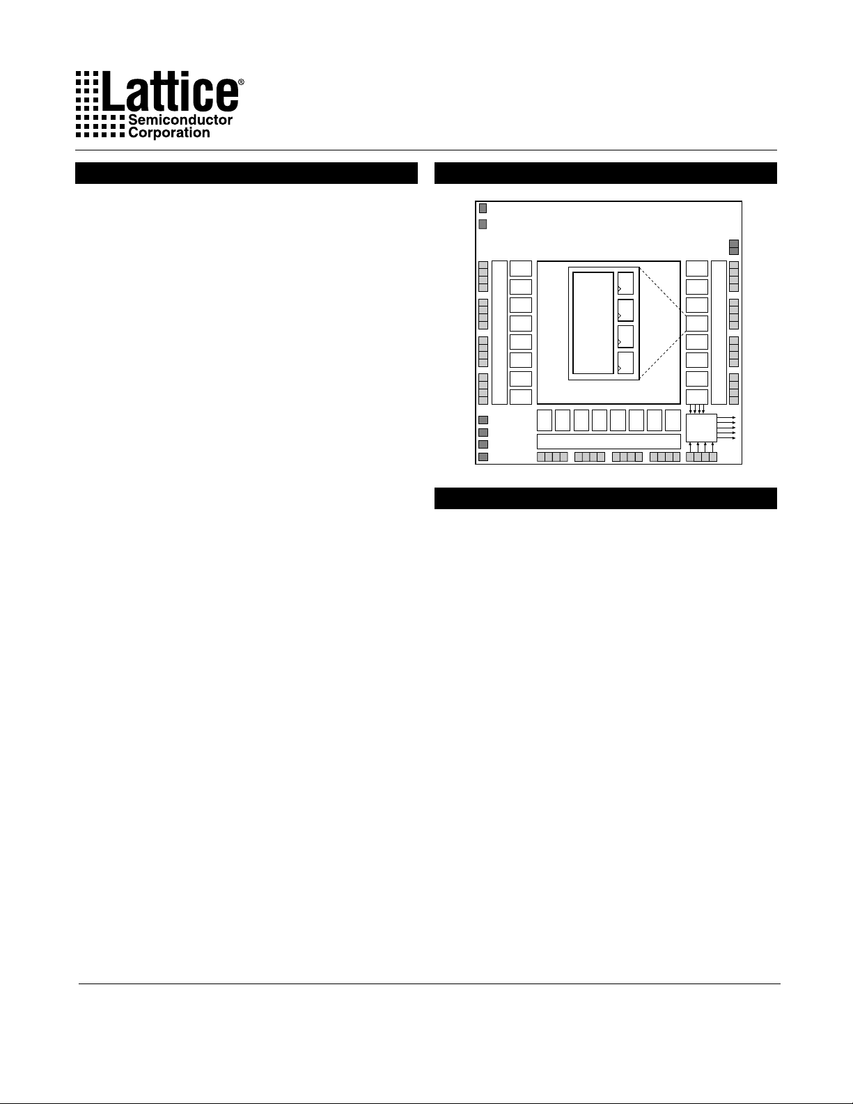
Functional Block DiagramFeatures
Description
The ispLSI 1024EA is a High Density Programmable
Logic Device containing 144 Registers, 48 Universal I/O
pins, two Dedicated Input pins, four Dedicated Clock
Input pins and a Global Routing Pool (GRP). The GRP
provides complete interconnectivity between all of these
elements. The ispLSI 1024EA features 5V in-system
diagnostic capabilities via IEEE 1149.1 Test Access Port.
The ispLSI 1024EA device offers non-volatile
reprogrammability of the logic, as well as the interconnects to provide truly reconfigurable systems. A functional
superset of the ispLSI 1024 architecture, the ispLSI
1024EA device adds user selectable 3.3V or 5V I/O and
open-drain output options.
The basic unit of logic on the ispLSI 1024EA device is the
Generic Logic Block (GLB). The GLBs are labeled A0,
A1…D7 (Figure 1). There are a total of 24 GLBs in the
ispLSI 1024EA device. Each GLB has 18 inputs, a
programmable AND/OR/Exclusive OR array, and four
outputs which can be configured to be either combinatorial or registered. Inputs to the GLB come from the GRP
and dedicated inputs. All of the GLB outputs are brought
back into the GRP so that they can be connected to the
inputs of any other GLB on the device.
Functional Block Diagram
Figure 1. ispLSI 1024EA Functional Block Diagram
RESET
VCCIO
Generic
Logic Blocks
(GLBs)
I/O 0
I/O 1
I/O 2
I/O 3
I/O 4
I/O 5
I/O 6
I/O 7
I/O 8
I/O 9
I/O 10
I/O 11
I/O 12
I/O 13
I/O 14
I/O 15
TDO
TMS
TCK
TDI
Megablock
A0
A1
A2
A3
A4
lnput Bus
A5
Output Routing Pool (ORP)
A6
A7
B0 B1 B2 B3 B4 B5 B6 B7
Output Routing Pool (ORP)
Input Bus
I/O 16
I/O 17
I/O 18
I/O 19
I/O 20
I/O 21
I/O 22
Specifications ispLSI 1024EA
GOE 1/IN 5
GOE 0/IN 4
lnput Bus
I/O 47
I/O 46
I/O 45
I/O 44
I/O 43
I/O 42
I/O 41
I/O 40
I/O 39
I/O 38
I/O 37
I/O 36
I/O 35
I/O 34
I/O 33
I/O 32
Global
Routing
Pool
(GRP)
I/O 23
I/O 24
I/O 25
I/O 26
I/O 27
I/O 28
I/O 29
I/O 30
I/O 31
C7
C6
C5
C4
C3
C2
Output Routing Pool (ORP)
C1
C0
CLK 0
CLK 1
Clock
Network
Y0Y1Y2
CLK 2
IOCLK 0
IOCLK 1
0139B/1024EA
Y3
Distribution
The device also has 48 I/O cells, each of which is directly
connected to an I/O pin. Each I/O cell can be individually
programmed to be a combinatorial input, registered input, latched input, output or bi-directional
I/O pin with 3-state control. The signal levels are TTL
compatible voltages and the output drivers can source 4
mA or sink 8 mA. Each output can be programmed
independently for fast or slow output slew rate to minimize overall output switching noise. By connecting the
VCCIO pin to a common 5V or 3.3V power supply, I/O
output levels can be matched to 5V or 3.3V-compatible
voltages.
Eight GLBs, 16 I/O cells, dedicated inputs (if available)
and one ORP are connected together to make a
Megablock (Figure 1). The outputs of the eight GLBs are
connected to a set of 16 universal I/O cells by the ORP.
Each ispLSI 1024EA device contains three Megablocks.
The GRP has, as its inputs, the outputs from all of the
GLBs and all of the inputs from the bi-directional I/O cells.
All of these signals are made available to the inputs of the
GLBs. Delays through the GRP have been equalized to
minimize timing skew.
Clocks in the ispLSI 1024EA device are selected using
the Clock Distribution Network. Four dedicated clock pins
(Y0, Y1, Y2 and Y3) are brought into the distribution
network, and five clock outputs (CLK 0, CLK 1, CLK 2,
IOCLK 0 and IOCLK 1) are provided to route clocks to the
GLBs and I/O cells. The Clock Distribution Network can
also be driven from a special clock GLB (C0 on the ispLSI
1024EA device). The logic of this GLB allows the user to
create an internal clock from a combination of internal
signals within the device.
Programmable Open-Drain Outputs
In addition to the standard output configuration, the
outputs of the ispLSI 1024EA are individually programmable, either as a standard totem-pole output or an
open-drain output. The totem-pole output drives the
specified Voh and Vol levels, whereas the open-drain
output drives only the specified Vol. The Voh level on the
open-drain output depends on the external loading and
pull-up. This output configuration is controlled by a programmable fuse. The default configuration when the
device is in bulk erased state is totem-pole configuration.
The open-drain/totem-pole option is selectable through
the ispDesignEXPERT software tools.
2
Specifications ispLSI 1024EA
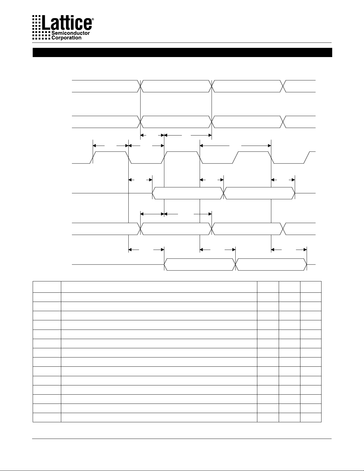
Boundary Scan
Figure 2. Boundary Scan Waveforms and Timing Specifications
TMS
TDI
TCK
TDO
Data to be
captured
Data to be
driven out
T
btch
T
T
btvo
T
T
btcl
T
btcpsu
btuov
btsu
Data Captured
T
bth
T
btcp
T
btco
Valid Data Valid Data
T
btcph
T
btuco
Valid Data Valid Data
T
btoz
T
btuoz
Symbol Parameter Min Max Units
t
btcp
t
btch
t
btcl
t
btsu
t
bth
t
rf
t
btco
t
btoz
t
btvo
t
btcpsu
t
btcph
t
btuco
t
btuoz
t
btuov
TCK [BSCAN test] clock pulse width 100 – ns
TCK [BSCAN test] pulse width high 50 – ns
TCK [BSCAN test] pulse width low 50 – ns
TCK [BSCAN test] setup time 20 – ns
TCK [BSCAN test] hold time 25 – ns
TCK [BSCAN test] rise and fall time 50 – mV/ns
TAP controller falling edge of clock to valid output – 25 ns
TAP controller falling edge of clock to data output disable – 25 ns
TAP controller falling edge of clock to data output enable – 25 ns
BSCAN test Capture register setup time 40 – ns
BSCAN test Capture register hold time 25 – ns
BSCAN test Update reg, falling edge of clock to valid output – 50 ns
BSCAN test Update reg, falling edge of clock to output disable – 50 ns
BSCAN test Update reg, falling edge of clock to output enable – 50 ns
3
Specifications ispLSI 1024EA
Absolute Maximum Ratings
1
Supply Voltage Vcc.................................. -0.5 to +7.0V
Input Voltage Applied........................-2.5 to VCC +1.0V
Off-State Output Voltage Applied .....-2.5 to VCC +1.0V
Storage Temperature................................ -65 to 150°C
Case Temp. with Power Applied .............. -55 to 125°C
Max. Junction Temp. (T
1. Stresses above those listed under the “Absolute Maximum Ratings” may cause permanent damage to the device. Functional
operation of the device at these or at any other conditions above those indicated in the operational sections of this specification
is not implied (while programming, follow the programming specifications).
) with Power Applied ... 150°C
J
DC Recommended Operating Conditions
SYMBOL
VCC
VCCIO
VIL
VIH
PARAMETER
Supply Voltage
Supply Voltage: Output Drivers
Input Low Voltage
Input High Voltage
Commercial
5V
3.3V
TA = 0°C to + 70°C
MIN. MAX. UNITS
4.75
4.75
3.0
0
2.0
5.25
5.25
3.6
0.8
+1
V
cc
Table 2-0005/1024EA
V
V
V
V
V
Capacitance (TA=25oC, f=1.0 MHz)
SYMBOL
C
1
C
2
(Commercial/Industrial)
Y0 Clock Capacitance
PARAMETER
Erase/Reprogram Specifications
PARAMETER
Erase/Reprogram Cycles
UNITSTYPICAL TEST CONDITIONS
8Dedicated Input, I/O, Y1, Y2, Y3, Clock Capacitance
10
MINIMUM MAXIMUM UNITS
10000 — Cycles
pf
pf
V = 5.0V, V = 2.0V
CC
V = 5.0V, V = 2.0V
CC PIN
PIN
Table 2-0006/1024EA
Table 2-0008/1024EA
4

Switching Test Conditions
+ 5V
R
1
R
2
C
L
*
Device
Output
Test
Point
*C
L
includes Test Fixture and Probe Capacitance.
0213a
Specifications ispLSI 1024EA
Input Pulse Levels
Input Rise and Fall Time 10% to 90%
Input Timing Reference Levels
Output Timing Reference Levels
Output Load
3-state levels are measured 0.5V from
steady-state active level.
GND to 3.0V
1.5ns
1.5V
1.5V
See Figure 3
Table 2-0003/1024EA
Figure 3. Test Load
Output Load Conditions (see Figure 3)
TEST CONDITION R1 R2 CL
A 470Ω 390Ω 35pF
Active High
B
Active Low
Active High to Z
at V -0.5V
C
Active Low to Z
at V +0.5V
OH
OL
∞ 390Ω 35pF
470Ω 390Ω 35pF
∞ 390Ω 5pF
470Ω 390Ω 5pF
Table 2-0004/1024EA
DC Electrical Characteristics
Over Recommended Operating Conditions
SYMBOL
V
OL
V
OH
I
IL
I
IH
I
IL-PU
1
I
OS
2, 4, 5
I
CC
Output Low Voltage
Output High Voltage
Input or I/O Low Leakage Current
Input or I/O High Leakage Current
I/O Active Pull-Up Current
Output Short Circuit Current V
Operating Power Supply Current
PARAMETER
I
= 8 mA
OL
I
= -2 mA, V
OH
I
= -4 mA, V
OH
0V ≤ V
IN
- 0.2)V ≤ VIN ≤ V
(V
CCIO
V
≤ V
CCIO
0V ≤ V
IN
= 5.0V or 3.3V, V
CCIO
V
= 0.0V, VIH = 3.0V
IL
f
TOGGLE
1. One output at a time for a maximum duration of one second. V
CONDITION MIN. TYP.
= 3.0V
CCIO
= 4.75V
CCIO
≤ VIL (Max.)
CCIO
≤ 5.25V
IN
≤ V
IL
= 0.5V ——-240 mA
OUT
= 1 MHz
= 0.5V was selected to avoid test
OUT
—
2.4 ——V
2.4 ——V
—
—
—
—
— 152 mA—
problems by tester ground degradation. Characterized but not 100% tested.
2. Measured using eight 16-bit counters.
3. Typical values are at V
4. Unused inputs held at 0.0V.
5. Maximum I
Power Consumption section of this data sheet and the Thermal Management section of the Lattice Semiconductor
Data Book CD-ROM to estimate maximum I
varies widely with specific device configuration and operating frequency. Refer to the
CC
= 5V and TA = 25°C.
CC
CC
.
3
—
—
—
—
—
MAX. UNITS
0.4
-10
10
10
-200
Table 2-0007/1024EA
V
µA
µA
µA
µA
5

External Timing Parameters
Over Recommended Operating Conditions
Specifications ispLSI 1024EA
4
PARAMETER
t
pd1
t
pd2
f
max (Int.)
f
max (Ext.)
f
max (Tog.)
t
su1
t
co1
t
h1
t
su2
t
co2
t
h2
t
r1
t
rw1
t
ptoeen
t
ptoedis
t
goeen
t
goedis
t
wh — 18 External Synchronous Clock Pulse Duration, High ns
t
wl
t
su3
t
h3
1. Unless noted otherwise, all parameters use a GRP load of four GLBs, 20 PTXOR path, ORP and Y0 clock.
2. Refer to Timing Model in this data sheet for further details.
3. Standard 16-bit counter using GRP feedback.
4. Reference Switching Test Conditions section.
TEST
COND.
A 1 Data Propagation Delay, 4PT Bypass, ORP Bypass ns
A 2 Data Propagation Delay, Worst Case Path ns
A 3 Clock Frequency with Internal Feedback MHz
— 4 Clock Frequency with External Feedback MHz
— 5 Clock Frequency, Max. Toggle MHz
— 6 GLB Reg. Setup Time before Clock,4 PT Bypass ns
A 7 GLB Reg. Clock to Output Delay, ORP Bypass ns
— 8 GLB Reg. Hold Time after Clock, 4 PT Bypass ns
— 9 GLB Reg. Setup Time before Clock ns
— 10 GLB Reg. Clock to Output Delay ns
— 11 GLB Reg. Hold Time after Clock ns
A 12 Ext. Reset Pin to Output Delay ns
— 13 Ext. Reset Pulse Duration ns
B 14 Input to Output Enable ns
C 15 Input to Output Disable ns
B 16 Global OE Output Enable ns
C 17 Global OE Output Disable ns
— 19 External Synchronous Clock Pulse Duration, Low ns
— 20 I/O Reg. Setup Time before Ext. Sync Clock (Y2, Y3) ns
— 21 I/O Reg. Hold Time after Ext. Sync. Clock (Y2, Y3) ns
2
DESCRIPTION#
1
1
( )
twh + twl
3
1
( )
tsu2 + tco1
-200
MIN. MAX.
— 4.5
—
6.0
200 —
3.0
—
0.0
3.5
—
0.0
—
3.5
—
—
— 4.5
— 4.5
2.0
2.0
3.0
0.0
—
—
—
3.5
—
—
4.0
—
5.5
—
7.0
7.0
—
—
—
—
143
250
-125
MIN. MAX.
— 7.5
—
10.0
125 —
4.5
—
0.0
5.5
—
0.0
—
5.0
—
—
— 7.0
— 7.0
3.0
3.0
3.0
0.0
—
—
—
4.5
—
—
5.5
—
10.0
—
12.0
12.0
—
—
—
—
100
167
-100
MIN. MAX.
— 10.0
—
12.5
100 —
—
77
125
—
—
6.0
6.0
—
—
0.0
—
7.0
7.0
—
—
0.0
13.5
—
6.5
—
15.0
—
15.0
—
— 9.0
— 9.0
—
4.0
—
4.0
3.5
—
0.0
—
Table 2-0030A/1024EA
UNITS
v.2.5
6

Specifications ispLSI 1024EA
Internal Timing Parameters
PARAM.
2
1
Inputs
tiobp
tiolat
tiosu
tioh
tioco
tior
tdin
22 I/O Register Bypass ns
23 I/O Latch Delay ns
24 I/O Register Setup Time before Clock ns
25 I/O Register Hold Time after Clock ns
26 I/O Register Clock to Out Delay ns
27 I/O Register Reset to Out Delay ns
28 Dedicated Input Delay ns
GRP
tgrp1
tgrp4
tgrp8
tgrp16
tgrp24
29 GRP Delay, 1 GLB Load ns
30 GRP Delay, 4 GLB Loads ns
31 GRP Delay, 8 GLB Loads ns
32 GRP Delay, 16 GLB Loads ns
33 ns
GRP Delay, 24 GLB Loads
GLB
t4ptbpc
t4ptbpr
t1ptxor
t20ptxor
txoradj
tgbp
tgsu
tgh
tgco
tgro
tptre
tptoe
tptck
tgfb
34 4 ProductTerm Bypass Path Delay (Combinatorial) ns
35 4 Product Term Bypass Path Delay (Registered) ns
36 1 ProductTerm/XOR Path Delay ns
37 20 Product Term/XOR Path Delay ns
38 XOR Adjacent Path Delay ns
39 GLB Register Bypass Delay
40 GLB Register Setup Time before Clock ns
41 GLB Register Hold Time after Clock ns
42 GLB Register Clock to Output Delay ns
43 GLB Register Reset to Output Delay ns
44 GLB Product Term Reset to Register Delay ns
45 GLB Product Term Output Enable to I/O Cell Delay ns
46 GLB Product Term Clock Delay ns
47 GLB Feedback Delay ns
3
ORP
torp
torpbp
1. Internal Timing Parameters are not tested and are for reference only.
2. Refer to Timing Model in this data sheet for further details.
3. The XOR adjacent path can only be used by hard macros.
48 ORP Delay ns
49 ORP Bypass Delay ns
-200
MIN. MAX.
—
0.3
—
4.0
3.0
—
0.0
—
—
4.0
—
4.0
—
1.1
—
1.3
—
1.5
—
1.7
—
2.1
—
2.5
—
1.7
—
1.8
—
1.9
—
1.9
—
1.9
—
0.6
0.2
—
1.0
—
—
1.4
—
3.8
—
2.5
—
2.1
1.5
2.5
—
0.0
—
0.8
—
0.1
-125
MIN. MIN.MAX. MAX.
0.3
—
4.0
—
—
—
—
—
—
—
—
—
—
—
—
—
—
—
—
—
—
—
—
—
—
—
4.6
4.6
1.9
1.7
1.9
2.1
2.5
2.9
3.4
3.1
3.6
3.6
3.6
1.2
—
—
1.4
4.9
3.8
5.7
3.9
1.3
0.2
3.0
0.0
0.3
3.5
2.8
-100
—
0.4
—
4.0
3.4
0.0
1.4
4.0
3.5
—
—
—
5.0
—
5.0
—
2.2
—
2.1
—
2.3
—
2.5
—
2.9
—
3.3
—
4.9
—
3.8
—
4.3
—
4.3
—
4.3
—
2.1
—
—
—
1.7
—
5.0
—
4.5
—
7.2
4.7
—0.3— 0.3
—
1.4
—
0.4
Table 2-0036A/1024EA
UNITSDESCRIPTION#
ns
v.2.5
7

Specifications ispLSI 1024EA
Internal Timing Parameters
1
Outputs
tob
tsl
toen
todis
tgoe
50 Output Buffer Delay ns
51 Output Buffer Delay, Slew Limited Adder ns
52 I/O Cell OE to Output Enabled ns
53 I/O Cell OE to Output Disabled ns
54 Global OE ns
Clocks
tgy0
tgy1/2
tgcp
tioy2/3
tiocp
55 Clock Delay, Y0 to Global GLB Clock Line (Ref. clk) ns
56 Clock Delay, Y1 or Y2 to Global GLB Clock Line ns
57 Clock Delay, Clock GLB to Global GLB Clock Line ns
58 Clock Delay, Y2 or Y3 to I/O Cell Global Clock Line ns
59 Clock Delay, Clock GLB to I/O Cell Global Clock Line ns
Global Reset
tgr
1. Internal Timing Parameters are not tested and are for reference only.
60 Global Reset to GLB and I/O Registers ns
-200
MIN. MAX.
0.9
—
—
5.0
3.1
—
—
3.1
—
1.4
0.9
0.9
0.9
0.9
0.8
1.8
0.0
0.0
0.8
0.0
-125
MIN. MIN.MAX. MAX.
—
1.7
—
5.0
—
4.0
—
4.0
—
3.0
1.1
1.1
0.9
0.9
0.8
1.8
0.0
0.0
0.8
2.82.8
——
2.1
-100
2.0
—
5.0
—
5.1
—
5.1
—
3.9
—
1.9
1.9
1.5
1.5
1.8
0.8
0.0
0.0
2.8
0.8
5.1
—
Table 2-0037A/1024EA
UNITSDESCRIPTION#PARAM.
v.2.5
8

ispLSI 1024EA Timing Model
Specifications ispLSI 1024EA
I/O CellORPGLBGRPI/O Cell
Feedback#47
Ded. In
I/O Pin
(Input)
Reset
Y1,2,3
Y0
GOE 0,1
#60
#28
I/O Reg Bypass
#22
Input
Register
D
RST
#23 - 27
GRP4
#30
Q
GRP Loading
Delay
#29, 31 - 33
Clock
Distribution
#56 - 59
#55
#54
#34 Comb 4 PT Bypass
Reg 4 PT Bypass
#35
20 PT
XOR Delays
#36 - 38
#60
Control
RE
PTs
OE
CK
#44 - 46
Derivations of tsu, th and tco from the Product Term Clock
t
su
t
h Clock (max) + Reg h - Logic
=
Logic + Reg su - Clock (min)
t
iobp + tgrp4 + t20ptxor) + (tgsu) - (tiobp + tgrp4 + tptck(min))
=
(
(#22 + #30 + #37) + (#40) - (#22 + #30 + #46)
=
(0.3 + 1.5 + 1.9) + (0.2) - (0.3 + 1.5 + 1.5)0.6
=
=
t
iobp + tgrp4 + tptck(max)) + (tgh) - (tiobp + tgrp4 + t20ptxor)
(
=
(#22 + #30 + #46) + (#41) - (#22 + #30 + #37)
=
(0.3 + 1.5 + 2.5) + (1.0) - (0.3 + 1.5 + 1.9)
1.6
=
GLB Reg Bypass ORP Bypass
#39
GLB Reg
Delay
DQ
RST
#40 - 43
1
#49
ORP
Delay
#48
#50, 51
0491/1032EA
I/O Pin
(Output)
#52, 53
t
co
Derivations of tsu, th and tco from the Clock GLB
t
su
t
h
t
co
Clock (max) + Reg co + Output
=
t
iobp + tgrp4 + tptck(max)) + (tgco) + (torp + tob)
(
=
(#22 + #30 + #46) + (#42) + (#48 + #50)
=
(0.3 + 1.5 + 2.5) + (1.4) + (0.8 + 0.9)
=
7.4
=
Logic + Reg (setup) - Clock (min)
t
iobp + tgrp4 + t20ptxor) + (tgsu) - (tgy0(min) + tgco + tgcp(min))
=
(
(#22 + #30 + #37) + (#40) - (#55 + #42 + #57)
=
(0.3 + 1.5 + 1.9) + (0.2) - (0.9 + 1.4 + 0.8)
=
0.8
Clock (max) + Reg (hold) - Logic
=
t
gy0(max) + tgco + tgcp(max)) + (tgh) - (tiobp + tgrp4 + t20ptxor)
(
=
(#55 + #42 + #57) + (#41) - (#22 + #30 + #37)
=
(0.9 + 1.4 + 1.8) + (1.0) - (0.3 + 1.5 + 1.9)
=
1.4
Clock (max) + Reg (clock-to-out) + Output
=
t
gy0(max) + tgco + tgcp(max)) + (tgco) + (torp + tob)
(
=
(#55 + #42 + #57) + (#42) + (#48 + #50)
=
(0.9 + 1.4 + 1.8) + (1.4) + (0.8 + 0.9)
=
7.2
1
1. Calculations are based upon timing specifications for the ispLSI 1024EA-200.
Table 2-0042a/1024EA
v.2.5
9

Maximum GRP Delay vs GLB Loads
4
3
2
GRP Delay (ns)
Specifications ispLSI 1024EA
ispLSI 1024EA-100
ispLSI 1024EA-125
ispLSI 1024EA-200
1
4
1 8 16 24
GLB Load
Power Consumption
Power consumption in the ispLSI 1024EA device depends on two primary factors: the speed at which the
device is operating, and the number of product terms
Figure 4. Typical Device Power Consumption vs fmax
260
240
220
200
180
CC (mA)
I
160
140
120
100
50 100 150 200
0
Notes: Configuration of eight 16-bit counters
fmax (MHz)
Typical current at 5V, 25°C
GRP/GLB/1024EA
used. Figure 4 shows the relationship between power
and operating speed.
ispLSI 1024EA
250
Icc can be estimated for the ispLSI 1024EA using the following equation:
Icc = 17mA + (# of PTs * .726) + (# of nets * Max Freq * .0043)
Where:
# of PTs = Number of Product Terms used in design
# of nets = Number of Signals used in device
Max freq = Highest Clock Frequency to the device (in MHz)
The Icc estimate is based on typical conditions (Vcc = 5.0V, room temperature) and an assumption of four GLB
loads on average exists. These values are for estimates only. Since the value of Icc is sensitive to operating
conditions and the program in the device, the actual Icc should be verified.
10
0127/1024EA

Pin Description
Specifications ispLSI 1024EA
NAME
I/O 0 - I/O 3
I/O 4 - I/O 7
I/O 8 - I/O 11
I/O 12 - I/O 15
I/O 16 - I/O 19
I/O 20 - I/O 23
I/O 24 - I/O 27
I/O 28 - I/O 31
I/O 32 - I/O 35
I/O 36 - I/O 39
I/O 40 - I/O 43
I/O 44 - I/O 47
GOE 0/IN 4
GOE 1/IN 5
TDI
TMS
TDO
TCK
RESET
Y0
Y1
1
1
TQFP PIN
NUMBERS
19,
20,
23,
28,
31,
32,
42,
43,
46,
47,
54,
55,
69,
70,
73,
78,
81,
82,
92,
93,
96,
97,
4,
5,
91
8
18
68
35
58
17
9
67
21,
29,
33,
44,
48,
56,
71,
79,
83,
94,
98,
6,
DESCRIPTION
Input/Output Pins - These are the general purpose I/O pins used by the logic array.
22,
30,
34,
45,
53,
57,
72,
80,
84,
95,
3,
7
This is a dual function pin. It can be used either as Global Output Enable for all I/O cells or it can be
used as a dedicated input pin.
This is a dual function pin. It can be used either as Global Output Enable for all I/O cells or it can be
used as a dedicated input pin.
Input - Functions as an input pin to load programming data into the device and also used as one of
the two control pins for the ispJTAG state machine.
Input - Controls the operation of the ISP state machine.
Output - Functions as an output pin to read serial shift register data.
Input - Functions as a clock pin for the Serial Shift Register.
Active Low (0) Reset pin which resets all of the GLB and I/O registers in the device.
Dedicated Clock input. This clock input is connected to one of the clock inputs of all of the GLBs on
the device.
Dedicated Clock input. This clock input is brought into the clock distribution network, and can
optionally be routed to any GLB on the device.
Y2
Y3
GND
VCC
VCCIO
2
NC
1. Pins have dual function capability which is software selectable.
2. NC pins are not to be connected to any active signals, Vcc or GND.
60
59
14,
61,
10,
65,
16
1,
24,
38,
51,
74,
87,
15,
62,
11,
66,
2,
25,
39,
52,
75,
88,
36,
89,
40,
85,
12,
26,
49,
63,
76,
99,
Dedicated Clock input. This clock input is brought into the clock distribution network, and can
optionally be routed to any GLB and/or any I/O cell on the device.
Dedicated Clock input. This clock input is brought into the clock distribution network, and can
optionally be routed to any I/O cell on the device.
Ground (GND)
37,
90
Vcc
41,
86
Supply voltage for output drivers, 5V or 3.3V.
No Connect
13,
27,
50,
64,
77,
100
Table 2-0002A/1024EA
11

Pin Configurations
ispLSI 1024EA 100-Pin TQFP Pinout Diagram
NC2NC2I/O 42
I/O 41
I/O 40
I/O 39
I/O 38
I/O 37
1
I/O 36
GOE 0/IN 4
GND
Specifications ispLSI 1024EA
2
GND
NC2NC2VCC
VCC
I/O 35
I/O 34
I/O 33
I/O 32
I/O 31
I/O 30
I/O 29
NC2NC
2
2
I/O 43
I/O 44
I/O 45
I/O 46
I/O 47
1
GOE 1/IN 5
VCC
VCC
2
2
GND
GND
VCCIO
RESET
I/O 0
I/O 1
I/O 2
I/O 3
I/O 4
2
2
NC
NC
Y0
NC
NC
TDI
NC
NC
9998979695949392919089888786858483828180797877
100
1
2
3
4
5
6
7
8
9
10
11
12
ispLSI 1024EA
13
14
Top View
15
16
17
18
19
20
21
22
23
24
25
26272829303132333435363738394041424344454647484950
76
75
74
73
72
71
70
69
68
67
66
65
64
63
62
61
60
59
58
57
56
55
54
53
52
51
2
NC
2
NC
I/O 28
I/O 27
I/O 26
I/O 25
I/O 24
TMS
Y1
VCC
VCC
2
NC
2
NC
GND
GND
Y2
Y3
TCK
I/O 23
I/O 22
I/O 21
I/O 20
I/O 19
2
NC
2
NC
NC2NC
2
I/O 5
I/O 6
I/O 7
I/O 8
I/O 9
I/O 10
TDO
I/O 11
GND
2NC2
GND
NC
VCC
VCC
I/O 12
I/O 13
I/O 14
I/O 15
I/O 16
1. Pins have dual function capability which is software selectable.
2. NC pins are not to be connected to any active signal, VCC or GND.
12
I/O 17
I/O 18
2NC2
NC
100-TQFP/1024EA

Part Number Description
Specifications ispLSI 1024EA
1024EA - XXX X XXXX X
Device Family
Device Number
Speed
200 = 200 MHz fmax
125 = 125 MHz
100 = 100 MHz
f
max
f
max
ispLSI
ispLSI 1024EA Ordering Information
FAMILY fmax (MHz) ORDERING NUMBER PACKAGEtpd (ns)
200 100-Pin TQFP4.5 ispLSI 1024EA-200LT100
ispLSI
125 100-Pin TQFP7.5 ispLSI 1024EA-125LT100
100 10 100-Pin TQFPispLSI 1024EA-100LT100
Grade
Blank = Commercial
Package
T100 = 100-Pin TQFP
Power
L = Low
0212/1024EA
COMMERCIAL
Table 2-0041A/1024EA
13
 Loading...