

查询ispGDS14-7J供应商
ispGDS22/18/14
Features
• HIGH-SPEED SWITCH MA TRIX
— 7.5 ns Maximum Propagation Delay
— Typical Icc = 25 mA
— UltraMOS
• FLEXIBLE I/O MACROCELL
— Any I/O Pin Can be Input, Output, or Fixed
TTL High or Low
— Programmable Output Polarity
— Multiple Outputs Can be Driven by One Input
• IN-SYSTEM PROGRAMMABLE (5-VOL T ONLY)
— Programming Time of Less Than One Second
— 4-Wire Programming Interface
— Minimum 10,000 Program/Erase Cycles
2
CELL TECHNOLOGY
•E
— Non-Volatile Reprogrammable Cells
— 100% Tested/100% Y ields
— High Speed Electrical Erasure (<100ms)
— 20 Year Data Retention
• APPLICATIONS INCLUDE:
— Software-Driven Hardware Configuration
— Multiple DIP Switch Replacement
— Software Configuration of Add-In Boards
— Configurable Addressing of I/O Boards
— Multiple Clock Source Selection
— Cross-Matrix Switch
• ELECTRONIC SIGNA TURE FOR IDENTIFICATION
®
Advanced CMOS Technology
in-system programmable
Generic Digital Switch
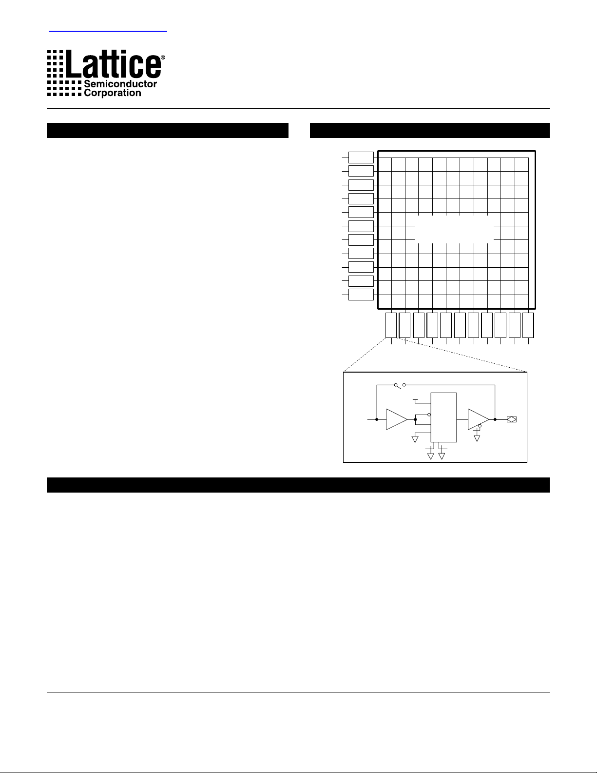
Functional Block Diagram (ispGDS22)
I/O Cell
A0
I/O Cell
A1
I/O Cell
A2
I/O Cell
A3
I/O Cell
A4
A5
Bank A
A6
A7
A8
A9
A10
I/O Cell
I/O Cell
I/O Cell
I/O Cell
I/O Cell
I/O Cell
I/O Cell
Switch
Matrix
PROGRAMMABLE
SWITCH MATRIX
I/O Cell
I/O Cell
I/O Cell
I/O Cell
B9B8B7
B10
Closed only when C0=1 and C1=0
4:1 MUX
Vcc
0 1
1 0
1 1
0 0
C2
I/O Cell
I/O Cell
I/O Cell
I/O Cell
I/O Cell
I/O Cell
B6B5B4B3B2B1B0
C1
Bank B
C0
TM
I/O Cell
Description
2
The Lattice Semiconductor ispGDS™ family is an ideal solution
for reconfiguring system signal routing or replacing DIP switches
used for feature selection. With today’s demands for customer
ease of use, there is a need for hardware which is easily
reconfigured electronically without dismantling the system. The
ispGDS devices address this challenge by replacing conventional
switches with a software configurable solution. Since each I/O pin
can be set to an independent logic level, the ispGDS devices can
replace most DIP switch functions with about half the pin count,
and without the need for additional pull-up resistors. In addition
to DIP switch replacement, the ispGDS devices are useful as
signal routing cross-matrix switches. This is the only non-volatile
device on the market which can provide this flexibility .
With a maximum tpd of 7.5ns, and a typical active Icc of only 25
mA, these devices provide maximum performance at very low
power levels. The ispGDS devices may be programmed in-system, using 5 volt only signals, through a simple 4-wire programming interface. The ispGDS devices are manufactured using
Copyright © 1997 Lattice Semiconductor Corp. All brand or product names are trademarks or registered trademarks of their respective holders. The specifications and information herein are subject
to change without notice.
Lattice Semiconductor’s advanced non-volatile E
which combines CMOS with Electrically Erasable (E
technology . High speed erase times (<100ms) allow the devices
to be reprogrammed quickly and efficiently .
Each I/O macrocell can be configured as an input, an inverting
or non-inverting output, or a fixed TTL high or low output. Any
I/O pin can be driven by any other I/O pin in the opposite bank.
A single input can drive one or more outputs in the opposite bank,
allowing a signal (such as a clock) to be distributed to multiple destinations on the board, under software control. The I/Os accept
and drive TTL voltage levels.
Unique test circuitry and reprogrammable cells allow complete
AC, DC, and functional testing during manufacture. As a result,
Lattice Semiconductor is able to deliver 100% field programmability and functionality of all Lattice Semiconductor
addition, 10,000 erase/write cycles and data retention in excess
of 20 years are specified.
LATTICE SEMICONDUCTOR CORP., 5555 Northeast Moore Ct., Hillsboro, Oregon 97124, U.S.A. July 1997
Tel. (503) 268-8000; 1-800-LATTICE; FAX (503) 268--8037; http://www.latticesemi.com
ispgds_02
CMOS process
2
) floating gate
products. In
Specifications ispGDS
ispGDS Ordering Information
Commercial Grade Specifications
Matrix Size I/O Pins Tpd (ns) Isb (mA) Icc (mA) Ordering # Package
11 x 11 22 7.5 25 40
9 x 9 18 7.5 25 40 ispGDS18-7P 24-Pin Plastic DIP
7 x 7 14 7.5 25 40
Part Number Description
ispGDS22-7P 28-Pin Plastic DIP
ispGDS22-7J 28-Lead PLCC
ispGDS14-7P 20-Pin Plastic DIP
ispGDS14-7J 20-Lead PLCC
ispGDS22
ispGDS18
ispGDS14
Device Name
Speed (ns)
XXXXXXXX XX X X
_
Package
Blank = CommercialGrade
P = Plastic DIP
J = PLCC
2
K
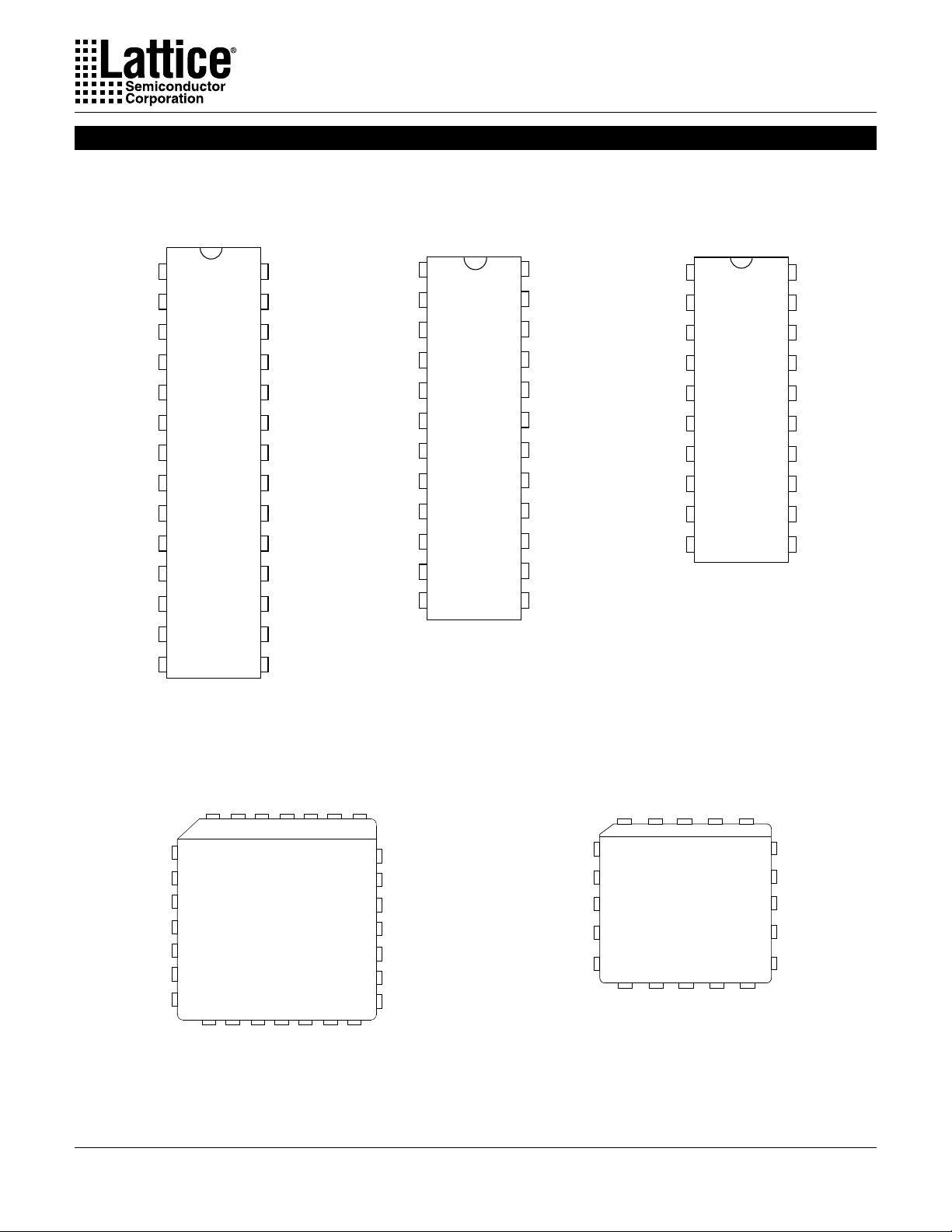
Pin Configuration
Specifications ispGDS
A0
A1
A2
SDI
A3
A4
Vcc
A5
A6
A7
MODE
A8
A9
A10
28-Pin DIP
128
B0
B1
B2
SDO
B3
ispGDS
21
B4
B5
GND
B6
B7
SCL
B8
B9
B10
22
7
14 15
A0
A1
A2
SDI
A3
Vcc
A4
A5
MODE
A6
A7
A8
24-Pin DIP 20-Pin DIP
1
ispGDS
18
6
12
24
18
13
B0
B1
B2
SDO
B3
B4
GND
B5
SCLK
B6
B7
B8
SDI
Vcc
MODE
A0
A1
A2
A3
A4
A5
A6
1
ispGDS
5
14
10
20
15
11
B0
B1
B2
SDO
B3
GND
SCLK
B4
B5
B6
A3
A4
Vcc
A5
A6
A7
MODE
28-Pin PLCC 20-Pin PLCC
SDIA2A1
5
7
ispGDS22
9
11
12 14 16 18
A8
A9
A0
B0
B1
B2
2
28426
25
SDO
B3
B4
23
B5
GND
21
B6
19
B7
B9
A10
B10
B8
SCLK
4
SDI
Vcc
ispGDS14
6
A3
MODE
8
A4
3
A0A1A2
2
10
B6A6A5 B5 B4
B0
B1
20
18
B2
SDO
16
B3
GND
SCLK
14
12

Specifications ispGDS
ispGDS Family Overview
There are three members of the ispGDS family, the ispGDS22,
ispGDS18, and ispGSD14. The numerical portion of the part
name indicates the number of I/O cells available. All of the
devices are available in a DIP package, with the ispGDS22 and
ispGDS14 also available in a PLCC package. Each of the
devices operate identically, with the only difference being the
number of I/O cells available.
The ispGDS devices are all programmed through a four-pin
interface, using TTL level signals. The four dedicated programming pins are named MODE, SDI, SDO, and SCLK. No highvoltage is needed, as the voltages needed for programming are
generated internally. Programming of the entire device, including erasure, can be done in less than one second. During the
programming operation, all I/O pins will be tri-stated. Further
details of the programming process can be found in the InSystem Programming section later in this datasheet.
The I/O cells in each device are divided equally into two banks
(Bank A and Bank B). Each I/O cell can be configured as an
input, an inverting output, a non-inverting output, or set to a fixed
TTL high or low. A switch matrix connects the I/O banks,
allowing an I/O cell in one bank to be connected to any of the I/
O cells in the other bank. A single I/O cell configured as an input
can drive one or more I/O cells in the other bank. The full I/O
macrocell, which is identical for each of the I/O pins, is shown
below. The allowable configurations are shown on the following
page.
Device Programming
The ispGDS family of devices uses a standard JEDEC file, as
used for programmable logic devices, to describe device programming information. Popular logic compilers, such as ABEL
and CUPL, can produce the JEDEC files for these devices.
The JEDEC files can be used to program the ispGDS devices in
a number of ways, which are shown in the section titled ISP
Architecture and Programming.
Electronic Signature
An electronic signature word is provided with every ispGDS
device. It contains 32 bits of reprogrammable memory that can
contain user defined data. Some uses include user ID codes,
revision numbers, or inventory control.
NOTE: The electronic signature is included in checksum
calculations. Changing the electronic signature will alter the
fuse checksum in the JEDEC fusemap.
In-System Programmability
The ispGDS family of devices feature In-System Programmable
technology. By integrating all the high voltage programming
circuitry on-chip, programming can be accomplished by simply
shifting data into the device. Once the function is programmed,
the non-volatile E2CMOS cells will not lose the pattern even
when the power is turned off.
All necessary programming is done via four TTL level logic
interface signals. These four signals are fed into the on-chip
programming circuitry where a state machine controls the
programming. The interface signals are Serial Data In (SDI),
Serial Data Out (SDO), Serial Clock (SCLK) and Mode (MODE)
control. For details on the operation of the internal state
machine and programming of ispGDS devices please refer to
the ISP Architecture and Programming section in this Data
Book.
4

I/O Macrocell
Specifications ispGDS
Closed only when C0=1 and C1=0
Switch
Matrix
I/O Macrocell Configurations
From
Switch
Matrix
From
Switch
Matrix
Vcc
C2
4:1 MUX
0 1
1 0
1 1
0 0
C1
Configuration for Active High Output
- C0 = 0.
- C1 = 1.
- C2 = 1.
Configuration for Active Low Output
- C0 = 0.
- C1 = 0.
- C2 = 1.
C0
Vcc
To
Switch
Matrix
Note 1: The development software configures all of the architecture control bits and checks for proper pin usage automatically.
Note 2: The default configuration for unused pins is for all configuration bits set to one, which produces a tri-stated output.
Configuration for Fixed TTL High Output
- C0 = 0.
- C1 = 1.
- C2 = 0.
Configuration for Fixed TTL Low Output
- C0 = 0.
- C1 = 0.
- C2 = 0.
Configuration for Dedicated Input
- C0 = 1.
- C1 = 0.
- C2 = 1.
5

Specifications ispGDS
Absolute Maximum Ratings
Supply voltage VCC........................................ –.5 to +7V
Input voltage applied .......................... –2.5 to VCC +1.0V
Off-state output voltage applied ......... –2.5 to VCC +1.0V
Storage Temperature ................................–65 to 150°C
Ambient Temperature with
Power Applied ...........................................–55 to 125°C
1.Stresses above those listed under the “Absolute Maximum
Ratings” may cause permanent damage to the device. These
are stress only ratings and functional operation of the device
at these or at any other conditions above those indicated in
the operational sections of this specification is not implied
(while programming, follow the programming specifications).
(1)
Recommended Operating Cond.
Commercial Devices:
Ambient T emperature (TA) ...............................0 to 75°C
Supply voltage (VCC)
with Respect to Ground ..................... +4.75 to +5.25V
DC Electrical Characteristics
Over Recommended Operating Conditions (Unless Otherwise Specified)
SYMBOL PARAMETER CONDITION MIN. TYP.2MAX. UNITS
VIL Input Low Voltage Vss – 0.5 — 0.8 V
VIH Input High Voltage 2.0 — Vcc+1 V
IIL Input or I/O Low Leakage Current 0V ≤ VIN ≤ VIL (MAX.) ——–10 µA
IIH Input or I/O High Leakage Current 3.5V ≤ VIN ≤ VCC ——10 µA
VOL Output Low Voltage IOL = MAX. Vin = VIL or VIH ——0.5 V
VOH Output High Voltage IOH = MAX. Vin = VIL or VIH 2.4 —— V
IOL Low Level Output Current —— 8mA
IOH High Level Output Current ——–3.2 mA
1
IOS
Output Short Circuit Current VCC = 5V VOUT = 0.5V TA = 25°C –30 —–130 mA
COMMERCIAL
ISB Standby Power Inputs = 0V Outputs open L-7 — 15 25 mA
Supply Current
ICC Operating Power VIL = 0.5V VIH = 3.0V L -7 — 25 40 mA
Supply Current f
1) One output at a time for a maximum duration of one second. Vout = 0.5V was selected to avoid test problems caused by tester
ground degradation. Characterized but not 100% tested.
2) T ypical values are at Vcc = 5V and TA = 25 °C
toggle = 15MHz Outputs Open
Capacitance (TA = 25°C, f = 1.0 MHz)
SYMBOL PARAMETER MAXIMUM* UNITS TEST CONDITIONS
C
I/O
*Characterized but not 100% tested.
I/O Capacitance (as input or output) 8 pF VCC = 5.0V , VI = 2.0V
6

AC Switching Characteristics
Specifications ispGDS
Over Recommended Operating Conditions
COM
PARAMETER UNITS
TEST
COND.
DESCRIPTION
MIN. MAX.
tpd A Input to Output Delay One Input Driving One Output 1 7.5 ns
fmax A Maximum Input Frequency One Output Switching — 50 MHz
twh A Input Pulse Duration, High 10 — ns
twl A Input Pulse Duration, Low 10 — ns
Switching Waveforms
INP U T
OUTPUT
Input to Output Delay
VALID IN P U T
t
pd
INP U T
t
wh
1/ fmax
t
wl
Input Pulse Width/ Fmax
Switching Test Conditions
Input Pulse Levels GND to 3.0V
Input Rise and Fall Times 2ns 10% – 90%
Input Timing Reference Levels 1.5V
Output Timing Reference Levels 1.5V
Output Load See Figure
3-state levels are measured 0.5V from steady-state
active level.
FROM OUTPUT (O/Q)
UNDER TEST
+5V
R
1
TEST POINT
Output Load Conditions (see figure)
T est Condition R
1 R2 CL
A 470Ω 390Ω 50pF
C *
R
2
*C
INCLUDES TEST FIXTURE AND PROBE CAPACITANCE
L
L
7

Typical AC and DC Characteristic Diagrams
Specifications ispGDS
Normalized Tpd vs Vcc
1.3
1.2
1.1
1
0.9
Normalized Tpd
0.8
4.50 4.75 5.00 5.25 5.50
Supply Voltage (V)
Normalized Tpd vs Temp
1.3
1.2
1.1
1
0.9
Normalized Tpd
0.8
0.7
-55 -25 0 25 5 0 75 1 00 125
PT H->L
PT L->H
Temperature (deg. C)
PT H->L
PT L->H
Delta Tpd vs # of Outputs
Switching
2.25
2
1.75
1.5
1.25
1
0.75
0.5
Delta Tpd (ns)
0.25
0
1234567891011
RISE
FALL
Number of Outputs Switching
Delta Tpd vs Output Loading
14
12
10
8
6
4
2
0
Delta Tpd (ns)
-2
-4
0 50 100 150 200 250 300
RISE
FALL
Output Loading (pF)
Input Clamp (Vik)
0
10
20
30
40
50
Iik (mA)
60
70
80
90
-2.00 -1.50 -1.00 -0.50 0.00
Vik (V)
Delta Icc vs Vin (1 input)
7
6
5
4
3
2
Delta Icc (mA)
1
0
0.00 0.50 1.00 1.50 2.00 2.50 3.00 3.50 4.00
Vin (V)
Vol vs Iol
3
2.5
2
1.5
Vol (V)
1
0.5
0
0.00 20.00 40.00 60.00 80.00
Iol (mA)
Normalized Icc vs Vcc
1.20
1.10
1.00
0.90
Normalized Icc
0.80
4.50 4.75 5.00 5.25 5.50
Supply Voltage (V)
Voh vs Ioh
5
4
3
2
Voh (V)
1
0
0.00 10.00 20.00 30.00 40.00 50.00 60.00
Ioh(mA)
Normalized Icc vs Temp
1.2
1.1
1
0.9
Normalized Icc
0.8
-55 -25 0 25 50 75 100 125
Temperature (deg. C)
Voh vs Ioh
4.25
4
3.75
3.5
Voh (V)
3.25
3
0.00 1.00 2.00 3.00 4.00
Ioh(mA)
Normalized Icc vs Freq.
1.30
1.20
1.10
1.00
Normalized Icc
0.90
0 25 50 7 5 100
Frequency (MHz)
8
 Loading...