

Page 1

User Guide
FPGA-UG-02057 Version 1.0
June 2018
iCE40 UltraPlus 6:1 MIC Aggregation over SPI
Demo
Page 2

iCE40 UltraPlus 6:1 MIC Aggregation over SPI Demo
User Guide
Contents
Acronymns in This Document ........................................................................................................................................ 3
1. Introduction .......................................................................................................................................................... 4
2. Functional Description ........................................................................................................................................... 4
2.1. Demo Design Overview ................................................................................................................................ 4
3. Demo Setup .......................................................................................................................................................... 5
3.1. Hardware Requirements ............................................................................................................................... 5
3.2. Software Requirements ................................................................................................................................ 5
3.3. Configuring the MDP Board .......................................................................................................................... 5
3.3.1. Setting Jumpers and Switches ................................................................................................................... 5
4. Programming the Demo ........................................................................................................................................ 7
4.1. Programming the Bitstream to the iCE40 UltraPlus MDP ............................................................................... 7
5. Running the Demo ................................................................................................................................................. 9
5.1. Using Windows Application .......................................................................................................................... 9
5.2. Oscilloscope Connection Points .................................................................................................................. 10
Appendix A. Schematic Diagram .................................................................................................................................. 11
Appendix B. Bill of Materials ........................................................................................................................................ 12
Technical Support ....................................................................................................................................................... 13
Revision History .......................................................................................................................................................... 13
Figures
Figure 2.1. iCE40 UltraPlus 6:1 MIC Aggregation over SPI Demo Overview ..................................................................... 4
Figure 2.2. iCE40 UltraPlus 6:1 MIC Aggregation over SPI Demo Block Diagram .............................................................. 4
Figure 3.1. iCE40 UltraPlus MDP Configuration .............................................................................................................. 5
Figure 3.2. 8 to 1 Mic Aggregator Board (Daughter Board) ............................................................................................. 6
Figure 3.3. iCE40 UltraPlus MDP and 8 to 1 Mic Aggregator Board ................................................................................. 6
Figure 4.1. Device Properties ......................................................................................................................................... 7
Figure 5.1. J30 Section on MDP Board ......................................................................................................................... 10
Figure 5.2. Header to Connect to the Oscilloscope ....................................................................................................... 10
Tables
Table 3.1. Detailed Information of the Board Configuration ........................................................................................... 6
All other brand or product names are trademarks or registered trademarks of their respective holders. The specifications and information herein are subject to change without notice.
2 FPGA-UG-02057-1.0
© 2018 Lattice Semiconductor Corp. All Lattice trademarks, registered trademarks, patents, and disclaimers are as listed at www.latticesemi.com/legal.
Page 3
iCE40 UltraPlus 6:1 MIC Aggregation over SPI Demo
Acronym
Definition
I²S
Inter-IC Sound
PCM
Pulse Code Modulation
PDM
Pulse Density Modulation
FPGA
Field-Programmable Gate Array
MDP
Mobile Development Platform
SPI
Serial Peripheral Interface
SSP
System Solution Platform
User Guide
Acronymns in This Document
A list of acronyms used in this document.
All other brand or product names are trademarks or registered trademarks of their respective holders. The specifications and information herein are subject to change without notice.
FPGA-UG-02057-1.0 3
© 2018 Lattice Semiconductor Corp. All Lattice trademarks, registered trademarks, patents, and disclaimers are as listed at www.latticesemi.com/legal.
Page 4
iCE40 UltraPlus 6:1 MIC Aggregation over SPI Demo
iCE40
UltraPlus
Device
6 PDM
microph ones
Applications
SPI
PDM2PCM
CIC Filter 1
CIC Filter 2
CIC Filter 3
CIC Filter 4
CIC Filter 5
CIC Filter 6
Compensation Filter 1
Compensation Filter 2
Compensation Filter 3
Compensation Filter 4
Compensation Filter 5
Compensation Filter 6
PDM data from
daughter board’s
6 microphones
iCE40 UltraPlus
Audio
Buffer
SPI Bus
Applications
(SPI master)
Control
Signals
PCM
Data
SPI
Signals
User Guide
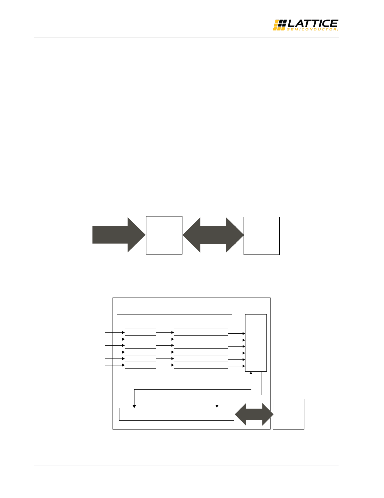
1. Introduction
I²S (Inter-IC Sound) bus is widely used to communicate Pulse Code Modulation (PCM) audio data between integrated
circuits in an electronic device. The standard I²S protocol, however, is designed to transfer only two channels (LEFT and
RIGHT) on a data line. This limitation can be addressed by using Serial Peripheral Interface (SPI), an interface bus
commonly used to send data between microcontrollers and small peripherals.
The iCE40 UltraPlus™ 6:1 MIC Aggregation over SPI demo addresses a market opportunity to transfer up to six
microphones channels using an SPI bus.
2. Functional Description
2.1. Demo Design Overview
The iCE40 UltraPlus 6:1 MIC Aggregation over SPI demo implements an SPI bus using the iCE40 UltraPlus FPGA. The
demo uses FPGA-B on the primary iCE40 UltraPlus Mobile Development Platform (MDP), plus a daughter board with six
Pulse Density Modulation (PDM) microphones for the input sources. Sound generated by the microphones can be
captured and heard through Windows applications. This version of the the project design uses the Lattice Radiant
Software tool.
Figure 2.1 shows an overview diagram of the iCE40 UltraPlus 6:1 MIC Aggregation over SPI demo.
Figure 2.2 shows the iCE40 UltraPlus 6:1 MIC Aggregation over SPI demo block diagram.
Figure 2.1. iCE40 UltraPlus 6:1 MIC Aggregation over SPI Demo Overview
Figure 2.2. iCE40 UltraPlus 6:1 MIC Aggregation over SPI Demo Block Diagram
All other brand or product names are trademarks or registered trademarks of their respective holders. The specifications and information herein are subject to change without notice.
© 2018 Lattice Semiconductor Corp. All Lattice trademarks, registered trademarks, patents, and disclaimers are as listed at www.latticesemi.com/legal.
4 FPGA-UG-02057-1.0
Page 5

iCE40 UltraPlus 6:1 MIC Aggregation over SPI Demo
J23 Pins 2-3
SW5-1 ON
SW5-2 OFF
J28 – Disconnect
J27 Pins 9-10
J26 Pins 9-10
R30
J25 Pins 1-2
J25 Pins 5-6
J19 Pins 1-2 and
Pins 3-4 (Horizontal)
J17 Pins 9-10
User Guide
3. Demo Setup
The following hardware and software are required to run the iCE40 UltraPlus 6:1 MIC Aggregation over SPI demo.
3.1. Hardware Requirements
iCE40 UltraPlus MDP (PN: iCE40UP5K-MDP-EVN)
8 to 1 Mic Aggregator Board (Daughter Board) (PN: LF-81AGG-EVN)
3.2. Software Requirements
Lattice Radiant 1.0
Radiant Programmer (Version 1.0 or later)
System Solution Platform (SSP)
Note: SSP installer and installation guide are included with this solution under SSP folder. Follow the instructions in the
guide to install this application properly.
3.3. Configuring the MDP Board
3.3.1. Setting Jumpers and Switches
Board reconfiguration is needed before running this demo. Figure 3 highlights (in orange boxes) all switches and
jumpers need to be verified or reconfigured on Mobile Development Platform (MDP) board.
Figure 3.1. iCE40 UltraPlus MDP Configuration
Note: This demo uses FPGA-B.
All other brand or product names are trademarks or registered trademarks of their respective holders. The specifications and information herein are subject to change without notice.
FPGA-UG-02057-1.0 5
© 2018 Lattice Semiconductor Corp. All Lattice trademarks, registered trademarks, patents, and disclaimers are as listed at www.latticesemi.com/legal.
Page 6

iCE40 UltraPlus 6:1 MIC Aggregation over SPI Demo
Items
Configuration
Description
J17, J26, J27
Shunt pin 9-10
Disable ICE40UP5K_A/C/D devices.
J25
Shunt pin 1-2, 5-6
Enable ICE40UP5K_B device.
J28
Disconnect all
Disable Board control for programming SPI Flash.
J19
Shunt pin 1-2, 3-4 (horizontal)
Enable iCE40 CRAM Programming
J23
Shunt pin 2-3
Use Xtal U14 as clock source.
SW2
Set to ON
Power switch, slide down for power-on.
SW5
Set SW5-1 to ON, and SW5-2 to off.
Select ICE40UP5K_B as target device.
User Guide
Table 3.1 lists the detailed information of these configurations on switches and jumpers.
Table 3.1. Detailed Information of the Board Configuration
Before programming the MDP, perform the following steps:
1. On the iCE40 Ultraplus MDP, install a 0-Ω (0603) resistor at R30 if not yet installed.
2. Connect the 8 to 1 Mic Aggregator Board on top of the MDP board.
Figure 3.2. 8 to 1 Mic Aggregator Board (Daughter Board)
Figure 3.3. iCE40 UltraPlus MDP and 8 to 1 Mic Aggregator Board
All other brand or product names are trademarks or registered trademarks of their respective holders. The specifications and information herein are subject to change without notice.
6 FPGA-UG-02057-1.0
© 2018 Lattice Semiconductor Corp. All Lattice trademarks, registered trademarks, patents, and disclaimers are as listed at www.latticesemi.com/legal.
Page 7

iCE40 UltraPlus 6:1 MIC Aggregation over SPI Demo
User Guide
4. Programming the Demo
4.1. Programming the Bitstream to the iCE40 UltraPlus MDP
Use Radiant Programmer to program the bitstream to the iCE40 UltraPlus MDP:
1. Connect the iCE40 UltraPlus MDP to the PC using a USB cable.
2. Power ON the iCE40 UltraPlus MDP.
3. Start the Radiant Programmer software tool (version 1.0 or later).
4. In the Getting Started dialog box, select Create a new project file from a scan and click OK.
5. The iCE40 UltraPlus device is detected and displayed in the main interface.
Device Family: iCE40 UltraPlus
Device: iCE40UP5K
Right-click on the device and select Device Properties in the context menu.
6. In the Device Properties dialog box, apply the settings as shown in Figure 4.1.
Figure 4.1. Device Properties
All other brand or product names are trademarks or registered trademarks of their respective holders. The specifications and information herein are subject to change without notice.
FPGA-UG-02057-1.0 7
© 2018 Lattice Semiconductor Corp. All Lattice trademarks, registered trademarks, patents, and disclaimers are as listed at www.latticesemi.com/legal.
Page 8

iCE40 UltraPlus 6:1 MIC Aggregation over SPI Demo
User Guide
Target Memory: Set to Compressed Random Access Memory (CRAM).
Port Interface: Set to Slave SPI.
Access Mode: Set to Direct Programming.
Operation: Set to Fast Configuration.
Programming File: Path of the bitstream file for demo.
3. Click OK to exit the Device Properties dialog box.
Click the Program Device button on the main interface to download the bitstream file.
All other brand or product names are trademarks or registered trademarks of their respective holders. The specifications and information herein are subject to change without notice.
8 FPGA-UG-02057-1.0
© 2018 Lattice Semiconductor Corp. All Lattice trademarks, registered trademarks, patents, and disclaimers are as listed at www.latticesemi.com/legal.
Page 9

iCE40 UltraPlus 6:1 MIC Aggregation over SPI Demo
User Guide
5. Running the Demo
5.1. Using Windows Application
To run the demo:
1. Load the bitstream into the FPGA-B on the iCE40 UltraPlus MDP.
2. Using Windows Explorer, navigate to the …/SSP folder.
3. Delete the previously run data.txt file.
4. Run the batch file named run_pcm_emu.bat to start capturing audio data on the microphone sensor. A new file
data.txt file is created.
5. Press Ctrl + C to stop the audio capture.
6. Copy the generated data.txt file to the ../tool folder.
7. In the ..tool/ folder, run the pcm_processor.exe file.
This converts the data.txt file into hexadecimal and decimal files for checking. In addition, a wave file is also generated
for audio playback.
Figure 5.1. Running pcm_processor.exe
.
Figure 5.2. Files Generated by Running pcm_processor.exe
All other brand or product names are trademarks or registered trademarks of their respective holders. The specifications and information herein are subject to change without notice.
FPGA-UG-02057-1.0 9
© 2018 Lattice Semiconductor Corp. All Lattice trademarks, registered trademarks, patents, and disclaimers are as listed at www.latticesemi.com/legal.
Page 10

iCE40 UltraPlus 6:1 MIC Aggregation over SPI Demo
User Guide
5.2. Oscilloscope Connection Points
You can use an oscilloscope to observe signals of the SPI interface. The signals are available at FPGA-B header J30 on
the iCE40 UltraPlus MDP.
Figure 5.1. J30 Section on MDP Board
Figure 5.2. Header to Connect to the Oscilloscope
All other brand or product names are trademarks or registered trademarks of their respective holders. The specifications and information herein are subject to change without notice.
10 FPGA-UG-02057-1.0
© 2018 Lattice Semiconductor Corp. All Lattice trademarks, registered trademarks, patents, and disclaimers are as listed at www.latticesemi.com/legal.
Page 11

iCE40 UltraPlus 6:1 MIC Aggregation over SPI Demo
User Guide
Appendix A. Schematic Diagram
5
VDD
C1
C5
10uF
0.1uF
C0603
6.3V
C2
10uF
C0603
6.3V
C0402
16V
VDD
C6
0.1uF
C0402
16V
VDD
R8 10K
C13
0.1uF
C0402
16V
R13 10K
C4
0.1uF
C0402
16V
5
D D
C C
VDD
B B
A A
MIC1
3
VDD
2
LR
R0402
5
GND
MIC2
3
VDD
R10
10K
R0402
2
LR
5
GND
PART_NUMBER = MP34DB02TR
Manufacturer = STMicroelectronics
MIC3
3
VDD
2
LR
R0402
5
GND
MIC4
3
VDD
R15
10K
R0402
2
LR
5
GND
PART_NUMBER = MP34DB02TR
Manufacturer = STMicroelectronics
MP34DB02TR
MP34DB02TR
MP34DB02TR
MP34DB02TR
1
R7 33
CLK
4
R9 33
DOUT
MIC12
4
R11 33
DOUT
1
R6 33
CLK
1
R12 33
CLK
4
R17 33
DOUT
MIC34
4
R16 33
DOUT
1
R14 33
CLK
CLK
Route CLK Daisy - Chain
R0402
R0402
R0402
R0402
R0402
R0402
R0402
R0402
4
VDD
R26
10K
R0402
R23
10K
R0402
R0402
R0402
3
2
5
3
2
5
3
2
5
3
2
5
C8
C12
10uF
0.1uF
C0603
C0402
6.3V
16V
R19 10K
VDD
C9
0.1uF
C0402
16V
VDD
C11
C7
0.1uF
10uF
C0402
C0603
16V
6.3V
4
VDD
R28 10K
C10
0.1uF
C0402
16V
3
MIC5
VDD
MP34DB02TR
LR
GND
MIC6
VDD
MP34DB02TR
LR
GND
PART_NUMBER = MP34DB02TR
Manufacturer = STMicroelectronics
MIC7
VDD
MP34DB02TR
LR
GND
MIC8
VDD
MP34DB02TR
LR
GND
PART_NUMBER = MP34DB02TR
Manufacturer = STMicroelectronics
1
CLK
4
DOUT
4
DOUT
1
CLK
1
CLK
4
DOUT
4
DOUT
1
CLK
3
R18 33
R20 33
MIC56
R27 33
R25 33
R21 33
R29 33
MIC78
R24 33
R22 33
R0402
R0402
R0402
R0402
R0402
R0402
R0402
R0402
VDD
R33
120
R0402
DNL
R34
60
R0402
DNL
C15
0.1uF
C0402
16V
DNL
2
1
8 to 1 Mic Aggregator Card
VDD
C14
10uF
C0603
6.3V
WS
R0402
MODE LED YELLOW
MODE_SWITCH
PART_NUMBER = TL1015AF160QG
Manufacturer = E-Switch
1
3
CLK
R0402
Each microphone requires air hole
Place L\R microphone pairs next to each other
Place 0 ohm resistors close to header
Route CLK Daisy-Chain
Resistors and 100nF Capacitors are 0402 size
10uF Capacitors are 6.3V minimum 0603 size
LEDs are 0603 size
5
7
9
PART_NUMBER = NPTC052KFMS-RC
Manufacturer = Sullins Connector Solutions
1
MIC12
R4 0
MIC34
R3 0
MIC56
R1 0
MIC78
R2 0
Layout Note : Place
R33,R34 & C15 close
to R22
2
R30
470
R0402
D1
POWER LED GREEN
PART_NUMBER = 150060VS75000
Manufacturer = Wurth Electronics Inc
Notes:
WS Low = LED On
WS Hi-Z = LED Off and read SWITCH
SWITCH pushed = LED On and WS Low
J15
NPTC052KFMS-RC
1
R0402
3
R0402
5
R0402
7
R0402
9
PART_NUMBER = NPTC052KFMS-RC
Manufacturer = Sullins Connector Solutions
Title
Title
Title
Size Document Number Rev
Size Document Number Rev
Size Document Number Rev
B
B
B
Date: Sheet
Date: Sheet of
Date: Sheet of
R31
470
R0402
R32 10K
D2
Manufacturer = Wurth Electronics Inc.
PART_NUMBER = 150060YS75000
VDD
2
1
2
4
R5 0
3
4
6
WS
5
6
NC_AMP
8
7
8
10
9
10
8 to 1 Mic Aggregator Card
8 to 1 Mic Aggregator Card
8 to 1 Mic Aggregator Card
305-PD-17-0490 A.0
305-PD-17-0490 A.0
305-PD-17-0490 A.0
SW1
J13
NPTC052KFMS-RC
2
1
2
4
3
4
6
5
6
8
7
8
10
9
10
of
2 2Thursday, July 20, 2017
2 2Thursday, July 20, 2017
2 2Thursday, July 20, 2017
8 to 1 Mic Aggregator Card
All other brand or product names are trademarks or registered trademarks of their respective holders. The specifications and information herein are subject to change without notice.
© 2018 Lattice Semiconductor Corp. All Lattice trademarks, registered trademarks, patents, and disclaimers are as listed at www.latticesemi.com/legal.
FPGA-UG-02057-1.0 11
Page 12

iCE40 UltraPlus 6:1 MIC Aggregation over SPI Demo
Item
Reference
Designator
QTY
Description
Package
Manufacturer
Part
Number
Notes
1
C1,C2,C7,C8,
C14
5
Capacitor Ceramic 10 uF
20% 6.3V X5R 0603
0603
Murata
Electronics
GRM188R61A475ME15D
2
C4,C5,C6,C9,
C10,C11,C12,
C13
8
Capacitor Ceramic 0.1 uF
10% 16V X7R 0402
0402
Murata
Electronics
GRM155R71C104KA88J
3
C15
1
Capacitor Ceramic 0.1 uF
10% 16V X7R 0402
0402
Murata
Electronics
GRM155R71C104KA88J
DNL
4
D1 1 LED Green 0603
0603
Wurth
150060VS75000
5
D2 1 LED Yellow 0603
0603
Wurth
150060YS75000
6
J13,J15
2
Connector Header
Female 2x5 0.1" Pitch
2x5 0.1"
Pitch
Sullins
NPTC052KFMS-RC
7
MIC1,MIC2,
MIC3,MIC4,
MIC5,MIC6,
MIC7,MIC8
8
Microphone PDM
Omnidirectional -26DB
RHLGA
(3x4x1) mm
4LD
STMicroelectronics
MP34DB02TR
8
R1,R2,R3,R4,
R5
5
Resistor 0.0 Ω 5% 1/16W
0402
0402
Yageo
RC0402JR-070RL
9
R6,R7,R9,R11,
R12,R14,R16,
R17,R18,R20,
R21,R22,R24,
R25,R27,R29
16
Resistor 33 Ω 5% 1/16W
0402
0402
Yageo
RC0402JR-0733RL
10
R8,R10,R13,
R15,R19,R23,
R26,R28,R32
9
Resistor 10 K Ω 5%
1/16W 0402
0402
Yageo
RC0402JR-0710KL
11
R30,R31
2
Resistor 470 Ω 5%
1/16W 0402
0402
Yageo
RC0402FR-07470RL
12
R33
1
Resistor 120 Ω 1%
1/16W 0402
0402
Yageo
RC0402FR-07120RL
DNL
13
R34
1
Resistor 62 Ω 5% 1/16W
0402
0402
Yageo
RC0402FR-0762RL
DNL
14
SW1
1
Switch Push Button
Momentary SPST-NO
0.05A 12 V
3.90 mm x
2.90 mm
E-Switch
TL1015AF160QG
15
8 to 1 MIC
AGGREGATOR
CARD REVA.0
PCB
1
Bare PCB
Pactron
305-PD-17-0490
User Guide
Appendix B. Bill of Materials
8 to 1 Mic Aggregator Board Bill of Materials
All other brand or product names are trademarks or registered trademarks of their respective holders. The specifications and information herein are subject to change without notice.
12 FPGA-UG-02057-1.0
© 2018 Lattice Semiconductor Corp. All Lattice trademarks, registered trademarks, patents, and disclaimers are as listed at www.latticesemi.com/legal.
Page 13

iCE40 UltraPlus 6:1 MIC Aggregation over SPI Demo
Date
Version
Change Summary
June 2018
1.0
Initial release.
Technical Support
For assistance, submit a technical support case at www.latticesemi.com/techsupport.
Revision History
User Guide
All other brand or product names are trademarks or registered trademarks of their respective holders. The specifications and information herein are subject to change without notice.
FPGA-UG-02057-1.0 13
© 2018 Lattice Semiconductor Corp. All Lattice trademarks, registered trademarks, patents, and disclaimers are as listed at www.latticesemi.com/legal.
Page 14

7th Floor, 111 SW 5th Avenue
Portland, OR 97204, USA
T 503.268.8000
www.latticesemi.com
 Loading...