

Page 1

iCE40 Ultra™ Mobile Development Platform User Guide
EB90 Version 1.1, June 2015
Page 2

iCE40 Ultra Mobile Development Platform User Guide
Introduction
This platform is designed to develop and demonstrate various mobile applications using the iCE40 Ultra device.
The board is in the form factor of a bar phone featuring various sensors and connectivity to external mobile software development platforms.
Kit Contents
The following items are included in the development kit:
• Main Board – The main board is mounted in lower plastic enclosures.
• Key Set – The key set includes keys A, B, C, and Custom. Key A is installed on the main unit by default.
• DragonBoard Interface Module
• Interconnecting Cables – The cables include USB mini-B cable, DragonBoard interface ribbon cable, and +5 V
supply flywire.
Variants
The unit is built in two variants with different sets of RGB LED and IR LED parts.
Variant A includes the following parts on the board:
• RGB LED used at D12: AEBMT-RGBZ by Advanced Optoelectronics Technology
• IR LED used at D7: SFH 4645 by Osram Opto Semiconductors
Variant B includes the following parts on the board:
• RGB LED used at D13: APTF1616SEEZGQBDC by Kingbright
• IR LED used at D7: VSMB2948SL by Vishay Semiconductor
The variants can be distinguished through the populated status of D12 and D13.
• Variant A: D12 is populated and D13 is not populated
• Variant B: D12 is not populated and D13 is populated
2
Page 3

iCE40 Ultra Mobile Development Platform User Guide
MAX44008 (I2C)
RGB ALS
APP PROCESSOR (SPI)
(10 pin CONN)
3.3v
BMP180 (I2C)
Pressure
IR LED (TX)
HIGH POWER
WHITE LED
JUMPER SEL
POOL-B I2C
POOL-A I2C
POWER SUPPLIES
(from USB / Battery)
FT2232H
SPI CONFIG FLASH (SPI)
USB
CHEETAH CONN
LSM330DLC (I2C)
Accel. & Gyro
HALL SENSOR
THESE CONNECTIONS VIA INTERCONNECT
[40 pin FPC connector]
TMD27711 (I2C)
Proximity & ALS #2
Key-socket selection
FINGERPRINT SENSOR I2S MIC#2
SPI
Li-ion BatteryCHARGER
Key-socket selection
RGB LED
I2S MIC#1 SMA CONN
CURRENT MEASURE
CURRENT
MEASURE
BLE Module
IR RX
LSM303DLHC (I2C)
Magentometer
SHT20 (I2C)
Humidity &Temp.
TMD27711 (I2C)
Proximity & ALS #1
POOL-B I2C
POOL-B I2C
3.3V
3.3V
SMA CONN
Operated together
Optional
CONFIG SPI & BANK 1
BANK 2
BANK 0
iCE5LP4KSWG36
SPI
UART
Demo Board Architecture
Figure 1 shows the demo board architecture. The different I2C sensors are split up and wired on two separate I2C
buses as Pool A and Pool B. The other sensors that are not I2C are either wired separately or are connected
instead of Pool B and other resources on the board. Changes to connectivity are user controllable and achieved by
means of changing the keys – a method to replace using multiple jumpers to re-route wiring to different resources.
Figure 1. Block Diagram
3
Page 4
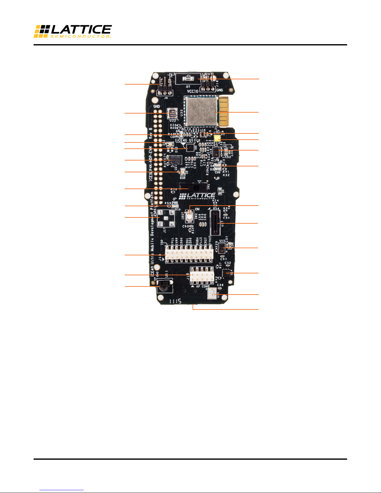
Figure 2. Top View of Main Unit
iCE40 Ultra Mobile Development Platform User Guide
Jumper selection between
IR and White High Power LEDs
BMP180
Pressure Sensor
CDONE LED
RGB LED
iCE40 Ultra
27 MHz
Oscillator
Barcode LED
(Red)
Power Switch
Power LED
SMA Footprint
J15 (Jumper
Pool Header)
IR LED (Emitter)
BLE Module
MAX4408 RGB ALS Sensor
High Power White LED
TMD2711 Proximity Sensor
External Power and
Charging Status Indicator
CRST Button
FPC1080A Fingerprint Sensor
TMD2711 Proximity Sensor
AP Connector
IR Rx (TSMP58000)
SHT20 Humidity Sensor
ADMP441 I2S Mic
USB Port
4
Page 5
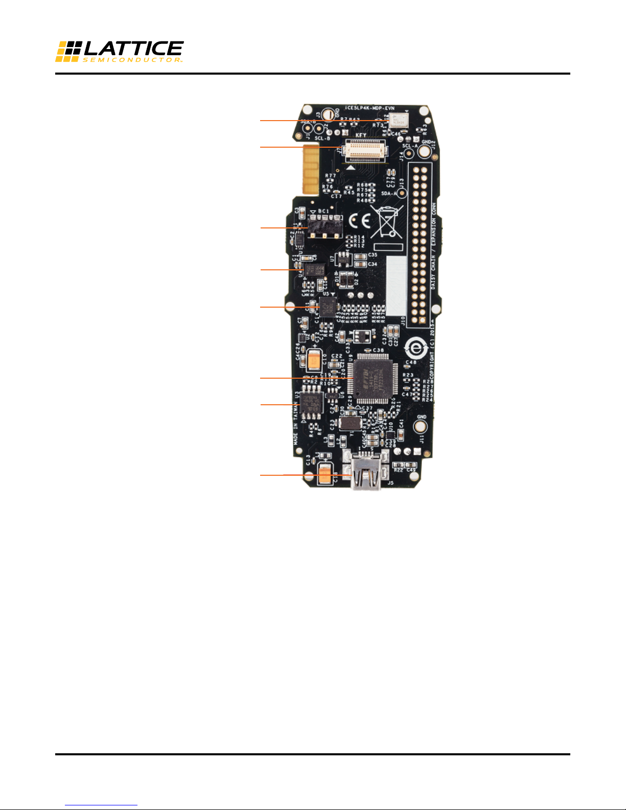
Figure 3. Bottom View of Main Unit
ADMP441 I2S Mic
LSM303DLHC
Magnetometer Sensor
LSM330DLC
Accelerometer and
Gyroscope Sensor
iCE40 Ultra Mobile Development Platform User Guide
Key Socket
Battery
Connector
FTDI FT2232H
M25P80
SPI Flash
USB Port
5
Page 6

iCE40 Ultra Mobile Development Platform User Guide
Features
• Supports BLE (Bluetooth Low Energy) module
• Supports OTA (Over-The-Air) configuration of FPGA
• Form factor similar to mobile phone
Sensor list
The following table lists the different sensors used on the board.
Table 1. Sensor List
Number Sensor Function Interface Sensor Part Number Manufacturer
1 RGB LED (Variant 1) Direct AEBMT-RGBZ AOT
2 RGB LED (Variant 2) Direct APTF1616SEEZGQBDC Kingbright
3 High Current IR Tx LED
(Variant A)
4 High Current IR Tx LED
(Variant B)
5 High Current Visible LED Direct XBDA WT-00-0000-
6 IR Rx Direct TSMP58000 Vishay Semiconductor
7 Proximity Sensor
(Two numbers)
8 RGB Light Sensor I2C MAX44008 Maxim-IC
9 Temperature Sensor I2C BMP180 (integrated) Bosch
10 Barometric Pressure I2C BMP180 Bosch
11 Accelerometer I2C LSM330DLC
12 Gyroscope I2C
13 Magnetometer I2C LSM303DLHC ST Micro
14 Humidity I2C SHT20 Sensirion
15 Hall Direct BU52051NV X-TR Rohm Semiconductor
16 Fingerprint SPI FPC1080A Fingerprints
17 MEMS Mic (Two numbers) I2S ADMP441 Invensense
Direct SFH4645 Osram Opto
Direct VSMB2948SL Vishay Semiconductor
Cree Inc.
00000LCE3
I2C TMD27711 A MS-TA OS USA Inc
ST Micro
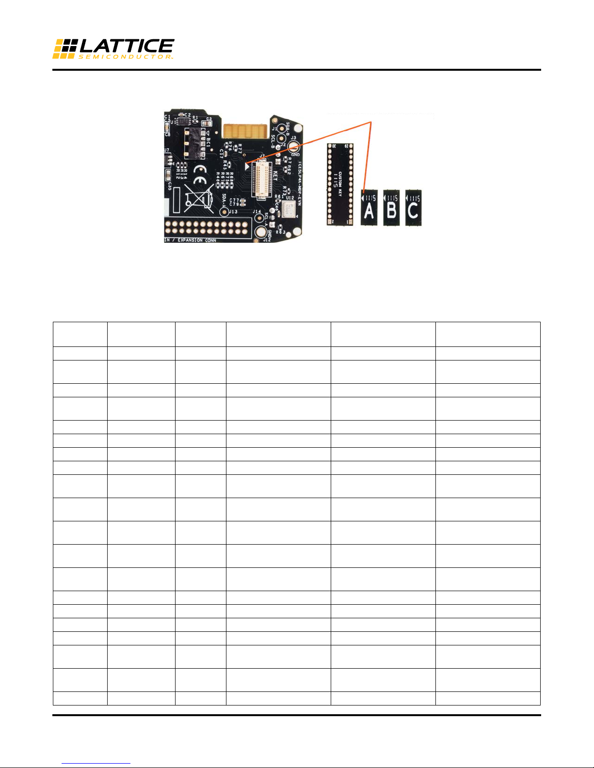
Key-socket Arrangement
Three predefined keys and one user defined key is provided to allow the user to change the wiring of the board
between different sensor sets as described in Table 2. The table also denotes pin assignments to the iCE40 Ultra
FPGA on the board. While selecting and inserting a particular key of choice, ensure that you align the aligning
arrow on the key and on the main PCB. The keys are mechanically delicate, and hence, you must be careful while
inserting and removing the keys. Figure 4 shows the four keys and socket on the main board.
6
Page 7
iCE40 Ultra Mobile Development Platform User Guide
Orient the direction of the key
using these arrows
Figure 4. Key-socket Arrangement
Pin assignments iCE40 Ultra FPGA
Table 2 lists the complete pin assignments for the iCE40 Ultra FPGA for the different keys and other hard wired
peripherals on the board
Table 2. Pin Assignment
Pin
Number Pin Name Bank
A4 VCCIO_0 Bank 0 3V3 3V3 3V3
B5 IOT_46B_G0 Bank 0 Not used / Optional ext
A6 RGB2 Bank 0 BLED (RGB LED) BLED (RGB LED) I2S_CE1 (Microphone 1)
B6 RGB1 Bank 0 GLED (RGB LED) GLED (RGB LED) I2S_SCK1 (Microphone
C6 RGB0 Bank 0 RLED (RGB LED) RLED (RGB LED) I2S_SD1 (Microphone 1)
A2 IRLED Bank 0 HPLED (IRLED or VLED) HPLED (IRLED or VLED HPLED (IRLED or VLED
A1 VSSIO_LED Bank 0 GNDGNDGND
C3 SPI_VCCIO1 Bank 1 3V3 3V3 3V3
D1 IOB_33B_SI_M
OSI_SPI1
F2 IOB_32A_SO_
MISO_SPI1
E1 IOB_34A_SCK_
SCK_SPI1
F1 IOB_35B_SS_
MCSNO_SPI1
E4 IOB_12A_G4_C
DONE
D3 CRESET_B Bank 1 CRESET CRESET CRESET
B2 IOB_31B Bank 1 HALL_OUT/BMP_XCLR HALL_OUT/BMP_XCLR HALL_OUT/BMP_XCLR
C1 IOB_30A Bank 1 PoolA_Sensor_SDA PoolA_Sensor_SDA PoolA_Sensor_SDA
E2 IOB_29B Bank 1 Pool_Sensor_SCL Pool_Sensor_SCL Pool_Sensor_SCL
D2 IOB_27B Bank 1 CLK_STNDBY#
B1 IOB_26A Bank 1 FP_RSTn
E3 IOB_20A Bank 1 UART_TX (BLE) UART_TX (BLE) UART_TX (BLE)
Bank 1 ICE_SI/FLSH_MOSI ICE_SI/FLSH_MOSI ICE_SI/FLSH_MOSI
Bank 1 ICE_SO/FLSH_MISO ICE_SO/FLSH_MISO ICE_SO/FLSH_MISO
Bank 1 FLSH_SCLK FLSH_SCLK FLSH_SCLK
Bank 1 FLSH_CS FLSH_CS FLSH_CS
Bank 1 CDONE CDONE CDONE
Pin Assignment for
Default Key A
SMA clock
(Osc. Standby)
(Fingerprint reset)
Pin Assignment for
Key B
Not used / Optional ext
SMA clock
CLK_STNDBY#
(Osc. Standby)
FP_RSTn
(Fingerprint reset)
Pin Assignment for
Key C
I2S_WS1 (Microphone 1
(DP R51))
1)
CLK_STNDBY#
(Osc. Standby)
FP_RSTn (
Fingerprint reset)
7
Page 8

iCE40 Ultra Mobile Development Platform User Guide
Pin
Number Pin Name Bank
F3 IOB_16A Bank 1 UART_RX (BLE) UART_RX (BLE) UART_RX (BLE)
B4 IOB_10A Bank 1 PROC_INTR PROC_INTR PROC_INTR
C2 IOB_25B_G3 Bank 1 PROC_CS PROC_CS PROC_CS
F4 IOB_11B_G5 Bank 1 CLK (27 MHz) CLK (27 MHz) CLK (27 MHz)
C4 VCCIO_2 Bank 2 3V3 3V3 3V3
E5 IOB_7B Bank 2 BAR_LED FP_INTR (Fingerprint) S_LR2 (Microphone 2)
F5 IOB_6A Bank 2 IR_IN (IR Rx) IR_IN (IR Rx) I2S_LR1
D5 IOB_5B_MCSN
0_SPI2
D6 IOB_4A_SCK_
SPI2
E6 IOB_3B_G6_M
OSI_SPI2
F6 IOB_2A_MISO_
SPI2
D4 VPP_2V5 Power 2V5 2V5 2V5
B3 VCCPLL Power 1V2 1V2 1V2
A5 VCC Power 1V2 1V2 1V2
C5 GND1 Power GNDGNDGND
A3 GND2 Power GNDGNDGND
Bank 2 Spare GPIO on Exp
Bank 2 PoolB_Sensor_SCL FP_SCK (Fingerprint) I2S_SD2
Bank 2 PoolB_Sensor_SDA FP_MOSI (Fingerprint) ISS_SCK2
Bank 2 Spare GPIO on Exp
Pin Assignment for
Default Key A
Header p.16
Header p.20
Pin Assignment for
Key B
FP_CS (Fingerprint) I2S_WS2
FP_MISO (Fingerprint) I2S_CE2
Pin Assignment for
Key C
(Microphone 1)
(Microphone 2)
(Microphone 2)
(Microphone 2)
(Microphone 2)
External Interfacing
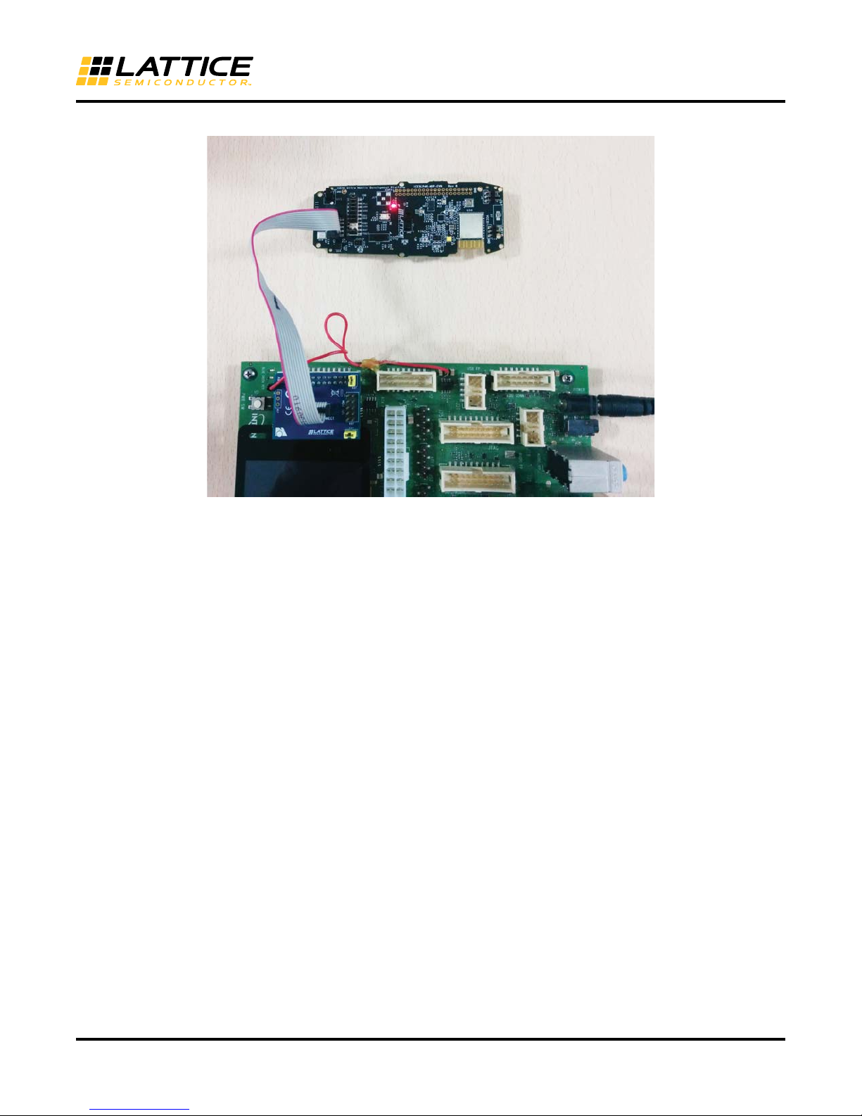
The board can be interface to external systems by one of two methods:
• SPI based application processor interface via J16 (AP Conn)
• BLE wireless module
For DragonBoard based SPI based application processor interfacing, a DragonBoard interfacing module and a
connecting ribbon cable are required (provided). Figure 5 shows the interfacing module, connecting cable, and
method to power the module from the DragonBoard.
A BLE module provides a feature on the board for wireless interfacing using Bluetooth Low energy version 4.
8
Page 9
iCE40 Ultra Mobile Development Platform User Guide
Figure 5. Data and 5 V Wiring from DragonBoard to DB Interface Module
Clocking
The board features an onboard 27 MHz oscillator. When an external clock is required, the SMA footprint can be
populated with a suitable SMA SMD connector (such as Molex part # 732511350). You must depopulate R51 on
the board.
Daisy Chain Interconnect / Expansion Connector
Daisy chain interconnect to the iCE FPGA by means of a connecting cable between two boards is possible via J10
on the main board. Refer to the schematics for the pin assignments of J10. All the pins of the FPGA are accessible
on this connector – and hence also forms a convenient way to tap into, or expand from any pin on the FPGA.
Basic Usage Procedures
Powering the Board
The board may be powered using one of three following methods:
• USB cable: USB A to mini B cable (supplied) connected to a PC may be used to power the board
• +5 V supplied to the DragonBoard interface module used to power the board through the provided ribbon cable.
The +5 V can be tapped from the DragonBoard as indicated in the Figure 5.
• Internal rechargeable battery not supplied with the kit. It must be procured separately. An example is the Nokia
BL-5C Lithium-ion battery shown in Figure 7.
Charging the Battery
The battery is charged when USB power is applied. Glowing of the green LED D3 (CHG) indicates the charging of
the battery. Glowing of the green LED D4 (EPW) indicates that an external charging power (USB) is applied. Glowing D3 indicates that charging is in progress. If D3 does not glow and D4 (EPW) glows, it means that charging is
complete.
9
Page 10

iCE40 Ultra Mobile Development Platform User Guide
Figure 6. USB Socket Located on the Lower Side
Figure 7. Nokia BL-5C Li-ion Battery Mounted Inside Back-cover of the Main Unit
Configuring the FPGA
The iCE40 Ultra can be configured using one of two methods:
• By programming the on-board SPI Flash U3 (ST Micro's M25P80)
• By directly configuring the FPGA using a processor to configure via iCE40 Ultra's SPI
Configuration by Programming SPI Flash
The SPI Flash (M25P80) can be programmed using the on-board FTDI's FT2232H (USB-SPI FIFO) via USB and
Lattice Diamond
To program the SPI Flash via USB and Lattice Diamond
1. Apply a jumper to FLCS on jumper pool header J15.
2. Connect the USB cable to the demo board.
3. Download the bitstream in SPI Flash (M25P80) using Lattice Diamond Programmer. To download the bitstream:
®
Programmer.
Programmer:
a. Open Diamond Programmer version 3.2 or above and select Create a new blank project as shown in
Figure 8.
10
Page 11

iCE40 Ultra Mobile Development Platform User Guide
Figure 8. Diamond Programmer Getting Started Dialog Box
b. The Diamond Programmer main interface opens, as shown in Figure 9.
Figure 9. Diamond Programmer Main Interface
c. Select iCE5LP in Device Family and iCE5LP4K in Device, as shown in Figure 10.
11
Page 12

Figure 10. Device Selection
iCE40 Ultra Mobile Development Platform User Guide
d. Double-click Fast Program and choose the desired *.bin file.
e. In the Device properties dialog box, select the program to be used in programming the device and click
OK, as shown in Figure 11.
Figure 11. Device Properties Dialog Box
12
Page 13

e. Verify that the operation is completed successfully. In the main interface, INFO: Operation: successful
is displayed in the Output pane.
Figure 12. Verifying Operation
iCE40 Ultra Mobile Development Platform User Guide
Alternatively, the SPI Flash can be programmed using Totalphase's Aardvark or Cheetah. Flash Center GUI flash
programming utility can be hooked up to the J29 (SPI PGM) header on the DragonBoard interfacing module.
To program the SPI Flash using Aardvark/Cheetah:
1. Apply a jumper on FLCS located on jumper pool header J15.
2. Ensure that the ribbon cable is connected between J16 (AP CONN) on main board and J26 (AP Interconnect)
on the DragonBoard interfacing module.
3. Remove shunt on J20 (PGM) header on the DragonBoard interfacing module.
4. Connect Aardvark / Cheetah to the J29 (SPI PGM) header on the DragonBoard interfacing module and its USB
to the PC/Laptop running the Flash Center GUI utility.
5. While operating the CRST button or applying the jumper on CRST of J15 (on the main board), use the Flash
Center GUI and appropriate bitmap to program the M25P80 SPI Flash.
6. After programming, remove the shunts on CRST and PGM.
Direct Configuration by a Processor (Processor Configuration)
The iCE40 Ultra FPGA can be configured directly without using an external SPI Flash. This can be done by the
application processor interfacing with the iCE40 Ultra SPI lines. While using this method appropriate software and
Android Application is required.
To configure the hardware:
1. Remove the jumper shunt on FLCS located on J15 (jumper pool header).
2. Apply a jumper shunt on FTRST located on J15 (jumper pool header).
3. Remove the jumper shunt on CRST located on J15 (jumper shunt header).
13
Page 14

iCE40 Ultra Mobile Development Platform User Guide
4. Using the ribbon cable provided, connect the main PCB and the DragonBoard through the DragonBoard inter-
facing module.
5. Run the appropriate software / application to configure iCE40 Ultra directly from the DragonBoard processor.
Current Measurements
FPGA currents are measured by inserting ammeters in series with the respective current paths. This is achieved by
means of removing the jumper shunts on the pooled jumper header J15, and replacing those by ammeters. Note
the legends printed across each of the jumpers on the PCB and the corresponding wiring in the schematics around
region of J15 to make the desired measurements. Current measurements for the high power LED (IR or white) can
be done at J9 (LED selecting 3 pin jumper). Note that RGB LED current measurements on J15 (jumper pool
header) is for the common Anode limb of the LED and not individual RGB circuits; Thus appropriate drive must be
made to measure individual RG
Technical Support Assistance
Submit a technical support case via www.latticesemi.com/techsupport
Revision History
Date Version Change Summary
June 2015 1.1 General update in multiple sections.
Updated Appendix A. Schematic Diagrams section.
Added Appendix B. Bill of Materials section.
June 2014 01.0 Initial release.
© 2015 Lattice Semiconductor Corp. All Lattice trademarks, registered trademarks, patents, and disclaimers are as
listed at www.latticesemi.com/legal. All other brand or product names are trademarks or registered trademarks of
their respective holders. The specifications and information herein are subject to change without notice.
14
Page 15

iCE40 Ultra Mobile Development Platform User Guide
5
5
4
4
3
3
2
2
1
1
D
D
C
C
B
B
A A
PRESSURE SENSOR
LATTICE SEMICONDUCTOR CORPORATION CONFIDENTIAL
Notes:
- Gyro and Accelerometer interfaces are both set to I2C
- I2C address LSB for both Gyro and Accelerometer is '1'
- SPI for both Gyro and Accelerometer is disabled
R
O
SNES LLA
H
ROS
N
ES RETEM
O
REL
E
CCA & EP
O
C
S
O
R
YG
RGB ALS SENSOR
PROXIMITY SENSOR-2
iCE5LP Mobile Development Platform Rev B
DEFAULT VCCIO1 IS SET TO 3.3V
poolA_sensor_SCL
poolA_sensor_SDA
poolA_sensor_SDA
poolA_sensor_SCL
poolA_sensor_SDA
poolA_sensor_SCL
Hall_out
poolA_sensor_SDA
poolA_sensor_SCL
VCCIO1
VCCIO1
VCCIO1
VCC3V3
VCCIO1
VCCIO1
VCCIO1
VCCIO1
poolA_sensor_SDA [Pg7]
poolA_sensor_SCL [Pg7]
Hall_out [Pg7]
Title
veRrebmuN tnemucoDeziS
t
ee
h
S
:
e
taD
of
04130-973-2
0
1
Pool-A I2C Sensors
B
210
Wednesday, April 22, 2015
Title
veRrebmuN tnemu
c
o
D
eziS
teehS
:etaD
of
04130-973-2
0
1
Pool-A I2C Sensors
B
210
Wednesday, April 22, 2015
Title
veRrebmuN tnemu
c
o
D
eziS
teehS
:etaD
of
04130-973-2
0
1
Pool-A I2C Sensors
B
210
Wednesday, April 22, 2015
R9
DNP
C25
0.1u
J14
ASCL
1
J13
ASDA
1
C79
1u
C57
1u
U18
MAX44008
VDD
1
GND
2
A0
3
INT4SCL5SDA
6
U22
BMP180
NC1
1
VDD
2
VDDIO
3
NC4
4
SCL
5
SDA
6
GND
7
R8
10k
U13
BU52051NVX
OUT
1
GND
2
NC3VDD
4
TPAD
5
C14
0.1u
U5
LSM330DLC
RES0
2
GND0
1
RES8
14
RES7
13
RES6
12
RES5
11
RES4
10
VDD0
7
CAP15DEN_G16DRDY_G/INT2_G
17
INT1_G18INT2_A19INT1_A
20
VDD_IO_0
21
CS_G
22
CS_A
23
SCL_A/G
24
VDD_IO_1
25
SDO_G
26
RES13RES2
4
RES3
5
GND1
6
VDD1
8
VDD2
9
SDO_A
27
SDA_A/G
28
C56
1u
R42
4k7
R3310k
C11
10u
TMD27711
U16
VDD1GND
3
LEDA
4
SCL
2
LEDK
5
LDR
6
INT
7
SDA
8
C16
10n
R41
4k7
C53
10u
C50
0.1u
C77
0.1u
C59
1u
Appendix A. Schematic Diagrams
Figure 13. Pool-A I2C Sensors
15
Page 16

iCE40 Ultra Mobile Development Platform User Guide
5
5
4
4
3
3
2
2
1
1
D
D
C
C
B
B
A A
Humidity, Temperature Sensor
IR RX MODULE
CLOCK OSCILLATOR
LATTICE SEMICONDUCTOR CORPORATION CONFIDENTIAL
PROXIMITY SENSOR-1COMPASS SENSOR
iCE5LP Mobile Development Platform Rev B
DEFAULT VCCIO2 IS SET TO 3.3V
poolB_sensor_SDA
poolB_sensor_SCL
poolB_sensor_SCL
poolB_sensor_SDA
GND
poolB_sensor_SCL
poolB_sensor_SDA
VCCIO2
VCCIO2
VCCIO2
VCCIO2
VCC3V3
VCCIO2
VCCIO2
poolB_sensor_SDA [Pg7]
poolB_sensor_SCL [Pg7]
IR_IN [Pg7]
clk [Pg7]
clk_stndby# [Pg7]
Title
v
e
RrebmuN
tnemucoD
e
ziS
te
eh
S:e
taD
of
04130-973-2
0
1
Pool-B I2C Sensors, IR Rx & Clocking
B
310
Wednesday, April 22, 2015
Title
veRrebmuN tnemu
c
o
D
eziS
teehS
:etaD of
04130-973-2
0
1
Pool-B I2C Sensors, IR Rx & Clocking
B
310
Wednesday, April 22, 2015
Title
veRrebmuN tnemu
c
o
D
eziS
teehS
:etaD of
04130-973-2
0
1
Pool-B I2C Sensors, IR Rx & Clocking
B
310
Wednesday, April 22, 2015
R2910k
ASFLMB-27.000MHZ-LC-T
U21
GND2VDD
4
STDBY#
1
OUT
3
R3
4k7
C5
1u
C55
1u
C76
0.1u
C1
0.1u
TMD27711
U15
VDD1GND3LEDA
4
SCL
2
LEDK
5
LDR
6
INT
7
SDA
8
R5
4k7
C49
4.7u
C58
10u
U14
SHT20
SDA
1
VSS
2
NC13NC2
4
VDD
5
SCL
6
PAD
7
C52
0.1u
U11
TSMP58000
VDD
3
OUT
1
GND
2
J2
BSCL
1
C6
0.1u
R43
10k
J1
BSDA
1
R22
100
C8
0.22u
C15
4.7u
LSM303DLHC
U4
C1
6
RES110RES211SETP12SETC
13
SCL
2
SDA
3
INT24INT1
5
DRDY
9
VDDIO
1
VDD
14
GND
7
NC
8
C51
1u
Figure 14. Pool-B I2C Sensors, IR Rx and Clocking
16
Page 17

Figure 15. Interconnects
5
5
4
4
3
3
2
2
1
1
D
D
C
C
B
B
A A
To jumper pool
Default: Shunt
Note position of pin#1
in reference board
SPI CONFIGURATION / FLASH
iCE5LP Mobile Development Platform Rev B
LATTICE SEMICONDUCTOR CORPORATION CONFIDENTIAL
SEEED BLE MODULE
AP INTERCONNECT
flsh_sclk
flsh_csproc_intr
proc_cs
CRSTb
ice_SOice_SI
flsh_mosi ice_SI
flsh_miso
ice_SO
flsh_sclk
flsh_miso
UART_TX
UART_RX
DRGN5V
VCCIO1
VCC3V3
VCC3V3
VCC3V3
ice_SO [Pg4,7]
proc_cs [Pg7]
flsh_cs [Pg4,5,7]
ice_SI[Pg4,7]
flsh_sclk[Pg4,5,7]
proc_intr
[Pg7]
CRSTb[Pg4,5,7]
flsh_miso [Pg5]
M25P80_CSn[Pg7]
flsh_mosi[Pg5]
UART_TX
[Pg7]
UART_RX
[Pg7]
CDONE [Pg5,7]
CRSTb[Pg4,5,7]
ice_SI[Pg4,7]
ice_SO[Pg4,7]
flsh_cs[Pg4,5,7]
flsh_sclk[Pg4,5,7]
SWCLK
[Pg7]
SWDIO[Pg7]
Title
v
e
RrebmuN
tnemucoDeziS
t
e
eh
S
:
e
taD
of
04130-973-2
0
1
INTERCONNECTS
B
410
Wednesday, April 22, 2015
Title
veRrebmuN tnemu
c
o
D
eziS
teehS
:etaD of
04130-973-2
0
1
INTERCONNECTS
B
410
Wednesday, April 22, 2015
Title
veRrebmuN tnemu
c
o
D
eziS
teehS
:etaD of
04130-973-2
0
1
INTERCONNECTS
B
410
Wednesday, April 22, 2015
R2
10k
R13
0
R68
0
DNP
R12
0
R78
820
J16
AP INTERCONNECT
2
4
6
8
10
1
3
579
D14
RED
Manufacturer = Osram
PART_NUMBER = LS L29K-G1J2-1-Z
DNP
12
R37 0
R35
0
R6
10k
R67
0
DNP
R7
10k
J18
BLE PROG SEL
1
2
3
R76
0
DNP
R45
0
DNP
R48
0
DNP
M25P80
U3
SDI5SCK
6
WP3CS
1
SDO
2
HOLD
7
8
VCC
4
GND
R77
0
DNP
C9
0.1u
C17
0.1u
U30
SeeedBLE
GND1SWCLK
2
SWDIO
3
VCC
4
p12
6
p135p117p9
9
p8
10
p7
11
p6
12
p5
13
p4
14
p3
15
p2
16
p1
17
p0
18
p2920p2821p25
22
p2423p23
24
p17
25
p18
26
GND
27
p10
8
p30
19
R4
10k
R75
0
DNP
R40
0
iCE40 Ultra Mobile Development Platform User Guide
17
Page 18

Figure 16. USB Programming and Power
5
5
4
4
3
3
2
2
1
1
D
D
C
C
B
B
A A
LATTICE SEMICONDUCTOR CORPORATION CONFIDENTIAL
iCE5LP Mobile Development Platform Rev B
FTDI PROGRAMMER
USB - POWER & PROGRAMMING
USB_DM
GND
FT_CRST
EP_CS
FT_CRST
GND
EP_DI
GND
EP_CLK
EP_CS
GND
FT_DI
FT_DI
FT_SK
FT_SK
FT_CS
EP_DI
FT_DO
FT_CS
EP_CLK
GND
USB_DP
GND
FT_DO
GND
GND
USB_DP
USB_DM
FT_CDONE
FT_CDONE
VCC3V3
VCC3V3
VCC3V3
FTVCOR
VCC3V3
FTVCOR
VCC3V3
FTVCOR
FTVCOR
VCC3V3
VCC3V3
VCC3V3
USB5V
CRSTb[Pg4,7]
flsh_miso
[Pg4]
flsh_sclk[Pg4,7]
flsh_cs[Pg4,7]
flsh_mosi
[Pg4]
CDONE
[Pg4,7]
FTRSTn[Pg7]
Title
veR
r
eb
muN
t
ne
mucoD
e
z
i
S
te
eh
S:etaD
of
04130-973-2
0
1
USB Programming & Power
B
510
Wednesday, April 22, 2015
Title
veRrebmuN tnemu
c
o
D
eziS
teehS
:etaD of
04130-973-2
0
1
USB Programming & Power
B
510
Wednesday, April 22, 2015
Title
veRrebmuN tnemu
c
o
D
eziS
teehS
:etaD of
04130-973-2
0
1
USB Programming & Power
B
510
Wednesday, April 22, 2015
R250 C13
0.1u
C37
27p
C48
0.1u
C30
4.7u
C22
0.1u
C47
0.1u
Y1
12MHz
R210
R23
470
5V D- D+ ID G
USB PWR
J5
1
2
3
4
S2
5
S1
S3
S4
R201k
R16 10
C23
27p
C21
10u
R11
10k
R260
C20
0.1u
L3
600 ohm, 500 mA
R280
R270
L1
600 ohm, 500 mA
R18
12k
93LC56BT-I/OT
U6
GND
2
VCC
6
DO
1
DI
3
CLK
4
CS
5
C29
0.1u
L2
600 ohm, 500 mA
C18
47u
C19
0.1u
R24
0
U9
FT2232H
Gnd_11OSCI2OSCO3VPHY4Gnd_75REF
6
DM
7
DP8VPLL
9
AGnd
10
Gnd11VCORE_112TEST13RESET#14Gnd_215ADBUS0
16
ADBUS1
17
ADBUS2
18
ADBUS3
19
VCCIO
20
ADBUS4
21
ADBUS5
22
ADBUS6
23
ADBUS7
24
Gnd_3
25
ACBUS0
26
ACBUS1
27
ACBUS2
28
ACBUS3
29
ACBUS4
30
VCCIO_3
31
ACBUS5
32
ACBUS633ACBUS7
34
Gnd_4
35
SUSPEND#
36
VCORE
37
BDBUS038BDBUS139BDBUS240BDBUS3
41
VCCIO_2
42
BDBUS443BDBUS544BDBUS645BDBUS7
46
Gnd_5
47
BCBUS0
48
VREGOUT
49
VREGIN
50
Gnd_6
51
BCBUS1
52
BCBUS2
53
BCBUS3
54
BCBUS4
55
VCCIO_1
56
BCBUS5
57
BCBUS6
58
BCBUS7
59
PWREN#
60
EEDATA
61
EECLK
62
EECS
63
VCORE_3
64
R102k2
C44
0.1u
C24
0.1u
R17 10
C38
0.1u
C43
4.7u
iCE40 Ultra Mobile Development Platform User Guide
18
Page 19

iCE40 Ultra Mobile Development Platform User Guide
5
5
4
4
3
3
2
2
1
1
D
D
C
C
B
B
A A
LATTICE SEMICONDUCTOR CORPORATION CONFIDENTIAL
FINGERPRINT SENSOR
I2S MICROPHONES - 2
iCE5LP Mobile Development Platform Rev B
FP_CS
I2S_SD1
I2S_SD2
VCCIO0
VCCIO2
VCC1V8
VCCIO2
VCCIO2
VCCIO2
I2S_LR1 [Pg7]
I2S_WS1 [Pg7]
I2S_SD1 [Pg7]
I2S_SCK1 [Pg7]
I2S_CE1 [Pg7]
I2S_CE2 [Pg7]
FP_MISO [Pg7]
FP_CS [Pg7]
FP_INTR [Pg7]
FP_SCK [Pg7]
FP_MOSI [Pg7]
I2S_LR2 [Pg7]
I2S_WS2 [Pg7]
I2S_SD2 [Pg7]
I2S_SCK2 [Pg7]
FP_RSTn[Pg7]
Title
veR
re
b
muN
tn
e
mucoD
e
z
i
S
te
eh
S:etaD
of
04130-973-2
0
1
I2S MIC, FINGERPRINT SENSORS and MICRO SD
B
610
Wednesday, April 22, 2015
Title
veRrebmuN tnemu
c
o
D
eziS
teehS
:etaD of
04130-973-2
0
1
I2S MIC, FINGERPRINT SENSORS and MICRO SD
B
610
Wednesday, April 22, 2015
Title
veRrebmuN tnemu
c
o
D
eziS
teehS
:etaD of
04130-973-2
0
1
I2S MIC, FINGERPRINT SENSORS and MICRO SD
B
610
Wednesday, April 22, 2015
R62
10k
R66
100k
R73
100k
R63
10k
D6
TVS/VAR
C66
0.1u
U19
ADMP441
SCK
1
SD
2
WS
3
LR
4
GND
5
GND1
6
VDD7CE
8
GND2
9
C60
0.1u
FPC1080A
U17
DR11DR213DR317DR429TXOUT120TXOUT221ANATEST18ANATEST29TEST410TEST316TEST215TEST1
32
SPICLK
24
MISO26MOSI
25
CSN
6
RSTN
5
IRQ
4
VDD1
3
VDD2
19
VDDA
11
VDDIO
27
GND5
31
GND6
30
GND7
2
GND8
7
GND9
12
GND10
14
GND1
18
GND2
22
GND3
23
GND4
28
R30
100
C63
0.1u
R61
10k
U12
ADMP441
SCK
1
SD
2
WS
3
LR
4
GND
5
GND16VDD7CE8GND2
9
C36
0.1u
R34
10k
C54
0.1u
C46
0.1u
Figure 17. I2S MIC, Fingerprint Sensors and Micro SD
19
Page 20

iCE40 Ultra Mobile Development Platform User Guide
5
5
4
4
3
3
2
2
1
1
D
D
C
C
B
B
A A
500mA track
500mA track
500mA track500mA track
Default: Shunt 1,2 (for IR LED)
All 500mA traces
All 500mA traces
Note:
Place close
to DUT
LATTICE SEMICONDUCTOR CORPORATION CONFIDENTIAL
iCE5LP Mobile Development Platform Rev B
IR, RGB and HI-POWER LEDs
DAISY CHAIN INTERCONNECT
100mA track
De-populate when using SMA CLK
KEY & SOCKET HEADER
OPTIONAL SMA CLOCK
DNP
JUMPER POOL HEADER
100mA track100mA track
DONE CRST
ALTERNATE RGB LED
Note:
Place close
to DUT
Note:
Place close
to DUT
500mA track
500mA track
CRSTb
VCC_A5
RLED
RGB_Anode
GLED
BLED
IRLEDVLED
VLED
HPLED
IRLED
GPIO_B2
Hall_out
CDONE
SMA_CLK
GPIO_B5
BAR_LED
VCC_A5
VCCPLL_B3
VPP2V5_D4
SPIVCCIO1_C3
VCCIO0_A4
VCCIO2_C4
RGB_Anode
GPIO_A6
BLED
GPIO_B6
GLED
GPIO_C6
RLED
GPIO_D6
poolB_sensor_SCL
GPIO_D5
GPIO_E6 poolB_sensor_SDA
GPIO_E5 BAR_LED
GPIO_F6
GPIO_F5
IR_IN
flsh_cs
CRSTb
GPIO_E5
GPIO_B6
GPIO_B1
SPIVCCIO1_C3
VCCIO0_A4
GPIO_D6
GPIO_F5
poolA_sensor_SDA
proc_cs
VCC_A5
GPIO_B2
GPIO_E6
GPIO_A6
HPLED
UART_TX
GPIO_D2
flsh_cs
CRSTb
UART_RX
VCCPLL_B3
GPIO_F6
GPIO_C6
ice_SO
poolA_sensor_SCL
proc_intr
GPIO_D5
CDONE
flsh_sclk
VCCIO2_C4
CLK_F4
ice_SI
GPIO_B5
VPP2V5_D4
GND GND
GPIO_D6
BLED
GLED
RGB_Anode
RLED
SPIVCCIO1_C3
GPIO_B1
VCCPLL_B3
GND
GND
VCCIO2_C4
GPIO_B6
HPLED
GPIO_C6
GPIO_B2
poolA_sensor_SCL
poolA_sensor_SDA
VPP2V5_D4
CDONE
flsh_cs
flsh_sclk
ice_SO
ice_SI
CRSTb
GPIO_E5
GPIO_F5
GPIO_D5
proc_cs
proc_intr
GPIO_D6
GPIO_D2
GPIO_E6
CLK_F4
GPIO_F6
GPIO_B5
GPIO_A6
VCCIO0_A4
VCCIO1
VCC3V3HP
VCC3V3HP
VCCIO1
VCC1V2
VCC2V5
VCCIO1
VCCIO0
VCCIO2
VCC3V3HP
VCC3V3
flsh_cs
[Pg4,5]
Hall_out[Pg2]
CDONE[Pg4,5]
poolB_sensor_SDA[Pg3]
poolB_sensor_SCL[Pg3]
poolA_sensor_SDA[Pg2]
poolA_sensor_SCL[Pg2]
IR_IN[Pg3]
flsh_sclk[Pg4,5]
ice_SI
[Pg4]
proc_intr
[Pg4]
CRSTb[Pg4,5]
ice_SO
[Pg4]
proc_cs
[Pg4]
I2S_WS1 [Pg6]
FTRSTn [Pg5]
I2S_CE1
[Pg6]
I2S_SCK1 [Pg6]
I2S_SD1
[Pg6]
FP_SCK [Pg6]
I2S_SD2[Pg6] FP_CS [Pg6]
I2S_WS2 [Pg6]
FP_MOSI [Pg6]
I2S_SCK2[Pg6]
FP_INTR [Pg6]
I2S_LR2[Pg6]
FP_MISO [Pg6]
I2S_CE2[Pg6]
I2S_LR1 [Pg6]
M25P80_CSn [Pg4]
clk_stndby#[Pg3]
FP_RSTn[Pg6]
SWCLK
[Pg4]
SWDIO[Pg4]
UART_TXPg[4]
UART_RX
Pg[4]
clk
Pg[3]
Title
veRreb
m
uN tne
m
uco
D
eziS
te
eh
S:etaD
of
04130-973-2
0
1
iCE5LP4KSWG36 FPGA & LEDs
B
710
Wednesday, April 22, 2015
Title
veRrebmuN tnemu
c
o
D
eziS
teehS
:etaD of
04130-973-2
0
1
iCE5LP4KSWG36 FPGA & LEDs
B
710
Wednesday, April 22, 2015
Title
veRrebmuN tnemu
c
o
D
eziS
teehS
:etaD of
04130-973-2
0
1
iCE5LP4KSWG36 FPGA & LEDs
B
710
Wednesday, April 22, 2015
J7
KEY
2
468
1012141618
20
22
242628
30
1
3
57911131517
19
21
232527
29
3132
C70
10n
C71
10n
C65
10n
D5
VIS
1
K
2
A
3
3
J9
HP LED SEL
1
2
3
C72
1u
R38
2k2
C64
10n
C67
1u
C78
0.1u
J10
CON40A
1 2
3
4
5 6
7 8
9
101112
13 14
151617
18
19 20
21 22
23 24
25 26
27 28
29 30
31
32
33
34
35 36
37
38
39 40
J17
SMA
A
1
Sh12Sh2
3
Sh3
4
Sh4
5
C75
10n
R470
DNP
D8
BAR
D13
APTF1616SEEZGQBDC
A
1
R2G
3
B
4
R44
100
C90
0.1u
J15
A3-20PA-2SV(71)
1
3
5
7911
13
151719
2
4
6
8
101214
16
18
20
C62
1u
R14
150
R46
2k2
R740
R390
R49
10k
C61
0.1u
C69
0.1u
C73
0.1u
R51
0
C68
0.1u
Bank 0
Bank 2
CONFIG SPI & Bank 1
iCE5LP4KSWG36
iCE5LP4KSWG36
U20
IOB_2A_MISO_SPI2
F6
IOB_3B_G6_MOSI_SPI2
E6
IOB_4A_SCK_SPI2
D6
IOB_5B_MCSN0_SPI2
D5
IOB_6A
F5
IOB_7B
E5
IOB_29B
E2
IOB_30A
C1
IOB_31B
B2
IOB_32A_SO_MISO_SPI1
F2
IOB_33B_SI_MOSI_SPI1
D1
SPI_VCCIO1
C3
IOB_10A
B4
IOB_11B_G5
F4
CRESET_B
D3
IOB_16A
F3
IOB_20AE3IOB_25B_G3
C2
IOB_26A
B1
IOB_27B
D2
IOB_34A_SCK_SCK_SPI1
E1
IOB_35B_SS_MCSNO_SPI1
F1
VCCPLL
B3
IOT_46B_G0
B5
RGB2A6RGB1B6RGB0
C6
GND2
A3
GND1
C5
VCC
A5
VCCIO_0
A4
VCCIO_2
C4
VPP_2V5
D4
IOB_12A_G4_CDONE
E4
IRLED
A2
VSSIO_LED
A1
SW3
PB
D9
LED
C74
1u
D12
RGB
Green
1
Red2Anode
3
Blue
4
D7
IR
Figure 18. iCE5LP4KSWG36 FPGA and LEDs
20
Page 21

Figure 19. Power Supplies
5
5
4
4
3
3
2
2
1
1
D
D
C
C
B
B
A A
spread across board, easy access
Default: 3V3
LDO REGULATORS
CHARGER
3
V3 :
tl
uaf
eD
3
V3 :
tl
ua
feD
YELLOW
GREEN
s
e
ca
r
t Am0
0
5secart Am
0
05
500mA traces
iCE5LP Mobile Development Platform Rev B
LATTICE SEMICONDUCTOR CORPORATION CONFIDENTIAL
POWER SOURCE SELECTOR
PWR
VCC3V3
VCC2V5
VCC3V3
VCC2V5
VCC1V8 VCC1V8
LDO_CE_VDC
LDO_CE_VDC
VCCIO0
VDC
VCC1V2
VCC1V8
VCCIO1
VCC3V3
VCCIO2
VCC1V8
VCC2V5
VCC2V5
VCC3V3
VDC
VCC3V3
USB5V
VBAT
VCC3V3HP
VDC
VBAT
VDC
VDC
USB5V
DRGN5V
Title
v
e
RrebmuN
tnemucoD
e
ziS
tee
h
S:e
t
a
D
of
04130-973-2
0
1
Power Supplies
B
810
Wednesday, April 22, 2015
Title
veRrebmuN tnemu
c
o
D
eziS
teehS
:etaD of
04130-973-2
0
1
Power Supplies
B
810
Wednesday, April 22, 2015
Title
veRrebmuN tnemu
c
o
D
eziS
teehS
:etaD of
04130-973-2
0
1
Power Supplies
B
810
Wednesday, April 22, 2015
BC1
Bat connector
VIN1GND
3
NC25NC1
4
NTC
2
MH16MH2
7
R59DNP
AP7312-1218FM-7
U10
1.8VO
5
1.8EN
3
1.2EN
2
1.2VO
6
VIN
1
GND
4
EPAD
7
C2
1u
R60DNP
J11
GND
1
D1
PMEG2010AEH
C3
2.2u
R580
J12
GND
1
C4
10u
C35
10u
R31
1k
R1
5k6
C26
0.1u
C40
10u
C28
0.1u
C42
10u
C45
10u
C7
10u
R32
1k
U1 MC34673AEPR2
VIN1nPPR
2
nCHG
3
nEN
4
BAT
8
ISET
7
nFAST
6
GND
5
EPAD
9
C31
10u
C41
10u
D10
LED
U7
LTC4411
In
1
Gnd
2
Ctl
3
Stat
4
Out
5
R520
U8
XC6222B331MR-G
Vin
1
Vss
2
CE
3
NC
4
Vout
5
J3
GND
1
D4
LED
R50
1k
R53DNP
C33
0.1u
C12
0.1u
D2
PMEG2010AEH
R54DNP
U2
MIC5335-SJYMT
VIN
1
GND
2
2V5EN
3
3V3EN
4
2V5VO
5
3V3VO
6
PAD
7
D3
LED
SW2
PWR
C34
10u
R550
R19
1k
C10
47u
R56DNP
C39
0.1u
C32
0.1u
R57DNP
C27
10u
iCE40 Ultra Mobile Development Platform User Guide
21
Page 22

Figure 20. Keys (4 Different PCB Modules)
5
5
4
4
3
3
2
2
1
1
D
D
C
C
B
B
A A
KEY-A (DEFAULT) KEY-B (GETS FP ILO PoolB)
KEY-C (GETS I2S MICs ILO PoolB, IR Rx, RGB)
KEY-D (CUSTOM KEY)
iCE5LP Mobile Development Platform Rev B
LATTICE SEMICONDUCTOR CORPORATION CONFIDENTIAL
Title
v
e
RrebmuN
tnemucoD
e
ziS
tee
h
S:e
t
a
D
of
04130-973-2
0
1
KEYS (4 different PCB modules)
B
910
Wednesday, April 22, 2015
Title
veRrebmuN tnemu
c
o
D
eziS
teehS
:etaD of
04130-973-2
0
1
KEYS (4 different PCB modules)
B
910
Wednesday, April 22, 2015
Title
veRrebmuN tnemu
c
o
D
eziS
teehS
:etaD of
04130-973-2
0
1
KEYS (4 different PCB modules)
B
910
Wednesday, April 22, 2015
J23
CON15
123456789101112131415
J4
DF12B(3.0)-30DP-0.5V(86)
246
8
101214161820222426
28
30
135791113151719212325
27
29
3132
J6
DF12B(3.0)-30DP-0.5V(86)
246
8
10
1214161820
22
24
262830
135791113151719212325
27
29
3132
J8
DF12B(3.0)-30DP-0.5V(86)
2
468
10
121416
182022
242628
30
1357911131517192123252729
3132
J21
DF12B(3.0)-30DP-0.5V(86)
246
8
10121416182022
242628
30
13579111315171921
232527
29
3132
J22
CON15
123456789
1011121314
15
iCE40 Ultra Mobile Development Platform User Guide
22
Page 23

iCE40 Ultra Mobile Development Platform User Guide
5
5
4
4
3
3
2
2
1
1
D
D
C
C
B
B
A A
DNP
MISO FOR iCE,
MOSI FOR FLASH
MISO FOR iCE,
MOSI FOR FLASH
DNP
iCE5LP Mobile Development Platform Rev B
LATTICE SEMICONDUCTOR CORPORATION CONFIDENTIAL
SPI_CS_1V8
INTRV_1V8
SPI_CLK_1V8
SPI_MOSI_1V8
SPI_MISO_1V8
SPI_CS
SPI_MISO
SPI_CLK
SPI_MOSI
VCC5VLT
INTRV
VCC5VLT
CReset1V8
GPIO_CS_1V8
CReset3V3
SPI_MOSI_1V8
VCCBVLT
SPI_CLK_1V8
SPI_MISO_1V8
SPI_MISO
SPI_MOSI
SPI_CLK
GPIO_PROC_CS
GPIO_PROC_CS
SPI_CLK SPI_MISO
SPI_MOSI
SPI_CS_1V8
CS
CS
GPIO_CS_1V8
CS
VLTOE
CReset1V8
VCCBVLT
SPI_CS_1V8
INTRV_1V8
CReset3V3
SPI_CS
SPICS3V3
INTRV
VLTOE
SPICS3V3
GPIO_PROC_CS
VCC1V8V
VCC3V3V
VCC1V8V
VCC1V8V
VCC3V3VVCC1V8V
VCC5VLT
VCC1V8V
VCC1V8V
VCC1V8V
Title
v
e
RrebmuN
tnemucoD
e
ziS
tee
h
S:e
t
a
D
of
0413
0
-B973-2
0
1
DragonBoard VLT Adapter module
B
10 10
Wednesday, April 22, 2015
Title
veRrebmuN tnemu
c
o
D
eziS
teehS
:etaD of
0413
0
-B973-2
0
1
DragonBoard VLT Adapter module
B
10 10
Wednesday, April 22, 2015
Title
veRrebmuN tnemu
c
o
D
eziS
teehS
:etaD of
0413
0
-B973-2
0
1
DragonBoard VLT Adapter module
B
10 10
Wednesday, April 22, 2015
U23
74AVC4T774
DIR11DIR2
2
A1
3
A24A35A4
6
DIR3
7
DIR4
8
OE
9
GND
10
B411B3
12
B213B1
14
VCCB15VCCA
16
C84
0.1u
J20
PRGM
1
2
C89
0.1u
C88
0.1u
R64
0
J24
SPICS
1
2
C82
10u
R65
DNP
J26
10p 2mm
2
4
6
1
3
578910
C118
0.1u
R69
0
J29
Aardvark Header
SS2
1
GND1
2
SS3
3
NC2
4
MISO
5
NC1
6
SCLK
7
MOSI
8
SS1
9
GND2
10
C80
10u
C85
0.1u
R71 10k
U24
LD1117-3V3
GND
1
VOUT
2
VIN
3
4
TAB
C86
10u
TP10
+5V
1
R72
0
C119
0.1u
DNP
J27
24p 2p54mm
13579111315171921
23
246
8
10
121416
18
202224
U29
74AVC4T774
DIR11DIR2
2
A1
3
A24A3
5
A4
6
DIR37DIR4
8
OE
9
GND
10
B4
11
B312B2
13
B1
14
VCCB
15
VCCA
16
U25
LD1117-1V8
GND
1
VOUT
2
VIN
3
TAB
4
R70 10k
J28
1
2
3
C83
0.1u
C81
10u
U26
SN74AUP1G08DBVR
A1B
2
GND
3
Y
4
VCC
5
C87
0.1u
Figure 21. DragonBoard VLT Adapter Module
23
Page 24

iCE40 Ultra Mobile Development Platform User Guide
Appendix B. Bill of Materials
Item Reference Quantity Part PCB Footprint Comments Par t Num ber Manufacturer Description
1 BC1 1 Bat connector BATT_009155003
2 C1,C6,C9,C12,C13,C14,C17,
3 C2,C5,C51,C55,C56,C57,C59,
4 C3 1 2.2 u C0603 — CC0603ZRY5V6
5 C4,C11,C21,C27,C31,C35,C4
6 C7,C34,C41,C42,C80,C86 6 10 u C0603 — CL10X106MP8N
7 C8 1 0.22 u C0603 — CL10B224KO8N
8 C10,C18 2 47 u C3528 — TCJB476M010R
9 C15,C30,C43,C49 4 4.7 u C0603 — CC0603KRX5R6
10 C16,C64,C65,C70,C71,C75 6 10 n C0402 — CL05B103KO5N
11 C23,C37 2 27 p C0402 — CL05C270JB5N
12 C119 1 0.1 u C0402 DNP CL05A104MP5N
13 D1,D2 2 PMEG2010AEH SOD123F — PMEG2010AEH,
14 D3 1 LED led0603 — LG L29K-G2J1-
15 D4 1 LED led0603 — LY Q976-P1S2-36Osram Opto LED CHIPLED 587NM YLW 0603 SMD
C19,C20,C22,C24,C25,C26,
C28,C29,C32,C33,C36,C38,
C39,C44,C46,C47,C48,C50,
C52,C54,C60,C61,C63,C66,
C68,C69,C73,C76,C77,C78,
C83,C84,C85,C87,C88,C89,
C90,C118
C62,C67,C72,C74,C79
0,C45,C53,C58,C81,C82
45 0.1 u C0402 — CL05A104MP5N
12 1 u C0402 — CL05A105KP5N
12 10 u C0603 — CL10A106MQ8
301006
— 09155003301006AVX CONN BATTERY 3 POS RIGHT
NNC
NNC
BB225
NNNC
RNC
NNC
0070
BB475
CNC
NNC
NNC
115
24-Z
Samsung CAP CER 0.1UF 10V 20% X5R 0402
Samsung CAP CER 1UF 10V 10% X5R 0402
Ya g e o CAP CER 2.2UF 10V Y5V 0603
Samsung CAP CER 10UF 6.3V 20% X5R 0603
Samsung CAP CER 10UF 10V 20% X6S 0603
Samsung CAP CER 0.22UF 16V 10% X7R 0603
AVX CAP TANT 47UF 10V 20% 1210
Ya g e o CAP CER 4.7UF 10V 10% X5R 0603
Samsung CAP CER 10000PF 16V 10% X7R
Samsung CAP CER 27PF 50V 5% NP0 0402
Samsung CAP CER 0.1UF 10V 20% X5R 0402
NXP Semiconductor
Osram Opto LED SMARTLED GREEN 570NM
ANGLE
0402
DIODE SCHOTTKY 20V 1A SOD123F
0603
16 D5 1 VIS XBDAWT — XBDAWT-00-
17 D6 1 TVS/VAR R0603 — VC060330A650DPAVX VARISTOR 36.9V 30A 0603
18 D7 1 IR IRD — VSMB2948SL Vishay IR EMITTER HIGH SPEED 940NM
19 D8 1 BAR LED0805 — APT2012SRCPRVKingbright Corp LED 2X1.2MM 640NM RD WTR CLR
20 D9 1 LED led0603 — LG L29K-G2J1-
21 D10 1 LED led0603 — LS Q976-NR-1 Osram Opto LED CHIPLED 633NM RED 0603 SMD
22 D12 1 RGB RGBD DNP AEBMTRGBZ Custom —
23 D13 1 APTF1616SEEZ
24 D14 1 RED LED0603 DNP LS L29K-G1J2-
25 J1 1 BSDA TP_TH_40_24_S DNP PCB MDN —
26 J2 1 BSCL TP_TH_40_24_S DNP PCB MDN —
27 J3,J11,J12 3 GND TUR_TH DNP 1573-2 Keystone Elec-
28 J4,J6,J8,J21 4 DF12B(3.0)-
29 J5 1 USB PWR CONN_S5P1RMI
30 J7 1 KEY HIROSE_DF12B_30— DF12B(3.0)-
31 J9 1 HP LED SEL hdr1x3-40_2mm — NRPN031PARN-RCSullins Connec-
32 J10 1 CON40A hdr20x2_2mm DNP 0877582016 Molex Inc CONN HEADER 20POS 2MM VERT
33 J13 1 ASDA TP_TH_40_24_S DNP PCB MDN —
GQBDC
30DP-0.5V(86)
RGBOPT2 — APTF1616SEEZ
HIROSE_DF12B_
30_mirror
NIUSBB_MOLEX
000000000LCE3
24-Z
GQBDC
1-Z
— DF12B(3.0)-
30DP-0.5V(86)
— 67503-1020 Molex CONN RECEPT MINIUSB R/A 5POS
30DS-0.5V(86)
Cree Inc LED HIGH BRIGHTNESS
SMD
SMD
Osram Opto LED SMARTLED GREEN 570NM
KingbrightCorp LED RED/GREEN/BLUE WTR CLEAR
Osram LED SMARTLED GREEN 570NM
tronics
Hirose CONN HEADER 30POS 3MM SMD
Hirose CONN RCPT 30POS 3MM SMD
tor Solutions
0603
SMD
0603
TERMINAL TURRET DBL .082"L
0.5MM
SMD
0.5MM
CONN HEADER 2MM SINGLE R/A
3POS
GOLD
24
Page 25

iCE40 Ultra Mobile Development Platform User Guide
Item Reference Quantity Part PCB Footprint Comments Part Number Manufacturer Description
34 J14 1 ASCL TP_TH_40_24_S DNP PCB MDN —
35 J15 1 A3-20PA-
36 J16 1 AP INTERCON-
37 J17 1 SMA molex_0732511350DNP 732511350 Molex CONN SMA JACK STR 50 Ohm SMD
2SV(71)
NECT
hirose_10x2_2m
m
hirose_5x2_2mm — A3-10PA-
— A3-20PA-
2SV(71)
2SV(71)
Hirose CONN HEADER 20POS 2MM GOLD
Hirose CONN HEADER 10POS 2MM GOLD
SMD
SMD
38 J18 1 BLE PROG SEL hdr1x3-40_2mm — NRPN031PARN-RCSullins Connec-
39 J20 1 PRGM HDR1X2-40 — 77311-801-02LF FCI CONN HEADER .100 SINGL STR
40 J22,J23 2 CON15 HDR1x15_2mm_THDNP PCB MDN —
41 J24 1 SPICS HDR1X2-40 — 77311-801-02LF FCI CONN HEADER .100 SINGL STR
42 J26 1 10p 2 mm hdr_5x2_2mm — 0877581016 Molex Inc CONN HEADER 10POS 2MM VERT
43 J27 1 24p 2p 54 mm hdr12x2_TH_2p5
44 J28 1 DNP hdr1x3-40 DNP 77311-801-03LF FCI CONN HEADER .100 SINGL STR
45 J29 1 Aardvark Header hdr5x2 — 77313-801-10LF FCI CONN HEADER .100 SINGL STR
46 L1,L2,L3 3 600 Ohm,
47 R1 1 5k6 R0402 — RC1005F562CS Samsung RES 5.6 kOhm 1/16W 1% 0402
48 R2,R4,R6,R7,R8,R11,R29,
49 R3,R5,R41,R42 4 4k7 R0402 — RC1005J472CS Samsung RES 4.7 kOhm 1/16W 5% 0402
50 R9 1 DNP R0402 DNP WR04X000PTL Walsin —
51 R10,R38,R46 3 2k2 R0402 — RC1005J222CS Samsung RES 2.2 kOhm 1/16W 5% 0402
52 R12,R13,R35,R40 4 0 R0402 — RC1005J000CS Samsung RES 0.0 Ohm 1/16W JUMP 0402
53 R14 1 150 R0402 — RMCF0402JT150RStackpole Elec-
54 R16,R17 2 10 R0402 — RC1005J100CS Samsung RES 10 Ohm 1/16W 5% 0402
55 R18 1 12k R0402 — RC1005F123CS Samsung RES 12 kOhm 1/16W 1% 0402
56 R19,R20,R31,R32,R50 5 1k R0402 — RC1005J102CS Samsung RES 1 kOhm 1/16W 5% 0402
57 R21,R24,R25,R26,R27,R28,
58 R22 1 100 R0603 — RC1608J101CS Samsung RES 100 Ohm 1/10W 5% 0603
59 R23 1 470 R0402 — RC1005J471CS Samsung RES 470 Ohm 1/16W 5% 0402
60 R30,R44 2 100 R0402 — RC1005J101CS Samsung RES 100 Ohm 1/16W 5% 0402
61 R45,R47,R48,R67,R68,R75,
62 R53,R54,R56,R57,R59,R60,
63 R66,R73 2 100k R0402 — RC1005J104CS Samsung RES 100 kOhm 1/16W 5% 0402
64 R78 1 820 R0402 — RC1005F821CS Samsung RES SMD 820 Ohm 1% 1/16W 0402
65 SW2 1 PWR EG1218O_switch — EG1218 E-Switch SWITCH SLIDE SPDT 30V.2A PC
66 SW3 1 PB 2psmd_eswitch — TL1015AF160QGE-Switch SWITCH TACTILE SPST-NO 0.05A
67 TP10 1 +5 V HDR1 — 77311-801-01LF FCI HEADER BERGSTIK
68 U1 1 MC34673AEPR28-UDFN — MC34673AEPR2Freescale Semi-
69 U2 1 MIC5335-
70 U3 1 M25P80 SOIC8-W — M25P80-
71 U4 1 LSM303DLHC LGA14_LSM303 — LSM303DLHC ST Micro ACCELEROMETER/MAGNETOME-
72 U5 1 LSM330DLC LGA-28 — LSM330DLC ST Micro ACCELEROMETER/MAGNETOME-
73 U6 1 93LC56BT-I/OT SOT23-6 — 93LC56BT-I/OT Microchip Tech-
R33,R34,R43,R49,R61,R62,
R63,R70,R71
R37,R39,R51,R52,R55,R58,
R64,R69,R72,R74
R76,R77
R65
16 10k R0402 — RC1005J103CS Samsung RES 10 kOhm 1/16W 5% 0402
16 0 R0402 — RC1005J000CS Samsung RES 0.0 Ohm 1/16W JUMP 0402
8 0 R0402 DNP RC1005J000CS Samsung RES 0.0 Ohm 1/16W JUMP 0402
7 DNP R0402 DNP RC1005J000CS Samsung RES 0.0 Ohm 1/16W JUMP 0402
500 mA
SJYMT
4_mirror
L0603 — MMZ1608R601A TDK Corp FERRITE CHIP 600 Ohm 500MA 0603
6TMLF — MIC5335-
— M20-7831242 Harwin Inc 12+12 DIL VERT SOCKET L/FREE
SJYMT
VMW6G
tor Solutions
tronics
conductor
Micrel IC REG LDO 3.3 V/2.5 V 0.3A 6TMLF
Numonyx/ST
Micro
nology
CONN HEADER 2MM SINGLE R/A
3POS
2POS
2POS
GOLD
3POS
10POS
RES 150 Ohm 1/16W 5% 0402
MNT
12V
IC SGL CELL BATTERY CHRGR 8UDFN
IC FLASH 8MBIT 75MHZ 8SO
TER 14LGA
TER 28LGA
IC EEPROM 2KBIT 2MHZ SOT23-6
25
Page 26

iCE40 Ultra Mobile Development Platform User Guide
Item Reference Quantity Part PCB Footprint Comments Part Number Manufacturer Description
74 U7 1 LT C4 4 11 TSOT23-5 — LTC4411ES5#T
75 U8 1 XC6222B331MR-GSOT25 — XC6222B331MR-GTorex Semicon-
76 U9 1 FT2232H LQFP64 — FT2232HL FTDI IC USB HS DUAL UART/FIFO 64-
77 U10 1 AP7312-
78 U11 1 TSMP58000 TSOPIRx3P — TSMP58000 Vishay 3 V PH.MODULE S.VIEW
79 U12,U19 2 ADMP441 ADMP441 — INMP441ACEZ Invensense Omnidirectional Microphone with bot-
80 U13 1 BU52051NVX SSON004X1216 — BU52051NVX ROHM Semicon-
81 U14 1 SHT20 DFN6 — SHT20 Sensirion Humidity and Temperature Sensor IC
82 U15,U16 2 TMD27711 DFNL8 — TMD27711 AMS-TAOS USA
83 U17 1 FPC1080A FPC1080A — FPC1080A Fingerprints Swip e Sensor Package
84 U18 1 MAX44008 OTDFN-6 — MAX44008EDT+ Maxim Inte-
85 U20 1 iCE5LP4KSWG3636WLCSP Customer
86 U21 1 ASFLMB-
87 U22 1 BMP180 BMP180 — BMP180 Bosch SENSOR PRESSURE ABS
88 U23,U29 2 74AVC4T774 16TSSOP — SN74AVC4T774
89 U24 1 LD1117-3V3 sot223_ns — LD1117S33CTR ST Micro IC REG LDO 3.3 V 0.8A SOT223
90 U25 1 LD1117-1V8 SOT223_NS — LD1117AS18 ST Micro IC REG LDO 1.8 V 1A SOT223
91 U26 1 SN74AUP1G08
92 U30 1 SeeedBLE SeeedBLE — 113050012 Seeed Low cost ARM cortex-m0 based mod-
93 Y1 1 12 MHz 5x3p2mm2p — ABM3-
94 iCE40 Ultra MDP BOARD PCB 1 ———305-PD-15-0056 PAC T RO N —
BAG and TAG
Item Reference Qty Par t PCB Footprint Comments PA R T_ NUMBER Manufacturer Description
1 Battery 1 Li-ion Battery Battery unit - BL-5C Nokia From Amazon or other Nokia vendor
2 Plastic Enclosure 1 Plastic enclosure Plastic Enclosure Customer
3 SPI cable assembly 1 SPI cable
4 Fasteners / screws 2 PCB-Plastic fas-
5 2 mm jumper shunts for J15 7 2 mm jumper
6 2 mm jumper shunts with grip
7 2.54 mm jumper shunt for J20 1 2.54 mm jumper
for J15 & J9, J18
3 2 mm jumper
1218FM-7
27.000MHZ-LCT
DBVR
assembly
tening screws
shunts for J16
shunts with grip
for J15 and J10
shunt for J21
AP7312_6DFN — AP7312-
Supplied
osc_5x3p2 — ASFLMB-
SOT23-5 DNP SN74AUP1G08
Supplied
SPI cable assembly
PCB-Plastic fastening screws
2 mm jumper
shunts for J17
2 mm jumper
shunts with grip
for J15 and J11
2.54 mm jumper
shunt for J22
Customer
Supplied
BAG and
BAG and
BAG and
BAG and
RMPBF
1218FM-7
iCE5LP4KSWG36CTR
27.000MHZ-LCT
PWR
DBVR
12.000MHZ-B2T
Enclosure / full
housing set used
for Nokia 1110 **
Custom made or
Samtech part #
TCSD-05-D-
06.00-01-N
SMPPS0003 -
TAG
#0 x 3/16 - Pan
Head Sheet
Metal Screws –
Phillips
SPN02SYBN-RCSullins 2 mm jumper shunts for J15
TAG
NPN02SXLN-RCSullins 2 mm jumper shunts with grip for J15 &
TAG
STC02SYAN Sullins 2.54 mm jumper shunt for J20
TAG
Linear Technology
ductor Ltd
Diodes Inc IC REG LDO 1.2 V/1.8 V 0.15A 6DFN
ductor
Inc
grated
Lattice Semiconductor
ABRACON OSC MEMS 27.000MHZ CMOS SMD
Texas Instruments
Texas Instruments
Abracon Corp CRYSTAL 12MHZ 18PF SMD
Nokia or OEM From ebay or other Nokia accessory
Custom made or
equivalent Samtec Inc
Micro Fasteners SMPPS0003 - #0 x 3/16 - Pan Head
IC OR CTRLR SRC SELECT TSOT235
IC REG LDO 3.3 V 0.7A SOT25
LQFP
tom port and I2S digital port
IC LATCH SENSOR BIPO CMOS
4SSON
IC PROXIMITY DETECTOR DGTL 8MOD
IC AMBIENT/PROXIMITY SENS TDFN
—
IC BUS TRANSCVR 4BIT DL
16TSSOP
IC GATE AND 1CH 2-INP SOT-23-5
ule for Bluetooth module
vendor ** see note in comments
2 mm pitch, dual row, 5x2 FRC / IDC
female terminated, 15 cms ribbon
cable
Sheet Metal Screws – Phillips
J9
8 Jumper / Flywire for DB +5 V 1 Jumper / Flywire
for DB + 5 V
4” Jumper / Flywire for DB +5 V
26
Customer
Supplied
— Custom made or
equivalent
One side bare wire (28 or 26 AWG),
one side female header (single socket,
for 2.54 pitch type header)
Page 27

Mouser Electronics
Authorized Distributor
Click to View Pricing, Inventory, Delivery & Lifecycle Information:
Lattice:
ICE5LP4K-MDP-EVN
 Loading...