

1
10
11
20
I/CLK
I
I
I
I
I
I
I
I
GND
Vcc
I/O/Q
I/O/Q
I/O/Q
I/O/Q
I/O/Q
I/O/Q
I/O/Q
I/O/Q
I/OE
5
15
查询GAL16V8D供应商查询GAL16V8D供应商
GAL16V8/883
High Performance E2CMOS PLD
Generic Array Logic™
Features
• HIGH PERFORMANCE E2CMOS® TECHNOLOGY
— 7.5 ns Maximum Propagation Delay
— Fmax = 100 MHz
— 6 ns Maximum from Clock Input to Data Output
— TTL Compatible 12 mA Outputs
— UltraMOS
• 50% REDUCTION IN POWER FROM BIPOLAR
— 75mA Typ Icc
• ACTIVE PULL-UPS ON ALL PINS (GAL16V8D-7 and
GAL16V8D-10)
2
CELL TECHNOLOGY
•E
— Reconfigurable Logic
— Reprogrammable Cells
— 100% Tested/100% Y ields
— High Speed Electrical Erasure (<100ms)
— 20 Year Data Retention
• EIGHT OUTPUT LOGIC MACROCELLS
— Maximum Flexibility for Complex Logic Designs
— Programmable Output Polarity
— Also Emulates 20-pin PAL
Fuse Map/Parametric Compatibility
• PRELOAD AND POWER-ON RESET OF ALL REGISTERS
— 100% Functional Testability
• APPLICATIONS INCLUDE:
— DMA Control
— State Machine Control
— High Speed Graphics Processing
— Standard Logic Speed Upgrade
• ELECTRONIC SIGNA TURE FOR IDENTIFICATION
®
Advanced CMOS Technology
®
Devices with Full Function/
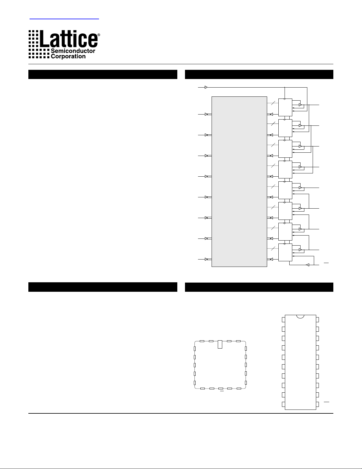
Functional Block Diagram
I/CLK
I
I
I
I
I
(64 X 32)
AND-ARRAY
I
I
I
PROGRAMMABLE
8
8
8
8
8
8
8
8
CLK
OLMC
OLMC
OLMC
OLMC
OLMC
OLMC
OLMC
OLMC
I/O/Q
I/O/Q
I/O/Q
I/O/Q
I/O/Q
I/O/Q
I/O/Q
I/O/Q
OE
I/OE
Description
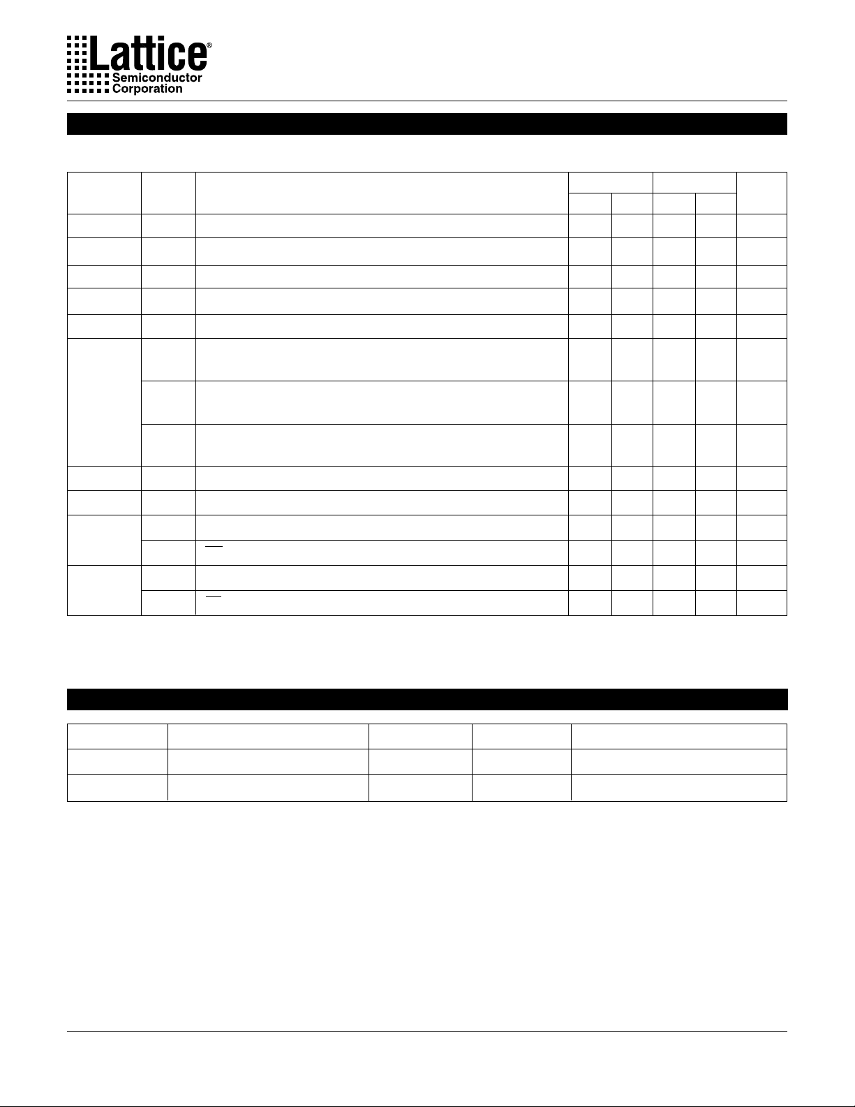
Pin Configuration
The GAL16V8/883 is a high performance E2CMOS programmable logic device processed in full compliance to MIL-STD-883.
This military grade device combines a high performance CMOS
process with Electrically Erasable (E
2
) floating gate technology to
LCC
CERDIP
provide the highest speed/power performance available in the
883 qualified PLD market. The GAL16V8D/883, at 7.5ns maximum propagation delay time, is the world's fastest military qualified CMOS PLD.
4
The generic GAL architecture provides maximum design flexibility by allowing the Output Logic Macrocell (OLMC) to be configured by the user. The GAL16V8/883 is capable of emulating all
standard 20-pin PAL
metric compatibility.
Unique test circuitry and reprogrammable cells allow complete
AC, DC, and functional testing during manufacture. Therefore,
Lattice Semiconductor delivers 100% field programmability and
functionality of all GAL products. In addition, 100 erase/write
cycles and data retention in excess of 20 years are specified.
Copyright © 1999 Lattice Semiconductor Corp. All brand or product names are trademarks or registered trademarks of their respective holders. The specifications and information herein are subject
to change without notice.
LATTICE SEMICONDUCTOR CORP., 5555 Northeast Moore Ct., Hillsboro, Oregon 97124, U.S.A. February 1999
Tel. (503) 268-8000; 1-800-LATTICE; FAX (503) 268-8556; http://www.latticesemi.com
16v8mil_03
®
devices with full function/fuse map/para-
I
I
6
I
I
8
I
1
I/CLKII
Vcc
I/O/Q
220
3
GAL16V8
T op View
91113
I GND
I/OE
19
I/O/Q I/O/Q
18
I/O/Q
I/O/Q
16
I/O/Q
I/O/Q
I/O/Q
14
GAL
16V8

Specifications GAL16V8D-7/10/883
Absolute Maximum Ratings
(1)
Supply voltage VCC...................................... –0.5 to +7V
Input voltage applied .......................... –2.5 to V
+1.0V
CC
Off-state output voltage applied .........–2.5 to VCC +1.0V
Recommended Operating Conditions
Case T emperature (TC)..............................–55 to 125°C
Supply voltage (V
with Respect to Ground ..................... +4.50 to +5.50V
CC
)
Storage Temperature ................................–65 to 150°C
Case T emperature with
Power Applied........................................–55 to 125°C
1.Stresses above those listed under the “Absolute Maximum Ratings” may cause permanent damage to the device. These are
stress only ratings and functional operation of the device at these
or at any other conditions above those indicated in the operational
sections of this specification is not implied (while programming,
follow the programming specifications).
DC Electrical Characteristics
Over Recommended Operating Conditions (Unless Otherwise Specified)
SYMBOL PARAMETER CONDITION MIN. TYP.
3
MAX. UNITS
VIL Input Low Voltage Vss – 0.5 — 0.8 V
VIH Input High Voltage 2.0 — Vcc+1 V
1
IIL
Input or I/O Low Leakage Current 0V ≤ VIN ≤ VIL (MAX.) — — –100 µA
IIH Input or I/O High Leakage Current 3.5V ≤ VIN ≤ VCC ——10µA
VOL Output Low Voltage IOL = MAX. Vin = VIL or VIH — — 0.5 V
VOH Output High Voltage IOH = MAX. Vin = VIL or VIH 2.4 — — V
IOL Low Level Output Current — — 12 mA
IOH High Level Output Current — — –2 mA
2
IOS
Output Short Circuit Current VCC = 5V VOUT = 0.5V TA= 25°C –30 — –150 mA
ICC Operating Power VIL = 0.5V VIH = 3.0V L-7/-10 — 75 130 mA
Supply Current f
1) The leakage current is due to the internal pull-up on all pins. See Input Buffer section for more information.
2) One output at a time for a maximum duration of one second. Vout = 0.5V was selected to avoid test problems caused by tester
ground degradation. Characterized but not 100% tested.
3) Typical values are at Vcc = 5V and TA = 25 °C
toggle = 15MHz Outputs Open
2
AC Switching Characteristics
Specifications GAL16V8D-7/10/883
Over Recommended Operating Conditions
PARAMETER UNITS
TEST
COND
DESCRIPTION
1
.
-7
MIN. MAX.
-10
MIN. MAX.
tpd A Input or I/O to Combinational Output 1 7.5 2 10 ns
tco A Clock to Output Delay 1617ns
2
tcf
— Clock to Feedback Delay — 6 — 7 ns
tsu — Setup Time, Input or Feedback before Clock↑ 7—10—ns
th — Hold Time, Input or Feedback after Clock↑ 0—0—ns
A Maximum Clock Frequency with 76.9 — 58.8 — MHz
External Feedback, 1/(tsu + tco)
3
fmax
A Maximum Clock Frequency with 76.9 — 58.8 — MHz
Internal Feedback, 1/(tsu + tcf)
A Maximum Clock Frequency with 100 — 62.5 — MHz
No Feedback
twh — Clock Pulse Duration, High 5 — 8 — ns
twl — Clock Pulse Duration, Low 5 — 8 — ns
ten B Input or I/O to Output Enabled 1 9 — 10 ns
B OE to Output Enabled 1 7 — 10 ns
tdis C Input or I/O to Output Disabled 1 9 — 10 ns
C OE to Output Disabled 1 7 — 10 ns
1) Refer to Switching T est Conditions section.
2) Calculated from fmax with internal feedback. Refer to fmax Descriptions section.
3) Refer to fmax Descriptions section.
Capacitance (TA = 25°C, f = 1.0 MHz)
SYMBOL PARAMETER MAXIMUM* UNITS TEST CONDITIONS
C
I
C
I/O
*Characterized but not 100% tested.
Input Capacitance 10 pF VCC = 5.0V , VI = 2.0V
I/O Capacitance 10 pF VCC = 5.0V , V
= 2.0V
I/O
3
Specifications GAL16V8D/883
Absolute Maximum Ratings
Supply voltage VCC...................................... –0.5 to +7V
Input voltage applied .......................... –2.5 to V
Off-state output voltage applied .........–2.5 to VCC +1.0V
Storage Temperature ................................–65 to 150°C
Case T emperature with
Power Applied........................................–55 to 125°C
1.Stresses above those listed under the “Absolute Maximum Ratings” may cause permanent damage to the device. These are
stress only ratings and functional operation of the device at these
or at any other conditions above those indicated in the operational
sections of this specification is not implied (while programming,
follow the programming specifications).
(1)
+1.0V
CC
Recommended Operating Conditions
Case T emperature (TC)..............................–55 to 125°C
Supply voltage (V
with Respect to Ground ..................... +4.50 to +5.50V
CC
)
DC Electrical Characteristics
Over Recommended Operating Conditions (Unless Otherwise Specified)
SYMBOL PARAMETER CONDITION MIN. TYP.2MAX. UNITS
VIL Input Low Voltage Vss – 0.5 — 0.8 V
VIH Input High Voltage 2.0 — Vcc+1 V
IIL Input or I/O Low Leakage Current 0V ≤ VIN ≤ VIL (MAX.) — — –10 µA
IIH Input or I/O High Leakage Current 3.5V ≤ VIN ≤ VCC ——10µA
VOL Output Low Voltage IOL = MAX. Vin = VIL or VIH — — 0.5 V
VOH Output High Voltage IOH = MAX. Vin = VIL or VIH 2.4 — — V
IOL Low Level Output Current — — 12 mA
IOH High Level Output Current — — –2 mA
1
IOS
Output Short Circuit Current VCC = 5V VOUT = 0.5V TA= 25°C –30 — –150 mA
ICC Operating Power VIL = 0.5V VIH = 3.0V L -15/ -20/-30 — 75 130 mA
Supply Current f
1) One output at a time for a maximum duration of one second. Vout = 0.5V was selected to avoid test problems caused by tester
ground degradation. Characterized but not 100% tested.
3) T ypical values are at Vcc = 5V and TA = 25 °C
toggle = 15MHz Outputs Open
4

AC Switching Characteristics
Specifications GAL16V8D/883
Over Recommended Operating Conditions
PARAMETER UNITS
TEST
COND
DESCRIPTION
1
.
-15
MIN. MAX.
-20
MIN. MAX.
-30
MIN. MAX.
tpd A Input or I/O to Combinational Output 3 15 3 20 3 30 ns
tco A Clock to Output Delay 2 12 2 15 2 20 ns
2
tcf
— Clock to Feedback Delay — 12 — 15 — 20 ns
tsu — Setup T ime, Input or Feedback before Clock↑ 12 — 15 — 25 — ns
th — Hold Time, Input or Feedback after Clock↑ 0— 0— 0 —ns
A Maximum Clock Frequency with 41.6 — 33.3 — 22.2 — MHz
External Feedback, 1/(tsu + tco)
3
fmax
A Maximum Clock Frequency with 41.6 — 33.3 — 22.2 — MHz
Internal Feedback, 1/(tsu + tcf)
A Maximum Clock Frequency with 50 — 41.6 — 33.3 — MHz
No Feedback
twh — Clock Pulse Duration, High 10 — 12 — 15 — ns
twl — Clock Pulse Duration, Low 10 — 12 — 15 — ns
ten B Input or I/O to Output Enabled — 15 — 20 — 30 ns
B OE to Output Enabled — 15 — 18 — 25 ns
tdis C Input or I/O to Output Disabled — 15 — 20 — 30 ns
C OE to Output Disabled — 15 — 18 — 25 ns
1) Refer to Switching T est Conditions section.
2) Calculated from fmax with internal feedback. Refer to fmax Descriptions section.
3) Refer to fmax Descriptions section.
Capacitance (TA = 25°C, f = 1.0 MHz)
SYMBOL PARAMETER MAXIMUM* UNITS TEST CONDITIONS
C
I
C
I/O
*Characterized but not 100% tested.
Input Capacitance 10 pF VCC = 5.0V , VI = 2.0V
I/O Capacitance 10 pF VCC = 5.0V , V
= 2.0V
I/O
5
(
)
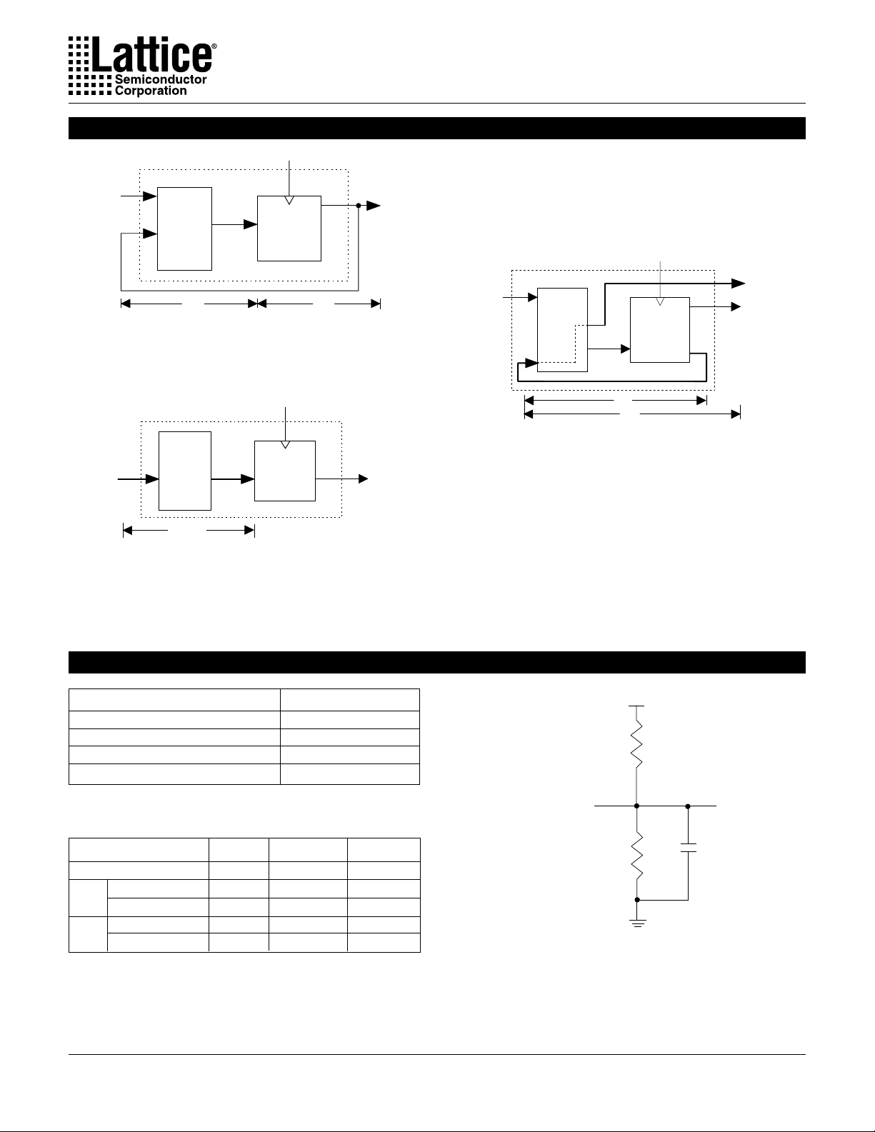
Switching Waveforms
Specifications GAL16V8/883
INPUT or
I/O FEEDBACK
COMBINATIONAL
OUTPUT
INPUT or
I/O FEEDBACK
COMBINATIONAL
OUTPUT
VALID INPUT
t
pd
INPUT or
I/O FEEDBACK
CLK
REGISTERED
OUTPUT
VALID INPUT
su
t
t
tco
1/
fmax
(external fdbk)
h
Registered OutputCombinatorial Output
OE
dis
t
en
t
REGISTERED
OUTPUT
dis
t
en
t
OE to Output Enable/DisableInput or I/O to Output Enable/Disable
CLK
wh
t
1/fmax
w/o fb
wl
t
CLK
REGISTERED
FEEDBACK
1/fmax (internal fdbk)
cf
t
su
t
Clock Width
fmax with Feedback
6
fmax Descriptions
Specifications GAL16V8/883
CLK
LOGIC
ARRAY
t
su
REGISTER
t
co
fmax with External Feedback 1/(tsu+tco)
Note: fmax with external feedback is calculated from measured
tsu and tco.
CLK
LOGIC
ARRAY
t
su + th
REGISTER
fmax with No Feedback
Note: fmax with no feedback may be less than 1/(twh + twl). This
is to allow for a clock duty cycle of other than 50%.
CLK
LOGIC
ARRAY
REGISTER
t
cf
t
pd
fmax with Internal Feedback 1/(tsu+tcf)
Note: tcf is a calculated value, derived by subtracting tsu from
the period of fmax w/internal feedback (tcf = 1/fmax - tsu). The
value of tcf is used primarily when calculating the delay from
clocking a register to a combinatorial output (through registered
feedback), as shown above. For example, the timing from clock
to a combinatorial output is equal to tcf + tpd.
Switching Test Conditions
Input Pulse Levels GND to 3.0V
Input Rise and Fall Times 3ns 10% – 90%
Input Timing Reference Levels 1.5V
Output Timing Reference Levels 1.5V
Output Load See Figure
3-state levels are measured 0.5V from steady-state active level.
Output Load Conditions (see figure)
T est Condition R
A 390Ω 750Ω 50pF
B Active High ∞ 750Ω 50pF
Active Low 390Ω 750Ω 50pF
C Active High ∞ 750Ω 5pF
Active Low 390Ω 750Ω 5pF
1 R2 CL
+5V
R
1
FROM OUTPUT (O/Q)
UNDER TEST
R
2
INCLUDES TEST FIXTURE AND PROBE CAPACITANCE
*C
L
C *
L
TEST POINT
7

Specifications GAL16V8/883
GAL16V8 Ordering Information (MIL-STD-883 and SMD)
dpT
)sn(
5.776031PIDRECniP-02388/DL7-D8V61LAGAR7093898-2695
01017 031PIDRECniP-02388/DL01-D8V61LAGAR4093898-2695
512121031PIDRECniP-02388/DL51-D8V61LAGAR3093898-2695
025151031PIDRECniP-02388/DL02-D8V61LAGAR2093898-2695
035202031PIDRECniP-02388/DL03-D8V61LAGAR1093898-2695
Note: Lattice Semiconductor recognizes the trend in military device procurement
towards using SMD compliant devices, as such, ordering by this number is recommended.
usT
)sn(
ocT
)sn(
ccI
)Am(
031CCLniP-02388/RL7-D8V61LAGA27093898-2695
031CCLniP-02388/RL01-D8V61LAGA24093898-2695
031CCLniP-02388/RL51-D8V61LAGA23093898-2695
031CCLniP-02388/RL02-D8V61LAGA22093898-2695
egakcaP388-DTS-LIM#DMS
#gniredrO
Part Number Description
GAL16V8D
Device Name
Speed (ns)
PowerL = Low Power
XXXXXXXX XX X X X
_
MIL Process /883 = 883 Process
Package
D = CERDIP
R = LCC
8
 Loading...