

Page 1

LatticeECP2/M sysCONFIG
Usage Guide
June 2013 Technical Note TN1108
Introduction
The configuration memory in the LatticeECP2™ and LatticeECP2M™ FPGAs is built using volatile SRAM; therefore, an external non-volatile configuration memory is required to maintain the configuration data when the power is
removed. This non-volatile memory supplies the configuration data to the LatticeECP2/M when it powers-up, or any
other time the device needs to be updated.
To support multiple configuration options the LatticeECP2/M supports the Lattice sysCONFIG™ interface, as well
as the dedicated ispJTAG™ port. The available configuration options, or ports, are listed in Table 15-1.
Table 15-1. Supported Configuration Ports
Interface Port
SPI
sysCONFIG
ispJTAG JTAG (IEEE 1149.1 and IEEE 1532 compliant)
SPIm
Slave Serial
Slave Parallel
This technical note covers all of the configuration options available for LatticeECP2/M.
General Configuration Flow
The LatticeECP2/M will enter configuration mode when one of three things happens, power is applied to the chip,
the PROGRAMN pin is driven low, or when a JTAG Refresh instruction is issued. Upon entering configuration mode
the INITN pin and the DONE pin are driven low to indicate that the device is initializing, i.e. getting ready to receive
configuration data.
Once the LatticeECP2/M has finished initializing, the INITN pin will be driven high. The low to high transition of the
INITN pin causes the CFG pins to be sampled, telling the LatticeECP2/M which port it is going to configure from.
The LatticeECP2/M then begins reading data from the selected port and starts looking for the preamble, BDB3
(hex). All data after the preamble is valid configuration data.
When the LatticeECP2/M has finished reading all of the configuration data, assuming there have been no errors,
the DONE pin goes high and the LatticeECP2/M enters user mode, in other words the device begins to function
according to the user’s design.
Note that the LatticeECP2/M may also be programmed via JTAG. When programming via JTAG, the INITN and
DONE signals have no meaning, because JTAG, per the IEEE standard, takes complete control of the chip and it’s
I/Os.
The Lattice ECP2/M devices are also available in an "S" version which supports the use of an encrypted bitstream
configuration file. These versions have the same configuration options as the standard versions, except where
noted in this document. When using these devices, the user should refer to the LatticeECP2/M Family Data Sheet
and TN1109, LatticeECP2/M Configuration Encryption Usage Guide, in addition to this document, to understand
the configuration requirements.
The following sections define each configuration pin, each configuration mode, and all of the configuration options
for the LatticeECP2/M.
© 2013 Lattice Semiconductor Corp. All Lattice trademarks, registered trademarks, patents, and disclaimers are as listed at www.latticesemi.com/legal. All other brand
or product names are trademarks or registered trademarks of their respective holders. The specifications and information herein are subject to change without notice.
www.latticesemi.com 15-1 tn1108_02.5
Page 2

LatticeECP2/M sysCONFIG Usage Guide
Configuration Pins
The LatticeECP2/M supports two types of configuration pins, dedicated and dual-purpose. The dedicated pins are
used exclusively for configuration; the dual-purpose pins, when not being used for configuration, are available as
extra I/O pins. If a dual-purpose pin is to be used both for configuration and as a general purpose I/O (GPIO) the
user must adhere to the following:
• The I/O type must remain the same, in other words if the pin is a 3.3V CMOS pin (LVCMOS33) during configuration it must remain a 3.3V CMOS pin as a GPIO.
• The user must select the correct CONFIG_MODE setting and set the PERSISTENT bit to OFF in order to use
the dual-purpose sysCONFIG pins as GPIO after configuration. In ispLEVER
®
these preferences can be set in
the Design Planner. If you are using Lattice Diamond™ design software, select Tools > Spreadsheet View and
then select the Global Preferences tab in the Spreadsheet View.
• The user is responsible for insuring that no internal or external logic will interfere with device configuration.
Also, if slave parallel configuration mode is not being used then one or both of the parallel port chip selects (CSN,
CS1N) must be high or tri-state during configuration.
Programmable options control the direction and type of each dual-purpose configuration pin. These options are
controlled via pin preferences in Lattice ispLEVER and Diamond software, or as HDL source file attributes.
The LatticeECP2/M also supports ispJTAG for configuration, transparent read back, and JTAG testing. The following sections describe the function of the various sysCONFIG and JTAG pins. Table 15-2 is provided for reference.
Table 15-2. Configuration Pins for the LatticeECP2/M
Pin Name I/O Type Pin Type Mode Used
CFG[2:0] Input, weak pull-up Dedicated All
PROGRAMN Input, weak pull-up Dedicated All
INITN Bi-Directional Open Drain, weak pull-up Dedicated All
DONE
CCLK Input or Output Dedicated All
DI/CSSPI0N
DOUT/CSON
2
CSN
CS1N
WRITEN
BUSY/SISPI
D[0]/SPIFASTN
D[1:6]
D[7]/SPID0
2
2
2
2
2
2
2
2
TDI Input, weak pull-up Dedicated JTAG
TDO Output, weak pull-up Dedicated JTAG
TCK Input with Hysteresis Dedicated JTAG
TMS Input, weak pull-up Dedicated JTAG
1. Weak pull-ups consist of a current source of 30µA to 150µA. The pull-ups for sysCONFIG dedicated and dual-purpose pins track V
the pull-ups for TDI, TDO, and TMS track V
2. The sysCONFIG pins on the LatticeECP2M50/M70/M100 are dedicated sysCONFIG pins. The sysCONFIG output pins are actively driven
during normal device operation.
Bi-Directional Open Drain with weak pullup, or Active Drive
Dedicated All
Input, weak pull up Dual-Purpose Serial, SPI, SPIm
Output Dual-Purpose Parallel, Serial, SPI
Input, weak pull-up Dual-Purpose Parallel
Input, weak pull-up Dual-Purpose Parallel
Input, weak pull-up Dual-Purpose Parallel
Output, tri-state, weak pull-up Dual-Purpose Serial, SPI, SPIm
Parallel, SPI, SPIm
Input or Output Dual-Purpose
Parallel
Parallel, SPI, SPIm
.
CCJ
CCIO8
;
15-2
Page 3

LatticeECP2/M sysCONFIG Usage Guide
Dedicated Control Pins
The following sub-sections describe the LatticeECP2/M dedicated sysCONFIG pins. These pins are powered by
V
While the device is under IEEE 1149.1 or 1532 JTAG control the dedicated programming pins have no meaning.
This is because a boundary scan cell will control each pin, per JTAG 1149.1, rather than normal internal logic.
CFG[2:0]
The Configuration Mode pins, CFG[2:0], are dedicated inputs with weak pull-ups. The CFG pins are sampled on
the rising edge of INITN and are used to select the configuration mode, i.e. what type of device the LatticeECP2/M
will configure from. As a consequence the CFG pins determine which groups of dual-purpose pins will be used for
device configuration (see the right-most column in Table 15-2). See Table 15-3 for a list of Configuration Modes.
Table 15-3. Configuration Modes
.
CCIO8
Configuration Mode CFG[2] CFG[1] CFG[0] D[0]/SPIFASTN
SPI
Reserved 001X
SPIm
Reserved 011X
Reserved 100X
Slave Serial 1 0 1 X
Reserved 110X
Slave Parallel 1 1 1 D0
Notes:
JTAG is always available for IEEE 1149.1 and 1532 support.
Normal (0x03) 0 0 0 Pull-Up
Fast (0x0B) 0 0 0 Pull-Down
Normal (0x03) 0 1 0 Pull-Up
Fast (0x0B) 0 1 0 Pull-Down
PROGRAMN
The PROGRAMN pin is a dedicated input with a weak pull-up. This pin is used to initiate a non-JTAG SRAM configuration sequence.
A high to low signal applied to PROGRAMN takes the device out of user mode and sets it into configuration mode.
The low to high transition will initiate the configuration process. The PROGRAMN pin can be used to trigger configuration at any time.
INITN
The INITN pin is a bidirectional open drain control pin. INITN is capable of driving a low pulse out as well as detecting a low pulse driven in.
When the PROGRAMN pin is driven low, or a JTAG Reset instruction is received, or after the internal Power-OnReset signal is released during power-up, the INITN pin will be driven low to reset the internal configuration circuitry. Once the PROGRAMN pin is driven high, the configuration initialization begins. Once the configuration initialization is completed, the INITN pin will go high. To delay configuration the INITN pin can be held low externally.
The device will not enter configuration mode as long as the INITN pin is held low. A low to high transition on INITN
causes the CFG pins to be sampled, telling the LatticeECP2/M which port to use, and starts configuration.
During configuration the INITN pin becomes an error detection pin. If a CRC error is detected during configuration
INITN will be driven low. The error will be cleared at the beginning of the next configuration.
15-3
Page 4

LatticeECP2/M sysCONFIG Usage Guide
DONE
The DONE pin is a dedicated bi-directional open drain with a weak pull-up (default), or it is an actively driven pin.
DONE goes low when INITN goes low, when INITN and PROGRAMN go high, and the internal Done bit is programmed at the end of configuration, the DONE pin will be released (or driven high, if it is an actively driven pin).
The DONE pin can be held low externally and, depending on the wake-up sequence selected, the device will not
become functional until the DONE pin is externally brought high. Externally delaying the wake-up sequence using
the DONE pin is a good way to synchronize the wake-up of multiple FPGAs; it is also required when configuring
multiple FPGAs from a single configuration device.
Sampling the DONE pin is a good way for an external device to tell if the FPGA has finished configuration. However, when using IEEE 1532 JTAG to configure SRAM the DONE pin is driven by a boundary scan cell, so the state
of the DONE pin has no meaning during IEEE 1532 JTAG configuration (once configuration is complete, DONE
reverts to internal logic and will be high).
CCLK
CCLK is a dedicated bi-directional pin; direction depends on whether a Master or Slave mode is selected. If a Master mode (SPI or SPIm) is selected, via the CFG pins, the CCLK pin becomes an output; otherwise CCLK is an
input.
If the CCLK pin becomes an output, the internal programmable oscillator is connected to CCLK and is driven out to
slave devices. CCLK will stop 120 clock cycles after the DONE pin is brought high. The extra clock cycles ensure
that enough clocks are provided to wake-up other devices in the chain. When stopped, CCLK becomes an input
(tri-stated output). CCLK will restart (become an output again) on the next configuration initialization sequence.
The MCCLK_FREQ parameter (one of the global preferences in the Design Planner of ispLEVER or the Spreadsheet View in Diamond) controls the CCLK master frequency (see data sheet On-Chip Oscillator section for the frequency selection). The software default setting for the configuration CCLK is 2.5 MHz. For a complete list of the
supported Master Clock frequencies, please see the LatticeECP2/M Family Data Sheet
during configuration is the MCCLK_FREQ parameter; once this parameter is loaded the frequency changes to the
selected value. Care should be exercised not to exceed the frequency specification of the slave devices or the signal integrity capabilities of the PCB layout.
When downloading an encrypted bitstream file to the LatticeECP2/M S-Series devices, the user must adhere to the
appropriate conditions for the CCLK signal. These conditions are shown in TN1109, LatticeECP2/M Configuration
Encryption Usage Guide.
. One of the first operations
Dual-Purpose sysCONFIG Pins
The following is a list of the dual-purpose sysCONFIG pins. If any of these pins are used for configuration and for
user I/O, the user must adhere to the requirements listed at the start of the Configuration pin sections. On
LatticeECP2M50/M70/M100 devices, the sysCONFIG pins described below are dedicated pins. When using the
same pins to access the external boot Flash, the system design must take care of tri-stating these output pins while
driving these pins from a different I/O pin.
These pins are powered by V
DI/CSSPI0N
The DI/CSSPI0N dual-purpose pin is designated as DI (Data Input) for Serial configurations. DI has an internal
weak pull-up. DI captures data on the rising edge of CCLK.
CCIO8
.
In SPI or SPIm mode the DI/CSSPI0N becomes a low true Chip Select output that drives the SPI Serial Flash chip
select.
DOUT/CSON
The DOUT/CSON pin is an output pin and has two purposes.
15-4
Page 5

LatticeECP2/M sysCONFIG Usage Guide
For serial and parallel configuration modes, when BYPASS mode is selected, this pin becomes DOUT (see
Figure 15-9). When the device is fully configured a Bypass instruction in the bitstream is executed and the data on
DI, or D[0:7] in the case of a parallel configuration mode, will then be routed to the DOUT pin. This allows data to
be passed, serially, to the next device. In a parallel configuration mode D0 will be shifted out first followed by D1,
D2, and so on.
For parallel configuration mode there is a Flowthrough option as well. When Flowthrough mode is selected this pin
becomes Chip Select Out (CSON). When the device is fully configured, and the Flowthrough instruction in the bitstream is executed, the CSON pin is driven low to enable the next device. The data pins, D[0:7], are wired in parallel to each device in the chain (see Figure 15-10).
In SPIm mode, the sysCONFIG daisy chaining mode of configuration is not supported.
The DOUT/CSON drives out a high on power-up and will continue to do so until the execution of the Bypass/Flow
Through instruction within the bitstream, or until the I/O Type is changed by the user code.
CSN and CS1N
Both CSN and CS1N are active low input pins with weak pull-ups and are used in parallel mode only. These inputs
are OR’ed and used to enable the D[0:7] data pins to receive or output a byte of data. Note: In the 144-pin TQFP
and 208-pin PQFP packages, CSN, CS1N and WRITEN are not bonded out.
When CSN or CS1N is high, the D[0:7], and BUSY pins are tri-stated. CSN and CS1N are interchangeable when
controlling the D[0:7], and BUSY pins. Driving both CSN and CS1N high causes the LatticeECP2/M to exit Bypass
or Flowthrough mode and resets the Bypass register. If Bypass or Flowthrough mode will not be used then CSN or
CS1N may be tied low, i.e. in this case it is only required that one of these pins be driven. The CSN and CS1N pins
must remain low while the configuration bitstream is being sent to the device or the configuration will fail.
If SRAM (configuration memory) needs to be accessed using the parallel pins while the part is in user mode (the
DONE pin is high) then the PERSISTENT preference must be set to ON to preserve these pins as CSN and CS1N.
CSN and CS1N are not connected in the 100-pin TQFP and 208-pin PQFP devices. Note that SRAM may only be
read using JTAG or Slave Parallel mode.
WRITEN
The WRITEN pin is an active low input with a weak pull-up and used for parallel mode only. Note: In the 144-pin
TQFP and 208-pin PQFP packages, CSN, CS1N and WRITEN are not bonded out.
The WRITEN pin is used to determine the direction of the data pins D[0:7]. The WRITEN pin must be driven low in
order to clock a byte of data into the device and driven high to clock data out of the device.
If SRAM (configuration memory) needs to be accessed using the parallel pins while the part is in user mode (the
DONE pin is high) then the PERSISTENT preference must be set to ON to preserve this pin as WRITEN. WRITEN
is not connected in the 100-pin TQFP and 208-pin PQFP devices. Note that SRAM may only be read using JTAG or
Slave Parallel mode.
BUSY/SISPI
The BUSY/SISPI pin has two functions.
In parallel configuration mode, the BUSY pin is a tri-stated output. The BUSY pin will be driven low by the device
only when it is ready to receive a byte of data on D[0:7] or a byte of data is ready for reading. The BUSY pin allows
the LatticeECP2/M to pause transfers on the parallel port.
If SRAM (configuration memory) needs to be accessed using the parallel pins while the part is in user mode (the
DONE pin is high) then the PERSISTENT preference must be set to ON to preserve this pin as BUSY. Note that
SRAM may only be read using JTAG or Slave Parallel mode.
In SPI or SPIm configuration modes, the BUSY/SISPI pin becomes an output that drives control and data to the
SPI Serial Flash. Control and data are output on the falling edge of CCLK. If SPI memory needs to be accessed
15-5
Page 6

LatticeECP2/M sysCONFIG Usage Guide
using the SPI port while the part is in user mode (the DONE pin is high) then the PERSISTENT preference must be
set to ON to preserve this pin as SISPI.
15-6
Page 7

LatticeECP2/M sysCONFIG Usage Guide
D[0]/SPIFASTN
The D[0]/SPIFASTN pin has two functions.
In parallel mode this pin is D[0] and operates in the same way as D[1:6] below. Taken together D[0:7] form the parallel data bus, D[0] is the most significant bit in the byte. As with D[1:6], if SRAM (configuration memory) needs to
be accessed using the parallel pins while the part is in user mode (the DONE pin is high) then the PERSISTENT
preference must be set to ON to preserve this pin as D[0]. Note that SRAM may only be read using JTAG or Slave
Parallel mode.
In SPI or SPIm mode the D[0]/SPIFASTN pin becomes an input. SPIFASTN is sampled on the rising edge of
INITN. If SPIFASTN is high the LatticeECP2/M will use SPI Serial Flash read op-code 03 (hex). Read op-code 03
(hex) is the standard read command used by all “25” series SPI Serial Flash. If SPIFASTN is low the
LatticeECP2/M will use SPI Serial Flash fast read op-code 0B (hex). The fast read op-code 0B (hex) accommodates higher frequency read clocks, exact clock speeds can be found in the SPI Serial Flash manufacturer’s data
sheet.
If SPI memory needs to be accessed using the SPI port while the part is in user mode (the DONE pin is high) then
the PERSISTENT preference must be set to ON to preserve this pin as SPIFASTN.
When using the SPI or SPIM mode the SPIFASTN pin should either be tied high or low. It must not be left floating
or configuration problems will occur.
Not all SPI Serial Flash support the 0B (hex) fast read op-code, consult the manufacturer’s data sheet. Care must
also be taken not to exceed the signal integrity capabilities of the PCB layout.
D[1:6]
The D[1:6] pins support parallel mode only. The D[1:6] pins are tri-statable bi-directional I/O pins used for data write
and read. When the WRITEN signal is low, and the CSN and CS1N pins are low, the D[1:6] pins become data
inputs. When the WRITEN signal is driven high, and the CSN and CS1N pins are low, the D[1:6] pins become data
outputs. If either CSN or CS1N is high D[1:6] will be tri-state.
If SRAM (configuration memory) needs to be accessed using the parallel pins while the part is in user mode (the
DONE pin is high) then the PERSISTENT preference must be set to ON to preserve this pin as D[1:6]. Note that
SRAM may only be read using JTAG or Slave Parallel mode.
Care must be exercised during read back of EBR or PFU memory. It is up to the user to ensure that reading these
RAMs will not cause data corruption; corruption may be caused when these RAMs are read while being accessed
by user code.
D[7]/SPID0
The D[7]/SPID0 pin has two functions.
In parallel mode this pin is D[7] and operates in the same way as D[1:6] above. Taken together D[0:7] form the parallel data bus, D[7] is the least significant bit in the byte. As with D[1:6], if SRAM (configuration memory) needs to
be accessed using the parallel pins while the part is in user mode (the DONE pin is high) then the PERSISTENT
preference must be set to ON to preserve this pin as D[7]. Note that SRAM may only be read using JTAG or Slave
Parallel mode.
In SPI or SPIm mode the D[7]/SPID0 pin becomes an input and should be wired to the output data pin of the SPI
Serial Flash. The data on SPID0 is clocked in on the rising edge of CCLK. If SPI memory needs to be accessed
using the SPI port while the part is in user mode (the DONE pin is high) then the PERSISTENT preference must be
set to ON to preserve this pin as SPID0.
ispJTAG Pins
The ispJTAG pins are standard IEEE 1149.1 TAP (Test Access Port) pins. The ispJTAG pins are dedicated pins and
are always accessible when the LatticeECP2/M device is powered up. While the device is under 1149.1 or 1532
15-7
Page 8

LatticeECP2/M sysCONFIG Usage Guide
JTAG control the dedicated programming pins INITN, DONE, and CCLK have no meaning. This is because a
boundary scan cell will control each pin, per the IEEE standard, rather than normal internal logic. While the
LatticeECP2/M is under JTAG control the PROGRAMN pin will be ignored.
These pins are powered by V
CCJ
.
TDO
The Test Data Output pin is used to shift out serial test instructions and data. When TDO is not being driven by the
internal circuitry, the pin will be in a high impedance state. This pin should be wired to TDO of the JTAG connector,
or to TDI of a downstream device in a JTAG chain. An internal pull-up resistor on the TDO pin is provided. The
internal resistor is pulled up to V
CCJ
.
TDI
The Test Data Input pin is used to shift in serial test instructions and data. This pin should be wired to TDI of the
JTAG connector, or to TDO of an upstream device in a JTAG chain. An internal pull-up resistor on the TDI pin is
provided. The internal resistor is pulled up to V
CCJ
.
TMS
The Test Mode Select pin controls test operations on the TAP controller. On the falling edge of TCK, depending on
the state of TMS, a transition will be made in the TAP controller state machine. An internal pull-up resistor on the
TMS pin is provided. The internal resistor is pulled up to V
CCJ
.
TCK
The test clock pin, TCK, provides the clock to run the TAP controller state machine, which loads and unloads the
JTAG data and instruction registers. TCK can be stopped in either the high or low state and can be clocked at frequencies up to that indicated in the device data sheet. The TCK pin supports hysteresis; the typical hysteresis is
approximately 100mV when V
and ground on the PCB of 4.7 K is recommended to avoid inadvertent clocking of the TAP controller as V
= 3.3V. The TCK pin does not have a pull-up. A pull-down resistor between TCK
CCJ
CC
ramps
up.
When downloading an encrypted bitstream file to the LatticeECP2/M S-Series devices, the user must adhere to the
appropriate conditions for the TCK signal. These conditions are shown in TN1109, LatticeECP2/M Configuration
Encryption Usage Guide.
Optional TRST
Test Reset, TRST, in not supported on the LatticeECP2/M.
V
CCJ
Having a separate JTAG VCC (V
) pin lets the user apply a voltage level to the JTAG port that is independent
CCJ
from the rest of the device. Valid voltage levels are 3.3V, 2.5V, 1.8V, 1.5V, and 1.2V, but the voltage used must
match the other voltages in the JTAG chain. V
Please see In-System Programming Design Guidelines for ispJTAG Devices
must be connected even if JTAG is not used.
CCJ
for further information.
Configuration and JTAG Pin Physical Description
All of the sysCONFIG dedicated and dual-purpose pins are part of Bank 8. Bank 8 V
determines the output
CCIO
voltage level of these pins, input thresholds are determined by the I/O Type selected in the ispLEVER Design Planner (default is 3.3V LVCMOS) or Diamond Spreadsheet View.
JTAG voltage levels and thresholds are determined by the V
pin, allowing the LatticeECP2/M to accommodate
CCJ
JTAG chain voltages from 1.2V to 3.3V.
Configuration Modes
The LatticeECP2/M devices support many different configuration modes, utilizing either serial or parallel data
paths. On power-up, when a JTAG Refresh instruction is issued, or when the PROGRAMN pin is toggled, the
CFG[2:0] pins are sampled to determine the configuration mode. See Table 15-3 above for a list of available configuration modes.
15-8
Page 9

LatticeECP2/M sysCONFIG Usage Guide
The following sub-sections break down each configuration mode. For more information on the options for each
mode, see the section below entitled Configuration Options.
SPI Mode
The LatticeECP2/M offers a direct connection to memories that support the SPI Serial Flash standard (see
Table 15-6). By setting the configuration pins, CFG[2:0], to all zeros the LatticeECP2/M will configure from the SPI
interface. The SPI interface supports two configuration topologies:
• One FPGA configured from one SPI Serial Flash
• Multiple FPGAs configured from one SPI Serial Flash
The required boot memory size for each of the ECP2/M device sizes is shown in Table 15-4. The values shown are
for a single LatticeECP2/M device. The size for a dual-boot application would be twice that shown.
Table 15-4. Maximum Configuration Bits - SPI Flash Mode Bitstream File
Device Bitstream Size (Mb) SPI Flash (Mb) Dual Boot SPI Flash (Mb)
ECP2-6 1.5 2 4 / 8
ECP2-12 2.9 4 8
ECP2-20 4.5 8 16
ECP2-35 6.3 8 16
ECP2-50 8.9 16 32
ECP2-70 13.3 16 32
ECP2M-20 5.9 8 16
ECP2M-35 9.8 16 32
ECP2M-50 15.8 16 64
ECP2M-70 19.8 32 64
ECP2M-100 25.6 32 64
1. These values apply for both encrypted and unencrypted bitstream files in the SPI Flash mode except as noted
below.
2. For the LatticeECP2-6 S-Series device, the dual Boot Flash size required is 8 Mb due to the number of sectors
required.
2
Table 15-5. Maximum Configuration Bits - Serial and Parallel Mode Bitstream File
All Modes Slave Serial Mode Slave Parallel Mode
Unencrypted Bitstream
Device
ECP2-6 1.5 2.3 7.5
ECP2-12 2.9 4.3 14.2
ECP2-20 4.5 6.7 22.0
ECP2-35 6.3 9.4 31.2
ECP2-50 8.9 13.4 44.3
ECP2-70 13.3 20.0 66.1
ECP2M-20 5.9 8.9 29.5
ECP2M-35 9.8 14.8 48.9
ECP2M-50 15.8 23.7 78.6
ECP2M-70 19.8 29.7 98.6
ECP2M-100 25.6 38.5 127.6
Size (Mb)
Encrypted Bitstream
Size (Mb)
Encrypted Bitstream
15-9
Size (Mb)
Page 10
LatticeECP2/M sysCONFIG Usage Guide
Lattice FPGA
SPI Mode
CCLK
DI/CSSPI0N
BUSY/SISPI
D7/SPID0 DOUT
CFG1
CFG0
SPIFASTN
SPI Serial
Flash
Q
C
CFG2
D0/SPIFASTN
PROGRAMN
DONE
D
/CS
The estimated time for configuration can be calculated by dividing the bitstream size (in bits) from Table 15-4 by the
CCLK frequency. The CCLK frequency can be set using the global preferences tab within the ispLEVER Design
Planner or the Spreadsheet View (Global Preferences tab) in Diamond. For more information on setting the CCLK
frequency, please see the Master Clock section and the D[0]/SPIFASTN pin section of this document.
When downloading an encrypted bitstream file to the LatticeECP2/M S-Series devices, the user must adhere to the
appropriate conditions for the CCLK signal. These conditions are shown in TN1109, LatticeECP2/M Configuration
Encryption Usage Guide.
Table 15-6. SPI Serial Flash Vendor List
Vendor Part Number
ST Microelectronics M25Pxx
Winbond W25Pxx
Silicon Storage Technology SST25VFxx,
SST25LFxx
Spansion S25FLxx
Atmel AT25Fxx
NexFlash NX25Pxx
Macronix MX25Lxx
Note: This is not meant to be an exhaustive list and may be updated
from time to time.
One FPGA, One SPI Flash
The simplest SPI configuration consists of one SPI Serial Flash connected to one LatticeECP2/M, as shown in
Figure 15-1. This is also the recommended method for use when downloading an encrypted bitstream file to the
LatticeECP2/M S-Series devices.
Figure 15-1. One FPGA, One SPI Serial Flash
Multiple FPGA, One SPI Flash
With a sufficiently large SPI Flash multiple FPGAs can be configured as shown in Figure 15-2. The first FPGA is
configured in SPI mode; the following FPGAs are configured in Slave Serial mode.
15-10
Page 11

Figure 15-2. Multiple FPGAs, One SPI Serial Flash
LatticeECP2/M sysCONFIG Usage Guide
SPI Serial
Flash
C
Q
D
/CS
SPIFASTN
PROGRAMN
DONE
Note: This method is not available when using encrypted bitstream files with the LatticeECP2/M S-Series devices.
Please refer to the LatticeECP2/M S-Series Configuration Encryption Usage Guide, TN1109, for more information
about using encrypted bitstream files.
Lattice FPGA
SPI Mode
CCLK
D7/SPID0 DOUT
BUSY/SISPI
DI/CSSPI0N
CFG2
CFG1
D0/SPIFASTN
CFG0
Lattice FPGA
Slave Serial
CCLK
DI/CSSPI0N
DOUT
CFG2
CFG1
CFG0
SPIm Mode
Externally, except for the CFG pins, SPIm mode looks like SPI mode, they use the same SPI Serial Flash devices,
and are wired to the FPGA in the same way (see Figure 15-6). The SPIm mode does not support multiple FPGAs
being configured from one SPI serial Flash as shown in Figure 15-2. Internally the two modes are treated differently.
SPI mode treats the SPI Serial Flash as a single block of storage starting at address zero. The SPIm mode treats
the SPI flash memory as discrete blocks of memory rather than a single block of memory. This allows the storage
of separate configuration images in separate blocks of memory. SPIm supports dual configuration (or boot) images,
here referred to as a “golden” image and a primary image.
A golden image is used when there is the possibility that corrupt data could be inadvertently loaded into the SPI
Serial Flash, such as during remote updates. For instance, if the Flash erase or program procedure is interrupted,
perhaps due to a power failure, then the Flash will contain corrupt data and the system could be rendered inoperable. Ideally the FPGA should detect that the data is corrupt and boot from a known good, or golden, boot image.
This is exactly what SPIm does.
The golden image is stored at the beginning of the Flash address space; the updatable, or primary, image is above
the golden image. During configuration, if the FPGA detects data corruption in the primary image, it will automatically reboot from the golden image. Each time the FPGA powers up, the PROGRAMN pin is toggled, or a JTAG
Refresh instruction is issued, it will try to configure from the primary image first. Note that if the LatticeECP2/M
detects that the data in the golden image is corrupt as well INITN will be driven low and the part will stop trying to
configure.
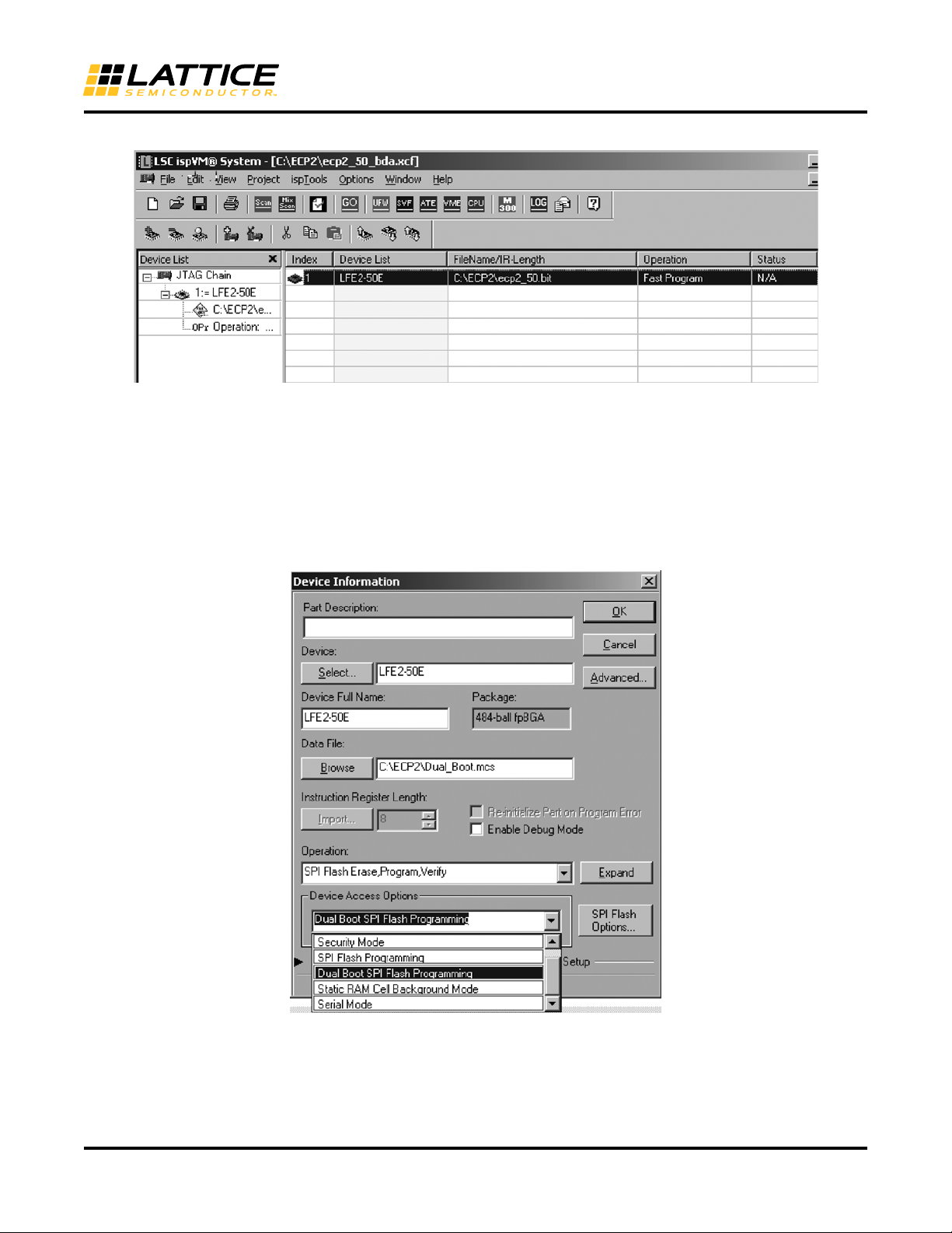
Dual Boot Image Setup
In order to use dual configuration files the files must first be properly stored within the SPI Serial Flash. Lattice
ispVM™ System software makes this easy.
15-11
Page 12
LatticeECP2/M sysCONFIG Usage Guide
Figure 15-3. ispVM Main Window
First, create the desired files using ispLEVER or Diamond. Depending on the application, these files might be the
same design or different designs. There is nothing special about these files, in other words they contain all of the
information needed to fully configure the FPGA.
Next, open ispVM (see Figure 15-3), do a scan of the board by clicking on the SCAN button on the toolbar, and
then double click on the row in the chain that has the LatticeECP2/M. You will now see the Device Information window (see Figure 15-4).
Figure 15-4. Device Information Window
From the Device Options drop-down box select Dual Boot SPI Flash Programming. Then click on the SPI Flash
Options button to open the SPI Serial Flash Device window (see Figure 15-5). In this window click on Select and
choose the SPI Flash that’s mounted on the board.
15-12
Page 13
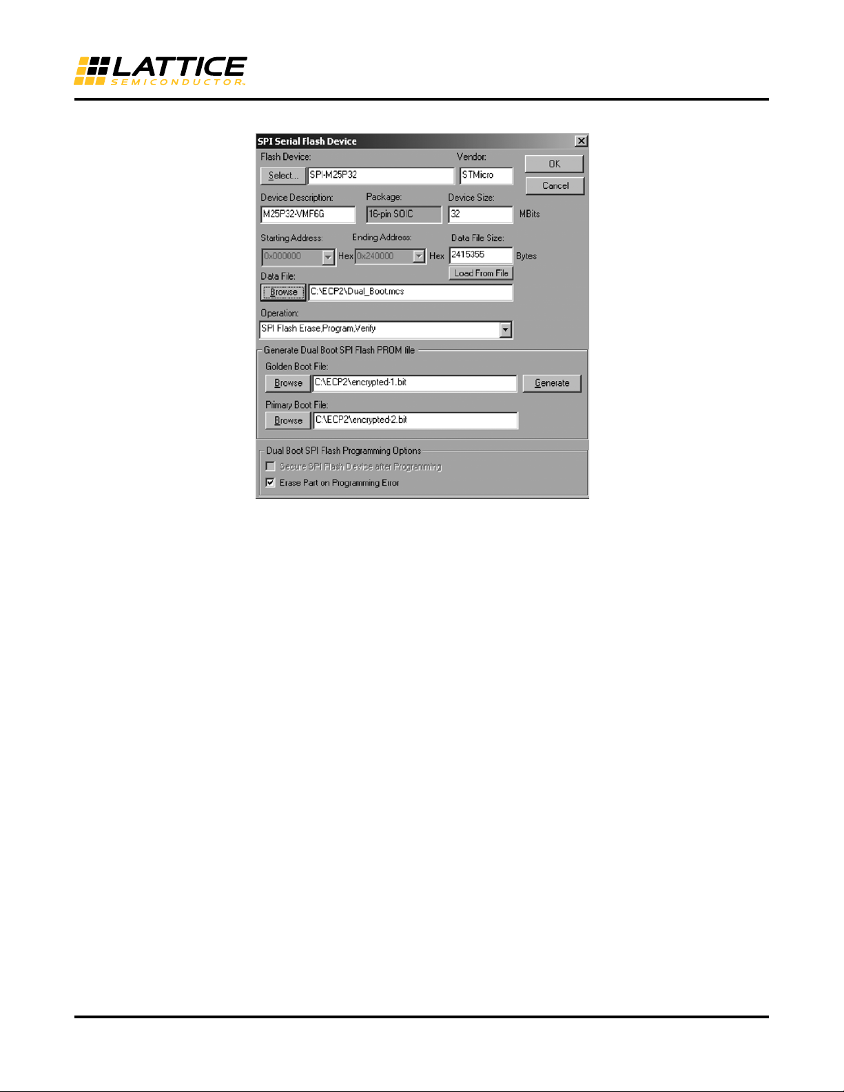
Figure 15-5. SPI Serial Flash Device Window
LatticeECP2/M sysCONFIG Usage Guide
Second, click on Browse to select an output file name.
Third, select an operation such as SPI Flash Erase, Program, Verify.
Fourth, select the golden file and primary file. Note that these may not be encrypted for the LatticeECP2/M “S” version.
And finally, click on the Generate button. When file generation is complete, click on OK to get back to the main
ispVM window. To program the file into the SPI Serial Flash just click on the GO button on the toolbar.
At power-up, when the PROGRAMN pin is toggled, or when a JTAG Refresh instruction is issued, the
LatticeECP2/M reads the primary file from SPI Serial Flash. If a CRC error is found then the LatticeECP2/M will reboot automatically, reading configuration data from the golden file instead of the primary file. Note that if an error is
found in the golden file the LatticeECP2/M will drive the INITN pin low and stop trying to configure.
Note that the flow specified here is for initial programming of the SPI Serial Flash. During a field update of the SPI
Serial Flash it is expected that only the primary configuration file will be updated, not the golden file. This is important because it guarantees the availability of a known good configuration file.
15-13
Page 14

LatticeECP2/M sysCONFIG Usage Guide
Lattice FPGA
SPIm Mode
CCLK
DI/CSSPI0N
BUSY/SISPI
D7/SPID0
CFG1
CFG0
SPIFASTN
CFG2
D0/SPIFASTN
PROGRAMN
DONE
SPI Serial Flash
Primary Boot
Golden Boot
Note: The CSSPI1N pin should not be connected.
Figure 15-6. SPIm, Dual Configuration Images
Programming SPI Serial Flash
The LatticeECP2/M contains dedicated hardware that allows JTAG to access the SPI port, allowing ispVM, embedded hardware, or ATE equipment to program the Flash while it is on the board. In order to program SPI Serial Flash
using JTAG, the CFG pins must be set to SPI or SPIm (see Table 15-3). Please refer to the ispVM Help system for
more information.
Slave Serial Mode
In Slave Serial mode the CCLK pin becomes an input, receiving the clock from an external device. The
LatticeECP2/M accepts data on the DI pin on the rising edge of CCLK. Slave Serial only supports writes to the
FPGA, it does not support reading from the FPGA.
After the device is fully configured, if the Bypass option has been set, any additional data clocked into DI will be
presented to the next device via the DOUT pin, as shown in Figure 15-7.
15-14
Page 15
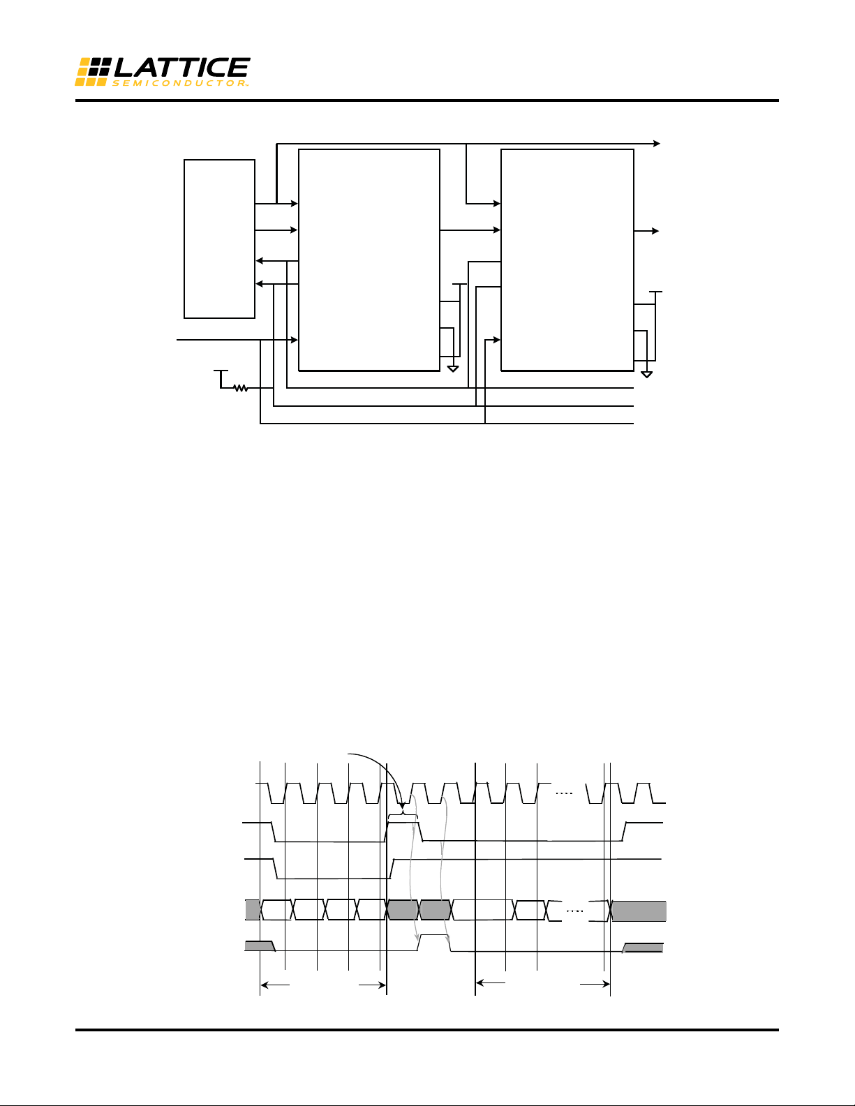
Figure 15-7. Serial Mode Daisy Chain
LatticeECP2/M sysCONFIG Usage Guide
Lattice FPGA
CPU
CLK
DATA
STATUS
STATUS
PROGRAM
Note: In the Slave Serial Mode, the Bypass option is not supported when using encrypted bitstream files with the
LatticeECP2/M S-Series devices. Please refer to the LatticeECP2/M S-Series Configuration Encryption Usage Guide,
TN1109, for more information about using encrypted bitstream files.
Slave Serial
CCLK
DI/CSSPI0N
DONE
INITN
PROGRAMN
DOUT
CFG2
CFG1
CFG0
Lattice FPGA
Slave Serial
CCLK
DI/CSSPI0N
DONE
INITN
PROGRAMN
DOUT
CFG2
CFG1
CFG0
Slave Parallel Mode
In Slave Parallel mode a host system sends the configuration data in a byte-wide stream to the LatticeECP2/M.
The CCLK, CSN, CS1N, and WRITEN pins are driven by the host system. WRITEN, CSN, and CS1N must be held
low to write to the device; data is input from D[0:7]. D0 is the MSb and D7 is the LSb.
Slave Parallel mode can also be used for readback of the internal configuration. By driving the WRITEN pin low,
and CSN and CS1N low, the device will input the readback instructions on the D[0:7] pins; WRITEN is then driven
high and read data is output on D[0:7] (see Figure 15-8). In order to support readback, the PERSISTENT bit must
be set to ON in ispLEVER Design Planner or in the Diamond Spreadsheet View (Global Preferences tab). Note:
SLAVE PARALLEL Mode is not available in the 100-pin TQFP and 208-pin PQFP package offerings since the
CSN, CS1N and WRITEN pins are not bonded out for these packages.
Figure 15-8. Parallel Port Read Timing Diagram
CSN pulse width is
dependent on the time
required to disable the
external D[0:7] driver.
CCLK
CSN
CS1N
WRITEN
D[0:7]
BUSY
Send Read
Command
Read Data
15-15
Page 16

LatticeECP2/M sysCONFIG Usage Guide
The host sends the preamble, BDB3 (hex), and then sends the read command. The LatticeECP2/M sends read
data on D[0:7], driving BUSY high as needed to pause data flow. For an example bitstream see Table 15-7.
Table 15-8 lists the various read commands. Note that the sample bitstream and the list of read commands are for
reference only; to help the user better understand the flow. The actual bitstream, containing the read commands, is
generated by ispLEVER or Diamond and ispVM, the host, toggles the control signals and sends the bitstream.
Table 15-7. Parallel Port Read Bitstream Example
Frame Contents Description
1111...1111 2 Dummy Bytes
Header
Verify ID 8 bytes of command and data
Reset Address 4 bytes of command and data
Read Increment 4 bytes of command and data
Table 15-8. Parallel Port Read Commands
Command 32-bit Opcode Function
Reset Address E2000000 Reset address register to point to the first data frame
Read Increment 01vvvvvv
Read Usercode 83000000 Read the content of the USERCODE register
Read Ctrl Reg 0 84000000 Read the content of Control Register 0
Read CRC 86000000 Read CRC register content
Read ID Code 87000000 Read ID code
NO OP FF
Note: x = don't care, v = variable.
10111101
10110011
Read back the configuration memory frame selected by the address register and
post increment the address
No operation. This is an 8-bit Opcode. Extra bits should not be appended to this
Opcode as this could cause INITN to go low during configuration.
2-byte Preamble (BDB3)
Slave Parallel mode can support two types of overflow, Bypass and Flowthrough. After the first device has received
all of it’s configuration data, and the Bypass command is detected in the bitstream, the data presented to the D[0:7]
pins will be serialized and bypassed to the DOUT pin (see Figure 15-9). If the Flowthrough command is detected in
the bitstream, instead of the bypass command, the CSON signal will drive the following parallel mode device’s chip
select low as shown in Figure 15-10. If either type of overflow is active, driving both the CSN and CS1N pins high
will reset overflow, i.e. take the device out of overflow.
15-16
Page 17

Figure 15-9. Slave Parallel with Bypass Option
Lattice FPGA
Slave Parallel
CCLK
D[0:7]
DONE
INITN
DOUT
CFG1
CFG0
CFG2
CS1N
PROGRAM
Lattice FPGA
Slave Serial
DOUT
CFG1
CFG0
CFG2
CCLK
DI/CSSPI0N
DONE
INITN
PROGRAMN
BUSY
WRITEN
CSN
PROGRAMN
WRITEN
BUSY
CLOCK
DATA
DONE
INIT
Select1
Select2
Note: In Slave Parallel mode, the Bypass option is not supported when using encr ypted bitstream files with the
LatticeECP2/M S-Series devices. Please refer to the LatticeECP2/M S-Series Configuration Encryption Usage Guide,
TN1109, for more information about using encrypted bitstream files.
LatticeECP2/M sysCONFIG Usage Guide
15-17
Page 18

Figure 15-10. Slave Parallel with Flowthrough
INITN
DONE
D[0:7]
CCLK
Lattice FPGA
Slave Parallel
LatticeECP2/M sysCONFIG Usage Guide
Lattice FPGA
Slave Parallel
CCLK
D[0:7]
DONE
INITN
BUSY
WRITEN
SELECTN
PROGRAM
BUSY
WRITEN
FT_RESET
Note: In Slave Parallel mode, the Flowthrough option is not supported when using encrypted bitstream files with the
LatticeECP2/M S-Series devices. Please refer to the LatticeECP2/M S-Series Configuration Encryption Usage Guide,
TN1109, for more information about using encrypted bitstream files.
CSN
CS1N
PROGRAMN
CSON
CFG2
CFG1
CFG0
CCLK
D[0:7]
DONE
INITN
BUSY
WRITEN
CSN
CS1N
PROGRAMN
CSON
CFG2
CFG1
CFG0
To support asynchronous configuration, where the host may provide data faster than the FPGA can accept it, Slave
Parallel mode can use the BUSY signal. By driving the BUSY signal high the Slave Parallel device tells the host to
pause sending data. Please note that all data and control are still synchronous with CCLK, asynchronous refers to
the ability to throttle the data transfer using BUSY. See Figure 15-11.
Figure 15-11. Parallel Port Write Timing Diagram
……
CCLK
…
PROGRAMN
INITN
CSN
CS1N
WRITEN
D[0:7]
Next Command
BUSY
Current Command
Note: When downloading an encrypted bitstream file to the LatticeECP2/M S-Series devices, the user must
adhere to the appropriate conditions for the CCLK signal. These conditions are shown in the LatticeECP2/M
S-Series Configuration Encryption Usage Guide, TN1109.
Write Write
Write
Write
The CSN and CS1N pins must remain low while the configuration bitstream is being sent to the device or the configuration will fail. To temporarily stop the write process, the user can pause the CCLK signal and the data. An
example of this is shown in Figure 15-11.
15-18
Page 19

LatticeECP2/M sysCONFIG Usage Guide
ispJTAG Mode
The LatticeECP2/M device can be configured through the ispJTAG port using either Fast Program or IEEE 1532
mode. The JTAG port is always on and available, regardless of the configuration mode selected. The IEEE 1532
mode is called Erase, Program, Verify in ispVM System.
Fast Program
Fast Program can be thought of as serial configuration using the JTAG port. The data file used for Fast Program is
the same as a file used for a sysCONFIG Serial mode configuration, in other words there is a header, a preamble,
and configuration data. Fast Program will result in a faster configuration time since the bitstream contains CRC
checking so a time consuming post programming bit by bit verification is not required. The SVF and VME file formats also support Fast programming.
During JTAG configuration the Boundary Scan cells take control of the LatticeECP2/M I/Os. The Boundary Scan
cells will usually drive the I/Os to a tri-state level but this can be controlled and even customized using ispVM. Note
that PROGRAMN, INITN, and DONE have no meaning since they are controlled by the Boundary Scan cells during
JTAG configuration. However, the INITN and DONE do indicate configuration status after JTAG configuration is
completed.
IEEE 1532
Besides Fast Program the LatticeECP2/M can also be configured through JTAG using the IEEE 1532 Standard.
The IEEE 1532 mode is called Erase, Program, Verify in ispVM System. IEEE 1532 configuration files contain
JTAG instructions, as well as the configuration data. IEEE 1532 files, including ISC, SVF, and VME, can be created
using ispVM’s Universal File Writer (UFW). These files can be used by ispVM or by third party ATE equipment.
These files can also be used in embedded situations, where an on-board processor provides the data while controlling the JTAG signals (this is called ispVM Embedded, more information can be found in ispVM’s help facility).
IEEE 1532 programming will be slower than the Fast Program mode since it requires a post programming bit by bit
verification.
During JTAG configuration the Boundary Scan cells take control of the LatticeECP2/M I/Os. The Boundary Scan
cells will usually drive the I/Os to a tri-state level but this can be controlled and even customized using ispVM.
Note that PROGRAMN, INITN, and DONE have no meaning since they are controlled by the Boundary Scan cells
during JTAG configuration. However, the DONE pin will indicate configuration status after IEEE 1532 configuration
is completed.
Transparent Read Back
The ispJTAG transparent read back mode allows the user to read the content of the device while the device
remains fully functional. All I/O, as well at the non-JTAG configuration pins, remain under internal logic control during a Transparent Read Back. The device enters the Transparent Read Back mode through a JTAG instruction. The
user must ensure that Transparent Read Back does not access EBR or distributed RAM at the same time internal
logic is accessing these resources or corruption of the RAM may occur.
Boundary Scan and BSDL Files
The LatticeECP2/M BSDL files can be found on the Lattice Semiconductor web site. The boundary scan ring covers all of the I/O pins, as well as the dedicated and dual-purpose sysCONFIG pins. Note that PROGRAMN, CCLK,
and the CFG pins are observe only (BC4, JTAG read-only) boundary scan cells.
Configuration Options
Several configuration options are available for each configuration mode.
• When daisy chaining multiple FPGA devices an overflow option is provided for serial and parallel configuration
modes
• When using SPI or SPIm mode, the master clock frequency can be set
• A security bit can be set to prevent SRAM readback
15-19
Page 20

LatticeECP2/M sysCONFIG Usage Guide
• The bitstream can be compressed
• The Persistent option can be set
• Configuration pins can be protected
• DONE pin options can be selected
By setting the proper parameter in the Lattice design software the selected configuration options are set in the generated bitstream. As the bitstream is loaded into the device the selected configuration options take effect. These
options are described in the following sections.
Bypass Option
In ispLEVER, the Bypass option can be set by using the Bitgen properties. Or, a chain of bitstreams can be assembled and Bypass set using ispVM. To set the Bypass option in Diamond, see Appendix A. The Bypass option can
be used in parallel and serial mode daisy chains. The Bypass option is not supported when using SPIm configuration. The Bypass option is not supported when using encrypted bitstream files with the LatticeECP2/M S-Series
devices. Please refer to TN1109, LatticeECP2/M Configuration Encryption Usage Guide
about using encrypted bitstream files.
When the first device completes configuration, and a Bypass command is input from the bitstream, any additional
data coming into the FPGA configuration port will overflow serially on DOUT. This data is applied to the DI pin of
the next device (downstream devices must be set to slave serial mode).
In serial configuration mode the Bypass option connects DI to DOUT via a bypass register. The bypass register is
initialized with a ‘1’ at the beginning of configuration and will stay at that value until the Bypass command is executed. In parallel configuration mode the Bypass option causes the excess data coming in on D[0:7] to be serially
shifted to DOUT. The serialized data is shifted to DOUT through a bypass register. D0 will be shifted out first followed by D1, D2, and so on. Once the Bypass option starts the device will remain in Bypass until the Wake-up
sequence completes. In parallel mode, if Bypass needs to be aborted, drive both CSN and CS1N high, this acts as
a Bypass reset signal.
, for more information
Flowthough Option
As with Bypass, Flowthrough can be set in the Bitgen properties in ispLEVER and in the Strategy Process Options
settings. To set the Flowthrough option in Diamond, see Appendix A. The Flowthrough option can be used with parallel daisy chains only. The Flowthrough option is not supported when using SPIm configuration. The Flowthrough
option not supported when using encrypted bitstream files with the LatticeECP2/M S-Series devices. Please refer
to TN1109, LatticeECP2/M Configuration Encryption Usage Guide
stream files.
When the first device completes configuration, and a Flowthrough command is input from the bitstream, the CSON
pin is driven low. In addition to driving CSON low, Flowthrough also tri-states the device’s D[0:7] and BUSY pins in
order to avoid contention with the other daisy-chained devices. Once the Flowthrough option starts the device will
remain in Flowthrough until the Wake-up sequence completes. If Flowthrough needs to be aborted drive both CSN
and CS1N high, this acts as a Flowthrough reset signal.
Master Clock
If the CFG pins indicate an SPI or SPIm mode the CCLK pin will become an output, with the frequency set by the
user. The default Master Clock Frequency is 3.1 MHz. For a complete list of the supported Master Clock frequencies, please see the LatticeECP2/M Family Data Sheet
available frequencies are restricted, as shown in the data sheet.
The user can change the Master Clock frequency by setting the MCCLK_FREQ global preference in the Lattice
ispLEVER Design Planner. To set this option in Diamond, see Appendix A. One of the first things loaded during
configuration is the MCCLK_FREQ parameter; once this parameter is loaded the frequency changes to the
selected value using a glitchless switch. Care should be exercised not to exceed the frequency specification of the
slave devices or the signal integrity capabilities of the PCB layout.
. When using the LatticeECP2/M S-Series devices, the
, for more information about using encrypted bit-
15-20
Page 21

LatticeECP2/M sysCONFIG Usage Guide
Configuration time is computed by dividing the maximum number of configuration bits, as given in Table 15-4
above, by the Master Clock frequency.
Security Bit
Setting the CONFIG_SECURE option to ON prevents readback of the SRAM from JTAG or the sysCONFIG pins.
When CONFIG_SECURE is set to ON the only operations available are erase and write. The security fuse is
updated as the last operation of SRAM configuration. If a secured device is read it will output all zeros.
For LatticeECP2/M devices the CONFIG_SECURE option is accessed via the Design Planner in ispLEVER. To set
this option in Diamond, see Appendix A. The default is OFF.
For the LatticeECP2/M S-Series devices (part numbers ECP2-XXES and ECP2MXXES) the CONFIG_SECURE
option is accessed using the Security Setting option under the Tools menu.
Compress Bitstream
Setting the global COMPRESS_CONFIG option to ON in ispLEVER Design Planner will cause the software to generate a compressed bitstream. To set this option in Diamond, see Appendix A. The LatticeECP2/M will automatically decompress the bitstream as it comes into the device. The actual amount of compression varies according to
the data pattern in the uncompressed bitstream. Though unlikely, it is theoretically possible for the compressed bitstream to be larger than the uncompressed bitstream.
Compressing the bitstream can result in faster configuration. The default setting is OFF.
Persistent Option
The PERSISTENT Option is set using ispLEVER Design Planner (default is OFF). To set this option in Diamond,
see Appendix A. PERSISTENT serves two purposes.
Setting PERSISTENT ON tells the place and route tools that it may not use any of the sysCONFIG pins associated
with the parallel port (all of the dual-purpose pins except DI) or the SPI Port pins.
Setting PERSISTENT ON also sets a hardware fuse. So, not only are the pins reserved in software, they are also
reserved in hardware.
PERSISTENT is set to ON when the user wants to be able to read the SRAM configuration memory using the
Slave Parallel port. In order to perform a read using the parallel port the user must first send a read command, setting PERSISTENT ON allows the parallel port to listen for this command while in user mode (the DONE pin is
high). If the design does not require this function, the PERSISTENT option should be set to OFF.
The PERSISTENT preference must also be set to ON if the SPI memory needs to be accessed using the SPI port
while the part is in user mode (the DONE pin is high) to preserve the SPI port pins.
Configuration Mode
Just as the CFG pins tell the hardware which port to configure from; the CONFIG_MODE option tells the software
which port will be used. CONFIG_MODE allows the user to protect dual-purpose sysCONFIG pins. For example
setting CONFIG_MODE to SPI will keep the Place and Route tools from using the SPI pins as general purpose I/O.
The user, however, is still free to assign these pins as GPIO, but a warning will be generated as a reminder that
there are certain precautions (see the section above entitled Configuration Pins).
Available options are NONE, JTAG, SPI, SPIm, Slave Serial, and Slave Parallel. The default is Slave Serial.
DONE_OD, DONE_EX
During configuration the DONE pin is low. Once configuration is complete, indicated by the setting of the internal
Done bit, the device wake-up sequence takes place and then the DONE pin goes high. Under most circumstances,
this flow is exactly what is needed, however, if there are several devices in one configuration chain, delay of the
wake-up sequence may be desirable in order to “synchronize” the wake-up of all devices in the chain. There are
two options that allow for this synchronization. These options are set in ispLEVER Design Planner. To set these
options in Diamond, see Appendix A.
15-21
Page 22

LatticeECP2/M sysCONFIG Usage Guide
DONE_OD defaults to ON. DONE_OD ON forces the DONE pin type to be open- drain. When connecting multiple
DONE pins together all of the pins should be open- drain, however it may be advantageous to have an actively
driven DONE pin on the last device. Setting DONE_OD to OFF makes the DONE pin an actively driven pin, rather
than open-drain.
DONE_EX defaults to OFF. Setting DONE_EX to ON will cause LatticeECP2/M to sample the DONE pin and, if the
DONE pin is held low externally, delay the wake-up sequence. Setting DONE_EX to OFF will cause the device to
wake-up as soon as the internal Done bit is set.
Device Wake-Up
When configuration is complete the device will wake up in a predictable fashion. Wake-Up occurs after successful
configuration, without errors, and provides the transition from Configuration Mode to User Mode. The Wake-Up process begins when the internal Done bit is set.
Table 15-9 provides a list of the Wake-Up sequences supported by the LatticeECP2/M; Figure 15-12 shows the
Wake-Up timing. The WAKE_UP defaults work fine for the vast majority of applications. To set the WAKE_UP
options in Diamond, see Appendix A.
Table 15-9. Wake-Up Options
Sequence Phase T0 Phase T1 Phase T2 Phase T3
1 DONE GOE, GWDIS, GSR
2 DONE GOE, GWDIS, GSR
3 DONE GOE, GWDIS, GSR
4 DONE GOE GWDIS, GSR
5 DONE GOE GWDIS, GSR
6 DONE GOE GWDIS GSR
7 DONE GOE GSR GWDIS
8 DONE GOE, GWDIS, GSR
9 DONE GOE, GWDIS, GSR
10 DONE GWDIS, GSR GOE
11 DONE GOE GWDIS, GSR
12 DONE GOE, GWDIS, GSR
13 GOE, GWDIS, GSR DONE
14 GOE DONE GWDIS, GSR
15 GOE, GWDIS DONE GSR
16 GWDIS DONE GOE, GSR
17 GWDIS, GSR DONE GOE
18 GOE, GSR DONE GWDIS
19 GOE, GWDIS, GSR DONE
20 GOE, GWDIS, GSR DONE
21 (Default) GOE GWDIS, GSR DONE
22 GOE, GWDIS GSR DONE
23 GWDIS GOE, GSR DONE
24 GWDIS, GSR GOE DONE
25 GOE, GSR GWDIS DONE
15-22
Page 23

LatticeECP2/M sysCONFIG Usage Guide
BCLK
DONE BIT
GLOBAL OUTPUT ENABLE
GLOBAL SET/RESET
GLOBAL WRITE DISABLE
DONE PIN
T0 T1 T2 T3
Figure 15-12. Wake-Up Timing Diagram
Synchronizing Wake-Up
The internal Wake-Up sequence clock source can be chosen as well as how the device wakes up relative to other
devices.
Wake-Up Clock Selection
The Wake-Up sequence is synchronized to a clock source that is user selectable. The clock sources are External
(default) and User Clock.
When External is selected the LatticeECP2/M will use one of two clocks during the Wake-Up sequence, depending
on the configuration data source. If the LatticeECP2/M is being configured from JTAG then JTAG’s TCK will be
used for the Wake-Up sequence, if configuration data is coming from a sysCONFIG port (serial, parallel, or SPI)
then CCLK will be used.
When User is selected, any of the clock signals in the design can be used as the clock source.
Synchronous to Internal Done Bit
If the LatticeECP2/M is the only device in the configuration chain, or the last device in the chain, DONE_EX should
be set to the default value (OFF). The Wake-Up process will be initiated by setting of the internal Done bit on successful completion of configuration.
Synchronous to External DONE Pin
The DONE pin can be used to synchronize Wake-Up to other devices in the configuration chain. If DONE_EX (see
the DONE_OD, DONE_EX section above) is ON then the DONE pin is a bi-directional pin. If an external device
drives the DONE pin low then the Wake-Up sequence will be delayed; configuration can complete but Wake-Up is
delayed. Once the DONE pin goes high the device will follow the selected WAKE_UP sequence.
In a configuration chain, a chain of devices configuring from one source (such as Figure 15-2), it is usually desirable, or even necessary, to delay wake-up of all of the devices until the last device finishes configuration. This is
accomplished by setting DONE_OD to OFF and DONE_EX to OFF on the last device while setting DONE_OD to
ON and DONE_EX to ON for the other devices.
Wake-Up Sequence Options
The Wake-Up sequence options shown in Table determine the order of application for three internal signals, GSR,
GWDIS, and GOE, and one external signal, DONE.
• GSR is used to set and reset the core of the device. GSR is asserted (low) during configuration and de-asserted
(high) in the Wake-Up sequence.
15-23
Page 24

LatticeECP2/M sysCONFIG Usage Guide
• When the GWDIS signal is low it safeguards the integrity of the RAM Blocks and LUTs in the device. This signal
is low before the device wakes up.
• When low, GOE prevents the device’s I/O buffers from driving the pins.
• When high, the DONE pin indicates that configuration is complete and that no errors were detected.
If DONE_EX (see DONE_OD, DONE_EX above) is OFF then sequence 21 is the default, but the user can select
any sequence from 8 to 25; if DONE_EX is ON the default sequence is 4, but the user can select any sequence
from 1 to 7.
Configuration FAQs
Here are some of the more common questions regarding device configuration.
General
• Q. Other than JTAG, what is the least expensive method of configuration?
A. If you already have a processor and extra storage on the board you can use the processor to feed configura-
tion data to the LatticeECP2/M. The least expensive stand-alone configuration option is SPI Serial Flash.
• Q. I have created my bitstream, now how do I load the bitstream into the LatticeECP2/M?
A. Use the free Lattice ispVM tool (from www.latticesemi.com
), and a Lattice ispDOWNLOAD® cable.
• Q. I can’t read the LatticeECP2/M device ID using JTAG. What could be wrong?
A. This is the most basic of JTAG operations. If you are having trouble reading the device ID then something
basic is wrong. Check that the JTAG connections are correct, and that V
rect (and the same). Make sure that the XRES pin is connected to ground through a 10K resistor. Check that all
LatticeECP2/M V
touching a properly grounded ‘scope probe to TCK will change the symptoms; if so, you have signal noise
issues. Check for excessive noise on the V
• Q. Is there anything I can do during board design that will make debugging easier?
A. Bring the dedicated configurations pins, PROGRAMN, INITN, DONE, and CCLK out to accessible test points.
• Q. Do I need external pull-up resistors on PROGRAMN, INITN, or DONE?
A. All of these signals have internal weak pull-ups, however if you have a noisy environment, or have several
devices connected to these pins, adding a 10K pull-up to the signal is recommended.
• Q. How can I get assistance with configuration issues?
A. Use the On-line Assistant feature in ispVM. You will find it under the Help menu.
and ground pins are properly connected. Check for noise on the JTAG signals. Sometimes
CC
pins.
CC
and the download cable VCC are cor-
CCJ
15-24
Page 25

LatticeECP2/M sysCONFIG Usage Guide
Mode Specific
SPI/SPIm
• Q. How do I program the SPI Serial Flash once it’s on the board?
A. Connect the SPI Serial Flash to the LatticeECP2/M as shown in this document, then use ispVM, and a Lattice
ispDOWNLOAD cable connected to the JTAG port, to program the bitstream into the Flash.
LatticeECP2/M devices have a JTAG instruction for programming the SPI Serial Flash. This JTAG instruction
connects the JTAG TCK internally to the CCLK which drives the SPI clock during programming. After launching
ispVM, click on the Scan button to scan the devices in the JTAG chain, select the LatticeECP2/M device, then
click Edit>Edit Device to launch the Device Information window. In the Device Information window, select SPI
Flash Programming for the Device Access Options to open the SPI Serial Flash Device window. Select the SPI
Serial Flash device and the bitstream data file for programming the SPI Serial Flash.
• Q. Are there any special requirements for wiring the SPI Flash to the LatticeECP2/M?
A. Other than connecting the Flash to the right pins the only other suggestion is to add a 4.7K pull-down resistor
between CCLK and ground. This keeps CCLK quite during V
• Q. Can I use 2.5V to power the SPI Flash?
A. Today all SPI Serial Flash of the “25” type are 3.3V, so the Flash, and V
• Q. Can I use something other than a “25” type SPI Serial Flash?
A. Only devices that recognize a read op-code of 03h may be used with the LatticeECP2/M. Please refer to
Table 15-6 for a list of vendors.
ramp-up.
CC
, must be connected to 3.3V.
CCIO8
• Q. My design is small, can I use a smaller-than-recommended SPI Flash?
A. The state of all of the device fuses is contained in the bitstream, whether they are part of the design or not.
The size of the design does not affect the size of the bitstream.
Serial
• Q. Can I use a free running clock for Slave Serial mode?
A. The LatticeECP2/M clocks data in on every rising edge of CCLK so there should only be one rising clock edge
for each data bit.
• Q. Is the bitstream for the serial modes different from the bitstream for other modes?
A. All sysCONFIG bitstreams are the same, they can be different file types, such as hex or binary, but the data is
the same.
Parallel
• Q. My processor is generating all of the proper control signals but the LatticeECP2/M won’t configure,
and INITN goes high and stays high while DONE stays low. What’s wrong?
A. D0 is the MSB and D7 is the LSB. Try reversing the bit order for each byte in the bitstream. You can do this
using your processor or you can generate a bit mirrored file using ispVM. Lattice recommends using your processor so that you don’t have to remember to bit mirror the file.
Technical Support Assistance
e-mail: techsupport@latticesemi.com
Internet: www.latticesemi.com
15-25
Page 26

LatticeECP2/M sysCONFIG Usage Guide
Revision History
Date Version Change Summary
February 2006 01.0 Initial release.
February 2006 01.1 Added ECP2-6 to Maximum Configuration Bits table and changed
ECP2-22 to ECP2-20.
April 2006 01.2 Updated section on SPIm. Also added screen shots to SPIm section.
September 2006 01.3 Updated Maximum Configuration Bits table with ECP2M35 data.
February 2007 01.4 Updated Maximum Configuration Bits table with ECP2M data.
March 2007 01.5 Added information about LatticeECP2/M “S” series to the Dual Boot
Image Setup section.
April 2007 01.6 Added more information about SPI programming using ispVM to the
SPI/SPIm Q&A section.
June 2007 01.7 Added hysteresis value. Removed support for booting from multiple SPI
Flash devices in the SPIm mode. Added note for SPIFASTN pin.
August 2007 01.8 Added sizes for encrypted bitstream files and new conditions for their
use. Removed restriction on I/O direction for dual-purpose configuration
pins.
September 2007 01.9 Updated Configuration Pins text section.
Updated PROGRAMN text section.
January 2008 02.0 Changed PROGRAMN and INITN pin descriptions. Changed CSN and
September 2008 02.1 Updated CCLK text section.
June 2010 02.2 Updated document for Lattice Diamond design software support.
March 2011 02.3 Added information for 100-pin TQFP and 208-pin PQFP device configu-
May 2013 02.4 Updated document with new corporate logo.
June 2013 02.5 Updated Technical Support Assistance information.
CS1N pin description. Added CSN and CS1N pin restrictions in Slave
Parallel Mode section.
ration limitations.
Added notes to the Dual-purpose sysCONFIG pins section for CSN and
CS1N, and WRITEN.
Added note to the Slave Parallel Mode section for CSN and CS1N and
WRITEN.
Removed reference of dual boot support with encryption for
LatticeECP2/M “S” devices.
15-26
Page 27

LatticeECP2/M sysCONFIG Usage Guide
Appendix A. Lattice Diamond Usage Overview
This appendix discusses the use of Lattice Diamond design software for projects that include the LatticeECP2M
SERDES/PCS module .
For general information about the use of Lattice Diamond, refer to the Lattice Diamond Tutorial.
If you have been using ispLEVER software for your FPGA design projects, Lattice Diamond may look like a big
change. But if you look closer, you will find many similarities because Lattice Diamond is based on the same toolset
and work flow as ispLEVER. The changes are intended to provide a simpler, more integrated, and more enhanced
user interface.
Converting an ispLEVER Project to Lattice Diamond
Design projects created in ispLEVER can easily be imported into Lattice Diamond. The process is automatic
except for the ispLEVER process properties, which are similar to the Diamond strategy settings, and PCS modules.
After importing a project, you need to set up a strategy for it and regenerate any PCS modules.
Importing an ispLEVER Design Project
Make a backup copy of the ispLEVER project or make a new copy that will become the Diamond project.
1. In Diamond, choose File > Open > Import ispLEVER Project.
2. In the ispLEVER Project dialog box, browse to the project’s .syn file and open it.
3. If desired, change the base file name or location for the Diamond project. If you change the location, the
new Diamond files will go into the new location, but the original source files will not move or be copied. The
Diamond project will reference the source files in the original location.
The project files are converted to Diamond format with the default strategy settings.
Adjusting PCS Modules
PCS modules created with IPexpress have an unusual file structure and need additional adjustment when importing a project from ispLEVER. There are two ways to do this adjustment. The preferred method is to regenerate the
module in Diamond. However this may upgrade the module to a more recent version. An upgrade is usually desirable but if, for some reason, you do not want to upgrade the PCS module, you can manually adjust the module by
copying its .txt file into the implementation folder. If you use this method, you must remember to copy the .txt file
into any future implementation folders.
Regenerate PCS Modules
1. Find the PCS module in the Input Files folder of File List view. The module may be represented by an .lpc,
.v, or .vhd file.
2. If the File List view shows the Verilog or VHDL file for the module, and you want to regenerate the module,
import the module’s .lpc file:
a. In the File List view, right-click the implementation folder ( ) and choose Add > Existing File.
b. Browse for the module’s .lpc file, <module_name>.lpc, and select it.
c. Click Add. The .lpc file is added to the File List view.
d. Right-click the module’s Verilog or VHDL file and choose Remove.
3. In File List, double-click the module’s .lpc file. The module’s IPexpress dialog box opens.
4. In the bottom of the dialog box, click Generate. The Generate Log tab is displayed. Check for errors and
close.
15-27
Page 28

LatticeECP2/M sysCONFIG Usage Guide
In File List, the .lpc file is replaced with an .ipx file. The IPexpress manifest (.ipx) file is new with Diamond. The .ipx
file keeps track of the files needed for complex modules.
Using IPexpress with Lattice Diamond
Using IPexpress with Lattice Diamond is essentially same as with ispLEVER.
The configuration GUI tabs are all the same except for the Generation Options tab. Figure 15-13 shows the Generation Options tab window.
Figure 15-13. Generation Options Tab
Table 15-10. SERDES_PCS GUI Attributes – Generation Options Tab
GUI Text Description
Automatic
Force Module and Settings Generation Generates both the HDL and configuration files.
Force Settings Generation Only
Force Place & Route Process Reset
Force Place & Route Trace Process Reset
Note:
Automatic is set as the default option. If either Automatic or Force Settings Generation Only and no sub-options (Process Reset Options) are
checked and the HDL module is not generated, the reset pointer is set to Bitstream generation automatically.
After the Generation is finished, the reset marks in the process window will be reset accordingly.
Automatically generates the HDL and configuration(.txt) files as needed. Some
changes do not require regenerating both files.
Generates only the attributes file. You get an error message if the HDL file also
needs to be generated.
Resets the Place & Route Design process, forcing it to be run again with the
newly generated PCS module.
Resets the Place & Route Trace process, forcing it to be run again with the newly
generated PCS module.
15-28
Page 29

LatticeECP2/M sysCONFIG Usage Guide
Creating a New Simulation Project Using Simulation Wizard
This section describes how to use the Simulation Wizard to create a simulation project (.spf) file so you can import
it into a standalone simulator.
1. In Project Navigator, click Too ls > Simula t ion Wiz a rd . The Simulation Wizard opens.
2. In the Preparing the Simulator Interface page click Next.
3. In the Simulator Project Name page, enter the name of your project in the Project Name text box and
browse to the file path location where you want to put your simulation project using the Project Location
text box and Browse button.
When you designate a project name in this wizard page, a corresponding folder will be created in the file
path you choose. Click Yes in the popup dialog that asks you if you wish to create a new folder.
4. Click either the Active-HDL
5. In the Process Stage page choose which type of Process Stage of simulation project you wish to create
Valid types are RTL, Post-Synthesis Gate-Level, Post-Map Gate-Level, and Post-Route Gate-level+Timing.
Only those process stages that are available are activated.
Note that you can make a new selection for the current strategy if you have more than one defined in your
project.
The software supports multiple strategies per project implementation which allow you to experiment with
alternative optimization options across a common set of source files. Since each strategy may have been
processed to different stages, this dialog allows you to specify which stage you wish to load.
®
or ModelSim® simulator check box and click Next.
6. In the Add Source page, select from the source files listed in the Source Files list box or use the browse
button on the right to choose another desired source file. Note that if you wish to keep the source files in
the local simulation project directory you just created, check the Copy Source to Simulation Directory
option.
7. Click Next and a Summary page appears and provides information on the project selections including the
simulation libraries. By default, the Run Simulator check box is enabled and will launch the simulation tool
you chose earlier in the wizard in the Simulator Project Name page.
8. Click Finish.
The Simulation Wizard Project (.spf) file and a simulation script DO file are generated after running the wizard. You
can import the DO file into your current project if desired. If you are using Active-HDL, the wizard will generate an
.ado file and if you are using ModelSim, it creates and .mdo file.
Note: PCS configuration file, (.txt) must be added in step 6.
Setting Global Preferences in Diamond
To set any of the Global preferences in Table 15-11, do the following in Diamond:
• Invoke the Spreadsheet View by selecting Tools > Spreadsheet View.
• Select the Global Preferences Tab beneath the Spreadsheet View pane as shown in Figure 15-14.
• Right-click on the Preference Value to be set. In the drop-down menu, select the desired value.
15-29
Page 30

Table 15-11. Global Preferences
PERSISTENT
CONFIG_MODE
DONE_OD
DONE_EX OFF
MCCLK_FREQ
CONFIG_SECURE
WAKE_UP An integer between 1 and 25
COMPRESS_CONFIG
INBUF
ENABLE_NDR
LatticeECP2/M sysCONFIG Usage Guide
Preference Name Values
ON
Off
SLAVE_SERIAL
JTAG
NONE
SLAVE_PARALLEL
SPI
SPIm
ON
Off
2.5
5.4
10
34
41
45
OFF
ON
OFF
ON
OFF
ON
OFF
ON
15-30
Page 31
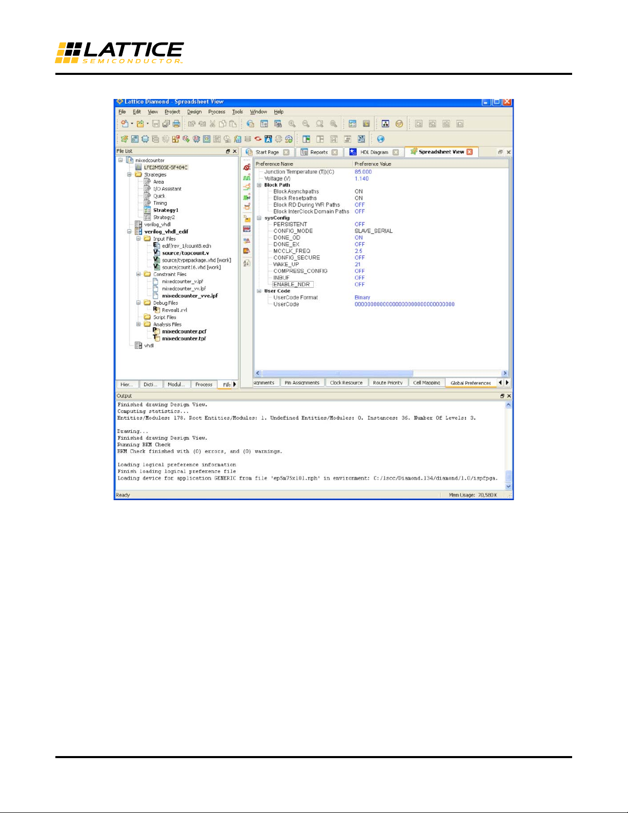
Figure 15-14. Global Preferences Tab
LatticeECP2/M sysCONFIG Usage Guide
Setting Bitstream Generation Options in Diamond
To set any of the Bitstream Generation options listed in Table 15-12, do the following:
• In the File List pane, double-click the left mouse button on a Strategy to invoke the Strategy settings window.
• In the Process pane, left-click on Bitstream. All options related to generating a bitstream can be set in this win-
dow.
15-31
Page 32

Table 15-12. Bitstream Generation Options
Preference Name Values
Disable (default)
Chain Mode
Create bit file True
No Header
Output Format
PROM Data Output Format
Reset Config RAM in re-configuation
Run DRC
Search Path Enter a value or browse to specify the search path
Bypass
Flowthrough
Tr u e
False
Bit File (Binary)
Mask and Readback File (ASCII)
Mask and Radback File (Binary)
Raw Bit file (ASCII)
Intel Hex 32-bit
Motorola Hex 32-bit
Tr u e
False
Tr u e
False
Figure 15-15. Setting Bitstream Options in Diamond
LatticeECP2/M sysCONFIG Usage Guide
• Double-click the left mouse button on the Value you want to set. Select the desired value from the drop-down
menu.
15-32
Page 33

LatticeECP2/M sysCONFIG Usage Guide
Note: An explanation of the option is displayed at the bottom of the window. The Help button also invokes online
help for the option
•Select OK. You can then run the Bitstream File process.
Setting Security Options in Diamond
Prior to setting security options in Diamond, you must have installed the Encryption Control Pack. You must also
have selected an encrypted device in your project.
To Set Security Settings, do the following:
• Select the Tools > Security Setting option. The following dialog box appears:
• If desired, select Change and enter a password.
•Select OK. A dialog window appears to enter an encryption key.
• If you do not want to enable an encryption key, select OK.
• If you do want to enable an encryption key, select the Advanced Security Settings checkbox, enter the Key
Format, and then enter the Encryption Key.
•Select OK to create the encryption files.
15-33
 Loading...