

Page 1

Evaluation Board User Guide
FPGA-EB-02014-1.0
March 2018
DisplayPort VIP Input Board
Page 2

DisplayPort VIP Input Board
Evaluation Board User Guide
Contents
Acronyms in This Document ................................................................................................................................................. 3
1. Introduction .................................................................................................................................................................. 4
1.1. Further Information ................................................................................................................................................ 5
2. Functional Description .................................................................................................................................................. 6
2.1. Switches .................................................................................................................................................................. 6
2.2. DisplayPort Interface .............................................................................................................................................. 6
2.3. LVDS Translator ...................................................................................................................................................... 6
2.4. Clock Interface ........................................................................................................................................................ 6
3. High-Speed Headers ..................................................................................................................................................... 7
4. Power Supply ................................................................................................................................................................ 9
5. User LEDs and Headers ............................................................................................................................................... 10
6. Ordering Information .................................................................................................................................................. 11
References .......................................................................................................................................................................... 12
Technical Support Assistance ............................................................................................................................................. 12
Appendix A. DisplayPort VIP Input Board Schematics ........................................................................................................ 13
Appendix B. DisplayPort VIP Input Board Bill of Materials ................................................................................................. 17
Revision History ................................................................................................................................................................... 20
Figures
Figure 1.1. Top View of DisplayPort VIP Input Board ........................................................................................................... 4
Figure 1.2. Bottom View of DisplayPort VIP Input Board ..................................................................................................... 5
Figure 2.1 Functional Block Diagram .................................................................................................................................... 6
Figure 4.1 Power Supply ....................................................................................................................................................... 9
Figure A.1. Block Diagram ................................................................................................................................................... 13
Figure A.2. DP Redriver and Connector I/F ......................................................................................................................... 14
Figure A.3. Power, Debug LED, Header I/F ......................................................................................................................... 15
Figure A.4. Clock Synthesizer .............................................................................................................................................. 16
Tables
Table 3.1. Connector J1 ........................................................................................................................................................ 7
Table 3.2. Connector J2 ........................................................................................................................................................ 8
Table 5.1 User LEDs............................................................................................................................................................. 10
Table 8.1. Reference Part Number ..................................................................................................................................... 11
All other brand or product names are trademarks or registered trademarks of their respective holders. The specifications and information herein are subject to change without notice.
2 FPGA-EB-02014-1.0
© 2018 Lattice Semiconductor Corp. All Lattice trademarks, registered trademarks, patents, and disclaimers are as listed at www.latticesemi.com/legal.
Page 3
DisplayPort VIP Input Board
Acronym
Definition
DP
DisplayPort
I2C
Inter-Integrated Circuit
LDO
Low Dropout
LED
Light-emitting Diode
LVDS
Low-Voltage Differential Signaling
mDP
Mini DisplayPort
SPI
Serial Peripheral Interface
VIP
Video Interface Platform
Evaluation Board User Guide
Acronyms in This Document
A list of acronyms used in this document.
© 2018 Lattice Semiconductor Corp. All Lattice trademarks, registered trademarks, patents, and disclaimers are as listed at www.latticesemi.com/legal. All other brand or product names are
FPGA-EB-02014-1.0 3
trademarks or registered trademarks of their respective holders. The specifications and information herein are subject to change without notice.
Page 4
DisplayPort VIP Input Board
User LEDs
Mini DisplayPort
Connector
SN75DP130
SN65MLVD200
3.3 V Power to mDP
(Not populated)
SI5342B Clock
Synthesizer
(Not Populated)
User Headers
System Reset
Evaluation Board User Guide
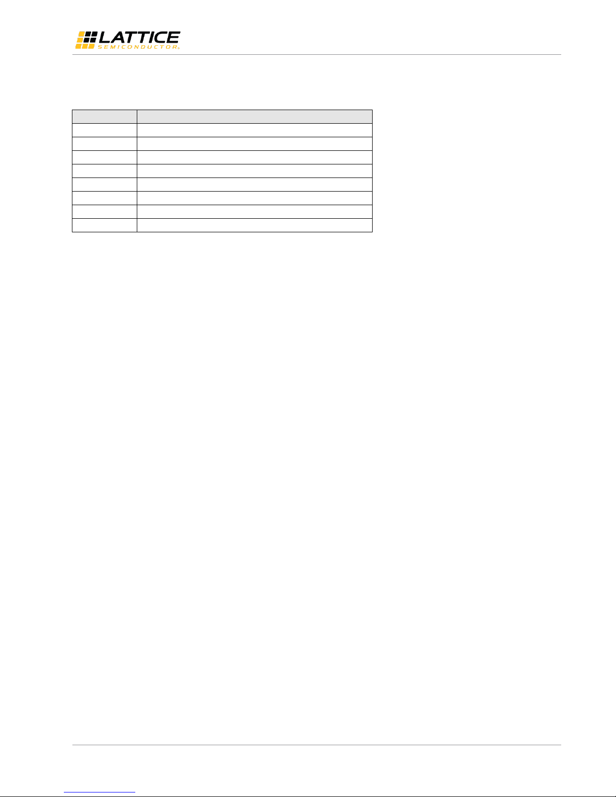
1. Introduction
This document describes the Lattice Semiconductor DisplayPort® VIP Input Board. This board is designed to work with
the Lattice Video Interface Platform (VIP) board interconnect system.
This user guide includes descriptions of board components, schematics, and bill of materials.
Key features of the DisplayPort VIP Input Board include:
Integrated Texas Instruments SN75DP130 DisplayPort 1:1 Redriver
Mini DisplayPort (mDP) connector
Two 60-pin Rugged High-Speed Headers
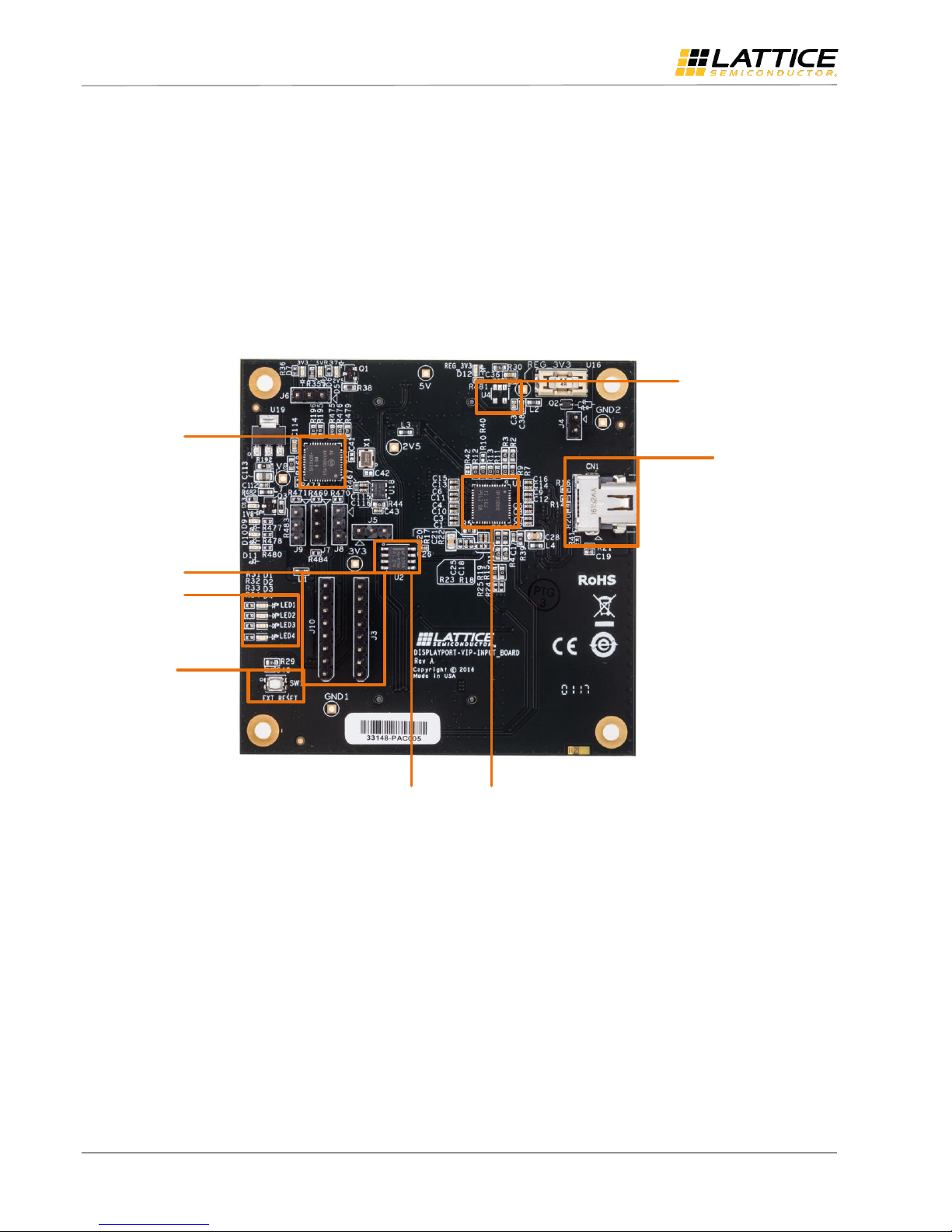
Figure 1.1 shows the top view of the DisplayPort VIP Input Board and its key components. Figure 1.2 shows the bottom
view of the board.
Figure 1.1. Top View of DisplayPort VIP Input Board
All other brand or product names are trademarks or registered trademarks of their respective holders. The specifications and information herein are subject to change without notice.
4 FPGA-EB-02014-1.0
© 2018 Lattice Semiconductor Corp. All Lattice trademarks, registered trademarks, patents, and disclaimers are as listed at www.latticesemi.com/legal.
Page 5
DisplayPort VIP Input Board
Upstream Connector (J1)
Upstream Connector (J2)
Evaluation Board User Guide
Figure 1.2. Bottom View of DisplayPort VIP Input Board
1.1. Further Information
The following references provide detailed information on the DisplayPort VIP Input Board:
Appendix A. DisplayPort VIP Input Board Schematics
Appendix B. DisplayPort VIP Input Board Bill of Materials
For more information on boards and kits available for the VIP (Video Interface Platform) system visit
www.latticesemi.com/boards
For details on the Texas Instruments SN75DP130, visit the Texas Instruments website at www.ti.com
© 2018 Lattice Semiconductor Corp. All Lattice trademarks, registered trademarks, patents, and disclaimers are as listed at www.latticesemi.com/legal. All other brand or product names are
FPGA-EB-02014-1.0 5
trademarks or registered trademarks of their respective holders. The specifications and information herein are subject to change without notice.
Page 6
DisplayPort VIP Input Board
SN75DP130
U1
mDP
Connector
CN1
J1
DisplayPort Main Link
(4 lanes)
Aux Channel
HPD/CAD/Control
DisplayPort Main Link
(4 lanes)
Aux Channel
HPD/CAD/Control
Evaluation Board User Guide
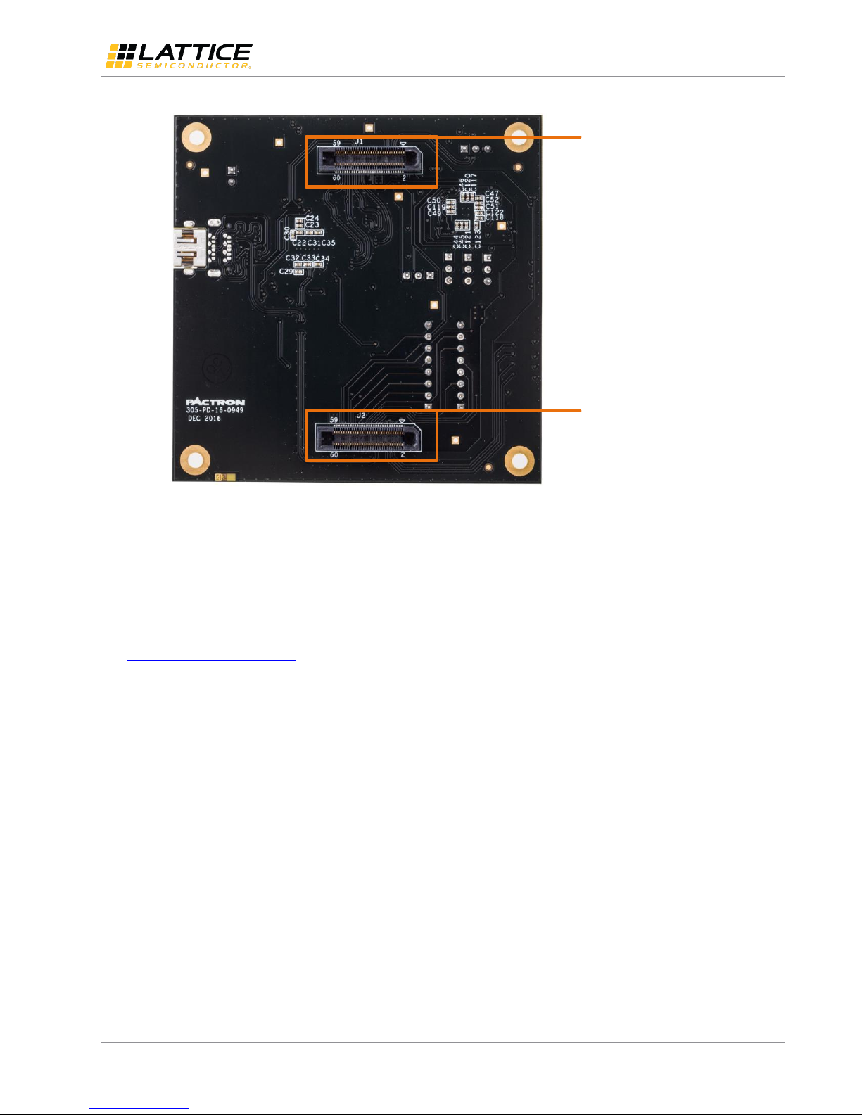
2. Functional Description
The DisplayPort VIP Input Board receives up to 4-lanes of DisplayPort video from the Mini DisplayPort Connector. The
DisplayPort Main Link, Control and Aux Channel are sent through the TI DisplayPort redriver, which regenerates the
DisplayPort high-speed digital link to connector J1.
Figure 2.1 Functional Block Diagram
2.1. Switches
The push button switch, SW1, controls the reset signal RESET. Pressing SW1 provides logic 0 to the SN75DP130 RSTN
pin. RESET is connected to GSRN on connecter J1, allowing SW1 to control the reset signal for other connected boards.
2.2. DisplayPort Interface
The mini DisplayPort connector, CN1, connects the DisplayPort VIP Input Board to a DisplayPort sink. If PWR Out is
required on Pin 20, the user must populate the 3.3 V Low Dropout (LDO) regulator, U4, and short jumper J4.
2.3. LVDS Translator
The SN65MLV200 LVDS (Low-Voltage Differential Signaling) Driver/Receiver, U2, can be used to translate the LVDS AUX
Channel to single ended I/O. This can be used if the downstream processor board is unable to receive LVDS. The single
ended I/O are routed to connector J2.
2.4. Clock Interface
The DisplayPort VIP Input Board provides the ability to add advanced clock circuitry, allowing the user to provide a fine
tunable reference clock to the downstream board. This is done by populating U17 with a Silicon Labs Si5342B, High
Performance Jitter Attenuator Clock Multiplier. The device can be programmed from the downstream connector using
an I2C (Inter Integrated Circuit) or SPI (Serial Peripheral Interface) interface.
© 2018 Lattice Semiconductor Corp. All Lattice trademarks, registered trademarks, patents, and disclaimers are as listed at www.latticesemi.com/legal.
All other brand or product names are trademarks or registered trademarks of their respective holders. The specifications and information herein are subject to change without notice.
6 FPGA-EB-02014-1.0
Page 7
DisplayPort VIP Input Board
J1 Connector Pin
Signal Name
SN75DP130 pin
Description
1
3.3V — —
2
5V — — 3 3.3V — — 4 5V — — 5 GND — —
6
5V — —
7
LVDS_P
—
LVDS Reference Clock from Si5342
8
GND — — 9 LVDS_N
—
LVDS Reference Clock from Si5342
11
GND — —
13
AUX_P
AUX_SRCp
DisplayPort Auxiliary Data Channel
14
GND — —
15
AUX_N
AUX_SRCn
DisplayPort Auxiliary Data Channel
17
GND — —
20
GND — —
22
2.5V — —
23
GND — —
24
2.5V — —
25
GND — —
26
GND — —
28
RESET
RSTN
Global System Reset
30
HPD_SINK
HPD_SINK
Hot Plug Detect
32
CAD_SINK
CAD_SINK
DP Cable Adapter Detect
34
GND — —
36
RXP0_D1CH0
OUT2p
DisplayPort Main Link Lane 0
38
RXN0_D1CH0
OUT2n
DisplayPort Main Link Lane 0
40
GND — —
41
SCL_CTL
SCL_CTL
I2C Interface to SN75DP130
42
RXP0_D1CH1
OUT3p
DisplayPort Main Link Lane 1
43
SDA_CTL
SDA_CTL
I2C Interface to SN75DP130
44
RXN0_D1CH1
OUT3n
DisplayPort Main Link Lane 1
46
GND — —
48
RXP0_D0CH0
OUT0p
DisplayPort Main Link Lane 0
50
RXN0_D0CH0
OUT0n
DisplayPort Main Link Lane 0
52
GND — —
54
RXP0_D0CH1
OUT1p
DisplayPort Main Link Lane 1
55
GND — —
56
RXN0_D0CH1
OUT1n
DisplayPort Main Link Lane 1
57
GND — —
58
GND — —
59
GND — —
10, 12, 60, 16, 18, 19, 21, 27,
29, 31, 33, 35, 37, 39, 45, 47,
49, 51, 53
Not Connected
—
—
Evaluation Board User Guide
3. High-Speed Headers
The two 60-pin high-speed headers, connectors J1 and J2, are used to connect to a downstream host processor board.
Table 3.1. Connector J1
© 2018 Lattice Semiconductor Corp. All Lattice trademarks, registered trademarks, patents, and disclaimers are as listed at www.latticesemi.com/legal. All other brand or product names are
FPGA-EB-02014-1.0 7
trademarks or registered trademarks of their respective holders. The specifications and information herein are subject to change without notice.
Page 8

DisplayPort VIP Input Board
J1 Connector Pin
Signal Name
SN75DP130 pin
Description
1
3.3V — — 2 3.3V — — 3 3.3V — — 4 3.3V — — 7 AUX_EN
—
Aux Channel Translator Enable
8
LED1
—
User LED
9
AUX_OUT
—
Aux Channel single ended Out
10
LED2
—
User LED
11
AUX_IN
—
Aux Channel single ended In
12
LED3
—
User LED
13
EN
EN
SN75DP130 Enable
14
LED4
—
User LED
17
GND — —
18
GND — —
19
GND — —
20
GND — —
21
SPI_CSN
—
Si5342 I2C/SPI Interface
22
GND — —
23
SPI_CLK
—
Si5342 I2C/SPI Interface
24
RX_SENSEP
—
—
25
SPI_MOSI
—
Si5342 I2C/SPI Interface
26
RX_SENSEN
— — 27
SPI_MISO
—
Si5342 I2C/SPI Interface
29
INT_N
—
Si5342 Interrupt
30
SDA_DDC
SDA_DDC
I2C Display Data Channel
31
OE_N
—
Si5342 Output Enable
32
SCL-DDC
SCL_DDC
I2C Display Data Channel
33
GND — —
35
GND — —
36
GND — —
38
GND — —
39
HEADER1
—
User I/O Header J3
40
GND — —
41
HEADER2
—
User I/O Header J3
43
HEADER3
—
User I/O Header J3
45
HEADER4
—
User I/O Header J3
47
HEADER5
—
User I/O Header J3
51
CMOS_CLK
—
Reference Clock from Si5342
53
GND — —
54
GND — —
55
GND — —
56
GND — —
57
2.5V — —
58
2.5V — —
59
2.5V — —
60
2.5V — —
5, 6, 15, 16, 28, 34, 37, 42, 44,
46, 48, 49, 50, 52
Not Connected
—
—
Evaluation Board User Guide
Table 3.2. Connector J2
All other brand or product names are trademarks or registered trademarks of their respective holders. The specifications and information herein are subject to change without notice.
8 FPGA-EB-02014-1.0
© 2018 Lattice Semiconductor Corp. All Lattice trademarks, registered trademarks, patents, and disclaimers are as listed at www.latticesemi.com/legal.
Page 9

DisplayPort VIP Input Board
5 V from J1
3.3 V from J1/J2
2.5 V from J1/J2
Status
LED D7
Status
LED D5
Status
LED D6
LDO*
U4
mDP
Connector
CN1
3.3 V, 500 mA
* Not Installed
J4
LDO
U19
Status
LED D13
1.8 V, 500 mA
Status
LED D12
Evaluation Board User Guide
4. Power Supply
Board power is supplied through connectors J1 and J2. Figure 4.1 shows the power distribution scheme. To provide
power to the mini DisplayPort connector, install a 5.0 V to 3.3 V LDO at U4 and add shunt to jumper J4.
Figure 4.1 Power Supply
© 2018 Lattice Semiconductor Corp. All Lattice trademarks, registered trademarks, patents, and disclaimers are as listed at www.latticesemi.com/legal. All other brand or product names are
FPGA-EB-02014-1.0 9
trademarks or registered trademarks of their respective holders. The specifications and information herein are subject to change without notice.
Page 10

DisplayPort VIP Input Board
Signal
LED #
Connector J2 Pin
Color
LED1
D1
8
Green
LED2
D2
10
Green
LED3
D3
12
Green
LED4
D4
14
Green
Signal
Header J3 Pin
Connector J2 Pin
3V3
1
—
HEADER1 2 39
HEADER2 3 41
HEADER3 4 48
HEADER4 5 45
HEADER5 6 47
RESET
7
—
GND
8
—
Signal
Header J10 Pin
Connector J2 Pin
3V3
1
—
SPI_CSN 2 21
SPI_MISO 3 23
SPI_MOSI 4 25
SPI_CLK 5 27
INT_N
6
29
OE_N
7
31
GND
8
—
Evaluation Board User Guide
5. User LEDs and Headers
Four discrete LEDs (light-emitting diodes) are available to the user. These are driven by the downstream processor
board through connector J2.
Table 5.1 User LEDs
Two 8-pin 100-mil headers, J3 and J10, are included on the board. Header J3 provides five user connections which are
routed to the downstream connector J2. Header J10 provides an external interface to the Si5342, U17 (not installed),
but can also be used to provide user interface to the downstream connector J2.
Table 5.2 Header J3
Table 5.3 Header J10
All other brand or product names are trademarks or registered trademarks of their respective holders. The specifications and information herein are subject to change without notice.
10 FPGA-EB-02014-1.0
© 2018 Lattice Semiconductor Corp. All Lattice trademarks, registered trademarks, patents, and disclaimers are as listed at www.latticesemi.com/legal.
Page 11

DisplayPort VIP Input Board
Description
Ordering Part Number
DisplayPort VIP Input Board
DP-VIP-I-EVN
Evaluation Board User Guide
6. Ordering Information
Please visit www.latticesemi.com/boards for the latest ordering information.
Table 6.1. Reference Part Number
© 2018 Lattice Semiconductor Corp. All Lattice trademarks, registered trademarks, patents, and disclaimers are as listed at www.latticesemi.com/legal. All other brand or product names are
FPGA-EB-02014-1.0 11
trademarks or registered trademarks of their respective holders. The specifications and information herein are subject to change without notice.
Page 12

DisplayPort VIP Input Board
Evaluation Board User Guide
References
For more information, refer to
Lattice Embedded Vision Development Kit User Guide (FPGA-UG-02015)
ECP5 VIP Processing Board (FPGA-EB-02001)
Technical Support Assistance
Submit a technical support case through www.latticesemi.com/techsupport.
All other brand or product names are trademarks or registered trademarks of their respective holders. The specifications and information herein are subject to change without notice.
12 FPGA-EB-02014-1.0
© 2018 Lattice Semiconductor Corp. All Lattice trademarks, registered trademarks, patents, and disclaimers are as listed at www.latticesemi.com/legal.
Page 13

DisplayPort VIP Input Board
Evaluation Board User Guide
© 2018 Lattice Semiconductor Corp. All Lattice trademarks, registered trademarks, patents, and disclaimers are as listed at www.latticesemi.com/legal.
All other brand or product names are trademarks or registered trademarks of their respective holders. The specifications and information herein are subject to change without notice.
FPGA-EB-02014-1.0 13
Appendix A. DisplayPort VIP Input Board Schematics
Figure A.1. Block Diagram
5
5
4
4
3
3
2
2
1
1
D D
C C
B B
A A
DisplayPort VIP Input Board
LED & Header I/F
SN75DP130
GPIO I/F
5V,3V3,2V5
Downstream Connector 1&2
I2C
X4 DP Data
DP AUX I/F
Control GPIO
OnBoard LDO
(pg4)
(pg4)
(pg3&4)
Mini DP Connector
X4 DP Data
(pg3)
(pg3)
(pg5)
Clock Synthesizer
Date:
Size
Schematic Rev
ofSheet
Title
Lattice Semiconductor Applications
Email: techsupport@Latticesemi.com
Board Rev
Project
Friday, 11-Nov-16
B
0.1
52
Title & Index
DisplayPort VIP Input Board
A
Date:
Size
Schematic Rev
ofSheet
Title
Lattice Semiconductor Applications
Email: techsupport@Latticesemi.com
Board Rev
Project
Friday, 11-Nov-16
B
0.1
52
Title & Index
DisplayPort VIP Input Board
A
Date:
Size
Schematic Rev
ofSheet
Title
Lattice Semiconductor Applications
Email: techsupport@Latticesemi.com
Board Rev
Project
Friday, 11-Nov-16
B
0.1
52
Title & Index
DisplayPort VIP Input Board
A
Page 14

DisplayPort VIP Input Board
Evaluation Board User Guide
© 2018 Lattice Semiconductor Corp. All Lattice trademarks, registered trademarks, patents, and disclaimers are as listed at www.latticesemi.com/legal.
All other brand or product names are trademarks or registered trademarks of their respective holders. The specifications and information herein are subject to change without notice.
14 FPGA-EB-02014-1.0
Figure A.2. DP Redriver and Connector I/F
5
5
4
4
3
3
2
2
1
1
D D
C C
B B
A A
PLACE DE-CAPS CLOSE TO THEIR POWER PINS
3V3
3V3_EXT 5V
2V5_EXT
3V3_RX
DP_3V3
3V3
3V3_RX
3V3
3V3
3V3
3V3
RESET {3,4,5}
AUX_IN{4}
SDA_DDC {4}
SCL_DDC {4}
AUX_OUT{4}
EN {4}
AUX_EN {4}
RX_SENSEP {4}
RX_SENSEN {4}
RESET {3,4,5}
LVDS_P{5}
LVDS_N{5}
Date:
Size
Schematic Rev
ofSheet
Title
Lattice Semiconductor Applications
Email: techsupport@Latticesemi.com
Board Rev
Project
Friday, 11-Nov-16
B
0.1
53
DP Redriver & Connector I/F
DisplayPort VIP Input Board
A
Date:
Size
Schematic Rev
ofSheet
Title
Lattice Semiconductor Applications
Email: techsupport@Latticesemi.com
Board Rev
Project
Friday, 11-Nov-16
B
0.1
53
DP Redriver & Connector I/F
DisplayPort VIP Input Board
A
Date:
Size
Schematic Rev
ofSheet
Title
Lattice Semiconductor Applications
Email: techsupport@Latticesemi.com
Board Rev
Project
Friday, 11-Nov-16
B
0.1
53
DP Redriver & Connector I/F
DisplayPort VIP Input Board
A
C33
100nF
C10 100nF
R2
4.7k
C12 100nFC11 100nF
C22
100nF
R4
4.7k
R3
4.7k
R25 10K
R130
C13 100nF
R60 R70
C19
1uF
R17
2.49K
C31
100nF
E-PAD(GND)
U1
SN75DP130SS
VCC
1
VDDD_DREG
2
ADDR_EQ
3
SCL_CTL
4
SDA_CTL
5
VCC
6
NC1
7
CAD_SRC
8
HPD_SRC
9
CAD_SINK
10
HPD_SINK
11
VCC
12
OUT3n
13
OUT3p
14
NC2
15
OUT2n
16
OUT2p
17
GND
18
OUT1n
19
OUT1p
20
NC3
21
OUT0n
22
OUT0p
23
GND
24
VCC
25
EN
26
AUX_SINKn
27
AUX_SINKp
28
AUX_SRCn
29
AUX_SRCp
30
GND
31
VCC
32
SCL_DDC
33
SDA_DDC
34
RSTn
35
VCC
36
NC7
37
IN0p
38
IN0n
39
NC6
40
IN1p
41
IN1n
42
NC5
43
IN2p
44
IN2n
45
NC4
46
IN3p
47
IN3n
48
EP
49
R120
R50
C29
1uF
C16 100nF
U2
SN65MLVD200
4
D
1
R
7
B
6
A
3DE8
VCC
5
GND
RE#
2
C28
10uF
R18
51E
C7 100nF
R190
C35
100nF
C8 100nF
R21
1M
C18 0.1uF
C25 0.1uF
C26
0.1uF
C3 100nF
L1
60ohms 2.3A
12
C2 100nF
C24
1uF
L4
60ohms 2.3A
12
C34
100nF
C4 100nF
J1
ERF5-030-07.0-L-DV-K-TR
2
4
6
8
10
12
14
16
18
20
22
24
26
28
30
32
34
36
38
40
42
44
46
48
50
52
54
56
58
60
1
3
5
7
9
11
13
15
17
19
21
23
25
27
29
31
33
35
37
39
41
43
45
47
49
51
53
55
57
59
C17 1uF
R16
1M
R150
R40 1M
DNI
C9 100nFC6 100nF
R1
4.7k
C23
100nF
C21
0.1uF
R110
R80 R90
C30
100nF
C15 100nF
CN1
Mini-DP
DPPOWER
20
GND3
19
AUX_CHN
18
ML_LANE1P
17
AUX_CHP
16
ML_LANE1N
15
GND2
14
GND1
13
ML_LANE0P
12
ML_LANE2P
11
ML_LANE0N
10
ML_LANE2N
9
GND5
8
GND4
7
CONFIG2
6
ML_LANE3P
5
CONFIG1
4
ML_LANE3N
3
HPD
2
GND6
1
SHLD121SHLD222SHLD323SHLD4
24
C14 100nF
R100
C32
100nF
R390
R23
51E
R42
100K
DNI
C20
10uF
R41
100K
R24 10K
R14
1M
C5 100nF
C1 100nF
R20
100K
DNI
R22
1.5K
RXP0_D0CH0
RXN0_D0CH0
RXP0_D0CH1
RXN0_D0CH1
RXP0_D1CH0
RXN0_D1CH0
RXP0_D1CH1
RXN0_D1CH1
HPD_SRC
RST_N
SCL_CTL
SDA_CTL
CAD_SRC
HPD_SRC
RXN0_D0CH1
RXP0_D0CH1
RXN0_D1CH1
RXP0_D1CH1
RXN0_D1CH0
RXP0_D1CH0
RXP0_D0CH0
RXN0_D0CH0
AUX_P
AUX_N
AUX_P
AUX_N
AUX_P
AUX_N
HPD_SINK
CAD_SINK
SCL_CTL
SDA_CTL
SDA_DDC
SCL_DDC
SDA_DDC
SCL_DDC
CAD_SINK
HPD_SINK
CAD_SRC
SCL_CTL
SDA_CTL
Page 15

DisplayPort VIP Input Board
Evaluation Board User Guide
© 2018 Lattice Semiconductor Corp. All Lattice trademarks, registered trademarks, patents, and disclaimers are as listed at www.latticesemi.com/legal.
All other brand or product names are trademarks or registered trademarks of their respective holders. The specifications and information herein are subject to change without notice.
FPGA-EB-02014-1.0 15
Figure A.3. Power, Debug LED, Header I/F
5
5
4
4
3
3
2
2
1
1
D D
C C
B B
A A
NOTE : PLACE SWITCH IN THE TOP SIDE
EXTERNAL RESET
500mA traces
700mA traces
500mA traces
3V3
3V33V33V33V3
5V 3V3 5V
2V5
3V3_EXT 3V3_EXT
2V5_EXT
2V5_EXT2V5
3V3
5V REG_3V3 DP_3V3
5V
3V3
REG_3V3
2V5
1V8
5V
1V8
1V8
5V
REG_3V3
RX_SENSEP {3}
RX_SENSEN {3}
AUX_IN{3}
AUX_EN{3}
AUX_OUT{3}
EN{3}
SDA_DDC {3}
SCL_DDC {3}
RESET {3,5}
SPI_CSN{5}
SPI_CLK{5}
SPI_MOSI{5}
SPI_MISO{5}
INT_N{5}
OE_N{5}
CMOS_CLK{5}
Date:
Size
Schematic Rev
ofSheet
Title
Lattice Semiconductor Applications
Email: techsupport@Latticesemi.com
Board Rev
Project
Friday, 11-Nov-16
B
0.1
54
Power,Debug LED,Header I/F
DisplayPort VIP Input Board
A
Date:
Size
Schematic Rev
ofSheet
Title
Lattice Semiconductor Applications
Email: techsupport@Latticesemi.com
Board Rev
Project
Friday, 11-Nov-16
B
0.1
54
Power,Debug LED,Header I/F
DisplayPort VIP Input Board
A
Date:
Size
Schematic Rev
ofSheet
Title
Lattice Semiconductor Applications
Email: techsupport@Latticesemi.com
Board Rev
Project
Friday, 11-Nov-16
B
0.1
54
Power,Debug LED,Header I/F
DisplayPort VIP Input Board
A
D3
Green
12
D6
Green
12
C39
0.1uF
J3
8 HEADER
1
2
3
4
5
6
7
8
R192 0
D7
Green
12
R30
4.7k
R29
4.7k
R32
330E
C113
22uF
1K
R482
D2
Green
12
C40
0.1uF
D13
Green
12
R483 10K
GND2
1
R31
330E
L3
60ohms 2.3A
12
SW1
SYS_RST
12
34
R481
330E
D1
Green
12
TH1
ThruHole
Q3
MMBT2222A
32
1
D5
Green
12
C114
10uF
GND1
1
U16
FUSE
112
2
1K
R37
D12
Green
12
1V8
1
J2
ERF5-030-07.0-L-DV-K-TR
2
4
6
8
10
12
14
16
18
20
22
24
26
28
30
32
34
36
38
40
42
44
46
48
50
52
54
56
58
60
1
3
5
7
9
11
13
15
17
19
21
23
25
27
29
31
33
35
37
39
41
43
45
47
49
51
53
55
57
59
TH4
ThruHole
R38 10K
TH2
ThruHole
U4 XC6222B331MR-G
DNI
Vin
1
Vss
2
CE3NC
4
Vout
5
2V5
1
Q1
MMBT2222A
32
1
3V3
1
R34
330E
U19
NCP1117ST18T3G
GND
1
IN3OUT
2
TAB
4
Q2
D1213A-01WS-7
R36
330E
TH3
ThruHole
C36
10uF
REG_3V3
1
D4
Green
12
C112
0.1uF
5V
1
C37
0.1uF
R35
1K
J4
Jumper
1 2
R33
330E
C38
10uF
L2
60ohms 500mA
12
L7
600ohm 500mA
12
RESET
LED1
LED2
LED3
LED4
HEADER1
HEADER3
HEADER2
HEADER4
HEADER5
LED1
LED2
LED3
LED4
HEADER1
HEADER2
HEADER3
HEADER4
HEADER5
RESET
Page 16

DisplayPort VIP Input Board
Evaluation Board User Guide
© 2018 Lattice Semiconductor Corp. All Lattice trademarks, registered trademarks, patents, and disclaimers are as listed at www.latticesemi.com/legal.
All other brand or product names are trademarks or registered trademarks of their respective holders. The specifications and information herein are subject to change without notice.
16 FPGA-EB-02014-1.0
Figure A.4. Clock Synthesizer
5
5
4
4
3
3
2
2
1
1
D D
C C
B B
A A
Place 1uF capacitor closer to each power pin
Place C42,C41 such a that
it doesnt create stub when
its DNI
3V3
3V3
3V3
1V8
3V3
3V3
2V5
3V3 2V5
3V3
3V3
3V3
3V3
OE_N {4}
LVDS_P {3}
LVDS_N {3}
CMOS_CLK {4}
SPI_CSN { 4}
SPI_MISO {4}
SPI_CLK {4}
SPI_MOSI {4}
RESET {3,4}
INT_N {4}
Date:
Size
Schematic Rev
ofSheet
Title
Lattice Semiconductor Applications
Email: techsupport@Latticesemi.com
Board Rev
Project
Friday, 11-Nov-16
B
0.1
55
CLOCK SYNTHESIZER
DisplayPort VIP Output Board
A
Date:
Size
Schematic Rev
ofSheet
Title
Lattice Semiconductor Applications
Email: techsupport@Latticesemi.com
Board Rev
Project
Friday, 11-Nov-16
B
0.1
55
CLOCK SYNTHESIZER
DisplayPort VIP Output Board
A
Date:
Size
Schematic Rev
ofSheet
Title
Lattice Semiconductor Applications
Email: techsupport@Latticesemi.com
Board Rev
Project
Friday, 11-Nov-16
B
0.1
55
CLOCK SYNTHESIZER
DisplayPort VIP Output Board
A
C120
1uF
J5
CON3
1
2
3
1KR484
C42 18pF
DNI
C41 18pF
DNI
1K
R471
R467
100E
R4680
R478 330E
C115 100nF
C122
1uF
J8
CON3
1
2
3
C121
1uF
J10
8 HEADER
1
2
3
4
5
6
7
8
C44
100nF
C50
1uF
C118
1uF
R477 330E
C119
1uF
R480 330E
E-PAD
U17
SI5342B-B-GM
IN1
1
IN1B
2
IN_SEL0
3
X1
4
XA
5
XB
6
X2
7
VDDA18VDDA2
9
IN2
10
IN2B
11
OEb12SDA/SDIO13SCLK14A1/SDO15A0/CSB16RSTb
17
VDDO0
18
OUT0b
19
OUT0
20
VDD3
21
NC
22
VDDO1
23
OUT1b
24
OUT1
25
VDDS1
26
LOLb
27
LOS_XAXBb
28
VDDS2
29
LOS0b
30
LOS1b
31
VDD4
32
INTRb
33
VDDS3
34
LOS2b
35
LOS3b
36
IN_SEL1
37
I2C_SEL
38
VDD239VDD1
40
IN3/FB_IN
41
IN3b/FB_INb
42
IN0
43
IN0b
44
EPAD
45
C47
1uF
C46
100nF
U18
DSC1103CE2-135.0000
EN
1
NC2GND
3
OUT_P
4
OUT_N
5
VDD
6
C117
1uF
J9
CON3
1
2
3
R1950
R476
4.7k
C49
100nF
C43
0.1uF
R44 4.7k
C116 100nF
R1960
D10 Green
1 2
J6
CON3
123
1K
R473
C123
1uF
X1
54Mhz
1
1
3
3
G1
2
G2
4
1K
R470
R475
4.7k
C52
1uF
D9 Green
1 2
C51
100nF
1K
R469
D11 Green
1 2
C45
1uF
J7
CON3
1
2
3
R479
4.7k
SPI_CSN
SPI_MISO
SPI_MOSI
SPI_CLK
INT_N
OE_N
SPI_MOSI
SPI_CLK
OE_N
SPI_MISO
SPI_CSN
INT_N
Page 17

DisplayPort VIP Input Board
Evaluation Board User Guide
© 2018 Lattice Semiconductor Corp. All Lattice trademarks, registered trademarks, patents, and disclaimers are as listed at www.latticesemi.com/legal.
All other brand or product names are trademarks or registered trademarks of their respective holders. The specifications and information herein are subject to change without notice.
FPGA-EB-02014-1.0 17
Appendix B. DisplayPort VIP Input Board Bill of Materials
Item
Reference
Qty
Value
Comments
Part Number
Manufacturer
Description
1
CN1 1 Mini-DP
—
2129320-3
TE Connectivity
MINI DISPLAYPORT REVERSE OFFSET
2
C1,C2,C3,C4,C5,C6,C7,C8,
C9,C10,C11,C12,C13,C14,
C15,C16,C115,C116
18
100 nF
—
885012205018
Wurth
CAP CER 0.1UF 10V X7R 0402
3
C17,C19,C24,C29,C45,C47,
C50,C52,C117,C118,C119,
C120,C121,C122,C123
15
1 uF — GRM155R61A105KE15D
Murata
CAP CER 1UF 10V 10% X5R 0402
4
C18,C21,C25,C26,C43
5
0.1 uF — GRM155R61A104KA01D
Murata
CAP CER 0.1UF 10V X5R 0402
5
C20,C28
2
10 uF — GRM21BR61A106KE19L
Murata
CAP CER 10UF 10V 10% X5R 0805
6
C22,C23,C30,C31,C32,C33,
C34,C35,C44,C46,C49,C51
12
100 nF
—
GRM155R61A104KA01D
Murata
CAP CER 0.1UF 10V X5R 0402
7
C36,C38
2
10 uF — CL10X106MP8NRNC
Samsung
CAP CER 10UF 10V 20% X6S 0603
8
C37,C39
2
0.1 uF — CL05A104MP5NNNC
Samsung
CAP CER 0.1UF 10V X5R 0402
9
C40 1 0.1 uF — 885012205037
Wurth
CAP CER 0.1UF 16V X7R 0402
10
C41,C42
2
18 pF
DNL
C0402C180K3GACTU
Kemet
CAP CER 18PF 25V C0G 0402
11
C112 1 0.1 uF — C0402C104K4RACTU
Kemet
CAP CER 0.1UF 16V X7R 0402
12
C113 1 22 uF — LMK212BJ226MG-T
Taiyo Yuden
CAP CER 22UF 10V X5R 0805
13
C114 1 10 uF — LMK107BJ106MALTD
Taiyo Yuden
CAP CER 10UF 10V X5R 0603
14
D1,D2,D3,D4,D5,D6,D7,D9,
D10,D11,D12,D13
12
Green — LTST-C190KGKT
LITE-On Inc
LED GREEN CLEAR 0603 SMD
15
GND1,GND2,5V,1V8,2V5,
REG_3V3,3V3
7
TP
DNL
— — —
16
J1,J2 2 —
—
ERF5-030-07.0-L-DV-KTR
Samtec Inc
Conn High Speed Edge Rate Terminal
Strip HDR 60 POS
0.5 mm Solder ST SMD T/R -
Page 18

DisplayPort VIP Input Board
Evaluation Board User Guide
© 2018 Lattice Semiconductor Corp. All Lattice trademarks, registered trademarks, patents, and disclaimers are as listed at www.latticesemi.com/legal.
All other brand or product names are trademarks or registered trademarks of their respective holders. The specifications and information herein are subject to change without notice.
18 FPGA-EB-02014-1.0
Item
Reference
Qty
Value
Comments
Part Number
Manufacturer
Description
17
J3,J10 2 8 HEADER
—
— — —
18
J4 1 Jumper
—
— — —
19
J5,J6,J7,J8,J9
5
CON3 — — — —
20
L1,L3,L4
3
60 Ω 2.3 A
—
MPZ1608Y600B
TDK
FERRITE BEAD 60 OHM 0603 1LN
21
L2 1 60 Ω 500 mA
—
MMZ1608Y600B
TDK
FERRITE BEAD 60 OHM 0603 1LN
22
L7 1 600 Ω 500 mA
—
BLM18AG601SN1D
Murata
FERRITE BEAD 600 OHM 0603 1LN
23
Q1,Q3 2 MMBT2222A
—
MMBT2222A,215
NXP USA Inc.
TRANS NPN 40V 0.6A SOT23
24
Q2 1 D1213A-01WS-7
—
D1213A-01WS-7
Diodes
Incorporated
TVS DIODE 3.3VWM 10VC SOD323
25
R1,R2,R3,R4,R29,R30,R44,
R475,R476,R479
10
4.7 k — CRCW06034K70FKEA
Vishay
RES SMD 4.7K OHM 1% 1/10W 0603
26
R5,R6,R7,R8,R9,R10,R11,R
12,R13,R15,R19,R39,R192,
R195,R196,R468
16 0 —
RC0603JR-070RL
Yageo
RES SMD 0.0OHM JUMPER 1/10W 0603
27
R14,R16,R21
3
1 M — ERJ-2GEJ105X
Panasonic
RES SMD 1M OHM 5% 1/10W 0402
28
R17 1 2.49 K — ERA-2AEB2491X
Panasonic
RES SMD 2.49KOHM 0.1% 1/16W 0402
29
R18,R23
2
51E — ERJ-2GEJ510X
Panasonic
RES SMD 51 OHM 5% 1/10W 0402
30
R20,R42
2
100 K
DNL
ERA-2AEB104X
Panasonic
RES SMD 100K OHM 0.1% 1/16W 0402
31
R22 1 1.5 K — ERJ-2RKF1501X
Panasonic
RES SMD 1.5K OHM 1% 1/10W 0402
32
R24,R25
2
10 K — RMCF0402JT10K0
Stackpole
Electronics Inc
RES SMD 10K OHM 5% 1/16W 0402
33
R31,R32,R33,R34,R36,R47
7,R478,R480,R481
9
330E — CRCW0402330RFKED
Vishay Dale
RES SMD 330 OHM 1% 1/16W 0402
34
R35 1 1 K — RC0603FR-071KL
Yageo
RES SMD 1K OHM 1% 1/10W 0603
Page 19

DisplayPort VIP Input Board
Evaluation Board User Guide
© 2018 Lattice Semiconductor Corp. All Lattice trademarks, registered trademarks, patents, and disclaimers are as listed at www.latticesemi.com/legal.
All other brand or product names are trademarks or registered trademarks of their respective holders. The specifications and information herein are subject to change without notice.
FPGA-EB-02014-1.0 19
Item
Reference
Qty
Value
Comments
Part Number
Manufacturer
Description
35
R37,R469,R470,R471,R473,
R482,R484
7
1 K — RMCF0402JT1K00
Stackpole
Electronics Inc
RES SMD 1K OHM 5% 1/16W 0402
36
R38,R483
2
10 K — ERJ-3EKF1002V
Panasonic
RES SMD 10K OHM 1% 1/10W 0603
37
R40 1 1 M
DNL
ERJ-2GEJ105X
Panasonic
RES SMD 1M OHM 5% 1/10W 0402
38
R41 1 100 K — ERA-2AEB104X
Panasonic
RES SMD 100K OHM 0.1% 1/16W 0402
39
R467 1 100E — TNPW0402100RBEED
Vishay
RES SMD 100 OHM 0.1% 1/16W 0402
40
SW1 1 SYS_RST
—
434153017835
Wurth
SWITCH TACTILE SPST-NO 0.05A 12V
41
TH1,TH2,TH3,TH4
4
ThruHole
DNL
— — —
42
U1 1 SN75DP130SS
—
SN75DP130SSRGZR
Texas Instruments
IC DISPLYPRT 1:1 REDRIVR 48VQFN
43
U2 1 SN65MLVD200
—
SN65MLVD200AD
Texas Instruments
IC LVDS LINE DVR/RCVR 8-SOIC
44
U4 1 XC6222B331MR-G
DNL
XC6222B331MR-G
Torex
Semiconductor Ltd
IC REG LDO 3.3V 0.7A SOT25
45
U16 1 FUSE — 0154004.DRT
Littelfuse
FUSE BRD MNT 4A 125VAC/VDC 2SMD
46
U17 1 SI5342B-B-GM
DNL
SI5342B-B-GM
Silicon
Laboratories
IC CLK BUFFER PLL 44QFN
47
U18
1
DSC1103CE2-
135.0000
DNL
DSC1103CE2-135.0000
Microchip
Technology Inc
OSC MEMS 135.000MHZ LVDS SMD
48
U19 1 NCP1117ST18T3G
—
NCP1117ST18T3G
On Semi
IC REG LDO 1.8V 1A SOT223
49
X1 1 54 MHz
—
CX3225SB54000D0WPT
C1
AVX Corp/Kyocera
Corp
CRYSTAL 54MHZ 8PF SMD
50
DISPLAYPORT-VIP-INPUT
BOARD REV1 PCB
1 — —
305-PD-16-0949
PACTRON
Page 20

DisplayPort VIP Input Board
Date
Version
Change Summary
March 2018
1.0
Initial release.
Evaluation Board User Guide
Revision History
All other brand or product names are trademarks or registered trademarks of their respective holders. The specifications and information herein are subject to change without notice.
20 FPGA-EB-02014-1.0
© 2018 Lattice Semiconductor Corp. All Lattice trademarks, registered trademarks, patents, and disclaimers are as listed at www.latticesemi.com/legal.
Page 21

7th Floor, 111 SW 5th Avenue
Portland, OR 97204, USA
T 503.268.8000
www.latticesemi.com
 Loading...