

LaserVision VP415 Service Manual

~@[fWO©@
~@[fWO©@
LaserVision ROM disc drive
VP415/001os1as
Service
LaserVision
ervice Manual
The VP415 is a professional Video Disc Drive for use
computerized audiovisual systems, involving a high
degree of interactivity.
The Drive
optical video discs, according to the LaserVision system
(PAL standard) and it has the capacity to handle
LV-ROM (LaserVision Read Only Memory) interactive
discs.
is
suitable for playback
of
pre-recorded
in
L\fRDM
The differences between /00, /05 and/35 are only related
to the ornamental plate
mainscord.
Version /00
= LV-ROM Disc Drive with Euro mainscord.
= BBC Domesday version with
/05
mainscord
/35
= /00 with
on
the front panel and to the
GB
mainscord
GB
Contents:
Chapter 1
Chapter 2 Remarks
Caution
"Use of controls or adjustments
procedures other than those specified here
in
hazardous ratliation exposure".
Safety regulations require that the set be restored to its original
condition and that parts which are identical with those specified
used.
Technical data
Controls, indicators, connections
Connector pinning
Warnings
Modification levels
Adjustments
Demounting instructions
Service hints
Service tools
List of used symbols
Connections of semiconductors
or
performance
in
may result
of
be
Chapter 3 Module- and connector
Chapter 4 Survey
Chapter 5 Exploded view drawings
Chapter 6 Repair method
Chapter 7 Circuit description
Chapter 8 Service Information
Signal listing
Wiring diagram
Blockdiagram Control routes
Blockdiagram AUDIO/VIDEO signal path
Blockdiagram Servo
of
modules
Modules A to Z
- Circuit diagram
PCB
-
- Adjustments
- Electrical parts
Remote control
List
List
lay-out
of
mechanical parts
of
electrical parts
lay-out
DocumentationTechnique Service Dokumentation Documentazione di Servizio Huolte-Ohje Manual
Subject to modification
CS
@)
7 814
4822 726 14282
Printed
in
The Netherlands
c Copyright reserved
de
Servicio Manual de
Service
Published
Consumer
Servic;;io
by
Electronics

Technical data
Controls, indicators, connections
Connector pinning
Chapter 1
Remarks
Warnings
Modification levels
Adjustments
Demounting instructions
Service hints
Service tools
List of used symbols
Connections
Module-
of
semiconductors
and connector
lay-out
Signal listing
Wiring diagram
Blockdiagram Control routes
Blockdiagram
AUDIO/VIDEO signal path
Blockdiagram Servo
Chapter 2
Chapter 3
of
Survey
Modules
modules
A to Z
- Circuit diagram
- PCB
lay-out
- Adjustments
- Electrical parts
Remote control
Exploded view drawings
List of mechanical parts
List of electrical parts
Repair method
Circuit description
Chapter 4
Chapter 5
Chapter 6
Chapter 7
Service Information
Chapter 8

Technical data
Controls, indicators, connections
Connector pinning
Chapter 1

TECHNICAL DATA
LASERVISION DISC
Disc diameter
Disc thickness
Disc speed
Maximum capacity
(30
cm
- 12" disc)
Max. playingtime
Average track pitch
LASERVISION DISC DRIVE VP415
General
Front loading motor-powered disc-tray
startup time <13s
unload time (time
between Eject
command
and disc out
SSL (solid state laser)
Laser type AIGaAs semiconductor
Wavelength 780
Aperture 0.5
Output of laser 3 - 5
of
player) <15s
30
cm
(12")
or
20
cm
2.7
mm
(0.1")
CAV disc: 1500 r.p.m.
CLV disc: 1500-570 r.p.
CAV disc: 54000 pictures per side
LV-ROM disc
(max.) user data per side
(in
place of audio)
CAV disc:
CLV disc: 1 hour per side
1.6-1.8
nm
mW
36
minutes per side
µm
(8")
(CAV):
m.
324 Mbyte
Signal-to-noise ratio
Timebase instability
Audio
Audio input (cinch)
Audio output (cinch)
Audio output
(Euroconnector
pins 1
&
3)
Audio bandwidth
Signal-to noise ratio
Channel separation
Genlock
Sync input (BNC) 0.3-2.0 Vpp 75Q, loop-though
Sync input
Sync output (BNC) 2.0 Vpp
Genlock lock-in time
(DIN
40 dB typ. unweighted
(disc dependent)
50
dB typ. weighted
(disc dependent)
less than 1
3 Vpp (load 47
650 mV r.m.s. into 1 k
(max. deviation)
650
40-20
;;,,
50 dB typ. weighted
(disc dependent)
better than
(wavefrom acc. to CCIR
standards)
pin
4)
line freq.
field freq.
freq., interlaced, with
equalising pulses, negative-going,
logic
5s
Ons
mV
r.m.s. into 1 k
OOO
Hz
55
15
50
0:0-1
V,
75
n,
(normal play)
k)
dB
625
Hz
Hz
locked to line
logic 1 :2.2-4.2 V
negative-going
± 100 ppm
or
without
Random access time
Instant jump up to
On-board
programming
Program retention with
no mains supply at least 1 week
Mains voltage 220-240 V (
Mains frequence
Power consumption
Electrical safety acc.
operational conditions
Rei. humidity 20-80%
storage conditions
Rei. humidity 10-95%
Dimensions
disc-tray open
Weight
TV
system
Video
CVBS input (BNC) 1 V into
CVBS output (BNC) 1 V into
CVBS output
(Euroconnector pin
RGB
output
(Euroconnector)
R (pin
15)
G (pin 11)
B (pin
Video bandwidth
7)
CAV:
max. 3s
CLV: max. 15s
reverse) within vertical interval time
Up
number segments
50
frames (forward or
to 16 picture number/chapter
± 10%) a.c.
50
to
60
60
10
-40
420x 160x400mm
420x160x740mm
15
625/50 PAL
19)
1 V into 75 n
0.7
0.7 v into
0.7 v into
RGB
CVBS: 3 MHz
Hz
W approx.
to
IEC
70
°C
(approx.)
75
75
75
75
75
: 5 MHz
65
n,
Q
to 35 °C
to
kg
v into
n
n
n
(-3dB)
(~1
s average)
(~5
s average)
loop-through
(-3
dB), encoded
Video mixer
RGB mixing/keying modes:
Player RGB only
Computer output RGB only
Mixed mode: player 62%, computer 38%
Key mode: player 100%, computer 100%
Enhanced mode: Player 57%/100%
LV-ROM
User data capacity Max. 324 Mbyte per disc side
User data per frame 6 kbyte
User data transfer rate
from disc 150 kbyte/s (depending on
Data integrity
rate)
Internal C.P.
System
U.
computer)
(error
~1Q-16
4X6 kbyte cache memory for user
data
compatible with floppy disc and
hard disc systems
CS
7 816

CONTROLS, INDICATORS AND CONNECTIONS
-----
-----
/
EJECT
D
---------
c;;I
STANDBY
~ONISTANOBY
EJE~T PAUSE REPl.AY
-
CJ
c:::::J c:::::J
ROEAT
AUOOI
ea
0
AUDIO AUOIO
IN
AUOl02
ea
OUT
~,
l
,'.'.'.'.'.
CAV
ea ea
SCSI•
'.'.'.J
\\
CLV
11
CONn!Ol
"'"""'
c:,
121314
<100
•••••0•0••••<1••
.......
CJ
SYNC
......
)
OUT
.......
••••• ••
.......
SYNC
IN
15
--
c
Cl
a:]
Cl
Cl
EJ
NUSE
CJ
a
Cl
6
Cl
Cl
Cl
Cl
CORR
CJ
GOnJ
~
4SEARCHt>
~
<I
STILL
t>
~
(I
PU.Y
t>
E:::::::::::I
c=J
'""
"""
CJ
CJ
0-ClEAR-Q
CJ
CJ
""''
~
0
STAIIITIAEPU.T
~
I AUOIQ 2
CJ
CJ
<I
FAST
t>
~
<ISU'.11Nt>
~
-
SPUO
CJ
CJ
+
1
2 3
4
5
16
Front
EJECT button
STANDBY indicator
ON/STANDBY button
EJECrindicator
PAUSE indicator
REPLAY ini:licator
REPEAT indicator
AlJDIO 1 indicator
AUDIO 2 indicator
CAV
indicator
CLV indicator
REMOTE CONTROL indicator
6
7 8
Rear
. ,
1 ON/OFF switch
2 MAINS lead socket
3 REPLAY on/of switch
RC
4
5 WIRED
IA/EURO switch
RC
socket
6 RS232C socket
7 BAUD
8 AUDIO
9 AUDIO OUT
RATE
IN
(1
dip switches
&2)
(1
10 A/V EUROCONNECTOR
11
H-SHIFT control [for Genlock]
12 CVBS OUT socket
13
SYNC OUT socket
14 CVBS
15
16
17
18
IN
socket
SYNC
IN
RGB
SCSI
sockets
(TTL)
IN
address dip switches
SCSI socket
17
sockets
&2)
sockets
socket
10
e
--
18
Remote control functions
- Play forward/reverse
- Still frame/step forward/reverse
- Audio 1 /2 on/off
- Picture number/time display on/off
- Chapter number display on/off
- Programme display on/off
- Search forward/reverse
or
- Goto (Picture
Chapter number)
- Input correction
- Digits 0-9 entry
- Fast forward/reverse
- Slow forward/reverse (1/100 to normal speed)
- Fast/slow rate
+/-
- Clear memory
- Enter
- Standby
- Pause
- Start/Repeat
- Next
(20
times normal speed)
(3,
10,20 x normal speed)
CS 7 817

A/V
Euroconnector
Pin signal
1 audio
2 not connected
3 audio
4 audio earth
5 blue earth
6 not connected
7 blue
8 player status (player in standby: 2
9 green earth
1 O not connected
11
12 not connected
13 red earth
14 earth
15 red
16 fast blanking: 2.5 V into 75 n (RGB status)
17 CVBS earth
18 RGB status earth
19 CVBS
20
21
RGB
6-pole female connector, 270 degrees
pin
1 Red signal
2 Green signal
3 Blue signal
4 Composite sync
5 Ground
6
(logic 0:0
than
pulses, negative going.)
out
(right) 650 mV rms/1 k
out
(left) 650 mV rms/1 k
out
700 mV/75 n
player on : 12
green
out
out
out
using RGB)
not
connected
socket earth
(TIL)
IN
Not
connected
-1
V,
+/-
100 pm, interlaced, with
V)
700 mV/75 n
700 mV
/75
1 V/75 n (also ects as sync
socket
(DIN)
logic 1 :2.2.
n
-4.2
V,
out
V.
Sync instability better
or
without equalising
when
SCSI interface
A computer interface in accordance with SCSI
standards. The player is fitted with a 50-pole
unshielded connector consisting
25 male pins on 100 mil centres.
Single-ended cable pin assignments:
pin signal
2
-08(0)
4
-08(1)
6
-08(2)
8
-08(3)
10
-08(4)
12
-08(5)
14
-08(6)
16
-08(7)
18 -DB(P)
20 GROUND
22 GROUND
24 GROUND
26 *TERMPWR
supply)
28 GROUND
30
GROUND
32 -ATN
34 GROUND
36 -BSY
38
-ACK
40 -RST
42 -MSG
44
-SEL
46 -C/D
48 -REQ
-1/0
50
Notes
All odd pins except pin 25 are connected
Pin 25 should be left open, but may be connected
to
ground.
(not connected
of
two
to
rows
of
internal
to
ground.
power
RS232-C interface
Serial computer interface, in accordance with international
communication standards.
Full duplex
8 data bits, 1 stop bit, no parity
Data transmission speed may be set
1200/2400/4800/9600 baud according
the
two
baud rate dip switches (numbers 1 and
rear
of
the player.
Baud rate
1200
2400
4800
9600
The player is fitted with a 25-pole female 0-connector with
the following pin connections :
pin
2 (TxD)
3 (RxD)
5 (CTS)
7 (GND)
9
10
20 (DTR)
switch 1
UP
UP
DOWN
DOWN
signal
transmitted data from player
to
computer
received data from computer
to
clear
player indicating the computer is ready
receive data
transmit)
logic ground
+12 V/100
-12
V/10
data terminal ready: a signal from player
to
computer indicating that player is
ready
to
for
data)
switch 2
UP
DOWN
UP
DOWN
send: a signal from computer
(;;;:..+3
mA
mA
receive data
to
to
the positions
2)
to
player
V means O.K.
(;;;:..+3
V means O.K.
at
of
the
to
to
to
A minus sign indicates active low.
Maximum cable length is 6 m.
of
, Address dip switches at rear
position = OFF. Switches 1-4 and switch 8 should be
OFF. Switches 5-7 determine the SCSI bus address
of
the player as follows:
address switch 5 switch 6 switch 7
0
1 OFF OFF
2
3
4
5
6
7
(Factory setting: address
Termination according
If you have more than one device connected
computer via the SCSI bus, the SCSI bus termination in
the player has
For details see* note in diagram
Module Wb.
OFF OFF OFF
OFF
OFF
ON
ON
ON
ON
to
be altered.
ON
ON
OFF OFF
OFF
ON
ON
to
player. Dip switch in up
ON
OFF
ON
ON
OFF
ON
0)
SCSI: 330 n TO
n
too
220
of
LV-ROM Interface
+5
V
v
to
the
CS 7 828
host

Remarks
Warnings
Modification levels
Adjustments
Demounting instructions
Service hints
Service tools
List of used symbols
Chapter 2
Connections
of
semiconductors

REMARKS
3.
Repair
on
modules
1. Care of the disc drive
The disc drive requires no special maintenance.
It is, however, recommended to clean the objective
lens from time to time with a piece
in
alcohol.
2.
Set-up
The set is composed
Z).
have also been classified per module.
a)
Of
given, with the incoming signals drawn as much as
possible
signals at the right-hand side. Each incoming and
outgoing signal has a unique name, the meaning
which can be read
If a signal enters
place via a connector (e.g.
82) and via a letter indication in the line. This
indication mentions
connected.
If the letter indication in the line is the same as the
module on which the signal is present, the signal
remains on the module mentioned and, naturally, no
connector is drawn.
b) Oscillograms and voltages in the circuit diagrams
- The oscillograms in the diagrams have been
- The DC voltages have been measured with a
c) PCS layouts
Most modules
doublesided copper pattern and plated-through holes.
For each module a PCB layout is drawn, consisting
a drawing
side (chip side) with corresponding copper pattern.
d) Parts lists
e) Service code numbers
of the Service Manual
of
The circuit diagrams, PCB layouts and parts lists
various modules (A through
Circuit diagrams
each module a functional circuit diagram has been
at
the left-hand side and the outgoing
in
the Signal listing.
or
leaves the module, this takes
682
to
which module the line is
measured with a
Timebase PM3214. The set has been connected
a monitor by means
Video : still picture, picture number 5530
Audio
Audio
Digital Multimeter PM2524, still picture, picture
number 5530, unless stated otherwise.
For each module an electrical parts list is given,
stating the service code numbers
electrical components that have been applied on
the module.
The code numbers
(ICs, transistors, diodes, standard resistors , etc.)
have been placed on a collective list in Chapter
(EBU colour bar, 75% saturation)
1:
normal play, picture numbers 6200 - 6500,
1 kHz modulation
2:
normal play, picture numbers 6500 - 6900,
1 kHz modulation
of
dual-beam
of
a SCART cable
in
the set have been equipped with
the component side and
of
the standard components
of
In this Service Manual service code numbers for
the modules have
consult you parts supplier .
not
been mentioned. Please
of
wadding, dipped
= pin 6
scope with Delayed
of
connector
of
the soldering
of
the specific
the modules
of
5.
to
of
To
enable repair/adjustment on modules use can be
made
of
survey can be found sub Service Tools
extension PCBs
or
extension cables. A
in
this chapter.
4. Hidden switches
On
Analog 1/0 module U two switches have been
applied, hidden for the user.
The function
SK1
SK2 : ENCODED CVBS
Please consult the circuit diagram
module U for more details on these switches.
of
these switches is :
: +
11 V or
connector.
Factory adjustment is RC5 at pin 8 (switch
pressed out).
signal on CVBS OUT connector BNC3. The
factory adjustment is ENCODED (switch
pressed out).
RC5
signal at pin 8
of
the Euro
or
NOT ENCODED CVBS
of
Analog 1/0
5. The optical deck
The optical deck
various critical components and at the production
department adjusted by complicated alignment
equipment.
For the time being repair
of
the Laser Detection Unit by a service technician is
not allowed.
If a failure analysis reveals that the Deck Electronics
or
LDU
are defective, the entire deck should be
submitted for repair to the production centre via the
Central Repair Procedure
Centre. Please inquire at your parts supplier's for this
procedure.
Repairs on the slide drive assy and the Automatic Tilt
Control (ATC) assy are possible. See the List
mechanical parts
in
the disc drive is composed
of
the Deck Electronics and
of
the Concern Service
for
the correct code numbers.
of
6. Coding of items
The coding
of
the PCB's can differ from the coding
the circuit diagrams (exept supply module
PCB's, a letter/number coding has been used (e.g. R1,
C1) and in the diagram a 4 number coding (e.g.
3001,2001
between both coding systems.
Circuit diagram
4 number coding
2 001
T-Citem
Lcomponent
of
component items in the service printing
of
).
The table below shows the conversion
Service printing on PCB
letter/number coding
C1
nbr
nbr
:
1
= Unit, battery
= capacitor
2
= resistor
3
= coil, trafo , cristal
5
= diode
6
= transistor, IC
7
TLitem
Lcomponent
=U
=C
=R
= S,L,K
=D
= T,TS,1,IC
the items in
T).
On
nbr
of
the
letter:
CS 7 818

WARNINGS
1.
Laser radiation
The Laser Detection Unit (LDU)
in
the optical deck has
been equipped with a semiconductor laser. This laser
emits
invisible light which
is
focussed on the disc
the objective.
If the objective would
be
removed
in
case of repair,
the laser light exits from the objective aperture. Avoid
looking directly into the laser beam, as this might
cause permanent injury to the eye.
2.
Replacement of modules
Before replacing a module upon repair, first the mains
switch should
be
switched off. This should
be
done to
prevent damage to the circuits on the modules.
3. Service position of the set
If measurements or repair require that the set
placed on its side
done when a
and
the front loader has been removed. If a disc with
a larger diameter
6"
test disc
is
(90°·
position), this may only
is
played
used
(8"
or
12"),
on
the optical deck
the risk that the
is
be
disc will come loose from the turntable (motor)
cause injury to people
in
the vicinity will
be
too great.
Also ensure that the disc is always locked on the
turntable by the magnetic disc clamping piece (see
service tools).
by
and
In
the above-mentioned 90° position of the set not
signals will
be
present according to specification.
Adjustments and checks for correct functioning are
therefore only allowed
in
the horizontal position of the
set.
4. The 6" test disc
The
6"
test disc may only
be
played when the front
loader has been removed. With mounted front loader
playback of
8"
and 12" discs
is
possible.
all

MODIFICATION LEVELS
In
the entire set various modification levels have been
indicated.
1. Modification level of the set
The modification level of the set can
rear of the cabinet.
a) Change code on the type number plate
Under the type number a letter and digit code
which looks as follows :
IA
HI
O
216
4
311
7 I '-.
production change week
centre code
The change code
centre.
b) Modification level on yellow sticker
On
a yellow sticker a TM code is marked,
indicating the modification level,
TM
4 7 10
5 8
1
6 9
2.
Modification level of the module
number
is
preceded by the production
13 16
11
14 17
12 15 18
be
found at the
0 1 2 3
\:
serial number
in
this case TM3.
is
41
given
The modification level
Control EPROMs can also
an
external computer. To achieve this
command "?=" should
the directions for use, chapter F-CODE COMMANDS
: Revision level request).
The feedback
software revision.
Digit 1
Digit 2
Digit 3
Digit 4
Digit 5
The modification level of the Drive software will then
be
e.g.
software e.g. 1.4 (digit 4 . digit
The relation with the modification level
number
Drive
Control
Each time a change takes place
modification level will by raised
A survey of the modification levels of the set, the
modules and the software can
Information, chapter
of
= 0
= major level drive
= minor level drive
= major level control
= minor level control
1.5 (digit 2 . digit
is
as
follows:
mod. level progr.
3104 103 6803.4
3104 103 6804.4
of
the software
be
be
sent to the disc drive (see
the disc drive
3)
and
number
8.
in
the Drive and
retrieved
is a 5-digit
of the Control
5).
by
be
by
means of
an
F-code
code of the
in
the program
mod. level software
revision
1.5
1.4
in
the software, the
one.
found
in
the Service
In
the circuit diagram: top right, under the name of the
module (e.g.
On
the PCB:
side
~OO....,mJ........-4..-1
( e.g.
The modification level is marked then.
3. Modification level of the software
On
various modules EPROMs have been applied, that
have been programmed (see survey below).
module
Drive
Proc
Control (S)
*CPU (W)
*CPU (W)
*CPU (W)
*CPU (W)
*= only for VP415
The program number of the software has been
applied
The modification level
of the program number (behind the dot).
MOD
LEVEL
in
the service printing at the component
s..-1s..-11..-ls
......
19
.......
!o!).
item number
(R)
7204
7202
7201
7224
7247
7248
on
a sticker on the EPROM.
CONTROL
LV DOS
LV DOS
of
the software
3).
name
DRIVE
SYNC
DESCR.
in
the EPROMs
program number
3104 103 6803.4
3104 103 6804.4
3104 103 6808.0
3104 103 6807.0
3104 103 6805.2
#1
#2
3104 103 6806.2
is
the last digit
r,~ 7
R?O

ADJUSTMENTS
1. General
For
each module an adjustment procedure is given
components that are replaced during repair.
If
an entire module is replaced, in principle adjustment
should not take place, with the exception
K,
module
module
Module K : in case
VIDEO DO CORR module L and ANALOG 1/0
U.
(video ampl.)
of
replacement, adjust R3043
of
HF PROC
for
Module L : in case
Module U : in case
Module B : in case
When module
check the CVBS OUT signal (NOT ENCODED) on BNC3
for
correct amplitude and correct VITS signals MBI and
MBIV. The CVBS OUT signal is described
1
of
Ananlog 1/0 module
The VITS signals are described in adjustment 2
D.O. Corr. module
For amplitude adjustments see Fig
The adjustments take place without connection
computer (video overlay)
stated otherwise.
2. Required
To
perform the adjustments the following equipment is
required:
- Test disc 6"
-
Dual-beam
If available: - vector scope
- Scope probes with 1:10 attenuator, preferable
FET probes
- BNC
of
replacement, adjust R3050 (MTF)
of
replacement, adjust R3305
gain) and R3315
R3315 on Analog 1/0 module
H,
of
K, L or
(B-Y
gain).
replacement, adjust R3305 and
Z is replaced,
U.
it
is advisable
L.
2.1
or
external video source, unless
or
8"
scope with Delayed Timebase
-
dual-beam
X-deflection
PM3226P)
or
probes with a capacitance < 3pF.
75n
terminator (4822 263 60037).
or
scope with
via
8-channel
U.
in
adjustment
of
of
(R-Y
to
Video
a
(e.g.
CS 7
821

=-~-
I
rn
VIDEO ADJUSTMENTS
·~
-~·.,.
I
=i_J
IJll
.,,
~
..
...
I
:ij
llrm
~
GAIN
402
1001
802
60
2
CS
N
CS
- S/NS
S-CS
- EXT
MTF
R3050
MTF
3L2
OEM-
S
YNC
BOTTOM
411111~L
ELECTRONIC
TI
MEBASE
CORRECTION
TO GENL
BK
REFERENCE
SYNC.
GEN
ERA
TOR
MODULE
OCK
~
SOURC
FI
RAMP-EN
TXT
- WH
TXT
- WV
REFV
REFH
CBL
CS
REF
CLP
H/2
BF
L___
E
D
COLOUR BURST
SPECIAL BUR
CV-TB
M
TO
ETBC
MODULE
501
401
203
103
70
1
80
1
90
1
102
60
1
302
202
ST
- C
[]
CV-EXT
9C
2
SCI
9CI
CV/
CS
CV-f
/i B
8C2
P-CLP
SYNC BOTTOM
IOCI
VBL
3AI
!
~
Al
RGB
SC
3BI
L COLOUR BURST
AUDI
AUD2
DE
CODI
NG
EXT AUD
EXT AUD2
RGB
MATR
IX
SYNC BOTTOM
AUD1
0N
A
eves
SWITCH
BPCLP
) MI
4
VPO
VIDEO
Y5
XER
TXT-WH
3Y5
VP!
U020N
INS-TXT
ADDER
7Y2
IY
3Y
2Y5
VP2
TXT
2
2
CS
-WV
R MIX
G- MIX
8 MIX
5/NS
NS
NOT SK2
ENC
ENC
IU3
3U3
5U3
9U3
CS
7U3
(ONLY
EN
eves
I
Al- E/i
A2-E/i
10
2B3
3A3
4B3
ANALOG
4a
U1
1
au1
4CU1
lcUl
8a
U1
LUM
83
9aU
1
R
17
aU1
G
1
7c
U1
B
18aU1
CBL
1
oau
1
REFH
1
0cU
1
G
-
-
-
~
~
1/
0
Ua
1u2 9YI
3U2
5U2
7U2
9U2
COMPUTER
RGB
3aU1
A- SYNT
1
2i:tU
1 12cUI
BF
H/2
G
7YI
5YI 5Y2
CBL
3YI
REFH
!YI
CS
i
l
C
>--r<
>--r<
VP41
Uc
Ub
Ua
5)
~
(75o TERMINATED)
19
cU1
cs
s,NS
SaUI
NS
11
cu1
L
COLOU
R BURST
19
eves
15
G
CS
PAS
02477
T 08
715
Fi
g.
21
CS 7 822

DEMOUNTING INSTRUCTIONS
1
~
PUSHING OUT
* short size
DEMOUNTING UPPERCASET AND FRONTLOADER
THE
·····@
DISC TRAY
~
~
' ---
------
-----=-----
···-
... _o_~----.
_
Ji>
1
---------
screws dot marked
DEMOUNTING DI
MOUNTING
~
--
1
g'
DIS
"'-
2
a.-..
2
·
SC
TRAY
C T
RAY
'-.._
Oo
Oo
Oo
0
4~
~
~
a
ASSY
REMOVING SPEEDNUT
ASS
Y
g'
3
screws dot marked
DEMOUNTING OPTICAL DECK
CS
7 823
~o
~
r1
.[..,,)
Oo
0060000
:,0
~~~~~~
O~
r • ~ O
o J 1
DEMOUNTING ANALOG 1/0 MODULE U
. . -
.
~~~
~~~
ij-~o
Oo0 Oo
Oo
006o00
oo
O(lo
l
0
o
~~~J
-·
0
6oo
ooo
0
00
3
0
01
.,
..
@
- I • ,
T
•
_J.·
ON
LY
FOR
VP415:
DEMOUNTING SANDWICH
PART
EVA.00317
T28/710

SERVICE HINTS
WARNING
ESD
,.
~
All ICs and many other semi-conductors are
to
susceptible
Careless handling during repair can reduce life
drastically.
When repairing, make sure that you are connected
with the same potential as the mass
wrist wrap with resistance.
Keep components and tools also at th is potential.
The photodiodes and the laser are more sensitive
electrostatic discharges than MOS IC's.
Careless handling during servicing may reduce life
expectacy drastically.
For this reason care should be taken that
servicing the potentials
equal to that
Chip components {SMD)
Chip components have been applied in the set. For
the insertion and removal
figure below.
electrostatic discharges (ESD).
of
the
of
the tools and yourself are
of
the screening
of
the set
of
chip components see the
set
dur
via a
ing
to
SOLDER
c:B:j~CO
CHIP
COMPO
GLUE
GENERAL
NENT
. SO
I
LD
ER
P
P.C.B.
PERT
RACK
~~~~E~\,,
e.g.
WELLER~~-:'.'.
R TIP PT-H7
SOLDE
SOLDERING
SOLDER WICK
48
22
321 40042
SOLDER
SOLD
ERING
IR
ON
~
~
SOLDERING
IRON
DISMOUNTING
VACUU
~4822
~~~~~'=
ON~
IR
E~~~'==~:'.:~~
e.g. A
PA~EZ
HEA
TIN
~~~EATI
I 4
SOLDERING IRON
WI
CK~
PRECAUTIONS
M PISTON
395
10082
~ ~ = ~
OR
=~
ER
S B
NG
CLEA
NIN
G
~
MOUNTING
A
A
SOLDER
0 0.5 - 0.8 mm
.PRESSURE
+
SOLDERING TIME SOLDER
< 3 sec/side 0 0.5 - 0.8 mm
PR
ESSURE
+
C
EXAMPLES
(#
SOLDERING
0$"
B
SERVICE PACKAGE
M
~
""~
~
27 012C
12
CS 7 824

SERVICE TOOLS
REPAIR SET 4822 310 31198
CONTAINING:
TEST DISC
6"
4822 397 30156
TEST DISC 12" 4822 397 30119
TEST DISC
8"
4822 397 30118
2x
---
EXTENDER PRINT 64P (7949.1)
4822 263 70208
_,,
_::...._
___
TORX SCREW DRIVER SET
4822 395 50145
1x
EXT. CABLE 12P (7955.
4822
321
22269
0)
----
4"';:
:...:.;;;:=
--
EXT. ASSY 6P
4822
321
22268
~.,........- 2xEXT. ASSY 10P (7950.1)
2x
4822
321
22267
2x
.
---
COUPLING PIECE 10P (7953.2)
4822 267 50704
2x
COUPLING PIECE 6P (7952.2)
4822 267 40712
(7951.1)
"'-
1x
COUPLING PIECE 12P (7954.2)
4822 267 50705
~
1x
COUPLING PIECE
VID MIX (7957.2)
4822 267 50707
1x
•
.
DISC CLAMPING PIECE
4822 532 60775
/ PIN 3 AND 4 INTERCONNECTED
~
1x
·- FRONTLOADER SIMULATION
4822 267 50706
CS 7 825
41
832
A

APPLICATION OF SERVICE TOOLS
.----
__.---
TEST DISC
DISC CLAMPING PIECE
6"
TEST DISC
6"
:.._.------
--
---
EXTENSION OF MOTOR MODULE
COUPLING PIECE 12P
EXT.
CABLE12P
FRONT LOADER
SIMULATION
EXTENDER PRINT 64P
~;;,,,-:;
;:.__
EXT. ASSY 6P
~
=----
EXTENSION OF MODULE (FLEX)
EXT.ASSY10P
----
EXTENDER PRINT 64P
I
EXTENSION OF DRIVE/CONTROL MODULE
COUPLING PIECE
VID MIX
EXT. ASSY 6P
EXT. ASSY 10P
EXTENSION OF MODULE (STEADY)
ONLY VP415
SHORT CIRCUITING OF VID MIX SIGNALS
41
833
CS 7 826
B

LIST OF USED SYMBOLS
Safety resistor
Veiligheidsweerstand
Sicherheitswiderstand
Resistance de
,;;;
0.2 W
(CR16) > 270 kO - 10%
33
W < 1 MO -
0.
(SFR25) > 1
,;;; 1 MO -5%
0.5 W
(CR37) > 1
W · \1R25 -
0.33
0.5 W,;;; 1 MO -
(CR52) > 1
1 W
,;;;
(CR68) > 1.6 MO - 10%
0.5 W High voltage resistor
(VR37) Hoogspanningsweerstand
Safety capacitor
Vei I igheidscondensator
Sicherheitskondensator
Condensateur de
......
~
--u--
D~
--n--
a =2.5 V
b =
c =6.3 V
d = 10 V
e = 16 V
=25
f
Ceramic plate capacitor
Keramische plaatcondensator
Keramischer Platten-Kondensator
Condensateur ceramique plaquette
Metalized polyester flat film capacitor
Gemetalliseerde polyester condensator
l
Metallisierter Polyester-Flachkondensator
Condensateur plat
metallisee
Miniature electrolytic capacitor
Miniatuur electrolytische condensator
Miniatur-Elektrolytkondensator
Condensateur electrolytique miniature
g =
4V
V
h =
=100 V
j
=125 V
I
m =150 V
q =200 V
securite
220 kO -
1.6 MO -
Hochspannungswiderstand
Resistance haute tension
MO
MO
MO
5%
5%
- 10%
- 10%
1%
5%
- 10%
5%
securite
a feuille de polyester
=
250
350V
500
V
V
40
63
V
V
r
s =
u = 400 V
v =
w = 630 V
x =1000 V
y =1600 V
Sawtooth pulse converter
Zaagtand-puls omzetter
Siigezahn
Convertisseur d'impulsions en dents de scie
Pulse-code modulation (6-unit binary
Puls
lmpulscode-Modulation
Modulation
Puls-duration modulation
_ft_
@-
ill
ill
-0
0
~
ID
z
ID
8
=@}-
Pulslengte modulatie
lmpulsliinge-Modulation
Modulation
Sync separator
Sync scheider
Sync-Trenner
Separateur
FM
FM
FM
Detecteur
Phase
Fasediscriminator
Phasenvergleich
Discriminateur de phase
Detector
Detector
Detektor
Detecteur
Level detector
Niveau detector
Niveau-Detektor
Detecteur de niveau
Phase-changing network
Faseverschuiver
Phasenverschiebung
Circuit
Rejection
Bandsperfilter
Bandsperrefilter
z
Filtre de suppression
· Bandpass
Band-doorlatend filter
Bandpassfilter
Filtre passe-bande
Low-pass
Laag-doorlatend filter
Tiefpassfilter
Filtre passe-bas
Mixer stage
Mengtrap
Mischstufe
Etage melangeur
lmpulsumformer
code
modulatie (6 bits code)
code d'impulsions (code 6 bits)
de duree
sync
detector
detector
-Detektor
FM
discriminator
de
dephasage
filter
filter
filter
(6
Bits-code)
d'impulsion
co
High-pass
Hoog-doorla~end filter
Hochpassfi
Filtre passe
HF generat
l:l
e)
-EJ-
J
l_
HF generat
HF-Generat
Generateur HF
Sawtooth generator
Zaagtandgenerator
Siigezahngenerator
Generateur en dents de scie
Square wave generator
Pulsgenerat
Rechteckgenerator
Generateur d'impulsions
rectangulaires
Delay element
Vertragingselement
Verzogerungselement
Element
Limiter
Begrenzer
Begrenzer
Limiteur
Positive-going step
Positieve flank
Ubergang von tief zu hoch
Fonction
Negative-going step
Negatieve flank
Ubergang von hoch zu
Fonction
Emitter
Emitter volger
Emitter fol
Emetteur suiveur
Automatically controlled
Automatisch gestuurde versterker
Automatisch gesteuerter Verstiirker
Ampl
Mixer
Mengtrap
Mischstufe
Etage melangeur
filt
er
lt
er
-haut
or
or
or
or
a retard
de
palier en sens positif
de
palier en sens negat
follower
ger
ifi
cateur
a commande automatique
stage
function
function
tief
amplifier
-D-
if
D
G
0
Amplifier
Versterker
Verstiirker
t>-
Ampli
Differential amplifier
Verschi lversterker
Differentialverstiirker
Ampli differential
Amplifier
Versterker met open uitgang
Verstiirker
Ampli a sortie ouverte
with open
mit
output
offenem ausgang
D-
-CT
fi
Electronic
Electronische schakelaar
Elektronische Schaller
Commutateur
switch
electronique
fi
Electronic switch
Electronische schakelaar
Elektronischer Schalter
Commutateur
electronique
Common
Gemeenschappel
Gemeinschaftlicher Kontrolleblock
Bloc de
SRG
Q
()
G
CE
00
'lnvertor
Invert
Inverter
lnvertisseur
Or
Of-poort
Oder
Porte ou
Norgate
"Nor"
No
"
Porte
And gate
En-poort
Und Gatter
Porte Et
Nandgate
"Nand"
"Nand"
Porte "
Buf
Buffer
Puffer
Tampon
Inverting
lnverterende
lnvertierender
Tampon invertisseur
Buffer with open
Buf
Puffer mit offenem ausgang
Tampon
contro
l block
ijk
controleblok
contro
le commun
Shift
regis
Schuit
Schieberegister
Registre
Output
Uitgang
Ausgang
Sortie
Open collector out
Open kolle
Offenen
Sortie collecteur ouvert
Command input
Kommando
Kommando
Entree
Chip
Chip
Chip
Entree
Bidirectional
Tweezijdig gevoelig
Doppelseitig e
Bidirect
er
gate
r"
Non-ou
ter
register
a deca lage
ktor
Kollektor ausgang
ingang
eingang
ord
res
enable in
enable ingang
enable eingang
chip
validation
ional
A B X
0 0 0
0 1 1
1 0 1
1 1 1
A B X
0 0 1
0 1 0
1 0 0
1 1 a
x
0 0 0
1
0 1 0
1 0 0
1 1 1
. X
1]
0 0 1
0 1 1
buffer
puffer
output
1 0 1
1 1 0
Non-Et"
fer
buffer
fer met open uitgang
a sortie ouverte
put
uitgang.
put
mpf
indlich
CS 7 827

Module- and connector
lay-out
Signal listing
Wiring diagram
Blockdiagram Control routes
Blockdiagram AUDIO/VIDEO signal path
Blockdiagram Servo
Chapter 3

MODULE
AND
CONNECTOR LAY
OUT
1
D
3
10
I-
1
-
Al C2
10
~o
83
1
II-
10
I-
1
82
I-
1
@]
@
A{
cj
0
a:
Cl.
0
i5
::J
<{
1
6
cj
0
§
a:
Cl.
[D
l')
0
w
a:
0
10
6
>
I-
-
,B·I
-
1
I-
1
C3
@]
Cl
6
U
1
10
I-
~~
a:
::J
0
Cf)
LL
w
a:
10
-
-
1
PLAYER
'----------
I
ANALOG 1/0 (ill
1
~·
10
32
03
02
01
E2 El
' I I•
, 1
U3
10 1 11
Ul
10
I
D
I
suD
11
, I
RIV
E
•
Gl
Hl
11
110
[I]
,I
NI
=:!
~ 1
I'
E
i------11
j 10
F2
I 10 GEN
I
1 1
MOTOR+SEQUENCE 0
LOCK
ETBC
B
,o
ETBC C
DISPL.+KEYB.
@]
[E]
[TI
~
~D
~D
.;
ZZ6
zz1
6
U
1
~
~~
10
1
-
Jl
G
F3
12
0
cj
0
a:
Cl.
10
Cf)
::J
(.)
0
lL
lL
I
6
J
1
1 1
1 1
L{
6
·2
1
-
L2
-
10
B
a:
a:
0
(.)
0
0
0
w
0
>
F1
10
I
G2
,L-=:J.
H2
1
U
I-
-.
10
6
1
10
[II
...J
<{
i5
<{
a:
M2
Ml
1 ,
~
cj
0
a:
Cl.
w
>
a:
0
~
JJ
I-
JJ
a C
32
a C
32
R2
Rl
01
B
S1
...J
0
a:
f-
z
0
(.)
32
u
'-
DECK
ELE
CTRONI
CS
@
B
>-
...J
Cl.
Cl.
::J
Cf)
II
0
"~
Wl
1
,o ~
Xl
1
3
1
6
U:
2
1-
10
T1
-
1
E2
M
12
F3
1
In
z5
,o
u
Oo,
1
I
10
12
, 1 I 10
I
NNI
IR
.~EC.
\J
1
-
I
\
FR
ONT - LOADER
'
\
PRS01711
TD8
711
FRONTLOADER
\
0
'\
D
3
--,
P2
1
CS 7 829

ALPHABETICAL SIGNAL LISTING
-(8-Y)
-(R-Y)
+12 Switched + 12V
+12SB +12V standby supply
+5
+5SB +5V standby supply
0-RPM
-12
-12SB
2-PPR
Colour difference
Colour difference
8-Y
R-Y
DLCF Data left CIM to FIL
OLEN
DO-INH
DR
Switched +5V
DRCF
DTR
OV
0 RPM status
Switched
-12V
-12\/
standby supply DTR 2 DTR
= 0 RPM DTR 3
DTR 1 DTR
2 pulses per revolution pos.pulses DUMP
400Hz PAL PAL switching signal DUMP-ON
-5SB
80-FH
A1-E/I
A2-E/I
ALE
A-SYNT
ATN
AUD1
-5V
standby supply EJECT
80 times horizontal freq.
Audio 1 internal/external +12V =
Audio 2 internal/external +12V =
ext
ext
Address latch enable
Synthesised audio
Attention
on/off
+12V = on EXT AUD 2
OV
= active
Audio 1
ELCF
ERCF
ER-DIS
EXT AUD 1 External audio 1
FAS-REL
FI
AUD1+2 Audio 1 + audio 2 FOCACT
AUD10N
AUD2
AUD20N
Audio 1 on/off +12V = on
Audio 2 FOC-ER Focus error
Audio 2 on/off +12V = on
B Blue video signal
BF Burst flag pos.pulses
8-MIX
BP-CLP
BRA
BAB Baudrate select B
8-TTL
Blue video signal from mixer FSDE
Bypass clamp pos.pulses FSEC
Baudrate select A
OV
OV
/ +5V
/ +5V
Blue video signal TTL level
BURST-ER Burst error signal
CBL
CLCF
Composite blanking pos.pulses
Bit clock CIM
to
FIL
CLOE Bit clock DEMOD to ERCO HALL
CLEC Bit clock ERCO
CLOX
LV-ROM
CLP Clamp pulse
CL-RAD
CL-VID
CLV-TC
COMM1 Commutation coil 1 +5V = on HALL
COMM2 Commutation coil 2
COMM3 Commutation coil 3
COMM4 Commutation coil 4
CP-1
CP-2
CS
CS
1-8
CS-EXT
CS-REF
CS-S/NS
Clipped radial
Clipped video
CL V trackcross +5V = active
Course pulse 1
Course pulse 2
Composite sync HOR. BL.
Chip select 1 up
External comp. sync input
Composite sync reference pos.pulses
Standard/non standard CS
to
CIM
decoder master clock
to
8
pos.pulses
-12V
/ +12V HALL AV+ » signals from HALL elements
OV
/ +12V
+5V = on
+5V = on
+5V = on
OV
= active
OV
= active HMANCH
select +5V = standard
CS-TTL
CTS
CTS1
Comp. sync TTL level
Clear
to
send (RS232)
CTS
FOC-EN
FOC-IND
FPI
FRLOCK
G Green video signal
GLC
GL-CL
G-MIX
G-TTL
H/2
C-
HALL
8HALL C+
HALL
B+
HALL
A-
HALL A+ »
CVHFATBC
HF-AUD
HF-OUT 1 HF
HF-OUT
HW-TEST
INS-TXT
IRQ
IR-REC
LA
LA-STA
LOI
LED1
CTS2 CTS LED2
CTS3
CV/CS
CVBSIN
CVBS Composite video/burst/sync LPWM
CTS
CVBS/Comp. Sync select
External CVBS input signal
+12V = CVBS
CVBS OUT CVBS output signal
CVBS2
CVBS-INT
CV-OEM CVBS demodulated
Disc CVBS without special burst
Internal CVBS
CV-DOC CVBS dropout corrected
CV-E/1
CV-EXT
CV-TBC
CV-TBM
CX-OFF
DADE
DA-DUMP
DAEC Data ERCO to CIM
OAK
DAV
DB/STAT
OEM-BK
DEMV Demodulated vert. pulse
CVBS external/internal select
External CVBS
CVBS time base corrected
CVBS time base measurement
ex
on/off
Data DEMOD
to
ERCO
Data disc dump
S-bus
data acknowledge
S-bus
data available
Databit/status text insert
Demodulator burst key pos.pulses
+ 12V = external
+12V =
off
OV
= busy PWM
LMOT-L
LMOT-R
LPO Line pulse out
LUM Luminance
MCES Motor control error signal
MCO
MCO-EN
MEM-SU
M-LOCK
MOTC
MOTS
MOTA
MTF Motional transfer function
NPL
NS-CS
NS-VID
OBF
OBS
01
01,2
Q2
P-bus
data line enable
Dropout protection inhibit
Disc reflection
to
Data right CIM
FIL
+5V = active 03,4 Common 3,4 (Red)
03
+ 12V = active
+5V = refl
04
R Red video signal
RADACT Radial actuator drive signal STB Strobe
Stepping motor coil 3 (Yellow) SPI Slide position indication
Stepping motor coil 4 (Grey) SSDE
SP-POS
ST-ST
Spot position
Symbol sy
Start-stop
Data terminal ready (RS232) RAD-ER Radial error STBY Standby command
DTR
RAD-FS Radial filter select
RAMP-EN Ramp enable pos.pulses
RC5
Dump
on/off
Data dump
on/off
Eject button
Error flag left
Error flag right
Error display
switch
OV
= dump on
+12V = on
OV
= active RC5-SCART
OV
= active
IN(B)
RC5
RC5-INT RC5 from
RC5-0UT
RCIR
RD
ADEN
External audio 2 RD-STRT
Phase relation REF-CLP Clamp
Field identification
Focus actuator drive signal
Focus enable
+ 12V = enable REPLAY Replay switch on/
REFH
REFV
RESI
In
focus indication
Focus position indication
Frame lock
Frame sync DEMOD to ERCO
Frame sync ERCO
to
CIM
Genlock clock (4.5MHz)
Genlock clock (4.5MHz)
Green video signal from mixer
Green video signal TTL level
PAL 8kHz pulse
))
))
))
))
OV = in
focus
-12V = in
position
RESI
RESO
1
1
+5V = in lock RESUPI Reset
RGB-:STA RGB status signal SCART
. RLS
A-MIX
A-TTL
RXD
RXD1
RXD2
RXD3 RXD
SC
SCANLS
SCL IIC bus clock
SCLT
SCSI Small computer system
»
SD
»
HF
audio timebase corrected
HF
audio
2
signal disc drive
HF signal sandwich
Horizontal sync
neg.pulses
0-7
SDA
SDAT
SEL Selection WR
SL-PWR Slide power low/high
SMF
OV
= low pass
RC5 input SCART STR2 Strobe 2
RC5 commands
IR
RC5
receiver SYNC OUT Sync output signal
commands SCART
RC5 output control
RC
input IR/SCART +5V =
IR
Read
S-bus
read enable TPI Track position
Read start pulse text insert
Horizontal reference
+5V = inactive indication(
pos.pulses TTM Turntable motor
Vertical reference pos.pulses
off
OV
= replay
Reserved input dipswitch
Reserved input drive
Reserved output drive TXD3 TXD
UPI
Radial loop switch
+OV
= closed
Red video signal from mixer
Red video signal TTL level (Error flag)
Recieved data (RS232)
RXD
RXD
Sandcastle pulse pos.pulses VMANCH
Scan loop
P-bus
clock
switch
OV
= active VOBN
interface
S-bus
data
IIC bus data WDOGRS
P-bus
data WINDOW
+5V = low
Switch mode frequency 17,6 kHz WREN
STBY-BUT
STR1
SYNC
Standby button command
Strobe 1
IN
External sync input signal
TANG-ER Tangential error
Ti
Tray inside
TILTOK Tilt in position
TLS
Tilt loop switch
TSP Terminal speed
TX/RX
Transmit/receive data
TXD Transmit data (RS232)
TXD1
TXD2
TXT-IW
TXD
TXD
Teletext insertion window
TXT-WH Teletext window
TXT-WV
UNEC
V/
C-TXT
VBL
VI-A/D
VI-DOP
Teletext window vertical pos.pulses
Unreliable data ERCO
Video/control text insert +5V = video text
Vertical blanking neg.pulses
Video analogue/digital +12V = analogue
Video dropout pulse
Vertical sync neg.pulses
Video background insertion
vow
VPO
VP1
VP2
VR
Video character insertion
Video mixer control 0
Video mixer control 1
Video mixer control 2
Vertical reference
Watchdog reset +5V = reset
S-bus
Write
WR-CLK
Write clock text insert +5V = inactive
S-bus
Horizontal blanking adjustment
Hardware test
TXT signal
for
insert
Interrupt request
RC5 from
Laser
Laser status
IR
on/off
receiver
OV
OV=
= off
on
Load index
LED drive
LED drive
Load motor left
Load motor right
+5V = on
+5V = on
Line pulse width modulated
Motor control output
MCO enable
Memory start up
Motor lock
))
» Motor drive signals
))
Normal play forward
+ 12V = active
+5V = active
+5V = active
Non standard composite sync
Non standard video indication
+12V = NSV
Output buffer full
Output burst switch NTSC
+ 12V = active
Pulse width modulated
Stepping motor coil 1 (Yellow)
Common 1,2 (Red)
Stepping motor coil 2 (Grey)
OV
nc
DEMOD
to
ERCO
switch OV = start
OV
OV
(16
bit word)
(8
bit word)
OV
OV
+5V = closed
+6/-6V)
on/off
-6V
+5V = on
OV
horizontal
to
pos.pulses
CIM
OV
+5V=
window
write enable
= inwards
= active
= standby
= inside
= in position
= on track
= receive
= active
active
f"C
·.7
0'ln

111!
SA>O'MCH
VDMIX(Y
l)
I
I'
II
111111
-t!-1i-1!-t!-1
5'NOW>CH
VOMIX(Y2)
I
11
!
1 1111111
LV
5'NOW>CH
ROM
DEqX4)
l
§
cwsw
.
:,,>;;l
·~
W
IRI
NG DIAGRAM
PLAYER I WDP I
~
I ; I
'
.,,
_
,,
.L
-
TI',
"9'
--
-i--------
-i---
------f----------------
~
;;-,
•=
=-s
l.
""'
+
ETBC
GJ
~
-+-
- C
-------------------'
FRONT
LOADER
CS 7 831

SCSI
BUS
WIRI
NG
DIAGRAM SANDWICH
I
WDSI
g
~
~
(/)
X X X
~-t~ --l ~
u z
W3
--l~--l~--1
ro
c.,
a:
RGB (TIL)
VI
DMI
X
[!]
IW4
CTS3 I DTR2 I
2W4
RXD3 I
rxo2
TX03
I RXD2 I
DTR3 I CTS2 I
.l
[TI
NPL
I
14
02
CPU+DATAGRABB
ER
~
3W4
4W4
5W
6W4
7W4
4
IW
2W2
3W2
4W2
SW2
6W2
!WI
2Wl
3WI
4WI
SW!
6WI
7WI
BWI
I I I I I I
2
+1
.l
-
5S8
.l
+
SSB
•5
.l
ELCF
ER
DLCF
STA I
CLCF
STR2
DRCF
2SB
CF
6X2
5X2
4X2
3X2
2X2
IX2
BXS
7X5
6X5
sxs
4XS
3X5
2XS
IXS
~~S~28
LV-
ROM
00
DEC
BX!
9Xl
3X4
2X4
IX!
2Xl
3XI
4XI
SXI
6XI
7XI
IX4
-
-
-
-
-
-
-
-
-
-
+
-
•5
+5SB
.l
-5SB
-12
-12SB
.l
,12
+12SB
PAS
T 08
00906
708
CS 7 832

BLOCKDIAGRAM CONTROL
ROUTES
s
C
s
I
C
111--1\
0
N
N
~
E
C
T
0
R
M
IXER
• MIXING
DATAGRABBER + CPU
SANDWI
~
MODES
VPO
VP1
VP2
NPL
CH
PART I DISC· DRIVE
I
I
I
I
I
I
I
I
I
I
I
I
I
I
I
I COMMANDS SCAAT
I
I
I
~
I
I
I
I
I
I
I
I
I
I
I
I
I
I
I
I
I
I
I
I
I
I
I
I
I
I
I
I
I
I
I
I
I
I
I
I
I
I
I
I
I
I
I
I
I
I
I
RS232-2
PART
4
1\
v
CON
TROL
SCART-
RCS l
• REMOTE
• TEXT INSERT
VIDEO/CONTROL
CONTROL
f
v1C
-rxr
~
1
11
~
DECK
ELECTR
ONICS
.
•
S-BUS
~
LASER ON
TJLT
ON
LA
TLS
ANALOG 1/0
•
AUDIO SWITCHING
AUD
IO SWITCHI
~ } A-SYNT
PROCESSOR
DE
POS
ITION
CONTROL
TUS
NG
.
NS-VJO
r
VI-A/0
•
VIDEO
[R
• TIMING
FO
• MOTOR IN
•
•
BEEP
Al
-E/
A2-E/1 3
DRIVE
-
SPI
--
TILTOK
DR
--
LA-STA
.
SU
.
TI
LT
•
DISCAEFLECTION
.
LASER STA
4
2
1\
REFH
AEFV
--
0-APM
2-PPA
~
SWITCHING
cv1CS
CV-E
~,
AUO
AU020N
},
/1
,,5
"2
COMM-1.2.3.4
5
2
3
SL-PWR
CLV-TC
MEM-SU
ii
F
RLOC
•
READING
•
CORRECT
MOTOR
MANCHESTER
SPEED
CODE
HMANCH
VMAN
CL-VIO
K
2
FRLO
M-LOCK
CH
3
ION
cv1CS
cv-Efi
--
VOBN
vow
VBL
TIM
CK
AUDIO
PROC
ESSOR
•
AUDI
O SWITCHI
VI
DEO
PROCESSOR
• VIDEO SWI
TCH
• I
NDEX INSER
•
VER
T BLANKING INS
REF
ERENCE
SOURCE
SLIDE DRI
• DRI
VE
SLIDE MOTOR
MO
TOR
+
SEQ
UEN
CE
•
TUR
NT ABLE M
• CLV SEARCH
• MEMORY ON
GE
NLOCK
ETBC-C
NG
ING
T
VE
OTOR ON
~
~
ERT
l__[2_
~
~
~
~
LV-ROM
DECO
DER
r
L:_
R
s
2
3
2
C
0
N
N
E
C
T
I
0
I
R
I
I
I
I
I
I SDAT
I SCLT
I
I
l/1
I\
RS232-1
I\
v
• REMOTE
RCS
CONTROL COMM
P.
\J
ACS
ANDS
~
3
OLEN
•
LED
DRIVE
FRONT
LOADER
• TRAY DRIVE
l P
DISPLA
LMOT
L
MOT
Y +
2
ST
2
- A
L
KEYBOARD
- ST
TI
• TRAY INFORMATI
ON
• KE
YB0ARD SWI
--
EJECT
STBY-BUT
2
I
TCH
• 1N
FOCUS
l_:!_
---
FQC-
SP-POS
CL-RAD
-
INO
" 5
COMMAND
IJ
-
~
b._
PRS02172
T02/708
CS
7 833
FOC
US
FOC-EN
•
ENA
BLE
FOCUS DRIVE
S
CANLS
AAD-FS
RLS
2
CP-1
CP-2
RAD
IAL
SUPPLY
STBY
• ST ANOBY

HF-0UT2
TO LV-AOM
DECK
ELECTRONICS
DECODER
0
HF- OUT1
3K2
MTF
6L1
VIDEO
CORRECT
DROPOUT
ION
ELECTRONI
TIMEBASE
CORRECTION
C
2H1
BLOCKDIAGRAM AUDIO/VIDEO PATH
AU01
10A1
0N
A
3A1
1
A1
CV-TBC
AUDIO
PROCESSING
3C1
CVBS2
AUD1
AUD2
EXT
EX
AUD1
T AUD2
ANALOG 1/0
~au
,
CV-E/i-+-<-:>------~
29cU
1
B
P-CLP
-+---i<~---+
26cU1
AUD10N
3a
A-SYNT
AUD20N
U1
AUD2
O
UT
~
IODI
402
802
602
CS-S/
NS-CS
CS- EXT
3L2
OEM-BK
NS
SYNC
GENERATOR
REFERENCE
.
TO GENLOCK
MODU
LE
[Q]
FI
RAMP- EN
TXT-WH
TXT- WV
REFV
REFH
CBL
CS-REF
CLP
H
/2
BF
SOURC
E
D
CV-TBM
TO
ETBC-C
MOD
ULE
501
40
203
103
70
601
901
102
601
302
202
IT]
CV-EXT 9C
2
9C
8C
CV/CS
1
1
1
1
CV-E
8C2
/1
BP-CLP
10C1
VBL
RGB
DECODIN
G
-(
R-Y
)
BaUl
LUM
1083
9aU1
SC
17aU1
2
83
G G
383
483
-
17cU1
B B
-
18aU1
CBL CBL
-
>--+--<
IO
aUl
REFH
>--+--<
10cU1
G
381
RGB
MATRIX
Ua
1U2 9Y1
3
U2
5U
2
7
U2
9U2
COMP
RGB
1
H/ 2
2au1
12cU1
BF
7Y1
5Y1
3Y1
AEF
H
1Y1
UTER
CS
I
NS-TXT
A
DDER
i-
ENC
eves
.....
---+-------+-<:
Uc
Ub
c
vas
19
CS 7 834

I\
e,---...;
-------
BLOCKDIAGRAM
SERVO
DISC
FOCUS
DRIVE
1Jl
FLS
Gl
l!_
5JI
FOC-ACT
3Z4
-
! !
DECK
PHOTO
DIODES
L_: J
HALL
"
6JI
7JI 2JI
/
RAO-ACT
---
---
---
---
D
~[HE
---...
C B
---...
D
ELEMENTS
Q)
-
FPI
FOG- ER 924
FOG-EN
FOC-IND
82
2M2
22aA2 I
2
4
RADIAL
DRIVE
)
1aA
2
)
t t
SERVO
PRE-AMP
RAD- ACT
624 224 724
-
TPI
3M2 6M2 w
,
_....1
L~
RLS
J
-
-
SM! 7MI 8MI
RLS CP-1
"'
Rl
u ~ v ~ v ~ v
&'
CP
N
"'.
DRIV
PROCESSOR
~
10M1
9MI
CL-RAD
- 2
E
I
I
I
I
I
RAO-ER
&'
%v
t
RAD
I
N
-u
SP
-PO
S
I
I
;;,
I
I
I
I
--------------
SLIDE
MOTO
R
N N
N
w w
M V ~ V
N U
SLIDE
MOTOR
DRIVE
_,,, _,,,
_,,, _,,,
:g
M
M
:>
:>
:>
0 0 0 0
"
"
"
u
u u
u
ii
ii
jv
~ v ~ v
PORT
EXP.
~ v ~!
u,
:>
" - - -
ii
0v
I
_,,,
~
a!
ir
;u
~
2F3
3F3
8F3
9F3
10F3
11F3
Sfl
6FI
7FI
[_§_
lB_
22a
RI CL
C
21
aRI
C
21c
RI
C
22cR
1
C
23cR
I
C
MO
COMPA
RATORS
MOTOR
DRIVE
V-TC
--
0-APM
MEM- SU
TTM
2-PPR
TOR+
SEOUENCE
,-;.--
,............_
-
,____
i----i----i----i-----
i--------i---------
~TACHO
START
/
STOP
SEQUE
NCE
COMMUTATION
CLOCK
CIRCU
IT
LINE
SPEED
ME
ASUREMENT
MEASUREMENT
L
SF!
MEM- SU
2-PPR
TIM
0-APM
~
PWM
V
I
MOTOR
I
CON
TROL
SMF
LPWM
GL-CL
LPO 4F2
TSP
lsrnuENCE
I CI
RCUI
T
l£
4Fl
TTM
!F
I
M
I
I
CLV-TC
MCO-EN
MCO
3Fl
Sf2
6F2
2FI
3F2
TTM
BG!
6GI
9GI
10
2-PPIR
TT
I
)
)
)
G1
)
PRS02
12
1 711
GE
N.
LOCK
100
~
CS 7 835

CONNECTIONS OF SEMICONDUCTORS
G1
SMO TOPVJEW
SOT-143
SMO TOPVIEW
SOT-23
VAA
T0-
92
VAR
.
T0-
18
T0-
72
G2
w
S D
VAR 1
VAA2 VAA3
C C G
0 0 0
8 E E 8 D S
BOTTOM VIEW
VAA
I
VA
A 2
G G 8 G 8 8 8
8
VAA
VA
3
CB
TOP VIEW
A4
VAA
1
VAA2
VAA
vAR
4
3
©
T0-39
SOT
SOT-82
SOT
SOT
-32(10-
-93
- 186
126
tB
)
G
SOT-143
SOT-186 8UT11F
SOT-23
VAR.1
SOT-23 VAR.3 8FR30
SOT-32 (T0-126)
SOT-82
8F992
8C807
8C817 8C369
8C847
8C848 8C376
8C849
8C858 8C547
8C859
8FS19 8C549
80135
80434
80435
80436
80437
80438
8UX86 8C848
8UW85
C
©
D
8C264 T0-92 VAR.4
~C327
8C337 T0-92
8C368
8C375 T0-92 VAR.2
8C546 T0-92 VAR.2
8C548 T0-92 VAR.2
8C556 T0-92
8C557 T0-92
8C558
8C639 T0-92
8C640
8C807 SOT-23
8C817
8C847 SOT-23
8C849 SOT-23
8C858
MOA
00636
TIO 716
T0-92 VAR.2
T0-92
T0-92
T0-92 VAR.2
T0-92 VAR.2
T0-92 VAR.2
T0-92
T0-92
SOT-23
SOT-23
SOT-23
SOT-93 8UW12 8C859 SOT-23
T0-18
T0-39
T0-72
T0-92
VAR
.1
8SV78
8SV80
8SW68
8S0213
8C368
80135
80434
80435
80436
80437
80438
8FR30 SOT-23
SOT-32 (T0-126)
SOT-32 (T0-126)
SOT-32 (T0-126)
SOT-32 (T0-126)
SOT-32 (T0-126)
SOT-32 (T0-126)
8C369 8FR54 T0-92 VAR.2
8C639
8FS19 SOT-23
8C640 8F256 T0-92 VAR.4
T0-92 VAR.2
8C327
8C337
8C375
8C376
8C546
8C547
8C548
8C549
8C556
8C557
8C558
8F450 T0-92
8F494 T0-92 VAR.3
8F992 SOT-143
8S0213 T0-72
8SV80
8SW68
8UT11F
T0-18
T0-39
SOT-186
8UW12 SOT-93
8UW85
8UX86
PH2369
SOT-82
SOT-32 (T0-126)
T0-92
8FR54
PH2369
T0-92
VAR
.3 8F450
8F494
T0-92 VAR.4 8C264
8F256
VAR
.2
VAR
.1
VAR
.1
VAR
.2
VAR
.2
VAR
.2
VAR.1
VAR
.1
VAR.1
VAR
VAR.1
VAR.1
VAR
VAR
VAR.1
VAR
VAR
VAR
.3
VAR
.2
.1
.1
.1
.3
.1
CS 8 121

Survey
of
modules
Modules A to Z
- Circuit diagram
-
PCB
lay-out
- Adjustments
- Electrical parts
Remote control
Chapter 4
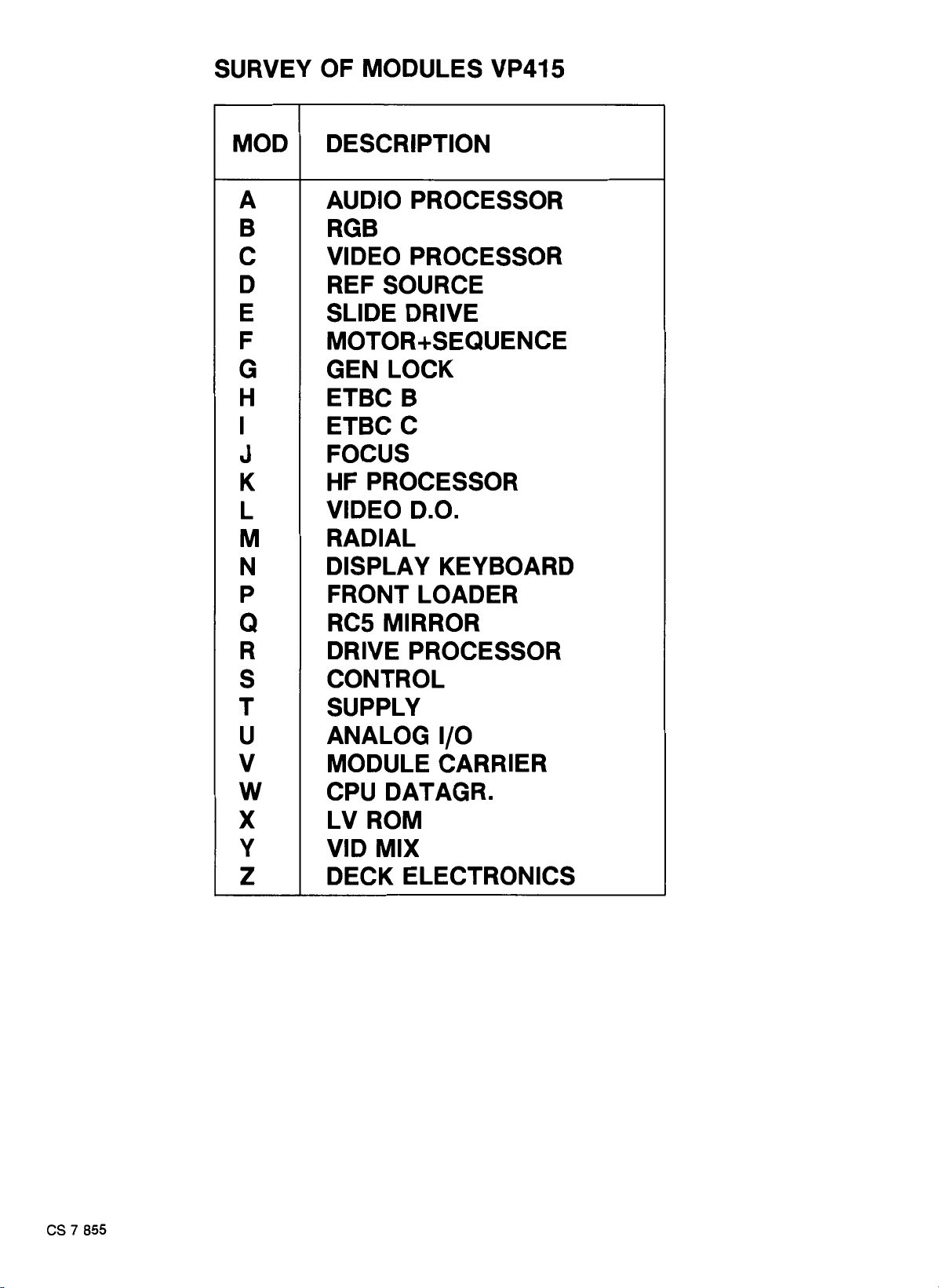
SURVEY OF MODULES VP415
MOD DESCRIPTION
A AUDIO PROCESSOR
B
C
D REF SOURCE
E SLIDE DRIVE
F
G
H
I
J
RGB
VIDEO PROCESSOR
MOTOR+SEQUENCE
GEN LOCK
ETBC B
ETBC C
FOCUS
K HF PROCESSOR
L
VIDEO D.O.
M RADIAL
N DISPLAY KEYBOARD
p
Q
R
s
FRONT LOADER
RCS
DRIVE PROCESSOR
CONTROL
MIRROR
T SUPPLY
u
ANALOG 1/0
V MODULE CARRIER
w CPU DATAGR.
X
y
z
LV
ROM
VID MIX
DECK ELECTRONICS
CS
7 855

=
=
-~
--
:
~
;j
.,
,.j
@(]
~
---
~J
~rJ
:---
...
MODULE CARRIER
tr,od level 1 )
[lJ
..
Ll
[lJ
ru·
-·
..
-·
[:l
LJ
0
0·
@]
--
ru
··
-·
.
.
ru
@]· ru@l·
--
-· -·
@]
.
.
Ll
·-
..:
El
i-j
i ::-l
:·-)
~~·-
~
. _ . _ 1
•• 1 .•...
···'
..
, . . . .• ,
'·"•
.••.
,,
...
,
,,
...
. . ,1 . . _.
·<!
...
:~
J~
i --:
l;J
D
El
i~
-· . .
~[§]
c::=J[,,J
[,,]:·,,,:
D
(fil
'
.,
, .
...
H
CS
7 836

.
AUDIO
PROC.
MODULE
(MOD LEVEL 2)
2004 B 6
2006 B 6
2007
A 3 2020 B 1 2034 A 2 2049 A 7 2066 A 3 2068 A 5 3003 A 1 3112 B 4 3114 A 4 5002 A 6
20
18 B 3
2021
A 7 2048 A 7 2065 A 3 2067 A 5 2069 A 2 3005 B 5 3113 A 4
2 3 4 5 6
5001
A 6 5003 A 6 5005 A 1 5007 A 7
5004
A 1 5006 A 1 5008 A 2 6002 A 7 6004 A 2 6107 B 1 6202 A 1
6001
B 6 6003 A 3
6102
8 5
6201
A 6 6203 A 4
ADJUSTMENTS
Required
Test
disc
Scope
Adjustment conditions
Load test disc
Normal play, picture no. 6200-6500 Audio
1,
6600-6900 Audio 2 (replay)
Audio modulation 1 kHz
Adjustments
1) R3003, R3005 (Audio demod)
- Measure the output voltage on
1A1
and
3A1
(AUD2 and
AUD1) with the scope.
- Adjust R3003 and R3005 until the output voltage is
1,8 Vpp.
Adjustment when item replaced:
replaced adjust
IC6201 R3005
IC6202 R3003
A
B
1001
B 3.
2010
1002
2001
2002 B 6 2013 B 6 2024 B 2
2003
2005
2008
2009
A
2011
B 3
B 6 2012 B 6 2023 B 2 2037
201
4
A 5
20
15
A 6
B 7 2016 B 1 2027 B 1
B 7
2017
2019 A 1
B 6
B 6
2022 B 2 2036 B 2 2053
B 6 2025
B 1
2026
A 1 2028 B 1
2
2030 B 6 2052
7
A
B 2
2039
B 1
2046 B 5
B 1 2047 B 1 2057 A 4
2050
2051
A 5
A 5
A 5
A 5
A 4
2054
A 4
2055
A 4 3001 B 6
2056
A 4
2058
A 5
2059
2 3
3
A 5 3007 B 6 · 3015 A 6 3023 B 6 3032
2060
2061
A 5
A 4
2062
A 4
2064
B 2
3002
B 5 3013 A 6
3004
A 6
3006
B 6 3016 A 7
3008
3009 B 5
10
A 5
30
11
A 6 3019
30
30
12
A 6
301
4 A 6
3017 B 2 3025 B 6
3018
3020
3021
3022 B 6
3024
B 7
3026
3027 B 2
B 6
B 6 3028
B 6 3030
303
4
B 1
B 6 3033
7
A
A 3 3037 A 1
A 1
1 B 1 3039 A 2 3047 B 1 3072 B 5
B 1
A 1
3034
A 2
3035
A 1 3044 B 2
3036
A 1
3038
A 2
3040
B 7
3041
3042 B 2
3043 B 2 3064
3045 B 2
B 1
3046
B 1 3073 B 1 3082 A 5
3048
B 1 3074
3049
A 5
3063
A 5 3077 A 2
A 5 3078 A 5
3065
A 5 3079 A 5 3087 A 5
3066
3071
B 5 3080
4
5 6
3090
3091
B 1 3083
3076 A
7
A 5
3081
A 5
5 6
A 5
A 4 3092
3084
A 4
3085
A 4
3086
A 4
3088
A 4 3097 A 4 6
3089
3093
3094
3095
3096
A 4
A 4
A 5
A 5 3108 B 2
A 5
A 5
A 4 3111
A 4 6103 A 6
3098
A 4 6104
3099
3107
B 7 6105 A 6 6118
3109 A 4 6108 A 1 6120
110
3
101
6106 B 1 6119 A 5
6109 A 1 6121 A 4
B 3
6110 A 2 6122 A 4
B 2
6115 A 5 6123 A 4
B 5
7
6116 A 5
A 6 6117 A 4
A 4
A 5
7
A
B
A
LIST OF ELECTRICAL PARTS MODULE A
Filters
5007
5008
4822 242 71658
4822 242 71659
SLC3251
SLC3252
Coils
009
009
008
008
8.mH
130 µH
130
µH
8mH
110 µH
110 µH
5001
4822 156 20928
5002 4822 156
5003
5004
5005
5006
4822 156
4822
156 20928
4822 156
4822 156
11
11
11
11
Potentiometers
3003
3005
4822 1 00
4822 1 00
11
087 2.2
11
087 2.2
kil
kil
2001
2002
2003
2004
2005
2006
2007
2008
2009
2010
2011
2012
2013
2014
2015
2016
2017
2018
2019
2020
2021
2022
B
2
4822 122 32808
1.2 nF
4822 122 32808 1.2 nF
4822 122 32856 8.2 nF
5322 124 21711
4822 122 32597
4822 124 22189
100 µF 25 V
6.8 nF
6.8 µF
63 V
5322 124 21749 10 µF 63 V
5322 122 32839 100 nF
4822 122 32442 10 nF
4822 122 31759 22 nF
4822 122 31768 180 pF
4822 122 32975
33 pF
4822 122 31759 22 nF
4822 122 32442 10 nF
4822 1 22 32808
1.2 nF
4822 122 32808 1.2 nF
4822 122 32856 8.2 nF
5322 124 21711
100 µF
25 V 2052 4822 122 31965
4822 122 32597 6.8 nF
4822 124 22189
5322 124 21749
5322 122 32839
6.8 µF 63 V 2054
10 µF
63 V 2055 4822 122 32442 10 nF
100 nF
4
5
2057
22 nF 2058
2023
2024
3
4822 122 32442 10 nF
4822 122 31759
2025 4822 122 32482 22 pF 2059
2026
2027 4822 122 31759
2028 4822 122 32442 10 nF
2030 4822 122 31759 22 nF
2034 5322 124 21711 100 µF 25 V
2036 4822 122 31759 22 nF
2037
4822 122 31766 120 pF
22 nF
2060
2061
2062
2064 4822 122 31783 2.7 nF
2065 5322 124 10512
2066 5322 124 21749
4822 122 33007 330 nF 25 V 2069 5322 124 21749
2039 4822 122 33007 330 nF 25 V
2046 4822 122 32927 220 nF
2047
2048
2049 5322 124 10512
2050 4822 122 32972
2051
4822 122 32927 220 nF
5322 124 21711 100 µF 25 V
68 µF 20% 16 V
nF
4822 122 31783
1
2.7 nF
220 pF
2053 4822 122 31774
56 pF
4822 122 31767 150 pF
2056 4822 122 31783 2.7 nF
6
5322 122 31647
4822 122 31783
4822 122 31965 220 pF
31
4822 122
774
4822 122 31767 150 pF
4822 122 32442 10 nF
7
PCB.00199
T10 718
1 nF
2.7 nF
56 pF
68 µF 20% 16 V
10 µF
10 µF 63 V
B
.,
63 V
 Loading...