

Page 1
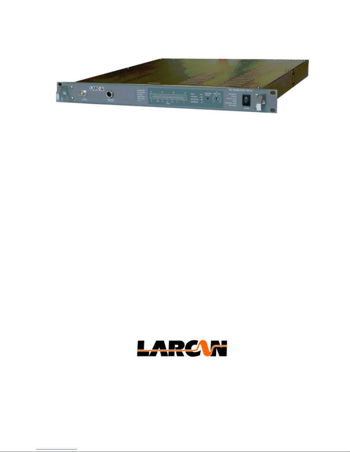
FMT- 25 VHF FM TRANSLATOR 862 -09725
FMT-25
VHF FM TRANSLATOR
TECHNICAL MANUAL
Issue 1A:
Page 2

FMT- 25 VHF FM TRANSLATOR 862 -09725
FMT-25
VHF FM TRANSLATOR
TECHNICAL MANUAL
CONTENTS:
1. Introduction
2. General Description
3. Technical Specifications
4. Operating Information
5. Installation Information
6. Technical Information
7. Maintenance information
Issue 1A:
Page 3

FMT- 25 VHF FM TRANSLATOR 862 -09725
INTRODUCTION
This Manual contains the Operating, technical and installation information for the FMT25 VHF FM Translator. The FMT-25 forms part of a new range of Professional VHF
FM Re-broadcasting equipment produced by Broadcast Solutions Electronics.
Issue 1A:
Page 4

FMT- 25 VHF FM TRANSLATOR 862 -09725
FMT-25
VHF FM TRANSLATOR
TECHNICAL MANUAL
General Description
Issue 1A:
Page 5

FMT- 25 VHF FM TRANSLATOR 862 -09725
GENERAL DESCRIPTION
The FMT- 25 VHF FM Translator is a compact unit requiring only 1U Rack space. The
unit is de signed for use in VHF FM Stereo Broadcasting in the 87.5MHz to 108MHz,
band. The unit will perform the function of a “Relay receiver” and “25W FM
Exciter”, providing Local (Display) and Remote (Telemetry) functions.
The FMT- 25 offers standard features that include:
• Automatic tuning of Rx Front -end filters.
• Fully synthesized in 50kHz steps (Tx and Rx).
• Rx Diversity operation capability.
• A/C and DC (+24V) operation.
ALC for RF Power control.
•
• Telemetry output.
• Rx Headphone output.
• RF Monitor output.
• Comprehensive metering and indicators.
The FMT- 25 offers a range of customer options that include:
• ID Module for internal SCA insertion.
The FMT- 25 provides a High quality, compact and versatile solution for VHF FM Re-
broadcasting and only requires 1U rack space.
The unit includes a fully synthesized FM Receiver with Front -end tracking filters
and a highly selective Ceramic IF Filter. A Tracking demodulator and 100kHz Low
pass filter are also standard features of the receiver section. The unit also inclu des a
fully synthesized FM Modulator with provision for internal and external Baseband
inputs. The FMT- 25 has a 25-Watt RF Power amplifier module with integral SMPSU.
Low pass RF Filter and couplers are standard on this module.
The FMT- 25 is equipped wi th a +24V dc input, which can be used for Battery/Solar-
powered operation or as back up for mains failure condition. The dc input is internally
fused for protection purposes. The rectified a/c input is also fused internally, while the
a/c mains input is fused on the rear panel.
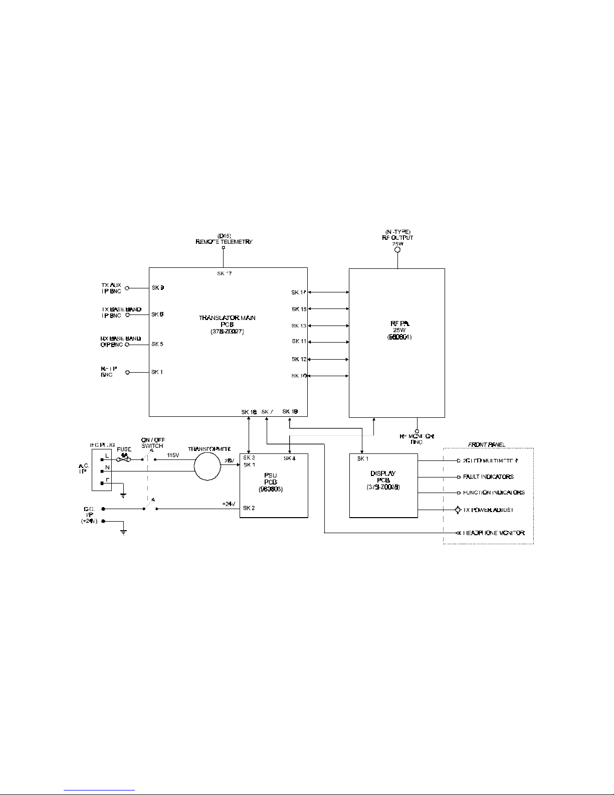
The schematic diagram of the FMT-25 is shown in figure 2 below.
3. STRUCTURE.
The FMT- 25 comprises of the following modules.
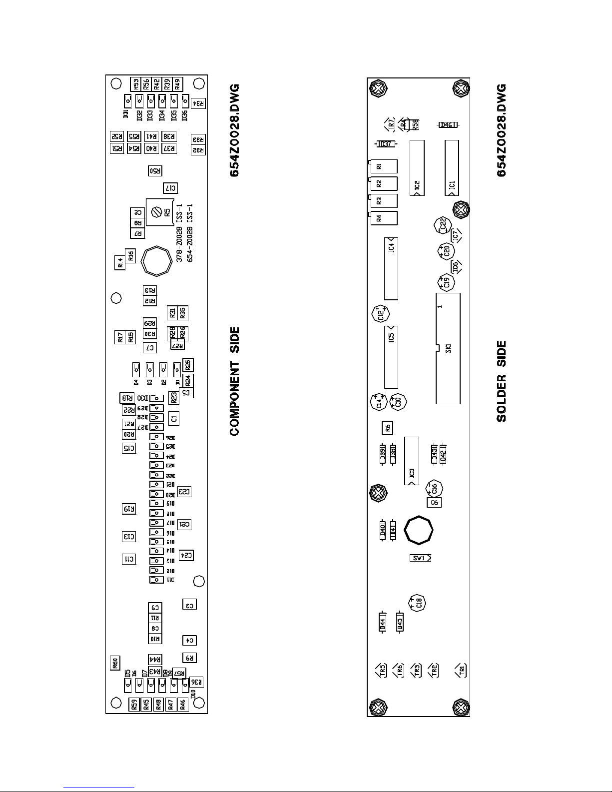
a) Display PCB (378-Z0028).
b) Main PCB (378-Z0027).
c) RF PA Module (980801).
Issue 1A:
Page 6

FMT- 25 VHF FM TRANSLATOR 862 -09725
d) PSU Module (980808).
Each module is Field replaceable, in line with BSE’s maintenance philosophy. This
allows the customer to change a module, or to upgrade options easily.
4. FUNCTIONAL DESCRIPTION.
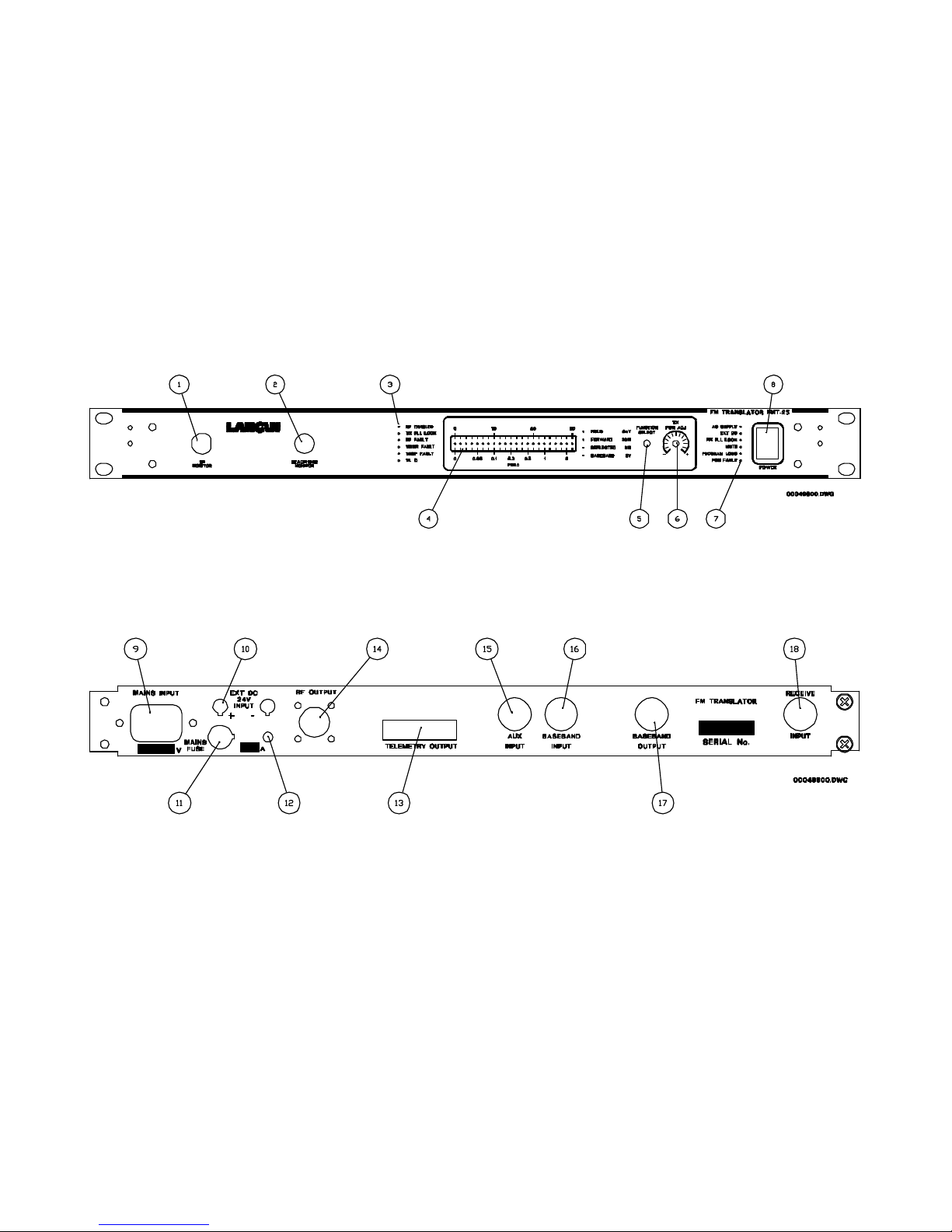
Refer to the Front and Rear panel layout in figure 1.
1) RF monitor (BNC 50 ohms female) .
2) Rx Headphone monitor (Stereo ¼ inch Jack socket).
3) Tx indicators and alarms.
4) Bargraph meter (20 dot) .
5) Bargraph meter function selector (Selects one of four metered parameters).
6) Tx Power adjustment (potentiometer) .
7) PSU / Rx indicators and alarms.
8) Powe r on/off switch: Switches a/c (Mains) and dc (+24V) supplies.
9) A/C Mains input Europlug (IEC) connector for a/c supply.
10) Ext. 24V dc input: Positive (+) and negative (-) dc binding terminals.
11) A/C Mains Fuse: Fuse (1Amp/230V or 2A/115V).
12) Ground: M5 Screw for chassis ground.
13) Telemetry: D15 (female) connector for remote commands and alarms.
14) RF Output (N Type 50 ohm female).
15) Tx Auxiliary baseband input (BNC female for SCA/SST Sub-carrier injection) .
16) Tx Baseband input (BNC female for composite/MPX injection).
17) Rx Baseband output (BNC female for Rx composite/MPX output).
18) Input Receiver (BNC 50 ohms female for received RF input).
Issue 1A:
Page 7
FMT- 25 VHF FM TRANSLATOR 862-09725
Issue 1A:
Figure 1: Front and Rear panel layout.
Page 8
FMT- 25 VHF FM TRANSLATOR 862-09725
Issue 1A:
Figure 2: Schematic Diagram of FMT-25
Page 9

FMT- 25 VHF FM TRANSLATOR 862-09725
FMT-25
VHF FM TRANSLATOR
TECHNICAL MANUAL
Technical Specifications
Issue 1A:
Page 10
FMT- 25 VHF FM TRANSLATOR 862-09725
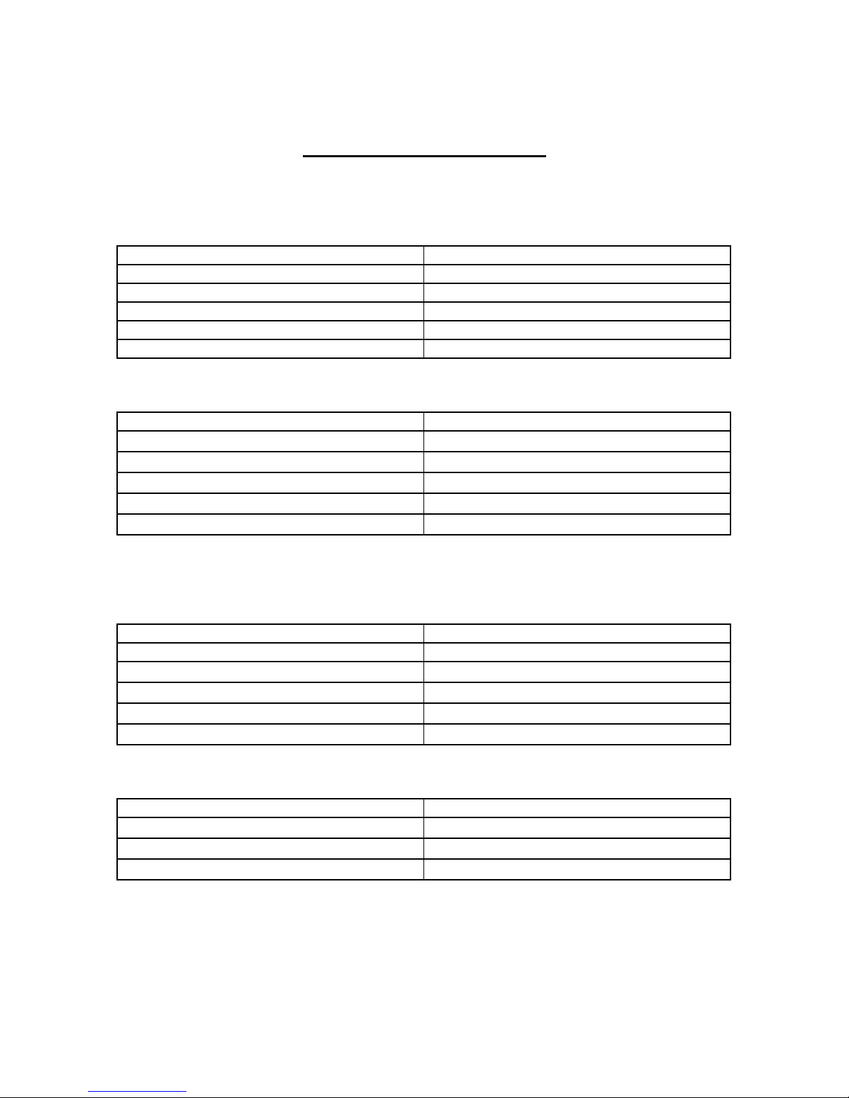
FMT- 25 SPECIFICATIONS
Electrical characteristics
Typical Rx Sensitivity: 75kHz-deviation reference with 75uS de-emphasis (Stereo)
RF Input level Stereo S/N ratio
20uV 50dB
50uV 56dB
100uV 60dB
500uV 70dB
1000uV 75dB
Rx Static selectivity: RF Filter, IF Filter and Rx baseband filter
Frequency offset Selectivity
± 100kHz
± 200kHz
± 300kHz
± 400kHz
± 500kHz
Rx Dynamic selectivity: 75kHz deviation reference and 75uS de-emphasis for 54dB
S/N ratio (Stereo).
Frequency offset Selectivity
0kHz -46dB
± 100kHz
± 200kHz
± 300kHz
± 400kHz
Rx baseband amplitude response:
Frequency Response
30Hz to 53kHz
53kHz to 95kHz
≥200kHz ≤ -65dB
0dB
-65dB
-90dB
-100dB
-110dB
-30dB
+6dB
+27dB
+35dB
± 0.1dB
± 1dB
Issue 1A:
Page 11

FMT- 25 VHF FM TRANSLATOR 862-09725
Rx baseband performance: Stereo with 75kHz deviation and de-emphasis off.
Tested at 1mV, RF input.
Frequency Distortion Separation Crosstalk
30Hz
1kHz
5kHz
15kHz
≤ 0.25% ≥ 50dB ≥ 50dB
≤ 0.25% ≥ 50dB ≥ 50dB
≤ 0.25% ≥ 50dB ≥ 50dB
≤ 0.25% ≥ 50dB ≥ 45dB
Tx baseband amplitude response: Input via Tx baseband input.
Frequency Response
1Hz - 3dB
30Hz to 53kHz
53kHz to 100kHz
± 0.1dB
± 0.25dB
Tx baseband performance: Stereo with 75kHz deviation.
Tested with FM Stereo demodulator and decoder.
Frequency Distortion Separation Crosstalk
30Hz
1kHz
5kHz
15kHz
≤ 0.15% ≥ 50dB ≥ 50dB
≤ 0.15% ≥ 50dB ≥ 50dB
≤ 0.25% ≥ 50dB ≥ 50dB
≤ 0.25% ≥ 50dB ≥ 50dB
General Tx/Rx specifications:
Tx/Rx Frequency range 87.5MHz to 108MHz
Tx/Rx Frequency separation
≥400kHz
Tx/Rx Frequency increments 50kHz steps (synthesized)
Tx/Rx Frequency stability
Tx RF Output power
Tx Harmonics and spurious
Tx out of lock attenuation
Tx AM Non synchronous
≥25W (Adjustable via front panel)
± 2ppm
≤ -60dBc
≥ 70dB
≤ -60dBc
Tx baseband i/p Z 10k ohms
Tx baseband i/p sensitivity 3.5V p-p for 75kHz peak deviation
Tx Aux. baseband i/p Z 10k ohms
Tx Aux. baseband i/p sensitivity 3.5V p-p for 3kHz peak deviation
Issue 1A:
Page 12

FMT- 25 VHF FM TRANSLATOR 862-09725
Environmental Specifications
A/C Input power
A/C Frequency variation 50Hz to 60Hz
DC Input power +24V Battery (+24V to +28V)
Power consumption Approximately 70W
Storage temperature
Operating temperature
Relative Humidity 20% to 90% non condensing
Operating Altitude
Cooling system Convection (Blower option)
Dimensions 480mm x 450mm x 44.4mm
Physical mass Approximately 7kg
Back Panel connectors and Functions.
Function Connector
RF output N Type Female (50 ohm)
Rx input BNC Female (50 ohms)
Rx baseband o/p BNC Female
Tx baseband i/p BNC Female
Tx Aux. baseband i/p BNC Female
Telemetry (input/output) D15 Female
Ext. dc Input (+24V Battery) 2 x Terminal posts
A/C Mains input IEC Europlug
A/C Fuse (1A/230V 2A/115V) 20mm Type
Chassis Ground 5mm screw Fixing
Front panel controls and indicators.
Control / indicator Function
RF Enabled led (green) Indicates Remote enable function
Tx PLL Lock led (green) Indicates Tx PLL is in Lock
RF Fault led (red) Indicates Forward power is low
VSWR Fault led (red) Indicates Reflected power is high
Temp Fault led (red) Indicates RF PA Temp is high
TL ID led (yellow) Indicates TL ID Module installed
A/C Supply led (green) Indicates A/C Supply is present
EXT DC led (green) Indicates +24V DC Supply is present
Rx PLL Lock led (green) Indicates Rx PLL is in Lock
Mute led (red) Indicates Rx is Muted
Program loss led (red) Indicates Loss of program
PSU Fault led (red) Indicates PSU Failure
Function select LED’s (yellow) Indicates meter function selected
Tx Power adjust potentiometer Sets required Tx RF Power
Headphone stereo monitor jack 600 ohm headphones for Rx program
RF M onitor BNC (50 ohm) Samples Tx output for test purposes
115V ± 10% (230V Optional)
-40°C to +60°C
-10°C to +45°C
≤2500m above sea level
Issue 1A:
Page 13

FMT- 25 VHF FM TRANSLATOR 862-09725
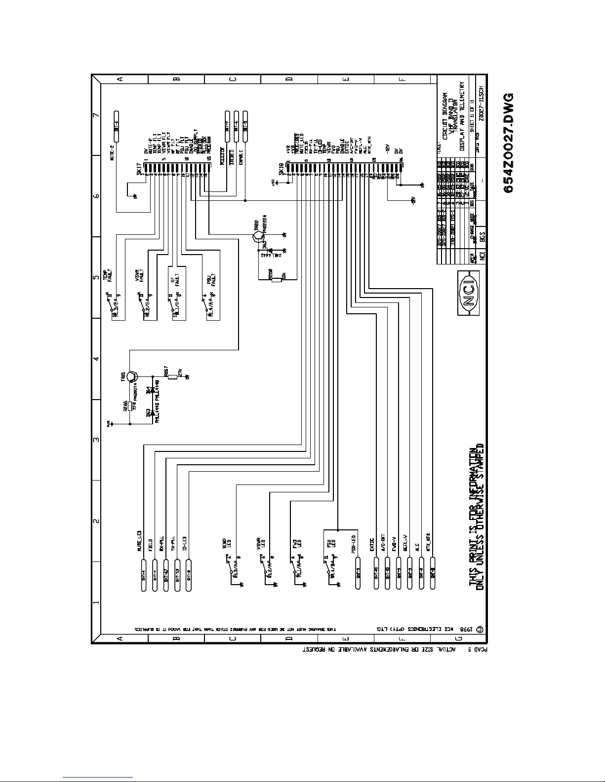
Telemetry controls and alarms (via 15-pin D type female connector).
Pin number on SK17 Description
Pin 1 OV
Ground
Pin 2 Rx Mute
(Contact s/c to ground when muted)
Pins 3 and 4 RF PA Temperature Fault
(Voltage free contact, s/c when fault)
Pins 5 and 6 RF PA VSWR Fault
(Voltage free contact, s/c when fault)
Pins 7 and 8 Low RF power Fault
(Voltage free contact, s/c when fault)
Pins 9 and 10 PSU Fault
(Voltage free contact, s/c when fault)
Pin 11 Tx Enable
S/c to Ground to disable
Pin 12 Jig supply
+22V at 20mA
Pin 13 Stereo indicator
npn open collector / ground for stereo
Pin14 PLL Lock indicator
npn open collector / ground for lock
Pin 15 14 sec. Program loss indicator
npn open collector / ground for program
Issue 1A:
Page 14

FMT- 25 VHF FM TRANSLATOR 862-09725
FMT-25
VHF FM TRANSLATOR
TECHNICAL MANUAL
Operating Information
Issue 1A:
Page 15

FMT- 25 VHF FM TRANSLATOR 862-09725
OPERATING INFORMATION
Translator Applications:
• Stand alone Translator: When used with VHF receive and Transmit antennas.
• High power Translator: When used with VHF receive and Transmit antennas and
Wideband VHF RF Amplifier.
• Translator with Space Diversity: When used with VHF receive and Transmit antennas
with a Reserve Receiver connected in Diversity mode.
Operating and interface information.
Refer to the Front and Rear panel layout in figure 1.
RF monitor
1)
Rx Headphone monitor
2)
Tx indicators and alarms.
3)
Bargraph meter
4)
Bargraph meter function selector
5)
Tx Power adjustment
6)
PSU / Rx indicators and alarms.
7)
Power on/off switch
8)
A/C Mains input
9)
Ext. 24V dc input
10)
A/C Mains Fuse
11)
Ground:
12)
Telemetry
13)
RF Output
14)
Tx Auxiliary baseband input
15)
Tx Baseband input
16)
Rx Baseband output
17)
Input Receiver
18)
(BNC 50 ohms female).
(Stereo ¼ inch Jack socket).
(20 dot).
(Selects one of four metered parameters).
(potentiometer).
: Switches a/c (Mains) and dc (+24V) supplies.
Europlug (IEC) connector for a/c supply.
: Positive (+) and negative (-) dc binding terminals.
: Fuse (1Amp/230V or 2A/115V).
M5 Screw for chassis ground.
: D15 (female) connector for
(N Type 50 ohm female).
(BNC female for SCA/SST Sub-carrier injection).
(BNC female for composite/MPX injection).
(BNC female for Rx composite/MPX output).
(BNC 50 ohms female for received RF input).
remote
commands and alarms.
Metered parameters
• Field strength: 3mV full scale (bottom scale).
• Forward RF Power level: 30W full scale (top scale).
• Reflected RF Power level: 3W full scale (top scale).
• Baseband level: 3V-rms full scale (top scale).
To adjust RF output power, select “Forward” on function select switch and adjust TX
PWR ADJ control to set desired RF output power.
Issue 1A:
Page 16

FMT- 25 VHF FM TRANSLATOR 862-09725
Indicating LED’s:
• A/C Supply: Green led indicates A/C power is On.
• EXT DC: Green led indicates +24V ext. DC power is On.
• Rx PLL Lock: Green led indicates PLL lock is achieved.
• Mute: Red led indicates Rx is muted.
• Program Loss: Red led indicates loss of Rx program/modulation.
• PSU Fault: Red led indicates psu failure.
• RF Enabled: Green led indicates RF is enabled.
• Tx PLL Lock: Green led indicates PLL lock is achieved.
• RF Fault: Red led indicates low RF output.
• VSWR Fault: Red led indicates high-reflected power.
• Temp Fault: Red led indicates high temperature in RF PA module.
• TL ID: Yellow led indicates ID module is connected.
Rear panel
(a) A/C Input: IEC male connector for prescribed a/c operation. (7)
(b) A/C Fuse: Accepts 1 Amp 20mm type fuse. (9)
(c) DC Input: Red/Black terminal posts for +24V Battery operation. (8)
(d) Ground post: 5mm screw for grounding purposes.
(e) Telemetry: 15 pin D type (female) for remote control/monitoring. (11)
(f) De-emphasis: Switch to enable stereo decoder de-emphasis. (10)
(g) Diversity input: BNC input for Wideband/MPX reserve. (12)
(h) Baseband outputs: BNC outputs for re-broadcast purposes. (12)
(i) Remote PLL: 15 pin D type (female) to set remote frequency. (14)
(j) R F Input: N Type 50 ohm (female) for RF input. (15)
Frequency Selection
The operating frequency will normally be set at factory configuration, but if a different operating (
receive or transit) frequency is necessary then the unit top cover has to be removed and a new
frequency selected on the Translator main PCB
(378-Z0027)
. This is done by setting the DIL
switches as detailed in Table 3 in the Installation Section of this manual.
Issue 1A:
Page 17

FMT- 25 VHF FM TRANSLATOR 862-09725
FMT-25
VHF FM TRANSLATOR
TECHNICAL MANUAL
Installation Information
Issue 1A:
Page 18

FMT- 25 VHF FM TRANSLATOR 862-09725
INSTALLATION
INSTALLATION
STAND ALONE CONFIGURATION (FM Translator)
The following information sets out the general requirements for installation and operation of
the above equipment in a "stand alone" configuration.
Note: The operating frequency will normally be set at factory configuration, but if a different
operating ( receive or transit) frequency is necessary then the unit top cover has to be
removed and a new frequency selected on the Translator main PCB
(378-Z0027)
. This is done
by setting the DIL switches as detailed in Table 3.
1.
ELECTRICAL CONNECTIONS
Ensure that the power on/off switch on the front panel is switched off before proceeding.
a) A/C MAINS SUPPLY (115V 50Hz).
Connect a/c power cable to IEC connector on back panel.
b) DC SUPPLY (+24V dc).
Connect dc power input to the dc supply terminals on the back panel observing correct
polarity.
c) RF OUTPUT.
Connect the Antenna cable to the RF Output on the back panel using an N type connector
or via suitable adapters.
d) RF INPUT.
Connect RF input to BNC input, Input Receiver, on the back panel.
Note: When the Telemetry connector is not in use the unit requires no external commands to
enable the RF.
2. OPERATION
With the electrical connections completed above the unit is now ready for operation.
a) SWITCH ON SEQUENCE
Adjust the RF power control on the front panel, fully acw. then set the power on/off
switch to ON.
b) FRONT PANEL LED's:
RF ENABLE (green led) ON
Issue 1A:
Page 19

FMT- 25 VHF FM TRANSLATOR 862-09725
TX PLL LOCK (green led) ON
RF FAULT (red led) ON
VSWR FAULT (red led) OFF
TEMP FAULT (red led) OFF
TL ID (yellow Led) OFF
AC SUPPLY (green led) ON
EXT DC (green led) ON
RX PLL LOCK (green led) ON
MUTE (red led) OFF
PROGRAM LOSS (red led) OFF
PSU FAULT (red led) OFF
c) ALC METER (not fitted on this unit).
d) MULTIMETER
Select the four functions in turn and check the meter readings:
•
FIELD Indication of received RF level.
•
FORWARD POWER 0 Watts (no Leds on).
•
REFLECTED POWER 0 Watts (no Leds on).
•
BASEBAND Indication of received RF level.
e)
SETTING THE RF POWER LEVEL
Select FWD POWER on the Multimeter and observe the reading.
Adjust the Front panel TX PWR ADJ potentiometer clockwise to set the RF output power to
25W. (This should be achieved with 16 Leds on).
Now check the PA CURRENT and REFL POWER readings:
PA CURRENT should be approximately 1.9 Amps.
REFL POWER should be less than 2.5W (16 Leds).
Check all the fault Leds on the front panel and ensure that there are no
red Leds
on .
The unit is now operational and only the final temperature must be monitored after
approximately 15 minutes. The temperature reading on the front panel Multimeter should
settle down to approximately 12°C above Room temperature.
MECHANICAL
The unit is designed to fit in a standard 19 inch rack, cabinet structure. There is a Slide rail kit
(option) available for this purpose which allows the unit to be installed in this manner.
Due to the weight of the unit it is not recommended to mount the unit without proper
support.
INTERCONNECTIONS
Issue 1A:
Page 20

FMT- 25 VHF FM TRANSLATOR 862-09725
The external cables and connectors are not normally supplied as standard kit, and due
to the various customer configurations the cable and connector requirements must be
requested by the customer
.
Issue 1A:
Page 21

FMT- 25 VHF FM TRANSLATOR 862-09725
FMT-25
VHF FM TRANSLATOR
TECHNICAL MANUAL
Technical Information
Issue 1A:
Page 22

FMT- 25 VHF FM TRANSLATOR 862-09725
TECHNICAL INFORMATION
CIRCUIT DESCRIPTIONS
v
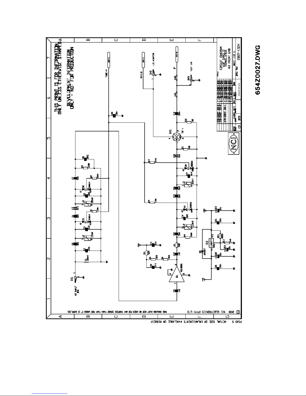
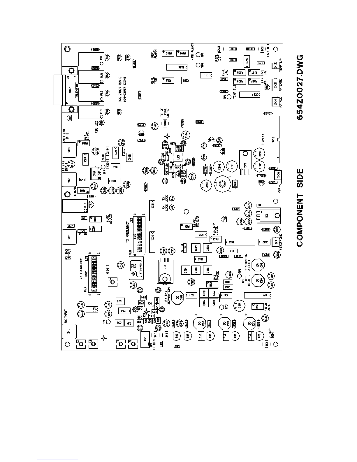
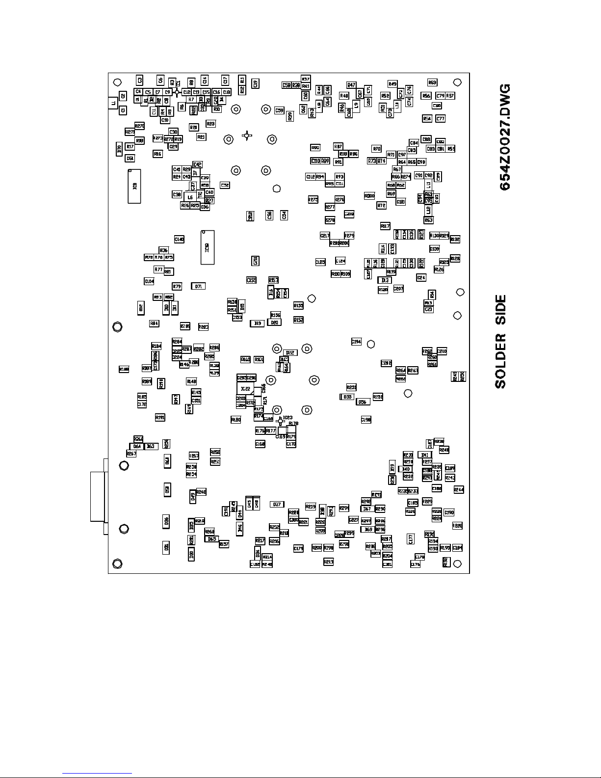
MAIN PCB ASSEMBLY (378-Z0027)
♦ Receiver Circuits operation.
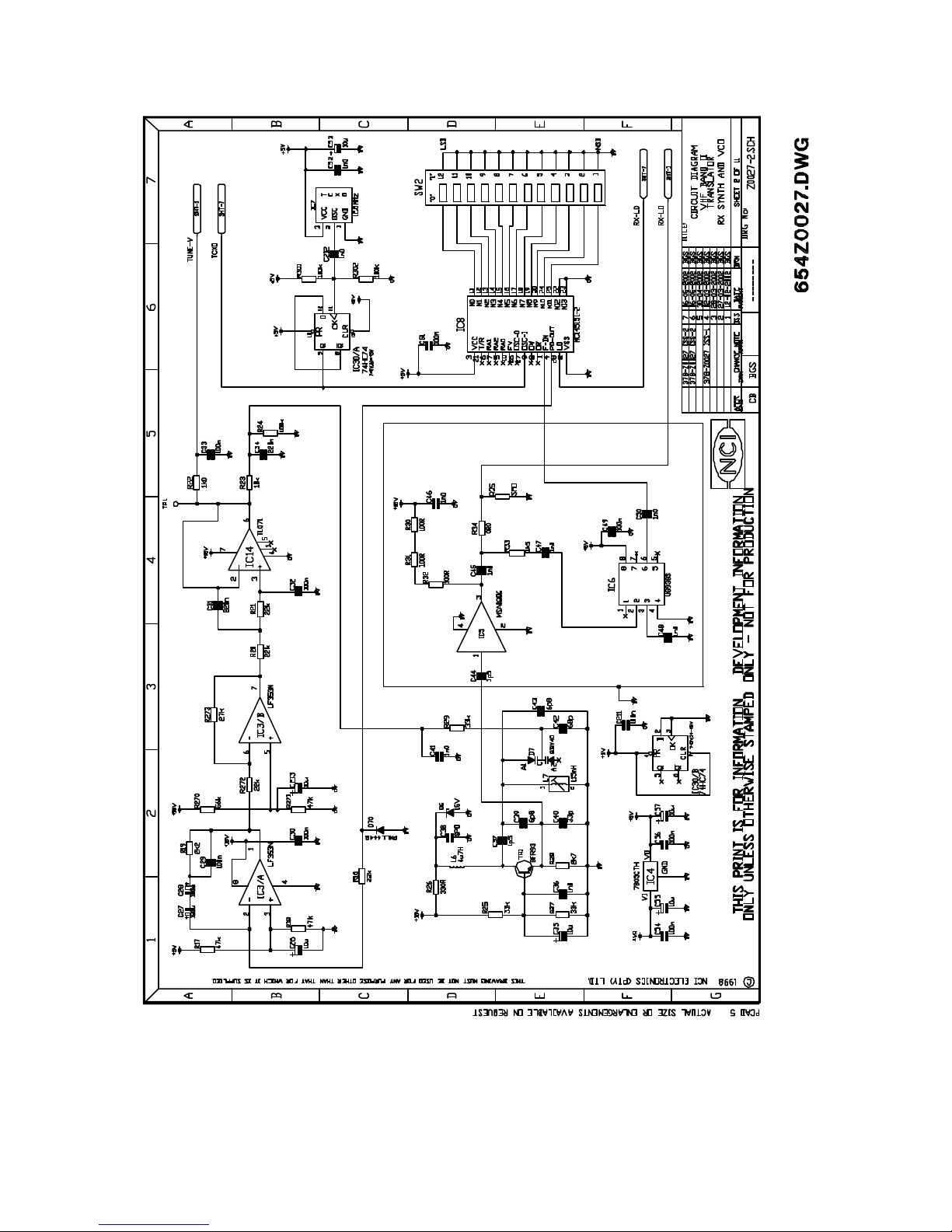
Synthesizer and Local Oscillator (76.8MHz-97.3MHz)
The synthesizer consists of a single modulus loop with a divide by 64 pre-scaler (IC6). A
12.8MHz TCXO (IC7) provides an accurate and stable reference for the synthesizer. The
reference is then, divided by two by IC30/A to 6.4MHz. This reference is applied direct to
the fixed divider in the synthesizer (IC8). This divides by 8192 to obtain a comparison
frequency of 781.25Hz. This mode of operation provides frequency steps of 50kHz via
the 12 way DIP switch SW2. (64 x 781.25Hz = 50kHz).
The LD output on IC8 provides a lock detect function and is routed to IC21/C for Telemetry
and Metering purposes. LED D18 provides the Rx Lock function indication.
The Local oscillator (TR1 and Buffer/amplifier IC5) is routed via the pre-scaler (IC6) to the
programmable divider in the synthesizer (IC8), whose division ratio is set by DIP switch
(SW2). The DIP switches set the L.O. Frequency (76.8MHz-97.3MHz), which is 10.7MHz
lower than the required receive frequency (87.5MHz-108MHz).
The P hase comparator output of IC8 (PD-OUT) has a 3-state output and is applied to a
Loop integrator (IC3) and Loop filter (IC14), whose dc output in turn, controls the
frequency of the Local oscillator via Varactor diode D7. (Control sensitivity is
approximately 2MHz/Volt).
The Local oscillator output can be monitored via SK2.
Front End Filters and Amplifier.
The Front End Filter is Self-Tuning and is configured into two sections, pre and post
amplifier. The RF input is routed from SK1 to the First filter stage (L2 and L3). The
amplifier (IC1) is configured to accept high overload levels with a gain of 30dB and low
Noise Figure of 3dB. This is done to ensure high sensitivity and low intermodulation
products.
The pre-amplifier filter consists of a seventh order bandpass, which is tuned via Varactor
diodes D1, and D2 and inductors L2 and L3. The Tuning voltage is derived from the L.O.
Locking voltage at IC14.
The output of IC1 is applied via a fixed attenuator to the Post-Amplifier filter stage (L4 and
L5) which is identical to the above filter.
This attenuator is used to provide a good match (50 ohms) to the filter and amplifier while
limiting the input level to the Mixer (MX1). The mixer is a passive double balanced type
with a Local oscillator drive level of +7dBm from IC5.
The overall performance of the Front End is typically 15dB, conversion gain with a noise
figure of 5dB. Image rejection is better than 65db across the entire band without any
tuning.
Issue 1A:
Page 23

FMT- 25 VHF FM TRANSLATOR 862-09725
10.7MHz IF Filter section.
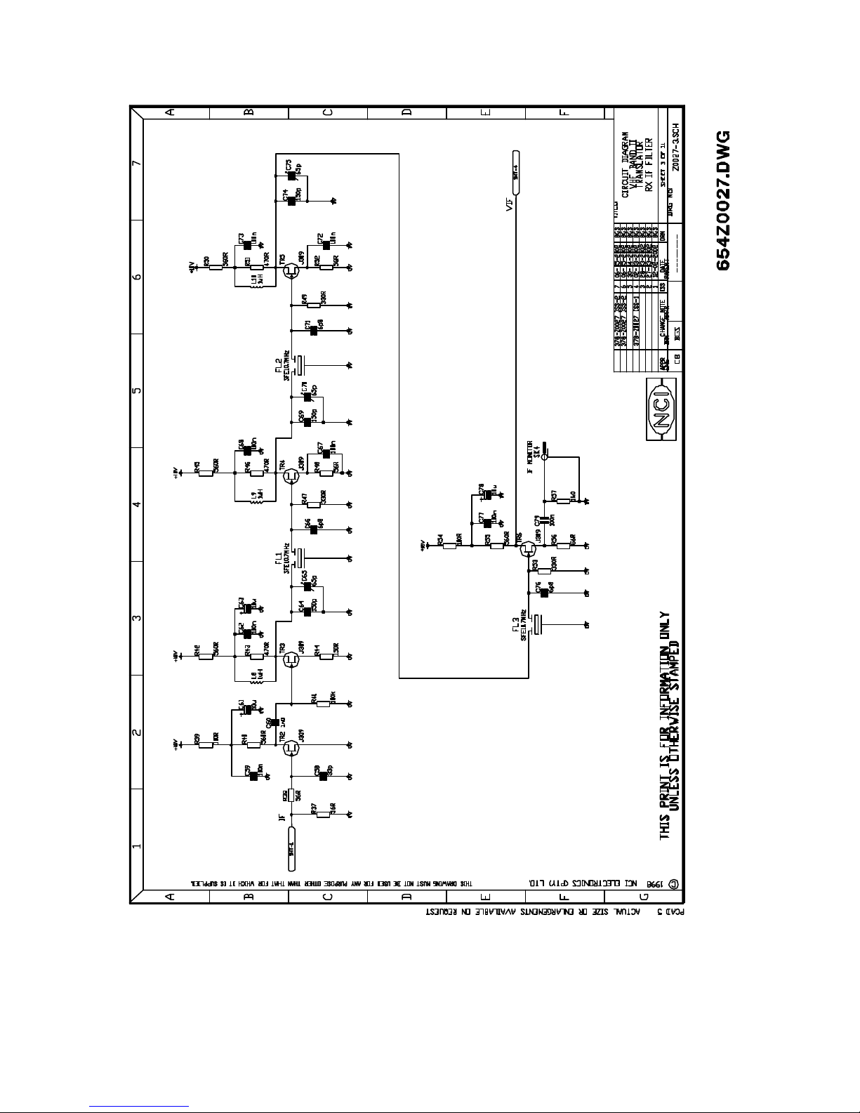
The 10.7MHz IF output from the Mixer MX1, is routed via Links LK1 and LK2 which are
usefully configured to allow testing of the Rx Front-end or IF Filter.
With LK1 ‘in’ and LK2 ‘out’ the Front-end IF output can be monitored at SK3.
With LK1 ‘out’ and LK2 ‘in’ the IF Filter can be tested separately via SK3/SK4.
LK1 and LK2 must both be inserted at final test.
The 10.7MHz filter consists of three Ceramic filters (FL1, FL2 and FL3), that have
controlled group delay and excellent attenuation characteristics. Each filter has tuning
capacitors at the input side (C65, C70 and C75) to obtain optimum Baseband distortion
and Stereo characteristics. Each filter is buffered by a J-Fet high impedance amplification
stage to recover the insertion loss of the individual filters (approximately 8db). The filters
are terminated with optimum, 330 ohms resistive loads. The complete filter gives
attenuation of approximately 20dB at 200khz offset and 60dB at 300khz offset. Spurious
response is better than 75dB.
The High Q of the ceramic filters ensure excellent performance and stability
compared to normal LC Filters.
IF Demodulator (10.7MHz).
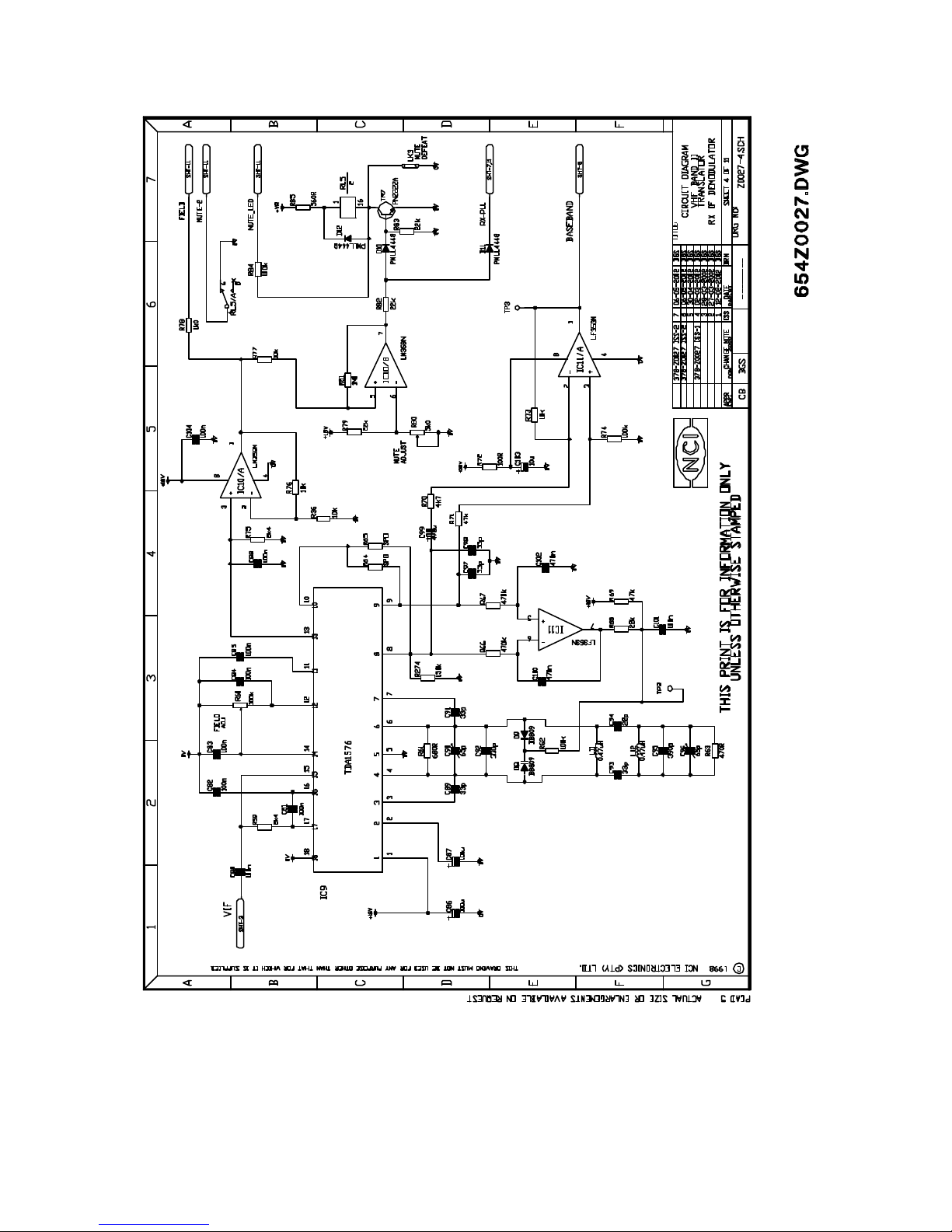
The IF demodulator consists of a double tuned, self correcting quadrature
demodulator (IC9). This is done to ensure optimum performance with temperature,
aging and input frequency offset error.
The balanced output of the demodulator at pins 8 and 9 contain the recovered
baseband and also a differential dc offset proportional to the 10.7MHz RF input
frequency offset. This dc offset is applied to IC11/B , which amplifies the dc offset and
applies it to Varactor diodes D8 and D9, which in turn tune the demodulator. This
corrects the error and ensures the distortion is minimized. C90 and C96 are provided
to initially optimally tune the demodulator.
A dc voltage proportional to the Field strength is provided on pin 13 of IC9 which is
applied to buffer IC10/A whose output is applied to IC10/B which is used to set the Rx
Mute level via R80. The output from IC10/A is also routed to SK18 pin 5 for Field strength
metering purposes.
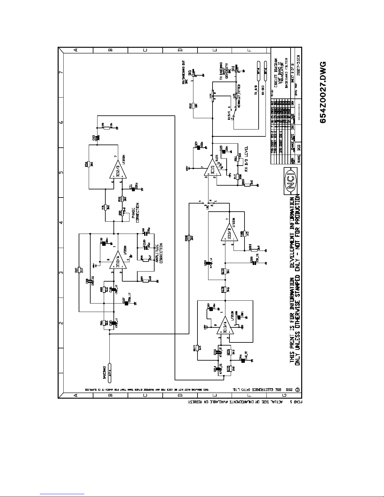
Baseband correction.
The Baseband output of the demodulator is amplified by IC11/A and applied to the
amplitude correction circuit at IC12/A. This circuit is used to correct the Roll-off of the
IF Filter and correct the amplitude response to 100kHz (adj. C109). The circuit also
acts as a band-reject filter attenuating frequencies at 200kHz by approximately 30dB. A
group delay correction circuit, IC12/B is also provided for optimal Stereo separation at
15kHz (adj. R92).
The performance of the complete IF demodulator is excellent, providing superb Stereo
separation and distortion at full 75kHz deviation of the 10.7MHz RF input, with ≥75db S/N
at only 1mV RF input level.
Rx Baseband Filter and output distribution.
The Baseband output signal on IC12/B pin 7 is applied to a 100kHz low pass filter
(IC13). This filter consists of a band reject at 150kHz (IC13/A) and a two- pole section at
Issue 1A:
Page 24

FMT- 25 VHF FM TRANSLATOR 862-09725
100kHz (IC13/B). The total filter is flat (± 0.25dB) to 95kHz and gives ≥20dB attenuation at
150kHz. No adjustment of the filter is necessary.
The baseband output from buffer IC15 pin 6 is routed via R112 to SK5 (Rx baseband
output) this output, whose level is adjustable via R111, is used for external use. The
output is also routed to LK4/A, which allows connection to RL5/B for internal loopback
purposes to the Tx modulator. When internal loopback is used LK5 can be inserted and
SK6 (Tx baseband input/diversity) can be used for ’standby’ receiver baseband input.
LK4/B can be used to switch the outputs for different switching configurations.
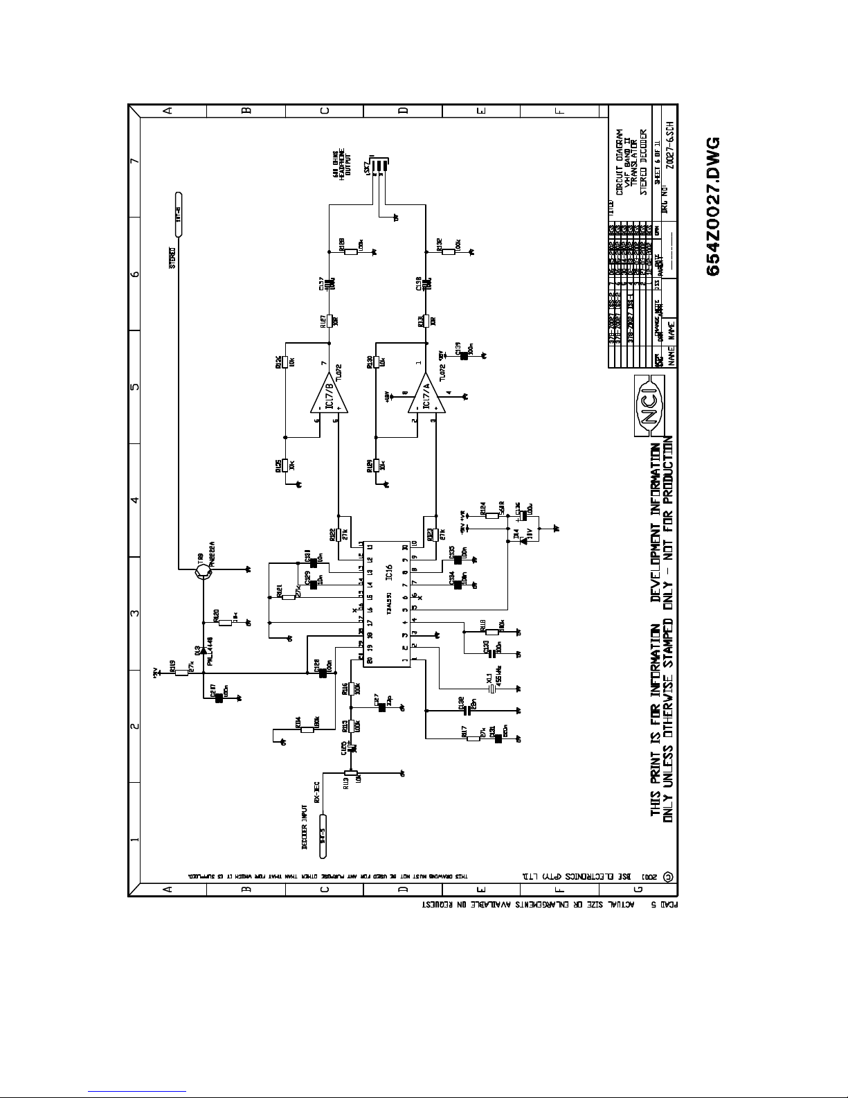
Stereo Decoder circuit. (Audio monitor and Pilot detection).
The output from IC15 is routed via R113 (Decoder level adjust), which sets the optimal
input level to IC16 (Stereo decoder). The S tereo decoder chip provides some interesting
internal features such as Image low pass filtering on input at 114kHz (3x38kHz),
Ceramic resonator (XL1) tuning (no adjustment of oscillators), Pilot detection with
pilot cancel circuit.
The stereo pilot signal, when present at the input, forces pin 18 ‘high’ via R119 which in
turn switches on TR8 and provides a Telemetry signal for external use on SK17 pin 13.
The Audio outputs are provided at pin 11 (Right) and pin 10 (Left) on IC16. The
outputs are de-emphasized via C129 and C130 and are routed to stereo headphone
buffers IC17/A and IC17/B . the outputs are routed to SK7 (Headphone output).
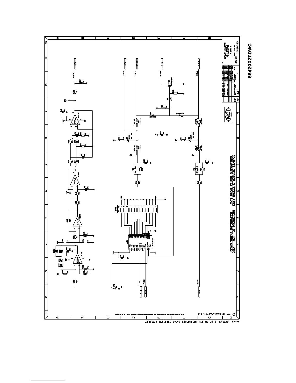
♦ Transmitter Circuits operation.
Synthesizer and modulator (87.5MHz-108MHz)
The synthesizer consists of a single modulus loop with a divide by 64 pre-scaler (IC6). A
12.8MHz TCXO (IC7) provides an accurate and stable reference for the synthesizer. The
reference is then, divided by two by IC30/A to 6.4MHz. This reference is applied direct to
the fixed divider in the synthesizer (IC18). This divides by 8192 to obtain a comparison
frequency of 781.25Hz. This mode of operation provides frequency steps of 50kHz via
the 12 way DIP switch SW3. (64 x 781.25Hz = 50kHz).
The LD output on IC18 provides a lock detect function and is routed to IC21/A for
Telemetry and Metering purposes. LED D17 provides the Tx Lock function indication.
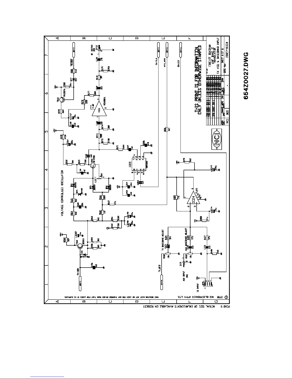
The modulator/oscillator (TR11 and Buffer/amplifier IC23) is routed via the pre-scaler
(IC22) to the programmable divider in the synthesizer (IC18), whose division ratio is set by
DIP switch (SW3). The DIP switches set the Oscillator Frequency (87.5MHz-108MHz).
The Phase comparator output of IC18 (PD-OUT) has a 3-state output and is applied to a
Loop integrator (IC19) and Loop filter (IC20), whose dc output in turn, controls the
frequency of the oscillator via Varactor diodes D23 and D24. (Control sensitivity is
approximately 2MHz/Volt).
Diodes D25 and D26 provide the modulation function and the dc control voltage tuning the
oscillator is also applied to these diodes. This dc voltage is offset via R160 and R161,
which equalizes the deviation level across the 87.5MHz to 108MHz band.
The Loop filter provides ≥40dB of attenuation at frequencies greater than 30Hz. This is
done to ensure that the Stereo m odulation, phase and amplitude are uninfected by the
Synthesizer loop to provide excellent stereo separation, even at 30Hz. The modulation is
inserted via IC24 and R167. SK6, SK8 and SK9 provide the input to the modulator.
Issue 1A:
Page 25

FMT- 25 VHF FM TRANSLATOR 862-09725
R182 provides the adjustment for the Tx baseband input, and R183 provides the Auxiliary
input (SCA or SST).
The RF output at SK10 and the RF Buffer amplifier (IC23) is switched via TR12 to
ensure the output is switched off when the synthesizer is out of lock.
Control, and RF detection.
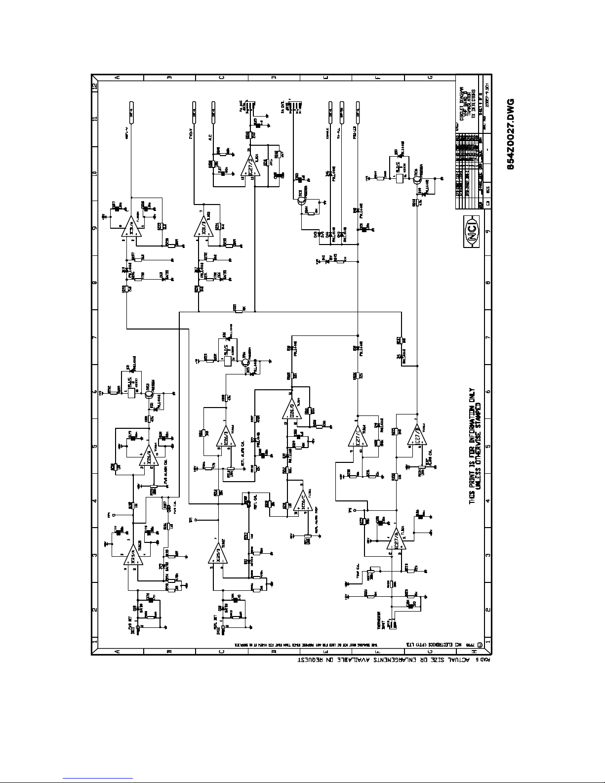
Forward power circuit:
The Forward power sample from the RF Power amplifier is input at SK11 and this RF
signal is converted to a dc level via diode D28 and amplifier IC25/A. Diode D29 is provided
to give temperature compensation for diode D28. The dc output at TP4 is normally set to
+5V dc via R197 (FWD cal) for 25W RF output in the RF Power amp module.
The output of IC25/A is routed to comparator IC26/A, which controls the alarm condition for
a Low RF Fault set by R199 (FWD Alarm cal). The output is then routed to TR13 and
RL1/C to provide contacts for Telemetry and Alarm indications.
Reflected power circuit:
The Reflected power sample from the RF Power amplifier is input at SK12 and this RF
signal is converted to a dc level via diode D32 and amplifier IC25/B. Diode D33 is provided
to give temperature compensation for diode D32. The dc output at TP5 is normally set to
+5V dc via R208 (REFL cal) for 2.5W RF reflected output in the RF Power amp module.
The output of IC25/B is routed to comparator IC26/B, which controls the alarm condition
for a High Reflected RF Fault set, by R215 (REFL Alarm cal). The output is then routed to
TR14 and RL2/C to provide contacts for Telemetry and Alarm indications.
The output from IC25/B is also routed to comparator IC26/C that sets the Reflected Trip
level via R211 (REFL Alarm trip). When activated the output is routed to IC26/D , which
performs the function of the timer. The timer allows the Reflected power re-cycle and
activation approximately every 14 Seconds.
Diode D34 allows the Reflected RF Fault to be latched during re-cycle periods during
which the Forward power is zero.
Temperature detection circuit:
The Thermistor in the RF Power amplifier is input at SK13. The resistance of the
Thermistor (4700 ohms at 25°C) reduces as the temperature increases and a dc output is
obtained at IC27/A pin 1 representing the actual temperature. The output voltage at TP6 is
set to actual temperature divided by 10 via R227 (Temp cal).
The output is then routed to comparator IC27/C (Temp trip) whose reference is set to
+6.5V. This allows the output of this IC to switch at a temperature of 65°°C, which in turn
switches off TR15 via D39 and this allows the command to the RF Power amplifier to be
switched off via SK15.
The output is also routed to comparator IC27/B (Temp fault) whose reference is adjustable
via R234 (Temp alarm cal). The output is routed to TR16 and RL3/C for Telemetry and
alarm purposes.
ALC Circuit:
The output dc from IC25/A (Forward detect voltage) is routed to via R239 to IC27/D. This
voltage is compared to the dc voltage on the ALC input (RF Power set) which is derived
Issue 1A:
Page 26

FMT- 25 VHF FM TRANSLATOR 862-09725
from the Display module. The output of this IC is routed via R243 to SK14 (PA ALC) and is
used to control the RF output on the RF Power amplifier module.
The output of the Temperature alarm circuit IC27/B is also routed to the ALC circuit via
R237 such that when the Temperature alarm is activated it reduces the RF output power.
Forward and Reflected meter correction.
The circuits of IC31/A and IC31/B are used to correct the non-linear dc detection voltages
(which are proportional to power) to linear voltages useful for driving a linear scale meter.
v
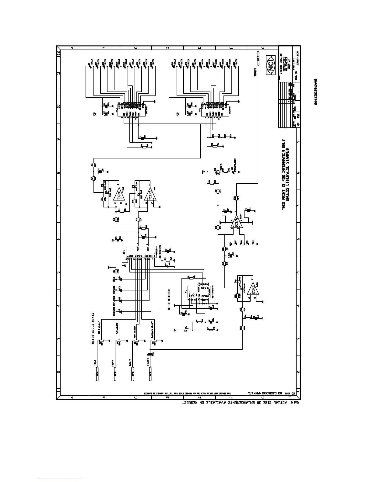
FMT DISPLAY PCB (378-Z0028)
Multimeter display.
The display consists of a 20 Led matrix driven by IC4 and IC5 (Linear Bargraph drivers).
The dc signal input to the Bargraph drivers is on pin 5. A push button selection switch
SW1 is provided to enable operation/selection. 1C1 provides the selection function while
IC2 provides switching and indication function. LED’s D1 to D4 are provided to indicate
parameter selected .
The display has 4 functions:
Parameter Adjust/calibrate Switch selection
Field strength R1 Position 1
Forward power R2 Position 2
Reflected power R3 Position 3
Baseband level R4 Position 4
The Field, Forward and Reflected signals are dc voltages whilst the Baseband signal is a
dynamic a/c signal (These inputs are on SK1). The signals are routed via IC2 to a full
wave, peak detection circuit (IC3/C and IC3/D) which has a fast attack time and slow
decay time to enable visual operation of the dynamic signal. This output is routed to
the Bargraph driver input on IC4 and IC5.
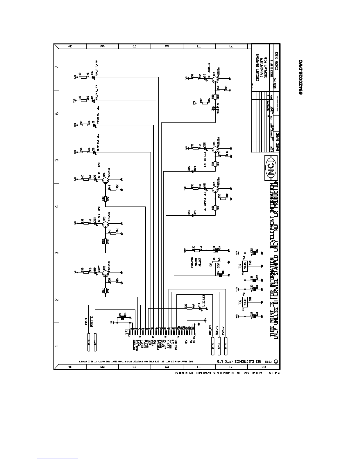
Program loss detector.
The incoming Baseband signal on SK1 pin 19 is routed to 1C3/B , which is a Half wave
peak detector circuit with fast attack and slow decay time. This circuit gives a dc output
proportional to the peak a/c input and capacitor C17 maintains the dc charge during
program durations. The circuit of IC3/A detects the dc output of the peak detector and
enables an alarm when it is low via SK1 pin 3 and TR1/LED D35. The program loss
condition takes approximately 12 seconds to register and is indicated by Led D35. The
filter R23, R24, R25 and C5, ensure that the stereo pilot signal does not activate the
program loss detector circuit.
Indicators and alarms (via SK1 inputs)
TX PLL Lock is indicated by Led D6 and is on when Lock condition exists.
RX PLL Lock is indicated by Led D33 and is on when Lock condition exists.
Mute is indicated by Led D34 and is on when Mute condition occurs.
Issue 1A:
Page 27

FMT- 25 VHF FM TRANSLATOR 862-09725
RF Enabled is indicated by Led D5 and is on when Tx is enabled.
Temp fault is indicated by Led D9 and is on when temperature is high.
PSU fault is indicated by Led D36 and is on when power supply is faulty.
RF fault is indicated by Led D7 and is on when RF power is low.
VSWR fault is indicated by Led D8 and is on when RF Reflected power is high.
A/C Supply is indicated by LED D31 and is on when A/C supply is present.
EXT DC is indicated by LED D32 and is on when dc supply (+24V) is present.
TL-ID is indicated by LED D10 and is on when ID Module is installed.
Front panel adjustments.
R5 adjusts the level of the Forward power via SK1.
Power supply.
The incoming power supply voltages are +22V (SK1 pin1 and 2), and –12V (SK1 pin
23). IC6 regulates the +12V supply and IC7 regulates the +5V supply.
v
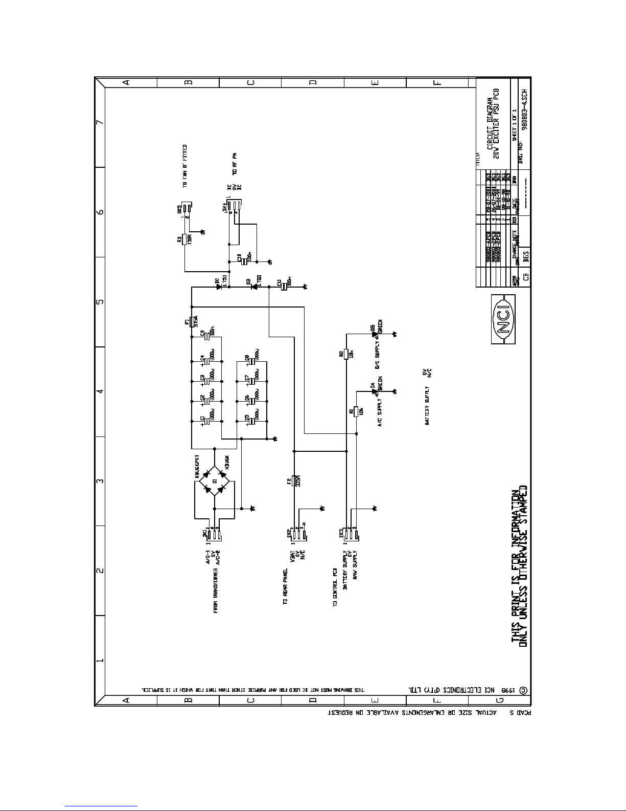
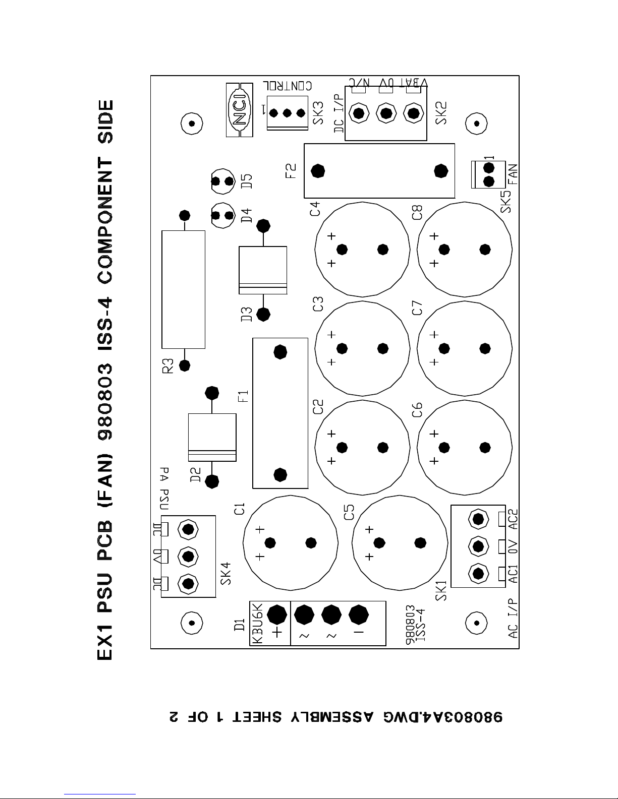
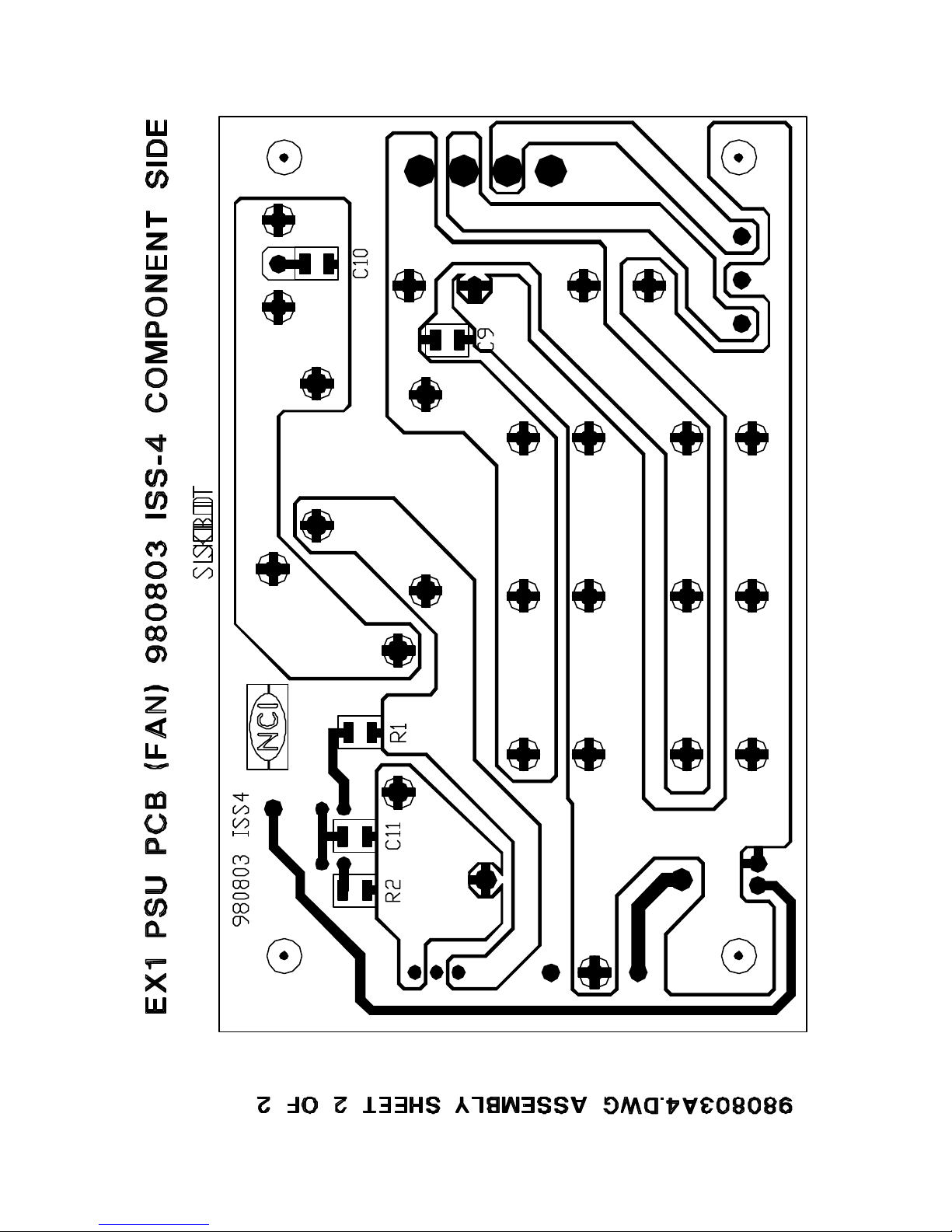
FMT POWER SUPPLY PCB (980808)
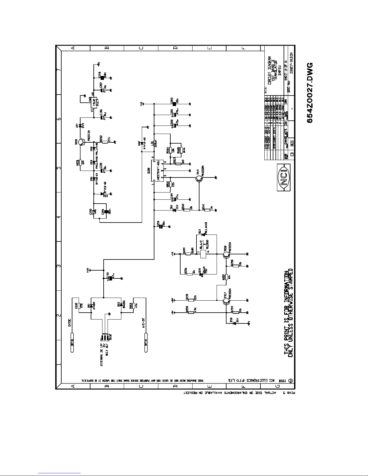
A/C Input supply:
The a/c input to the power supply module is provided by an external 24V a/c winding on the A/C
Mains transformer. The winding is connected to
rectifier
The resulting raw dc is routed via
indicates the presence of the a/c supply.
(D1)
is used to rectify the a/c input, with capacitors
Fuse F1
SK1 pin 1 and pin 3
C1
. A Full-wave Bridge
to C9 providing the smoothing.
(3 Amp) and Isolating diode D2 to
SK4. LED D4
+24V dc supply:
+24V
The
dc supply is connected to
The dc is routed via
Fuse F2
(3Amp) and Isolating diode
SK2 pin 1
with the return connected to
D3. LED D5
indicates the presence of
SK2 pin 2
.
the dc supply.
The combined supply at D2 and D3 cathode provides the power to the RF PA module via
and also to the MAIN PCB via
SK3
.
SK4
SK5 provides an output for a +12V Fan.
v
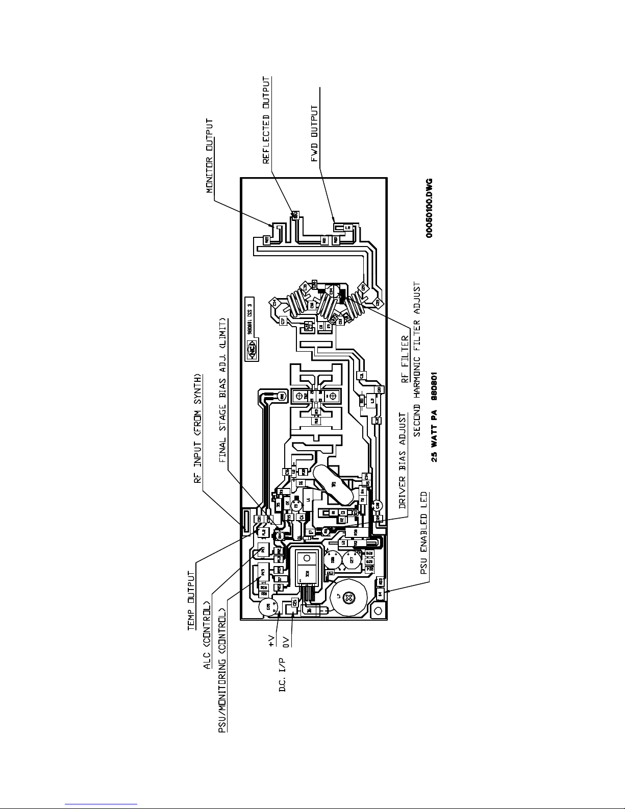
FMT RF PA Module (980801)
Issue 1A:
Page 28

FMT- 25 VHF FM TRANSLATOR 862-09725
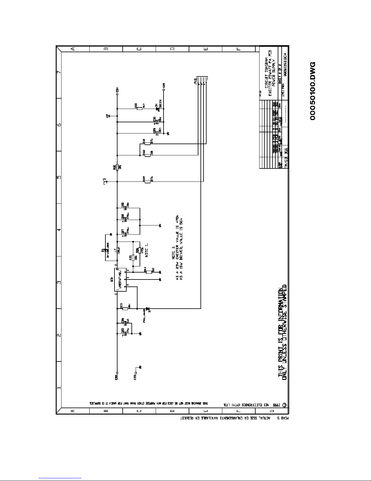
Power supply and regulation:
The power supply input to the RF PA Module is routed to a
Switch -mode regulator, IC2.
This
is a 3Amp device with built-in current limiting and requires +24V minimum and +45V maximum.
The output is set to +22.5V via
monitoring/enabling purposes.
R24/R25. PL5
LED D4
indicates the presence of the regulated supply.
is provided for current sensing (via R30) and
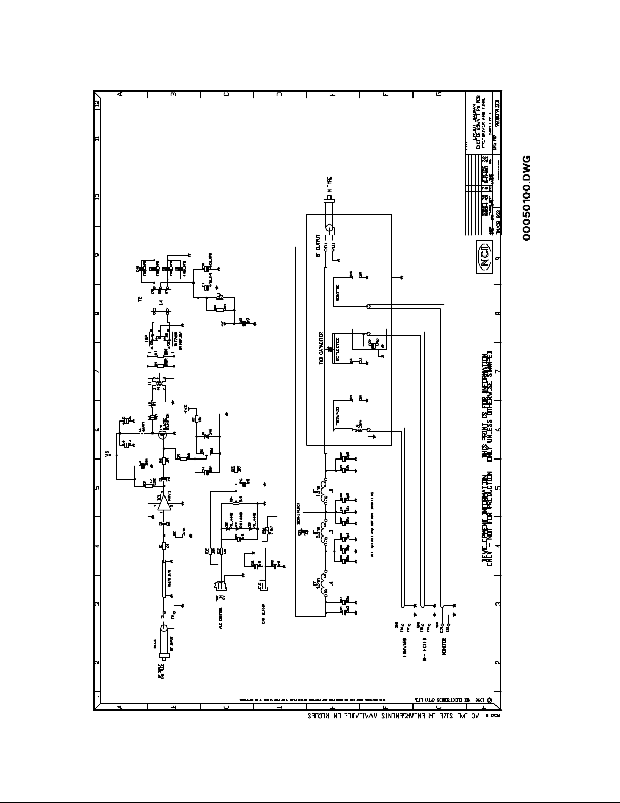
RF Power amplifier:
The
+6dBm
RF input is routed via
R1/R2
to a MMIC amplifier
IC1
. This amplifier gives a gain
of +11dB and provides drive to Mosfet TR1. The Gate voltage for TR1 is set via R6 and diode
D1 provides protection. The Mosfet operates in Class AB, with an operating current of 200mA
and Gate voltage of approximately 5V.
The output from
TR1
is routed via
coaxial cable. The transformer provides a balanced output to input of the Final RF stage
(Class ‘C’ Push-pull Mosfet). The gate bias voltage for this device is provided via
R14
is adjusted to limit the maximum output power of the device.
The output of
TR2
to unbalanced. The output from T2 is routed to the RF Low pass filter.
TR2
is routed to Wideband Transformer T2, which converts the balanced output of
The RF filter consists of a seventh order network
Band-reject circuit around L5. The Band reject section is adjustable via
C6/L2
to Wideband 4:1 transformer T1, which is made using
TR2
PL1/R14
(L4, L5, L6, C17, C18, C19 and C20)
C21
, which is normally
, and
with a
adjusted to 180MHz.
The filter attenuates all harmonics to ≤ -60dBc.
RF output coupler:
The output from the RF Filter is routed to a RF coupler (microstripline) that provides a
sample at
capacitors
E20/E21
C22
and
of the coupler section. The inductor
The RF output is provided by
Reflected
, a
C23
on the Forward and Reflected outputs flatten off the +6db/octave slope
sample via
L8
E14/E15
E18/E19
and a
Monitor
output via
provides the Monitor coupler with its flat response.
. The output power of the RF power stage is typically ≥ 25
Forward
E16/E17
. The
Watts.
Issue 1A:
Page 29

FMT- 25 VHF FM TRANSLATOR 862-09725
FMT-25
VHF FM TRANSLATOR
TECHNICAL MANUAL
Maintenance Information
Issue 1A:
Page 30
FMT- 25 VHF FM TRANSLATOR 862-09725
Issue 1A:
Page 31
FMT- 25 VHF FM TRANSLATOR 862-09725
Issue 1A:
Page 32
FMT- 25 VHF FM TRANSLATOR 862-09725
Issue 1A:
Page 33
FMT- 25 VHF FM TRANSLATOR 862-09725
Issue 1A:
Page 34
FMT- 25 VHF FM TRANSLATOR 862-09725
Issue 1A:
Page 35
FMT- 25 VHF FM TRANSLATOR 862-09725
Issue 1A:
Page 36
FMT- 25 VHF FM TRANSLATOR 862-09725
Issue 1A:
Page 37
FMT- 25 VHF FM TRANSLATOR 862-09725
Issue 1A:
Page 38
FMT- 25 VHF FM TRANSLATOR 862-09725
Issue 1A:
Page 39
FMT- 25 VHF FM TRANSLATOR 862-09725
Issue 1A:
Page 40
FMT- 25 VHF FM TRANSLATOR 862-09725
Issue 1A:
Page 41
FMT- 25 VHF FM TRANSLATOR 862-09725
Issue 1A:
Page 42
FMT- 25 VHF FM TRANSLATOR 862-09725
Issue 1A:
Page 43
FMT- 25 VHF FM TRANSLATOR 862-09725
Issue 1A:
Page 44
FMT- 25 VHF FM TRANSLATOR 862-09725
Issue 1A:
Page 45
FMT- 25 VHF FM TRANSLATOR 862-09725
Issue 1A:
Page 46
FMT- 25 VHF FM TRANSLATOR 862-09725
Issue 1A:
Page 47
FMT- 25 VHF FM TRANSLATOR 862-09725
Issue 1A:
Page 48
FMT- 25 VHF FM TRANSLATOR 862-09725
Issue 1A:
Page 49
FMT- 25 VHF FM TRANSLATOR 862-09725
Issue 1A:
Page 50
FMT- 25 VHF FM TRANSLATOR 862-09725
Issue 1A:
Page 51
FMT- 25 VHF FM TRANSLATOR 862-09725
Issue 1A:
Page 52
FMT- 25 VHF FM TRANSLATOR 862-09725
Issue 1A:
Page 53
FMT- 25 VHF FM TRANSLATOR 862-09725
Issue 1A:
 Loading...