


Unit 1 – Introduction
2. General Technical Descriptive:
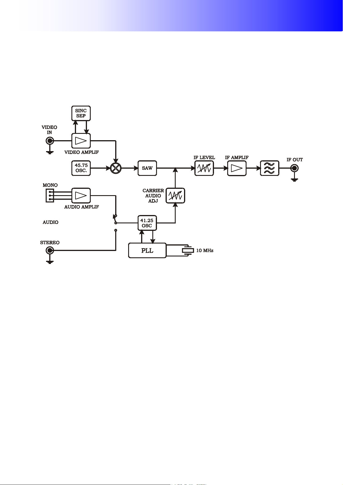
2.1. IF Modulator (for transmitter):
This is the input module. It is a professional audio and video modulator. The audio and video
signals are applied to their respective input for the modulation process in IF (41 to 47 MHz]. The audio
and video input impedances are 600 balanced Ohms and 75 unbalanced Ohms, respectively.
2.1.1. Video processing:
The video signal passes through linearity correction circuits and then is applied to the 45.75
MHz video modulator. There are Synchronizing Separation circuits that generate the auxiliary outputs
to “Automatic Circuits”. The video signal is also applied to a group delay predistortion circuit.
2.1.2. Audio processing:
The Mono-audio signal or stereo base band is applied to the module and modulates a 41.25
MHz audio carrier.
2.1.3 Module output:
Both carriers, audio and video modulated (41.25 and 45.75 MHz), are applied to the “Vestigial
Side Band Filter” (SAW Filter). At the output there is a circuit to control the IF output level.
2.2. UHF UP Converter:
2.2.1. Introduction:
This module converts an IF frequency signal into an UHF band channel, keeping its
characteristics and the same bandwidth.
2.2.2. IF filter and AGC amplifier (for transposer):
The IF amplifier and filter module establish the adequate bandwidth for the input signal and
supply the gain in this signal, keeping the level constant through an AGC loop.
2.2.3. Technical Descriptive:
The 2
Circuit), which frequency is selected through the DIP switch from the Oscillator control board. When
the modulated signal in IF is received in the 2
result of this mixing is filtered (channel filter) and supplied to the following modules of the equipment,
in the selected channel.
nd
UHF converter has an oscillator controlled by PLL (Phase Locked Loop Integrated
nd
converter, it is filtered and applied to a mixer. The
- 11 -

Unit 1 – Introduction
2.3. Amplifier Levels:
2.3.1. Comment/Composition/Origin:
The RTU1000T is composed of four 250W amplifier modules that are combined through 3dB
hybrid circuits. A 50W amplifier and 1: 4 hybrid module excite the final modules.
All the amplifiers are completely in solid state.
2.3.2. Protections/Signaling:
Each 250W amplifier has a VSWR protection (Voltage Stationary Wave Ratio), temperature and
limiting power. The output power, VSWR, temperature, current and module voltage can be monitored
through a DB9 connector in the front panel. In the frontal panel also there is the normal power
indication (Green Led), low power (red led) and excessive VSWR (red led). In the output there is the
video and audio power monitoring, antenna VSWR, power supply current and voltage, VSWR
indications, power supply temperature, signal absence, over voltage and over current.
2.4. Notch filter:
It is used to assure the operation of other transmitters in adjacent channels. It is composed by 7
mechanical cavities, 6 are syntonized in the spurious frequencies and 1 in the 2
nd
harmonic.
- 12 -
Unit 2 – IF Modulator
1. Audio and Video Modulator:
1.1. Function:
This module function is to generate two carriers: one in 45.75 MHz and the other in 41.25 MHz.
The first is modulated in AM-VSB by a video signal and the other one is modulated in frequency by an
audio signal.
1.2. Block Diagram:
1.3. Technical Description:
1.3.1. Video Modulator:
The transistor Q1 oscillates in the crystal frequency (45.75 MHz - IF video), and the transistor
Q2, with high input impedance, guarantees the isolation to the oscillator Q1 output. The frequency
accuracy is adjusted in the variable inductor L1. The input video signal, with adjustable level in R27
(front panel), is applied to the high impedance input push-pull amplifier formed by transistors Q6 and
Q9. The amplifier output signal modulates in amplitude, in the mixer M1, the video carrier.
The integrated circuits IC18 to IC21 form a group delay predistortion circuit. The syntonized
cells, at the video bandwidth, cause an advancement of 170 ns at 3.58MHz. This video pre-distortion is
inserted in the circuit through jump’s JP5 and JP6. The adjustable attenuator R146 allows equalizing
the video level when the pre-corrector circuit is turned off.
amplifier. This amplifier causes a non-linear enlargement to the video signal emphasizing the
synchronizing pulses. This signal is clamped in 0.7V by the D5 and is compared to 0.3V (due to diode
D4) in the comparator circuit IC6. In this manner, at the IC6 output, there will be only synchronizing
pulses. These pulses are applied to the IC5 (mono-stable) in the negative transition to generate
clamping pulses. The clamping pulses commute the transistor Q10 that switches the video signal
clamping it to the blanking level through R45. This adjustment allows choosing the point of modulation
in the mixer for a better linearity. If there is lack of clamping pulses, the Q11 transistor commutes,
allowing adjusting through R44 the level of the video carrier without modulation.
and commutes the transistor Q13. It allows switching the external circuits connected to the Automatic
output. The led in the panel shows this operation, when it is green it indicates video on. This circuit
presents about 60 seconds delay time approximately.
The transistor Q12 receives the video signal, invertes its phase and applies it to the IC7
The integrated circuit IC9B receives the clamping signal detected through D7, changes its state
- 2 -

Unit 2 – IF Modulator
The video signal peak is detected through IC8 and through IC9 and it is differentiated with the
level adjusted through R45, in order to extract the dc component.
The IC9A output has a dc level related to the video signal not taking into account the
synchronizing pulses. The 100% video measurement is adjusted through R72 in the meter with a video
signal with 100% APL. The C118 e L18 components form an ICPM corrector circuit that allows
correcting a non-desirable phase-shift at the video carrier caused by the modulating signal.
The modulated video carrier is amplified by IC1 and the SAW filter FL1 filters this signal giving
the final characteristics of the desired modulation, i.e., AM_VSB (amplitude modulation with vestigial
side band). The amplifiers IC2, IC3 and IC4 produce the necessary gain to signal, in order to
compensate the losses in SAW filter and deliver a 0 dBm output level. The output signal level is
adjustable by R12 (front panel), which controls the PIN diode conduction (D1). The trimpot R13 limits
the maximum IF output level and the circuit formed by transistor Q19 and capacitor C120 increases
slowly the output level to eliminate high frequency peaks when the equipment is turned on.
The IF signal, after amplification, passes through a low-pass filter, formed by L6, L7, C21, C22
and C23 to eliminate harmonic signals. Part of this signal is sent to the detector circuit formed by
transistors Q3 and Q4 to measure the IF signal in the panel. The trimpot R24 allows adjusting the
reading level through the meter.
1.3.2. Audio Modulator:
The transistor Q14 and associated components generate the audio carrier. The applied voltage
to the varicap diode D10 controls its frequency. The amplifiers IC12 and IC13 increase the signal level
and through the trimpot R108 is applied to the IF amplifier to be delivered at the output. A sample of
this signal is delivered to the “prescaler” IC14 through R108. It divides the signal into 64 and delivers it
to PLL (integrated IC15). The PLL divides again this signal, now into 66, and compares it with a
reference signal in phase, resulting a voltage proportional to the difference of the phase between the
signals; this voltage is filtered and applied to diode D10 to correct the frequency. The reference
frequency for PLL is generated at the integrated circuit itself that oscillates at 10 MHz and divides it
into 1024. The oscillator crystal is found in a thermal chamber, which is controlled by Q15 and by
thermistor NT1, for better frequency stability. The trimmer C90 allows the fine adjustment of this
carrier frequency (41.25 MHz). If the circuit cannot correct the frequency, the transistors Q17 and Q18
are commuted to turn on the frequency error red led.
The audio signal that will cause the modulation in frequency in this carrier may come from the
mono audio input or stereo audio input. It is possible to select it through jump JP3.
The mono audio input circuit has an unbalanced amplifier IC10 and pre-emphasis circuit. It is
possible to turn off the pre-emphasis through jump JP2. The trimpot R92 (front panel) adjusts the
audio level that will cause the correct modulation index. The integrated circuit IC17 and associated
components form a peak detector of audio signal and a trimpot R117 allows adjusting 100% at the
meter for the correct deviation. The battery input (+36V) through D16 and fuse F1 connects through
connector CN2 the power supply FTE017 (optional).
Obs: The circuit diagram is divided into four parts.
- 3 -
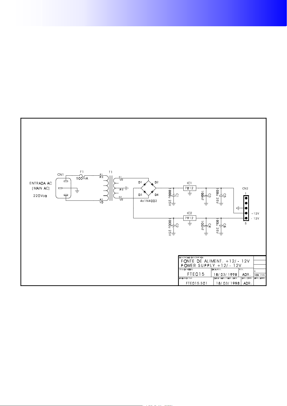
Unit 2 – IF Modulator
8. Power Supply:
8.1. Function:
The power supply function is to generate +12V and -12V voltage suitable to supply the
modulator.
8.2. Technical Description:
The transformer T1 reduces the input voltage for the rectifiers D1 to D4. The positive and
negative voltage obtained after the rectification and filtering through C1 and C2 are regulated through
IC1 and IC2 to obtain +12V and -12V voltage to supply the Modulator.
8.3. Circuit Diagram FTE015:
- 18 -
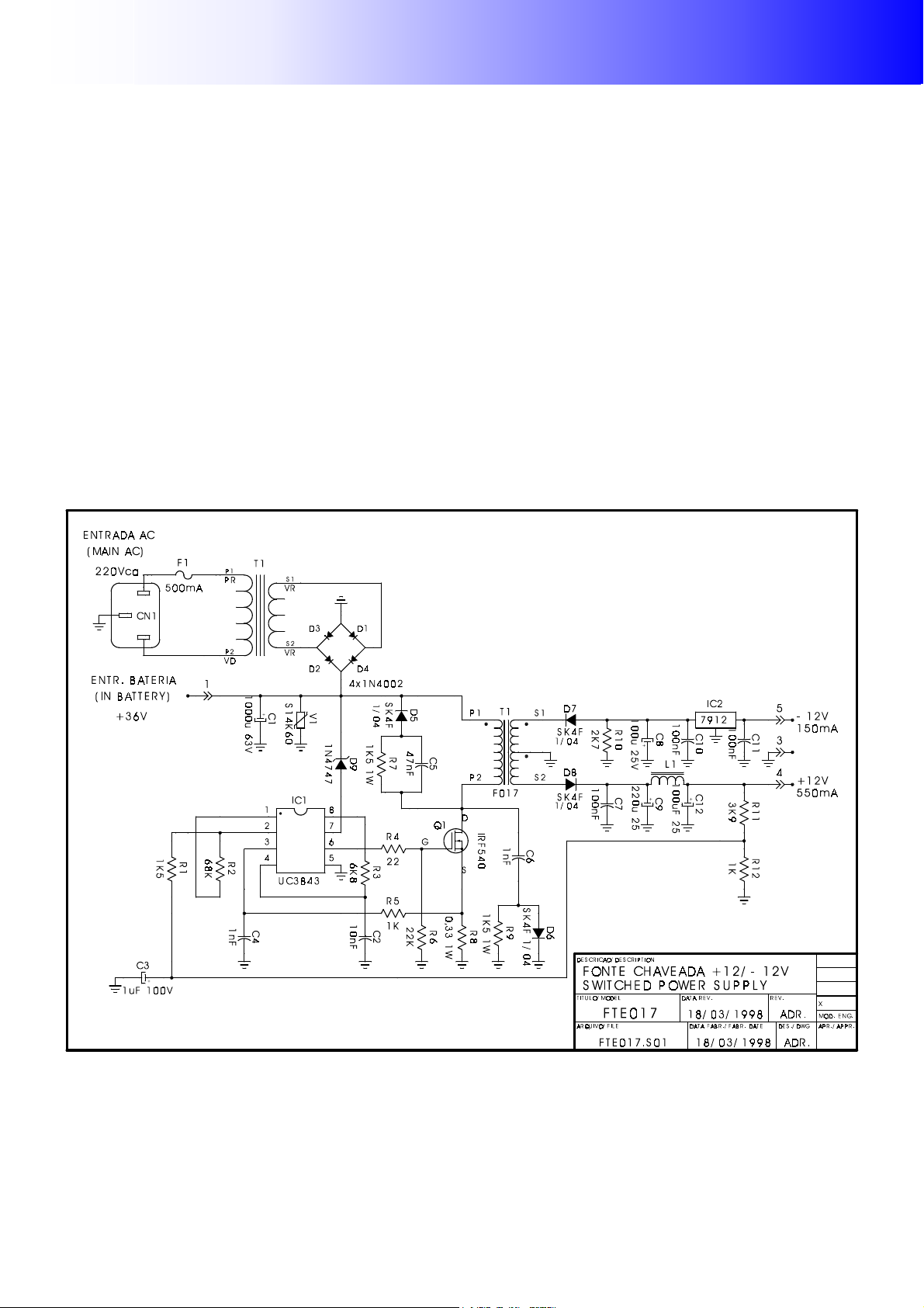
Unit 2 – IF Modulator
9. Power Supply (optional):
9.1. Function:
The switched power supply has the function to generate +12V and -12V voltages from the input
voltages AC or from the +36V battery (opc).
9.2. Technical Description:
The input voltage, after transformer T2 and diodes D1 and D4, supplies the PWM IC1. If there is
no AC the battery voltage supplies the circuit.
The pulses generated by IC1 commute the transistor Q1 and switch the voltage over the primary
T1 at 25 KHz frequency.
The induced pulses that are in the secondary are rectified by D7 and D8 and filtered by C8 e C9. The
regulator IC2 assures the -12V regulated voltage. A voltage sample after L1 supplies the IC1 control
input, through the divider R11 and R12. The pulses that are generated for IC1 have their width
changed in function of the received sample, canceling, in this manner, any variation in the +12V
voltage. The resistor R9 supplies a sampled voltage related to the current which circulates in the output
to the IC1, pin 3. This input protects the over current, reducing the +12V voltage.
9.3. Circuit diagram FTE017:
- 20 -
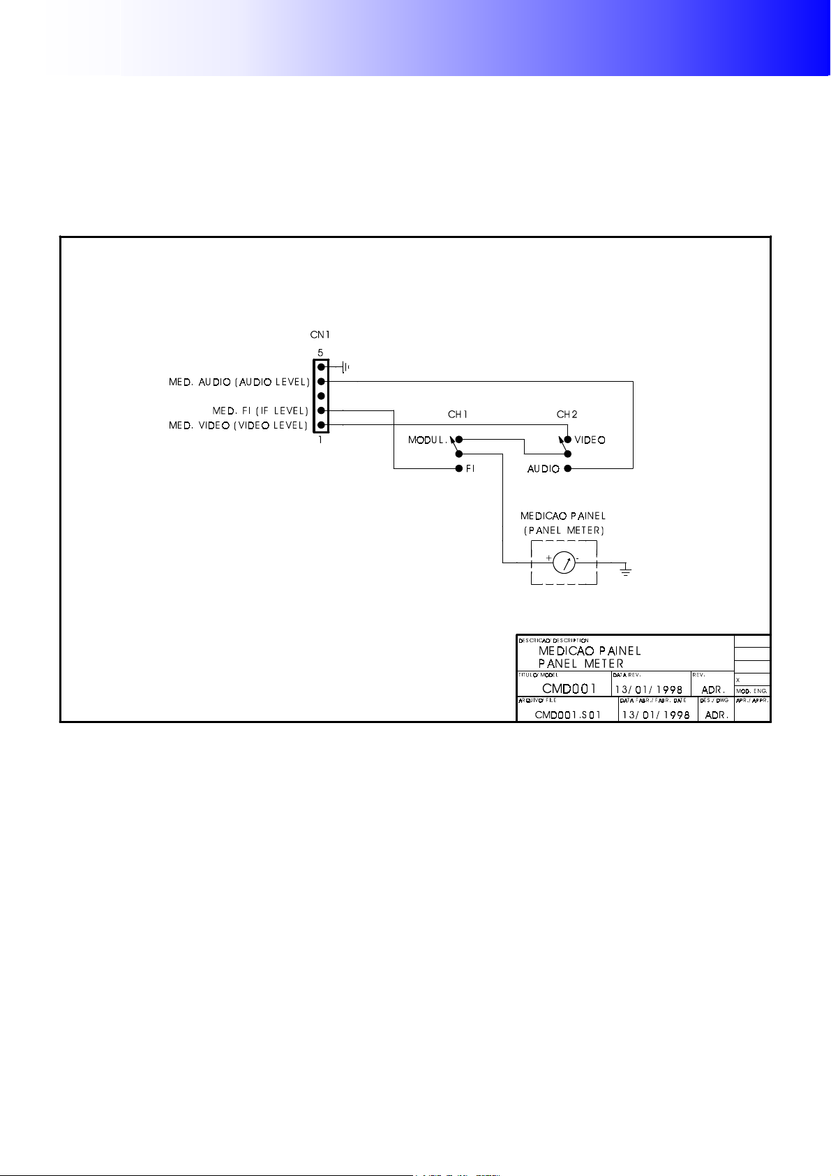
10. Meter Circuit:
10.1. Function:
The meter circuit allows, through the selector switches and meter, the measurements of the
video modulation, audio modulation and the IF level.
10.2. Circuit diagram CMD001:
Unit 2 – IF Modulator
- 23 -

Unit 3 – Channel UP Converter
1. Channel UP converter:
1.1. Introduction:
This module converts an IF signal, into “a” UHF band channel, maintaining its characteristics
and the same bandwidth.
1.2. IF filter and amplifier AGC (for transposer):
The filter and IF amplifier establish the necessary bandwidth to the input signal and supply a
gain in it, maintaining a constant level, through an AGC loop. It is used only in the transposer
equipments.
1.3. IF pre-distortion:
The IF module pre-distortion corrects the intermodulation, the differential gain, the differential
phase and the synchronism compression. This correction is done by pre-distortion on IF level (41-47
MHz). This module is placed after the audio and video modulator and before the channel converter
module.
1.4. Automatic Level Control (ALC):
This module maintains the output peak power at its nominal value, even if there is gain
variation due to the temperature and power supply variations.
It allows a maximum correction of ±1dB.
1.5. Channel converter:
The UHF channel UP converter has an oscillator that is controlled by PLL, whose frequency
operation is selected by DIP switch from the Local Oscillator control board, according to the channel
programming chart.
1.6. Protections/signals:
The channel UP converter has in its front panel a PLL (Phase Locked Loop) alarm led that shows
if the converter is out of the operation frequency.
- 2 -
Unit 3 – Channel UP Converter
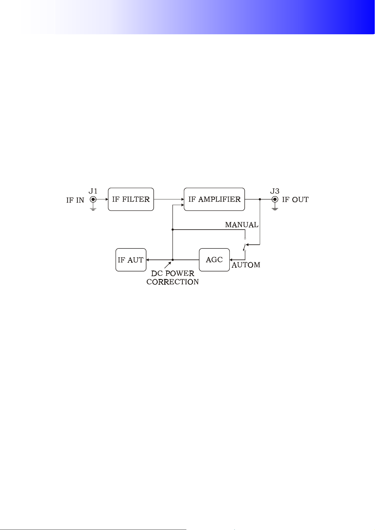
3. IF filter amplifier:
3.1. Function:
The IF filter establishes the adequate bandwidth to the input signal and the IF amplifier supplies
the gain for this signal, maintaining a constant level, through AGC loop.
3.2. Technical Characteristics:
Central Frequency __________________________________________________________________________ 44 MHz
Bandwidth __________________________________________________________________________________ 6 MHz
Input and Output impedance ______________________________________________________________ 50 Ohms
Maximum output level ______________________________________________________________________ +3 dBm
Linearity _________________________________________________________________ + or – 0.25 dB in ± 3 MHz
Maximum gain _______________________________________________________________________________ 60 dB
AGC band ____________________________________________________________________________________ 50 dB
Supply ______________________________________________________________________________ +12V at 250mA
3.3. Block Diagram:
3.4. Technical description:
3.4.1. IF Filter:
The input signal is applied by J1. The integrated circuit IC1 amplifies the applied signal to the
IF filter.
The function of the circuit that is formed by C7, L3, C8, C9, L4, C10, C11, L5, C12, C13, C14
and C16 is to determine the IF amplifier operation bandwidth. This filter is adjusted to obtain a 6MHz
bandwidth.
3.4.2. IF amplifier:
The IF signal received from IF filter is, through C17, connected to the adjustable attenuating
loop, that is formed by diodes D2, R9, D4 and D3. After the attenuating loop, the signal is amplified by
the integrated circuit MAR-7 (IC2).
The amplified signal passes through another attenuating loop, formed by diodes and resistors
D5, R14, D7 and D6, and it is connected by the capacitor C28 to the integrated circuit MAR-6 (IC3),
and finally, through capacitor C29, reaches the integrated circuit MAR-7 (IC4).
A sample signal from the output signal is taken from the resistor R45; after, it is amplified by
transistor Q4 and detected by the diodes D10 and D11. The detected signal by the diode D11 is
supplied, by the emitter follower Q3, to check the IF level in the panel.
The integrated circuit IC5-B supplies in its output a dc level, that is the function of the received
signal J1. The diode D1 and L9 act respectively in the polarization of the attenuating loops, altering the
final gain of the IF amplifier. When JP2 is in the AUT position, this dc level is proportional due to the
detected signal by the diode D10, maintaining the IF level constant in the output J3.
The IC5-A output level is the result of input levels voltage comparison between pins 3 and 2.
This way we can determine the operation point of the IF command adjusting R21. Through CN3-1 the
- 6 -

following circuits are enabled.
Unit 3 – Channel UP Converter
- 7 -

Unit 3 – Channel UP Converter
4. IF Pre-distortion linearity:
4.1. Function:
It corrects the non-linearity and/or intermodulation that are generated at the final stage of the
transmitter amplification.
4.2. Technical characteristics:
Frequency band: ______________________________________________________________________ 41 to 47 MHz
Input level: ____________________________________________________________________ -4.0 dBm ± 1.0 dBm
Output level (adj): __________________________________________________________________ + 3.0 dBm (max)
Input/Output Impedance:___________________________________________________________________ 50 ohm
Supply: _______________________________________________________________________________________ +25V
4.3. Technical Description:
IF signal applied to the input J1 is amplified by Q1, and in Q2 is divided in order to supply two
circuits, a linear one and a non-linear one.
The linear circuit has about a 40 ns delay line to compensate the delay caused in the non-linear
circuit. After the delay line, the signal is inserted through trimpot R13 in the adder circuit that is
formed by Q4 and Q5.
The non-linear circuit causes a distortion in the signal trough D3 and D4 that have its
conduction region determined by trimpots R11 and R29. This signal, distorted and amplified by Q7 and
Q8, is put in phase by equalizer circuit formed for L11, C29, R40 and R41, again amplified for Q9, via
trimpot R50 and transistor Q10 and finally is added to the linear signal.
The composed IF signal passes by the attenuator circuit, and its level is adjusted by R44, and
amplified by IC1 when it is delivered to output J2.
4.4. Adjustment Procedure:
The signal should be constantly checked by the spectrum analyzer using the red pattern
modulated signal.
1) Insert the circuit in the system when the IF level is about –3.0 dBm in the input and all the
trimpots are in the minimum.
2) Adjust trimpot R44 to 80% of its course approximately, then increase the level in R13 until
the nominal power is reached.
3) Adjust trimpots R11 and R29 in order to cause the needed distortion to cancel the distortion
that comes from the amplifying final stage, adjusting the level of this signal in the trimpot R50 and
compensating the power variation in the trimpot R13, in order to maintain it as a nominal one. Adjust
the inductor L11 to obtain the distorted signal phase inversion that will be inserted in the system.
- 12 -
 Loading...