


FEUL610Q421-06
ML610Q421/ML610Q422
ML610421
User’s Manual
Issue Date: Feb 9, 2015
Notes
1) The information contained herein is subject to change without notice.
2) Although LAPIS Semiconductor is continuously working to improve product reliability and quality, semiconductors
can break do wn and mal func ti on d ue to various factors. Therefore, in order to prevent personal injury or fire arising
from failure, please take safety measures such as complying with the derating characteristics, implementing
redundant and fire prevention designs, and utilizing backups and fail-safe procedures. LAPIS Semiconductor shall
have no respo nsibil ity fo r any d amages ar ising o ut of t he use o f our Pr oducts b eyond the rating sp eci fied b y LAPIS
Semiconductor.
3) Examples of application circu its, circuit constants and any other information contained herein are provided only to
illustrate the standard usage and operations of the Products.The peripheral conditions must be taken into account
when designing circuits for mass production.
4) The technical information specified herein is intended only to show the typical functions of the Products and
examples of application circuits for the Products. No license, expressly or implied, is granted hereby under any
intellectual property rights or other rights of LAPIS Semiconductor or any third party with respect to the
information contained in this document; therefore LAPIS Semiconductor shall have no responsibility whatsoever for
any dispute, concerning such rig hts owned by third parties, arising out of t he use of such technical infor matio n.
5) The Prod ucts are intended for use in general electronic equipment (i.e. AV/OA devices, communication, consumer
systems, gaming/entertainme nt sets) as well as the applications i nd ic a ted in this document.
6) The Products specified in this document are not designed to be radiation tolerant.
7) For use of our Products in applications requiring a high degree of reliability (as exemplified below), please contact
and consult with a LAPIS Semiconductor r epresentative: transportation eq uipment (i.e. cars, ships, trains), p rimary
communication equipment, traffic lights, fire/crime prevention, safet y equipment, medical systems, server s, solar
cells, and power transmission systems.
8) Do not use o ur Prod ucts in app lications req uiring ext remely hi gh reliabi lity, such as aeros pace equip ment, nuclear
power control systems, and submarine repeaters.
9) LAPIS Semiconductor shall have no responsibility for any damages or injury arising from non-compliance with the
recommended usage conditions and specifications contained herein.
10) LAPIS Semiconductor has used reasonable care to ensure the accuracy of the information contained in this
document. However, LAPIS Semiconductor does not warrant that such information is error-free and LAPIS
Semiconductor shall have no responsibility for any damages arising from any inaccuracy or misprint of such
information.
11) Please use the Products in accordance with any applicable environmental laws and regulations, such as the RoHS
Directive. For more details, including RoHS compatibility, please contact a ROHM sales office. LAPIS
Semiconductor shall have no responsibility for any damages or losses resulting non-compliance with any applicable
laws or regulations.
12) When providing our Products and technologies contained in this document to other countries, you must abide by
the procedures and provisions stipulated in all applicable exp ort laws and regulations, incl uding without limitation
the US Expo rt Administration R egulations and the Foreign Exchange and Foreign Trade Act.
13) This document, in part or in whole, may not be reprinted or reproduced without prior consent of LAPIS
Semiconductor.
Copyright 2009 - 2015 LAPIS Semiconductor Co., Ltd.
2-4-8 Shinyokohama, Kouhoku-ku,
Yokohama 222-8575, Japan
http://www.lapis-semi.com/en/

Preface
This manual describes the operation of the hardware of the 8-bit microcontroller
ML610Q421/ML610Q422/ML610421.
The following manuals are also available. Read them as necessary.
nX-U8/100 Core Instruction Manual
Description on the basic architecture and the each instruction of the nX-U8/100 Core.
MACU8 Assembler Package User’s Manual
Description on the method of operating the relocatable assembler, the linker, the
librarian, and the object converter and also on the specifications of the assembler
language.
CCU8 User’s Manual
Description on the method of operating the compiler.
CCU8 Progr amming Guide
Description on the method of programming.
CCU8 Language Refere nce
Description on the language specifications.
DTU8 Debugger User’s Manual
Description on the method of operating the debugger DTU8.
IDEU8 User’s Manual
Description on the integrated development environment IDEU8.
uEASE User’s Manual
Description on the on-chip debug tool uEASE.
uEASE connection Manual for ML610Q421/ML610Q422
Description about the connection between uEASE and ML610Q421/ML610Q422.
FWuEASE Flash Writer Host Program User’s Manual
Description on the Flash Writer host program.
Notation
MSB
LSB
R/W
R/W
R/W
R/W
R/W
R/W
R/W
R/W
R/W
Initial value
0 0 1 1 0 1 0 1
Bit name
Register name
Initial value after reset
Invalid bit: This bit reads “0” when read. Write to this bit is ignored.
Classification Notation Description
♦ Numeric val ue xxh, xxH Indicates a hexadecimal number. x: Any value in the range of 0 to F
xxb Indicates a binary number; “b” may be omitted. x: A value 0 or 1
♦ Unit word, W 1 word = 16 bits
byte, B 1 byte = 8 bits
nibble, N 1 nibble = 4 bits
maga-, M 10
kilo-, K 2
kilo-, k 10
milli-, m 10
micro-, µ 10
nano-, n 10
second, s (lower case) second
♦ Terminology “H” level, “1” level Indicates high voltage signal levels V
“L” level, “0” level Indicates low voltage signal levels V
♦ Register description
R/W: Indicates that Read/Wr ite a ttr ibute. “R” indicates that data can be read and “W” indicates that data can be written.
“R/W” indicates that data can be read or written.
6
10
= 1024
3
= 1000
-3
-6
-9
electrical characteristics.
electrical characteristics.
and VOH as specified by the
IH
and VOL as specified by the
IL
FCON0 OUTC1 OUTC0 OSCM1 OSCM0 SYSC1 SYSC0

ML610Q421/ML610Q422/ML610421 User’s Manual
Table of Content s
Chapter 1
1. Overview......................................................................................................................................................... 1-1
1.1 Features ....................................................................................................................................................... 1-1
1.2 Configuration of Functional Blocks ............................................................................................................ 1-5
1.2.1 Block Diagr am of ML610Q421 .......................................................................................................... 1-5
1.2.2 Block Diagr am of ML610Q422 .......................................................................................................... 1-6
1.2.3 Block Diagram of ML610421 ............................................................................................................. 1-7
1.3 Pins ............................................................................................................................................................. 1-8
1.3.1 Pin Layout ........................................................................................................................................... 1-8
1.3.1.1 Pin Layout of ML610Q421 120pin TQFP Package ........................................................................ 1-8
1.3.1.2 Pin Layout of ML610Q422 120pin TQFP Package ........................................................................ 1-9
1.3.1.3 Pin Layout of ML610Q421 Chip ................................................................................................... 1-10
1.3.1.4 Pin Layout of ML610Q422 Chip ................................................................................................... 1-11
1.3.1.5 Pin Layout of ML610421 Chip ...................................................................................................... 1-12
1.3.1.6 Pad Coordinates of ML610Q421 Chip .......................................................................................... 1-13
1.3.1.7 Pad Coordinates of ML610Q422 Chip .......................................................................................... 1-14
1.3.1.8 Pad Coordinates of ML610421 Chip ............................................................................................. 1-15
1.3.2 List of Pi n s ........................................................................................................................................ 1-16
1.3.2.1 List of ML610Q421/ML610Q422 Pins ........................................................................................ 1-16
1.3.2.2 List o f ML610421 Pins ................................................................................................................. 1-20
1.3.3 Description of Pins ............................................................................................................................ 1-24
1.3.4 Termination of Unused Pins ............................................................................................................. 1-28
Chapter 2
Contents
2. CPU and Memory Space ................................................................................................................................. 2-1
2.1 Overview..................................................................................................................................................... 2-1
2.2 Program Memory Space ............................................................................................................................. 2-1
2.3 Data Memory Space .................................................................................................................................... 2-2
2.4 Instruc tio n Le ngth ....................................................................................................................................... 2-2
2.5 Data Type .................................................................................................................................................... 2-2
2.6 Description of Register s .............................................................................................................................. 2-3
2.6.1 List of Register s .................................................................................................................................. 2-3
2.6.2 Data Segment Register (DSR) ............................................................................................................ 2-4
Chapter 3
3. Reset Function ................................................................................................................................................ 3-1
3.1 Overview..................................................................................................................................................... 3-1
3.1.1 Features ............................................................................................................................................... 3-1
3.1.2 Configuration ...................................................................................................................................... 3-1
3.1.3 List of Pi n............................................................................................................................................ 3-1
3.2 Description of Register s .............................................................................................................................. 3-2
3.2.1 List of Register s .................................................................................................................................. 3-2
3.2.2 Reset Status Register (RSTAT) .......................................................................................................... 3-2
3.3 Description of Operatio n............................................................................................................................. 3-3
3.3.1 Operation of System Reset Mode ....................................................................................................... 3-3
Contents – 1

ML610Q421/ML610Q422/ML610421 User’s Manual
Chapter 4
4. MCU Control Function ................................................................................................................................... 4-1
4.1 Overview..................................................................................................................................................... 4-1
4.1.1 Features ............................................................................................................................................... 4-1
4.1.2 Configuration ...................................................................................................................................... 4-1
4.2 Description of Register s .............................................................................................................................. 4-2
4.2.1 List of Register s .................................................................................................................................. 4-2
4.2.2 Stop Code Acceptor (STPACP) .......................................................................................................... 4-3
4.2.3 Standby Control Register (SBYCON) ................................................................................................ 4-4
4.2.4 Block Control Register 0 (BLKCON0)............................................................................................... 4-5
4.2.5 Block Control Register 1 (BLKCON1)............................................................................................... 4-6
4.2.6 Block Control Register 2 (BLKCON2)............................................................................................... 4-7
4.2.7 Block Control Register 3 (BLKCON3)............................................................................................... 4-8
4.2.8 Block Control Register 4 (BLKCON4)............................................................................................... 4-9
4.3 Description of Operation........................................................................................................................... 4-11
4.3.1 Program Run Mode ........................................................................................................................... 4-11
4.3.2 HALT Mode ..................................................................................................................................... 4-11
4.3.3 STOP Mode ...................................................................................................................................... 4-12
4.3.3.1 STOP Mode When CPU Operates with Low-Speed Clock ........................................................... 4-12
4.3.3.2 STOP Mode When CPU Operates with High-Speed Clock .......................................................... 4-13
4.3.3.3 Note on Return Operation from STOP/HALT Mode .................................................................... 4-14
4.3.4 Block Control Function ..................................................................................................................... 4-15
Chapter 5
Contents
5. Interrupts (INTs) ............................................................................................................................................. 5-1
5.1 Overview..................................................................................................................................................... 5-1
5.1.1 Features ............................................................................................................................................... 5-1
5.2 Description of Register s .............................................................................................................................. 5-2
5.2.1 List of Register s .................................................................................................................................. 5-2
5.2.2 Interrupt Enable Register 1 (IE1) ........................................................................................................ 5-3
5.2.3 Interrupt Enable Register 2 (IE2) ........................................................................................................ 5-4
5.2.4 Interrupt Enable Register 3 (IE3) ........................................................................................................ 5-5
5.2.5 Interrupt Enable Register 4 (IE4) ........................................................................................................ 5-6
5.2.6 Interrupt Enable Register 5 (IE5) ........................................................................................................ 5-7
5.2.7 Interrupt Enable Register 6 (IE6) ........................................................................................................ 5-8
5.2.8 Interrupt Enable Register 7 (IE7) ........................................................................................................ 5-9
5.2.9 Interrupt Request Register 0 (IRQ0) ................................................................................................. 5-10
5.2.10 Interrupt Request Register 1 (IRQ1) ................................................................................................. 5-11
5.2.11 Interrupt Request Register 2 (IRQ2) ................................................................................................. 5-12
5.2.12 Interrupt Request Register 3 (IRQ3) ................................................................................................. 5-13
5.2.13 Interrupt Request Register 4 (IRQ4) ................................................................................................. 5-14
5.2.14 Interrupt Request Register 5 (IRQ5) ................................................................................................. 5-15
5.2.15 Interrupt Request Register 6 (IRQ6) ................................................................................................. 5-16
5.2.16 Interrupt Request Register 7 (IRQ7) ................................................................................................. 5-17
5.3 Description of Operatio n........................................................................................................................... 5-18
5.3.1 Maskable Interrupt Processing .......................................................................................................... 5-19
5.3.2 Non-Maskable Interrupt Processing .................................................................................................. 5-19
5.3.3 Software Interrupt Processing ........................................................................................................... 5-19
5.3.4 Notes on Inte rrupt Rout ine ................................................................................................................ 5-20
5.3.5 Interrupt Disable State ...................................................................................................................... 5-23
Chapter 6
6. Clock Generation Cir cuit ................................................................................................................................ 6-1
6.1 Overview..................................................................................................................................................... 6-1
6.1.1 Features ............................................................................................................................................... 6-1
6.1.2 Configuration ...................................................................................................................................... 6-1
Contents – 2

ML610Q421/ML610Q422/ML610421 User’s Manual
6.1.3 List of Pi n s .......................................................................................................................................... 6-2
6.2 Description of Registers .............................................................................................................................. 6-2
6.2.1 List of Register s .................................................................................................................................. 6-2
6.2.2 Frequency Control Register 0 (FCON0) ............................................................................................. 6-3
6.2.3 Frequency Control Register 1 (FCON1) ............................................................................................. 6-5
6.3 Description of Operatio n............................................................................................................................. 6-6
6.3.1 Low-Speed Clock................................................................................................................................ 6-6
6.3.1.1 Low-Speed Clock Generation Circuit.............................................................................................. 6-6
6.3.1.2 Operation of Low-Speed Clock Generation Circuit ........................................................................ 6-7
6.3.2 High-Speed Clock ............................................................................................................................... 6-8
6.3.2.1 500 kHz RC Oscillation ................................................................................................................... 6-8
6.3.2.2 Crystal/Ceramic Oscillation Mode .................................................................................................. 6-9
6.3.2.3 Built-in PLL Oscillation Mode ...................................................................................................... 6-10
6.3.2.4 Exter nal Clock Input Mode ........................................................................................................... 6-10
6.3.2.5 Operation of High-Speed Clock Generation Circuit ...................................................................... 6-11
6.3.3 Switching of System Clock ............................................................................................................... 6-13
6.4 Specifying port r e gisters ........................................................................................................................... 6-15
6.4.1 Functioning P21 (OUTCLK) as the high speed clock output ........................................................... 6-15
6.4.2 Functioning P20 (LSCLK) as the low speed clock output ................................................................ 6-16
Chapter 7
Contents
7. Time Base Counter ......................................................................................................................................... 7-1
7.1 Overview..................................................................................................................................................... 7-1
7.1.1 Features ............................................................................................................................................... 7-1
7.1.2 Configuration ...................................................................................................................................... 7-1
7.2 Description of Register s .............................................................................................................................. 7-3
7.2.1 List of Register s .................................................................................................................................. 7-3
7.2.2 Low-Speed Time Base Counter (LTBR) ............................................................................................ 7-4
7.2.3 High-Speed Time Base Counter Divide Register (HTBDR) .............................................................. 7-5
7.2.4 Low-Speed Time Base Counter Frequency Adjustment Registers L and H
(LTBADJL, LTBADJH) ..................................................................................................................... 7-6
7.3 Description of Operatio n............................................................................................................................. 7-7
7.3.1 Low-Speed Time Base Counter .......................................................................................................... 7-7
7.3.2 High-Speed Time Base Counter ......................................................................................................... 7-8
7.3.3 Low-Speed Time Base Counter Frequency Adjustment Function ...................................................... 7-9
7.3.4 A signal generation for 16bit timer 2-3 fre q ue nc y mea sur e m e nt mod e ............................................ 7-10
Chapter 8
8. Capture ............................................................................................................................................................ 8-1
8.1 Overview..................................................................................................................................................... 8-1
8.1.1 Features ............................................................................................................................................... 8-1
8.1.2 Configuration ...................................................................................................................................... 8-1
8.1.3 List of Pins .......................................................................................................................................... 8-1
8.2 Description of Registers .............................................................................................................................. 8-2
8.2.1 List of Registers .................................................................................................................................. 8-2
8.2.2 Capture Control Register (C A PCON) ................................................................................................. 8-3
8.2.3 Capture Status Register (CAPSTAT).................................................................................................. 8-4
8.2.4 Capture Data Register 0 (CAPR0) ...................................................................................................... 8-5
8.2.5 Capture Data Register 1 (CAPR1) ...................................................................................................... 8-6
8.3 Description of Operation............................................................................................................................. 8-7
Chapter 9
9. 1 kHz Timer (1kHzTM) .................................................................................................................................. 9-1
9.1 Overview..................................................................................................................................................... 9-1
9.1.1 Features ............................................................................................................................................... 9-1
9.1.2 Configuration ...................................................................................................................................... 9-1
Contents – 3

ML610Q421/ML610Q422/ML610421 User’s Manual
9.2 Description of Registers .............................................................................................................................. 9-2
9.2.1 List of Registers .................................................................................................................................. 9-2
9.2.2 1 kHz Timer Count Registers (T1KCRL, T1K CRH).......................................................................... 9-3
9.2.3 1 kHz Timer Control Register (T1KCON) ......................................................................................... 9-4
9.3 Description of Operation............................................................................................................................. 9-5
Chapter 10
10. Timers ........................................................................................................................................................... 10-1
10.1 Overview................................................................................................................................................... 10-1
10.1.1 Features ............................................................................................................................................. 10-1
10.1.2 Configuration .................................................................................................................................... 10-1
10.2 Description of Registers ............................................................................................................................ 10-3
10.2.1 List of Register s ................................................................................................................................ 10-3
10.2.2 Timer 0 Data Register (TM0D) ........................................................................................................ 10-4
10.2.3 Timer 1 Data Register (TM1D) ........................................................................................................ 10-5
10.2.4 Timer 2 Data Register (TM2D) ........................................................................................................ 10-6
10.2.5 Timer 3 Data Register (TM3D) ........................................................................................................ 10-7
10.2.6 Timer 0 Counter Register (TM0C) ................................................................................................... 10-8
10.2.7 Timer 1 Counter Register (TM1C) ................................................................................................... 10-9
10.2.8 Timer 2 Counter Register (TM2C) ................................................................................................. 10-10
10.2.9 Timer 3 Counter Register (TM3C) ................................................................................................. 10-11
10.2.10 Timer 0 Control Register 0 (TM0CON0) ....................................................................................... 10-12
10.2.11 Timer 1 Control Register 0 (TM1CON0) ....................................................................................... 10-13
10.2.12 Timer 2 Control Register 0 (TM2CON0) ....................................................................................... 10-14
10.2.13 Timer 3 Control Re gister 0 (TM3CON0) ....................................................................................... 10-15
10.2.14 Timer 0 Control Register 1 (TM0CON1) ....................................................................................... 10-16
10.2.15 Timer 1 Control Register 1 (TM1CON1) ....................................................................................... 10-17
10.2.16 Timer 2 Control Register 1 (TM2CON1) ....................................................................................... 10-18
10.2.17 Timer 3 Control Register 1 (TM3CON1) ....................................................................................... 10-19
10.3 Description of Operation......................................................................................................................... 10-20
10.3.1 Timer mode operation ..................................................................................................................... 10-20
10.3.2 16-bit timer frequenc y measure ment mode operation ................................................................... 10-21
10.3.3 16-bit timer fr equency measurement mode application for setting uart baud-rate .......................... 10-23
Chapter 11
Contents
11. PWM ............................................................................................................................................................. 11-1
11.1 Overview................................................................................................................................................... 11-1
11.1.1 Features ............................................................................................................................................. 11-1
11.1.2 Configuration .................................................................................................................................... 11-1
11.1.3 List of Pi n s ........................................................................................................................................ 11-2
11.2 Description of Registers ............................................................................................................................ 11-2
11.2.1 List of Register s ................................................................................................................................ 11-2
11.2.2 PWM0 Period Registers (PW0PL, PW0PH) .................................................................................... 11-3
11.2.3 PWM0 Duty Registers (PW0DL, PW0DH) ...................................................................................... 11-4
11.2.4 PWM0 Count er Registers (PW0CH, PW0CL) ................................................................................. 11-5
11.2.5 PWM0 Control Register 0 (PW0CON0) ........................................................................................... 11-6
11.2.6 PWM0 Control Register 1 (PW0CON1) ........................................................................................... 11-7
11.3 Description of Ope ration........................................................................................................................... 11-8
11.4 Specifying port registers ......................................................................................................................... 11-10
11.4.1 Functioning P43 (PWM0) as the PWM output ............................................................................... 11-10
11.4.2 Functioning P34 (PWM0) as the PWM output ............................................................................... 11-11
Chapter 12
12. Watchdog Timer ........................................................................................................................................... 12-1
12.1 Overview................................................................................................................................................... 12-1
12.1.1 Features ............................................................................................................................................. 12-1
Contents – 4

ML610Q421/ML610Q422/ML610421 User’s Manual
12.1.2 Configuration .................................................................................................................................... 12-1
12.2 Description of Registers ............................................................................................................................ 12-2
12.2.1 List of Register s ................................................................................................................................ 12-2
12.2.2 Watchdog Timer Control Register (W DTCON) ............................................................................... 12-3
12.2.3 Watchdog Timer Mode Register (WDTMOD) ................................................................................. 12-4
12.3 Description of Ope ration........................................................................................................................... 12-5
12.3.1 Handli ng example when you do not want to use the watch dog timer .............................................. 12-7
Chapter 13
13. Synchronous Serial Port ................................................................................................................................ 13-1
13.1 Overview................................................................................................................................................... 13-1
13.1.1 Features ............................................................................................................................................. 13-1
13.1.2 Configuration .................................................................................................................................... 13-1
13.1.3 List of Pi n s ........................................................................................................................................ 13-2
13.2 Description of Registers ............................................................................................................................ 13-3
13.2.1 List of Register s ................................................................................................................................ 13-3
13.2.2 Serial Port Transmit/Receive Buffers (SIO0BUFL, SIO0BUFH) .................................................... 13-4
13.2.3 Serial Port Control Register (SI O0CON) .......................................................................................... 13-5
13.2.4 Serial Port Mode Register 0 (SIO0MOD0) ....................................................................................... 13-6
13.2.5 Serial Port Mode Register 1 (SIO0MOD1) ....................................................................................... 13-7
13.3 Description of Ope ration........................................................................................................................... 13-8
13.3.1 Transmit Operation ........................................................................................................................... 13-8
13.3.2 Receive Operation ............................................................................................................................. 13-9
13.3.3 Transmit/Receive Operation ........................................................................................................... 13-10
13.4 Specifying port registers ......................................................................................................................... 13-11
13.4.1 Functioning P42 (SOUT0), P41 (SCK0) and P40 (SIN0) as the SSIO/ “Master mode” ................ 13-11
13.4.2 Functioning P42 (SOUT0), P41 (SCK0) and P40 (SIN0) as the SSIO/ ”Slave mode” ................... 13-12
13.4.3 Functioning P46 (SOUT0), P45 (SCK0) and P44 (SIN0) as the SSIO/ ”Master mode” ................ 13-13
13.4.4 Functioning P46 (SOUT0), P45 (SCK0) and P44 (SIN0) as the SSIO/ ”Slave mode” ................... 13-14
Chapter 14
Contents
14. UART ........................................................................................................................................................... 14-1
14.1 Overview................................................................................................................................................... 14-1
14.1.1 Features ............................................................................................................................................. 14-1
14.1.2 Configuration .................................................................................................................................... 14-1
14.1.3 List of Pins ........................................................................................................................................ 14-1
14.2 Description of Registers ............................................................................................................................ 14-2
14.2.1 List of Register s ................................................................................................................................ 14-2
14.2.2 UART0 Transmit/Receive Buffer (UA0BUF) .................................................................................. 14-3
14.2.3 UART0 Contro l Register (UA0CON) .............................................................................................. 14-4
14.2.4 UART0 Mode Register 0 (UA0MOD0) ........................................................................................... 14-5
14.2.5 UART0 Mode Register 1 (UA0MOD1) ........................................................................................... 14-6
14.2.6 UART0 Baud Rate Registers L, H (UA0BRTL, UA0BRTH) .......................................................... 14-8
14.2.7 UART0 Status Re gister (UA0STAT) ............................................................................................... 14-9
14.3 Description of Ope ration......................................................................................................................... 14-11
14.3.1 Transfer Data Format ...................................................................................................................... 14-11
14.3.2 Baud Rate ........................................................................................................................................ 14-12
14.3.3 Transmit Data Direction ................................................................................................................. 14-13
14.3.4 Transmit Operation ......................................................................................................................... 14-14
14.3.5 Receive Operation ........................................................................................................................... 14-16
14.4 Specifying port registers ......................................................................................................................... 14-18
14.4.1 Functioning P43(TXD0) and P42(RXD0) as the UART ................................................................ 14-18
14.4.2 Functioning P43(TXD0) and P02(RXD0) as the UART ................................................................ 14-19
Contents – 5

ML610Q421/ML610Q422/ML610421 User’s Manual
Chapter 15
15. I2C Bus Interface ........................................................................................................................................... 15-1
15.1 Overview................................................................................................................................................... 15-1
15.1.1 Features ............................................................................................................................................. 15-1
15.1.2 Configuration .................................................................................................................................... 15-1
15.1.3 List of Pi n s ........................................................................................................................................ 15-1
15.2 Description of Registers ............................................................................................................................ 15-2
15.2.1 List of Registers ................................................................................................................................ 15-2
15.2.2 I
15.2.3 I
15.2.4 I
15.2.5 I
15.2.6 I
15.2.7 I
2
C Bus 0 Receive Register (I2C0RD) .............................................................................................. 15-3
2
C Bus 0 Slave Addr ess Register (I2C0SA) .................................................................................... 15-4
2
C Bus 0 Transmit Dat a Register (I2C0TD) .................................................................................... 15-5
2
C Bus 0 Control Register (I2C0CON) ............................................................................................ 15-6
2
C Bus 0 Mode Register (I2C0MOD) .............................................................................................. 15-7
2
C Bus 0 Status Register (I2C0STAT) ............................................................................................ 15-8
15.3 Description of Ope ration........................................................................................................................... 15-9
15.3.1 Communication Operating Mode ...................................................................................................... 15-9
15.3.1.1 Start Condition ............................................................................................................................... 15-9
15.3.1.2 Repeated Start Condition ............................................................................................................... 15-9
15.3.1.3 Slave Address Transmit Mode ....................................................................................................... 15-9
15.3.1.4 Data Transmit Mode ...................................................................................................................... 15-9
15.3.1.5 Data Receive Mode ....................................................................................................................... 15-9
15.3.1.6 Control Register Se tting Wait State ............................................................................................... 15-9
15.3.1.7 Stop Condition ............................................................................................................................. 15-10
15.3.2 Communication Operation Timing ................................................................................................. 15-11
15.3.3 Operation Waveforms ..................................................................................................................... 15-13
15.4 Specifying port registers ......................................................................................................................... 15-14
15.4.1 Functioning P41(SCL) and P40(SDA) as the I2C .......................................................................... 15-14
Chapter 16
Contents
16. NMI Pin ........................................................................................................................................................ 16-1
16.1 Overview................................................................................................................................................... 16-1
16.1.1 Features ............................................................................................................................................. 16-1
16.1.2 Configuration .................................................................................................................................... 16-1
16.1.3 List of Pi n s ........................................................................................................................................ 16-1
16.2 Description of Registers ............................................................................................................................ 16-2
16.2.1 List of Register s ................................................................................................................................ 16-2
16.2.2 NMI Data Register (NMID) .............................................................................................................. 16-3
16.2.3 NMI Control Register (NMICON).................................................................................................... 16-4
16.3 Description of Operation........................................................................................................................... 16-5
16.3.1 Interrupt Request ............................................................................................................................... 16-5
Chapter 17
17. Port 0 ............................................................................................................................................................. 17-1
17.1 Overview................................................................................................................................................... 17-1
17.1.1 Features ............................................................................................................................................. 17-1
17.1.2 Configuration .................................................................................................................................... 17-1
17.1.3 List of Pi n s ........................................................................................................................................ 17-1
17.2 Description of Registers ............................................................................................................................ 17-2
17.2.1 List of Register s ................................................................................................................................ 17-2
17.2.2 Port 0 Data Register (P0D) ............................................................................................................... 17-3
17.2.3 Port 0 Control Registers 0, 1 (P0CON0, P0CON1) .......................................................................... 17-4
17.2.4 External Interrupt Control Registers 0, 1 (EXICON0, EXICON1)................................................... 17-5
17.2.5 External Interrupt Control Register 2 (EXICON2) ........................................................................... 17-6
17.3 Description of Oper a tion........................................................................................................................... 17-7
17.3.1 External Interrupt/Capture Function ................................................................................................. 17-7
17.3.2 Interrupt Request ............................................................................................................................... 17-7
Contents – 6

ML610Q421/ML610Q422/ML610421 User’s Manual
Chapter 18
18. Port 1 ............................................................................................................................................................. 18-1
18.1 Overview................................................................................................................................................... 18-1
18.1.1 Features ............................................................................................................................................. 18-1
18.1.2 Configuration .................................................................................................................................... 18-1
18.1.3 List of Pi n s ........................................................................................................................................ 18-1
18.2 Description of Registers ............................................................................................................................ 18-2
18.2.1 List of Registers ................................................................................................................................ 18-2
18.2.2 Port 1 Data Register (P1D) ............................................................................................................... 18-3
18.2.3 Port 1 Control Registers 0, 1 (P1CON0, P1CON1) .......................................................................... 18-4
18.3 Description of Oper a tion........................................................................................................................... 18-5
18.3.1 Input Port Function ........................................................................................................................... 18-5
18.3.2 Secondary Function .......................................................................................................................... 18-5
Chapter 19
19. Port 2 ............................................................................................................................................................. 19-1
19.1 Overview................................................................................................................................................... 19-1
19.1.1 Features ............................................................................................................................................. 19-1
19.1.2 Configuration .................................................................................................................................... 19-1
19.1.3 List of Pi n s ........................................................................................................................................ 19-1
19.2 Description of Registers ............................................................................................................................ 19-2
19.2.1 List of Register s ................................................................................................................................ 19-2
19.2.2 Port 2 Data Register (P2D) ............................................................................................................... 19-3
19.2.3 Port 2 control registers 0, 1 (P2CON0, P2CON1) ............................................................................ 19-4
19.2.4 Port 2 Mode Register (P2MOD) ....................................................................................................... 19-5
19.3 Description of Oper a tion........................................................................................................................... 19-6
19.3.1 Output Port Function ......................................................................................................................... 19-6
19.3.2 Secondary Function .......................................................................................................................... 19-6
Chapter 20
Contents
20. Port 3 ............................................................................................................................................................. 20-1
20.1 Overview................................................................................................................................................... 20-1
20.1.1 Features ............................................................................................................................................. 20-1
20.1.2 Configuration .................................................................................................................................... 20-1
20.1.3 List of Pi n s ........................................................................................................................................ 20-2
20.2 Description of Registers ............................................................................................................................ 20-3
20.2.1 List of Register s ................................................................................................................................ 20-3
20.2.2 Port 3 data register (P3D).................................................................................................................. 20-4
20.2.3 Port 3 Direction Register (P3DIR) .................................................................................................... 20-5
20.2.4 Port 3 control registers 0, 1 (P3CON0, P3CON1) ............................................................................ 20-6
20.2.5 Port 3 mode registers 0, 1 (P3MOD0, P3MOD1) ............................................................................. 20-8
20.3 Description of Oper a tion......................................................................................................................... 20-10
20.3.1 Input/Output Port Functions............................................................................................................ 20-10
20.3.2 Secondary and Tertiary Functions .................................................................................................. 20-10
Chapter 21
21. Port 4 ............................................................................................................................................................. 21-1
21.1 Overview................................................................................................................................................... 21-1
21.1.1 Features ............................................................................................................................................. 21-1
21.1.2 Configuration .................................................................................................................................... 21-1
21.1.3 List of Pins ........................................................................................................................................ 21-2
21.2 Description of Registers ............................................................................................................................ 21-3
21.2.1 List of Register s ................................................................................................................................ 21-3
21.2.2 Port 4 Data Register (P4D) ............................................................................................................... 21-4
Contents – 7

ML610Q421/ML610Q422/ML610421 User’s Manual
21.2.3 Port 4 Direction Register (P4DIR) .................................................................................................... 21-5
21.2.4 Port 4 Control Registers 0, 1 (P4CON0, P4CON1) .......................................................................... 21-6
21.2.5 Port 4 Mode Registers 0, 1 (P4MOD0, P4MOD1) ........................................................................... 21-8
21.3 Description of Oper a tion......................................................................................................................... 21-11
21.3.1 Input/Output Port Functions............................................................................................................ 21-11
21.3.2 Secondary and Tertiary Functions .................................................................................................. 21-11
Chapter 22
22. Port A ............................................................................................................................................................ 22-1
22.1 Overview................................................................................................................................................... 22-1
22.1.1 Features ............................................................................................................................................. 22-1
22.1.2 Configuration .................................................................................................................................... 22-1
22.1.3 List of Pi n s ........................................................................................................................................ 22-1
22.2 Description of Registers ............................................................................................................................ 22-2
22.2.1 List of Register s ................................................................................................................................ 22-2
22.2.2 Port A Data Register (PAD).............................................................................................................. 22-3
22.2.3 Port A Direction Register (PADIR) .................................................................................................. 22-4
22.2.4 Port A Control Registers 0, 1 (PACON0, PACON1) ....................................................................... 22-5
22.3 Description of Operation........................................................................................................................... 22-7
22.3.1 Input/Output Port Functions.............................................................................................................. 22-7
Chapter 23
Contents
23. Melody Driver .............................................................................................................................................. 23-1
23.1 Overview................................................................................................................................................... 23-1
23.1.1 Features ............................................................................................................................................. 23-1
23.1.2 Configuration .................................................................................................................................... 23-1
23.1.3 List of Pi n s ........................................................................................................................................ 23-1
23.2 Description of Registers ............................................................................................................................ 23-2
23.2.1 List of Register s ................................................................................................................................ 23-2
23.2.2 Melody 0 Control Register (MD0CON) ........................................................................................... 23-3
23.2.3 Melody 0 Tempo Code Register (MD0TMP) ................................................................................... 23-4
23.2.4 Melody 0 Scale Code Register (MD0TON) ...................................................................................... 23-5
23.2.5 Melody 0 Tone Length Code Register (MD0LEN) .......................................................................... 23-6
23.3 Description of Ope ration........................................................................................................................... 23-7
23.3.1 Operation of Melody Output ............................................................................................................. 23-7
23.3.2 Tempo Codes .................................................................................................................................... 23-8
23.3.3 Tone Length Codes ........................................................................................................................... 23-9
23.3.4 Scale Codes ..................................................................................................................................... 23-10
23.3.5 Example of Using Melo dy Circuit .................................................................................................. 23-11
23.3.6 Operations of Buzzer Output .......................................................................................................... 23-12
23.4 Specifying port registers ......................................................................................................................... 23-13
23.4.1 Functioning P22 (MD0) as the Melody or Buzzer output ............................................................... 23-13
Chapter 24
24. RC Oscillation Type A/D Con ver te r ............................................................................................................. 24-1
24.1 Overview................................................................................................................................................... 24-1
24.1.1 Features ............................................................................................................................................. 24-1
24.1.2 Configuration .................................................................................................................................... 24-1
24.1.3 List of Pi n s ........................................................................................................................................ 24-2
24.2 Description of Registers ............................................................................................................................ 24-3
24.2.1 List of Registers ................................................................................................................................ 24-3
24.2.2 RC-ADC Counter A Registers (RADCA0–2) .................................................................................. 24-4
24.2.3 RC-ADC Counter B Registers (RADCB0–2) ................................................................................... 24-5
24.2.4 RC-ADC Mode Register (RADMOD) .............................................................................................. 24-6
24.2.5 RC-ADC Control Register (RADCO N) ............................................................................................ 24-7
24.3 Description of Oper a tion........................................................................................................................... 24-8
Contents – 8

ML610Q421/ML610Q422/ML610421 User’s Manual
24.3.1 RC Oscillator Circuits ....................................................................................................................... 24-8
24.3.2 Counter A/Counter B Reference Modes ......................................................................................... 24-11
24.3.3 Example of Use of RC Oscillation Type A/D Converter ................................................................ 24-15
24.3.4 Monitoring RC Oscillation.............................................................................................................. 24-20
24.4 Specifying port registers ......................................................................................................................... 24-21
24.4.1 Functioning P35(RCM), P34(RCT0), P33(RT0), P32(RS0), P31(CS0) and P30(IN0) as the
RC-ADC(Ch0) ................................................................................................................................ 24-21
24.4.2 Functioning P47(RT1), P46(RS1), P45(CS1) and P44(IN1) as the RC-ADC(Ch1) ....................... 24-22
Chapter 25
25. Successive Approximation Type A/D Converter .......................................................................................... 25-1
25.1 Overview................................................................................................................................................... 25-1
25.1.1 Features ............................................................................................................................................. 25-1
25.1.2 Configuration .................................................................................................................................... 25-1
25.1.3 List of Pi n s ........................................................................................................................................ 25-2
25.2 Description of Registers ............................................................................................................................ 25-3
25.2.1 List of Register s ................................................................................................................................ 25-3
25.2.2 SA-ADC Result Registe r 0L (SADR0L) .......................................................................................... 25-4
25.2.3 SA-ADC Result Registe r 0H (SADR0H) ......................................................................................... 25-4
25.2.4 SA-ADC Result Registe r 1L (SADR1L) .......................................................................................... 25-5
25.2.5 SA-ADC Result Registe r 1H (SADR1H) ......................................................................................... 25-5
25.2.6 SA-ADC Control Regis t er 0 (SADCON0) ....................................................................................... 25-6
25.2.7 SA-ADC Control Regis t er 1 (SADCON1) ....................................................................................... 25-7
25.2.8 SA-ADC Mode Register 0 (SADMOD0) ......................................................................................... 25-8
25.3 Description of Oper a tion........................................................................................................................... 25-9
25.3.1 Settings of A/D Convers i on Channel s ................................................................................................ 25-9
25.3.2 Operation of the Successive Approximation A/D Converter .......................................................... 25-10
Chapter 26
Contents
26. LCD Drivers ................................................................................................................................................. 26-1
26.1 Overview................................................................................................................................................... 26-1
26.1.1 Features ............................................................................................................................................. 26-3
26.1.2 Configurati on of the L CD Drivers .................................................................................................... 26-4
26.1.3 Configurati on of the Bias Generation Circuit ................................................................................... 26-5
26.1.4 List of Pi n s ........................................................................................................................................ 26-6
26.2 Description of Registers ............................................................................................................................ 26-9
26.2.1 List of Register s ................................................................................................................................ 26-9
26.2.2 Bias Circuit Control Register 0 (BIASCON) .................................................................................. 26-10
26.2.3 Display Control Register (DSP CNT) .............................................................................................. 26-11
26.2.4 Display Mode Register 0 (DSPMOD0) .......................................................................................... 26-12
26.2.5 Display Mode Register 1 (DSPMOD1) .......................................................................................... 26-14
26.2.6 Display Control Register (DSPCON) ............................................................................................. 26-15
26.2.7 Display Allocation Register A (DS0C0A to DS49C7A) ................................................................ 26-16
26.2.8 Display Allocation Register B (DS0C0B to DS49C7B) ................................................................. 26-18
26.2.9 Display Registers (DSPR00 to DSPR71) ........................................................................................ 26-20
26.3 Description of Oper a tion......................................................................................................................... 26-25
26.3.1 Operation of LCD Drivers and Bias Generation Circuit ................................................................. 26-25
26.3.2 Segment Mapping When the Programmable Display Allocation Function is Not Used ................ 26-26
26.3.3 Segment Mapping Whe n the Programmable Display Allocation Function is Used ....................... 26-27
26.3.4 Common Output Waveforms .......................................................................................................... 26-29
26.3.5 Segment Output Waveforms ........................................................................................................... 26-31
Chapter 27
27. Battery Level Detector .................................................................................................................................. 27-1
27.1 Overview................................................................................................................................................... 27-1
27.1.1 Features ............................................................................................................................................. 27-1
Contents – 9

ML610Q421/ML610Q422/ML610421 User’s Manual
27.1.2 Configuration .................................................................................................................................... 27-1
27.2 Description of Registe r s ............................................................................................................................ 27-2
27.2.1 List of Register s ................................................................................................................................ 27-2
27.2.2 Battery Level Detector Control Register 0 (BLDCON0) .................................................................. 27-3
27.2.3 Battery Level Detector Control Register 1 (BLDCON1) .................................................................. 27-4
27.3 Description of Oper a tion........................................................................................................................... 27-5
27.3.1 Threshold Voltage ............................................................................................................................. 27-5
27.3.2 Operation of Battery Level Detector ................................................................................................. 27-6
Chapter 28
28. Power Supply Circuit .................................................................................................................................... 28-1
28.1 Overview................................................................................................................................................... 28-1
28.1.1 Features ............................................................................................................................................. 28-1
28.1.2 Configuration .................................................................................................................................... 28-1
28.1.3 List of Pi n s ........................................................................................................................................ 28-1
28.2 Description of Oper a tion........................................................................................................................... 28-2
Chapter 29
29. On-Chip Debug Function .............................................................................................................................. 29-1
29.1 Overview................................................................................................................................................... 29-1
29.2 Method of Connecting to On-Chip Debug Emulator ................................................................................ 29-1
29.3 Flash Memor y Rewrite Function .............................................................................................................. 29-2
Appendixes
Contents
Appendix A Registers ......................................................................................................................................... A-1
Appendix B Package Dimensions ........................................................................................................................B-1
Appendix C Electrical Characteristics .................................................................................................................C-1
Appendix D Application Circuit Example .......................................................................................................... D-1
Appendix E Check List ........................................................................................................................................ E-1
Revision History
Revision History .....................................................................................................................................................R-1
Contents – 10

Chapter 1
Overview

1. Overview
1.1 Features
ML610Q421/ML610Q422/ML610421 User’s Manual
Chapter 1 Overview
This LSI is a high-performance 8-bit CMOS microcontroller into which rich peripheral circuits, such as synchronous
serial port, UART, I
converter, 12-bit successive approximation type A/D converter, and LCD d river, are incorporated around 8-bit CPU
nX-U8/100.
The CPU nX-U8/100 is capable of efficient instruction execution in 1-intruction 1-clock mode by 3-stage pipe line
architecture parallel procesing.
The Flash ROM that is installed as program memory to ML610Q421/ML610Q422 achieves low-voltage low-power
consumption operation (read operation) equivalent to mask ROM and is most suitable for battery-driven applications.
The on-chip debug function that is installed enables program debugging and programming.
• CPU
− 8-bit RISC CPU (CPU name: nX-U8/100)
− Instruction system: 16-bit instructions
− Instruction set: Transfer, arithmetic operations, comparison, logic operations, multiplication/division, bit
− On-Chip debug function(ML610Q421/ML610Q422 only)
− Minimum instruction execution time
30.5 µs (@32.768 kHz system clock)
0.24 4µs (@4.096 MHz system clock)
• Internal memory
− ML610Q421/ML610Q422:Internal 32KByte Flash ROM (16K×16 bits) (including unus able 1KByte TEST ar ea)
− ML610421:Internal 32KByte Mask ROM (16K×16 bits) (including unusable 1KByte TEST area)
− Internal 1KByte Data RAM (1024×8 bits), 1KByte Display Allocation RAM (1024 x 8bit)
− Internal 100-byte RAM for display
• Interrupt controller
− 2 non-maskable interrupt sources (Internal source: 1, External source: 1)
− 20 maskable interrupt sources (Internal sources: 16, External sources: 4)
• Time base counter
− Low-speed time base counter ×1 channel
Frequency compensation (Compensation range: Approx. −488ppm to +488ppm. Compensation accuracy: Approx.
0.48ppm)
− High-speed time base counter ×1 channel
• Watchdog timer
− Non-maskable interrupt and reset
− Free running
− Overflow period: 4 types selectable (125ms, 500ms, 2s, and 8s)
• Timers
− 8 bits × 4 channels (Timer0-3: 16-bit x 2 configura tion available by using Timer0-1 or Timer2-3)
Clock frequency measurement mode (in one channel of 16-bit configurat i on using Timer2-3)
−
• 1 kHz timer
− 10 Hz/1 Hz interrup t function
2
C bus interface (master), melody driver, battery level detect circuit, RC oscillation type A/D
manipulations, bit logic operations, jump, conditional jump, call return stack manipulations,
arithmetic shift, and so on
1 – 1

ML610Q421/ML610Q422/ML610421 User’s Manual
• Capture
− Time base capture × 2 channels (4096 Hz to 32 Hz)
• PWM
− Resolution 16 bits × 1 channel
• Synchronous ser i al port
− Master/slave selectable
− LSB first/MSB first selectable
− 8-bit length/16-bit length selectable
• UART
− Half-Duplex Communication
− TXD/RXD × 1 channel
− Bit length, parity/no parity, odd pa rity/even parity, 1 stop bit/2 stop bits
− Positive logic/negative logic selectable
− Built-in baud rate generator
2
C bus interface
• I
− Maste r function only
− Fast mode (400 kbps@4MHz), standard mode (100 kbps@1MHz, 50kbps@500kHz)
• Melody driver
− Scale: 29 types (Melody sound frequency: 508 Hz to 32.768 kHz)
− To ne length: 63 types
− Tempo: 15 types
− Buzzer output mode (4 output modes, 8 frequencies, 16 duty levels)
• RC oscillation type A/D converter
− 24-bit counter
− Time division × 2 channels
• Successive approximation type A/D converter
− 12-bit A/D converter
− Input × 2 channels
• General-purpose ports
− Non-maskable interrupt input port × 1 channel
− Input-only port × 6 channels (includ i ng s econdary functions)
− Output-only port × 3 channels (includ ing secondary functi ons)
− Input/output port
ML610Q421/ML610421: 22 channels (including second ary functions)
ML610Q422: 14 channels (including sec ondary functions)
Chapter 1 Overview
1 – 2

ML610Q421/ML610Q422/ML610421 User’s Manual
Chapter 1 Overview
• LCD driver
− Dot matrix can be supported.
ML610Q421/ML610421: 400 dots max. (50 seg × 8 com), 1/1 to 1/8 duty
ML610Q422: 800 dots max. (50 seg × 16 com), 1/1 to 1/16 duty
− 1/3 or 1/4 bias (built-in bias generation circuit)
− Frame frequency selecable (approx. 64 Hz, 73 Hz, 85 Hz, and 102 Hz)
− Bias voltage multiplying clock selectable (8 types)
− Contrast adjustment (1/3 bias: 32 steps, 1/4 bias: 20 steps)
− LCD drive stop mode, LCD display mode, all LCDs on mode, and all LCDs off mode selectable
− Programmable display allocation function (available o nly when 1/1~1/8 duty is selected)
• Reset
− Reset through the RESET_N pin
− Power-on reset generation when powered on
− Reset when oscillation stop of the low-speed clock is detected
− Reset by the watchdog timer (WDT) overflow
• Power supply voltage detect function
− Judgment voltages: One of 16 levels
− Judgment accuracy: ±2% (Typ.)
• Clock
− Low-speed clock: (This LSI can not guarantee the operation withoug low-speed clock)
Crystal oscillation (32.768 kHz)
− High-speed clock:
Built-in RC oscillation (500 kHz)
Built-in PLL oscillation (8.192 MHz ±2.5%), crystal/ceramic oscillation (4.096 MHz), external clock
− Selection of high-speed clock mode by software:
Built-in RC oscillation, built-in PLL oscillation, cr ystal/ceramic oscillation, external clock
• Power management
− HALT mode: Instruction exec ution by CPU is suspend e d (peripheral circuits are in operating states).
− STOP mode: Stop of low-speed oscillation and high-speed oscillation (Operations of CPU and peripheral circuits
are stopped.)
− Clock gear: The frequenc y of high-speed system clock can be changed by software (1/1, 1/2, 1/4, or 1/8 of the
oscillation clock)
− Block Control Function: Power down (reset registers and stop clock supply) the circuits of unused peripherals.
• Guaranteed operating range
− Operating temperature: −20°C to 70°C (P version: −40°C to +85°C)
− Operating voltage: V
= 1.1V to 3.6V, AVDD = 2.2V to 3.6V
DD
1 – 3
ML610Q421/ML610Q422/ML610421 User’s Manual
ML610Q421-xxxWA
Flash ROM
-20°C to +70°C
Yes
ML610422-xxxWA
Mask ROM
-20°C to +70°C
-
ML610Q421-xxxTB
Flash ROM
-20°C to +70°C
Yes
ML610Q422P-xxxTB
Flash ROM
-40°C to +85°C
Yes
• Product name – Supported Function
The line-up of the ML610Q421 ,the ML610Q422 and the ML610421 is below.
Chapter 1 Overview
- Chip (Die) - ROM type
ML610Q422-xxxWA Flash ROM -20°C to +70°C Yes
ML610Q421P-xxxWA Flash ROM -40°C to +85°C Yes
ML610Q422P-xxxWA Flash ROM -40°C to +85°C Yes
ML610421-xxxWA Mask ROM -20°C to +70°C Yes
ML610421P-xxxWA Mask ROM -40°C to +85°C ML610422P-xxxWA Mask ROM -40°C to +85°C -
Operating
temperature
Product availability
-120-pin plastic
TQFP -
ML610Q422-xxxTB Flash ROM -20°C to +70°C Yes
ML610Q421P-xxxTB Flash ROM -40°C to +85°C Yes
ML610421-xxxTB Mask ROM -20°C to +70°C ML610422-xxxTB Mask ROM -20°C to +70°C ML610421P-xxxTB Mask ROM -40°C to +85°C ML610422P-xxxTB Mask ROM -40°C to +85°C -
ROM type
Operating
temperature
Product availability
xxx: ROM code numbe r (xxx of the blank product is NNN)
Q: Flash ROM version
P: Wide range temperature version (P version)
WA: Chip (Die),
TB: TQFP
1 – 4
1.2 Configuration of Functional Blocks
Program
SSIO
SCK0*
SIN0*
SOUT0*
UART
RXD0*
TXD0*
I2C
SDA*
SCL*
INT
1
RAM
Interrupt
CPU (nX-U8/100)
Timing
EA
SP
On-Chip
Instruction
BUS
Instruction
TBC
INT 4 INT 1 INT 1 INT
1
WDT
INT
4
8bit Timer
Capture
INT
1
PWM
P00 to P03
P10 to P11
P20 to P22
INT 5 NMI
P30 to P35
P40 to P47
PA0 to PA7
Data-bus
PWM0*
Melody
INT 1 MD0*
TEST
RESET_N
XT0
XT1
OSC0*
OSC1*
LSCLK*
OUTCLK*
BLD
Power
AVDD
AVSS
V
LCD
COM0 to COM7
SEG0 to SEG49
LCD
VL1, VL2, VL3, VL4
C1, C2, C3, C4
12bit-ADC
AIN0, AIN1
V
REF
CS0*
IN0*
RS0*
RT0*
CRT0*
RCM*
CS1*
IN1*
RS1*
RT1*
RESET &
ALU
EPSW1~3
PSW
ELR1~3
LR
ECSR1~3
DSR/CSR
PC
GREG
VPP
VDD
VSS
V
DDX
1kHzTC
INT 1 INT 1 INT
1
Display RAM
100Byte
Display Allocation
RAM 1024Byte
1.2.1 Block Diagram of ML610Q421
Controller
ICE
TEST
OSC
DDL
RC-ADC
×2
* Secondary function or Tertiary function
0~15
Decoder
Register
1024byte
Controller
ML610Q421/ML610Q422/ML610421 User’s Manual
Chapter 1 Overview
Controller
×2
×4
Memory
(Flash)
32Kbyte
GPIO
Driver
BIAS
Figure 1-1 Block Diagram of ML610Q421
1 – 5

1.2.2 Block Diagram of ML610Q422
Program
SSIO
SCK0*
SIN0*
SOUT0*
UART
RXD0*
TXD0*
I2C
SDA*
SCL*
INT
1
RAM
Interrupt
CPU (nX-U8/100)
Timing
EA
SP
On-Chip
Instruction
BUS
Instruction
TBC
INT 4 INT 1 INT 1 INT
1
WDT
INT
4
8bit Timer
Capture
2
INT
1
PWM
P00 to P03
P10 to P11
P20 to P22
INT 5 NMI
P30 to P35
P40 to P47
Data-bus
PWM0*
Melody
INT 1 MD0*
TEST
RESET_N
XT0
XT1
OSC0*
OSC1*
LSCLK*
OUTCLK*
BLD
Power
AVDD
AVSS
V
DDL
LCD
COM0 to COM15
SEG0 to SEG49
LCD
VL1, VL2, VL3, VL4
C1, C2, C3, C4
12bit-ADC
AIN0, AIN1
V
REF
CS0*
IN0*
RS0*
RT0*
CRT0*
RCM*
CS1*
IN1*
RS1*
RT1*
RESET &
ALU
EPSW1~3
PSW
ELR1~3
LR
ECSR1~3
DSR/CSR
PC
GREG
VPP
VDD
VSS
V
DDX
1kHzTC
INT 1 INT 1 INT
1
Display RAM
192Byte
Display Allocation
RAM 1KByte
0~15
Controller
ICE
Decoder
TEST
OSC
RC-ADC
×2
*
Secondary function or Tert iary function
Register
1024byte
Controller
×
×4
ML610Q421/ML610Q422/ML610421 User’s Manual
Chapter 1 Overview
Controller
Memory
(Flash)
32Kbyte
GPIO
Driver
BIAS
Figure 1-2 Block Diagram of ML610Q422
1 – 6
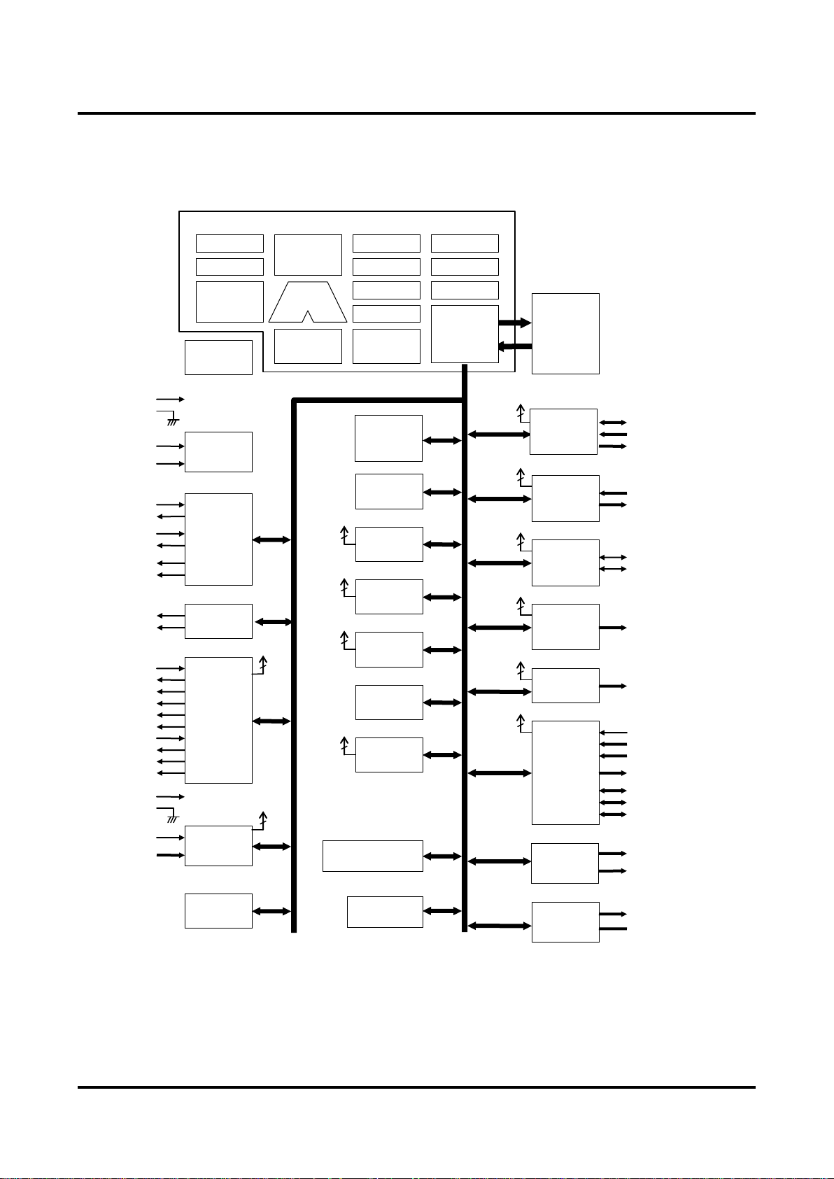
1.2.3 Block Diagram of ML610421
Program
SCK0*
SIN0*
SOUT0*
UART
RXD0*
TXD0*
I2C
SDA*
SCL*
INT
1
Interrupt
CPU (nX-U8/100)
Timing
EA
SP
On-Chip
Instruction
BUS
Instruction
TBC
INT 4 INT 1 INT 1 INT
1
WDT
INT
4
8bit Timer
Capture
INT
1
PWM
P00 to P03
P10 to P11
P20 to P22
INT 5 NMI
P30 to P35
P40 to P47
PA0 to PA7
Data-bus
PWM0*
Melody
INT 1 MD0*
TEST
RESET_N
XT0
XT1
OSC0*
OSC1*
LSCLK*
OUTCLK*
BLD
Power
AVDD
AVSS
V
DDL
LCD
COM0 to COM7
SEG0 to SEG49
LCD
VL1, VL2, VL3, VL4
C1, C2, C3, C4
12bit-ADC
AIN0, AIN1
V
REF
CS0*
IN0*
RS0*
RT0*
CRT0*
RCM*
CS1*
IN1*
RS1*
RT1*
ALU
EPSW1~3
PSW
ELR1~3
LR
ECSR1~3
DSR/CSR
PC
GREG
VDD
VSS
V
DDX
1kHzTC
INT
1
INT
1
INT
1
Display RAM
100Byte
Display Allocation
RESET &
RAM
SSIO
0~15
Controller
ICE
Decoder
TEST
OSC
RC-ADC
×2
* Secondary function or Tertiary function
Register
1024byte
Controller
×2
×4
RAM 1024Byte
ML610Q421/ML610Q422/ML610421 User’s Manual
Chapter 1 Overview
Controller
Memory
(MaskROM)
32Kbyte
GPIO
Driver
BIAS
Figure 1-3 Block Diagram of ML610421
1 – 7
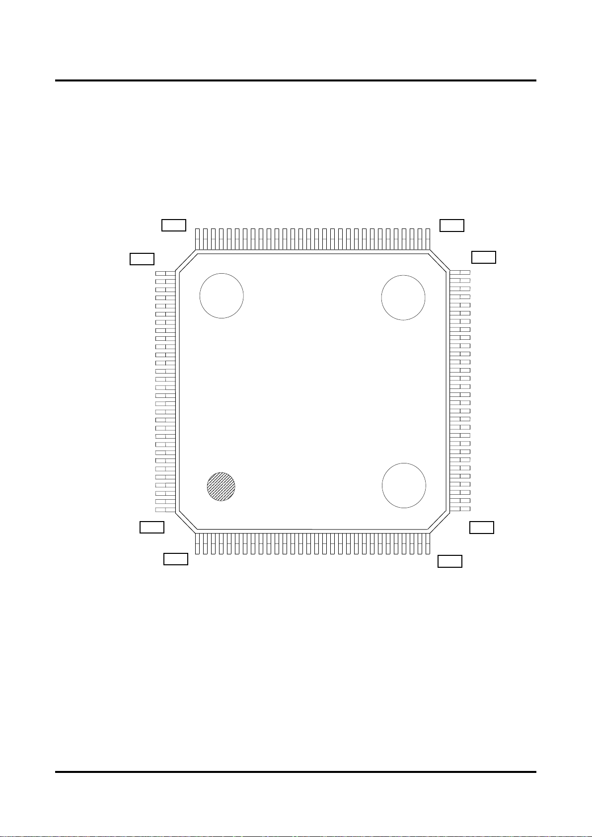
1.3 Pins
1pin
120pin
30pin
31pin
60pin
61pin
91pin
90pin
PA7
P20
P21
P22
P40
P41
VSS
PA5
PA4
PA3
PA2
PA1
PA0
COM7
COM6
COM5
COM4
COM3
COM2
COM1
COM0
SEG49
(NC)
AVSS
(NC)
VREF
AIN0
AIN1
AVDD
SEG6
SEG5
SEG4
SEG3
SEG2
SEG1
SEG0
VDD
P11
(NC)
P10
VSS
P03
P02
P01
P00
C4
C3
SEG13
SEG12
SEG11
SEG10
SEG9
SEG8
SEG7
SEG18
SEG17
SEG16
SEG15
SEG14
RESET_N
P42
P43
P44
P45
P46
P30
P31
P34
P32
P33
P35
TEST
VDD
VDDL
VSS
VDDX
XT0
VL1
VL3
VL2
NMI
VSS
XT1
VL4
C1
C2
P47
VPP*
1
(NC)
SEG41
SEG40
SEG39
SEG38
SEG37
SEG36
SEG35
SEG34
SEG33
SEG32
SEG31
SEG30
SEG29
SEG28
SEG27
SEG26
SEG25
SEG24
SEG23
SEG22
SEG21
SEG20
SEG48
SEG47
SEG46
SEG45
SEG44
SEG43
SEG42
SEG19
103
104
105
106
107
108
109
110
111
112
113
114
115
116
117
118
119
120
96
97
98
99
100
101
102
91
92
93
94
95
44
43
42
41
40
39
38
46
47
48
49
50
51
52
53
54
55
56
57
58
59
60
37
36
35
34 3332
31
8
9
10
11
12
13
14
15
16
17
18
19
20
21
22
23
24
25
26
27
28
29
1 2 3 4 5 6 7
30
89
88
87
86
85
84
82
81
80
79
78
77
76
75
74
73
72
71
66
64
65
67 68
69
63
62
61
83
90
70
1.3.1 Pin Layout
1.3.1.1 Pin Layout of ML610Q421 TQFP Package
ML610Q421/ML610Q422/ML610421 User’s Manual
Chapter 1 Overview
(NC): No Connection
Note:
The assignment of the pads P30 to P35 are not in order.
1
:A VPP terminal exists only ML610Q421.
*
Figure 1-4 Pin Layout of ML610Q421 Package
1 – 8
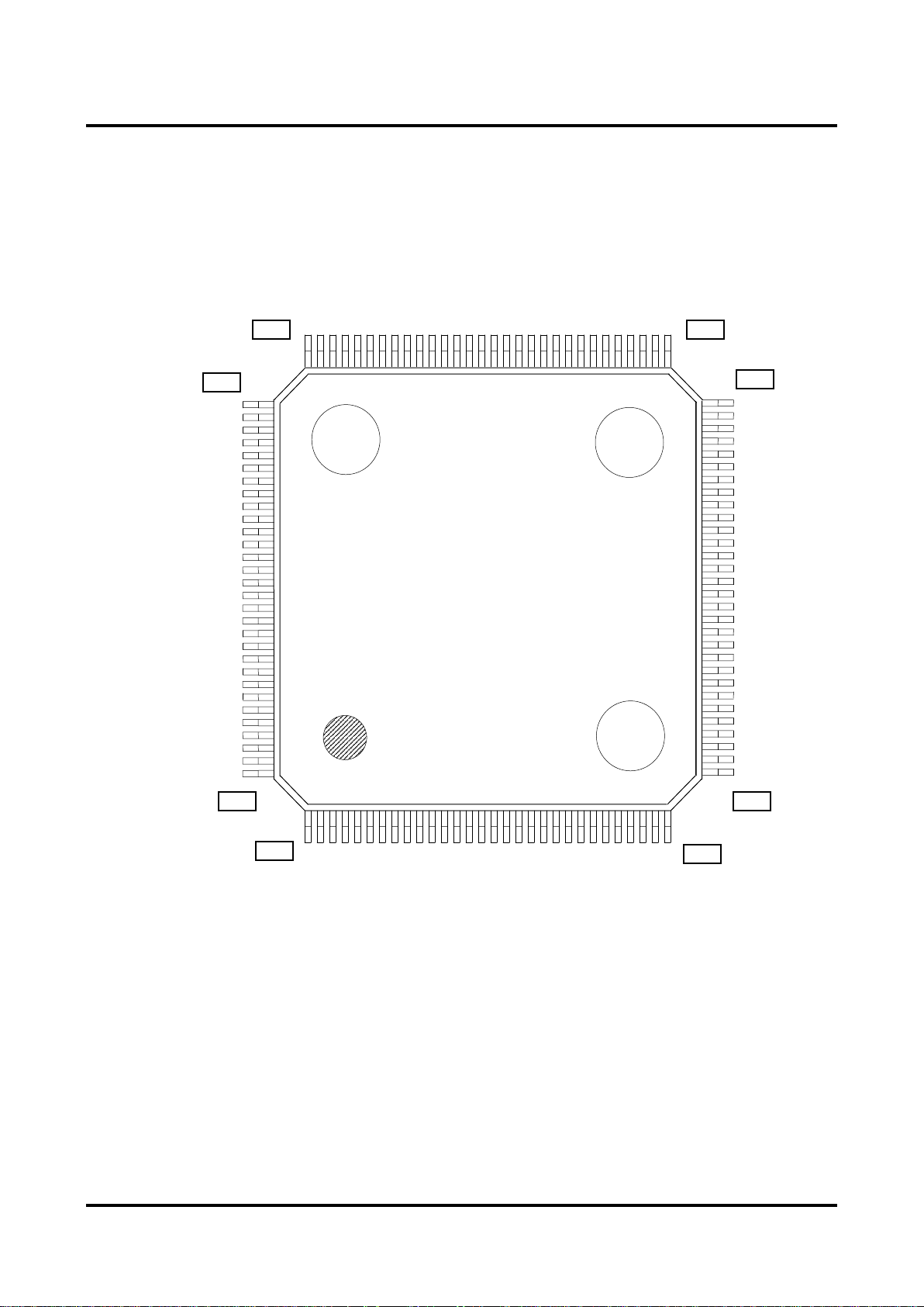
1.3.1.2 Pin Layout of ML610Q422 TQFP Package
1pin
120pin
30pin
31pin
60pin
61pin
91pin
90pin
SEG6
SEG5
SEG4
SEG3
SEG2
SEG1
SEG0
VDD
P11
(NC)
P10
VSS
P03
P02
P01
P00
C4
C3
SEG13
SEG12
SEG11
SEG10
SEG9
SEG8
SEG7
SEG18
SEG17
SEG16
SEG15
SEG14
RESET_N
P42
P43
P44
P45
P46
P30
P31
P34
P32
P33
P35
TEST
VDD
VDDL
VSS
VDDX
XT0
VL1
VL3
VL2
NMI
VSS
XT1
VL4
C1
C2
P47
VPP*
1
(NC)
SEG41
SEG40
SEG39
SEG38
SEG37
SEG36
SEG35
SEG34
SEG33
SEG32
SEG31
SEG30
SEG29
SEG28
SEG27
SEG26
SEG25
SEG24
SEG23
SEG22
SEG21
SEG20
SEG48
SEG47
SEG46
SEG45
SEG44
SEG43
SEG42
SEG19
COM15
P20
P21
P22
P40
P41
VSS
COM13
COM12
COM11
COM10
COM9
COM8
COM7
COM6
COM5
COM4
COM3
COM2
COM1
COM0
SEG49
(NC)
AVSS
(NC)
VREF
AIN0
AIN1
AVDD
103
104
105
106
107
108
109
110
111
112
113
114
115
116
117
118
119
120
96
97
98
99
100
101
102
91
92
93
94
95
8
9
10
11
12
13
14
15
16
17
18
19
20
21
22
23
24
25
26
27
28
29
1 2 3 4 5 6 7
30
44
43
42
41
40
39
38
46
47
48
49
50
51
52
53
54
55
56
57
58
59
60 3736 3534
33
32
31
89
88
87
86
85
84
82
81
80
79
78
77
76
75
74
73
72
71
66
64
65
67 68
69
63
62 61
83
90
70
ML610Q421/ML610Q422/ML610421 User’s Manual
Chapter 1 Overview
(NC): No Connection
Note:
The assignment of the pads P30 to P35 are not in order.
1
:A VPP terminal exists only ML610Q422..
*
Figure 1-5 Pin Layout of ML610Q422 Package
1 – 9
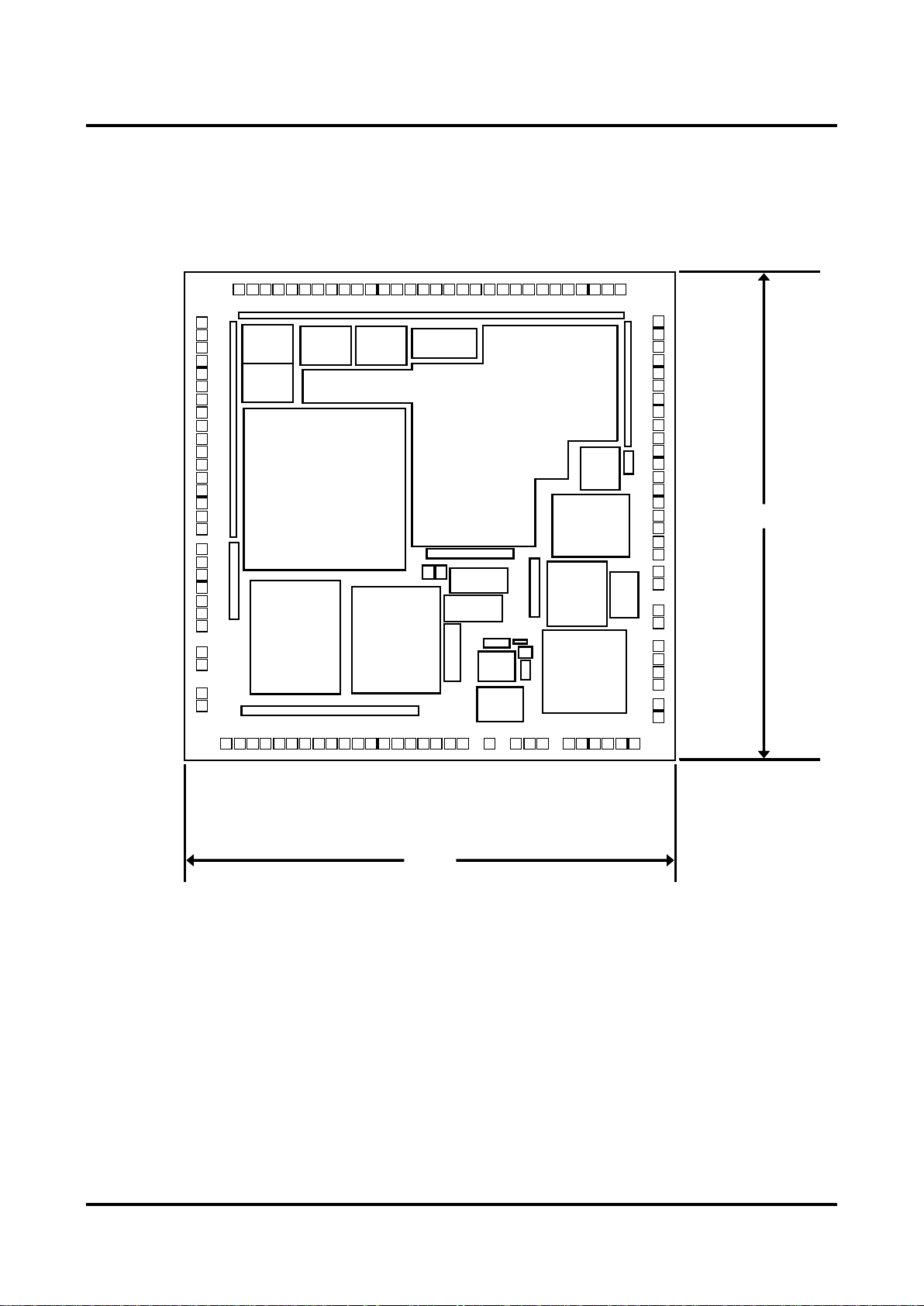
1.3.1.3 Pin Layout of ML610Q421 Chip
SEG48
SEG47
SEG46
SEG45
SEG44
SEG43
SEG42
SEG41
SEG40
SEG39
SEG38
SEG37
SEG36
SEG35
SEG34
SEG33
SEG32
SEG31
SEG30
SEG29
SEG28
SEG27
SEG26
SEG25
SEG24
SEG23
SEG22
SEG21
SEG20
SEG19
8887868584838281807978777675747372717069686766656463626160
59
SEG49 89 58 SEG18
COM0
90 57 SEG17
COM1 91 56 SEG16
COM2 92 55 SEG15
COM3 93 54 SEG14
COM4 94 53 SEG13
COM5 95 52 SEG12
COM6 96 51 SEG11
COM7 97 50 SEG10
PA0 98 49
SEG9
PA1 99 48 SEG8
PA2 100 47 SEG7
PA3 101 46 SEG6
PA4 102 45 SEG5
PA5 103 44 SEG4
PA6 104 43 SEG3
PA7 105 42 SEG2
P20/LED0 106
P21/LED1 107
P22/LED2 108
P40/SDA 109
P41/SCL 110
Vss 111
AVSS 112
VREF 113
AIN0 114
AIN1 115
AVDD 116
123456789
10111213141516171819202122232425262728
29
VPP
RESET_N
P42
P43
P44/IN1
P45/CS1
P46/RS1
P47/RT1
P30/IN0
P31/CS0
P34/RCT0
P32/RS0
P33/RT0
P35/RCM
TEST
VDD
VDDL
Vss
VDDX
XT0
XT1
Vss
NMI
VL1
VL2
VL3
VL4
C1
C2
41
40
39
38
37
363534
33
32
30
31
SEG1
SEG0
VDD
P11
P10
Vss
P03
P02
P01
P00
C3
C4
2.98mm
3.02mm
ML610Q421/ML610Q422/ML610421 User’s Manual
Chapter 1 Overview
Note:
The assignment of the pads P30 to P35 are not in order.
Chip size: 2.98 mm × 3.02mm
PAD count: 116 pins
Minimum PAD pitch: 80 µm
PAD aperture: 70 µm ×70 µm
Chip thickness: 350 µm
Voltage of the rear side of chip: V
level
SS
Figure 1-6 Dimensions of ML610Q421 Chip
1 – 10

1.3.1.4 Pin Layout of ML610Q422 Chip
SEG48
SEG47
SEG46
SEG45
SEG44
SEG43
SEG42
SEG41
SEG40
SEG39
SEG38
SEG37
SEG36
SEG35
SEG34
SEG33
SEG32
SEG31
SEG30
SEG29
SEG28
SEG27
SEG26
SEG25
SEG24
SEG23
SEG22
SEG21
SEG20
SEG19
8887868584838281807978777675747372717069686766656463626160
59
SEG49 89 58 SEG18
COM0 90 57 SEG17
COM1 91 56 SEG16
COM2 92 55 SEG15
COM3 93 54 SEG14
COM4 94 53 SEG13
COM5 95 52 SEG12
COM6 96 51 SEG11
COM7 97 50 SEG10
COM8 98 49 SEG9
COM9 99 48 SEG8
COM10 100 47 SEG7
COM11 101 46 SEG6
COM12 102 45 SEG5
COM13 103 44 SEG4
COM14 104 43 SEG3
COM15 105 42 SEG2
P20/LED0 106
P21/LED1 107
P22/LED2 108
P40/SDA 109
P41/SCL 110
Vss 111
AVSS 112
VREF 113
AIN0 114
AIN1 115
AVDD 116
123456789
10111213141516171819202122232425262728
29
VPP
RESET_N
P42
P43
P44/IN1
P45/CS1
P46/RS1
P47/RT1
P30/IN0
P31/CS0
P34/RCT0
P32/RS0
P33/RT0
P35/RCM
TEST
VDD
VDDL
Vss
VDDX
XT0
XT1
Vss
NMI
VL1
VL2
VL3
VL4
C1
C2
414039
38
37
363534
33
32
30
31
SEG1
SEG0
VDD
P11
P10
Vss
P03
P02
P01
P00
C3
C4
2.98mm
3.02mm
ML610Q421/ML610Q422/ML610421 User’s Manual
Chapter 1 Overview
Note:
The assignment of the pads P30 to P35 are not in order.
Chip size: 2.98 mm × 3.02 mm
PAD count: 116 pins
Minimum PAD pitch: 80 µm
PAD aperture: 70 µm × 70 µm
Chip thickness: 350 µm
Voltage of the rear side of chip: V
level
SS
Figure 1-7 Dimensions of ML610Q422 Chip
1 – 11
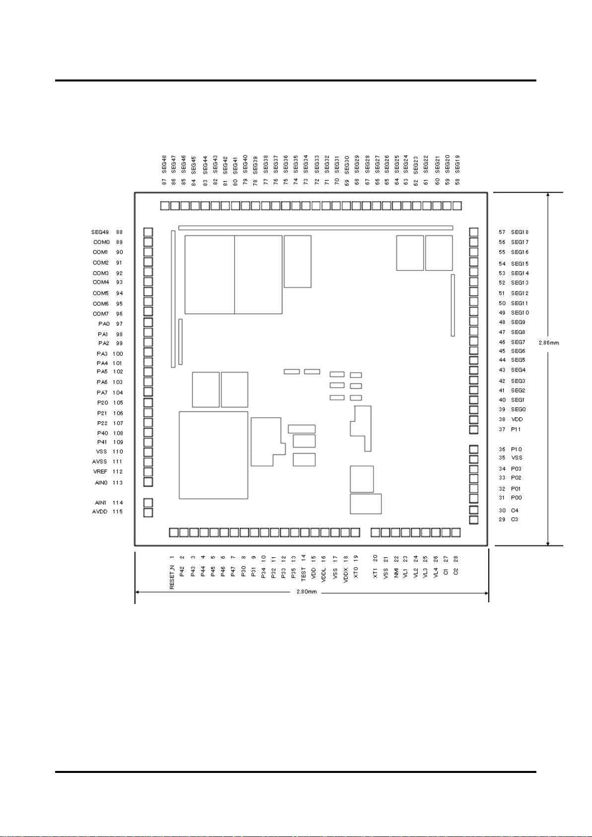
1.3.1.5 Pin Layout of ML610421 Chip
ML610Q421/ML610Q422/ML610421 User’s Manual
Chapter 1 Overview
Note:
The assignment of the pads P30 to P35 are not in order.
Chip size: 2.80 mm × 2.86mm
PAD count: 115 pins
Minimum PAD pitch: 80 µm
PAD aperture: 70 µm ×70 µm
Chip thickness: 350 µm
Voltage of the rear side of chip: V
Figure 1-8 Dimensions of ML610421 Chip
1 – 12
level
SS

1.3.1.6 Pad Coordinates of ML610Q421 Chip
Chip Center: X=0,Y=0
1
VPP
-1240
-1404 51
SEG11
1384
640 101
PA3
-1384
240 2 RESET_N
-1160
-1404 52
SEG12
1384
720 102
PA4
-1384
160 3 P42
-1080
-1404 53
SEG13
1384
800 103
PA5
-1384
80 4 P43
-1000
-1404 54
SEG14
1384
880 104
PA6
-1384 0 5
P44
-920
-1404 55
SEG15
1384
960 105
PA7
-1384
-80 6 P45
-840
-1404 56
SEG16
1384
1040 106
P20
-1384
-200 7 P46
-760
-1404 57
SEG17
1384
1120 107
P21
-1384
-280 8 P47
-680
-1404 58
SEG18
1384
1200 108
P22
-1384
-360 9 P30
-600
-1404 59
SEG19
1160
1404 109
P40
-1384
-440
10
P31
-520
-1404 60
SEG20
1080
1404 110
P41
-1384
-520
11
P34
-440
-1404 61
SEG21
1000
1404 111
Vss
-1384
-600
12
P32
-360
-1404 62
SEG22
920
1404 112
AVss
-1384
-680
13
P33
-280
-1404 63
SEG23
840
1404 113
VREF
-1384
-840
14
P35
-200
-1404 64
SEG24
760
1404 114
AIN0
-1384
-920
15
TEST
-120
-1404 65
SEG25
680
1404 115
AIN1
-1384
-1092
16
VDD
-40
-1404 66
SEG26
600
1404 116
AVDD
-1384
-1172
17
VDDL
40
-1404 67
SEG27
520
1404 18
Vss
120
-1404 68
SEG28
440
1404 19
VDDX
200
-1404 69
SEG29
360
1404 20
XT0
360
-1404 70
SEG30
280
1404 21
XT1
520
-1404 71
SEG31
200
1404 22
Vss
600
-1404 72
SEG32
120
1404 23
NMI
680
-1404 73
SEG33
40
1404 24
VL1
840
-1404 74
SEG34
-40
1404 25
VL2
920
-1404 75
SEG35
-120
1404 26
VL3
1000
-1404 76
SEG36
-200
1404 27
VL4
1080
-1404 77
SEG37
-280
1404 28
C1
1160
-1404 78
SEG38
-360
1404 29
C2
1240
-1404 79
SEG39
-440
1404 30
C3
1384
-1240 80
SEG40
-520
1404 31
C4
1384
-1160 81
SEG41
-600
1404 32
P00
1384
-1040 82
SEG42
-680
1404 33
P01
1384
-960 83
SEG43
-760
1404 34
P02
1384
-880 84
SEG44
-840
1404 35
P03
1384
-800 85
SEG45
-920
1404 36
Vss
1384
-660 86
SEG46
-1000
1404 37
P10
1384
-580 87
SEG47
-1080
1404 38
P11
1384
-420 88
SEG48
-1160
1404 39
VDD
1384
-340 89
SEG49
-1384
1200 40
SEG0
1384
-240 90
COM0
-1384
1120 41
SEG1
1384
-160 91
COM1
-1384
1040 42
SEG2
1384
-80 92
COM2
-1384
960 43
SEG3
1384
0 93
COM3
-1384
880 44
SEG4
1384
80 94
COM4
-1384
800 45
SEG5
1384
160 95
COM5
-1384
720 46
SEG6
1384
240 96
COM6
-1384
640 47
SEG7
1384
320 97
COM7
-1384
560 48
SEG8
1384
400 98
PA0
-1384
480 49
SEG9
1384
480 99
PA1
-1384
400 50
SEG10
1384
560 100
PA2
-1384
320
Table 1-1 Pad Coordinates of ML610Q421
ML610Q421/ML610Q422/ML610421 User’s Manual
Chapter 1 Overview
PAD
No.
Pad
Name X (μm) Y (μm)
PAD
No.
Pad
Name X (μm) Y (μm)
PAD
No.
Pad
Name X (μm) Y (μm)
1 – 13
1.3.1.7 Pad Coordinates of ML610Q422 Chip
Chip Center: X=0,Y=0
1
VPP
-1240
-1404 51
SEG11
1384
640 101
COM11
-1384
240 2 RESET_N
-1160
-1404 52
SEG12
1384
720 102
COM12
-1384
160 3 P42
-1080
-1404 53
SEG13
1384
800 103
COM13
-1384
80 4 P43
-1000
-1404 54
SEG14
1384
880 104
COM14
-1384 0 5
P44
-920
-1404 55
SEG15
1384
960 105
COM15
-1384
-80 6 P45
-840
-1404 56
SEG16
1384
1040 106
P20
-1384
-200 7 P46
-760
-1404 57
SEG17
1384
1120 107
P21
-1384
-280 8 P47
-680
-1404 58
SEG18
1384
1200 108
P22
-1384
-360 9 P30
-600
-1404 59
SEG19
1160
1404 109
P40
-1384
-440
10
P31
-520
-1404 60
SEG20
1080
1404 110
P41
-1384
-520
11
P34
-440
-1404 61
SEG21
1000
1404 111
Vss
-1384
-600
12
P32
-360
-1404 62
SEG22
920
1404 112
AVss
-1384
-680
13
P33
-280
-1404 63
SEG23
840
1404 113
VREF
-1384
-840
14
P35
-200
-1404 64
SEG24
760
1404 114
AIN0
-1384
-920
15
TEST
-120
-1404 65
SEG25
680
1404 115
AIN1
-1384
-1092
16
VDD
-40
-1404 66
SEG26
600
1404 116
AVDD
-1384
-1172
17
VDDL
40
-1404 67
SEG27
520
1404 18
Vss
120
-1404 68
SEG28
440
1404 19
VDDX
200
-1404 69
SEG29
360
1404 20
XT0
360
-1404 70
SEG30
280
1404 21
XT1
520
-1404 71
SEG31
200
1404 22
Vss
600
-1404 72
SEG32
120
1404 23
NMI
680
-1404 73
SEG33
40
1404 24
VL1
840
-1404 74
SEG34
-40
1404 25
VL2
920
-1404 75
SEG35
-120
1404 26
VL3
1000
-1404 76
SEG36
-200
1404 27
VL4
1080
-1404 77
SEG37
-280
1404 28
C1
1160
-1404 78
SEG38
-360
1404 29
C2
1240
-1404 79
SEG39
-440
1404 30
C3
1384
-1240 80
SEG40
-520
1404 31
C4
1384
-1160 81
SEG41
-600
1404 32
P00
1384
-1040 82
SEG42
-680
1404 33
P01
1384
-960 83
SEG43
-760
1404 34
P02
1384
-880 84
SEG44
-840
1404 35
P03
1384
-800 85
SEG45
-920
1404 36
Vss
1384
-660 86
SEG46
-1000
1404 37
P10
1384
-580 87
SEG47
-1080
1404 38
P11
1384
-420 88
SEG48
-1160
1404 39
VDD
1384
-340 89
SEG49
-1384
1200 40
SEG0
1384
-240 90
COM0
-1384
1120 41
SEG1
1384
-160 91
COM1
-1384
1040 42
SEG2
1384
-80 92
COM2
-1384
960 43
SEG3
1384
0 93
COM3
-1384
880 44
SEG4
1384
80 94
COM4
-1384
800 45
SEG5
1384
160 95
COM5
-1384
720 46
SEG6
1384
240 96
COM6
-1384
640 47
SEG7
1384
320 97
COM7
-1384
560 48
SEG8
1384
400 98
COM8
-1384
480 49
SEG9
1384
480 99
COM9
-1384
400 50
SEG10
1384
560 100
COM10
-1384
320
Table 1-2 Pad Coordinates of ML610Q422
ML610Q421/ML610Q422/ML610421 User’s Manual
Chapter 1 Overview
PAD
No.
Pad
Name X (μm) Y (μm)
PAD
No.
Pad
Name X (μm) Y (μm)
PAD
No.
Pad
Name X (μm) Y (μm)
1 – 14
1.3.1.8 Pad Coordinates of ML610421 Chip
Chip Center: X=0,Y=0
1
RESET_N
-1090
-1324 51
SEG12
1294
630 101
PA4
-1294
60 2 P42
-1010
-1324 52
SEG13
1294
710 102
PA5
-1294
-20 3 P43
-930
-1324 53
SEG14
1294
790 103
PA6
-1294
-100 4 P44
-850
-1324 54
SEG15
1294
870 104
PA7
-1294
-180 5 P45
-770
-1324 55
SEG16
1294
950 105
P20
-1294
-270 6 P46
-690
-1324 56
SEG17
1294
1030 106
P21
-1294
-350 7 P47
-610
-1324 57
SEG18
1294
1110 107
P22
-1294
-430 8 P30
-530
-1324 58
SEG19
1160
1324 108
P40
-1294
-510 9 P31
-450
-1324 59
SEG20
1080
1324 109
P41
-1294
-590
10
P34
-370
-1324 60
SEG21
1000
1324 110
Vss
-1294
-670
11
P32
-290
-1324 61
SEG22
920
1324 111
AVss
-1294
-750
12
P33
-210
-1324 62
SEG23
840
1324 112
VREF
-1294
-830
13
P35
-130
-1324 63
SEG24
760
1324 113
AIN0
-1294
-910
14
TEST
-50
-1324 64
SEG25
680
1324 114
AIN1
-1294
-1082
15
VDD
30
-1324 65
SEG26
600
1324 115
AVDD
-1294
-1162
16
VDDL
110
-1324 66
SEG27
520
1324 17
Vss
190
-1324 67
SEG28
440
1324 18
VDDX
270
-1324 68
SEG29
360
1324 19
XT0
350
-1324 69
SEG30
280
1324 20
XT1
510
-1324 70
SEG31
200
1324 21
Vss
590
-1324 71
SEG32
120
1324 22
NMI
670
-1324 72
SEG33
40
1324 23
VL1
750
-1324 73
SEG34
-40
1324 24
VL2
830
-1324 74
SEG35
-120
1324 25
VL3
910
-1324 75
SEG36
-200
1324 26
VL4
990
-1324 76
SEG37
-280
1324 27
C1
1070
-1324 77
SEG38
-360
1324 28
C2
1150
-1324 78
SEG39
-440
1324 29
C3
1294
-1220 79
SEG40
-520
1324 30
C4
1294
-1140 80
SEG41
-600
1324 31
P00
1294
-1050 81
SEG42
-680
1324 32
P01
1294
-970 82
SEG43
-760
1324 33
P02
1294
-890 83
SEG44
-840
1324 34
P03
1294
-810 84
SEG45
-920
1324 35
Vss
1294
-730 85
SEG46
-1000
1324 36
P10
1294
-650 86
SEG47
-1080
1324 37
P11
1294
-490 87
SEG48
-1160
1324 38
VDD
1294
-410 88
SEG49
-1294
1110 39
SEG0
1294
-330 89
COM0
-1294
1030 40
SEG1
1294
-250 90
COM1
-1294
950 41
SEG2
1294
-170 91
COM2
-1294
870 42
SEG3
1294
-90 92
COM3
-1294
790 43
SEG4
1294
-10 93
COM4
-1294
710 44
SEG5
1294
70 94
COM5
-1294
630 45
SEG6
1294
150 95
COM6
-1294
550 46
SEG7
1294
230 96
COM7
-1294
470 47
SEG8
1294
310 97
PA0
-1294
380 48
SEG9
1294
390 98
PA1
-1294
300 49
SEG10
1294
470 99
PA2
-1294
220 50
SEG11
1294
550 100
PA3
-1294
140
Table 1-3 Pad Coordinates of ML610421
ML610Q421/ML610Q422/ML610421 User’s Manual
Chapter 1 Overview
PAD
No.
Pad
Name X (μm) Y (μm)
PAD
No.
Pad
Name X (μm) Y (μm)
PAD
No.
Pad
Name X (μm) Y (μm)
1 – 15

1.3.2 List of Pins
PAD No.
Primary function
Secondary function
Tertiary function
Q422
Q421
Pin name
I/O
Function
Pin name
I/O
Function
Pin name
I/O
Function
36,111
36,111
Positive power supply
pin
Power supply pin for
(internally generated)
Power supply pin for
(internally generated)
Power supply pin for
Flash ROM
Negative power
ADC
Positive power supply
ADC
Power supply pin for
generated)
Power supply pin for
generated)
Power supply pin for
generated)
Power supply pin for
generated)
Capacitor connection
generation
Capacitor connection
generation
Capacitor connection
generation
Capacitor connection
generation
Input/output pin for
testing
N
Low-speed clock
oscillation pin
Low-speed clock
oscillation pin
Reference power
ADC
1.3.2.1 List of ML610Q421/ML610Q422 Pins
18,22,
18,22,
Vss
Negative power
supply pin
ML610Q421/ML610Q422/ML610421 User’s Manual
Chapter 1 Overview
16,39 16,39 VDD
17 17 V
19 19 V
1 1 VPP
112 112 AVSS
116 116 AVDD
24 24 VL1
25 25 VL2
26 26 VL3
27 27 VL4
DDL
DDX
internal logic
low-speed oscillation
supply pin for
successive
approximation type
pin for successive
approximation type
LCD bias (internally
LCD bias (internally
LCD bias (internally
LCD bias (internally
28 28 C1
29 29 C2
30 30 C3
31 31 C4
15 15 TEST I/O
2 2
20 20 XT0 I
21 21 XT1 O
113 113 V
RESET_
REF
pin for LCD bias
pin for LCD bias
pin for LCD bias
pin for LCD bias
Reset input pin
I
supply pin for
successive
approximation type
1 – 16

ML610Q421/ML610Q422/ML610421 User’s Manual
Q422
Q421
Pin name
I/O
Function
Pin name
I/O
Function
Pin name
I/O
Function
Successive
ADC input
Successive
ADC input
Non-maskable
interrupt pin
Input port, External
input
Input port, External
input
Input port, External
receive
3
37
37
P10
I
Input port
OSC0
I
High-speed oscillation
38
38
P11
I
Input port
OSC1
O
High-speed oscillation
D0
speed clock output
1
D2
RC type ADC0
oscillation input pin
RC type ADC0
sensor connection pin
RC type ADC0
connection pin
RC type ADC0 resistor
sensor connection pin
RC type ADC
oscillation moni t or
109
109
P40
I/O
SDA
I/O
SIN0
I
SSIO synchronous
clock
3 3 P42
I/O
RXD0
I
SOUT0
O
4 4 P43
I/O
Input/output port
TXD0
O
UART data output
PWM0
O
PWM output
Input/output port,
clock input
Input/output port,
external clock input
RC type ADC1
connection pin
RC type ADC1
connection pin
RC type ADC1 resistor
sensor connection pin
98
PA0
I/O
Input/output port
Chapter 1 Overview
PAD No. Primary function Secondary function Tertiary function
114 114 AIN0 I
115 115 AIN1 I
23 23 NMI I
32 32
33 33
34 34
35 35
106 106
107 107
108 108
P00/EXI
0/CAP0
P01/EXI
1/CAP1
P02/EXI
2/RXD0
P03/EXI
P20/LE
P21LED
P22/LE
approximation type
approximation type
interrupt 0, Capture 0
I
interrupt 1, Capture 1
I
interrupt 2, UART0
I
Input port, External
I
interrupt 3
Output port
O
Output port
O
Output port
O
LSCLK O
OUTCLK O
MD0 O
LowHigh-speed clock
output
Melody output
9 9 P30 I/O
10 10 P31 I/O
11 11 P34 I/O
12 12 P32 I/O
13 13 P33 I/O
14 14 P35 I/O
110 110 P41 I/O
5 5
6 6
P44/T02
P0CK
P45/T13
P1CK
I/O
I/O
Input/output port
Input/output port
Input/output port
Input/output port
Input/output port
Input/output port
Input/output port
Input/output port
Input/output port
Timer 0/Timer
2/PWM0 external
Timer 1/Timer 3
IN0 I
CS0 O
RCT0 O
RS0 O
RT0 O
RCM O
SCL I/O
IN1 I
CS1 O
RC type ADC0
reference capacitor
connection pin
resistor/capacitor
reference resistor
I2C data input/output
2
I
C clock input/output
UART data input
RC type ADC1
oscillation input pin
reference capacitor
PWM0 O
SCK0 I/O
SIN0 I
SCK0 I/O
PWM output
SSIO data input
SSIO data output
SSIO0 data input
SSIO0 synchronous
clock
7 7 P46 I/O
8 8 P47 I/O
Input/output port
Input/output port
RS1 O
RT1 O
1 – 17
reference resistor
SOUT0 O
SSIO0 data output

ML610Q421/ML610Q422/ML610421 User’s Manual
Q422
Q421
Pin name
I/O
Function
Pin name
I/O
Function
Pin name
I/O
Function
99
PA1
I/O
Input/output port
100
PA2
I/O
Input/output port
101
PA3
I/O
Input/output port
102
PA4
I/O
Input/output port
103
PA5
I/O
Input/output port
104
PA6
I/O
Input/output port
105
PA7
I/O
Input/output port
90
90
COM0
O
LCD common pin
91
91
COM1
O
LCD common pin
92
92
COM2
O
93
93
COM3
O
LCD common pin
94
94
COM4
O
LCD common pin
95
95
COM5
O
LCD common pin
96
96
COM6
O
LCD common pin
97
97
COM7
O
LCD common pin
98 COM8
O
LCD common pin
99 COM9
O
LCD common pin
100 COM10
O
LCD common pin
101 COM11
O
LCD common pin
102
COM12
O
LCD common pin
103
COM13
O
LCD common pin
104
COM14
O
LCD common pin
105
COM15
O
LCD common pin
40
40
SEG0
O
LCD segment pin
41
41
SEG1
O
LCD segment pin
42
42
SEG2
O
43
43
SEG3
O
44
44
SEG4
O
45
45
SEG5
O
46
46
SEG6
O
47
47
SEG7
O
48
48
SEG8
O
49
49
SEG9
O
LCD segment pin
50
50
SEG10
O
LCD segment pin
51
51
SEG11
O
52
52
SEG12
O
LCD segment pin
53
53
SEG13
O
LCD segment pin
54
54
SEG14
O
LCD segment pin
55
55
SEG15
O
LCD segment pin
56
56
SEG16
O
LCD segment pin
57
57
SEG17
O
LCD segment pin
58
58
SEG18
O
LCD segment pin
59
59
SEG19
O
LCD segment pin
60
60
SEG20
O
LCD segment pin
61
61
SEG21
O
LCD segment pin
62
62
SEG22
O
LCD segment pin
63
63
SEG23
O
LCD segment pin
64
64
SEG24
O
LCD segment pin
65
65
SEG25
O
LCD segment pin
66
66
SEG26
O
LCD segment pin
Chapter 1 Overview
PAD No. Primary function Secondary function Tertiary function
LCD common pin
LCD segment pin
LCD segment pin
LCD segment pin
LCD segment pin
LCD segment pin
LCD segment pin
LCD segment pin
LCD segment pin
1 – 18
ML610Q421/ML610Q422/ML610421 User’s Manual
Q422
Q421
Pin name
I/O
Function
Pin name
I/O
Function
Pin name
I/O
Function
67
67
SEG27
O
68
68
SEG28
O
69
69
SEG29
O
70
70
SEG30
O
71
71
SEG31
O
72
72
SEG32
O
LCD segment pin
73
73
SEG33
O
LCD segment pin
74
74
SEG34
O
LCD segment pin
75
75
SEG35
O
LCD segment pin
76
76
SEG36
O
LCD segment pin
77
77
SEG37
O
LCD segment pin
78
78
SEG38
O
LCD segment pin
79
79
SEG39
O
LCD segment pin
80
80
SEG40
O
LCD segment pin
81
81
SEG41
O
LCD segment pin
82
82
SEG42
O
LCD segment pin
83
83
SEG43
O
LCD segment pin
84
84
SEG44
O
LCD segment pin
85
85
SEG45
O
LCD segment pin
86
86
SEG46
O
LCD segment pin
87
87
SEG47
O
LCD segment pin
88
88
SEG48
O
LCD segment pin
89
89
SEG49
O
LCD segment pin
Chapter 1 Overview
PAD No. Primary function Secondary function Tertiary function
LCD segment pin
LCD segment pin
LCD segment pin
LCD segment pin
LCD segment pin
1 – 19

PAD No.
Primary function
Secondary function
Tertiary function
421
Pin name
I/O
Function
Pin name
I/O
Function
Pin name
I/O
Function
35,110
Negative power supply
Positive power supply
pin
Power supply pin for
internally
generated)
Power supply pin for
(internally generated)
Negative power supply
ADC
Positive power supply
ADC
Power supply pin for
generated)
Power supply pin for
generated)
Power supply pin for
generated)
Power supply pin for
generated)
Capacitor connection
generation
Capacitor connection
generation
Capacitor connection
generation
Capacitor connection
generation
14
TEST
I
N
Low-speed clock
oscillation pin
Low-speed clock
oscillation pin
Reference power
ADC
Successive
ADC input
Successive
ADC input
1.3.2.2 List of ML610421 Pins
ML610Q421/ML610Q422/ML610421 User’s Manual
Chapter 1 Overview
17,21,
15,38 VDD
16 V
18 V
111 AVSS
115 AVDD
23 VL1
24 VL2
25 VL3
26 VL4
Vss
DDL
DDX
pin
internal logic (
low-speed oscillation
pin for successive
approximation type
pin for successive
approximation type
LCD bias (internally
LCD bias (internally
LCD bias (internally
LCD bias (internally
27 C1
28 C2
29 C3
30 C4
1
19 XT0 I
20 XT1 O
112 V
113 AIN0 I
114 AIN1 I
RESET_
REF
pin for LCD bias
pin for LCD bias
pin for LCD bias
pin for LCD bias
Input pin for testing
Reset input pin
I
supply pin for
successive
approximation type
approximation type
approximation type
1 – 20

ML610Q421/ML610Q422/ML610421 User’s Manual
421
Pin name
I/O
Function
Pin name
I/O
Function
Pin name
I/O
Function
Non-maskable
interrupt pin
Input port, External
input
Input port, External
input
Input port, External
receive
3
High-speed
oscillation
High-speed
oscillation
0
1
2
RC type ADC0
pin
RC type ADC0
connection pin
RC type ADC0
pin
RC type ADC0
connection pin
RC type ADC0
connection pin
RC type ADC
oscillation moni t or
I2C data
input/output
I2C clock
input/output
SSIO synchronous
clock
2
P42
I/O
Input/output port
RXD0
I
UART data input
SOUT0
O
SSIO data output
3
P43
I/O
Input/output port
TXD0
O
UART data output
PWM0
O
PWM output
Input/output port,
clock input
RC type ADC1
connection pin
RC type ADC1
connection pin
RC type ADC1
resistor sensor
Chapter 1 Overview
PAD No. Primary function Secondary function Tertiary function
22 NMI I
31
32
33
34
36 P10 I
37 P11 I
105
106
107
8 P30 I/O
9 P31 I/O
P00/EXI
0/CAP0
P01/EXI
1/CAP1
P02/EXI
2/RXD0
P03/EXI
P20/LED
P21LED
P22/LED
interrupt 0, Capture 0
I
interrupt 1, Capture 1
I
interrupt 2, UART0
I
Input port, External
I
interrupt 3
Input port
Input port
Output port
O
Output port
O
Output port
O
Input/output port
Input/output port
OSC0 I
OSC1 O
LSCLK O
OUTCLK O
MD0 O
IN0 I
CS0 O
Low-speed clock
output
High-speed clock
output
Melody output
oscillation input
reference
capacitor
10 P34 I/O
11 P32 I/O
12 P33 I/O
13 P35 I/O
108 P40 I/O
109 P41 I/O
4
5
6 P46 I/O
P44/T02
P0CK
P45/T13
P1CK
I/O
I/O
Input/output port
Input/output port
Input/output port
Input/output port
Input/output port
Input/output port
Timer 0/Timer
2/PWM0 external
Input/output port,
Timer 1/Timer 3
external clock input
Input/output port
RCT0 O
RS0 O
RT0 O
RCM O
SDA I/O
SCL I/O
IN1 I
CS1 O
RS1 O
resistor/capacitor
sensor connection
reference resistor
resistor sensor
RC type ADC1
oscillation input
pin
reference
capacitor
reference resistor
PWM0 O
SIN0 I
SCK0 I/O
SIN0 I
SCK0 I/O
SOUT0 O
PWM output
SSIO data input
SSIO0 data input
SSIO0
synchronous clock
SSIO0 data output
7 P47 I/O
Input/output port
RT1 O
1 – 21

ML610Q421/ML610Q422/ML610421 User’s Manual
421
Pin name
I/O
Function
Pin name
I/O
Function
Pin name
I/O
Function
connection pin
97
PA0
I/O
Input/output port
98
PA1
I/O
Input/output port
99
PA2
I/O
Input/output port
100
PA3
I/O
Input/output port
101
PA4
I/O
Input/output port
102
PA5
I/O
Input/output port
103
PA6
I/O
Input/output port
104
PA7
I/O
Input/output port
89
COM0
O
LCD common pin
90
COM1
O
LCD common pin
91
COM2
O
LCD common pin
92
COM3
O
LCD common pin
93
COM4
O
LCD common pin
94
COM5
O
LCD common pin
95
COM6
O
LCD common pin
96
COM7
O
LCD common pin
COM8
O
LCD common pin
COM9
O
LCD common pin
COM10
O
LCD common pin
COM11
O
LCD common pin
COM12
O
LCD common pin
COM13
O
LCD common pin
COM14
O
LCD common pin
COM15
O
LCD common pin
39
SEG0
O
40
SEG1
O
41
SEG2
O
42
SEG3
O
43
SEG4
O
44
SEG5
O
45
SEG6
O
46
SEG7
O
LCD segment pin
47
SEG8
O
LCD segment pin
48
SEG9
O
LCD segment pin
49
SEG10
O
LCD segment pin
50
SEG11
O
LCD segment pin
51
SEG12
O
LCD segment pin
52
SEG13
O
LCD segment pin
53
SEG14
O
LCD segment pin
54
SEG15
O
LCD segment pin
55
SEG16
O
LCD segment pin
56
SEG17
O
LCD segment pin
57
SEG18
O
LCD segment pin
58
SEG19
O
LCD segment pin
59
SEG20
O
LCD segment pin
60
SEG21
O
LCD segment pin
61
SEG22
O
LCD segment pin
62
SEG23
O
LCD segment pin
63
SEG24
O
LCD segment pin
Chapter 1 Overview
PAD No. Primary function Secondary function Tertiary function
LCD segment pin
LCD segment pin
LCD segment pin
LCD segment pin
LCD segment pin
LCD segment pin
LCD segment pin
1 – 22

ML610Q421/ML610Q422/ML610421 User’s Manual
421
Pin name
I/O
Function
Pin name
I/O
Function
Pin name
I/O
Function
64
SEG25
O
65
SEG26
O
66
SEG27
O
67
SEG28
O
68
SEG29
O
69
SEG30
O
LCD segment pin
70
SEG31
O
LCD segment pin
71
SEG32
O
LCD segment pin
72
SEG33
O
LCD segment pin
73
SEG34
O
LCD segment pin
74
SEG35
O
LCD segment pin
75
SEG36
O
LCD segment pin
76
SEG37
O
LCD segment pin
77
SEG38
O
LCD segment pin
78
SEG39
O
LCD segment pin
79
SEG40
O
LCD segment pin
80
SEG41
O
LCD segment pin
81
SEG42
O
LCD segment pin
82
SEG43
O
LCD segment pin
83
SEG44
O
LCD segment pin
84
SEG45
O
LCD segment pin
85
SEG46
O
LCD segment pin
86
SEG47
O
LCD segment pin
87
SEG48
O
88
SEG49
O
Chapter 1 Overview
PAD No. Primary function Secondary function Tertiary function
LCD segment pin
LCD segment pin
LCD segment pin
LCD segment pin
LCD segment pin
LCD segment pin
LCD segment pin
1 – 23
1.3.3 Description of Pins
Primary/
econdary/
Tertiary
System
Reset input pin. When this pin is set to a “L” level, system reset mode is
connected.
XT0
I
Crystal connection pin for low-speed clock.
as required.
—
—
OSC0
I
Crystal/ceramic connection pin for high-speed clock.
pin(OSC1).
Secondary
—
OSC1
O
Secondary
—
Low-speed clock output pin. This pin is used as the secondary function of
the P20 pin.
OUTCLK
O
High-speed clock output pin. This pin is used as the secondary function
of the P21 pin.
Secondary
—
General-purpose input port
General-purpose input port.
port when the secondary functions are used.
P10-P11
I
General-purpose input port.
port when the secondary functions are used.
Primary
Positive
General-purpose output port
P20-P22
O
General-purpose output port.
port when the secondary functions are used.
Primary
Positive
General-purpose input/output port
General-purpose input/output port.
port when the secondary functions are used.
P40-P47
I/O
General-purpose input/output port.
port when the secondary functions are used.
Primary
Positive
General-purpose input/output port.
ML610Q421/ML610Q422/ML610421 User’s Manual
Chapter 1 Overview
Pin name I/O Description
RESET_N I
set and the internal section is initialized. When this pin is set to a “H” level
subsequently, program execution starts. A pull-up resistor is internally
XT1 O
LSCLK O
P00-P03 I
A 32.768 kHz crystal oscillator (see measuring circuit 1) is connected to
this pin. Capacitors CDL and CGL are connected across this pin and V
A crystal or ceramic is connected to this pin (4.1 MHz max.). Capacitors
CDH and CGH (see measuring circuit 1) are connected across this pin
and V
This pin is used as the secondary function of the P10 pin(OSC0) and P11
Since these pins have secondary functions, the pins cannot be used as a
.
SS
S
— Negative
SS
— —
Secondary —
Primary Positive
Logic
P30-P35 I/O
PA0-PA7 I/O
Since these pins have secondary functions, the pins cannot be used as a
Since these pins have secondary functions, the pins cannot be used as a
Primary Positive
Since these pins have secondary functions, the pins cannot be used as a
Since these pins have secondary functions, the pins cannot be used as a
Primary Positive
These pins are for the ML610Q421/ML610421, but are not provided in
the ML610Q422.
1 – 24

ML610Q421/ML610Q422/ML610421 User’s Manual
Primary/
Secondary/
Tertiary
UART
UART data output pin. This pin is used as the secondary function of the
P43 pin.
RXD0
I
UART data input pin. This pin is used as the secondary function of the
Primary/Se
condary
Positive
I2C bus interface
I2C data input/output pin. This pin is used as the secondary function of
pin as a function of the I2C, externally connect a pull-up resistor.
SCL
I/O
I2C clock input/output pin. This pin is used as the secondary function of
pin as a function of the I2C, externally connect a pull-up resistor.
Secondary
Positive
Synchronous serial (SSIO)
Synchronous serial clock input/output pin. This pin is used as the tertiary
function of the P41 or P45 pin.
SIN0
I
Synchronous serial data input pin. This pin is used as the tertiary function
of the P40 or P44 pin.
Tertiary
Positive
SOUT0
O
Synchronous serial data output pin. This pin is used as the tertiary
function of the P42 or P46 pin.
Tertiary
Positive
PWM
PWM0
O
PWM0 output pin. This pin is used as the tertiary function of the P43 or
P34 pin.
Tertiary
Positive
PWM0 external clock input pin. This pin is used as the primary function of
the P44 pin.
External interrupt
External non-maskable interrupt input pin. An interrupt is generated on
both edges.
Positive/
negative
EXI0-3
I
External maskable interrupt input pins. Interrupt enable and edge
as the primary functions of the P00-P03 pins.
Primary
Positive/
Capture
Capture trigger input pins. The value of the time base counter is captured
P01 pin(CAP1).
Positive/
negative
CAP1
I
Primary
Positive/
negative
Timer
External clock input pin used for both Timer 0 and Timer 2. The clocks for
function of the P44 pin.
T13P1CK
I
External clock input pin used for both Timer 1 and Timer 3. The clocks for
function of the P45 pin.
Primary
Melody
MD0
O
Melody/buzzer signal output pin. This pin is used as the secondary
function of the P22 pin.
Secondary
Positive/
negative
LED drive
Nch open drain output pins to drive LED.
Positive/
negative
Chapter 1 Overview
Pin name I/O Description
TXD0 O
P42 or the primary function of the P02 pin.
SDA I/O
the P40 pin. This pin has an NMOS open drain output. When using this
the P41 pin. This pin has an NMOS open drain output. When using this
SCK0 I/O
T02P0CK O
Logic
Secondary Positive
Secondary Positive
Tertiary —
Primary —
NMI I
CAP0 I
T02P0CK I
LED0-2 O
selection can be performed for each bit by software. These pins are used
in the register synchronously with the interrupt edge selected by software.
These pins are used as the primary functions of the P00 pin(CAP0) and
these timers are selected by software. This pin is used as the primary
these timers are selected by software. This pin is used as the primary
Primary
negative
Primary
Primary
—
—
Primary
1 – 25

ML610Q421/ML610Q422/ML610421 User’s Manual
Primary/
Secondary/
Tertiary
RC oscillation type A/D converter
Channel 0 oscillation input pin. This pin is used as the secondary function
of the P30 pin.
CS0
O
Channel 0 reference capacitor connection pin. This pin is used as the
secondary function of the P31 pin.
Secondary
This pin is used as the secondary function of the P32 pin which is the
reference resistor connection pin of Channel 0.
Resistor sensor connection pin of Channel 0 for measurement. This pin is
used as the secondary function of the P33 pin.
RCT0
O
Resistor/capacitor sensor connection pin of Channel 0 for measurement.
This pin is used as the secondary function of the P34 pin.
Secondary
RC oscillation monitor pin. This pin is used as the secondary function of
the P35 pin.
IN1
I
Oscillation input pin of Channel 1. This pin is used as the secondary
function of the P44 pin.
Secondary
Reference capacitor connection pin of Channel 1. This pin is used as the
secondary function of the P45 pin.
RS1
O
Reference resistor connection pin of Channel 1. This pin is used as the
secondary function of the P46 pin.
Secondary
Resistor sensor connection pin for measurement of Channel 1. This pin is
used as the secondary function of the P47 pin.
Successive approximation type A/D converter
AVSS
—
Negative power supply pin for successive approximation type A/D
converter.
—
—
Positive power supply pin for successive approximation type A/D
converter.
V
—
Reference power supply pin for successive approximation type A/D
converter.
—
—
AIN0
I
Channel 0 analog input for successive approximation type A/D converter.
— — AIN1
I
Channel 1 analog input for successive approximation type A/D converter.
—
—
LCD drive signal
COM0-7
O
Common output pins.
—
—
Common output pins.
ML610Q421/ML610421.
SEG0-49
O
Segment output pin.
—
—
LCD driver power supply
VL1
—
Power supply pins for LCD bias (internally generated). Capacitors Ca, Cb,
— — VL2 — — — VL3 — — — VL4 — — — C1
—
Power supply pins for LCD bias (internally generated). Capacitors C12
— — C2 — — — C3 — — — C4 — —
—
For testing
TEST
I/O
ML610Q421/ML610Q422:Input/output pin for testing.
connected
—
—
Power supply
VSS
—
Negative power supply pin.
— — VDD
—
Positive power supply pin.
—
—
Chapter 1 Overview
Pin name I/O Description
IN0 I
RS0 O
RT0 O
RCM O
CS1 O
RT1 O
Secondary
Secondary
Secondary
Secondary
Secondary
Secondary
Logic
—
—
—
—
—
—
—
—
—
—
AVDD —
REF
COM8-15 O
These pins are for the ML610Q422, but are not provided in the
Cc, and Cd (see measuring circuit 1) are connected between VSS and VL1,
, VL3, and VL4, respectively.
V
L2
and C34 (see measuring circuit 1) are connected between C1 and C2
and between C3 and C4, respectively.
ML610421:Input pin for testing.
ML610Q421/ML610Q422/ML610421:A pull-down resistor is internally
— —
— —
1 – 26

ML610Q421/ML610Q422/ML610421 User’s Manual
Primary/
Secondary/
Tertiary
Positive power supply pin (internally generated) for internal logic.
between this pin and VSS.
V
—
Plus-side power supply pin (internally generated) for low-speed
this pin and VSS.
—
—
Power supply pin for programming Flash ROM. A pull-up resistor is
the ML610421.
Chapter 1 Overview
Pin name I/O Description
V
—
DDL
DDX
VPP —
Capacitors CL0 and CL1 (see measuring circuit 1) are connected
oscillation. Capacitor Cx (see measuring circuit 1) is connected between
internally connected.
These pins are for the ML610Q421/ML610Q422, but are not provided in
Logic
— —
— —
1 – 27

1.3.4 Termination of Unused Pins
Pin
Recommended pin termination
V
PP
*1
Open
AVDD
VSS
AVSS
VSS
V
REF
VSS
AIN0, AIN1
Open
C1, C2, C3, C4
Open
RESET_N
Open
TEST
Open
NMI
Open
P00 to P03
VDD or VSS
P10 to P11
VDD
P20 to P22
Open
P30 to P35
Open
P40 to P47
Open
PA0 to PA7 *2
Open
COM0 to 7
Open
COM8 to 15 *3
Open
SEG0 to 49
Open
Table 1-5 shows methods of terminating the unused pins.
Table 1-5 Termination of Unused Pins
ML610Q421/ML610Q422/ML610421 User’s Manual
Chapter 1 Overview
VL1, VL2, VL3, VL4
Open
*1:ML610Q421/ML610Q422 only
2
*
:ML610Q421/ML610421 only
3
*
:ML610Q422 only
Note:
It is recommended to set the unused input ports and input/output ports to the inputs with pull-down resistors/pull-up
resistors or the output mode since the supply current may become excessively large if the pins are left open in the high
impedance input setting.
1 – 28

Chapter 2
CPU and Memory Space

ML610Q421/ML610Q422/ML610421 User’s Manual
ROM Window Area
0:00FFH
0:7BFFH
0:7DFFH
Chapter 2 CPU and Memory Space
2. CPU and Memory Space
2.1 Overview
This LSI includes 8-bit CPU nX-U8/100 and the memory model is “SMALL model” .
For details of the CPU nX-U8/100, see “nX-U8/100 Core Instruction Manual”.
2.2 Program Memory Space
The program memory space is used to store program codes, table data (ROM window), or vector tables.
The program codes have a length of 16 bits and are specified by a 16-bit program counter (PC).
The ROM window area data has a length of 8 bits and can be used as table data.
The vector table, which has 16-bit long data, can be used as reset vectors, hardware interrupt vectors, and software
interrupt vectors.
The program memory space consists of 1 segments and has 32-Kbyte (16-Kword) capacity.
Figure 2-1 shows the configuration of the program memory space.
CSR:PC Segment0
0:0000H Vector Table Area or
Program Code
0:0100H
Write-able
0:7C00H
0:7FFFH
Program Code
ROM Window Area
8bit 8bit
or
Test Data Area
0:7C00H
0:7E00H
0:7FFFH
Test Data Area
Test Data Area
Non write-able
Figure 2-1 Configuration of Program Memory Space
Notes:
− Since test program data is stored in the 1024Byte (512Word) test data area (0:7C00H to 0:7FFFH) of Segment 0, thi s
area cannot be used as a program code area.
− ML610Q421/ML610Q422
The address “0: 7C00H to 0: 7DFFH” in the test area is write-able and erase-able. Fill the area with “0FFH”.
If data in the area is uncertain or other data (i.e. not 0FFH), operating with the code can not be guaranteed.
− Set “0FFH” data (BRK instruction) in the unused area of the program memory space.
2 – 1

ML610Q421/ML610Q422/ML610421 User’s Manual
DSR: Data address
Segment 0
DSR: Data address
Segment 8
0:7DFFH
8:7DFFH
8:7FFFH
8:8000H
0:0FFFFH
8:0FFFFH
8bit
8bit
Chapter 2 CPU and Memory Space
2.3 Data Memory Space
The data memory space of this LSI consists of the ROM window area, 1KByte RAM area and SFR area of Segment 0
and the ROM reference areas of the Segment 1 and Segment 8.
The data memory stores 8-bit data and is specified by 20 bits consisting of higher 4 bits as DSR and lower 16 bits as
addressing specified by each instruction.
Figure 2-2 shows the configuration of the data memory space.
0:0000H
ROM Window
Area
0:7E00H
Unused Area
0:0DFFFH
0:0E000H
0:0E3FFH
0:0E400H
0:0F000H
RAM Area
1KByte
Unused Area
SFR Area
8:0000H
8:7E00H
ROM Reference
Area
Test Data Area
Unused Area
Figure 2-2 Configuration of Data Memory Space
Notes:
− The contents of the 1-Kbyte RAM area are undefined at system reset. Initialize this area by software.
− The contents of Segment 0 of the program memory space is read from the ROM reference area of Segment 8.
2.4 Instruction Length
The length of a instruction is 16 bits.
2.5 Data Type
The data types supported include byte (8 bits) and word (16 bits).
2 – 2

ML610Q421/ML610Q422/ML610421 User’s Manual
0F000H
Data segment register
DSR
R/W 8 00H
Chapter 2 CPU and Memory Space
2.6 Description of Registers
2.6.1 List of Registers
Address Name Symbol (Byte) Symbol (Word) R/W Size Initial value
2 – 3

ML610Q421/ML610Q422/ML610421 User’s Manual
7 6 5 4 3 2 1 0
DSR
R/W
R/W
R/W
R/W
R/W
R/W
R/W
R/W
R/W
Initial value
0 0 0 0 0 0 0
0
DSR3
DSR2
DSR1
DSR0
Description
0 0 0
0
Data segment 0 (initial value)
0 0 0
1
0 0 1 0 0 0 1 1 0 1 0 0 0 1 0 1 0 1 1 0 0 1 1 1 1 0 0
0
Data segment 8
1 0 0
1
1 0 1 0 1 0 1 1 1 1 0 0 1 1 0 1 1 1 1 0 1 1 1
1
Chapter 2 CPU and Memory Space
2.6.2 Data Segment Register (DSR)
Address: 0F000H
Access: R/W
Access size: 8 bits
Initial value: 00H
DSR3 DSR2 DSR1 DSR0
DSR is a special function register (SFR) to retain a data segment. For details of DSR, see “nX-U8/100 Core
Instruction Manual”.
[Description of Bits]
• DSR3-DSR0 (bits 3-0)
Prohibited
Prohibited
2 – 4

Chapter 3
Reset Function

ML610Q421/ML610Q422/ML610421 User’s Manual
Pin name
I/O
Description
RESET_N
I
Reset input pin
Low-speed Oscillation
RESET_N
Reset signal
VDD
Data bus
Chapter 3 Reset Function
3. Reset Function
3.1 Overview
This LSI has the five res et functio ns shown below. If any of the five reset co nditions is satisfied, this LSI enters system
reset mode.
• Reset by the RESET_N pin
• Reset by power-on detection
• Reset by the low-speed oscillation stop detection
• Reset by the 2
• Software reset by execution of the BRK instruction
3.1.1 Features
• The RESER_ N pin has an internal pull-up resistor
• The low-speeed oscillation stop d e te c iton time is 3 ms (typ.)
• 250 ms, 1 sec, 4 sec, or 16 sec can be selected as the 2
• Built-in reset status register (RSTAT) indicating the reset generation causes
• Only the CPU is reset by the BRK instruction (neither the RAM area nor the SFR area are reset).
3.1.2 Configuration
nd
watchdog timer (WDT) overflow
nd
watchdog timer (WDT) overflow period
Figure 3-1 shows the configuration of the reset generation circuit .
Power-on reset
stop detect reset
WDT reset
RSTAT: Reset sta t us register
Figure 3-1 Configuration of Reset Generation Circuit
3.1.3 List of Pin
RSTAT
3 – 1

ML610Q421/ML610Q422/ML610421 User’s Manual
Address
Name
Symbol (Byte)
Symbol (Word)
R/W
Size
Initial value
0F001H
Reset status register
RSTAT
R/W 8
7 6 5 4 3 2 1 0
R/W
R/W
R/W
R/W
R/W
R/W
R/W
R/W
R/W
Initial value
0 0 0 0 0 0 x
1
POR
Description
0
Power-on reset not generated
1
Power-on reset generated
XSTR
Description
0
Low-speed oscillation stop detect reset not occurred
1
Low-speed oscillation stop detect reset occurred
WDTR
Description
0
Watchdog timer reset not occurred
1
Watchdog timer reset occurred
Chapter 3 Reset Function
3.2 Description of Registers
3.2.1 List of Registers
3.2.2 Reset Status Register (RSTAT)
Address: 0F001H
Access: R/W
Access size: 8 bits
Initial value: Undefined
RSTAT ― ― ― ― ― WDTR XSTR POR
RSTAT is a special function register (SFR) that indicates the causes by which the reset is generated.
At the occurrence of reset, the contents of RSTAT are not initialized, while the bit indicating the cause of the reset is set
to ”1”. W hen checking the reset cause using this function, perform write operation to RSTAT in advance and initialize
the contents of RSTAT to “00H”.
[Description of Bits]
• POR (bit 0)
The POR bit is a flag that indicates that the power-on reset is generated. This bit is set to “1” when powered on.
• XSTR (bit 1)
The XSTR bit is a flag that indicates the generation of low-speed oscillation stop detect reset. When low-speed
oscillation stops for the period specified by the low-speed oscillation stop detection time (TSTO P) or more, this bit is
set to “1”.
• WDTR (bit 2)
The WSDTR is a flag that indicates that the watchdog timer reset is generated. This bit is set to “1” when the reset by
overflow of the watchdog timer is generated.
Note:
No flag is provided that indicates the occurrence of reset by the RESET_N pin.
3 – 2

ML610Q421/ML610Q422/ML610421 User’s Manual
Chapter 3 Reset Function
3.3 Description of Operation
3.3.1 Operation of System Reset Mode
System reset has t he highest priorit y among all the processi ngs and any other pro cessing being execute d up to then is
cancelled.
The system reset mode is set by any of the following causes.
• Reset by the RESET_N pin
• Reset by power-on detection
• Reset by low-speed oscillation stop detection
• Reset by 2
• Software reset by the BRK instruction (only the CPU is reset)
In system reset mode, the following processing is performed.
(1) The power circuit is initialized, but not initialized b y the reset by the BRK instruction execution. For the details of
the power circuit, refer to Chapter 28, “Power Circuit”.
(2) All the special function registers (SFRs) whose initial value is not undefined are initialized. However, the
initialization is not performed by software reset due to execution of the BRK instruction. See Appendix A
“Registers” for the initial values of the SFRs.
(3) CPU is initialized.
• All the registers in CPU are initialized.
• The contents of addresses 0000H and 0001H in the program memory are set to the stack pointer (SP).
• The contents of addresses 0002H and 0003H in the program memory are set to the program counter (PC).
However, when the interrupt level (ELEEVL) of the program status word (PSW) at reset by the BRK instruction
is 1 or lower, the contents of addresses 0004H and 0005H of the program memory are set in the program counter
(PC). For the BRK inst ruction, see “nX -U8/100 Core I nstruction Manual”.
Note:
In system reset mode, the contents of data memory and those of any SFR whose initial value is undefined are not
initialized and are undefined. Initialize them by software.
In system reset mode by the BRK instruction, no special function register (SFR) that has a fixed initial value is
initialized either. Therefore initialize such an SFR by software.
nd
watchdog timer (WDT) overflow
3 – 3

Chapter 4
MCU Control Functi on

ML610Q421/ML610Q422/ML610421 User’s Manual
System reset
Reset or BRK
Release of reset
Program
HALT mode
STOP mode
Reset
Reset
STP = “1”
External interrupt
HLT = “1”
Interrupt
Power on
Chapter 4 MCU Control Function
4. MCU Control Function
4.1 Overview
The operating states of this LSI are classified into the following 4 modes including system reset mode:
System reset mode
Program run mode
HALT mode
STOP mode
For system reset mode, see Chapter 3, “Reset Function”.
This LSI has a b lock control func tion, which power downs the circuits of unused peripherals (reset registers and stop
clock supplies) to make even more reducing the current consumption.
4.1.1 Features
• HALT mode, where the CPU stops operating and only the peripheral circuit is operating
• STOP mode, where both low-speed oscillation and high-speed oscillation stop
• Stop code acceptor function, which controls transition to STOP mode
• Block control function, which power downs the circuits of unused peripherals (reset registers and stop clock
supplies).
4.1.2 Configuration
Figure 4-1 shows an operating state transition diagram.
mode
run mode
instruction
Figure 4-1 Operating State Transition Diagram
4 – 1
ML610Q421/ML610Q422/ML610421 User’s Manual
0F008H
Stop code acceptor
STPACP
W 8
0F009H
Standby control register
SBYCON
W 8 00H
0F028H
Block control register 0
BLKCON0
R/W 8 00H
0F029H
Block control register 1
BLKCON1
R/W 8 00H
0F02AH
Block control register 2
BLKCON2
R/W 8 00H
0F02BH
Block control register 3
BLKCON3
R/W 8 00H
0F02CH
Block control register 4
BLKCON4
R/W 8 00H
Chapter 4 MCU Control Function
4.2 Description of Registers
4.2.1 List of Registers
Address Name Symbol (Byte) Symbol (Word) R/W Size Initial value
4 – 2

ML610Q421/ML610Q422/ML610421 User’s Manual
7 6 5 4 3 2 1 0
W W W W W W W W W
Initial value
― ― ― ― ― ― ―
―
Chapter 4 MCU Control Function
4.2.2 Stop Code Acceptor (STPACP)
Address: 0F008H
Access: W
Access size: 8 bits
Initial value: (Undefined)
STPACP ― ― ― ― ― ― ― ―
STPACP is a write-only special function register (SFR) that is used for setting a STOP mode.
When STPACP is read, “00H” is read.
When data is written to STPACP in the order of “5nH”(n: an arbitrary value) and “0AnH”(n: an arbitrary value), the
stop code acceptor is enabled. When the STP bit of the standby control register (SBYCON) is set to “1” in this state, the
mode is changed to the STOP mode. When the STOP mode is set, the STOP code acceptor is disabled.
When another instruction is executed between the instruction that writes “5nH” to STPACP and the instruction that
writes “0AnH”, the stop code acceptor is enabled after “0AnH” is written. However, if data other than “0AnH” is
written to STPACP after “5nH” is written, the “5nH” write processing becomes invalid so that data must be written
again starting from “5nH”.
During a system reset, the stop code acceptor is disabled.
Note:
The STOP code acceptor can not be enabled on the condition of that both any interrupt enable flag and the
corresponding interrupt request flag are “1”(An interrupt request occurrence with resetting MIE flag will have the
condition).
4 – 3

ML610Q421/ML610Q422/ML610421 User’s Manual
7 6 5 4 3 2 1 0
W W W W W W W W W
Initial value
0 0 0 0 0 0 0
0
STP
HLT
Description
0
0
Program run mode (initial value)
0
1
HALT mode
1
0
STOP mode
1
1
Prohibited
Chapter 4 MCU Control Function
4.2.3 Standby Control Register (SBYCON)
Address: 0F009H
Access: W
Access size: 8 bits
Initial value: 00H
SBYCON ― ― ― ― ― ― STP HLT
SBYCON is a special function register (SFR) to control operating mode of MCU.
[Description of Bits]
• STP (bit 1)
The STP bit is used for setting the STOP mode. When the ST P bit is set to “1” with the stop code adapter enabled by
using STPACP, the mode is changed to the STOP mode. When the NMI interrupt request or the P00–P03 interrupt
request enabled by the interrupt enable register 1 (IE1) is issued, the STP bit is set to “0” and the LSI returns to the
program run mode.
• HLT (bit 0)
The HALT bit is used for setting a HALT mode. When the HALT bit is set to “1”, the mode is changed to the HALT
mode. When the NMI interrupt request, WDT interrupt request, or enabled (the interrupt enable flag is “1”) interrupt
request is issued, the HALT bit is set to “1” and the mode is returned to program run mode.
Note:
The mode can not be changed to HALT mode or STOP mode on the condition of that both any interrupt enable flag and
the corresponding interrupt request flag are “1”(An interrupt r equest occurrence with resetting MIE flag will have the
condition).
When a maskable interrupt source (interrupt with enable bit) occurs while the MIE flag of the program status word
(PSW) in the nX-U8/100 core is “0”, the STOP mode and the HALT mode are simply released and interrupt processing
is not performed. Refer to the “nX-U8/100 Core Instruction Manual” for details of PSW.
4 – 4

ML610Q421/ML610Q422/ML610421 User’s Manual
7 6 5 4 3 2 1 0
R/W
R/W
R/W
R/W
R/W
R/W
R/W
R/W
R/W
Initial value
0 0 0 0 0 0 0
0
DTM3
Description
0
Enable operating Timer 3 (initial value)
1
Disable operating Timer 3
DTM2
Description
0
Enable operating Timer 2 (initial value)
1
Disable operating Timer 2
DTM1
Description
0
Enable operating Timer 1 (initial value)
1
Disable operating Timer 1
DTM0
Description
0
Enable operating Timer 3 (initial value)
1
Disable operating Timer 3
Chapter 4 MCU Control Function
4.2.4 Block Control Register 0(BLKCON0)
Address: 0F028H
Access: R/W
Access size: 8 bits
Initial value: 00H
BLKCON0 ― ― ― ― DTM3 DTM2 DTM1 DTM0
BLKCON0 is a special function register (SFR) to make even more reducing curr ent consumption by turning unused
peripherals off.
[Description of Bits]
• DTM3 (bit 3)
The DTM3 bit is used to control Timer3 ope ration. When the DTM3 bit is set to “1”, the circuits related to Timer 3
are reset and turned off.
• DTM2 (bit 2)
The DTM2 bit is used to control T imer2 operation. When the DT M2 bit is set to “1”, the circuits related to T imer 2
are reset and turned off.
• DTM1 (bit 1)
The DTM1 bit is used to control T imer1 operation. When the DT M1 bit is set to “1”, the circuits related to T imer 1
are reset and turned off.
• DTM0 (bit 0)
The DTM0 bit is used to control T imer3 operation. When the DT M0 bit is set to “1”, the circuits related to T imer 3
are reset and turned off.
Note:
When certain bits of block control registers are set to “1”, corresponding peripherals are reset (all registers are reset) and
operating clocks for the peripherals stop. Writing to every SFR (special function register) in the correspondi ng
peripherals is not valid while the bits of block control registers are set to “1” and returns the initial value for read.
Ensure the bits are reset to “0” before using the peripherals to enable the operation.
See Chapter 10, “Timers” for detail about operation of Timer 0, Timer 1, Timer 2 and Timer 3.
4 – 5

ML610Q421/ML610Q422/ML610421 User’s Manual
7 6 5 4 3 2 1 0
R/W
R/W
R/W
R/W
R/W
R/W
R/W
R/W
R/W
Initial value
0 0 0 0 0 0 0
0
DCAPR
Description
0
Enable operating Capture (initial value)
1
Disable operating Capture
DT1K
Description
0
Enable operating 1kHz Timer (initial value)
1
Disable operating 1kHz Timer
DPW0
Description
0
Enable operating PWM0 (initial value)
1
Disable operating PWM0
Chapter 4 MCU Control Function
4.2.5 Block Control Register 1(BLKCON1)
Address: 0F029H
Access: R/W
Access size: 8 bits
Initial value: 00H
BLKCON1 ― DCAPR ― DT1K ― ― ― DPW0
BLKCON1 is a special function register (SFR) to make even more reducing current consumption b y turning unused
peripherals off.
[Description of Bits]
• DCAPR (bit 6)
The DCAPR bit is used to control Capture operation. When the DCAPR bit is set to “1”, the circuits related to
Capture are reset and turned off.
• DT1K (bit 4)
The DT1K bit is used to control 1kHz T imer operatio n. When the DT1K b it is set to “1”, the circuits rela ted to 1kHz
Timer are reset and turned off.
• DPW0 (bit 0)
The DPW0 bit is used to co ntrol PWM0 opera tion. When the DPW0 bit is set to “1”, the circuits related to PWM0
are reset and turned off.
Note:
When certain bits of block contr ol registers are set to “1”, corresponding peripherals are reset (all registers are reset) and
operating clocks for the peripherals stop. Writing to every SFR (special function register) in the corresponding
peripherals is not valid while the bits of block control registers are set to “1” a nd returns the initial value for read.
Ensure the bits are reset to “0” before using the peripherals to enable the operation.
See Chapter 8, “Capture” for detail about operation of Capture.
See Chapter 9, “1kHz Timer” for detail about operation of 1kHz Timer.
See Chapter 11, “PWM” for detail about operation of PWM.
4 – 6

ML610Q421/ML610Q422/ML610421 User’s Manual
7 6 5 4 3 2 1 0
R/W
R/W
R/W
R/W
R/W
R/W
R/W
R/W
R/W
Initial value
0 0 0 0 0 0 0
0
DI2C0
Description
0
Enable operating I2C (initial value)
1
Disable operating I2C
DUA0
Description
0
Enable operating UART (initial value)
1
Disable operating UART
DSIO0
Description
0
Enable operating SSIO (initial value)
1
Disable operating SSIO
Chapter 4 MCU Control Function
4.2.6 Block Control Register 2(BLKCON2)
Address: 0F02AH
Access: R/W
Access size: 8 bits
Initial value: 00H
BLKCON2 DI2C0 ― ― ― ― DUA0 ― DSIO0
BLKCON2 is a special function register (SFR) to make even more reducing current consumption b y turning unused
peripherals off.
[Description of Bits]
• DI2C0 (bit 7)
The DI2C0 bit is used to control I 2C bus interface oper ation. When the DI2 C0 bit is set to “1”, the circuits related to
I2C bus interface are reset and turned off.
• DUA0 (bit 2)
The DUA0 bit is used to control UART operation. When the DUA0 bit is set to “1”, the circuits related to UART are
reset and turned off.
• DSIO0 (bit 0)
The DSIO0 bit is used to control SSIO o peration. When the DSIO0 bit is set to “1”, the circuits related to SSIO are
reset and turned off.
Note:
When certain bits of block control registers are set to “1”, corresponding peripherals are reset (all registers are reset) and
operating clocks for the peripherals stop. Writing to every SFR (special function register) in the corresponding
peripherals is not valid while the bits of block control registers are set to “1” and returns the initial value for read.
Ensure the bits are reset to “0” before using the peripherals to enable the operation.
See Chapter 15, “I2C Bus Interface” for detail about operation of I2C Bus Interface.
See Chapter 14, “UART” for detail about operation of UART.
See Chapter 13, “Synchronous Serial Port” for detail about operation of SSIO.
4 – 7

ML610Q421/ML610Q422/ML610421 User’s Manual
7 6 5 4 3 2 1 0
R/W
R/W
R/W
R/W
R/W
R/W
R/W
R/W
R/W
Initial value
0 0 0 0 0 0 0
0
DMD0
Description
0
Enable operating Melody/Buzzer (initial value)
1
Disable operating Melody/Buzzer
Chapter 4 MCU Control Function
4.2.7 Block Control Register 3(BLKCON3)
Address: 0F02BH
Access: R/W
Access size: 8 bits
Initial value: 00H
BLKCON3 ― ― ― ― ― ― ― DMD0
BLKCON3 is a special function register (SFR) to make even more reducing current consumption b y turning unused
peripherals off.
[Description of Bits]
• DMD0 (bit 0)
The DMD0 bit is used to control Melo dy/Buzzer operation. W hen the DMD0 bit is set to “1”, the cir cuits related to
Melody/Buzzer are reset and turned off.
Note:
When certain bits of block control registers are set to “1”, corresponding peripherals are reset (all registers are reset) and
operating clocks for the peripherals stop. Writing to every SFR (special funct i on register) in the corre s ponding
peripherals is not valid while the bits of block control registers are set to “1” a nd returns the initial value for read.
Ensure the bits are reset to “0” before using the peripherals to enable the operation.
See Chapter 23, “Melody Driver” for detail about operation of Melody/Buzzer.
4 – 8

ML610Q421/ML610Q422/ML610421 User’s Manual
7 6 5 4 3 2 1 0
R/W
R/W
R/W
R/W
R/W
R/W
R/W
R/W
R/W
Initial value
0 0 0 0 0 0 0
0
DLCD
Description
0
Enable operating LCD driver (initial value)
1
Disable operating LCD driver
DBLD
Description
0
Enable operating BLD (initial value)
1
Disable operating BLD driver
DXTSP
Description
0
Enable operating 32kHz oscillation stop detect (initial value)
1
Disable operating 32kHz oscillation stop detect in HALT mode
DRAD
Description
0
Enable operating RC type A/D converter (initial value)
1
Disable operating RC type A/D converter
Chapter 4 MCU Control Function
4.2.8 Block Control Register 4(BLKCON4)
Address: 0F02CH
Access: R/W
Access size: 8 bits
Initial value: 00H
BLKCON4 ― DLCD DBLD DXTSP ― ― DRAD DSAD
BLKCON4 is a special function register (SFR) to make even more reducing current consumption b y turning unused
peripherals off.
[Description of Bits]
• DLCD (bit 6)
The DLCD bit is used to control LCD driver oper ation. When the DLCD bit is set to “1”, the cir cuits related to LCD
driver are reset and turned off.
• DBLD (bit 5)
The DBLD bit is used to control BLD (Battery Level Detector) op eration. When the DBLD bit is set to “1”, the
circuits related to BLD are reset and turned off.
• DXTSP (bit 4)
The DXTSP bit is used to control 32kHz oscillation stop detect operation. Only during HALT mode, When the
DXTSP bit is set to “1”, the circuits related to 32kHz oscillation stop detect are reset and turned off. When the
operating mode is not in HALT, the 32kHz oscillation stop detect is always working rega rdless the co ndition of t his
bit.
• DRAD (bit 1)
The DRAD bit is used to control RC type A/D converter oper ation. When the DRAD bit is set to “1”, the circuits
related to RC type A/D converter are reset and turned off.
4 – 9

ML610Q421/ML610Q422/ML610421 User’s Manual
DSAD
Description
0
Enable operating SA type A/D converter (initial value)
1
Disable operating SA type A/D converter
Chapter 4 MCU Control Function
• DSAD (bit 0)
The DSAD bit is used to control SA type A/D converter operatio n. When the DSAD bit is set to “1”, the circuits
related to SA type A/D converter are reset and turned off.
Note:
When certain bits of block control registers are set to “1”, corresponding peripherals are reset (all registers are reset) and
operating clocks for the peripherals stop. Writing to every SFR (special function register) in the corresponding
peripherals is not valid while the bits of block control registers are set to “1” a nd returns the initial value for read.
Ensure the bits are reset to “0” before using the peripherals to enable the operation.
See Chapter 26, “LCD Driver” for detail about operation of LCD driver.
See Chapter 27, “Battery Level Detector” for detail about operation of BLD.
See Chapter 3, “Reset Function” for detail about operation of 32kHz oscillation stop detector.
See Chapter 24, “RC Oscillation Type A/D Converter” for detail about op e ration of RC oscillation type A/D converter.
See Chapter 25, “Successive Approximation” for detail about operation of SA type A/D converter.
4 – 10

ML610Q421/ML610Q422/ML610421 User’s Manual
CPUCLK
System clock
SYSCLK
Program operating mode
HALT mode
Interrupt request
Program operating mode
SBYCON.H
LT
Chapter 4 MCU Control Function
4.3 Description of Operation
4.3.1 Program Run Mode
The program run mode is the state where the CPU executes instructions sequentially.
At power-on reset, RESET_N pin reset, low-speed oscillation stop detect reset, or WDT overflow reset, the CPU
executes instructions from the addresses that are set in addresses 0002H and 0003H of pro gram memory (ROM) after
the system reset mode is released.
At reset by the BRK instruction, the CPU executes instructions from the addresses that are set in the addresses 0004H
and 0005H of the program memory after the system reset mode is released. However, when the value of the interrupt
level bit (ELEVEL) of the program status word (PSW) is 02H or higher at execution of the BRK instruction (after the
occurrence of the WDT interrupt or NMI interrupt), the CPU executes instructions from the addresses that are set in the
addresses 0002H and 0003H.
For details of the BRK instruct ion and PSW, see the “nX-U8/100 Core I nstruction Ma nual” and for the reset functio n,
see Chapter 3, “Reset Function”.
4.3.2 HALT Mode
The HALT mode is the state where the CPU interrupts execution of instructions and only the peripheral circuits are
running.
When the HLT bit of the standby control register (SBYCON) is set to “1”, the HALT mode is set.
When a NMI interrupt request, a WDT interrupt request, or an interrupt request enabled by an interrupt enable register
(IE1–IE7) is issued, the HLT bit is set to “0” o n the falling edge of the next system clock ( SYSCLK) and the HALT
mode is returned to the program run mode released.
Figure 4-2 shows the operation waveforms in HALT mode.
Figure 4-2 Operation Waveforms i n HALT Mode
Note:
Since up to two instructions are executed during the period between H ALT mode release and a transition to interrupt
processing, place two NOP instructions next to the instruction that sets the HLT bit to “1”.
4 – 11

ML610Q421/ML610Q422/ML610421 User’s Manual
Low-speed oscillation
waveform
Oscillation
waveform
SYSCLK
Oscillation waveform
Oscillation waveform
High-speed oscillation
waveform
SBYCON.STP bit
LSCLK
HSCLK waveform
HSCLK waveform
HSCLK
Program operating mode
STOP mode
Program operating mode
Interrupt request
T
Low
8192
Chapter 4 MCU Control Function
4.3.3 STOP Mode
The STOP mode is the state where low-speed oscillation and high-speed oscillation stop and the CPU and peripheral
circuits stop the operation.
When the stop code acceptor is enabled by writing “5nH”(n: an arbitrary value) and “0AnH”(n: an arbitrary value) to
the stop code acceptor (STPACP) sequentially and the STP bit of the standby control register (SBYCON) is set to “1”,
the STOP mode is entered. When the STOP mode is set, the stop code acceptor is disabled.
When a NMI inte rrupt reque st or a n interr upt-enabled (the interrupt enable flag is “1”) P00 to P003 interrupt request is
issued, the STP bit is set to “0”, the STOP mode is released, and the mode is returned to the program run mode.
4.3.3.1 STOP Mode When CPU Operates with Low-Speed Clock
When the stop code acceptor is in the enabled state and the STP bit of SBYCON is set to “1”, the STOP mode is entered,
stopping low-speed oscillation and high-speed oscillation.
When the NMI inter r up t r eq ues t o r the i nte rr up t-enabled (the interrup t enable flag is “1”) P 00 to P 03 interrup t req uest is
issued, the STP bit is set to “0” and low-speed oscillation restarts. If the high-speed clock was oscillating before the
STOP mode is entered, the high-speed oscillation restarts. When the high-speed clock was not oscillating before the
STOP mode is entered, high-speed oscillation does not start.
When an interr upt request occurs, the STOP mode is released after the elapse of the low-speed oscillation start time
(TXTL) and the low-speed clock (LSCLK) oscillation settling time (8192-pulse count), the mode is returned to the
program mode, and the low-speed clock (LSCLK) restarts supply to the peripheral circuits. If the high-speed clock
already started oscillation at this time, the high-speed clocks (OSCLK and HSCLK) also restart supply to the peripheral
circuits.
For the low-speed oscillation start time (TXTL), see the “Electrical Characteristics” Section in Appendix C.
Figure 4-3 shows the operation waveforms in STOP mode when CPU operates with the low-speed clock.
Hiz
XTL
-speed oscillation
-pulse count
Figure 4-3 Operation Waveforms i n STOP Mode When CPU Operates with Low-Speed Clock
4 – 12

ML610Q421/ML610Q422/ML610421 User’s Manual
Low-speed oscillation
waveform
SYSCLK
High-speed oscillation
waveform
SBYCON.STP bit
LSCLK
OSCLK, HSCLK
Program operating mode
STOP mode
Program operating mode
Interrupt request
High
8192
8192-pulse count
Chapter 4 MCU Control Function
4.3.3.2 STOP Mode When CPU Operates with High-Speed Clock
When the CPU is operating with a high-speed clock and the STP bit of SBYCON is set to “1” with the stop code
acceptor enabled, the STOP mode is entered and high-speed oscillation and low-speed oscillation stop.
When the NMI inter r up t r eq ues t o r t he i nte rr up t-enabled (the interrup t enable flag is “1”) P 00 to P 03 interrup t req uest is
issued, the STP bit is set to “0” and the low-speed and high-speed oscillation restart.
When an interrupt request is issued, the STOP mode is released after the elapse of the high-speed oscillation start time
(TXTH/TRC) and the high-speed clock (OSCLK) oscillation stabilization time (8192-pulse count), the mode is r etur ned
to the program run mode, and the high-speed clocks (OSCLK and HSCLK) restart supp ly to the per ipheral circuits.
The low-speed clock (LSCLK) restarts supply to the peripheral circuits after the elapse of the low-speed oscillation start
time (TXTL) and low-speed clock (LSCLK) oscillation settling time (8192 count).
For the high-speed oscillation start time (TXTH) and low-speed oscillation start time (TXTL), see the “Electrical
Characteristics” Section in Appendix C.
Figure 4-4 shows the o peration waveforms in STOP mode when CPU opera tes with the high-speed clock.
High-speed oscillation waveform
OSCLK and HSCLK waveforms
T
XTH/TRC
HSCLK waveform
Hiz
T
XTL
High-speed oscillation waveform
OSCLK and HSCLK waveforms
-speed oscillation
-pulse count
HSCLK waveform
Low-speed oscillation waveform
Figure 4-4 Operation Waveforms i n STOP Mode When CPU Operates with High-Speed Clock
Note:
The STOP mode is entered two cycles after the instruction that sets the STP bit to “1” and up to two instructions are
executed during the period between STOP mode release and a transition to interrupt processing. Therefore, place two
NOP instructions next to the instruction that set the STP b it to “1”.
4 – 13

ML610Q421/ML610Q422/ML610421 User’s Manual
ELEVEL
MIE
IEn.m
IRQn.m
Return operation from STOP/HALT mode
* * −
0
Not returned from STOP/HALT mode.
After the mode is returned from STOP/HALT mode, the program
interrupt routine.
After the mode is returned from the STOP/HALT mode, program
sets the STP/HLT bit to “1”, then goes to the interrupt routine.
ELEVEL
MIE
IEn.m
IRQn.m
Return operation from STOP/HALT mode
* * *
0
* * 0 1 * 0 1
1
After the mode is returned from STOP/HALT mode, the program
interrupt routine.
Chapter 4 MCU Control Function
4.3.3.3 Note on Return Operation from STOP/HALT Mode
The oper ation o f retur ning from the ST OP mode and HALT mode varies according to the interrupt level (ELEVEL) of
the program status word (PSW), master interrupt enable flag (MIE), the contents of the interrupt enable register (IE0 to
IE3), and whether the interr upt is a non-maskable interrupt or a maskable interrupt.
For details of PSW and the IE and IRQ registers, see “nX-U8/100 Core Instruction Manual” and Chapter 5, “Interrupt”,
respectively.
Table 4-1 and Table 4-2 show the return operations from STOP/HALT mode.
Table 4-1 Return Operation from STOP/HALT Mode (Non-Maskable Interrupt)
3 * − 1
0, 1, 2 * − 1
operation restarts from the instruction following the instruction that
sets the STP/HLT bit to “1”. The program operation does not go to the
operation restarts from the instruction following the instruction that
Table 4-2 Return Operation from STOP/HALT Mode (Maskable Interrupt)
Not returned from STOP/HALT mode.
operation restarts from the instruction following the instruction that
2,3 1 1 1
0, 1 1 1 1
sets the STP/HLT bit to “1”. The program operation does not go to the
After the mode is returned from the STOP/HALT mode, program
operation restarts from the instruction following the instruction that
sets the STP/HLT bit to “1”, then goes to the interrupt routine.
Notes:
• If the ELEVEL bit is 0H, it indicates that the CPU is performing neither nonmaskable interrupt processing nor
maskable interrupt processing nor software interrupt processing.
• If the ELEVEL bit is 1H, it indicates that the CPU is performing maskable interrupt processing or software interrupt
processing. (ELEVEL is set during interrupt transition cycle.)
• If the ELEVEL bit is 2H, it indicates that the CPU is per forming non-maskable interrupt processing. (ELEVEL is set
during interrupt transition cycle.)
• If the ELEVEL bit is 3H, it ind icates that the CPU is perfo rming interrupt processing specific to the emulator. This
setting is not allowed in normal applications.
4 – 14

ML610Q421/ML610Q422/ML610421 User’s Manual
Chapter 4 MCU Control Function
4.3.4 Block Control Function
This LSI has a block contr ol function, which r esets and c ompletely turns opera ting circuit s of unused pe ripherals off to
make even more reducing current consumption.
When certain bits of block control registers are set to “1”, corresponding peripherals are reset (all registers are reset) and
operating clocks for the peripherals stop. Writing to every SFR (special function register) in the corresponding
peripherals is not valid while the bits of block control registers are set to “1” and returns the initial value for read.
Ensure the bits are reset to “0” before using the peripherals to enable the operation.
BLKCON0 register controls(disables/enables) operation of Timer 0, Timer 1, Timer 2 and Timer 3.
BLKCON1 register controls(disables/enables) operation of Capture, 1kHz Timer and PWM.
BLKCON2 register controls(disables/enables) operation of I2C, UART and SSIO.
BLKCON3 register controls(disables/enables) operation of Melody/Buzzer.
BLKCON4 register controls(disables/enables) operation of LCD driver, Batte ry Level Detector, 32kHz oscillation sto p
detector, RC type A/D converter and SAR type A/D converter.
Note:
DXTSP bit (bit 4) o f B LKCON4 r e gister disables the operation of 32kHz oscillation stop detector in HALT mode only.
See the each chapter for detail about the opeation of each peripheral and relevant notes.
4 – 15

Chapter 5
Interrupts (INTs)

ML610Q421/ML610Q422/ML610421 User’s Manual
Chapter 5 Interrupts (INTs)
5. Interrupts (INTs)
5.1 Overview
This LSI has 22 interrupt sources (External interrupts: 5 sources, Internal inter r up ts: 17 sources) and a software interrupt
(SWI).
For details of each interrupt, see the following chapters:
Chapter 7, “Time Base Counter”
Chapter 9, “1 kHz Timer”
Chapter 10, “Timer”
Chapter 11, “PWM”
Chapter 12, “Watchdog Timer”
Chapter 13, “Synchronous Seria l Port”
Chapter 14, “UART”
Chapter 15, “I
Chapter 16, “NMI”
Chapter 17, “Port0”
Chapter 18, “Port1”
Chapter 19, “Port2”
Chapter 20, “Port3”
Chapter 23, “Melody Driver”
Chapter 24, “RC Oscillation Type A/D Converter”
Chapter 25, “Successive Approximation Type A/D Converter”
5.1.1 Features
2
C Bus Interface”
• 2 non-maskable interrupt sources (Internal source: 1, External source: 1)
• 20 maskable interrupt sources (Internal sources: 16, External sources: 4)
• Software interrupt (SWI): 64 sources max.
• External interrupts allow edge selection and sampling selection.
5 – 1

ML610Q421/ML610Q422/ML610421 User’s Manual
0F011H
Interrupt enable register 1
IE1
R/W 8 00H
0F012H
Interrupt enable register 2
IE2
R/W 8 00H
0F013H
Interrupt enable register 3
IE3
R/W 8 00H
0F014H
Interrupt enable register 4
IE4
R/W 8 00H
0F015H
Interrupt enable register 5
IE5
R/W 8 00H
0F016H
Interrupt enable register 6
IE6
R/W 8 00H
0F017H
Interrupt enable register 7
IE7
R/W 8 00H
0F018H
Interrupt request register 0
IRQ0
R/W 8 00H
0F019H
Interrupt request register 1
IRQ1
R/W 8 00H
0F01AH
Interrupt request register 2
IRQ2
R/W 8 00H
0F01BH
Interrupt request register 3
IRQ3
R/W 8 00H
0F01CH
Interrupt request register 4
IRQ4
R/W 8 00H
0F01DH
Interrupt request register 5
IRQ5
R/W 8 00H
0F01EH
Interrupt request register 6
IRQ6
R/W 8 00H
0F01FH
Interrupt request register 7
IRQ7
R/W 8 00H
Chapter 5 Interrupts (INTs)
5.2 Description of Registers
5.2.1 List of Registers
Address Name Symbol (Byte) Symbol (Word) R/W Size Initial value
5 – 2

ML610Q421/ML610Q422/ML610421 User’s Manual
7 6 5 4 3 2 1 0
R/W
R/W
R/W
R/W
R/W
R/W
R/W
R/W
R/W
Initial value
0 0 0 0 0 0 0
0
EP00
Description
0
Disabled (initial value)
1
Enabled
EP01
Description
0
Disabled (initial value)
1
Enabled
EP02
Description
0
Disabled (initial value)
1
Enabled
EP03
Description
0
Disabled (initial value)
1
Enabled
Chapter 5 Interrupts (INTs)
5.2.2 Interrupt Enable Register 1 (IE1)
Address: 0F011H
Access: R/W
Access size: 8 bits
Initial value: 00H
IE1 EP03 EP02 EP01 EP00
IE1 is a special function register (SFR) to control enable/disable for each interrupt request.
When an interrupt is accepted, the master interrupt enable flag (MIE) is set to “0”, but the co rresp onding flag o f IE1 is
not reset.
[Description of Bits]
• EP00 (bit 0)
EP00 is the enable flag for the input port P00 pin interrupt (P00INT).
• EP01 (bit 1)
EP01 is the enable flag for the input port P01 pin interrupt (P01INT).
• EP02 (bit 2)
EP02 is the enable flag for the input port P02 pin interrupt (P02INT).
• EP03 (bit 3)
EP03 is the enable flag for the input port P03 pin interrupt (P03INT).
5 – 3

ML610Q421/ML610Q422/ML610421 User’s Manual
7 6 5 4 3 2 1 0
R/W
R/W
R/W
R/W
R/W
R/W
R/W
R/W
R/W
Initial value
0 0 0 0 0 0 0
0
ESIO0
Description
0
Disabled (initial value)
1
Enabled
ESAD
Description
0
Disabled (initial value)
1
Enabled
EI2C0
Description
0
Disabled (initial value)
1
Enabled
Chapter 5 Interrupts (INTs)
5.2.3 Interrupt Enable Register 2 (IE2)
Address: 0F012H
Access: R/W
Access size: 8 bits
Initial value: 00H
IE2 EI2C0 ESAD ESIO0
IE2 is a special function register (SFR) to control enable/disable for each interrupt request.
When an interrupt is accepted, the master interrupt enable flag (MIE) is set to “0”, but the corresponding flag of IE2 is
not reset.
[Description of Bits]
• ESIO0 (bit 0)
ESIO0 is the enable flag for the synchronous serial port 0 interrupt (SIO0INT).
• ESAD (bit 2)
ESAD is the enable flag for the successive approximation type A/D converter interrupt (SADINT).
• EI2C0 (bit 7)
EI2C0 is the enable flag for the I2C bus 0 interrupt (I2C0INT).
5 – 4

ML610Q421/ML610Q422/ML610421 User’s Manual
7 6 5 4 3 2 1 0
R/W
R/W
R/W
R/W
R/W
R/W
R/W
R/W
R/W
Initial value
0 0 0 0 0 0 0
0
ETM0
Description
0
Disabled (initial value)
1
Enabled
ETM1
Description
0
Disabled (initial value)
1
Enabled
Chapter 5 Interrupts (INTs)
5.2.4 Interrupt Enable Register 3 (IE3)
Address: 0F013H
Access: R/W
Access size: 8 bits
Initial value: 00H
IE3 ETM1 ETM0
IE3 is a special function register (SFR) to control enable/disable for each interrupt request.
When an interrupt is accepted, the master interrupt enable flag (MIE) is set to “0”, but the corresponding flag of IE3 is
not reset.
[Description of Bits]
• ETM0 (bit 0)
ETM0 is the enable flag for the timer 0 interrupt (TM0INT).
• ETM1 (bit 1)
ETM1 is the enable flag for the timer 1 interrupt (TM1INT).
5 – 5

ML610Q421/ML610Q422/ML610421 User’s Manual
7 6 5 4 3 2 1 0
R/W
R/W
R/W
R/W
R/W
R/W
R/W
R/W
R/W
Initial value
0 0 0 0 0 0 0
0
EUA0
Description
0
Disabled (initial value)
1
Enabled
EMD0
Description
0
Disabled (initial value)
1
Enabled
ERAD
Description
0
Disabled (initial value)
1
Enabled
Chapter 5 Interrupts (INTs)
5.2.5 Interrupt Enable Register 4 (IE4)
Address: 0F014H
Access: R/W
Access size: 8 bits
Initial value: 00H
IE4 ERAD EMD0 EUA0
IE4 is a special function register (SFR) to control enable/disable for each interrupt request.
When an interrupt is accepted, the master interrupt enable flag (MIE) is set to “0”, but the corresponding flag of IE4 is
not reset.
[Description of Bits]
• EUA0 (bit 0)
EUA0 is the enable flag for the UART0 interrupt (UA0INT).
• EMD0 (bit 2)
EMD0 is the enable flag for the melody 0 interrupt (MD0INT).
• ERAD (bit 5)
ERAD is the enable flag for the RC oscillation type A/D converter i nterrupt (RADINT).
5 – 6

ML610Q421/ML610Q422/ML610421 User’s Manual
7 6 5 4 3 2 1 0
R/W
R/W
R/W
R/W
R/W
R/W
R/W
R/W
R/W
Initial value
0 0 0 0 0 0 0
0
ETM2
Description
0
Disabled (initial value)
1
Enabled
ETM3
Description
0
Disabled (initial value)
1
Enabled
Chapter 5 Interrupts (INTs)
5.2.6 Interrupt Enable Register 5 (IE5)
Address: 0F015H
Access: R/W
Access size: 8 bits
Initial value: 00H
IE5 ETM3 ETM2
IE5 is a special function register (SFR) to control enable/disable for each interrupt request.
When an interrupt is accepted, the master interrupt enable flag (MIE) is set to “0”, but the corresponding flag of IE5 is
not reset.
[Description of Bits]
• ETM2 (bit 4)
ETM2 the enable flag for the timer 2 interrupt (TM2INT).
• ETM3 (bit 5)
ETM3 the enable flag for the timer 3 interrupt (TM3INT)
5 – 7

ML610Q421/ML610Q422/ML610421 User’s Manual
7 6 5 4 3 2 1 0
R/W
R/W
R/W
R/W
R/W
R/W
R/W
R/W
R/W
Initial value
0 0 0 0 0 0 0
0
EPW0
Description
0
Disabled (initial value)
1
Enabled
ET1K
Description
0
Disabled (initial value)
1
Enabled
E128H
Description
0
Disabled (initial value)
1
Enabled
E32H
Description
0
Disabled (initial value)
1
Enabled
Chapter 5 Interrupts (INTs)
5.2.7 Interrupt Enable Register 6 (IE6)
Address: 0F016H
Access: R/W
Access size: 8 bits
Initial value: 00H
IE6 E32H E128H ET1K EPW0
IE6 is a special function register (SFR) to control enable/disable for each interrupt request.
When an interrupt is accepted, the master interrupt enable flag (MIE) is set to “0”, but the corresponding flag of IE6 is
not reset.
[Description of Bits]
• EPW0 (bit 0)
EPW0 is the enable flag for the PWM0 interrupt (PW0INT)
• ET1K (bit 4)
ET1K is the enable flag for the 1 kHz timer interrupt (T1KINT).
• E128H (bit 5)
E128H is the enable flag for the time base counter 128 Hz interrupt (T128HINT).
• E32H (bit 7)
E32H is the enable flag for the time base counter 32 Hz interrupt (T32HINT).
5 – 8

5.2.8 Interrupt Enable Register 7 (IE7)
7 6 5 4 3 2 1 0
R/W
R/W
R/W
R/W
R/W
R/W
R/W
R/W
R/W
Initial value
0 0 0 0 0 0 0
0
E16H
Description
0
Disabled (initial value)
1
Enabled
E2H
Description
0
Disabled (initial value)
1
Enabled
Address: 0F017H
Access: R/W
Access size: 8 bits
Initial value: 00H
ML610Q421/ML610Q422/ML610421 User’s Manual
Chapter 5 Interrupts (INTs)
IE7
E2H E16H
IE7 is a special function register (SFR) to control enable/disable for each interrupt request.
When an interrupt is accepted, the master interrupt enable flag (MIE) is set to “0”, but the corresponding flag of IE7 is
not reset.
[Description of Bits]
• E16H (bit 0)
E16H is the enable flag for the time base counter 16 Hz interrupt (T16HINT).
• E2H (bit 3)
E2H is the enable flag for the time base counter 2 Hz interrupt (T2HINT).
5 – 9

ML610Q421/ML610Q422/ML610421 User’s Manual
7 6 5 4 3 2 1 0
R/W
R/W
R/W
R/W
R/W
R/W
R/W
R/W
R/W
Initial value
0 0 0 0 0 0 0
0
QWDT
Description
0
No request (initial value)
1
Request
QNMI
Description
0
No request (initial value)
1
Request
Chapter 5 Interrupts (INTs)
5.2.9 Interrupt Request Register 0 (IRQ0)
Address: 0F018H
Access: R/W
Access size: 8 bits
Initial value: 00H
IRQ0 QNMI QWDT
IRQ0 is a special function register (SFR) to request an interrupt for each interrupt source.
The watchdog timer interrupt (WDTINT) and the NMI interrupt (NMINT) are non-maskable interrupts that do not
depend on MIE. In this case, an interrupt is requested to the CPU regardless of the value of the Mask Interrupt Enable
flag (MIE).
Each IRQ0 request flag is set to “1” regardless of the MIE value when an interrupt is gener ated. By setting the I RQ0
request flag to “1” by software, an interrupt can be generated.
The corr esponding flag of IRQ0 is set to “0” by hardware when the interrupt request is accepted by the CPU.
[Description of Bits]
• QWDT (bit 0)
QWDT is the request flag for the watchdog timer interrupt (WDTINT).
• QNMI (bit 1)
QNMI is the request flag for the NMI interrupt (NMINT).
Note:
When an interrupt is generated by the write instruction to the interrupt request register (IRQ0), the interrupt shift cycle
starts after the next 1 instruction is executed.
5 – 10

ML610Q421/ML610Q422/ML610421 User’s Manual
7 6 5 4 3 2 1 0
R/W
R/W
R/W
R/W
R/W
R/W
R/W
R/W
R/W
Initial value
0 0 0 0 0 0 0
0
QP00
Description
0
No request (initial value)
1
Request
QP01
Description
0
No request (initial value)
1
Request
QP02
Description
0
No request (initial value)
1
Request
QP03
Description
0
No request (initial value)
1
Request
Chapter 5 Interrupts (INTs)
5.2.10 Interrupt Request Register 1 (IRQ1)
Address: 0F019H
Access: R/W
Access size: 8 bits
Initial value: 00H
IRQ1 QP03 QP02 QP01 QP00
IRQ1 is a special function register (SFR) to request an interrupt for each interrupt source.
Each IRQ1 request flag is set to “1” regardless of the IE1 and MIE values when an interrupt is generated. In this case,
an interrupt is requested to the CPU when the related flag of the interrupt enable register (IE1) is set to “1” and t he
master interrupt enable flag (MIE) is set to “1”.
By setting the IRQ1 request flag to “1” by software, an interrupt can be generated.
The corr esponding flag of IRQ1 is set to “0” by hardware when the interrupt request is accepted by the C PU.
[Description of Bits]
• QP00 (bit 0 )
QP00 is the request flag for the input port P00 pin interrupt (P00INT).
• QP01 (bit 1 )
QP01 is the request flag for the input port P01 pin i nterrupt (P01INT).
• QP02 (bit 2 )
QP02 is the request flag for the input port P02 pin interrupt (P02INT).
• QP03 (bit 3 )
QP03 is the request flag for the input port P03 p in interr upt (P03INT).
Note:
When an interrupt is generated by the write instruction to the interrupt request register (IRQ1) or to the interrupt enable
register (IE1), the interrupt shift cycle starts after the next 1 instruction is executed.
5 – 11

ML610Q421/ML610Q422/ML610421 User’s Manual
7 6 5 4 3 2 1 0
R/W
R/W
R/W
R/W
R/W
R/W
R/W
R/W
R/W
Initial value
0 0 0 0 0 0 0
0
QSIO0
Description
0
No request (initial value)
1
Request
QSAD
Description
0
No request (initial value)
1
Request
QI2C0
Description
0
No request (initial value)
1
Request
Chapter 5 Interrupts (INTs)
5.2.11 Interrupt Request Register 2 (IRQ2)
Address: 0F01AH
Access: R/W
Access size: 8 bits
Initial value: 00H
IRQ2 QI2C0 QSAD QSIO0
IRQ2 is a special function register (SFR) to request an interrupt for each interrupt source.
Each IRQ2 request flag is set to “1” regardless of the IE2 and MIE values when an interrupt is generated. In this case,
an interrupt is requested to the CPU when the related flag of the interrupt enable register (IE2) is set to “1” and t he
master interrupt enable flag (MIE) is set to “1”.
By setting the IRQ2 request flag to “1” by software, an interrupt can be generated.
The corr esponding flag of IRQ2 is set to “0” by hardware when the interrupt request is accepted by the CPU.
[Description of Bits]
• QSIO0 (bit 0)
QSIO0 is the request flag for the synchronous serial port 0 interrupt (SIO0INT).
• QSAD (bit 2)
QSAD is the request flag for the successive approximation type A/D converter interrupt (SADINT)
• QI2C0 (bit 7)
QI2C0 is the request flag for the I2C bus 0 interrupt (I2C0INT).
Note:
When an interrupt is generated by the write instruction to the interrupt request register (IRQ2) or to the interrupt enable
register (IE2), the interrupt shift cycle starts after the next 1 instruction is executed.
5 – 12

ML610Q421/ML610Q422/ML610421 User’s Manual
7 6 5 4 3 2 1 0
R/W
R/W
R/W
R/W
R/W
R/W
R/W
R/W
R/W
Initial value
0 0 0 0 0 0 0
0
QTM0
Description
0
No request (initial value)
1
Request
QTM1
Description
0
No request (initial value)
1
Request
Chapter 5 Interrupts (INTs)
5.2.12 Interrupt Request Register 3 (IRQ3)
Address: 0F01BH
Access: R/W
Access size: 8 bits
Initial value: 00H
IRQ3 QTM1 QTM0
IRQ3 is a special function register (SFR) to request an interrupt for each interrupt source.
Each IRQ3 request flag is set to “1” regardless of the IE3 and MIE values when an interrupt is generated. In this case,
an interrupt is requested to the CPU when the related flag of the interrupt enable register (IE3) is set to “1” and t he
master interrupt enable flag (MIE) is set to “1”.
By setting the IRQ3 request flag to “1” by software, an interrupt can be generated.
The corr esponding flag of IRQ3 is set to “0” by hardware when the interrupt request is accepted by the CPU.
[Description of Bits]
• QTM0 (b it 0)
QTM0 is the request flag for the timer 0 interrupt (TM0INT).
• QTM1 (b it 1)
QTM1 is the request flag for the timer 1 interrupt (TM1INT).
Note:
When an interr upt is ge nera ted by the write instruction to the interrupt request register (IRQ3) or to the interrupt enab le
register (IE3), the interrupt shift cycle starts after the next 1 instruction is executed.
5 – 13

ML610Q421/ML610Q422/ML610421 User’s Manual
7 6 5 4 3 2 1 0
R/W
R/W
R/W
R/W
R/W
R/W
R/W
R/W
R/W
Initial value
0 0 0 0 0 0 0
0
QUA0
Description
0
No request (initial value)
1
Request
QMD0
Description
0
No request (initial value)
1
Request
QRAD
Description
0
No request (initial value)
1
Request
Chapter 5 Interrupts (INTs)
5.2.13 Interrupt Request Register 4 (IRQ4)
Address: 0F01CH
Access: R/W
Access size: 8 bits
Initial value: 00H
IRQ4 QRAD QMD0 QUA0
IRQ4 is a special function register (SFR) to request an interrupt for each interrupt source.
Each IRQ4 request flag is set to “1” regardless of the IE4 and MIE values when an interrupt is generated. In this case,
an interrupt is requested to the CPU when the related flag of the interrupt enable register (IE4) is set to “1” and t he
master interrupt enable flag (MIE) is set to “1”.
By setting the IRQ4 request flag to “1” by software, an interrupt can be generated.
The corr esponding flag of IRQ4 is set to “0” by hardware when the interrupt request is accepted by the CPU.
[Description of Bits]
• QUA0 (bit 0)
QUA0 is the request flag for the UART0 interrupt (UA0INT).
• QMD0 (bit 2)
QMD0 is the request flag for the melody 0 interrupt (MD0INT).
• QRAD (bit 5)
QRAD is the request flag for the RC oscillation type A/D converter int errupt (RADINT).
Note:
When an interrupt is generated by the write instruction to the interrupt request register (IRQ4) or to the interrupt enable
register (IE4), the interrupt shift cycle starts after the next 1 instruction is executed.
5 – 14

ML610Q421/ML610Q422/ML610421 User’s Manual
7 6 5 4 3 2 1 0
R/W
R/W
R/W
R/W
R/W
R/W
R/W
R/W
R/W
Initial value
0 0 0 0 0 0 0
0
QTM2
Description
0
No request (initial value)
1
Request
QTM3
Description
0
No request (initial value)
1
Request
Chapter 5 Interrupts (INTs)
5.2.14 Interrupt Request Register 5 (IRQ5)
Address: 0F01DH
Access: R/W
Access size: 8 bits
Initial value: 00H
IRQ5 QTM3 QTM2
IRQ5 is a special function register (SFR) to request an interrupt for each interrupt source.
Each IRQ5 request flag is set to “1” regardless of the IE5 and MIE values when an interrupt is generated. In this case,
an interrupt is requested to the CPU when the related flag of the interrupt enable register (IE5) is set to “1” and t he
master interrupt enable flag (MIE) is set to “1”.
By setting the IRQ5 request flag to “1” by software, an interrupt can be generated.
The corr esponding flag of IRQ5 is set to “0” by hardware when the interrupt request is accepted by the CPU.
[Description of Bits]
• QTM2 (b it 5)
QTM2 is the request flag for the timer 2 interrupt (TM2INT).
• QTM3 (b it 6)
QTM3 is the request flag for the timer 3 interrupt (TM3INT).
Note:
When an interrupt is generated by the write instruction to the interrupt request register (IRQ5) or to the interrupt enable
register (IE5), the interrupt shift cycle starts after the next 1 instruction is executed.
5 – 15
ML610Q421/ML610Q422/ML610421 User’s Manual
7 6 5 4 3 2 1 0
R/W
R/W
R/W
R/W
R/W
R/W
R/W
R/W
R/W
Initial value
0 0 0 0 0 0 0
0
QPW0
Description
0
No request (initial value)
1
Request
QT1K
Description
0
No request (initial value)
1
Request
Q128H
Description
0
No request (initial value)
1
Request
Q32H
Description
0
No request (initial value)
1
Request
Chapter 5 Interrupts (INTs)
5.2.15 Interrupt Request Register 6 (IRQ6)
Address: 0F01EH
Access: R/W
Access size: 8 bits
Initial value: 00H
IRQ6 Q32H Q128H QT1K QPW0
IRQ6 is a special function register (SFR) to request an interrupt for each interrupt source.
Each IRQ6 request flag is set to “1” regardless of the IE6 and MIE values when an interrupt is generated. In this case,
an interrupt is requested to the CPU when the related flag of the interrupt enable register (IE6) is set to “1” and the
master interrupt enable flag (MIE) is set to “1”.
By setting the IRQ6 request flag to “1” by software, an interrupt can be generated.
The corr esponding flag of IRQ6 is set to “0” by hardware when the interrupt request is accepted by the CPU.
[Description of Bits]
• QPW0 (bit 0)
QPW0 is the request flag for the PWM0 interrupt (PW0INT).
• QT1K (bit 4)
QT1K is the request flag for the 1 kHz timer interrupt (T1KINT).
• Q128H (bit 5)
Q128H is the request flag for the time base counter 128 Hz interrupt (T128HINT).
• Q32H (bit 7)
Q32H is the request flag for the time base counter 32 Hz interrupt (T32HINT).
Note:
When an interrupt is generated by the write instruction to the interrupt request register (IRQ6) or to the interrupt enable
register (IE6), the interrupt shift cycle starts after the next 1 instruction is executed.
5 – 16

ML610Q421/ML610Q422/ML610421 User’s Manual
7 6 5 4 3 2 1 0
R/W
R/W
R/W
R/W
R/W
R/W
R/W
R/W
R/W
Initial value
0 0 0 0 0 0 0
0
Q16H
Description
0
No request (initial value)
1
Request
Q2H
Description
0
No request (initial value)
1
Request
Chapter 5 Interrupts (INTs)
5.2.16 Interrupt Request Register 7 (IRQ7)
Address: 0F01FH
Access: R/W
Access size: 8 bits
Initial value: 00H
IRQ7 Q2H Q16H
IRQ7 is a special function register (SFR) to request an interrupt for each interrupt source.
Each IRQ7 request flag is set to “1” regardless of the IE7 and MIE values when an interrupt is generated. In this case,
an interrupt is requested to the CPU when the related flag of the interrupt enable register (IE7) is set to “1” and t he
master interrupt enable flag (MIE) is set to “1”.
By setting the IRQ7 request flag to “1” by software, an interrupt can be generated.
The corr esponding flag of IRQ7 is set to “0” by hardware when the interrupt request is accepted by the CPU.
[Description of Bits]
• Q16H (bit 0)
Q16H is the request flag for the time base counter 8 Hz interrupt (T8HINT).
• Q2H (bit 3)
Q2H is the request flag for the time base counter 2 Hz interrupt (T2HINT).
Note:
When an interrupt is generated by the instruction to write to the interrupt request register (IRQ7) or to the interrupt
enable register (IE7), the the interrupt shift cycle starts after the next 1 instruction is executed.
5 – 17

ML610Q421/ML610Q422/ML610421 User’s Manual
4
P01 interrupt
P01INT
0012H
Successive approximation type A/D
converter interrupt
10
Timer 0 interrupt
TM0INT
0030H
RC oscillation type A/D converter
interrupt
15
Timer 2 interrupt
TM2INT
0058H
17
PWM0 interrupt
PW0INT
0060H
19
TBC128Hz interrupt
T128HINT
006AH
21
TBC16Hz interrupt
T16HINT
0070H
Chapter 5 Interrupts (INTs)
5.3 Description of Operation
With the exception of the watchdog timer interrupt (WDTINT) and the NMI interrupt (NMINT), interrupt
enable/disable for 20 sources is controlled by the master interrupt enable flag (MIE) and the individual interr upt enable
registers (IE1 to 7). WDTINT and NMIINT are non-maskable interrupts.
When the interrupt conditions are satisfied, the CPU calls a branching destination address from the vector table
determined for each interrupt source and the interrupt shift cycle starts to branch to the interrupt processing routine.
Table 5-1 lists the interrupt sources.
Table 5-1 Interrupt Sources
Priority Interrupt source Symbol Vector table address
1 Watchdog timer interrupt WDTINT 0008H
2 NMI interrupt NMINT 000AH
3 P00 interrupt P00INT 0010H
5 P02 interrupt P02INT 0014H
6 P03 interrupt P03INT 0016H
7 Synchronous serial port 0 interrupt SIO0INT 0020H
8
9 I2C bus 0 interrupt I2C0INT 002EH
11 Timer 1 interrupt TM1INT 0032H
12 UART 0 interrupt UA0INT 0040H
13 Melody 0 interrupt MD0INT 0044H
14
16 Timer 3 interrupt TM3INT 005AH
18 1 kHz timer interrupt T1KINT 0068H
20 TBC32Hz interrupt T32HINT 006EH
22 TBC2Hz interrupt T2HINT 0076H
SADINT 0024H
RADINT 004AH
Note:
- When multiple interrupts are generated concurrently, the interrupts are serviced according to this priority and
processing of low-priority interrupts is pendi ng.
Please define vector tables for all unused interrupts for fail safe.
-
5 – 18

ML610Q421/ML610Q422/ML610421 User’s Manual
Chapter 5 Interrupts (INTs)
5.3.1 Maskable Interrupt Processing
When an interr upt is gener ated with the MIE flag set to “1”, the following processing is executed by hardware and the
processing of program shifts to the interrupt destination.
(1) Transfer the program counter (PC) to ELR1.
(2) Transfer CSR to ECSR1.
(3) Transfer PSW toEPSW1.
(4) Set the MIE flag to “0”.
(5) Set the ELEVEL field to“1”.
(6) Load the interrupt start address into PC.
5.3.2 Non-Maskable Interrupt Processing
When an interrupt is generated regardless of the state of MIE flag, the following processing is performed by hardware
and the processing of program shifts to the interrupt destination.
(1) Transfer PC to ELR2.
(2) Transfer CSR to ECSR2.
(3) Transfer PSW to EPSW2.
(4) Set the ELEVEL field to “2”.
(5) Load the interrupt start address into PC.
5.3.3 Software Interrupt Processing
A software interrupt is generated as re quired within an application program. When the SWI instruction is performed
within the program, a software interrupt is generated, the following processing is performed by hardware, and the
processing program shifts to the interrupt destination. The vector table is specified by the SWI instruction.
(1) Transfer PC to ELR1.
(2) Transfer CSR to ECSR1.
(3) Transfer PSW to EPSW1.
(4) Set the MIE flag to “0”.
(5) Set the ELEVEL field to “1”.
(6) Load the interrupt start address into PC.
Reference:
For the MIE flag, Program Counter (PC), CSR, PSW, and ELEVEL, see “nX-U8/100 Core Instructi on Manual”.
5 – 19

ML610Q421/ML610Q422/ML610421 User’s Manual
Example of description: State A-1-1
Example of description: State A-1-2
Intrpt_A-1-1:
; A-1-1 state
Intrpt_A-1-2:
; Start
; Save ELR and EPSW at the
beginning
:
:
EI
; Enable interrupt
: :
RTI
; Return PC from ELR
: ; Return PSW form EPSW
: ; End : : POP PC, PSW
; Return PC from the stack
; Return PSW from the stack
; End
Chapter 5 Interrupts (INTs)
5.3.4 Notes on Interrupt Routine
Notes are d ifferent in p rogramming dep ending on whether a subro utine is called or not by the p rogram in exec uting an
interrupt routine, whether multiple interrupts are enabled or disabled, and whether such interrupts are maskable or
non-maskable.
State A: Maskable interrupt is being processed
A-1: When a subroutine is not called by the program in executing an inter rupt routine
A-1-1: When multiple interrupts are disabled
• Processing immediately after the start of interrupt routine execution
No specific notes.
• Processing at the end of interrupt routine execution
Specify the RTI instruction to return the contents of the ELR register to the PC and those of the EP SW r egister
to PSW.
A-1-2: When multiple interrupts are enabled
• Processing immediately after the start of interrupt routine execution
Specify “PUSH ELR, EPSW” to save the interrupt r eturn addre s s and the PSW s t atus in the stack.
• Processing at the end of interrupt routine execution
Specify “POP PC, PSW” instead of the RTI instructio n to return the contents of the stack to PC and PSW.
DI ; Disable interrupt PUSH ELR, EPSW
5 – 20

ML610Q421/ML610Q422/ML610421 User’s Manual
Example of description: A-2-2
Intrpt_A-2-2:
; Start
; Save ELR, EPSW, LR at
EI
; Enable interrupt
: Sub_1: ; :
DI
; Disable interrupt
: : : BL Sub_1
; Call subroutine Sub_1
: : RT
; Return PC from LR
POP PC, PSW, LR
; Return PC from the stack
; End of subroutine
; Return PSW from the stack
; Return LR from the stack
; End
A-2: When a subroutine is called by the program in executing an interrupt routine
A-2-1: When multiple interrupts are disabled
• Processing immediately after the start of interrupt routine execution
Specify the “PUSH LR” instruction to save the subroutine return a ddress in the stack.
• Processing at the end of interrupt routine execution
Specify “POP LR” immediately before the RTI instruction to return from the interrupt processing after
returning the subroutine return address to LR.
A-2-2: When multiple interrupts are enabled
• Processing immediately after the start of interrupt routine execution
Specify “PUSH LR, ELR, EPSW” to save the interr upt re turn add ress, the subr outine r eturn ad dres s, and the
EPSW status in the stack.
• Processing at the end of interrupt routine execution
Specify “POP PC, PSW, LR” instead of the RTI instruction to return the saved data of the interrupt return
address to PC, the saved data of EPSW to PSW, and the saved data of LR to LR.
Chapter 5 Interrupts (INTs)
PUSH ELR, EPSW,
LR
the beginning
5 – 21

ML610Q421/ML610Q422/ML610421 User’s Manual
Example of description: B-1
Example of description: B-2-1
Intrpt_B-1:
; B-1 state
Intrpt_B-2-1:
; Start
; Return PSW form EPSW
; End
:
:
:
POP PC,PSW
; Return PC from the stack
; Return PSW from the stack
; End
Example of description: B-2-2
Intrpt_B-2-2:
; Start
beginning
:
Sub_1:
: : :
:
:
BL Sub_1
; Call subroutine Sub_1
: :
RT
; Return PC from LR
POP PC,PSW,LR
; Return PC from the stack
; End of subroutine
Chapter 5 Interrupts (INTs)
State B: Non-maskable interrupt is being processed
B-1: When no instruction is executed in an interr upt routine
• Processing immediately after the start of interrupt routine execution
Specify the RTI instruction to return the contents of the ELR register to the PC and those of the EPSW r egister to
PSW.
B-2: When one or more instructions are executed in an interrupt routine
B-2-1: When a subroutine is not called by the program in executing an i nt errupt routine
• Processing immediately after the start of interrupt routine execution
Specify “PUSH ELR, EPSW” to save the interrupt return address and the PSW status in the stack.
• Processing at the end of interrupt routine execution
Specify “POP PC, PSW” instead of the RTI instructio n to return the contents of the stack to PC and PSW.
B-2-2: When a subroutine is called by the program in executing an interr upt routine
• Processing immediately after the start of interrupt routine execution
Specify “PUSH LR, ELR, EPSW” to save the inte rr upt retur n add ress, the subroutine return address, and the
EPSW status in the stack.
• Processing at the end of interrupt routine execution
Specify “POP PC, PSW, LR” instead of the RTI instruction to return the saved data of the interrupt return
address to P C, the saved data of EPSW to PSW, and the saved data of LR to LR.
RTI ; Return PC from ELR
PUSH ELR,EPSW,LR ; Save ELR, EPSW, LR at the
; Return PSW from the stack
; Return LR from the stack
; End
PUSH ELR,EPSW ; Save ELR, EPSW at the
beginning
;
5 – 22

ML610Q421/ML610Q422/ML610421 User’s Manual
Chapter 5 Interrupts (INTs)
5.3.5 Interrupt Disable State
Even if the interrupt conditions are satisfied, an interrupt may not be accepted depending on the operating state. This is
called an interrupt disabled state. See below for the interrupt disabled state and the handling of interrupts in this state.
Interrupt disabled state 1: Between the interrupt shift cycle and the instruction at the beginning of the interrupt routine
When the interrupt conditions are satisfied in this section, an interrupt is generated immediately following the
execution of the instr uction at the b eginning of the inte rrupt rout ine corre sponding to the interrup t that has alre ady
been enabled.
Interrupt disabled state 2: Between the DSR prefix instruction and the next instruction
When the interrupt conditions are satisfied in this section, an interrupt is generated immediately after execution of
the instruction following the DSR prefix instruction.
Reference:
For the DSR prefix instruction, see “nX-U8/100 Core I ns truction Manua l ”.
5 – 23

Chapter 6
Clock Generation Circuit

ML610Q421/ML610Q422/ML610421 User’s Manual
XT0
XT1
clock generation
P10/OSC0
P11/OSC1
Low
(LSCLK)
High
(HSCLK)
System clock
(SYSCLK)
MPX
Data bus
Divide ratio
1/1, 1/2, 1/4, 1/8
Divide ratio
High
(OUTCLK)
OSCLK
clock generation
2×
(LSCLK
Chapter 6 Clock Generation Circuit
6. Clock Generation Circuit
6.1 Overview
The clock generation circuit generates and provides a low-speed clock (LSCLK), 2× low-speed clock (LSCLK2), a
high-speed clock (HSCLK), a system clock (SYSCLK), and a high-speed output clock (OUTCLK). LSCLK,
LSCLK×2, and HSCLK are time base clocks for the peripheral circuits, SYSCLK is a basic operation clock of CPU,
and OUTCLK is a clock that is output from a port.
For the OUTCLK output port, see Chapter 19, “Port 2”.
Additionally, for the STOP mode described in this chapter, see Chapter 4, “MCU Control Function”, and for BLD, see
Chapter 27, “Battery Level Detection Circuit”.
6.1.1 Features
• Low-speed clock: 32.768 kHz crystal oscillation mode
− Capable of generating LSCLK × 2 (64 kHz) to be used for some peripherals.
• High-speed clock: Software selection
− 500 kHz RC oscillation mode
− Crytal/ceramic oscillation mode
− Built-in PLL oscillation mode
− External clock input mode
6.1.2 Configuration
Figure 6-1 shows the co nfiguration of the clock generat ion circuit.
Low-speed
circuit
High-speed
selection
circuit
selection
1/1, 1/2, 1/4, 1/8
FCON0, FCON1
FCON0 : Frequency control register 0
FCON1 : Frequency control register 1
low-speed clock
×2)
-speed clock
-speed clock
-speed output clock
Figure 6-1 Configuration of Clock Generation Circuit
Note:
This LSI starts operation with a clock generated by divid ing the 50 0 kHz RC oscillation frequency by 8 after power-on
or a system reset. At initialization by software, set the FCON0 or FCON1 register to switch the clock to a required one.
Operation of this LSI is not guaranteed under a condition where a low-speed clock is not supplied.
6 – 1

6.1.3 List of Pins
Pin name
I/O
Description
XT0
I
Pin for connecting a crystal for low-speed clock
XT1
O
Pin for connecting a crystal for low-speed clock
Pin for connecting a crystal/ceramic resonator for high-speed clock
Used for the secondary function of the P10 pin
Pin for connecting a crystal/ceramic resonator for high-speed clock
Used for the secondary function of the P11 pin
value
0F002H
Frequency control register 0
FCON0
R/W
8/16
33H
0F003H
Frequency control register 1
FCON1
R/W 8 03H
P10/OSC0 I
P11/OSC1 O
6.2 Description of Registers
6.2.1 List of Registers
ML610Q421/ML610Q422/ML610421 User’s Manual
Chapter 6 Clock Generation Circuit
Address Name Symbol (Byte) Symbol (Word) R/W Size
FCON
Initial
6 – 2

ML610Q421/ML610Q422/ML610421 User’s Manual
7 6 5 4 3 2 1 0
R/W
R/W
R/W
R/W
R/W
R/W
R/W
R/W
R/W
Initial value
0 0 1 1 0 0 1
1
SYSC1
SYSC0
Description
0
0
OSCLK (1/2OSCLK in built-in PLL oscillation mode)
0
1
1/2OSCLK
1
0
1/4OSCLK
1
1
1/8OSCLK (initial value)
OSCM1
OSCM0
Description
0
0
RC oscillation mode (initial value)
0
1
Crystal/ceramic oscillation mode
1
0
Built-in PLL oscillation mode
1
1
External clock input mode
OUTC1
OUTC0
Description
0
0
OSCLK
0
1
1/2OSCLK
1
0
1/4OSCLK
1
1
1/8OSCLK (initial value)
Chapter 6 Clock Generation Circuit
6.2.2 Frequency Control Register 0 (FCON0)
Address: 0F002H
Access: R/W
Access size: 8/16 bits
Initial value: 33H
FCON0 OUTC1 OUTC0 OSCM1 OSCM0 SYSC1 SYSC0
FCON0 is a special function register (SFR) to control the high-speed clock generation circuit and to select system clock.
[Description of Bits]
• SYSC1, SYSC0 (bits 1, 0)
The SYSC1 and SYSC0 bits are used to select the frequency of the high-speed clock (HSCLK) used for system clock
and periphe ra1 circuits (includi ng high-speed time base counter). OSCLK, 1/2OSCLK, 1/4OSCLK, or 1/8OSCLK
can be selected. The maximum operating frequency guaranteed for the system clock (SYSCLK) of this LSI is 4.2
MHz.
At system reset, 1/8OSCLK is selected.
• OSCM1, OSCM0 (bits 3, 2)
The OSCM1 and OSCM0 bits are used to select the mode of the high-speed clock generation circuit. RC oscillation
mode, crystal/ceramic oscillation mode, PLL oscillation mode, or external clock input mode can be selected.
The setting of OSCM1 and OSCM0 ca n be changed o nly when high-speed oscillation is being stopped (ENOSC bit
of FCON1 is “0”). At system reset, RC oscillation mode is selected.
− When switc hing the high-speed oscillation mode, please first switch back to low speed clock before switching to
other high-speed clock (set the ENOSC bit and SYSCLK bit of FCON1 to “0”).
• OUTC1, OUTC0 (bits 5, 4)
The OUTC1 and OUT C0 bits are used to select the frequency of the high-speed output clock which is o utput when
the secondary function of the po rt is used.
OSCLK, 1/2OSCLK, 1/4OSCLK, or 1/8OSCLK can be selected.
At system reset, 1/8OSCLK is selected.
6 – 3

ML610Q421/ML610Q422/ML610421 User’s Manual
Chapter 6 Clock Generation Circuit
Note:
− To switch the mode of the high-speed clock generation circuit using the OSCM1 and OSCM0 bits, stop the
high-speed oscillation and set the system clock to the low-speed clock (set the ENOSC bit and SYSCLK of FCON1
to “0”).
− The osc illators that are co nnected to the P10/OSC0 and P11/OSC1 p ins must not exc eed 4.2 MHz. In external clock
mode, input a clock that does not exceed 4.2 MHz. When a built-in PLL oscillation mode is selected (OSCM1 = “1”,
OSCM0 = “0”), 1/2OSCLK (about 4.096 MHz) is outp ut as HSCLK e ven if OSCLK (SYSC0 = “0”, SYSC1 = “1”)
is selected.
− When b uilt-in PLL (about 8.192 MHz) oscillation mode is selected (OSCM1 = “1”, OSCM0 = “0”), 1/2OSCLK
(about 4.096 MHz) is output as HSCLK e ven if OSCLK (SYSC0 = “0”, SYSC1 = “1”) is selected.
6 – 4

ML610Q421/ML610Q422/ML610421 User’s Manual
7 6 5 4 3 2 1 0
R/W
R
R/W
R/W
R/W
R/W
R/W
R/W
R/W
Initial value
0 0 0 0 0 0 1
1
SYSCLK
Description
0
LSCLK
1
HSCLK (initial value)
ENOSC
Description
0
Disables high-speed oscillation
1
Enables high-speed oscillation (initial value)
ENMLT
Description
0
Disables 2× low-speed clock operation (initial value)
1
Enables 2× low-speed clock operation
LPLL
Description
0
Disables the use of PLL oscillation (initial value)
1
Enables the use of PLL oscillation
Chapter 6 Clock Generation Circuit
6.2.3 Frequency Control Register 1 (FCON1)
Address: 0F003H
Access: R/W
Access size: 8 bits
Initial value: 03H
FCON1 LPLL ENMLT ENOSC SYSCLK
FCON1 is a special function register (SFR) to control the high-speed clock generation circuit and to select system clock.
[Description of Bits]
• SYSCLK (bit 0)
The SYSCLK bit is used to select system clock. It allows selection of the low-speed clock (LSCLK) or HSCLK
(1/nOSCLK: n = 1, 2, 4, 8) selected b y using the high-speed clock frequency select bit (SYSC1, 0) of FCON0.
When the oscillation of high-speed clock is stopped (ENOSC bit = “0”), the SYSCLK bit is fixed to “0” and the
low-speed clock (LSCLK) is selected for system clock.
• ENOSC (bit 1)
The ENOSC bit is used to select enable/disable of the oscillation of the high-speed clock oscillator.
• ENMLT (bit 2)
The ENMLT bit is used to select enable/disable of the operation of the 2× low-speed clock (LSCLK×2).
• LPLL (bit 7)
The LPLL bit is used as a flag to indicate the oscillation state of PLL oscillation.
When the LPLL bit is set to “1”, this indicates that the PLL oscillation frequency is locked within 8.192 MHz±2.5%.
When the LPLL bit is set to “0”, this indicates that the PLL oscillation is inactive or the PLL oscillation frequency is
not within 8.192 MHz±2.5%.
LPLL is a read-only bit.
6 – 5

ML610Q421/ML610Q422/ML610421 User’s Manual
XT0
VSS
CDL
C
32.768 kHz
XT1
V
STOP mode
Low-speed clock
(LSCLK)
RF
CD
CG
VSS
V
2× low-speed clock
(LSCLK
ENMLT
2× clock
Control Circuit
Chapter 6 Clock Generation Circuit
6.3 Description of Operation
6.3.1 Low-Speed Clock
6.3.1.1 Low-Speed Clock Generation Circuit
Figure 6-2 shows the co nfiguration of the low-speed clock generation circuit.
A low-speed clock generation circuit is provided with an external 32.768 kHz crystal. To match the oscillation
frequency by using a trimmer capacitor, connect external capacitors (C
In STOP mode, V
is powered off to stop low-speed oscillation, and the XT0 and XT1 pins become Hiz (Hi
DDX
Impedance state).
When the ENMLT bit of FCON1 is set to “1”, the 2× low-speed clock circuit starts to generate the LSCLK×2(64kHz)
DDX
crystal
GL
SS
and CDL) as required.
GL
circuit
×2)
Figure 6-2 Circuit Configuration of 32.768 kHz Crystal Oscillation Mode
Notes:
− Install a crystal as close to the LSI as possible and make sure that signals causing noise and power supply wiring are
not near the crystal and its wiring.
− Note that oscillatio n may stop due to condensation.
− The internal loading capacitance CG=CD=12pF (Typ.) exist in the low-speed clock generation circuit.
6 – 6

ML610Q421/ML610Q422/ML610421 User’s Manual
Low-speed clock
oscillation waveform
Reset of voltage regulator
speed oscillation
RESET_VRX
T
T
Power supply VDD
RESET
Start of LSCLK
Occurrence of
Start of LSCLK
Low-speed oscillation
Count: 8192
Low-speed clock
LSCLK
Low-speed oscillation
Count: 4096
Low
Count: 4096
LSCLK waveform
Low-speed oscillation
Count: 8192
LSCLK waveform
Low
Low
STOP
Chapter 6 Clock Generation Circuit
6.3.1.2 Operation of Low-Speed Clock Generation Circuit
The low-speed clock generation circuit is activated by the occurrence of power ON reset.
A low-speed clock (LSCLK) is supplied to the peripheral circuits after the elapse of the low-speed oscillation start
period (T
The low-speed clock generation circuit stops the oscillation in STOP mode. When oscillation is resumed by releasing of
the STOP mode by external interrupt, LSCLK is supplied to the peripheral circuits after the elapse of the low-speed
oscillation start period (T
Chapter 4, “MCU Control Function”.
Figure 6-3 shows the waveforms of the low-speed clock generation circuit. For the low-speed oscillation start time
(T
XTL
for low-
) and oscillation stabilization period (8192 counts) after powered on.
XTL
) and low-speed clock (LSCLK) oscillation stabilization period. For STOP mode, see
XTL
), see Appendix C, “Electrical Characteristics”.
: Oscillation start time
XTL
-speed clock oscillation waveform
supply
: Oscillation start time
XTL
mode
external interrupt
-speed clock oscillation waveform
-speed oscillation
supply
Figure 6-3 Operation of Low-Speed Clock Generation Circuit
Note:
After the power supply is turned on, CPU starts operation with a high-speed clock (500 kHz RC o scillation). It is
recommended to switch to the low-speed clock after confirming that the low-speed clock is oscillating by checking that
the 128 Hz interrupt request bit (Q128H) of the low-speed time base counter is “1”. If the clock is switched before the
low-speed clock oscillates, the CPU stops operation until oscillation of the low-speed clock starts.
6 – 7
 Loading...