


FEUL610Q174-02
ML610Q174
User’s Manual
Issue Date: Aug. 31, 2018
ML610Q174 User’s manual
[Notes]
1) The information contained herein is subject to change without notice.
2) Although LAPIS Semiconductor is continuously working to improve product reliability and quality,
semiconductors can break down and malfunction due to various factors. Therefore, in order to prevent personal
injury or fire arising from failure, please take safety measures such as complying with the derating characteristics,
implementing redundant and fire prevention designs, and utilizing backups and fail-safe procedures. LAPIS
Semiconductor shall have no responsibility for any damages arising out of the use of our Products beyond the rating
specified by LAPIS Semiconductor.
3) Examples of application circuits, circuit constants and an y other information contained herein are pro vi ded only to
illustrate the standard usage and operations of the Products.The peripheral conditions must be taken into account
when designing circuits for mass production.
4) The technical information specified herein is intended only to show the typical functions of the Products and
examples of application circuits for the Products. No license, expressly or implied, is granted hereby under any
intellectual property rights or other rights of LAPIS Semiconductor or any third party with respect to the
informatio n contai ned in t his doc ument; the refore L APIS Se micond uctor shal l have no respo nsibilit y whatsoe ver
for any dispute, concerning such rights owned by third parties, arising out of the use of such technical information.
5) The Products are intended for use in general electronic equipment (i.e. AV/OA devices, communication, consumer
systems, gaming/entertainme nt sets) as well as the applications indicated in this document.
6) The Prod ucts specified in this document are not designed to be radiation tolerant.
7) For use of our Products in applications requiring a high degree of reliability (as exemplified below), please contact
and consult with a LAPIS Semiconductor representative: transportation equipment (i.e. cars, ships, trains), primary
communication equipment, traffic lights, fire/crime prevention, safety equipment, medical systems, servers, solar
cells, and power transmission systems.
8) Do not use our Prod ucts in a ppl icat ions r equi rin g extremely high reliability, such as aerospace equipment, nuclear
power control systems, and submarine repeaters.
9) LAPIS Semiconductor shall have no responsibility for any damages or injury arising from non-compliance with the
recommended usage conditions and specifications contained herein.
10) LAPIS Semiconductor has used reasonable care to ensure the accuracy of the information contained in this
document. However, LAPIS Semiconductor does not warrant that such information is error-free and LAPIS
Semiconductor shall have no responsibility for any damages arising from any inaccuracy or misprint of such
information.
11) Please use the Products in accordance with any applicable environmental laws and regulations, such as the RoHS
Directive. For more details, including RoHS compatibility, please contact a ROHM sales office. LAPIS
Semiconductor shall have no responsibility for any damages or losses resulting non-compliance with any
applicable laws or regulations.
12) When providing our Products and technologies contained in this document to other countries, you must abide by
the procedures and provisions stipulated in all applicable export laws and regulations, including without limitation
the US Expo rt Administrati on Regulations and the Foreign Exchange and Foreign Trade Act.
13) This document, in part or in whole, may not be reprinted or reproduced without prior consent of LAPIS
Semiconductor.
Copyright 2013-2018 LAPIS Semiconductor Co., Ltd.
2-4-8 Shinyokohama, Kouhok u-ku,
Yokohama 222-8575, Japan
http://www.lapis-semi.com/en/
FEUL610Q174 i

ML610Q174 User’s manual
Preface
This manual describes the operation of the hardware of the 8-bit microcontroller
ML610Q174.
The following manuals are also available. Read them as necessary.
nX-U8/100 Core Instruction Manual
Description on the basic architecture and the each instruction of the nX-U8/100 Core.
MACU8 Assembler Package User’s Manual
Description on the method of operating the relocatable assembler, the linker, the
librarian, and the object converter and also on the specifications of the assembler
language.
CCU8 User’s Manual
Description on the method of operating the compiler.
CCU8 Progr amming Guide
Description on the method of programming.
CCU8 Language Reference
Description on the language specifications.
DTU8 Debugger User’s Manual
Description on the method of operating the debugger DTU8.
IDEU8 User’s Manual
Description on the integrated development environment IDEU8.
uEASE User’s Manual
Description on the on-chip debug tool uEASE.
uEASE connection Manual for ML610QXXX
Description about the connection between uEASE and ML610QXXX
FWuEASE Flash Writer Host Program User’s Manual
Description on the Flash Writer host program.
FEUL610Q174 ii
ML610Q174 User’s manual
MSB
LSB
R/W
R/W
R/W
R/W
R/W
R/W
R/W
R/W
R/W
Initial value
0 0 1 1 0 1 0 1
Bit name
Register name
Initial value after reset
Invalid bit: This bit reads “0” when read. Write to this bit is ignored.
Notation
Classification Notation Description
♦ Numeric val ue xxh, xxH Indicates a hexadecimal number. x: Any value in the range of 0 to F
xxb Indicates a binary number; “b” may be omitted. x: A value 0 or 1
♦ Unit word, W 1 word = 16 bits
byte, B 1 byte = 8 bits
nibble, N 1 nibble = 4 bits
maga-, M 10
kilo-, K 2
kilo-, k 10
milli-, m 10
micro-, µ 10
nano-, n 10
second, s (lower case) second
♦ Terminology “H” level, “1” level Indicates hi gh voltage signal levels V
“L” level, “0” level Indicates low voltage signal levels V
♦ Register description
R/W: Indicates that Read/Write attribute. “R” indicates that data can be read and “W” indicat es that data can be written.
“R/W” indicates that data can be read or written.
6
10
= 1024
3
= 1000
-3
-6
-9
electrical characteristics.
electrical characteristics.
and VOH as specified by the
IH
and VOL as specified by the
IL
FCON0 OUTC1 OUTC0 OSCM1 OSCM0 SYSC1 SYSC0
FEUL610Q174 iii
ML610Q174 User’s Manual
Table of Contents
Table of Contents
Chapter 1
1. Overview ......................................................................................................................................................... 1-1
1.1 Features ....................................................................................................................................................... 1-1
1.2 Configuration of Functional Blocks ............................................................................................................ 1-4
1.2.1 Block Diagram of ML610Q174 ............................................................................................................ 1-4
1.3 Pins ............................................................................................................................................................. 1-5
1.3.1 Pin Layout ............................................................................................................................................. 1-5
1.3.1.1 Pin Layout of ML610Q174 QFP Package .......................................................................................... 1-5
1.3.2 List of Pins ............................................................................................................................................ 1-6
1.3.3 Pin Description ...................................................................................................................................... 1-9
1.3.4 Termination of Unused Pins ................................................................................................................ 1-13
Chapter 2
2 CPU and Memory Space ................................................................................................................................. 2-1
2.1 Overview ..................................................................................................................................................... 2-1
2.2 Program Memory Space.............................................................................................................................. 2-1
2.3 Data Memory Space .................................................................................................................................... 2-2
2.4 Instruction Length ....................................................................................................................................... 2-3
2.5 Data Type.................................................................................................................................................... 2-3
2.6 Description of Registers .............................................................................................................................. 2-4
2.6.1 List of Registers .................................................................................................................................... 2-4
2.6.2 Data Segment Register (DSR) ............................................................................................................... 2-5
Chapter 3
3. Reset Function ................................................................................................................................................ 3-1
3.1 Overview ..................................................................................................................................................... 3-1
3.1.1 Features ................................................................................................................................................. 3-1
3.1.2 Configuration ........................................................................................................................................ 3-1
3.1.3 List of Pin .............................................................................................................................................. 3-1
3.2 Description of Registers .............................................................................................................................. 3-2
3.2.1 List of Registers .................................................................................................................................... 3-2
3.2.2 Reset Status Register (RSTAT) ............................................................................................................. 3-2
3.3 Description of Operation............................................................................................................................. 3-3
3.3.1 Operation of System Reset Mode .......................................................................................................... 3-3
Chapter 4
4. MCU Control Function ................................................................................................................................... 4-1
4.1 Overview ..................................................................................................................................................... 4-1
4.1.1 Features ................................................................................................................................................. 4-1
4.1.2 Configuration ........................................................................................................................................ 4-1
4.2 Description of Registers .............................................................................................................................. 4-2
4.2.1 List of Registers .................................................................................................................................... 4-2
4.2.2 Stop Code Acceptor (STPACP) ............................................................................................................ 4-3
4.2.3 Standby Control Register (SBYCON) ................................................................................................... 4-4
4.2.4 Block Control Register 0 (BLKCON0) ................................................................................................. 4-5
4.2.5 Block Control Register 2 (BLKCON2) ................................................................................................. 4-6
4.2.6 Block Control Register 4 (BLKCON4) ................................................................................................. 4-8
4.2.7 Block Control Register 6 (BLKCON6) ................................................................................................. 4-9
4.2.8 Block Control Register 7 (BLKCON7) ............................................................................................... 4-10
4.3 Description of Operation........................................................................................................................... 4-11
4.3.1 Program Run Mode ............................................................................................................................. 4-11
4.3.2 HALT Mode ........................................................................................................................................ 4-11
4.3.3 STOP Mode ........................................................................................................................................ 4-12
FEUL610Q174 R-1
ML610Q174 User’s Manual
Table of Contents
4.3.3.1 STOP Mode When CPU Operates with Low-Speed Clock ........................................................... 4-12
4.3.3.2 STOP Mode When CPU Operates with High-Speed Clock .......................................................... 4-13
4.3.3.3 Note on Return Operation from STOP/HALT Mode .................................................................... 4-14
4.3.4 Block control function ......................................................................................................................... 4-15
Chapter 5
5. Interrupts (INTs) ............................................................................................................................................. 5-1
5.1 Overview ..................................................................................................................................................... 5-1
5.1.1 Features ............................................................................................................................................... 5-1
5.2 Description of Registers .............................................................................................................................. 5-2
5.2.1 List of Registers .................................................................................................................................. 5-2
5.2.2 Interrupt Enable Register 0 (IE0) .......................................................................................................... 5-3
5.2.3 Interrupt Enable Register 1 (IE1) .......................................................................................................... 5-4
5.2.4 Interrupt Enable Register 2 (IE2) .......................................................................................................... 5-5
5.2.5 Interrupt Enable Register 3 (IE3) .......................................................................................................... 5-6
5.2.6 Interrupt Enable Register 4 (IE4) .......................................................................................................... 5-7
5.2.7 Interrupt Enable Register 5 (IE5) .......................................................................................................... 5-8
5.2.8 Interrupt Enable Register 6 (IE6) .......................................................................................................... 5-9
5.2.9 Interrupt Enable Register 7 (IE7) ........................................................................................................ 5-10
5.2.10 Interrupt Request Register 0 (IRQ0) ................................................................................................... 5-11
5.2.11 Interrupt Request Register 1 (IRQ1) ................................................................................................... 5-12
5.2.12 Interrupt Request Register 2 (IRQ2) ................................................................................................... 5-13
5.2.13 Interrupt Request Register 3 (IRQ3) ................................................................................................... 5-14
5.2.14 Interrupt Request Register 4 (IRQ4) ................................................................................................... 5-15
5.2.15 Interrupt Request Register 5 (IRQ5) ................................................................................................... 5-16
5.2.16 Interrupt Request Register 6 (IRQ6) ................................................................................................... 5-17
5.2.17 Interrupt Request Register 7 (IRQ7) ................................................................................................... 5-19
5.3 Description of Operation........................................................................................................................... 5-20
5.3.1 Maskable Interrupt Processing ............................................................................................................ 5-21
5.3.2 Non-Maskable Interrupt Processing .................................................................................................... 5-21
5.3.3 Software Interrupt Processing ............................................................................................................. 5-21
5.3.4 Notes on Interrupt Routine .................................................................................................................. 5-22
5.3.5 Interrupt Disable State ......................................................................................................................... 5-25
Chapter 6
6. Clock Generation Circuit ................................................................................................................................ 6-1
6.1 Overview ..................................................................................................................................................... 6-1
6.1.1 Features ................................................................................................................................................. 6-1
6.1.2 Configuration ........................................................................................................................................ 6-1
6.1.3 List of Pins ............................................................................................................................................ 6-2
6.1.4 Clock Configurati on .............................................................................................................................. 6-2
6.2 Description of Registers .............................................................................................................................. 6-3
6.2.1 List of Registers .................................................................................................................................... 6-3
6.2.2 Frequency Control Register 0(FCON0) ................................................................................................ 6-4
6.2.3 Frequency Control Register 1 (FCON1) ............................................................................................... 6-6
6.2.4 Frequency Status Register (FSTAT) ..................................................................................................... 6-7
6.3 Description of Operation............................................................................................................................. 6-8
6.3.1 Low-Speed Clock .................................................................................................................................. 6-8
6.3.1.1 Low-Speed Clock Genera tion Circuit (32.768 crystal oscillation circuit) ....................................... 6-8
6.3.1.2 Low-speed clock generation circuit (built-in RC oscillating circuit) ............................................... 6-8
6.3.1.3 Operation of the Low-Speed Clock Generation Circuit ................................................................... 6-9
6.3.2 High-Speed Clock ............................................................................................................................... 6-10
6.3.2.1 Built-in PLL Oscillation Mode ...................................................................................................... 6-10
6.3.2.2 Crystal/Ceramic Oscillation Mode................................................................................................. 6-10
6.3.2.3 High-Speed E xt ernal Clock Input Mode ........................................................................................ 6-11
6.3.2.4 O peration of High-Speed Clock Generation Circuit ...................................................................... 6-12
FEUL610Q174 R-2
ML610Q174 User’s Manual
Table of Contents
6.3.3 Switching of System Clock ................................................................................................................. 6-14
6.4 Register setup of the port .......................................................................................................................... 6-15
6.4.1 When the P21 pin (OUTCLK:output) operates as the high-speed clock output function .................... 6-15
6.4.2 When the P20 pin (LSCLK:output) operates a s the low-speed clock output function ........................ 6-16
6.4.3 When the P36 pin (LSCLK:output) operates a s the low-speed clock output function ........................ 6-17
Chapter 7
7. Time Base Counter ......................................................................................................................................... 7-1
7.1 Overview ..................................................................................................................................................... 7-1
7.1.1 Features ................................................................................................................................................. 7-1
7.1.2 Configuration ........................................................................................................................................ 7-1
7.2 Description of Registers .............................................................................................................................. 7-3
7.2.1 List of Registers .................................................................................................................................... 7-3
7.2.2 Low-Speed Time Base Counter (LTBR) ............................................................................................... 7-4
7.2.3 High-Speed Time Base Counter Divide Register (HTBDR) ................................................................. 7-5
7.2.4 Low-Speed Time Base Counter Frequency Adjustment Registers L and H
(LTBADJL, LTBADJH) ....................................................................................................................... 7-6
7.3 Description of Operation............................................................................................................................. 7-7
7.3.1 Low-Speed Time Base Counter............................................................................................................. 7-7
7.3.2 High-Speed Time Base Counter ............................................................................................................ 7-8
7.3.3 Low-Speed Time Base Counter Frequency Adjustment Function ......................................................... 7-9
Chapter 8
8. Timers ............................................................................................................................................................. 8-1
8.1 Overview ..................................................................................................................................................... 8-1
8.1.1 Features ................................................................................................................................................. 8-1
8.1.2 Configuration ........................................................................................................................................ 8-1
8.2 Description of Registers .............................................................................................................................. 8-3
8.2.1 List of Registers .................................................................................................................................... 8-3
8.2.2 Timer 0 Data Register (TM0D) ............................................................................................................. 8-4
8.2.3 Timer 1 Data Register (TM1D) ............................................................................................................. 8-5
8.2.4 Timer 8 Data Register (TM8D) ............................................................................................................. 8-6
8.2.5 Timer 9 Data Register (TM9D) ............................................................................................................. 8-7
8.2.6 Timer A Data Register (TMAD) ........................................................................................................... 8-8
8.2.7 Timer B Data Register (TMBD) ........................................................................................................... 8-9
8.2.8 Timer 0 Counter Register (TM0C) ...................................................................................................... 8-10
8.2.9 Timer 1 Counter Register (TM1C) ...................................................................................................... 8-11
8.2.10 Timer 8 Counter Regi s ter (TM8C) ...................................................................................................... 8-12
8.2.11 Timer 9 Counter Regi s ter (TM9C) ...................................................................................................... 8-13
8.2.12 Timer A Counter Registe r (TMAC) .................................................................................................... 8-14
8.2.13 Timer B Counter Register (TMBC) .................................................................................................... 8-15
8.2.14 Timer 0 Control Register 0 (TM0CON0)............................................................................................ 8-16
8.2.15 Timer 1 Control Register 0 (TM1CON0)............................................................................................ 8-17
8.2.16 Timer 8 Control Register 0 (TM8CON0)............................................................................................ 8-18
8.2.17 Timer 9 Control Register 0 (TM9CON0)............................................................................................ 8-19
8.2.18 Timer A Control Register 0 (TMACON0) .......................................................................................... 8-20
8.2.19 Timer B Control Register 0 (TMBCON0) ................................
8.2.20 Timer 0 Control Register 1 (TM0CON1)............................................................................................ 8-22
8.2.21 Timer 1 Control Register 1 (TM1CON1)............................................................................................ 8-23
8.2.22 Timer 8 Control Register 1 (TM8CON1)............................................................................................ 8-24
8.2.23 Timer 9 Control Register 1 (TM9CON1)............................................................................................ 8-25
8.2.24 Timer A Control Register 1 (TMACON1) .......................................................................................... 8-26
8.2.25 Timer B Control Register 1 (TMBCON1) .......................................................................................... 8-27
8.3 Description of Operation........................................................................................................................... 8-28
.......................................................... 8-21
FEUL610Q174 R-3
ML610Q174 User’s Manual
Table of Contents
Chapter 9
9. Watchdog Timer ............................................................................................................................................. 9-1
9.1 Overview ..................................................................................................................................................... 9-1
9.1.1 Features ................................................................................................................................................. 9-1
9.1.2 Configuration ........................................................................................................................................ 9-1
9.2 Description of Registers .............................................................................................................................. 9-2
9.2.1 List of Registers .................................................................................................................................... 9-2
9.2.2 Watchdog Timer Control Register (WD TCON) ................................................................................... 9-3
9.2.3 Watchdog Timer Mode Register (WDTMOD) ..................................................................................... 9-4
9.3 Description of Operation............................................................................................................................. 9-5
9.3.1 Handling example when you do not want to use the watch dog timer ................................................... 9-7
Chapter 10
10. PWM ............................................................................................................................................................. 10-1
10.1 Overview ................................................................................................................................................... 10-1
10.1.1 Features ............................................................................................................................................... 10-1
10.1.2 Configuration ...................................................................................................................................... 10-2
10.1.3 List of Pins .......................................................................................................................................... 10-4
10.2 Description of Registers ............................................................................................................................ 10-4
10.2.1 List of Registers .................................................................................................................................. 10-4
10.2.2 PWM4 Period Registers (PW4PL, PW4PH) ...................................................................................... 10-5
10.2.3 PWM4 Duty Registers (PW4DL, PW4DH) ........................................................................................ 10-6
10.2.4 PWM4 Counter Registers (PW4CH, PW4CL) ................................................................................... 10-7
10.2.5 PWM4 Control Register 0 (PW4CON0) ............................................................................................. 10-8
10.2.6 PWM4 Control Register 1 (PW4CON1) ........................................................................................... 10-10
10.2.7 PWM4 Control Register 2 (PW4CON2) ........................................................................................... 10-11
10.2.8 PWM4 Control Register 3 (PW4CON3) ........................................................................................... 10-13
10.2.9 PWM5 Perio d Registers (PW5PL, PW5PH) .................................................................................... 10-14
10.2.10 PWM5 Duty Registers (PW5DL, PW5DH) ...................................................................................... 10-15
10.2.11 PWM5 Counter Registers ( PW5CH, PW5CL) ................................................................................. 10-16
10.2.12 PWM5 Control Register 0 (PW5CON0) ........................................................................................... 10-17
10.2.13 PWM5 Control Register 1 (PW5CON1) ........................................................................................... 10-19
10.2.14 PWM5 Control Register 2 (PW5CON2) ........................................................................................... 10-20
10.2.15 PWM6 Period Registers (PW6PL, PW6PH) .................................................................................... 10-22
10.2.16 PWM6 Duty Registers (PW6DL, PW6DH) ...................................................................................... 10-23
10.2.17 PWM6 Counter Registers (PW6CH, P W6CL) ................................................................................. 10-24
10.2.18 PWM6 Control Register 0 (PW6CON0) ........................................................................................... 10-25
10.2.19 PWM6 Control Register 1 (PW6CON1) ........................................................................................... 10-27
10.2.19 PWM6 Control Register 2 (PW6CON2) ........................................................................................... 10-28
10.3 Description of Operation......................................................................................................................... 10-30
10.3.1 Repeat Mode with PWM4 and PWM5 Standalone Mode (P45MD=“0”, PnMD=“0”) .................... 10-32
10.3.2 One-shot Mode with PWM4 and PWM5 Standalone Mode (P45MD=“0”, PnMD=“1”) ................. 10-34
10.3.3 Repeat Mode with PWM4 and PWM5 Cooperation Mode (Dead Time Setting Is Not Used)
(P45MD=“1”, P4DTMD=“0”, P4MD=“0”) ..................................................................................... 10-36
10.3.4 One-shot Mode w ith PWM4 and PWM5 Cooper ation M ode (Dead Tim e Set ting Is Not U sed)
(P45MD=“1”, P4DTMD=“0”, P4MD=“1”) ..................................................................................... 10-39
10.3.5 Repeat Mode with PWM4 and PWM5 Cooperation Mode (Dead Time Setting Is Used)
(P45MD=“1”, P4DTMD=“1”, P4MD=“0”) ..................................................................................... 10-42
10.3.6 One-shot Mode with PWM4 and PWM5 Cooperation Mode (Dead Time Setting Is Used)
(P45MD=“1”, P4DTMD=“1”, P4MD=“1”) ..................................................................................... 10-46
10.3.7 Start, Stop, and Clear Operations of PWM4 and PWM5 by External Input Control ........................ 10-50
10.3.7.1 Software Start Mode ..................................................................................................................... 10-50
10.3.7.2 Software Start or External Input Start Mode ................................................................................. 10-50
10.3.7.3 External Input Start Mode ............................................................................................................. 10-53
10.3.7.4 Software Start or External Input Clear Mode ................................................................................ 10-55
FEUL610Q174 R-4
ML610Q174 User’s Manual
Table of Contents
10.3.8 Emergency Stop Operation ............................................................................................................... 10-58
10.4 Specifying Port Registers ........................................................................................................................ 10-60
10.4.1 Functioni ng P34 Pin (PW M4) as PWM Outp ut ................................................................................ 10-60
10.4.2 Functioni ng P43 Pin (PW M4) as PWM Outp ut ................................................................................ 10-61
10.4.3 Functioni ng P35 Pin (PW M5) as PWM Outp ut ................................................................................ 10-62
10.4.4 Functioni ng P47 Pin (PW M5) as PWM Outp ut ................................................................................ 10-63
10.4.5 Functioni ng P53 Pin (PWM6) as PWM Output ................................................................................ 10-64
Chapter 11
11. Synchronous Serial Port ................................................................................................................................ 11-1
11.1 Overview ................................................................................................................................................... 11-1
11.1.1 Features ............................................................................................................................................... 11-1
11.1.2 Configuration ...................................................................................................................................... 11-1
11.1.3 List of Pins .......................................................................................................................................... 11-3
11.2 Description of Registers ............................................................................................................................ 11-4
11.2.1 List of Registers .................................................................................................................................. 11-4
11.2.2 Serial Port Transmit/Receive Buffers (SIO0BUFL, SIO0BUFH) ....................................................... 11-5
11.2.3 Serial Port Transmit/Receive Buffers (SIO1BUFL, SIO1BUFH) ....................................................... 11-6
11.2.4 Serial Port Control Register (SIO 0CON) ............................................................................................ 11-7
11.2.5 Serial Port Contro l Register (SIO1CON) ............................................................................................ 11-8
11.2.6 Serial Port Mode Register 0 (SIO0MOD0) ......................................................................................... 11-9
11.2.7 Serial Port Mode Register 0 (SIO1MOD0) ....................................................................................... 11-10
11.2.8 Serial Port Mode Register 1 (SIO0MOD1) ....................................................................................... 11-11
11.2.9 Serial Port Mode Register 1 (SIO1MOD1) ....................................................................................... 11-12
11.3 Description of Operation......................................................................................................................... 11-13
11.3.1 Transmit Operation ........................................................................................................................... 11-13
11.3.2 Receive Operation ............................................................................................................................. 11-14
11.3.3 Transmit/Receive Operation.............................................................................................................. 11-15
11.4 Register setup of the port ........................................................................................................................ 11-16
11.4.1 When operating the SSIO function in master mode using P42 pin (SOUT0:output), P41 pin
(SCK0:input/output), and P40 pin (SIN0:input) ............................................................................... 11-16
11.4.2 When operating the SSIO function in slave mode using P42 pin (SOUT0:output), P41 pin
(SCK0:input/output), and P40 pin (SIN0:input) ............................................................................... 11-17
11.4.3 When operating the SSIO function in master mode using P52 pin (SOUT1 :output), P51 pin
(SCK1:input/output), and P50 pin (SIN1:input) ............................................................................... 11-18
11.4.4 When operating the SSIO1 function in slave mode using P52 pin (SOUT1 :output), P51 pin
(SCK1:input/output), and P50 pin (SIN1:input). .............................................................................. 11-19
Chapter 12
12. UART ........................................................................................................................................................... 12-1
12.1 Overview ................................................................................................................................................... 12-1
12.1.1 Features ............................................................................................................................................... 12-1
12.1.2 Configuration ...................................................................................................................................... 12-1
12.1.3 List of Pins .......................................................................................................................................... 12-2
12.2 Description of Registers ............................................................................................................................ 12-2
12.2.1 List of Registers .................................................................................................................................. 12-2
12.2.2 UART0 Transmit/Receive Buffer (UA0BUF) .................................................................................... 12-3
12.2.3 UART1 Transmit/Receive Buffer (UA1BUF) .................................................................................... 12-3
12.2.4 UART0 Control Register (UA0CON) ................................................................................................. 12-4
12.2.5 UART1 Control Register (UA1CON) ................................................................................................. 12-4
12.2.6 UART0 Mode Register 0 (UA0MOD0) .............................................................................................. 12-5
12.2.7 UART1 Mode Register 0 (UA1MOD0) .............................................................................................. 12-6
12.2.8 UART0 Mode Register 1 (UA0MOD1) .............................................................................................. 12-7
12.2.9 UART1 Mode Register 1 (UA1MOD1) .............................................................................................. 12-9
12.2.10 UART0 B aud Rate Registers L, H (UA0BRTL, UA0BRTH) .......................................................... 12-11
FEUL610Q174 R-5
ML610Q174 User’s Manual
Table of Contents
12.2.11 UART1 Baud Rate Registers L, H (UA1BRTL, UA1BRTH) .......................................................... 12-12
12.2.12 UART0 Status Regist er (UA0STAT) ................................................................................................ 12-13
12.2.13 UART1 Status Register (UA1STAT) ................................................................................................ 12-15
12.3 Description of Operation......................................................................................................................... 12-17
12.3.1 Transfer Data Format ........................................................................................................................ 12-17
12.3.2 Baud Rate .......................................................................................................................................... 12-18
12.3.3 Transmit Data Direction .................................................................................................................... 12-19
12.3.4 Transmit Operation ........................................................................................................................... 12-20
12.3.5 Receive Operation ............................................................................................................................. 12-22
12.3.5.1 De te c tion of Start bit .................................................................................................................... 12-24
12.3.5.2 Sampling Timing ......................................................................................................................... 12-24
12.3.5.3 Receptio n Margin ........................................................................................................................ 12-25
12.4 Register setup of the port ........................................................................................................................ 12-26
12.4.1 When operating the UART function using P43 pin (TXD0:output) and P42 pin (RDX0:input) ........ 12-26
12.4.2 When operating the UART function using P43 pin (TXD0:output) and P02 pin (RDX0:input) ........ 12-27
12.4.3 When o perating the UART functi on using P53 pin (TXD1:output) and P52 pin (RDX1:input) ........ 12-29
12.4.4 When o perating the UART functi on using P53 pin (TXD1:output) and P03 pin (RDX1:input) ........ 12-30
12.4.5 When operating the UART function using P53 pin (T XD0:output) and P42 pin (RDX0:input) ........ 12-32
12.4.6 When operating the UART function using P43 pin (TXD1:output) and P52 pin (RDX2:input) ........ 12-34
12.4.7 When opera ting the UART function using PF3 pin (TXD0:output) and PF2 pin (RXD0:input) ........ 12-36
12.4.7 When operating the UART function us i ng PF7 pin (TXD1:output) and PF6 pin (RXD1:input) ........ 12-37
Chapter 13
13. I2C Bus Interface ........................................................................................................................................... 13-1
13.1 Overview ................................................................................................................................................... 13-1
13.1.1 Features ............................................................................................................................................... 13-1
13.1.2 Configuration ...................................................................................................................................... 13-1
13.1.3 List of Pins .......................................................................................................................................... 13-1
13.2 Description of Registers ............................................................................................................................ 13-2
13.2.1 List of Registers .................................................................................................................................. 13-2
13.2.2 I
13.2.3 I
13.2.4 I
13.2.5 I
13.2.6 I
13.2.7 I
2
C Bus 0 Receive Register (I2C0RD) ................................................................................................ 13-3
2
C Bus 0 Slave Address Register (I2C0SA) ....................................................................................... 13-4
2
C Bus 0 Transmit Data Re gi st er (I2C0TD) ...................................................................................... 13-5
2
C Bus 0 Control Register (I2C0CON) .............................................................................................. 13-6
2
C Bus 0 Mode Register (I2C0MOD) ................................................................................................ 13-7
2
C Bus 0 Status Register (I2C0STAT) ............................................................................................... 13-8
13.3 Description of Operation........................................................................................................................... 13-9
13.3.1 Communication O perating Mode ........................................................................................................ 13-9
13.3.1.1 Start Condition ............................................................................................................................... 13-9
13.3.1.2 Restar t Condition ........................................................................................................................... 13-9
13.3.1.3 Slave Address Transmit Mode ....................................................................................................... 13-9
13.3.1.4 Data Transmit Mode ...................................................................................................................... 13-9
13.3.1.5 Data Receive Mode ....................................................................................................................... 13-9
13.3.1.6 Co ntrol Register Setting Wait State ............................................................................................... 13-9
13.3.1.7 Stop Condition ............................................................................................................................... 13-9
13.3.2 Communication Operation Timing .................................................................................................... 13-10
13.3.3 Operation Waveforms ....................................................................................................................... 13-12
13.4 Description of Operation......................................................................................................................... 13-13
13.4.1 Functioning P41(SCL) and P40(SDA) as the I2C ............................................................................. 13-13
Chapter 14
14. Port 0 ............................................................................................................................................................ 14-1
14.1 Overview ................................................................................................................................................... 14-1
14.1.1 Features ............................................................................................................................................... 14-1
14.1.2 Configuration ...................................................................................................................................... 14-1
14.1.3 List of Pins .......................................................................................................................................... 14-2
FEUL610Q174 R-6
ML610Q174 User’s Manual
Table of Contents
14.2 Description of Registers ............................................................................................................................ 14-3
14.2.1 List of Registers .................................................................................................................................. 14-3
14.2.2 Port 0 Data Register (P0 D ) ................................................................................................................. 14-4
14.2.3 Port 0 Control Registers 0, 1 (P0CON0, P0CON1) ............................................................................ 14-5
14.2.4 External Interrupt Control Registers 0, 1 (EXICON0, EXICON1) ..................................................... 14-6
14.2.5 External Interrupt Control Register 2 (EXICON2) ............................................................................. 14-7
14.3 Description of Operation........................................................................................................................... 14-8
14.3.1 External Interrupt ................................................................................................................................ 14-8
14.3.2 Interrupt R equest ................................................................................................................................. 14-8
Chapter 15
15. Port 1 ............................................................................................................................................................ 15-1
15.1 Overview ................................................................................................................................................... 15-1
15.1.1 Features ............................................................................................................................................... 15-1
15.1.2 Configuration ...................................................................................................................................... 15-1
15.1.3 List of Pins .......................................................................................................................................... 15-1
15.2 Description of Registers ............................................................................................................................ 15-2
15.2.1 List of Registers .................................................................................................................................. 15-2
15.2.2 Port 1 Data Register (P1 D ) ................................................................................................................. 15-3
15.2.3 Port 1 Control Registers 0,1 (P1CON0, P1CON1) ............................................................................. 15-4
15.3 Description of Operation........................................................................................................................... 15-5
15.3.1 Input Port Function ............................................................................................................................. 15-5
Chapter 16
16. Port 2 ............................................................................................................................................................ 16-1
16.1 Overview ................................................................................................................................................... 16-1
16.1.1 Features ............................................................................................................................................... 16-1
16.1.2 Configuration ...................................................................................................................................... 16-1
16.1.3 List of Pins .......................................................................................................................................... 16-1
16.2 Description of Registers ............................................................................................................................ 16-2
16.2.1 List of Registers .................................................................................................................................. 16-2
16.2.2 Port 2 Data Register (P2 D ) ................................................................................................................. 16-3
16.2.3 Port 2 control registers 0, 1 (P2CON0, P2CON1) .............................................................................. 16-4
16.2.4 Port 2 Mode Register (P2MOD) ......................................................................................................... 16-5
16.3 Description of Operation........................................................................................................................... 16-7
16.3.1 Output Port Function ........................................................................................................................... 16-7
16.3.2 Secondary Function ............................................................................................................................. 16-7
Chapter 17
17. Port 3 ............................................................................................................................................................ 17-1
17.1 Overview ................................................................................................................................................... 17-1
17.1.1 Features ............................................................................................................................................... 17-1
17.1.2 Configuration ...................................................................................................................................... 17-1
17.1.3 List of Pins .......................................................................................................................................... 17-2
17.2 Description of Registers ............................................................................................................................ 17-3
17.2.1 List of Registers .................................................................................................................................. 17-3
17.2.2 Port 3 Data Register (P3D) ................................................................................................................. 17-4
17.2.3 Port 3 Direction Register (P3DIR) ...................................................................................................... 17-5
17.2.4 Port 3 control registers 0, 1 (P3CON0, P3CON1) .............................................................................. 17-6
17.2.5 Port 3 Mode Registers 0, 1 (P3MOD0, P3MOD1) ............................................................................. 17-8
17.3 Description of Operation......................................................................................................................... 17-10
17.3.1 Input/Output Port Functions .............................................................................................................. 17-10
17.3.2 Secondary Function ........................................................................................................................... 17-10
FEUL610Q174 R-7
ML610Q174 User’s Manual
Table of Contents
Chapter 18
18. Port 4 ............................................................................................................................................................ 18-1
18.1 Overview ................................................................................................................................................... 18-1
18.1.1 Features ............................................................................................................................................... 18-1
18.1.2 Configuration ...................................................................................................................................... 18-1
18.1.3 List of Pins .......................................................................................................................................... 18-2
18.2 Description of Registers ............................................................................................................................ 18-3
18.2.1 List of Registers .................................................................................................................................. 18-3
18.2.2 Port 4 Data Register (P4 D ) ................................................................................................................. 18-4
18.2.3 Port 4 Direction Register (P 4DIR) ...................................................................................................... 18-5
18.2.4 Port 4 Control Registers 0, 1 (P4CON0, P4CON1) ............................................................................ 18-6
18.2.5 Port 4 Mode Registers 0, 1 (P4MOD0, P4MOD1) ............................................................................. 18-8
18.3 Description of Operation......................................................................................................................... 18-11
18.3.1 Input/Output Port Functions .............................................................................................................. 18-11
18.3.2 Secondary and Tertiary Functions ..................................................................................................... 18-11
Chapter 19
19. Port 5 ............................................................................................................................................................ 19-1
19.1 Overview ................................................................................................................................................... 19-1
19.1.1 Features ............................................................................................................................................... 19-1
19.1.2 Configuration ...................................................................................................................................... 19-1
19.1.3 List of Pins .......................................................................................................................................... 19-2
19.2 Description of Registers ............................................................................................................................ 19-3
19.2.1 List of Registers .................................................................................................................................. 19-3
19.2.2 Port 5 Data Register (P5D) ................................................................................................................. 19-4
19.2.3 Port 5 Direc tion Register (P5DIR) ...................................................................................................... 19-5
19.2.4 Port 5 Control Registers 0, 1 (P5CON0, P 5CON1) ............................................................................ 19-6
19.2.5 Port 5 Mode Registers 0, 1 (P5MOD0, P5MOD1) ............................................................................. 19-8
19.3 Description of Operation......................................................................................................................... 19-10
19.3.1 Input/Output Port Functions .............................................................................................................. 19-10
Chapter 20
20. Port 8 ............................................................................................................................................................ 20-1
20.1 Overview ................................................................................................................................................... 20-1
20.1.1 Features ............................................................................................................................................... 20-1
20.1.2 Configuration ...................................................................................................................................... 20-1
20.1.3 List of Pins .......................................................................................................................................... 20-2
20.2 Description of Registers ............................................................................................................................ 20-3
20.2.1 List of Registers .................................................................................................................................. 20-3
20.2.2 Port 5 Data Register (P8D) ................................................................................................................. 20-4
20.2.3 Port 5 Direc tion Register (P8DIR) ...................................................................................................... 20-5
20.2.4 Port 5 Control Registers 0, 1 (P8CON0, P 8CON1) ............................................................................ 20-6
20.3 Description of Operation........................................................................................................................... 20-8
20.3.1 Input/Output Port Functions ................................................................................................................ 20-8
Chapter 21
21. Port 9 ............................................................................................................................................................ 21-1
21.1 Overview ................................................................................................................................................... 21-1
21.1.1 Features ............................................................................................................................................... 21-1
21.1.2 Configuration ...................................................................................................................................... 21-1
21.1.3 List of Pins .......................................................................................................................................... 21-1
21.2 Description of Registers ............................................................................................................................ 21-2
21.2.1 List of Registers .................................................................................................................................. 21-2
21.2.2 Port 9 Data Register (P9D) ................................................................................................................. 21-3
FEUL610Q174 R-8
ML610Q174 User’s Manual
Table of Contents
21.2.4 Port 9 Control Registers 0, 1 (P9CON0, P9CON1) ............................................................................ 21-4
21.3 Description of Operation........................................................................................................................... 21-5
21.3.1 Output Port Functions ......................................................................................................................... 21-5
Chapter 22
22. Port C ............................................................................................................................................................ 22-1
22.1 Overview ................................................................................................................................................... 22-1
22.1.1 Features ............................................................................................................................................... 22-1
22.1.2 Configuration ...................................................................................................................................... 22-1
22.1.3 List of Pins .......................................................................................................................................... 22-2
22.2 Description of Registers ............................................................................................................................ 22-3
22.2.1 List of Registers .................................................................................................................................. 22-3
22.2.2 Port C Data Register (PCD) ................................................................................................................ 22-4
22.2.3 Port C Direction Register (P CDI R) ..................................................................................................... 22-5
22.2.4 Port C control registers 0 , 1 (PCCON0, PCCON1) ............................................................................ 22-6
22.3 Description of Operation........................................................................................................................... 22-8
22.3.1 Input/Output Port Functions ................................................................................................................ 22-8
22.3.2 Secondary Function ............................................................................................................................. 22-8
Chapter 23
23. Port D ............................................................................................................................................................ 23-1
23.1 Overview ................................................................................................................................................... 23-1
23.1.1 Features ............................................................................................................................................... 23-1
23.1.2 Configuration ...................................................................................................................................... 23-1
23.1.3 List of Pins .......................................................................................................................................... 23-2
23.2 Description of Registers ............................................................................................................................ 23-3
23.2.1 List of Registers .................................................................................................................................. 23-3
23.2.2 Port D Data Register (PDD) ................................................................................................................ 23-4
23.2.3 Port D Direction Register (PDDIR) .................................................................................................... 23-5
23.2.4 Port D control re gisters 0 , 1 (PDCON0, PDCON1) ............................................................................ 23-6
23.3 Description of Operation........................................................................................................................... 23-8
23.3.1 Input/Output Port Functions ................................................................................................................ 23-8
23.3.2 Secondary Function ............................................................................................................................. 23-8
Chapter 24
24. Port F ............................................................................................................................................................ 24-1
24.1 Overview ................................................................................................................................................... 24-1
24.1.1 Features ............................................................................................................................................... 24-1
24.1.2 Configuration ...................................................................................................................................... 24-1
24.1.3 List of Pins .......................................................................................................................................... 24-2
24.2 Description of Registers ............................................................................................................................ 24-3
24.2.1 List of Registers .................................................................................................................................. 24-3
24.2.2 Port D Data Register (PFD) ................................................................................................................ 24-4
24.2.3 Port D Direction Register (PFDIR) ..................................................................................................... 24-5
24.2.4 Port D control registers 0, 1 (PFCON0, PFCON1) ............................................................................. 24-6
24.2.5 P ort F Mode Registers 0, 1 (PFMOD0, PFMOD1) ............................................................................ 24-8
24.3 Description of Operation......................................................................................................................... 24-10
24.3.1 Input/Output Port Functions .............................................................................................................. 24-10
24.3.2 Secondary, tertiary and fourthly functions ........................................................................................ 24-10
Chapter 25
25. LCD Drivers ................................................................................................................................................. 25-1
25.1 Overview ................................................................................................................................................... 25-1
25.1.1 Features ............................................................................................................................................... 25-1
FEUL610Q174 R-9
ML610Q174 User’s Manual
Table of Contents
25.1.2 Configuration of the LCD Drivers....................................................................................................... 25-2
25.1.3 Configuration of the LCD drive voltage control circuit ...................................................................... 25-3
25.1.4 List of Pins .......................................................................................................................................... 25-4
25.2 Description of Registers ............................................................................................................................ 25-5
25.2.1 List of Registers .................................................................................................................................. 25-5
25.2.2 Bias Circuit Control Register 0 (BIASCON) ...................................................................................... 25-6
25.2.3 Display Mode Register 0 (DSPMOD0) ............................................................................................... 25-7
25.2.4 Display Control Register (DSPCON) .................................................................................................. 25-8
25.2.5 Bias circuit Mode Register 0 (BIASMOD) ......................................................................................... 25-9
25.2.6 Display Registers (DSPR00 to DSPR17, DSPR20 to DSPR27) ....................................................... 25-10
25.2.7 LCD port segment selection register 1 (LSELS1) ............................................................................. 25-12
25.2.8 LCD port segment selection register 2 (LSELS2) ............................................................................. 25-14
25.2.9 LCD port segment selection register 4 (LSELS4) ............................................................................. 25-16
25.2.10 LCD port common selection register 0 (LSELC0) ............................................................................ 25-18
25.3 Description of Operation......................................................................................................................... 25-19
25.3.1 Operation of LCD Drivers and Bias Generation Circuit ................................................................... 25-19
25.3.2 Display Register Segment Map ......................................................................................................... 25-20
25.3.3 Built-in division resistance for LCD drive voltage generation .......................................................... 25-21
25.3.4 Common Output Waveforms for 1/4 duty and 1/3 bias ..................................................................... 25-22
25.3.5 Segment Output W aveform for 1/4 duty and 1/3 bias ....................................................................... 25-23
25.3.6 Common Output Waveforms for 1/4 duty and 1/2 bias ..................................................................... 25-24
25.3.7 Segment Output W aveform for 1/4 duty and 1/2 bias ....................................................................... 25-25
Chapter 26
26. Successive Approximation Type A/D Converter (SA-ADC) ........................................................................ 26-1
26.1 Overview ................................................................................................................................................... 26-1
26.1.1 Features ............................................................................................................................................... 26-1
26.1.2 Configuration ...................................................................................................................................... 26-1
26.1.3 List of Pins .......................................................................................................................................... 26-2
26.2 Description of Registers ............................................................................................................................ 26-3
26.2.1 List of Registers .................................................................................................................................. 26-3
26.2.2 SA-ADC Result Register 0L (SADR0L) ............................................................................................. 26-4
26.2.3 SA-ADC Result Register 0H (SADR0 H) ............................................................................................ 26-4
26.2.4 SA-ADC Result Register 1L (SADR1L) ............................................................................................. 26-5
26.2.5 SA-ADC Result Register 1H (SADR1 H) ............................................................................................ 26-5
26.2.6 SA-ADC Result Register 2L (SADR2L) ............................................................................................. 26-6
26.2.7 SA-ADC Result Register 2H (SADR2 H) ............................................................................................ 26-6
26.2.8 SA-ADC Result Register 3L (SAD R3L) ............................................................................................. 26-7
26.2.9 SA-ADC Result Register 3H (SADR3H) ............................................................................................ 26-7
26.2.10 SA-ADC Result Register 4L (SADR4L) ............................................................................................. 26-8
26.2.11 SA-ADC Result Register 4H (SADR4H) ............................................................................................ 26-8
26.2.12 SA-ADC Result Register 5L (SADR5L) ............................................................................................. 26-9
26.2.13 SA-ADC Result Register 5H (SADR5H) ............................................................................................ 26-9
26.2.14 SA-ADC Result Register 6L (SADR6L) ........................................................................................... 26-10
26.2.15 SA-ADC Result Register 6H (SADR6H) .......................................................................................... 26-10
26.2.16 SA-ADC Result Register 7L (SADR7L) ........................................................................................... 26-11
26.2.17 SA-ADC Result Register 7H (SADR7H) .......................................................................................... 26-11
26.2.18 SA-ADC Result Register 8L (SADR8L) ................................
26.2.19 SA-ADC Result Register 8H (SADR8H) .......................................................................................... 26-12
26.2.20 SA-ADC Result Register 9L (SADR 9L) ........................................................................................... 26-13
26.2.21 SA-ADC Result Register 9H (SADR9H) .......................................................................................... 26-13
26.2.22 SA-ADC Result Register AL (SADRAL) ......................................................................................... 26-14
26.2.23 SA-ADC Result Register AH (SADRAH) ........................................................................................ 26-14
26.2.24 SA-ADC Result Register BL (SAD RBL) ......................................................................................... 26-15
26.2.25 SA-ADC Result Register BH (SADRBH)......................................................................................... 26-15
26.2.34 SA-ADC Control Register 0 (SADCO N 0) ........................................................................................ 26-16
........................................................... 26-12
FEUL610Q174 R-10

ML610Q174 User’s Manual
Table of Contents
26.2.35 SA-ADC Control Register 1 (SADCO N 1) ........................................................................................ 26-17
26.2.36 SA-ADC Mode Register 0 (SADMOD0) .......................................................................................... 26-18
26.2.37 SA-ADC Mode Register 1 (SADMOD1) .......................................................................................... 26-20
26.3 Description of Operation......................................................................................................................... 26-21
26.3.1 Setup of the A/D conversion c hannel ................................................................................................ 26-21
26.3.2 Operation of Successive Approximation Type A/D Converter ......................................................... 26-22
Chapter 27
27. Battery Level Detector .................................................................................................................................. 27-1
27.1 Overview ................................................................................................................................................... 27-1
27.1.1 Features ............................................................................................................................................... 27-1
27.1.2 Configuration ...................................................................................................................................... 27-1
27.2 Description of Registers ............................................................................................................................ 27-2
27.2.1 List of Registers .................................................................................................................................. 27-2
27.2.2 Battery Level Detector Control Register 0 (BLDCON0) .................................................................... 27-3
27.2.3 Battery Level Detector Control Register 1 (BLDCON1) .................................................................... 27-4
27.3 Description of Operation........................................................................................................................... 27-5
27.3.1 Threshold Voltage ............................................................................................................................... 27-5
27.3.2 Operation of Battery Level Detector ................................................................................................... 27-6
Chapter 28
28. Analog Comparator ....................................................................................................................................... 28-1
28.1 Overview ................................................................................................................................................... 28-1
28.1.1 Features ............................................................................................................................................... 28-1
28.1.2 Configuration ...................................................................................................................................... 28-1
28.1.3 List of Pins .......................................................................................................................................... 28-2
28.2 Description of Registers ............................................................................................................................ 28-2
28.2.1 List of Registers .................................................................................................................................. 28-2
28.2.2 Comparator0 Control Register 0 (CMP0CON0) ................................................................................. 28-3
28.2.3 Comparator0 Control Registers 1 (CMP0CON1) ............................................................................... 28-4
28.2.4 Comparator1 Control Register 0 (CMP1CON0) ................................................................................. 28-5
28.2.5 Comparator0 Control Registers 1 (CMP1CON1) ............................................................................... 28-6
28.3 Description of Operation........................................................................................................................... 28-7
28.3.1 Analog Comparator Function .............................................................................................................. 28-7
28.3.2 Interrupt Request ................................................................................................................................. 28-8
Chapter 29
29. Power Supply Circuit .................................................................................................................................... 29-1
29.1 Overview ................................................................................................................................................... 29-1
29.1.1 Features ............................................................................................................................................... 29-1
29.1.2 Configuration ...................................................................................................................................... 29-1
29.1.3 List of Pins .......................................................................................................................................... 29-1
29.2 Description of Operation........................................................................................................................... 29-2
Chapter 30
30. Flash Memory Programming ........................................................................................................................ 30-1
30.1 Overview ................................................................................................................................................... 30-1
30.1.1 Features ............................................................................................................................................... 30-1
30.2 Description of Registers ............................................................................................................................ 30-2
30.2.1 List of Registers .................................................................................................................................. 30-2
30.2.2 Flash Addres s Register L,H (FLASHAL,H) ....................................................................................... 30-3
30.2.3 Flash Data Register L,H (FLASHDL,H) ............................................................................................. 30-5
30.2.4 Flash Contro l Register (FLASHCON) ................................................................................................ 30-6
30.2.5 Flash Acceptor (FLASHACP) ............................................................................................................. 30-7
FEUL610Q174 R-11
ML610Q174 User’s Manual
Table of Contents
30.2.6 Flash Segment Register (FLASHSEG) ............................................................................................... 30-7
30.2.7 Flash Self Register (FLASHSLF) ........................................................................................................ 30-8
30.2.8 Flash Remap Register (REMAPADD) ................................................................................................ 30-9
30.3 Description of Operation......................................................................................................................... 30-10
30.3.1 Block Erase Function ........................................................................................................................ 30-12
30.3.2 Sector Erase Function ....................................................................................................................... 30-13
30.3.3 1-word Write Function ...................................................................................................................... 30-14
30.3.4 Remap function by software .............................................................................................................. 30-15
30.3.5 Remap function by hardware (external terminal) .............................................................................. 30-16
30.3.6 Notes in Use ...................................................................................................................................... 30-17
Chapter 31
31. On-Chip Debug Function .............................................................................................................................. 31-1
31.1 Overview ................................................................................................................................................... 31-1
31.2 How to Connect the On-Chip Debug Emulator......................................................................................... 31-1
Chapter 32
32. Code-Option ................................................................................................................................................. 32-1
32.1 Overview ................................................................................................................................................... 32-1
32.1.1 Features ............................................................................................................................................... 32-1
32.2 Description of Registers ............................................................................................................................ 32-2
32.2.1 List of Registers .................................................................................................................................. 32-2
32.2.2 Code-Option Register (CODEOP0) .................................................................................................... 32-3
32.3 The method of a setup of Code-Option data ............................................................................................. 32-4
32.3.1 The format of Code-Option data ......................................................................................................... 32-4
32.3.2 The method of programming of Code-Option data ............................................................................. 32-4
Appendixes
Appendix A Registers ......................................................................................................................................... A-1
Appendix B Package Dimensions: ML610Q174-xxxGAZWAAL ...................................................................... B-1
Package Dimensions: ML610Q174-xxxGAZWAX ........................................................................ B-2
Appendix C Electrical Characteristics ................................................................................................................. C-1
Appendix D The example of an application circuit ............................................................................................ D-1
Appendix E Check List ........................................................................................................................................ E-1
Revision History
Revision History ..................................................................................................................................................... R-1
FEUL610Q174 R-12

Chapter 1
Overview

ML610Q174 User’s Manual
Chapter 1 Overview
1. Overview
1.1 Features
This LSI is a high-performance 8-bit CMOS microcontroller into which rich peripheral circuits, such as 10-bit A/D
converter, timer, PWM, synchronous serial port, UART, I2C bus interface (master), Battery level detect circuit, LCD
driver, are incorporated around 8-bit CPU nX-U8/100.
The CPU nX-U8/1 00 is capable of efficient instruction execution in 1-instruction 1-clock mode by 3-stage pipe line
architecture parallel procesing.
The on-chip debug function that is installed enables program debugging and programming.
• CPU
− 8-bit RISC CPU ( CPU name: nX-U8/100)
− Instruction system: 16-bit instructions
− Instruction set: Transfer, arithmetic operations, comparison, logic operations, multiplication/division, bit
manipulations, bit logic operations, jump, conditional jump, call return stack manipulations, arithmetic shift,
and so on
− On-Chip debug function
− Minimum instruction execution time
Approx 30.5 µs (at 32.768kHz system clock)
Approx 0.122 µs (at 8.192MHz system clock)@DV
• Internal memory
− Internal 128-Kbyte flash ROM(64K × 16-bit) (includi ng unus able 1KByte TES T area)
− Internal 2-Kbyte Data Flash (1-Kbyte × 2)
− Internal 4-Kbyte RAM (4096 × 8 -bit)
• Interrupt controller
− 1 non-maskable interrupt sources (Internal source: 1, External source: 1)
− 26 maskable interrupt sources (Internal source: 22, External source: 4)
• Time base counter
− Low-speed time base counter × 1 channel
− High-speed time base counter × 1 channel
• Watchdog timer
− Generates a non-maskable interrupt upon the first overflow and a system reset occurs upon the second
− Free running
− Overflow period: 4 types selectable (125ms, 500ms, 2s, and 8s)
• Timers
− 8 bits × 6ch (16-bit c onfiguration available)
• PWM
− Resolution 16 bits × 3 channel( IGBT control)
= 2.2 to 5.5V
DD
FEUL610Q174 1-1

ML610Q174 User’s Manual
• Synchronous se rial port
− 2ch
− Master/slave selectable
− LSB first/MSB first selectable
− 8-bit length/16-bit length selectable
• UART
− Half-duplex
− TXD/RXD × 2 channels
− Bit length, parity/no parity, odd parity/even parity, 1 stop bit /2 stop bits
− Positive logic/negative logic selectable
− Built-in baud rate generator
2
C bus interface
• I
− Master func tion only
− Fast mode(400kbps@8MHz), Standard mode (100kbps@8MHz)
• Successive approximation type A/D converter
− 10-bit A/D converter
− I nput: 12ch (Maximum)
− Conversion time: 12.75µs per channel
• Analog Comparator
− 2ch
− Interrupt allow edge selection and sampling selection
• General-purpose ports 61(Maximum)
− Input-only port × 6ch
− Output-only port × 6ch (including s econdary functions)
− Input/output × 19ch (including secondary functions)
− Input/output × 30ch (including LCD driver functions)
• LCD dri ver
− 128 dots maximum. (32seg × 4 com), 1/1 to 1/4 duty
− Frame frequency selectable (approx. 64 Hz, 73 Hz, 85 Hz, and 102 Hz, 32Hz, 128Hz, 171Hz, 256Hz)
− LCD drive stop mode, LCD display mode, all LCDs on mode, and all LCDs off mode selectable
− Power supply for LCD drivers selectable (external division resistance, built-in division resistance)
• Battery level detect function
− Judgment voltages: One of 4 levels
− Judgment accuracy: ±2% (Typ.)
• Reset
− Reset through the RESET_N pin
− Reset by the watchdog timer (WDT) overflow
• Clock
− Low-speed clock:
Crystal oscillation (32.768 kHz), Built-in RC oscillation (32.7kHz)
− High-speed clock
Built-in oscillation (8.192MHz/8MHz), Crystal / ceramic oscillation (8MHz), external clock
Chapter 1 Overview
FEUL610Q174 1-2
ML610Q174 User’s Manual
Chapter 1 Overview
• Power management
− HALT mode: Instruction executio n by CPU is suspended (peripheral circuits are in operating states).
− STOP mode: Stop of low-speed oscillation and high-speed oscillation (Operations of CPU and peripheral
circuits are stopped.)
− Clock gear : The frequenc y of high-speed system clock can be changed by software (1/1, 1/2, 1/4, or 1/8 of the
oscillation clock)
− Block control function: Operation of an intact functional block circ uit is powerd down. (register reset and clock
stop)
• Shipment
− 80-pin QFP (QFP80-P-1420-0.80)
− ML610Q174-xxxGAZWAAL (Blank name: ML610Q174-NNNGAZWAAL), xxx: ROM code number
− ML610Q174-xxxGAZWAX (Blank name: ML610Q174-NNNGAZWAX), xxx: ROM code number
Note:
The ML610Q174-xxxGAZWAAL (Blank name: ML610Q174-NNNGAZWAAL) is discontined product.
Also, the package dimensions are different each other. Refer to the ” PACKAGE DIMENSIONS” on
the page B-1 and B-2.
• Guaranteed operating range
− Operating temperature: −40°C to 85°C
− Operating voltage: V
=2.2V to 5.5V,V
DD
= 4.5V to 5.5V
REF
FEUL610Q174 1-3
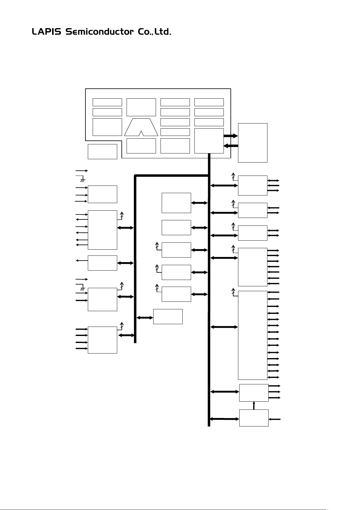
Program
RAM
CPU (nX-U8/100) Large Model
Timing
SP
BUS
TBC
INT 4 INT
6
P20 to P23
INT 4 P52 to P53
Data-bus
TEST0
RESET_N
POWER
V
EPSW1~3
ELR1~3
ECSR1~3
GREG
VSS
OUTCLK*
RXD0*1, RXD1*1
TXD0*1, TXD1*1
INT 2 LSCLK*
P40 to P43
On-Chip
P00 to P03
SCK0*1, SCK1*1
SIN0*1, SIN1*1
SOUT0*1, SOUT1*1
INT
2
WDT
INT
10bit-ADC
AIN0 to AIN11*3
VDD
VSS
OSC0*
1
INT
I2C
INT 1 SDA*1
SCL*1
PWM
INT 3 PWM4*1
PWM5*1
LCD
COM0 to COM3*2
SEG0 to SEG7
LCD
V
*2
, V
*2
, VL3
XT0
XT1
P90 to P91
BLD
PW45EV0*1
P30 to P35*3
INT 1 P10 to P11
OSC1*
TEST1_N
P44 to P47*3
*2
PW45EV1*1
PC0 to PC7*2
PD0 to PD7*2
PF0 to PF7*2
P50 to P51*3
CMP
CMP0P
4
CMP0M
4
CMP1P
4
CMP1M
4
2
INT
PW6EV0*1
PW6EV1*1
PWM6*1
P80 to P85*2
P36
*1 Secondary or tertiary function
1.2 Configuration of Functional Blocks
1.2.1 Block Diagram of ML610Q174
ML610Q174 User’s Manual
Chapter 1 Overview
V
DDL
PSW
Controller
0~15
ALU
LR
EA
DSR/CSR
PC
Memory
Instruction
Decoder
Instruction
Register
ICE
DD
Controller
(Flash)
128Kbyte
SSIO
RESET &
TEST
OSC
4096byte
Interrupt
Controller
UART
8bit Timer
×6
V
REF
*
*
*
*
*2 Select I/O port or LCD driver
*3 Select I/O port or A/D converter input
*4 Select I/O port or Analog comparator input
Figure 1-1 Block Diagram of ML610Q174
GPIO
Driver
BIAS
SEG8 to SEG23
SEG32 to SEG39*2
L1
L2
FEUL610Q174 1-4
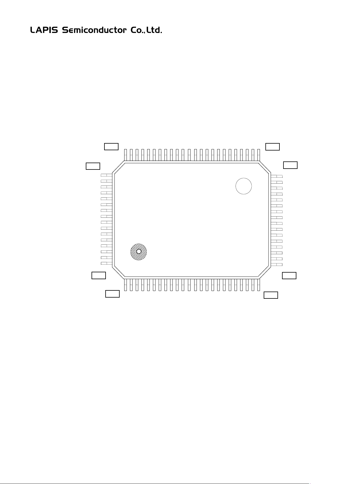
PC3/SEG11
PC1/SEG9
SEG7
SEG6
SEG4
SEG3
SEG2
SEG1
SEG0
PD3/SEG19
PD2/SEG18 PD1/SEG17
64pin
1
2
9
10
11
15
16
17
18
19
20
21
22
23
24
PC7/SEG15
PC6/SEG14
PC5/SEG13
25
26
28
29
30
31
32
33
34
35
36
37
38
39
40
63
61
60
59
57
56
55
54
52
51
50
49
48
47
46
45
44
43
42
41
80
79
78
77
76
75
74
73
72
71
70
69
68
67
66
65
P83/COM3
VL3
P85/VL2
P84/VL1
P36/LSCLK
XT1
XT0
V
DDL
VDD
VSS
P11/OSC1
P10/OSC0
RESET_N
P81/COM1
P82/COM2
P80/COM0
PD7/SEG23
PD6/SEG22
PD5/SEG21
PF3/SEG35/TXD0/PWM4/TXD1
PF4/SEG36/SIN1/PWM4
PF5/SEG37/SCK1/PWM5
TEST0
P00/EXI0/PW45EV0
P01/EXI1/PW6EV0
P02/EXI2/RXD0
P03/EXI3/RXD1
PF0/SEG32/SIN0
PF7/SEG39/TXD1/TXD0
PF6/SEG38/RXD1/SOUT1/PWM6
P21/LED1/OUTCLK/PWM5
P51/AIN9/SCK1
P45/AIN5/SCK0
P35/AIN10/PWM5
SS
P22/LED2/TM9OUT
1.3 Pins
1.3.1 Pin Layout
1.3.1.1 Pin Layout of ML610Q174 QFP Package
ML610Q174 User’s Manual
Chapter 1 Overview
PF1/SEG33/SCK0
PF2/SEG34/ RXD0/SOUT0
TEST1_N
P20/LED0/LSCLK/PWM4
65pin
80pin
1pin
64
V
PD4/SEG20
62
3 4 5 6 7
P91/LED5
P90/LED4
P40/SDA/SIN0
P23/LED3/TMBOUT
PD0/SEG16
58
8
PC4/SEG12
PC2/SEG10
PC0/SEG8
53
12
14
13
SEG5
REF
V
41pin
40pin
27
25pin
24pin
P33/AIN3 P32/AIN2
P41/SCL/SCK0
P34/AIN11/PWM4
P50/AIN8/SIN1
P42/RXD0/SOUT0
P43/TXD0/PWM4/TXD1
P52/RXD1/SOUT1/CMP0P
P47/AIN7/PWM5/CMP1M
P46/AIN6/SOUT0/CMP0M
P44/AIN4/SIN0
P31/AIN1/PW6EV1
P30/AIN0/PW45EV1
P53/TXD1/PWM6/TXD0/CMP1P
FEUL610Q174 1-5
Figure 1-3 Pin Layout of ML610Q174 Package

ML610Q174 User’s Manual
1,27
Power supply for internal logic
(internally generated)
30
XT0
I
Low-speed clock oscillati on pi n
31
XT1
O
Low-speed clock oscillati on pi n
Reference power supply pin of
ADC
P00/EXI0/
PW45EV0
Input port / External interrupt /
PW45EV0 input
P01/EXI1/
PW6EV0
Input port / External interrupt /
PW6EV0 input
P02/EXI2/
RXD0
Input port / External interrupt /
UART0 data input
High-speed clock
oscillation pin
High-speed clock
oscillation pin
Low-speed clock
output
Low-speed clock
output
Input/output port /
ADC input
Input/output port /
ADC input
Input/output port /
ADC input
Input/output port /
ADC input
Input/output port /
ADC input
Input/output port /
ADC input
Low-speed
clock output
Chapter 1 Overview
1.3.2 List of Pins
Table 1-1 lists the pins.
In the I/O col umn, “—” denotes a power supply pin (for primary functions only), “I” an input pin, “O” an output pin,
and “I/O” an input/output pin.
Pin
No.
28
29
34
73
74
32
Pin
name
Vss Negative power supply pin
Positive power supply pin
V
DD
V
DDL
Power supply pin for LCD bias
V
L3
TEST0 I/O Input/output pi n for testing
TEST1_N I/O Input/output pin for testing
RESET_N I Reset input pin
Primary function Secondary function Tertiary function
I/O Description
Pin
name
I/O Description
Pin
name
I/O Description
I
V
24
75
76
77
78
25
26
79
80
2
3
23
22
21
20
10
11
33
REF
P03/EXI3/
RXD1
P10 I Input port OSC0 I
P11 I Input port OSC1 O
P20/LED0 O Output port / LED drive LSCLK O
P21/LED1 O Output port / LED drive OUTCLK O
P22/LED2 O Output port / LED drive TM9OUT O Timer9 output
P23/LED3 O Output port / LED drive TMBOUT O TimerB output
P30/
PW45EV1
/AIN0
P31/
PW6EV1
AIN1
P32/
AIN2
P33/
AIN3
P34/
AIN11
P35/
AIN10
P36 I/O Input/output port LSCLK O
Successive-approximation type
I
I
I
Input port / External interrupt /
I
UART1 data input
PW45EV1 input /
I/O
Successive approximation type
PW6EV1 input /
I/O
Successive approximation type
I/O
Successive approximation type
I/O
Successive approximation type
I/O
Successive approximation type
I/O
Successive approximation type
PWM4 O PWM4 output
PWM5 O PWM5 output
PWM4 O PWM4 output
PWM5 O PWM5 output
FEUL610Q174 1-6
I2C data
input/output
SSIO0 data
input
SSIO0
input/output
UART0
data input
SSIO0 data
output
UART0
data output
PWM4
output
UAR1
data output
Input/output port /
PWM4 external
type ADC input
Input/output port/
type ADC input
Input/output port /
inverting input
Input/output port /
inverting input
Input/output port /
type ADC input
Input/output port /
type ADC input
SSIO1
input/output
Input/output port /
non-inverting input
Input/output port /
non-inverting input
P80/
COM0
Input/output port /
P81/
COM1
Input/output port /
LCD common pin
P82/
COM2
Input/output port /
LCD common pin
P83/
COM3
Input/output port /
LCD common pin
Input/output port /
LCD bias
Input/output port/
41
SEG0
O
LCD segment pin
Pin
No.
6
7
ML610Q174 User’s Manual
Chapter 1 Overview
Primary function Secondary function Tertiary function Fourthly function
Pin
name
P40 I/O Input/output port SDA I/O
P41 I/O Input/output port SCL I/O
I/O Description
Pin
name
I/O Description
2
I
C clock
input/output
Pin
name
SIN0 I
SCK0 I/O
I/O Description
synchronous
clock
Pin
name I/O
Description
8
9
19
18
17
16
15
P42 I/O Input/output port RXD0 I
P43 I/O Input/output port TXD0 O
P44/
T0P4CK/
AIN4
P45/
T1P5CK/
AIN5
P46/
T8AP6CK
/
AIN6/
CMP0M
P47/
T9BCK/
AIN7/
CMP1M
P50/
AIN8
Timer0 /
I/O
clock input/
Successive
approximation
Timer1 /
PWM5 external
I/O
clock input/
Successive
approximation
Timer8,A /
PWM6 external
clock input /
I
Successive
approximation
type ADC input /
Comparator0
Timer9,B external
clock input /
Successive
I
approximation
type ADC input /
Comparator1
Successive
I/O
approximation
SIN0 I
SCK0 I/O
SOUT0 O
PWM5 O
SIN1 I
SOUT0 O
PWM4 O
SSIO0 data
input
SSIO0
synchronous
clock
input/output
SSIO0 data
output
PWM5
output
SSIO1 data
input
TXD1 O
14
13
12
40
39
38
37
36
35
4
5
FEUL610Q174 1-7
P51/
AIN9
P52/
CMP0P
P53/
CMP1P
P84/
V
L1
P85/
V
L2
P90/
LED4
P91/
LED5
Successive
I/O
approximation
I/O
Comparator0
I/O
Comparator1
I/O
LCD common pin
I/O
I/O
I/O
I/O
Power supply pin for
I/O
Power supply pin for
LCD bias
Output port /
O
LED drive
Output port /
O
LED drive
SCK1 I/O
RXD1 I
TXD1 O
UART1
data input
UART1
data input
SOUT1 O
PWM6 O
synchronous
clock
SSIO1 data
output
PWM6
output
TXD0 O
data output
UAR0
ML610Q174 User’s Manual
42
SEG1
O
LCD segment pin
43
SEG2
O
LCD segment pin
44
SEG3
O
LCD segment pin
45
SEG4
O
LCD segment pin
SEG5
O
LCD segment pin
47
SEG6
O
LCD segment pin
48
SEG7
O
LCD segment pin
PC0 /
SEG8
Input/output port /
LCD segment pin
PC1 /
Input/output port /
PC2 /
SEG10
Input/output port /
LCD segment pin
PC3 /
SEG11
Input/output port /
LCD segment pin
PC4 /
SEG12
Input/output port /
LCD segment pin
PC5 /
SEG13
Input/output port /
LCD segment pin
PC6 /
SEG14
Input/output port /
LCD segment pin
PC7 /
SEG15
Input/output port /
LCD segment pin
PD0 /
SEG16
Input/output port /
LCD segment pin
PD1 /
SEG17
Input/output port /
LCD segment pin
PD2 /
SEG18
Input/output port /
LCD segment pin
PD3 /
SEG19
Input/output port /
LCD segment pin
PD4 /
SEG20
Input/output port /
LCD segment pin
PD5 /
SEG21
Input/output port /
LCD segment pin
PD6 /
SEG22
Input/output port /
LCD segment pin
PD7 /
SEG23
Input/output port /
LCD segment pin
PF0 /
SEG32
Input/output port /
LCD segment pin
SSIO0 data
input
SSIO0
input/output
PF2 /
SEG34
Input/output port /
LCD segment pin
UART0
data input
SSIO0 data
output
PF3 /
SEG35
Input/output port /
LCD segment pin
UART0
data output
PWM4
output
UAR1
data output
PF4 /
Input/output port /
SSIO1 data
PWM4
SSIO1
input/output
PF6 /
SEG38
Input/output port /
LCD segment pin
UART1
data input
SSIO1 data
output
PWM6
output
PF7 /
SEG39
Input/output port /
LCD segment pin
UART1
data input
UAR0
data output
Chapter 1 Overview
Pin
No.
46
49
50
51
52
53
54
55
56
57
58
59
60
61
62
63
64
65
Primary function Secondary function Tertiary function Fourthly function
Pin
name
SEG9
I/O Description
I/O
I/O
LCD segment pin
I/O
I/O
I/O
I/O
I/O
I/O
I/O
I/O
I/O
I/O
I/O
I/O
I/O
I/O
I/O
Pin
name
I/O Description
SIN0 I
Pin
name
I/O Description
Pin
name I/O
Description
66
67
68
69
70
71
72
PF1 /
SEG33
SEG36
PF5 /
SEG37
Input/output port /
I/O
LCD segment pin
I/O
I/O
I/O
LCD segment pin
Input/output port /
I/O
LCD segment pin
I/O
I/O
SCK0 I/O
RXD0 I
TXD0 O
SIN1 I
SCK1 I/O
RXD1 I
TXD1 O
SOUT0 O
PWM4 O
SOUT1 O
TXD0 O
synchronous
clock
input
synchronous
clock
TXD1 O
PWM4 O
PWM5 O
PWM6 O
output
PWM5
output
FEUL610Q174 1-8
ML610Q174 User’s Manual
are connected across this pin and VSS as required.
Chapter 1 Overview
1.3.3 Pin Description
Table 1-2 shows the pin description.
In the I/O column, “—” denotes an input pin, “I” an input pin, “O” an output pin, and “I/O” an input/output pin.
Table 1-2 Pin Description
Primary/
Pin name I/O Description
Secondary
Power supply
VSS —
VDD —
V
—
DDL
VL1 —
VL2 —
VL3 —
Negative power supply pin
Positive power supply pin
Positive power supply pin for internal logic (internally generated). Connect
capacitors (C
) (see Measuring Circuit 1) between this pin and VSS .
L
Power supply pins for LCD bias (external input). This function is allocated
to the primary function of the P84 pin.
Power supply pins for LCD bias (external input). This function is allocated
to the primary function of the P85 pin.
Power supply pins for LCD bias (external input)
— —
— —
— —
— —
— —
— —
Test
TEST0
TEST1_N
Input/output pin for testing. This pin has a pull-down resistor built in.
I/O
Input/output pin for testing. This pin has a pull-up resistor built in.
I/O
— Positive
— Negative
System
Reset input pin. When this pin is set to a “L” level, the device is placed in
RESET_N I
system reset mode and the internal circuit is initialized. If after that this pin
is set to a “H” level, program execution starts. This pin has a pull-up
— Negative
resistor built in.
XT0 I
XT1 O — —
OSC0 I
OSC1 O
LSCLK O
OUTCLK O
Crystal connection pin for low-speed clock. A 32.768 kHz crystal oscillator
(see measuring circuit 1) is connected to this pin. Capacitors C
and CGL
DL
Crystal/ceramic connection pin for high-speed clock.
A 8MHz crystal or ceramic is connected to this pin. Capacitors C
C
(see measuring circuit 1) are connected across this pin and VSS.
GH
DH
and
Low-speed clock output. This function is allocated to the secondary
function of the P20/P36 pin.
High-speed clock output. This function is allocated to the secondary
function of the P21 pin.
— —
— —
—
Secondary —
Secondary —
Logic
—
FEUL610Q174 1-9

Provided with a secondary function for
Provided with a LCD segment for each
Pin name I/O Description
General-purpose input port
P00 to P03 I
P10 to P11 I
General-output input port
P20 to P23 O
P90 to P91 O
General-purpose input/output port
P30 to P36
P40 to P47
P50 to P53
P80 to P85
PC0 to PC7
PD0 to PD7
PF0 to PF7
General-purpose input ports. Provided with a secondary function for each
port. Cannot be used as ports if their secondary functions are used.
General-purpose output ports.Provided with a secondary function for each
port. Cannot be used as ports if their secondary functions are used.
General-purpose output ports.Provided with a secondary function for each
port. Cannot be used as ports if their secondary functions are used.
General-purpose input/output ports.
each port. Cannot be used as ports if their secondary functions are used.
I/O
General-purpose input/output ports.
port. Cannot be used as ports if LCD segment are used.
ML610Q174 User’s Manual
Chapter 1 Overview
Primary/
Logic
Secondary
Primary Positive
Primary Positive
Primary Positive
Primary Positive
FEUL610Q174 1-10
ML610Q174 User’s Manual
2
2
Chapter 1 Overview
Pin name I/O Description
UART
TXD0 O
RXD0 I
TXD1 O
RXD1 I
UART0 data output pin. Allocated to the secondary function of the P43 and
PF3 pins and the fourthly function of the P53 and PF7 pins
UART0 data input pin. Allocated to the primary function of the P02 pin and
the secondary function of the P42 and PF2 pins.
UART1 data output pin. Allocated to the secondary function of the P53 and
PF7 pins and the fourthly function of the P43 and PF3 pins.
UART1 data input pin. Allocated to the primary function of the P03 pin and
the secondary function of the P52 and PF6 pins.
I2C bus interface
C data input/output pin. This pin is used as the secondary function of the
I
SDA I/O
SCL I/O
P40 pin. This pin has an NMOS open drain output. When using this pin as
a function of the I
C clock output pin. This pin is used as the secondary function of the P41
I
pin. This pin has an NMOS open drain output. When using this pin as a
function of the I
2
C, externally connect a pull-up resistor.
2
C, externally connect a pull-up resistor.
Synchronous serial (SSIO)
SIN0 I
SCK0 I/O
SOUT0 O
SIN1 I
SCK1 I/O
SOUT1 O
Synchronous serial data input pin. Allocated to the tertiary function of the
P40 and P44 and PF0 pins.
Synchronous serial clock input/output pin. Allocated to the tertiary function
of the P41 and P45 and PF1 pins.
Synchronous serial data output pin. Allocated to the tertiary function of the
P42 and P46 and PF2 pins.
Synchronous serial data input pin. Allocated to the tertiary function of the
P50 and PF4 pins.
Synchronous serial clock input/output pin. Allocated to the tertiary function
of the P51 and PF5 pins.
Synchronous serial data output pin. Allocated to the tertiary function of the
P52 and PF6 pins.
PWM
PWM4 O
PWM5 O
PWM6 O
T0P4CK I
T1P5CK I
T8AP6CK I
PW45EV0
PW45EV1
PW6EV0
PW6EV1
PWM4 output pin. Allocated to the tertiary function of the P34 and P43 and
P20 and PF3 and PF4 pins.
PWM5 output pin. Allocated to the tertiary function of the P35 and P47 and
P21 and PF5 pins.
PWM6 output pin. Allocated to the tertiary function of the P53 and PF6
pins.
External clock input pin for timer 0 and PWM4. Allocated to the primary
function of the P44 pin.
External clock input pin for timer 1 and PWM5. Allocated to the primary
function of the P45 pin.
External clock input pin for timer 8 and timer A and PWM6. Allocated to the
primary function of the P46 pin.
Control start /stop pin for PWM4 and PWM5. Allocated to the primary
I
function of the P00 and P30 pins.
Control start /stop pin for PWM6. Allocated to the primary function of the
I
P01 and P31 pins.
Primary/
Secondary
Secondary
Fourthly
Logic
Positive
Secondary Positive
Secondary
Fourthly
Positive
Secondary Positive
Secondary Positive
Secondary Positive
Tertiary Positive
Tertiary —
Tertiary Positive
Tertiary Positive
Tertiary —
Tertiary Positive
Tertiary Positive
Tertiary Positive
Tertiary Positive
Primary —
Primary —
Primary —
Primary
Primary
—
—
FEUL610Q174 1-11
ML610Q174 User’s Manual
It is possible, for each bit, to specify
whether the interrupt is enabled and select the interrupt edge by software.
P23 pins
LCD segment output pins. Allocated to the secondary function of the
Chapter 1 Overview
Pin name I/O Description
External interrupt
External maskable interrupt input pins.
EXI0–EXI3 I
Allocated to the primary function of the P00–P03 pins.
Timer
T0P4CK I
T1P5CK I
T8AP6CK I
T9BCK I
TM9OUT
TMBOUT
External clock input pin for timer 0 and PWM4. Allocated to the primary
function of the P44 pin.
External clock input pin for timer 1 and PWM5. Allocated to the primary
function of the P45 pin.
External clock input pin for timer 8 and timer A and PWM6. Allocated to the
primary function of the P46 pin.
External clock input pin for timer 9 and timer B. Allocated to the primary
function of the P47 pin.
Timer9 overflow output pin. Allocated to the secondary function of the P22
pin.
TimerB overflow output pin. Allocated to the secondary function of the P23
pin.
LED drive
LED0-LED5 O
Pins for LED driving. Allocated to the primary function of the P20–
and P90–P91 pins.
Successive-approximation type A/D converter
V
I
REF
Reference power supply pin for successive approximation type A/D
converter.
Analog inputs to Ch0–Ch11 of the successive-approximation type A/D
AIN0–AIN11 I
converter. Allocated to the secondary function of the P30 to P35 and P44
to P47 and P50 to P51 pins.
Analog Comparator
CMP0P I
CMP0M I
CMP1P I
CMP1M I
Non-inverting input for comparator0. This pin is used as the primary
function of the P52 pin.
Inverting input for comparator0. This pin is used as the primary function of
the P46 pin.
Non-inverting input for comparator1. This pin is used as the primary
function of the P53 pin.
Inverting input for comparator1. This pin is used as the primary function of
the P47 pin.
LCD driver
COM0 to COM3 O
SEG0 to SEG7 O
SEG8 to SEG23
SEG32 to SEG39
LCD common output pins.
LCD segment output pins.
O
PC0 to PC7 and PD0 to PD7 and PF0 to PF7 pins.
Primary/
Secondary
Primary
Logic
Positive/
Negative
Primary —
Primary —
Primary —
Primary —
Tertiary Positive
Tertiary Positive
Primary
— —
— —
— —
— —
— —
— —
— —
— —
— —
Positive/
Negative
FEUL610Q174 1-12
P20 to P23
open
P50 to P51 (AIN8 to AIN9)
open
1.3.4 Termination of Unused Pins
Table 1-3 shows the recommended termination of unused pins.
Table 1-3 Termination of Unused Pins
Pin Recommended pin termination
RESET_N open
TEST0 open
TEST1_N open
V
Connect to VDD
REF
VL3 open
P00 to P03 Connect V
P10 to P11 Connect V
P30 to P33 (AIN0 to AIN3) open
P34 to P35 (AIN11, AIN10) open
P36 open
P40 to P43 open
P44 to P47 (AIN4 to AIN7) open
DD
DD
ML610Q174 User’s Manual
Chapter 1 Overview
or VSS
or VSS
P52 to P53 open
P80 to P85 open
P90 to P91 open
SEG0 to SEG7 open
PC0 to PC7 (SEG8 to 15) open
PD0 to PD7 (SEG16 to 23) open
PF0 to PF7 (SEG32 to 39) open
Note:
For unused input ports o r unused inp ut/output p orts, i f the corr espondi ng pins are c onfigured a s high-impedance inputs
and left open, the supply current may become excessively large. Therefore, it is recommended to configure those pins as
either inputs with a pull-down resistor/pull-up resistor or outputs.
FEUL610Q174 1-13

Chapter 2
CPU and Memory Space

ML610Q174 User’s Manual
Chapter 2 CPU and Memory Space
2. CPU and Memory Space
2.1 Overview
This LSI incorporates 8-bit CPU nX-U8/100, and a LARGE model is selected for the memory model.
For details of the CPU nX-U8/100, refer to the “nX-U8/100 Core Instruction Manual”.
2.2 Program Memory Space
The program memory space is used to store program codes, table data (ROM window), or vector tables.
The program codes have a length of 16 bits and are specified by a 16-bit program counter (PC).
The ROM window area contains data having a length of 8 bits and can be used as table data.
The vector table, which has 16-bit long data, can be used as reset vectors, hardware interrupt vectors, and software
interrupt vectors.
The program memory space consists of 2 segment and has a total capacity of 128 Kbytes (64 Kwords).
Figure 2-1 shows the configuration of the program memory space.
CSR:PC
0:0FFFFH
0:0FC00H
0:0FBFFH
Segment 0
0:0000H~0FFFFH CSR:PC
Test data area
1:0FFFFH
Segment 1
1:0000H~0FFFFH
Program code
0:0100H
0:00FFH
0:0000H
or
ROM window area
Vector table area,
program code,
or
ROM window area
1:0000H
8bit 8bit
Program code
or
ROM window area
Figure 2-1 Configuration of Program Memory Space
Notes:
• The 1K-byte (512-word) test data area (0:FC00H to 0:FFFFH) of Segment 0 is a test data area. Out of the test data
area, the area 0:FC00H to 0:FDFFH is writable and erasable and the area 0:FE00H to 0:FFFFH is disabled for both
write and erase. The area 0:FC00H to 0:FDFFH is an ISP boot area. When use it as an ISP boot area, write in a
boot program by an on-chip ICE function. Set Code-Option in the area 0:FDE0H, and always write "0FFH" in the
area 0:FDE2H to 0:FDFFH. Operation is not guaranteed if the state where it does not write in or any other value than
“0FFH” is written.
• Set “0FFH” data (BRK instruction) in the unused area of the program memory space for fail-safe reasons.
FEUL610Q174-01 2-1

ML610Q174 User’s Manual
Chapter 2 CPU and Memory Space
2.3 Data Memory Space
The data memory space of this LSI consists of the ROM window area, 4-Kbyte RAM area, SFR area, and the ROM
reference area of Segment 1, the FLASH data area of Segment 2, and the ROM reference area of Segment 8 to Segment
A.
The data memory stores 8-bit data and is specified by 20 bits consisting of higher 4 bits as DSR and lower 16 bits as
addressing specified by instructions.
Figure 2-2 shows the configuration of the data memory space.
DSR:data add Segment 0 Segment 1 Segment 2
0:0FFFFH
0:0F000H
0:0EFFFH
0:0E000H
SFR area
RAM area
4Kbyte
1:0FFFFH 2:0FFFFH
ROM reference
area
Unused area
ROM Window area
0:0000H
8bit 8bit 8bit
1:0000H
2:0800H
2:07FFH
2:0000H
FLASH data
area
Segment 8 Segment 9 Segment A
8:0FFFFH 9:0FFFFH 0A:0FFFFH
8:0FC00H
8:0000H
8bit 8bit 8bit
Test data area
ROM reference
area
9:0000H
ROM reference
area
0A:0800H
0A:07FFH
0A:0000H
Unused area
FLASH data
area
Figure 2-2 Configuration of Data Memory Space
Notes:
• The contents of the 4-Kbyte RAM area are undefined at system reset. Initialize this area by software.
• The contents of the segment 0 of program memory space are read from the ROM reference area of a segment 8.
• The contents of the segment 1 of program memory space are read from the ROM reference area of a segment 9.
• The contents of the segment 2 of program memory space are read from the ROM reference area of a segment A.
• Self rewriting of a flash memory is possible for the data memory area of a segment 2. Please Refer to "Chapter 30
Flash Memory Self Rewriting Function" for Details of Self Rewriting of Flash Memory.
FEUL610Q174-01 2-2

2.4 Instruction Length
One instruction has a length of 16 bits.
2.5 Data Type
The two data types of byte (8 bits) and word (16 bits) are supported.
ML610Q174 User’s Manual
Chapter 2 CPU and Memory Space
FEUL610Q174-01 2-3

ML610Q174 User’s Manual
Chapter 2 CPU and Memory Space
2.6 Description of Registers
2.6.1 List of Registers
Address Name Symbol (Byte) Symbol (Word) R/W Size
0F000H Data segment register DSR ⎯ R/W 8 00H
Initial
value
FEUL610Q174-01 2-4

ML610Q174 User’s Manual
Chapter 2 CPU and Memory Space
2.6.2 Data Segment Register (DSR)
Address: 0F000H
Access: R/W
Access size: 8 bits
Initial value: 00H
7 6 5 4 3 2 1 0
DSR ⎯ ⎯ ⎯ ⎯ DSR3 DSR2 DSR1 DSR0
R/W R R R R R/W R/W R/W R/W
Initial value 0 0 0 0 0 0 0 0
DSR is a special function register (SFR) used to retain a data segment. For details of DSR, refer to the “nX-U8/100
Core Instruction Manual”.
[Description of Bits]
• DSR3-DSR0 (bits 3-0)
DSR3 DSR2 DSR1 DSR0 Description
0 0 0 0 Data segment 0 (initial value)
0 0 0 1 Data segment 1
0 0 1 0 Data segment 2
0 0 1 1
0 1 0 0
0 1 0 1
0 1 1 0
0 1 1 1
1 0 0 0 Data segment 8
1 0 0 1 Data segment 9
1 0 1 0 Data segment A
1 0 1 1
1 1 0 0
1 1 0 1
1 1 1 0
1 1 1 1
Setting prohibited
Setting prohibited
FEUL610Q174-01 2-5

Chapter 3
Reset Function

ML610Q174 User’s Manual
Chapter 3 Reset Function
3 Reset Function
3.1 Overview
This LSI has the four reset functions shown below. If any of the five reset conditions is satisfied, this LSI enters system
reset mode.
• Reset by the RESET_N pin
• Reset by the 2
• Software reset by execution of the BRK instruction
3.1.1 Features
• The RESER_N pin has an internal pull-up resistor
• 125 ms, 500m sec, 2 sec, or 8 sec can be selected as the watchdog timer (WDT) overflow period
• Built-in reset status register (RSTAT) indicating the reset generation causes
• Only the CPU is reset by the BRK instruction (neither the RAM area nor the SFR area are reset).
3.1.2 Configuration
nd
watchdog timer (WDT) overflow
Figure 3-1 shows the configuration of the reset generation circuit.
VDD
RESET_N
WDT Reset
RSTAT :Reset status register
Figure 3-1 Configuration of Reset Generation Circuit
3.1.3 List of Pin
Pin name I/O Description
RESET_N I Reset input pin
RSTAT
RESET
Data bus
FEUL610Q174-01 3-1

ML610Q174 User’s Manual
Chapter 3 Reset Function
3.2 Description of Registers
3.2.1 List of Registers
Address Name Symbol (Byte) Symbol (Word) R/W Size Initial value
0F001H Reset status register RSTAT - R/W 8 ―
3.2.2 Reset Status Register (RSTAT)
Address:0F001H
Access:R/W
Access size:8 bits
Initial value:Undefined
7 6 5 4 3 2 1 0
RSTAT ― ― ― ― ― WDTR ― ―
R/W R R R R R R/W R R
Initial value 0 0 0 0 0 0 0 x
RSTAT is a special function register (SFR) that indicates the causes by which the reset is generated.
At the occurrence of reset, the contents of RSTAT are not initialized, while the bit indicating the cause of the reset is
set to ”1”. When checking the reset cause using this function, perform write operation to RSTAT in advance and
initialize the contents of RSTAT to “00H”.
[Description of Bits]
• WDTR (bit 2)
The WDTR is a flag that indicates that the watchdog timer reset is generated. This bit is set to “1” when the reset by
overflow of the watchdog timer is generated.
WDTR Description
0 Watchdog timer reset not occurred
1 Watchdog timer reset occurred
Note:
No flag is provided that indicates the occurrence of reset by the RESET_N pin.
FEUL610Q174-01 3-2

ML610Q174 User’s Manual
Chapter 3 Reset Function
3.3 Description of Operation
3.3.1 Operation of System Reset Mode
System reset has the highest priority among all the processings and any other processing being executed up to then is
cancelled.
The system reset mode is set by any of the following causes.
• Reset by the RESET_N pin
• Reset by watchdog timer (WDT) overflow
• Software reset by the BRK instruction (only the CPU is reset)
In system reset mode, the following processing is performed.
(1) The power circuit is in itialized, but not initialized by th e reset by the BRK in struction executio n. For the details of
the power circuit, refer to Chapter 29, “Power Circuit”.
(2) All the special function registers (SFRs) whose initial value is not undefined are initialized. However, the
initialization is not performed by software reset due to execution of the BRK instruction. See Appendix A
“Registers” for the initial values of the SFRs.
(3) CPU is initialized.
• All the registers in CPU are initialized.
• The contents of addresses 0000H and 0001H in the program memory are set to the stack pointer (SP).
• The contents of addresses 0002H and 0003H in the program memory are set to the program counter (PC).
However, when the interrupt level (ELEEVL) of the program status word (PSW) at reset by the BRK instruction
is 1 or lower, the contents of addresses 0004H and 0005H of the program memory are set in the program counter
(PC). For the BRK instruction, see “nX-U8/100 Core Instruction Manual”.
Note:
In system reset mode, the contents of data memory and those of any SFR whose initial value is undefined are not
initialized and are undefined. Initialize them by software.
In system reset mode by the BRK instruction, no special function register (SFR) that has a fixed initial value is
initialized either. Therefore initialize such an SFR by software.
FEUL610Q174-01 3-3

Chapter 4
MCU Control Function

ML610Q174 User’s Manual
Chapter 4 MCU Control Function
4. MCU Control Function
4.1 Overview
The operating states of this LSI are classified into the following 4 modes including system reset mode:
(1) System reset mode
(2) Program run mode
(3) HALT mode
(4) STOP mode
For system reset mode, see Chapter 3, “Reset Function”.
This LSI has a block control function which can reduce the supply current more by shut the operation(reset the register
and stop the clock) of the unused function.
4.1.1 Features
• HALT mode, where the CPU stops operating and only the peripheral circuit is operating
• STOP mode, where both low-speed oscillation and high-speed oscillation stop
• Stop code acceptor function, which controls transition to STOP mode
• Block control function, which shut the unused operation(reset the register and stop the clock) of the function.
4.1.2 Configuration
Figure 4-1 shows an operating state transition diagram.
Power on
System reset
mode
Reset
Reset
STP = “1”
Release of reset
Reset or BRK
instruction
External interrupt
HLT = “1”
HALT mode STOP mode
Program
run mode
Interrupt
Figure 4-1 Operating State Transition Diagram
FEUL610Q174-01 4-1

4.2 Description of Registers
4.2.1 List of Registers
ML610Q174 User’s Manual
Chapter 4 MCU Control Function
Address Name Symbol (Byte) Symbol (Word) R/W Size
0F008H Stop code acceptor STPACP ⎯ W 8 ⎯
0F009H Standby control register SBYCON ⎯ W 8 00H
0F028H Block control register 0 BLKCON0 ⎯ R/W 8 00H
0F02AH Block control register 2 BLKCON2 ⎯ R/W 8 00H
0F02CH Block control register 4 BLKCON4 ⎯ R/W 8 00H
0F02EH Block control register 6 BLKCON6 ⎯ R/W 8 00H
0F02FH Block control register 7 BLKCON7 ⎯ R/W 8 00H
Initial
value
FEUL610Q174-01 4-2

ML610Q174 User’s Manual
Chapter 4 MCU Control Function
4.2.2 Stop Code Acceptor (STPACP)
Address: 0F008H
Access: W
Access size: 8 bits
Initial value: − (Undefined)
7 6 5 4 3 2 1 0
STPACP ⎯ ⎯ ⎯ ⎯ ⎯ ⎯ ⎯ ⎯
W W W W W W W W W
Initial value ⎯ ⎯ ⎯ ⎯ ⎯ ⎯ ⎯ ⎯
STPACP is a write-only special function register (SFR) that is used for setting a STOP mode.
When STPACP is read, “00H” is read.
When data is written to STPACP in the order of “5nH”(n : an arbitrary value) and “0AnH”(n: an arbitrary value), the
stop code acceptor is enabled. When the STP bit of the standby control register (SBYCON) is set to “1” in this state,
the mode is changed to the STOP mode. When the STOP mode is set, the STOP code acceptor is disabled.
When another instruction is executed between th e instruction that writes “5nH” to STPACP and the instruction that
writes “0AnH”, the stop code acceptor is enabled after “0AnH” is written. However, if data other than “0AnH” is
written to STPACP after “5nH” is written, the “5nH” write processing becomes invalid so that data must be written
again starting from “5nH”.
During a system reset, the stop code acceptor is disabled.
Note:
The stop code acceptor is not enabled on the condition of that both any interrupt enable flag and the corresponding
interrupt request flag are “1”(An interrupt request occurrence with resetting MIE flag will have the condition).
FEUL610Q174-01 4-3

ML610Q174 User’s Manual
Chapter 4 MCU Control Function
4.2.3 Standby Control Register (SBYCON)
Address: 0F009H
Access: W
Access size: 8 bits
Initial value: 00H
7 6 5 4 3 2 1 0
SBYCON ⎯ ⎯ ⎯ ⎯ ⎯ ⎯ STP HLT
W W W W W W W W W
Initial value 0 0 0 0 0 0 0 0
SBYCON is a special function register (SFR) to control operating mode of MCU.
[Description of Bits]
• STP (bit 1)
The STP bit is used for setting the STOP mode. W hen the STP bit is set to “1” with the sto p code adapter enabled
by using STPACP, the mode is changed to the STOP mode. When the NMI interrupt request or the P00–P03
interrupt request enabled by the interrupt enable register 1 (IE1) is issued, the STP bit is set to “0” and the LSI
returns to the program run mode.
• HLT (bit 0)
The HALT bit is used for setting a HALT mode. W hen the HALT bit is set to “1”, the mode is changed to the
HALT mode. When the NMI interrupt request, WDT interrupt request, or enabled (the interrupt enable flag is “1”)
interrupt request is issued, the HALT bit is set to “0” and the mode is returned to program run mode.
STP HLT Description
0 0 Program run mode (initial value)
0 1 HALT mode
1 0 STOP mode
1 1 Prohibited
Note:
The mode can not be changed to HALT mode or STOP mode on the condition of that both any interrupt enable flag
and the corresponding interrupt request flag are “1”(An interrupt request occurrence with resetting MIE flag will have
the condition).
When a maskable interrupt source (interrupt with enable bit) occurs while the MIE flag of the program status word
(PSW) in the nX-U8/100 core is “0”, the STOP mode and the HALT mode are simply released and interrupt processing
is not performed. Refer to the “nX-U8/100 Core Instruction Manual” for details of PSW.
FEUL610Q174-01 4-4

ML610Q174 User’s Manual
Chapter 4 MCU Control Function
4.2.4 Block Control Register 0 (BLKCON0)
Address: 0F028H
Access: R/W
Access size: 8 bits
Initial value: 00H
7 6 5 4 3 2 1 0
BLKCON0
R/W R R R R R R R/W R/W
Initial value 0 0 0 0 0 0 0 0
⎯ ⎯ ⎯ ⎯ ⎯ ⎯
DTM1 DTM0
BLKCON0 is a special function register (SFR) that controls the operation of the relevant block.
[Description of Bits]
• DTM1 (bit 1)
DTM1 controls the timer 1 operation.
DTM1 Description
0 Enables Timer 1 operation (initial value).
1 Disables Timer 1 operation.
• DTM0 (bit 0)
DTM0 controls the timer 0 operation.
DTM0 Description
0 Enables Timer 0 operation (initial value).
1 Disables Timer 0 operation.
Note:
• If the appropriate bit is set to “1” (operation disabled), the relevant block will be reset (all registers are initialized),
and the clock of the relevant block will stop. When this bit is set to "1", the writing to all the registers of the relevant
block will be invalid, an initial value is read when a register is read. To use the function of the relevant block , reset
(enable operation) the appropriate bit of the block control register to “0”.
• Refer to Chapter 8, “Timers” for details of the timer operation.
FEUL610Q174-01 4-5

ML610Q174 User’s Manual
Chapter 4 MCU Control Function
4.2.5 Block Control Register 2 (BLKCON2)
Address: 0F02AH
Access: R/W
Access size: 8 bits
Initial value: 00H
7 6 5 4 3 2 1 0
BLKCON2 DI2C0 ⎯ ⎯ ⎯ DUA1 DUA0 DSIO1 DSIO0
R/W R/W R R R R/W R/W R/W R/W
Initial value 0 0 0 0 0 0 0 0
BLKCON2 is a special function register (SFR) that controls the operation of the relevant block.
[Description of Bits]
• DI2C0 (bit 7)
DI2C0 controls the operation of I
2
C bus interface.
DI2C0 Description
0 Enables the operation of I2C bus interface (initial value).
1 Disables the operation of I2C bus interface.
• DUA1 (bit 3)
DUA1 controls the operation of UART1.
DUA1 Description
0 Enables the operation of UART1(initial value).
1 Disables the operation of UART1.
• DUA0 (bit 2)
DUA0 controls the operation of UART0.
DUA0 Description
0 Enables the operation of UART0(initial value).
1 Disables the operation of UART0.
• DSIO1 (bit 1)
DSIO1 controls the operation of the synchronous serial port 0.
DSIO1 Description
0 Enables the operation of SSIO1 (initial value).
1 Disables the operation of SSIO1.
• DSIO0 (bit 0)
DSIO0 controls the operation of the synchronous serial port 0.
DSIO0 Description
0 Enables the operation of SSIO0 (initial value).
1 Disables the operation of SSIO0.
FEUL610Q174-01 4-6

ML610Q174 User’s Manual
Chapter 4 MCU Control Function
Note:
• If the appropriate bit is set to “1” (operation disabled), the relevant block will be reset (all registers are initialized),
and the clock of the relevant block will stop. When this bit is set to "1", the writing to all the registers of the relevant
block will be invalid, an initial value is read when a register is read. To use the function of the relevant block , reset
(enable operation) the appropriate bit of the block control register to “0”.
• Refer to Chapter 13, “I
2
C bus interface” for details of the I2C bus interface operation.
• Refer to Chapter 12, “UART” for details of the UART operation.
• Refer to Chapter 11, “Synchronous Serial Port” for details of the SSIO operation.
FEUL610Q174-01 4-7

ML610Q174 User’s Manual
Chapter 4 MCU Control Function
4.2.6 Block Control Register 4 (BLKCON4)
Address: 0F02CH
Access: R/W
Access size: 8 bits
Initial value: 00H
7 6 5 4 3 2 1 0
BLKCON4 ⎯ DLCD DBLD ⎯ ⎯ ⎯ ⎯ DSAD
R/W R R/W R/W R R R R R/W
Initial value 0 0 0 0 0 0 0 0
BLKCON4 is a special function register (SFR) that controls the operation of the relevant block.
[Description of Bits]
• DLCD (bit 6)
DLCD controls the operation of the LCD driver.
DLCD Description
0 Enable the operation of the LCD driver (initial value).
1 Disable the operation of the LCD driver.
• DBLD (bit 5)
The DBLD bit is used to control BLD (Battery Level Detector) operation. Wh en the DBLD bit is set to “1”, the
circuits related to BLD are reset and turned off.
DBLD Description
0 Enable the operation of the BLD (initial value).
1 Disable the operation of the BLD.
• DSAD (bit 0)
The DSAD bit is used to control SA type A/D converter operation. When the DSAD bit is set to “1”, the circuits
related to SA type A/D converter are reset and turned off.
DSAD Description
0 Enable operating SA type A/D converter (initial value)
1 Disable operating SA type A/D converter
Note:
• If the appropriate bit is set to “1” (operation disabled), the relevant block will be reset (all registers are initialized),
and the clock of the relevant block will stop. When this bit is set to "1", the writing to all the registers of the relevant
block will be invalid, an initial value is read when a register is read. To use the function of the relevant block , reset
(enable operation) the appropriate bit of the block control register to “0”.
• Refer to Chapter 25, “LCD driver” for details of the LCD driver operation.
• Refer to Chapter 27, “Battery Level Detector” for details of the Battery Level Detector operation.
• Refer to Chapter 26, “Successive Approximation Type A/D Converter” for details of the successive approximation
type A/D converter operation.
• When P84/VL1, P85/VL2 are used as input/output port, it is required to set BIASMOD register as 02h. When DLCD
bit of BLKCON4 register is “1”, it cannot be written in a BIASMOD register. Therefore, when P84/VL1, P85/VL2 are
used not as LCD driver but as input/output port, set a DLCD bit as “0”.
FEUL610Q174-01 4-8

ML610Q174 User’s Manual
Chapter 4 MCU Control Function
4.2.7 Block Control Register 6 (BLKCON6)
Address: 0F02EH
Access: R/W
Access size: 8 bits
Initial value: 00H
7 6 5 4 3 2 1 0
BLKCON6 ⎯ ⎯ ⎯ ⎯ DTMB DTMA DTM9 DTM8
R/W R R R R R/W R/W R/W R/W
Initial value 0 0 0 0 0 0 0 0
BLKCON6 is a special function register (SFR) that controls the operation of the relevant block.
[Description of Bits]
• DTMB (bit 3)
DTMB controls the operation of the TimerB.
DTMB Description
0 Enable the operation of the TimerB (initial value).
1 Disable the operation of the TimerB.
• DTMA (bit 2)
DTMA controls the operation of the TimerA.
DTMA Description
0 Enable the operation of the TimerA (initial value).
1 Disable the operation of the TimerA.
• DTM9 (bit 1)
DTM9 controls the operation of the Timer9.
DTM9 Description
0 Enable the operation of the Timer9 (initial value).
1 Disable the operation of the Timer9.
• DTM8 (bit 0)
DTMB controls the operation of the Timer 8.
DTM8 Description
0 Enable the operation of the Timer8 (initial value).
1 Disable the operation of the Timer8.
Note:
• If the appropriate bit is set to “1” (operation disabled), the relevant block will be reset (all registers are initialized),
and the clock of the relevant block will stop. When this bit is set to "1", the writing to all the registers of the relevant
block will be invalid, an initial value is read when a register is read. To use the function of the relevant block , reset
(enable operation) the appropriate bit of the block control register to “0”.
• Refer to Chapter 8, “Timer” for details of the Timer operation.
FEUL610Q174-01 4-9

ML610Q174 User’s Manual
Chapter 4 MCU Control Function
4.2.8 Block Control Register 7 (BLKCON7)
Address: 0F02FH
Access: R/W
Access size: 8 bits
Initial value: 00H
7 6 5 4 3 2 1 0
BLKCON7 ⎯ ⎯ ⎯ ⎯ ⎯ DPW6 DPW5 DPW4
R/W R R R R R R/W R/W R/W
Initial value 0 0 0 0 0 0 0 0
BLKCON7 is a special function register (SFR) that controls the operation of the relevant block.
[Description of Bits]
• DPW6 (bit 2)
DPW6 controls the operation of the PWM6.
DPW6 Description
0 Enable the operation of the PWM6 (initial value).
1 Disable the operation of the PWM6.
• DPW5 (bit 1)
DPW5 controls the operation of the PWM5.
DPW5 Description
0 Enable the operation of the PWM5 (initial value).
1 Disable the operation of the PWM5.
• DPW4 (bit 0)
DPW4 controls the operation of the PWM4.
DPW4 Description
0 Enable the operation of the PWM4 (initial value).
1 Disable the operation of the PWM4.
Note:
• If the appropriate bit is set to “1” (operation disabled), the relevant block will be reset (all registers are initialized),
and the clock of the relevant block will stop. When this bit is set to "1", the writing to all the registers of the relevant
block will be invalid, an initial value is read when a register is read. To use the function of the relevant block , reset
(enable operation) the appropriate bit of the block control register to “0”.
• Refer to Chapter 10, “PWM” for details of the PWM operation.
FEUL610Q174-01 4-10

ML610Q174 User’s Manual
Chapter 4 MCU Control Function
4.3 Description of Operation
4.3.1 Program Run Mode
The program run mode is the state where the CPU executes instructions sequentially.
At power-on reset, RESET_N pin reset, WDT overflow reset, the CPU executes instructions from the addresses that are
set in addresses 0002H and 0003H of program memory (ROM) after the system reset mode is released.
At reset by the BRK instruction, the CPU executes instructions from the addresses that are set in the addresses 0004H
and 0005H of the program memory after the system reset mode is released. However, when the value of the interrupt
level bit (ELEVEL) of the program status word (PSW) is 02H or higher at execution of the BRK instruction (after the
occurrence of the WDT interrupt), the CPU executes instructions from the addresses that are set in the addresses 0002H
and 0003H.
For details of the BRK instruction and PSW, see the “nX-U8/100 Core Instruction Manual” and for the reset function,
see Chapter 3, “Reset Function”.
4.3.2 HALT Mode
The HALT mode is the state where the CPU interrupts execution of instructions and only the peripheral circuits are
running.
When the HLT bit of the standby control register (SBYCON) is set to “1”, the HALT mode is set.
When a WDT interrupt request, or an interrupt request enabled by an interrupt enable register (IE0–IE7) is issued, the
HLT bit is set to “0” on the falling edge of the next system clock (SYSCLK) and the HALT mode is returned to the
program run mode released.
Figure 4-2 shows the operation waveforms in HALT mode.
System clock
SYSCLK
CPUCLK
SBYCON.HLT
Interrupt request
Program operating mode HALTmode
Program operating mode
Figure 4-2 Operation Waveforms in HALT Mode
Note:
Since up to two instructions are executed during the period between HALT mode release and a transition to interrupt
processing, place two NOP instructions next to the instruction that sets the HLT bit to “1”.
FEUL610Q174-01 4-11

ML610Q174 User’s Manual
Chapter 4 MCU Control Function
4.3.3 STOP Mode
The STOP mode is the state where low-speed oscillation and high-speed oscillation stop an d the CPU and peripheral
circuits stop the operation.
When the stop code acceptor is enabled by writing “5nH”(n: an arbitrary value) and “0AnH”(n: an arbitrary value) to
the stop code acceptor (STPACP) sequentially and the STP bit of the standby control register (SBYCON) is set to “1”,
the STOP mode is entered. When the STOP mode is set, the stop code acceptor is disabled.
When an interrupt-enabled (the interrupt enable flag is “1”) P0 0 to P03 interrupt request is issu ed, the STP bit is set to
“0”, the STOP mode is released, and the mode is returned to the program run mode.
4.3.3.1 STOP Mode When CPU Operates with Low-Speed Clock
When the stop code acceptor is in the enabled state and the STP bit of SBYCON is set to “1”, the STOP mode is
entered, stopping low-speed oscillation and high-speed oscillation.
When the interrupt-enabled (the interrupt enable flag is “1”) P00 to P03 interru pt request is issued, the STP b it is set to
“0” and low-speed oscillation restarts. If the high-speed clock was oscillating before the STOP mode is entered, the
high-speed oscillation restarts. When the high-speed clock was not oscillating before the STOP mode is entered,
high-speed oscillation does not start.
When an interrupt request occurs, the STOP mode is released after counting a built-in RC oscillation clock 128 times.,
the mode is returned to the program mode, and the low-speed clock(LSCLK) restarts supply to the peripheral circuits.
If the high-speed clock already started oscillation at this time, the high-speed clo cks (OSCLK and HSCLK) also restart
supply to the peripheral circuits. After waiting for low-speed crystal oscillation start time(T
) and low-speed crystal
XTL
oscillation stable time(8192-pulse count), the low-speed clock changes from a built-in RC oscillation clock to the
low-speed crystal oscillation clock. Simultaneously, low-speed oscillation clock change interruption (LOSCINT) is
generated.
Refer to appendix C, “Electrical Characteristics” for T
XTL
.
Figure 4-3 shows the operation waveforms in STOP mode when CPU operates with the low-speed clock.
Low-speed crystal
oscillation
waveform
Hiz
Oscillation waveform
Low-speed clock
T
XTL
pulse count
Built-in RC
oscillation waveform
Built-in RC oscillation
128 pulse count
LSCLK
SYSCLK
High-speed
oscillation
waveform
HSCLK
SBYCON.STP bit
Interrupt request
Program operating mode
Oscillation waveform
HSCLK waveform HSCLK waveform
STOP mode
Oscillation waveform
Program operating mode
Low-speed oscillation clock change
interrupt request
Figure 4-3 Operation Waveforms in STOP Mode When CPU Operates with Low-Speed Clock
4.3.3.2 STOP Mode When CPU Operates with High-Speed Clock
FEUL610Q174-01 4-12

ML610Q174 User’s Manual
equest
Chapter 4 MCU Control Function
When the CPU is operating with a high-speed clock and the STP bit of SBYCON is set to “1” with the stop code
acceptor enabled, the STOP mode is entered and high-speed oscillation and low-speed oscillation stop.
When the interrupt-enabled (the interrupt enable flag is “1”) P00 to P03 interru pt request is issued, the STP b it is set to
“0” and the low-speed and high-speed oscillation restart.
When an interrupt request is issued, the STOP mode is released after the elapse of the high-speed oscillation start time
) and the high-speed clock (OSCLK) oscillation stabilization time (4096-pulse count), the mode is returned to the
(T
XTH
program run mode, and the high-speed clocks (OSCLK and HSCLK) restart supply to the peripheral circuits.
The low-speed clock (LSCLK) restarts supply to the peripheral circuits after counting a built-in RC oscillation clock
128 times. After the elapse of the low-speed oscillation start time (T
) and the oscillation stabilization time
XTL
(8192-pulse count), the clock is returned to the built-in RC oscillation clock to a low-speed crystal oscillation clock.
Simultaneously, low-speed oscillation clock change interruption (LOSCINT) is generated.
Figure 4-4 shows the operation waveforms in STOP mode when CPU operates with the high-speed clock.
High-speed oscillation waveform
High-speed oscillation
waveform
OSCLK, HSCLK
T
OSCLK,HSCLK waveform
High-speed oscillation waveform
XTH
OSCLK, HSCLK waveform
High-speed oscillation 4096 count
SYSCLK
Low-speed crystal
oscillation
Built-in RC
oscillation
LSCLK
SBYCON.STP bit
Interrupt
r
Program operating mode
HSCLK waveform
Hiz
STOP mode
T
XTL
Built-in RC oscillation
128 count
8192 count
Program operating mode
HSCLK waveform
Low-speed crystal
oscillation waveform
Figure 4-4 Operation Waveforms in STOP Mode When CPU Operates with High-Speed Clock
Note:
The STOP mode is entered after the instruction that sets the STP bit to “1” and up to two instructions are executed
during the period between STOP mode release and a transition to interrupt processing. Therefore, place two NOP
instructions next to the instruction that set the STP bit to “1 ”.
FEUL610Q174-01 4-13

ML610Q174 User’s Manual
Chapter 4 MCU Control Function
4.3.3.3 Note on Return Operation from STOP/HALT Mode
The operation of returning from the STOP mode and HALT mode varies according to the interrupt level (ELEVEL) of
the program status word (PSW), master interrupt enable flag (MIE), the contents of the interrupt enable register (IE0 to
IE3), and whether the interrupt is a non-maskable interrupt or a maskable interrupt.
For details of PSW and the IE and IRQ registers, see “nX-U8/100 Core Instruction Manual” and Chapter 5, “Interrupt”,
respectively.
Table 4-1 and Table 4-2 show the return operations from STOP/HALT mode.
Table 4-1 Return Operation from STOP/HALT Mode (Non-Maskable Interrupt)
ELEVEL MIE IEn.m IRQn.m Return operation from STOP/HALT mode
½ ½ ⎯ 0 Not returned from STOP/HALT mode.
After the mode is returned from STOP/HALT mode, the program
3 ½ ⎯ 1
operation restarts from the instruction following the instruction that
sets the STP/HLT bit to “1”. The program operation does not go to
the interrupt routine.
After the mode is returned from the STOP/HALT mode, program
0, 1, 2 ½ ⎯ 1
operation restarts from the instruction following the instruction that
sets the STP/HLT bit to “1”, then goes to the interrupt routine.
Table 4-2 Return Operation from STOP/HALT Mode (Maskable Interrupt)
ELEVEL MIE IEn.m IRQn.m Return operation from STOP/HALT mode
½ ½ ½ 0
½ ½ 0 1
½ 0 1 1
2, 3 1 1 1
0,1 1 1 1
Not returned from STOP/HALT mode.
After the mode is returned from STOP/HALT mode, the program
operation restarts from the instruction following the instruction that
sets the STP/HLT bit to “1”. The program operation does not go to
the interrupt routine.
After the mode is returned from the STOP/HALT mode, program
operation restarts from the instruction following the instruction that
sets the STP/HLT bit to “1”, then goes to the interrupt routine.
Notes:
• If the ELEVEL bit is 0H, it indicates that the CPU is performing neither nonmaskable interrupt processing nor
maskable interrupt processing nor software interrupt processing.
• If the ELEVEL bit is 1H, it indicates that the CPU is performing maskable interrupt processing or software interrupt
processing. (ELEVEL is set during interrupt transition cycle.)
• If the ELEVEL bit is 2H, it indicates that the CPU is performing non-maskable interrupt processing. (ELEVEL is set
during interrupt transition cycle.)
• If the ELEVEL bit is 3H, it indicates that the CPU is performing interrupt processing specific to the emulator. This
setting is not allowed in normal applications.
FEUL610Q174-01 4-14

ML610Q174 User’s Manual
Chapter 4 MCU Control Function
4.3.4 Block control function
To use this block control function, supply current can be reduced more, by stopping completely operation of the unused
function.
The initial value of each bit of each block control register is "0", and operation of each block is enabled. If the
appropriate bit is set to “1” (operation disabled), th e relevant block will be reset (all registers are initialized), and the
clock of the relevant block will stop. When this bit is set to "1", th e writing to all th e registers of th e relevant blo ck will
be invalid, an initial value is read when a register is read. To use the function of the relevant block, reset (enable
operation) the appropriate bit of the block control register to “0”.
BLKCON0,6 register controls (enables or disables) the operation of Timer .
BLKCON2 register controls (enables or disables) the operation of I
2
C UART and SSIO.
BLKCON4 register controls (enables or disables) the operation of the LCD driver, Battery level detecter
successive-approximation type A/D converter.
BLKCON7 register controls (enables or disables) the operation of PWM.
Notes:
• If the appropriate bit of the block register is set to “1”, all relev ant registers are initialized.
• Refer to the relevant chapter for details of operation or notes of each block.
FEUL610Q174-01 4-15

Chapter 5
Interrupts (INTs)

ML610Q174 User’s Manual
Chapter 5 Interrupts (INTs)
5. Interrupts (INTs)
5.1 Overview
This LSI has 27 interrupt sources (External interrupts: 4 sources, Internal interrupts: 23 sources) and a software
interrupt (SWI).
For details of each interrupt, see the following chapters:
Chapter 6, “Clock Generation Circuit”
Chapter 7, “Time Base Counter”
Chapter 8, “Timer”
Chapter 9, “Watchdog Timer”
Chapter 10, “PWM”
Chapter 11, “Synchronous Serial Port”
Chapter 12, “UART”
Chapter 13, “I
Chapter 14, “Port0”
Chapter 26, “Successive Approximation Type A/D Converter”
Chapter 28, “Analog Comparator”
5.1.1 Features
2
C bus interface”
• 1 non-maskable interrupt sources (Internal source: 1)
• 26 maskable interrupt sources (Internal sources: 22, External sources: 4)
• Software interrupt (SWI): 64 sources max.
• External interrupts allow edge selection and sampling selection.
FEUL610Q174-01 5-1

ML610Q174 User’s Manual
Chapter 5 Interrupts (INTs)
5.2 Description of Registers
5.2.1 List of Registers
Address Name Symbol (Byte) Symbol (Word) R/W Size Initial value
0F010H Interrupt enable register 0 IE0 ⎯ R/W 8 00H
0F011H Interrupt enable register 1 IE1 ⎯ R/W 8 00H
0F012H Interrupt enable register 2 IE2 ⎯ R/W 8 00H
0F013H Interrupt enable register 3 IE3 ⎯ R/W 8 00H
0F014H Interrupt enable register 4 IE4 ⎯ R/W 8 00H
0F015H Interrupt enable register 5 IE5 ⎯ R/W 8 00H
0F016H Interrupt enable register 6 IE6 ⎯ R/W 8 00H
0F017H Interrupt enable register 7 IE7 ⎯ R/W 8 00H
0F018H Interrupt request register 0 IRQ0 ⎯ R/W 8 00H
0F019H Interrupt request register 1 IRQ1 ⎯ R/W 8 00H
0F01AH Interrupt request register 2 IRQ2 ⎯ R/W 8 00H
0F01BH Interrupt request register 3 IRQ3 ⎯ R/W 8 00H
0F01CH Interrupt request register 4 IRQ4 ⎯ R/W 8 00H
0F01DH Interrupt request register 5 IRQ5 ⎯ R/W 8 00H
0F01EH Interrupt request register 6 IRQ6 ⎯ R/W 8 00H
0F01FH Interrupt request register 7 IRQ7 ⎯ R/W 8 00H
FEUL610Q174-01 5-2

ML610Q174 User’s Manual
Chapter 5 Interrupts (INTs)
5.2.2 Interrupt Enable Register 0 (IE0)
Address: 0F010H
Access: R/W
Access size: 8 bits
Initial value: 00H
7 6 5 4 3 2 1 0
IE0 ⎯ ELOSC ⎯ ⎯ ⎯ ⎯ ⎯ ⎯
R/W R R/W R R R R R R
Initial value 0 0 0 0 0 0 0 0
IE0 is a special function register (SFR) to control enable/disable for each interrupt request.
When an interrupt is accepted, the master interrupt enable flag (MIE) is set to “0”, but the corresponding flag of IE1 is
not reset.
[Description of Bits]
• ELOSC (bit 6)
ELOSC is the enable flag for the Low-speed clock change interrupt (LOSCINT).
ELOSC Description
0 Disabled (initial value)
1 Enabled
FEUL610Q174-01 5-3

ML610Q174 User’s Manual
Chapter 5 Interrupts (INTs)
5.2.3 Interrupt Enable Register 1 (IE1)
Address: 0F011H
Access: R/W
Access size: 8 bits
Initial value: 00H
7 6 5 4 3 2 1 0
IE1 ⎯ ⎯ ⎯ ⎯ EP03 EP02 EP01 EP00
R/W R R R R R/W R/W R/W R/W
Initial value 0 0 0 0 0 0 0 0
IE1 is a special function register (SFR) to control enable/disable for each interrupt request.
When an interrupt is accepted, the master interrupt enable flag (MIE) is set to “0”, but the corresponding flag of IE1 is
not reset.
[Description of Bits]
• EP00 (bit 0)
EP00 is the enable flag for the input port P00 pin inte rrupt (P00INT).
EP00 Description
0 Disabled (initial value)
1 Enabled
• EP01 (bit 1)
EP01 is the enable flag for the input port P01 pin inte rrupt (P01INT).
EP01 Description
0 Disabled (initial value)
1 Enabled
• EP02 (bit 2)
EP02 is the enable flag for the input port P02 pin inte rrupt (P02INT).
EP02 Description
0 Disabled (initial value)
1 Enabled
• EP03 (bit 3)
EP03 is the enable flag for the input port P03 pin inte rrupt (P03INT).
EP03 Description
0 Disabled (initial value)
1 Enabled
FEUL610Q174-01 5-4

ML610Q174 User’s Manual
Chapter 5 Interrupts (INTs)
5.2.4 Interrupt Enable Register 2 (IE2)
Address: 0F012H
Access: R/W
Access size: 8 bits
Initial value: 00H
7 6 5 4 3 2 1 0
IE2 EI2C0 ⎯ ⎯ ⎯ ⎯ ESAD ESIO1 ESIO0
R/W R/W R R R R R/W R/W R/W
Initial value 0 0 0 0 0 0 0 0
IE2 is a special function register (SFR) to control enable/disable for each interrupt request.
When an interrupt is accepted, the master interrupt enable flag (MIE) is set to “0”, but the corresponding flag of IE2 is
not reset.
[Description of Bits]
• ESIO0 (bit 0)
ESIO0 is the enable flag for the synchronous serial port 0 interrupt (SIO0INT).
ESIO0 Description
0 Disabled (initial value)
1 Enabled
• ESIO1 (bit 1)
ESIO1 is the enable flag for the synchronous serial port 1 interrupt (SIO1INT).
ESIO1 Description
0 Disabled (initial value)
1 Enabled
• ESAD (bit 2)
ESAD is the enable flag for the successive approximation type A/D converter interrupt (SADINT).
ESAD Description
0 Disabled (initial value)
1 Enabled
• EI2C0 (bit 7)
EI2C0 is the enable flag for the successive approximation type A/D converter interrupt (SADINT).
EI2C0 Description
0 Disabled (initial value)
1 Enabled
FEUL610Q174-01 5-5
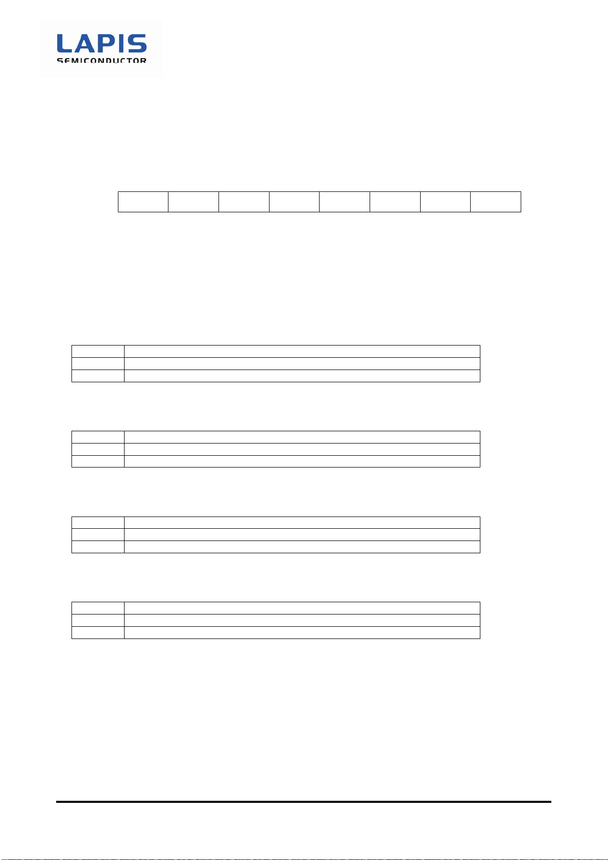
ML610Q174 User’s Manual
(
(
(
(
Chapter 5 Interrupts (INTs)
5.2.5 Interrupt Enable Register 3 (IE3)
Address: 0F013H
Access: R/W
Access size: 8 bits
Initial value: 00H
7 6 5 4 3 2 1 0
IE3 ⎯ ⎯ ⎯ ⎯ ETM9 ETM8 ETM1 ETM0
R/W R R R R R/W R/W R/W R/W
Initial value 0 0 0 0 0 0 0 0
IE3 is a special function register (SFR) to control enable/disable for each interrupt request.
When an interrupt is accepted, the master interrupt enable flag (MIE) is set to “0”, but the corresponding flag of IE3 is
not reset.
[Description of Bits]
• ETM0 (bit 0)
ETM0 is the enable flag for the timer 0 interrupt (TM0INT).
ETM0 Description
0 Disabled
1 Enabled
initial value)
• ETM1 (bit 1)
ETM1 is the enable flag for the timer 1 interrupt (TM1INT).
ETM1 Description
0 Disabled
1 Enabled
initial value)
• ETM8 (bit 2)
ETM8 is the enable flag for the timer 8 interrupt (TM8INT).
ETM4 Description
0 Disabled
1 Enabled
initial value)
• ETM9 (bit 3)
ETM9 is the enable flag for the timer 9 interrupt (TM9INT).
ETM5 Description
0 Disabled
1 Enabled
initial value)
FEUL610Q174-01 5-6

ML610Q174 User’s Manual
(
(
(
(
Chapter 5 Interrupts (INTs)
5.2.6 Interrupt Enable Register 4 (IE4)
Address: 0F014H
Access: R/W
Access size: 8 bits
Initial value: 00H
7 6 5 4 3 2 1 0
IE4 ECMP1 ECMP0 ⎯ ⎯ ⎯ ⎯ EUA1 EUA0
R/W R/W R/W R R R R R/W R/W
Initial value 0 0 0 0 0 0 0 0
IE4 is a special function register (SFR) to control enable/disable for each interrupt request.
When an interrupt is accepted, the master interrupt enable flag (MIE) is set to “0”, but the corresponding flag of IE4 is
not reset.
[Description of Bits]
• EUA0 (bit 0)
EUA0 is the enable flag for the UART0 interrupt (UA0INT).
EUA0 Description
0 Disabled
1 Enabled
initial value)
• EUA1 (bit 1)
EUA1 is the enable flag for the UART1 interrupt (UA1INT).
EUA1 Description
0 Disabled
1 Enabled
initial value)
• ECMP0 (bit 6)
ECMP0 is the enable flag for the CMP0 interrupt (CMP0INT).
ECMP0 Description
0 Disabled
1 Enabled
initial value)
• ECMP1 (bit 7)
ECMP1 is the enable flag for the CMP1 interrupt (CMP1INT).
ECMP1 Description
0 Disabled
1 Enabled
initial value)
FEUL610Q174-01 5-7

ML610Q174 User’s Manual
(
(
Chapter 5 Interrupts (INTs)
5.2.7 Interrupt Enable Register 5 (IE5)
Address: 0F015H
Access: R/W
Access size: 8 bits
Initial value: 00H
7 6 5 4 3 2 1 0
IE5 ETMB ETMA ⎯ ⎯ ⎯ ⎯ ⎯ ⎯
R/W R/W R/W R R R R R R
Initial value 0 0 0 0 0 0 0 0
IE5 is a special function register (SFR) to control enable/disable for each interrupt request.
When an interrupt is accepted, the master interrupt enable flag (MIE) is set to “0”, but the corresponding flag of IE5 is
not reset.
[Description of Bits]
• ETMA (bit 6)
ETMA is the enable flag for the timer A interrupt (TMAINT).
ETMA Description
0 Disabled
1 Enabled
initial value)
• ETMB (bit 7)
ETMB is the enable flag for the timer B interrupt (TMBINT).
ETMB Description
0 Disabled
1 Enabled
initial value)
FEUL610Q174-01 5-8

ML610Q174 User’s Manual
(
(
(
(
(
Chapter 5 Interrupts (INTs)
5.2.8 Interrupt Enable Register 6 (IE6)
Address: 0F016H
Access: R/W
Access size: 8 bits
Initial value: 00H
7 6 5 4 3 2 1 0
IE6 EL32H ⎯ EL128H ⎯ ⎯ EPW6 EPW5 EPW4
R/W R/W R R/W R R R/W R/W R/W
Initial value 0 0 0 0 0 0 0 0
IE6 is a special function register (SFR) to control enable/disable for each interrupt request.
When an interrupt is accepted, the master interrupt enable flag (MIE) is set to “0”, but the corresponding flag of IE6 is
not reset.
[Description of Bits]
• EPW4 (bit 0)
EPW4 is the enable flag for the PWM4 interrupt (PW4INT).
EPW4 Description
0 Disabled
1 Enabled
initial value)
• EPW5 (bit 1)
EPW5 is the enable flag for the PWM5 interrupt (PW5INT).
EPW5 Description
0 Disabled
1 Enabled
initial value)
• EPW6 (bit 2)
EPW6 is the enable flag for the PWM6 interrupt (PW6INT).
EPW6 Description
0 Disabled
1 Enabled
initial value)
• EL128H (bit 5)
EL128H is the enable flag for the time base counter 128 Hz interrupt (TL128HINT).
EL16H Description
0 Disabled
1 Enabled
initial value)
• EL32H (bit 7)
EL32H is the enable flag for the time base counter 32Hz interrupt (TL32HINT).
EL32H Description
0 Disabled
1 Enabled
initial value)
FEUL610Q174-01 5-9

ML610Q174 User’s Manual
Chapter 5 Interrupts (INTs)
5.2.9 Interrupt Enable Register 7 (IE7)
Address: 0F017H
Access: R/W
Access size: 8 bits
Initial value: 00H
7 6 5 4 3 2 1 0
IE7 ⎯ ⎯ ⎯ ⎯ E2H ⎯ ⎯ E16H
R/W R R R R R/W R R R/W
Initial value 0 0 0 0 0 0 0 0
IE7 is a special function register (SFR) to control enable/disable for each interrupt request.
When an interrupt is accepted, the master interrupt enable flag (MIE) is set to “0”, but the corresponding flag of IE7 is
not reset.
[Description of Bits]
• E16H (bit 0)
E16H is the enable flag for the time base counter 16 Hz interrupt (T16HINT).
E16H Description
0 Disabled (initial value)
1 Enabled
• E2H (bit 3)
E2H is the enable flag for the time base counter 2 Hz interrupt (T2HINT).
E2H Description
0 Disabled (initial value)
1 Enabled
FEUL610Q174-01 5-10

ML610Q174 User’s Manual
Chapter 5 Interrupts (INTs)
5.2.10 Interrupt Request Register 0 (IRQ0)
Address: 0F018H
Access: R/W
Access size: 8 bits
Initial value: 00H
7 6 5 4 3 2 1 0
IRQ0 ⎯ QLOSC ⎯ ⎯ ⎯ ⎯ ⎯ QWDT
R/W R R/W R R R R R R/W
Initial value 0 0 0 0 0 0 0 0
IRQ0 is a special function register (SFR) to request an interrupt for each interrupt source.
The watchdog timer interrupt (WDTINT) is non-maskable interrupts that do not depend on MIE. In this case, an
interrupt is requested to the CPU regardless of the value of the Mask Interrupt Enable flag (MIE).
Each IRQ0 request flag is set to “1” regardless of the MIE value when an interrupt is generated. By setting the IRQ0
request flag to “1” by software, an interrupt can be generated.
The corresponding flag of IRQ0 is set to “0” by hardware when the interrupt request is accepted by the CPU.
[Description of Bits]
• QWDT (bit 0)
QWDT is the request flag for the watchdog timer interrupt (WDTINT).
QWDT Description
0 No request (initial value)
1 Request
• QLOSC (bit 6)
QLOSC is the request flag for the Low-speed clock change interrupt (LOSCINT).
QLOSC Description
0 No request (initial value)
1 Request
Note:
• When an interrupt is generated by the write instruction to the interrupt request register (IRQ1) or to the interrupt
enable register (IE1), the interrupt shift cycle starts after the next 1 instruction is executed.
FEUL610Q174-01 5-11

ML610Q174 User’s Manual
Chapter 5 Interrupts (INTs)
5.2.11 Interrupt Request Register 1 (IRQ1)
Address: 0F019H
Access: R/W
Access size: 8 bits
Initial value: 00H
7 6 5 4 3 2 1 0
IRQ1 ⎯ ⎯ ⎯ ⎯ QP03 QP02 QP01 QP00
R/W R R R R R/W R/W R/W R/W
Initial value 0 0 0 0 0 0 0 0
IRQ1 is a special function register (SFR) to request an interrupt for each interrupt source.
Each IRQ1 request flag is set to “1” regardless of the IE1 and MIE values when an interrupt is generated. In this case,
an interrupt is requested to the CPU when the related flag of the interrupt enable register (IE1) is set to “1” and the
master interrupt enable flag (MIE) is set to “1”.
By setting the IRQ1 request flag to “1” by software, an interrupt can be generated.
The corresponding flag of IRQ1 is set to “0” by hardware when the interrupt request is accepted by the CPU.
[Description of Bits]
• QP00 (bit 0)
QP00 is the request flag for the input port P00pin interrupt (P00INT).
QP00 Description
0 No request (initial value)
1 Request
• QP01 (bit 1)
QP01 is the request flag for the input port P01 pin interrupt (P01INT).
QP01 Description
0 No request (initial value)
1 Request
• QP02 (bit 2)
QP02 is the request flag for the input port P02 pin interrupt (P02INT).
QP02 Description
0 No request (initial value)
1 Request
• QP03 (bit 3)
QP03 is the request flag for the input port P03 pin interrupt (P03INT).
QP03 Description
0 No request (initial value)
1 Request
Note:
• When an interrupt is generated by the write instruction to the interrupt request register (IRQ1) or to the interrupt
enable register (IE1), the interrupt shift cycle starts after the next 1 instruction is executed.
FEUL610Q174-01 5-12

ML610Q174 User’s Manual
Chapter 5 Interrupts (INTs)
5.2.12 Interrupt Request Register 2 (IRQ2)
Address: 0F01AH
Access: R/W
Access size: 8 bits
Initial value: 00H
7 6 5 4 3 2 1 0
IRQ2 QI2C0 ⎯ ⎯ ⎯ ⎯ QSAD QSIO1 QSIO0
R/W R/W R R R R R/W R/W R/W
Initial value 0 0 0 0 0 0 0 0
IRQ2 is a special function register (SFR) to request an interrupt for each interrupt source.
Each IRQ2 request flag is set to “1” regardless of the IE2 and MIE values when an interrupt is generated. In this case,
an interrupt is requested to the CPU when the related flag of the interrupt enable register (IE2) is set to “1” and the
master interrupt enable flag (MIE) is set to “1”.
By setting the IRQ2 request flag to “1” by software, an interrupt can be generated.
The corresponding flag of IRQ2 is set to “0” by hardware when the interrupt request is accepted by the CPU.
[Description of Bits]
• QSIO0 (bit 0)
QSIO0 is the request flag for the synchronous serial port 0 interrupt (SIO0INT).
QSIO0 Description
0 No request (initial value)
1 Request
• QSIO1 (bit 1)
QSIO1 is the request flag for the synchronous serial port 1 interrupt (SIO1INT).
QSIO1 Description
0 No request (initial value)
1 Request
• QSAD (bit 2)
QSAD is the request flag for the successive approximation type A/D converter interrupt (SADINT)
QSAD Description
0 No request (initial value)
1 Request
• QI2C0 (bit 7)
QI2C0 is the request flag for the successive approximation type A/D converter interrupt (I2C0INT)
QI2C0 Description
0 No request (initial value)
1 Request
Note:
• When an interrupt is generated by the write instruction to the interrupt request register (IRQ2) or to the interrupt
enable register (IE2), the interrupt shift cycle starts after the next 1 instruction is executed.
FEUL610Q174-01 5-13

ML610Q174 User’s Manual
Chapter 5 Interrupts (INTs)
5.2.13 Interrupt Request Register 3 (IRQ3)
Address: 0F01BH
Access: R/W
Access size: 8 bits
Initial value: 00H
7 6 5 4 3 2 1 0
IRQ3 ⎯ ⎯ ⎯ ⎯ QTM9 QTM8 QTM1 QTM0
R/W R R R R/W R/W R/W R/W R/W
Initial value 0 0 0 0 0 0 0 0
IRQ3 is a special function register (SFR) to request an interrupt for each interrupt source.
Each IRQ3 request flag is set to “1” regardless of the IE3 and MIE values when an interrupt is generated. In this case,
an interrupt is requested to the CPU when the related flag of the interrupt enable register (IE3) is set to “1” and the
master interrupt enable flag (MIE) is set to “1”.
By setting the IRQ3 request flag to “1” by software, an interrupt can be generated.
The corresponding flag of IRQ3 is set to “0” by hardware when the interrupt request is accepted by the CPU.
[Description of Bits]
• QTM0 (bit 0)
QTM0 is the request flag for the timer 0 interrupt (TM0INT).
QTM0 Description
0 No request (initial value)
1 Request
• QTM1 (bit 1)
QTM1 is the request flag for the timer 1 interrupt (TM1INT).
QTM1 Description
0 No request (initial value)
1 Request
• QTM8 (bit 2)
QTM8 is the request flag for the timer 8 interrupt (TM8INT).
QTM8 Description
0 No request (initial value)
1 Request
• QTM9 (bit 3)
QTM9 is the request flag for the timer 9 interrupt (TM9INT).
QTM9 Description
0 No request (initial value)
1 Request
Note:
• When an interrupt is generated by the write instruction to the interrupt request register (IRQ3) or to the interrupt
enable register (IE3), the interrupt shift cycle starts after the next 1 instruction is executed.
FEUL610Q174-01 5-14

ML610Q174 User’s Manual
Chapter 5 Interrupts (INTs)
5.2.14 Interrupt Request Register 4 (IRQ4)
Address: 0F01CH
Access: R/W
Access size: 8 bits
Initial value: 00H
7 6 5 4 3 2 1 0
IRQ4 QCMP1 QCMP0 ⎯ ⎯ ⎯ ⎯ QUA1 QUA0
R/W R/W R/W R R R R R/W R/W
Initial value 0 0 0 0 0 0 0 0
IRQ4 is a special function register (SFR) to request an interrupt for each interrupt source.
Each IRQ4 request flag is set to “1” regardless of the IE4 and MIE values when an interrupt is generated. In this case,
an interrupt is requested to the CPU when the related flag of the interrupt enable register (IE4) is set to “1” and the
master interrupt enable flag (MIE) is set to “1”.
By setting the IRQ4 request flag to “1” by software, an interrupt can be generated.
The corresponding flag of IRQ4 is set to “0” by hardware when the interrupt request is accepted by the CPU.
[Description of Bits]
• QUA0 (bit 0)
QUA0 is the request flag for the UART0 interrupt (UA0INT).
QUA0 Description
0 No request (initial value)
1 Request
• QUA1 (bit 1)
QUA1 is the request flag for the UART1 interrupt (UA1INT).
QUA1 Description
0 No request (initial value)
1 Request
• QCMP0 (bit 6)
QCMP0 is the request flag for the CMP0 interrupt (CMP0INT).
QCMP0 Description
0 No request (initial value)
1 Request
• QCMP1 (bit 7)
QCMP1 is the request flag for the CMP1 interrupt (CMP1INT).
QCMP1 Description
0 No request (initial value)
1 Request
Note:
• When an interrupt is generated by the write instruction to the interrupt request register (IRQ4) or to the interrupt
enable register (IE4), the interrupt shift cycle starts after the next 1 instruction is executed.
FEUL610Q174-01 5-15

ML610Q174 User’s Manual
Chapter 5 Interrupts (INTs)
5.2.15 Interrupt Request Register 5 (IRQ5)
Address: 0F01DH
Access: R/W
Access size: 8 bits
Initial value: 00H
7 6 5 4 3 2 1 0
IRQ5 QTMB QTMA ⎯ ⎯ ⎯ ⎯ ⎯ ⎯
R/W R/W R/W R/W R/W R R R R/W
Initial value 0 0 0 0 0 0 0 0
IRQ5 is a special function register (SFR) to request an interrupt for each interrupt source.
Each IRQ5 request flag is set to “1” regardless of the IE5 and MIE values when an interrupt is generated. In this case,
an interrupt is requested to the CPU when the related flag of the interrupt enable register (IE5) is set to “1” and the
master interrupt enable flag (MIE) is set to “1”.
By setting the IRQ5 request flag to “1” by software, an interrupt can be generated.
The corresponding flag of IRQ5 is set to “0” by hardware when the interrupt request is accepted by the CPU.
[Description of Bits]
• QTMA (bit 6)
QTMA is the request flag for the timer A interrupt (TMAINT).
QTMA Description
0 No request (initial value)
1 Request
• QTMB (bit 7)
QTMB is the request flag for the timer B interrupt (TMBINT).
QTMB Description
0 No request (initial value)
1 Request
Note:
• When an interrupt is generated by the write instruction to the interrupt request register (IRQ5) or to the interrupt
enable register (IE5), the interrupt shift cycle starts after the next 1 instruction is executed.
FEUL610Q174-01 5-16

ML610Q174 User’s Manual
r
Chapter 5 Interrupts (INTs)
5.2.16 Interrupt Request Register 6 (IRQ6)
Address: 0F01EH
Access: R/W
Access size: 8 bits
Initial value: 00H
7 6 5 4 3 2 1 0
IRQ6 Q32H ⎯ Q128H ⎯ ⎯ QPW6 QPW5 QPW4
R/W R/W R R/W R R R/W R/W R/W
Initial value 0 0 0 0 0 0 0 0
IRQ6 is a special function register (SFR) to request an interrupt for each interrupt source.
Each IRQ6 request flag is set to “1” regardless of the IE6 and MIE values when an interrupt is generated. In this case,
an interrupt is requested to the CPU when the related flag of the interrupt enable register (IE6) is set to “1” and the
master interrupt enable flag (MIE) is set to “1”.
By setting the IRQ6 request flag to “1” by software, an interrupt can be generated.
The corresponding flag of IRQ6 is set to “0” by hardware when the interrupt request is accepted by the CPU.
[Description of Bits]
• QPW4 (bit 0)
QPW4 is the request flag for the PWM4 interrupt (PW4INT).
QPW4 Description
0 No request (initial value)
1 Request
• QPW5 (bit 1)
QPW5 is the request flag for the PWM5 interrupt (PW5INT).
QPW5 Description
0 No request (initial value)
1 Request
• QPW6 (bit 2)
QPW6 is the request flag for the PWM6 interrupt (PW6INT).
QPW6 Description
0 No request (initial value)
1 Request
• Q128H (bit 5)
Q128H is the request flag for the time base counter 128 Hz interrupt (T128HINT).
Q128H Description
0 No
1 Request
equest (initial value)
• Q32H (bit 7)
Q32H is the request flag for the time base counter 32Hz interrupt (T32HINT).
Q32H Description
0 No request (initial value)
1 Request
Note:
FEUL610Q174-01 5-17

ML610Q174 User’s Manual
Chapter 5 Interrupts (INTs)
• When an interrupt is generated by the write instruction to the interrupt request register (IRQ6) or to the interrupt
enable register (IE6), the interrupt shift cycle starts after the next 1 instruction is executed.
FEUL610Q174-01 5-18

ML610Q174 User’s Manual
Chapter 5 Interrupts (INTs)
5.2.17 Interrupt Request Register 7 (IRQ7)
Address: 0F01FH
Access: R/W
Access size: 8 bits
Initial value: 00H
7 6 5 4 3 2 1 0
IRQ7 ⎯ ⎯ ⎯ ⎯ Q2H ⎯ ⎯ Q16H
R/W R R R R R/W R R R/W
Initial value 0 0 0 0 0 0 0 0
IRQ7 is a special function register (SFR) to request an interrupt for each interrupt source.
Each IRQ7 request flag is set to “1” regardless of the IE7 and MIE values when an interrupt is generated. In this case,
an interrupt is requested to the CPU when the related flag of the interrupt enable register (IE7) is set to “1” and the
master interrupt enable flag (MIE) is set to “1”.
By setting the IRQ7 request flag to “1” by software, an interrupt can be generated.
The corresponding flag of IRQ7 is set to “0” by hardware when the interrupt request is accepted by the CPU.
[Description of Bits]
• Q16H (bit 0)
Q16H is the request flag for the time base counter 16 Hz interrupt (T16HINT).
Q16H Description
0 No request (initial value)
1 Request
• Q2H (bit 3)
Q2H is the request flag for the time base counter 2 Hz interrupt (T2HINT).
Q2H Description
0 No request (initial value)
1 Request
Note:
• When an interrupt is generated by the instruction to write to the interrupt request register (IRQ7) or to the interrupt
enable register (IE7), the the interrupt shift cycle starts after the next 1 instruction is executed.
FEUL610Q174-01 5-19

ML610Q174 User’s Manual
Chapter 5 Interrupts (INTs)
5.3 Description of Operation
With the exception of the watchdog timer interrupt (WDTINT), interrupt enable/disable for 26 sources is controlled by
the master interrupt enable flag (MIE) and the individual interrupt enable registers (IE1 to 7). WDTINT is
non-maskable interrupts.
When the interrupt conditions are satisfied, the CPU calls a branching destination address from the vector table
determined for each interrupt source and the interrupt shift cycle starts to branch to the interrupt processing routine.
Table 5-1 lists the interrupt sources.
Table 5-1 Interrupt Sources
Priority Interrupt source Symbol Vector table address
1 Watchdog timer interrupt WDTINT 0008H
3 Low-speed clock change interrupt LOSCINT 000CH
5 P00 interrupt P00INT 0010H
6 P01 interrupt P01INT 0012H
7 P02 interrupt P02INT 0014H
8 P03 interrupt P03INT 0016H
13 Synchronous serial port 0 interrupt SIO0INT 0020H
14 Synchronous serial port 1 interrupt SIO1INT 0022H
15
20 I2C bus interface interrupt I2C0INT 002EH
21 Timer 0 interrupt TM0INT 0030H
22 Timer 1 interrupt TM1INT 0032H
23 Timer 8 interrupt TM8INT 0034H
24 Timer 9 interrupt TM9INT 0036H
29 UART 0 interrupt UA0INT 0040H
30 UART 1 interrupt UA1INT 0042H
35 CMP0 interrupt CMP0INT 004CH
36 CMP1 interrupt CMP1INT 004EH
43 Timer A interrupt TMAINT 005CH
44 Timer B interrupt TMBINT 005EH
45 PWM 4 interrupt PW4INT 0060H
46 PWM 5 interrupt PW5INT 0062H
47 PWM 6 interrupt PW6INT 0064H
50 TBC128Hz interrupt T128HINT 006AH
52 TBC32Hz interrupt T32HINT 006EH
53 TBC16Hz interrupt T16HINT 0070H
56 TBC2Hz interrupt T2HINT 0076H
Successive approximation type A/D
converter interrupt
Note:
When multiple interrupts are generated concurrently, the interrupts are serviced according to this priority and
processing of low-priority interrupts is pending.
Also define the unused interrupt vector for the measure against fail-safe.
SADINT 0024H
FEUL610Q174-01 5-20

ML610Q174 User’s Manual
Chapter 5 Interrupts (INTs)
5.3.1 Maskable Interrupt Processing
When an interrupt is generated with the MIE flag set to “1”, the following processing is executed by hardware and the
processing of program shifts to the interrupt destination.
(1) Transfer the program counter (PC) to ELR1.
(2) Transfer CSR to ECSR1.
(3) Transfer PSW toEPSW1.
(4) Set the MIE flag to “0”.
(5) Set the ELEVEL field to“1”.
(6) Load the interrupt start address into PC.
5.3.2 Non-Maskable Interrupt Processing
When an interrupt is generated regardless of the state of MIE flag, the fol lowing processing is performed by hardware
and the processing of program shifts to the interrupt destination.
(1) Transfer PC to ELR2.
(2) Transfer CSR to ECSR2.
(3) Transfer PSW to EPSW2.
(4) Set the ELEVEL field to “2”.
(5) Load the interrupt start address into PC.
5.3.3 Software Interrupt Processing
A software interrupt is generated as required within an appl ication program. When the SWI instruction is performed
within the program, a software interrupt is generated, the following processing is performed by hardware, and the
processing program shifts to the interrupt destination. The vector table is specified by the SWI instruction.
(1) Transfer PC to ELR1.
(2) Transfer CSR to ECSR1.
(3) Transfer PSW to EPSW1.
(4) Set the MIE flag to “0”.
(5) Set the ELEVEL field to “1”.
(6) Load the interrupt start address into PC.
Reference:
For the MIE flag, Program Counter (PC), CSR, PSW, and ELEVEL, see “nX-U8/100 Core Instruction Manual”.
FEUL610Q174-01 5-21

ML610Q174 User’s Manual
Chapter 5 Interrupts (INTs)
5.3.4 Notes on Interrupt Routine
Notes are different in programming depending on whether a subroutine is called or not by the program in executing an
interrupt routine, whether multiple interrupts are enabled or disabled, and whether such interrupts are maskable or
non-maskable.
State A: Maskable interrupt is being processed
A-1: When a subroutine is not called by the program in executing an interrupt routine
A-1-1: When multiple interrupts are disabled
y Processing immediately after the start of interrupt routine execution
No specific notes.
y Processing at the end of interrupt routine execution
Specify the RTI instruction to return the contents of the ELR register to the PC and those of the EPSW
register to PSW.
A-1-2: When multiple interrupts are enabled
y Processing immediately after the start of interrupt routine execution
Specify “PUSH ELR, EPSW” to save the interrupt return address and the PSW status in the stack.
y Processing at the end of interrupt routine execution
Specify “POP PC, PSW” instead of the RTI instruction to return the contents of the stack to PC and PSW
Example of description: State A-1-1
Intrpt_A-1-1; ; A-1-1 state
DI ; Disable interrupt
:
:
:
RTI ; Return PC from ELR
; Return PSW form EPSW
; End
Example of description: State A-1-2
Intrpt_A-1-2;
PUSH ELR, EPSW
EI
:
:
:
:
:
POP PC, PSW
; Start
; Save ELR and EPSW at the
beginning
; Enable interrupt
; Return PC from the stack
; Return PSW from the stack
; End
FEUL610Q174-01 5-22

A-2: When a subroutine is called by the program in executing an interrupt routine
A-2-1: When multiple interrupts are disabled
• Processing immediately after the start of interrupt routine execution
Specify the “PUSH LR” instruction to save the subroutine return address in the stack.
• Processing at the end of interrupt routine execution
Specify “POP LR” immediately before the RTI instruction to return from the interrupt processing after
returning the subroutine return address to LR.
A-2-2: When multiple interrupts are enabled
• Processing immediately after the start of interrupt routine execution
Specify “PUSH LR, ELR, EPSW” to save the interrupt return address, the subroutine return address, and the
EPSW status in the stack.
• Processing at the end of interrupt routine execution
Specify “POP PC, PSW, LR” instead of the RTI instruction to return the saved data of the interrupt return
address to PC, the saved data of EPSW to PSW, and the saved data of LR to LR.
Example of description: A-2-2
Intrpt_A-2-2; ; Start
PUSH ELR, EPSW,
LR
EI ; Enable interrupt
: Sub_1; ;
: DI ; Disable interrupt
: :
:
BL Sub_1 ; Call subroutine Sub_1 :
:
POP PC, PSW, LR ; Return PC from the stack ; End of subroutine
; Return PSW from the stack
; Return LR from the stack
; End
; Save ELR, EPSW, LR at
the beginning
RT
ML610Q174 User’s Manual
Chapter 5 Interrupts (INTs)
; Return PC from
LR
FEUL610Q174-01 5-23

ML610Q174 User’s Manual
Chapter 5 Interrupts (INTs)
State B: Non-maskable interrupt is being processed
B-1: When the interrupt processing is not executed in the interrupt routine.
• Processing immediately after the start of interrupt routine execution
Specify the RTI instruction to return the contents of the ELR register to PC and those of the EPSW register
to
PSW.
B-2: When the interrupt processing is executed in the interrupt routine.
B-2-1: When a subroutine is not called by a program when the interrupt routine is executed.
• Processing immediately after the start of interrupt routine execution
Specify the “PUSH ELR, EPSW” instruction to save the interrupt return address and the state of EPSW to
the stack.
• Processing at the end of interrupt routine execution.
Specify “POP PC, PSW” instead of the RTI instruction to return the saved data of the interrupt return address
to PC, and the saved data of EPSW to PSW.
B-2-2: When a subroutine is called by a program when the interrupt routine is executed.
• Processing immediately after the start of interrupt routine execution
Specify the “PUSH LR, ELR, EPSW” instruction to save the interrupt return address, the subroutine return
address and the state of EPSW to the stack.
• Processing at the end of interrupt routine execution.
Specify “POP PC, PSW, LR” instead of the RTI instruction to return the saved data of the interrupt return
address to PC, the saved data of EPSW to PSW, and the saved data of LR to LR.
Example of description: B-2-1
Example of description: B-1
Intrpt_B-1; ; State of B1 Intrpt_B-2-1: ; Start
RTI ; Return PC from ELR PUSH ELR,EPSW
; Return PSW from EPSW
; End :
:
:
POP PC, PSW ; Return PC from the stack
; Return PSW from the stack
; End
; Save ELR, EPSW
at the beginning
Example of description: B-2-2
Intrpt_B-2-2; ; Start
PUSH
ELR, EPSW, LR
:
:
: Sub_1;
BL Sub_1 ; Call subroutine Sub_1 :
: :
POP
PC, PSW, LR
; Return PSW from the stack RT ; Return PC from LR
; Return LR from the stack ; End of subroutine
RTI ; End
; Save ELR, EPSW, LR at
the beginning
; Return PC from the stack :
FEUL610Q174-01 5-24

ML610Q174 User’s Manual
Chapter 5 Interrupts (INTs)
5.3.5 Interrupt Disable State
Even if the interrupt conditions are satisfied, an interrupt may not be accepted depending on the operating state. This
is called an interrupt disabled state. See below for the interrupt disabled st ate and the handling of interrupts in this
state.
Interrupt disabled state 1: Between the interrupt shift cycle and the instruction at the beginning of the interrupt routine
When the interrupt conditions are satisfied in this section, an interrupt is generated immediately following the
execution of the instruction at the beginning of the interrupt routine corresponding to the interrupt that has
already been enabled.
Interrupt disabled state 2: Between the DSR prefix instruction and the next instruction
When the interrupt conditions are satisfied in this section, an interrupt is generated immediately after execution
of the instruction following the DSR prefix instruction.
Reference:
For the DSR prefix instruction, see “nX-U8/100 Core Instruction Manual”.
FEUL610Q174-01 5-25

Chapter 6
Clock Generation Circuit

ML610Q174 User’s Manual
Chapter 6 Clock Generation Circuit
6. Clock Generation Circuit
6.1 Overview
The clock generation circuit generates and supplies a low-speed clock (LSCLK), high-speed clock (HSCLK), system
clock (SYSCLK), and high-speed output clock (OUTCLK). LSCLK and HSCLK operate as the time-base clocks for
peripheral circuits, SYSCLK as the basic operating clock of the CPU, and OUTCLK as the clock to be output from
ports.
For the output ports used for OUTCLK, see Chapter 16, “Port 2”.
For the STOP mode mentioned in this chapter, see Chapter 4, “MCU Control Function”.
6.1.1 Features
• Low-speed clock generation circuit:
− 32.768 kHz crystal oscillation mode
− Built-in RC oscillation (32.7kHz) mode
• High-speed clock generation circuit
− Built-in PLL oscillation mode
− Crystal / ceramic oscillation mode
− External clock input mode
6.1.2 Configuration
Figure 6-1 shows the configuration of the clock generation circuit.
XT0
XT1
P10/OSC0
P11/OSC1
FCON0 : Frequency control register 0
FCON1 : Frequency control register 1
FSTAT : Frequency status register 1
Low-speed
clock
generation
High-speed
clock
generation
OSCLK
FCON0,FCON1,FSTAT
Divide ratio select
1/1,1/2,1/4,1/8
Divide ratio select
1/1,1/2,1/4,1/8
MPX
Data bus
Low-speed clock
(LSCLK)
System clock
(SYSCLK)
High-speed clock
(HSCLK)
High-speed output
clock (OUTCLK)
Figure 6-1 Configuration of Clock Generation Circuit
Note:
After power-on or a system reset, OSCLK starts operating with the clock generated by dividing the built-in PLL
oscillation by 8. And HSCLK starts operating with the clock generated by dividing the OSCLK by 8 At initialization by
software, set the FCON0 or FCON1 register so as to switch the clock to the required one.
FEUL610Q174-01 6-1

6.1.3 List of Pins
Pin name Input/Output Description
XT0 I Pin for connecting a crystal for low-speed clock
XT1 O Pin for connecting a crystal for low-speed clock
P10/OSC0 I
P11/OSC1 O
The crystal or the ceramic oscillator connecting pin for high-speed clocks
Used for the secondary function of the P10 pin.
The crystal or the ceramic oscillator connecting pin for high-speed clocks
Used for the secondary function of the P11 pin.
6.1.4 Clock Configuration
Figure 6-2 shows the clock condiguration.
ML610Q174 User’s Manual
Chapter 6 Clock Generation Circuit
System clock (SYSCLK)
Low-speed clock (LSCLK)
High-speed clock (HSCLK)
LSCLK
HSCLK
LSCLK
LSCLK
LSCLK
LSCLK
HSCLK
HSCLK
Register access
Register access
Register access
Register access
Register access
Register access
U8
TBC
8bit Timer
PWM
WDT
UART
I2C
HTBCLK
T256HZ
Register access
LSCLK
Register access
LSCLK
HSCLK
Register access
LSCLK
HSCLK
LCD
10bit-ADC
SIO
Figure 6-2 Clock Configuration
FEUL610Q174-01 6-2

6.2 Description of Registers
6.2.1 List of Registers
ML610Q174 User’s Manual
Chapter 6 Clock Generation Circuit
Address Name Symbol (Byte) Symbol (Word) R/W Size
0F002H Frequency control register 0 FCON0 R/W 8/16 3BH
0F003H Frequency control register 1 FCON1
0F070H Frequency status register FSTAT ― R/W 8 00H
FCON
R/W 8 83H
Initial
value
FEUL610Q174-01 6-3

ML610Q174 User’s Manual
Chapter 6 Clock Generation Circuit
6.2.2 Frequency Control Register 0(FCON0)
Address: 0F002H
Access: R/W
Access size: 8/16 bits
Initial value: 3BH
7 6 5 4 3 2 1 0
FCON0 ⎯ ⎯ OUTC1 OUTC0 OSCM1 OSCM0 SYSC1 SYSC0
R/W R R R/W R/W R/W R/W R/W R/W
Initial value 0 0 1 1 1 0 1 1
FCON0 is a special function register (SFR) to control the high-speed clock generation circuit and to select system
clock.
[Description of Bits]
• SYSC1, SYSC0 (bits 1, 0)
The SYSC1 and SYSC0 bits are used to select the frequency of the high-speed clock (HSCLK) used for system
clock and peripheral circuit (the high-speed time base counter is included). OSCLK, 1/2OSCLK, 1/4OSCLK, or
1/8OSCLK can be selected. The maximum operating frequency guaranteed for the system clock (SYSCLK) of this
LSI is 8.4 MHz. At system reset, 1/8OSCLK is selected.
SYSC1 SYSC0 Description
0 0 OSCLK(1/2OSCLK in built-in PLL oscillation mode)
0 1 1/2OSCLK
1 0 1/4OSCLK
1 1 1/8OSCLK (Initial value)
• OSCM1, OSCM0 (bits 3, 2)
The OSCM1 and OSCM0 bits are used to select the mode of the high-speed clock generation circuit. Crystal /
ceramic oscillation mode, PLL oscillation mode, or external clock input mode can be selected.
The setting of OSCM1 and OSCM0 can be changed only when high-speed oscillation is being stopped (ENOSC bit
of FCON1 is “0”). At system reset, PLL oscillation mode is selected.
− When switching the high-speed oscillation mode, please first switch back to low speed clock before switching to
other high-speed clock (set the ENOSC bit and SYSCLK bit of FCON1 to “0”).
OSCM1 OSCM0 Description
0 0 Prohibited
0 1 Crystal / ceramic oscillation mode
1 0 Built-in PLL oscillation mode(initial value)
1 1 External clock input mode
• OUTC1, 0 (bits 5, 4)
The OUTC1 and OUTC0 bits are used to select the frequency of the high-speed output clock which is output when
the secondary function of the port is used. OSCLK, 1/2OSCLK, 1/4OSCLK, or 1/8OSCLK can be selected.
At system reset, 1/8OSCLK is selected.
OUTC1 OUTC0 Description
0 0 OSCLK
0 1 1/2OSCLK
1 0 1/4OSCLK
1 1 1/8OSCLK (Initial value)
FEUL610Q174-01 6-4

ML610Q174 User’s Manual
Chapter 6 Clock Generation Circuit
Note:
− To switch the mode of the high-speed clock generation circuit using the OSCM1 and OSCM0 bits, stop the
high-speed oscillation and set the system clock to the low-speed clock (set the ENOSC bit and SYSCLK of FCON1
to “0”).
− Connect to P10/OSC0, P11/OSC1 pin the oscillator which does not exceed 8.4MHz. And in P10/OSC pin external
clock mode, input a clock that does not exceed 8.4 MHz. And
− the frequency of the high-speed output clock does not exceed 8.4 MHz.
FEUL610Q174-01 6-5

ML610Q174 User’s Manual
Chapter 6 Clock Generation Circuit
6.2.3 Frequency Control Register 1 (FCON1)
Address: 0F003H
Access: R/W
Access size: 8 bits
Initial value: 83H
7 6 5 4 3 2 1 0
FCON1 LPLL ⎯ ⎯ ⎯ ⎯ ⎯ ENOSC SYSCLK
R/W R R R R R R R/W R/W
Initial value 1 0 0 0 0 0 1 1
FCON1 is a special function register (SFR) to control the high-speed clock generation circuit and to select system
clock.
[Description of Bits]
• SYSCLK (bit 0)
The SYSCLK bit is used to select system clock. It allows selection of the low-speed clock (LSCLK) or HSCLK
(1/nOSCLK: n = 1, 2, 4, 8) selected by using the high-speed clock frequency select bit (SYSC1, 0) of FCON0.
When the oscillation of high-speed clock is stopped (ENOSC bit = “0”), the SYSCLK bit is fixed to “0” and the
low-speed clock (LSCLK) is selected for system clock.
SYSCLK Description
0 LSCLK
1 HSCLK (initial value)
• ENOSC (bit 1)
The ENOSC bit is used to select enable/disable of the oscillation of the high-speed clock oscillator.
ENOSC Description
0 Disables high-speed oscillation
1 Enables high-speed oscillation (initial value)
• LPLL (bit 7)
The LPLL bit is used as a flag to indicate the oscillation state of PLL oscillation .
When the LPLL bit is set to “1”, this indicates that having started supply of OSCLK. When the LPLL bit is set to
“0”, this indicates that the PLL oscillation is inactive or the PLL oscillating clock is under count..
LPLL is a read-only bit.
LPLL Description
0 Disables the use of PLL oscillation
1 Enables the use of PLL oscillation (initial value)
FEUL610Q174-01 6-6

ML610Q174 User’s Manual
Chapter 6 Clock Generation Circuit
6.2.4 Frequency Status Register (FSTAT)
Address: 0F070H
Access: R/W
Access size: 8 bits
Initial value: 04H
7 6 5 4 3 2 1 0
FCON1 ⎯ ⎯ ⎯ ⎯ ⎯ LOSCS ⎯ ⎯
R/W R R R R R R R R
Initial value 0 0 0 0 0 1 0 0
FSTAT is a special function register (SFR) to show the status of each oscillation.
[Description of Bits]
• LOSCS (bit 2)
LOSCS shows the oscillation state of a low-speed crystal oscillation circuit. Generating of low-speed oscillation
interruption will change LOSCS. LOSCS is set to "1" when going into stop mode, but low-speed oscillation
interruption is not generated.
LOSCS Description
0
1
The low-speed crystal oscillation circuit counts a low-speed crystal oscillation clock
8192 times, and supplies it to a low-speed clock.
The low-speed crystal oscillation circuit is the state which the oscillation stops or the
tate where oscillation stable time is counted. (initial value)
or the state where it is operating in the built-in RC oscillating circuit
FEUL610Q174-01 6-7

ML610Q174 User’s Manual
Chapter 6 Clock Generation Circuit
6.3 Description of Operation
6.3.1 Low-Speed Clock
6.3.1.1 Low-Speed Clock Generation Circuit (32.768 crystal oscillation circuit)
Figure 6-3 shows the configuration of the low-speed clock generation circuit.
A low-speed clock generation circuit is provided with an external 32.768 kHz crystal. To match the oscillation
frequency by using a trimmer capacitor, connect external capacitors (C
V
DDL
32.768kHz
Crystal oscillator
Control circuit
C
GL
XT0
R
F
and CDL) as required.
GL
STOP mode
Low-speed
clock(LSCLK)
CDL
VSS
XT1
Figure 6-3 Circuit Configuration of 32.768 kHz Crystal Oscillation Mode
Notes:
− Install a crystal as close to the LSI as possible and make sure that signals causing noise and power supply wiring are
not near the crystal and its wiring.
− Note that oscillation may stop due to condensation.
6.3.1.2 Low-speed clock generation circuit (built-in RC oscillating circuit)
Figure 6-4 shows The circuit configuration of a low-speed clock generation circui
After counting RC oscillation clock 128 times, supply of a low-speed oscillation clock is started.
V
DDL
STOP mode
RC oscillating
circuit
128 counts
LSCLK(Low-speed oscillation clock)
Figure 6-4 Circuit Configuration of 32kHz RC oscillation mode
FEUL610Q174-01 6-8

ML610Q174 User’s Manual
p
Chapter 6 Clock Generation Circuit
6.3.1.3 Operation of the Low-Speed Clock Generation Circuit
The low-speed clock generation circuit is activated by the occurrence of power ON reset.
After counting a built-in RC oscillation clock 128 times, a built-in RC oscillation clock is supplied to a circumference
circuit as a low-speed clock after powered on. After waiting low-speed crystal oscillation starting time(T
XTL
) and
low-speed crystal oscillation stable time(8192 counts), the low-speed clock changes from a built-in RC oscillation
clock to a low-speed crystal oscillation clock. Moreover, lo w-speed oscillation clock chang e interruption(LOSCINT) is
generated simultaneously.
The low-speed clock generation circuit stops the oscillation in STOP mode. When oscillation is resumed by releasing
of the STOP mode by external interrupt, after counting a built-in RC oscillation clock 128 times, a built-in RC
oscillation clock is supplied to a circumference circuit as a low-speed clock after powered on. After waiting low-speed
crystal oscillation starting time(T
) and low-speed crystal oscillation stable time(8192 counts), the low-speed clock
XTL
changes from a built-in RC oscillation clock to a low-speed crystal oscillation clock. Moreover, low-speed oscillation
clock change interruption(LOSCINT) is generated simultaneously. For STOP mode, see Chapter 4, “MCU Control
Function”.
Figure 6-5 shows the waveforms of the low-speed clock generation circuit. For the low-speed oscillation start time
), see Appendix C, “Electrical Characteristics”.
(T
XTL
Power supply VDD
RESET
Low-speed
clock
The start signal for
32.768kHz crystal
oscillation
Built-in RC
oscillation
waveform
Low-speed
oscillation
interru
tion signal
Low-speed clock
LSCLK
T
:Oscillation start time
XTL
32.768kHz Crystal oscillation
Low-speed oscillation
4096 count
Low-speed oscillation
8192 count
Built-in RC oscillation waveform
LSCLK waveform
LSCLK:change from
Built-in RC to
32.768kHz crystal.
STOP
mode
Occurrence of
external interrupt
:Oscillation start time
T
XTL
32.768kHz Crystal oscillation
Low-speed oscillation
4096 count
Low-speed oscillation
8192 count
Built-in RC oscillation waveform
LSCLK waveform
LSCLK:change from
Built-in RC to
32.768kHz crystal.
Figure 6-5 Operation of the Low-Speed Clock Generation Circuit
Note:
After powering on, CPU starts with a high-speed clock. It is desirable to set an operation clock as a low speed
clock, after checking that the low speed clock is oscillating by setting Interrupt request bit of the 128Hz low-speed time
base counter (Q128H) as 1. When an system clock is changed to a low speed clock before the low speed clock
oscillated, the CPU does not operate until the oscillation of a low speed clock starts.
FEUL610Q174-01 6-9

ML610Q174 User’s Manual
(
Chapter 6 Clock Generation Circuit
6.3.2 High-Speed Clock
The high-speed clock generation circuit can choose built-in PLL (Phase Locked Loop) oscillation mode, crystal /
ceramic oscillation mode, and a high-speed external clock input mode.
6.3.2.1 Built-in PLL Oscillation Mode
The PLL oscillation circuit generates a clock of 16 MHz (= Low-speed clock × 500).
In built-in PLL oscillation mode (OSCM0 = “0”, OSCM1 = “1”), supply of OSCLK (high-speed oscillation clock) is
started when PLL oscillation clock pulse count reaches 8192 after oscillation is enabled (ENOSC is set to “1”).
In PLL oscillation mode, both the P10/OSC0 and P11/OSC1 pins can be used as general-purpose input ports.
Figure 6-6 shows the circuit configuratio n in PLL oscillation mode.
V
DDX
XT0
XT1
Low-speed clock
generation circuit
32kHz)
PLL oscillation
circuit
STOP mode
ENOSC (Enables oscillation)
Count: 8192
OSCLK
(High-speed oscillation clock)
Figure 6-6 Circuit Configuration in PLL Oscillation Mode
Note:
y When OSCLK is selected through SYSC1 or SYSC0 of FCON0 in PLL oscillation mode, about 8MHz, which is the
same as 1/2OSCLK, is selected.
y 8.192MHz or 8MHz can be chosen as built-in PLL oscillating frequency by Code-Option.
Refer to Chapter 32 "Code-Option" for Code-Option.
6.3.2.2 Crystal/Ceramic Oscillation Mode
In crystal/ceramic oscillation mode, both the OSC0/P10 pin and the OSC1/P11 pin are used for crystal/ceramic
oscillation.
In this mode, a crystal unit or a ceramic resonator is externally connected to the OSC0/P10 and OSC1/P11 pins. If th e
high-speed oscillation clock pulse count reaches 4096 after oscillation is enabled, the clock is output to OSCLK
(high-speed oscillation clock).
Figure 6-7 shows the circuit configuratio n in crystal/ceramic oscillation mode.
VDD
8 MHz crystal unit
or ceramic
resonator
VSS
CGH
C
DH
OSC0/P10
OSC1/P11
R
FH
STOP mode
ENOSC (oscillation enable)
4096 counts
OSCLK
(high-speed oscillation clock)
Figure 6-7 Circuit Configuration of Crystal/Ceramic Oscillation Mode
Notes:
y Mount a crystal unit or a ceramic resonator as close to the LSI as possible and make sure that neither signals causing
noise nor power supply wiring are near the crystal unit or ceramic resonator and their wiring.
y Be aware that oscillation may stop due to condensation.
y The frequency of the crystal unit or ceramic resonator connected to the OSC0 and OSC1/P11 pins must not exceed
8.4 MHz.
FEUL610Q174-01 6-10

Chapter 6 Clock Generation Circuit
6.3.2.3 High-Speed External Clock Input Mode
In high-speed external clock input mode, an external clock is input from the P10/OSC0 pin.
Figure 6-8 shows the circuit configuration in high-speed external clock input mode.
VDD
STOP mode
ENOSC (oscillation enable)
ML610Q174 User’s Manual
External clock input
P10/OSC0
High-speed oscillation
clock
(OSCLK)
Figure 6-8 Circuit Configuration in High-Speed External Clock Input Mode
Notes:
y Since a diode is connected between the P10/OSC0 pin and DV
apply voltages higher than DV
and lower than DVSS to the P10/OSC0 pin.
DD
and between the P10/OSC0 pin and DVSS, do not
DD
y If the P10/OSC0 pin is left open in high-speed external clock input mode, excessive current can flow. Therefore,
be sure to input a “H” level (DV
) or a “L” level (DVSS) to the P10/OSC0 pin.
DD
y The clock that is input must not exceed 8.4 MHz.
FEUL610Q174-01 6-11

ML610Q174 User’s Manual
Chapter 6 Clock Generation Circuit
6.3.2.4 Operation of High-Speed Clock Generation Circuit
The high-speed clock generation circuit starts with built-in PLL oscillation mode by reset generation at the time of th e
power supply injection. The LSI shifts to a system reset mode by reset generation at the time of the power on and shifts
to a program operation mode after oscillation stabilization period (8192 counts) for high-speed clock, and a CPU starts
operations. High-speed oscillation clock (OSCLK) is supplied to the peripheral circuits at the same time.
Figure 6-9 shows the waveforms of the high-speed clock generation circuit at power-on.
Power supply VDD
RESET
T
:Oscillation start time
XTH
High-speed oscillation
High-speed oscillation clock waveform
clock waveform
High-speed oscillation
High-speed clock
OSCLK
System clock
Count: 131072
OSCLK waveform
SYSCLK waveform
SYSCLK
CPU start
Figure 6-9 Operation of the High-Speed Clock Generation Circuit at Power-On
For the high-speed clock generation circuit, starting/stopping oscillation can be controlled by the frequency control
register 1 (FCON1).
Setting the ENOSC bit of FCON1 to “1” starts oscillation. After the start of oscillation, HSCLK starts to be supplied
to the peripheral circuits following a lapse of the high- speed oscillation start period (T
XTH/TEXT
) in each mode and the
oscillation stabilization period of the high-speed oscillation clock (OSCLK).
The high-speed clock generation circuit stops oscillation when it enters STOP mode by software. It resumes
oscillation when the STOP mode is released by an external interrupt. Then, HSCLK starts to be supplied to the
peripheral circuits following a lapse of the high-speed oscillation start period (T
XTH/TEXT
) in each mode and the
oscillation stabilization period of the high-speed clock (OSCLK). The oscillation stabilization period is th e duration
of 128 clock pulses in high-speed external clock input mode, the duration of 8192 clock pulses in built-in PLL
oscillation mode and the duration of 4096 clock pulses in crystal/ceramic oscillation mode.
Figure 6-10 shows the waveforms of the high-speed clock generation circuit in crystal/ceramic oscillation mode.
High-speed clock
oscillation enable
ENOSC
High-speed oscillation
waveform
High-speed clock
T
: High-speed oscillation start time
XTH
High-speed oscillation waveform
High-speed oscillation 4096 counts
HSCLK waveform
T
: High-speed oscillation start time
XTH
High-speed oscillation waveform
High-speed oscillation
4096 counts
HSCLK waveform
HSCLK
Low-speed clock
oscillation waveform
High-speed oscillation waveform
High-speed
oscillation start
STOP
mode
Generation of
external interrupt
High-speed oscillation waveform
High-speed
oscillation stop
Program
restart
FEUL610Q174-01 6-12

ML610Q174 User’s Manual
Chapter 6 Clock Generation Circuit
Figure 6-10 Operation of the High-Speed Clock Generation Circuit
in Crystal/Ceramic Oscillation Mode
FEUL610Q174-01 6-13

ML610Q174 User’s Manual
Chapter 6 Clock Generation Circuit
6.3.3 Switching of System Clock
The system clock can be switched between high-speed clock (HSCLK) and low-speed clock (LSCLK) by using the
frequency control registers (FCON0, FCON1).
Figure 6-11 shows a flow of system clock switching processing (HSCLK→LSCLK) and Figure 6-12 shows a flow of
system clock switching processing (LSCLK→HSCLK).
System clock switching
SYSCLK←”0”
ENOSC←”0”
Low-speed operation mode
System clock switching (High-speed clock→Low-speed clock)
Stop of high-speed oscillation
(* No need to stop the oscillation if the high-speed clock is used for
any peripheral)
Figure 6-11 Flow of System Clock Switching Processing (HSCLK→LSCLK)
System clock switching
ENOSC←”1”
Wait until oscillation
stabilizes (T
WAIT
)
Start of high-speed oscillation
T
= 20ms @bult-in Crystal/ceramic oscillation mode
WAIT
T
= 3ms @bult-in PLL oscillation mode
WAIT
T
= 1ms @bult-in External clock oscillation mode
WAIT
SYSCLK←”1”
High-speed operation mode
System clock switching (Low-speed clock→High-speed clock)
Figure 6-12 Flow of System Clock Switching Processing (LSCLK→HSCLK)
Note:
If the system clock is switched from a low-speed clock to a high-speed clock before the high-speed clock (HSCLK)
starts oscillation, the CPU becomes inactive until HSCLK starts clock supply to the peripheral circuits.
FEUL610Q174-01 6-14

ML610Q174 User’s Manual
Chapter 6 Clock Generation Circuit
6.4 Register setup of the port
For enable a clock output function, each related port register needs to be set up. Refer to the Chapter 16, “Port 2”, the
Chapter 17, “Port 3” for details of each register.
6.4.1 When the P21 pin (OUTCLK:output) operates as the high-speed clock output function
The high-speed clock output is selected as the secondary function of the P21 pin by setting P21MD bit (P2MOD
register: bit1) to “1”.
register P2MOD register (Address:0F214H)
bit 7 6 5 4 3 2 1 0
bit name
value - - - - - - 1 *
The state of the P21 pin is selected as CMOS output mode by setting P21C1 bit (P2CON1 register:bit1) to “1” and
setting P21C0 bit (P2CON0 register:bit1) to “1”.
register P2CON1 register (Address:0F213H)
bit 7 6 5 4 3 2 1 0
bit name
value - - - - - - 1 *
register P2CON0 register (Address:0F212H)
bit 7 6 5 4 3 2 1 0
bit name
value - - - - - - 1 *
As for P21D bit (P2D register:bit1), neither "0" nor "1" is problematic.
register P2D register (Address:0F210H)
bit 7 6 5 4 3 2 1 0
bit name
value - - - - - - ** *
- : not exist
* : no relation to the high-speed clock output function
**: Don’t care
Note:
Since the P21 pin (Port 2) is only for output, it does not have a register which chooses the input/output direction.
- - - - - - P21MD P20MD
- - - - - - P21C1 P20C1
- - - - - - P21C0 P20C0
- - - - - - P21D P20D
FEUL610Q174-01 6-15

ML610Q174 User’s Manual
Chapter 6 Clock Generation Circuit
6.4.2 When the P20 pin (LSCLK:output) operates as the low-speed clock output function
The low-speed clock output is selected as the secondary function of the P20 pin by setting P20MD bit (P2MOD
register: bit0) to “1”.
register P2MOD register (Address:0F214H)
bit 7 6 5 4 3 2 1 0
bit name
value - - - - - - * 1
- - - - - - P21MD P20MD
The state of the P20 pin is selected as CMOS output mode by setting P20C1 bit (P2CON1 register:bit0) to “1” and
setting P20C0 bit (P2CON0 register:bit0) to “1”.
register P2CON1 register (Address:0F213H)
bit 7 6 5 4 3 2 1 0
bit name
value - - - - - - * 1
- - - - - - P21C1 P20C1
register P2CON0 register (Address:0F212H)
bit 7 6 5 4 3 2 1 0
bit name
value - - - - - - * 1
- - - - - - P21C0 P20C0
As for P20D bit (P2D register:bit0), neither "0" nor "1" is problematic.
register P2D register (Address:0F210H)
bit 7 6 5 4 3 2 1 0
bit name
value - - - - - - * **
- - - - - - P21D P20D
- : not exist
* : no relation to the low-speed clock output function
**: Don’t care
Note:
Since the P20 pin (Port 2) is only for output, it does not have a register which chooses the input/output direction.
FEUL610Q174-01 6-16

ML610Q174 User’s Manual
Chapter 6 Clock Generation Circuit
6.4.3 When the P36 pin (LSCLK:output) operates as the low-speed clock output function
The low-speed clock output is selected as the secondary function of the P36 pin by setting P36MD bit (P3MOD
register: bit6) to “1”.
register P3MOD1 register(Address:0F21DH)
bit 7 6 5 4 3 2 1 0
bit name
value - 0 * * * * * *
- P36MD1 P35MD1 P34MD1 P33MD1 P32MD1 P31MD1 P30MD1
register P3MOD1 register(Address:0F21CH)
bit 7 6 5 4 3 2 1 0
bit name
value - 1 * * * * * *
- P36MD0 P35MD0 P34MD0 P33MD0 P32MD0 P31MD0 P30MD0
The state of the P36 pin is selected as CMOS output mode by setting P36C1 bit (P3CON1 register:bit6) to “1” and
setting P36C0 bit (P3CON0 register:bit6) to “6”.
register P3CON1 register(Address:0F21AH)
bit 7 6 5 4 3 2 1 0
bit name
value - 1 * * * * * *
- P36C0 P35C0 P34C0 P33C0 P32C0 P31C0 P30C0
register P3CON0 register(Address:0F21BH)
bit 7 6 5 4 3 2 1 0
bit name
value - 1 * * * * * *
- P36C0 P35C0 P34C0 P33C0 P32C0 P31C0 P30C0
P36 is set as an output pin by setting a P36DIR bit (P3DIR register:bit6) as "0."
register P3DIR register(Address:0F219H)
bit 7 6 5 4 3 2 1 0
bit name
value - 0 * * * * * *
- P36
DIR P35 DIR P34 DIR P33 DIR P32 DIR P31 DIR P30DIR
As for P36D bit (P3D register:bit6), neither "0" nor "1" is problematic.
register P3D register(Address:0F218H)
bit 7 6 5 4 3 2 1 0
bit name
value - ** * * * * * *
- P36
D P35 D P34 D P33 D P32 D P31 D P30D
- : not exist
* : no relation to the low-speed clock output function
**: Don’t care
Note:
Since the P36 pin (Port 3) is only for output, it does not have a register which chooses the input/output direction.
FEUL610Q174-01 6-17
 Loading...