


FEUL610473-09
ML610471/ML610472/ML610473
ML610Q471/ML610Q472/ML610Q473
User’s Manual
Issue Date: Jan. 7, 2013

NOTES
No copying or reproduction of this document, in part or in whole, is permitted without the consent of LAPIS Semiconductor Co., Ltd.
The content specified herein is subject to change for improvement without notice.
The content specified herein is for the purpose of introducing LAPIS Semiconductor 's products (hereinafter "Products"). If you wish
to use any such Product, please be sure to refer to the specifications, which can be obtained from LAPIS Semiconductor upon request.
Examples of application circuits, circuit constants and any other information contained herein illustrate the standard usage and
operations of the Products. The peripheral condit ions must be taken into account when designing circuits for mass production.
Great care was taken in ensu ring the accuracy of the infor mation specified in this do cument. However, should you incur any damage
arising from any inaccuracy or mi sprint of such information, LAPIS Semiconductor shall bear no responsibility for such damage.
The technical informati on specified herein is intended only to show the typical functions of and examples of application circuits for
the Products. LAPIS Semiconductor does not grant you, explicitly or implicitly, any license to use or exercise intellectual property or
other rights held by LAPIS Semiconductor and other parties. LAPIS Semiconductor shall bear no responsibility whatsoever for any
dispute arising from the use of such technical information.
The Products specified in this document are intended to be used with general-use electronic equipment or devices (such as audio
visual equipment, o ffice-automation equipment, communication devices, electronic appliances and amusement devices).
The Products specified in this document are not designed to be radiation tolerant.
While LAPIS Semiconductor always makes efforts to enhance the quality and reliability of its Products, a Product may fail or
malfunction for a variety of reasons.
Please be sure to implement in your equ ipment using t he Products safety measures to gu ard against the po ssibility of ph ysical injury,
fire or any other damage caused in the event of the failure of any Product, such as derating, redundancy, fire control and fail-safe
designs. LAPIS Semiconductor shall bear no responsibility whatsoever for your use of any Product outside of the prescribed scope or
not in accordance with the i nstruction manual.
The Products are not designed or manufactured to be used with any equipment, device or system which requires an extremely high
level of reliability the failure or malfunction of which may result in a direct threat to human life or create a risk of human injury (such
as a medical instrument, transportation equ ipment, aerospace machinery, nuclear-reactor controller, fuel-controller or other safety
device). LAPIS Semiconductor shall bear no responsibility in any way for use of any of the Products for the above special purposes. If
a Product is intended to be used for any such special purpo se, please contact a ROHM sales representative before purchasing.
If you intend to export or ship overseas any Product or technology specified herein that may be controlled under the Foreign Exchange
and the Foreign Trade Law, you will be required to obtain a license or permit under the Law.
Copyright 2011 – 2013 LAPIS Semiconductor Co., Ltd.

Preface
This manual describes the operation of the hardware of the 8-bit microcontroller
ML610471/ML610472/ML610473/ML610Q471/ML610Q472/ML610Q473.
The following manuals are also available. Read them as necessary.
nX-U8/100 Core Instruction Manual
Description on the basic architecture and the each instruction of the nX-U8/100 Core.
MACU8 Assembler Package User’s Manual
Description on the method of operating the relocatable assembler, the linker, the
librarian, and the object converter and also on the specifications of the assembler
language.
CCU8 User’s Manual
Description on the method of operating the compiler.
CCU8 Programming Guide
Description on the method of programming.
CCU8 Langua ge Re fer ence
Description on the language specifications.
DTU8 Debugger User’s Manual
Description on the method of operating the debugger DTU8.
IDEU8 User’s Manual
Description on the integrated development environment IDEU8.
HTU8 User’s Manual
Description on the integrated development support software HTU8.
uEASE User’s Manual
Description on the on-chip debug tool uEASE.
FWuEASE Flash Writer Host Program User’s Manual
Description on the Flash Writer host program.
Notation
Classification Notation Description
♦ Numeric value xxh, xxH Indicates a hexadeci mal number. x: Any value in the range of 0 to F
xxb Indicates a binary number; “b” may be omitted. x: A value 0 or 1
♦ Unit word, W 1 word = 16 bits
byte, B 1 byte = 8 bits
nibble, N 1 nibble = 4 bits
maga-, M 10
kilo-, K 2
kilo-, k 10
milli-, m 10
micro-, µ 10
nano-, n 10
second, s (lower case) second
♦ Terminology “H” level, “1” level Indicates high voltage signal levels V
“L” level, “0” level Indicates low voltage signal levels V
♦ Register description
R/W: Indicates that Read/Write attribute. “R” indicates that data can be read and “W” indicates that data can be written.
“R/W” indicates that data can be read or written.
Register name
MSB LSB
6
10
= 1024
3
= 1000
-3
-6
-9
and VOH as specified by the
IH
electrical characteristics.
and VOL as specified by the
IL
electrical characteristics.
Invalid bit: This bit reads “0” when read. Write to this bit is ignored.
Bit name
FCON0 ⎯ ⎯ OUTC1 OUTC0 OSCM1 OSCM0 SYSC1 SYSC0
R/W R/W R/W R/W R/W R/W R/W R/W R/W
Initial value 0 0 1 1 0 1 0 1
Initial value after reset

ML610471/472/473/Q471/Q472/Q473 User’s Manual
Table of Contents
Chapter 1
1. Overview .........................................................................................................................................................1-1
1.1 Features .......................................................................................................................................................1-1
1.2 Configuration of Functional Blocks............................................................................................................1-4
1.2.1 Block Diagram of ML610471/ML610472/ML610473.......................................................................... 1-4
1.2.2 Block Diagram of ML610Q471/ML610Q472/ML610Q473.................................................................1-5
1.3 Pins.............................................................................................................................................................. 1-6
1.3.1 Pin Layout.............................................................................................................................................. 1-6
1.3.1.1 Pin Layout of ML610471 / ML610Q471 48pin TQFP Package .....................................................1-6
1.3.1.2 Pin Layout of ML610471 / ML610Q471 64pin TQFP Package .....................................................1-7
1.3.1.3 Pin Layout of ML610472 / ML610Q472 48pin TQFP Package .....................................................1-8
1.3.1.4 Pin Layout of ML610472 / ML610Q472 64pin TQFP Package .....................................................1-9
1.3.1.5 Pin Layout of ML610473 / ML610Q473 48pin TQFP Package ...................................................1-10
1.3.1.6 Pin Layout of ML610473 / ML610Q473 64pin TQFP Package ...................................................1-11
1.3.1.7 Pin Layout of ML610471 Chip...................................................................................................... 1-12
1.3.1.8 Pin Layout of ML610472 Chip...................................................................................................... 1-13
1.3.1.9 Pin Layout of ML610473 Chip...................................................................................................... 1-14
1.3.1.10 Pin Layout of ML610Q471 Chip.................................................................................................1-15
1.3.1.11 Pin Layout of ML610Q472 Chip.................................................................................................1-16
1.3.1.12 Pin Layout of ML610Q473 Chip.................................................................................................1-17
1.3.1.13 Pad Coordinates of ML610471/ML610472/M610473 Chip .......................................................1-18
1.3.1.14 Pad Coordinates of ML610Q471/ML610Q472/M610Q473 Chip............................................... 1-19
1.3.2 List of Pins ...........................................................................................................................................1-20
1.3.3 Pin Descriptions...................................................................................................................................1-22
1.3.4 Handling of Unused Pins ..................................................................................................................... 1-25
Chapter 2
Contents
2. CPU and Memory Space...................................................................................................................................2-1
2.1 Overview....................................................................................................................................................... 2-1
2.2 Program Memory Space ............................................................................................................................... 2-1
2.3 Data Memory Space......................................................................................................................................2-2
2.4 Instruction Length......................................................................................................................................... 2-3
2.5 Data Type......................................................................................................................................................2-3
2.6 Description of Registers................................................................................................................................2-4
2.6.1 List of Registers .....................................................................................................................................2-4
2.6.2 Data Segment Register (DSR)................................................................................................................ 2-5
Chapter 3
3. Reset Function...................................................................................................................................................3-1
3.1 Overview....................................................................................................................................................... 3-1
3.1.1 Features..................................................................................................................................................3-1
3.1.2 Configuration .........................................................................................................................................3-1
3.1.3 List of Pins .............................................................................................................................................3-1
3.2 Description of Registers.............................................................................................................................. 3-2
3.2.1 List of Registers .....................................................................................................................................3-2
3.2.2 Reset Status Register (RSTAT)..............................................................................................................3-2
3.3 Description of Operation.............................................................................................................................3-3
3.3.1 Operation of System Reset Mode...........................................................................................................3-3
Chapter 4
4. MCU Control Function.................................................................................................................................... 4-1
4.1 Overview.....................................................................................................................................................4-1
Contents – 0

ML610Q471/ML610Q472/ML610Q473 User’s Manual
Contents
4.1.1 Features..................................................................................................................................................4-1
4.1.2 Configuration .........................................................................................................................................4-1
4.2 Description of Registers..............................................................................................................................4-2
4.2.1 List of Registers .....................................................................................................................................4-2
4.2.2 Stop Code Acceptor (STPACP).............................................................................................................4-3
4.2.3 Standby Control Register (SBYCON) ...................................................................................................4-4
4.2.4 Block Control Register 0 (BLKCON0).................................................................................................. 4-5
4.2.5 Block Control Register 1 (BLKCON1).................................................................................................. 4-6
4.2.6 Block Control Register 2 (BLKCON2).................................................................................................. 4-7
4.2.7 Block Control Register 4 (BLKCON4).................................................................................................. 4-8
4.3 Description of Operation.............................................................................................................................4-9
4.3.1 Program Run Mode................................................................................................................................ 4-9
4.3.2 HALT Mode........................................................................................................................................... 4-9
4.3.3 STOP mode.......................................................................................................................................... 4-10
4.3.3.1 STOP Mode When CPU Operates with Low-Speed Clock...........................................................4-10
4.3.3.2 STOP Mode When CPU Operates with High-Speed Clock..........................................................4-11
4.3.4 Note on Return Operation from STOP/HALT Mode...........................................................................4-12
4.3.5 Block Control Function........................................................................................................................4-13
Chapter 5
5. Interrupts..........................................................................................................................................................5-1
5.1 Overview.....................................................................................................................................................5-1
5.1.1 Features..................................................................................................................................................5-1
5.2 Description of Registers..............................................................................................................................5-2
5.2.1 List of Registers .....................................................................................................................................5-2
5.2.2 Interrupt Enable Register 1 (IE1)........................................................................................................... 5-3
5.2.3 Interrupt Enable Register 4 (IE4)........................................................................................................... 5-4
5.2.4 Interrupt Enable Register 5 (IE5)........................................................................................................... 5-5
5.2.5 Interrupt Enable Register 6 (IE6)........................................................................................................... 5-6
5.2.6 Interrupt Enable Register 7 (IE7)........................................................................................................... 5-7
5.2.7 Interrupt Request Register 0 (IRQ0)......................................................................................................5-8
5.2.8 Interrupt Request Register 1 (IRQ1)......................................................................................................5-9
5.2.9 Interrupt Request Register 4 (IRQ4)....................................................................................................5-10
5.2.10 Interrupt Request Register 5 (IRQ5)..................................................................................................5-11
5.2.11 Interrupt Request Register 6 (IRQ6)..................................................................................................5-12
5.2.12 Interrupt Request Register 7 (IRQ7)..................................................................................................5-13
5.3 Description of Operation...........................................................................................................................5-14
5.3.1 Maskable Interrupt Processing............................................................................................................. 5-15
5.3.2 Non-Maskable Interrupt Processing..................................................................................................... 5-15
5.3.3 Software Interrupt Processing.............................................................................................................. 5-15
5.3.4 Notes on Interrupt Routine...................................................................................................................5-16
5.3.5 Interrupt Disable State..........................................................................................................................5-19
Chapter 6
6. Clock Generation Circuit.................................................................................................................................6-1
6.1 Overview.....................................................................................................................................................6-1
6.1.1 Features..................................................................................................................................................6-1
6.1.2 Configuration .........................................................................................................................................6-1
6.1.3 List of Pins .............................................................................................................................................6-2
6.2 Description of Registers..............................................................................................................................6-2
6.2.1 List of Registers .....................................................................................................................................6-2
6.2.2 Frequency Control Register 0 (FCON0)................................................................................................6-3
6.2.3 Frequency Control Register 1 (FCON1)................................................................................................6-4
6.3 Description of Operation.............................................................................................................................6-5
6.3.1 Low-Speed Clock................................................................................................................................... 6-5
6.3.1.1 Low-Speed Clock Generation Circuit..............................................................................................6-5
Contents –1

ML610471/ML610472/ML610473 User’s Manual
6.3.1.2 Operation of Low-Speed Clock Generation Circuit ........................................................................ 6-6
6.3.2 High-speed clock.................................................................................................................................... 6-7
6.3.2.1 High-Speed Clock Circuit................................................................................................................ 6-7
6.3.2.2 Operation of High-Speed Clock Generation Circuit........................................................................ 6-8
6.3.3 Switching of System Clock.................................................................................................................... 6-9
6.4 Specifying Port Registers..........................................................................................................................6-10
6.4.1 Functioning P21 (OUTCLK) as the high-speed clock output..............................................................6-10
6.4.1 Functioning P20 (LSCLK) as the low-speed clock output...................................................................6-11
Chapter 7
7. Time Base Counter..........................................................................................................................................7-1
7.1 Overview.....................................................................................................................................................7-1
7.1.1 Features..................................................................................................................................................7-1
7.1.2 Configuration .........................................................................................................................................7-1
7.2 Description of Registers.............................................................................................................................. 7-3
7.2.1 List of Registers .....................................................................................................................................7-3
7.2.2 Low-Speed Time Base Counter Register (LTBR).................................................................................7-4
7.2.3 High-Speed Time Base Counter Divide Register (HTBDR) ................................................................. 7-5
7.2.4 Low-Speed Time Base Counter Frequency Adjustment Registers L and H (LTBADJL, LTBADJH)..7-6
7.3 Description of Operation.............................................................................................................................7-7
7.3.1 Low-speed Time Base Counter.............................................................................................................. 7-7
7.3.2 High-Speed Time Base Counter............................................................................................................. 7-8
7.3.3 Low-Speed Time Base Counter Frequency Adjustment Function......................................................... 7-9
7.3.4 A signal generation for 16-bit timer 2-3 frequency measurement mode..............................................7-10
Chapter 8
Contents
8. Capture .........................................................................................................................................................8-1
8.1 Overview.....................................................................................................................................................8-1
8.1.1 Features..................................................................................................................................................8-1
8.1.2 Configuration .........................................................................................................................................8-1
8.1.3 List of Pins .............................................................................................................................................8-1
8.2 Description of Registers..............................................................................................................................8-2
8.2.1 List of Registers .....................................................................................................................................8-2
8.2.2 Capture Control Register (CAPCON)....................................................................................................8-3
8.2.3 Capture Status Register (CAPSTAT)..................................................................................................... 8-4
8.2.4 Capture Data Register 0 (CAPR0) .........................................................................................................8-5
8.2.5 Capture Data Register 1 (CAPR1) .........................................................................................................8-6
8.2.6 Capture Time Base Data Register (CAPTB).......................................................................................... 8-7
8.3 Description of Operation.............................................................................................................................8-8
Chapter 9
9. Timer................................................................................................................................................................. 9-1
9.1 Overview....................................................................................................................................................... 9-1
9.1.1 Features..................................................................................................................................................9-1
9.1.2 Configuration .........................................................................................................................................9-1
9.1.3 List of Pins .............................................................................................................................................9-2
9.2 Description of Registers................................................................................................................................9-3
9.2.1 List of Registers .....................................................................................................................................9-3
9.2.2 Timer 2 Data Register (TM2D).............................................................................................................. 9-4
9.2.3 Timer 3 Data Register (TM3D).............................................................................................................. 9-5
9.2.4 Timer 2 Counter Register (TM2C).........................................................................................................9-6
9.2.5 Timer 3 Counter Register (TM3C).........................................................................................................9-7
9.2.6 Timer 2 Control Register 0 (TM2CON0)...............................................................................................9-8
9.2.7 Timer 3 Control Register 0 (TM3CON0)...............................................................................................9-9
9.2.8 Timer 2 Control Register 1 (TM2CON1).............................................................................................9-10
Contents –2

ML610Q471/ML610Q472/ML610Q473 User’s Manual
Contents
9.2.9 Timer 3 Control Register 1 (TM3CON1).............................................................................................9-11
9.3 Description of Operation ............................................................................................................................ 9-12
9.3.1 Timer mode operation.......................................................................................................................... 9-12
9.3.2 16-bit timer frequency measurement mode operation.......................................................................... 9-13
9.3.3 16-bit timer frequency measurement mode application for setting uart baud-rate............................... 9-15
9.4 Operating Timers by External Clock Inputs...............................................................................................9-16
9.4.1 Operating Timer 2 (8-Bit Timer Mode) by External Clock (P44/T2CK) ............................................9-16
9.4.2 Operating Timer 3 (8-Bit Timer Mode) by External Clock (P45/T3CK) ............................................9-17
9.4.3 Operating Timer 2 and Timer 3 (16-Bit Timer Mode) by External Clock (P44/T2CK)......................9-18
Chapter 10
10. Watchdog Timer.......................................................................................................................................... 10-1
10.1 Overview.................................................................................................................................................10-1
10.1.1 Features..............................................................................................................................................10-1
10.1.2 Configuration .....................................................................................................................................10-1
10.2 Description of Registers..........................................................................................................................10-2
10.2.1 List of Registers .................................................................................................................................10-2
10.2.2 Watchdog Timer Control Register (WDTCON)................................................................................ 10-3
10.2.3 Watchdog Timer Mode Register (WDTMOD).................................................................................. 10-4
10.3 Description of Operation.........................................................................................................................10-5
10.3.1 Handling example when you do not want to use the watch dog timer............................................... 10-7
Chapter 11
11. UART ..........................................................................................................................................................11-1
11.1 Overview...............................................................................................................................................11-1
11.1.1 Features..............................................................................................................................................11-1
11.1.2 Configuration .....................................................................................................................................11-1
11.1.3 List of Pins .........................................................................................................................................11-2
11.2 Description of Registers..........................................................................................................................11-2
11.2.1 List of Registers .................................................................................................................................11-2
11.2.2 UART0 Transmit/Receive Buffer (UA0BUF)...................................................................................11-3
11.2.3 UART0 Control Register (UA0CON)................................................................................................11-4
11.2.4 UART0 Mode Register 0 (UA0MOD0).............................................................................................11-5
11.2.5 UART0 Mode Register 1 (UA0MOD1).............................................................................................11-6
11.2.6 UART0 Baud Rate Registers L, H (UA0BRTL, UA0BRTH)...........................................................11-8
11.2.7 UART0 Status Register (UA0STAT) ................................................................................................ 11-9
11.3 Description of Operation.....................................................................................................................11-11
11.3.1 Transfer Data Format.......................................................................................................................11-11
11.3.2 Baud rate ..........................................................................................................................................11-12
11.3.3 Transmitted Data Direction..............................................................................................................11-13
11.3.4 Transmit Operation ..........................................................................................................................11-14
11.3.5 Receive Operation............................................................................................................................ 11-16
11.3.5.1 Detection of Start Bit.................................................................................................................11-18
11.3.5.2 Sampling Timing .......................................................................................................................11-18
11.3.5.3 Receive Margin.......................................................................................................................... 11-19
11.4 Specifying Port Registers....................................................................................................................11-20
11.4.1 Functioning P43(TXD0) and P42(RXD0) as the UART.................................................................11-20
11.4.1 Functioning P43(TXD0) and P02(RXD0) as the UART .................................................................11-21
Chapter 12
12. Port 0 ...........................................................................................................................................................12-1
12.1 Overview...............................................................................................................................................12-1
12.1.1 Features..............................................................................................................................................12-1
12.1.2 Configuration .....................................................................................................................................12-1
12.1.3 List of Pins .........................................................................................................................................12-1
Contents –3

ML610471/ML610472/ML610473 User’s Manual
12.2 Description of Registers..........................................................................................................................12-2
12.2.1 List of Registers .................................................................................................................................12-2
12.2.2 Port 0 Data Register (P0D) ................................................................................................................12-3
12.2.3 Port 0 Control Registers 0, 1 (P0CON0, P0CON1)...........................................................................12-4
12.2.4 External Interrupt Control Registers 0, 1 (EXICON0, EXICON1) ...................................................12-5
12.2.5 External Interrupt Control Register 2 (EXICON2)............................................................................12-6
12.3 Description of Operation.........................................................................................................................12-7
12.3.1 External Interrupt / Secondary Function............................................................................................12-7
12.3.2 Interrupt Request................................................................................................................................12-7
Chapter 13
13. Port 2 ...........................................................................................................................................................13-1
13.1 Overview...............................................................................................................................................13-1
13.1.1 Features..............................................................................................................................................13-1
13.1.2 Configuration .....................................................................................................................................13-1
13.1.3 List of Pins .........................................................................................................................................13-1
13.2 Description of Registers..........................................................................................................................13-2
13.2.1 List of Registers .................................................................................................................................13-2
13.2.2 Port 2 Data Register (P2D) ................................................................................................................13-3
13.2.3 Port 2 Control Registers 0, 1 (P2CON0, P2CON1)...........................................................................13-4
13.2.4 Port 2 Mode Register (P2MOD) ........................................................................................................13-5
13.3 Description of Operation.........................................................................................................................13-6
13.3.1 Output Port Function.......................................................................................................................... 13-6
13.3.2 Secondary Function............................................................................................................................ 13-6
Chapter 14
Contents
14. Port 3 ...........................................................................................................................................................14-1
14.1 Overview...............................................................................................................................................14-1
14.1.1 Features..............................................................................................................................................14-1
14.1.2 Configuration .....................................................................................................................................14-1
14.1.3 List of Pins .........................................................................................................................................14-1
14.2 Description of Registers..........................................................................................................................14-2
14.2.1 List of Registers .................................................................................................................................14-2
14.2.2 Port 3 Data Register (P3D) ................................................................................................................14-3
14.2.3 Port 3 Direction Register (P3DIR)..................................................................................................... 14-4
14.2.4 Port 3 Control Registers 0, 1 (P3CON0, P3CON1)...........................................................................14-5
14.2.5 Port 3 Mode Register 0 (P3MOD0) ...................................................................................................14-6
14.3 Description of Operation.........................................................................................................................14-7
14.3.1 Input/Output Port Functions............................................................................................................... 14-7
14.3.2 Secondary Function............................................................................................................................ 14-7
Chapter 15
15. Port 4 ...........................................................................................................................................................15-1
15.1 Overview...............................................................................................................................................15-1
15.1.1 Features..............................................................................................................................................15-1
15.1.2 Configuration .....................................................................................................................................15-1
15.1.3 List of Pins .........................................................................................................................................15-2
15.2 Description of Registers........................................................................................................................15-3
15.2.1 List of Registers .................................................................................................................................15-3
15.2.2 Port 4 Data Register (P4D) ................................................................................................................15-4
15.2.3 Port 4 Direction Register (P4DIR)..................................................................................................... 15-5
15.2.4 Port 4 Control Registers 0, 1 (P4CON0, P4CON1)...........................................................................15-6
15.2.5 Port 4 Mode Registers 0, 1 (P4MOD0, P4MOD1) ............................................................................15-8
15.3 Description of Operation.......................................................................................................................15-10
15.3.1 Input/Output Port Functions............................................................................................................. 15-10
Contents –4

ML610Q471/ML610Q472/ML610Q473 User’s Manual
Contents
15.3.2 Secondary and Tertiary Functions....................................................................................................15-10
Chapter 16
16. Port 6 ...........................................................................................................................................................16-1
16.1 General Description................................................................................................................................. 16-1
16.1.1 Features..............................................................................................................................................16-1
16.1.2 Configuration .....................................................................................................................................16-1
16.1.3 List of Pins .........................................................................................................................................16-1
16.2 Description of Registers..........................................................................................................................16-2
16.2.1 List of Registers .................................................................................................................................16-2
16.2.2 Port 6 Data Register (P6D) ................................................................................................................16-3
16.2.3 Port 6 Control Register 0 (P6CON0) .................................................................................................16-4
16.3 Description of Operation.......................................................................................................................16-5
16.3.1 Output Port Function.......................................................................................................................... 16-5
Chapter 17
17. RC Oscillation Type A/D Converter...........................................................................................................17-1
17.1 Overview...............................................................................................................................................17-1
17.1.1 Features..............................................................................................................................................17-1
17.1.2 Configuration .....................................................................................................................................17-1
17.1.3 List of Pins .........................................................................................................................................17-2
17.2 Description of Registers..........................................................................................................................17-3
17.2.1 List of Registers .................................................................................................................................17-3
17.2.2 RC-ADC Counter A Registers (RADCA0–1)....................................................................................17-4
17.2.3 RC-ADC Counter B Registers (RADCB0–1).................................................................................... 17-5
17.2.4 RC-ADC Mode Register (RADMOD).......................................................................................... ..... 17-6
17.2.5 RC-ADC Control Register (RADCON)............................................................................................. 17-7
17.3 Description of Operation.........................................................................................................................17-8
17.3.1 RC Oscillator Circuits........................................................................................................................17-8
17.3.2 Counter A/Counter B Reference Modes .......................................................................................... 17-10
17.3.3 Example of Use of RC Oscillation Type A/D Converter................................................................. 17-13
17.3.4 Monitoring RC Oscillation............................................................................................................... 17-17
17.4 Specifying Port Registers......................................................................................................................17-18
17.4.1 Functioning P47(RT1), P46(RS1), P45(CS1) and P44(IN1) as the RC-ADC(Ch1)........................ 17-18
Chapter 18
18. LCD Driver..................................................................................................................................................18-1
18.1 Overview...............................................................................................................................................18-1
18.1.1 Features ............................................................................................................................................18-2
18.1.2 Configuration of the LCD Drivers .....................................................................................................18-2
18.1.3 Configuration of the Bias Generation Circuit ....................................................................................18-3
18.1.4 List of Pins .........................................................................................................................................18-5
18.2 Description of Registers..........................................................................................................................18-6
18.2.1 List of Registers .................................................................................................................................18-6
18.2.2 Bias Circuit Control Register 0 (BIASCON)..................................................................................... 18-7
18.2.3 Display Mode Register 0 (DSPMOD0) ............................................................................................. 18-8
18.2.4 Display Control Register (DSPCON) ................................................................................................ 18-9
18.2.5 Display Registers (DSPR00 to DSPR15).........................................................................................18-10
18.3 Description of Operation.......................................................................................................................18-12
18.3.1 Operation of LCD Drivers and Bias Generation Circuit.................................................................. 18-12
18.3.2 Segment Mapping When the Programmable Display Allocation Function is Not Used ................. 18-13
18.3.3 Common Output Waveforms...........................................................................................................18-14
18.3.4 Segment Output Waveform..............................................................................................................18-16
Contents –5

ML610471/ML610472/ML610473 User’s Manual
Chapter 19
19. Power Supply Circuit.................................................................................................................................. 19-1
19.1 Overview.................................................................................................................................................19-1
19.1.1 Features..............................................................................................................................................19-1
19.1.2 Configuration .....................................................................................................................................19-1
19.1.3 List of Pins .........................................................................................................................................19-1
Chapter 20
20. uEASE Flash Writer System.........................................................................................................................20-1
20.1 Overview.................................................................................................................................................20-1
20.2 Method of Connecting to the uEASE...................................................................................................... 20-1
20.3 Method of writing to the Flash memory..................................................................................................20-2
20.4 Flash Memory Rewrite Function.............................................................................................................20-3
Chapter 21
21. Software Development ................................................................................................................................. 21-1
21.1 Overview.................................................................................................................................................21-1
21.2 Development Version Setting Sequence .................................................................................................21-1
21.3 Development Version Resetting Sequence..............................................................................................21-2
21.4 Notice for the Software Program Development ......................................................................................21-2
21.4.1 Notice for the Development Version Mode Setting Data .................................................................. 21-2
21.4.2 Notice for the Development Version Memory Size........................................................................... 21-4
21.5 The Detail Specification of Development Version..................................................................................21-5
Appendix
Contents
Appendix.A Registers......................................................................................................................................... A-1
Appendix.B Package Dimensions....................................................................................................................... B-1
Appendix.C Electrical Characteristics................................................................................................................ C-1
Appendix.D Application Circuit Example.......................................................................................................... D-1
Appendix.E Ckeck List........................................................................................................................................E-1
Contents –6

Chapter 1
Overview

ML610471/472/473/Q471/Q472/Q473 User's Manual
Chapter 1 Overview
1. Overview
1.1 Features
This LSI is a high performance CMOS 8-bit microcontroller equipped with an 8-bit CPU nX-U8/100 and integrated with
peripheral functions such as the UART, RC oscillation type A/D converter, and LCD driver.
The CPU nX-U8/100 is capable of efficient instruction execution in 1-intruction 1-clock mode by 3-stage pipe line
architecture parallel processing. Additionally, it adopts the low-/high-speed dual clock system, standby mode, and
process that prohibits leak current at high temperatures, and is most suitable for battery-driven applications.
MTP version (ML610Q471/ML610Q472/ML610Q473) can rewrite programs on-board, which can contribute to
reduction in product development TAT. The flash memory incorporated into this MTP version implements the mask
ROM-equivalent low-voltage operation (1.25V or higher) and low-power consumption (typically 5uA at low-speed
operation), enabling volume production by the MTP version.
For industrial use, ML610471P/ML610472P/ML610473P/ML610Q471P/ML610Q472P/ML610Q473P with the
extended operating ambient temperature ranging from -40°C to 85°C are available.
z CPU
- 8-bit RISC CPU (CPU name: nX-U8/100)
- Instruction system: 16-bit length instruction
- Instruction set: Transfer, arithmetic operations, comparison, logic operations, multiplication/division, bit
manipulations, bit logic operations, jump, conditional jump, call return stack manipulations, arithmetic shift,
and so on
- Flash Memory rewrite function (MTP version only)
- Minimum instruction execution time
30.5 μs (@ 32.768 kHz system clock)
2 μs (@ 500 kHz system clock)
z Internal memory
- ML610471/ML610472/ML610473
Internal 8KByte Mask ROM (4K x 16 bits) (including unusable 256Byte TEST area)
Internal 512Byte RAM (512 x 8 bits)
- ML610Q471/ML610Q472/ML610Q473
Internal 8KByte Flash ROM (4K x 16 bits) (including unusable 256Byte TEST area)
Internal 512Byte RAM (512 x 8 bits)
z Interrupt controller
- 1 non-maskable interrupt source:
Internal source: 1 (Watchdog Timer)
- 12 maskable interrupt sources:
Internal source: 8 (Timer 2, Timer 3, UART0, RC Oscillation type A/D converter, TBC128Hz, TBC32Hz,
TBC16Hz, TBC2Hz)
External source: 4 (P00, P01, P02, P03)
z Time base counter
- Low-speed time base counter x 1 channel
Frequency compensation (Compensation range: Approx. -488ppm to +488ppm. Compensation accuracy:
Approx. 0.48ppm)
- High-speed time base counter x 1 channel
z Watchdog timer
- Non-maskable interrupt and reset
- Free running
- Overflow period: 4 types selectable (125ms, 500ms, 2s, 8s)
1-1

ML610471/472/473/Q471/Q472/Q473 User's Manual
Chapter 1 Overview
z Timer
- 8 bits x 2 channels [also available is 16-bit configuration (using Timers 2 and 3) x 1 channels]
- Clock frequency measurement function mode (16-bit configuration using Timers 2 and 3 x 1 channel only)
z Capture
- Time base capture x 2 channels (4096 Hz to 32 Hz)
z UART
- TXD/RXD × 1 channel
- Bit length, parity/no parity, odd parity/even parity, 1 stop bit/2 stop bits
- Positive logic/negative logic selectable
- Built-in baud rate generator
z RC oscillation type A/D converter
- 16-bit counter
- Time division x 1 channels
z General-purpose port
- Input-only port: 4 channels (including secondary functions)
- Output-only port
ML610471/ML610Q471: 10 channels (including secondary functions)
ML610472/ML610Q472: 6 channels (including secondary functions)
ML610473/ML610Q473: 2 channels (including secondary functions)
- Input/output port: 7 channels (including secondary functions)
z LCD driver
- Number of segments
ML610471/ML610Q471:
Up to 55 dots (select among 11 segments x 5 commons, 12 segments x 4 commons, 13 segments x 3
commons, and 14 segments x 2 commons)
ML610472/ML610Q472:
Up to 75 dots (select among 15 segments x 5 commons, 16 segments x 4 commons, 17 segments x 3
commons, and 18 segments x 2 commons)
ML610473/ML610Q473:
Up to 95 dots (select among 19 segments x 5 commons, 20 segments x 4 commons, 21 segments x 3
commons, and 22 segments x 2 commons)
- 1/1 to 1/5 duty
- 1/2 or 1/3 bias (built-in bias generation circuit)
- Frame frequency selectable (approx. 64 Hz, 73 Hz, 85 Hz, and 102 Hz)
- Bias voltage multiplying clock selectable (8 types)
- LCD drive stop mode, LCD display mode, all LCDs on mode, and all LCDs off mode selectable
z Reset
- Reset through the RESET_N pin
- Power-on reset generation when powered on
- Reset by the watchdog timer (WDT) overflow
z Clock
- Low-speed clock (Operation of this LSI is not guaranteed under a condition with no supply of low-speed crystal
oscillation clock)
Crystal oscillation (32.768 kHz)
- High-speed clock
Built-in RC oscillation (500 kHz)
1-2

ML610471/472/473/Q471/Q472/Q473 User's Manual
Chapter 1 Overview
z Power management
- HALT mode: Suspends the instruction execution by CPU (peripheral circuits are in operating states)
- STOP mode: Stops the low-speed oscillation and high-speed oscillation (Operations of CPU and peripheral
circuits are stopped.)
- High-speed clock gear: The frequency of high-speed system clock can be changed by software (1/1, 1/2, 1/4, or
1/8 of the oscillation clock)
- Block control function: Completely stops the operation of any function block circuit that is not used (resets
registers and stops clock)
z Shipment
− Chip (Die)
ML610471-xxxWA / ML610Q471-xxxWA
ML610472-xxxWA / ML610Q472-xxxWA
ML610473-xxxWA / ML610Q473-xxxWA
ML610471P-xxxWA / ML610Q471P-xxxWA
ML610472P-xxxWA / ML610Q472P-xxxWA
ML610473P-xxxWA / ML610Q473P-xxxWA
− 48-pin plastic TQFP
ML610471-xxxTPZ03A / ML610Q471-xxxTPZ0AAL
ML610472-xxxTPZ03A / ML610Q472-xxxTPZ0AAL
ML610473-xxxTPZ03A / ML610Q473-xxxTPZ0AAL
ML610471P-xxxTPZ03A / ML610Q471P-xxxTPZ0AAL
ML610472P-xxxTPZ03A / ML610Q472P-xxxTPZ0AAL
ML610473P-xxxTPZ03A / ML610Q473P-xxxTPZ0AAL
− 64-pin plastic TQFP
ML610471-xxxTBZ03A / ML610Q471-xxxTBZ0ARL
ML610472-xxxTBZ03A / ML610Q472-xxxTBZ0ARL
ML610473-xxxTBZ03A / ML610Q473-xxxTBZ0ARL
ML610471P-xxxTBZ03A / ML610Q471P-xxxTBZ0ARL
ML610472P-xxxTBZ03A / ML610Q472P-xxxTBZ0ARL
ML610473P-xxxTBZ03A / ML610Q473P-xxxTBZ0ARL
xxx: ROM code number (xxx of the blank product is NNN, MTP version only)
Q: MTP version
P: Wide range temperature version (P version)
WA: Chip (Die)
TBZ0ARL: 64pin TQFP
TPZ0AAL: 48pin TQFP
z Guaranteed Operation Range
− Operating temperature: -20°C to +70°C (P version: -40°C to +85°C)
− Operating voltage: V
= 1.25V to 3.6V
DD
1-3
ML610471/472/473/Q471/Q472/Q473 User's Manual
)
(
)
Chapter 1 Overview
1.2 Configuration of Functional Blocks
1.2.1 Block Diagram of ML610471/ML610472/ML610473
EPSW1−3
PSW
Timing
Controller
VDD
V
SS
Flash
Writer
RESET_N
TEST0
RESET &
TEST
XT0
XT1
LSCLK*
OSC
V
DDL
Power
RCM*
IN1*
CS1*
RS1*
RT1*
RC-ADC
×1
* Secondary function or Tertiary function
(*1) Select among 11 segments x 5 commons, 12 segments x 4 commons, 13 segments x 3 commons, and 14
segments x 2 commons with the register
(*2) Select among 15 segments x 5 commons, 16 segments x 4 commons, 17 segments x 3 commons, and 18
segments x 2 commons with the register
(*3) Select among 19 segments x 5 commons, 20 segments x 4 commons, 21 segments x 3 commons, and 22
segments x 2 commons with the register
Figure 1-1 Block Diagram of ML610471/ML610472/ML610473
CPU (nX-U8/100)
GREG
0−15
ALU
Instruction
Decoder
INT
1
INT
1
INT
4
INT
2
ELR1−3
LR
EA
SP
Instruction
Register
Data-bus
RAM
512 byte
Interrupt
Controller
WDT
TBC
Capture
×2
8bit Timer
×2
Display
register
110bit
ECSR1−3
DSR/CSR
PC
BUS
Controller
INT
INT
5
Program
Memory
(Mask)
8Kbyte
1
UART
GPIO
LCD
Driver
LCD
BIAS
RXD0*
TXD0*
P00 to P03
P20, P21
P35
P42 to P47
P60 to P67 (ML610471)
P60 to P63 (ML610472)
COM0 to COM4 (*1)(*2)(*3
SEG0 to SEG13 (ML610471) (*1)
SEG0 to SEG17 (ML610472) (*2)
SEG0 to SEG21
VL1, VL2, V
C1, C2
L3
ML610473) (*3
1-4
ML610471/472/473/Q471/Q472/Q473 User's Manual
)
(
)
1.2.2 Block Diagram of ML610Q471/ML610Q472/ML610Q473
CPU (nX-U8/100)
EPSW1−3
PSW
Timing
Controller
Flash
Writer
GREG
0−15
ALU
Instruction
Decoder
ELR1−3
LR
EA
SP
Instruction
Register
ECSR1−3
DSR/CSR
PC
BUS
Controller
Program
Memory
(Flash)
8Kbyte
Chapter 1 Overview
VPP
VDD
V
SS
RESET_N
TEST0
XT0
XT1
LSCLK*
V
DDL
RCM*
IN1*
CS1*
RS1*
RT1*
RESET &
TEST
OSC
Power
RC-ADC
×1
Data-bus
RAM
512 byte
Interrupt
INT
1
INT
4
INT
2
Controller
WDT
TBC
Capture
×2
8bit Timer
×2
INT
1
INT
INT
5
1
UART
GPIO
RXD0*
TXD0*
P00 to P03
P20, P21
P35
P42 to P47
P60 to P67 (ML610Q471)
P60 to P63 (ML610Q472)
COM0 to COM4 (*1)(*2)(*3
SEG0 to SEG13 (ML610Q471) (*1)
SEG0 to SEG17 (ML610Q472) (*2)
SEG0 to SEG21
VL1, VL2, V
C1, C2
L3
ML610Q473) (*3
*
Secondary function or Tertiary function
Display
register
110bit
LCD
Driver
LCD
BIAS
(*1) Select among 11 segments x 5 commons, 12 segments x 4 commons, 13 segments x 3 commons, and 14
segments x 2 commons with the register
(*2) Select among 15 segments x 5 commons, 16 segments x 4 commons, 17 segments x 3 commons, and 18
segments x 2 commons with the register
(*3) Select among 19 segments x 5 commons, 20 segments x 4 commons, 21 segments x 3 commons, and 22
segments x 2 commons with the register
Figure 1-2 Block Diagram of ML610Q471/ML610Q472/ML610Q473
1-5
ML610471/472/473/Q471/Q472/Q473 User's Manual
Chapter 1 Overview
1.3 Pins
1.3.1 Pin Layout
1.3.1.1 Pin Layout of ML610471/ML610Q471 48pin TQFP Package
P65
P66
P67
SEG13
SEG12
SEG11
SEG10
SEG9
SEG8
SEG7
SEG6
26
27
28
29
30
31
32
33
34
35
36
P64
P63
P62
P61
P60
P20
P43
P00
P01
P02
P03
NC(*1) / VPP(*2)
37
38
39
40
41
42
43
44
45
46
47
48
1 2 3 4 5 6 7 8 9
10
11
SEG5
25
24
23
22
21
20
19
18
17
16
15
14
13
12
SEG4
SEG3
COM4/SEG2
COM3/SEG1
COM2/SEG0
COM1
COM0
VL3
VL2
VL1
C2
C1
MIRROR FINISH
P44
P45
P46
P47
VSS
VDD
XT0
VDDL
XT1
TEST0
RESET_N
P35
(NC): No Connection
(*1) : ML610471
(*2) : ML610Q471
Figure 1-3 Pin Layout of ML610471/ML610Q471 48pin TQFP Package
1-6
ML610471/472/473/Q471/Q472/Q473 User's Manual
1.3.1.2 Pin Layout of ML610471/ML610Q471 64pin TQFP Package
NC
NC
P65
P66
P67
NC
SEG13
SEG12
SEG11
SEG10
SEG9
SEG8
SEG7
SEG6
SEG5
NC
33
34
35
36
37
38
39
40
41
42
43
44
45
46
47
48
NC
P64
P63
P62
P61
P60
P20
P21
P42
P43
P00
P01
P02
P03
NC(*1) / VPP(*2)
NC
49
50
51
52
53
54
55
56
57
58
59
60
61
62
63
64
1 2 3 4 5 6 7 8 9
10
11
12
14
13
16
15
32
31
30
29
28
27
26
25
24
23
22
21
20
19
18
17
Chapter 1 Overview
NC
SEG4
SEG3
COM4/SEG2
COM3/SEG1
COM2/SEG0
COM1
COM0
VL3
VL2
VL1
C2
C1
NC
NC
NC
MIRROR FINISH
NC
NC
VSS
VDD
NC
XT0
VDDL
XT1
P44
P45
TEST0
RESET_N
NC
P46
P47
P35
(NC): No Connection
(*1) : ML610471
(*2) : ML610Q471
Figure 1-4 Pin Layout of ML610471/ML610Q471 64pin Package
1-7
ML610471/472/473/Q471/Q472/Q473 User's Manual
(*1)
Chapter 1 Overview
1.3.1.3 Pin Layout of ML610472/ML610Q472 48pin TQFP Package
SEG16
SEG15
SEG14
SEG13
SEG12
SEG11
SEG10
SEG9
SEG8
SEG7
SEG6
26
27
28
29
30
31
32
33
34
35
36
NC
SEG17
P63
P62
P61
P60
P20
P43
P00
P01
P02
P03
/ VPP(*2)
37
38
39
40
41
42
43
44
45
46
47
48
1 2 3 4 5 6 7 8 9
10
11
SEG5
25
24
23
22
21
20
19
18
17
16
15
14
13
12
SEG4
SEG3
COM4/SEG2
COM3/SEG1
COM2/SEG0
COM1
COM0
VL3
VL2
VL1
C2
C1
MIRROR FINISH
P44
P45
P46
P47
VSS
VDD
XT0
VDDL
XT1
TEST0
RESET_N
P35
(NC): No Connection
(*1) : ML610472
(*2) : ML610Q472
Figure 1-5 Pin Layout of ML610472/ML610Q472 48pin Package
1-8
ML610471/472/473/Q471/Q472/Q473 User's Manual
1.3.1.4 Pin Layout of ML610472/ML610Q472 64pin TQFP Package
NC
NC
SEG16
SEG15
SEG14
NC
SEG13
SEG12
SEG11
SEG10
SEG9
SEG8
SEG7
36
37
38
39
40
41
42
43
44
45
46
47
48
NC
SEG17
P63
P62
P61
P60
P20
P21
P42
P43
P00
P01
P02
P03
NC(*1) / VPP(*2)
NC
49
50
51
52
53
54
55
56
57
58
59
60
61
62
63
64
1 2 3 4 5 6 7 8 9
10
11
12
13
SEG6
35
14
SEG5
34
15
NC
33
16
32
31
30
29
28
27
26
25
24
23
22
21
20
19
18
17
Chapter 1 Overview
NC
SEG4
SEG3
COM4/SEG2
COM3/SEG1
COM2/SEG0
COM1
COM0
VL3
VL2
VL1
C2
C1
NC
NC
NC
MIRROR FINISH
NC
NC
VSS
VDD
VDDL
NC
XT0
XT1
P44
P45
TEST0
RESET_N
NC
P46
P47
P35
(NC): No Connection
(*1) : ML610472
(*2) : ML610Q472
Figure 1-6 Pin Layout of ML610472/ML610Q472 64pin Package
1-9

ML610471/472/473/Q471/Q472/Q473 User's Manual
Chapter 1 Overview
1.3.1.5 Pin Layout of ML610473/ML610Q473 48pin TQFP Package
SEG16
SEG15
SEG14
SEG13
SEG12
SEG11
SEG10
SEG9
SEG8
SEG7
SEG6
26
27
28
29
30
31
32
33
34
35
36
SEG17
SEG18
SEG19
SEG20
SEG21
P20
P43
P00
P01
P02
P03
NC(*1) / VPP(*2)
37
38
39
40
41
42
43
44
45
46
47
48
1 2 3 4 5 6 7 8 9
10
11
SEG5
25
24
23
22
21
20
19
18
17
16
15
14
13
12
SEG4
SEG3
COM4/SEG2
COM3/SEG1
COM2/SEG0
COM1
COM0
VL3
VL2
VL1
C2
C1
MIRROR FINISH
P44
P45
P46
P47
VSS
VDD
XT0
VDDL
XT1
TEST0
RESET_N
P35
(NC): No Connection
(*1) : ML610473
(*2) : ML610Q473
Figure 1-7 Pin Layout of ML610473/ML610Q473 48pin Package
1-10

ML610471/472/473/Q471/Q472/Q473 User's Manual
1.3.1.6 Pin Layout of ML610473/ML610Q473 64pin TQFP Package
NC
NC
SEG16
SEG15
SEG14
NC
SEG13
SEG12
SEG11
SEG10
SEG9
SEG8
SEG7
36
37
38
39
40
41
42
43
44
45
46
47
48
NC
SEG17
SEG18
SEG19
SEG20
SEG21
P20
P21
P42
P43
P00
P01
P02
P03
NC(*1) / VPP(*2)
NC
49
50
51
52
53
54
55
56
57
58
59
60
61
62
63
64
1 2 3 4 5 6 7 8 9
10
11
12
13
SEG6
35
14
SEG5
34
15
NC
33
16
32
31
30
29
28
27
26
25
24
23
22
21
20
19
18
17
Chapter 1 Overview
NC
SEG4
SEG3
COM4/SEG2
COM3/SEG1
COM2/SEG0
COM1
COM0
VL3
VL2
VL1
C2
C1
NC
NC
NC
MIRROR FINISH
NC
NC
VSS
VDD
VDDL
NC
XT0
XT1
P44
P45
TEST0
RESET_N
NC
P46
P47
P35
(NC): No Connection
(*1) : ML610473
(*2) : ML610Q473
Figure 1-8 Pin Layout of ML610473/ML610Q473 64pin Package
1-11
ML610471/472/473/Q471/Q472/Q473 User's Manual
Chapter 1 Overview
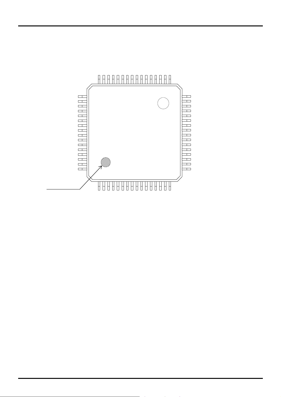
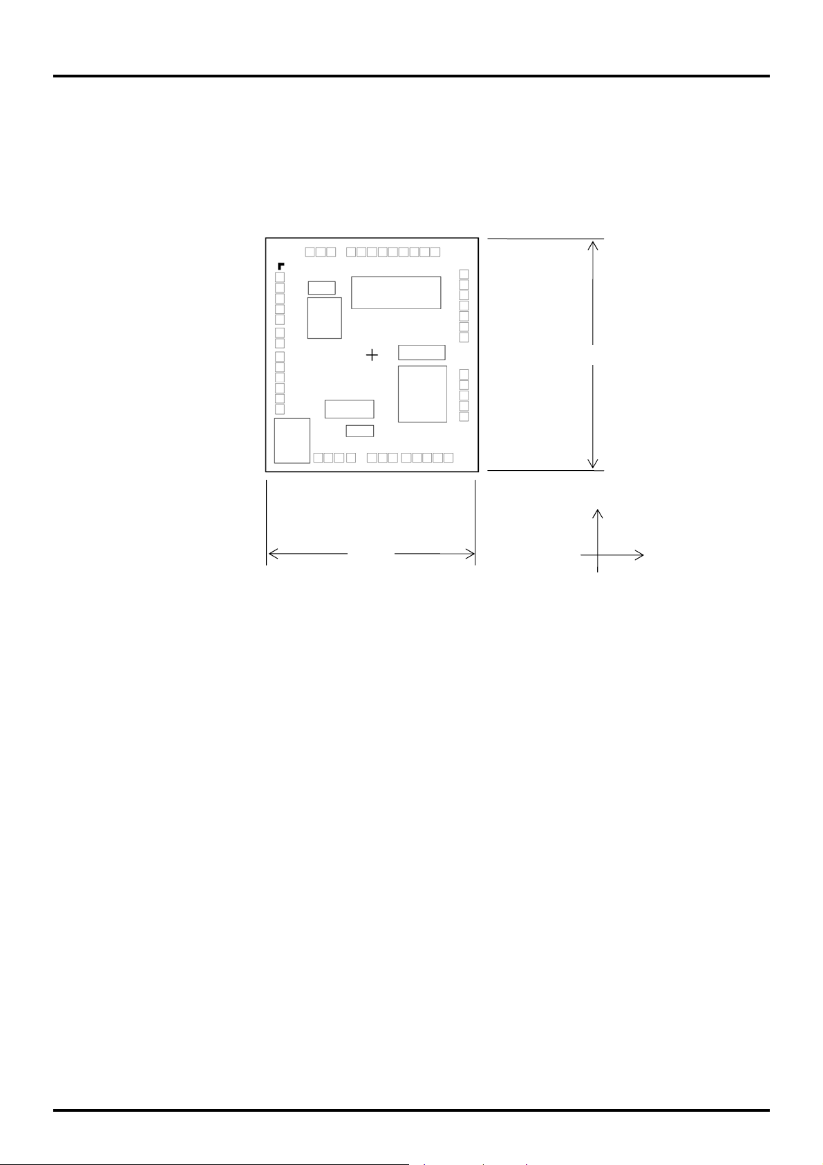
1.3.1.7 Pin Layout of ML610471 Chip
SEG13
SEG12
SEG11
31
32
33
34 P67
P64
P63
P62
P61
P60
P20
P21
P42
P43
P00
P01
P02
P03
37
38
39
40
41
42
43
44
45
46
47
48
49
P65
36
P66
35
SEG10
30
SEG9
29
SEG8
28
SEG7
27
SEG6
26
SEG5
25
SEG4
24
SEG3
23
COM4/SEG2
22
COM3/SEG1
21
COM2/SEG0
20
COM1
19
18
COM0
17
VL3
VL2
16
VL1
15
C2
14
C1
13
1.77mm
8
1 2 3 4 5 6 7
XT0
XT1
VSS
VDD
VDDL
1.61mm
9
11
12
10
P44
P45
P46
P47
P35
TEST0
RESET_N
Y
X
Chip size: 1.61 mm × 1.77 mm
PAD count: 49 pins
Minimum PAD pitch: 80μm
PAD aperture: 70μm×70μm
Chip thickness: 350μm
Voltage of the rear side of chip: V
level.
SS
Figure 1-9 Dimensions of ML610471 Chip
1-12

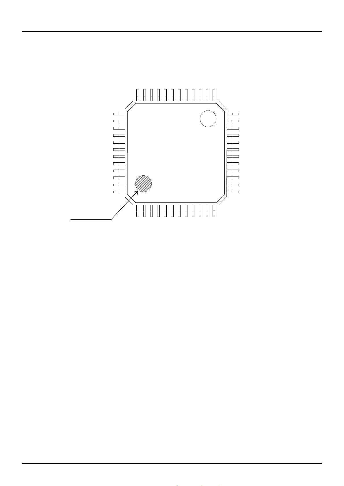
1.3.1.8 Pin Layout of ML610472 Chip
SEG17
P63
P62
P61
P60
P20
P21
P42
P43
P00
P01
P02
P03
37
38
39
40
41
42
43
44
45
46
47
48
49
SEG16
36
SEG15
35
ML610471/472/473/Q471/Q472/Q473 User's Manual
Chapter 1 Overview
SEG13
SEG12
SEG11
SEG10
SEG9
SEG8
SEG7
SEG6
SEG5
31
32
33
34 SEG14
30
29
28
27
26
25
SEG4
24
SEG3
23
COM4/SEG2
22
COM3/SEG1
21
COM2/SEG0
20
COM1
19
18
COM0
17
VL3
VL2
16
VL1
15
C2
14
C1
13
1.77mm
8
1 2 3 4 5 6 7
XT0
XT1
VSS
VDD
VDDL
1.61mm
9
11
12
10
P44
P45
P46
P47
P35
TEST0
RESET_N
Y
X
Chip size: 1.61 mm × 1.77 mm
PAD count: 49 pins
Minimum PAD pitch: 80μm
PAD aperture: 70μm×70μm
Chip thickness: 350μm
Voltage of the rear side of chip: V
level.
SS
Figure 1-10 Dimensions of ML610472 Chip
1-13
ML610471/472/473/Q471/Q472/Q473 User's Manual
Chapter 1 Overview
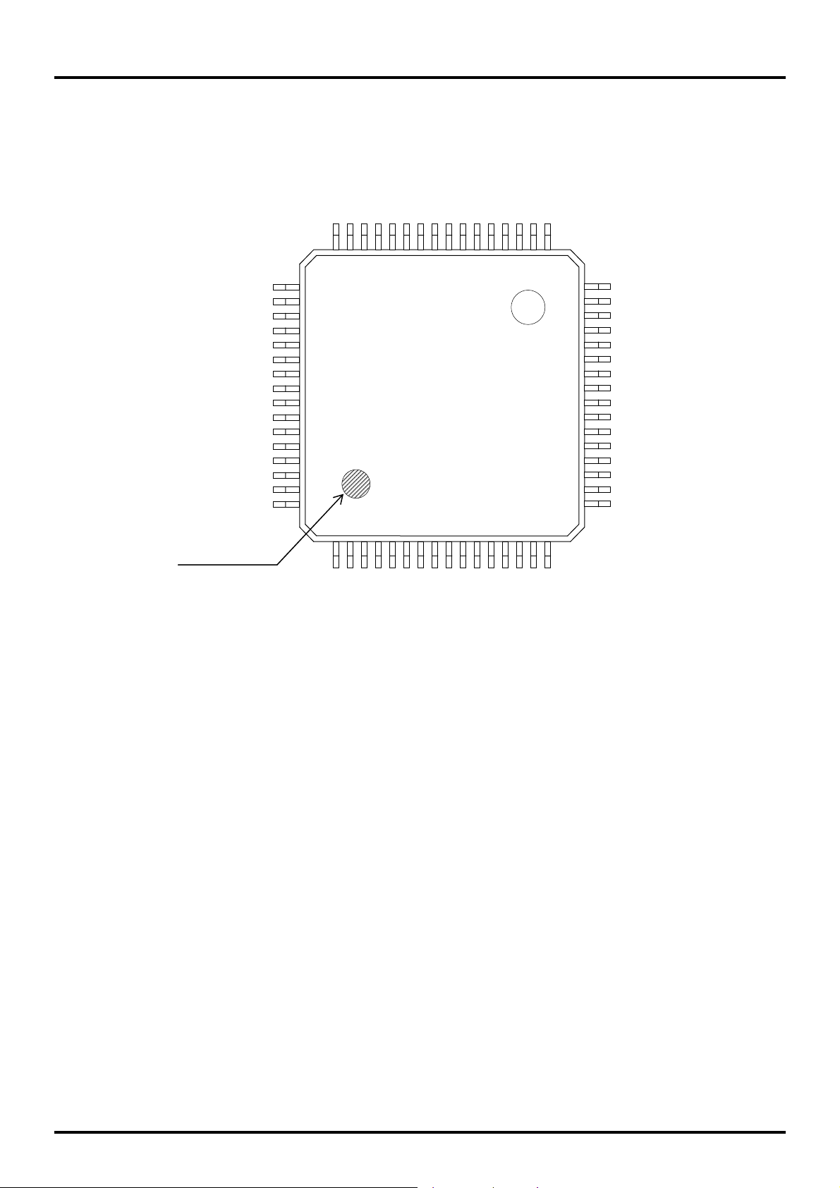
1.3.1.9 Pin Layout of ML610473 Chip
SEG13
SEG12
SEG11
31
32
33
34 SEG14
SEG17
SEG18
SEG19
SEG20
SEG21
P20
P21
P42
P43
P00
P01
P02
P03
37
38
39
40
41
42
43
44
45
46
47
48
49
SEG16
36
SEG15
35
SEG10
30
SEG9
29
SEG8
28
SEG7
27
SEG6
26
SEG5
25
SEG4
24
SEG3
23
COM4/SEG2
22
COM3/SEG1
21
COM2/SEG0
20
COM1
19
18
COM0
17
VL3
VL2
16
VL1
15
C2
14
C1
13
1.77mm
8
1 2 3 4 5 6 7
XT0
XT1
VSS
VDD
VDDL
1.61mm
9
11
12
10
P44
P45
P46
P47
P35
TEST0
RESET_N
Y
X
Chip size: 1.61 mm × 1.77 mm
PAD count: 49 pins
Minimum PAD pitch: 80 μm
PAD aperture: 70 μm×70 μm
Chip thickness: 350 μm
Voltage of the rear side of chip: V
level.
SS
Figure 1-11 Dimensions of ML610473 Chip
1-14
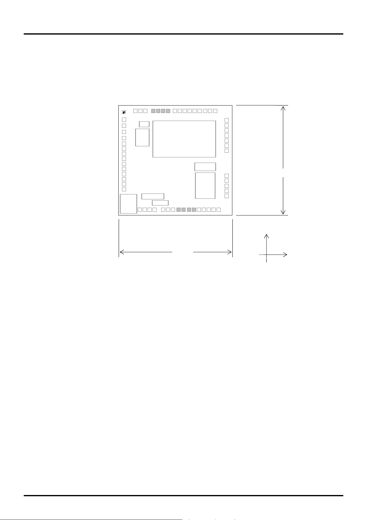
1.3.1.10 Pin Layout of ML610Q471 Chip
P65
P66
36
35
37
P64
P63
38
P62
39
P61
40
P60
41
P20
42
P21
43
P42
44
P43
45
P00
46
P01
47
P02
48
P03
49
VPP
50
ML610471/472/473/Q471/Q472/Q473 User's Manual
Chapter 1 Overview
NC
NC - NC
SEG13
SEG12
SEG11
SEG10
SEG9
SEG8
SEG7
SEG6
28
27
26
SEG5
25
SEG4
24
SEG3
23
COM4/SEG2
22
COM3/SEG1
21
COM2/SEG0
20
COM1
19
18
COM0
VL3
17
VL2
16
VL1
15
C2
14
C1
13
1.88mm
NC
-
-
31
32
34 P67
33
30
29
(NC): No Connection
- NC
- NC
- NC
1 2 3 4 5 6 7
XT0
XT1
VSS
VDD
VDDL
RESET_N
TEST0
1.95mm
- NC
9
8
11
10
12
P44
P45
P46
P47
P35
Chip size: 1.95 mm × 1.88 mm
PAD count: 50 pins
Minimum PAD pitch: 80μm
PAD aperture: 70μm×70μm
Chip thickness: 350μm
Voltage of the rear side of chip: V
SS
Figure 1-12 Dimensions of ML610Q471 Chip
Y
X
level.
1-15
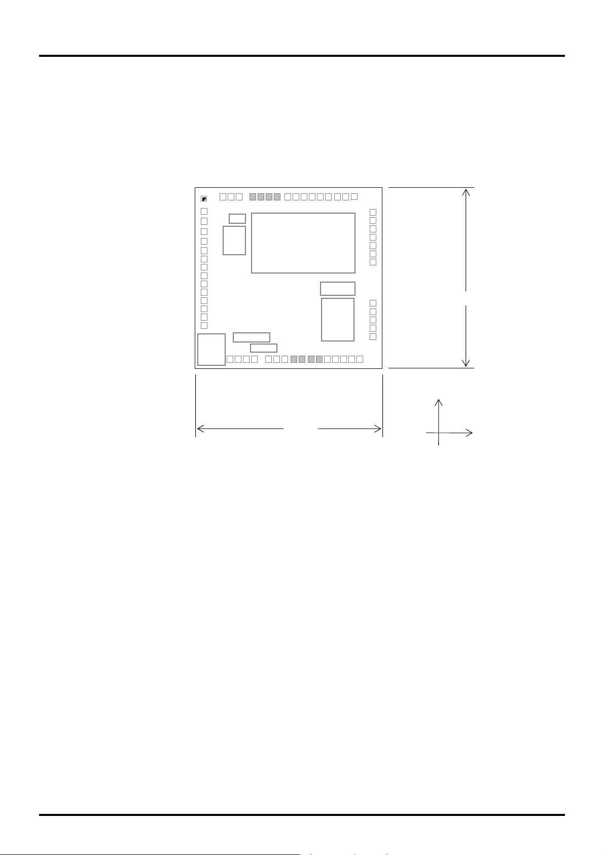
ML610471/472/473/Q471/Q472/Q473 User's Manual
Chapter 1 Overview
1.3.1.11 Pin Layout of ML610Q472 Chip
NC
NC
SEG15
35
NC
-
-
-
34 SEG14
SEG16
36
NC
SEG13
SEG12
SEG11
SEG10
SEG9
SEG8
SEG7
SEG6
31
32
33
30
29
28
27
26
SEG5
25
(NC): No Connection
SEG17
P63
P62
P61
P60
P20
P21
P42
P43
P00
P01
P02
P03
VPP
37
38
39
40
41
42
43
44
45
46
47
48
49
50
- NC
- NC
- NC
1 2 3 4 5 6 7
XT0
VSS
VDD
XT1
VDDL
RESET_N
1.95mm
TEST0
- NC
9
8
11
10
12
P44
P45
P46
P47
P35
Chip size: 1.95 mm × 1.88 mm
PAD count: 50 pins
Minimum PAD pitch: 80μm
PAD aperture: 70μm×70μm
Chip thickness: 350μm
Voltage of the rear side of chip: V
Figure 1-13 Dimensions of ML610Q472 Chip
SEG4
24
SEG3
23
COM4/SEG2
22
COM3/SEG1
21
COM2/SEG0
20
COM1
19
18
COM0
VL3
17
VL2
16
VL1
15
C2
14
C1
13
level.
SS
1.88mm
Y
X
1-16
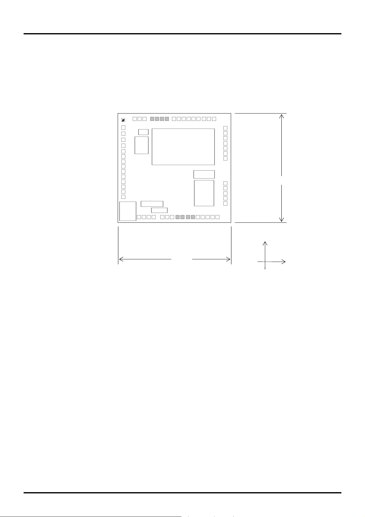
1.3.1.12 Pin Layout of ML610Q473 Chip
SEG16
SEG15
36
35
ML610471/472/473/Q471/Q472/Q473 User's Manual
Chapter 1 Overview
NC
NC
NC
NC
SEG13
SEG12
SEG11
SEG10
SEG9
SEG8
SEG7
SEG6
-
-
-
31
32
34 SEG14
33
30
29
28
27
26
SEG5
25
(NC): No Connection
SEG17
SEG18
SEG19
SEG20
SEG21
P20
P21
P42
P43
P00
P01
P02
P03
VPP
37
38
39
40
41
42
43
44
45
46
47
48
49
50
- NC
- NC
- NC
1 2 3 4 5 6 7
XT0
VSS
VDD
XT1
VDDL
RESET_N
1.95mm
TEST0
- NC
9
8
11
10
12
P44
P45
P46
P47
P35
Chip size: 1.95 mm × 1.88 mm
PAD count: 50 pins
Minimum PAD pitch: 80 μm
PAD aperture: 70 μm×70 μm
Chip thickness: 350 μm
Voltage of the rear side of chip: V
Figure 1-14 Dimensions of ML610Q473 Chip
SEG4
24
SEG3
23
COM4/SEG2
22
COM3/SEG1
21
COM2/SEG0
20
COM1
19
18
COM0
VL3
17
VL2
16
VL1
15
C2
14
C1
13
level.
SS
1.88mm
Y
X
1-17
ML610471/472/473/Q471/Q472/Q473 User's Manual
Chapter 1 Overview
1.3.1.13 Pad Coordinates of ML610471/ML610472/M610473 Chip
Table 1-1 Pad Coordinates of ML610471/ML610472/ML610473
PAD
No.
Pad
Name
1 VDD
2 VSS
3 VDDL
4 XT0
5 XT1
6 RESET_N
7 TEST0
8 P44
9 P45
10 P46
11 P47
12 P35
13 C1
14 C2
15 VL1
16 VL2
17 VL3
18 COM0
19 COM1
20 COM2/SEG0
21 COM3/SEG1
22 COM4/SEG2
23 SEG3
24 SEG4
25 SEG5 480
26 SEG6 400
27 SEG7 320
28 SEG8 240
29 SEG9 160
(*1)
Pad for ML610471 .
(*2)
ML610471/2/3
X (μm)
-410
-330
-250
-160
0
-80
160
260
340
420
500
580
699
699
699
699
699
699
699
699
699
699
699
699
Y (μm)
-779 30 SEG10
-779 31 SEG11
-779 32 SEG12
-779 33 SEG13
-779 P67
-779
-779 P66
-779
-779 P65
-779
-779 P64
-779
-468 P63
-388
-308 P62
-228
-148 P61
133
213 P60
293
373
453
533
613
779
779
779
779
779
Pad for ML610472.
PAD
No.
34
35
36
37
38
39
40
41
42
43
44
45
46
47 P01 -699 -253
48 P02 -699 -333
49 P03
(*3)
Pad for ML610473.
SEG14
SEG15
SEG16
SEG17
SEG18
SEG19
SEG20
SEG21
Pad
Name
(*1)
(*2) (*3)
(*1)
(*2) (*3)
(*1)
(*2) (*3)
(*1)
(*2) (*3)
(*1) (*2)
(*1) (*2)
(*1) (*2)
(*1) (*2)
P20
P21
P42
P43
P00
(*3)
(*3)
(*3)
(*3)
Chip Center: X=0,Y=0
ML610471/2/3
X (μm) Y (μm)
80
0
-80
-160
-310
-390
-470
-699
-699
-699 427
-699 347
-699 267
779
779
779
779
779
779
779
587
507
-699 167
-699 87
-699 -13
-699 -93
-699 -173
-699 -413
1-18

ML610471/472/473/Q471/Q472/Q473 User's Manual
1.3.1.14 Pad Coordinates of ML610Q471/ML610Q472/M610Q473 Chip
Table 1-2 Pad Coordinates of ML610Q471/ML610Q472/ML610Q473
PAD
No.
Pad
Name
1 VDD
2 VSS
3 VDDL
4 XT0
5 XT1
6 RESET_N
7 TEST0
8 P44
9 P45
10 P46
11 P47
12 P35
13 C1
14 C2
15 VL1
16 VL2
17 VL3
18 COM0
19 COM1
20 COM2/SEG0
21 COM3/SEG1
22 COM4/SEG2
23 SEG3
24 SEG4
25 SEG5 650
26 SEG6 570
27 SEG7 490
28 SEG8 410
29 SEG9 330
(*1)
Pad for ML610Q471 .
ML610Q471/2/3
X (μm)
Y (μm)
-580
-500
-420
-330
-170
-90
-10
430
510
590
670
750
869
869
869
869
869
869
869
869
869
869
869
869
(*2)
Pad for ML610Q472.
PAD
No.
Pad
Name
-834 30 SEG10
-834 31 SEG11
-834 32 SEG12
-834 33 SEG13
-834 P67
-834
-834 P66
-834
-834 P65
-834
-834 P64
-834
-523 P63
-443
-363 P62
-283
-203 P61
175
255 P60
335
415
495
575
655
834
834
834
834
834
(*3)
Pad for ML610Q473.
34
35
36
37
38
39
40
41
42
43
44
45
46
47
48
49
50
(*1)
(*2) (*3)
SEG14
(*1)
(*2) (*3)
SEG15
(*1)
(*2) (*3)
SEG16
(*1)
(*2) (*3)
SEG17
(*1) (*2)
(*3)
SEG18
(*1) (*2)
(*3)
SEG19
(*1) (*2)
(*3)
SEG20
(*1) (*2)
(*3)
SEG21
P20
P21
P42
P43
P00
P01 -869 -198
P02 -869 -278
P03
VPP
Chapter 1 Overview
Chip Center: X=0,Y=0
ML610Q471/2/3
X (μm) Y (μm)
250
170
90
10
-480
-560
-640
-869
-869
-869 482
-869 402
-869 322
-869 222
-869 142
-869 42
-869 -38
-869 -118
-869 -358
-869 -438
834
834
834
834
834
834
834
642
562
1-19

ML610471/472/473/Q471/Q472/Q473 User's Manual
Chapter 1 Overview
1.3.2 List of Pins
PIN No. Primary function Secondary function
(*1)
48
64
2 3 2 2 VSS ⎯ Negative power supply pin
1 2 1 1 VDD
3 4 3 3 VDDL
48 63
15 22 15 15 VL1
16 23 16 16 VL2
17 24 17 17 VL3
13 20 13 13 C1
14 21 14 14 C2
7 10 7 7 TEST0 I/O Test pin
6 9 6 6 RESET_N I Reset input pin
4 6 4 4 XT0 I Low-speed clock oscillation pin
5 8 5 5 XT1 O Low-speed clock oscillation pin
44 59 46 46
45 60 47 47
46 61 48 48
47 62 49 49 P03/EXI3 I
42 55 42 42 P20/LED0 O Output port LSCLK O Low-speed clock output
⎯
12 15 12 12 P35 I/O Input/output port RCM O
PAD
No.
(*2)
(MASK)
56 43 43 P21/LED1 O Output port OUTCLK O High-speed clock output
−
PAD
No.
(FLASH)
Pin name I/O Function Pin name I/O Function
(*3)
50 VPP ⎯ Power supply pin for Flash ROM
P00/EXI0/
CAP0
P01/EXI1/
CAP1
P02/EXI2/
RXD0
Positive power supply pin
⎯
Power supply pin for internal
⎯
logic (internally generated)
Power supply pin for LCD bias
(internally generated or
⎯
connected to positive power
supply pin)
Power supply pin for LCD bias
(internally generated or
⎯
connected to positive power
supply pin)
Power supply pin for LCD bias
⎯
(internally generated)
Capacitor connection pin for
⎯
LCD bias generation
Capacitor connection pin for
⎯
LCD bias generation
Input port,
I
External interrupt,
Capture 0 input
Input port,
I
External interrupt,
Capture 1 input
Input port,
I
External interrupt,
UART0 received data
Input port,
External interrupt
(*2)
(*2)
⎯ ⎯ ⎯
⎯ ⎯ ⎯
⎯ ⎯ ⎯
⎯ ⎯ ⎯
⎯ ⎯ ⎯
⎯ ⎯ ⎯
⎯ ⎯ ⎯
⎯ ⎯ ⎯
⎯ ⎯ ⎯
⎯ ⎯ ⎯
⎯ ⎯ ⎯
⎯ ⎯ ⎯
⎯ ⎯ ⎯
⎯ ⎯ ⎯
⎯ ⎯ ⎯
⎯ ⎯ ⎯
⎯ ⎯ ⎯
RC type ADC oscillation
monitor
57 44 44 P42 I/O Input/output port RXD0
⎯
43 58 45 45 P43 I/O Input/output port TXD0 O UART data output
8 11 8 8 P44/ T2CK I/O
9 12 9 9 P45/T3CK I/O
10 13 10 10 P46 I/O Input/output port RS1 O
11 14 11 11 P47 I/O Input/output port RT1 O
(*1)
48pin TQFP.
(*3)
Pad for ML610Q471/ML610Q472/ML610Q473
(*2)
64pin TQFP
Input/output port,
Timer 2 external clock input
Input/output port,
Timer 3 external clock input
IN1 I
CS1 O
UART0 received data
⎯
RC type ADC1 oscillation
input pin
RC type ADC1 reference
capacitor connection pin
RC type ADC1 reference
resistor connection pin
RC type ADC1
measurement resistor
sensor connection pin
1-20

ML610471/472/473/Q471/Q472/Q473 User's Manual
Chapter 1 Overview
PIN No. Primary function Secondary function
(*1)
48
64
(*2)
PAD
(MASK)
18 25 18 18 COM0 O LCD common pin
19 26 19 19 COM1 O LCD common pin
20 27 20 20
21 28 21 21
22 29 22 22
23 30 23 23 SEG3 O LCD segment pin
24 31 24 24 SEG4 O LCD segment pin
25 34 25 25 SEG5 O LCD segment pin
26 35 26 26 SEG6 O LCD segment pin
27 36 27 27 SEG7 O LCD segment pin
28 37 28 28 SEG8 O LCD segment pin
29 38 29 29 SEG9 O LCD segment pin
30 39 30 30 SEG10 O LCD segment pin
31 40 31 31 SEG11 O LCD segment pin
32 41 32 32 SEG12 O LCD segment pin
33 42 33 33 SEG13 O LCD segment pin
34 44 34 34
35 45 35 35
36 46 36 36
37 50 37 37
38 51 38 38
39 52 39 39
40 53 40 40
41 54 41 41
(*1)
48pin TQFP.
(*3)
Pad for ML610Q471/ML610Q472/ML610Q473
(*4)
Pad for ML610471/ML610Q471.
(*5)
Pad for ML610472/ML610Q472.
(*6)
Pad for ML610473/ML610Q473.
No.
(*2)
PAD
No.
(FLASH)
Pin name I/O Function Pin name I/O Function
COM2/
SEG0
COM3/
SEG1
COM4/
SEG2
P67
SEG14
P66
SEG15
P65
SEG16
P64
SEG17
P63
SEG18
P62
SEG19
P61
SEG20
P60
SEG21
64pin TQFP
)
(*6)
(*6)
(*6)
(*4) (*5)
(*4) (*5)
(*4) (*5)
(*4) (*5)
O LCD common/segment pin
O LCD common/segment pin
O LCD common/segment pin
(*4)
(*5)(*6
(*4)
(*4)
(*4)
(*5)
(*5)
(*5)
(*6)
(*6)
(*6)
(*6)
Output port
O
LCD segment pin
Output port
O
LCD segment pin
Output port
O
LCD segment pin
Output port
O
LCD segment pin
Output port
O
LCD segment pin
Output port
O
LCD segment pin
Output port
O
LCD segment pin
Output port
O
LCD segment pin
⎯ ⎯ ⎯
⎯ ⎯ ⎯
⎯ ⎯ ⎯
⎯ ⎯ ⎯
⎯ ⎯ ⎯
⎯ ⎯ ⎯
⎯ ⎯ ⎯
⎯ ⎯ ⎯
⎯ ⎯ ⎯
⎯ ⎯ ⎯
⎯ ⎯ ⎯
⎯ ⎯ ⎯
⎯ ⎯ ⎯
⎯ ⎯ ⎯
⎯ ⎯ ⎯
⎯ ⎯ ⎯
⎯ ⎯ ⎯
⎯ ⎯ ⎯
⎯ ⎯ ⎯
⎯ ⎯ ⎯
⎯ ⎯ ⎯
⎯ ⎯ ⎯
⎯ ⎯ ⎯
⎯ ⎯ ⎯
⎯ ⎯ ⎯
⎯ ⎯ ⎯
⎯ ⎯ ⎯
⎯ ⎯ ⎯
⎯ ⎯ ⎯
⎯ ⎯ ⎯
⎯ ⎯ ⎯
⎯ ⎯ ⎯
1-21

ML610471/472/473/Q471/Q472/Q473 User's Manual
Chapter 1 Overview
1.3.3 Pin Descriptions
Pin name I/O Description
System
RESET_N I Reset input pin. When this pin is set to a “L” level, system reset
mode is set and the internal section is initialized. When this pin is
set to a “H” level subsequently, program execution starts. A pull-up
resistor is internally connected.
XT0 I
XT1 O
LSCLK O Low-speed clock output. Assigned to the secondary function of the
OUTCLK O High-speed clock output pin. This pin is used as the secondary
General-purpose input port
P00 to P03 I General-purpose input port. Primary Positive
General-purpose output port
P20, P21 O General-purpose output port.
General-purpose input/output port
P35 I/O General-purpose input/output port.
P42 to P47 I/O General-purpose input/output port.
P60 to P63 O General-purpose output port.
P64 to P67 O General-purpose output port.
UART
TXD0 O UART data output pin. This pin is used as the secondary function of
RXD0 I UART data input pin. This pin is used as the secondary function
External interrupt
EXI0-3 I External maskable interrupt input pins. Interrupt enable and edge
Crystal connection pin for low-speed clock.
A 32.768 kHz crystal resonator is connected to this pin. Capacitors
C
and CGL are connected across this pin and VSS. (see appendix
DL
C measuring circuit 1)
P20 pin.
function of the P21 pin.
This cannot be used as the general output port when used as the
secondary function.
This cannot be used as the general input/output port when used as
the secondary function.
This cannot be used as the general input/output port when used as
the secondary function.
Incorporated only into
ML610471/610Q471/ML610472/ML610Q472, and not into
ML610473/ML610Q473
Incorporated only into ML610473/ML610Q473, and not into
ML610471/ML610Q471/ML610472/ ML610Q472.
the P43 pin.
of the P42 or the primary function of the P02 pin.
selection can be performed for each bit by software. These pins are
used as the primary functions of the P00 to P03 pins.
Primary/
Secondary
— Negative
— —
— —
Secondary —
Secondary —
Primary Positive
Primary Positive
Primary Positive
Primary Positive
Primary Positive
Secondary Positive
Primary Positive
Primary/
Secondary
Positive/
negative
Logic
1-22

ML610471/472/473/Q471/Q472/Q473 User's Manual
Chapter 1 Overview
Pin name I/O Description
Capture
CAP0 I Primary Positive/
CAP1 I
Timer
T2CK I External clock input pin used for Timer 2. This pin is used as the
T3CK I External clock input pin used for Timer 3. This pin is used as the
LED drive
LED0-1 O N-channel open drain output pins to drive LED. This pin is used as
RC oscillation type A/D converter
RCM O RC oscillation monitor pin. This pin is used as the secondary
IN1 I Oscillation input pin of Channel 1. This pin is used as the secondary
CS1 O Reference capacitor connection pin of Channel 1. This pin is used
RS1 O Reference resistor connection pin of Channel 1. This pin is used as
RT1 O Resistor sensor connection pin for measurement of Channel 1. This
Capture trigger input pins. The value of the time base counter is
captured in the register synchronously with the interrupt edge
selected by software. These pins are used as the primary functions
of the P00 pin(CAP0) and P01 pin(CAP1).
primary function of the P44 pin.
primary function of the P45 pin.
the primary function of the P20 pin and P21 pin.
function of the P35 pin.
function of the P44 pin.
as the secondary function of the P45 pin.
the secondary function of the P46 pin.
pin is used as the secondary function of the P47 pin.
Primary/
Secondary
negative
Primary Positive/
negative
Primary
Primary
Primary Positive
/negative
Secondary
Secondary
Secondary
Secondary
Secondary
Logic
—
—
—
—
—
—
—
1-23

ML610471/472/473/Q471/Q472/Q473 User's Manual
Chapter 1 Overview
Pin name I/O Description
LCD drive signal
COM0 to COM4 O Common output pins. COM2, COM3, and COM4 can be switched
to SEG0, SEG1, and SEG2, respectively, through the register
setting. To change the setting, switch between COM4 and SEG2 for
one pin and switch between COM3, COM4 and SEG1, SEG2 for
two pins.
SEG0 to
SEG13
SEG14 to
SEG17
O Segment output pin. The SEG0, SEG1, and SEG2 pins are for
switching the register setting with the COM2, COM3, and COM4.
O Segment output pin. Incorporated into
ML610472/ML610Q472/ML610473/ML610Q473, not into
ML610471/ML610Q471.
SEG18 to
SEG21
O Segment output pin. Incorporated into ML610473/ML610Q473, not
into ML610471/ML610Q471/ML610472/ML610Q472.
LCD driver power supply
VL1 — — —
VL2
VL3
C1
C2
Power supply pin for LCD bias (internally generated) or power
supply connection pin. Depending on LCD Bias setting and V
—
voltage level, V
—
the connection method, see Chapter 19, "LCD Drivers".
—
Power supply pins for LCD bias (internally generated). Capacitor
C
(see Appendix C measuring circuit 1) is connected between C1
12
—
and C2.
DD
or V
or capacitor is connected. For details of
DDL
DD
Test
TEST0 I/O Pin for testing. A pull-down resistor is internally connected. — Positive
Power supply
VSS — Negative power supply pin. — —
VDD — Positive power supply pin. — —
VDDL — Positive power supply pin (internally generated) for internal logic.
Capacitors C
and C
L0
(see Appendix C measuring circuit 1) are
L1
connected between this pin and VSS.
VPP — Power supply pin for programming Flash ROM. A pull-down resistor
is internally connected.
This pin is only for ML610Q471/ML610Q472/ML610Q473.
Primary/
Secondary
Logic
— —
— —
— —
— —
— —
— —
— —
— —
— —
— —
1-24

1.3.4 Handling of Unused Pins
Table 1-3 shows methods of terminating the unused pins.
Table 1-3 Termination of Unused Pins
Pin Recommended pin handling
VPP Open
VL1 Open
VL2 Open
VL3 Open
C1, C2 Open
RESET_N Open
TEST0 Pull down(1kΩ to VSS)
P00 to P03 VDD or VSS
P20, P21 Open
P35 Open
P42 to P47 Open
P60 to P67 Open
COM0 to COM4 Open
SEG0 to SEG21 Open
Note:
It is recommended to set the unused input ports and input/output ports to the inputs with pull-down resistors/pull-up
resistors or the output mode since the supply current may become excessively large if the pins are left open in the
high impedance input setting.
ML610471/472/473/Q471/Q472/Q473 User's Manual
Chapter 1 Overview
1-25

Chapter 2
CPU and Memory Space

ML610471/472/473/Q471/Q472/Q473 User's Manual
Chapter 2 CPU and Memory Space
2. CPU and Memory Space
2.1 Overview
This LSI includes 8-bit CPU nX-U8/100 and the memory model is SMALL model.
For details of the CPU nX-U8/100, see “nX-U8/100 Core Instruction Manual”.
2.2 Program Memory Space
The program memory space is used to store program codes, table data (ROM window), or vector tables.
The program codes have a length of 16 bits and are specified by a 16-bit program counter (PC).
The ROM window area data has a length of 8 bits and can be used as table data.
The vector table, which has 16-bit long data, can be used as reset vectors, hardware interrupt vectors, and software
interrupt vectors.
The program memory space consists of one segment and has 8-Kbyte (4-Kword) capacity.
Figure 2-1 shows the configuration of the program memory space.
PC
0000H
00FFH
0100H
Vector Table Area
or
Program Code
ROM Window Area
Program Code Area
or
ROM Window Area
1F00H
8bit
1FFFH
Test Data Area
Figure 2-1 Configuration of Program Memory Space
Note:
・The 256 bytes (128 words) from 1F00H to 1FFFH are the test data area.
・The test data area is rewritable but cannot be used as the program code area.
・Set “0FFH” data (BRK instruction) in the unused area of the program memory space.
2-1

ML610471/472/473/Q471/Q472/Q473 User's Manual
Chapter 2 CPU
2.3 Data Memory Space
The data memory space of this LSI consists of the ROM window area, 512Byte RAM area, and SFR area of Segment 0.
The data memory has the 8-bit length and is specified by the addressing specified by each instruction.
Figure 2-2 shows the configuration of the data memory space.
DSR: Data
address Segment 0
0000H
ROM Window
Area
1FFFH
2000H
DFFFH
E000H
E1FFH
E400H
EFFFH
F000H
FFFFH
8bit
Figure 2-2 Configuration of Data Memory Space
Note:
・The contents of the RAM area are undefined at system reset. Initialize this area by software.
・In IDEU8, setting the “Prohibition of __far description/Deterrence of evacuation of DSR in an interruption function”
check box. For details, see “IDEU8 User’s Manual”.
Unused area
RAM area
512 byte
Unused area
SFR Area
2-2

2.4 Instruction Length
The length of an instruction is 16 bits.
2.5 Data Type
The data types supported include byte (8 bits) and word (16 bits).
ML610471/472/473/Q471/Q472/Q473 User's Manual
Chapter 2 CPU and Memory Space
2-3

ML610471/472/473/Q471/Q472/Q473 User's Manual
Chapter 2 CPU
2.6 Description of Registers
2.6.1 List of Registers
Address Name Symbol (Byte) Symbol (Word) R/W Size Initial
0F000H Data segment register DSR — R/W 8 00H
value
2-4

ML610471/472/473/Q471/Q472/Q473 User's Manual
Chapter 2 CPU and Memory Space
2.6.2 Data Segment Register (DSR)
Address: 0F000H
Access: R/W
Access size: 8-bit
Initial value: 00H
7 6 5 4 3 2 1 0
DSR — — — — DSR3 DSR2 DSR1 DSR0
R/W R/W R/W R/W R/W R/W R/W R/W R/W
Initial value 0 0 0 0 0 0 0 0
DSR is a special function register (SFR) to retain a data segment.
Always use this register with the initial state (0). For details of DSR, see “nX-U8/100 Core Instruction Manual”.
[Description of Bits]
• DSR3-DSR0 (bits 3 to 0)
DSR3 DSR2 DSR1 DSR0 Description
0 0 0 0 Initial value
In other than above Prohibited
2-5

Chapter 3
Reset Function

ML610471/472/473/Q471/Q472/Q473 User's Manual
Chapter 3 Reset Function
3. Reset Function
3.1 Overview
This LSI has the five reset functions shown below. If any of the five reset conditions is satisfied, this LSI enters system
reset mode.
• Reset by the RESET_N pin
• Reset by power-on detection
• Reset by the 2
• Software reset by execution of the BRK instruction
3.1.1 Features
• The RESET_N pin has an internal pull-up resistor
• 250 ms, 1 sec, 4 sec, or 16 sec can be selected as the watchdog timer (WDT) overflow period
• Built-in reset status register (RSTAT) indicating the reset generation causes
• Only the CPU is reset by the BRK instruction (neither the RAM area nor the SFR area are reset).
3.1.2 Configuration
Figure 3-1 shows the configuration of the reset generation circuit.
nd
watchdog timer (WDT) overflow
V
RESET_N
Power on reset
WDT reset
R
STAT : Reset status register
Figure 3-1 Configuration of Reset Generation Circuit
3.1.3 List of Pins
Pin name Input/output Function
RESET_N I Reset input pin
RSTAT
RESET
Data bus
3-1

ML610471/472/473/Q471/Q472/Q473 User's Manual
Chapter 3 Reset Function
3.2 Description of Registers
3.2.1 List of Registers
Address Name Symbol (Byte) Symbol (Word) R/W Size
0F001H Reset status register RSTAT — R/W 8 ⎯
3.2.2 Reset Status Register (RSTAT)
Address: 0F001H
Access: R/W
Access size: 8-bit
Initial value: Undefined
7 6 5 4 3 2 1 0
RSTAT ⎯ ⎯ ⎯ ⎯ ⎯ WDTR ⎯ POR
R/W R/W R/W R/W R/W R/W R/W R/W R/W
Initial value 0 0 0 0 0 0 0 1
RSTAT is a special function register (SFR) that indicates the causes by which the reset is generated.
At the occurrence of reset, the contents of RSTAT are not initialized, while the bit indicating the cause of the reset is set
to ”1”. When checking the reset cause using this function, perform write operation to RSTAT in advance and initialize
the contents of RSTAT to “00H”.
[Description of Bits]
• POR (bit 0)
The POR bit is a flag that indicates that the power-on reset is generated. Th is bit is set to “1” when powered on.
POR Description
0 Power-on reset not generated
1 Power-on reset generated
• WDTR (bit 2)
The WSDTR is a flag that indicates that the watchdog timer reset is generated. This bit is set to “1” when the
reset by overflow of the watchdog timer is generated.
WDTR Description
0 Watchdog timer reset not occurred
1 Watchdog timer reset occurred
Note:
No flag is provided that indicates the occurrence of reset by the RESET_N pin.
Initial
value
3-2

ML610471/472/473/Q471/Q472/Q473 User's Manual
Chapter 3 Reset Function
3.3 Description of Operation
3.3.1 Operation of System Reset Mode
System reset has the highest priority among all the processings and any other processing being executed up to then is
cancelled.
The system reset mode is set by any of the following causes.
• Reset by the RESET_N pin
• Reset by power-on detection
• Reset by watchdog timer (WDT) overflow
• Software reset by the BRK instruction (only the CPU is reset)
In system reset mode, the following processing is performed.
(1)The power circuit is initialized. However, it is not initialized by the reset by the BRK instruction execution. For the
details of the power circuit, refer to Chapter 19, “Power Circuit”.
(2)All the special function registers (SFRs) whose initial value is not undefined are initialized. However, the
initialization is not performed by software reset due to execution of the BRK instruction. See Appen dix A
“Registers” for the initial values of the SFRs.
(3)CPU is initialized.
• All the registers in CPU are initialized.
• The contents of addresses 0000H and 0001H in the program memory are set to the stack pointer (SP).
• The contents of addresses 0002H and 0003H in the program memory are set to the program counter (PC).
However, when the interrupt level (ELEVEL) of the program status word (PSW) at reset by the BRK instruction
is 1 or lower, the contents of addresses 0004H and 0005H of the program memory are set in the program counter
(PC). For the BRK instruction, see “nX-U8/100 Core Instruction Manual”.
Note:
In system reset mode, the contents of data memory and those of any SFR whose initial value is undefined are not
initialized and are undefined. Initialize them by software.
In system reset mode by the BRK instruction, no special function register (SFR) that has a fixed initial value is
initialized either. Therefore initialize such an SFR by software.
3-3

Chapter 4
MCU Control Function

ML610471/472/473/Q471/Q472/Q473 User's Manual
Chapter 4 MCU Control Function
4. MCU Control Function
4.1 Overview
The operating states of this LSI are classified into the following 4 modes including system reset mode:
(1) System reset mode
(2) Program run mode
(3) HALT Mode
(4) STOP mode
For system reset mode, see Chapter 3, “Reset Function”.
4.1.1 Features
• HALT mode, where the CPU stops operating and only the peripheral circuit is operating
• STOP mode, where both low-speed oscillation and high-speed oscillation stop
• Stop code acceptor function, which controls transition to STOP mode
• Block control function, which power downs the circuits of unused peripherals (reset registers and stop clock
supplies)
4.1.2 Configuration
Figure 4-1 shows an operating state transition diagram.
Power on
System reset
mode
Reset
STP=”1”
Figure 4-1 Operating State Transition Diagram
Reset
Release reset
Reset or BRK
instruction
External
interrupt
HLT=”1”
Program
operation
mode
Interrupt
HALT Mode STOP mode
4-1

ML610471/472/473/Q471/Q472/Q473 User's Manual
Chapter 4 MCU Control Function
4.2 Description of Registers
4.2.1 List of Registers
Address Name Symbol (Byte) Symbol (Word) R/W Size Initial value
0F008H Stop code acceptor STPACP — W 8 —
0F009H Standby control register SBYCON — W 8 00H
0F028H Block control register 0 BLKCON0 — R/W 8 00H
0F029H Block control register 1 BLKCON1 — R/W 8 00H
0F02AH Block control register 2 BLKCON2 — R/W 8 00H
0F02CH Block control register 4 BLKCON4 — R/W 8 00H
4-2

ML610471/472/473/Q471/Q472/Q473 User's Manual
Chapter 4 MCU Control Function
4.2.2 Stop Code Acceptor (STPACP)
Address: 0F008H
Access: W
Access size: 8-bit
Initial value:—(Undefined)
7 6 5 4 3 2 1 0
STPACP — — — — — — — —
W W W W W W W W W
Initial value - - - - - - - -
STPACP is a write-only special function register (SFR) that is used for setting a STOP mode.
When STPACP is read, “00H” is read.
When data is written to STPACP in the order of “5nH”(n: an arbitrary value) and “0An H”(n : an arbitrary value), the stop
code acceptor is enabled. When the STP bit of the standby control register (SBYCON) is set to “1” in this state, the
mode is changed to the STOP mode. When the STOP mode is set, the STOP code acceptor is disabled.
When another instruction is executed between th e instruction that writes “5nH” to STPACP and the instruction that
writes “0AnH”, the stop code acceptor is enabled after “0AnH” is written. However, if data other than “0AnH” is written
to STPACP after “5nH” is written, the “5nH” write processing becomes invalid so that data must be written again
starting from “5nH”.
During a system reset, the stop code acceptor is disabled.
Note:
The STOP code acceptor cannot be enabled on the condition of that both any interrupt enable flag and the
corresponding interrupt request flag are “1”(An interrupt request occurrence with resetting MIE flag will have the
condition).
4-3

ML610471/472/473/Q471/Q472/Q473 User's Manual
Chapter 4 MCU Control Function
4.2.3 Standby Control Register (SBYCON)
Address: 0F009H
Access: W
Access size: 8-bit
Initial value: 00H
7 6 5 4 3 2 1 0
SBYCON — — — — — — STP HLT
W W W W W W W W W
Initial value 0 0 0 0 0 0 0 0
SBYCON is a special function register (SFR) to control operating mode of MCU.
[Description of Bits]
• STP (bit 1)
The STP bit is used for setting the STOP mode. When the STP bit is set to “1” with the stop code ad apter
enabled by using STPACP, the mode is changed to the STOP mode. When any of the P00 to P04 interrupt
requests enabled by the Interrupt Enable Register 1 (IE1) occurs or an external 8 interrupt request enabled by the
Interrupt Enable Register 2 (IE2) occurs, the STP becomes "0" and the operation returns to the program run
mode.
• HLT (bit 0)
The HALT bit is used for setting a HALT mode. When the HALT bit is set to “1”, the mode is changed to the
HALT mode. When the WDT interrupt request or enabled (the interrupt enable flag is “1”) interrupt request is
issued, the HALT bit is set to “1” and the mode is returned to program run mode.
STP HLT Description
0 0 Program run mode (initial value)
0 1 HALT Mode
1 0 STOP mode
1 1 Prohibited
Note:
The mode cannot be changed to HALT mode or STOP mode on the condition of that both any interrupt enable flag
and the corresponding interrupt request flag are “1”(An interrupt request occurrence with resetting MIE flag will
have the condition).
When a maskable interrupt source (interrupt with enable bit) occurs while the MIE flag of the program status word
(PSW) in the nX-U8/100 core is “0”, the STOP mode and the HALT mode are simply released and interrupt
processing is not performed. For details of PSW, see “nX-U8/100 Core Instruction Manual”.
4-4

ML610471/472/473/Q471/Q472/Q473 User's Manual
Chapter 4 MCU Control Function
4.2.4 Block Control Register 0 (BLKCON0)
Address: 0F028H
Access: R/W
Access size: 8-bit
Initial value: 00H
7 6 5 4 3 2 1 0
BLKCON0 — — — — DTM3 DTM2 — —
R/W R/W R/W R/W R/W R/W R/W R/W R/W
Initial value 0 0 0 0 0 0 0 0
BLKCON0 is a special function register (SFR) to control each block operation.
[Description of Bits]
• DTM2 (bit 2)
The DTM2 bit is used to control Timer 2 operation.
DTM2 Description
0 Enable operating Timer 2 (initial value)
1 Disable operating Timer 2
• DTM3 (bit 3)
The DTM3 bit is used to control Timer 3 operation.
DTM3 Description
0 Enable operating Timer 3 (initial value)
1 Disable operating Timer 3
Note:
•When any flag is set to "1" (disable operation), the function of the applicable block is reset (all registers are
initialized) and the clock supply to such block stops. When this flag is set to "1", the writing to all registers in the
applicable block becomes invalid, and thus the reading fro m such register becomes the initial value. Wh en using th e
function of the applicable block, ensure to reset the applicable flag of this block control register to "0" (enable
operation).
•See Chapter 9, “Timers” for detail about operation of Timer 2 and Timer 3.
4-5

ML610471/472/473/Q471/Q472/Q473 User's Manual
Chapter 4 MCU Control Function
4.2.5 Block Control Register 1 (BLKCON1)
Address: 0F029H
Access: R/W
Access size: 8-bit
Initial value: 00H
7 6 5 4 3 2 1 0
BLKCON1 — DCAPR — — — — — —
R/W R/W R/W R/W R/W R/W R/W R/W R/W
Initial value 0 0 0 0 0 0 0 0
BLKCON1 is a special function register (SFR) to control each block operation.
[Description of Bits]
• DCAPR (bit 6)
The DCAPR bit is used to control Capture operation.
DCAPR Description
0 Enable operating Capture (initial value)
1 Disable operating Capture
Note:
•When any flag is set to "1" (disable operation), the function of the applicable block is reset (all registers are
initialized) and the clock supply to such block stops. When this flag is set to "1", the writing to all registers in the
applicable block becomes invalid, and thus the reading fro m such register becomes the initial value. Wh en using th e
function of the applicable block, ensure to reset the applicable flag of this block control register to "0" (enable
operation).
•See Chapter 8, “Capture” for detail about operation of Capture.
4-6

ML610471/472/473/Q471/Q472/Q473 User's Manual
4.2.6 Block Control Register 2 (BLKCON2)
Address: 0F02AH
Access: R/W
Access size: 8-bit
Initial value: 00H
7 6 5 4 3 2 1 0
BLKCON2 — — — — — DUA0 — —
R/W R/W R/W R/W R/W R/W R/W R/W R/W
Initial value 0 0 0 0 0 0 0 0
BLKCON2 is a special function register (SFR) to control each block operation.
[Description of Bits]
• DUA0 (bit 2)
The DUA0 bit is used to control UART operation.
DUA0 Description
0 Enable operating UART (initial value)
1 Disable operating UART
Note:
•When any flag is set to "1" (disable operation), the function of the applicable block is reset (all registers are
initialized) and the clock supply to such block stops. When this flag is set to "1", the writing to all registers in the
applicable block becomes invalid, and thus the reading fro m such register becomes the initial value. Wh en using th e
function of the applicable block, ensure to reset the applicable flag of this block control register to "0" (enable
operation).
•See Chapter 11, “UART” for detail about operation of UART.
Chapter 4 MCU Control Function
4-7

ML610471/472/473/Q471/Q472/Q473 User's Manual
Chapter 4 MCU Control Function
4.2.7 Block Control Register 4 (BLKCON4)
Address: 0F02CH
Access: R/W
Access size: 8-bit
Initial value: 00H
7 6 5 4 3 2 1 0
BLKCON4 — DLCD — — — — DRAD —
R/W R/W R/W R/W R/W R/W R/W R/W R/W
Initial value 0 0 0 0 0 0 0 0
BLKCON4 is a special function register (SFR) to control each block operation.
[Description of Bits]
• DRAD (bit 1)
The DRAD bit is used to control the RC oscillation type A/D converter operation.
DRAD Description
0 Enable operating RC oscillation type A/D converter (initial value)
1 Disable operating RC oscillation type A/D converter
• DLCD (bit 6)
The DLCD bit is used to control LCD driver operation.
DLCD Description
0 Enable operating LCD driver (initial value)
1 Disable operating LCD driver
Note:
•When any flag is set to "1" (disable operation), the function of the applicable block is reset (all registers are
initialized) and the clock supply to such block stops. When this flag is set to "1", the writing to all registers in the
applicable block becomes invalid, and thus the reading fro m such register becomes the initial value. Wh en using th e
function of the applicable block, ensure to reset the applicable flag of this block control register to "0" (enable
operation).
•See Chapter 19, “LCD Driver” for detail about operation of LCD driver.
•See Chapter 18, “RC Oscillation Type A/D Converter” for detail about operation of RC oscillation type A/D
converter.
4-8

ML610471/472/473/Q471/Q472/Q473 User's Manual
K
T
ode
Chapter 4 MCU Control Function
4.3 Description of Operation
4.3.1 Program Run Mode
The program run mode is the state where the CPU executes instructions sequentially.
At power-on reset, low-speed oscillation stop detect reset, WDT overflow reset, or RESET_N pin reset, the CPU
executes instructions from the addresses that are set in addresses 0002H and 0003H of program memory (ROM) after the
system reset mode is released.
At reset by the BRK instruction, the CPU executes instructions from the addresses that are set in the addresses 0004H
and 0005H of the program memory after the system reset mode is released. However, when the value of the interrupt
level bit (ELEVEL) of the program status word (PSW) is 02H or higher at execution of the BRK instruction (after the
occurrence of the WDT interrupt), the CPU executes instructions from the addresses that are set in the addresses 0002H
and 0003H.
For details of the BRK instruction and PSW, see the “nX-U8/100 Core Instruction Manual” and for the reset function,
see Chapter 3, “Reset Function”.
4.3.2 HALT Mode
The HALT mode is the state where the CPU interrupts execution of instructions and only the peripheral circuits are
running.
When the HLT bit of the standby control register (SBYCON) is set to “1”, the HALT mode is set.
When a WDT interrupt request, or an interrupt request enabled by an interrupt enable register (IE1–IE7) is issued, the
HLT bit is set to “0” on the falling edge of the next system clock (SYSCLK) and the HALT mode is returned to the
program run mode released.
Figure 4-2 shows the operation waveforms in HALT mode.
System clock
システムクロック
SYSCLK
CPUCL
SBYCON.HL
Interrupt request
割込み要求
Program run mode
プログラム動作モード HALT モード
HALT m
Program run mode
プログラム動作モード
Figure 4-2 Operation Waveforms in HALT Mode
Note:
Since up to two instructions are executed during the period between HALT mode release and a transition to interrupt
processing, place two NOP instructions next to the instruction that sets the HLT bit to “1”.
4-9

ML610471/472/473/Q471/Q472/Q473 User's Manual
Chapter 4 MCU Control Function
4.3.3 STOP mode
The STOP mode is the state where low-speed oscillation and high-speed oscillation stop and the CPU and peripheral
circuits stop the operation.
When the stop code acceptor is enabled by writing “5nH”(n: an arbitrary value) and “0AnH”(n: an arbitrary value) to the
stop code acceptor (STPACP) sequentially and the STP bit of the standby control register (SBYCON) is set to “1”, the
STOP mode is entered. When the STOP mode is set, the STOP code acceptor is disabled.
When any of the P00 to P03 interrupt requests occurs with th e interrupt enabled (the interrupt enable flag is "1"), the
STP bit is set to "0", the STOP mode is released, and the mode is returned to the program run mode.
4.3.3.1 STOP Mode When CPU Operates with Low-Speed Clock
When the stop code acceptor is in the enabled state and the STP bit of SBYCON is set to “1”, the STOP mode is entered,
stopping low-speed oscillation and high-speed oscillation.
When any of the P00 to P03 interrupt request occurs with the interrupt enabled (interrupt enabled flag is "1") state, the
STP bit becomes "0" and the low-speed oscillation resumes. If the high-speed clock was oscillating before the STOP
mode is entered, the high-speed oscillation restarts. When the high-speed clo ck was not oscillating before the STOP
mode is entered, high-speed oscillation does not start.
When an interrupt request occurs, the STOP mode is released after the elapse of the low-speed oscillatio n start time
) and the low-speed clock (LSCLK) oscillation stabilization time (8192-pulse count), the mode is returned to the
(T
XTL
program run mode, and the low-speed clock (LSCLK) restarts supply to the peripheral circuits. If the high-speed clock
already started oscillation at this time, the high-speed clocks (OSCLK and HSCLK) also restart supply to the peripheral
circuits.
For the low-speed oscillation start time (T
Figure 4-3 shows the operation waveforms in STOP mode when CPU operates with the low-speed clock.
Low-speed
oscillation waveform
), see Appendix C, “Electrical Characteristics”.
XTL
Hiz
T
oscillation
waveform
XTL
High-speed oscillation
SBYCON.STP bit
Figure 4-3 Operation Waveforms in STOP Mode When CPU Operates with Low-Speed Clock
LSCLK
SYSCLK
waveform
HSCLK
Interrupt
request
Low-speed
oscillation
8192 counts
oscillation waveform
High-speed
HSCLK
Program run mode STOP mode Program run mode
oscillation
Maximum 1
count
High-speed
oscillation
16 counts
oscillation waveform
HSCLK waveform
4-10

ML610471/472/473/Q471/Q472/Q473 User's Manual
Low-
Chapter 4 MCU Control Function
4.3.3.2 STOP Mode When CPU Operates with High-Speed Clock
When the CPU is operating with the high-speed clock and the STP bit of SBYCON is set to “1” with the stop code
acceptor enabled, the STOP mode is entered and high-speed oscillation and low-speed oscillation stop.
When any of the P00 to P03 interrupt request occurs with the interrupt enabled (interrupt enabled flag is "1") state, the
STP bit becomes "0" and the high-speed and low-speed oscillatio n resumes.
When an interrupt request is issued, the STOP mode is released after the elapse of the high-speed oscillation start time
) and the high-speed clock (OSCLK) oscillation stabilization time (16-pulse count), the mode is returned to the
(T
RC
program run mode, and the high-speed clocks (OSCLK and HSCLK) restart supply to the peripheral circuits.
The low-speed clock (LSCLK) restarts supply to the peripheral circuits after the elapse of the low-speed oscillation start
time (T
For the high-speed oscillation start time (T
Characteristics” Section in Appendix C.
Figure 4-4 shows the operation waveforms in STOP mode when CPU operates with the high-speed clock.
) and low-speed clock (LSCLK) oscillation stabilization time (8192 count).
XTL
) and low-speed oscillation start time (T
XTH
), see the “Electrical
XTL
High-speed oscillation
waveform
OSCLK
SYSCLK, HSCLK
Low-speed oscillation
waveform
LSCLK
SBYCON.STP bit
Interrupt
request
OSCLK waveform
SYSCLK,HSCLK waveform
Program run mode
TRC
Hiz
speed
oscillation
Maximum 1
count
STOP mode
T
XTL
High-speed oscillation waveform High-speed oscillation waveform
OSCLK waveform
High-speed oscillation 16 counts
SYSCLK,HSCLK
Low-speed
8192 counts
Program run mode
Figure 4-4 Operation Waveforms in STOP Mode When CPU Operates with High-Speed Clock
Note:
Since up to two instructions are executed during the period between STOP mode release and a transition to interrupt
processing, place two NOP instructions next to the instruction that sets the STP bit to “1”.
4-11

ML610471/472/473/Q471/Q472/Q473 User's Manual
Chapter 4 MCU Control Function
4.3.4 Note on Return Operation from STOP/HALT Mode
The operation of returning from the STOP mode and HALT mode varies according to the interrupt level (ELEVEL) of
the program status word (PSW), master interrupt enable flag (MIE), the contents of the interrupt enable register (IE0 to
IE3), and whether the interrupt is a non-maskable interrupt or a maskable interrupt.
For details of PSW and the IE and IRQ registers, see “nX-U8/100 Core Instruction Manual” and Chapter 5, “Interrupt”,
respectively.
Table 4-1 and Table 4-2 show the return operations from STOP/HALT mode.
Table 4-1 Return Operation from STOP/HALT Mode (Non-Maskable Interrupt)
ELEVEL MIE IEn.m IRQn.m Return operation from STOP/HALT mode
* * — 0 Not returned from STOP/HALT mode.
After the mode is returned from STOP/HALT mode, the program
3 * — 1
0,1,2 * — 1
Table 4-2 Return Operation from STOP/HALT Mode (Maskable Interrupt)
ELEVEL MIE IEn.m IRQn.m Return operation from STOP/HALT mode
* * * 0
* * 0 1
* 0 1 1
2,3 1 1 1
0,1 1 1 1
Note:
•If the ELEVEL bit is 0H, it indicates that the CPU is performing neither non-maskable interrupt processing nor
maskable interrupt processing nor software interrupt processing.
•If the ELEVEL bit is 1H, it indicates that the CPU is performing maskable interrupt processing or software interrupt
processing. (ELEVEL is set during interrupt transition cycle.)
•If the ELEVEL bit is 2H, it indicates that the CPU is performing non-maskable interrupt processing. (ELEVEL is set
during interrupt transition cycle.)
•If the ELEVEL bit is 3H, it indicates that the CPU is performing interrupt processing specific to the emulator. This
setting is not allowed in normal applications.
operation restarts from the instruction following the instruction that
sets the STP/HLT bit to “1”. The program operation does not go to the
interrupt routine.
After the mode is returned from the STOP/HALT mode, program
operation restarts from the instruction following the instruction that
sets the STP/HLT bit to “1”, then goes to the interrupt routine.
Not returned from STOP/HALT mode.
After the mode is returned from STOP/HALT mode, the program
operation restarts from the instruction following the instruction that
sets the STP/HLT bit to “1”. The program operation does not go to the
interrupt routine.
After the mode is returned from the STOP/HALT mode, program
operation restarts from the instruction following the instruction that
sets the STP/HLT bit to “1”, then goes to the interrupt routine.
4-12

ML610471/472/473/Q471/Q472/Q473 User's Manual
Chapter 4 MCU Control Function
4.3.5 Block Control Function
This LSI has a block control function, which resets and completely turns operating circuits of unused peripherals off to
make even more reducing current consumption.
For each block control register, the initial value of each flag is "0", meaning the operation of each block is enabled. When
any flag is set to "1" (Disable Operating), the function of the applicable block is reset and the clock supply to this block is
stopped. When this flag is set to "1", the writing to all registers in the applicable block becomes invalid, and thus the
reading from such register becomes the initial value. When using the function o f the applicable block, ensure to reset the
applicable flag of this block control register to "0" (enable operation).
・ BLKCON0 register: Controls (enables/disables) the operation of the Timers 2 and 3 circuits.
・ BLKCON1 register: Controls (enables/disables) the operation of the Capture circuit.
・ BLKCON2 register: Controls (enables/disables) the operation of the UART0 circuit.
・ BLKCON4 register: Controls (disables/enables) the operation of the LCD driver and RC oscillation type A/D
converter circuits.
4-13

Chapter 5
Interrupts

ML610471/472/473/Q471/Q472/Q473 User's Manual
Chapter 5 Interrupt
5. Interrupts
5.1 Overview
This LSI has 13 interrupt sources (External interrupts: 4 sources, Internal interrupts: 9 sources) and a software interrupt
(SWI).
For details of each interrupt, see the following chapters:
Chapter 7, “Time Base Counter”
Chapter 9, “Timer”
Chapter 10, “Watchdog Timer”
Chapter 11, “UART”
Chapter 12, “Port 0”
Chapter 17, “RC Oscillation Type A/D Converter”
5.1.1 Features
• Non-maskable interrupt source: 1 (Internal sources: 1)
• Maskable interrupt sources: 12 (Internal sources: 8 , External sources: 4)
• Software interrupt (SWI): maximum 64 sources
• External interrupts allow edge selection and sampling selection
5-1

ML610471/472/473/Q471/Q472/Q473 User's Manual
Chapter 5 Interrupt
5.2 Description of Registers
5.2.1 List of Registers
Address Name Symbol (Byte) Symbol (Word) R/W Size Initial value
0F011H Interrupt enable register 1 IE1 — R/W 8 00H
0F014H Interrupt enable register 4 IE4 — R/W 8 00H
0F015H Interrupt enable register 5 IE5 — R/W 8 00H
0F016H Interrupt enable register 6 IE6 — R/W 8 00H
0F017H Interrupt enable register 7 IE7 — R/W 8 00H
0F018H Interrupt request register 0 IRQ0 — R/W 8 00H
0F019H Interrupt request register 1 IRQ1 — R/W 8 00H
0F01CH Interrupt request register 4 IRQ4 — R/W 8 00H
0F01DH Interrupt request register 5 IRQ5 — R/W 8 00H
0F01EH Interrupt request register 6 IRQ6 — R/W 8 00H
0F01FH Interrupt request register 7 IRQ7 — R/W 8 00H
5-2

ML610471/472/473/Q471/Q472/Q473 User's Manual
(
(
(
(
Chapter 5 Interrupt
5.2.2 Interrupt Enable Register 1 (IE1)
Address: 0F011H
Access: R/W
Access size: 8-bit
Initial value: 00H
7 6 5 4 3 2 1 0
IE1 — — — — EP03 EP02 EP01 EP00
R/W R/W R/W R/W R/W R/W R/W R/W R/W
Initial value 0 0 0 0 0 0 0 0
IE1 is a special function register (SFR) to control enable/disable for each interrupt request.
When an interrupt is accepted, the master interrupt enable flag (MIE) is set to “0”, but the corresponding flag of IE1 is
not reset.
[Description of Bits]
• EP00 (bit 0)
EP00 is the enable flag for the input port P00 pin interrupt (P00INT).
EP00 Description
0 Disabled
1 Enabled
• EP01 (bit 1)
EP01 is the enable flag for the input port P01 pin interrupt (P01INT).
EP01 Description
0 Disabled
1 Enabled
• EP02 (bit 2)
EP02 is the enable flag for the input port P02 pin interrupt (P02INT).
EP02 Description
0 Disabled
1 Enabled
• EP03 (bit 3)
EP03 is the enable flag for the input port P03 pin interrupt (P03INT).
EP03 Description
0 Disabled
1 Enabled
initial value)
initial value)
initial value)
initial value)
5-3

ML610471/472/473/Q471/Q472/Q473 User's Manual
(
(
Chapter 5 Interrupt
5.2.3 Interrupt Enable Register 4 (IE4)
Address: 0F014H
Access: R/W
Access size: 8-bit
Initial value: 00H
7 6 5 4 3 2 1 0
IE4 — — ERAD — — — — EUA0
R/W R/W R/W R/W R/W R/W R/W R/W R/W
Initial value 0 0 0 0 0 0 0 0
IE4 is a special function register (SFR) to control enable/disable for each interrupt request.
When an interrupt is accepted, the master interrupt enable flag (MIE) is set to “0”, but the corresponding flag of IE4 is
not reset.
[Description of Bits]
• EUA0 (bit 0)
EUA0 is the enable flag for the UART0 interrupt (UA0INT).
EUA0 Description
0 Disabled
1 Enabled
• ERAD (bit 5)
ERAD is the enable flag for the RC oscillation type A/D converter interrupt (RADINT).
ERA0 Description
0 Disabled
1 Enabled
initial value)
initial value)
5-4

ML610471/472/473/Q471/Q472/Q473 User's Manual
(
(
Chapter 5 Interrupt
5.2.4 Interrupt Enable Register 5 (IE5)
Address: 0F015H
Access: R/W
Access size: 8-bit
Initial value: 00H
7 6 5 4 3 2 1 0
IE5 — — ETM3 ETM2 — — — —
R/W R/W R/W R/W R/W R/W R/W R/W R/W
Initial value 0 0 0 0 0 0 0 0
IE5 is a special function register (SFR) to control enable/disable for each interrupt request.
When an interrupt is accepted, the master interrupt enable flag (MIE) is set to “0”, but the corresponding flag of IE5 is
not reset.
[Description of Bits]
• ETM2 (bit 4)
ETM2 is the enable flag for the timer 2 interrupt (TM2INT).
ETM2 Description
0 Disabled
1 Enabled
• ETM3 (bit 5)
ETM3 is the enable flag for the timer 3 interrupt (TM3INT).
ETM3 Description
0 Disabled
1 Enabled
initial value)
initial value)
5-5

ML610471/472/473/Q471/Q472/Q473 User's Manual
(
(
Chapter 5 Interrupt
5.2.5 Interrupt Enable Register 6 (IE6)
Address: 0F016H
Access: R/W
Access size: 8-bit
Initial value: 00H
7 6 5 4 3 2 1 0
IE6 E32H — E128H — — — — —
R/W R/W R/W R/W R/W R/W R/W R/W R/W
Initial value 0 0 0 0 0 0 0 0
IE6 is a special function register (SFR) to control enable/disable for each interrupt request.
When an interrupt is accepted, the master interrupt enable flag (MIE) is set to “0”, but the corresponding flag of IE6 is
not reset.
[Description of Bits]
• E128H (bit 5)
E128H is the enable flag for the time base counter 128 Hz interrupt (T128HINT).
E128H Description
0 Disabled
1 Enabled
• E32H (bit 7)
E32H is the enable flag for the time base counter 32 Hz interrupt (T32HINT).
E32H Description
0 Disabled
1 Enabled
initial value)
initial value)
5-6

ML610471/472/473/Q471/Q472/Q473 User's Manual
(
(
Chapter 5 Interrupt
5.2.6 Interrupt Enable Register 7 (IE7)
Address: 0F017H
Access: R/W
Access size: 8-bit
Initial value: 00H
7 6 5 4 3 2 1 0
IE7 — — — — E2H — — E16H
R/W R/W R/W R/W R/W R/W R/W R/W R/W
Initial value 0 0 0 0 0 0 0 0
IE7 is a special function register (SFR) to control enable/disable for each interrupt request.
When an interrupt is accepted, the master interrupt enable flag (MIE) is set to “0”, but the corresponding flag of IE7 is
not reset.
[Description of Bits]
• E16H (bit 0)
E16H is the enable flag for the time base counter 16 Hz interrupt (T16HINT).
E16H Description
0 Disabled
1 Enabled
• E2H (bit 3)
E2H is the enable flag for the time base counter 2 Hz interrupt (T2HINT).
E2H Description
0 Disabled
1 Enabled
initial value)
initial value)
5-7

ML610471/472/473/Q471/Q472/Q473 User's Manual
)
Chapter 5 Interrupt
5.2.7 Interrupt Request Register 0 (IRQ0)
Address: 0F018H
Access: R/W
Access size: 8-bit
Initial value: 00H
7 6 5 4 3 2 1 0
IRQ0 — — — — — — — QWDT
R/W R/W R/W R/W R/W R/W R/W R/W R/W
Initial value 0 0 0 0 0 0 0 0
IRQ0 is a special function register (SFR) to request an interrupt for each interrupt source.
The watchdog timer interrupt (WDTINT) is a non-maskable interrupt that do not depend on MIE. In this case, an
interrupt is requested to the CPU regardless of the value of the Mask Interrupt Enable flag (MIE).
Each IRQ0 request flag is set to “1” regardless of the MIE value when an interrupt is generated . By setting the IRQ0
request flag to “1” by software, an interrupt can be generated.
The corresponding flag of IRQ0 is set to “0” by hardware when the interrupt request is accepted by the CPU.
[Description of Bits]
• QWDT (bit 0)
QWDT is the request flag for the watchdog timer interrupt (WDTINT).
QWDT Description
0 No request (initial value
1 Request
Note:
When an interrupt is generated by the write instruction to the interrupt requ est register (IRQ0), the interrupt shift
cycle starts after the next 1 instruction is executed.
5-8

ML610471/472/473/Q471/Q472/Q473 User's Manual
)
)
)
)
Chapter 5 Interrupt
5.2.8 Interrupt Request Register 1 (IRQ1)
Address: 0F019H
Access: R/W
Access size: 8-bit
Initial value: 00H
7 6 5 4 3 2 1 0
IRQ1 — — — — QP03 QP02 QP01 QP00
R/W R/W R/W R/W R/W R/W R/W R/W R/W
Initial value 0 0 0 0 0 0 0 0
IRQ1 is a special function register (SFR) to request an interrupt for each interrupt source.
Each IRQ1 request flag is set to “1” regardless of the IE1 and MIE values when an interrupt is generated. In this case, an
interrupt is requested to the CPU when the related flag of the interrupt enable register (IE1) is set to “1” and the master
interrupt enable flag (MIE) is set to “1”.
By setting the IRQ1 request flag to “1” by software, an interrupt can be generated.
The corresponding flag of IRQ1 is set to “0” by hardware when the interrupt request is accepted by the CPU.
[Description of Bits]
• QP00 (bit 0)
QP00 is the request flag for the input port P00 pin interrupt (P00INT).
QP00 Description
0 No request (initial value
1 Request
• QP01 (bit 1)
QP01 is the request flag for the input port P01 pin interrupt (P01INT).
QP01 Description
0 No request (initial value
1 Request
• QP02 (bit 2)
QP02 is the request flag for the input port P02 pin interrupt (P02INT).
QP02 Description
0 No request (initial value
1 Request
• QP03 (bit 3)
QP03 is the request flag for the input port P03 pin interrupt (P03INT).
QP03 Description
0 No request (initial value
1 Request
Note:
When an interrupt is generated by the write instruction to the interrupt requ est register (IRQ1) or to the interrupt
enable register (IE1), the interrupt shift cycle starts after the next 1 instruction is executed.
5-9

ML610471/472/473/Q471/Q472/Q473 User's Manual
)
)
Chapter 5 Interrupt
5.2.9 Interrupt Request Register 4 (IRQ4)
Address: 0F01CH
Access: R/W
Access size: 8-bit
Initial value: 00H
7 6 5 4 3 2 1 0
IRQ4 — — QRAD — — — — QUA0
R/W R/W R/W R/W R/W R/W R/W R/W R/W
Initial value 0 0 0 0 0 0 0 0
IRQ4 is a special function register (SFR) to request an interrupt for each interrupt source.
Each IRQ4 request flag is set to “1” regardless of the IE4 and MIE values when an interrupt is generated. In this case, an
interrupt is requested to the CPU when the related flag of the interrupt enable register (IE4) is set to “1” and the master
interrupt enable flag (MIE) is set to “1”.
By setting the IRQ4 request flag to “1” by software, an interrupt can be generated.
The corresponding flag of IRQ4 is set to “0” by hardware when the interrupt request is accepted by the CPU.
[Description of Bits]
• QUA0 (bit 0)
QUA0 is the request flag for the UART0 interrupt (UA0INT).
QUA0 Description
0 No request (initial value
1 Request
• QRA0 (bit 5)
QMD0 is the request flag for the RC oscillation type A/D converter interrupt (RADINT).
QRA0 Description
0 No request (initial value
1 Request
Note:
When an interrupt is generated by the write instruction to the interrupt requ est register (IRQ4) or to the interrupt
enable register (IE4), the interrupt shift cycle starts after the next 1 instruction is executed.
5-10

ML610471/472/473/Q471/Q472/Q473 User's Manual
)
)
Chapter 5 Interrupt
5.2.10 Interrupt Request Register 5 (IRQ5)
Address: 0F01DH
Access: R/W
Access size: 8-bit
Initial value: 00H
7 6 5 4 3 2 1 0
IRQ3 — — QTM3 QTM2 — — — —
R/W R/W R/W R/W R/W R/W R/W R/W R/W
Initial value 0 0 0 0 0 0 0 0
IRQ5 is a special function register (SFR) to request an interrupt for each interrupt source.
Each IRQ5 request flag is set to “1” regardless of the IE3 and MIE values when an interrupt is generated. In this case, an
interrupt is requested to the CPU when the related flag of the interrupt enable register (IE5) is set to “1” and the master
interrupt enable flag (MIE) is set to “1”.
By setting the IRQ5 request flag to “1” by software, an interrupt can be generated.
The corresponding flag of IRQ5 is set to “0” by hardware when the interrupt request is accepted by the CPU.
[Description of Bits]
• QTM2 (bit 4)
QTM2 is the request flag for the timer 2 interrupt (TM2INT).
QTM2 Description
0 No request (initial value
1 Request
• QTM3 (bit 5)
QTM3 is the request flag for the timer 3 interrupt (TM3INT).
QTM3 Description
0 No request (initial value
1 Request
Note:
When an interrupt is generated by the write instruction to the interrupt requ est register (IRQ5) or to the interrupt
enable register (IE5), the interrupt shift cycle starts after the next 1 instruction is executed.
5-11

ML610471/472/473/Q471/Q472/Q473 User's Manual
)
)
Chapter 5 Interrupt
5.2.11 Interrupt Request Register 6 (IRQ6)
Address: 0F01EH
Access: R/W
Access size: 8-bit
Initial value: 00H
7 6 5 4 3 2 1 0
IRQ6 Q32H — Q128H — — — — —
R/W R/W R/W R/W R/W R/W R/W R/W R/W
Initial value 0 0 0 0 0 0 0 0
IRQ6 is a special function register (SFR) to request an interrupt for each interrupt source.
Each IRQ6 request flag is set to “1” regardless of the IE6 and MIE values when an interrupt is generated. In this case, an
interrupt is requested to the CPU when the related flag of the interrupt enable register (IE6) is set to “1” and the master
interrupt enable flag (MIE) is set to “1”.
By setting the IRQ6 request flag to “1” by software, an interrupt can be generated.
The corresponding flag of IRQ6 is set to “0” by hardware when the interrupt request is accepted by the CPU.
[Description of Bits]
• Q128H (bit 5)
Q128H is the request flag for the time base counter 128 Hz interrupt (T128HINT).
Q128H Description
0 No request (initial value
1 Request
• Q32H (bit 7)
Q32H is the request flag for the time base counter 32 Hz interrupt (T32HINT).
Q32H Description
0 No request (initial value
1 Request
Note:
When an interrupt is generated by the write instruction to the interrupt requ est register (IRQ6) or to the interrupt
enable register (IE6), the interrupt shift cycle starts after the next 1 instruction is executed.
5-12

ML610471/472/473/Q471/Q472/Q473 User's Manual
)
)
Chapter 5 Interrupt
5.2.12 Interrupt Request Register 7 (IRQ7)
Address: 0F01FH
Access: R/W
Access size: 8-bit
Initial value: 00H
7 6 5 4 3 2 1 0
IRQ7 — — — — Q2H — — Q16H
R/W R/W R/W R/W R/W R/W R/W R/W R/W
Initial value 0 0 0 0 0 0 0 0
IRQ7 is a special function register (SFR) to request an interrupt for each interrupt source.
Each IRQ7 request flag is set to “1” regardless of the IE7 and MIE values when an interrupt is generated. In this case, an
interrupt is requested to the CPU when the related flag of the interrupt enable register (IE7) is set to “1” and the master
interrupt enable flag (MIE) is set to “1”.
By setting the IRQ7 request flag to “1” by software, an interrupt can be generated.
The corresponding flag of IRQ7 is set to “0” by hardware when the interrupt request is accepted by the CPU.
[Description of Bits]
• Q16H (bit 0)
Q16H is the request flag for the time base counter 8 Hz interrupt (T8HINT).
Q16H Description
0 No request (initial value
1 Request
• Q2H (bit 3)
Q2H is the request flag for the time base counter 2 Hz interrupt (T2HINT).
Q2H Description
0 No request (initial value
1 Request
Note:
When an interrupt is generated by the write instruction to the interrupt requ est register (IRQ7) or to the interrupt
enable register (IE7), the interrupt shift cycle starts after the next 1 instruction is executed.
5-13

ML610471/472/473/Q471/Q472/Q473 User's Manual
Chapter 5 Interrupt
5.3 Description of Operation
With the exception of the watchdog timer interrupt (WDTINT), interrupt enable/disable for 20 sources is controlled by
the master interrupt enable flag (MIE) and the individual interrupt enable registers (IE1 to 7). WDTINT is a
non-maskable interrupt.
When the interrupt conditions are satisfied, the CPU calls a branching destination address from the vector table
determined for each interrupt source and the interrupt shift cycle starts to branch to the interrupt processing routine.
Table 5-1 lists the interrupt sources.
Table 5-1 Interrupt Sources
Priority Interrupt source Symbol Vector table address
1 Watchdog timer interrupt WDTINT 0008H
2 P00 interrupt P00INT 0010H
3 P01 interrupt P01INT 0012H
4 P02 interrupt P02INT 0014H
5 P03 interrupt P03INT 0016H
6 UART 0 interrupt UA0INT 0040H
7
8 Timer 2 interrupt TM2INT 0058H
9 Timer 3 interrupt TM3INT 005AH
10 TBC128Hz interrupt T128HINT 006AH
11 TBC32Hz interrupt T32HINT 006EH
12 TBC16Hz interrupt T16HINT 0070H
13 TBC2Hz interrupt T2HINT 0076H
Note:
- When multiple interrupts are generated concurrently, the interrupts are serviced according to this priority and
processing of low-priority interrupts is pending.
- Please define vector tables for all unused interrupts for fail safe.
RC oscillation type A/D converter
interrupt
RADINT 004AH
5-14

ML610471/472/473/Q471/Q472/Q473 User's Manual
Chapter 5 Interrupt
5.3.1 Maskable Interrupt Processing
When an interrupt is generated with the MIE flag set to “1”, the following p rocessing is executed by hardware and the
processing of program shifts to the interrupt destination.
(1) Transfer the program counter (PC) to ELR1
(2) Transfer CSR to ECSR1
(3) Transfer PSW to EPSW1
(4) Set the MIE flag to “0”
(5) Set the ELEVEL field to“1”
(6) Load the interrupt start address into PC
5.3.2 Non-Maskable Interrupt Processing
When an interrupt is generated regardless of the state of MIE flag, the following processing is performed by hardware
and the processing of program shifts to the interrupt destination.
(1) Transfer PC to ELR2
(2) Transfer CSR to ECSR2
(3) Transfer PSW to EPSW2
(4) Set the ELEVEL field to “2”
(5) Load the interrupt start address into PC
5.3.3 Software Interrupt Processing
A software interrupt is generated as required within an application program. When the SWI instruction is performed
within the program, a software interrupt is generated, the following processing is performed by hardware, and the
processing program shifts to the interrupt destination. The vector table is specified by the SWI instruction.
(1) Transfer PC to ELR1
(2) Transfer CSR to ECSR1
(3) Transfer PSW to EPSW1
(4) Set the MIE flag to “0”
(5) Set the ELEVEL field to“1”
(6) Load the interrupt start address into PC
Reference:
For the MIE flag, Program Counter (PC), CSR, PSW, and ELEVEL, see “nX-U8/100 Core Instruction Manual”.
5-15

ML610471/472/473/Q471/Q472/Q473 User's Manual
Chapter 5 Interrupt
5.3.4 Notes on Interrupt Routine
Notes are different in programming depending on whether a subroutine is called or not by the program in executing an
interrupt routine, whether multiple interrupts are enabled or disabled, and whether such interrup ts are maskable or
non-maskable.
Status A: Maskable interrupt is being processed
A-1: When a subroutine is not called by the program in executing an interrupt routine
A-1-1: When multiple interrupts are disabled
•Processing immediately after the start of interrupt routine execution
No specific notes.
•Processing at the end of interrupt routine execution
Specify the RTI instruction to return the contents of the ELR register to the PC and those of the EPSW
register to PSW.
A-1-2: When multiple interrupts are enabled
•Processing immediately after the start of interrupt routine execution
Specify "PUSH ELR, EPSW" to save the interrupt return address and the PSW status in the stack.
•Processing before the master interrupt enable(MIE) bit is set
Specify “RB Exx” to invalidate the accepted interrupt. (Exx: the accepted interrupt enable flag)
•Processing at the end of interrupt routine execution
Specify “DI” not to execute the same interrupt routine.
Specify “SB Exx” to validate the accepted interrupt. (Exx: the accepted interrupt enable flag)
Specify “POP PC, PSW” instead of the RTI instruction to return the contents of the stack to PC and
PSW.
Example of description:
Status A-1-1
Intrpt_A-1-1; ; A-1-1 state
DI ; Disable interrupt
:
:
:
RTI ; Return PC from ELR
; End
; Return PSW form
EPSW
Intrpt_A-1-2; ; Start
PUSH LR,EPSW
:
RB Exx
EI ; Enable interrupt (*2)
:
:
DI ; Disable interrupt
SB Exx ; Validate the accepted interrupt
POP PC,PSW ; Return PC from the stack
; Return PSW from the stack
; End
(*1) When multiple interrupts are enabled, please set the accepted interrupt enable flag to “0” to prevent
the occurrence of the accepted interrupt.
(*2) After enabling interrupt, not only a higher-priority interrupt than the accepted interrupt but also a
lower-priority interrupt than that occurs.
Example of description: Status
A-1-2
; Save ELR and EPSW at the
beginning
; Invalidate the accepted interrupt
(*1)
5-16

ML610471/472/473/Q471/Q472/Q473 User's Manual
Chapter 5 Interrupt
A-2: When a subroutine is called by the program in executing an interrupt routine
A-2-1: When multiple interrupts are disabled
•Processing immediately after the start of interrupt routine execution
Specify the “PUSH LR” instruction to save the subroutine return address in the stack.
•Processing at the end of interrupt routine execution
Specify “POP LR” immediately before the RTI instruction to return from the interrupt processing after
returning the subroutine return address to LR.
A-2-2: When multiple interrupts are enabled
•Processing immediately after the start of interrupt routine execution
Specify "PUSH LR, ELR, EPSW" to save the interrupt return address, the subroutine return address, and
the EPSW status in the stack.
•Processing before the master interrupt enable(MIE) bit is set
Specify “RB Exx” to invalidate the accepted interrupt. (Exx: the accepted interrupt enable flag)
•Processing at the end of interrupt routine execution
Specify “DI” not to execute the same interrupt routine.
Specify “SB Exx” to validate the accepted interrupt. (Exx: the accepted interrupt enable flag)
Specify “POP PC, PSW, LR” instead of the RTI instruction to return the saved data of the interrupt return
address to PC, the saved data of EPSW to PSW, and the saved data of LR to LR.
Example of description: Status A-2-2
Intrpt_A-2-2; ; Start
PUSH
ELR,EPSW,LR
:
RB Exx
EI ; Enable interrupt (*2)
:
:
:
BL Sub_1 ; Call subroutine Sub_1
:
:
:
DI ; Disable interrupt
SB Exx
POP PC,PSW,LR ; Return PC from the stack
; Return PSW from the stack
; Return LR from the stack
; End
; Save ELR, EPSW, and LR at
the beginning
; Invalidate the accepted
interrupt (*1)
; Validate the accepted
interrupt
(*1) When multiple interrupts are enabled, please set the accepted interrupt enable flag to “0” to prevent
the occurrence of the accepted interrupt.
(*2) After enabling interrupt, not only a higher-priority interrupt than the accepted interrupt but also a
lower-priority interrupt than that occurs.
Sub_1; ;
DI ; Disable interrupt
:
:
EI ; Enable interrupt
RT ; Return PC from LR
; End of subroutine
5-17

ML610471/472/473/Q471/Q472/Q473 User's Manual
Chapter 5 Interrupt
Status B: Non-maskable interrupt is being processed
B-1: When a subroutine is not called in an interrupt routine
•Processing immediately after the start of interrupt routine execution
Specify "PUSH ELR, EPSW" to save the interrupt return address and the PSW status in the stack.
•Interrupt routine execution end processing
Specify "POP PSW, PC" to return the contents of the stack to PC and PSW.
Example of description: Status B-1
Intrpt_B-1: ; Start the interrupt routine
PUSH ELR,EPSW
:
:
POP PSW,PC ; Return PC from the stack
; Return PSW from the stack
; End the interrupt routine
; Save ELR and EPSW at the
beginning
B-2: When a subroutine is called in an interrupt ro utine
•IProcessing immediately after the start of interrupt routine
Specify "PUSH ELR, LR, EPSW" to save the interrupt return address, the subroutine return address,
and the EPSW status in the stack.
•Interrupt routine end processing
Specify "POP PSW, PC, LR" to return the saved data of the interrupt return address to PC, the saved data
of EPSW to PSW, and the saved data of LR to LR.
Example of description: Status B-2
Intrpt_B-2: ; Start
PUSH
ELR,EPSW,LR
: Sub_1: ;
: :
BL Sub_1 ; Call subroutine Sub_1 :
: RT ; Return PC from LR
POP PSW,PC,LR ; Return PC from the stack ; End of subroutine
; Return PSW from the stack
; Return LR from the stack
; End
; Save ELR, EPSW, and LR at
the beginning
5-18

ML610471/472/473/Q471/Q472/Q473 User's Manual
Chapter 5 Interrupt
5.3.5 Interrupt Disable State
Even if the interrupt conditions are satisfied, an interrupt may not be accepted depending on the operating state. This is
called an interrupt disabled state. See below for the interrupt disabled state and the handling of interrupts in this state.
Interrupt disabled state 1:Between the interrupt shift cycle and the instruction at the beginning of the interrupt routine
When the interrupt conditions are satisfied in this sectio n, an interrupt is generated immediately following the
execution of the instruction at the beginning of the interrupt routine corresponding to the interrupt that has already
been enabled.
Interrupt disabled state 2:Between the DSR prefix instruction and the next instruction
When the interrupt conditions are satisfied in this sectio n, an interrupt is generated immediately after execution of
the instruction following the DSR prefix instruction .
For the DSR prefix instruction, see “nX-U8/100 Core Instruction Manual”.
5-19

Chapter 6
Clock Generation Circuit

ML610471/472/473/Q471/Q472/Q473 User's Manual
Chapter 6 Clock Generation Circuit
6. Clock Generation Circuit
6.1 Overview
The clock generation cir cuit generates a nd provides a low-speed clock (LSCLK), the low-speed double clock (LSCLK x
2), a high-speed clock (HSCLK), a system clock (SYSCLK), and a high-speed output clock (OUTCLK). LSCLK,
LSCLK x 2, and HSCLK are time base clocks for the peripheral circuits, SYSCLK is a basic operation clock of CPU, and
OUTCLK is a clock that is output from a port. OUTCLK is not available in 48-pin plastic TQFP.
For the OUTCLK output port, see Chapter 13, “Port 2”.
For the STOP mode described in this chapter, see Chapter 4, "MCU Control Function."
6.1.1 Features
• Low-Speed Clock Generation Circuit: 32.768kHz crystal oscillation mode
- Capable of using the 32.768kHz double clock LSCLK x 2 (64kHz) for some peripherals
• High-speed clock generation circuit
- 500kHz RC oscillation mode
500kHz RC oscillation
6.1.2 Configuration
Figure 6-1 shows the confi guration of the clock generation circuit.
Low-speed double clock
XT0
XT1
Low-Speed Clock
generation circuit
High-speed clock
generation circuit
MPX
Dividing selection
1/1,1/2,1/4,1/8
(LSCLK x 2)
Low-speed clock
(LSCLK)
System clock
(SYSCLK)
High-speed clock
(HSCLK)
Dividing selection
1/1,1/2,1/4,1/8
FCON0,FCON1
FCON0 : Frequency control register 0
FCON1 : Frequency control register 1
High-speed output clock
(OUTCLK)
Data bus
Figure 6-1 Configuration of Clock Generation Circuit
Note:
This LSI starts operation with the low-speed clock after power-on or a system reset. At initialization by software, set the
FCON0 or FCON1 register to switch the clock to a required one. Operation of this LSI is not guaranteed under a
condition where a low-speed clock is not supplied.
6-1

ML610471/472/473/Q471/Q472/Q473 User's Manual
Chapter 6 Clock Generation Circuit
6.1.3 List of Pins
Pin name
XT0 I Pin for connecting a crystal for low-speed clock.
XT1 O Pin for connecting a crystal for low-speed clock.
Input/o
utput
Function
6.2 Description of Registers
6.2.1 List of Registers
Address Name Symbol (Byte) Symbol (Word) R/W Size
0F002H Frequency control register 0 FCON0 R/W 8/16 33H
0F003H Frequency control register 1 FCON1
FCON
R/W 8 00H
Initial
value
6-2

ML610471/472/473/Q471/Q472/Q473 User's Manual
Chapter 6 Clock Generation Circuit
6.2.2 Frequency Control Register 0 (FCON0)
Address: 0F002H
Access: R/W
Access size: 8/16 bit
Initial value: 33H
7 6 5 4 3 2 1 0
FCON0 — — OUTC1 OUTC0 — — SYSC1 SYSC0
R/W R/W R/W R/W R/W R/W R/W R/W R/W
Initial value 0 0 1 1 0 0 1 1
FCON0 is a special function register (SFR) to control the high-speed clock generation circuit and to select system clock.
[Description of Bits]
• SYSC1, SYSC0 (bits 1, 0)
The SYSC1 and SYSC0 bits are used to select the frequency of the high-speed clock (HSCLK) used for system
clock and peripheral circuits (including high-speed time base counter). OSCLK, 1/2OSCLK, 1/4OSCLK, or
1/8OSCLK can be selected. The maximum operating frequency guaranteed for the system clock (SYSCLK) of
this LSI is 500 kHz.
At system reset, 1/8OSCLK is selected.
SYSC1 SYSC0 Description
0 0 OSCLK
0 1 1/2OSCLK
1 0 1/4OSCLK
1 1 1/8OSCLK (initial value)
• OUTC1, OUTC0 (bits 5, 4)
The OUTC1 and OUTC0 bits are used to select the frequency of the high-speed o ut put clock (OU TCLK) which
is output when the secondary function of the port is used. OSCLK, 1/2OSCLK, 1/4OSCLK, or 1/8OSCLK can
be selected.
At system reset, 1/8OSCLK is selected.
OUTC1 OUTC0 Description
0 0 OSCLK
0 1 1/2OSCLK
1 0 1/4OSCLK
1 1 1/8OSCLK (initial value)
Note:
OUTCLK is not available in 48-pin plastic TQFP.
6-3

ML610471/472/473/Q471/Q472/Q473 User's Manual
Chapter 6 Clock Generation Circuit
6.2.3 Frequency Control Register 1 (FCON1)
Address: 0F003H
Access: R/W
Access size: 8-bit
Initial value: 00H
7 6 5 4 3 2 1 0
FCON1 — — — — — ENMLT ENOSC SYSCLK
R/W R/W R/W R/W R/W R/W R/W R/W R/W
Initial value 0 0 0 0 0 0 0 0
FCON1 is a special function register (SFR) to control the high-speed clock generation circuit and to select system clock.
[Description of Bits]
• SYSCLK (bit 0)
The SYSCLK bit is used to select system clock. It allows selection of the low-speed clock (LSCLK) or HSCLK
(1/nOSCLK: n = 1, 2, 4, 8) selected by using the high-sp eed clock frequency select bit ( S YSC1, 0) of FCON0.
When the oscillation of high-speed clock is stopped (ENOSC bit = “0”), the SYSCLK bit is fixed to “0” and the
low-speed clock (LSCLK) is selected for system clock.
SYSCLK Description
0 LSCLK (initial value)
1 HSCLK
• ENOSC (bit 1)
The ENOSC bit is used to select enable/disable of the oscillation of the high-speed clock oscillator circuit.
ENOSC Description
0 Stops high-speed oscillation (initial value)
1 Enables high-speed oscillation
• ENMLT (bit 2)
The ENMLT bit is used to select enable/disable of the operation of the low-speed double clock (LSCLK x 2).
ENMLT Description
0 Disables low-speed double clock operation (initial value)
1 Enables low-speed double clock operation
6-4

ML610471/472/473/Q471/Q472/Q473 User's Manual
Chapter 6 Clock Generation Circuit
6.3 Description of Operation
6.3.1 Low-Speed Clock
6.3.1.1 Low-Speed Clock Generation Circuit
Figure 6-2 shows the cir cuit configuration of the low-speed clock generation c ircuit.
For the low-speed clock generation circuit, externally provide a 32.768kHz crystal oscillator and capacitors (C
).
C
DL
In the STOP mode, the XT0 and XT1 pins become Hiz (high-impedance).
When the ENMLT bit of FCON1 is set to “1”, the low-speed double clock (LSCLK x 2) starts operation.
V
32.768kHz
oscillator
C
GL
C
V
SS
crystal
DL
XT0
XT1
DDL
Control circuit
R
F
2× clock
circuit
STOP mode
Low-speed clock
(LSCLK)
Low-speed double clock
(LSCLK x 2)
ENMLT
GL
and
Figure 6-2 Circuit Configuration of 32.768 kHz Crystal Oscillation Mode
Note:
Install a crystal as close to the LSI as possible and make sure that signals causing noise and power supply wiring are
not near the crystal and its wiring.
Note that oscillation may stop due to condensation.
6-5

ML610471/472/473/Q471/Q472/Q473 User's Manual
Chapter 6 Clock Generation Circuit
6.3.1.2 Operation of Low-Speed Clock Generation Circuit
The low-speed clock generation circuit is activated by the occurrence of power ON reset.
After the power-on, it waits for the low-speed oscillation start time (T
stabilization time (8192 counts). Then, the mode moves to the program run mode, the CPU starts operation, and at the
same time the low-speed clock (LSCLK) is supplied to the peripheral circuits.
The low-speed clock generation circuit stops oscillation when it shifts to the STOP mode by software. When oscillation is
resumed by releasing of the STOP mode by external interrupt, LSCLK is supplied to the peripheral circuits after the
elapse of the low-speed oscillation start period (T
) and low-speed clock (LSCLK) oscillation stabilization time (8192
XTL
counts). For STOP mode, see Cha pter 4, “MCU Co ntrol Function”.
Figure 6-3 shows the waveforms of the low-speed clock generation circuit. For the low-speed oscillation start time (T
see Appendix C, “Electrical Characteristics”.
Power
supply V
Low-Speed Clock
oscillation waveform
Low-speed oscillator
circuit start signal
RESET_VRX
Low-Speed Clock
DD
RESET
LSCLK
T
: Oscillation start time T
XTL
Low-speed clock oscillation waveform
Low-speed
oscillation
4096 counts
Low-speed oscillation
8192 counts
LSCLK waveform
) and the low-speed clock (LSCLK) oscillation
XTL
: Oscillation start time
XTL
Low-speed clock oscillation waveform
Low-speed
oscillation
4096 counts
Low-speed oscillation
8192 counts
LSCLK waveform
XTL
),
System clock
SYSCLK
SYSCLK waveform
SYSCLK waveform
STOP
LSCLK supply started
and CPU started
mode
External interrupt
LSCLK supply started
and CPU started
occurred
Figure 6-3 Operation of Low-Speed Clock Generation Circuit
Note:
After the power supply is turned on, CPU starts operation with the low-speed clock. After the STOP mode is released,
the CPU starts operation with the low-speed clock (SYSCLK bit = "0") or high-speed clock (SYSCLK bit = "1")
depending on the FCON1's SYSCLK bit.
6-6

ML610471/472/473/Q471/Q472/Q473 User's Manual
Chapter 6 Clock Generation Circuit
6.3.2 High-speed clock
The high-speed clock is supplied from the 500kHz RC oscillator circuit.
6.3.2.1 High-Speed Clock Circuit
After the oscillation is enabled (ENOSC set to "1"), the high-speed clock (OSCLK) supply starts in 16 counts of the RC
oscillation clock.
Figure 6-4 shows the high-spe ed clock circuit configuration.
V
DDL
STOP mode
RC Oscillator
Circuits
Figure 6-4 High-Speed Clock Circuit Configuration
Note:
•After the system reset mode is cleared, the OSCLK becomes the oscillation stopped state because the initial ENOSC
value is "0". In the oscillation enabled (ENOSC set to "1") state, the OSCLK supply starts in 16 counts after the stop
mode is released.
ENOSC (Enable Oscillation)
16 counts
OSCLK (High-speed oscillation clock)
6-7

ML610471/472/473/Q471/Q472/Q473 User's Manual
p
Chapter 6 Clock Generation Circuit
6.3.2.2 Operation of High-Speed Clock Generation Circuit
The high-speed clock generation circuit allows the start/stop control of oscillation by using the frequency control registers
0 and 1 (FCON0 and FCON1).
Oscillation can be started by setting the ENOSC bit of FCON1 to "1" after selecting a high-speed oscillation frequency
with FCON0. After the start of oscillation, HSCLK starts supply of a clock to the peripheral circuits following the elapse
of the high-speed oscillation start period (T
(OSCLK).
The high-speed clock generation circuit stops oscillation when it shifts to the STOP mode by software. When the STOP
mode is released by external interrupt, HSCLK supplies clocks to peripheral circuits following the elapse of the
high-speed oscillation start period (T
RC
oscillation stabilization time is for 16 clocks.
Figure 6-5 shows the waveforms of the high-speed cloc k generation cir cuit.
High-speed clock
oscillation enabled
ENOSC
High-speed
TRC: High-speed oscillation start time
High-speed oscillation waveform
oscillation
waveform
High-speed oscillation 16 counts
High-speed
clock
HSCLK
Low-Speed Clock
Low-speed clock oscillation waveform
oscillation
waveform
High-speed
oscillation
started
Figure 6-5 Operation of High-Speed Clock Generation Circuit
) and the oscillation stabilization time of the high-speed oscillation clock
RC
) and the oscillation stabilization time of the high-speed clock (OSCLK). The
T
: High-speed oscillation start time
RC
High-speed oscillation waveform
High-speed oscillation 16 counts
HSCLK waveform
STOP
mode
T
: Low-speed oscillation start time
XTL
Low-speed oscillation 8192 counts
External
interrupt
occurred
Program restarted time depends
on the SYSCLK bit
HSCLK waveform
Low-speed clock oscillation waveform
High-speed
oscillation
Sto
6-8

ML610471/472/473/Q471/Q472/Q473 User's Manual
Chapter 6 Clock Generation Circuit
6.3.3 Switching of System Clock
The system clock can be switched between high-speed clock (HSCLK) and low-speed clock (LSCLK) by using the
frequency control registers (FCON0, FCON1).
Figure 6-6 shows the flow chart of system clock switching processing (HSCLK to LSCLK) and Figure 6-7 shows the flow
chart of system clock switching processing (LSCLK to HSCLK).
System clock switching
SYSCLK←”0”
ENOSC←”0”
Switches the system clock (high-speed clock to low-speed clock)
Stops high-speed oscillation
(* Not needed to stop in the case when the high-speed clock
is used by something other than the CPU)
Low-speed
operation mode
Figure 6-6 Flow of System Clock Switching Processing (HSCLK to LSCLK)
Note:
Immediately after the recovery from the STOP mode, if the system clock is switched from HSCLK to LSCLK, the
CPU becomes inactive until LSCLK starts clock supply to the peripheral circuits. Therefore, It is recommended to
switch to LSCLK after confirming that the LSCLK is oscillating by checking that the time base counter interrupt
request bit (Q128H) is “1”.
System clock switching
Is high-speed
clock used?
No
Continuetousethelow-speedclock(LSCLK).
Yes
ENOSC←”1”
Wait the oscillation
stabilization time
(T
)
WAIT
SYSCLK←”1”
High-speed
operation mode
High-speed oscillation start
T
=500μs
WAIT
Switches the system clock (low-speed clock to high-speed clock)
Figure 6-7 Flow of System Clock Switching Processing (LSCLK to HSCLK)
Note:
If the system clock is switched from a low-speed clock to a high-speed clock before the high-speed clock (HSCLK)
starts oscillation, the CPU becomes inactive until HSCLK starts clock supply to the peripheral circuits.
6-9

ML610471/472/473/Q471/Q472/Q473 User's Manual
Chapter 6 Clock Generation Circuit
6.4 Specifying Port Registers
Toenabletheclockoutputfunction,eachrelatedportregisterbitneedstobeset.SeeChapter15,"Port2"for
detailabouttheportregisters.
6.4.1 Functioning P21 (OUTCLK) as the high-speed clock output
Set P21MD bit (bit1 of P2MOD register) to “1” for specifying the high-sp eed clock o utput as the se condary functio n of
P21.
Register
name
Bit 7 6 5 4 3 2 1 0
Bit name
Setting
value
- - - - - - P21MD P20MD
- - - - - - 1 *
Set the P21C1 bit (P2CON1 register's bit 1) to "1" and the P21 C0 bit (P2CON0 register's bit 1) to "1" for specifying the
state mode of the P21 pin to CMOS output.
Register
name
Bit 7 6 5 4 3 2 1 0
Bit name
Setting
value
- - - - - - P21C1 P20C1
- - - - - - 1 *
Register
name
Bit 7 6 5 4 3 2 1 0
Bit name
Setting
value
- - - - - - P21C0 P20C0
- - - - - - 1 *
The P21D bit (P2D register bit 1) data can either be "0" or "1".
Register
name
Bit 7 6 5 4 3 2 1 0
Bit name
Setting
value
- - - - - - P21D P20D
- - - - - - ** *
- : Bit that does not exist
* : Bit not related to the high-speed clock function
** : Don’t care
Note:
P21 (Port 2) is an output-only port and does not have the register to select the data direction(input or output).
P21 is not available in 48-pin plastic TQFP.
P2MOD register (Address: 0F214H)
P2CON1 register (Address: 0F213H)
P2CON0 register (Address: 0F212H)
P2D register (Address: 0F210H)
6-10

ML610471/472/473/Q471/Q472/Q473 User's Manual
Chapter 6 Clock Generation Circuit
6.4.2 Functioning P20 (LSCLK) as the low-speed clock output
Set P20MD bit (bit0 of P2MOD register) to “1” for specifying the low-speed clock output as the secondary function of
P22.
Register
name
Bit 7 6 5 4 3 2 1 0
Bit name
Setting
value
- - - - - - P21MD P20MD
- - - - - - * 1
Set the P20C1 bit (P2CON1 register bit 0) to "1" and the P20C0 bit (P2CON0 register bit 0 ) to "1 " for selecting the P20
pin state mode to CMOS output.
Register
name
Bit 7 6 5 4 3 2 1 0
Bit name
Setting
value
- - - - - - P21C1 P20C1
- - - - - - * 1
Register
name
Bit 7 6 5 4 3 2 1 0
Bit name
Setting
value
- - - - - - P21C0 P20C0
- - - - - - * 1
Data of P20D bit (bit0 of P2D register) does not affect to the low speed clock output function, so don’t care the data for
the function.
Register
name
Bit 7 6 5 4 3 2 1 0
Bit name
Setting
value
- - - - - - P21D P20D
- - - - - - * **
- : Bit that does not exist
* : Bit not related to the low-speed clock function
** : Don’t care
Note:
P20 (Port 2) is an output-only port and does not have the register to select the data direction(input or output).
P2MOD register (Address: 0F214H)
P2CON1 register (Address: 0F213H)
P2CON0 register (Address: 0F212H)
P2D register (Address: 0F210H)
6-11

Chapter 7
Time Base Counter

ML610471/472/473/Q471/Q472/Q473 User's Manual
Chapter 7 Time Base Counter
7. Time Base Counter
7.1 Overview
This LSI includes a low-speed time base counter (LTBC) and a high-speed time base counter (HTBC) that generate base
clocks for peripheral circuits. By using the time base counter, it is possible to generate events periodically.
For input clocks, see Chapter 6, “Clock Generation Circuit”. For interrupt permission, interrupt request flags, etc.,
described in this chapter, see Chapter 5, “Interrupt”.
7.1.1 Features
• LTBC generates T32KHZ to T1HZ signals by dividing the low-speed clock (LSCLK) frequency.
• LTBC allows frequency adjustment (Adjustment range: Approx. -488ppm to +488ppm. Adjustment accuracy:
Approx. 0.48ppm) by using the low-speed time base counter frequency adjustment registers (LTBADJH and
LTBADJL).
• HTBC generates HTB1 to HTB32 signals by dividing the high-speed clock (HSCLK) frequency.
• Capable of generating 128Hz , 32Hz , 16Hz , and 2Hz interrupts.
7.1.2 Configuration
Figure 7-1 and Figure 7-2 show the configuration of a low-speed time base counter and a high-speed time base counter,
respectively.
T32KHZ
T16KHZ
T8KHZ
T4KHZ
T2KHZ
T1KHZ
T512HZ
T256HZ
T128HZ
T64HZ
T32HZ
T16HZ
T8HZ
T4HZ
T2HZ
T1HZ
LTBR
8bits-Counter
R
8
LTBADJL
LTBDJH
8
Data bus
LSCLK
(32.768kHz)
RESET
(Internal signal)
LTBR Write
LTBR : Low-speed time base counter register
LTBADJL : Low-speed time base counter frequency adjustment register
LTBADJH : Low-speed time base counter frequency adjustment register
7bits-Counter
R
Figure 7-1 Configuration of Low-Speed Time Base Counter (LTBC)
7-1

ML610471/472/473/Q471/Q472/Q473 User's Manual
Chapter 7 Time Base Counter
HSCLK
(500kHz)
RESET
(Internal signal)
Data bus
HTBDR : High-speed time base counter frequency divide register
Figure 7-2 Configuration of High-Speed Time Base Counter
Note:
The frequency of HSCLK changes according to specified data in SYSC1 and SYSC0 bits of Frequency control register 0
(FCON0).
HTBDR
1/n-Counter
R
HTBCLK
.500khz to 31kHz
8
7-2

7.2 Description of Registers
7.2.1 List of Registers
ML610471/472/473/Q471/Q472/Q473 User's Manual
Chapter 7 Time Base Counter
Address Name Symbol (Byte) Symbol (Word) R/W Size
0F00AH Low-speed time base counter register LTBR ― R/W 8 00H
0F00BH
0F00CH
0F00DH
High-speed time base counter
frequency divide register
Low-speed time base counter
frequency adjustment register L
Low-speed time base counter
frequency adjustment register H
HTBDR ― R/W 8 00H
LTBADJL R/W 8/16 00H
LTBADJ
LTBADJH
R/W 8 00H
Initial value
7-3

ML610471/472/473/Q471/Q472/Q473 User's Manual
Chapter 7 Time Base Counter
7.2.2 Low-Speed Time Base Counter Register (LTBR)
Address: 0F00AH
Access: R/W
Access size: 8-bit
Initial value: 00H
7 6 5 4 3 2 1 0
LTBR T1HZ T2HZ T4HZ T8HZ T16HZ T32HZ T64HZ T128HZ
R/W R/W R/W R/W R/W R/W R/W R/W R/W
Initial value 0 0 0 0 0 0 0 0
LTBR is a special function register (SFR) to read the T128HZ to T1HZ outputs of the low-speed time base counter.
The T128HZ-T1HZ outputs are set to “0” when write operation is performed for LTBR. Write data is invalid.
Note:
A TBC interrupt (128Hz interrupt, 32Hz interrupt, 16Hz interrupt, or 2Hz interrupt) may occur depending on the LTBR
write timing. Take this into consideration when programming your software by referring to "Figure 7-4 Interrupt
Timing and Reset Timing by Writing to LTBR."
7-4

ML610471/472/473/Q471/Q472/Q473 User's Manual
Chapter 7 Time Base Counter
7.2.3 High-Speed Time Base Counter Divide Register (HTBDR)
Address: 0F00BH
Access: R/W
Access size: 8-bit
Initial value: 00H
7 6 5 4 3 2 1 0
HTBDR ― ― ― ― HTD3 HTD2 HTD1 HTD0
R/W R/W R/W R/W R/W R/W R/W R/W R/W
Initial value 0 0 0 0 0 0 0 0
HTBDR is a special function register (SFR) to set the dividing ratio of the 4-bit, 1/n counter.
[Description of Bits]
• HTD3-HTD0 (bits 3-0)
The HTD3-HTD0 bits are used to set the dividing ratio of the 4-bit, 1/n counter. The frequency divide ratios
selectable include 1/1 to 1/16.
Description
HTD3 HTD2 HTD1 HTD0
0 0 0 0 1/16 (initial value) 31kHz
0 0 0 1 1/15 33kHz
0 0 1 0 1/14 36kHz
0 0 1 1 1/13 38kHz
0 1 0 0 1/12 42kHz
0 1 0 1 1/11 45kHz
0 1 1 0 1/10 50kHz
0 1 1 1 1/9 56kHz
1 0 0 0 1/8 63kHz
1 0 0 1 1/7 71kHz
1 0 1 0 1/6 83kHz
1 0 1 1 1/5 100kHz
1 1 0 0 1/4 125kHz
1 1 0 1 1/3 167kHz
1 1 1 0 1/2 250kHz
1 1 1 1 1/1 500kHz
Dividing ratio
*1: Indicates the frequency when the high-speed oscillation clock, HSCLK, is 500 kHz.
Frequency of
HTBCLK (*1)
7-5

ML610471/472/473/Q471/Q472/Q473 User's Manual
Chapter 7 Time Base Counter
7.2.4 Low-Speed Time Base Counter Frequency Adjustment Registers L and H (LTBADJL, LTBADJH)
Address: 0F00CH
Access: R/W
Access size: 8/16 bit
Initial value: 00H
7 6 5 4 3 2 1 0
LTBADJL LADJ7 LADJ6 LADJ5 LADJ4 LADJ3 LADJ2 LADJ1 LADJ0
R/W R/W R/W R/W R/W R/W R/W R/W R/W
Initial value 0 0 0 0 0 0 0 0
Address: 0F00DH
Access: R/W
Access size: 8-bit
Initial value: 00H
7 6 5 4 3 2 1 0
LTBADJH ― ― ― ― ― LADJS LADJ9 LADJ8
R/W R/W R/W R/W R/W R/W R/W R/W R/W
Initial value 0 0 0 0 0 0 0 0
LTBADJL and LTBADJH are special function registers (SFRs) to set the frequency adjustment values of the low-speed
time base clock.
[Description of Bits]
• LADJS, LADJ9 to LADJ8 (bits 2 to 0) LADJ7-LADJ0 (bits 7 to 0)
The LADJS and LADJ9 to LADJ0 bits are used to adjust frequency.
Adjustment range: approximately -488ppm to +488ppm, Adjustment accuracy: approximately 0.48ppm is
possible. See Section 7.3.3, “Low-Speed Time Base Counter Frequency Adjustment Function” for the
correspondence between the frequency adjustment values (LTBADJH, LTBADJL) and adjustment ratio.
7-6
 Loading...