

Page 1

EM-660 Series
VIA C3 Processor Embedded SBC
with SODIMM, VGA, LCD/LVDS,
CF II, Sound, LAN, PCI
and PC/104 expansion
USER'S MANUAL
Page 2

C
OPYRIGHT
This document is a copyright of the original manufacturer, 2002. The original manufacturer reserves
the rights to make improvement and/or modification to the product described in this manual at any
time without further notice. This manual may not, in whole or in part, be photocopied, reprod uced,
transcribed, translated, or transmitted in whatever form without the written consent of the
manufacturer, except for copies retained by the purchaser for backup purposes. All rights are
reserved.
TRADEMARKS
The following are trademarks or registered trademarks of their respective companies: IBM, Intel, AMD,
Cyrix, NS, Award, AMI, Microsoft, Windows, Windows NT, Novell, SCO, PC/104, PICMG, ALI, UMC, VIA,
S3, Realtek, SMC and Winbond. Products mentioned in this manual are mentioned for identification
purposes only. All names of products or services appearing in this manual are the trademarks or
registered trademarks of their respective organizations and companies.
Copyright 2003
Version: 1.0
©
Date: 2003/02/27
Page 3

TABLE OF CONTENTS
CHAPTER 1 INTRODUCTION .............................................................................................................. 1
1.1 INTRODUCTION ......................................................................................................................................1
1.2 FEATURES.............................................................................................................................................1
1.3 SPECIFICATION.......................................................................................................................................2
1.4 UNPACK YOUR EM-660 SERIES..................................................................................................................2
1.5 BOARD LAYOUT ......................................................................................................................................3
CHAPTER 2 INSTALLATION ................................................................................................................4
2.1 SYSTEM MEMORY INSTALLATION .................................................................................................................4
2.2 JUMPER SETTINGS AND CONNECTORS...........................................................................................................5
2.2.1 Board Outline .............................................................................................................................5
2.2.2 Jumper Settings Summary.............................................................................................................6
2.2.3 I/O Connectors Summary ............................................................................................................11
CHAPTER 3 BIOS SETUP...................................................................................................................32
3.1 RUNNING AWARD BIOS .......................................................................................................................32
Entering Setup ....................................................................................................................................32
3.2 CMOS SETUP UTILITY...........................................................................................................................33
3.3 STANDARD CMOS SETUP........................................................................................................................35
Primary Master / Primary Slave.............................................................................................................36
3.4 BIOS FEATURES SETUP..........................................................................................................................38
3.5 CHIPSET FEATURES SETUP.......................................................................................................................40
3.6 INTEGRATED PERIPHERALS ......................................................................................................................43
3.7 POWER MANAGEMENT SETUP ...................................................................................................................45
3.8 PNP/PCI CONFIGURATION ......................................................................................................................47
3.9 PC HEALTH STATUS (OPTIONAL) ..............................................................................................................49
3.10 LOAD OPTIMIZED DEFAULTS...................................................................................................................50
3.11 SET SUPERVISOR / USER PASSWORD........................................................................................................51
3.12 SAVE & EXIT SETUP.............................................................................................................................52
3.13 EXIT WITHOUT SAVING ........................................................................................................................53
CHAPTER 4 DRIVERS SUPPORT .......................................................................................................54
4.1 USE YOUR DRIVER CD-ROM...................................................................................................................54
4.2 FILE DIRECTORY............................................................................................................................... ....54
APPENDIXA. WATCH-DOG TIMER .................................................................................................... 55
APPENDIXB. BRIGHTNESS CONTROL............................................................................................... 55
RMA SERVICE REQUEST FORM......................................................................................................... 57
Page 4

Page 5

Chapter 1 Introduction
Chapter 1 Introduction
1.1 Introduction
EM-660 offers two computing power options: VIA C3 533MHz and C3 800MHz. VIA C3 533MHz is
designed especially for fan-less requirement to enable better MTBF. As an x86 architecture, the platform
supports prevail operating systems such as Windows 95/98SE/XP/2000/NT and Linux. Your previous
investment on these operating systems is, thus, protected in the fol lowing 4 years. With 192KB internal
L1/L2 cache integrated in the CPU, your applications are able to benefit more execution speed from this
mechanism.
VIA Twister-T chipset is the mid-end position of VIA chipsets. It supports 2D/3D Video Accelerator by
integrating S3 Savage4. It also supports 36-bit TFT LCD and 2 channel (2 x 18-bit) LVDS. Using LCD
50-pin box header, EM-660 is able to compatible with the most coming bigger size industrial and
commercial LCDs. By enabling VRAM, the system can further cut its cost and whi le maintains its speed.
EM-660 uses SODIMM to limit its board height and supports PC 133/PC 100.
There are two storage options in EM-660 design. One is EIDE, and the other is CF II. EIDE supports two
IDE devices. EM-660 offers 2 IDE box header options to fulfill flexible hard disk placement in system
design. 40-pin box header focuses on 3.5” hard dis k, 44-pin box header mainly couples itself with 2.5”
hard disk. Regarding to CF II socket, system can further cut its whole size when using popular large
volum e CF II fo r m fact o r S S D.
EM-660 embodies the following I/O: 1 x LAN, 1 x FDD, 4 x COM, 1 x LPT, Keyboard & Mouse, 2 x USB, 1
x IrDA and 4 x DIO. Expansion slots include PC/104 and PCI. Power supply complies with AT and ATX .
Watchdog timer is 16-level.
As an industrial PC embedded card, EM-660’s operating temperature is ranging from 0°C to 60°C. All
these numerous features provide an ideal price/performance solution for commercial and industrial
applications where stability and reliability are essential.
1.2 Features
!" VIA C3 533MHz Fanless and C3 800MHz/ FSB 133MHz
!" VIA VT8606 North Bridge and VT82C686B South Bridge
!" Award BIOS
!" S3 Savage 4 2D/3D Video Accelerator
!" VGA, 36-bit TTL LCD and 2!18-bit LVDS
!" LCD Brightness Control via GPIO
!" AC 97 Audio
!" Realtek RTL 8100B
!" CF Type II Socket
!" PCI and PC/104 expansion slots
!" 1 x LAN, 1 x FDD, 4 x COM, 1 x LPT, Keyboard & Mouse, 2 x USB, 1 x IrDA and 4 x DIO
!" Wat chdog Ti me r
!" AT/ATX Connector, ATX is default
User’s Manual
1
Page 6

Chapter 1 Introduction
1.3 Specification
EM-660 Series
!"Processor : On board VIA C3 EBGA Ultra Low Power Processor, up to 133MHz,
Intergrated 192 KB internal L1/L2
!"Chipset : VIA VT8606 North Bridge & VT82C686B South Bridge, FSB 133MHz
!"System Memory / RAM : : One SODIMM socket supports up to 256MB SDRAM
SDRAM PC 133/PC100
!"VGA/LCD : VIA Twister Chip with Integrated S3 Savage 4 2D/3D Video Accelerator,
Support up to 36-bit TTL LCD and 2 channel (2!18 bit) LVDS Reserved
Design Option: LCD Brightness Control via GPIO
Support 8/16/32 MB Display Memory (Shared)
One DB-15 VGA connector and one 2x8x2.54 mm box-header
!"Ethernet : One R J-45 connector, Realtek RTL8100B, 1 0/100 Base-T interfa ce
!"BIOS : 256KB Award license BIOS
!"RTC : Internal RTC with Li battery
!"Flash Memory Disk : Type I/II CFC Socket supports up to 512 MB flash memory disk or IBM Micro
Drive up to 1GB
!"IDE Drive Interface : PIO mode 4 and Bus Master. Also supports Multi-word DMA and Ultra DMA
33/66/100, one 2x20x2.54 mm PCI IDE port and one 2!22!2.00mm,
support up to four IDE devices.
!"Floppy Interface : One 1x26x1.0 mm FDD port (support one floppy device)
!"Serial Port : Four COM ports with ESD protect, COM1 RS-232/422/485 DB-9 connector,
COM2 RS-232 DB-9 connector, COM3 RS-232 DB-9 connector, and COM4
RS-232 2x5x2.54mm Box- h e ade r
!"Parallel Port : One multi-mode parallel port (SPP/EPP/ECP) DB-25 connector
!"Keyboard/Mouse : One 6-pin mini-DIM PS/2 keyboard/mouse connector and one 6-pin 1x6x2.54
mm internal keyboard/mouse header (KBDAT, MSDAT, KMGND, KC-FUS,
KBCLK, MSCLK)
!"Universal Serial Bus : Support USB 1.1; 2 x external Connector, (Reserved design 2 x internal
pin-header)
!"IR Interface : Supports one IrDA header
!"Expansion Bus : Built-in one PCI & PC/104 expansion slot
!"Digital I/O : Digital-in*4 and digital-out*4
!"Watchdog Timer : Software 16 level time-out intervals
!"Health Monitoring : Integrated in 686B
!"Power Connector : On-board power connector, with one ATX/AT co-design power connector
optional and one HDD 4T connector
!"Operating Temperature :
!"Storage Temperature :
0°C ~ 60°C
-20°C ~ 70°C
!"Humidity : 5% ~ 95% RH, non-condensing
!"Dimensions : 219x159 mm +/- 0. 5m m
!"Net Weight : 350 g (0.77 pounds)
!"EMI/EMS : Meet CE and FCC class A regulation
1.4 Unpack your EM-660 Series
Before you begin to install your card, please make sure that you received the following materials as listed
below:
Standard Packing:
!"EM-660 x 1 pc
!"Driver Utility CD-ROM x 1 pc
!"User's Manual x 1 pc
!"Comport Cable x 1 pc
!"Floppy Cable x 1 pc
!"Floppy Cable x 1 pc
!"ATA Cable x 1 pc
!"IDE Cable x 1 pc
!"Nut & Spacer x 4 sets
Embedded Single Board Computer
Drivers & Utilities
This User's Manual
D-SUB 9P To 2!5P with Key 230mm EDI
26P Flat 200mm (up contact)
26P Flat 200mm (down contact)
ATA100 40P IDE Impendence with Key
40P!2 to 44P P20 with Key EDI
15mm hex-spacer
2
User’s Manual
Page 7
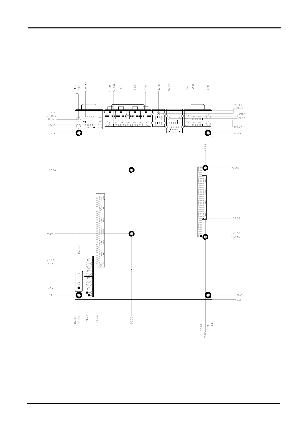
1.5 Board Layout
Chapter 1 Introduction
User’s Manual
3
Page 8
Chapter 2. Installation
Chapter 2 Installation
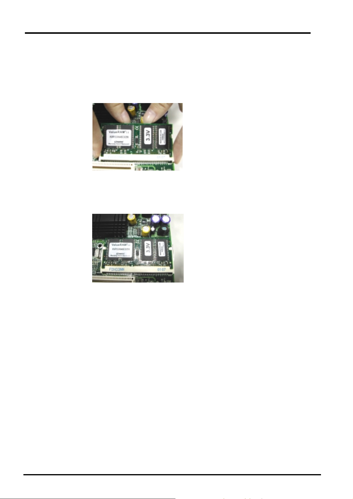
2.1 System Memory Installation
Step 1: Insert the RAM module into the SODIMM socket
Step 2: Press Module down till clip hold.
4
User’s Manual
Page 9
ATXC1
1
3
6
5
V
1
1
1
V
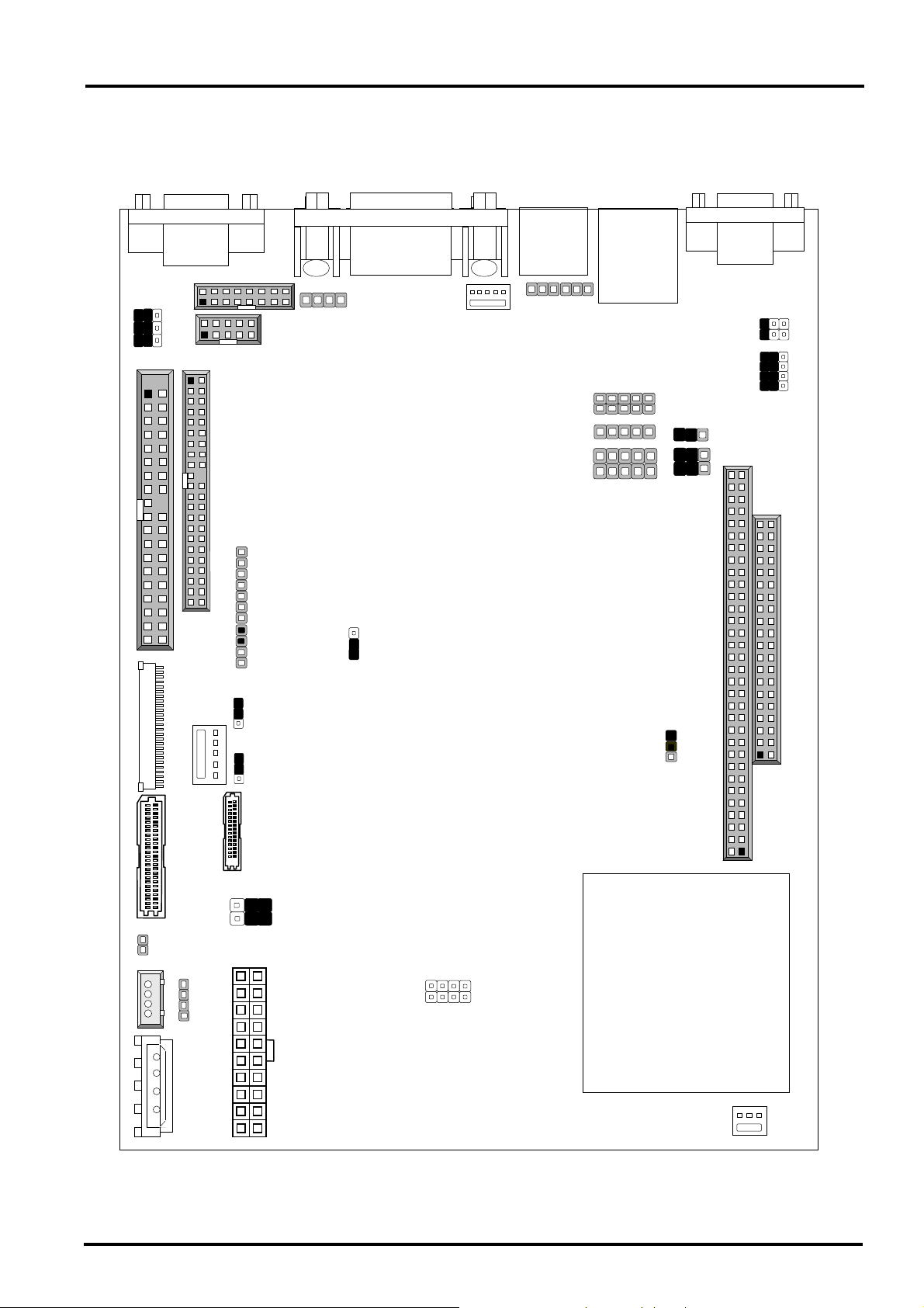
2.2 Jumper Settings and Connectors
2.2.1 Board Outline
SRIVB4
1
2
1
SRIVB3
IDEB1
1
49
1
PSW1
PS4W1
PS4M1
GACM1
1
1
26
FDCB1
1
2
LCD1
50
1
1
GAC1
COMB1
IDEA1
INVER1
1
1
1
29
2
SBVA1
12
1
JFA1
2
30
1
PLRS1
VLCD1
LVDSC1
LNO1 SPEAK1MIC1 LNI1
LPTB1
1
CDIN1
SCF1
6
5
PSA1
SLCDA1
1
ISPKR1
1
KM1
IKBM1
USBA1
IRDA1
2
1
2
1
USBLN1
DIOA1
CMOS1
10
1
10
9
1
SRIVB1
1
CPU1
Chapter 2 Installation
COMF1
SC2T1
2
1
9
1
SRIVB2
CONA1
FAN1
SC2T2
C
1
A
B
3
1
12
CONB1
1
D
User’s Manual
5
Page 10
Chapter 2. Installation
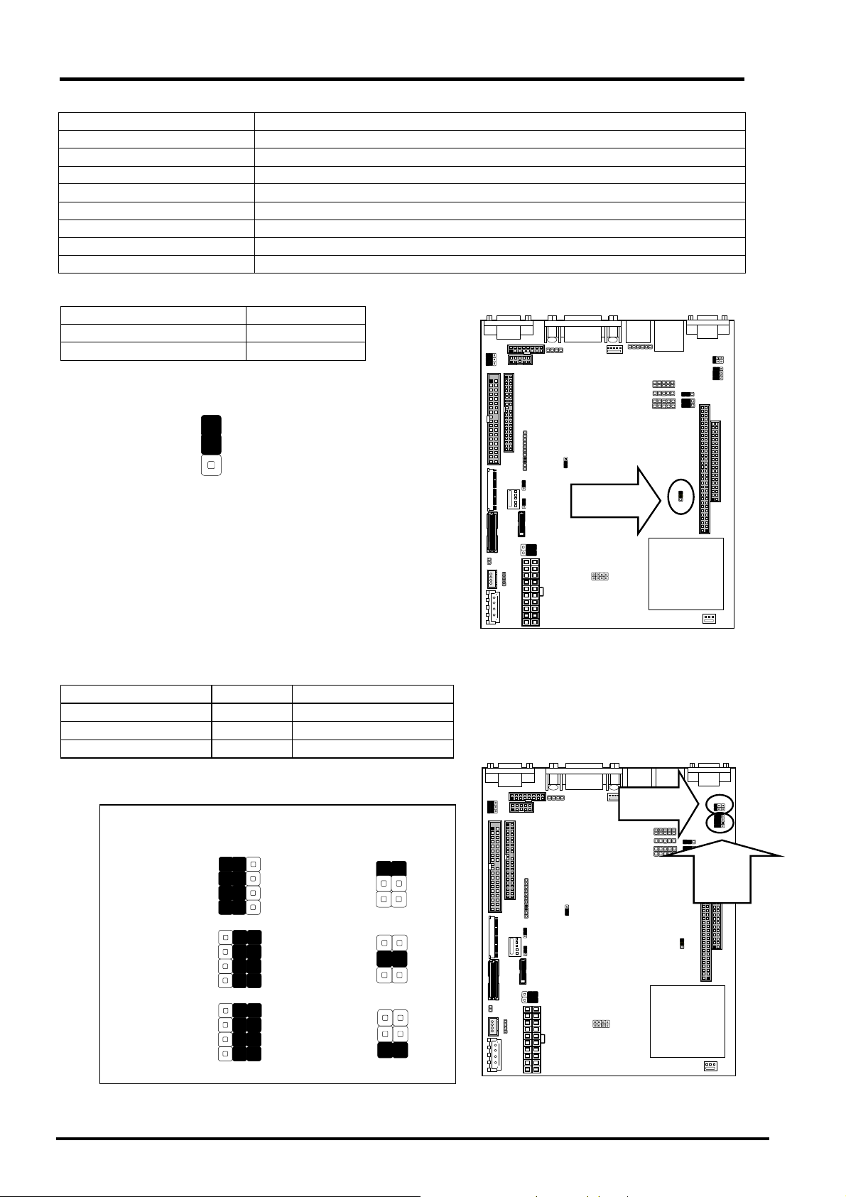
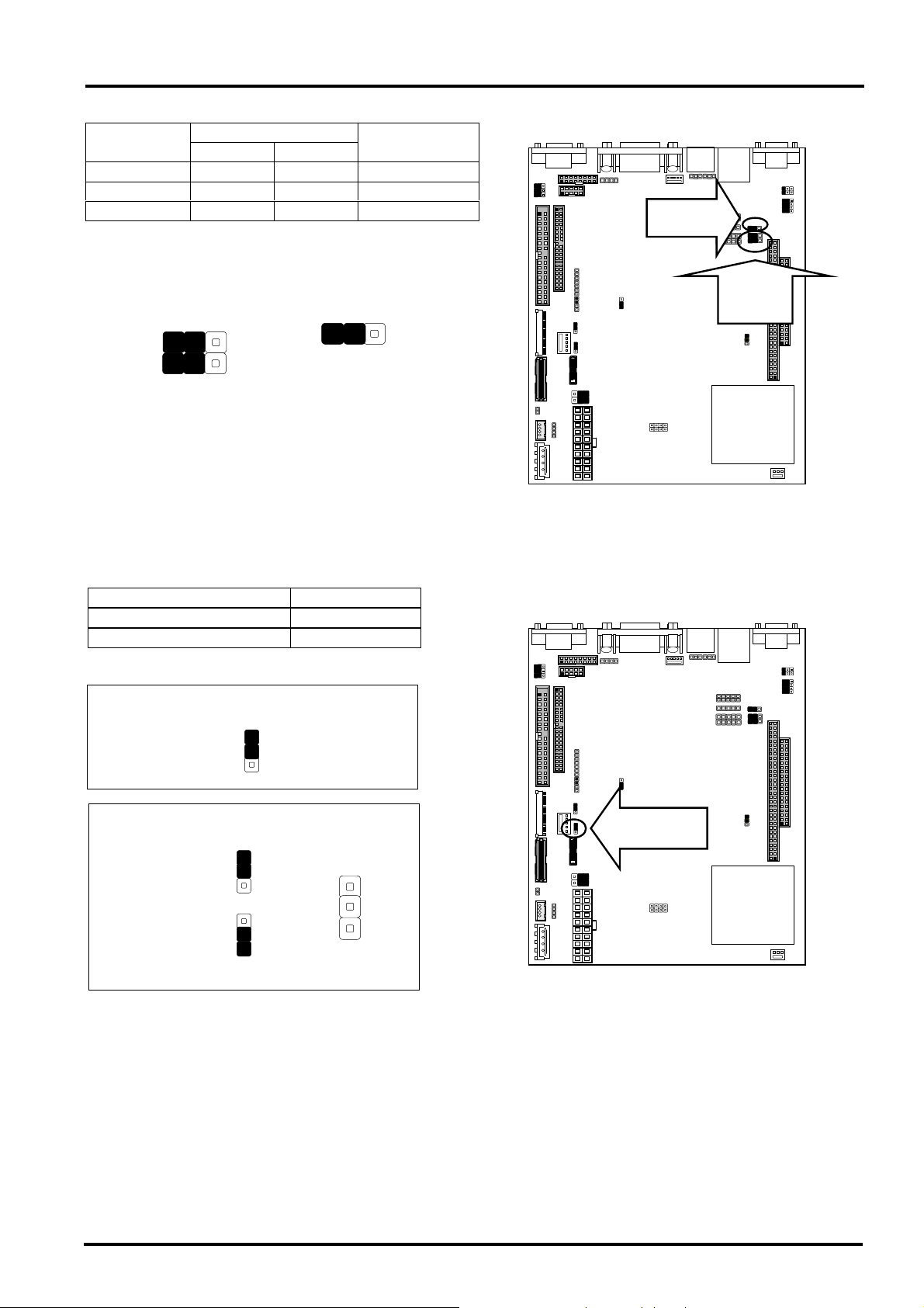
2.2.2 Jumper Settings Summary
LOCATION FUNCTION
CMOS1 Clear CMOS Data
SC2T1/SC2T2 Select COM1 Type
SRIVB1/SRIVB2 Select COM1, COM2 port pin 9 Type
VLCD1 Select Panel Voltage
SBVA1 Select AT/ATX Power
SCF1 Master/Slave Select
SRIVB3/SRIVB4 Select COM3, COM4 Pin9 Type
SLCDA1 Select Panel Type
!" CMOS1 : Clear CMOS Da ta
Description CMOS1
Normal (Default) 1-2
Clear CMOS 2-3
CMOS1
1
2
3
!"SC2T1/SC2T2: Select COM1 Type
COM1 TYPE SC2T1 SC2T2
RS-232 (Default) 1-2 1-5,2-6,3-7,4-8
RS-422 3-4 5-9,6-10,7-11,8-12
RS-485 5-6 5-9,6-10,7-11,8-12
SC2T2
SC2T1
RS-232
4
12
9 1
1
5
2
6
CMOS1
SC2T1
SC2T2
RS-422
RS-485
6
User’s Manual
Page 11
V
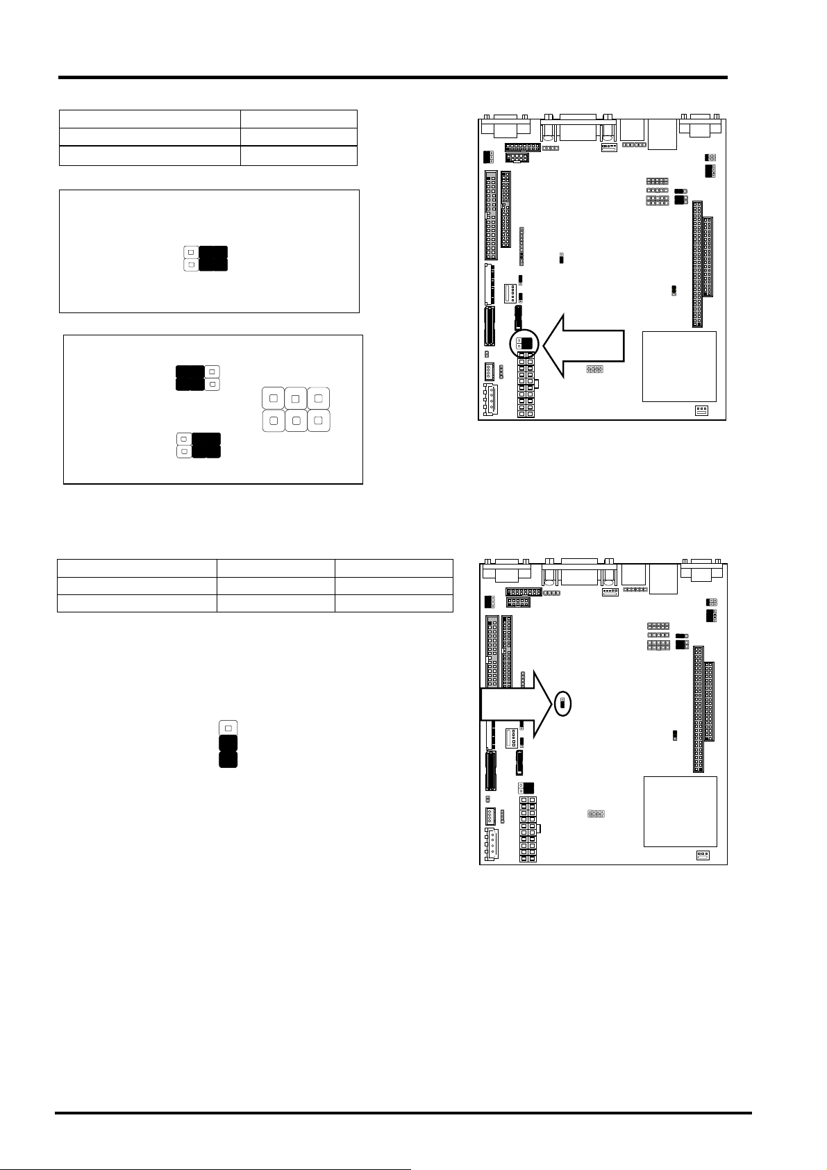
!"SRIVB1, SRIVB2: Select COM1, COM2 port pin 9 Type
Pin 9 Type
SRIVB1
COM1 COM2
SRIVB2
RI (Default) 1-3 2-4 1-2
+5V 3-5 4-6 1-2
+12V 3-5 4-6 2-3
Chapter 2 Installation
SRIVB2
SRIVB1
2 4 6
1 3 5
SRIVB2
1 2 3
!" VLCD1: Select Panel Voltage
Panel Voltage VLCD1
+3.3V (Default) 1-2
+5V 2-3
Default:
VLCD1
1
2
3
SRIVB1
3.3V (Default)
5V
User’s Manual
VLCD1
1
2
3
1
2
3
VLCD1
1
2
3
LCD1
7
Page 12
Chapter 2. Installation
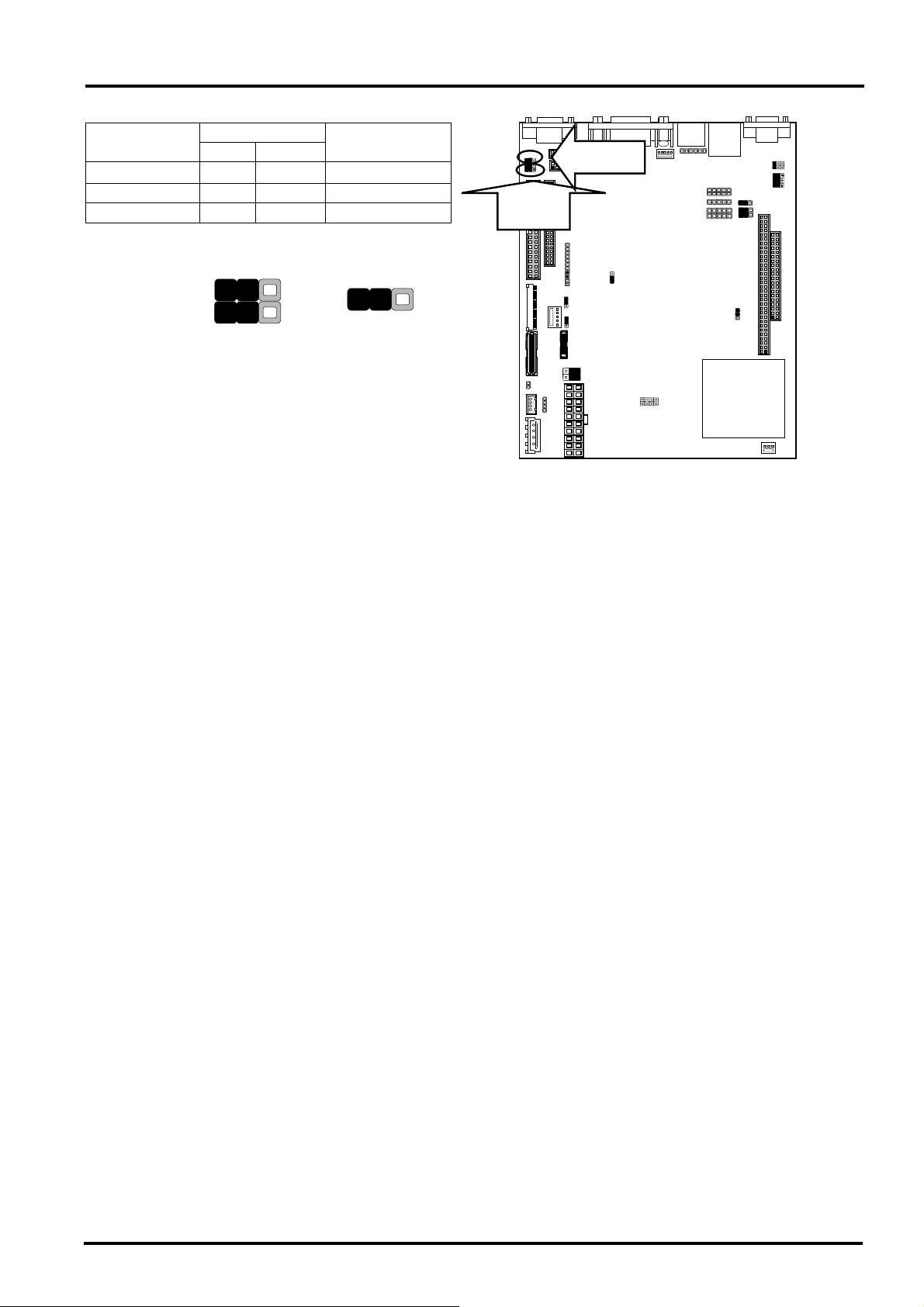
!"SBVA1: Select power supply Type
Power Type SBVA1
AT 1-3,2-4
ATX(Default)
3-5,4-6
Default:
SBVA1
2 4 6
1 3 5
(Default)
AT
ATX
2 4 6
2 4 6
1 3 5
2 4 6
1 3 5
1 3 5
!"SCF1: Master/Slave Select
Compact Flash Card ATA Disk Chip SCF1
Master Slave 1-2
Slave Master 2-3 (Default)
SCF1
1
3
SCF1
SBVA1
8
User’s Manual
Page 13
!"SRIVB3,4:Select COM3,COM4 Pin9 Type
PIN 9 Type
RI(Default)
SRIVB3
com3 com4
1-3 2-4
SRIVB4
1-2
+5V 3-5 4-6 1-2
+12V 3-5 4-6 2-3
2 4 6
1 2 3
1 3 5
SRIVB3
SRIVB4
SRIVB3
SRIVB4
Chapter 2 Installation
User’s Manual
9
Page 14
Chapter 2. Installation
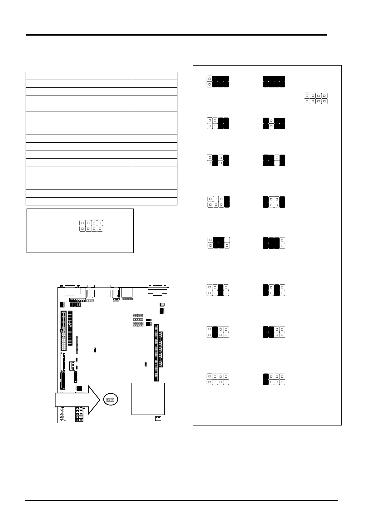
!"SLCDA1:Select Panel Type (2x4 Pin)
Note: Different type of LCD panel with the same resolution will have different jumper setting for
selection.
Panel Type SLCD1
640 x 480 TFT 1-2,3-4,5-6,7-8
800 x 600 TFT 3-4,5-6,7-8
1024 x 768 TFT 2pixel/Clk at 32MH Z 1-2,5-6,7-8
1280 x 1024 TFT 5-6,7-8
800 x 600 TFT
640X480 TFT
SLCD1A1
2 4 6 8
1 3 5 7
640 x 480 DSTN 1-2,3-4,7-8
800 x 600 DSTN 3-4,7-8
1024 x 768 DSTN 1-2,7-8
1024 x 768 TFT 1pixel/Clk at 65MHZ 7-8
1280 x 1024 TFT
1024 x 768 TFT 2pixel/Clk at 32MHZ
640 x 480 TFT 1-2,3-4,5-6
800 x 600 TFT 3-4,5-6
1024 x 768 TFT 1-2,5-6
1280 x 1024 TFT 5-6
1400 x 1050 TFT 2pixel/Clk at 54MHZ 1-2,3-4
800 x 600 DSTN
640 x 480 DSTN
800 x 600 DSTN 3-4
1024 x 768 DSTN 1-2
1280 x 1024 DSTN OFF
1024 x 768 DSTN
Default
All OFF:
2 4 6 8
1 3 5 7
SLCDA1
SLCDA1
1024x768 TFT/ pixel/ Clk at 65MHZ
800 x 600 TFT
640 x 480 TFT
1024 x 768 TFT 1280 x 1024 TFT
1400 x 1050 TFT 2pixel/Clk at 54MHZ 800 x 600 DSTN
1024x1024 DSTN 1280x1024 DSTN
10
User’s Manual
Page 15

Chapter 2 Installation
2.2.3 I/O Connectors Summary
LOCATION FUNCTION
PLRS1 Power LED, HD, LED, Reset, Speaker Connector
IRDA1 IRDA Connector
USBA1
USB Port #3 Connecto r 2!5 Pin 2.54mm
LPTB1 Parallel Port Connector
LVDSC1
LVDS Panel Con nector 2!15P 1.0mm SMT
FDCB1 Slim Floppy Interface Connector
INVER1 LCD INVERTER Connector
LCD1 Panel LCD Connector
IDEA1 IDE Interface Connector (44 Pin 2.0mm Pitch Header)
IDEB1 IDE Interface Connector (40 Pin 2.54mm Pitch Header)
PS4W1 4-Pin Power Connector (WAFER 4P 2.00mm)
PSA1 20 Pin ATX Power Connector
DIOA1
Digital Input/ Digital Output Ports (2!5 Pin 2.54mm Header)
ATXC1 For ATX Function
PSW1 For ATX Power Button
CONA1 /CONB1 PC/104 Connector (8 bit/16 bit)
FAN1 3Pin FAN Connector
COMF1 Serial port #1 & #2 Connector, Double stack 9 Pin D-USB MALE
USBLN1 LAN & USB port #1 & #2 Connector Double stack 8 Pin RJ45+8 P in USB
VGACM1 VGA & Serial port #3, Double stack 15 Pin D-SUB Female & 9 Pin D-SUB Male
PS4M1 4Pin Power Connector (Big-4P Male)
CF1 Compact Flash Connector
IKBM1 Internal Keyboard, Mouse Connector (6Pin 2.54mm Head er)
KM1 Keyboard & Mouse Connector, Double stack 6 Pin mini DIN Female
VGAC1
Internal VGA Connector (2!8 Pin 2.54mm Pitch Header)
MIC1 MIC IN 5Pin-PHONE Jack
LNI1 Line IN 5Pin-PHONE Jack
CDIN1 CD_IN Connector
ISPKR1 Internal Speaker Connector
LNO1 Line out 5Pin-PHONE Jack
SPEAK1 Header phone connector 5Pin-PHONE Jack
COMB1 Serial Port #4 Connector (Header)
User’s Manual
11
Page 16
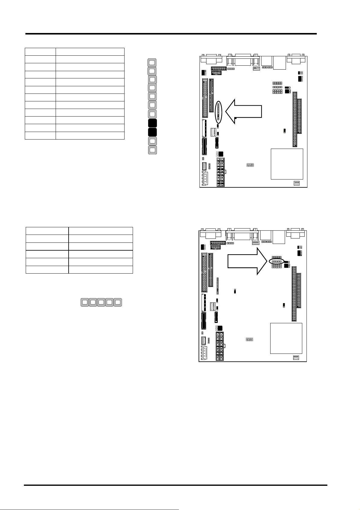
Chapter 2. Installation
!"PLRS1: Power LED, HD LED, Reset, Speaker Connector (11 Pin 2.54mm)
Pin No. Description
1 Power LED +
2 Power LED +
3 GND
4 HDD LED +
5 HDD LED 6 RESET SW +
7 RESET SW – (GND)
8 External Speaker -
9 Internal Buzzer 10 NC
11 External Speaker +
Default :
8-9 (ON) Internal Buzzer
1
11
PLRS1
PLRS1
!"IRDA1: IRDA Connector
Pin No. Description
1 +3.3V
2 NC
3 IRRX
4 GND
5 IRTX
1
IRDA1
5
IRDA1
12
User’s Manual
Page 17
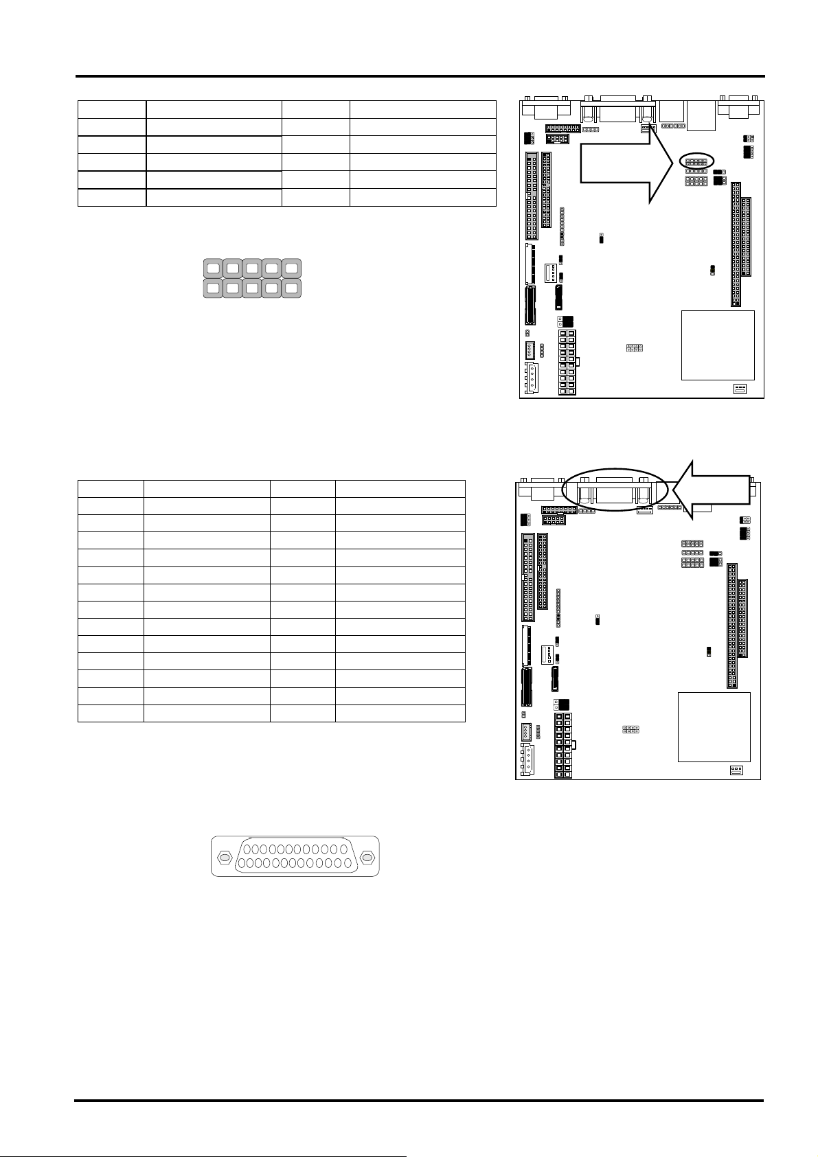
"
"USBA1: USB Port #3 & #4 Connector 2x5 Pin 2.54mm
""
Pin No. Description Pin No. Description
1 +5VSB 2 +5VSB
3 USBD2- 4 USBD35 USBD2+ 6 USBD3+
7 Ground 8 Ground
9 USB Port #3Ground 10 USB Port #4Ground
9
1
10
USBA1
2
Chapter 2 Installation
USBA1
"
"LPTB1: Parallel Port Connector (25 Pin D-Sub)
""
Pin No. Description Pin No. Description
1 Strobe # 14 Auto Form Feed #
2 Data0 15 Error #
3 Data1 16 Initialize #
4 Data2 17 Printer Select IN #
5 Data3 18 Ground
6 Data4 19 Ground
7 Data5 20 Ground
8 Data6 21 Ground
9 Data7 22 Ground
10 Acknowledge # 23 Ground
11 Busy 24 Ground
12 Paper Empty 25 Ground
13 Printer Select
14
LPTB1
25
1
13
LPTB1
User’s Manual
13
Page 18
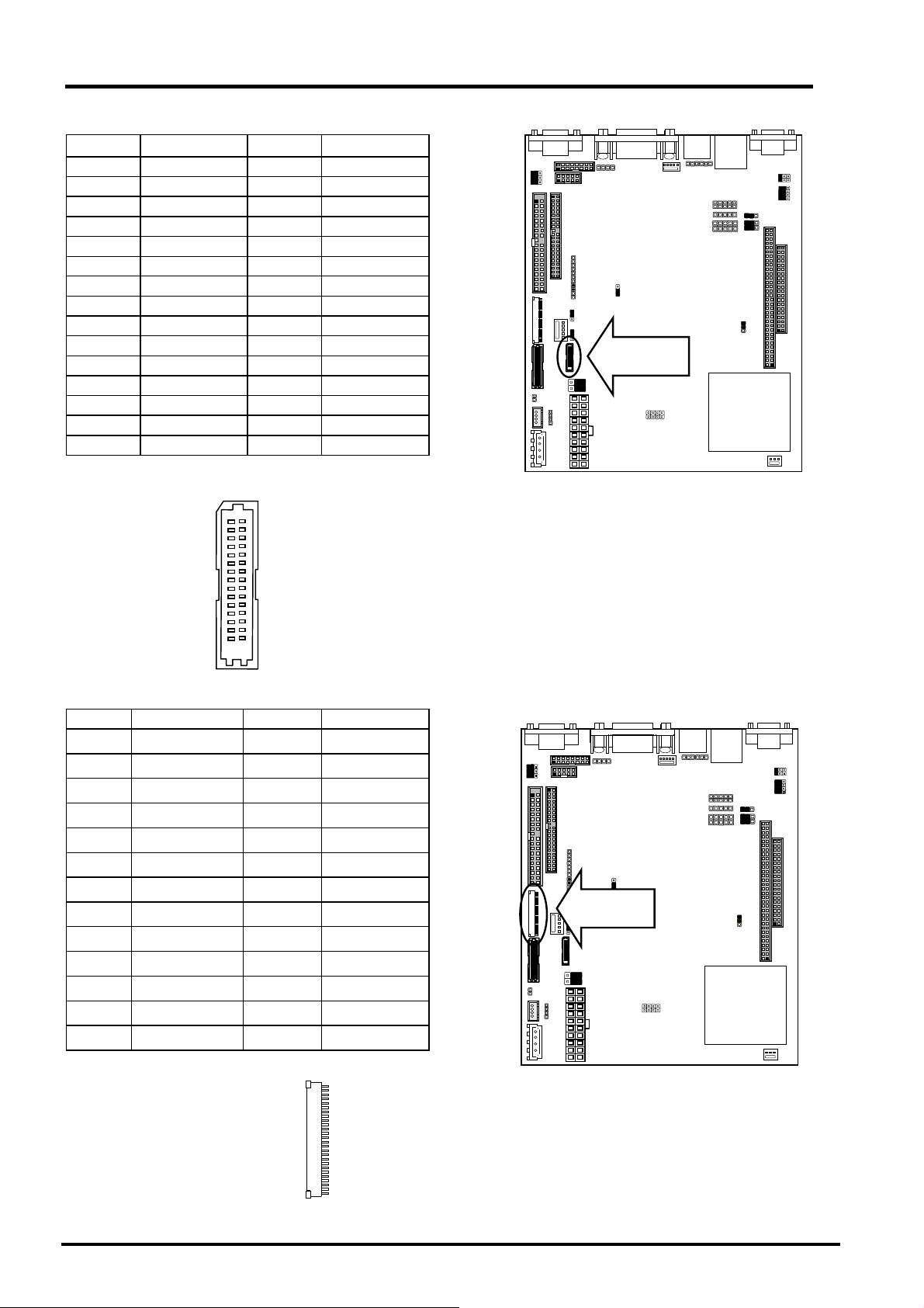
Chapter 2. Installation
"
"LVDSC1
""
Pin No.
LVDS Panel Connector 2x15P 1.0mm SMT
:
:
:
:
Description Pin No. Description
1 FVCC 2 FVCC
3 GND 4 GND
5 NC 6 +12V
7 Y0M 8 Z0M
9 Y0P 10 Z0P
11 GND 12 GND
13 Y1M 14 Z1M
15 Y1P 16 Z1P
17 GND 18 GND
19 Y2M 20 Z2M
21 Y2P 22 Z2P
23 GND 24 GND
25 YCM 26 ZCM
27 YCP 28 ZCP
29 GND 30 GND
1 2
LVDSC1
LVDSC1
29
30
"
"FDCB1: Slim Floppy Interface Connector (26 Pin Header)
""
Pin No. Description Pin No. Description
1 VCC 14 STEP2 INDEX- 15 GND
3 VCC 16 WD4 DSA- 17 GND
5 VCC 18 WE6 DSKCHG- 19 GND
7 NC 20 TRAK08 NC 21 GND
9 NC 22 WP-
10 MOA- 23 GND
11 NC 24 RDATA12 DIR- 25 GND
13 NC 26 HEAD-
FDCB1
14
26
FDCB1
1
User’s Manual
Page 19
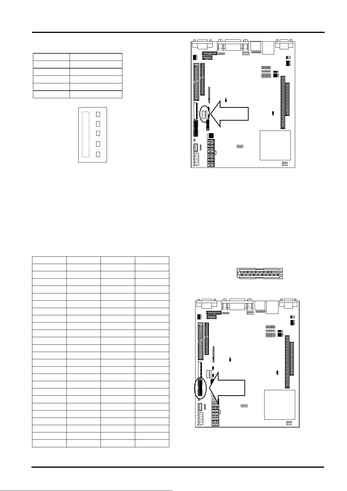
"
"INVER1: LCD INVERTER Connector
""
Pin No. Description
1 GND
2 +5V
3 +12V
4 ENAVEE
5 Bright
Chapter 2 Installation
INVER1
1
2
3
4
5
INVER1
#Regular pin 5 (bright) output is 1.8V.
But output can be adjusted by below software tools.
EM60SAWD.EXE for output: 0 ~ 1.8V
EM60LAWD.EXE for output: 0 ~ 3.3V
Brightness Adjust Operation:
Power-on by DOS booting disk, execute software tool and push "+" bottom to increase voltage or push "-"
bottom to decrease voltage.
"
"LCD1: Panel LCD Connector (50Pin 1.0mm JST Header)
""
Pin No. Signal Pin No. Signal
1 FVCC 2 FVCC
2
50
3 LP 4 FLM
5 M/DE 6 NC
7 ENAVEE 8 ENAVDD
1
LCD1
49
9 SHFCLK 10 +12V
11 GND 12 GND
13 P0 14 P1
15 P2 16 P3
17 P4 18 P5
19 P6 20 P7
21 P8 22 P9
23 P10 24 P11
25 P12 26 P13
27 P14 28 P15
29 GND 30 P16
31 P17 32 P18
33 P19 34 P20
35 P21 36 P22
37 P23 38 GND
39 P24 40 P25
41 P26 42 P27
LCD1
43 P28 44 P29
45 P30 46 P31
47 P32 48 P33
49 P34 50 P35
User’s Manual
15
Page 20

Chapter 2. Installation
!"Flat Panel Interface Pins listing for DSTN and color TFT LCD
SR7D[3] 0 0 0 0 0 0
SR70[0] 1 1 1 0 0 0
SR79[1-0] 10 10 10 10 10 10
SR7D[2-0] 001 000 010 010 000 010
Pin Name STN8 STN16 ATN24 DSTN8 DSTN16 DSTN24
FPD0 R0 R0 R0 LR0 LR0 LR0
FPD1 G0 G0 G0 LR3
FPD2 B0 B0 B0 LG0 LG0 LG0
FPD3 R1 R1 R1
FPD4 G1 G1 G1 LB0 LB0 LB0
FPD5 B1 B1 B1
FPD6 R2 R2 R2 LR1 LR1 LR1
FPD7 G2 G2 G2 LG3
FPD8 B2 B2 LG1 LG1
FPD9 R3 R3
FPD10 G3 G3 LB1 LB1
FPD11 B3 B3
FPD12 R4 R4 LR2 LR2
FPD13 G4 G4 LB3
FPD14 B4 B4 LG2 LG2
FPD15 R5 R5
FPD16 G5 LB2
FPD17 B5
FPD18 R6 UR0 UR0 UR0
FPD19 G6 UR3
FPD20 B6 UG0 UG0 UG0
FPD21 R7
FPD22 G7 UB0 UB0 UB0
FPD23 B7
FPD24 UR1 UR1 UR1
FPD25 UG3
FPD26 UG1 UG1
FPD27
FPD28 UB1 UB1
FPD29 UB3
FPD30 UR2 UR2
FPD31 UB3
FPD32 UG2 UG2
FPD33
FPD34 UB2
FPD35
16
User’s Manual
Page 21

Chapter 2 Installation
SR7D[3] 0 0 0 0 0 0 0 0 0
SR70[0] 1 1 1 1 1 1 1 1 1
SR79[1-0] 00 00 00 00 00 00 00 00 00
SR7D[2-0] 000 010 000 010 000 010 000 010 001
Pin Name TFT9
TFT2!!!!9
TFT12
TFT2!!!!12
TFT15
TFT2!!!!15
TFT18
TFT2!!!!18
TFT24
FPD0 R0 R00 R2
FPD1 R10 R0
FPD2 R0 R00 R1 R01 R3
FPD3 R10 R11
FPD4 R0 R00 R1 R01 R2 R02 R4
FPD5 R10 R11 R12
FPD6 R0 R00 R1 R01 R2 R02 R3 R03 R5
FPD7 R10 R11 R12 R13 R1
FPD8 R1 R01 R2 R02 R3 R03 R4 R04 R6
FPD9 R11 R12 R13 R14
FPD10 R2 R02 R3 R03 R4 R04 R5 R05 R7
FPD11 R12 R13 R14 R15
FPD12 G0 G00 G2
FPD13 G10 G0
FPD14 G0 G00 G1 G01 G3
FPD15 G10 G11
FPD16 G0 G00 G1 G01 G2 G02 G4
FPD17 G10 G11 G12
FPD18 G0 G00 G1 G01 G2 G02 G3 G03 G5
FPD19 G10 G11 G12 G13 G1
FPD20 G1 G01 G2 G02 G3 G03 G4 G04 G6
FPD21 G11 G12 G13 G14
FPD22 G2 G02 G3 G03 G4 G04 G5 G05 G7
FPD23 G12 G13 G14 G15
FPD24 B0 B00 B2
FPD25 B10 B0
FPD26 B0 B00 B1 B01 B3
FPD27 B10 B11
FPD28 B0 B00 B1 B01 B2 B02 B4
FPD29 B10 B11 B12
FPD30 B0 B00 B1 B01 B2 B02 B3 B03 B5
FPD31 B10 B11 B12 B13 B1
FPD32 B1 B01 B2 B02 B3 B03 B4 B04 B6
FPD33 B11 B12 B13 B14
FPD34 B2 B02 B3 B03 B4 B04 B5 B05 B7
FPD35 B12 B13 B14 B15
User’s Manual
17
Page 22
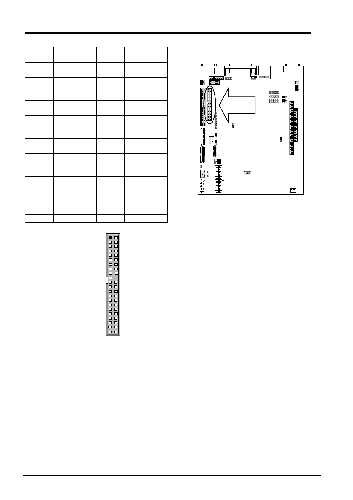
Chapter 2. Installation
"IDEA1: IDE Interface Connector (44Pin 2.0mm Pitch Header)
Pin No. Description Pin No. Description
1 Reset # 2 Ground
3 Data 7 4 Data 8
5 Data 6 6 Data 9
7 Data 5 8 Data 10
9 Data 4 10 Data 11
11 Data 3 12 Data 12
13 Data 2 14 Data 13
15 Data 1 16 Data 14
17 Data 0 18 Data 15
19 Ground 20 Key
21 DMA REQ # 22 Ground
23 IOW # 24 Ground
25 IOR # 26 Ground
27 IOCHRDY 28 Ground
29 DMA ACK # 30 Ground
31 Interrupt 32 NC
33 SA 1 34 NC
35 SA 0 36 SA 2
37 HDC CS 0# 38 HDC CS 1#
39 HDD Active 40 Ground
41 VCC 42 VCC
43 Ground 44 NC
1
2
IDEA1
43
44
IDEA1
18
User’s Manual
Page 23
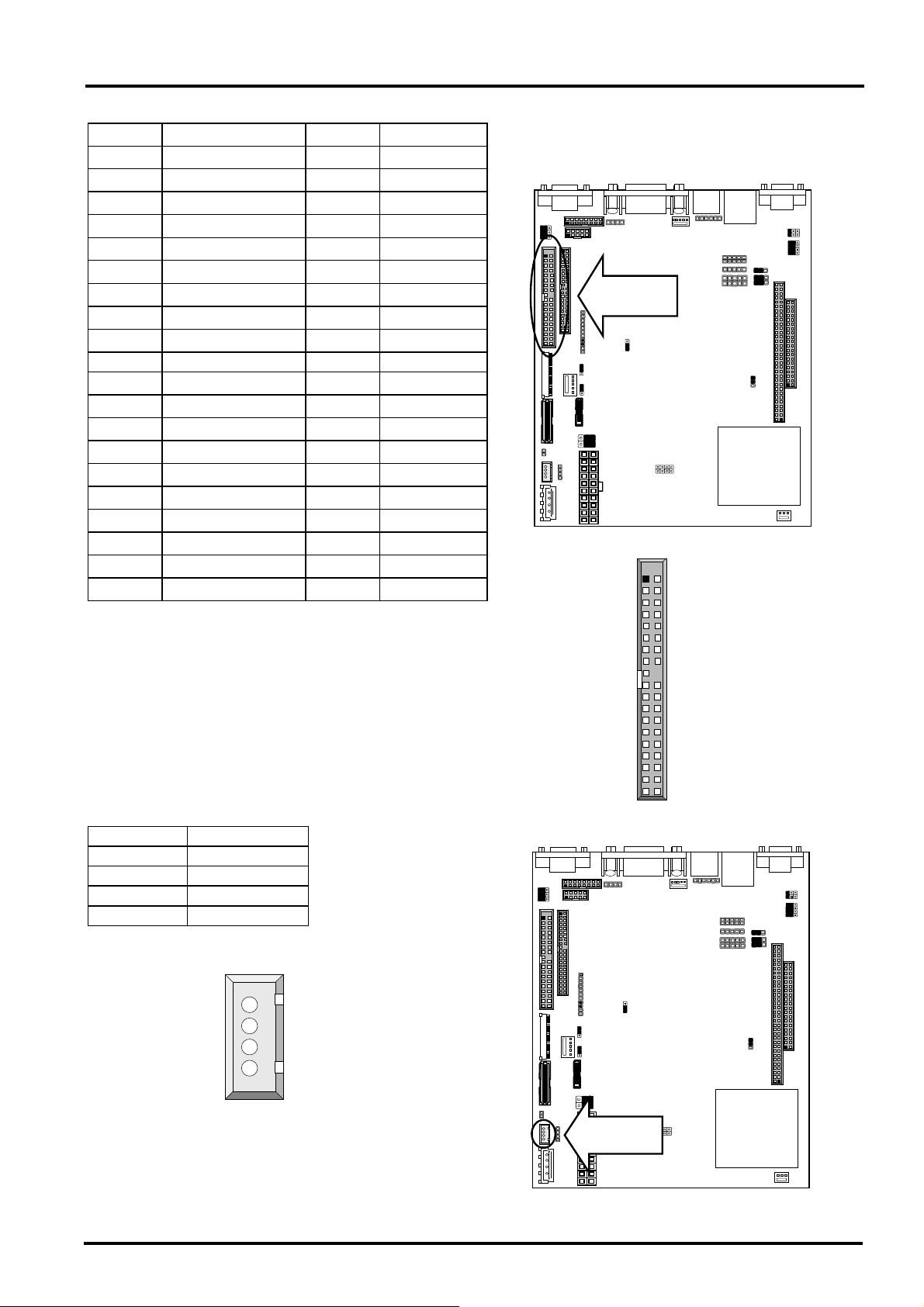
"
"IDEB1: IDE Interface Connector (40Pin 2.54mm Pitch Header)
""
Pin No. Description Pin No. Description
1 Reset # 2 Ground
3 Data 7 4
5 Data 6 6 Data 9
Data 8
7 Data 5 8 Data 10
9 Data 4 10 Data 11
11 Data 3 12 Data 12
13 Data 2 14 Data 13
15 Data 1 16 Data 14
17 Data 0 18 Data 15
19 Ground 20 Key
21 DMA REQ# 22 Ground
23 IOW # 24 Ground
25 IOR # 26 Ground
27 IOCHRDY 28 Ground
29 DMA ACK # 30 Ground
31 Interrupt 32 NC
33 SA1 34 PD80P
35 SA0 36 SA2
37 HDC CS0 # 38
HDC CS1 #
39 HDD Active LED # 40 Ground
IDEB1
"
"PS4W1: 4-Pin Power Connector (WAFER 4P 2.00mm)
""
Pin No. Description
1 GND
2 -5V
3 GND
4 -12V
1
4
PS4W1
IDEB1
1
39
PS4W1
Chapter 2 Installation
2
User’s Manual
19
Page 24
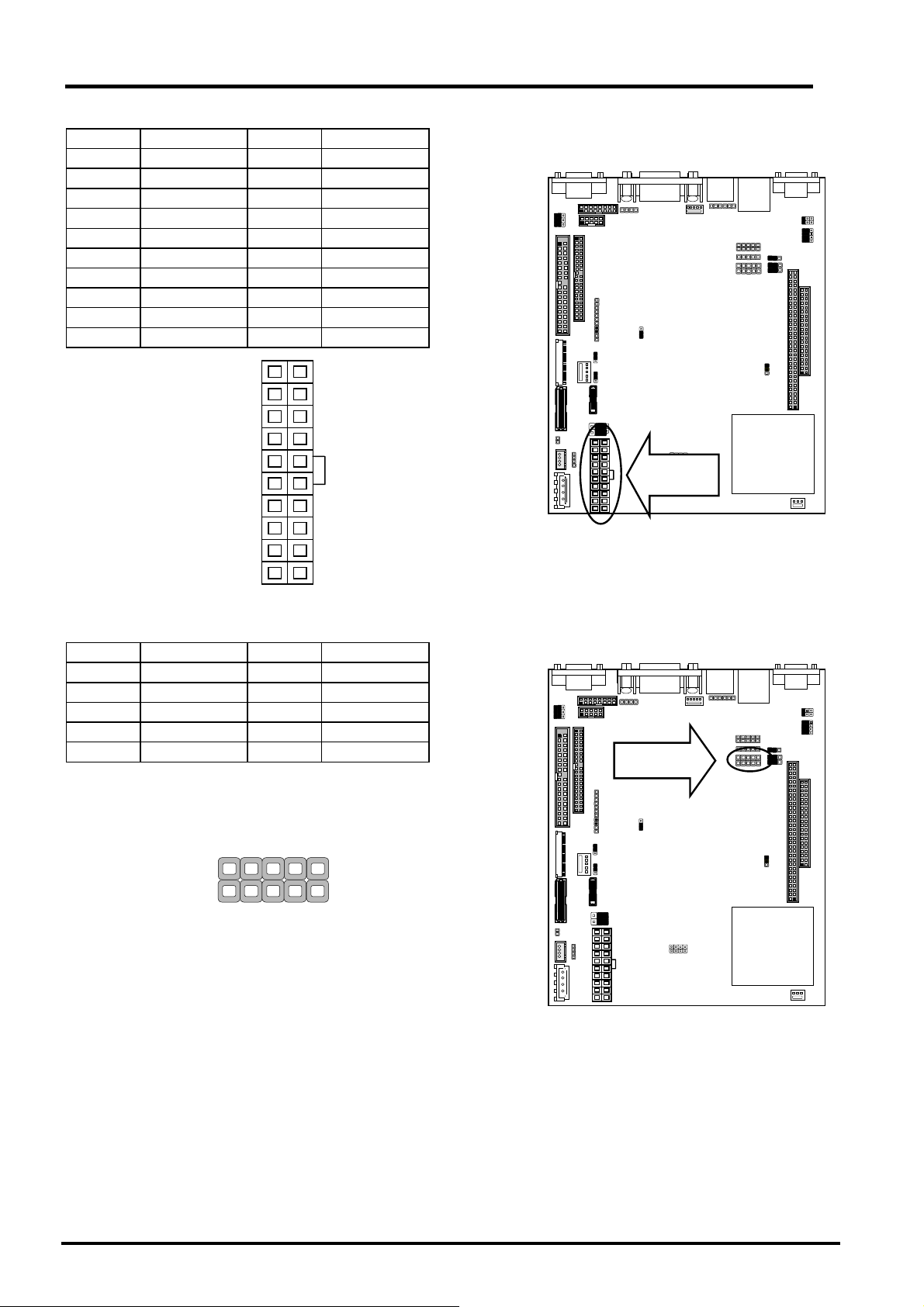
Chapter 2. Installation
""""PSA1: 20 Pin ATX Power Connector
Pin No. Description Pin No. Description
1 +3.3V 11 +3.3V
2 +3.3V 12 -12V
3 GND 13 GND
4 +5V 14 PS-ON
5 GND 15 GND
6 +5V 16 GND
7 GND 17 GND
8 Power Good 18 -5V
9 Stand-By 5V 19 +5V
10 +12V 20 +5V
10
20
"
"DIOA1: Digital Input/ Digital Output Ports(2x5 Pin 2.54mm Header)
""
Pin No. Description Pin No. Description
1 IN0 2 OUT0
3 IN1 4 OUT1
5 IN2 6 OUT2
7 IN3 8 OUT3
9 Ground 10 Ground
PSA1
2
1
1
11
10
DIOA1
9
PSA1
DIOA1
20
User’s Manual
Page 25
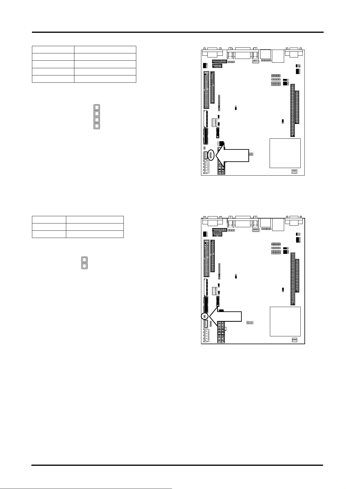
A
"
"ATXC1: For ATX Function
""
Pin No. Description
1 GND
2 +5V STANDBY
3 GND
4 PSON
ATXC1
1
4
"
"PSW1: For ATX Power Button
""
Pin No. Description
1 PANSW
2 GND
1
2
PSW1
TXC1
PSW1
Chapter 2 Installation
User’s Manual
21
Page 26
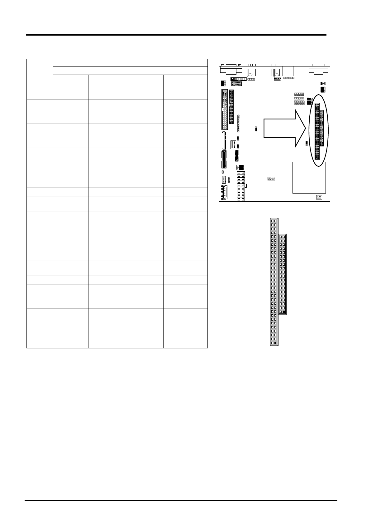
Chapter 2. Installation
"
" CONA1:PC/104 Connector
""
"
" CONB1:PC/104 Connector
""
8 bit
︵
︵
︵
︵
16 bit
︵
︵
︵
︵
︶
︶
︶
︶
︶
︶
︶
︶
Description
Pin No.
CONA1 CONB1
Row A Row B
Row C
Ground
Row D
Ground
1 IOCHCK# Ground SBHE# MEMCS16#
2 SD7 RSTDRV LA23 IOCS16#
3 SD6 +5V LA22 IRQ10
4 SD5 IRQ9 LA21 IRQ11
5 SD4 -5V LA20 IRQ12
6 SD3 DRQ2 LA19 IRQ15
7 SD2 -12V LA18 IRQ14
8 SD1 0 WS# LA17 DACK0#
9 SD0 +12V MEMR# DRQ0
10 IOCHRDY NC MEMW# DACK5#
11 AEN SMEMW# SD8 DRQ5
12 SA19 SMEMR# SD9 DACK6#
13 SA18 IOW# SD10 DRQ6
14 SA17 IOR# SD11 DACK7#
15 SA16 DACK3# SD12 DRQ7
16 SA15 DRQ3 SD13 +5V
17 SA14 DACK1# SD14 MASTER#
18 SA13 DRQ1 SD15 Ground
19 SA12 REFRESH# NC Ground
20 SA11 SYSCLK --- --21 SA10 IRQ7 --- --22 SA9 IRQ6 --- --23 SA8 IRQ5 --- --24 SA7 IRQ4 --- --25 SA6 IRQ3 --- --26 SA5 DACK2# --- --27 SA4 TC --- --28 SA3 BALE --- --29 SA2 +5V --- --30 SA1 OSC --- --31 SA0 Ground --- --32 Ground Ground --- ---
32
CONA1
1
CONA1/
CONB1
20
CONB1
1
C D
B A
22
User’s Manual
Page 27
"
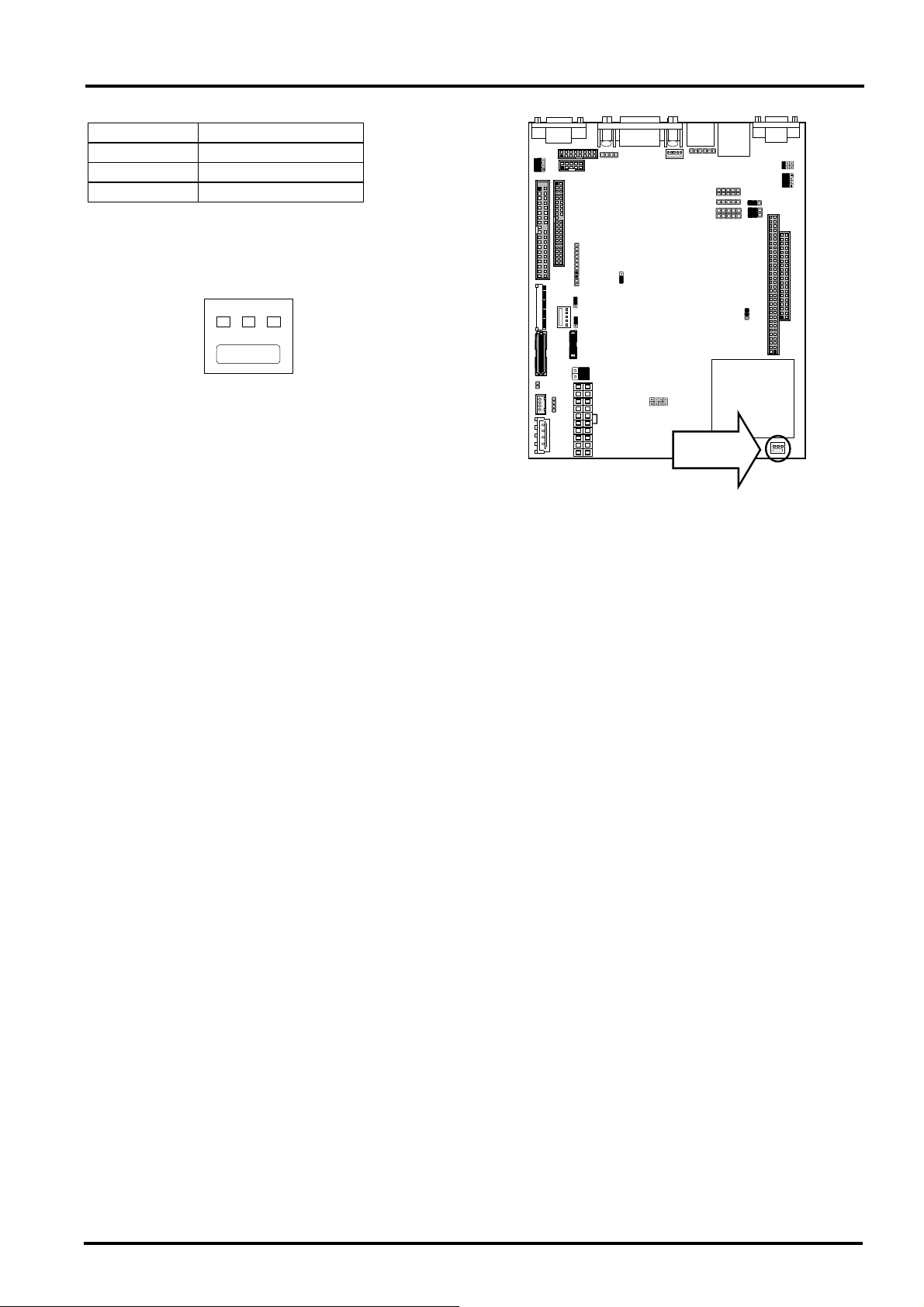
"FAN1: 3-Pin FAN Connector (For EM-660B only)
""
Pin No. Description
1 Ground
2 +5V
3 FAN Status
1 2 3
FAN1
Chapter 2 Installation
FAN1
User’s Manual
23
Page 28
Chapter 2. Installation
"
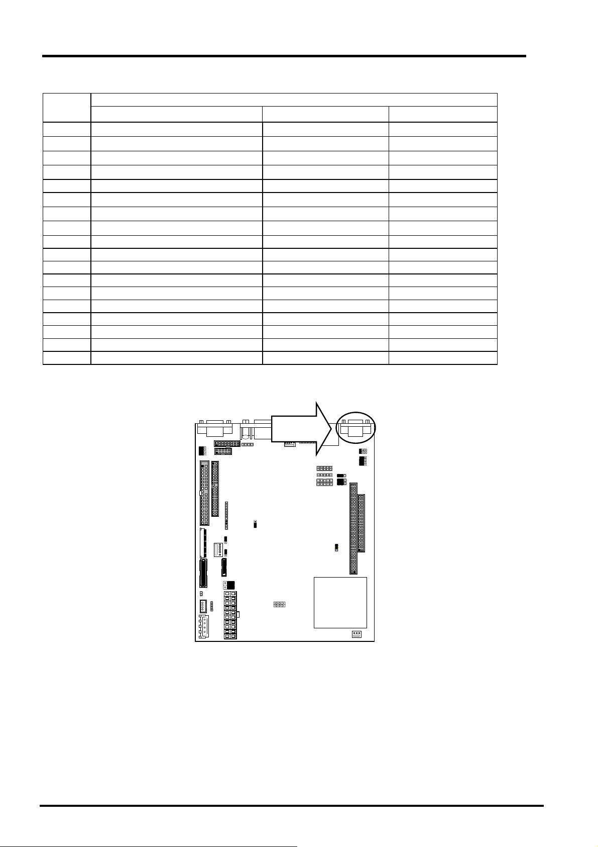
"COMF1
""
Double stack 9 Pin D-SUB MALE (Up: COM2; Down: COM1)
Pin No.
1
2
3
4
5 Ground NC NC
6
7
8
9 Type Select1 NC NC
10 DCD2#
11 RXD2
12 TXD2
13 DTR2#
14 GND
15 DSR2#
16 RTS2#
17 CTS2#
18 Type Select2
Serial port#1 Connector
:
:
:
:
Description
RS-232 RS-422 RS-485
Data Carrier Detect(DCD1)# Transmit Data-(TXD-)
Receive Data(RXD1) Transmit Data+(TXD+)
Trans mit Da ta(TXD1) Receive Data+(RXD+)
Data Terminal Ready(DTR1#) Receive Data-(RXD-)
Data set Ready(DSR1#)
Request To Send(RTS1#)
Clear To Send(CTS1#)
NC NC
NC NC
NC NC
Data-
Data+
NC
NC
COMF1
24
User’s Manual
Page 29
V
"
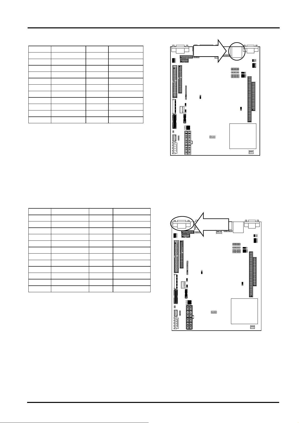
"USBLN1: LAN&USB port#1 Connector
""
Double stack 8 Pin USB+8 Pin RJ45
Pin No. Description Pin No. Description
1 ATX+ 2 ATX3 ARX+ 4 T45
5 T45 6 ARX7 T78 8 T78
9 -LALINK 10 +LALINK
11 -LAACT 12 +LAACT
13 LGND 14 LGND
15 USB0 VCC 16 USB DT017 USBDT0+ 18 USB-GND
19 USB1 VCC 20 USBDT121 USBDT1+ 22 USB-GND
"
"VGACM1: VGA & Serial port#3
""
Double stack 15 Pin D-SUB Female & 9 Pin D-SUB Male
Pin No. Description Pin No. Description
1 R 2 G
3 B 4 NC
5 VGAGND 6 VGAGND
7 VGAGND 8 VGAGND
9 NC 10 VGAGND
11 NC 12 D2DATA
13 HSYNC 14 VSYNC
15 D2CLK 16 NDCD3
17 NSIN3 18 NSOUT3
19 NDTR3 20 C3GND
21 NDSR3 22 NRTS3
23 NCTS3 24 Type Select3
Chapter 2 Installation
USBLN1
GACM1
User’s Manual
25
Page 30
Chapter 2. Installation
"
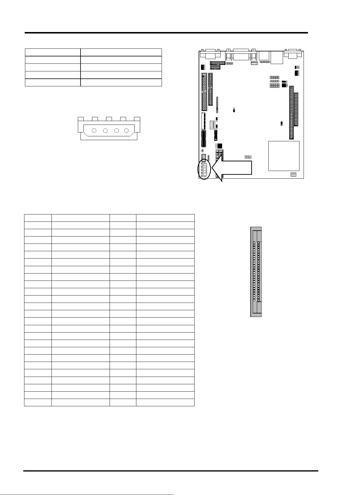
"PS4M1: 4 Pin Power Connector (Big-4P Male)
""
Pin No. Description
1 +12V
2 Ground
3 Ground
4 +5V
PS4M1
1 4
3 2
"
"CF1: Compact Flash Connector (on solder side)
""
Pin No. Description Pin No. Description
1 GND 26 CD12 DATA3 27 DATA11
3 DATA4 28 DATA12
4 DATA5 29 DATA13
5 DATA6 30 DATA14
6 DATA7 31 DATA15
7 CE1# 32 CE2#
8 GND 33 VS1#
9 OE# 34 IOR#
10 GND 35 IOW#
11 GND 36 WE#
12 GND 37 NC
13 CFVCC3 38 CFVCC3
14 GND 39 CSEL
15 GND 40 VS2#
16 GND 41 RESET
17 GND 42 IOCARDY
18 A2 43 NC
19 A1 44 REG#
20 A0 45 DASP#
21 DATA0 46 DIAG#
22 DATA1 47 DATA8
23 DATA2 48 DATA9
24 WP 49 DATA10
25 CD2- 50 GND
PS4M1
CF1
26
50
$ CF1 is on the solder side
1
25
26
User’s Manual
Page 31
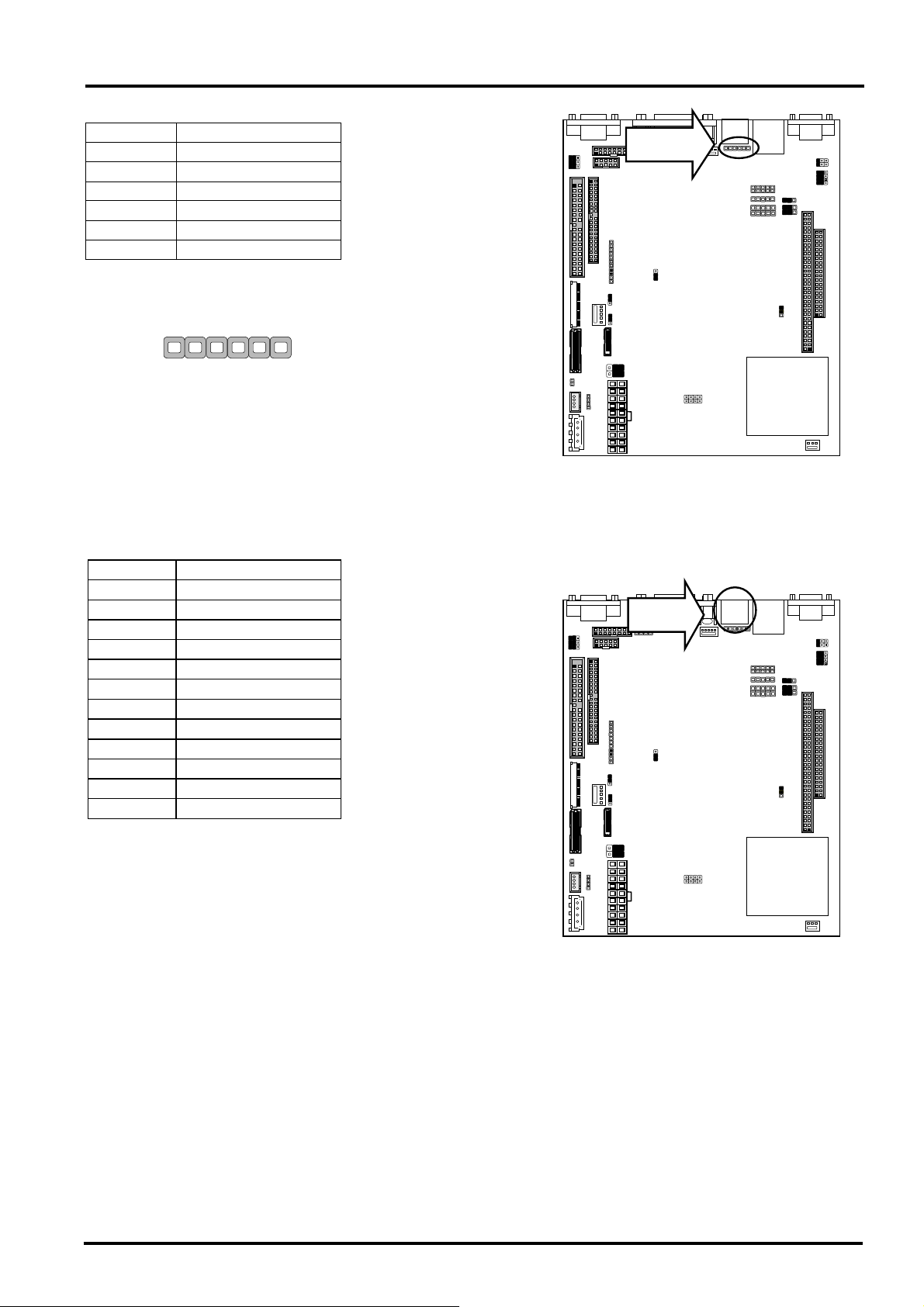
!"IKBM1: Internal Keyboard, Mouse Connecter
Pin No. Description
1 PS/2 Keyboard Data
IKBM1
2 PS/2 Mouse Data
3 Ground
4 +5V
5 PS/2 Keyboard Clock
6 PS/2 Mouse Clock
1
6
IKBM1
!"KM1: Keyboard & Mouse Connector, Double stack 6 Pin mini DIN Female
Pin No. Description
1 KBDATA
2 NC
KM1
3 GND
4 +5V
5 KBCLK
6 NC
7 MSDATA
8 NC
9 GND
10 +5V
11 MSCLK
12 NC
Chapter 2 Installation
User’s Manual
27
Page 32
Chapter 2. Installation
V
V
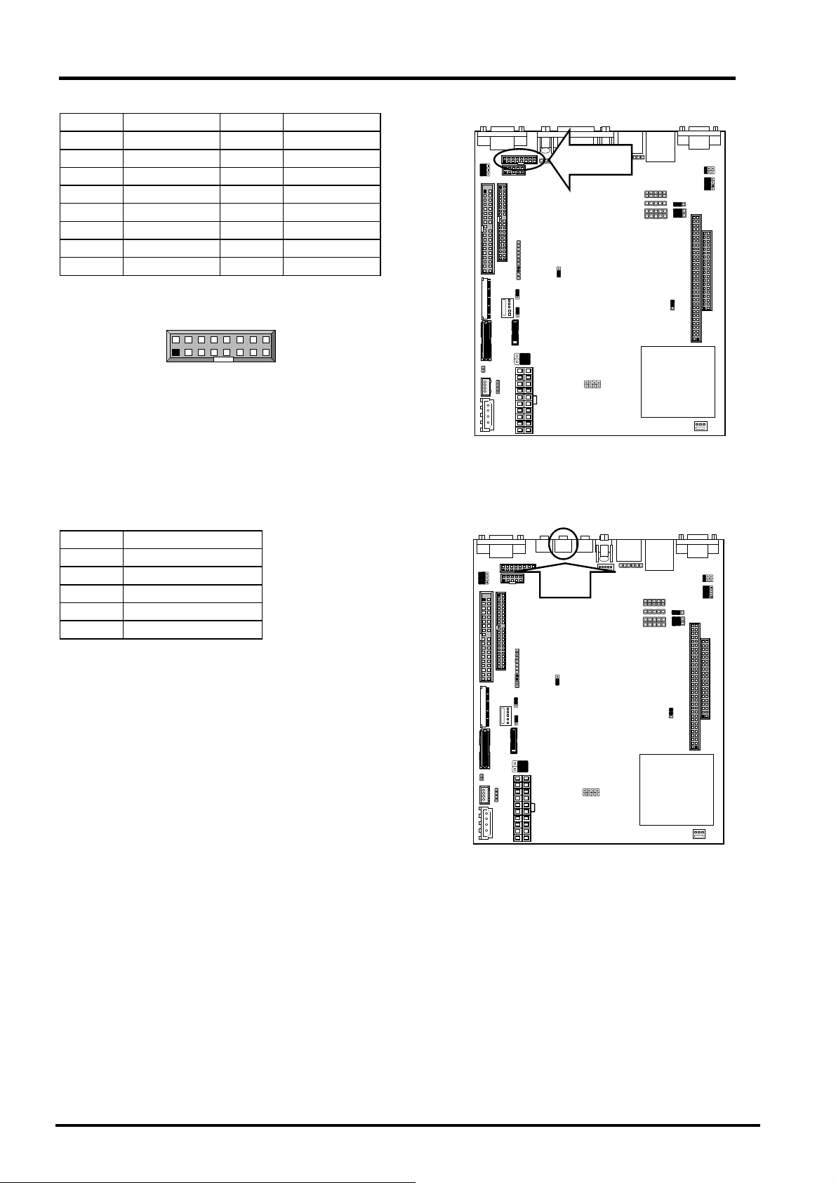
!"VGAC1: Internal VGA Connector
Pin No. Description Pin No. Description
1 R 2 GND
3 G 4 GND
5 B 6 GND
7 GND 8 GND
9 GND 10 HSYNC
11 GND 12 VSYNC
13 GND 14 D2 DATA
15 GND 16 D2 CLK
!"MIC1: MIC IN 5Pin-PHONE Jack
Pin No. Description
1 CO_GND
2 MIC_IN
3 CO_GND
4 CO_GND
5 Pull High
2 16
1 15
GAC1
2X8 Pin 2.54mm Pitch Header
︵
︵
︵
︵
︶
︶
︶
︶
GAC1
MIC1
28
User’s Manual
Page 33
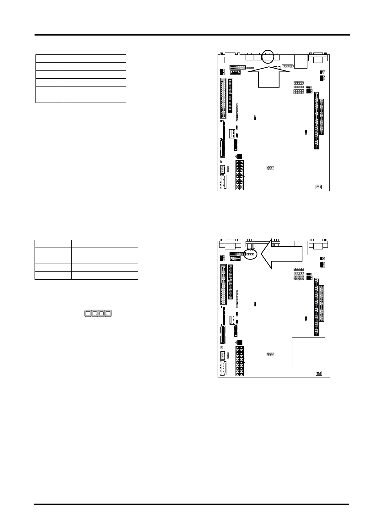
!"LNI1: Line IN 5Pin-PHONE Jack
Pin No. Description
1 CO_GND
2 LIN-L
3 CO_GND
4 CO_GND
5 LIN-R
!"CDIN 1: CD_IN Connector
Pin No. Description
1 CDL
2 CD_GND
3 CD_GND
4 CDR
1
CDIN1
4
Chapter 2 Installation
LNI1
CDIN1
User’s Manual
29
Page 34
Chapter 2. Installation
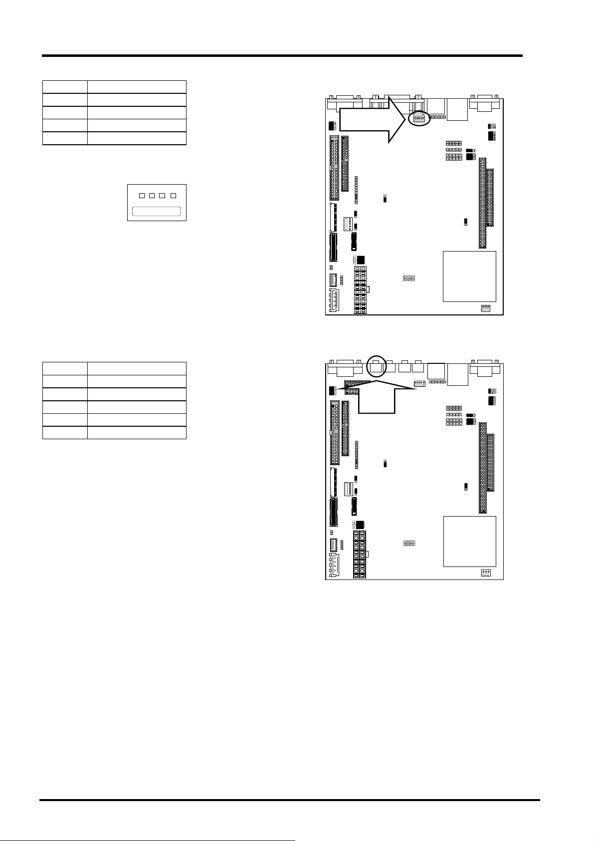
!"ISPKR1: Internal speaker connector
Pin No. Description
1 South-L
2 GND
3 GND
4 Sout-R
1 4
ISPKR1
!"LNO1: Line out 5Pin-PHONE Jack
Pin No. Description
1 CO_GND
2 LOT_L
3 NC
4 NC
5 LOT_R
Wafer 1x4 2.54mm
︵
︵
︵
︵
︶
︶
︶
︶
ISPKR1
LNO1
30
User’s Manual
Page 35
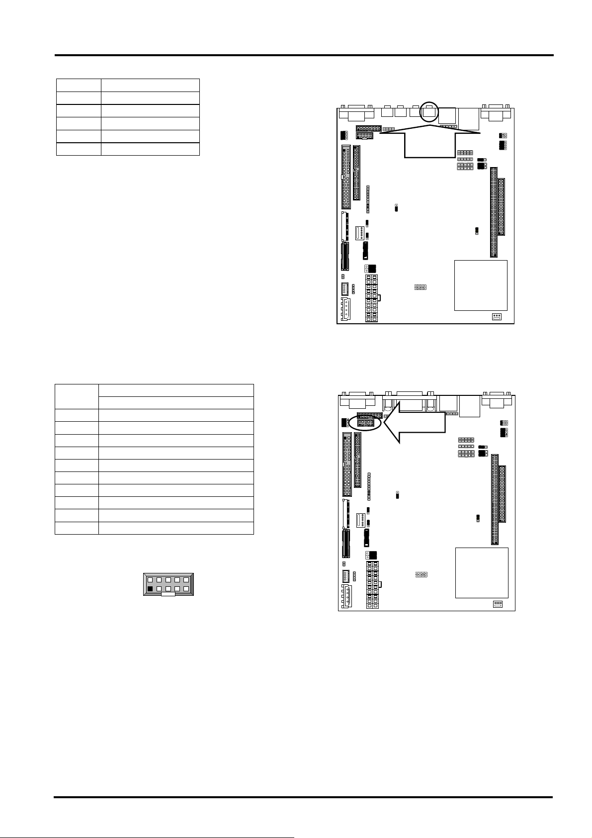
!"SP EA K1 : Head er pho ne c onn ec t or 5Pin-PHONE Jack
Pin No. Description
1 CO_GND
2 AUD-L
3 NC
4 NC
5 AUD-R
!"COMB1: Serial Port #4 Connector (Header)
Pin No.
Description
RS-232
1 Data Carrier detect (DCD4#)
2 Data Set Ready (DSR4#)
3 Receive Data (RXD4)
4 Request To Send (RTS4#)
5 Transmit Data (TXD4)
6 Clear To Send (CTS4#)
7 Data Terminal Ready (DTR4)
8 Type Select4
9 Ground
10 Key
2
10
1
COMB1
9
Chapter 2 Installation
SPEAK1
COMB1
User’s Manual
31
Page 36

Chapter 3 BIOS Setup
Chapter 3 BIOS Setup
Award‘s ROM BIOS provides a built-in Setup program that allows users to modify the basic system
configuration and settings. The modified data will be stored in a battery-backed CMOS RAM so that this
data will be retained even when the power is turned off. In general, the information saved in the CMOS
RAM remains unchanged unless there is a configuration change in the system, such as hard drive
replacement or new equipment installment.
3.1 Running AWARD BIOS
The Setup Utility is stored in the BIOS ROM. When the power of the computer system is turned on, a
screen message will appear to give you an opportunity to call up the Setup Utility while the BIOS will
enter the Power On Self Test (POST) routines. The POST routines perform various diagnostic checks
while initializing the board hardware. If the routines encounter an error during the tests, the error will
be reported in one of two ways, a series of short beeps or a n error message on the screen. There are
two kinds of errors, fatal and non-fatal. The system can usually continue the boot up sequence with
non-fatal errors. Non-fatal error messages usually appear on the screen along with the following
instructions:
“ Press <F1> to RESUME ”
Write down the message and press the F1 key to continue the boot up sequence. After the POST
routines are completed, the following message appears:
“ Press DEL to enter SETUP ”
Entering Setup
Turn on the power of the computer system and press <Del> immediately. If you don’t have the chance
to respond, reset the system by simultaneously pressing the <Ctrl>, <Alt> and <Delete> keys, or by
pushing the ‘ Reset ’ button on the system cabinet. You can also restart by turning the system OFF then
ON.
32
User’s Manual
Page 37

Chapter 3 BIOS Setup
3.2 CMOS Setup Utility
To access the AWARD BIOS SETUP program, press the <DEL> key. The screen display will appears as
shown below:
Main Program Screen
! Standard CMOS Features ! PC Health Status
! Advanced BIOS Features Load Optimized Defaults
! Advanced Chipset Features Set Supervisor Password
! Integrated Peripherals Set User Password
! Power Management Setup Save & Exit Setup
! PnP/PCI Configurations Exit Without Saving
Esc : Quit
F10 : Save & Exit Setup
Phoenix - Award BIOS CMOS Setup Utility
# $ %
Time, Date, Hard Disk Type...
: Select Item
This screen provides access to the utility‘s various functions.
Listed below is explanation of the keys displayed at the bottom of the screen:
<ESC>: Exit the utility.
<#### $$$$ %%%% &&&&>: Use arrow keys # $ % & to move cursor to your desired selection.
<F1> : General Help
<F10>: Saves all changes made to Setup and exits program.
User’s Manual
33
Page 38

Chapter 3 BIOS Setup
Standard CMOS Setup: Use this menu for basic syst em configurations.
Advanced BIOS Features: Use this menu to set the Advanced Features available on your system.
Advanced Chipset Features: Use this menu to change the values in the chipset registers and optimizes
your system’s performance.
Integrated Peripherals: Use this menu to specify your settings for integrated peripherals.
Power Management Setup: Use this Menu to specify your settings for power management.
PnP/PCI Configurations: This entry appears if your system supports PnP/PCI.
PC Health Status: This entry shows your PC health status. If Hardware Monitor Chipset is installed.
Load Optimized Defaults: Use this menu to load the BIOS default values that are factory settings for
optimal performance system operations.
Set Supervisor Password: Use this menu to set Supervisor Passwords.
Set User Passwor d: Use this menu to set User Passwords.
Save & Exit Setup: Save CMOS value changes to CMOS and exit setup.
Exit Without Saving: Abandon all CMOS value changes and exit setup.
34
User’s Manual
Page 39

Chapter 3 BIOS Setup
3.3 Standard CMOS Setup
When you select the “STANDARD CMOS SETUP” on the main program, the screen display will appears as:
Standard CMOS Setup Screen
Phoenix - Award BIOS CMOS Setup Utility
Standard CMOS Features
Date (mm:dd:yy) Mon, Feb 17, 2003 Item Help
Time ( hh:mm:ss) 13 : 25 : 38 Menu Level !
! IDE Prima ry Master [IBM-DPTA-372050]
! IDE Primary Slave [None]
! IDE Secondary Master [IDE/ATAPI CD-ROM 50X]
! IDE Secondary Slave [None]
Drive A [1.44M, 3.5 in.]
Drive B [None]
Halt On [All Errors]
Base Memory 640K
Extended Memory 228352K
Total Memory 229376K
# $ % Move Enter: Select +/-/PU/PD: Value F10: Save ESC: Exit F1: General Help
F5: Previous Values F7:Optimized Defaults
Change the day, month,
year and century
The Standard CMOS Setup utility is used to configure the following compo nents such as date, time, hard
disk drive, floppy drive, display and memory. Once a field is highlighted, on-line help information is
displayed in the left bottom of the Menu screen.
Set Date: Month, Date, and Year.
Set Time: Hour, Minute and Second. Use 24-hour clock format (for p.m. time, add 12 to the hour
number, e.g. you would en ter 4:30 p.m. as 1 6:30). When you select the “STANDARD CMOS SETUP” on
the main program, the screen display will appears as:
User’s Manual
35
Page 40

Chapter 3 BIOS Setup
Primary Master / Primary Slave
Secondary Master / Secondary Slave: Press PgUp / <+> or PgDn / <- > to s elect M anual, No ne, Aut o
type. Note that the specifications of your drive must match with the drive table. The hard disk will not
work properly if you enter improper information for this category. If your hard disk drive type is not
matched or listed, you can use Manual to define your own drive type manually.
If you select Manual, related information is asked to be entered to the following items. Enter the
information directly from the keyboard. This information should be provided in the documentation from
your hard disk vendor or the system manufacturer.
If the controller of HDD interface is SCSI, the selection shall be
“None”
If the controller of HDD interface is CD-ROM, the selection shall be
“None”
Here is a brief explanation of drive specifications:
!" Access Mode: The settings are Auto, Normal, Large, and LBA.
!" Cylinder: Number of cylinders
!" Head: Number of head s
!" Precomp: Write precom
!" Landing Zone: Landing Zone
!" Sector: Number of sectors
Drive A and Drive B: Select the correct specifications for the diskette drive(s) installed in the computer.
None No diskette drive installed
360K, 5.25 in 5-1/4 inch PC-type standard drive; 360 kilobyte capacity
1.2M, 5.25 in 5-1/4 inch AT-type high-density drive; 1.2 megabyte capacity
720K, 3.5in 3 1-2 inch double-sided drive; 720 kilobyte capacity
1.44M, 3.5 in 3 1-2 inch double-sided drive; 1.44 megabyte capacity
2.88M, 3.5 in 3 1-2 inch double-sided drive; 2.88 megabyte capacity
Note: 1. Not Installed could be used as an option for diskless workstations.
36
2. Highlight the listing after each drive name and select the appropriate entry.
User’s Manual
Page 41

Chapter 3 BIOS Setup
Halt On: During the power-on-self-test (POST), the computer stops if the BIOS detect a hardware error.
You can tell the BIOS to ignore certain errors POST and continue the boot-up process. These are the
selections:
No errors Whenever the BIOS detects a non-fatal error the system will not be
stopped and you will be prompted
All errors The system boot will be stopped for any error that may be detected.
All, But Keyboard The system boot will not stop for a keyboard error; it will stop for all
Other errors.
All, But Diskette The system boot will not stop for a disk error; it will st op for all other
Errors.
All, But Disk/Key The system boot will not stop for a keyboard or disk error; it will stop
for all other errors.
User’s Manual
37
Page 42

Chapter 3 BIOS Setup
3.4 BIOS Features Setup
When you select the “BIOS FEATURES SETUP” on the main program, the screen display will appear as:
BIOS Features Setup Screen
Virus Warning
Quick Power On Self Test
First Boot Device
Second Boot Device
Third Boot Device
Boot Other Device
Swap Floppy Drive
Hard Disk Write Protect
Floppy Disk Access Control
Boot Up NumLock Status
Security Option
PS/2 Mouse Support
HDD S.M.A.R.T Capability
Video BIOS Shadow
C8000 - CBFFF Shadow
CC000 - CFFFF Shadow
D0000 - D3FFF Shadow
D4000 - D7FFF Shadow
D8000 - DBFFF Shadow
DC000 - DFFFF Shadow
Full Screen LOGO Show
Phoenix - Award BIOS CMOS Setup Utility
Advanced BIOS Features
[Disabled]
[Enabled]
[Floppy]
[HDD-0]
[CDROM]
[Enabled]
[Disabled]
[Disabled]
[R/W]
[On]
[Setup]
[Enabled]
[Enabled]
[Enabled]
[Disabled]
[Disabled]
[Disabled]
[Disabled]
[Disabled]
[Disabled]
[Disabled]
"
Menu Level !
Allow you to choose the
VIRUS warning feature
for IDE Hard Disk boot
sector protection. If this
function is enabled and
someone attempt to
write data into this area,
BIOS will show a
warning message on
screen and alarm beep
#
Item Help
# $ % Move Enter: Select +/-/PU/PD: Value F10 : Save Esc: Exit F1: General Help
F5: Previous Values F7: Optimized Defaults
The following explains the options for each of the features as listed in the above menu:
Virus Warning: The default setting of Virus Warning is “Disabled”. When it is enabled, any attempt to
write the boot sector and partition table will halt the system and cause a warning message to appear. If
this happens, you can use a n anti-virus utility on a vir us free, bootable floppy diskette to reboot , to clean
and to investigate your system.
Quick Power On Self-Test: The default setting is “Enabled”. This speeds up the Power On Self Test
(POST) by skipping some items that are normally checked during the full POST. If your system is
functioning normally, you can choose this feature to speed up the booting process.
38
User’s Manual
Page 43

Chapter 3 BIOS Setup
First / Second / Third / Other Boot Device: The BIOS attempts to load the operating system from the
devices in the sequence selected in these items. The settings are Floppy, LS/ZIP,
HDD-0/HDD-1/HDD- 2/HD D -3, SCSI, C DRO M, LAN, and Disabled .
Swap Floppy Drive: The default setting is “Disabled”. This setting gives you an option to swap A and B
floppy disks. Normally, the floppy drive A is the one at the end of the cable and drive B is at the other
end. If you set this option to “Enabled”, the Drive A will function as Drive B, and vice-versa under the
DOS.
Hard Disk Write Protect: This option specifies the write protect function of Hard Disk Drive.
Floppy Disk Access Cont rol: This option specifies the read/write access that is set when booting from a
floppy drive.
Boot Up NumLock Status: The default setting is “On”. If it set “Off” the cursor controls will function on
the numeric keypad.
Security Op tion: This setting controls the password in the main screen. The options are “Setup” and
“System”. Select “Setup” and it will protect the Setup Utility settings from being tampered with. Select
“System” if you want to use password feature every time the system boots up. The default setting is
“Setup”. You can create your password by using the “SUPERVISOR /USER PASSWORD” utility on the main
program screen.
PS/2 Mouse Support: This option enable Award BIOS support for a PS/2-type mouse.
HDD S.M.A.R.T Capability : SMART (Self-Monitoring, Analysis, and Reporting Technology) is a technology
developed to manage disk drive reliability by predicting device failures. Award BIOS can warn of possible
device failure, allowing time for backups or drive replacement.
Video BIOS Shadow: Th e default setting is “Enable d” which will copy the VGA display card BIOS into
system DRAM to improve performance.
C8000-CBFFF Shadow to DC000-DFFFF Shadow: The default setting for the shadow feature is
“Disabled”. When enabled, the ROM wit h the specific address is copied into system DRAM. It will also
reduce the size of memory available to the system. After you have made your selection in the BIOS
FEATURES SETUP, press the <ESC> key to go back to the main program screen.
User’s Manual
39
Page 44

Chapter 3 BIOS Setup
3.5 Chipset Features Setup
When you select the “CHIPSET FEATUR ES SETUP” on the main program, the screen display will appears
as:
Chipset Features Setup Screen
Phoenix - Award BIOS CMOS Setup Utility
Spread Spectrum
DRAM Timing By SPD
Memory Hole
P2C/C2P Concurrency
System BIOS Cacheable
Video RAM Cacheable
Frame Butter Size
AGP Aperture Size
AGP-4X Mode
AGP Driving Control
AGP Driving Value
X
Panel Type
CPU to PCI Write Buffer
PCI Dynamic Bursting
PCI Master 0 WS Write
PCI Delay Transaction
PCI#2 Access #1 Retry
AGP Master 1 WS Write
AGP Master 1 WS Read
Advanced Chipset Features
[Disabled]
[Enabled]
[Disabled]
[Enabled]
[Enabled]
[Enabled]
[8M]
[64M]
[Enabled]
[Auto]
[DA]
[1024!768 TFT 65Mhz]
[Enabled]
[Enabled]
[Enabled]
[Disabled]
[Enabled]
[Disabled]
[Disabled]
Item Help
Menu Level !
# $ % Move Enter: Select +/-/PU/PD: Value F10: Save Esc: Exit F1: General Help
F5: Previous Values F7: Optimized Defaults
Spread Spectrum: When the system clock generator pulses, the extreme values of the pulse generate
excess EMI. Enabling pulse spectrum spread modulation changes the extreme values from spikes to flat
curves, thus reducing EMI. This benefit may in some cases be outweighed by problems with timing-critical
devices, such as a clock-sensitive SCSI device.
DRAM Timing By SPD: This item allows you to select the value in this field, depending on whether the
board has paged DRAMs or EDO (extended data output) DRAMs.
Memory Hole: In order to improve performance, certain space in memory ca n be reserved for ISA cards.
This memory must be mapped into the memory space below 16MB.
Enabled Memory hole supported
Disabled (default) Memory hole not supported
40
User’s Manual
Page 45

Chapter 3 BIOS Setup
P2C / C2P Concurrency: This item allows you to Enable or Disable the PCI to CPU, CPU to PCI
concurrency. The default setting is “Enabled”.
System BIOS Cacheable: Selecting “Enabled” allows caching of the system BIOS ROM at F0000h FFFFFh, resulting in better system performance. However, if any program writes to this memory area, a
system error may result. The settings are “Enabled” and “Disabled”.
Video RAM cacheable: The choices: Enabled, Disabled (Default).
Frame Butter Size: The choices: 2M, 4M, 8M(Default), 16M, and 32M.
AGP Aperture Size: Select the size of the Accelerated Graphics Port (AGP) aperture. The aperture is a
portion of the PCI memory address range dedicated for graphics memory address space. Host cycles that
hit the aperture range are forwarded to the AGP without any translation.
AGP!!!!4X Mode: Setting AGP rate to 4X or 2X.
AGP Driving Control: This item allows you to adjust the AGP driving force. Choose Manual to key in an
AGP Driving Value in the next selection. This field is recommended to set in “Auto” for avoiding any error
in your system. The default setting is “Auto”.
AGP Driving Value: This item allows you to adjust the AGP driving force.
Panel Type: Please select the type of panel you are incorporating with our single board computer. Consult
your panel manual for detail information.
CPU to PCI Write Buffer : When this field is “Enabled”, writes from the CPU to the PCI bus is buffered,
to compensate for the differences between the CPU and the PCI bus. When disabled, the writes are not
buffered and the CPU must wait until the write is complete before starting another cycle. The default
setting is “Enabled”.
PCI Dynamic Bursting: This item allows you to enable or disable the PCI dynamic bursting function.
The settings are “Enabled” or “Disabled”.
User’s Manual
41
Page 46

Chapter 3 BIOS Setup
PCI Master 0 WS Write: When enabled, writes to the PCI bus and are executed with zero wait states.
The settings are “Enabled” or Disabled”.
PCI Delay Transaction: The chipset has an embedded 32-bit posted write buffer to support delay
transactions cycles. Select “Enabled” to support compliance with PCI specification version 2.1. The
settings are “Enabled” or “Disabled”.
PCI#2 Access #1 Retry: When disabled, PCI#2 will not be discon nected until access finishes. When
enabled, PCI#2 will be disconnected if max retries are attempted without success. The default setting is
“Enabled”.
AGP Master 1 WS Write: Implements a single delay when writing from the AGP Bus. Normally, two wait
states are used, allowing for greater stability, but check with your motherboard manufacturer to see if they
have already implemented a Master latency of zero, in which case the lowest writing here of 1 will reduce
performance.
AGP Master 1 WS Read: Implements a single delay when reading from the AGP Bus. Normally, two wait
states are used, allowing for greater stability, but check with your motherboard manufacturer to see if they
have already implemented a Master latency of zero, in which case the lowest reading here of 1 will reduce
performance.
42
User’s Manual
Page 47

Chapter 3 BIOS Setup
3.6 Integrated Peripherals
When you select the “INTEGRATED PERIPHERIALS” on the main program, the screen display will appears
as:
Integrated Peripherals Setup Screen
Phoenix – Award BIOS CMOS Setup Utility
Integrated Peripherals
On-Chip Primary PCI IDE
On-Chip Secondary PCI IDE
USB Controller
USB Keyboard Support
AC97 Audio
Init Display First
Onboard FDD Controller
Onboard Serial Port 1
Onboard Serial Port 2
UART 2 Mode
X
IR Function Duplex
X
TX, RX inverting enable
Onboard Parallel Port
Parallel Port Mode
X
ECP Mode Use DMA
X
Parallel Port EPP Type
Onboard Serial Port 3
Serial Port 3 Use IRQ
Onboard Serial Port 4
Serial Port 4 Use IRQ
Onboard Legacy Audio
X
Sound Blaster
[Enabled]
[Enabled]
[Enabled]
[Disabled]
[Auto]
[Add-On Card]
[Enabled]
[3F8/IRQ4]
[2F8/IRQ3]
[Standard]
Half
No, Yes
[378/IRQ7]
[Normal]
3
Epp1.9
[3E8H]
[IRQ4]
[2E8H]
[IRQ3]
[Enabled]
[Enabled]
"
#
Item Help
Menu Level !
# $ % Move Enter: Select +/-/PU/PD: Value F10: Save Esc: Exit F1: General Help
F5: Previous Values F7: Optimized Defaults
On-Chip Primary PCI IDE: The chipset contains a PCI IDE interface with support for two IDE channels.
Select Enabled to activate the primary IDE interface. Select Disabled to deactivate this interface. The
settings are “Enabled” and “Disabled”.
On-Chip Secondary PCI IDE: The chipset contains a PCI IDE interface with support for two IDE
channels. Select Enabled to activate the secondary IDE interface. Select Disabled to deactivate this
interface. The settings are “Enabled” and “Disabled”.
USB Controller: Select Enabled if your system contains a Universal Serial Bus (USB) controller and you
have USB peripherals
USB Keyboard Sup port: Set this option to “Enable d” or “Disabled” the USB keyboard/ mouse support.
The default setting is “Disabled”.
AC97 Audio: This option sets the AC97 Audio.
User’s Manual
43
Page 48

Chapter 3 BIOS Setup
Init Display First: This item allows you to decide to active whether PCI Slot of VGA card or AGP first.
The settings are “PCI Slot” and “AGP Slot”.
Onboard FDD Controller: Select Enabled if your system has a flopp y disk controller (FDC) installed on
the system board and you want to use it. If you install add-in FDC or the system has no floppy drive,
select Disabled in this field. The settings are “Enabled” and “Disabled”.
Onboard Serial Port 1 / Port 2: Select an address and corresponding interrupt for the first and second
serial ports. The settings a re “3F8/IRQ4”, “ 2E8/IRQ3”, “3E8/IRQ4”, “2F8/IRQ3”, “Disabled”, “Auto”.
UART 2 Mod e: This item allows you to select which mode for the Onboard Serial Port 2. The settings
are “Standard”, “HPSIR”, and “ASKIR”.
IR Function Duplex: This item allows you to select the IR half/full duplex function.
TX, RX inverting enable: This item allows you to enable the TX, RX inverting which depends on different
H/W requirement. This field is not recommended to change its default setting for avoiding any error in
your system.
Onboard Parallel Port: This item allows you to determine onboard parallel port controller I/O address
setting. The settings are “378H/IRQ7”, “278H/IRQ5”, “3BC/IRQ7”, and “ Disabled”.
Parallel Port Mode: There are four options “Normal” (default), “ECP”, “ECP/EPP” and “EPP/SPP”.
Change the mode from “Normal” to the enhanced mode only if your peripheral device can support it.
When it is set to ECP mode, the printer port always uses DMA3.
ECP Mode Use DMA: Sel ect a DMA channel for the parallel port for use during ECP mode. The settings
are “3” and “1”.
Parallel Port EPP Type: Select EPP port type 1.7 or 1.9.
Onboard Serial Port 3: The choices: Disabled (Default), 3F8, 2F8, 3E8, and 2E8.
Serial Port 3 Use IRQ: The choices: IRQ10, IRQ11, IRQ4, IRQ3.
Onboard Serial Port 4: The choices: Disabled ( Default), 3F8, 2F8, 3E8, and 2E8.
Serial Port 4 Use IRQ: The choices: IRQ10, IRQ11, IRQ4, IRQ3.
Onboard Legacy Audio: This option let you enable or disable the onboard Legacy Audio function.
Sound Blaster: This option let you enable or disable the onboard Sound Blaster function.
44
User’s Manual
Page 49

Chapter 3 BIOS Setup
3.7 Power Management Setup
The “Power Management Setup” controls the CPU card‘s “Green” features. When you select the
“POWER MANAGEMENT SETUP” on the main program, the screen display will appears as:
Power Management Setup Screen
ACPI function [Disabled] Item Help
Power Management [Min Saving] Menu Level !
Video Off Option [Suspend -> Off]
Video Off Method [V/H SYNC + Blank]
Suspend Mode 1 Hour
HDD Power Down [Disabled]
LPT & COM [Disabled]
Power On by LAN/Ring [Disabled]
Power On by RTC Alarm [Disabled]
X Date (of Month) 0
X Resume Time (hh:mm:ss) 0 : 0 : 0
PwrOn After AC Power Loss [On]
Phoenix – Award BIOS CMOS Setup Utility
Power Management Setup
# $ % Move Enter: Select +/-/PU/PD: Value F10: Save Esc: Exit F1: General Help
F5: Previous Values F7: Optimized Defaults
ACPI Function: This item allows you to enable or disable the Advanced Configuration and Power
Management (ACPI). The settings are “Enabled” and “Disabled”.
User’s Manual
45
Page 50

Chapter 3 BIOS Setup
Power Management:
Min. Power Saving Minimum power management. Doze Mode=1hr. Standby Mode =1hr.,
Suspend Mode=1hr., and HDD Power Down=15min.
Max. Power Saving Maximum power management. –Only available for SL CPU’s. Doze
Mode=1min., Standby Mode=1min., Suspend Mode=1min., and HDD Power
Down=1min.
User De fined Allow you to set each mode individually. When not disabled, each of the
ranges is from 1 min. to 1 hr. except for HDD Power Down, which ranges
from 1 min. to 15 min. and disabled.
Video Off Option: This option is for choosing the setting in whi ch the monitor will turn off. The default
setting is “Suspend”.
Always On Always turn on.
Suspend During Suspend mode, the monitor will be turned off.
All Modes During All Modes mode, the monitor will be turned off.
Video Off Method : This determines the manner in which the monitor is blanked. The default setting is
“V/H SYNC+Blank”.
V/H SYNC+Blank This selection will cause the system to t urn off the vertical and horizontal
synchronization ports and write blank to the video buffer.
Blank Screen This option only writes blanks to the video buffer.
DPMS Initial display power management signaling.
Suspend Mode: Power saving by suspends mode setting.
HDD Power Down: Options are from “1 Min”. to “15 Min”. and “Disable”. The IDE hard drive will spin
down if it is not accessed within a specified length of ti me.
LPT & COM: Print Port and COM Port turn on/off.
Power On by LAN/Ring: When Enabled, an input signal on the serial LAN/Ring Indicator (RI) line (in
other words, an incoming call on the modem) awakens the system from a soft off state.
Power On by RTC Alarm: Power-on interval by RTC setting.
PwrOn After AC Power Loss: This option specifies the Power ON/OFF Status after AC power loss.
46
User’s Manual
Page 51

Chapter 3 BIOS Setup
3.8 PnP/PCI Configuration
Both the ISA and PCI buses on the CPU card use system IRQs & DMAs. You must set up the IRQ and
DMA assignments correctly through the PnP/PCI Configuration Setup utility; otherwise the motherboard
will not work properly.
PnP/PCI Configuration Setup Screen
Phoenix – Award BIOS CMOS Setup Utility
PnP/PCI Configurations
PNP OS Installed [No] Item Help
Reset Configuration Data [Disabled] Menu Level !
Resources Controlled By [Manual]
! IRQ Resources [Press Enter]
! DMA Resources [Press Enter]
! Memory Resources [Press Enter]
PCI/VGA Palette Snoop [Disabled]
PCI Latency Timer (CLK) [32]
INT Pin 1 Assignment [Auto]
INT Pin 2 Assignment [Auto]
INT Pin 3 Assignment [Auto]
INT Pin 4 Assignment [Auto]
# $ % Move Enter: Select +/-/PU/PD: Value F10: Save Esc: Exit F1: General He lp
F5: Previous Values F7: Optimized Defaults
PNP OS Installed: When set to “Yes”, BIOS will o nly initialize the PnP cards use d for booting (VGA, IDE,
Select Yes if you are
using a Plug and Play
capable operating
system. Select No if
you need the BIOS to
configure non-boot
devices.
SCSI). The rest of the cards will be initialized by the PnP operating system like Windows® 95 or 98.
When set to “No”, BIOS will initialize all the PnP cards. So, for non-PnP operating system (DOS,
Netware®), this option must set to “Yes”.
Reset Configuration Data: Normally, you leave this field “Disabled”, Select “En abled” to reset Extended
System Configuration Data (ESCD) when you exit Setup if you have installed a new add-on and the system
reconfiguration has caused such a serious conflict that the operating system cannot boot.
The settings are: “Enabled and Disabled”.
User’s Manual
47
Page 52

Chapter 3 BIOS Setup
Resource Controlled By: The Award Plug and Play BIOS has the capacity to automatically configure all
of the boot and Plug and Play compatible devices. However, this capability means absolutely nothing
unless you are using a Plug and Play operating system such as Windows98. If you set this field to
“Manual” choose specific resources by going into each of the sub menu that follows this field (a sub menu
is proceeded by a “”). The settings are “Auto (ESCD)”, “Manual”.
IRQ Resources: When resources are controlled manually, assign each system interrupt as one of the
following types, depending on the type of device using the interrupt.
IRQ-3 assigned to
IRQ-4 assigned to
IRQ-5 assigned to
IRQ-7 assigned to
IRQ-9 assigned to
IRQ-10 assigned to
IRQ-11 assigned to
IRQ-12 assigned to
IRQ-14 assigned to
IRQ-15 assigned to
[Legacy ISA]
[Legacy ISA]
[PCI /ISA PNP]
[Legacy ISA]
[PCI /ISA PNP]
[PCI /ISA PNP]
[PCI /ISA PNP]
[PCI /ISA PNP]
[PCI /ISA PNP]
[PCI /ISA PNP]
Menu Level
Legacy ISA for devices
compliant with the original PC
AT bus specification, PCI/ISA
PnP for devices compliant with
the Plug and Play standard
whether designed for PCI or
ISA bus architecture.
Item Help
DMA Resources: The sub menu can let you control the DMA resource.
DMA-0 assigned to
DMA-1 assigned to
DMA-3 assigned to
DMA-5 assigned to
DMA-6 assigned to
DMA-7 assigned to
[PCI /ISA PnP]
[PCI /ISA PnP]
[PCI /ISA PnP]
[PCI /ISA PnP]
[PCI /ISA PnP]
[PCI /ISA PnP]
Menu Level
Legacy ISA for devices
compliant with the original PC
AT bus specification, PCI/ISA
PnP for devices compliant with
the Plug and Play standard
whether designed for PCI or
Item Help
ISA bus architecture.
Memory Resources:
This option specifies the size of the memory area reserved for legacy ISA adapter cards.
PCI/VGA Palette Snoo p: Leave this field at “Disabled”. The settings are “Enabled”, “Disabled”.
PCI Latency Timer (CLK): This option specifies the latency timings (in PCI clocks) for PCI devices
installed in the PCI expansion slots.
The Latency Timer limits the time that device can hold the PCI bus. The timer starts when the device gains
bus ownership, and counts down at the rate of the PCI clock. When the counter reaches zero, the device is
required to release the bus.
48
User’s Manual
Page 53

Chapter 3 BIOS Setup
INT Pin 1/2/3/4 Assignment: These options specify the IRQ priority for PCI devices installed in the PCI
expansion slots.
3.9 PC Health Status (Optional)
This section helps you to get more information about your system in cluding CPU temperature, FAN speed
and voltages. It is recommended that you contact your motherboard supplier to get proper value about
your setting of the CPU temperature.
Phoenix – Award BIOS CMOS Setup Utility
PC Health Status
CPU Temperature.
System Temperature
FAN1 0 RPM
Vcore 1.17 V
+2.5V 2.47 V
+3.3V 3.25 V
+5V 5.02 V
# $ % Move Enter: Select +/-/PU/PD: Value F10: Save Esc: Exit F1: General Help
F5: Previous Values F7: Optimized Defaults
CPU Temperature: This item shows the CPU temperature.
System Temperature: This item displays the value of system temperature.
FAN1: This item displays the value of FAN1 speed.
51℃/ 123℉
30℃/ 86℉
Item Help
Menu Level !
Vcore: This item shows the current system voltage.
User’s Manual
49
Page 54
Chapter 3 BIOS Setup
3.10 Load Optimized Defaults
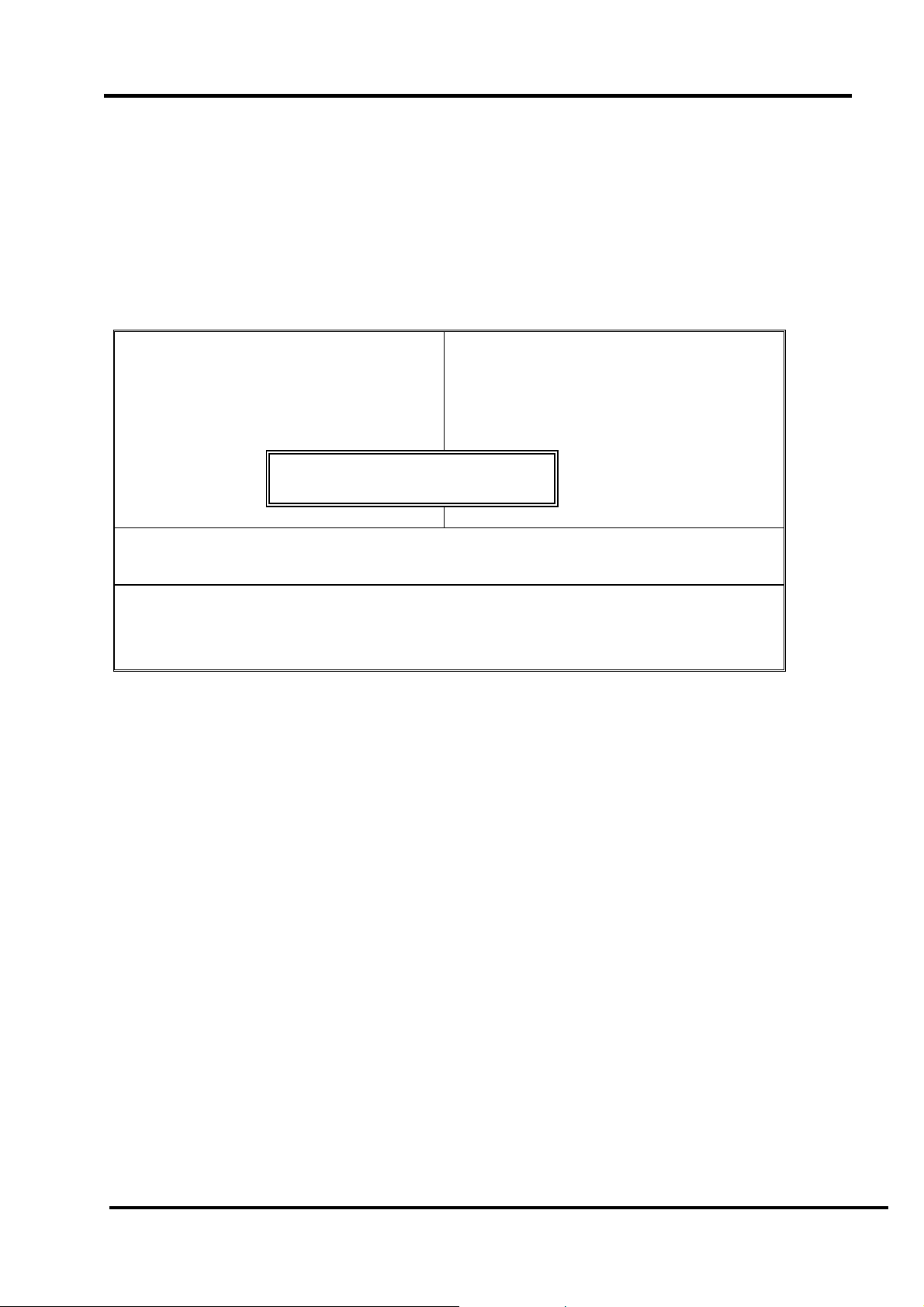
When you press “Enter” on this item, you get a confirmation dialog box with a message similar to:
Load Optimized Defaults (Y/N)? N
Pressing “Y” loads the default values that are factory settings for optimal performance system operations.
Phoenix – Award BIOS CMOS Setup Utility
!Standard CMOS Features
!Advanced BIOS Features
!Advanced Chipset Features
!Integrated Peripherals
!Power Management
Load Optimized Defaults (Y/N)? N
!PnP / PCI Configure
ESC: Quit # $ % : Select Item
F10: Save & Exit Setup
Load Optimized Defaults
!PC Health Status
Load Optimized Defaults
Set Supervisor Password
Set User Password
setup
Saving
50
User’s Manual
Page 55
Chapter 3 BIOS Setup
3.11 Set Supervisor / User Password
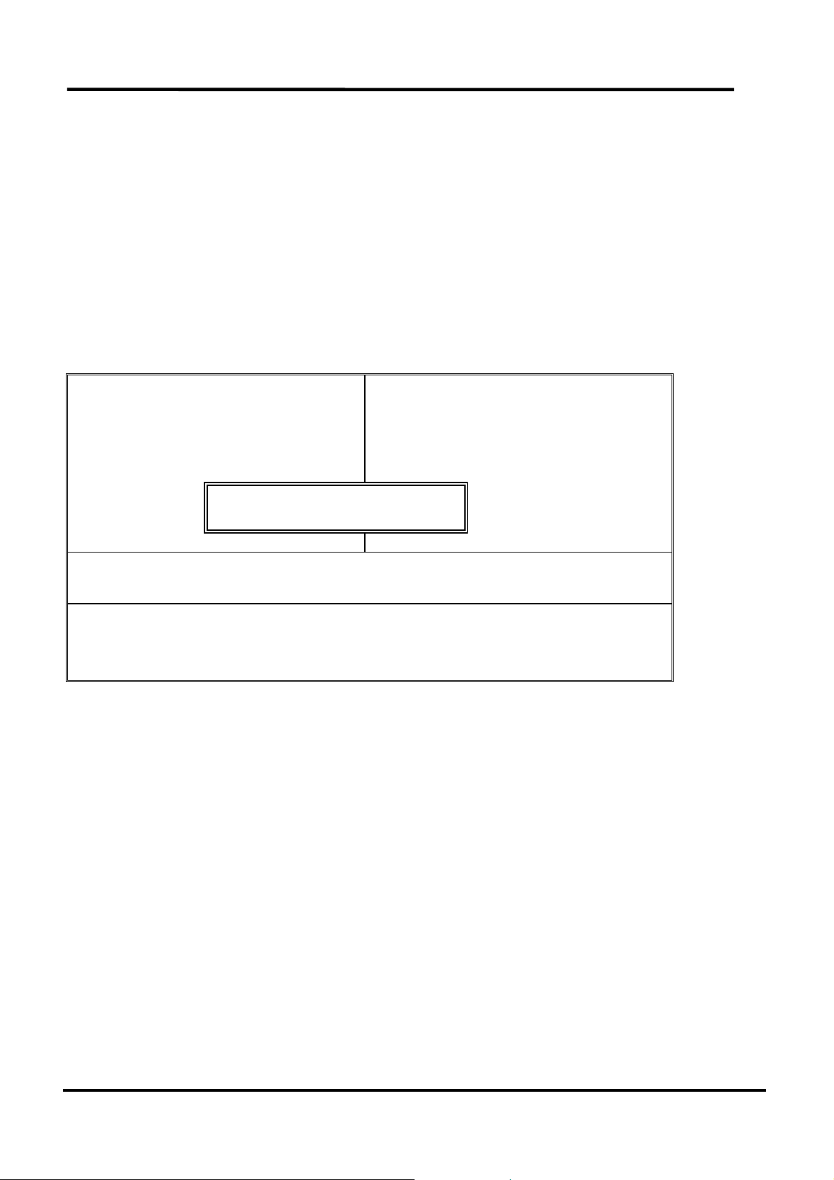
The “SUPERVISOR/USER PASSWORD” utility sets the password. The SBC is shipped with the password
disabled. If you want to change the password, you must first enter the current password, and then at the
prompt -- enter your new password. The password is case sensitive, and can be up to 8 alphanumeric
characters. Press <Enter> after you have finished typing in the password. At the next prompt, confirm
the new password by re-typing it and pressing <Enter> again. When you are done, the screen
automatically reverts to the main screen. Remember that when you use this feature, the “Security
Option” line in BIOS FEATURES SETUP will determine when entering the password will be required.
Phoenix – Award BIOS CMOS Setup Utility
!Standard CMOS Features
!Advanced BIOS Features
!Advanced Chipset Features
!Integrated Peripherals
!Power Management
Enter Password:
!PnP / PCI Configure
ESC: Quit # $ % : Select Item
F10: Save & Exit Setup
Change/Set/Disable Password
To disable the password, press the <Enter> key instead of entering a new password when the “Enter
Password” in the dialog box appears. A message will appear confirming that the password is disabled.
!PC Health Status
Load Optimized Defaults
Set Supervisor Password
Set User Password
setup
Saving
If you have set both supervisor and user password, only the supervisor passwor d allows you to enter the
BIOS SETUP PROGRAM.
Note: If you forget your password, the only way to solve this problem is to discharge the CMOS memory.
User’s Manual
51
Page 56
Chapter 3 BIOS Setup
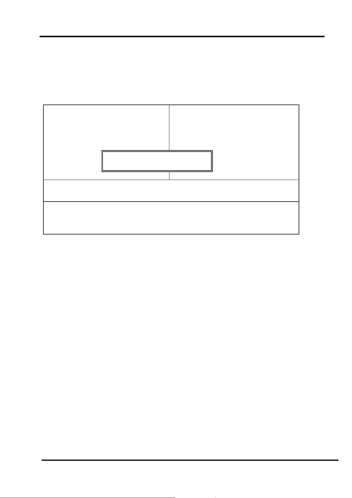
3.12 Save & Exit Setup
Select this option and press the <Enter> key to save the new setting information in the CMOS memory
and continue with the booting process.
Phoenix – Award BIOS CMOS Setup Utility
!Standard CMOS Features
!Advanced BIOS Features
!Advanced Chipset Features
!Integrated Peripherals
!Power Management
SAVE to C MO S and EX IT (Y/N)? Y
!PnP / PCI Configure
ESC: Quit # $ % : Select Item
F10: Save & Exit Setup
Save Data to CMOS
!PC Health Status
Load Optimized Defaults
Set Supervisor Password
Set User Password
setup
Saving
52
User’s Manual
Page 57
Chapter 3 BIOS Setup
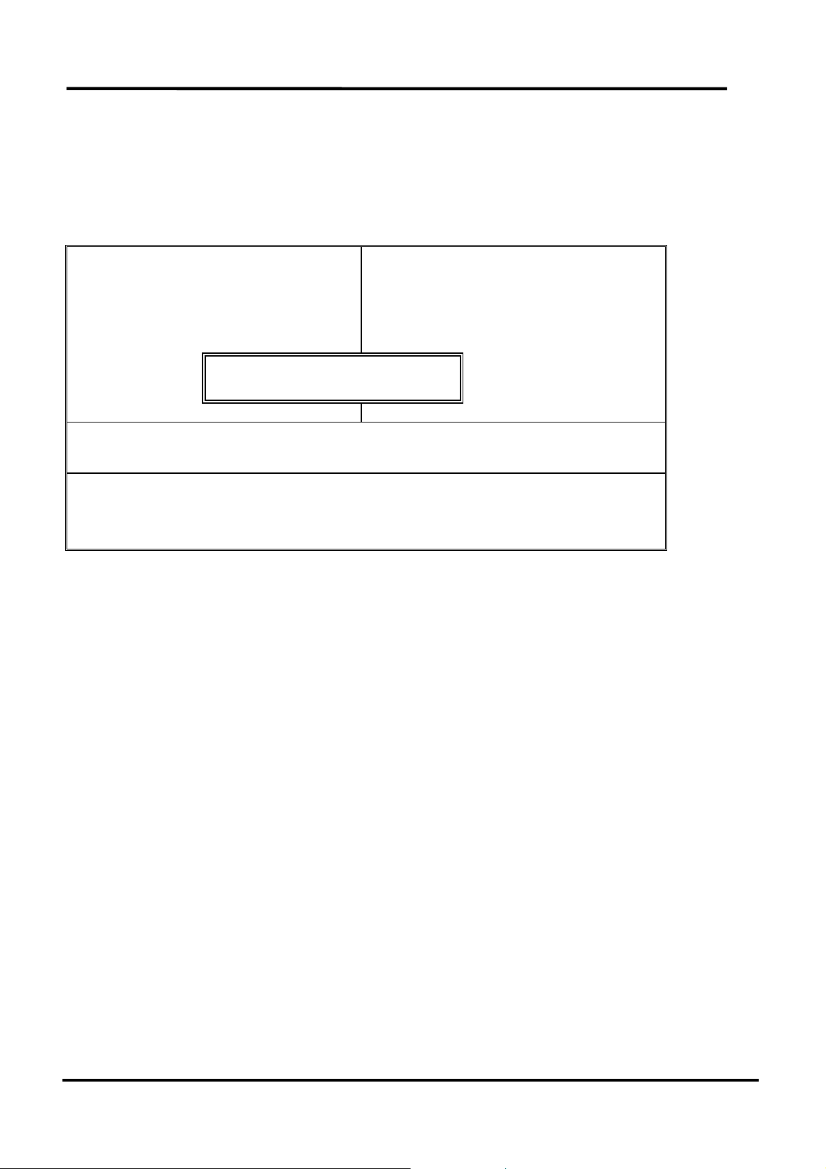
3.13 Exit Without Saving
Select this option and press the <Enter > key to exit the Setup Utility without recording any new values or
changing old ones.
Phoenix – Award BIOS CMOS Setup Utility
!Standard CMOS Features
!Advanced BIOS Features
!Advanced Chipset Features
!Integrated Peripherals
!Power Management
Quit Without Saving (Y/N)? N
!PnP / PCI Configure
ESC: Quit # $ % : Select Item
F10: Save & Exit Setup
Abandon all Data
!PC Health Status
Load Optimized Defaults
Set Supervisor Password
Set User Password
setup
Saving
User’s Manual
53
Page 58
Chapter 4. Drivers Support
Chapter 4 Drivers Support
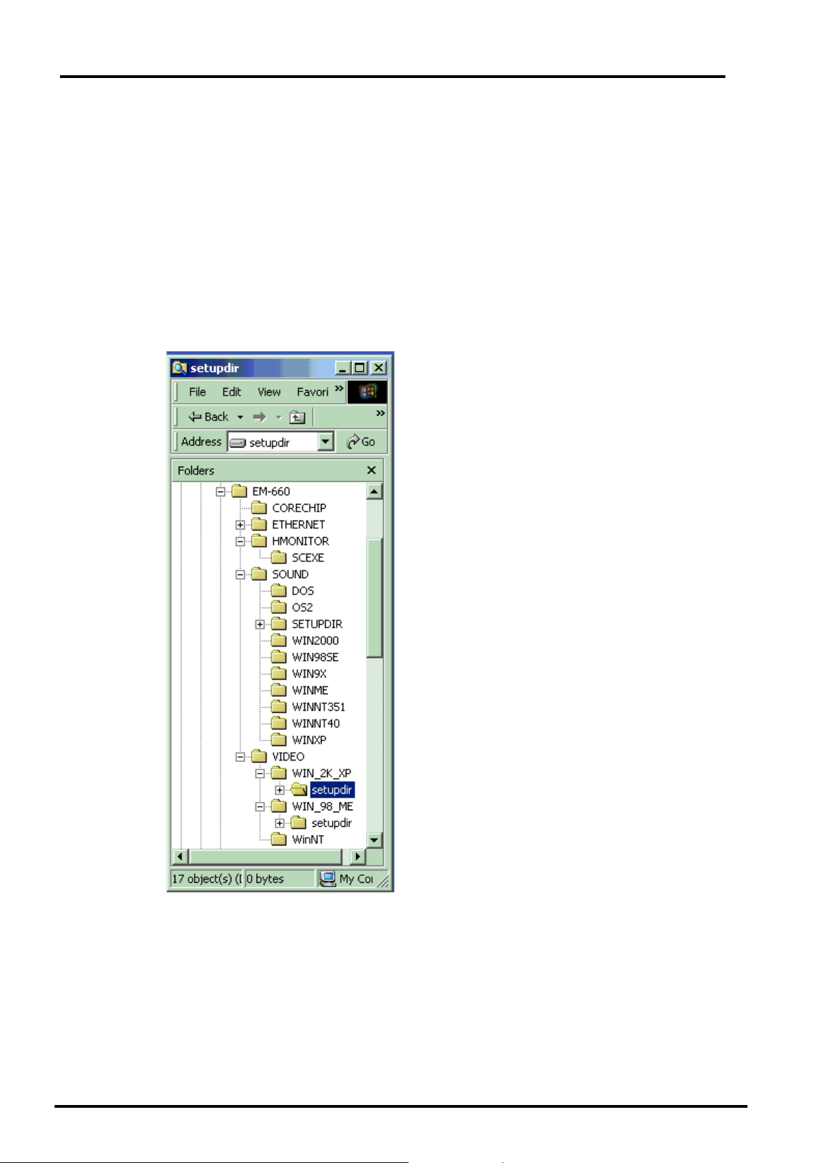
4.1 Use Your Driver CD-ROM
This chapter provides information on how to install the drivers in generally and related directory that come with
the CD-ROM in the package. Please follow the instructions set forth on the screen carefully.
1. Find the directory for your O/S accordingly.
2. Always read the README.TXT before installation
3. Run the *.EXE and follow the installation prompt step by step.
4.2 File Directory
Note: Windows Windows XP and ME should optimally configure the VIA chipset. Not need to run VIA Chipset
Software Installation Utility.
54
User’s Manual
Page 59

APPENDIXA. Watch-Dog Ti mer
To use the watch-dog timer:
Step 1. Enable and re-trigger the Watchdog timer: Output port 443H
Step 2. Disable : Output port 441H
EX.1: For DOS
Execute the DEBUG.EXE file under DOS, Then key-in O443. The system will reboot
automatically according to the time-out you set.
Enable Disable
C:\DOS> DEBUG C:\DOS> DEBUG
O 443 0~F O 441 0~F
EX.2: For assemble Language
Enable:
:
:
MOV DX, 443H
OUT DX, AL
:
:
Disable:
:
:
MOV DX, 441H
OUT DX, AL
:
Appendix A How to use watch-dog timer
APPENDIXB. Brightness Control
Under Command:
RUN EM60LAWD.EXE
EM-660 LCD Panel Brilight Control . For AWD BIOS.
VT686B GP04 (push up) ……. Press +
VT686B GP05 (push down) ….. Press-
Please input (+ / - /other key to exit )
User’s Manual
55
Page 60

Terms and Conditions
Date: 2003.02.27
Warranty Policy
1. All products are warranted against defe cts in materials and workmanship on a period of two years from the
date of purchase by the customer.
2. The buyer will bear the return freight charges for goods that are returned for repair within the warranty
period whereas manufacturer will bear the other way after repair.
3. The buyer will pay for repair (for the replaced materials plus service time) and transportation charges (both
ways) for items after the expiration of the warranty period.
4. If the RMA Service Request Form does not meet the stated requirement as listed on “RMA Service”, RMA
goods will be returned at the customer expense.
5. The following conditions are excluded from this warranty
A. Improper or inadequate maintenance by the customer.
B. Unauthorized modification or misuse.
C. Operation outside of the environmental specifications for the product.
:
RMA Service
1. Request a RMA#:
Complete and fax to Supplier the “RMA Request Form” to obtain a RMA number.
2. Shipping:
A. The customer is requested to fill up t he problem code as listed. If none of the code is selected,
please write the symptom description on the remark.
B. Ship the defective units with freight prepaid.
C. Mark the RMA # clearly on the box.
D. Shipping damage as a result of inadequate packing is the customer‘s responsibility.
E. Use the original packing materials whenever possible.
3. All RMA# are valid for 30 days only:
When RMA goods are received after valid RMA# period, the goods will be rejected.
Page 61

RMA Service Request Form
When requesting RMA service, please fill out this “RMA Service Request Form”.
Without this form your RMA will be REJECTED!!!
RMA No:
Company: Contact Person:
Phone No. Purchased Date:
Fax No.: Applied Date:
Return Shipping Address:
Shipping by:
Item Model Name Serial Number Configuration
Item Problem Code Failure Status
Air Freight □ Sea □ Express : □ Others:
□
Reasons to Return:
Purpose
Repair(Please include failure details) □ Tes ti ng
□
*Problem Code:
01:D.O.A.
02: Second Time R.M.A.
03: CMOS Data Lost
04: FDC Fail
05: HDC Fail
06: Bad Slot
07: BIOS Problem
08: Keyboard Controller Fail
09: Cache RMA Problem
10: Memory Socket Bad
11: Hang Up Software
12: Out Look Damage
Request Party
Authorized Signatures / Date Authorized Signatures / Date
13: SCSI
14: LPT Port
15: PS2
16: LAN
17: COM Port
18: Watchdog Timer
Confirmed By Supplier
19: DIO
20: Buzzer
21: Shut Down
22: Panel Fa il
23: CRT Fail
24: Others (Pls specify)
 Loading...