

Page 1

EM - 563 Series
5.25” EMBEDDED SBC
WITH VGA & FOUR 10/100MBPS LAN
FOR SOCKET370 PENTIUM III PROCESSOR
USER'S MANUAL
Page 2

COPYRIGHT©
This document is a copyright of the original manufacturer, 2002. The original manufacturer reserves
the rights to make improvement and/or modification to the product described in this manual at any
time wi thout further notice . T his manual ma y not, in whole or in part, be photocop ied, reproduced,
transcribed, translated, or transmitted in whatever form without the written consent of the
manufacturer, except for copies retained by the purchaser for backup purposes. All rights are
reserved.
TRADEMARKS
The following are trad emarks o r registered trademark s of their respectiv e companies: IB M, Intel, A MD,
Cyrix, NS, Award, AMI, Microsoft, Windows, Windows NT, Novell, SCO, PC/104, PICMG, ALI, UMC, SMC
and Winbond. Products mentioned in this manual are mentioned for identification purposes only. All
names of products or servic es appearing in this m anual are t he trad emarks or registered trademarks of
their respective organizations an d companies.
Copyright 2002
Version: 1.0
Date :2002/1/25
Page 3

TABLE OF CONTENTS
Chap ter 1 Introduction ........................................................................................................................... 1
1.1 Introduction........................................................................................................................................1
1.2 Features.............................................................................................................................................1
1.3 Specification.............................................................................................................. .........................2
1.4 Unpack your EM-563 ...........................................................................................................................2
1.5 Board Layout ......................................................................................................................................3
Chap ter 2 Insta l lation ............................................................................................................................. 4
2.1 Hardware Setup and Installation..........................................................................................................4
2.1.1 CPU Installation and Upgrading......................................................................................................4
2.1.2 System Memory Installation...........................................................................................................5
2.1.3 DiskOnChip Installation..................................................................................................................6
2.2 Jumper Settings and Connectors..........................................................................................................7
2.2.1 Board Outline................................................................................................................................7
2.2.2 Jumper Settings Summary.............................................................................................................8
2.2.3 I/O Connectors Summary ............................................................................................................10
Chap ter 3 BIOS Setup ...........................................................................................................................19
3.1 Running AMI BIOS ............................................................................................................................19
3.2 AMI BIOS HIFLEX Setup Utility...........................................................................................................20
3.3 Standard CMOS Setup .......................................................................................................................22
3.4 Advanced CMOS Setup ......................................................................................................................23
3.5 Advanced Chipset Setup ....................................................................................................................26
3.6 Power Management Setup .................................................................................................................29
3.7 PCI Plug and Play Setup.....................................................................................................................30
3.8 Peripheral Setup................................................................................................................................31
3.9 Hardware Monitor Setup....................................................................................................................34
3.10 Utility..............................................................................................................................................34
3.11 BIOS Defaults..................................................................................................................................34
Chap ter 4 Drivers S up port....................................................................................................................35
4.1 Use Your Driver CD-ROM ...................................................................................................................35
4.2 File Directory.....................................................................................................................................35
APPENDIX A. How to use watch-dog time r .........................................................................................36
RMA Servic e Request Form
Page 4

Page 5

Chapter 1 Introduction
Chapter 1 Introduction
1.1 Introduction
The new EM-563 Series embedded SBC is highly configurable with multiple features to suit different types of
comm ercial and industrial needs. Three Ethernet capability o f the EM-563 Series gives network administrators
another to o l to d eal with to day's chang in g ap plication needs. The board comes with the top-of-the-line Intel
82559 LAN chips could act as a firewall that sits between the Internet and a company's internal network. This
applies to Web (HTTP) servers, FTP servers, SMTP (E-mail) servers or DNS servers. The EM-563 can also be
used as an inter-network gateway that connects a number of local networks. Once again, the three Ethernet
capability and processin g power of the EM -563 Series gives it the ability to perform t hese fun ctions.
The new EM-563 Series is enhanced with Intel815E chipset; one 168-DIMM socket support up to 100/133
MHz SDRAM and one DiskOnChip f r om M-System socket support up to 288M B flash memory disk which provide
full func tionality and performance to be used "exactly" where you need it as well. EM-563 also features high
performance VGA display that support resolutions and color depths up to 1600x1200 x256 color at 85Hz.
EM-563 h as many expansion fun c tion suc h as one PCI expansion connector with one PCI riser card; on e F DD
interface support up to two floppy devices ; two IDE ports that support up to four IDE devices and Ultra
AT A/100/66/33 interface helps designers and integrators improve system performance by retrieving and sending
data faster. Everything you could need is on-board.
In addition, it is equipped with two RS-232 serial ports; four USB por ts; on e multi-mode parallel port which
supports SPP, E CP and E PP modes. It provides more flexible functions to satisfy all users' different application
requirements.
The EM-563 also offers several industrial features such as a 16 -level watchdog time-out intervals and contains
the h ealt h monitor ing hard ware. The healt h monitor i ng IC k eeps an eye on the CPU an d releases an audio
alarm when detecting abnormal operatin g voltage & t em perature o r malfunction of t he cooling fans. A nd with
its industrial grade reliability, the EM- 563 c an operate continuously at temperatures up to 60° C (140° F). All
these numerou s features provide an ideal price/p erformance solutio n for c ommercial and industrial applications
where stability and reliability are essential.
1.2 Features
Supports Socket 370 Celeron/Intel® Pentium III Processor, 133MHz FSB
Intel®815E chipset
Built–in four 10/100BASE- TX Ports with RJ - 45 connectors
Socket for DiskOnChip
With one PCI expansion slot
4 USB ports and supports 4 Ultra ATA 100 devices
5.25” Form Facto r, special design for firewall an d network applications
1 User’s Manual
Page 6

Chapter 1 Introduction
1.3 Specification
EM-563 Series
Processor
Chipset
System Memory / RAM One 168-pin DI MM sockets, support 100/133 MHz SDRAM and up to
BIOS
Flash Memory Disk Reserved socket for DiskOnChip from M-System, support up to 288 MB
Gra phics C ontroller Int ern al graphi c c o ntrol l er wi th In t el ’s Dy n am i c Video Memory
Network Interface Three Intel 82559 chip, support three-10/100 Base-TX Ethernet, three
IDE Drive Interface Two PCI IDE ports that support up to four IDE devices and Ultra
Fl oppy Drive Interface One FDD port, support up to two floppy devices
Serial Port Two COM ports, one RS-232 DB-9 connector and one RS-232 2x5x2.54
Parallel Port One multi-mode parallel port ( SPP / EPP / EC P )
Bus Interface PCI bus slot
RTC Internal RTC with Li battery
Keyboard/Mouse 6-pin keyboard/mouse pin header
Watchdog Timer 16-level time-out intervals
Universal Serial Bus Support 4 USB ports (4x5 pin headers)
Health Monitoring Enhanced hardware monitor functions with optical sensor
Operat ing Temperature
St o r age Temperature
Humidity
Dimensions
EMI/EMS EN 50081-1/1994>EN 55022/1997>EN 61000- 3- 2/1995
Remark PCI Rev. 2.2 compliant
ORDERING INFORMATION
Intel Pentium III Coppermine / Celeron Processor in Socket
370(66/100/133 MHz) and up to 1GB
Intel 815E chipset
512 SDRAM
Award licensed BIOS
flash memory disk
Technology, resolution up to 1600 x 1200 x 256 colors @ 85 Hz, with
VGA 2x6x2.54 mm pin header with housing
RJ-45 external connecto rs with ACT LED, LNK LED
ATA/100/66/33
mm pin header with housing
0 °C~60 °C
-20 °C~70 °C
5 %~95% RH, non-condensing
203 x 146 x 25 mm ± 0.5 mm
>EN 61000-3-3/1995, EN 50082-1/1994>IEC 1000-4-2/1995,
IEC 1000-4-3/1995, IEC 1000-4-4/1995, EN55024
1.4 Unpack your EM-563
Befo re you beg in to install yo ur card , please make su re that you received th e following m at erials as listed
below:
EM-563 x 1 pc 5.25" Embedded Single Board Computer
FDD Cable x 1 pc 34 to 34 - pin Standard Header Flat Ribbon Cable
IDE Cable x 1 pc 40-pin IDE Cable
VGA Cable x 1 pc 12- pin Standard Header to 15-pin/3- Row D-Sub Cable
Keyboard and Mouse Cable x 1 set 8-pin connector to PS/2 Keyboard and Mouse Cable
Driver Utility CD-ROM x 1 pc Drivers & Utilities
User's Manual x 1 pc This User's Manual
2 User’s Manual
Page 7

1.5 Board Layout
Chapter 1 Introduction
3 User’s Manual
Page 8
Chapter 2 Installation
Chapter 2 Installation
2.1 Hardware Setup and Installation
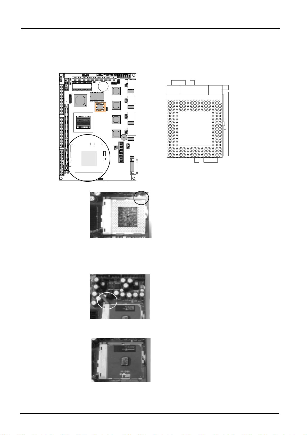
2.1.1 CPU Installation and Upgrading
PGA370
Step 1: Loc ate t he ZIF socket and open it by first pulling the lever of socket upward.
Step 2: In sert the CP U into the socket. Please keep the lever right an gle when inserting CPU.
Step 3: When inserting the CPU please note the correct orientation as shown. The notched corner should
point towar d the end of the lever.
Step 4: Pus h the lever d own to clo s e t he socket.
Step 5: Attach th e heatsink onto the CPU.
4 User’s Manual
Page 9
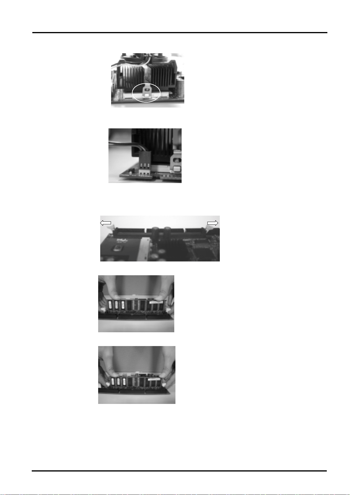
Step 6: Push the clip of heatsink downward to hock the ear of socket firmly.
Step 7:Finally , attac h the fan cable to the C P U fan header.
2.1.2 Sy stem Memory Installation
Step 1:O p en latches of DIMM socket.
Chapter 2 Installation
Step 2:Insert the R A M module into the DI MM socket.
Step 3:P ress the latches into th e n o tches of the R A M module.
5 User’s Manual
Page 10
Chapter 2 Installation
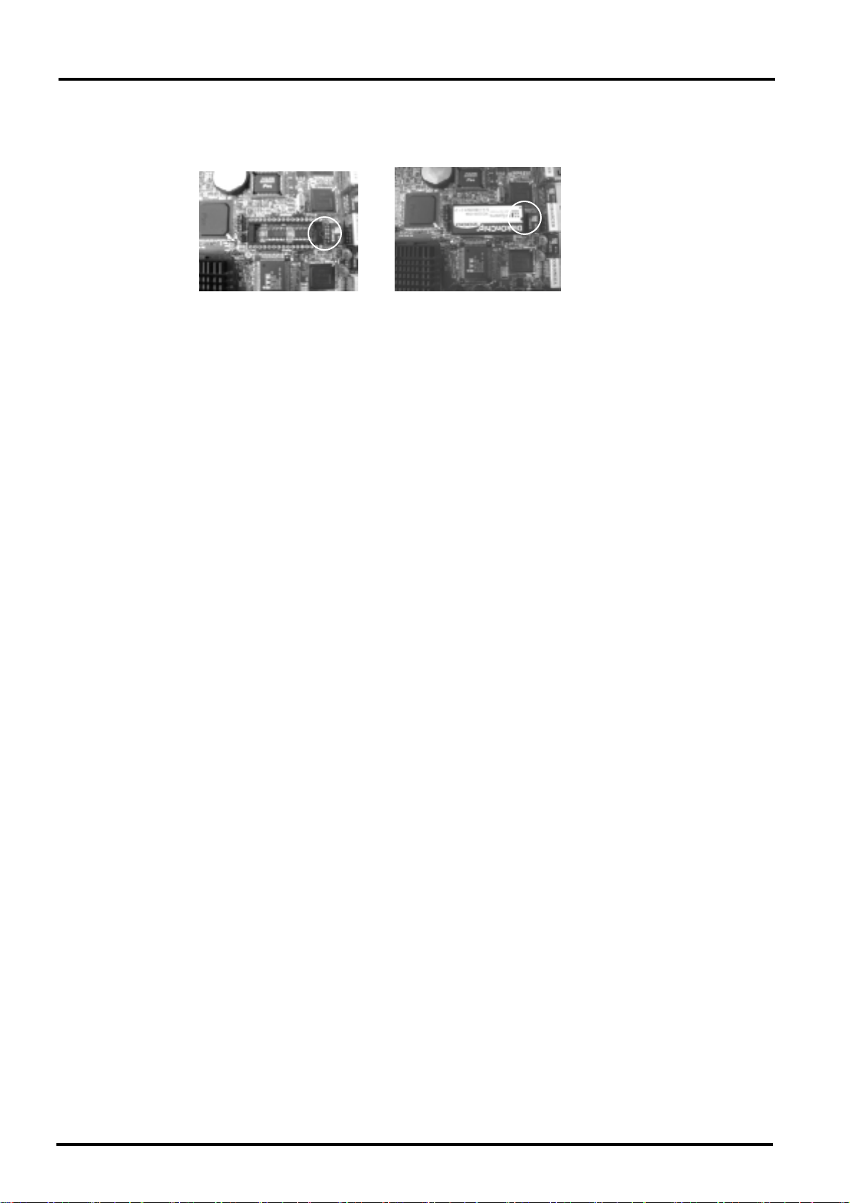
2.1.3 DiskOnChip Installation
Please mak e sure the central polarization key on the socket, and place the DiskOnChip as t he same direction.
6 User’s Manual
Page 11
3
A
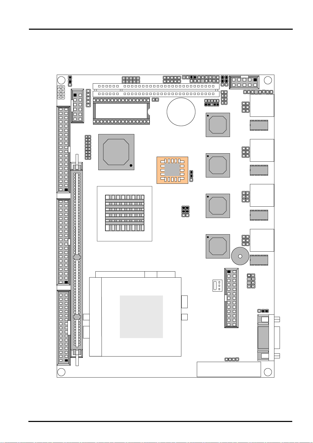
2.2 Jumper Settings and Connectors
2.2.1 Board Outline
DIA1
1
7
IDEB2
1
3
2
8
CMOS1
1 2
IRDA1
1
5
VGAB1
16 15
SM1
2 1
IDEB1
DIMMA1
USBA1 USBA2
2
1
10
9
DOC1
Chapter 2 Installation
JFA5
JFA6
PLRS1
ISP2
10
2
1
2 1 2
1
10
8
9
PSW1
10
1
9
SDOC1
COMB1
1 1 1
9
1 2
DOA1
1
2
LEDB1
8 7
LEDB2 LEDB3
6 5
1 2
ISP1
1 8
LANB1
LANB2
LEDB4
5 6
1 2
5 6
1 2
5
6
LANB3
LANB4
1 2
5 6
JFA7
1
JFA4
3
FDCA1
CPU
FAN1
1
LPTA1
ATXC1
4
PS1
1
PKM1
KBPW1
3
1
COM
1
7 User’s Manual
Page 12
Chapter 2 Installation
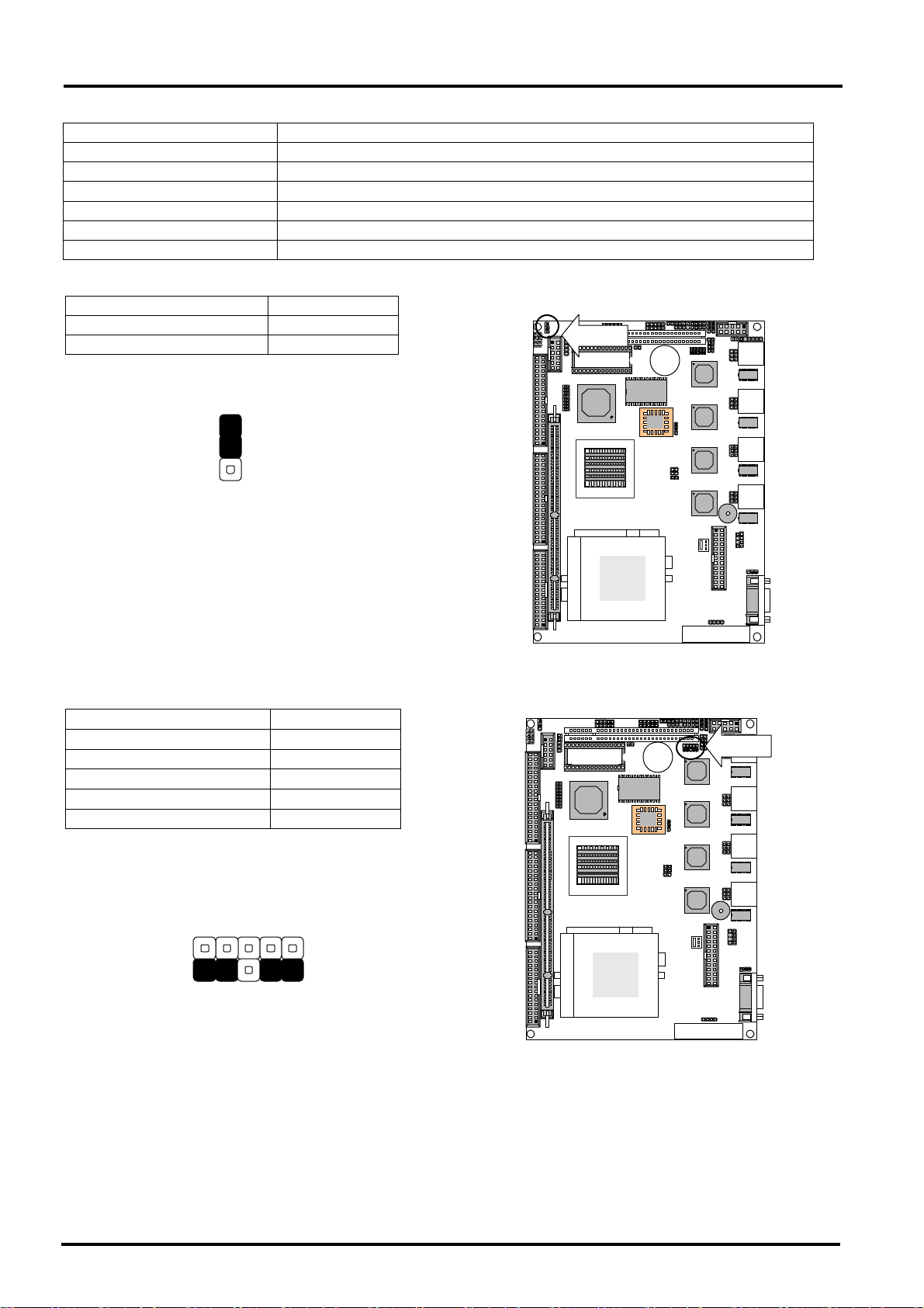
2.2.2 Jumper Settings Summary
LOCATION FUNCTION
CMOS1 Clear CMOS Data
SDOC1 Select Flash Disk Address
KBPW1 PS/2 Keyboard & Mouse
JFA4 BIOS Locked
JFA7 5Vsb Select
JFA5/JFA6 Manufacturer Default
CMOS1 : Clear CM OS Data
Description CMOS1
Normal (Default) 1-2
Clear CMOS 2-3
COMS1
CMOS1
1
2
3
S D OC1 : Select Fl ash Disk Address
Flash Disk A ddress Sd oc1
CC00H~CDFFH 1-2,9-10
D000H~D1FFH 3-4,7-8
D400h~D5FFH 3-4,9-10
D800H~D9FFH 5-6,7-8
DC00H~DDFFH 5-6,9-10
10
9
SDOC1
1
2
SDOC1
8 User’s Manual
Page 13
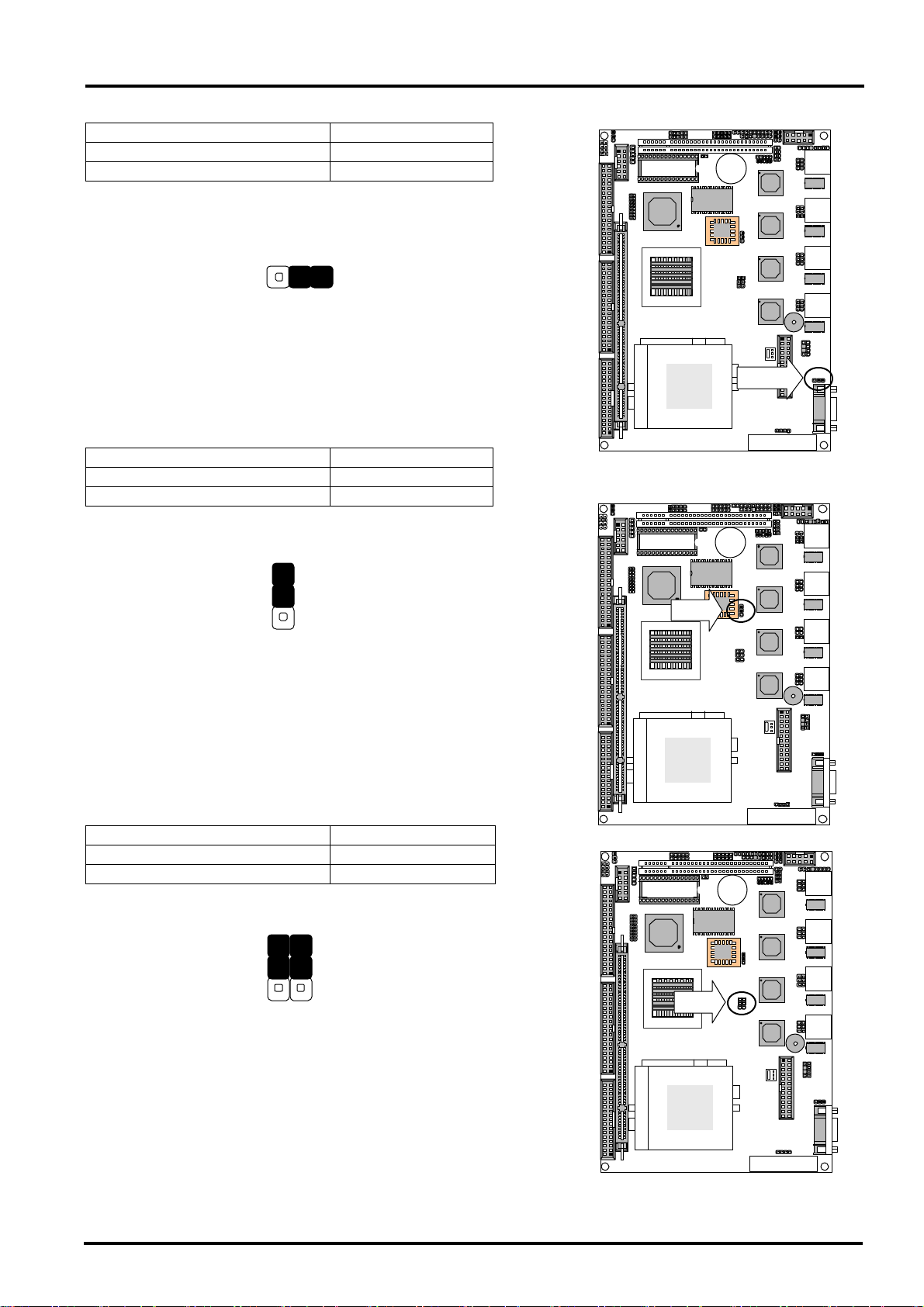
KB PW1 : PS/ 2 Keyboard & Mouse
PS/2 Keyboard/Mouse KBPW1
+5V (Defau lt) 1-2
+5V STANDBY 2-3
KBPW1
3
1
JFA 4 : BIOS Locked
Description JFA4
UnlockedDefault) 1-2
Locked 2-3
JFA4
1
3
JFA7 : 5VSB Select
Description JFA7
VCC(Default) 1-3,2-4
STB5V 4-6,3-5
JFA7
1
2
5
6
JFA5/JFA6 : Manufacturer Default(1-2)
Chapter 2 Installation
KBPW1
JFA4
JFA7
9 User’s Manual
Page 14
Chapter 2 Installation
2.2.3 I/ O Connectors Summary
LOCATION FUNCTION
LPTA1 Parallel Connector
FAN1 FAN Connector
IDEB1/2 IDE Interface Connector
FDCA1 Floppy Interface Connector
VGAB1 External VGA Connector
LANB1/2/3/4 LAN Connector
COMA1 RS-232 Serial Port#1 Connector
COMB1 RS-232 Serial Port#2 Connector
IRDA1 Alternate IrDA
USBA1/2 U S B Por t #1 & #2 Connector
PKM1 PS/2 Keyboard & Mouse Connector
PLRS1 Power LED,HD LED, Reset, Speaker Connector
DOC1 Disk-On C hip Sock et
PSW1 ATX Power Button
ATXC1 ATX Function
LEDB1/2/3/4 Extension LAN Status LED
DIA1 Digital Input P o rts
DOA1 Digital Output Ports
SM1 AC97 Codec and KB/MS with daughter board
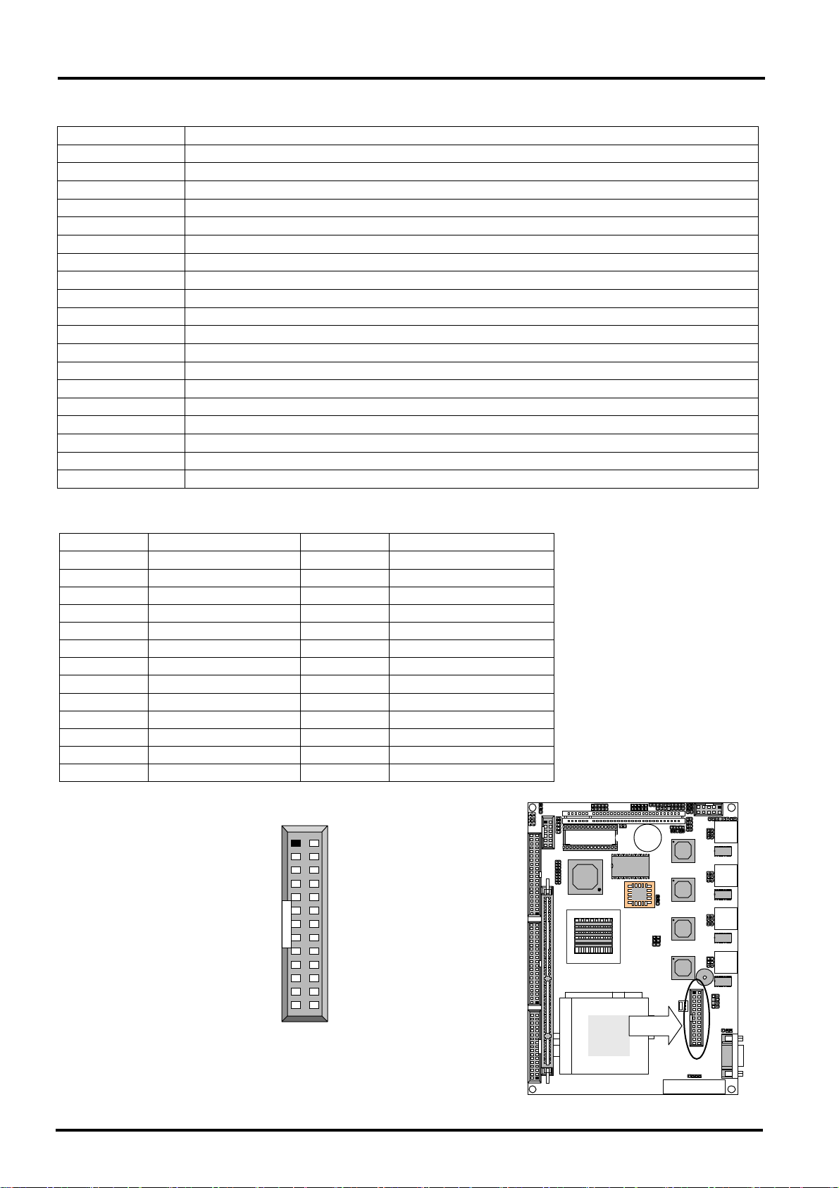
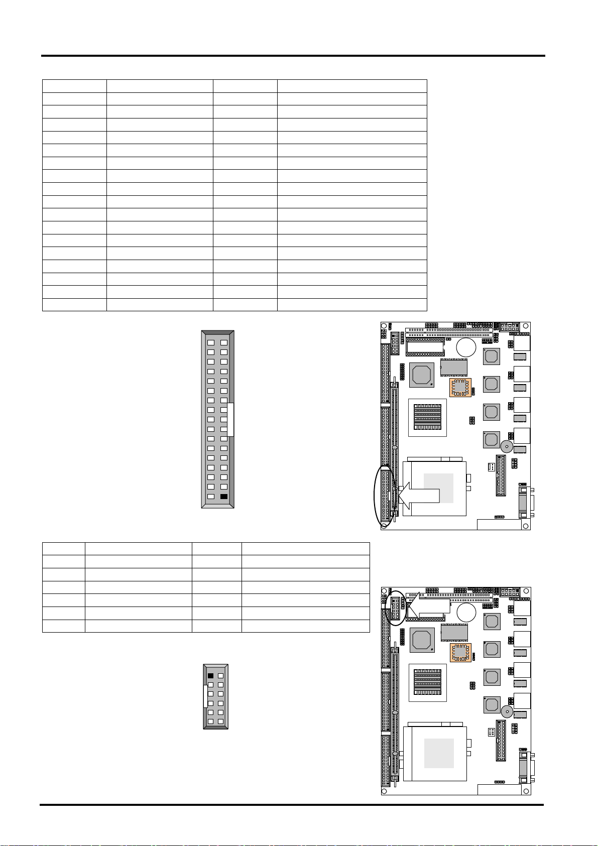
LPTA1 : Parallel Connector (26 Pin 2.54mm Pitch Header )
Pin No. Description Pin No. Description
1 Strobe # 2 Auto Form Feed
3 Data0 4 Error #
5 Data1 6 Initialize #
7 Data2 8 Printer Select IN #
9 Data3 10 Ground
11 Data4 12 Ground
13 Data5 14 Ground
15 Data6 16 Ground
17 Data7 18 Ground
19 Acknowledge # 20 Ground
21 Busy 22 Ground
23 Paper Empty 24 Ground
25 Printer Select 26 NC
LPTA1
1
2
25
10 User’s Manual
26
LPTA1
Page 15
1
2
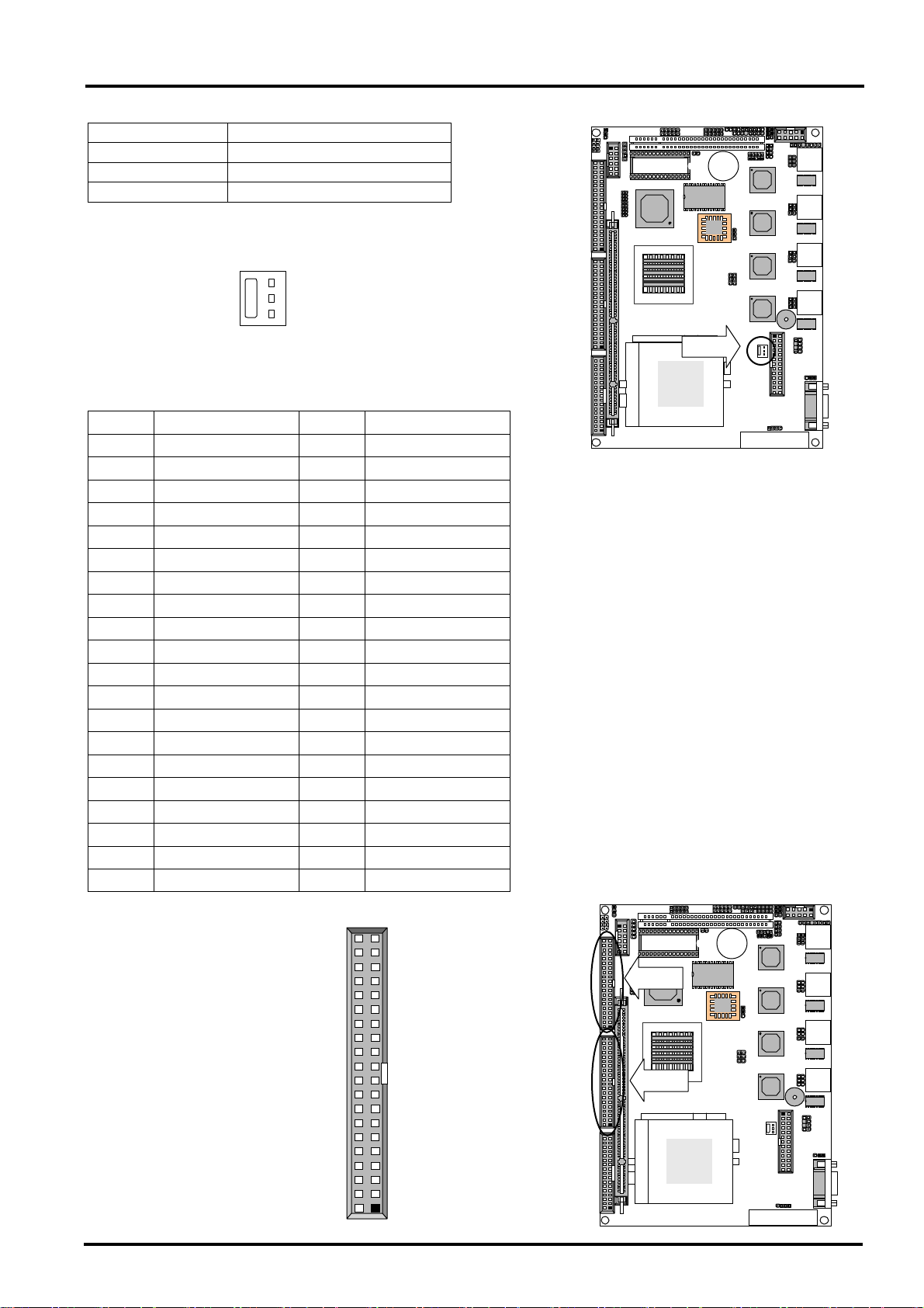
FAN1 : FAN Connector
Pin No. Description
1 Ground
2 +12V
3 FAN Status
FAN1
1
3
IDEB1
IDEB2 : IDE Interface Connector
、
、
、
、
Pin No. Description Pin No. Description
1 Reset # 2 Ground
3 Data 7 4 Data 8
5 Data 6 6 Data 9
7 Data 5 8 Data 10
9 Data 4 10 Data 11
11 Data 3 12 Data 12
13 Data 2 14 Data 13
15 Data 1 16 Data 14
17 Data 0 18 Data 15
19 Ground 20 NC
21 DMA REQ# 22 Ground
23 IOW # 24 Ground
25 IOR # 26 Ground
27 IOCHRDY 28 Ground
29 DMA ACK # 30 Gr oun d
31 Interrupt 32 NC
33 SA1 34 PD80P / SD80P
35 SA0 36 SA2
37 HDC CS0 # 38 HDC CS1 #
39 HDD Active LED # 40 Ground
Chapter 2 Installation
FAN1
IDEB1/2
40
39
IDEB2
IDEB1
11 User’s Manual
Page 16
Chapter 2 Installation
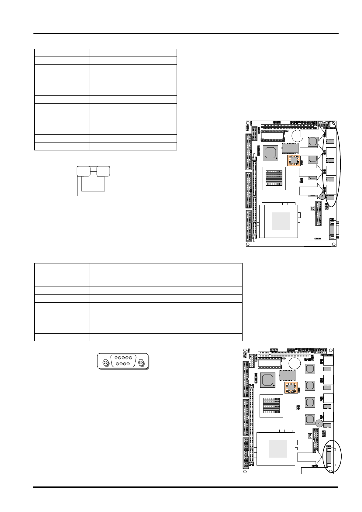
FDCA1 : Floppy Interface Connector
Pin No. Description Pin No. Description
1 Ground 2 Density Select
3 Ground 4 NC
5 Ground 6 DS1
7 Ground 8 Index #
9 Grou n d 10 Motor Enable A #
11 Ground 12 Drive Select B #
13 Ground 14 Drive Select A #
15 Ground 16 Motor Enable B #
17 Ground 18 Direction #
19 Ground 20 Step #
21 Ground 22 Write Data #
23 Ground 24 Write Gate #
25 Ground 26 Track 0 #
27 Ground 28 Write Protect #
29 NC 30 Read Data #
31 Ground 32 Head Side Select #
33 NC 34 Disk Change #
FDCA1
34
33
2
1
VGAB1 : External VGA Connector
Pin No. Description Pin No. Description
1 R 2 Ground
3 G 4 Ground
5 B 6 Ground
7 H-SYNC 8 Ground
9 V-SYNC 10 Ground
11 Detect-display Data 12 Deteck-display CLOCK
VGAB1
1
2
11
12
FDCA1
VGAB1
12 User’s Manual
Page 17
4
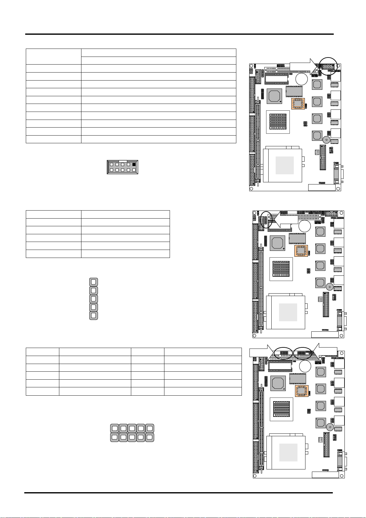
LANB1
LANB2
、
、
、
、
LANB3
、
、
、
、
Pin No. Description
1 TX+
2 TX3 RX+
4 T45
5 T45
6 RX7 T78
8 T78
9 Link10 Link+
11 ACT12 ACT+
LANB1/2/3/4
LANB 4 : LAN Connector ( RJ-45 with LED )
、
、
、
、
Chapter 2 Installation
LANB1
LANB2
LANB3
LANB
COMA1 : RS-232 Serial Port #1 Connector ( D-Sub )
Pin No. Description
1 Data Carrier Detect ( DCDA # )
2 Receive Data ( RXDA )
3 Transmit Data ( T XDA )
4 Data T erminal Read y ( DTRA # )
5 Ground ( GND )
6 Data Set Ready ( DSRA # )
7 Request To Send ( RTSA # )
8 Clear To Send ( CTSA # )
9 Ring Indicator ( RIA # )
1 5
COMA1
9 6
COMA1
13 User’s Manual
Page 18
Chapter 2 Installation
2
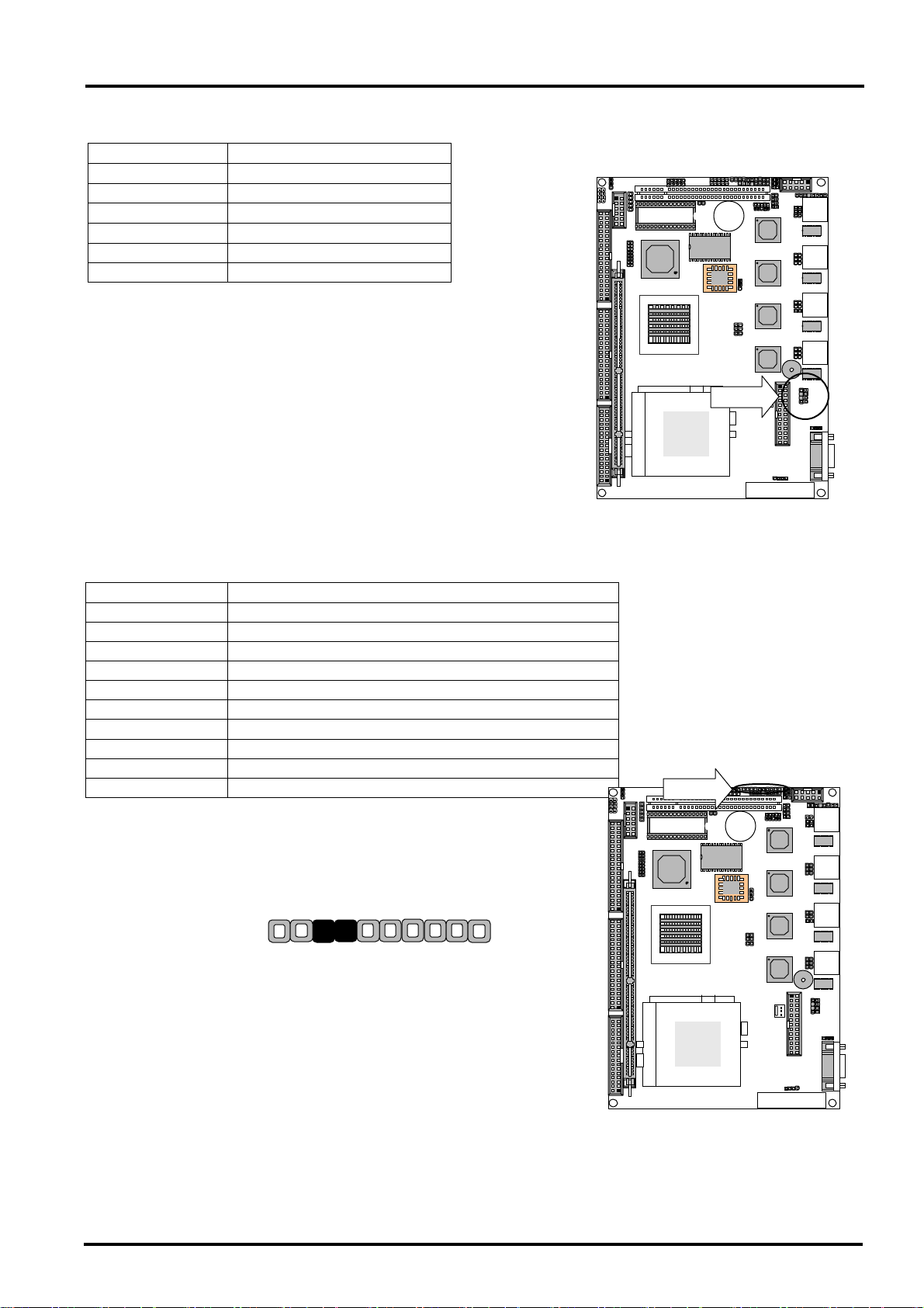
COMB1 : RS-232 Serial Port #2 Connec tor ( Header )
Pin No.
Description
RS-232
1 Data Carrier Detect (DCDB #)
2 Data Set Ready (DSRB #)
3 Receive Data (RXDB)
4 Request T o S end (RTSB #)
5 Transmit Data (TXDB)
6 Clear To Send (CTSB #)
7 Data Terminal Read y (DTRB #)
8 Ring Indicator (RIB #)
9 Ground
10 NC
9
10
COMB1
1
2
IRDA1 : Alternate IRDA
Pin No. Description
1 +5V
2 NC
3 IRRX
4 GND
5 IRTX
IRDA1
1
5
USBA1
USBA2:USB Port #1 & #2 Connector 2x5 Pin 2.54mm
、
、
、
、
Pin No. Description Pin No. Description
1 USB_VCC 2 USB_VCC
3 USB D- 4 USB D05 USB D+ 6 USB D0+
7 Ground 8 Ground
9 USB Port#2Ground 10 USB Port#1 Ground
USBA1
COMB1
IRDA1
USBA
USBA1/2
2
1
14 User’s Manual
10
9
Page 19
PKM1 : PS/2 Keyboard & Mouse Connector
Pin No. Description
1 PS/2 Keyboard Data
2 PS/2 Mouse Data
3 Ground
4 +5V
5 PS/2 Keyboard Clock
6 PS/2 Mouse Clock
Chapter 2 Installation
PLRS 1 : Power LED,HD LED,Reset, Speaker Connector
Pin No. Description
1 Power LED +
2 GND
3 HDD LED +
4 HDD LED -
5 RESET SW +
6 RESET SW – (GND)
7 External Speaker -
8 Internal Buzzer -
9 NC
10 External Speaker+
PLRS1
1 10
PKM1
PLRS1
15 User’s Manual
Page 20
Chapter 2 Installation
1
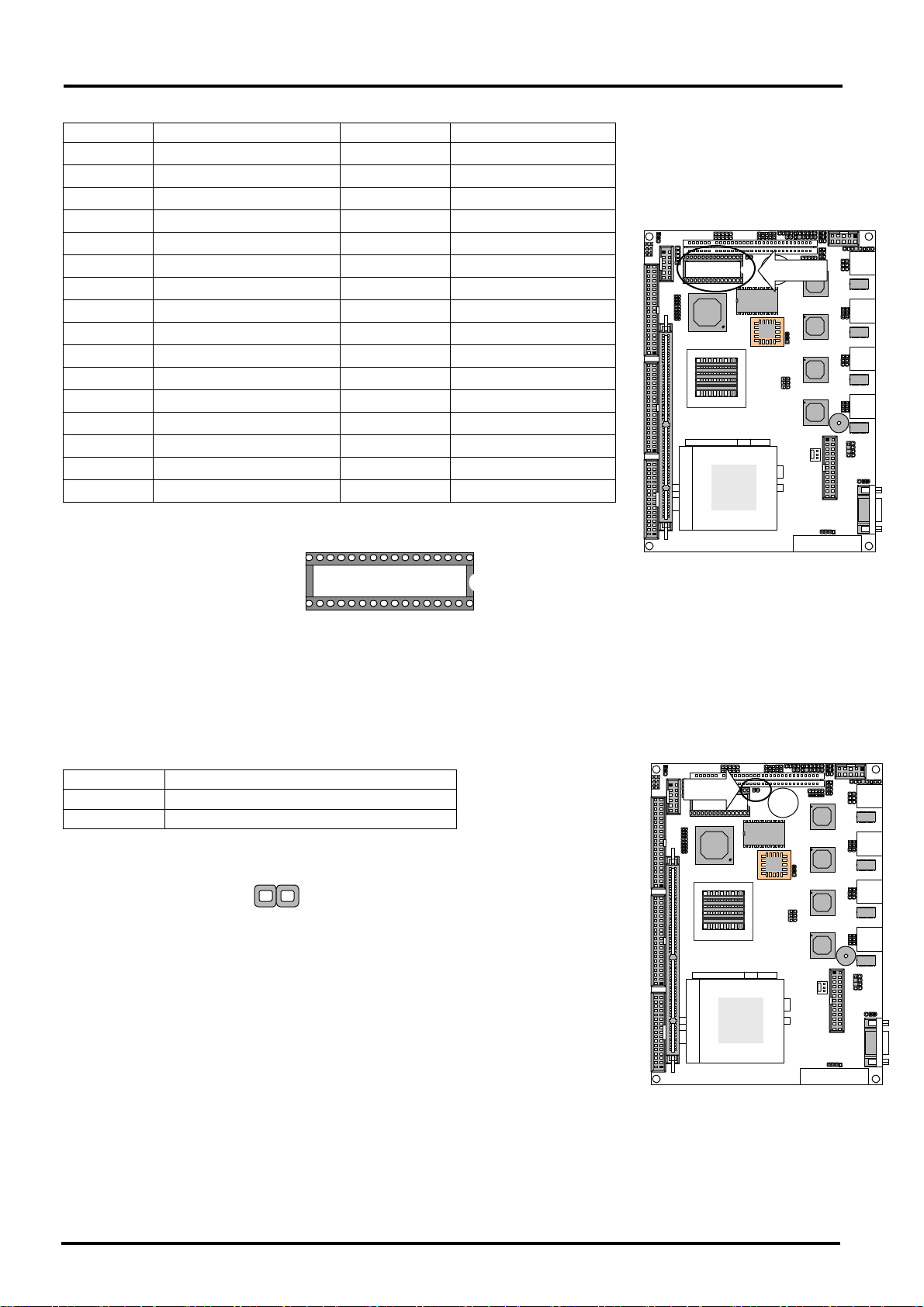
DOC1 : Disk-On-Chip Socket
Pin No. Description Pin No. Description
1 AEN 17 SD3
2 IOW# 18 SD4
3 SA15 19 SD5
4 SA12 20 SD6
5 SA7
21 SD7
6 SA6 22 CE#
7 SA5 23 SA10
8 SA4 24 SMEMR#
9 SA3 25 SA11
10 SA2 26 SA9
11 SA1 27 SA8
12 SA0 28 SA13
13 SD0 29 SA14
14 SD1 30 +5V
15 SD2 31 SMEMW#
16 GND 32 +5V
DOC1
17
DOC1
16
PSW1: ATX Power Button
Pin No. Description
1 PANSW
2 GND
PSW1
2
1
32
PSW1
16 User’s Manual
Page 21
A
A
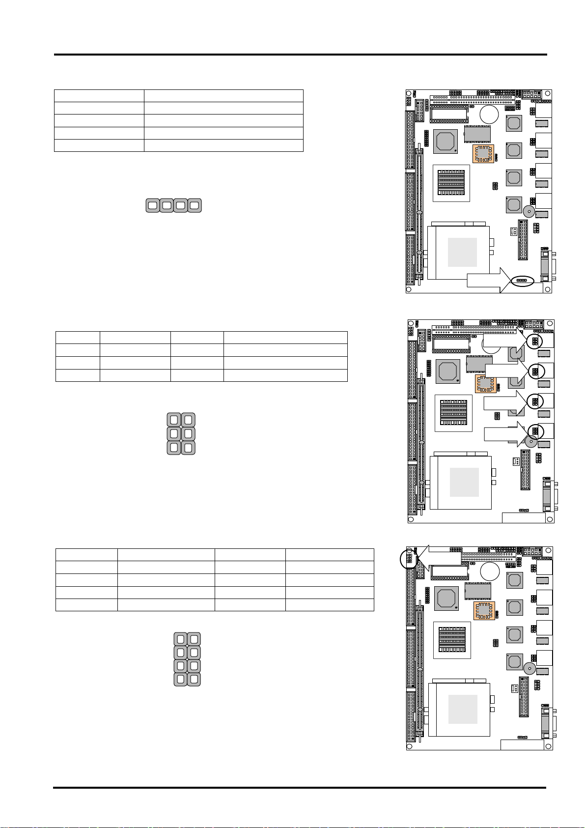
ATXC1: ATX Function
Pin No. Description
1 GND
2 +5V STANDBY
3 GND
4 PSON
4
TXC1
1
LEDB1
LEDB2
、
、
、
、
LEDB3
、
、
、
、
LEDB 4: Extension LAN Status LED
、
、
、
、
Pin No. Descri ption Pin No. Description
1 10/100M- 2 10/100+
3 Link- 4 Link+
5 Active- 6 Active+
LEDB1/2/ 3/ 4
1
2
5
6
DIA1: Digital Input Ports
Pin No. Description Pin No. Description
1 GND 2 IN0
3 GND 4 IN1
5 GND 6 IN2
7 GND 8 IN3
DIA1
1
2
Chapter 2 Installation
TXC1
LEDB1
LEDB2
LEDB3
LEDB4
DIA1
7
8
17 User’s Manual
Page 22
Chapter 2 Installation
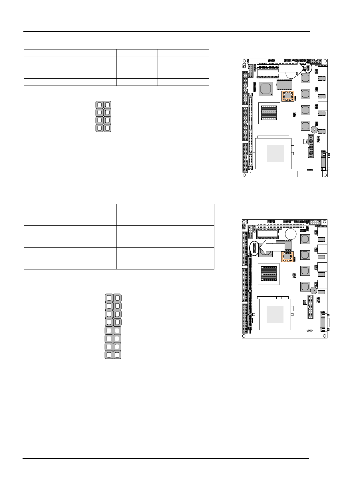
DOA1: Dig ital Outp ut Ports(2x4 Pin 2.54mm Header)
Pin No. Description Pin No. Description
1 OUT0 2 VCC
3 OUT1 4 VCC
5 OUT2 6 VCC
7 OUT3 8 VCC
DOA1
2 1
DOA1
7
8
SM1: AC97 Codec and KB/MS with daughter board
Pin No. Description Pin No. Description
1 ICH_SPKR 2 AC97
3 AC_RST- 4 VCC
5 SYNC 6 GND
7 SDINO 8 +3.3V
9 NC 10 GND
11 BITCLK 12 +5V STANDBY
13 SDOUT 14 NC
15 MSDAT 16 MSCLK
SM1
16 15
SM1
2
1
18 User’s Manual
Page 23

Chapter 3. BIOS Setup
Chapter 3 BIOS Setup
The AMI‘s ROM BIOS provides a built-in Setup program that allows user to modify the basic system
configuration and settings. The modified data will be stored in a battery-backed CMOS RAM so that these data
will be retained even when the power is turned off. In general, the information saved in the CMOS RAM stay
unchanged unless there is configuration change in the system, such as hard drive replacement or new
equipment is ins talled. AMI is a registered trademark of th e American Megatrends, In c.
3.1 Running AMI BIOS
The S etup Utility is stored in t he BIOS ROM. When th e power of t he compu t er system is turned on, a screen
messag e appears to g ive you an opportunity to call u p the Setup Utility; while t he BIOS w ill enter the Power O n
Self Test (P OST) rou t ines. The PO ST routin es perfor m various diagnostic checks w hile initializing the board
hardware. If the routines encounter an error d uring the tests, the error will be reported in either of the two
dif ferent way s – (1) hear a series of short b eeps, or (2 ) see an error message on the screen dis play . Th ere are
two kinds of error: fatal or non-fatal. The system can usually continue to boot up sequence with the non-fatal
errors. Non-fatal error messages usually appear on the screen along with the following instructions:
“ Press <F1> to RESUME ”
Writ e down the mes sage and press the F 1 key to continue the bootup s equence. After the POST r o utines are
completed, the following message appears:
“ Press DEL to enter SETU P ”
Entering Setup
Turn on the pow er of the computer system and press <Del> imm ediately. If y o u don’t have the ch ance to
respond, reset the system by simultaneously typing the <Ctrl>, <Alt> and <Delete> keys, or by pushing the
‘ Reset ’ button on th e system cabinet. You can also restart by tu rning the system O FF then ON.
Note: BIOS versions ar e regularly updated form time to time without notices. Theref o re, the options a v ailable in
your setup screen may differ fr om the options shown in this manual.
19 User’s Manual
Page 24

Chapter 3. BIOS Setup
3.2 AMI BIOS HIFLEX Setup Utility
To a ccess the AMI BIOS HIFLEX SETUP UTILITY program, press the <DEL> key. The screen display will
appears as:
Main Program Screen
AMIBIOS HIFLEX SETUP UTILITY
© 2001 American Megatrends, Inc . All Rights Reserved
Standard CMOS Setup
Advanced CMOS Setup
Advanced Chipset Setup
Power Management Setup
PCI / Plug and Play Setup
Peripheral Setup
Hardware Monitor Setup
Auto -Detect Hard Disks
Change User Password
Change Supervisor Password
Auto Co nfigur ation with Optimal Settings
Auto Configuration with Fail Safe Settings
Save Settings and Exit
Exit Witho ut Saving
Standard CMOS setup for changing time, date, hard disk type, etc.
ESC : Exit ↑↓ : Sel F2/F3 : Color F10 : Save & Exit
This s creen provides access to the utility‘s various functions.
Listed below are the explanation o f the keys displayed at the bottom of the screen:
<ESC> : Exit the utility.
: Use arrow keys to move cursor to your desired selection.
<F2 > / <F3> : Changes background and foreground colors.
<F10> : Saves all changes made to Setup and exits program.
Standard CMOS Setup: Use this menu for basic system configurations, such as time, date etc.
Advanced CMOS Setup: Use this menu to specify your settings for Advance CMOS.
Ad vanc ed Chi pse t Se tup : Use this menu to change the values in the chipset registers and optimize your
system’s perfor mance.
Power Management S etup: Use this menu to specify your settings for power management.
PCI / Plug and Play Setup: Use this menu to specify your settings for PCI/Plug and Play.
Peripheral Setup: Use this men u to specify yo u r settings for in teg rated peripherals.
Hardware Monitor Setup: This entry shows your PC’s current status, and allows you to adjust CPU clock,
core voltage etc.
20 User’s Manual
Page 25

Chapter 3. BIOS Setup
Auto-Detect Hard Disks: Use this menu to au to matic ally d etec t the characteristics o f most hard drives.
Change User Password: Use this menu to set U s er Password.
Change Supervisor Password: U s e this menu to set Sup er v is or Password.
Auto Con figu ration with Op timal Se ttings: This option allows you to load the default values to your
system configuration. These default settings are optimal and enable all high performance features.
Auto Configuration with Fail Safe Settings: This option allows y o u to load the troubleshooting default
values permanently stored in the BIOS ROM. These default settings are non-optimal and disable all
high-performance features.
Save Settings and Exit: Save changes to CMOS and exit setup.
Exit Without Saving: Abandon all changes and exit setup.
User’s Manual
21
Page 26

Chapter 3. BIOS Setup
3.3 Standard CMOS Setup
When you selec t t he “ST A NDARD CMOS SETUP” on the main program, t he screen display will appears as:
Standard CMOS Setup Screen
AMIBIOS SETUP – STANDARD CMOS SETUP
© 2001 American Megatrends, Inc . All Rights Reserved
Date (mm/dd/yyyy)
Time (hh/mm/ss)
Floppy Drive A :
Floppy Drive B :
LBA Blk PIO 32 Bit
Type Size Cyln Head WPcom Sec Mode Mode Mode Mode
Pri Master
Pri Slave
Sec Master
Sec Slave
: Auto
: Auto
: Auto
: Auto
Boot Sector Virus Protection Disabled
Month
Day
Year
: Jan
: 01
: 1980
Standard CMOS Setup options are displayed by choosing the Standard field from the AMIBIOS HIFLEX
SETUP menu. All Standard Setup options are described below.
Date: This all o ws you to set the system to the date that yo u w an t (usually the c urrent dat e). The format is
<day><month><date><year>.
Day Day of the week, f rom Sun to Sat, d eter min ed b y BIOS. Real-o nly.
Month The month from Jan. through Dec.
Date The date from 1 to 31 can be keyed by numeric function keys.
Year The year can be adjusted by users.
Time: This allows you to set the system time that you want (usually the curre nt time). The time format is
<hour><minute><second>.
Pri Master / Pri Sl a ve: Press PgUp/<+> or PgDn/<-> to se lect the hard disk drive ty pe. The specification
of hard disk drive will sho w up on the right han d accor ding to your selection.
Type Type of the device.
Size Capacity of the device.
Cyln Number of cylinders.
Head Number of heads.
Wpcom Write preco m pensation cylinder.
Sec Number of sectors.
Mode Access mode.
Floppy Drive A, B: Choo s e t he Floppy Drive A or B field to sp ecify t he floppy drive type. Th e setting s are
360 KB 51/4”, 1.2 MB 51/4”, 720 KB 31/2”, 1.44 MB 31/2”, or 2.88 MB 31/2”.
Boot Sector Virus Protection: The item is to set the Vir us Warning f eat ure f or IDE Hard Disk boo t sector
protection. When
Enabled
or the p ar tition tab le of the HDD is attempted. Setting options:
Note: This feature only protects the boot sector, not the whole hard disk.
: Wed J an 23, 2002
: 22:22:32
1.44 MB 31/
2
Base Memory
Extd Memory
: 639KB
: 254MB
Not Installed
Off
Off
Off
Off
- Dec
- 31
- 2099
ESC:Exit ↑↓ : Sel
PgUp/PgDn: Modify
F1: Help F2/F3:Color
, BIOS will issue a virus warning message and beep if a write to the boot sector
Disabled
and
Enabled
.
22 User’s Manual
Page 27

Chapter 3. BIOS Setup
3.4 Advanced CMOS Setup
When you selec t t he “ADVANC ED CMOS SETUP ” on the main program, the screen display w ill appears as:
Advanced CMOS Setup Screen
AMIBIOS SETUP – ADVANCED CMOS SETUP
©2001 American Megatrends, Inc . All Rights Reserved
Quick Boot Enab led Available Options:
1st Boot Device FLOPPY Disabled
2nd Boot Device Disabled Enabled
3rd Boot Device Disabled Cached
Try Other Boot Devices Yes
In itial Display Mod e BIOS
Display Mode at Add-On ROM Init Force BIOS
Floppy Access Control Read-Write
S.M.A.R.T. for Hard Disks Enabled
BootUp Num-Lock On
Floppy Driver Swap Disabled
Floppy Drive S eek Disab led
PS/2 Mouse Support Enabled
Primary Display VGA/EGA
Password Check Setup
L1 Cache WriteBack
L2 Cache WriteBack
Sys tem B IOS Cacheable Enabled
C000, 16K Shadow Enabled
C400, 16K Shadow Enabled
C800, 16K Shadow Disabled
CC00, 16K Shadow Disabled
D000, 16K Shadow Disabled
D400, 16K Shadow Disabled ESC : Exit ↑↓ : Sel
D800, 16K Shadow Disabled PgUp/PgDn : Modify
DC00, 16K Shadow Disabled F1: Help F2/F 3: Color
Note : The above page of the Advanced CMOS Setup only shows part of the related options. To
proceed to the next options, please move your cursor d own wards.
Advanced Se tup options are di spl aye d by choosing the Advanced i con from the W INBIOS Setup main
menu . All Advanced Setup options ar e described in this section.
Quic k Boot: Setting the item to Enabled allows the system to boot within 5 seconds by skipping some
check items. Settings: Enabled and Disabled.
User’s Manual
23
Page 28

Chapter 3. BIOS Setup
T
T
T
T
1st/2nd/3rd Boot Device: The items allow you to set the sequence of boot devices where AMIBIOS
attempts to load the op eration sy s tem. Possible settings are:
IDE-0 : The s ystem will boot from the first HDD.
IDE-1 : The s ystem will boot from the second HDD.
IDE-2 : The s ystem will boot from the t hird HDD.
IDE-3 : The s ystem will boot from the fourth HDD.
Floppy : The system will boot fro m floppy drive.
ARMD-FDD : The system will boot from any ARMD device, such as LS-120 or ZIP drive, that
functions as a floppy drive.
ARMD-HDD : The system will boot from ARMD device, such as MO or ZIP drive, that
functions as hard disk drive.
CDR OM : The system w ill boot fro m t he CD-ROM.
SCSI : The syst em w ill boot fro m t he SCSI.
NE T WORK : The system w ill boot from the Netwo rk drive.
BBS-0 :
he system will boot from the first BBS (BIOS Boot Specification) compliant
device.
BBS-1 :
he system will boot from the second BBS (BIOS Boot Specification) compliant
device.
BBS-2 : The system will boot from the third BBS (BIOS Boot Specification) compliant
device.
BBS-3 :
he system will boot from the fourth BBS (BIOS Boot Specification) compliant
device.
Disabled : Disable this sequence.
Note: Available settings for “1st/2nd/3rd Boot Device “ vary depending on the bootable device s you
have installed. For example, if you did not install a floppy drive, the setting” Flo ppy” does not show
up.
Try Other Boot D ev ic es: Setting the option to yes allows the system to try to boot from other devices if
the system fails to boot from the 1st/2nd/3rd Boot Device.
Initial Display Mode: Set this option to Sile nt to enable the AMIBIOS SilentBoot feature. This option
specifies the initial display mode when the system boots. The settings are:
BIOS The standard BIOS boot messages displaye d before bo oti ng the system will
appear on the system monitor.
Silent
he standard messages will not appear on the system monitor and the system
will boot to the operating system immediately. Only BIOS error messages will
appear.
Display Mode at Add- On ROM Init: This option specifies the system display mode that is set at the tim e
that A MIBI OS POS T initializes an op t ional adapter ROM. T he settings are :
Force BIOS The display mode currently being used by AMIBIOS is used.
Keep Current The current display mode is used.
Floppy Access Control: This o ption specifies the r ead/write access t hat is set when booting from a floppy
driv e. The setting s are Read/W rite o r R ead- On ly. Th e Op itmal and F ail- Saf e def au lt settin gs are R ead/W rit e.
S.M.A.R.T. for Hard Disks: This allows you to activate the S.M.A.R.T. (Self-Monitoring Analysis &
Reporting Technology) capability for the hard disks. S.M.A.R.T is a utility that monitors your disk status to
predict ha rd disk failure. This gives you a n opportunity to move data to a safe place before the hard disk
becomes offline. Settings: Enabled and Disabled.
BootUp Num -Loc k: Set this option to
you can use the arrow keys on both the numeric keypad and the keyboard. The settings are On or
Off
to turn the Num Lock key off when the computer is booted so
Off
.
The defau lt s etting is On.
Floppy Driver Swap: This field is effective only in systems with two floppy drives. Selecting Enabled
assigns physical drive B to logical drive A, and physical drive A to logical drive B.
24 User’s Manual
Page 29

Chapter 3. BIOS Setup
Floppy Drive Seek: Set this option to
operation at system boot. The settings are
settings are
PS/2 Mouse Support: When this option is set
settings are
Primary Display: This option speci fies the type of display monitor and adapter in the computer. The
settings are
EGA/VGA.
Password Check: This option enables password checking every time the computer is powered on or
every time WINBIOS Setup is executed. If
the computer is turned on. If
The Optimal and Power-On defaults are
L1 Cache: The option enabled or disabled the internal cache memory in the pr o cessor.
L2 Cac h e: The option enables secondary cache memory. If enabled is selected, external cache memory is
enabled. If disabled is selected, external cache memory is disabled.
System BIOS Cacheable: When this option is set to Enabled, the contents of the F0000h system
memory segment ca n be read from or writt en to L2 secondary cache memory. The contents of the F0000h
memor y segment are always cop ied from t he BIOS ROM to system RA M for faster execution.
The settings are
Disabled
C000, 16K Shad ow
C400, 16K Shad ow
C800, 16K Shad ow
CC00, 16K Shadow
D000, 16K Shadow
D400, 16K Shadow
D800, 16K Shadow
DC00, 16K Shadow
These o ptions control t he locatio n of the contents of the 16K B o f ROM begin ning at the s pecified memor y
location. If no adaptor ROM is using the named ROM area, this area is made available to the local bus.
The settings are:
Setting Description
Shadow The contents of C0000h - C3 FFFh are written to the same address in
Cache The contents of the nam ed ROM area are written to the same ad dress in
Disabled The video ROM is not copied to RAM. The c o ntents of t he video ROM
The defau lt s etting is Cache.
In the AMIBIOS for the Intel Triton chipset, the E000h page is used as ROM during POST, but shadowing is
disabled and the ROM CS # signal is disabled to make the E000h page available on the local bus.
Disabled
Enabled
.
or
Disabled
. The default setting is
Mono, CGA40, CGA80, EGA/VGA or Absent.
Setup
Enabled
.
Syst em m em o ry (RAM) for faster exec ution.
system m em o ry (RAM) for f as t er execution, if an ad aptor RO M will be
usin g the named ROM area. Also, t he conten t s of the R AM area can be
read from and written to cache memory.
cannot be read from or w ritten to c ache memory.
or
Disa bled
. The Optimal default settin g is
Enabled
Always
is chosen, t he password prompt appea rs if WINBIOS i s executed.
Setup
to specify that floppy drive A: will perform a Seek
Disa bled
.
or
Enabled
Enabled
, AMIBIOS supports a PS/2 t ype mouse. The
Disabled
The Opti mal and Fail-Safe de faul t se tt ings are
is chosen, a user pa ssword prompt a ppears every time
. The Optimal and Fail-safe default
. System Boot Up Sequence.
Enabled
. The Fail-Safe default setting is
User’s Manual
25
Page 30

Chapter 3. BIOS Setup
3.5 Advanced Chipset Setup
When you select the “ADVANCED CHIPSET SETUP” on the main program, the screen display will appears
as:
Advanced Chipset Setup Screen
AMIBIOS SETUP – ADVANCED CHIPSET SETUP
© 2001 American Megatrends, Inc . All Rights Reserved
CPU Ratio Selection Saf e Mode Available O ptions:
CPU BIST Enable Disabled Safe Mode
IC H Delayed T ransactio n Enab led 5.5x
DMA Collection Buffer Enable Disabled 6.0x
DRAM Page Clos ing Policy Open 6.5x
Memory Hole Disabled 7.0x
Auto detec t PCI Clock Disabled 7.5 x
ClkGen spread Spectrum Disabled 8.0x
Setup CPU Host Clock Default 8.5x
CPU/PCI Clock (Mhz) N/A 9.0x
System memory Frequency 100 Mhz 9.5x
SDRAM Timing by SPD Enabled 10.0x
DRAM Refresh 15.6 US 10.5x
DRAM Cycle time (SCLKs) 5/7 11.0x
CAS# Latency (SCLKs) 3 11.5x
RAS to CAS Delay (SCLKs) 2 12.0x
SDRAM RAS# Precharge (SCLKs) 2
In t ernal Graphics Mode Select 1 MB
Display Cache Window Size 64 MB
AGP Aperture Window 64 MB
Local memory Frequency 100 Mhz
In it ializ e Display Cach e Memory Enabled
Paging Mode Control Closed
RAS-to-CAS Default
CAS Latency Slow
RAS Timing Slow
RAS Precharge Timing Slow
CPU Latency Timer Disabled
USB Function Disabled
USB Device Legacy Support Disabled
Port 64/60 Emulation Disabled
ESC : Exit ↑↓ : Sel
PgUp/PgDn : Modify
F1:Help F2/F3 : Color
In the ‘Advanced Chipset Setup’ page, all options are predefined by the system board designer. Any
attempt to chan ge the parameter of the fields are n o t recommended.
CPU Ratio Selection: The item is used to adjust the CPU clock multiplier(ratio). The item enables you to
overclock the processor.
CPU B IST En abled: CPU Build-In- Self-Test enabled. Settings are Disabled and Enabled.
ICH Delayed Transaction: The ICH was designed to provide high performance support to PCI
periphe rals usi ng it s data prefetch capa bilitie s. If a PCI mas te r is burst re ading and i s di sconne cte d by the
ICH to prefetch the requested cache line, the ICH will Delay Transaction the cycle while it prefetches more
data, and gire the bus to another agent.
26 User’s Manual
Page 31

Chapter 3. BIOS Setup
DMA Collection Buffe r Enable: Enable RMA Collection Buffer for LPC I/F and PC/PCI DMA. Settings are
Disabled and Enabled.
DRAM Page Closing Policy: If this setting is open, GMCH will tend to leave the DRAM pages open.
Settings are Open and Cl o sed.
Memory Hole: This option allo w s the end user to s pecify the locatio n of a memory hole fo r memory s pace
requirement f rom ISA-bus cards.
Auto detect PCI Clock: This is to enable or disable detect PCI Clock Frequency by auto.
ClkGen Spread Spectrum: This is to enable or disable Clock Generator’s Spread Spectrum function,
when overclocking the process o r, always set it to Disabled.
Setup CPU Host Clock: This item allows you to set th e CPU host clock.
CPU/PCI Clock(Mhz): When “Setup CPU Host Clock” is Enable, can select CPU and PCI Clock Frequency .
SDRAM Timing by SPD: Selects whether DRAM timing is controlled by the SPD (Serial Presence Detect)
EEPROM on the DRAM module. Se tting to SPD enables CAS# Latency. RAS# Precha rge, RAS# to CAS#
Delay and Precharge Delay automatically to be determi ned by BIOS based on the confi gurations on the
SPD. Selecting Manual allows users to configure t hese fields manu ally.
DRAM Refre sh: This option specifies the refresh rate frequency for the installed system memory SDRAM
DIMMs. If you have good quality of DRAM, you can choose longer refresh rate to get better system
performance.
DRAM Cycle time (S CLKs): Select the number of SCLKs for an access cycle. The setting are:5/7 and 7/9.
CAS# Latency (SCLKs): This controls the timing delay (in clock cycles) before SDRAM starts a read
command a fter receiving it. Settings are 3 Clocks and 2 Clocks. 2 Clocks increases the system performance
while 3 Clocks p rovides more stable per formance.
SDRAM R AS# to CAS# Delay (SCLKs): This field allows you to set the number of cycles for a timing
delay bet ween the CAS a ns RAS strobe si gnals, use d when DRAM is w ritte n to , read from or refreshed.
Fa st spee d offers faster performance while slow spee d offers more stable performance. Settings: 3 Clocks
and 2 Clocks.
SDRAM RAS# Precharge (SCLKs): The field specifies the idle cycles before precharging an idle bank.
Settings: 7 Clocks, 6 Clocks and 5 Clocks.
Internal Graphics Mode Select: This setting all ows the Internal Graphics mode to be modified. The
Optim al and F ail-Safe default settings is Enab led, 1MB.
Option Description
Enabled, 1MB This option allows the Internal Graphic controller to allocate 1MB of
system memory for video display use. This is the default setting.
Enabled, 512KB This option allows the Internal Graphic controller to allocate 512KB of
system memory for video display use.
Disabled This option allocates no system memory for video display use.
Display Cache Window S ize: This setting allows the Display Cache Window Size to be modified. The
Optimal and Fail-Safe def au lt settin g s is 6 4 MB.
Option Description
32M B T his option allo w s cachin g of up to 32MB.
64M B T his option allo w s cachin g of up to 64MB. Th is is the default setting.
AGP Aperture Window:The field selects the size of the Accelerated Graphics Port( AGP) aperture.
Aperture is a portion of the PCI memory address range dedicated for graphics memory address space. Host
cycles that hit the ap er ture range ar e forward ed to the AGP without any translation. Sett in g s ar e 4 MB, 8MB,
16MB, 32MB, 64M B, 128MB and 256MB.
User’s Manual
27
Page 32

Chapter 3. BIOS Setup
Local memory Frequency: This item allo w s you to select the Memory Frequency.
Initialize Display Cache Memory: This option will enabled or disable Local Memory (Display Cache) and
UMA capable. Setting are Enabled and Disabled.
Paging Mode Control: Display cache paging mode. Setting are Open and Closed.
RAS-to-CAS: This field allows you to set the number of cycl es for a timing del ay between the CAS and
RAS strobe signals, used when DRAM is written to , read from or refreshed. Fast speed offers faster
performance while slow speed offers more stable performance.
CAS Latency: This controls the t im ing delay before SDRAM star t s a read command after receiving it.
RAS Timing: Th is item controls the timing for RAS. Settings are Fast and Slow .
RAS Precharge Timing: This item controls the number of cycles for RAS to be allowed to precharge.
Settings are Fast and Slow.
CPU Late ncy Timer : During Enabled, A deferrable CPU cycle will only be Deferred after it has been in a
Snoop Stall for 31 clocks and another ADS# has arrived. During Disabled, A deferrable CPU cycle will be
Deferred immediately after the GMCH receives another ADS#.
USB Function: This option will enable on-chip USB function to support USB (Universal Serial Bus)
peripheral devices if user chooses the “Enabled” setting.
USB Device Legacy Support: This field support Universal Se rial Bus (USB) devices. If detected, USB
controller legacy mode will be enabled. I f not detected, USB controller legacy mode will be disabled .
Port 64/ 60 Emulation: Setting this op tion to allow a USB Keyboard to act like a legally keybo ar d.
28 User’s Manual
Page 33

Chapter 3. BIOS Setup
3.6 Power Management Setup
The “Power Management Setup” controls the CPU card ‘s “Gr een” features. When you select the “PO WER
MA NAGEMENT S ETUP” on the main program, the screen display will appears as:
Power Management Setup Screen
AMIBIOS SETUP – POWER MANAGEMENT SETUP
© 2001 American Megatrends, Inc . All Rights Reserved
ACPI Function Disabled
Power Management /APM Enabled
Video Power Down Mode Disabled
Hard Dis k Power Down Mode Dis ab led
Standby Time Out Disabled
Keyboard & PS/2 Mouse Monitor
FDC / LPT/ COM Ports Monitor
Primary Master IDE Monitor
Prim ary Slave IDE Ig nore
Secondary Master IDE Monitor
Secondary Slave IDE Ignore
ESC : Exit ↑↓ : Sel
PgUp/PgDn : Modify
F1:Help F2/F3 : Color
Power Management Setup options are displayed by choosing the Power Management field from the
WINBIOS Setup main menu. All Power Management Setup options are described in this section.
ACPI Function: This item is to activate the ACPI (Advanced Configuration and Power Management
Interface) Funct ion. If your operating syste m is ACPI-aware, such as Windows 98SE/2000/ME, select Yes.
Settings: Yes and No.
Power Management /APM: Setting to Enabled will activate the Advanced Power Management (APM)
feature to enhance power saving modes. Settings: Enabled and Disabled.
Video Power Down Mode: This option specifies the power conserving state that the VESA VGA video
subsystem enters after the specified period of display inactivity has expired.
Hard Disk Power Down Mode: This option specifies the power conserving state that the hard disk drive
enters after the specified period of hard drive inactivity has expired. The setting are
Suspend.
Standby Time Out: This option spe cifies the length of the period of system inactivity while the computer
is in Full-On power stat e before th e computer is placed in Standb y m ode. When t his length o f tim e ex pires,
the computer enters Standby Timeout state. In Standby mode, some power use is curtailed.
Keyboard & PS /2 Mouse: The it em controls keyboard and PS/2 mous e t o power on t he system. Setting s
are Monitor and Ignore.
FDC / LPT/ COM Ports, Primary Master IDE, Primary Slave IDE, Secondary Master IDE,
Secondary Slave IDE: These items specify if the BIOS will monitor the activity of the listed hardware
periphe ral or component. If set to Monitor, any activity detected on the specified hardware peripheral or
component will wake up the system or prevent the syst em from entering the power saving mod es. Settings:
Monitor and Ignore.
The Optimal nad Fail-Sa
Disabled. Sta ndby, or
User’s Manual
29
Page 34

Chapter 3. BIOS Setup
3.7 PCI Plug and Play Setup
Both the ISA and PCI b uses on the CPU card use syst em IRQs & DMAs. You must set up the IRQ and
DMA as signments co rrectly through t he PCI / Plug and Play Setup ut ility, o therwise the SBC will not work
properly.
When you select the “PCI / PLUG AND PLAY SETUP” on the main program, the screen display will appears
as:
PCI / Plug and Play Setup Screen
AMIBIOS S E TUP – PCI / PLUG AND PLAY SETUP
© 2001 American Megatrends, Inc . All Rights Reserved
Plug and Play Aware O/S No
Reset Configuration Data No
PCI Latency Timer (PCI Clocks) 64
Prim ary Grap hics Ad apter Exter nal PCI
Allocate IRQ to PCI V GA Yes
DMA Channel 0 PnP
DMA Channel 1 PnP
DMA Channel 3 PnP
DMA Channel 5 PnP
DMA Channel 6 PnP
DMA Channel 7 PnP
IRQ3 ISA / EISA
IRQ4 ISA / EISA
IRQ5 PCI / PnP
IRQ7 ISA / EISA
IRQ9 PCI / PnP
IRQ10 PCI / PnP
IRQ11 PCI / PnP
IRQ14 PCI / PnP ESC : Exit ↑↓ : Sel
IRQ15 PCI / PnP PgUp/PgDn : Modify
Reserved Memory Size Disabled F2/F3 : Color
Reserved Memory Address C8000
PCI/PnP Setup opt ions are di splayed by choosi ng the PCI/PnP Setup i con from the WINBIOS Set up main
menu . All PCI/PnP Setu p options are described in this s ection.
Plug and Play Awar e O/ S: Set this option to “ Yes” if the operation system installed in the computer is
Plug and Play-aware. BIOS only detects and enables PnP ISA adapter cards that are required for system
boot. The Windows 95 operating system detects and enables all other PnP-aware adapter cards. Windows
95 is PnP-aware. Set this option to “ No” if the operating system (such as DOS, OS/2, Windows 3.x) does
not use PnP.
Reset Configuration Data: This o p tion allows the BIO S to reset the Configuration Data in the BIOS. The
Optimal an Fail-Safe def au lt s ettin g s is No.
Option Description
No This setting preserves the PnP data. It does not force the PnP data to be
cleared on boot. This is the default setting.
Yes This option allows the PnP data to be rebuilt by the BIOS at every boot.
PCI Latency Timer (PCI Clocks): This option is used to control PCI latency timer period (follow PCI
clocks). Based on PCI specification 2.1 or later and PCI bus frequency in system, user can select different
timer to meet their PCI bus environm ent.
Primary Graphics Adapter: Initialize the PCI video display card on a PCI slot before initialize any other
display device on the system. Thus the PCI slot display card becomes the primary display. Available options
are [PCI] and [AGP].
30 User’s Manual
Page 35

Chapter 3. BIOS Setup
Alloc ate IR Q to PCI VGA : This option will be used to allocate IRQ for PCI VGA card. In general, some of
PCI VGA cards needs IR Q su ppor t.
DMA Channel 0/ 1/ 3/5/ 6/7: These items specify the bus that the system DMA(Direct Memory Access)
channel is used. The settings determine if AMIBIOS should remove a DMA from the available DMAs passed
to devi ces that are conf igura ble by the system B IOS. The available DMA pool is determined by readi ng the
ESCD NVRAM. If more DMAs must be removed from the pool, the end user can reserve the DMA by
assigning an ISA/EISA setting to it.
IRQ3/4/5/7/9/10/11/14/15: These items specify the bus w here the sp ecified IRQ line is used. The
settings determine if AMIBI OS should remove an IRQ f r om the pool of available IRQs passed to devices
that are configu rable by th e system BIOS. The av ailable IRQ pool is deter m ined by reading the ESCD
NVRAM. If mor e IRQs m ust be remo v ed from t he IRQ pool, the end user can use th es e settings to reserve
the IRQ by assigning an ISA/EISA setting to it. Onboard I/O is configures by AMIBIOS. All IRQs used by
onb o ard I/O are configured as PCI/PnP. If all IRQs are set to ISA/EISA, and IRQ14/15 are alloc at ed to the
onb o ard PCI IDE, IRQ9 w ill s t ill be available for PCI an d PnP devices. Sett ings: I SA/EISA and PCI/PnP.
Reserved Memory Size: This option specifies the size of the memory area reserved for legacy ISA
adapter ca rds. The se ttings a re Di sabled, 16K,32, or 64K. T he Optima l and Fail-Sa fe default settings a re
Disabled.
Reserved Memory Address: This option specifies the beginning address (in hex) of the reserved
memor y area. The s pecified RO M memory area is reserved for use by legacy ISA adapter cards.
This option does not appear if the Reserved Memory Size option is set to Disabled.
The settings are C0000,C4000,C8000,CC000,D0000,D4000,D8000,or DC000.
3.8 Peripheral Setup
When you selec t the “PER IPHER AL SETU P” on the m ain program, the sc reen display will appears as :
Peripheral Setup Screen
AMIBIOS SE TUP – PER IPHERAL SETUP
© 2001 American Megatrends, Inc . All Rights Reserved
OnBoard FDC Enabled
OnBoard Serial Port 1 3F8/COM1
OnBoard Serial Port 2 2F8/COM2
Serial Port2 Mode Normal
Select Duplex Mode N/A
OnBoard Parallel Port 378
Parallel Port Mode Normal
Parallel Port IRQ 7
Parallel Port DMA Channel N/A
On-Chip IDE Both
Onboard Lan Enabled ESC : Exit ↑↓ : Sel
PgUp/PgDn : Modify
F1:Help F2/F3 : Color
Peripheral Setup opti ons are displ ayed by choosi ng the Peripheral Setup icon from the WI NBIOS Set up
main menu. All Per ipheral Setup options are described in th is section.
Onboard FDC : This option enables the floppy drive controller on the motherboard. The settings are
Enabled or Disabled. The Optimal default setting is Enabled. The Fail-Safe default setting is Disabled.
Onboard Serial Port1 : This option enables serial port 1 on the motherboard and specifies the base I/O
port address for serial port 1. The settings are 3F8h, 3E8h, or Disabled. The Optimal de faul t se tting is
3F8h. The Fail-Safe default setting is Disabled.
User’s Manual
31
Page 36

Chapter 3. BIOS Setup
Onboard Serial Port2 : This option enables serial port 2 on the motherboard and specifies the base I/O
port address for serial port 2. The settings are 2F8h, 2E8h, or Disabled. The Optimal de faul t se tting is
2F8h. The Fail-Safe default setting is Disabled.
Serial Port2 Mode: This item sets the operati on mode for Serial Port 2 (COM 2). Settings: Normal, 1.6
uS,3/16 Baud and ASKIR.
Select Duplex Mode: Two options are available: Full and Half. The default setting is Full. This item lets
you choose the operation mode for your IR KIT. Some IR device only can work at half duplex mode. Refer
to your IR KIT user’s guide to find out which setting is correct.
Onboard Parallel Port : This option enables the parallel port on the motherboard and specifies the
parallel port ba se I/O port address. The settings are 378h, 278h, or Disabled. The Optimal de fault setting
is 378h. The Fail-Safe default setting is Disabled.
32 User’s Manual
Page 37

Chapter 3. BIOS Setup
T
Parallel Port Mode : This option specifies the parallel port mode. ECP and EPP are both bidirectional data
trans fer s che me s tha t adhe re to the IEEE P1284 specifications. The default setting is
settings are:
Setting Description
Normal Normal The normal parallel port mode is used. This is the default setting.
Cache Bi-Dir U s e t his setting t o s upport bidirectio nal transf ers on the parallel port.
EPP The parallel port can be used with devices that adhere to the Enhanced
Parallel P o rt (EPP) specification. EPP us es the existing parallel port s i gnals
to provide asymmetric bidirectional data transfer driven by the host device.
ECP
Parallel Port IRQ: This option specifies the IRQ used by the parallel port. The Optimal and Fail-Safe
default settin g is 7.
Option Description
5 This option allows the s er ial po rt to use Interrupt 3.
7 1. This option allows the serial port to use Interrupt 7. This is the default setting.
Parallel Port DMA Channel : This option is only available if the setting for the Parallel Port Mode
option is
setting is
On-Ch ip I DE: This allows you to enable or disable on-chip IDE controller. Settings are Disabled, Primary,
Sec o ndary an d Both.
Onboard LAN: Thi s is use d to ena bled or di sable the onboard LAN control ler. Set tings a re Enabled and
Disabled.
ECP
. The settings are
N/A
.
The parallel port can be used with dev ic es that adher e to the Extended
Capabilities Port (EC P) specificatio n. ECP uses the DMA protoco l to
Achieve transfer rates o f appro x im at ely 2.5 Mbs. ECP p rovides symmetric
Bidirectional communications.
he majority of parallel ports on computer systems use IRQ7 and I/O Port 378H
as the standar d setting.
Disabled, D MA CH (channel) 0, DMA CH 1,
or
Normal
DMA CH 3
. The other
. The de fa ult
User’s Manual
33
Page 38

Chapter 3. BIOS Setup
3.9 Hardware Monitor Setup
When you selec t the “Hardware Monitor Setup” on the main program , the scr een display will appears as:
Hardware Monitor Setup Screen
AMIBIOS SETUP – HARDWARE MONITOR SETUP
© 2001 American Megatrends, Inc . All Rights Reserved
Shut Down Temperat ure Disabled
CPU Temperature
F an1 Sp eed 6192 RPM
F an2 Sp eed 5273 RPM
VCORE +1.632V
+3.3V Standby +3.264V
+3.3V +3.216V
+5V +4.761V
+1.85V +1.721V
-5V -5.040V
-12V -12.218V
+12V +11.782V ESC : Exit ↑↓ : Sel
PgUp/PgDn : Modify
F1:Help F2/F3 : Color
Shut Down Temperature: This option is for setting the Shutdown te mperature level for the processor.
When the processor reach the tem perature y o u set, this w ill shutdow n the system .
CPU Temperature, Fan1 Speed, Fan2 Speed, VCORE, +3.3V Standby, +3.3V, +5V, +1.85V, -5V,
-12V, +12V: These items displ ay the curre nt stat us of al l monitore d hardwa re device s/compone nts such
as system voltages, temperatu res and fan speeds .
40℃/104℉
Available Options
3.10 Utility
In t he Utility, th e following icons app ear in this section of the WIN B IOS Setup main sc reen --
Color Set : Color Set sets the Setup screen colors.
Language : If this feature is enabled, you can select WINBIOS Setup messages in diff erent langu ages.
3.11 BIOS Defaults
The icons of BIOS Defaults in this section permit you to select a group of settings for all WINBIOS Setup
options. Not only can you use these icons to quickly set system configuration parameters, you can choose a
group of settings t hat have a better chance of working when the system is having confi guration-related
problems.
Original : Choose the Orig inal icon to retur n to the sys tem configuration v alues pr esent in WINBIOS Setup
when you first began this WINBIOS Setup session.
Optim al : You can load the optimal defa ult settings for the WINBIOS by se lecting the Optimal icon. The
Optimal default settings are best-case values that should optimize system performance. If NVRAM is
corrupted, the Op timal settin g s ar e load ed au to m atically.
Fai l-S afe B IOS Setu p S etti ng s : You can load the Fail-Safe WINBIOS Setup option settings by selecting
the Fail-Safe icon from the Default sec tion of the WINBIOS S etu p m ain m en u.
The Fail-Safe settings provide far from optimal system performance, but are the most stable settings. Use
this o ption as a diag nostic aid if the syst em is behaving erratically
34 User’s Manual
Page 39
Chapter 4 Driver Support
Chapter 4 Drivers Support
4.1 Use Your Driver CD-ROM
This chapter p rovides in formation o n how to in stall the driv ers in generally and related directory that c o me with
the CD-ROM in the pack age. Please fo llow the instruction s set forth on the screen car efully.
1. Find the directory for your O/S accordingly.
2. Always read the README. T XT before installation
3. Run the *.EXE and follow the installation prompt step by step.
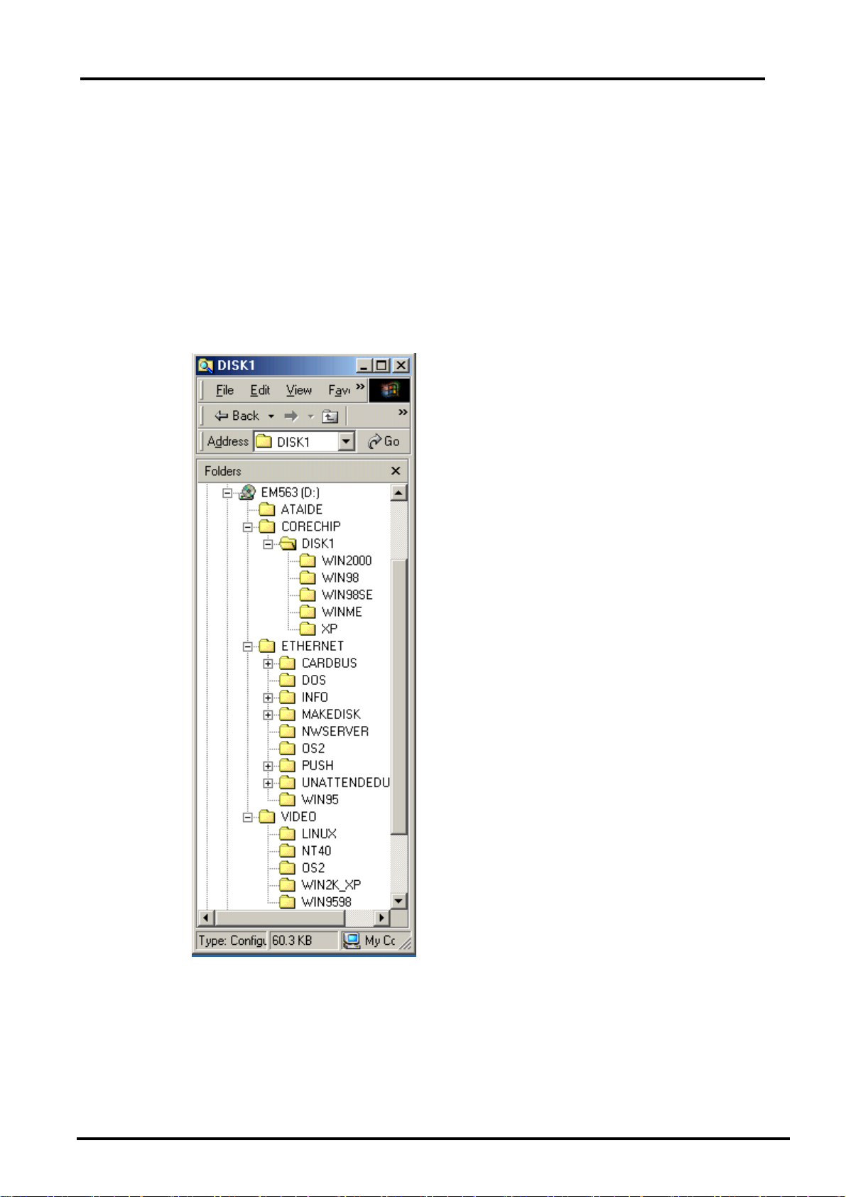
4.2 File Directory
35 User’s Manual
Page 40

Appendix A How to use watch-dog timer
APPENDIX A. How to u se watch-dog timer
To use the watch-dog timer :
Step 1. Enable and retrig ger the Watch-Dog timer : Output port 443H
Step 2. Disable : Output port 441H
EX.1: For DOS
Execute the DEBUG.EXE file under DOS, Then key-in O443. The system will reboot
automatically acc o rding to the time-ou t y o u set.
Enable Disable
C:\DOS> DEBUG C:\DOS> DEBUG
O 443 0~F O 441 0~F
EX.2: For assemble Language
Enable :
:
:
MOV DX, 443H
OUT DX , AL
:
:
Disable :
:
:
MOV DX, 441H
OUT DX , AL
:
36 User’s Manual
Page 41

Terms and Cond itions
Date:1997.10.20
Warranty Policy
1. All pr o ducts are warr anted ag ainst defects in m aterials and wor kmanship o n a period of two years from t he
date of purchase by the customer.
2. T he buye r will b ear t he return frei ght cha rges for go ods tha t are returned fo r repai r wit hin the wa rranty
perio d whereas m anufacturer will b ear the other way after repair.
3. The buyer will pay for repair (for the replaced materials plus service time) and transportation charges (both
ways) for items after the expiration of the warranty period.
4. If the RMA Service Request Form does not meet the stated requirement as listed on “RMA Service “ , RMA
goods will be returned at the customer expense.
5. The following conditions are excluded from this warranty:
A. Imp roper or inadequate m aintenance by the cu stomer.
B. Unauthorized modification or misuse.
C. Oper at io n outside o f the environmental specification s for the p roduc t.
RMA Service
1. Request a RMA#
Complete and fax to Supplier the “R MA Request Form” to obtain a R MA number.
2. Shipping:
A. The customer is requested to fill up the problem code as listed . If none of the code is selected,
please write the symptom description on the remark.
B. Ship the defective units with freight prepaid.
C. Mark the RM A # clearly on the box.
D. Ship ping damage as a result of inadequ ate packing is t he custom er‘s responsibility.
E. Use the original p acking materials whenev er possible .
3. A ll RMA# are va lid for 30 d ays only:
When RMA goods are received af ter valid RMA# period , the good s will be rejected .
:
Page 42

RMA Servi ce Request For m
When requesting RMA service, please fill out this “RMA Service Request Form”.
Withou t t h is form your RM A will be R EJ ECTED!!!
RMA No:
Company: Contact Person:
Phone No. Purchased Date:
F ax No.: Applied Date:
Return Shipping Address:
Shipping by: □Air Freight □Sea □Express : □Others:
Item Model Name Serial Nu m ber Con fig uration
Item Pro blem Code Failure Status
Reasons to Return: □ Repair (Please in clu de f ailur e details ) □ Te s t i ng
Purpose
*Problem Code:
01:D.O.A.
02: Second Time R.M.A.
03: CMOS Data Lost
04: FDC Fail
05: HDC Fail
06: Bad Slot
07: BIOS Problem
08: Key b oard C ontroller Fail
09: Cache RMA Problem
10: Memo ry Socket Bad
11: Hang Up Software
12: Out Look Damage
Request Party
Authorized Signatur es / Date Authorized Si gnatures / Date
13: SCSI
14: LPT Port
15: PS2
16: LAN
17: COM Port
18: Watchdog Timer
Confirmed B y Supplier
19: DIO
20: Buzzer
21: Shut Down
22: Panel Fail
23: CRT Fail
24: Others (Pls specify)
 Loading...