

Page 1

EM-561 SERIES
5.25” EMBEDDED SBC
WITH VGA & THREE 10/100MBPS LAN
FOR SOCKET370 PENTIUM III PROCESSOR
USER'S MANUAL
Page 2

COPYRIGHT
This document is a copyright of the original manufacturer, 2001. The original manufacturer
reserves the rights to make improvement and/or modification to the product described in this
manual at any time without further notice. This manual may not, in whole or in part, be
photocopied, reproduced, transcribed, translated, or transmitted in whatever form without the
written consent of the manufacturer, except for copies retained by the purchaser for backup
purposes. All rights are reserved.
©
TRADEMARKS
The following are trademarks or registered trademarks of their respective companies: IBM, Intel,
AMD, Cyrix, NS, Award, AMI, Microsoft, Windows, Windows NT, Novell, SCO, PC/104, PICMG, ALI,
UMC, SMC and Winbond. Products mentioned in this manual are mentioned for identification
purposes only. All names of products or services appearing in this manual are the trademarks or
registered trademarks of their respective organizations and companies.
ã Copyright 2001
Date: October 1st , 2001
Page 3

TABLE OF CONTENTS
CHAPTER 1 General Information …………………………………………..…… 1
1.1 Introduction ………………………………………………………………….……….. 1
1.2 Features ………………………………………………………………………..……….. 1
1.3 Specification ………………………………………………………………….……….. 2
1.4 Unpack Your EM-561 ………………………………………………………..…… 2
1.5 Board Layout …………………………………………………………………..……….. 3
CHAPTER 2 Installation ……………………………………………………………. 4
2.1 Hardware Setup and Installation ………………………..…………………… 4
2.1.1 CPU Installation and Upgrading ……………….…………………… 4
2.1.2 System Memory Installation ………………………………………… 5
2.1.3 DiskOnChip Installation ………………………..…………………….. 6
2.2 Jumper Settings And Connectors ………………………………………………. 6
2.2.1 Board Outline …………………………………………………….……… 6
2.2.2 Jumper Settings Summary ………………………………..…………. 7
2.2.3 I/O Connectors Summary ……………………………..……………… 10
CHAPTER 3 BIOS Setup ………………………………………………………… 26
3.1 Running Award BIOS………………………………………………………………. 26
3.2 CMOS Setup Utility …………………………………………………………………. 27
3.3 Standard CMOS Setup ……………………………………………………………… 28
3.4 BIOS Features Setup ……………………………………………………………….. 30
3.5 Chipset Features Setup ……………………………………………………………. 32
3.6 Integrated Peripherals …………………………………………………………….. 34
3.7 Power Management Setup ………………………………………………………. 36
3.8 PnP/PCI Configuration ……………………………………………………………… 39
3.9 PC Health Status ………………………………………………………………………. 40
3.10 Frequency / Voltage Control ……………………………………………………. 41
3.11 Load Fail-Safe Defaults …………………………………………………………….. 42
3.12 Load Optimized Defaults …………………………………………………………… 42
3.13 Supervisor / User Password …………………………………………………….. 43
3.14 Save & Exit Setup …………………………………………………………………….. 43
3.15 Exit Without Saving ………………………………………………………………….. 44
CHAPTER 4 Drivers Support ……………………………………………………… 45
4.1 Driver Support …………………………………………………………………………… 45
4.1.1 Core Chip ………………………………………………………………..……. 45
4.1.2 Network ……………………………………………………………………… 45
4.1.3 VGA ………………………………………………………………………….. 45
4.1.4 Hardware Monitor ………………………………………………………. 46
4.2 Driver List ………………………………………………………………………………. 46
4.3 Driver Setup and Installation ……………………………………………………. 47
4.3.1 Intel 815 Chipset ………………….…………………………….………. 47
4.3.2 Intel Ultra ATA Storage Driver ………………..……………………. 49
4.3.3 VGA Driver …………………..……………………………………………… 51
4.3.4 LAN Driver …………………….……………………………………………. 53
APPENDIX A How To Use Watch-Dog Timer
Terms and Condition
RMA Service Request Form
Page 4

Page 5

Page: 1
CHAPTER 1 General Information
1.1 Introduction
The new EM-561 Series embedded SBC is highly configurable with multiple features to suit
different types of commercial and industrial needs. Three Ethernet capability of the EM-561 Series
gives network administrators another tool to deal with today's changing application needs. The
board comes with the top-of-the-line Intel 82559 LAN chips could act as a firewall that sits
between the Internet and a company's internal network. This applies to Web (HTTP) servers, FTP
servers, SMTP (E-mail) servers or DNS servers. The EM-561 can also be used as an inter-network
gateway that connects a number of local networks. Once again, the three Ethernet capability and
processing power of the EM-561 Series gives it the ability to perform these functions.
The new EM-561 Series is enhanced with IntelÒ815E chipset; one 168-DIMM socket support up
to 100/133 MHz SDRAM and one DiskOnChip from M-System socket support up to 288MB flash
memory disk which provide full functionality and performance to be used "exactly" where you
need it as well. EM-561 also features high performance VGA display that support resolutions and
color depths up to 1600x1200 x256 color at 85Hz.
EM-561 has many expansion function such as one PCI expansion connector with one PCI riser
card; one FDD interface support up to two floppy devices ; two IDE ports that support up to four
IDE devices and Ultra ATA/100/66/33 interface helps designers and integrators improve system
performance by retrieving and sending data faster. Everything you could need is on-board.
In addition, it is equipped with two RS-232 serial ports; four USB ports; one multi-mode parallel
port which supports SPP, ECP and EPP modes. It provides more flexible functions to satisfy all
users' different application requirements.
The EM-561 also offers several industrial features such as a 16 -level watchdog time-out intervals
and contains the health monitoring hardware. The health monitoring IC keeps an eye on the
CPU and releases an audio alarm when detecting abnormal operating voltage & temperature or
malfunction of the cooling fans. And with its industrial grade reliability, the EM-561 can operate
continuously at temperatures up to 60° C (140° F). All these numerous features provide an ideal
price/performance solution for commercial and industrial applications where stability and reliability
are essential.
1.2 Features
n Supports Socket 370 Celeron/Intel® Pentium III Processor, 133MHz FSB
n Intel®815E chipset
n Built–in three 10/100BASE-TX Ports with RJ-45 connectors
n Socket for DiskOnChip
n With one PCI expansion slot
n 4 USB ports and supports 4 Ultra ATA 100 devices
n 5.25” Form Factor, special design for firewall and network applications
Page 6

1.3 Specification
EM-561 Series
Processor
Chipset
System Memory / RAM One 168-pin DIMM sockets, support 100/133 MHz SDRAM and up to
BIOS
Flash Memory Disk Reserved socket for DiskOnChip from M-System, support up to 288 MB
Graphics Controller Internal graphic controller with Intel’s Dynamic Video Memory
Network Interface Three Intel 82559 chip, support three-10/100 Base-TX Ethernet, three
IDE Drive Interface Two PCI IDE ports that support up to four IDE devices and Ultra
Floppy Drive Interface One FDD port, support up to two floppy devices
Serial Port Two COM ports, one RS-232 DB-9 connector and one RS-232
Parallel Port One multi-mode parallel port ( SPP / EPP / ECP )
Bus Interface PCI bus slot
RTC Internal RTC with Li battery
Keyboard/Mouse 6-pin keyboard/mouse pin header
Watchdog Timer 16-level time-out intervals
Universal Serial Bus Support 4 USB ports (4x5 pin headers)
Health Monitoring Enhanced hardware monitor functions with optical sensor
Operating Temperature
Storage Temperature
Humidity
Dimensions
EMI/EMS EN 50081-1/1994>EN 55022/1997>EN 61000-3-2/1995
Remark PCI Rev. 2.2 compliant
ORDERING INFORMATION EM-561B
EM-561C (Customer model No.)
IntelÒ Pentium III Coppermine / CeleronÔ Processor in Socket
370(66/100/133 MHz) and up to 1GB
IntelÒ 815E chipset
512 SDRAM
AwardÒ licensed BIOS
flash memory disk
Technology, resolution up to 1600 x 1200 x 256 colors @ 85 Hz, with
VGA 2x6x2.54 mm pin header with housing
RJ-45 external connectors with ACT LED, LNK LED
ATA/100/66/33
2x5x2.54 mm pin header with housing
0 °C~60 °C
-20 °C~70 °C
5 %~95% RH, non-condensing
203 x 146 x 25 mm ± 0.5 mm
>EN 61000-3-3/1995, EN 50082-1/1994>IEC 1000-4-2/1995,
IEC 1000-4-3/1995, IEC 1000-4-4/1995, EN55024
1.4 Unpack your EM-561
Before you begin to install your card, please make sure that you received the following materials as
listed below:
n EM-561 x 1 pc 5.25" Embedded Single Board Computer
n FDD Cable x 1 pc 34 to 34-pin Standard Header Flat Ribbon Cable
n IDE Cable x 1 pc 40-pin IDE Cable
n VGA Cable x 1 pc 12-pin Standard Header to 15-pin/3-Row D-Sub Cable
n Keyboard and Mouse Cable x 1 set 8-pin connector to PS/2 Keyboard and Mouse Cable
n Driver Utility CD-ROM x 1 pc Drivers & Utilities
n User's Manual x 1 pc This User's Manual
Page: 2
Page 7
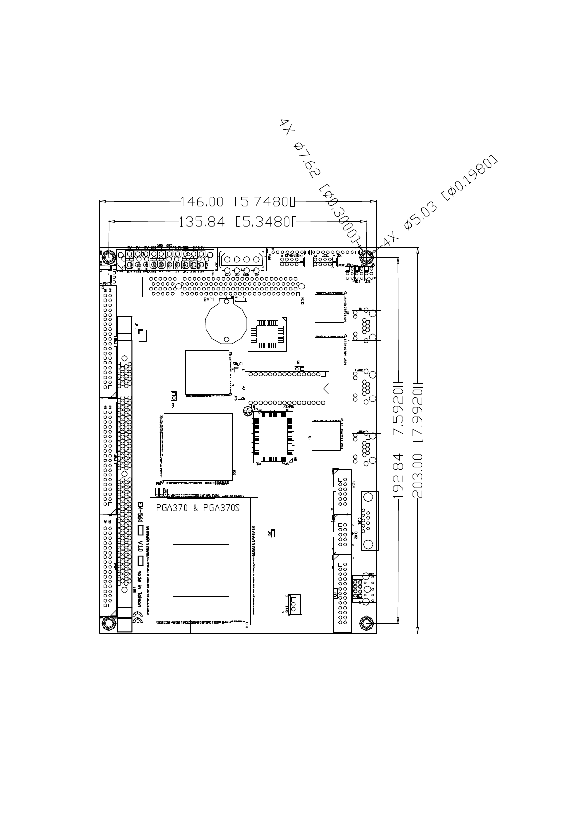
Page: 3
1.5 Board Layout
Page 8
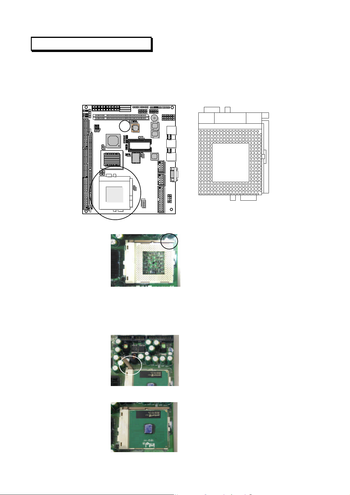
CHAPTER 2 Installation
2.1 Hardware Setup and Installation
2.1.1 CPU Installation and Upgrading
PGA370
Step 1: Locate the ZIF socket and open it by first pulling the lever of socket upward.
Step 2: Insert the CPU into the socket. Please keep the lever right angle when
inserting CPU.
Step 3: When inserting the CPU please note the correct orientation as shown. The
notched corner should point toward the end of the lever.
Step 4: Push the lever down to close the socket.
Page: 4
Page 9
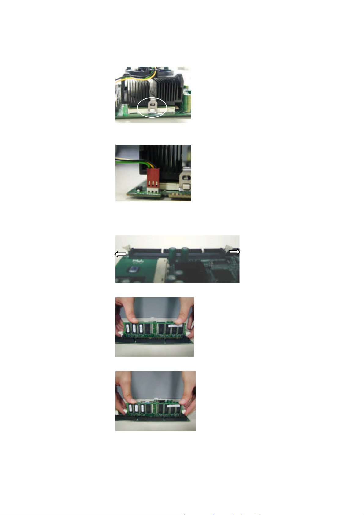
Page: 5
Step 5: Attach the heatsink onto the CPU.
Step 6: Push the clip of heatsink downward to hock the ear of socket firmly.
Step 7: Finally, attach the fan cable to the CPU fan header.
2.1.2 System Memory Installation
Step 1: Open latches of DIMM socket.
Step 2: Insert the RAM module into the DIMM socket.
Step 3: Press the latches into the notches of the RAM module.
Page 10

CON2
PWR1
IDE1
IDE2
FDC1
COM1
JP5
LAN1
CON1
JP3 JP2 JP1
JP12
JP15
ATXC1
JP13
JP6
SDOC1
PCI1
KM1
JP8
DIMI
JP10
JP11
SR1
ATXPS1
USB1
USB2
USB3
USB4
JP7
ATXPB1
JP9
LPT1
COM2
VGA1
FAN1
AT Power Connector 90。for EM-561C
PS1
2.1.3 DiskOnChip Installation
Please make sure the central polarization key on the socket, and place the DiskOnChip
as the same direction.
2.2 JUMPER SETTINGS AND CONNECTORS
2.2.1 Board Outline
JP14
CPU
LAN2
LAN3
Page: 6
Page 11

Page: 7
JP12,JP15
3 2 1
JP8
JP11
If you forget your password, the only
way to solve this problem is to
discharge the CMOS memory by turning
power off and placing a shunt on the S1
then
2.2.2 Jumper Settings Summary
LOCATION FUNCTION
JP8 Clear CMOS Data
JP11 Select CPU Clock
JP6 Flash FWH Chip
JP7 Case Open Detect
JP13, JP14 Programming ISP2032A
SDOC1 Select DiskOnChip (Flash Disk) Address
JP5, JP9, JP10,
l JP8: Clear CMOS Data
Description JP8
Normal (Default) 1-2
Clear CMOS 2-3
JP8
Note :
(open pad) for 5 seconds,
removing the shunt.
l JP11: Select CPU Clock
CPU Clock Speed JP11
66MHz 3-5,4-6
100MHz 1-3,4-6
100/133MHz(Default) 1-3,2-4
Factory use only
JP11
1
3
5
2
4
6
Page 12
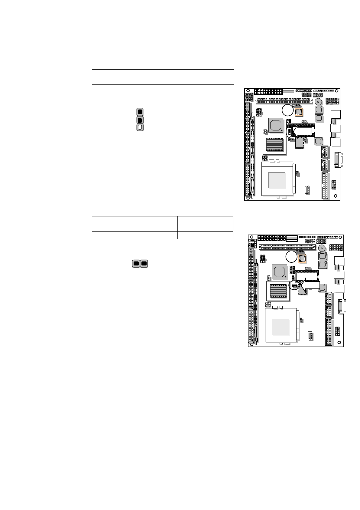
2
JP6
JP7
l JP6 : Flash FWH Chip
Flash FWH chip JP6
Unlocked (Default) 1-2
Locked 2-3
JP6
1
3
l JP7: Case Open Detect
Case Open Detect JP7
Enable (Default) ON
Disable OFF
JP7
Page: 8
Page 13

Page: 9
3 2 1
JP13
JP14
SDOC1
l JP13, JP14: Programming ISP2032A
Programming ISP2032A JP13,JP14
Normal (Default) 1-2
Programming 3-4
JP13, JP14
DOC1 : Select DiskOnChip ( Flash Disk ) Address
Flash Disk Address Sdoc1
CC00~CDFFH 1-2,9-10
D000 ~D1FFH 3-4,7-8
D400 ~D5FFH 3-4,9-10
D800 ~D9FFH 5-6,7-8
DC00~DDFFH 5-6,9-10
CC00~CDFFH
D000~D1FFH
D400~D5FFH
D800~D9FFH
DC00~DDFFH
(Default )
SDOC1
1
3
5
7
9
2
4
6
8
10
Page 14

2.2.3 I/O Connectors Summary
LOCATION FUNCTION
LAN1 LAN Connector
LAN2 LAN Connector
LAN3 LAN Connector
PS1 AT Power Connector
KM1 PS/2 Keyboard & Mouse Connector
PWR1 HDD Power Connector
ATXB1 ATX Power(On/Off) Header
ATXC1 ATX Power Header
JP1、JP2、JP3 Extension LAN LED
FAN1 CPU FAN Connector
COM1 RS-232 Serial Port #1 Connector
COM2 Serial Port #2 Connector
CON1 Power LED, Reset, Speaker Connector
USB1、2、3、4 USB Port#1 & #2 & #3 & #4 Connector
FDC1 Floppy Interface Connector
VGA1 VGA Connector
ATXPS1 ATX Power Connector
LPT1 Parallel Port Connector
IDE1 Primary IDE Cable Connector
IDE2 Secondary IDE Cable Connector
PCI1 PCI Slot
SR1 System Status Signal (port 440)
Page: 10
Page 15
Page: 11
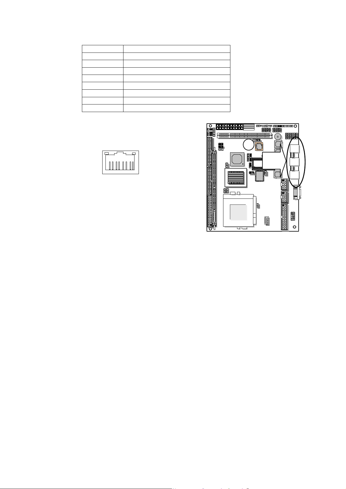
LAN1
LAN1, LAN2, LAN3 : LAN Connector
Pin No. Description
1 TX+
2 TX3 RX+
4 NC
5 NC
6 RX7 NC
8 NC
LAN1, LAN2, LAN3
8
1
LAN2
LAN3
Page 16
26 13
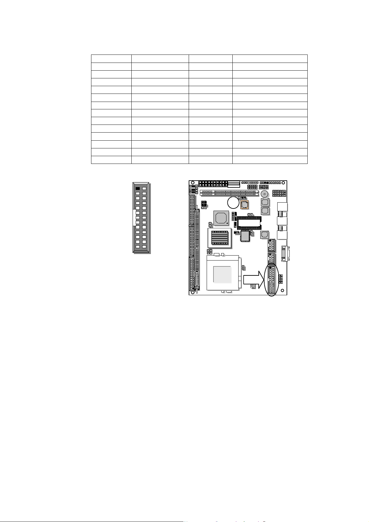
LPT1
l LPT1:Parallel Connector ( Header )
PIN NO. DESCRIPTION PIN NO. DESCRIPTION
1 Strobe # 14 Auto Form Feed
2 Data0 15 Error #
3 Data1 16 Initialize #
4 Data2 17 Printer Select IN #
5 Data3 18 Ground
6 Data4 19 Ground
7 Data5 20 Ground
8 Data6 21 Ground
9 Data7 22 Ground
10 Acknowledge # 23 Ground
11 Busy 24 Ground
12 Paper Empty 25 Ground
13 Printer Select 26 NC
LPT1
1
14
Page: 12
Page 17
Page: 13
3
5
KM1
PWR1
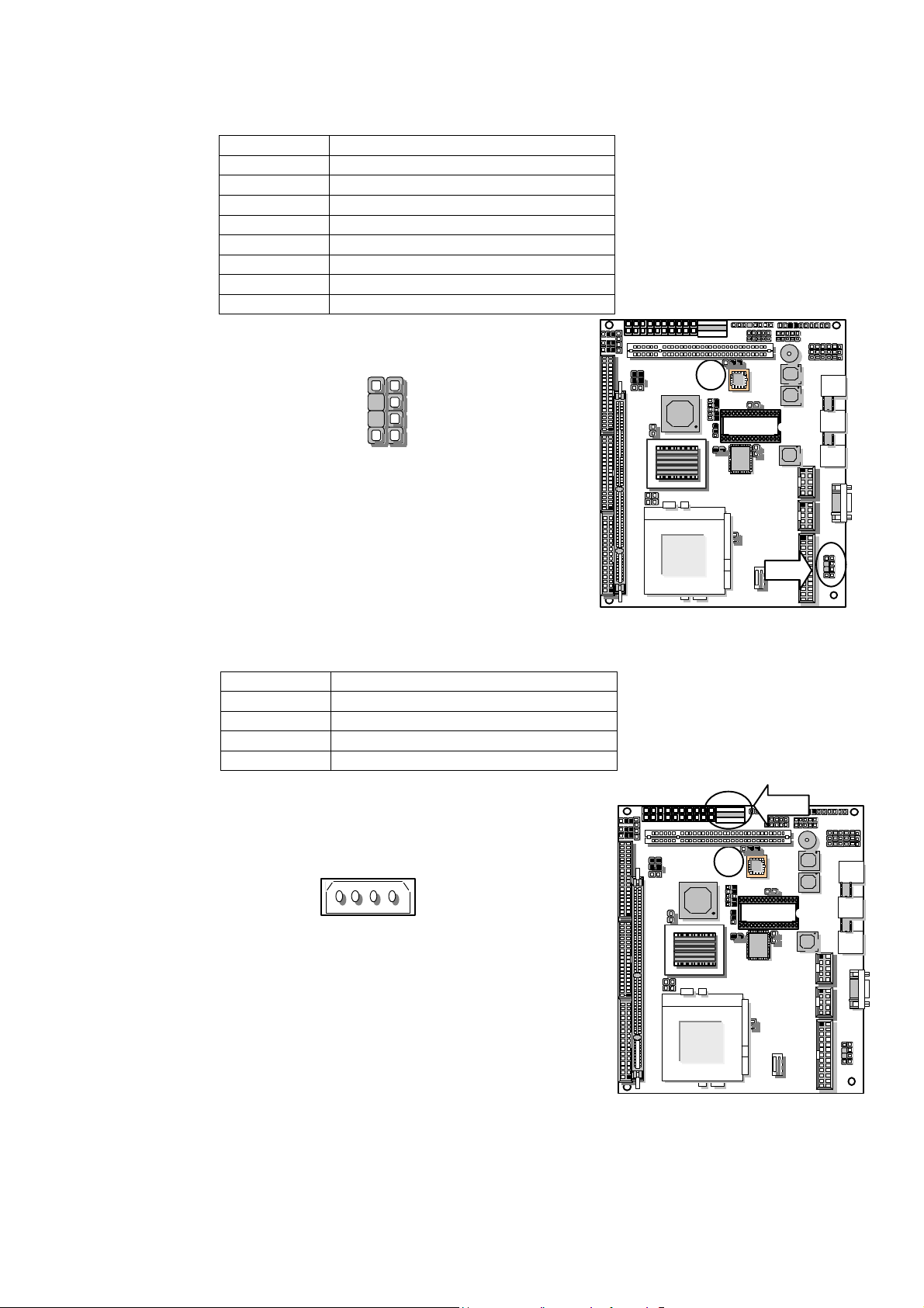
l KM1 : PS/2 Keyboard & Mouse Connector
Pin No. Description
1 Keyboard Data
2 Mouse Data
3 Ground
4 +5V
5 Keyboard Clock
6 Mouse Clock
7 NC
8 NC
KM1
7
8
6
1
2
4
l PWR1 : HDD Power Connector
Pin No. Description
1 +5V
2 Ground
3 Ground
4 +12V
PWR1
1 2 3 4
Page 18
ATXPB1
ATXC1
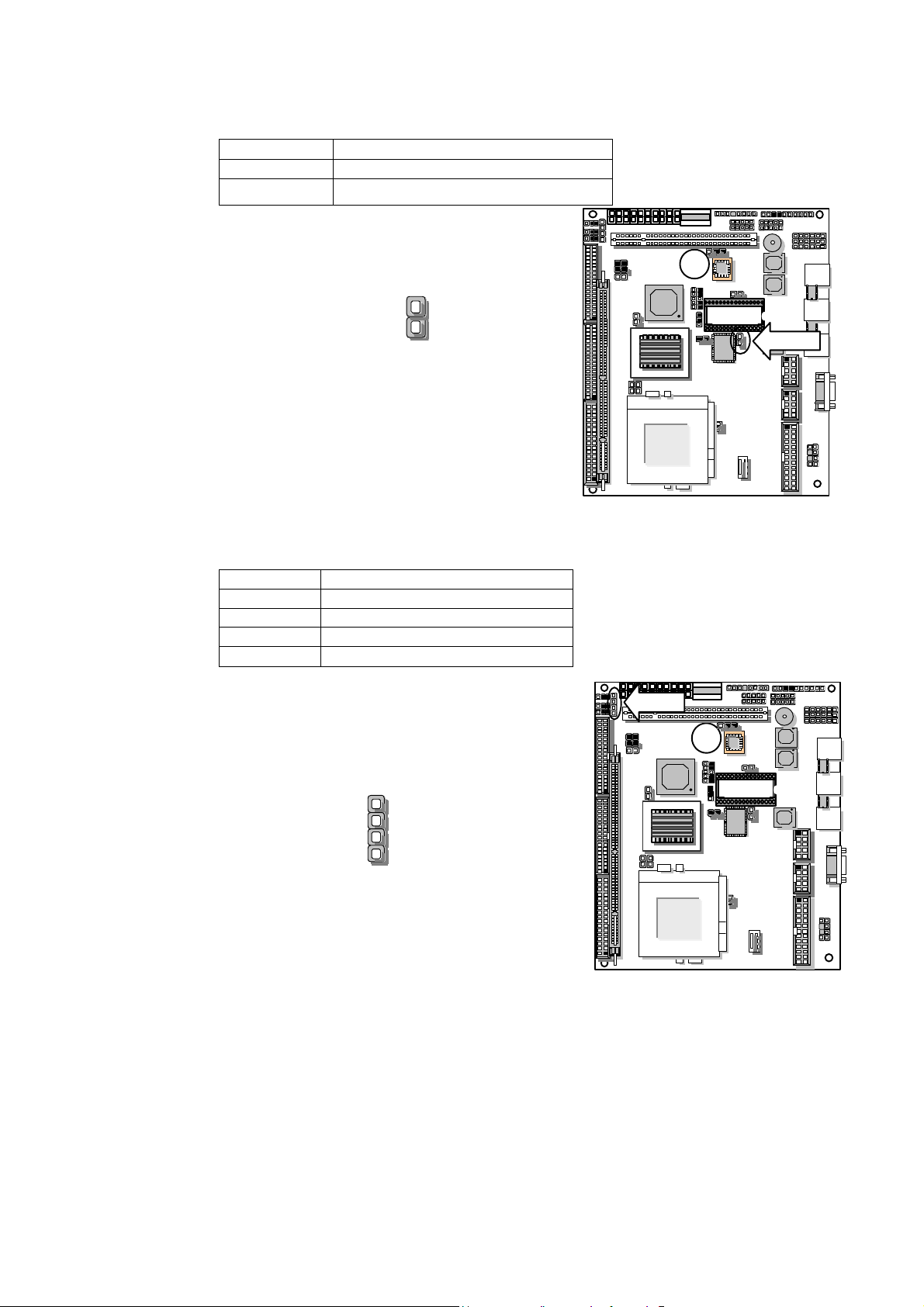
ATXB1: ATX Power(On/Off) Header
Pin No. Description
1 PANSW
2 GND
ATXB1
1
2
ATXC1: ATX Power Header
Pin No. Description
1 GND
2 Standby 5V
3 GND
4 PSON
ATXC1
1
4
Page: 14
Page 19

Page: 15
2
4
6
2
JP3
FAN1
JP1
Pin No. Description
、
JP2、JP3:Extension LAN LED
1 10/100M LED2 10/100M LED+
3 LINK LED4 LINK LED+
5 Active LED6 Active LED
JP1, JP2, JP3
1
3
5
JP1
JP2
FAN1: CPU FAN Connector
Pin No. Description
1 Ground
2 +12V
3 FAN Status Signal
FAN1
1
3
Page 20
10
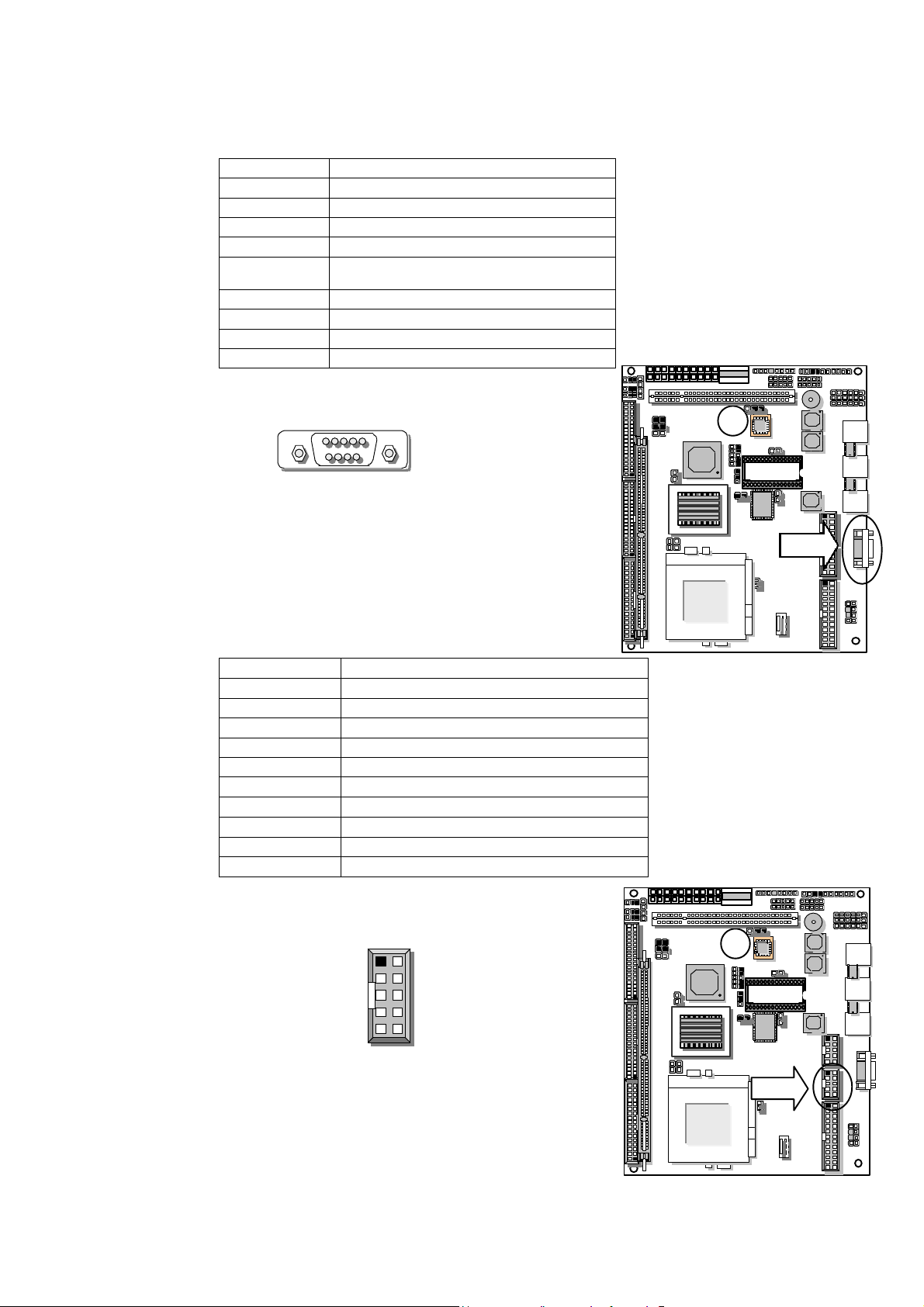
COM1
COM2
l COM1 : RS-232 Serial Port #1 Connector ( D-Sub )
Pin No. Description
1 Data Carrier Detect ( DCDA # )
2 Receive Data ( RXDA )
3 Transmit Data ( TXDA )
4 Data Terminal Ready ( DTRA # )
5 Ground ( GND )
6 Data Set Ready ( DSRA # )
7 Request To Send ( RTSA # )
8 Clear To Send ( CTSA # )
9 Ring Indicator ( RIA # )
1
6
COM1
5
9
l COM2 : Serial Port #2 Connector ( Header )
Pin No. Description
1 Data Carrier Detect (DCDB #)
2 Receive Data (RXDB)
3 Transmit Data (TXDB)
4 Data Terminal Ready (DTRB #)
5 Ground
6 Data Set Ready (DSRB #)
7 Request To Send (RTSB #)
8 Clear To Send (CTSB #)
9 Ring Indicator (RIB #)
10 NC
COM2
1
2
9
Page: 16
Page 21
Page: 17
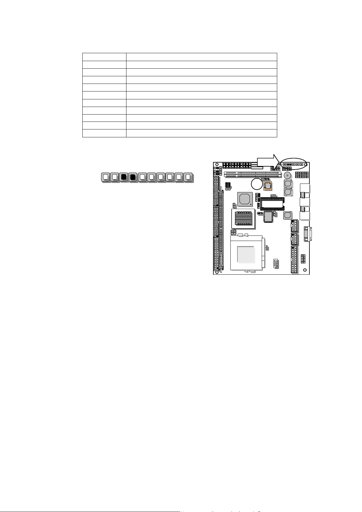
CON1
l CON1 : Power LED, Reset, Speaker Connector
Pin No. Description
1 Power LED +
2 GND
3 HDD LED +
4 HDD LED 5 RESET SW +
6 RESET SW – (GND)
7 External Speaker 8 Internal Buzzer 9 NC
10 External Speaker +
CON1
10
Default : 7-8 (ON)
Internal Buzzer
1
Page 22
USB1
USB2
USB3
USB1
USB1
USB2
USB3
USB4
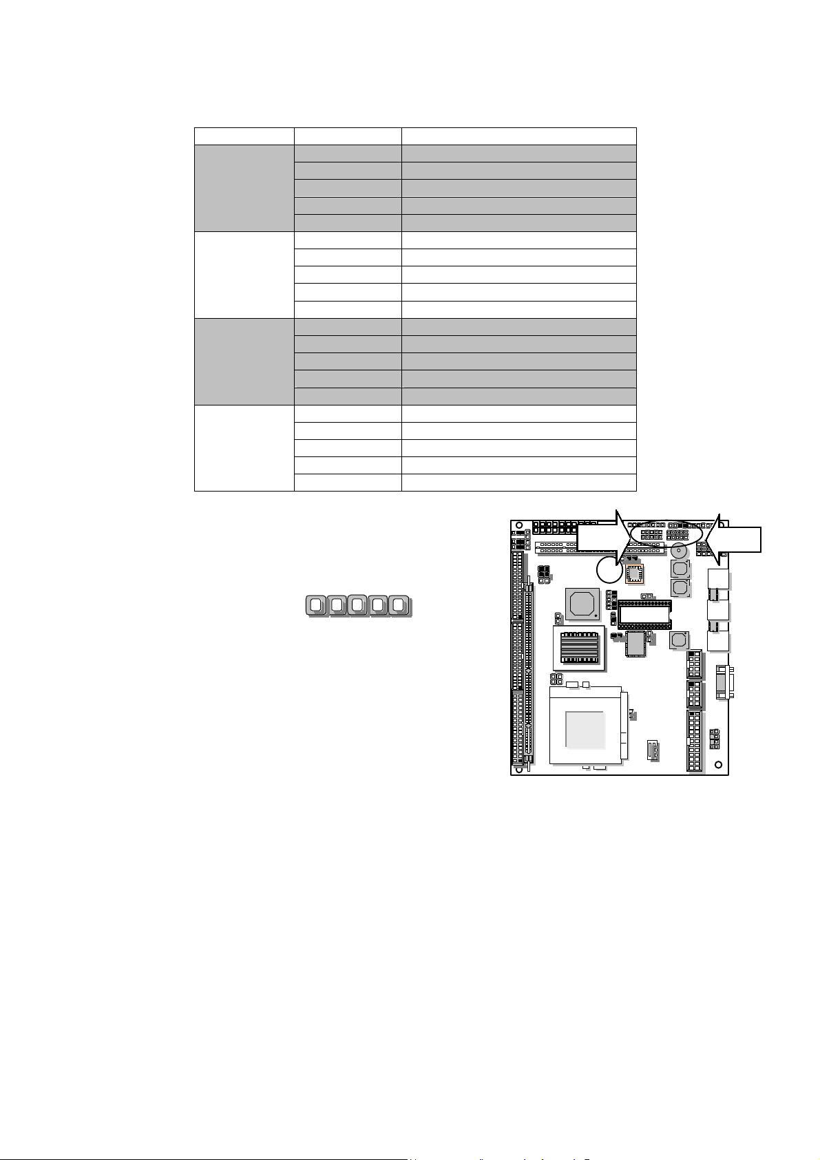
、2、3、4:
USB Port#1 & #2 & #3 & #4 Connector
Pin No. Description
1 USB Port#1 Vcc
2 USB D03 USB D0+
4 Ground
5 USB Port#1 Vcc
1 USB Port#2 Vcc
2 USB D13 USB D1+
4 Ground
5 USB Port#2 Vcc
1 USB Port#3 Vcc
2 USB D23 USB D2+
4 Ground
5 USB Port#3 Vcc
1 USB Port#4 Vcc
2 USB D33 USB D3+
4 Ground
5 USB Port#4 Vcc
USB1, USB2, USB3, USB4
5
1
USB4
Page: 18
Page 23

Page: 19
FDC1
FDC1 : Floppy Interface Connector ( Header )
Pin No. Description Pin No. Description
1 Ground 2 Density Select
3 Ground 4 NC
5 Ground 6 NC
7 Ground 8 Index #
9 Ground 10 Motor Enable A #
11 Ground 12 Drive Select B #
13 Ground 14 Drive Select A #
15 Ground 16 Motor Enable B #
17 Ground 18 Direction #
19 Ground 20 Step #
21 Ground 22 Write Data #
23 Ground 24 Write Gate #
25 Ground 26 Track 0 #
27 Ground 28 Write Protect #
29 NC 30 Read Data #
31 Ground 32 Head Side Select #
33 NC 34 Disk Change #
34
33
FDC1
1 2
Page 24
12
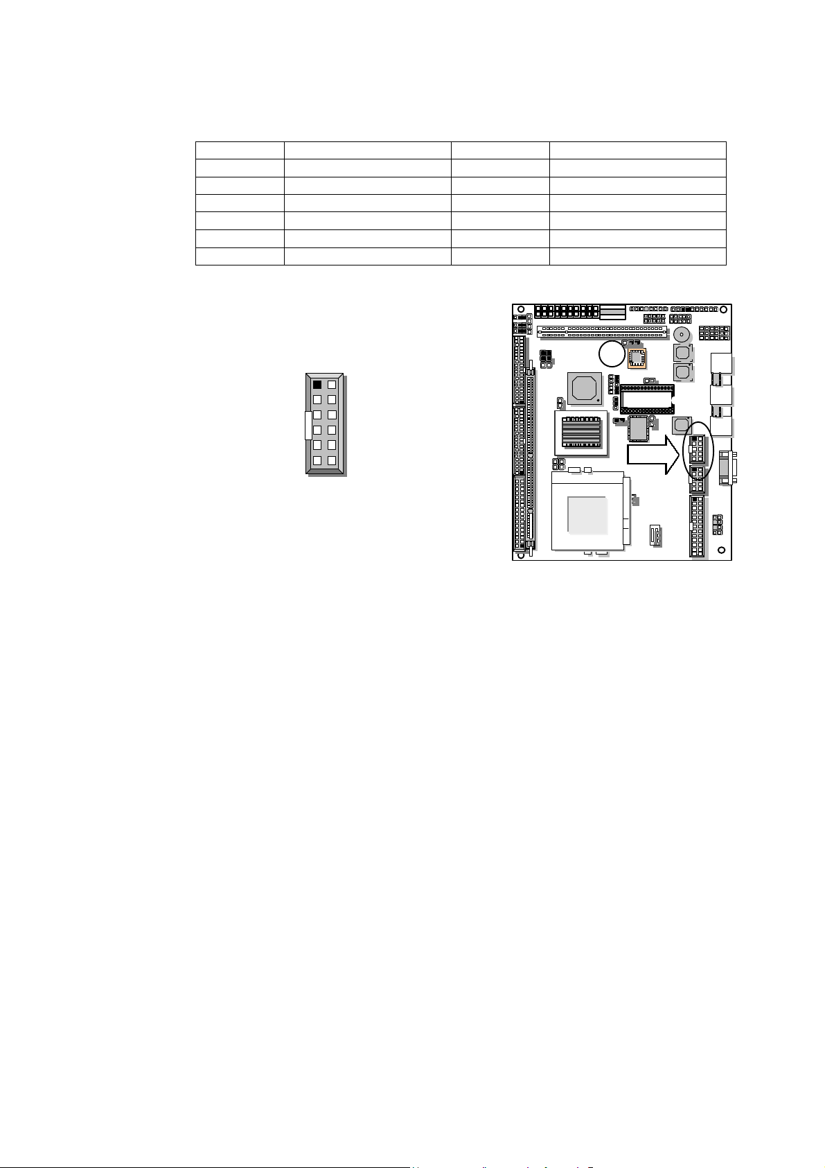
VGA1
VGA1 : VGA Connector
Pin No. Description Pin No. Description
1 Red Signal 2 Ground
3 Green Signal 4 Ground
5 Blue Signal 6 Ground
7 H-SYNC 8 Ground
9 V-SYNC 10 Ground
11 DDC-DATA 12 DDC-Clock
VGA1
11
1
2
Page: 20
Page 25

Page: 21
1
10
ATXPS1
ATXPS1 : ATX Connector
Pin No. Description Pin No. Description
1 VCC3 11 VCC3
2 VCC3 12 - 12V
3 GND 13 GND
4 +5V 14 Power On Switch
5 GND 15 GND
6 +5V 16 GND
7 GND 17 GND
8 Power Good 18 - 5V
9 +5V Stand By 19 +5V
10 + 12V 20 +5V
20
l PS1: AT Power Connector (For EM-561C only)
Pin No. Description
1 Power Good
2 +5V
3 +12V
4 -12V
5 GND
6 GND
7 GND
8 GND
9 -5V
10 +5V
11 +5V
12 +5V
1 12
ATXPS1
2
PS1
Page 26
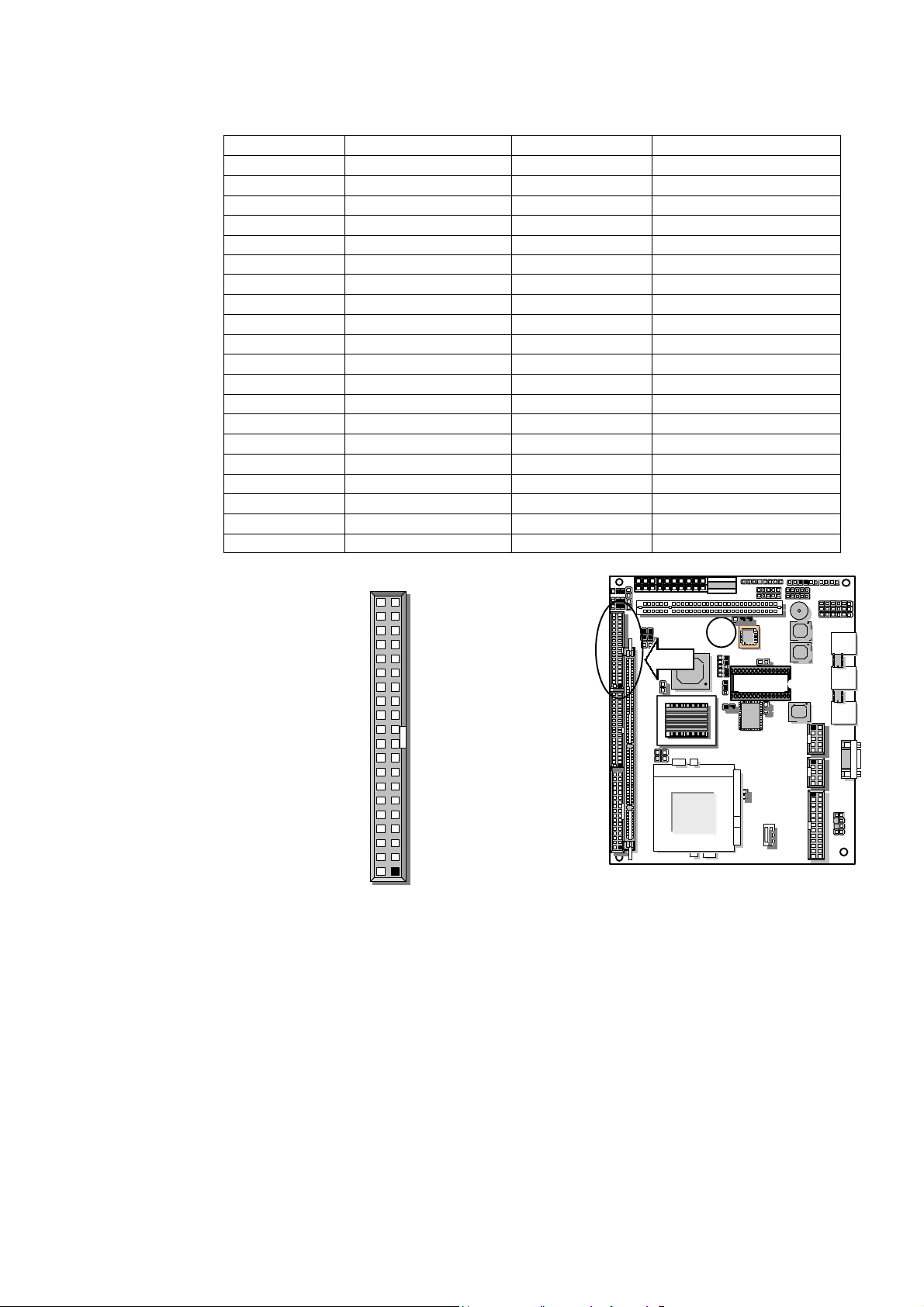
IDE1
l IDE1 : Primary IDE Cable Connector ( Header )
Pin No. Description Pin No. Description
1 Reset # 2 Ground
3 Data 7 4 Data 8
5 Data 6 6 Data 9
7 Data 5 8 Data 10
9 Data 4 10 Data 11
11 Data 3 12 Data 12
13 Data 2 14 Data 13
15 Data 1 16 Data 14
17 Data 0 18 Data 15
19 Ground 20 NC
21 DMA REQ 22 Ground
23 IOW # 24 Ground
25 IOR # 26 Ground
27 IOCHRDY 28 NC
29 DMA ACK # 30 Ground
31 Interrupt 32 IOCS16 #
33 SA1 34 DMA66 Detect
35 SA0 36 SA2
37 HDC CS0 # 38 HDC CS1 #
39 HDD Active LED # 40 Ground
40
39
IDE1
2
1
Page: 22
Page 27
Page: 23
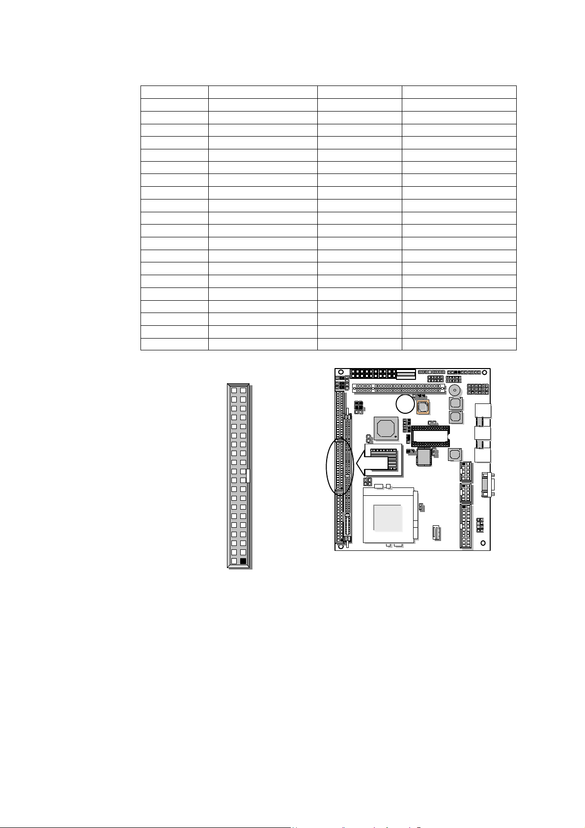
IDE2
l IDE2 : Secondary IDE Cable Connector ( Header )
Pin No. Description Pin No. Description
1 Reset # 2 Ground
3 Data 7 4 Data 8
5 Data 6 6 Data 9
7 Data 5 8 Data 10
9 Data 4 10 Data 11
11 Data 3 12 Data 12
13 Data 2 14 Data 13
15 Data 1 16 Data 14
17 Data 0 18 Data 15
19 Ground 20 NC
21 DMA REQ 22 Ground
23 IOW # 24 Ground
25 IOR # 26 Ground
27 IOCHRDY 28 NC
29 DMA ACK # 30 Ground
31 Interrupt 32 IOCS16 #
33 SA1 34 DMA66 Detect
35 SA0 36 SA2
37 HDC CS0 # 38 HDC CS1 #
39 HDD Active LED# 40 Ground
40
39
IDE2
2
1
Page 28

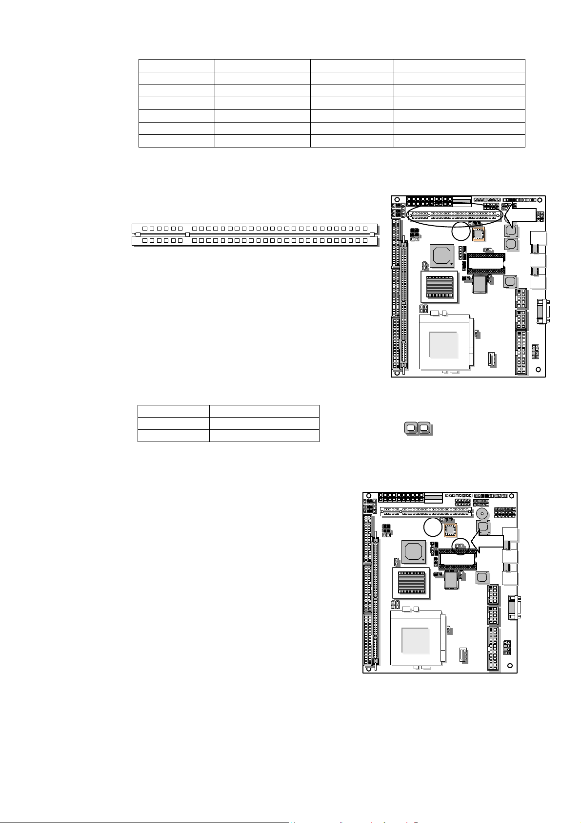
l PCI1: PCI SLOT
Pin No. Description Pin No. Description
A1 TRST# B1 -12V
A2 +12V B2 TCK
A3 TMS B3 GND
A4 TDI B4 TDO
A5 +5V B5 +5V
A6 INTA# B6 +5V
A7 INTC# B7 INTB#
A8 +5V B8 INTD#
A9 RSVD B9 PRST1#
A10 5V/IO B10 RSVD
A11 RSVD B11 PRST2#
A12 GND B12 GND
A13 GND B13 GND
A14 RSVD B14 RSVD
A15 RST# B15 GND
A16 5V/IO B16 CLK
A17 GNT# B17 GND
A18 GND B18 REQ#
A19 RSVD B19 5V/IO
A20 AD30 B20 AD31
A21 +3.3V B21 AD29
A22 AD28 B22 GND
A23 AD26 B23 AD27
A24 GND B24 AD25
A25 AD24 B25 +3.3V
A26 IDSEL B26 C/BE3#
A27 +3.3V B27 AD23
A28 AD22 B28 GND
A29 AD20 B29 AD21
A30 GND B30 AD19
A31 AD18 B31 +3.3V
A32 AD16 B32 AD17
A33 +3.3V B33 C/BE2#
A34 FRAME# B34 GND
A35 GND B35 IRDY#
A36 TRDY# B36 +3.3V
A37 GND B37 DEVSL#
A38 STOP# B38 GND
A39 +3.3V B39 LOCK#
A40 SDONE B40 PERR#
A41 SBO# B41 +3.3V
A42 GND B42 SERR#
A43 PAR B43 +3.3V
A44 AD15 B43 C/BE#
A45 +3.3V B44 AD14
A46 AD13 B45 GND
A47 AD11 B46 AD12
A48 GND B48 AD10
A49 AD9 B49 GND
A52 C/BE0# B52 AD8
A53 +3.3V B53 AD7
A54 AD6 B54 +3.3V
A55 AD4 B55 AD5
A56 GND B56 AD3
Page: 24
Page 29
Page: 25
PCI1
SR1
Pin No. Description Pin No. Description
A57 AD2 B57 GND
A58 AD0 B58 AD1
A59 5V/IO B59 5V/IO
A60 REQ64# B60 ACK64#
A61 +5V B61 +5V
A62 +5V B62 +5V
PCI1
B1 B62
A62
A1
SR1: System Status Signal (Port 440)
Pin No. Description
1 LED + Signal
2 LED - Signal
EX. For System Status Signal (Port 440 , bit 3)
C:\DOS> DEBUG
-O 440 8
SR1 LED always on
C:\DOS> DEBUG
-O 440 0
SR1 LED flashing
SR1
2 1
Page 30

CHAPTER 3. Bios Setup
Award‘s ROM BIOS provides a built-in Setup program that allows user to modify the basic system
configuration and settings. The modified data will be stored in a battery-backed CMOS RAM so that these
data will be retained even when the power is turned off. In general, the information saved in the CMOS
RAM stay unchanged unless there is configuration change in the system, such as hard drive replacement or
new equipment is installed.
3.1 Running AWARD BIOS
The Setup Utility is stored in the BIOS ROM. When the power of the computer system is turned
on, a screen message appears to give you an opportunity to call up the Setup Utility; while the
BIOS will enter the Power On Self Test (POST) routines. The POST routines perform various
diagnostic checks while initializing the board hardware. If the routines encounter an error
during the tests, the error will be reported in either of the two different ways, hear a series of
short beeps or see an error message on the screen display. There are two kinds of error: fatal
or non-fatal. The system can usually continue to boot up sequence with the non-fatal errors.
Non-fatal error messages usually appear on the screen along with the following instructions:
“ Press <F1> to RESUME ”
Write down the message and press the F1 key to continue the boot up sequence. After the
POST routines are completed, the following message appears:
“ Press DEL to enter SETUP ”
Entering Setup
Turn on the power of the computer system and press <Del> immediately. If you don’t have the
chance to respond, reset the system by simultaneously typing the <Ctrl>, <Alt> and <Delete>
keys, or by pushing the ‘ Reset ’ button on the system cabinet. You can also restart by turning
the system OFF then ON.
Page: 26
Page 31

Page: 27
3.2 CMOS Setup Utility
To access the AWARD BIOS SETUP program, press the <DEL> key. The screen display will
appears as shown below:
Main Program Screen
CMOS Setup Utility – Copyright © 1984-2001 Award Software
Standard CMOS Features
Advanced BIOS Features Load Fail-Safe Defaults
Advanced Chipset Features Load Optimized Defaults
Integrated Peripherals Set Supervisor Password
Power Management Setup Set User Password
PnP/ PCI Configurations Save & Exit Setup
PC Health Status Exit Without Saving
Esc : Quit
F10 : Save & Exit Setup
Time, Date, Hard Disk Type....
This screen provides access to the utility‘s various functions.
Listed below is explanation of the keys displayed at the bottom of the screen:
<ESC> : Exit the utility.
<á â à ß> Use arrow keys á â à ß to move cursor to your desired selection.
<F1> General Help
<F5> Previous Values
<F6> Fail-Safe Defaults
<F7> Optimized Defaults
<F10> Saves all changes made to Setup and exits program.
+/-/PU/PD Change Value
Standard CMOS Setup: Use this menu for basic system configurations.
Advanced BIOS Features: Use this menu to set the Advanced Features available on your
system.
Advanced Chipset Features: Use this menu to change the values in the chipset registers and
optimize your system’s performance.
Integrated Peripherals: Use this menu to specify your settings for integrated peripherals.
PnP/PCI Configuration: This entry appears if your system supports PnP/PCI.
PC Health Status: This entry shows your PC health status. If Hardware Monitor Chipset is
installed.
Frequency / Voltage Control: Use this menu to specify your settings for frequency / voltage
control.
Load Fail-Safe Defaults: Use this menu to load the BIOS default values for the
minimal/settings for optimal performance system operations.
Frequency/Voltage Control
á â àß
: Select Item
Page 32

Change the day, month,
Load Optimized Defaults: Use this menu to load the BIOS default values that are factory
settings for optimal performance system operations.
Set Supervisor Password: Use this menu to set Supervisor Passwords.
Set User Password: Use this menu to set User Passwords.
Save & Exit Setup: Save CMOS value changes to CMOS and exit setup.
Exit Without Saving: Abandon all CMOS value changes and exit setup.
3.3 Standard CMOS Setup
When you select the “STANDARD CMOS SETUP” on the main program, the screen display will
appears as :
Standard CMOS Setup Screen
Date (mm:dd:yy) Fri, Sep 7 2001 Item Help
Time (hh:mm:ss) 16 : 33 : 54
Drive A 1.44M, 3.5 in.
Drive B None
Video EGA/VGA
Halt On No, Errors
Base Memory 640K
Extended Memory 260096K
Total Memory 261120K
á â àß Move Enter: Select +/-/PU/PD: Value F10: Save Esc: Exit F1: General Help
The Standard CMOS Setup utility is used to configure the following components such as date,
time, hard disk drive, floppy drive, display and memory. Once a field is highlighted, on-line help
information is displayed in the left bottom of the Menu screen.
Date : Month, Date, Year.
Time : Hour, Minute and Second. Use 24-hour clock format (for p.m. time, add 12 to the hour
number, e.g. you would enter 4:30 p.m. as 16:30). When you select the “STANDARD CMOS
SETUP” on the main program, the screen display will appears as:
Primary Master / Primary Slave
Secondary Master / Secondary Slave: Press PgUp / <+> or PgDn / <-> to select Manual,
None, Auto type. Note that the specifications of your drive must match with the drive table.
The hard disk will not work properly if you enter improper information for this category. If your
hard disk drive type is not matched or listed, you can use Manual to define your own drive type
manually.
CMOS Setup Utility – Copyright © 1984-2001 Award Software
IDE Primary Master None
IDE Primary Slave None
IDE Secondary Master None
IDE Secondary Slave None
F5: Previous Values F6: Fail-Safe Defaults F7: Optimized Defaults
Standard CMOS Features
Menu Level
year and century
Page: 28
Page 33

Page: 29
The system boot will not stop for a keyboard or disk error ; it will stop
If you select Manual, related information is asked to be entered to the following items. Enter
the information directly from the keyboard. This information should be provided in the
documentation from your hard disk vendor or the system manufacturer.
If the controller of HDD interface is SCSI, the selection shall be
“None”
If the controller of HDD interface is CD-ROM, the selection shall be
“None”
Here is a brief explanation of drive specifications:
l Access Mode: The settings are Auto, Normal, Large, LBA.
l Cylinder: Number of cylinders
l Head: Number of heads
l Precomp: Write precomp
l Landing Zone: Landing Zone
l Sector: Number of sectors
Drive A and Drive B : Select the correct specifications for the diskette drive(s) installed in the
computer.
None No diskette drive installed
360K, 5.25 in 5-1/4 inch PC-type standard drive; 360 kilobyte capacity
1.2M, 5.25 in 5-1/4 inch AT-type high-density drive; 1.2 megabyte capacity
720K, 3.5in 3 1-2 inch double-sided drive; 720 kilobyte capacity
1.44M, 3.5 in 3 1-2 inch double-sided drive; 1.44 megabyte capacity
2.88M, 3.5 in 3 1-2 inch double-sided drive; 2.88 megabyte capacity
Note : 1. Not Installed could be used as an option for diskless workstations..
2.Highlight the listing after each drive name and select the appropriate entry.
Video : Select the type of primary video subsystem in your computer. The BIOS usually detects
the correct video type automatically. The BIOS supports a secondary video subsystem, but you do
not select it in Setup.
EGA/VGA Enhanced Graphics Adapter/Video Graphics Array.
For EGA, VGA, SEGA, SVGA or PGA monitor adapters.
CGA 40 Color Graphics Adapter, power up in 40 column mode
CGA 80 Color Graphics Adapter, power up in 80 column mode
MONO Monochrome adapter, includes high resolution monochrome adapters
Halt On : During the power-on-self-test (POST), the computer stops if the BIOS detects a
hardware error. You can tell the BIOS to ignore certain errors POST and continue the boot-up
process. These are the selections:
No errors Whenever the BIOS detects a non-fatal error the system will not be
stopped and you will be prompted
All errors The system boot will be stopped for any error that may be detected.
All, But Keyboard The system boot will not stop for a keyboard error ; it will stop for all
Other errors.
All, But Diskette The system boot will not stop for a disk error ; it will stop for all other
Errors.
All, But Disk/Key
for all other errors.
Base / Extended / Total Memory: The three items show the memory status of your system
(read only).
Page 34

X
3.4 Advanced BIOS Features Setup
When you select the “BIOS FEATURES SETUP” on the main program, the screen display will
appears as:
Advanced BIOS Features Setup Screen
CMOS Setup Utility – Copyright © 1984-2001 Award Software
Advanced BIOS Features
Virus Warning
CPU Internal Cache
External Cache
CPU L2 Cache ECC Checking
Processor Number Feature
Quick Power On Self Test
First Boot Device
Second Boot Device
Third Boot Device
Boot Other Device
Swap Floppy Drive
Boot Up Floppy Seek
Boot Up NumLock Status
Gate A20 Option
Typematic Rate Setting
Typematic Rate (Chars/Sec)
X
Typematic Delay (Msec)
Security Option
OS Select For DRAM >64MB
Report No FDD for WIN 95
Small Logo (EPA) Show
á â àß Move Enter: Select +/-/PU/PD: Value F10: Save Esc: Exit F1: General Help
F5: Previous Values F6: Fail-Safe Defaults F7: Optimized Defaults
Virus Warning : The default setting of the Virus Warning is “Disabled”. When it is enabled, any
attempt to write the boot sector and partition table will halt the system and cause a warning
message to appear. If this happens, you can use an anti-virus utility on a virus free, bootable
floppy diskette to reboot, to clean and to investigate your system.
CPU Internal Cache : The default setting is “Enabled”. This setting enables the CPU internal
cache.
External Cache : The default setting is “Enabled”. This setting enables the external cache.
CPU L2 Cache ECC Checking : The default setting is “Enabled”. When you select Enabled,
memory checking is enabled when the external cache contains ECC SRAMs.
Processor Number Feature : The default setting is “Enabled”. Enable to show the Pentium !!!
CPU serial number.
Quick Power On Self Test : The default setting is “Enabled”. This speeds up the Power On
Self Test (POST) by skipping some items that are normally checked during the full POST. If your
system is functioning normally, you can choose this feature to speed up the booting process.
First / Second / Third / Other Boot Device : The BIOS attempts to load the operating
system from the devices in the sequence selected in these items. The settings are Floppy,
Disabled
Enabled
Enabled
Enabled
Enabled
Enabled
Floppy
HDD-0
CDROM
Enabled
Disabled
Disabled
On
Fast
Disabled
6
250
Setup
Non-OS2
No
Disabled
Item Help
Menu Level
Allows you to choose
the VIRUS warning
feature for IDE Hard
Disk boot sector
protection. If this
function is enabled
and someone attempt
to write data into this
area, BIOS will show a
warning message on
screen and alarm
beep.
Page: 30
Page 35

Page: 31
LS/ZIP, HDD-0/HDD-1/HDD-2/HDD-3, SCSI, CDROM, LAN, and Disabled
Swap Floppy Drive : The default setting is “Disabled”. This setting gives you an option to
swap A and B floppy disks. Normally, the floppy drive A is the one at the end of the cable and
drive B is at the other end. If you set this option to “Enabled”, the Drive A will function as Drive
B, and vice-versa under the DOS.
Boot Up Floppy Seek : The defaults setting is “Disabled”. When enabled, the BIOS will check
whether there is a floppy disk drive installed.
Boot Up NumLock Status : The default setting is “On”. If set “Off”, the cursor controls will
function on the numeric keypad.
Gate A20 Option : The default setting is “Fast”. This is the optimal setting for the CPU card.
The other option is “Normal”.
Typematic Rate Setting : The default setting is “Disabled”. If enabled, you can set the
typematic rate and typematic delay.
Typematic Rate (Chars/Sec) : This setting controls the speed at which the system registers
the repeated keystrokes. The choices range from 6 to 30 Chars/Sec. The default setting is “6”
Chars/Sec.
Typematic Delay (M/Sec) : This setting controls the time between the display of the first and
second characters. There are four delay choices: 250ms, 500ms, 750ms and 1000ms. The
default setting is “250” ms.
Security Option : This setting controls the password in the main screen. The options are
“Setup” and “System”. Select “Setup” and it will protect the Setup Utility settings from being
tampered with. Select “System” if you want to use password feature every time the system
boots up. The default setting is “Setup”. You can create your password by using the
“SUPERVISOR/USER PASSWORD” utility on the main program screen.
OS Select For DRAM > 64MB : The default setting is “Non-OS2”. Set to “OS2” if the system
memory size is greater than 64MB and the operating system is OS/2.
Report No FDD For WIN 95 : Select “Yes” to release IRQ6 when the system contains no floppy
drive , for compatibility with Windows 95 logo certification. In the Integrated Peripherals screen
select “Disabled” for the Onboard FDC Controller field.
Small Logo (EPA) Show: The default setting is “Enabled” which will display EPA logo (small) on
the screen during POST process.
Page 36

3.5 Advanced Chipset Features Setup
When you select the “CHIPSET FEATURES SETUP” on the main program, the screen display will
appears as:
Advanced Chipset Features Setup Screen
CMOS Setup Utility – Copyright © 1984-2001 Award Software
Advanced Chipset Features
3
SDRAM Cycle Time Tras/Trc
SDRAM RAS-to –CAS Delay
SDRAM RAS Precharge Time
System BIOS Cacheable
Video BIOS Cacheable
Memory Hole At 15M-16M
CPU Latency Timer
Delayed Transaction
AGP Graphics Aperture Size
System Memory Frequency
Power-Supply Type
On-Chip Video window size
Auto
Auto
Auto
Enabled
Enabled
Disabled
Enabled
Enabled
64MB
Auto
ATX
64MB
Item Help SDRAM CAS Latency Time
Menu Level
á â àß Move Enter: Select +/-/PU/PD: Value F10: Save Esc: Exit F1: General Help
F5: Previous Values F6: Fail-Safe Defaults F7: Optimized Defaults
This screen controls the settings for the board‘s chipset. All the entries on the screen are
automatically configured. However, you can change it according to your operating environment.
SDRAM CAS Latency Time: When synchronous DRAM is installed, the number of clock cycles
of CAS latency depends on the DRAM timing. Do not reset this field from the default value
specified by the system designer.
SDRAM Cycle Time Tras/Trc : This item allows you to select the SDRAM cycle length. The
settings are 2 or 3.
SDRAM RAS-to-CAS Delay : This field lets you control the number of DCLKs between a Row
Activate command and a read or write command.
SDRAM RAS Precharge Time : The precharge time is the number of cycles it takes for the RAS
to accumulate its charge before DRAM refresh. If insufficient time is allowd, refresh may be
incomplete and the DRAM may fail to retain data. This field applies only if synchronous DRAM is
installed in the system.
System BIOS Cacheable : Selecting “Enabled” allows caching of the system BIOS ROM at
F0000h – FFFFFh, resulting in better system performance. However, if any program writes to
this memory area, a system error may result. The settings are “Enabled” and “Disabled”.
Video RAM Cacheable : Select “Enabled” allows caching of the video BIOS, resulting in better
system performance. However, if any program writes to this memory area, a system error may
result. The settings are: “Enabled” and “Disabled”.
Memory Hole At 15M-16M : In order to improve performance, certain space in memory can be
Page: 32
Page 37

Page: 33
reserved for ISA cards. This memory must be mapped into the memory space below 16MB.
Enabled Memory hole supported
Disabled (default) Memory hole not supported
CPU Latency Timer: Selecting “Enable”, the CPU cycle will only be deferred after it has been in
a Snoop Stall for 31 clocks and another ADS# has arrived. Select “Disable”, the CPU cycle will be
deferred immediately after the GMCH receives with PCI specification version 2.1.
Delayed Transaction : The chipset has an embedded 32-bit posted write buffer to support
delay transactions cycles. Select Enable to support compliance with PCI specification version 2.1.
AGP Graphic Aperture Size : Select the size of the Accelerated Graphics Port (AGP) aperture.
The aperture is a portion of the PCI memory address range dedicated for graphics memory
address space. Host cycles that hit the aperture range are forwarded to the AGP without any
translation.
System Memory Frequency : Select the Onboard Display Cache frequency. The settings are
100MHz, 133MHz or Auto.
Power-Supply Type: This option allows the user to set the Power Supply. The settings are “AT”,
“ATX”. The Default Setting is “AT”.
On Chip Video Window Size: This option allows the user to set the on-chip video window size
for VGA driver use.
Page 38

3.6 Integrated Peripherals
When you select the “INTEGRATED PERIPHERIALS” on the main program, the screen display
will appears as:
Integrated Peripherals Setup Screen
CMOS Setup Utility – Copyright © 1984-2001 Award Software
Integrated Peripherals
On-Chip Primary PCI IDE
On-Chip Secondary PCI IDE
IDE Primary Master PIO
IDE Primary Slave PIO
IDE Secondary Master PIO
IDE Secondary Slave PIO
IDE Primary Master UDMA
IDE Primary Slave UDMA
IDE Secondary Master UDMA
IDE Secondary Slave UDMA
USB Controller
USB Keyboard Support
Init Display First
IDE HDD Block Mode
POWER ON Function
X
KB Power ON Password
X
Hot Key Power ON
Onboard FDC Controller
Onboard Serial Port 1
Onboard Serial Port 2
UART Mode Select
X
UR2 Duplex Mode
Onboard Parallel Port
Parallel Port Mode
X
ECP Mode Use DMA
PWRON After PWR-Fail
á â àß Move Enter: Select +/-/PU/PD: Value F10: Save Esc: Exit F1: General Help
F5: Previous Values F6: Fail-Safe Defaults F7: Optimized Defaults
On-Chip Primary PCI IDE : The chipset contains a PCI IDE interface with support for two IDE
channels. Select Enabled to activate the primary IDE interface. Select Disabled to deactivate this
interface. The settings are “Enabled” and “Disabled”.
On-Chip Secondary PCI IDE : The chipset contains a PCI IDE interface with support for two
IDE channels. Select Enabled to activate the secondary IDE interface. Select Disabled to
deactivate this interface. The settings are “Enabled” and “Disabled”.
IDE(Primary / Secondary)(Master / Slave) PIO : The four IDE PIO (Programmed
Input/Output) fields let you set a PIO mode (0-4) for each of the four IDE devices that the
onboard IDE interface supports. Modes 0 through 4 provide successively increased performance.
In Auto mode, the system automatically determines the best mode for each device. The settings
are “Auto”, “Mode 0”, “Mode 1”, “Mode 2”, “Mode 3”, “Mode 4”.
Enabled
Enabled
Auto
Auto
Auto
Auto
Auto
Auto
Auto
Auto
Enabled
Disabled
PCI Slot
Enabled
BUTTON ONLY
Enter
Ctrl-F1
Enabled
3F8/IRQ4
2F8/IRQ3
Normal
Half
378/IRQ7
SPP
3
Off
Menu Level
Item Help
Page: 34
Page 39

Page: 35
IDE Primary / Secondary Master / Slave UMDA : Ultra DMA/66 implementation is possible
only if your IDE hard drive supports it and the operating environment includes a DMA driver
(Windows 98 OSR2 or a third-party IDE bus master driver). If your hard drive and your system
software both support Ultra DMA/66, select Auto to enable BIOS support. The settings are
“Auto” and “Disabled”.
USB Keyboard Support : Select Enabled if your system contains a Universal Serial Bus (USB)
controller and you have a USB keyboard.
Init Display First : This item allows you to decide to active whether PCI Slot of VGA card or
AGP first. The settings are “PCI Slot” and “AGP Slot”.
IDE HDD Block Mode : Block mode is also called block transfer, multiple commands, or multiple
sector read/write. If your IDE hard drive supports block mode (most new drives do), select
Enabled for automatic detection of the optimal number of block read/writes per sector the drive
can support. The settings are “Enabled” and “Disabled”.
Power On Function: this function allows you to select the item to power on the system. The
settings are: Button Only, Mouse Left, Mouse Right, Password, Hotkey, and Keyboard98.
KB Power On Password: Normally, this item is unselectable. To enable this function, choose
the “Password” setting in POWR ON Function. This will allow you to input the password for the
KB power on function.
Hot Key Power On: If POWER ON Function is set to “Hot Key”, and then you can assign a hot
key combination in the field for the PS/2 keyboard to power on the system. Available options are
“Ctrl-F1” through “Ctrl-F2”.
Onboard FDC Controller : Select Enabled if your system has a floppy disk controller (FDC)
installed on the system board and you wish to use it. If you install an add-in FDC or the system
has no floppy drive, select Disabled in this field.
Onboard Serial Port 1 / 2: Select a logical COM port address for the first and second serial
ports.
UART Mode Select : The UART serial port on your system may offer a variety of infrared port
modes. Click here for a description of various modes. (Click your browser’s Back button, or your
right mouse button, to return to this page).
UART 2 Duplex Mode: This item allows you to select the IR half/full duplex function. The
default setting is “Half”
Onboard Parallel Port : This item allows you to determine onboard parallel port controller I/O
address setting. The settings are “378H/IRQ7”, “278H/IRQ5”, “3BC/IRQ7”, “Disabled”.
Parallel Port Mode: There are four options “Normal” (default), “ECP”, “ECP/EPP” and “EPP/SPP”.
Change the mode from “Normal” to the enhanced mode only if your peripheral device can
support it. When it is set to ECP mode, the printer port always uses DMA3.
ECP Mode Use DMA : Select a DMA channel for the parallel port for use during ECP mode.
The settings are “3” and “1”.
PWRON After PWR-Fail: This item allows you to determine how the system will power on after
a power failure.
Page 40

3.7 Power Management Setup
The “Power Management Setup” controls the CPU card‘s “Green” features. When you select the
“POWER MANAGEMENT SETUP” on the main program, the screen display will appears as:
Power Management Setup Screen
CMOS Setup Utility – Copyright © 1984-2001 Award Software
Power Management Setup
ACPI FUNCTION Disabled Item Help
ACPI Suspend Type S1 (POS)
Power Management User Define
Video Off Method Blank Screen
Video Off In Suspend No
Suspend Type Stop Grant
MODEM Use IRQ NA
Suspend Mode Disabled
HDD Power DOWN Disabled
Soft-Off by PWR-BTTN Instant – off
Wake-Up by PCI card Enabled
Power On by Ring Enabled
Resume by Alarm Disabled
X Date (of Month) Alarm 0
X Time (hh:mm:ss) Alarm 0 : 0 : 0
** Reload Global timer Events**
Primary IDE 0 Disabled
Primary IDE 1 Disabled
Secondary IDE 0 Disabled
Secondary IDE 1 Disabled
FDD, COM, LPT Port Disabled
PCI PIRQ [ A-D ]# Disabled
á â àß Move Enter: Select +/-/PU/PD: Value F10: Save Esc: Exit F1: General Help
F5: Previous Values F6: Fail-Safe Defaults F7: Optimized Defaults
ACPI Function : This item allows you to enable or disable the Advanced Configuration and
Power Management (ACPI). The settings are “Enabled” and “Disabled”.
ACPI Suspend Type : This item will set which ACPI suspend type will be used.
S1 (POS) The S1 sleeping state is low wake-up latency sleeping state. In this state,
no system context is lost (CPU or chipset) and hardware maintains all
system context.
Power Management :
Power Management User Define Item Help
HDD Power Down Disable
Doze Mode Disable
Suspend Mode Disable
á â àß Move Enter: Select +/-/PU/PD: Value F10: Save Esc: Exit F1: General Help
F5: Previous Values F6: Fail-Safe Defaults F7: Optimized Defaults
This category allows you to select the type (or degree) of power saving and is directly related to
the following modes:
1. HDD Power Down
Menu Level
Menu Level
Page: 36
Page 41

Page: 37
This selection will cause the system to turn off the vertical and
ontal synchronization ports and write blank to the video
2. Doze Mode
3. Suspend Mode
There are four selections for Power Management, three of which have fixed mode setting.
Disable (Default) No power management. Disables all four modes.
Min. Power Saving Minimum power management. Doze Mode=1hr. Standby
Mode =1hr., Suspend Mode=1hr., and HDD Power
Down=15min.
Max. Power Saving Maximum power management. –Only available for SL CPU’s.
Doze Mode=1min., Standby Mode=1min., Suspend
Mode=1min., and HDD Power Down=1min.
User Defined Allows you to set each mode individually. When not disabled,
each of the ranges are from 1 min. to 1 hr. except for HDD
Power Down which ranges from 1 min. to 15 min. and
disabled.
Video Off Option : This option is for choosing the setting in which the monitor will turn off.
The default setting is “Suspend”.
N/A Always turn on.
Doze During Doze mode, the monitor will be turned off.
Standby During Standby mode, the monitor will be turned off.
Suspend During Suspend mode, the monitor will be turned off.
Video Off Method : This determines the manner in which the monitor is blanked. The default
setting is “V/H SYNC+Blank”.
V/H SYNC+Blank
Blank Screen This option only writes blanks to the video buffer.
horiz
buffer.
DPMS Initial display power management signaling.
Suspend Mode : Option are from “1 Min” to “1 Hour” and “Disable”. The CPU clock will be
stopped and the video signal will be suspended, if no Power Management events occur for a
specified length of time. Full power function will return when a Wake-Up event is detected.
MODEM Use IRQ : Name the interrupt request (IRQ) line assigned to the modem (if any) on
your system. Activity of the selected IRQ always awakens the system. The default setting is “3”.
HDD Power Down : Options are from “1 Min.” to “15 Min.” and “Disable”. The IDE hard drive
will spin down if it is not accessed within a specified length of time.
Soft-Off by PWR-BTTN : Pressing the power button for more than 4 seconds forces the system
to enter the Soft-Off state. The settings are: “Delay 4 Sec.”, “Instant-Off”.
Wake-up by PCI Card: This will enable the system to wake up through PCI Card peripheral.
The settings are : Enabled and Disabled.
Power On by Ring : When Enabled, an input signal on the serial Ring Indicator (RI) line (in
other words, an incoming call on the modem) awakens the system from a soft off state.
Resume by Alarm: This function is for setting date and time for your computer to boot up.
During “Disabled”, you cannot use this function. During “Enabled”, choose the Date and Time
Alarm:
Page 42

boot up.
You can choose what hour, minute and second the
Date Alarm You can choose which month the system will
Time Alarm
Note: If you have change the setting, you must let the system boot up until it goes to the
operating system, before this function will work.
Reload Global Timer Events : When Enabled, an event occurring on each device listed below
restarts the global time for Standby mode.
Primary IDE 0
Primary IDE 1
Secondary IDE 0
Secondary IDE 1
FDD, COM, LPT Port
PCI PIRQ [A-D] #
After you have made your selection in the POWER MANAGEMENT SETUP, press the <ESC> key
to go back to the main program screen.
Set to 0, to boot every day.
system will boot up.
Page: 38
Page 43

Page: 39
3.8 PnP/PCI Configuration
Both the ISA and PCI buses on the CPU card use system IRQs & DMAs. You must set up the
IRQ and DMA assignments correctly through the PnP/PCI Configuration Setup utility, otherwise
the SBC will not work properly.
When you select the “PnP /PCI CONFIGURATION” on the main program, the screen display will
appears as:
PnP/PCI Configuration Setup Screen
CMOS Setup Utility – Copyright © 1984-2001 Award Software
PNP OS Installed No Item Help
Reset Configuration Data Disabled
Resources Controlled By Auto (ESCD)
IRQ Resources Press Enter
DMA Resources Press Enter
Memory Resources Press Enter
PCI/VGA Palette Snoop Disabled
PnP/PCI Configurations
Menu Level
Select Yes if you are
using a Plug and Play
capable operating
system. Select No if you
need the BIOS to
configure non-boot
devices.
INT Pin 1 Assignment Auto
INT Pin 2 Assignment Auto
INT Pin 3 Assignment Auto
INT Pin 4 Assignment Auto
á â àß Move Enter: Select +/-/PU/PD: Value F10: Save Esc: Exit F1: General Help
F5: Previous Values F6: Fail-Safe Defaults F7: Optimized Defaults
PnP OS Installed : When set to “Yes”, BIOS will only initialize the PnP cards used for booting
(VGA, IDE, SCSI). The rest of the cards will be initialized by the PnP operating system like
Windows® 95 or 98. When set to “No”, BIOS will initialize all the PnP cards. So, for non-PnP
operating system (DOS, Netware®), this option must set to “Yes”.
Reset Configuration Data : Normally, you leave this field “Disabled”, Select “Enabled” to reset
Extended System Configuration Data (ESCD) when you exit Setup if you have
installed a new add-on and the system reconfiguration has caused such a serious conflict that the
operating system cannot boot. The settings are : “Enabled and Disabled”.
Resource Controlled By : The Award Plug and Play BIOS has the capacity to automatically
configure all of the boot and Plug and Play compatible devices. However, this capability means
absolutely nothing unless you are using a Plug and Play operating system such as WindowsÒ98.
If you set this field to “Manual” choose specific resources by going into each of the sub menu
that follows this field ( a sub menu is proceeded by a “”). The settings are “Auto(ESCD)”,
“Manual”.
IRQ Resources : When resources are controlled manually, assign each system interrupt as one
of the following types, depending on the type of device using the interrupt.
DMA Resources : The sub menu can let you control the DMA resource.
Page 44

Memory Resources: Select a base address and length for the memory area used by any
peripheral that requires high memory.
PCI/VGA Palette Snoop : Leave this field at “Disabled”. The settings are “Enabled”,
“Disabled”.
3.9 PC Health Status
This section helps you to get more information about your system including CPU temperature,
FAN speed and voltages. It is recommended that you contact your motherboard supplier to get
proper value about your setting of the CPU temperature.
CMOS Setup Utility – Copyright © 1984-2001 Award Software
Shutdown Temperature Disabled Item Help
CPU_Voltage 1.58V
3V STANDBY 3.26V
+3.3V 3.21V
+5V 4.83V
+12V 11.64V
-12V ( - )12.11V
-5V ( - ) 5.15V
+1.8V 1.61V
CPU Temperature 38℃
Fan 1 Speed 4687 RPM
á â àß Move Enter: Select +/-/PU/PD: Value F10: Save Esc: Exit F1: General Help
F5: Previous Values F6: Fail-Safe Defaults F7: Optimized Defaults
Shutdown Temperature : This option is for setting the Shutdown temperature level for the
processor. When the processor reach the temperature you set, this will shutdown the system. The
item you can select including the 60℃/140℉, 65℃/148℉, 70℃/158℉ and Disable.
CPU Voltage : This item shows the current CPU voltage. (Read only)
Including 3V standby, +3.3V, +5V, +12V, -12V, -5V, +1.8V
CPU Temperature : This item shows the current CPU temperature.(Read only)
FAN 1 Speed : This item shows the FAN 1 speed.(Read only)
PC Health Status
Menu Level
Page: 40
Page 45

Page: 41
3.10 FREQUENCY / VOLTAGE CONTROL
This section is for setting CPU Frequency / Voltage Control.
CMOS Setup Utility – Copyright © 1984-2001 Award Software
Frequency/ Voltage Control
Auto Detect DIMM/PCI Clk Enabled Item Help
Spread Spectrum Disabled
CPU Host /PCI Clock /PC133 Default
CPU Clock Ratio X3
á â àß Move Enter: Select +/-/PU/PD: Value F10: Save Esc: Exit F1: General Help
F5: Previous Values F6: Fail-Safe Defaults F7: Optimized Defaults
Auto Dect DIMM/PCI Clk : This item allows you to enable / disable auto detect DIMM / PCI
Clock. The settings are “Enabled” and “Disabled”.
Spread Spectrum Modulated: When the system clock generator pulses, the extreme values of
the pulse generate excess EMI. Enabling pulse spectrum spread modulation changes the extreme
values from spikes to flat curves, thus reducing EMI. This benefit may in some cases be
outweighed by problems with timing-critical devices, such as a clock-sensitive SCSI device.
CPU Host Clock/PCI Clock/ PC133 : This item allows you to select the CPU Host / PCI Clock.
The item you can select including 100/33MHz, 103/34MHz, 110/34MHZ, 115/38MHz and Default.
CPU Clock Ratio: This item allows you to set up the CPU clock ratio. This function depends on
your CPU specification and the change might not take affect due to the CPU specification
limitation.
Menu Level
Page 46
3.11 Load Fail-Safe Defaults
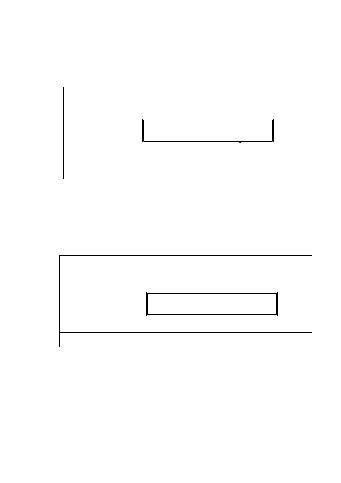
When you press “Enter” on this item, you get a confirmation dialog box with a message similar
to :
Standard CMOS Features
Advanced BIOS Features Load Fail-Safe Defaults
Advanced Chipset Features Load Optimized Defaults
Integrated Peripherals Set Supervisor Password
Power Management Setup Set User Password
PnP/ PCI Configurations Save & Exit Setup
PC Health Status Exit Without Saving
Esc : Quit
F10 : Save & Exit Setup
Pressing “Y” loads the BIOS default values for the most stable, minimal-performance system
operations.
3.12 LOAD OPTIMIZED DEFAULTS
When you press “Enter” on this item, you get a confirmation dialog box with a message similar
to :
Pressing “Y” loads the default values that are factory settings for optimal performance system
operations.
Standard CMOS Features
Advanced BIOS Features
Advanced Chipset Features
Integrated Peripherals
Power Management Setup
PnP/ PCI Configurations
PC Health Status
Esc
: Quit
F10
: Save & Exit Setup
Frequency/Voltage Control
Load Fail-Safe Defaults (Y/N) ? Y
á â àß
Load Fail-Safe Defaults
Load Optimized Defaults (Y/N) ? Y
á â àß
Frequency/Voltage Control
Load Fail-Safe Defaults
Load Optimized Defaults
Set Supervisor Password
Set User Password
Save & Exit Setup
Exit Without Saving
: Select Item
Load Optimized Defaults
: Select Item
Page: 42
Page 47

Page: 43
3.13 Set Supervisor/User Password
The “SUPERVISOR/USER PASSWORD” utility sets the password. The SBC is shipped with the
password disabled. If you want to change the password, you must first enter the current
password, then at the prompt -- enter your new password. The password is case sensitive, and
can be up to 8 alphanumeric characters. Press <Enter> after you have finished typing in the
password. At the next prompt, confirm the new password by re-typing it and pressing <Enter>
again. When you are done, the screen automatically reverts to the main screen. Remember
that when you use this feature, the “Security Option” line in BIOS FEATURES SETUP will
determine when entering the password will be required.
Standard CMOS Features
Advanced BIOS Features
Advanced Chipset Features Load Optimized Defaults
Integrated Peripherals Set Supervisor Password
Power Management Setup Set User Password
PnP/ PCI Configurations Save & Exit Setup
PC Health Status Exit Without Saving
Enter Password:
Esc : Quit
F10 : Save & Exit Setup
Change / Set / Disable Password
To disable the password, press the <Enter> key instead of entering a new password when
the “Enter Password” in the dialog box appears. A message will appear confirming that the
password is disabled.
If you have set both supervisor and user password, only the supervisor password allows you to
enter the BIOS SETUP PROGRAM.
Note : If you forget your password, the only way to solve this problem is to discharge the CMOS
memory by turning power off and placing a shunt on the S1 (open pad) for 5 seconds, then
removing the shunt.
3.14 SAVE & EXIT SETUP
Select this option and press the <Enter> key to save the new setting information in the CMOS
memory and continue with the booting process.
Standard CMOS Features
Advanced BIOS Features
Advanced Chipset Features Load Optimized Defaults
Integrated Peripherals Set Supervisor Password
Power Management Setup Set User Password
PnP/ PCI Configurations Save & Exit Setup
PC Health Status Exit Without Saving
Esc : Quit
F10 : Save & Exit Setup
Save to CMOS and EXIT (Y/N) ? Y
Save Data to CMOS.
Frequency/Voltage Control
Load Fail-Safe Defaults
á â àß
Frequency/Voltage Control
Load Fail-Safe Defaults
á â àß
: Select Item
: Select Item
Page 48
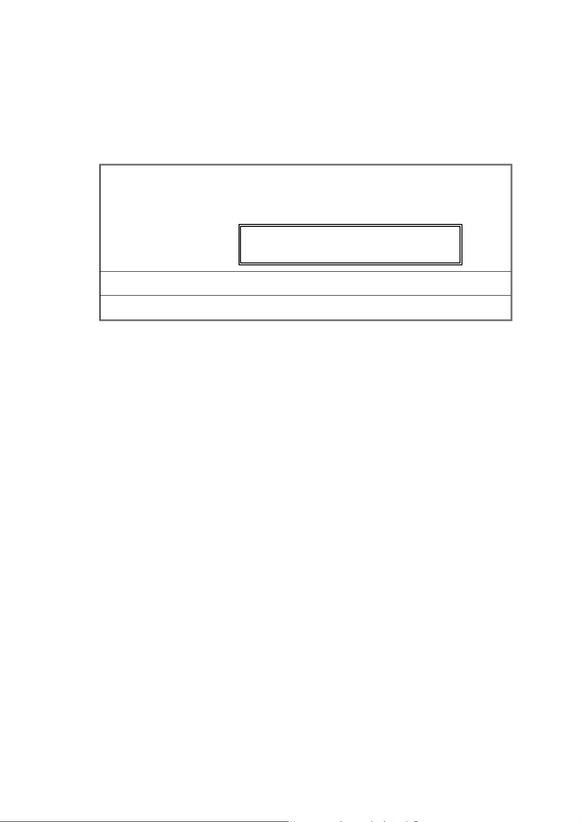
3.15 EXIT WITHOUT SAVING
Select this option and press the <Enter > key to exit the Setup Utility without recording any new
values or changing old ones
Standard CMOS Features
Advanced BIOS Features
Advanced Chipset Features Load Optimized Defaults
Integrated Peripherals Set Supervisor Password
Power Management Setup Set User Password
PnP/ PCI Configurations Save & Exit Setup
PC Health Status Exit Without Saving
Esc : Quit
F10 : Save & Exit Setup
Quit Without Saving (Y/N) ? N
á â àß
Abandon all Data
Frequency/Voltage Control
Load Fail-Safe Defaults
: Select Item
Page: 44
Page 49

Page: 45
CHAPTER 4. Drivers Support
4.1 Driver Support
4.1.1 CORE CHIP
For installing Microsoft Windows operating system (95/98/ME/NT/200), you will need some
device drivers. These drivers could be found in “EM-561 Series “directory on “Drivers CDROM”.
It is strongly recommended to use the driver provided instead of the ones supported by
Microsoft Windows system.
In “EM-561 Series” directory, there are three main sub-directories: Corechip, VGA and Ethernet.
Please refer to the explanation below for the explanation and installation.
Corechip:
Two sub-directories: “ide_exe” and “System”. You might found “it8888” sub-directory only in
some earlier version of “Driver CDROM” and it is not necessary to install this driver any more.)
Corechip/ide_exe
This directory contains Intel Ultra ATA Storage Driver 6.0. Please run the installing program
intelata603_multi.exe under Microsoft Windows systems.
Corechip/System
This directory contains Intel(R) Chipset Software Installation Utility. It will install to the target
system the Windows* INF files that outline to the operating system how the chipset
components will be configured. This is needed for the proper functioning of the following
features:
- Core PCI and ISA PnP Services
- AGP Support
- IDE/ATA33/ATA66 Storage Support
- USB Support
- Identification of Intel Chipset Components in Device Manager
Please refer to the readme.txt in directory Corechip/System/Disk1 before running the installing
program setup.exe
4.1.2 NETWORK
Ethernet
The directory contains Intel(R) PRO LAN Adapter drivers (release 4.1.1). There are drivers for
Microsoft Windows 95/98/ME/NT/2000, Novell NetWare Servers & Clients, Microsoft DOS and
IBM OS2. Please refer to readme.txt and relnotes.txt before installing the driver.
4.1.3 VGA
VGA: Sub-directories are listed below.
VGA/vga_linux:
The directory contains RPM for driving Intel 810 & 815 Chipset Family under Linux System.
Please refer to release_linux.pdf for installation information.
VGA/vga_nt4
The directory contains graphics drivers for Intel(R) 810/810E/815/815E Chipsets in Microsoft
Windows NT4.0. Please refer to readment4.txt first before running the auto-installing
program winnt4m60.exe.
Page 50
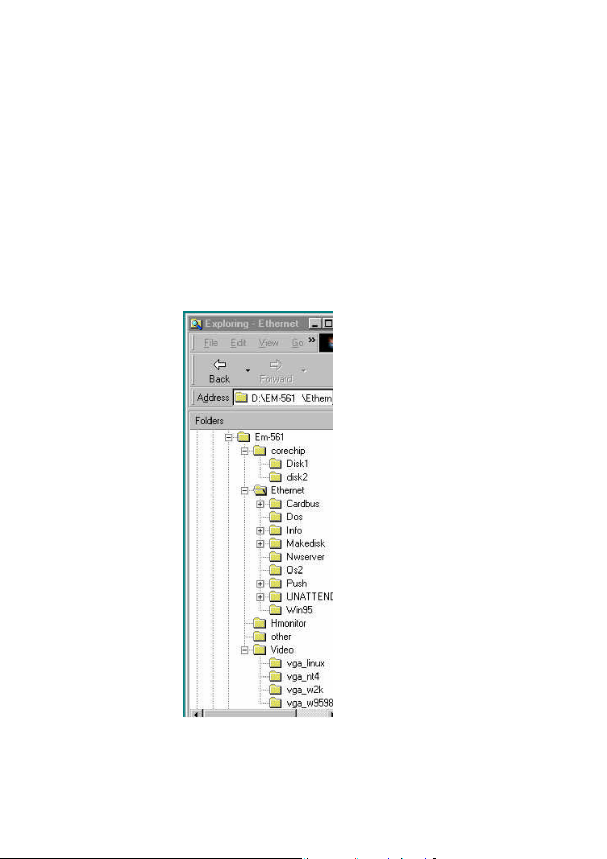
VGA/vga_w2k
The directory contains graphics drivers for Intel(R) 810/810E/815/815E Chipsets in Microsoft
Windows 2000. Please refer to readmewin2k.txt first before running the auto-installing
program win2km60.exe.
VGA/win9x
The directory contains graphics drivers for Intel(R) 810/810E/815/815E Chipsets in Microsoft
Windows 95/98/Millenium. Please refer to readme.txt first before running the auto-installing
program setup.exe.
4.1.4 HARDWARE MONITOR
Hmonitor
The directory contains graphics drivers for Intel(R) 810/810E/815/815E Chipsets. Please refer to
readme.txt before running the auto-installing program Install.exe.
4.2 DRIVER SUPPORT LIST
Page: 46
Page 51
Page: 47
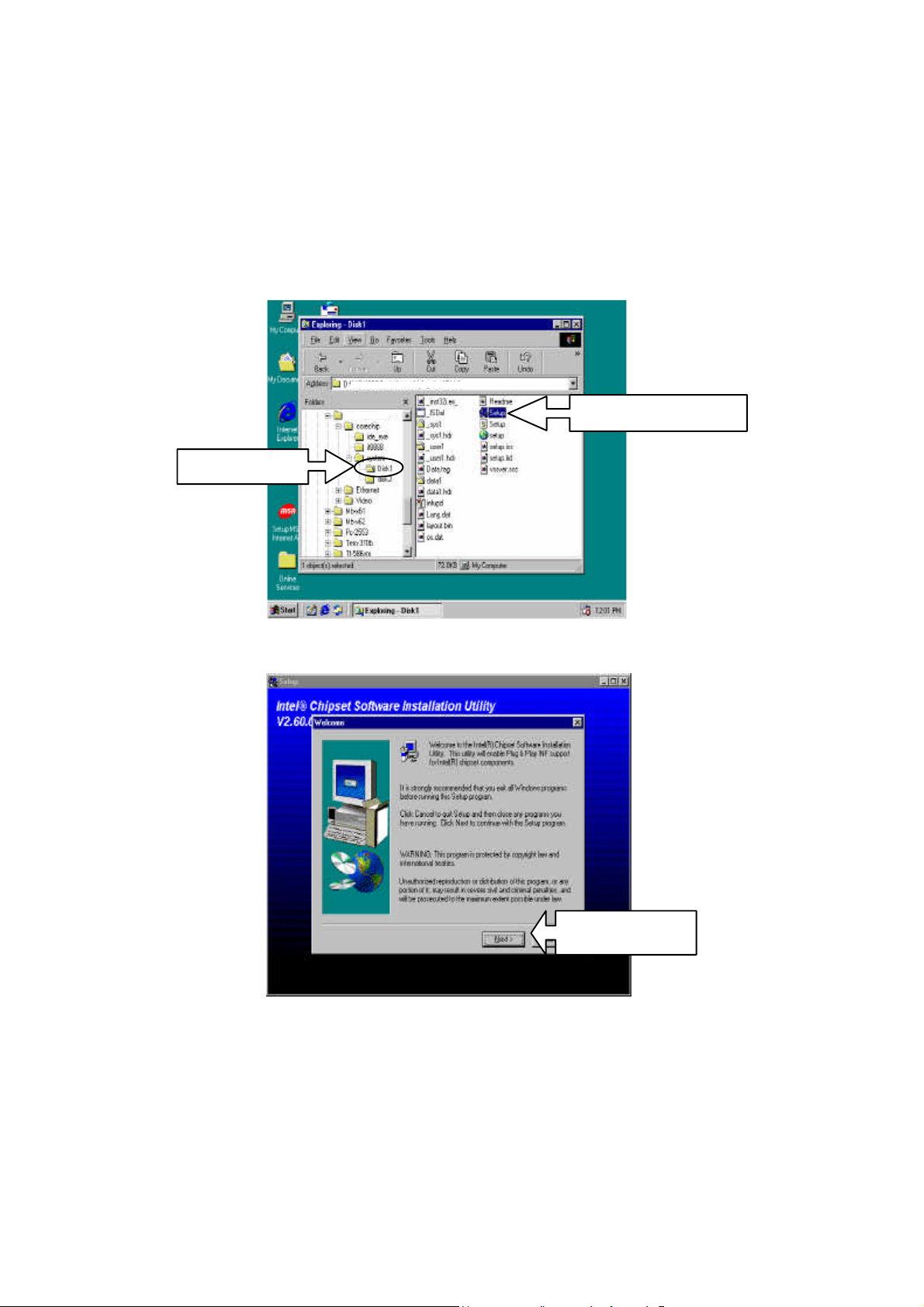
Click “Next”
1.Click Here
2. Double Click Here
4.3 DRIVER SETUP & INSTALLATION
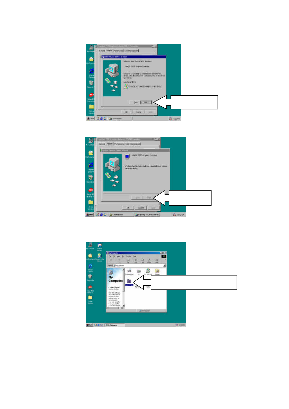
4.3.1 Intel 815 chipset Driver Setup
Setp 1. Run Driver CD-ROM
Setp 2. Directory: EM-561 Series / corechip / Disk1/ Setup.exe
Setp 3.
Page 52
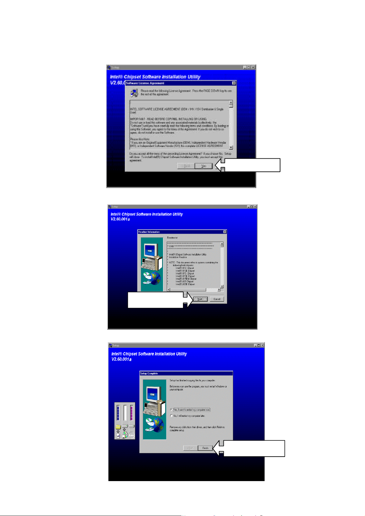
Click “Yes”
Click “Next”
Click “Finish”
Setp 4.
Setp 5.
Setp6
Page: 48
Page 53
Page: 49
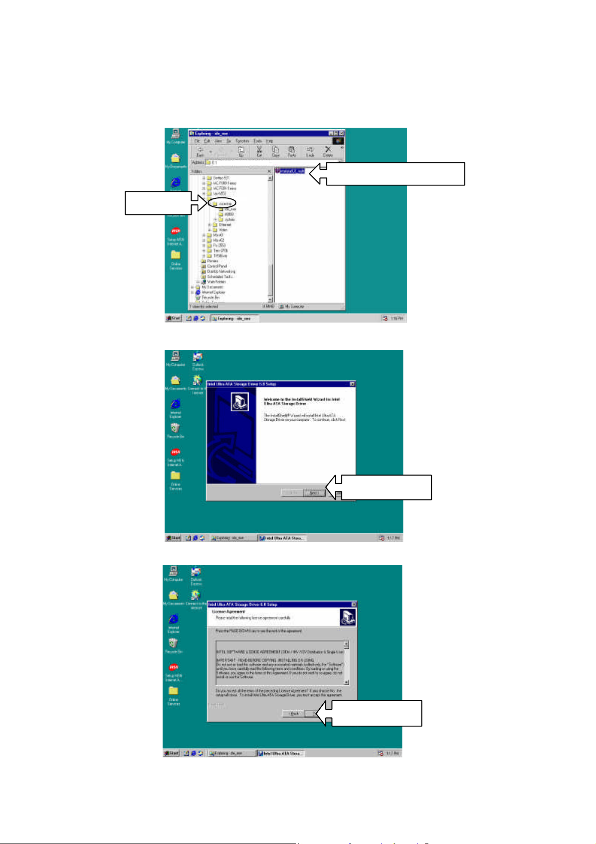
1. Click Here
Click “Next”
Click “Yes”
4.3.2 Intel Ultra ATA Storage Driver Install
Setp 1. Directory: EM-561 Series / corechip / intelata063_multi.exe
Setp 2.
Setp 3.
2. Double Click Here
Page 54
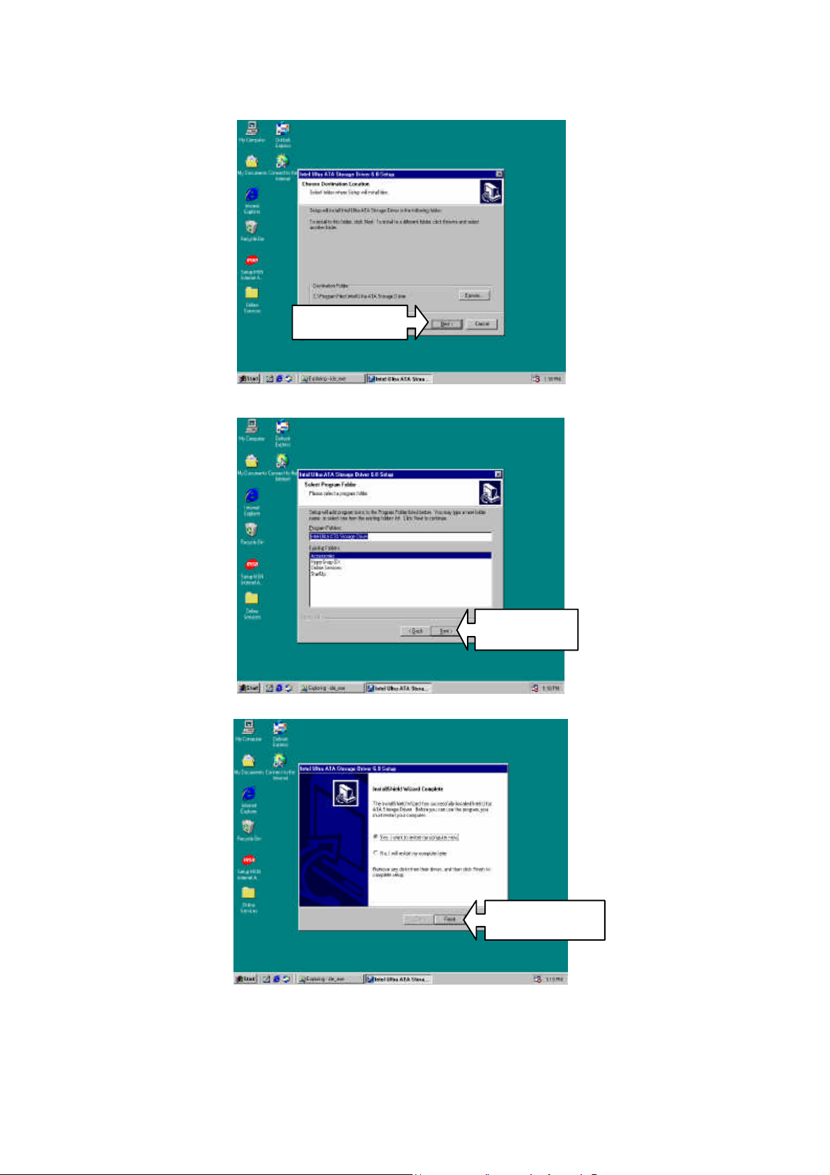
Click “Next”
Click “Next”
Click “Finish”
Setp 4.
Setp 5.
Setp 6.
Page: 50
Page 55
Page: 51
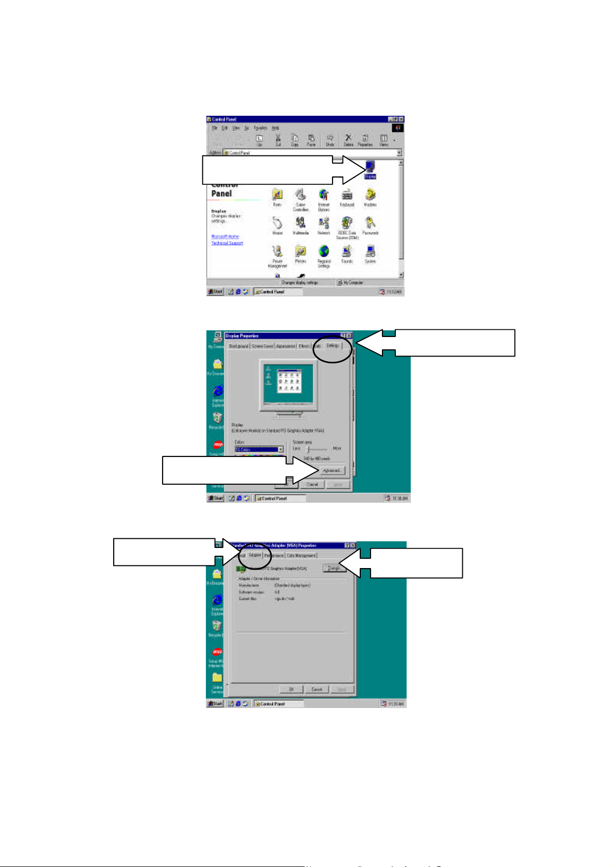
Double Click “Display”
1.Select “Settings”
Click “Advanced”
Click “Change”
Select “Adapter”
4.3.3 VGA Driver Install
Step 1
Step 2.
Setp 3.
Page 56
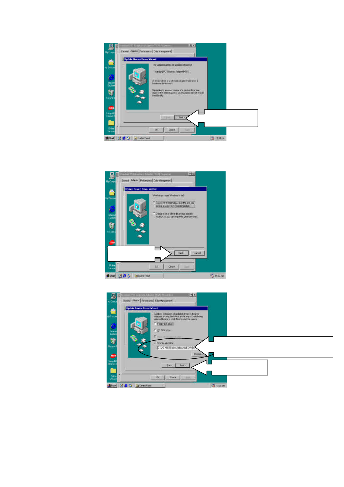
Click “Next”
Click “Next”
Click “Next”
2. Directory: EM-561 Series/Video/xx
Step 4.
Step 5.
Step 6.
1. Put Driver CD-ROM
Page: 52
Page 57
Page: 53
Click “Finish”
Click “Next”
Double Click “Control Panel”
Step 7.
Step 8.
4.3.4 LAN Driver Install
Setp 1.
Page 58
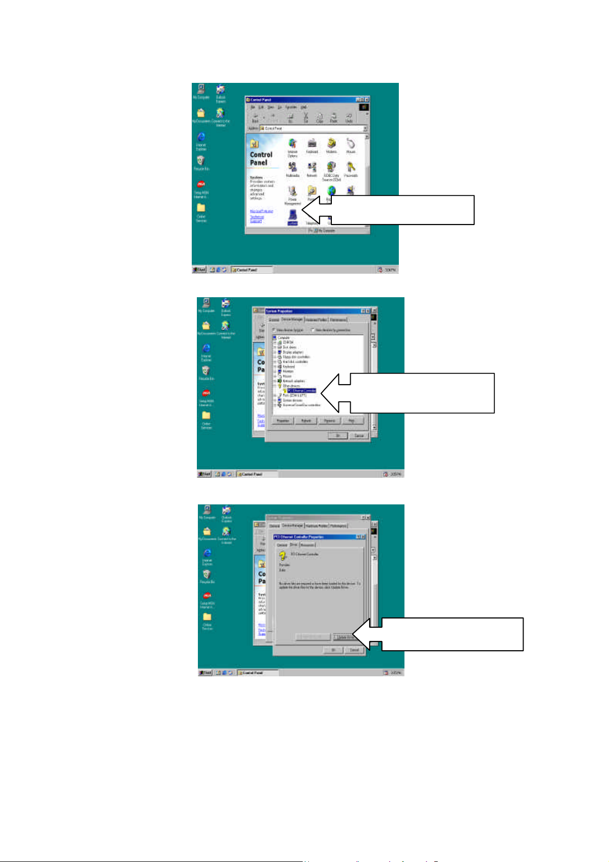
Click “Update Driver”
Setp 2.
Double Click “System”
Setp 3.
Double Click
Setp 4.
Page: 54
Page 59
Page: 55
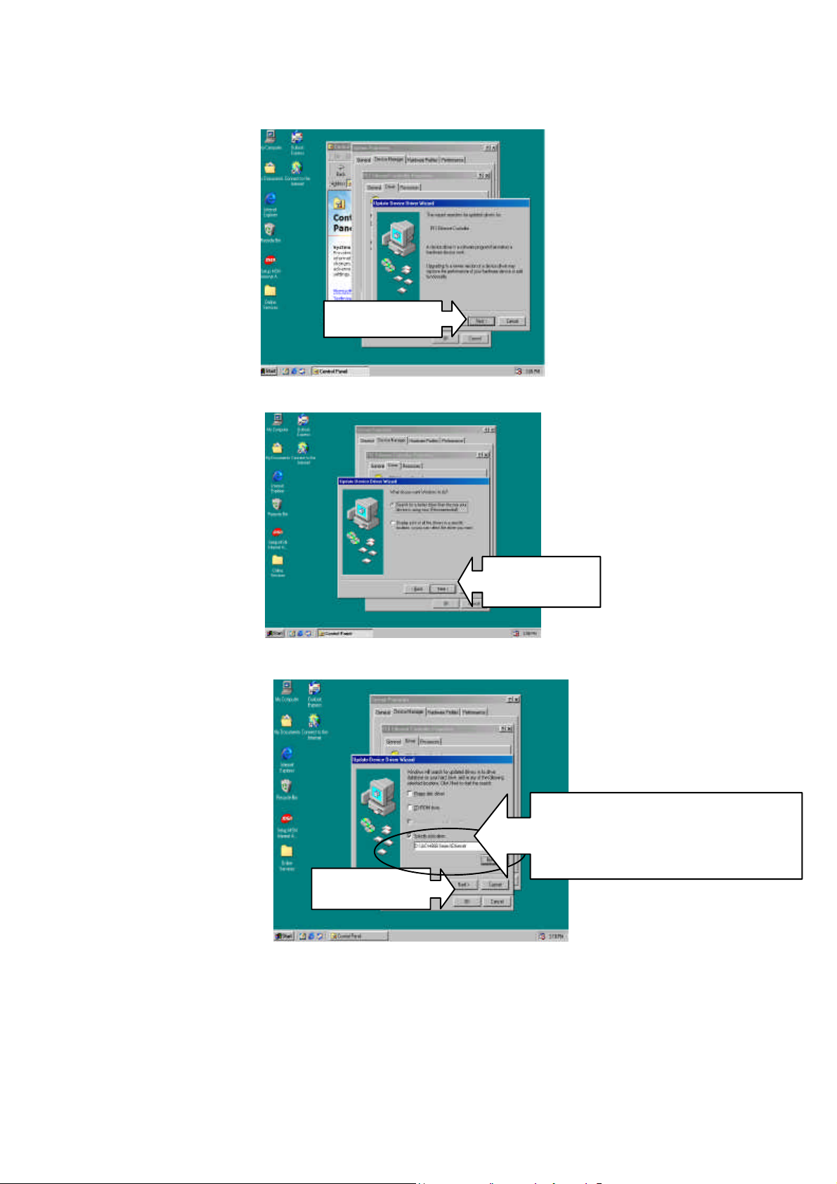
Click “Next”
Click “Next”
Click “Next”
Setp 5.
Setp 6.
Setp7.
1. Select “Specify a location”
2. Put Driver CD-ROM
3. Find LAN Driver file.
Page 60
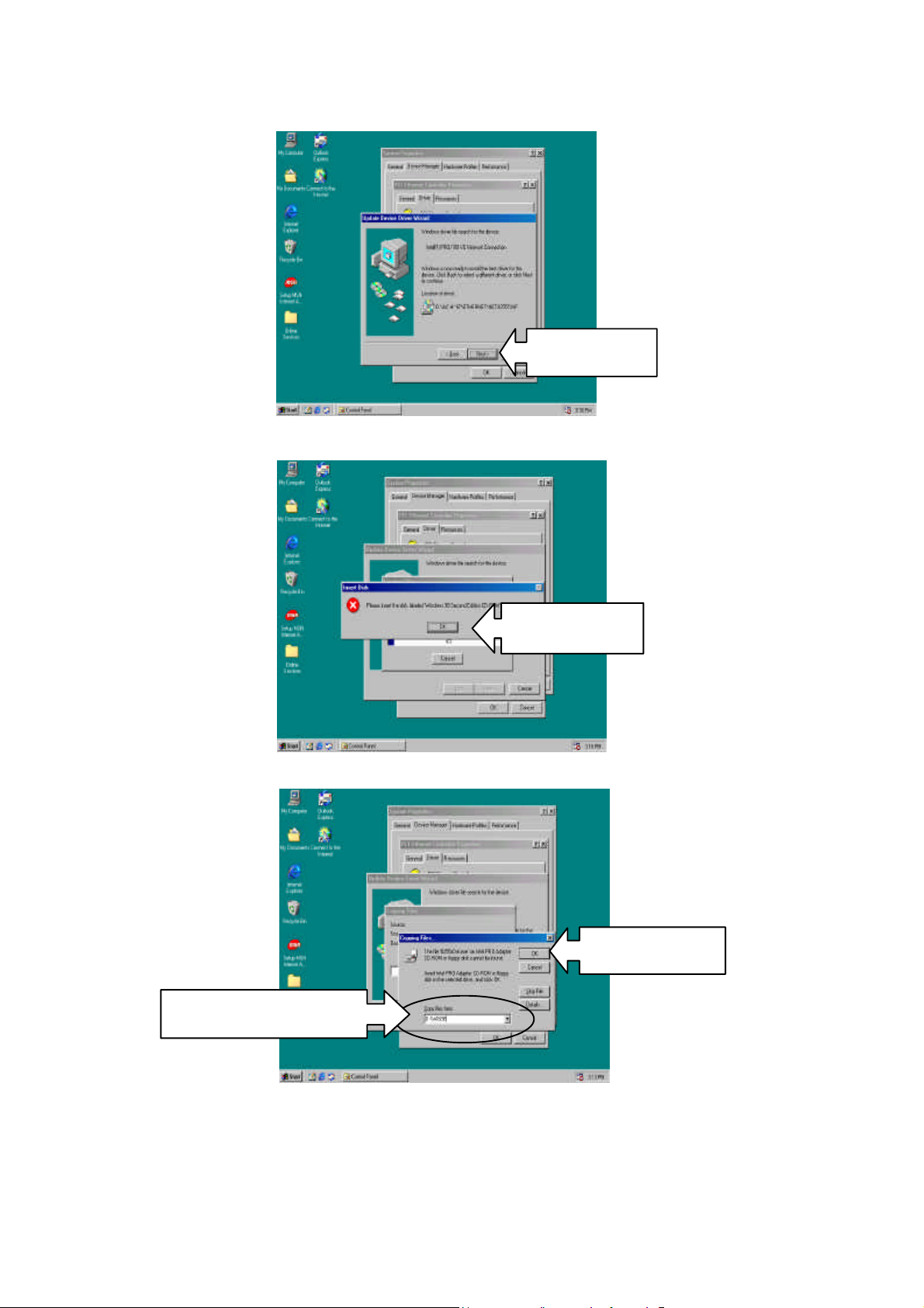
Click “Next”
2.Click “OK”
Click “OK”
1.Put win98 CD-ROM
Setp 8.
Setp 9.
Setp 10.
Page: 56
Page 61
Page: 57
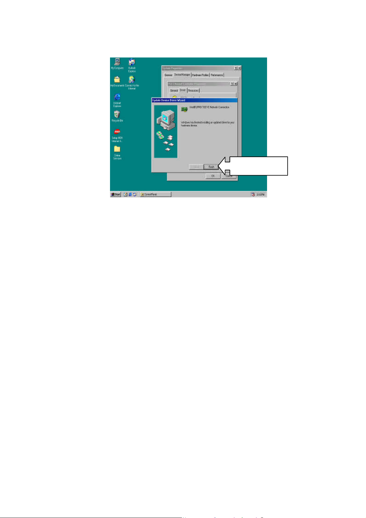
Click “Finish”
Setp 11.
Page 62

APPENDIX A. How to use watch-dog timer
To use the watch-dog timer :
Step 1. Enable and retrigger the Watch-Dog timer : Output port 443H
Step 2. Disable : Output port 441H
EX.1: For DOS
Execute the DEBUG.EXE file under DOS, Then key-in O443. The system will
reboot automatically according to the time-out you set.
Enable Disable
C:\DOS> DEBUG C:\DOS> DEBUG
O 443 0~F O 441 0~F
EX.2: For assemble Language
Enable :
:
:
MOV DX, 443H
OUT DX , AL
:
:
Disable :
:
:
MOV DX, 441H
OUT DX , AL
:
Page 63
Terms and Conditions
Date:1997.10.20
Warranty Policy
1. All products are warranted against defects in materials and workmanship on a period
of two years from the date of purchase by the customer.
2. The buyer will bear the return freight charges for goods that are returned for repair
within the warranty period whereas manufacturer will bear the other way after repair.
3. The buyer will pay for repair (for the replaced materials plus service time) and
transportation charges (both ways) for items after the expiration of the warranty
period.
4. If the RMA Service Request Form does not meet the stated requirement as listed on
“RMA Service “ , RMA goods will be returned at the customer expense.
5. The following conditions are excluded from this warranty:
A. Improper or inadequate maintenance by the customer.
B. Unauthorized modification or misuse.
C. Operation outside of the environmental specifications for the product.
RMA Service
1. Request a RMA# :
Complete and fax to Supplier the “RMA Request Form” to obtain a RMA number.
2. Shipping:
A. The customer is requested to fill up the problem code as listed . If none of the
code is selected, please write the symptom description on the remark.
B. Ship the defective units with freight prepaid.
C. Mark the RMA # clearly on the box.
D. Shipping damage as a result of inadequate packing is the customer‘s
responsibility.
E. Use the original packing materials whenever possible .
3. All RMA# are valid for 30 days only:
When RMA goods are received after valid RMA# period , the goods will be rejected.
Page 64

RMA Service Request Form
When requesting RMA service, please fill out this “RMA Service Request Form”.
Without this form your RMA will be REJECTED!!!
RMA No:
Company: Contact Person:
Phone No. Purchased Date:
Fax No.: Applied Date:
Return Shipping Address:
Shipping by: □Air Freight □Sea □Express: □Others:
Reasons to Return: □ Repair(Please include failure details) □
Testing Purpose
Item Model Name Serial Number Configuration
Item
Problem Code Failure Status
*Problem Code:
01:D.O.A.
02: Second Time R.M.A.
03: CMOS Data Lost
04: FDC Fail
05: HDC Fail
06: Bad Slot
Request Party
Authorized Signatures / Date Authorized Signatures / Date
07: BIOS Problem
08: Keyboard Controller Fail
09: Cache RMA Problem
10: Memory Socket Bad
11: Hang Up Software
12: Out Look Damage
13: SCSI
14: LPT Port
15: PS2
16: LAN
17: COM Port
18: Watchdog Timer
Confirmed By Supplier
19: DIO
20: Buzzer
21: Shut Down
22: Panel Fail
23: CRT Fail
24: Others (Pls specify)
 Loading...