

Page 1

AP-545V
Single Board Computer with VGA
for ZIF Socket 7 Processor
Page 2

COPYRIGHT
This document is a copyright of the original manufacturer, 1998. The original manufacturer reserves
the right to make improvements to the product(s) described in this manual at any time without notice.
This manual may not, in whole or in part, be photocopied, reproduced, transcribed, translated, or
transmitted in whatever form without the written consent of the manufacturer, except for copies
retained by the purchaser for backup purposes. All rights are reserved.
©
TRADEMARKS
Pentiumâ is a registered trademark of Intel Corporation.
The following are trademarks or registered trademarks of their respective companies: IBM, Intel, AMD,
Cyrix, Award, AMI, Microsoft, Windows, Windows NT, Novell, SCO, PC/104, PICMG, ALI, UMC,
SMC, Winbond. Products mentioned in this manual are mentioned for identification purposes only.
All names of products or services appearing in this manual are the trademarks or registered
trademarks of their respective organizations and companies.
ã Copyright 1998
Ver. No. 1.1
LEI-UM-AP545V0-002
Date : 3.22.2000
Page 3

TABLE OF CONTENTS
CHAPTER 1 INTRODUCTION 1
1.1 SPECIFICATIONS 2
1.2 PACKING CHECK LIST 3
CHAPTER 2 JUMPER SETTINGS AND CONNECTORS 4
2.1 BOARD OUTLINE OF AP-545V 4
2.2 CPU INSTALLING AND UPGRADING 5
2.3 JUMPER SETTING OVERVIEW 5
2.4 JUMPER LOCATION FOR AP-545V 6
2.5 JUMPER SETTINGS SUMMARY FOR AP-545V 7
2.6 JUMPER SETTINGS FOR AP-545V 8
2.7 I/O CONNECTORS LOCATION FOR AP-545V 14
2.8 I/O CONNECTORS SUMMARY FOR AP-545V 15
2.9 SETTING STATUS INDICATORS AND CONTROL 16
CONNECTORS
2.10 I/O CONNECTORS DESCRIPTION 17
CHAPTER 3 AMI BIOS SETUP 25
3.1 RUNNING AMI BIOS 25
3.2 AMI BIOS HIFLEX SETUP UTILITY 26
3.3 STANDARD CMOS SETUP 27
3.4 ADVANCED CMOS SETUP 31
3.5 ADVANCED CHIPSET SETUP 36
3.6 POWER MANAGEMENT SETUP 38
3.7 PCI PLUG AND PLAY SETUP 41
3.8 PERIPHERAL SETUP 45
3.9 CHANGE SUPERVISOR/USER PASSWORD 47
3.10 UTILITY 49
3.11 BIOS DEFAULTS 49
Page 4

Page 5

TABLE OF CONTENTS
APPENDIX A HOW TO USE WATCH-DOG TIMER 50
APPENDIX B TECHNICAL REFERENCE 51
APPENDIX C LANNER PCI PIGGYBACK MODULE 53
INSTALLATION
GLOSSARY
TERMS AND CONDITIONS
RMA SERVICE REQUEST FORM
Page 6

Page 7

AP-545V/1
CHAPTER 1.
INTRODUCTION
The AP-545V is a half-size ISA single board computer for Socket 7 processor that is using the SIS’s
BGA chipset SiS5598 that support the Ultra DMA-33 for faster hard drive, VGA and USB function.
For boosting operation, this motivated card also supports sockets for a Flash Disk and one DIMM
memory module. It offers the function of an industrial computer on a single board with on-board 2nd
level cache RAM of 512KB for maximum performance.
The AP-545V is built with patent PCI piggyback expansion bus that is simply upgraded by changing
one card from another without replacing the whole system. It provides the primarily elements for
building an IBM PC/AT compatible computer for a wide variety of applications with system integration.
The AP-545V is fully compatible with the IBM PC/AT which means virtually all the software written for
the IBM PC/AT will run on the AP-545V SBC.
Other on-board features include two serial ports (one each of RS-232 and RS-232/422/485), one
multi-mode parallel (ECP/EPP/SPP) port, a floppy drive controller and a keyboard interface and a
PS/2 mouse interface. The built-in one high speed PCI IDE controller supports both PIO and bus
master modes. Up to two IDE devices can be connected, including large hard disks, CD-ROM
drives, tape backup drives and other IDE devices. Its 6-layer printed circuit board combines with
noise-tolerant and low power consumption CMOS technology applied on the board makes AP-545V
able to withstand any harsh industrial environments very well.
Page 8

INTRODUCTION
AP-545V/2
1.1 SPECIFICATIONS
o Processor : For ZIF Socket 7 Processor
Intel PentiumÒ & MMX, AMD K5 & K6, Cyrix 6x86 &
M2 CPU
o Chipset : SiS 5598 Chipset, Winbond I/O chipset compatible
o System Memory : One 168-pin DIMM socket up to 128MB SDRAM
o Cache Memory : On-board 512KB Pipelined Burst Synchronous cache
o BIOS : 256KB AMI License BIOS
o Flash Memory Disk : Reserved socket for DiskOnChip from M-System
support up to 72 MB Flash Memory Disk
o VGA Controller : VGA on chipset SiS 5598, on-board 2MB shared
memory
o IDE Drive Interface : One PCI IDE port, support up to two IDE devices and
Ultra DMA-33
o Floppy Drive Interface : One FDD port, support up to two floppy devices
o Serial Port : Two COM ports, one RS-232 and one RS-
232/422/485 serial ports
o Parallel Port : One multi-mode parallel port (SPP/EPP/ECP)
o Bus Interface : Optional ISA bus
o RTC Battery : Dallas RTC battery or compatible
o DMA : 8 DMA channels
o Interrupts : 16 levels of hardware interrupts
o PS/2 Mouse Connector : On-board 6-pin Mini-Din PS/2 Mouse connector
o Keyboard Connector : On-board 5-pin header and 6-pin Mini-Din connectors
o Expansion Bus : On-board patent PCI piggyback expansion bus
o Watchdog Timer : 8 level time-out intervals (0.5/1/2/4/8/16/32/64 sec.)
o Universal Serial Bus : Support 2 USB ports
o IR Interface : Support one IrDA header
o Operating Temperature : 0°C~55°C (32°F~132°F)
o Humidity : 10%~90% RH
o Dimensions : 185 mm X 122 mm (7
o Net weight : 250 g (0.517 pounds)
1
/4” X 45/6” inches)
Page 9
INTRODUCTION
AP-545V/3
1.2 PACKING CHECK LIST
Before you begin to install your card, please make sure that you received the following materials as
listed below:
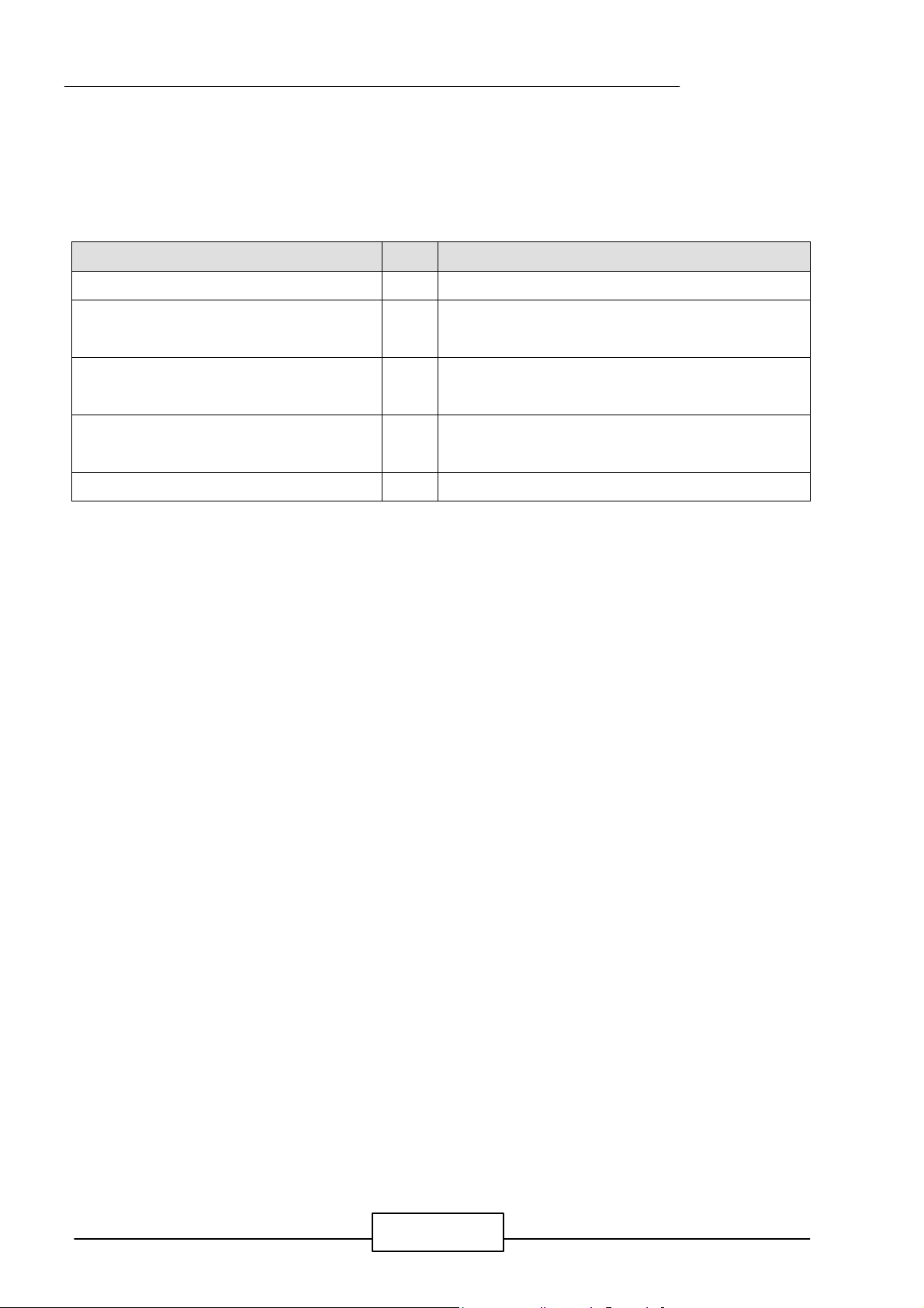
Item Qty Remark
AP-545V Single Board Computer 1 pc.
Keyboard adapter cable 1 set 6-pin AT keyboard connector to 5-pin PS/2 keyboard
connector
IDE/Floppy cable 1 pc. 40-pin standard header to 40-pin standard header
34-pin standard header to 34-pin standard header
Printer port cable 1 set 26-pin female flat connector t header to 25-pin male
D-Sub connector
User‘s manual 1 pc. AP-545V
Page 10
AP-545V/4
AP-545V
IR1
JP5
PRT1
USBC1
KCN1
CHAPTER 2.
JUMPER SETTINGS AND CONNECTORS
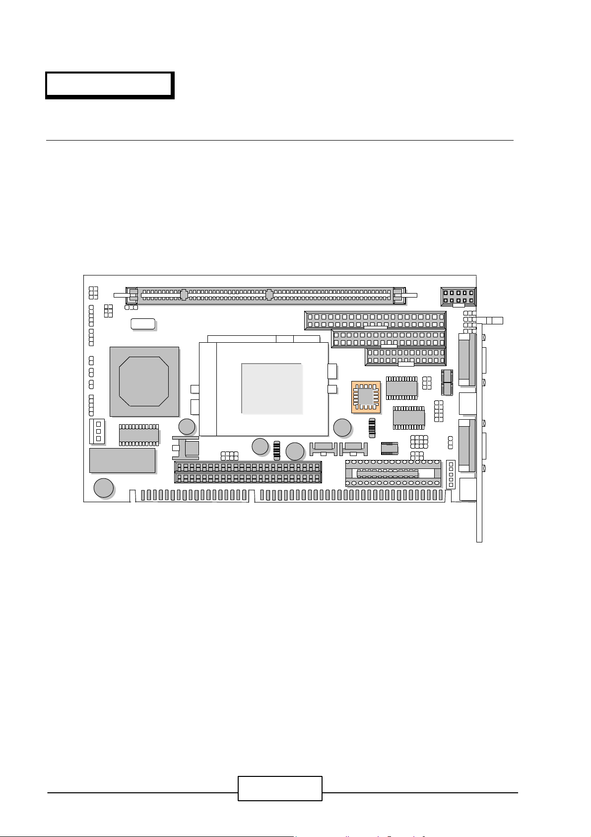
2.1 BOARD OUTLINE OF AP-545V
The Figure below shows the jumpers and connectors location on the AP-545V:
SiS
5598
l
CPU
Page 11
JUMPER SETTING AND CONNECTORS
AP-545V/5
2.2 CPU INSTALLING AND UPGRADING
To upgrade to a higher power Pentium CPU, simply remove the old CPU and install to a new one; be
sure to set the jumpers for the new CPU type and speed.
WARNING!
Disconnect the power cord from your system when you intend to work on it or you plan
to open the chassis of your IPC. Do not make connections when the power is turned
on as sensitive electronic components can be damaged by the sudden rush of power.
Please only allow experienced electronics technicians to do this job.
STATIC ELECTRICITY PRECAUTION!
Caution! Computer components are very sensitive to damage from static electric
discharge. Always ground yourself to remove static charge build-up before touching
the boards in the computer. Use a grounding wrist strap at all time. Place all
electronic components on the anti-static pad for static-dissipation or in a
static-shielded bag when they are not in the chassis.
2.3 JUMPER SETTING OVERVIEW
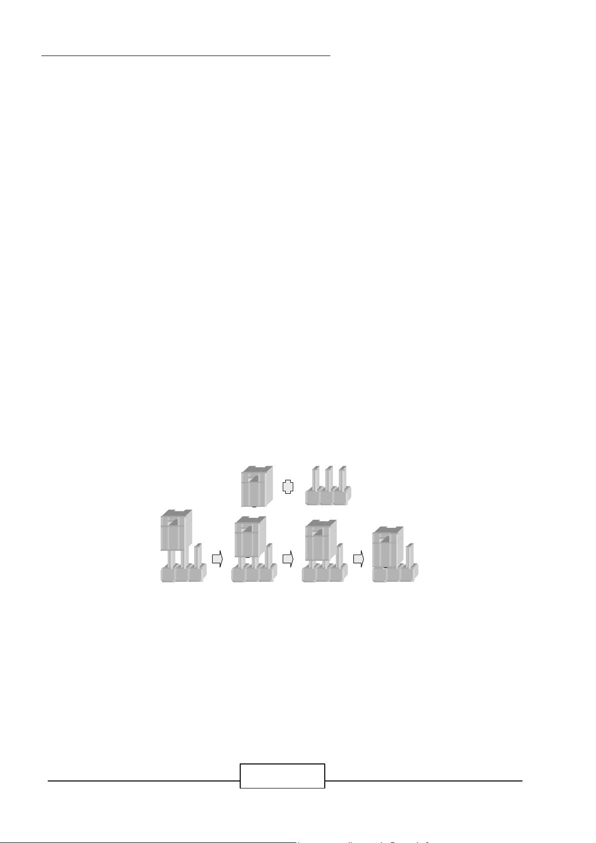
In order to select the operation modes of your system, configure and set the jumpers on the your SBC
to match the need of your application. To set a jumper, a black plastic cap containing metal contacts
is placed over the jumper pins as designated by the required configuration as listed in this section. A
jumper is said to be “ on ” or “ 1-2 ” when the black cap has been placed on two of its pins, as show
in the figure below:
A pair of needle-nose pliers is recommended when working with jumpers. If you have any doubts
about the best hardware configuration for your application, contact your local sales representative
before you make any changes. In general, you simply need a standard cable to make most
connections.
Page 12
JUMPER SETTING AND CONNECTORS
AP-545V/6
AP-545V
JP12
JP5
JP7
JP10
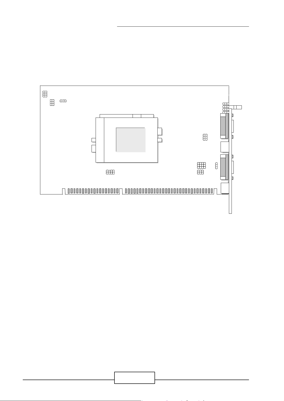
2.4 JUMPER LOCATION FOR AP-545V
CPU
Page 13

AP-545V/7
2.5 JUMPER SETTINGS SUMMARY FOR AP-545V
JUMPERS
LOCATION FUNCTION
JP1 Select Internal CPU Clock Ratio
JP2 Select External CPU Clock
JP3 Select External VGA Function
JP4 ~ JP8 Select Serial Port#2 Type
JP10 Select Watch-Dog Time Out Period
JP11 M-System Address
JP12 Select Watch-Dog Function
JP13 Select Vcore Voltage
JUMPER SETTING AND CONNECTORS
Page 14
JUMPER SETTING AND CONNECTORS
AP-545V/8
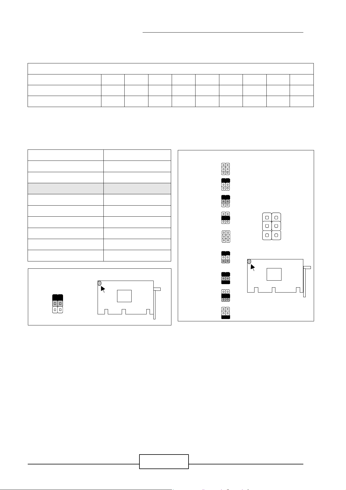
2.6 JUMPER SETTINGS FOR AP-545V
CPU Speed Reference Table
CPU Speed (MHz) 75 90 100 120 133 150 166 200 233
Clock setting 50 60 66.6 60 66.6 60 66.6 66.6 66.6
Frequency ratio 1.5 1.5 1.5 2 2 2.5 2.5 3 3.5
l JP1 : Select Internal CPU Clock Ratio
Clock Ratio JP1
1.5 X OFF
2.0 X 1-2
2.5 X ( Default ) 1-2 , 3-4
3.0 X 3-4
3.5 X OFF
4.0 X 1-2 , 5-6
4.5 X 1-2 , 3-4 , 5-6
5.0 X 3-4 , 5-6
5.5 X 5-6
Default :
JP1
1
3
5
2
4
6
1.5X
2.0X
2.5X
3.0X
3.5X
4.0X
4.5X
5.0X
5.5X
1
3
5
JP1
2
4
6
JP1
1
3
5
JP1
2
4
6
Page 15
AP-545V/9
Default :
Default :
1
JP2
50MHz
60MHz
66.6MHz
75MHz
83.3MHz
5 2 6
JP2
JP2
Enable
JP3
Disable
1
2
JP3
JP3
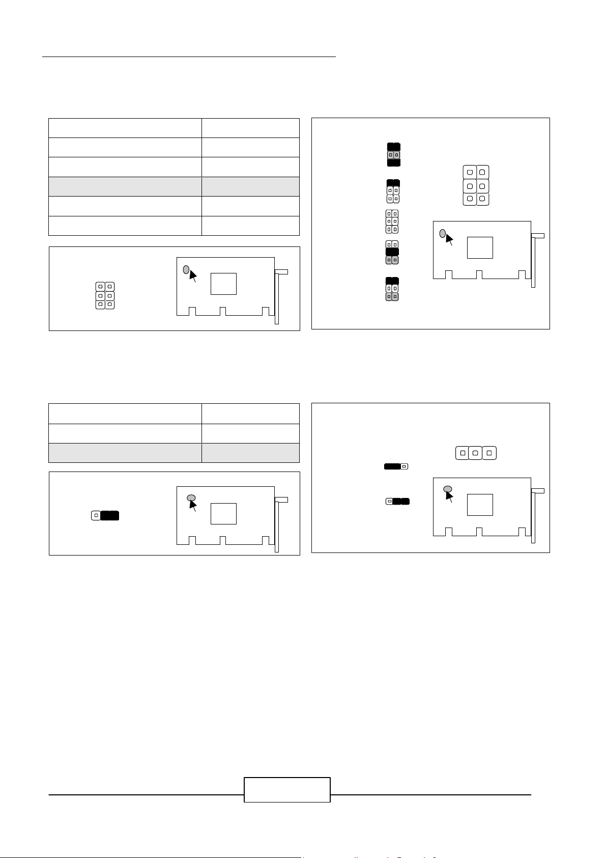
l JP2 : Select External CPU Clock
External CPU Clock JP2
50 MHz 1-2 , 3-4 , 5-6
JUMPER SETTING AND CONNECTORS
60 MHz 1-2
66.6 MHz (Default ) OFF
75 MHz 3-4 , 5-6
83.3 MHz 1-2 , 3-4
l JP3 : Select Internal VGA Function
JP2
1
5
2
6
VGA Chips JP3
Disable 1-2
Enable ( Default ) 2-3
1
5
1
2
6
3
JP3
1
3
Page 16
JUMPER SETTING AND CONNECTORS
AP-545V/10
Default :
5 6 1 1 1 1 3 3 3 3
RS-232
RS-422
RS-485
1 5 2
6
JP8
JP7
JP5
JP4
JP6
1 1 1 1 3 3 3
3
JP7
JP8
JP5
JP4
JP6
JP4
JP8
JP5
JP6
JP7
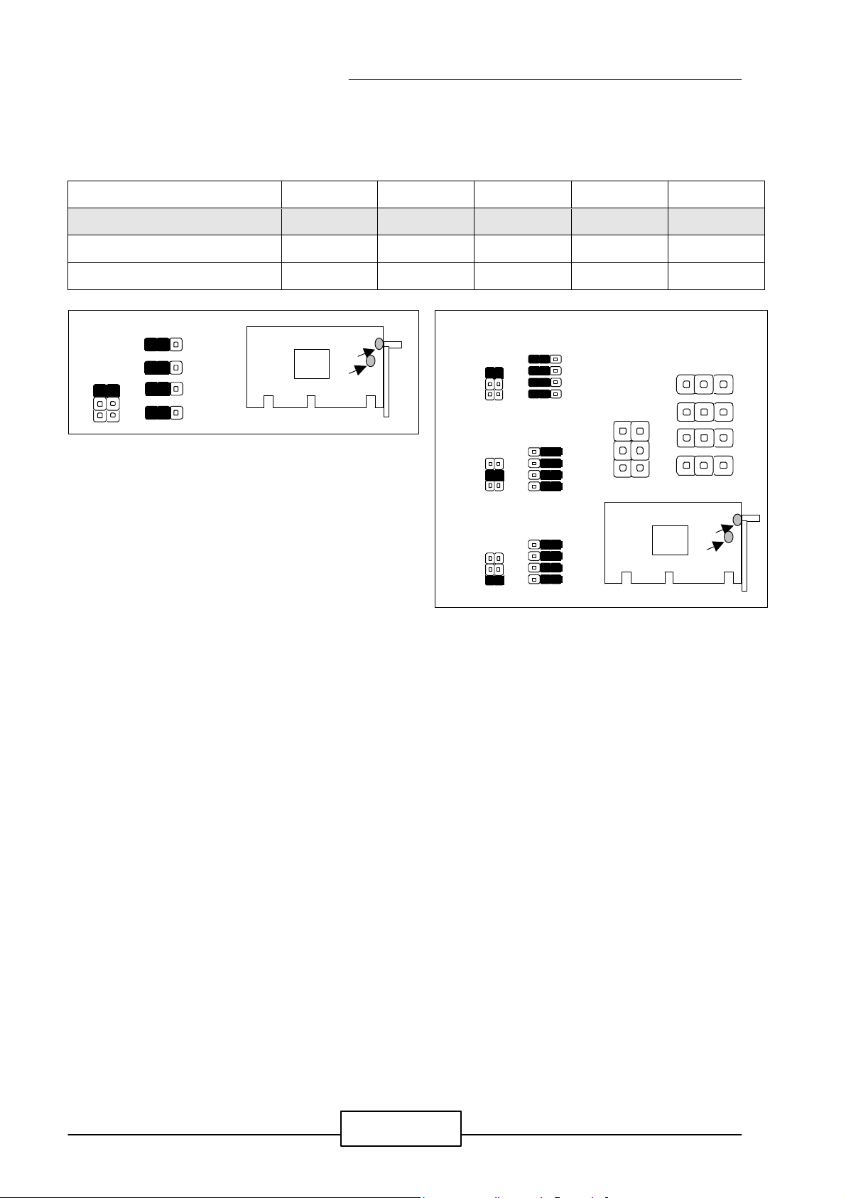
l JP4~JP8 : Select Serial Port#2 Type
COM2 Type JP4 JP5 JP6 JP7 JP8
RS-232 ( Default ) 1-2 1-2 1-2 1-2 1-2
RS-422 2-3 2-3 2-3 2-3 3-4
RS-485 2-3 2-3 2-3 2-3 5-6
JP8
1
2
JP4
JP5
JP6
JP7
1
2
5
6
Page 17
AP-545V/11
Default :
H
3
2
1 4
Default :
6
2
1
5
JP10
1 SEC
L
H
1
4
2
3
L
H
1 2 3
4
JP10
C8000~CFFFF
D0000~D7FFF
D8000~DFFFF
2 1 6
5
JP11
JP11
JP11
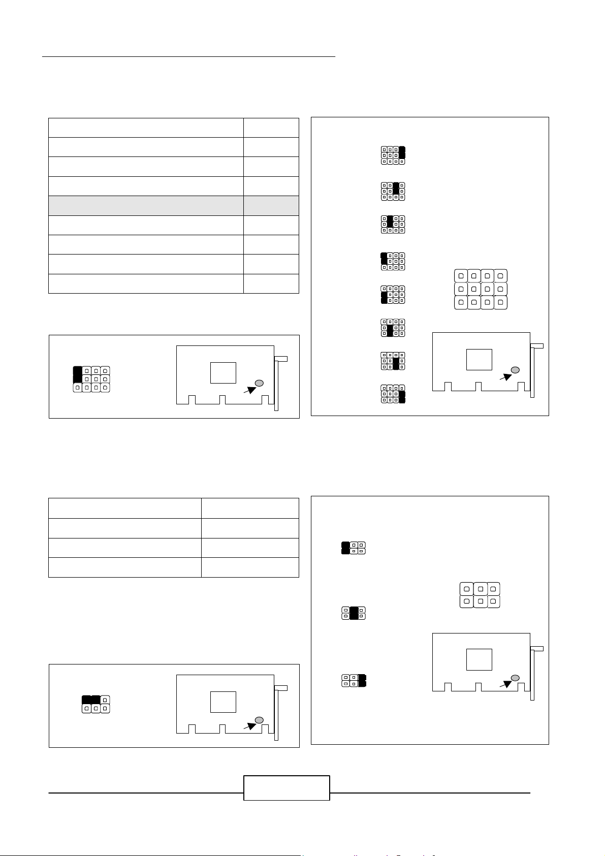
l JP10 : Select Watch-Dog Time Out Period
Time Out Period JP10
JUMPER SETTING AND CONNECTORS
0.5 sec 1L
1 sec 2L
2 sec 3L
4 sec (Default ) 4L
8 sec 4H
16 sec 3H
32 sec 2H
64 sec 1H
L
JP10
0.5 SEC
2 SEC
JP10
4 SEC
8 SEC
16 SEC
32 SEC
64 SEC
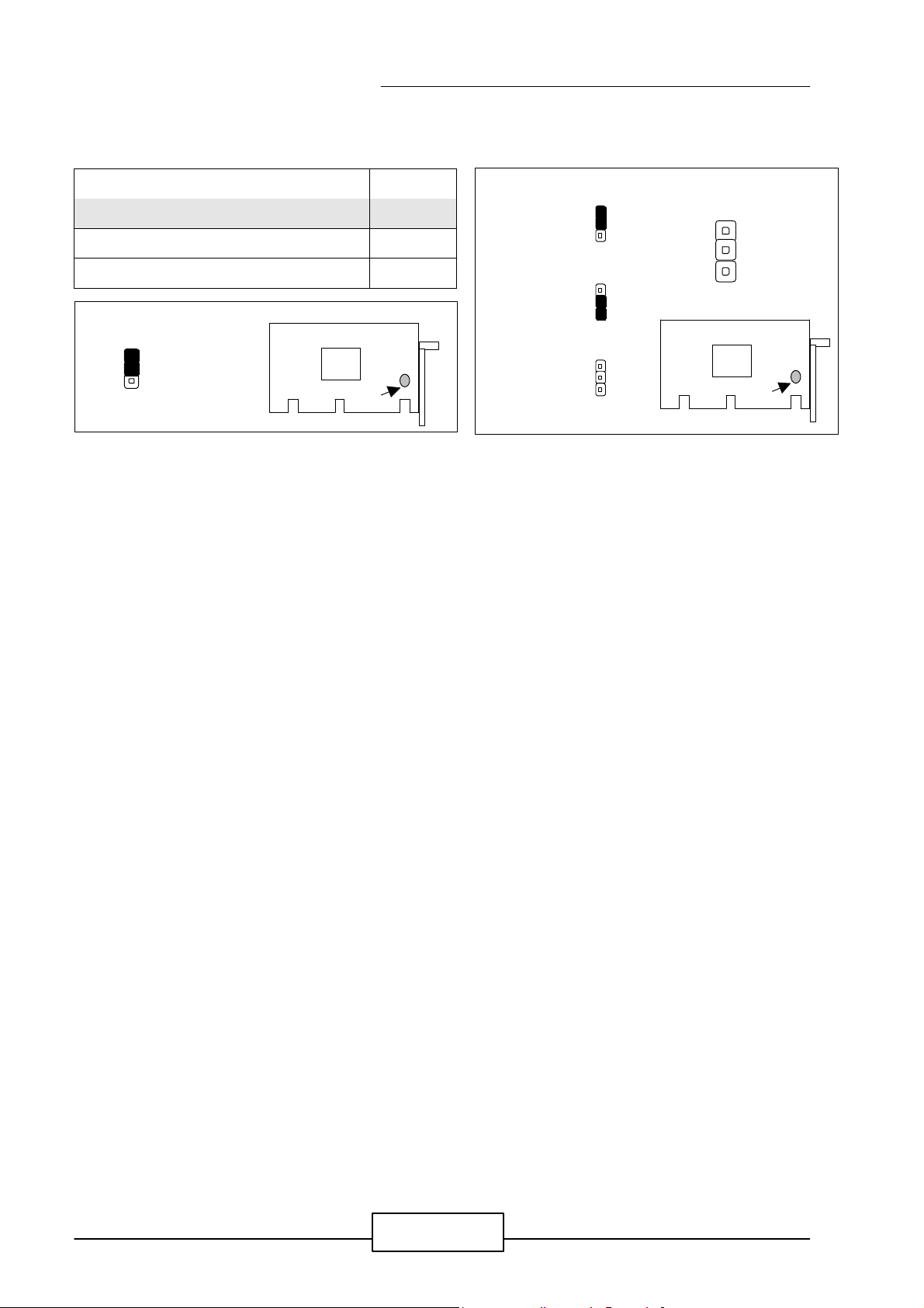
l JP11 : M-System Address
M-System Address JP11
C8000~CFFFF 1-2
D0000~D7FFF 3-4
D8000~DFFFF 5-6
Note : Spare Jumper at 2-4;M-System address
C8000 is already occupied by VGA BIOS
;therefore only D0000 and D8000
addresses are free.
JP11
2
1
6
5
Page 18
JUMPER SETTING AND CONNECTORS
AP-545V/12
Default :
JP12
1
3
JP12
JP12
l JP12 : Select Watch-Dog Function
Function JP12
Active By Reset System ( Default ) 1-2
Active By NMI System 2-3
Disable Watch-Dog OFF
JP12
1
3
Active By Reset
System
Active By NMI
System
Disable
Watch-Dog
1
3
Page 19
AP-545V/13
Default :
7 5 3 1
8 6 4 2
7 5 3 1
8 6 4 2
7 5 3 1
8 6 4 2
2.0V
2.3V
2.4V
2.5V
2.6V
2.7V
2.8V
2.9V
3.0V
3.1V
3.2V
3.3V
3.4V
3.5V
JP13
JP13
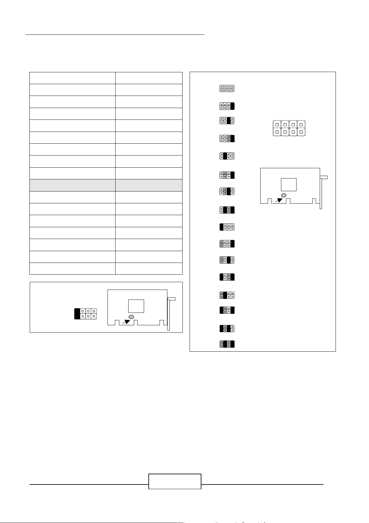
l JP13 : Select Vcore Voltage
Vcore Voltage JP13
2.0 V OFF
JUMPER SETTING AND CONNECTORS
2.1 V 1-2
2.1V
JP13
2.2 V 3-4
2.3 V 1-2 , 3-4
2.2V
2.4 V 5-6
2.5 V 1-2 , 5-6
2.6 V 3-4 , 5-6
2.7 V 1-2 , 3-4 , 5-6
2.8 V ( Default ) 7-8
2.9 V 1-2 , 7-8
3.0 V 3-4 , 7-8
3.1 V 1-2 , 3-4 , 7-8
3.2 V 5-6 , 7-8
3.3 V 1-2 , 5-6 , 7-8
3.4 V 3-4 , 5-6 , 7-8
3.5 V 1-2 , 3-4 , 5-6 , 7-8
JP13
Note : Spare Jumper at 2-4
Page 20
JUMPER SETTING AND CONNECTORS
AP-545V/14
AP-545V
IR1
PRT1
USBC1
KCN1
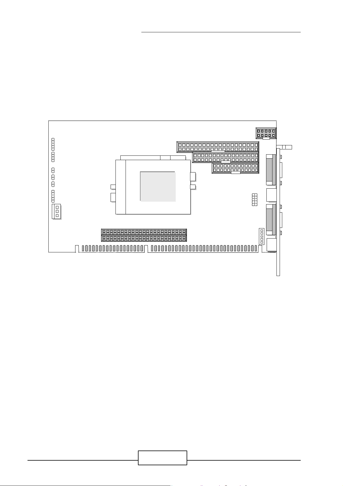
2.7 I/O CONNECTOR LOCATION FOR AP-545V
CPU
Page 21

AP-545V/15
2.8 I/O CONNECTOR SUMMARY FOR AP-545V
CONNECTOR FUNCTION
JP9 ACPI LED
J1 Power LED & Keyboard Lock Connector
J2 Ext. Speaker Connector
J3 IDE Active LED Connector
J4 Reset Connector
FAN1 FAN Connector
VGA1 VGA Monitor Connector
IDE1 PCI IDE Interface Connector
IR1 IrDA Connector
KCN1 5 Pin Keyboard Connector (Header)
PKB1 PS/2 Keyboard Connector (Mini-Din)
JUMPER SETTING AND CONNECTORS
PMS1 PS/2 Mouse Connector (Mini-Din)
USBC1
COM1 Serial Part #1 Connector (D-Sub)
COM2 Serial Part #2 Connector
PRT1 Parallel Port Connector
FDC1 Floppy Interface Connector
PC1、PC2
USB#1、USB#2 Interface Connector
PCI Bus Connector
Page 22
JUMPER SETTING AND CONNECTORS
AP-545V/16
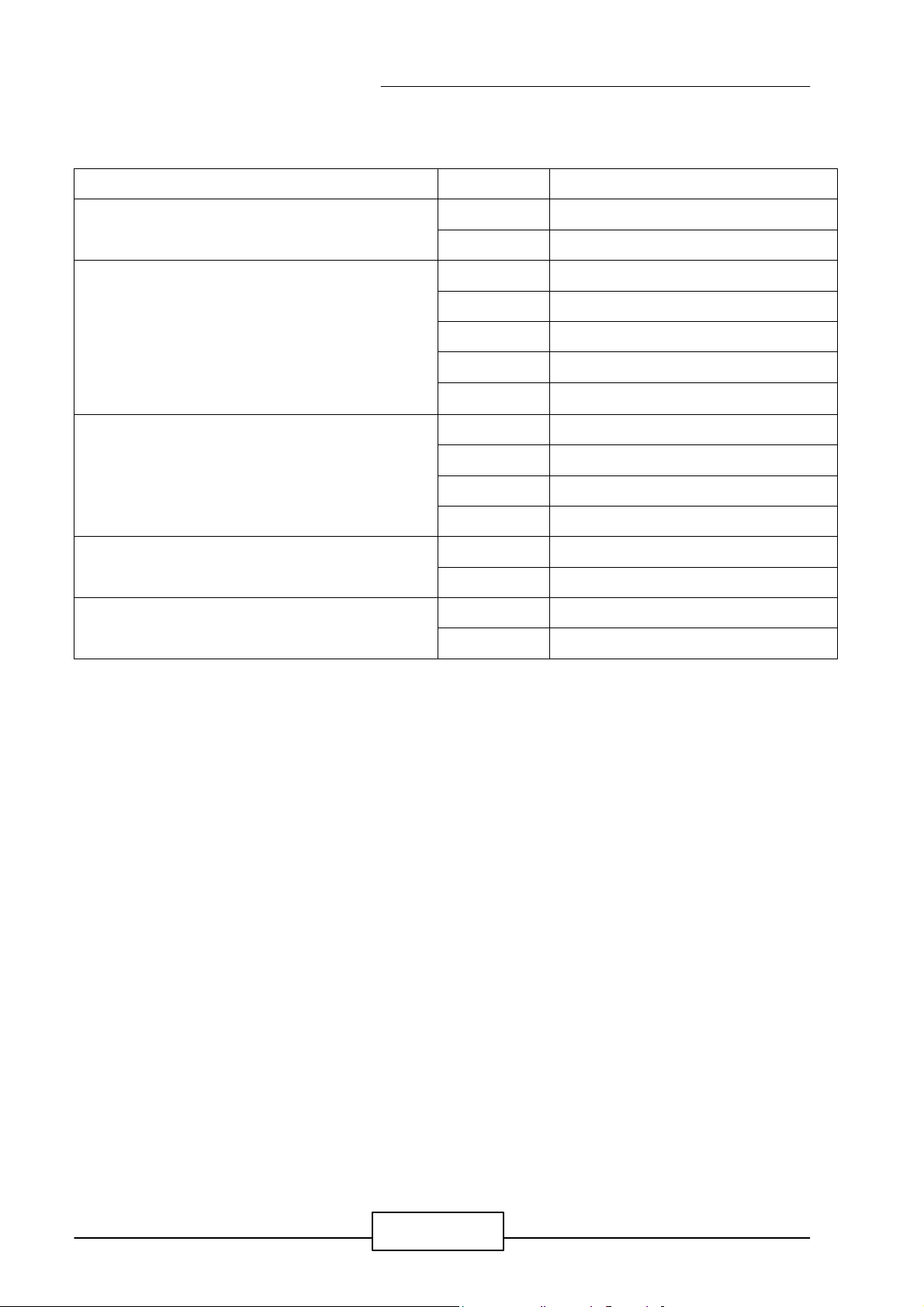
2.9 SYSTEM STATUS INDICATE AND CONTROL CONNECTORS
CONNECTOR PIN NO. DESCRIPTION
JP9 : ACPI LED 1 VCC3
J1 : Power LED & Keyboard Connector 1 Power LED VCC
2 NC
3 GND
4 Keyboard Lock Signal
J2 : Ext. Speaker Connector 1 Speak Out Signal
4 VCC
J3 : IDE Active LED Connector 1 VCC
2 IDE Active Signal
J4 : Reset Connector 1 Reset Input Signal
2 GND
2 ACPI Signal
5 GND
2 NC
3 NC
Page 23
AP-545V/17
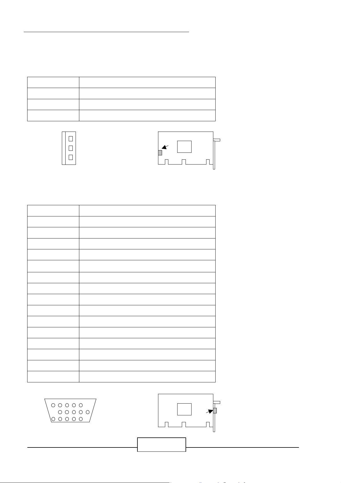
FAN1
1 3 VGA1
5
1
6
10
11
15
2.10 I/O CONNECTORS DESCRIPTION
l FAN1 : FAN Connector
PIN NO. DESCRIPTION
1 Ground
2 +12V
3 NC
JUMPER SETTING AND CONNECTORS
l VGA1 : VGA Monitor Connector
PIN NO. DESCRIPTION
1 Red Color Signal
2 Green Color Signal
3 Blue Color Signal
4 NC
5 Ground
6 Ground
7 Ground
8 Ground
9 VCC
10 Ground
11 NC
12 DDC-Data
13 H-Sync.
14 V-Sync.
15 DDC-Clock
Page 24
JUMPER SETTING AND CONNECTORS
AP-545V/18
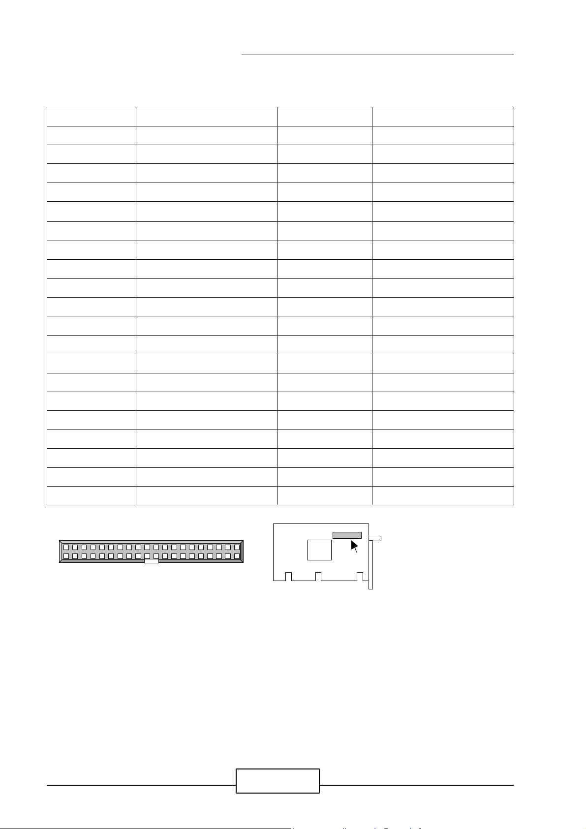
IDE1
2 1 39
40
l IDE1 : PCI IDE Interface Connector
PIN NO. DESCRIPTION PIN NO. DESCRIPTION
1 Reset # 2 Ground
3 Data 7 4 Data 8
5 Data 6 6 Data 9
7 Data 5 8 Data 10
9 Data 4 10 Data 11
11 Data 3 12 Data 12
13 Data 2 14 Data 13
15 Data 1 16 Data 14
17 Data 0 18 Data 15
19 Ground 20 NC
21 DMA REQ# 22 Ground
23 IOW# 24 Ground
25 IOR# 26 Ground
27 IOCHRDY 28 Ground
29 DMA ACK# 30 Ground
31 IRQ# 32 Ground
33 SA1 34 NC
35 SA0 36 SA2
37 HDC CS0# 38 HDC CS1#
39 HDD Active 40 Ground
Page 25
AP-545V/19
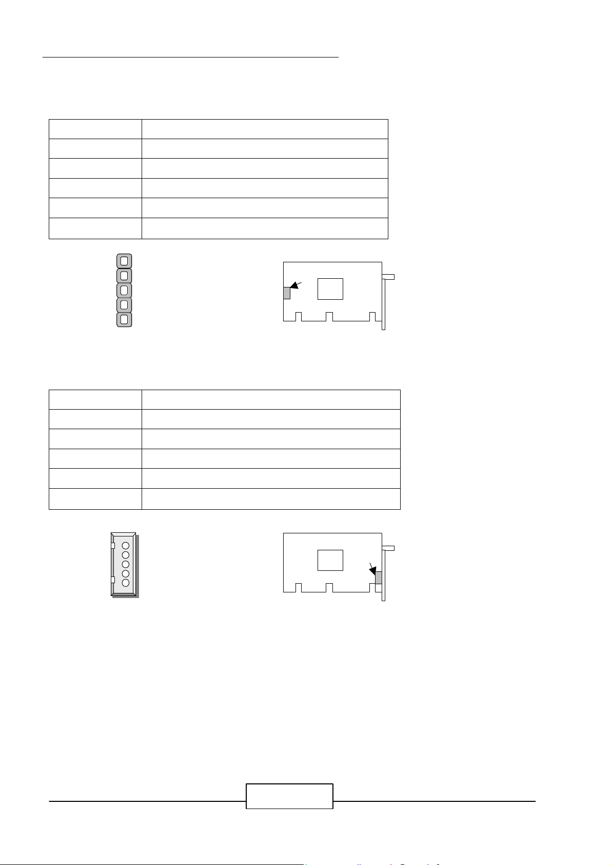
IR1
1 5 5 1 KCN1
l IR1 : IrDa Connector
PIN NO. DESCRIPTION
1 VCC
2 NC
3 IR_RX
4 Ground
5 IR_TX
JUMPER SETTING AND CONNECTORS
l KCN1 : 5 PIN Keyboard Connector ( Header )
PIN NO. DESCRIPTION
1 Keyboard Clock
2 Keyboard Data
3 NC
4 Ground
5 VCC
Page 26
JUMPER SETTING AND CONNECTORS
AP-545V/20
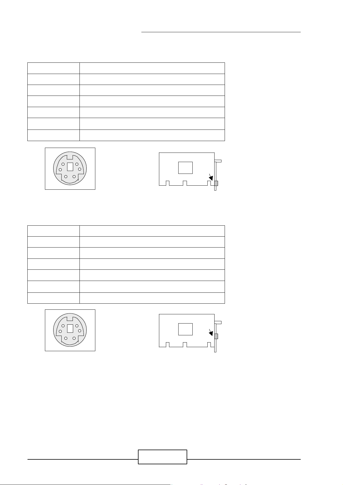
PKB1
PMS1
l PKB1 : PS/2 Keyboard Connector ( Mini Din )
PIN NO. DESCRIPTION
1 PS/2 Keyboard Data
2 NC
3 Ground
4 VCC
5 PS/2 Keyboard Clock
6 NC
l PMS1 : PS/2 Mouse Connector ( Mini Din )
PIN NO. DESCRIPTION
1 PS/2 Mouse Data
2 NC
3 Ground
4 VCC
5 PS/2 Mouse Clock
6 NC
Page 27
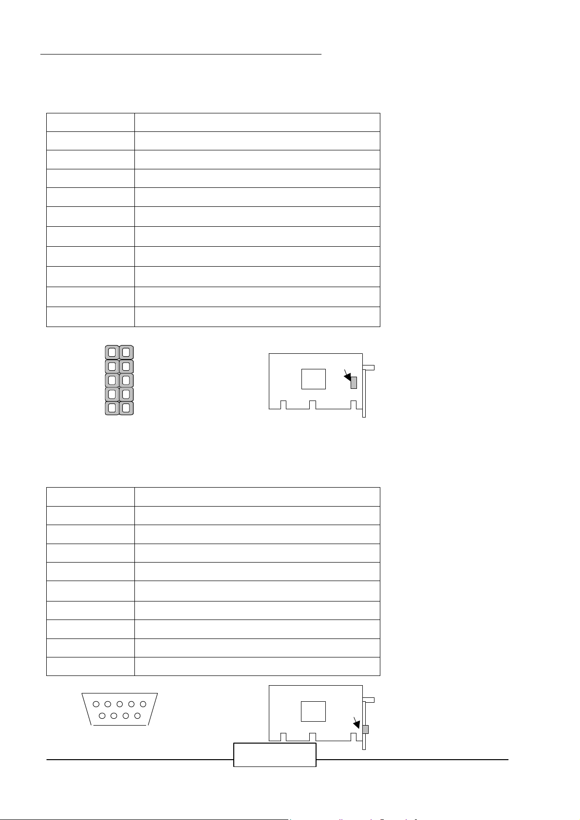
AP-545V/21
USBC1
5 1 1 5 COM1
1 5 9
6
l USBC1 : USB#1、#2 Interface Connector
PIN NO. DESCRIPTION
1 VCC
2 USB D0-
3 USB D0+
4 Ground
5 Ground
6 VCC
7 USB D1-
8 USB D1+
9 Ground
10 Ground
JUMPER SETTING AND CONNECTORS
l COM1 : Serial Port#1 Connector ( D-Sub )
PIN NO. DESCRIPTION
1 Data Carrier Detect ( DCD# )
2 Receive Data ( RXD )
3 Transmit Data ( TXD )
4 Data Terminal Ready ( DTR# )
5 Ground ( GND )
6 Data Set Ready ( DSR# )
7 Request To Send ( RTS# )
8 Clear To Send ( CTS# )
9 Ring Indicator ( RI# )
Page 28
JUMPER SETTING AND CONNECTORS
AP-545V/22
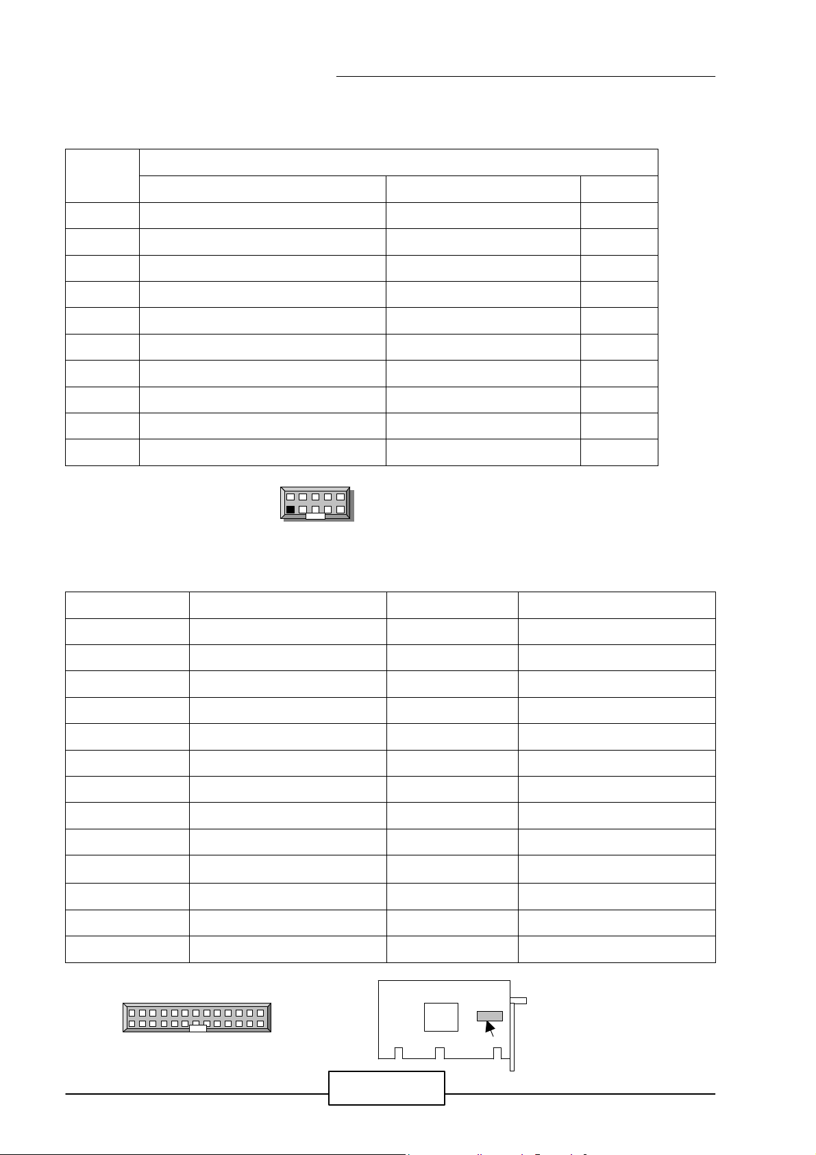
1 2 9
10
COM2
l COM2 : Serial Port #2 Connector ( Header )
PIN NO.
DESCRIPTION
RS-232 RS-422 RS-485
1 Data Carrier Detect (DCDB #) Transmit Data– (TXD-) Data 2 Receive Data (RXDB) Transmit Data+ (TXD+) Data +
3 Transmit Data (TXDB) Receive Data+ (RXD+) NC
4 Data Terminal Ready (DTRB #) Receive Data- (RXD-) NC
5 Ground NC NC
6 Data Set Ready (DSRB #) NC NC
7 Request To Send (RTSB #) NC NC
8 Clear To Send (CTSB #) NC NC
9 Ring Indicator (RIB #) NC NC
10 NC NC NC
l PRT1 : Parallel Port Connector
PIN NO. DESCRIPTION PIN NO. DESCRIPTION
1 Strobe # 2 Data 0
3 Data 1 4 Data 2
5 Data 3 6 Data 4
7 Data 5 8 Data 6
9 Data 7 10 Acknowledge #
11 Busy 12 Paper Empty
13 Printer Select 14 Auto Form Feed #
15 Error # 16 Initialize #
17 Printer Select IN # 18 Ground
19 Ground 20 Ground
21 Ground 22 Ground
23 Ground 24 Ground
25 Ground 26 NC
26 2
1
PRT1
25
Page 29
JUMPER SETTING AND CONNECTORS
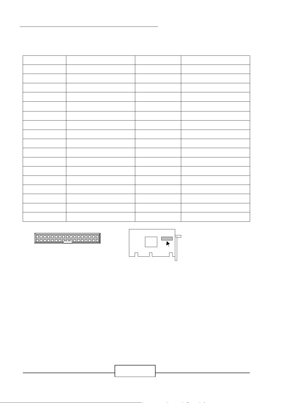
l FDC1 : Floppy Interface Connector
PIN NO. DESCRIPTION PIN NO. DESCRIPTION
1 Ground 2 Density Select
3 Ground 4 NC
5 Ground 6 NC
7 Ground 8 Index #
9 Ground 10 Motor Enable A#
11 Ground 12 Drive Select B#
13 Ground 14 Drive Select A#
15 Ground 16 Motor Enable B#
17 Ground 18 Direction #
19 Ground 20 Step #
21 Ground 22 Write Data #
23 Ground 24 Write Gate #
25 Ground 26 Track 0#
27 Ground 28 Write Protect #
29 NC 30 Read Data #
31 Ground 32 Head Side Select #
33 NC 34 Disk Change #
34 2
1
FDC1
33
Page 30
JUMPER SETTING AND CONNECTORS
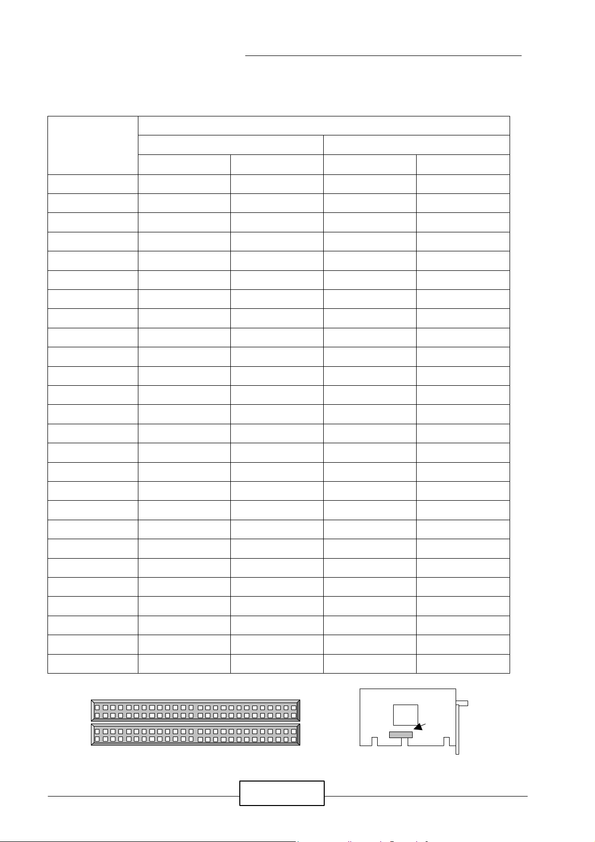
l PC1 , PC2 : PCI Bus Connector
PIN NO.
DESCRIPTION
PC1 PC2
A B A B
1 NC -12V STOP# C/BE2#
2 +12V NC SDONE IRDY#
3 PGNT1# Ground VCC DEVSEL#
4 VCC PREQ1# SBO# Ground
5 PINT0# VCC Ground PLOCK#
6 PINT2# VCC PAR PERR#
7 VCC PINT1# AD15 SERR#
8 PCIRST# PINT3# AD13 C/BE1#
9 VCC PREQ2# Ground AD14
10 PGNT0# Ground AD11 Ground
11 Ground Clock1 AD9 AD12
12 PGNT2# Ground C/BE0# AD10
13 AD30 PREQ3# VCC VCC
14 AD28 PREQ0# AD6 AD8
15 AD26 VCC AD4 AD7
16 AD24 AD31 Ground Ground
17 PGNT3# AD29 Ground AD5
18 Ground Ground AD2 AD3
19 AD22 AD27 AD0 Ground
20 AD20 AD25 VCC AD1
21 AD18 C/BE3# REQ64# VCC
22 AD16 AD23 NC ACK64#
23 FRAME# AD21 NC VCC
24 Ground Ground Ground NC
25 TRDY# AD19 Clock2 Ground
26 Clock0 AD17 Ground Clock3
52
51
52
51
PC1
PC2
B
2
1
A
B 2
1
A
Page 31

CHAPTER 3.
AMI BIOS SETUP
The AMI‘s ROM BIOS provides a built-in Setup program that allows user to modify the basic system
configuration and settings. The modified data will be stored in a battery-backed CMOS RAM so that
these data will be retained even when the power is turned off. In general, the information saved in the
CMOS RAM stay unchanged unless there is configuration change in the system, such as hard drive
replacement or new equipment is installed. AMI is a registered trademark of the American
Megatrends, Inc.
3.1 R
The Setup Utility is stored in the BIOS ROM. When the power of the computer system is turned on,
a screen message appears to give you an opportunity to call up the Setup Utility; while the BIOS will
enter the Power On Self Test (POST) routines. The POST routines perform various diagnostic
checks while initializing the board hardware. If the routines encounter an error during the tests, the
error will be reported in either of the two different ways, hear a series of short beeps or see an error
message on the screen display. There are two kinds of error: fatal or non-fatal. The system can
usually continue to boot up sequence with the non-fatal errors. Non-fatal error messages usually
UNNING
AMI BIOS
appear on the screen along with the following instructions:
“ Press <F1> to RESUME ”
Write down the message and press the F1 key to continue the bootup sequence. After the POST
routines are completed, the following message appears:
“ Press DEL to enter SETUP ”
Entering Setup
Turn on the power of the computer system and press <Del> immediately. If you don’t have the
chance to respond, reset the system by simultaneously typing the <Ctrl>, <Alt> and <Delete> keys, or
by pushing the ‘ Reset ’ button on the system cabinet. You can also restart by turning the system
OFF then ON.
Page 32

AMI BIOS SETUP
3.2 AMI BIOS HIFLEX S
To access the AMI BIOS HIFLEX SETUP UTILITY program, press the <DEL> key. The screen
display will appears as:
ETUP UTILITY
Main Program Screen
AMI BIOS HIFLEX SETUP UTILITY – VERSION 1.20
© 1998 American Megatrends, Inc. All Rights Reserved
Standard CMOS Setup
Advanced CMOS Setup
Advanced Chipset Setup
Power Management Setup
PCI / Plug and Play Setup
Peripheral Setup
Auto-Detect Hard Disks
Change User Password
Change Supervisor Password
Change Language Setting
Auto Configuration with Optimal Settings
Auto Configuration with Fail Safe Settings
Save Settings and Exit
Exit Without Saving
Standard CMOS setup for changing time, date, hard disk type, etc.
ESC : Exit
-¯
: Sel F2/F3 : Color F10 : Save & Exit
This screen provides access to the utility‘s various functions.
Listed below are the explanation of the keys displayed at the bottom of the screen:
<ESC> :
ARROW KEYS :
<F10> :
<F2> / <F3> :
Exit the utility.
Use arrow keys á â to move cursor to your desired selection.
Saves all changes made to Setup and exits program.
Changes background and foreground colors.
Page 33

AMI BIOS SETUP
3.3 S
When you select the “STANDARD CMOS SETUP” on the main program, the screen display will
appears as:
TANDARD
CMOS S
ETUP
Standard CMOS Setup Screen
AMI BIOS SETUP – STANDARD CMOS SETUP
© 1998 American Megatrends, Inc. All Rights Reserved
Date (mm/dd/yyyy)
Time (hh/mm/ss)
Floppy Drive A :
Floppy Drive B :
LBA Blk PIO 32 Bit
Type Size Cyln Head WPcom Sec Mode Mode Mode Mode
Pri Master
Pri Slave
Boot Sector Virus Protection Disable
Month
Day
Year
: Auto
: Auto
: Jan
: 01
: 1901
: Thu Jun 23, 1998
: 14:40:32
1.44 MB 31/2
Not Installed
Off
- Dec
- 31
- 2099
Base Memory
Extd Memory
ESC:Exit
PgUp/PgDn: Modify
F2/F3:Color
-¯
: 640 KB
: 62 MB
Off
: Sel
Standard CMOS Setup options are displayed by choosing the Standard field from the AMIBIOS
HIFLEX SETUP menu. All Standard Setup options are described below.
Date/Time :
displayed. Enter new values through the displayed window. The time format is based on the
24-hour military-time clock. For example, 1 p.m. is 13:00:00. Press the - or ¯ arrow key to move
to the desired field. Press the PgUp or PgDn key to increment the setting, or type the desired value
into the field.
Floppy Drive A, B :
settings are 360 KB 51/4”, 1.2 MB 51/4”, 720 KB 31/2”, 1.44 MB 31/2”, or 2.88 MB 31/2”.
Pri Master, Pri Slave :
When you click on the option, the following parameters are listed as: Type, LBA/Large Mode, Block
Mode, 32Bit Mode, and PIO Mode. All parameters are related to IDE drives except
Select the Date/Time option to change the date or time. The current date and time are
Choose the Floppy Drive A or B field to specify the floppy drive type. The
Choose these fields to configure the hard disk drive named in each option.
Type
.
Configuring an MFM Drive :
If configuring an old MFM hard disk drive, you must know the drive
Page 34

AMI BIOS SETUP
parameters (number of heads, number of cylinders, number of sectors, the starting write
precompensation cylinder, and drive capacity). Choose
Type
and the appropriate hard disk drive
type (1-46). The old MFM hard drive types are listed on pages 26~27. If the drive parameters of
the MFM drive do not match any drive type listed on pages 26~27, select
User
in the
Type
field and
enter the drive parameters on the screen that appears.
User-Defined Drive :
with the drive parameters that do not match drive types 1-46, you can select the
If you are configuring a SCSI drive or an MFM, RLL, ARLL, or ESDI drive
User
in the
Type
field. You must then enter the drive parameters on the screen that appears. The drive parameters
include:
l
Cylinder (number of cylinders),
l
Head (number of heads)
l
WPcom (starting write precompensation cylinder),
l
Sec (number of sectors)
l
Size (drive capacity)
Parameter Description
Type
Size
(Hard Disk Drive Capacity)
Cylinder
(Number of Cylinders)
Head (Number of Heads)
Wpcom
(Write Precompensation)
Landing Zone
Sectors
(Number of Sectors)
The number for a drive with a certain identification
Parameters.
The formatted capacity of the drive is (Number of heads)
x (Number of cylinders) x (Number of sectors per track)
x (512 bytes per sector)
The number of cylinders in the disk drive.
The number of heads.
The size of sector gets progressively smaller as the track
Diameter diminishes. Yet each sector must still hold
512 bytes. Write precompensation circuitry on the hard
disk compensates for the physical difference in sector
size by boosting the write current for sectors on inner
tracks. This parameter is the track number where write
precompensation begin s.
This number is the cylinder location where the heads will
Normally park when the system is shut down.
The number of sectors per track. MFM drives have
17 sectors per track. RLL drives have 26 sectors per
track. ESDI drives have 34 sectors per track. SCSI
and IDE drives have more sectors per track.
Configuring IDE Drives :
If the hard disk drive to be configured is an IDE drive, select the
appropriate drive icon (Pri Master, Pri Slave). Select the IDE Detect icon to automatically detect all
Page 35

AMI BIOS SETUP
drive parameters.
AMIBIOS automatically detects the IDE drive parameters (including ATAPI CD ROM drives) and
displays them. Click on the OK button to accept these parameters or you can set the parameters
manually if you are absolutely certain that you know the correct IDE drive parameters.
Click on
LBA/Large Mode
and choose On to enable support for IDE drives with capacities greater
than 528 MB.
Click on
Block Mode
and choose On to support IDE drives that u se Block Mode.
Click on
32Bit Mode
and click on On to support for IDE drive that permit 32-bit accesses.
Click on
ATAPI CD-ROM drives. The settings are
PIO Mode
to select the IDE Programmed I/O mode. PIO programming also works with
Auto, 0, 1, 2, 3, 4,
or 5. Click on
Auto
to allow
AMIBIOS to automatically find the PIO mode that the IDE drive being configured uses. If you select
0-5
you must make absolutely certain that you are selecting the PIO mode supported by the IDE drive
being configured
Configuring a CD-ROM Drive :
Choose the
drive. You can also choose
Type
parameter and select CDROM. You can boot the computer from a CD-ROM
Auto
Select the appropriate drive icon (Pri Master, Pri Slave).
and let AMIBIOS automatically set the correct drive parameters.
Page 36

AMI BIOS SETUP
Hard Disk Drive Types
Type Cylinders Heads Write Pre-
Compensation
1 306 4 128 305 17 10 MB
2 615 4 300 615 17 20 MB
3 615 6 300 615 17 31 MB
4 940 8 512 940 17 62 MB
5 940 6 512 940 17 47 MB
6 615 4 65535 615 17 20 MB
7 462 8 36 511 17 31 MB
8 733 5 65535 733 17 30 MB
9 900 15 65535 901 17 112 MB
10 820 3 65535 820 17 20 MB
11 855 5 65535 855 17 35 MB
12 855 7 65535 855 17 50 MB
13 306 8 128 319 17 20 MB
14 733 7 65535 733 17 43 MB
16 612 4 0 663 17 20- MB
17 977 5 300 977 17 41 MB
18 977 7 65535 977 17 57 MB
19 1024 7 512 1023 17 60 MB
20 733 5 300 732 17 30 MB
21 733 7 300 732 17 43 MB
22 733 5 300 733 17 30 MB
23 306 4 0 336 17 10 MB
24 925 7 0 925 17 54 MB
25 925 9 65535 925 17 69 MB
26 754 7 754 754 17 44 MB
27 754 11 65535 754 17 69 MB
28 699 7 256 699 17 41 MB
29 823 10 65535 823 17 68 MB
30 918 7 918 918 17 53 MB
31 1024 11 65535 1024 17 94 MB
32 1024 15 65535 1024 17 128 MB
33 1024 5 1024 1024 17 43 MB
34 612 2 128 612 17 10 MB
35 1024 9 65535 1024 17 77MB
36 1024 8 512 1024 17 68 MB
37 615 8 128 615 17 41 MB
38 987 3 987 987 17 25 MB
39 987 7 987 987 17 57 MB
40 820 6 830 820 17 41 MB
41 977 5 977 977 17 41 MB
42 981 5 981 981 17 41 MB
43 830 7 512 830 17 48 MB
44 830 10 65535 830 17 69 MB
45 917 15 65535 918 17 114 MB
46 1224 15 65535 1223 17 152 MB
USER-DEFINED
HARD DRIVE
Enter user-supplied
parameters
Landing
Zone
Sectors Capacity
Page 37

AMI BIOS SETUP
3.4 A
When you select the “ADVANCED CMOS SETUP” on the main program, the screen display will
appears as:
DVANCED
CMOS S
ETUP
Advanced CMOS Setup Screen
AMIBIOS SETUP – ADVANCED CMOS SETUP
0© 1998 American Megatrends, Inc. All Rights Reserved
1st Boot Device FLOPPY Available Options :
2nd Boot Device IDE-0
3rd Boot Device CDROM IDE-0
4th Boot Device ARMD-FDD IDE-1
Boot From Card BIOS Yes IDE-2
Try Other Boot Devices Yes IDE-3
S.M.A.R.T. for Hard Disks Enabled
Quick Boot Enabled ARMD-FDD
BootUp CPU Speed High ARMD-HDD
BootUp Num-Lock On CDROM
Floppy Drive Swap Disabled SCSI
Floppy Access Control Normal NETWORK
HDD Access Control Normal
PS/2 Mouse Support Enabled
System Keyboard Present
Primary Display VGA/EGA
Password Check Setup
Parity Check Disabled ESC : Exit
Boot To OS/2, DRAM 64MB or Above
Wait For ‘F1’ If Error
No PgUp/PgDn : Modify
Enabled F2/F3 : Color
Disabled
Floppy
8
-¯
: Sel
Note : The above page of the Advanced CMOS Setup only shows part of the related options.
To proceed to the next options, please move your cursor downwards.
Advanced Setup options are displayed by choosing the Advanced icon from the WINBIOS Setup
main menu. All Advanced Setup options are described in this section.
Boot Device :
(FLOPPY, IDE-0, CDROM, or LS-120) that the AMIBIOS attempts to boot from after AMIBIOS
POST completes. To select the devices, please refer to Available options.
1st ~ 4th Boot Devices are the options that set the sequence of boot drives
Page 38

AMI BIOS SETUP
Available Options :
Choose your desired devices from the selection here – Disabled, IDE-0,
IDE-1, IDE-2, IDE-3, FLOPPY, LS-120, CDROM and SCSI.
Boot From Card BIOS :
setting is
Yes
.
This option is predefined by the system board designer. The default
Try Other Boot Devices :
setting is
Yes
.
This option is predefined by the system board designer. The default
S.M.A.R.T. for Hard Disks :
default setting is
Enabled
.
This option is predefined by the system board designer. The
Quick Boot :
Set this option to
powered on. This option replaced the old
Enabled
to instruct AMIBIOS to boot quickly when the computer is
Above 1 MB Memory Test
Advanced Setup option.
The settings are:
Setting Description
Disabled
AMIBIOS test all system memory. AMIBIOS waits up to 40 seconds for
READY signal from the IDE hard disk drive. AMIBIOS waits for 0.5
seconds after sending a RESET signal to the IDE drive to allow the IDE
drive time to get ready again. AMIBIOS checks for a <Del> key press and
runs WINBIOS Setup if the key has been pressed.
Enabled
AMIBIOS does not test system memory above 1MB.
AMIBIOS does not wait up to 40 seconds for a READY signal from the IDE
hard disk drive. If a READY signal is not received immediately from the
IDE drive, AMIBIOS does not configure that drive. AMIBIOS does not
wait for 0.5 seconds after sending a RESET signal to the IDE drive to
allow the IDE drive time to get ready again.
You cannot run WINBIOS Setup at system boot, because there is no
delay for the
The Optimal and Fail-Safe default settings are
Hit <DEL> to run Setup
Enabled
message.
.
BootUp Num-Lock :
Set this option to
Off
to turn the Num Lock key off when the computer is
booted so you can use the arrow keys on both the numeric keypad and the keyboard. The settings
are On or
Off
. The default settings are On.
Floppy Drive Swap :
settings are
Enabled
or
Set this option to
Disabled
. The default settings are
Enabled
to permit drives A: and B: to be swapped. The
Disabled
.
Page 39

AMI BIOS SETUP
Floppy Drive Seek :
Set this option to
operation at system boot. The settings are
default settings are
Disabled
.
Enabled
Disabled
to specify that floppy drive A: will perform a Seek
Enabled
or
. The Optimal and Fail-safe
To continue the ‘Advanced CMOS Setup’, please move your cursor downwards to seek for other
options.
AMI BIOS SETUP – ADVANCED CMOS SETUP
© 1998 American Megatrends, Inc. All Rights Reserved
Floppy Access Control Normal Available Options :
HDD Access Control Normal
PS/2 Mouse Support Enabled Enabled
Disabled
8
System Keyboard Present Cached
Primary Display VGA/EGA
Password Check Setup
Parity Check Disabled
Boot To OS/2, DRAM 64MB or Above
Wait For ‘F1’ If Error
No
Enabled
Internal Cache WriteBack
External Cache WriteBack
System BIOS Cacheable Enabled
C000, 16k Shadow Disabled
C400, 16k Shadow Disabled
C800, 16k Shadow Disabled
CC00, 16k Shadow Disabled
D000, 16k Shadow Disabled
D400, 16k Shadow Disabled ESC : Exit
-¯
: Sel
D800, 16k Shadow Disabled PgUp/PgDn : Modify
DC00, 16k Shadow Disabled F2/F3 : Color
Floppy Access Control :
HDD Access Control :
Predefined setting is
PS/2 Mouse Support :
mouse. The settings are
Enabled
Sequence.
Predefined setting is
Normal.
Normal.
When this option is set to
Disabled
or
. The default settings are
Enabled
, AMIBIOS supports a PS/2-type
Disabled
. System Boot Up
Page 40

AMI BIOS SETUP
Primary Display :
The settings are
default settings are
This option specifies the type of display monitor and adapter in the computer.
Mono, CGA40, CGA80, VGA/EGA
VGA/EGA
.
Password Check :
or every time WINBIOS Setup is executed. If
every time the computer is turned on. If
This option enables password checking every time the computer is powered on
Always
Setup
is chosen, the password prompt appears if WINBIOS
is executed. The Optimal and Power-On defaults are
Parity Check :
Disabled
are
or
Set this option to
Enabled
. The Optimal and Fail-Safe default settings are
Enabled
to check the parity of all system memory. The setting
Boot To OS/2 :
Yes
or No. The default settings are No.
Set this option to
Yes
to permit AMIBIOS to run with IBM OS/2. The settings are
Absent
, or
. The Optimal and Fail-Safe
is chosen, a user password prompt appears
Setup
.
Disabled
.
Wait For ‘F1’ if Error :
AMIBIOS POST error messages are followed by :
Press <F1> to continue
If this option is set to
message. The settings are
Enabled
.
Disabled
Disabled
, AMIBIOS does not wait for you to press the <F1> key after an error
Enabled
or
. The Optimal and Fail-Safe default settings are
Internal Cache :
This option specifies the caching algorithm used for L1 internal cache memory.
The settings are:
Setting Description
Disabled
Neither L1 internal cache memory on the CPU or L2 secondary cache
memory is enabled.
WriteBack
Use the write-back caching algorithm.
(default)
WriteThru
Use the write-through caching algorithm.
External Cache :
This option specifies the caching algorithm used for L2 secondary (external)
cache memory. The settings are:
Setting Description
Page 41

AMI BIOS SETUP
Disabled
Neither L1 internal cache memory on the CPU or L2 secondary cache
memory is enabled.
WriteBack
Use the write-back caching algorithm.
(default)
WriteThru
Use the write-through caching algorithm.
System BIOS Shadow Cacheable :
When this option is set to Enabled, the contents of the
F0000h system memory segment can be read from or written to L2 secondary cache memory. The
contents of the F0000h memory segment are always copied from the BIOS ROM to system RAM for
faster execution.
The settings are
default setting is
Enabled
Disabled
or
.
Disabled
. The Optimal default setting is
Enabled
. The Fail-Safe
C000,16K Shadow D000,16K Shadow
C400,16K Shadow D400,16K Shadow
C800,16K Shadow D800,16K Shadow
CC00,16K Shadow C000,16K Shadow
These options control the location of the contents of the 16KB of ROM beginning at the specified
memory location. If no adaptor ROM is using the named ROM area, this area is made available to the
local bus. The settings are:
Setting Description
Shadow
The contents of C0000h - C3FFFh are written to the same address in
system memory (RAM) for faster execution.
Cache
The contents of the named ROM area are written to the same address in
system memory (RAM) for faster execution, if an adaptor ROM will be
using the named ROM area. Also, the contents of the RAM area can be
read from and written to cache memory.
Disabled
The video ROM is not copied to RAM. The contents of the video ROM
cannot be read from or written to cache memory.
The default setting is Cache.
In the AMIBIOS for the Intel Triton chipset, the E000h page is used as ROM during POST, but
shadowing is disabled and the ROM CS# signal is disabled to make the E000h page available on the
local bus.
Page 42

AMI BIOS SETUP
3.5 A
When you select the “ADVANCED CHIPSET SETUP” on the main program, the screen display will
appears as:
DVANCED CHIPSET SETUP
Advanced Chipset Setup Screen
AMI BIOS SETUP – ADVANCED CHIPSET SETUP
© 1997 American Megatrends, Inc. All Rights Reserved
DRAM Automatic Configuration Enabled Available Options
SDRAM Access Time 10 ns Disabled
EDO Dram Access Time None Used
FP Dram Access Time None Used
Write Merge Enable Disabled
Refresh Cycle Time 12
RAS Pulse Width When Refresh 6T
DRAM Read Leadoff Time 1T
RAMW# Assertion Timing 3T
CAS# Pulse Width for FP 2T
CAS Precharge Time for FPM 2T-Burst 1T
CAS# Pulse Width for EDO 1T
CAS Precharge Time for EDO 2T-Burst 1T
ISA Bus Clock Frequency 7.159MHZ
SDRAM Write Retire Rate X-2-2-2
CAS Latency 3T
MDLE Delay Delay 3 ns
NA# Enable Enabled ESC : Exit
Write NA# Disable Enabled PgUp/PgDn : Modify
Pipeline SRAM back to back timing1 Bank L2
F2/F3 : Color
Enabled
8
-¯
: Sel
In the ‘Advanced Chipset Setup’ page, all options are predefined by the system board designer.
Any attempt to change the parameter of the fields are not recommended.
To continue this page, please move your cursor downwards to seek for other options.
Page 43

AMI BIOS SETUP
AMI BIOS SETUP – ADVANCED CHIPSET SETUP
© 1997 American Megatrends, Inc. All Rights Reserved
CAS Precharge Time for EDO 2T-Burst 1T Available Options:
ISA Bus Clock Frequency 7.159MHZ 40 Mhz
SDRAM Write Retire Rate X-2-2-2 45 Mhz
CAS Latency 3T
MDLE Delay Delay 3 ns 55 Mhz
50 Mhz
8
NA# Enable Enabled 60 Mhz
Write NA# Disable Enabled 65 Mhz
Pipeline SRAM back to back timing1 Bank L2 70 Mhz
Single Read Allocation Disabled
Read FIFO Disabled
PCI Enhanced Memory Write Enabled
PCU Prefetch of Memory Read Enabled
CPU to PCI Post Write 3T
CPU to PCI Burst Write Enabled
MEMORY HOLE at 15M – 16M Disabled
USB Function Disabled
USD Keyboard/Mouse Legacy Support Disabled
On Chip VGA Enabled ESC : Exit
-¯
VGA Shard Memory Size 1 M PgUp/PgDn : Modify
VGA Frequency 50 Mhz F2/F3 : Color
: Sel
Page 44

AMI BIOS SETUP
3.6 P
The “Power Management Setup” controls the CPU card‘s “Green” features. When you select the
“POWER MANAGEMENT SETUP” on the main program, the screen display will appears as:
OWER MANAGEMENT SETUP
Power Management Setup Screen
AMI BIOS SETUP – POWER MANAGEMENT SETUP
© 1997 American Megatrends, Inc. All Rights Reserved
Power Management / APM Disabled
Green PC Monitor Power State Off
Video Power Down Mode Suspend
Hard Disk Power Down Mode Suspend
Standby Time Out (Minute) Disabled
Suspend Time Out (Minute) Disabled
Slow Clock Ratio 1 : 8
Ring Active Disabled
IRQ 3 (COM2/COM4) Monitor
IRQ 4 (COM1/COM3) Monitor
IRQ 5 (LPT2) Ignore
IRQ 7 (LPT1) Ignore
IRQ 9 Ignore
IRQ10 Ignore
IRQ11 Ignore
IRQ12 (PS2 Mouse) Monitor
IRQ13 (Math Coprocessor) Ignore ESC : Exit
IRQ14 Monitor PgUp/PgDn : Modify
IRQ15 Monitor F2/F3 : Color
Available Options
Disabled
4
Enabled
-¯
: Sel
Power Management Setup options are displayed by choosing the Power Management field from the
WINBIOS Setup main menu. All Power Management Setup options are described in this section.
ACPI Function :
C P I) features.
Power Management / APM :
APM (Advanced Power Management) features.
The settings are
Instant ON Support :
Set this option to Enabled to enable the power management and ACPI (Advanced
Set this option to Enabled to enable the power management and
Enabled
Disabled
or
Set this option to
. The default setting is
Enabled
Disabled
to allow the computer to go to full power on
.
Page 45

AMI BIOS SETUP
mode when leaving a power-conserving state. This option is only available if supported by the
computer hardware. AMIBIOS uses the RTC Alarm function to wake the computer at a prespecified
time. The settings are Enabled or Disabled. The default settings are
Disabled
.
Green PC Monitor Power State :
This option specifies the power management state that the
Green PC-compliant video monitor enters after the specified period of display inactivity has expired.
The settings are
Disabled, Off, Standby
Suspend
, or
. The default settings are
Disabled
.
Video Power Down Mode :
This option specifies the power management state that the video
subsystem enters after the specified period of display inactivity has expired. The settings are
Disabled, Standby
Suspend
, or
. The default settings are
Disabled
.
Hard Disk Power Down Mode :
This option specifies the power management state that the hard
disk drive enters after the specified period of display inactivity has expired. The settings are
Disabled, Standby
Suspend
, or
. The default settings are
Disabled
.
Standby Time Out (Minute) :
This option specifies the length of the period of system inactivity
when the computer is in Full-On mode before the computer is placed in Standby mode. In Standby
mode, some power use is curtailed. The settings are
minute
intervals up to and including 15 Min. The default settings are
Disabled, 1 Min, 2 Min, and all one
Disabled
. This mode is a
coverage of the length of period for the system inactivity, from period of Full-On to Standby, and from
Standby to Suspend mode.
Suspend Time Out (Minute) :
This option specifies the length of the period of system inactivity
when the computer is already in Standby mode before the computer is placed in Suspend mode. In
Suspend mode, nearly all power use is curtailed. The settings are
one minute
intervals up to and including 15 Min. The default settings are
Disabled, 1 Min, 2 Min, and all
Disabled
.
Slow Clock Ratio :
This option specifies the speed at which the system clock runs in power saving
modes. The settings are expressed as a ratio between the normal clock speed and the power down
clock speed. The settings are 1:1, 1:2 (half as fast as normal), 1:4 (the normal clock speed), 1:8, 1:16,
1:32, 1:64, or 1:128. The default setting is 1:1.
The following options stated below enable event monitoring. When the computer is in a power
saving mode, activity on the named interrupt request line is monitored by AMIBIOS. When any activity
occurs, the computer enters Full On mode. Each of these options can be set to
The default setting for all options is
Ignore
.
Monitor
or
Ignore
.
Page 46

AMI BIOS SETUP
l IRQ3 (COM2/COM4) :
l IRQ4 (COM1/COM3) :
l IRQ5 (LPT2) :
l IRQ7 (LPT1) :
l IRQ9 :
l IRQ10 :
l IRQ11 :
l IRQ12 (PS2 Mouse) :
l IRQ13 (Math Coprocessor) :
l IRQ14 :
l IRQ15 :
Monitor
Monitor
Ignore
Ignore
Ignore
Ignore
Ignore
Ignore
Ignore
Monitor
Monitor
Page 47

AMI BIOS SETUP
3.7 PCI P
Both the ISA and PCI buses on the CPU card use system IRQs & DMAs. You must set up the IRQ
and DMA assignments correctly through the PCI / Plug and Play Setup utility, otherwise the SBC will
not work properly.
When you select the “PCI / PLUG AND PLAY SETUP” on the main program, the screen display will
appears as:
LUG AND PLAY SETUP
PCI / Plug and Play Setup Screen
AMI BIOS SETUP – PCI / PLUG AND PLAY SETUP
© 1997 American Megatrends, Inc. All Rights Reserved
Plug and Play Aware O /S No Available Options
Clear NVRAM No
PCI Latency Timer (PCI Clocks) 64
PCI VGA Palette Snoop Disabled
PCI IDE BusMaster Disabled
OffBoard PCI IDE Card Auto
OffBoard PCI IDE Primary IRQ Disabled
OffBoard PCI IDE Secondary IRQ Disabled
Assign IRQ to PCI VGA Card Yes
PCI Slot1 IRQ Priority Auto
PCI Slot2 IRQ Priority Auto
PCI Slot3 IRQ Priority Auto Available Options
PCI Slot4 IRQ Priority Auto
DMA Channel 0 PnP 16k
DMA Channel 1 PnP 32k
DMA Channel 3 PnP 64k
DMA Channel 5 PnP
DMA Channel 6 PnP ESC : Exit
DMA Channel 7 PnP PgUp/PgDn : Modify
IRQ3 ISA/EISA F2/F3 : Color
No
4
Yes
Disabled
4
-¯
: Sel
PCI/PnP Setup options are displayed by choosing the PCI/PnP Setup icon from the WINBIOS Setup
main menu. All PCI/PnP Setup options are described in this section.
Plug and Play Aware OS :
computer is Plug and Play-aware. AMIBIOS only detects and enables PnP ISA adapter cards that are
required for system boot. The Windows 95 operating system detects and enables all other PnP-aware
adapter cards. Windows 95 is PnP-aware. Set this option to No if the operating system (such as DOS,
Set this option to
Yes
if the operating system installed in the
Page 48

AMI BIOS SETUP
OS/2, Windows 3.x) does no t use PnP.
You must set this option correctly or PnP-aware
adapter cards installed in your computer will not be configured properly
No
or
Yes
. The Optimal and Fail-Safe default settings are No.
PCI Latency Timer (PCI Clocks) :
The settings are in units equal to PCI clocks. The settings are
248
. The Optimal and Fail-Safe default settings are 64.
This option sets latency of all PCI devices on the PCI bus.
32, 64, 96, 128, 160, 192, 224,
PCI VGA Palette Snoop :
This option must be set to
the computer requires VGA palette snooping. The settings are
and Fail-Safe default settings are
Disabled
.
Enabled
Disabled
if any ISA adapter card installed in
Enabled
or
PCI IDE Bus Master :
Set this option to
local bus has bus mastering capability. The settings are
Fail-Safe default settings are
Disabled
.
Enabled
to specify that the IDE controller on the PCI
Disabled
Enabled
or
Offboard PCI IDE Card :
This option specifies if an offboard PCI IDE controller adapter card is
. The settings are
or
. The Optimal
. The Optimal and
used in the computer. You must also specify the PCI expansion slot on the motherboard where the
offboard PCI IDE controller card is installed. If an offboard PCI IDE controller is used, the onboard
IDE controller on the motherboard is automatically disabled. The settings are
Slot2, Slot3, or Slot4
.
Disabled, Auto, Slot1,
Auto
If
and Fail-Safe default settings are
is selected, AMIBIOS automatically determines the correct setting for this option. The Optimal
Auto
.
In the AMIBIOS for the Intel Triton chipset, this option forces IRQ 14 and 15 to a PCI slot on the PCI
local bus. This is necessary to support non -compliant PCI IDE adapter cards.
Offboard PCI IDE Primary IRQ :
channel on the offboard PCI IDE controller. The settings are
INTD
. The Optimal and Fail-Safe default settings are
This option specifies the PCI interrupt used by the primary IDE
Disabled, INTA, INTB, INTC, or
Disabled
.
Offboard PCI IDE Secondary IRQ :
secondary IDE channel on the offboard PCI IDE controller. The settings are
INTC,
or
INTD
. The Optimal and Fail-Safe default settings are
This option specifies the PCI interrupt used by the
Disabled, INTA, INTB,
Disabled
.
IRQ 3 IRQ 7 IRQ 11 IRQ 14
IRQ 4 IRQ 9 IRQ 12 IRQ 15
Page 49

AMI BIOS SETUP
IRQ 5 IRQ 10
These options specify the bus that the named interrupt request lines (IRQs) are used on. These
options allow you to specify IRQs for use by legacy ISA adapter cards.
Assign IRQ to PCI VGA Card :
VGA Card. The default setting is
This setting specify the requirement of IRQ dedicated for PCI
Yes
.
To continue the ‘Advanced CMOS Setup’, please move your cursor downwards to seek for other
options.
AMI BIOS SETUP – PCI / PLUG AND PLAY SETUP
© 1997 American Megatrends, Inc. All Rights Reserved
PCI Slot3 IRQ Priority Auto Available Options
PCI Slot4 IRQ Priority Auto
DMA Channel 0 PnP 16k
Disabled
4
DMA Channel 1 PnP 32k
DMA Channel 3 PnP 64k
DMA Channel 5 PnP
DMA Channel 6 PnP
DMA Channel 7 PnP
IRQ3 ISA/EISA
IRQ4 ISA/EISA
IRQ5 PCI/PnP
IRQ7 ISA/EISA
IRQ9 PCI/PnP
IRQ10 PCI/PnP
IRQ11 PCI/PnP
IRQ12 PCI/PnP
IRQ14 PCI/PnP
IRQ15 PCI/PnP ESC : Exit
-¯
: Sel
Reserved Memory Size Disabled PgUp/PgDn : Modify
Reserved Memory Address C8000 F2/F3 : Color
PCI Slot1 / Slot2 / Slot3 / Slot4 IRQ Priority :
designer, the default settings of these fields are
Without prior definition from the system board
Auto
. These options determine if AMIBIOS should
remove an IRQ from the pool of available IRQs passed to BIOS configurable devices. The available
IRQ pool is determined by reading the ESCD NVRAM. If more IRQs must be removed from the pool,
the end user can use these PCI/PnP Setup options to remove the IRQ by assigning the option to the
ISA/EISA
configured as
setting. Onboard I/O is configurable by AMIBIOS. The IRQs used by onboard I/O are
PCI/PnP
.
Page 50

AMI BIOS SETUP
The settings are
PCI/PnP
DMA Channels :
This option can be used to reserve a DMA channel for use by legacy ISA adapter
cards. The settings are
DMA Ch 7
or
. The Optimal and Fail-Safe default settings are
ISA/EISA
or
. The Optimal and Fail-Safe default settings are
PCI/PnP
.
Disabled, DMA Ch0, DMA Ch1, DMA Ch 3, DMA Ch 5, DMA Ch 6,
PnP
.
Reserved Memory Size :
ISA adapter cards. The settings are
default settings are
Disabled
This option specifies the size of the memory area reserved for legacy
Disabled, 16K, 32K, or 64K
. The optimal and Fail-Safe
.
Reserved Memory Address :
This option specifies the beginning address (in hex) of the
reserved memory area. The specified ROM memory area is reserved for use by legacy ISA adapter
cards. The settings are
C0000, C4000, C8000, CC000, D4000, D8000
Optimal and Fail-safe default settings are C0000.
, or
DC000
. The
Page 51

AMI BIOS SETUP
3.8 P
When you select the “PERIPHERAL SETUP” on the main program, the screen display will appears
as:
ERIPHERAL SETUP
Peripheral Setup Screen
AMI BIOS SETUP – PERIPHERAL SETUP
© 1997 American Megatrends, Inc. All Rights Reserved
OnBoard FDC Enabled Available Options
Floppy Drive Swap Disabled
OnBoard Serial PortA 3F8h/COM1
OnBoard Serial PortB 2F8h/COM2
IR I/O pin Location Select SINB/SOUTB
Serial PortB Mode Normal
IrDA Protocol N/A
IR Port Support N/A
IR Mode Select N/A
IR IRQ Select Auto
IR DMA Select N/A
OnBoard Parallel Port 378h
Parallel Port Mode Bi-Dir
EPP Version N/A
Parallel Port IRQ 7
Parallel Port DMA Channel N/A
OnBoard PCI IDE Enabled
Primary Master Prefetch Enabled ESC : Exit
Primary Slave Prefetch Enabled PgUp/PgDn : Modify
F2/F3 : Color
Auto
Disabled
Enabled
4
-¯
: Sel
Peripheral Setup options are displayed by choosing the Peripheral Setup icon from the WINBIOS
Setup main menu. All Peripheral Setup options are described in this section.
Onboard FDC :
Enabled
Disabled.
Onboard Serial PortA :
base I/O port address for serial port A. The settings are
default setting is
or
This option enables the floppy drive controller on the motherboard. The settings are
Disabled
3F8h
. The Optimal default setting is
This option enables serial port A on the motherboard and specifies the
. The Fail-Safe default setting is
Enabled
3F8h, 3E8h
Disabled
. The Fail-Safe default setting is
Disabled
, or
.
. The Optimal
Page 52

AMI BIOS SETUP
Onboard Serial PortB :
base I/O port address for serial port B. The settings are
default setting is
IR Port Support :
Disabled
Select,
Onboard Parallel Port :
the parallel port base I/O port address. The settings are 378h, 278h, or Disabled. The Optimal
default setting is 378h. The Fail-Safe default setting is Disabled.
Parallel Port Mode :
bidirectional data transfer schemes that adhere to the IEEE P1284 specifications. The default
setting is
and
Normal
2F8h
This option is predefined by the system board designer. The default setting is
. All the related fields --
IR DMA Select
. The other settings are:
This option enables serial port B on the motherboard and specifies the
2F8h, 2E8h, or Disabled
. The Fail-Safe default setting is
IR Mode Select, IR Base Address Select, IR IRQ
are factory settings.
This option enables the parallel port on the motherboard and specifies
This option specifies the parallel port mode. ECP and EPP are both
Disabled
.
. The Optimal
Setting Description
Normal
Cache
EPP
ECP
Parallel Port DMA Channel :
Mode
DMA CH 3
option is
Normal The normal parallel port mode is used. Th is is the default setting.
Bi-Dir Use this setting to support bidirectional transfers on the parallel port.
The parallel port can be used with devices that adhere to the Enhanced
Parallel Port (EPP) specification. EPP uses the existing parallel port signals
to provide asymmetric bidirectional data transfer driven by the host device.
The parallel port can be used with devices that adhere to the Extended
Capabilities Port (ECP) specification. ECP uses the DMA protocol to
achieve transfer rates of approximately 2.5 Mbs. ECP provides symmetric
bidirectional communications.
This option is only available if the setting for the
ECP
. The settings are
. The default setting is
N/A
Disabled, DMA CH (channel) 0, DMA CH 1,
.
Parallel Port
or
Page 53
AMI BIOS SETUP
Setup
Utility
Security
Default
Exit Setup
Continue
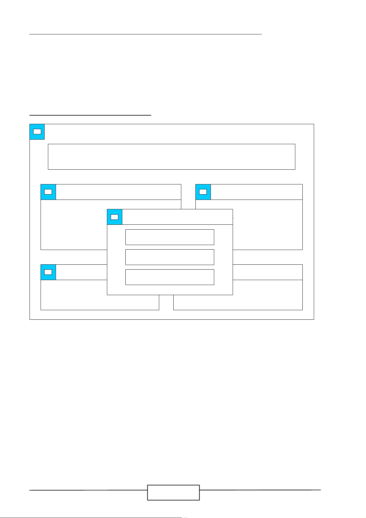
3.9 C
The “SECURITY” utility sets the password for
is shipped with the password disabled. When you select the “CHANGE SUPERVISOR
Password” on the main program, the screen display will appears as:
HANGE SUPERVISOR
SER PASSWORD
/ U
Supervisor
and
User
. The single board computer
Change Supervisor Password
American AMIBIOS Setup
Megatrends ©1994, American Megatrends, Inc.
Standard Advanced Chipset
Power Mgmt
Save Changes and Exit
DetectMaster DetectSlave
ColorSet
Do not save changes and Exit
Password Anti-Virus
Original Optimal Fail-Safe
Security :
l
Supervisor (Password)
l
User (Password)
l
Anti-Virus
Two Levels of Passwords :
If you use both, the Supervisor password must be set first. The system can be configured so that all
users must enter a password every time the system boots or when WINBIOS Setup is executed, using
either or both the Supervisor password or User password.
AMIBIOS Password Support :
Three icons appear in this part of the WINBIOS Setup screen –
Both the Supervisor and the User icons configure password support.
The Supervisor and User icons activate two different levels of
Page 54

AMI BIOS SETUP
password security. If WINBIOS Setup has an optional password feature. The system can be
configured so that all users must enter a password every time the system boots or when WINBIOS
Setup is executed.
Setting a Password :
Bookmark not defined. by choosing either
system is powered on) or
The password check option is enabled in Advanced Setup (see page Error!
Setup
Always
(the password prompt appears only when WINBIOS is run). The
(the password prompt appears every time the
password is encrypted and stored in NVRAM.
As shown on the above screen, you are prompted for a 1 - 6 character password. You can either type
the password on the keyboard or select each letter of the password, one at a time, using the mouse.
The password does not appear on the screen when typed. Make sure you write it down. If you forget it,
you must drain NVRAM and reconfigure.
If You Do Not Want to Use a Password :
Press <Enter> when the password prompt appears.
Changing a Password :
Select the
Supervisor
or
User
icon from the Security section of the
WINBIOS Setup main menu. Enter the p assword and press <Enter>. The screen does not display the
characters entered. After the new password is entered, retype the new password as prompted and
press <Enter>.
If the password confirmation is incorrect, an error message appears. If the new password is entered
without error, press <Esc>. The password is stored in NVRAM after WINBIOS completes. The next
time the system boots, a password prompt appears if the password function is present and enabled.
Remember the Password :
Keep a record of the new password when the password is changed.
If you forget the password, you must erase the system configuration information in NVRAM
(Non - Volatile Random Access Memory). See page Error! Bookmark not defined. for information
about erasing system configuration information. Note : If you forget your password, the only way to
solve this problem is to discharge the CMOS memory by turning power off and placing a shunt on the
S1 (open pad) for 5 seconds, then removing the shunt.
Under the Security window of the W INBIOS Setup screen, you can also select the Anti-Virus Icon.
Anti-Virus :
When this icon is selected from the Security section of the WINBIOS Setup main menu,
AMIBIOS issues a warning when any program (or virus) issues a Disk Format command or attempts
to write to the boot sector of the hard disk drive. The settings are Enabled or Disabled. If enabled,
the following appears when a write is attempted to the boot sector. You may have to type N several
times to prevent the boot sector write. Boot Sector W rite!!! Possible VIRUS: Continue (Y/N)? _
Page 55

AMI BIOS SETUP
The following appears after any attempt to format any cylinder, head, or sector of any hard disk drive
via the BIOS INT 13 Hard Disk Drive Service: Format!!! Possible VIRUS: Continue (Y/N)? _
3.10 U
In the Utility, the following icons appear in this section of the WINBIOS Setup main screen --
Color Set :
Language :
languages.
3.11 BIOS D
The icons of BIOS Defaults in this section permit you to select a group of settings for all WINBIOS
Setup options. Not only can you use these icons to quickly set system configuration parameters, you
can choose a group of settings that have a better chance of working when the system is having
configuration - related problems.
Original :
Setup when you first began this WINBIOS Setup session.
Optimal :
TILITY
Color Set sets the Setup screen colors.
If this feature is enabled, you can select WINBIOS Setup messages in different
EFAULTS
Choose the Original icon to return to the system configuration values present in WINBIOS
You can load the optimal default settings for the WINBIOS by selecting the Optimal icon.
The Optimal default settings are best-case values that should optimize system performance. If
NVRAM is corrupted, the Optimal settings are loaded automatically.
Fail-Safe BIOS Setup Settings :
selecting the Fail-Safe icon from the Default section of the WINBIOS Setup main menu.
The Fail-Safe settings provide far from optimal system performance, but are the most stable settings.
Use this option as a diagnostic aid if the system is behaving erratically.
You can load the Fail-Safe WINBIOS Setup option settings by
Page 56

TECHNICAL REFERENCE
APPENDIX A.
HOW TO USE WATCH-DOG TIMER
To use the watch-dog timer :
Step 1.
Step 2.
Enable and retrigger the Watch -Dog timer:
Disable:
i441
EX.1: For DOS
Execute the
according to the time-out you set.
For example, if you want to Set
JP16 : 1-2 ON
DEBUG.EXE
to enable watch-dog timer.
file under DOS, Then key-in
4 seconds
443H
i443
. The system will reboot automatically
for the time-out, you should set
JP9: 4L ON
and
C:\DOS> DEBUG
-i443
EX.2: For assemble Language
Enable :
:
:
IN AL, DX
:
:
Disable :
:
:
MOV DX, 443H
:
:
IN AL, 441H
Page 57

APPENDIX B.
TECHNICAL REFERENCE
I/O PORT ADDRESS MAP
Address Function
000 - 01F DMA Controller #1
020 - 03F Interrupt Controller #1
040 - 05F Timer Chip
043 Disable Watch-Dog Times Operation (Read)
060 - 06F Keyboard Controller
070 - 07F Read Time Clock/NMI Mask
080 - 09F DMA Page Register
0A0 - 0BF Interrupt Controller #2
0C0 - 0DF DMA Controller #2
0F0 - 0F1 Clear/Reset Math Coprocessor
1F0 - 1F7 Hard Disk Controller
200 - 210 Game Port
278 - 27F Parallel Port #2
2E8 - 2EF Serial Port #4 (COM 4)
2F8 - 2FF Serial Port #2 (COM 2)
300 - 31F prototype Card/Streaming Tape Adapter
360 - 36F PC Network
378 - 3FF Parallel Port #1
380 - 38F SDLC #2
3A0 - 3AF SDLC #1
3B0 - 3BF MDA Video Card (Including LPTO)
3C0 - 3CF EGA Card
3D0 - 3DF CGA Card
3E8 - 3EF Serial Port #3 (COM 3)
3F0 - 3F7 Floppy Disk Controller
3F8 - 3FF Serial Port #1 (COM 1)
443 Enable Watch -dog Timer Operation (read)
Page 58
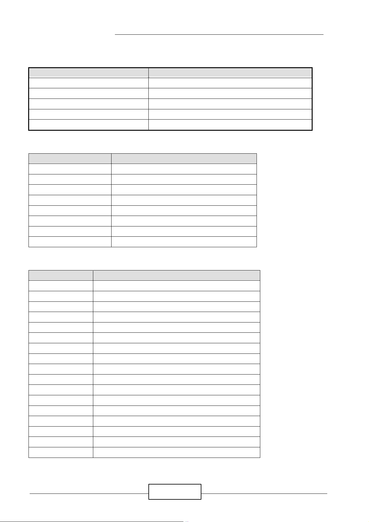
TECHNICAL REFERENCE
CHANNEL
Function
IRQ
Function
MEMORY ADDRESS MAP
DMA CHANNELS
INTERRUPT CONTROLLER
Page 59
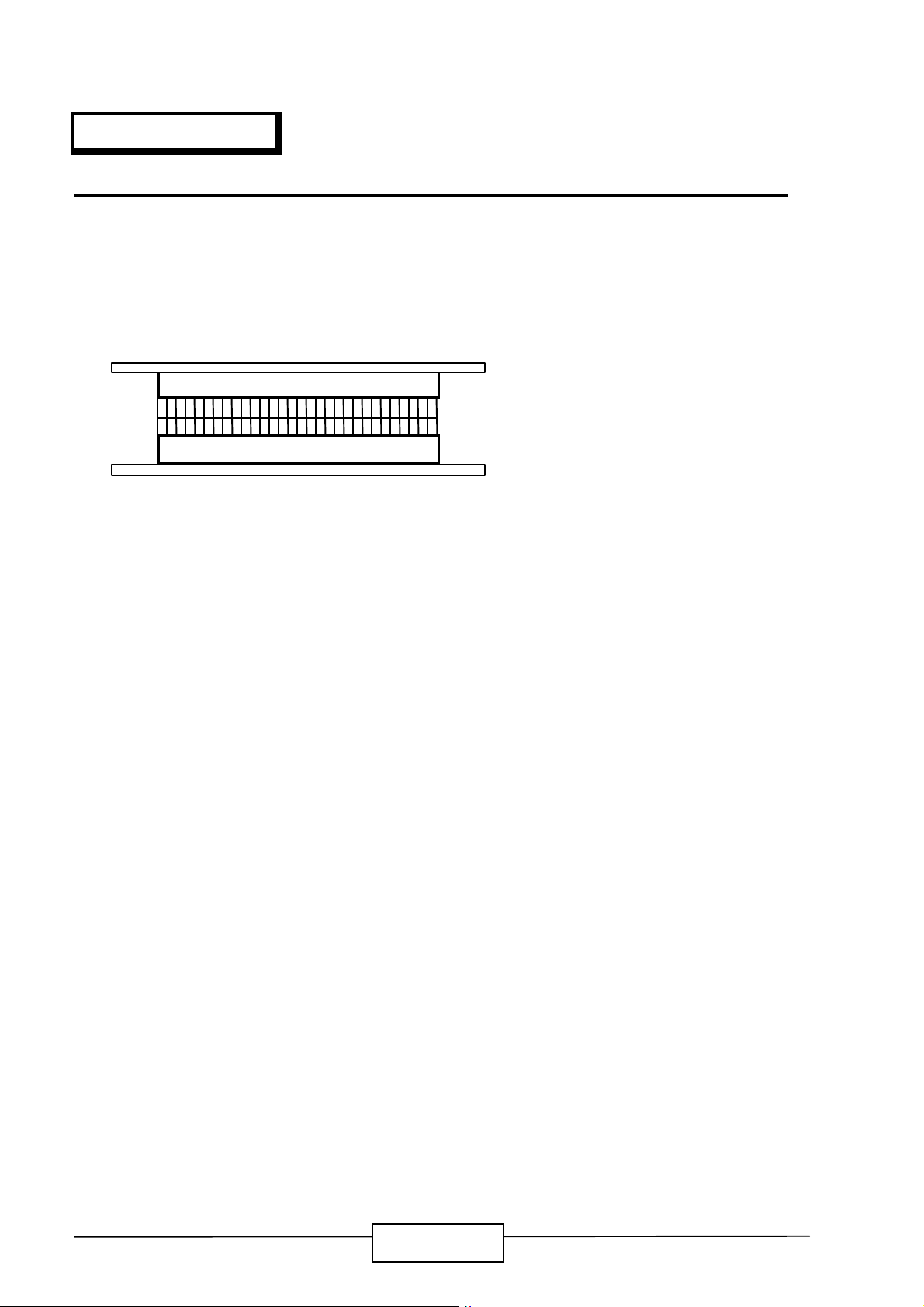
PCI Module
PCI Female Connector
AP-545V Single Board Computer
Dual-Side Male Connector
APPENDIX C.
PATENT PCI PIGGYBACK MODULE INSTALLATION
There are two steps to install out patent PCI pigyback module on AP-545V Single Board Computer.
Step 1.
Step 2.
Plug the Dual Side Male Connector into the patent PCI piggyback female connector.
Plug the PCI module‘s female connector into the AP-545V male connector.
Page 60

GLOSSARY
8-Bit Bus –
Data is transmitted to expansion slots and other components on the bus
only along 8 parallel data line.
10Base-T –
It is a 10Mbps IEEE 802.3/Ethernet standard that uses unshielded twisted pair cable
specification. 10Base-T supports network configuration using the CSMA/CD access method over a
twisted pair transmission system up to 100 meters in length without the use of repeater.
16-Bit Bus or ISA Bus –
Data is transmitted along either 8 or 16 data lines, depending
on what kind of adapter card is used in an expansion slot. ISA is the abbreviation of
Industry Standard Architecture.
100Base-TX –
It is a 100Mbps IEEE 802.3/Ethernet standard that uses UTP cable. Also called
Fast Ethernet, it uses RJ-45 connectors and EIA/TIA T568B pinning. Maximum cable length from
hub to node is 100 meters without a repeater.
Adapter –
It is also called an expansion board, expansion card, or adapter card. It is a
small circuit board that is installed in the expansion slots on the motherboard. You
can install a particular adapter that connects a new device such as internal modem,
sound card, and scanner.
AGP (Advanced Graphic Port ) –
is a new 32-bit interface, with external clock rate of 66MHz
that transmit a maximum of 528MB of data. It has a clock speed of 133MHz, which is four times the
speed of PCI interface.
bps –
Bits per second. Also often preceded by K (kilo/thousands),
and M (mega/million),
Mbps
– Mega bytes per second.
Kbps
– Kilo bytes per second,
BIOS (Basic Input /Output System) –
This is a chip on the motherboard that contains
the instructions for starting up, or booting, the computer, and more.
Bus –
Data that travels in a computer along the circuits on the motherboard are called
buses. Although three main buses (data bus, address bus, and control bus) manage
the computer’s operation, often these are collectively called the bus. The bus carries
instructions back and forth between the CPU and other devices in the system. ISA,
GLOSSARY
Page 61

EISA, VL-Bus, PCI and SCSI are examples of PC buses.
Bus Mastering –
A method of transferring data through a bus in which the device takes over the
bus and directly controls the transfer of data to the computer’s memory. Bus mastering is a method
of Direct Memory Access (
DMA
) transfer.
Cache –
Cache RAM is an extra holding area for program instructions that need to be
frequently used by the CPU or swapped in and out of RAM. Your CPU can usually
access those instructions from the cache more quickly than it could from a hard disk or
even RAM, so a cache helps the system work more efficiently. Most systems sold
today offer either 256K or 512K cache.
CPU (Central Processing Unit) –
executes all commands and controls the flow of
data, providing the “ brain ” that enables the PC to calculate and perform the
operations like sorting information more quickly than a human could. The CPU
makes perhaps the greatest contribution to a PC’s speed and power. Note: Any
additional information is subject to change without prior revision from the supplier.
Table 1 -- CPU Speeds
Processor type Speed ratings (MHz)
486DX2 66, 80
486DX4 75, 100, 120
Pentium 90, 100, 120, 133, 166, 200
Pentium MMX 166, 200, 233
Pentium Pro 166, 180, 200
Pentium II 233, 266, 300, 333
EIDE (Enhanced IDE) –
It is a hard drive controller that enables your system to be able
to handle fast hard disk drives at a speed of 10Mbps.
EISA or MCA Bus –
Data is transmitted along 32 data lines to adapter cards designed
specifically to work with the 32-bit buses. MCA expansion slots cannot accept 8-bit or
16-bit adapter cards. EISA stands for Extended Industry Standard Architecture, while
MCA stands for MicroChannel Architecture. MCA is architecture used in IBM
Microcomputer.
Page 62

GLOSSARY
Expansion slots –
Expansion slots are plug-in connectors that allow you to insert
additional circuit boards that attach to the rest of the PC through special circuitry called
bus
the
. By inserting the right circuit board -- usually called an
expansion card
– you can increase the resolution and the number of colors used by
adapter
or an
the display, or you can transform your PC into a machine for recording and playing
music.
Fast SCSI –
The common nomenclature associated with SCSI-2, the second generation of SCSI
offering mandatory parity checking improvements over SCSI-1.
IDE (Integrated Drive Electronics) –
It was developed from ST-506 type hard drive
interface, utilizes BIOS INT 13h hard drive secondary software and supports two hard
drives (Master and Slave). Do not need extra software to drive since it is directly
initiated in the BIOS. Data transfer rate is 4.1 Mbps. Take note that this interface
cannot support other drive like CD-ROM drive.
IEEE (Institute of Electrical and Electronic Engineers) –
It is an international professional
society that issues its own standard, and is a member of ANSI and ISO. Popular known standards
is:
IEEE802.3
– is a physical layer standard for 10Base-T,
100Base-T, Ethernet, and StarLAN.
IEEE802.5
IEEE802.11
– is a physical layer standard for Token Ring.
– is a physical layer standard for Wireless
LAN/WAN compatibility.
IEEE802.12
– is a physical layer standard for 100VG AnyLAN.
LAN (Local Area Network) –
A data communications network spanning a limited area. It
provides communications between three or more computers and peripherals, in most cases using a
high-speed media as it’s backbone.
Keyboard –
This is a component that comes in direct contact for you with your PC.
The mechanism of keyboard converts a key cap’s movement into a signal sent to the
computer. The most common key mechanism are “
contact
”. Capacitate keyboard has a spring that causes the plastic and the metal
capacitate
” and “
hard
plunger to move nearer to two pads that have large plates (plated in tin, nickel, and
copper). These pads are connected to the keyboard’s printed circuit board. Hard
Page 63

contact keyboard causes the key cap to collapse a foam rubber dome that presses
against a sheet of
GLOSSARY
plastic on the bottom of which is metallic area connected to the rest of the keyboard’s
circuit board.
LDCM (LANDesk Client Manager) –
With the help of LDCM, PCs that are either stand-alone or
on a network can not escape the control of a system administrator. Alerts will be sent to the user if
an abnormal condition is encountered in a PC. It allows the administrator to give each PC a thorough
check-up. Additionally, this feature is available to multiple OS’s on the market today. LDCM Key
Features include the following : ¬Health Monitoring
Accessibility
,¯
Extensive Instrumentation. This is a product from Intel.
, -
Real-Time Alerting
, ®
Remote
Mouse –
The keyboard is a barrier to learn how to use a computer. Xerox Corporation
first developed the concept of a pointing device, something a computer user could
move with his or her hand, causing a corresponding move on screen. Because of its
size and tail like cable, the device was named for the mouse. Apple Computer made
the mouse a standard feature of its Macintosh computers, and with the popularity of
Windows, a mouse is becoming standard equipment on all PCs, as well. The
Trackball
“
Digitizing tablets
“
” have survived more awkward methods of navigating with the keyboard.
” are popular with architects and engineers who must translate
precise movements of a pen into lines on the screen. “ Touch screens “, on which
you press either your finger and a special light pen to control the software, are too tiring
to use for any length of time.
MMXÔ –
CPU’s with MMXÔ technology are optimized to run multimedia application,
and therefore, offer faster multimedia playback than standard CPUs. However, when
manufacturers introduce any new hardware technology, the software makers need to
catch up. At this time of compilation, most applications can’t yet take advantage of
MMXÔ capabilities.
Parallel port –
Parallel ports (labeled
in printers. It is also often called a
printer port
with
. Although a serial port can also be used to send data from a PC to
LPT1, LPT2
, and so on) are usually for plugging
Centronics port
– has been almost synonymous
some models of printers, the parallel port is faster. A serial port sends data one bit at
a time over a single one-way wire; a parallel port can send several bits of data across
eight parallel wires simultaneously. Take note that a serial connection sends a single
Page 64

bit, a parallel port send an entire byte. A parallel connection has one drawback.
GLOSSARY
PCI Bus (Peripheral Component Interconnect) –
It is a connection slot in a motherboard
that supports 32-bit bus transfer rates. The now standard PCI Local Bus carries data along at least
32 lines, that is, at least 32 bits at a time. Local bus computer designs add special buses so the
CPU can communicate directly with key components like the monitor, resulting in much better
performance. You should look for PCI local bus capabilities in any system you buy, especially PCI
local bus video (which helps the monitor display more quickly).
POST (Power-On Self-Test) –
is the first thing your PC does when you turn it on, and
it’s your first warning of trouble with any of the components. When the POST detects
an error from the display, memory, keyboard, or other basic components, it produces
an error warning in the form of a message on your display and — in case your display is
part of the problem — in the form of a series of beeps.
RAM (Random Access Memory) –
consists of a bank of chips that act as “ working
memory ”, holding program instructions and data only while your computer’s on.
Unless the instructions and data are saved to a disk, RAM forgets them when you turn
your computer off. RAM is measured in megabytes (M). Most computers today
come with 32M of RAM, though some sell with only 16M installed. There are a few
different flavors and speeds of RAM, as well. One of the most prominent today is
Extended Data Output ( EDO ) RAM, but an even faster type of RAM that has just hit
the market is called
SyncDRAM
.
Serial port –
Serial ports are also sometimes called
ports, and are labeled
COM1, COM2
, and so on. It is simple in concept: one line to
COM
(short for COMmunications)
send data, another line to receive data, and a few other lines to regulate how data is
sent over the other two lines – from commonplace modems and printers to plotters and
burglar alarms. The most common use for serial port is with a
mouse
or
modem
The reason for this is that a serial port is not a very efficient way to transfer data, so
little data that speed is not crucial, and perfect for modems because. With current
technology, phone lines cannot transport more than one signal at a time anyway. The
serial port
is often referred to as an
RS-232 port
.
.
SCSI (Small Computer System Interface) –
An intelligent bus for transmitting data commands
between a variety of devices. There are many implementations of SCSI, including Fast SCSI, Wide
Page 65

SCSI, Fast Wide SCSI, Fast-20, and Fast-40.
Page 66

GLOSSARY
SCSI-2 –
The second generation of SCSI; includes many improvements to SCSI-1, including Fast
SCSI, Wide SCSI, and mandatory parity checking.
SCSI-3 –
The third generation of SCSI; introduces Fast-20 and Fast-40 as
improvements to the parallel bus. The standard also includes a number of specifications for
high-speed serial bus architectures such as SSA, Fiber Channel, and IEEE 1394. Also known as
Ultra SCSI.
Ultra SCSI –
Also known as SCSI-3, is a third generation SCSI standard that introduced parallel bus
speed improvements (FAST-20 and FAST-40), an the miniaturized 68-pin micro connector.
USB (Universal Serial Bus) –
USB consolidates serial, parallel, keyboard, mouse, and game
ports into one asynchronous and isochronous communications port with bandwidth for data transfer
speeds up to 12 Mbps without termination. By daisy-chaining USB hubs, up to 127 I/O devices can
be connected to one USB port on the PC. USB is completely plug-and play meaning peripherals can
be correctly detected and configured automatically as soon as they are connected.
UTP (Unshielded Twisted Pair) –
Twisted Pair
are two wires twisted together to reduce susceptibility to RF crosswalk.
Twisted pair cable with neither individual nor overall shielding.
VGA (Video Graphics Array) –
A video adapter that supports 640x480 pixels color resolution.
The Windows OS provides medium text & graphics standard.
VL-Bus –
It is also known as Local Bus; this is an I/O interface that is directly connected and
depended of the system CPU. The VL-Bus is an abbreviation of VESA Local Bus.
Page 67

Terms and Conditions
Date:1997.10.20
Warranty Policy
1. All products are warranted against defects in materials and workmanship on a period of two years
from the date of purchase by the customer.
2. The buyer will bear the return freight charges for goods that are returned for repair within the
warranty period whereas manufacturer will bear the other way after repair.
3. The buyer will pay for repair (for the replaced materials plus service time) and transportation charges
(both ways) for items after the expiration of the warranty period.
4. If the RMA Service Request Form does not meet the stated requirement as listed on “RMA Service
“ , RMA goods will be returned at the customer expense.
5. The following conditions are excluded from this warranty
A. Improper or inadequate maintenance by the customer.
B. Unauthorized modification or misuse.
C. Operation outside of the environmental specifications for the product.
:
RMA Service
1. Request a RMA# :
Complete and fax to Supplier the “RMA Request Form” to obtain a RMA number.
2. Shipping:
A. The customer is requested to fill up the problem code as listed . If none of the code is
selected, please write the symptom description on the remark.
B. Ship the defective units with freight prepaid.
C. Mark the RMA # clearly on the box.
D. Shipping damage as a result of inadequate packing is the customer‘s responsibility.
E. Use the original packing materials whenever possible .
3. All RMA# are valid for 30 days only:
When RMA goods are received after valid RMA# period , the goods will be rejected.
Page 68
RMA Service Request Form
Date:1997.10.20
When requesting RMA service, please fill out this “RMA Service Request Form”. This
form needs to be shipped with your returns. Service cannot begin until we have this
information.
Company: Person to contact:
Phone No. Purchased Date:
Fax No.: Applied Date:
Return Shipping Address
*For Supplier only
RMA No:
Account Sales:
Model No. Serial No. Problem Code Remark
*This form could be copied for more description
Problem Code
*
01:D.O.A.
02: Second Time R.M.A.
03: No Screen
04: CMOS Data Lost
05: FDC Fail
:
06: HDC Fail
07: Bad Slot
08: BIOS Problem
09: Keyboard Controller Fail
10: Cache RMA Problem
11: Memory Socket Bad
12: Hang Up Hardware
13: Hang Up Software
14: Other ( Pls. Specify )
Request Party Confirmed By Supplier
Page 69

Authorized Signatures Authorized Signatures
 Loading...