

Page 1

Embedded &
Industrial Computing
Hardware Platforms for Embedded and Industrial Computing
VES-500
V0.2
>>
User's Manual
Publication date:2014-08-22
Page 2
About
Overview
Icon Descriptions
The icons are used in the manual to serve as an indication
of interest topics or important messages. Below is a
description of these icons:
NOTE: This check mark indicates that
there is a note of interest and is something
that you should pay special attention to
while using the product.
About
WARNING: This exclamation point
indicates that there is a caution or
warning and it is something that could
damage your property or product.
Online Resources
The listed websites are links to the on-line product
information and technical support.
Resource Website
Lanner http://www.lannerinc.com
Product Resources http://assist.lannerinc.com
RMA http://eRMA.lannerinc.com
Copyright and Trademarks
This document is copyrighted, © 2014 All rights are
reserved. The original manufacturer reserves the right to
make improvements to the products described in this
manual at any time without notice.
No part of this manual may be reproduced, copied,
translated or transmitted in any form or by any means
without the prior written permission of the original
manufacturer. Information provided in this manual is
intended to be accurate and reliable. However, the original
manufacturer assumes no responsibility for its use, nor for
any infringements upon the rights of third parties that
may result from such use.
Embedded and Industrial Computing
2
Page 3

TTaTTable of Contentsbeable of Contents
Chapter 1: Introduction 4
System Specication . . . . . . . . . . . . . . . . . . . . . . . . . . . . . . . . . . . . . . . . . . . 4
Package Contents . . . . . . . . . . . . . . . . . . . . . . . . . . . . . . . . . . . . . . . . . . . . . 5
Chapter 2: System Components 6
System Drawing . . . . . . . . . . . . . . . . . . . . . . . . . . . . . . . . . . . . . . . . . . . . . . 6
Block Diagram: The MainBoard . . . . . . . . . . . . . . . . . . . . . . . . . . . . . . . . . . . . . 7
Front Features. . . . . . . . . . . . . . . . . . . . . . . . . . . . . . . . . . . . . . . . . . . . . . . . 8
Rear Features . . . . . . . . . . . . . . . . . . . . . . . . . . . . . . . . . . . . . . . . . . . . . . . . 9
Chapter 3: Motherboard Information 10
Motherboard Layout- Top View. . . . . . . . . . . . . . . . . . . . . . . . . . . . . . . . . . . . .10
Power Ignition Board Layout- Top View. . . . . . . . . . . . . . . . . . . . . . . . . . . . . . . .11
Power Ignition Board Layout-Bottom View . . . . . . . . . . . . . . . . . . . . . . . . . . . . .11
Connectors and Jumpers List. . . . . . . . . . . . . . . . . . . . . . . . . . . . . . . . . . . . . .12
Jumper Settings . . . . . . . . . . . . . . . . . . . . . . . . . . . . . . . . . . . . . . . . . . . . . .13
Appendix A: Programming the MCU 18
Appendix B: Terms and Conditions 20
Warranty Policy . . . . . . . . . . . . . . . . . . . . . . . . . . . . . . . . . . . . . . . . . . . .20
RMA Service . . . . . . . . . . . . . . . . . . . . . . . . . . . . . . . . . . . . . . . . . . . . . .20
3
Page 4
Chapter 1
Chapter 1:
Introduction
Thank you for choosing the VES-500. The VES-500 is
Lanner’s flagship Single Board Computer. It features
Freescale IMX6 series processors.
This computer-on-module consists of a motherboard
populated with the Freescale® iMX6™ series processor,
providing a rich I/O capabilities and flexibility via highbandwidth interfaces such as Mini-PCI Express sockets,
Serial ATA, and Hi-Speed USB 2.0 connectivity.
It also contains advanced I/O connectors as the following
listed:
-built-in GPS (provided by Neo-6Q) and G sensor
-Internl MIPI (Mobile Industry Processor Interface)
connector
-Wide range of DC power input from 9V to 30V, suitable
for vehicular 12V or 24V battery with Ignition control (with
VEK-IGN01 ignition board).
-CAN bus Connector via DB-9 female connector
-Dual Mini-PCI Express Sockets (one comes with a SIM card
reader for 3G Internet service)
-External SIM card reader
-External SD card reader
-Line-out/microphone jack as well as HDMI connector
The platform is supported by a Linux BSP as well as
multiple third party operating systems and reference
implementations that allow fast time to market and rapid
prototyping. We include development instructions in
the BSP folder in the Driver and User Manual CD. More
information can be found at http://www.freescale.com/
webapp/sps/site/prod_summary.jsp?code=i.MX6Q. Note
that some documentation and software may require you
to register first.
Introduction
System Specification
System
CPU
System Memory Onboard DDR3 SDRAM
Storage Onboard 4GB eMMC ash and SD card socket
Expansion
DC-in and Power Ignition
Connector
MCU Programming and
Digital I/O
USB
Mini-PCIe Expansion
CAN (Controller Area
Network) BUS
MIPI
SATA 1 SATA drive and power connector
GPS
G Sensor G Sensor
Chipset Intel Integrated Graphics
LVDS 1 x 2x15-pin 24-bit LVDS output
HDMI 1 x HDMI connector
Connectors Line-out and Mic-in audio jack
LAN Chip
Ethernet Interface RJ45 with LED, 10/100/1000Mbps
Internal Serial Port
Power requirement +12V DC-in
Optional power require-
ment (with PoE board
VEK-PDM01)
Optional PoE (PD)
Operating Temperature -20 ~TBD°C (depending on chassis design)
Storage Temperature -20 ~ 70°C (-4 ~ 158°F)
Operating Humidity 5% ~ 95% Relative Humidity, Non-condensing
Size (L x W) 230 mm x 145mm
Weight 0.2 kg (0.44 lbs)
Freescale iMX6 series processors: quad Core (VES500A)/dual core (VES-500B)
Power Ignition board: VEK-IGN01
Power over Ethernet: VEK-PDM01
I/O
3-pin power-in connector with ignition control provided by ignition board VEK-IGN01
D-sub 9 Male Connector for MCU programming and
digital I/O function provided by VEK-IGN01
2x USB 2.0 type A (host and Usb On-The-Go, 1x5 pin
header
2 Mini-PCIe connector supporting only USB interface;
one comes with a SIM card reader
CAN bus connector via DB-9 female
Internal MIPI (Mobile Industry Processor Interface)
connector (reserved)
1x GPS chip (Neo-6Q) with SMA connector for
antenna
Display
Audio
Ethernet
1 x Atheros AR8031PCI express
1x Ethernet controller
Console
One internal 3-pin pin header for serial communication
Mechanical & Environmental
9~30Vdc in for wide range power input with MCU
controlled ignition function
Powered device (PD for PoE) with default power
request 25W (802.3at)
Embedded and Industrial Computing
4
Page 5

Chapter 1
Package Contents
Your package contains the following items:
VES-500 System Board •
DC+12V 60W Power Adapter •
Console Cable •
Power Device Module: VEK-PDM01 •
Power Ignition Module: VEK-IGN01 •
Introduction
Embedded and Industrial Computing
5
Page 6
Chapter 2
Chapter 2:
System Components
System Drawing
Mechanical dimensions of the VES-500
Unit: mm
System Components
230
145
Embedded and Industrial Computing
6
Page 7
Chapter 2
1GB
DDR3
FreeScale
i.MX6
Processor
DDR3
RGMII
PF0100
PMIC
JTAG
USB Hub
USB
SD Card
Connector
HDMI
Connector
PMIC
4MB
eMMC
Flash
Ethernet
Atheros
AR8031
USB Host (Type
A)
USB
12V
DC
12V
PWM
Power Ignition
VEK-
PDM01
VEK-
IGN01
CANbus
CANbus
Connector
SATA
Connector
SATA
LVDS
LVDS Connector
G Sensor
(MMA8451)
I2C
GPS
Mini-PCIe
Connector II
PoE
PCIe
USB 2.0
Mini-PCIe
Connector I
(with SIM Card
Reader)
USB 2.0
UART 1
Console
USB
OTG
8$57
USB Connector
(1x5 Pin
Header)
Block Diagram: The MainBoard
The block diagram depicts the relationships among the
interfaces and modules on the motherboard.
System Components
Embedded and Industrial Computing
7
Page 8

Chapter 2
Front Features
System Components
F1
F1 Power (Green) /HDD (Yellow) LEDs
LED Behavior Interpretation
Power (Green) On/Flashing The system is powered on.
HDD (Yellow) Flashing It indicates data access activity
F2 Two USB 2.0 Ports (left: USB Host, right: USB On-The-Go)
The left one is Host USB; the left one can act as a host as well as a device with jumper settings. Refer to
pin HOSTUSB1 and OTGUSB1 in Chapter 3 Motherboard Information for pin definitions.
F2
O The system is powered o..
O There are no data access activities or no
F3
F4 F5
hard disk present
F6
F3 SD Card Connector
Refer to pin SDC1 for pin definitions in Chapter 3 Motherboard Information.
F4 F5 Microphone/Line-out Connector
Refer to pin MIC1 and Front1 for pin definitions in Chapter 3 Motherboard Information.
F6 Reset Button
It is a reset button to turn on or off the power. The reset button can act as a hardware to reset the entire
system or software reset to reset the designated software to its default. It can also be used as power
on/off switch with jumper settings. Refer to Pin RST1 and SW3 for more information on jumper settings
in Chapter 3 Motherboard Information .
Embedded and Industrial Computing
8
Page 9

Chapter 2
Rear Features
System Components
R2
R1
R1 SIM Card Reader
Refer to pin SIM1 for pin definition in Chapter 3 Motherboard Information.
R2 CAN bus Connector
Refer to Pin CAN1 for pin definition in Chapter 3 Motherboard Information.
R3 HDMI Connector
Refer to pin HDMI1 for pin definition in Chapter 3 Motherboard Information.
R4 One10/100/1000Mbps LAN port
The connector is provided by Atheros AR8031PCI express controller and can be a powered device for PoE
function (with VEK-PDM01 PoE board). Refer to Pin LAN1 for pin definition in Chapter 3 Motherboard
Information.
R3
R4
R5
LED Behavior Interpretation
LINK/ACT (Left, Yellow) On/Flashing The port is linking.
O The port is not linking.
SPEED (Right, Green/Amber) Amber The connection speed is 1000Mbps.
Green The connection speed is 100Mbps.
O The connection speed is 10Mbps.
R5 Power Adapter socket with Lock
DC-in 12V jack. Only use the power adapter supplied with the VES-500 System.
Embedded and Industrial Computing
9
Page 10

Chapter 3
Chapter 3:
Motherboard Information
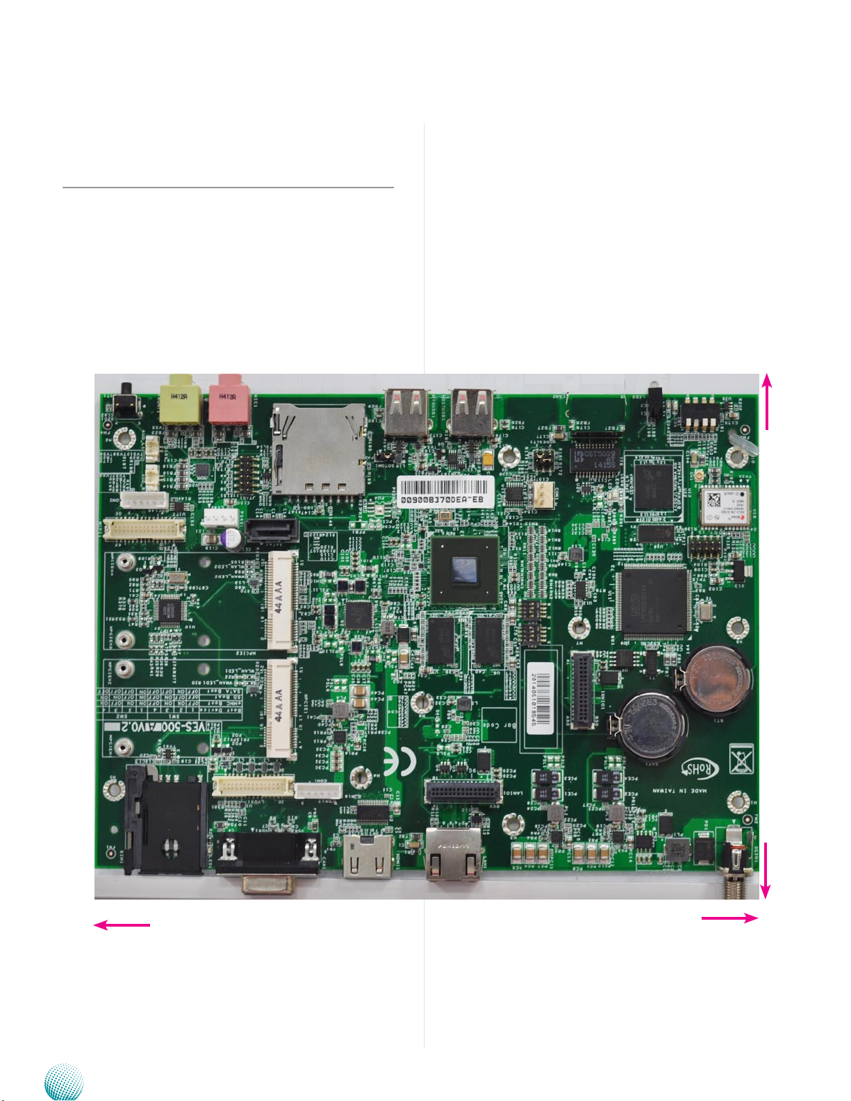
Motherboard Layout- Top View
The motherboard layout shows the connectors and
jumpers on the board. Refer to the following picture and
table 3.1 as a reference of the pin assignments and the
internal connectors.
Motherboard Information
SW1
SW2
DCIN1
IGNIO1
LANIO1
LAN1
HDMI1
CON1
CAN1
LVDS1
SIM1
MPCIE1
MPCIE2
COM1
SW3
Embedded and Industrial Computing
MODESLT1
HOSTUSB1
OTGUSBB1
SOTGM1
SDC1
SATA1
MIC1
JTAG1
PS4S1
MIPI1
CON2
AUD_R1
AUD_L1
RST1
FRONT1
VES-500
10
Page 11

Chapter 3
Power Ignition Board Layout- Top View
The motherboard layout shows the connectors and
jumpers on the board. Refer to the following picture and
table 3.2 as a reference of the pin assignments and the
internal connectors.
SW1
Motherboard Information
PRJK1
Power Ignition Board Layout-Bottom View
The motherboard layout shows the connectors and
jumpers on the board. Refer to the following picture and
table 3.2 as a reference of the pin assignments and the
internal connectors.
DGIO1
Embedded and Industrial Computing
IGNI01
VEK-IGN01
11
Page 12

Chapter 3
Motherboard Information
Connectors and Jumpers List
The tables below list the function of each of the board
jumpers and connectors by labels shown in the above
section. The next section in this chapter gives pin
definitions and instructions on setting jumpers.
Table 3.1 Connector List for VES-500 Board
Labels Function Pin Denition Reference Page
CAN1 CANbus Connector P14
COM1 Serial COM Port P13
CON1 LVDS Power Connector P13
CON2 USB Connector P13
DCIN1 DC-in Jack P14
FRONT1 Front Headphone Connector P15
HDMI1 High-Denition Multimedia Interface P14
HOSTUSB1 Host USB Connector P15
IGNIO1 Ignition Board Connector P15
JTAG1 JTAG Connector P14
LAN1 Ethernet LAN Connector P13
LANIO1 PoE (PD) module P15
LVDS1 Low-voltage Dierential Signaling Connector P14
MIC1 Microphone Connector P15
MIPI1 Mobile Industry Processor Interface P14
MODESLT1 Boot Mode Selection P13
MPCIE1 Mini-PCIe Connector P16
MPCIE2 Mini-PCIe Connector P16
OTGUSB1 On-the-Go USB Connector P15
PS4S1 SATA Power Connector P13
RST1 Reset Button P13
SATA1 SATA Drive Connector P13
SDC1 SD Card Reader P14
SIM1 SIM Card Reader P15
SOTGM1 OTGUSB1 master/slave Selection P15
SW1/SW2 System Boot Device Selection P13
SW3 RST1 Function Selection P13
Table 3.2 Connector List for VEK-IGN01 Board
Labels Function Pin Denition Reference Page
DGIO1 External Connector for MCU Programming and
Digital I/O
IGNIO1 Connector to the Main Board P17
PRJK1 DC-in Power Connector P17
SW1 MCU (Microcontroller) Function Selection P17
Embedded and Industrial Computing
P17
12
Page 13

Chapter 3
Motherboard Information
Jumper Settings
VES-500 Board:
CON1: For LVDS power
Pin No. Signal
1 5V
1 2 3 4 5 6
Internal USB 2.0 Connector (CON2)
1 2 3 4 5 6
4-pin Reset or Power-on Push Button (RST1): This
button can be pushed to power up or reset the system
depending on the jumper setting (J2).
3
1
RST1 Function Selection (SW3): It is used for
selecting the RST1 push button’s function.
2 CAP_TCH_INT0
3 GND
4 LVDS0_TOUCH_SDA
5 LVDS0_TOUCH_SCL
6 GND
Pin No. Signal
1 5V
2 CAP_TCH_INT0
3 GND
4 USB_D+
5 USB_D6 GND
Pin No. Signal
4
2
1 GND
2 RST
3 GND
4 N/A
System Boot Device Selection (SW1, SW2): It selects
between the onboard eMMC or the SD card to be the
boot device.
Boot Device Selection
SD4== eMMC memory
SD2== SD card
SW2 SW1
1 2 3 4 1 2 3 4
1 2 3 4 5 6 7 8
11=SD4
boot
10=SD2
boot
0 X X X 0100=SATA Boot
0 0 0 0 1100=Download Mode
Where x: don’t care
1X=4-bit X110 = MMC/eMMC
01=8-bit
0X=1-bit X010 = SD/eSD
1X=4-bit
Boot
Boot
SATA Connector (SATA1): It is for connecting a 2.5’’
SATA harddisk to be served as your system’s storage. It
supports rates up to 3.0 Gb/s (300 MB/s) with Integrated
AHCI controller
Pin No. Signal
1 GND
2 TX+
7 6 5 4 3 2 1
3 TX4 GND
5 RX6 RX+
7 GND
4 3 2 1
5 6 7 8
Selector. Functkon
1 On Power On/Off
2 On H/W Reset
3 On Software Reset
4 ON MCU Reset
Serial Port(COM1)
3
2
1
Pin No. RS-232 Signal
1
2
3
RXD
GND
TXD
MODESLT1: Boot mode Selection
2
1
Pin Setting. Function
3-5, 4-6 Boot From fuses (for freescale debug)
3-5, 2-4 Serial Downloader (for memory test parameter collection)
1-3, 4-6 Boot from board settings
1-3, 2-4 Reserved
Embedded and Industrial Computing
6
5
4-pin SATA Power Connector (PS4S1): It is used for
connectig the SATA power cord.
4 3 2 1
PIN NO. 1 2 3 4
Signal +12V GND GND +5V
LAN1: PoE Ethernet Port
Pin No. Signal Pin No. Signal
1 POE_MDI0P 7 POE_MDI3P
2 POE_MDI0N 8 POE_MDI3N
3 POE_MDI1P 9 P1_LED_ACT
4 POE_MDI2P 10 LED_LINK_SPD_N
5 POE_MDI2N 11 LED_LINK10_100
6 POE_MDI1N 12 P1_LED_LINK1000
13
Page 14

Chapter 3
Motherboard Information
Left and Right Speaker Connecotr (AUD_R1&L1)
2
1
AUD_R1/AUD-L1
AUD_L1 AUD_R1
PIN NO. Signal PIN NO. Signal
1 SPKLN 1 SPKRN
2 SPKLP 2 SPKRP
Jtag Connector (JTAG1): The 3-pin connector is for
connecting the system fan.
12
10
Pin No. Pin Name Pin NO. Pin Name
1 JTAG_VREF 2 VCC3
3 nTRST 4 GND
5 TDI 6 PIN13_PD
7 TMS 8 nSRST
9 TCK 10 DE
11 RTCK 12 DACK
11
8
6
4
2
9
7
5
3
1
DC Power-in Connector (DCIN1)
Pin No. Pin Name
1 12V
2 GND
3 GND
High-Definition Multimedia Interface (HDMI1): HighDefinition Multimedia Interface
Pin NO. Function Pin NO. Function
1 HDMI_DATP2_P 10 HDMI_CLK_P
2 GND 11 GND
3 HDMI_DATP2_N 12 HDMI_CLK_N
4 HDMI_DATP1_P 13 N/A
5 GND 14 N/A
6 HDMI_DATP1_N 15 HDMI_DDC_CLK
7 HDMI_DATP0_P 16 HDMI_DDC_DAT
8 GND 17 GND
9 HDMI_DATP0_N 18 PHDMI
Mobile Industry Processor Interface (MIPI1)
Pin NO. Function Pin NO. Function
1 GND 2 GND
3 GND 4 CSI_SDA
5 1V8 6 CSI_SCL
7 COMS2_1V8 8 CSI_RST_B
9 1V8 10 GND
11 GND 12 CSI_PWN
13 COMS2_2V8 14 GND
15 GND 16 CSI_D1P
17 GND 18 CSI_D1M
19 CSI_MCLK 20 GND
21 GND 22 CSI_CLK0P
23 GND 24 CSI_CLK0M
25 CAM2_1V5 26 GND
27 GND 28 CSI_D0P
29 GND 30 CSI_D0M
1 29
2 30
19 HDMI_HPD
LVDS Connector (LVDS1):
30 2
29 1
Pin NO. Function Pin NO. Function
1 VCC3 2 VCC3
3 GND 4 GND
5 N/A 6 LCD_VDD
7 LVDS0_TX0_NEG 8 BL_EN
9 LVDS0_TX0_POS 10 DISP0_CONTRAST
11 GND 12 GND
13 LVDS0_TX1_NEG 14 LVDS0_EDID_SCL
15 LVDS0_TX1_POS 16 LVDS0_EDID_SDA
17 GND 18 GND
19 LVDS0_TX2_NEG 20 LVDS0_TOUCH_SCL
21 LVDS0_TX2_POS 22 LVDS0_TOUCH_SDA
23 GND 24 GND
25 LVDS0_CLK_NEG 26 CAP_TCH_INT0
27 LVDS0_CLK_POS 28 LCD_VDD
29 GND 30 GND
Embedded and Industrial Computing
SDC1: SD Card Reader
Pin NO. Signal Pin NO. Signal
1 SD2_DATA3 PAD1 SD2_CD
2 SD2_CMD PAD2 SD2_WP
3 GND PAD3 GND
4 VCC3
5 SD2_CLK
6 GND
7 SD2_DATA0
8 SD2_DATA1
9 SD2_DATA2
CAN bus Connector (CAN1)
Pin NO. Signal
5 4 3 2 1
9 8 7 6
1 NC
2 GND
3 CANH
4 NC
5 CANL
6 NC
7 NC
8 NC
9 NC
14
Page 15

Chapter 3
Motherboard Information
Microphone Connector (MIC1):
Pin No. Pin Name
1 GND
2 MIC_RAW
3 GND
4 MICROPHONE_DET
5 MICBIAS2_RAW
Ignition Board Connector (IGNIO1): It is for connecting
the power ignition boardVEK-IGN01.
Pin NO.. Function Pin NO. Function
A1 GND B1 P12V_SB1
A2 GND B2 P12V_SB1
A3 GND B3 P12V_SB1
A4 GND B4 P12V_SB1
A5 GND B5 P12V_SB1
A6 GND B6 P12V_SB1
A7 GND B7 P12V_SB1
A8 GND B8 P12V_SB1
A9 GND B9 N/A
A10 GND B10 P5VA
A11 GND B11 P5VA
A12 N/A B12 N/A
A13 UART2_TX B13 PWR_EN
A14 UART2_RX B14 SYS_PG
A15 N/A B15 N/A
PoE power-device (PD) module Connector (LANIO1): It
is for connecting the POE powered device (PD) board VEK
PDM01 or the VEKTFM01.
+12V DC-in Jack (DCIN1)
Pin No. Pin Name
1 +12V DC-IN
2 GND
3 GND
HOST USB Connector (HOSTUSB1)
Pin No. Signal
1 H1_VUSB
1 2 3 4
2 USB_HOST_DN
3 USB_HOST_DP
4 Ground
On-The-Go USB Connector (OTGUSB1): The USB
OTG can perform both master and slave roles in USB
communications. Besides the 2 external USB type A
connectors, an internal pin header is provided for an
additional USB port.
Pin No. Signal
1 OTG_VUSB
2 USB_OTG_DN
1 2 3 4
3 USB_OTG_DP
4 Ground
OTGUSB1 Mode Selection (SOTGM1): It selects the
OTGUSB1 to be either the host (master) or the device
(slave).
Pin NO.. Function Pin NO. Function
A1 GND B1 GND
A2 POE_MDI3N B2 LAN1_MDI3N
A3 POE_MDI3P B3 LAN1_MDI3P
A4 POE_MDI2N B4 LAN1_MDI2N
A5 POE_MDI2P B5 LAN1_MDI2P
A6 POE_MDI1N B6 LAN1_MDI1N
A7 POE_MDI1P B7 LAN1_MDI1P
A8 POE_MDI0N B8 LAN1_MDI0N
A9 POE_MDI0P B9 LAN1_MDI0P
A10 GND B10 GND
A11 N/A B11 PWR_EN
A12 GND B12 P12V_SB1
A13 GND B13 P12V_SB1
A14 GND B14 P12V_SB1
A15 GND B15 P12V_SB1
SIM Card Reader (SIM1)
Front Speaker Connector (FRONT1): Theses pin headers
provide function for speaker/headphone connection.
Pin No. Signal
1 GND
2 HP_L
3 GND
4 HEADPHONE_DET
5 HP_R
Embedded and Industrial Computing
3 2 1
C5
C7
Pin NO. Signal Pin NO. Signal
C1 UIM_PWR C5 GND
C2 UIM_RST# C6 UIM_VPP
C3 UIM_CLK C7 UIM_DATA
Pin No. Function
2-3 Host Mode
1-2 Device Mode
C1
C3
15
Page 16

Chapter 3
Mni-PCIe Connector (MPCIE1): This socket comes with a
SIM card. Note it only supports USB signal/interface MiniPCIe card.
Pin NO.. Signal Pin NO. Signal
1 N/A 2 VCC3.3
3 N/A 4 GND
5 N/A 6 N/A
7 N/A 8 USIM_PWR
9 GND 10 UIM_DATA
11 N/A 12 UIM_CLK
13 N/A 14 UIM_RESET
15 GND 16 UIM_VPP
17 RSV 18 GND
19 RSV 20 N/A
21 GND 22 N/A
23 N/A 24 VCC3.3
25 N/A 26 GND
27 GND 28 N/A
29 GND 30 N/A
31 N/A 32 N/A
33 P N/A 34 GND
35 GND 36 USB_N1
37 GND 38 USB_P1
39 VCC3.3 40 GND
41 VCC3.3 42 N/A
43 GND 44 N/A
45 RSV 46 N/A
47 RSV 48 N/A
49 RSV 50 GND
51 RSV 52 VCC3.3
Motherboard Information
Mni-PCIe Connector (MPCIE2): It supports USB and PCIe
signal/interface Mini-PCIe card.
Pin NO.. Signal Pin NO. Signal
Pin Signal Pin Signal
1 WAKE# 2 VCC3.3
3 N/A 4 GND
5 N/A 6 N/A
7 CLKREQ# 8 N/A
9 GND 10 N/A
11 PCIE_CLK _N 12 N/A
13 PCIE_CLK _P 14 N/A
15 GND 16 N/A
17 RSV 18 GND
19 RSV 20 N/A
21 GND 22 PLTRST
23 PCIE_RX_N 24 VCC3.3
25 PCIE_RX_P 26 GND
27 GND 28 VCC1.5
29 GND 30 SMBCLK
31 PCIE_TX_N 32 SMBDATA
33 PCIE_TX_P 34 GND
35 GND 36 USB_N2
37 GND 38 USB_P2
39 VCC3.3 40 GND
41 VCC3.3 42 N/A
43 GND 44 N/A
45 RSV 46 N/A
47 RSV 48 VCC1.5
49 RSV 50 GND
51 RSV 52 VCC3.3
Embedded and Industrial Computing
16
Page 17

Chapter 3
VEK-IGN01
Power-in with Ignition Control (PRJK1): A power
connector with power -ignition Control.
Motherboard Information
1 2 3
Pin No. Pin Name
1 Ignition
2 GND
3 DC_VIN
An external connector for MCU programming and
Digital I/O (DGIO1)
1 2 3 4 5
6 7 8 9
Pin No. Pin Name Pin No. Pin Name
1 IGN_OUT0
(digital_out bit 0)
2 EXT_TXD 7 IGN_DI1
3 EXT_RXD 8 IGN_DI2
4 IGN_OUT1
(digital_out bit 1)
5 GND
6 IGN_DI0
(digital_in bit 0)
(digital_in bit 1)
(digital_in bit 2)
9 IGN_DI3
(digital_in bit 3)
Connector to the main board (IGNIO1)
Pin NO.. Function Pin NO. Function
A1 GND B1 P12V_SB1
A2 GND B2 P12V_SB1
A3 GND B3 P12V_SB1
A4 GND B4 P12V_SB1
A5 GND B5 P12V_SB1
A6 GND B6 P12V_SB1
A7 GND B7 P12V_SB1
A8 GND B8 P12V_SB1
A9 GND B9 N/A
A10 GND B10 P5VA
A11 GND B11 P5VA
A12 N/A B12 N/A
A13 UART2_TX B13 PWR_EN
A14 UART2_RX B14 SYS_PG
A15 N/A B15 N/A
MCU (Microcontroller) Function Selection (SW1):
Function
Selector No.
1-On, 2-On On (default) Off (default)
3-On, 4-On Off (program download) On (program download)
5-On Off Off
6-On Off On
Embedded and Industrial Computing
Normal Program MCU
17
Page 18

Appendix A
Appendix A:
Programming the MCU
The MCU programs is by way of the follwing method:
Host communication interface: RS-232•
Support buad rate: 57600/ 8N1•
Communication protocol: ANSI terminal.•
Digital Input/Output Control
The above command sets POWERON_DELAY =10
The MCU commands:
MCU
Command
PowerOn
Delay
(Sec)
PowerO
Delay
(Sec)
Current
Power
State
Wirte/Read
(SET/GET)
SET POWERON_
GET POWERON_
SET SHUTDOWN_
GET SHUTDOWN_
GET POWER_
VariableName value De-
DELAY
DELAY
DELAY
DELAY
STATE
fault
4(default) 4S
4(default) 4S
Example
1. Set the delay time for power-on delay:
>SET POWERON_DELAY 4 (Set powe-on delay to 4
seconds)
>OK (System response)
>GET POWERON_DRLAY (Get the power-on delay time)
in seconds
>POWERON_DELAY=4 (System response)
The above command sets SHUTDOWN_DELAY=10
2. Read the current power state
GET POWER_STATE (Get power state command)
POWER_STATE=STARTUP (System response)
The above command reads the current power state.
3. Read/write digital output state
Embedded and Industrial Computing
>SET DIGITAL_OUT 3 (set digital_out bit 0=1 and digital_
out bit 1=1)
>OK
18
Page 19

Appendix A
>Get DIGITAL_OUT
>DIGITAL_OUT=3
4. Read Digital_In state
GET DIGITAL_IN (Get digital_input state)
DIGITAL_IN= 3 (System response)
Digital Input/Output Control
Embedded and Industrial Computing
19
Page 20

Appendix B
Terms and Conditions
Appendix B:
Terms and Conditions
Warranty Policy
All products are under warranty against defects in 1.
materials and workmanship for a period of one year
from the date of purchase.
The buyer will bear the return freight charges for 2.
goods returned for repair within the warranty period;
whereas the manufacturer will bear the after service
freight charges for goods returned to the user.
The buyer will pay for repair (for replaced components 3.
plus service time) and transportation charges (both
ways) for items after the expiration of the warranty
period.
If the RMA Service Request Form does not meet the 4.
stated requirement as listed on “RMA Service,” RMA
goods will be returned at customer’s expense.
The following conditions are excluded from this 5.
warranty:
RMA Service
Requesting a RMA#
To obtain a RMA number, simply fill out and fax the 6.
“RMA Request Form” to your supplier.
The customer is required to fill out the problem code 7.
as listed. If your problem is not among the codes listed,
please write the symptom description in the remarks
box.
Ship the defective unit(s) on freight prepaid terms. 8.
Use the original packing materials when possible.
Mark the RMA# clearly on the box. 9.
Note: Customer is responsible for shipping
damage(s) resulting from inadequate/loose
packing of the defective unit(s). All RMA# are valid
for 30 days only; RMA goods received after the
effective RMA# period will be rejected.
Improper or inadequate maintenance by the •
customer
Unauthorized modification, misuse, or reversed •
engineering of the product.
Operation outside of the environmental specifications •
for the product.
Embedded and Industrial Computing
20
Page 21

Appendix B
RMA Service Request Form
When requesting RMA service, please fill out the following form. Without
this form enclosed, your RMA cannot be processed.
RMA No:
Reasons to Return: Ŀ Repair(Please include failure details)
Ŀ Testing Purpose
Company: Contact Person:
Phone No. Purchased Date:
Fax No.: Applied Date:
Return Shipping Address:
Shipping by: Ŀ Air Freight Ŀ Sea Ŀ Express ___
Ŀ Others:________________
Item Model Name Serial Number Configuration
Item Problem Code Failure Status
*Problem Code:
01:D.O.A.
02: Second Time
R.M.A.
03: CMOS Data Lost
04: FDC Fail
05: HDC Fail
06: Bad Slot
07: BIOS Problem
08: Keyboard Controller Fail
09: Cache RMA Problem
10: Memory Socket Bad
11: Hang Up Software
12: Out Look Damage
13: SCSI
14: LPT Port
15: PS2
16: LAN
17: COM Port
18: Watchdog Timer
19: DIO
20: Buzzer
21: Shut Down
22: Panel Fail
23: CRT Fail
24: Others (Pls specify)
Request Party
Confirmed By Supplier
Authorized Signature / Date Authorized Signature / Date
Terms and Conditions
Embedded and Industrial Computing
21
 Loading...