

Page 1

Embedded &
Industrial Computing
Hardware Platforms for Embedded and Industrial Computing
VES-310
V1.1
>>
User's Manual
Publication date:2014-03-05
Page 2
About
About
Overview
Icon Descriptions
The icons are used in the manual to serve as an indication
of interest topics or important messages. Below is a
description of these icons:
NOTE: This check mark indicates that
there is a note of interest and is something
that you should pay special attention to
while using the product.
Online Resources
The listed websites are links to the on-line product
information and technical support.
Resource Website
Lanner http://www.lannerinc.com
Product Resources http://assist.lannerinc.com
WARNING: This exclamation point
indicates that there is a caution or
warning and it is something that could
damage your property or product.
Acknowledgement
Intel, Pentium and Celeron are registered trademarks of
Intel Corp.
Microsoft Windows and MS-DOS are registered trademarks
of Microsoft Corp.
All other product names or trademarks are properties of
their respective owners.
Compliances
CE
This product has passed the CE test for environmental
specifications. Test conditions for passing included the
equipment being operated within an industrial enclosure.
In order to protect the product from being damaged by
ESD (Electrostatic Discharge) and EMI leakage, we strongly
recommend the use of CE-compliant industrial enclosure
products.
FCC Class A
This equipment has been tested and found to comply
with the limits for a Class A digital device, pursuant to Part
15 of the FCC Rules. These limits are designed to provide
reasonable protection against harmful interference when
the equipment is operated in a commercial environment.
This equipment generates, uses and can radiate radio
frequency energy and, if not installed and used in
accordance with the instruction manual, may cause
harmful interference to radio communications. Operation
of this equipment in a residential area is likely to cause
harmful interference in which case the user will be required
to correct the interference at his own expense.
RMA http://eRMA.lannerinc.com
Copyright and Trademarks
This document is copyrighted, © 2010. All rights are
reserved. The original manufacturer reserves the right to
make improvements to the products described in this
manual at any time without notice.
No part of this manual may be reproduced, copied,
translated or transmitted in any form or by any means
without the prior written permission of the original
manufacturer. Information provided in this manual is
intended to be accurate and reliable. However, the original
manufacturer assumes no responsibility for its use, nor for
any infringements upon the rights of third parties that
may result from such use.
Embedded and Industrial Computing
Version History
Version Changes
1.1 Change the pin defi nition for SC1T3
i
Page 3

Chapter 1
Introduction
Chapter 1:
Introduction
Thank you for choosing the VES-310. The VES-310 is
Lanner’s flagship Single Board Computer. It features the
new 1.66GHz N450 Atom and furnishes the VES-310
with more processing power than any other Lanner
SBC.
The single board consists of a motherboard populated
with the Intel® Atom™Processor N450 and Intel® ICH8M
Platform Controller Hub (PCH), providing a rich I/O
capabilities and flexibility via high-bandwidth interfaces
such as PCI Express, Serial ATA, and Hi-Speed USB 2.0
connectivity. Basic connectors include two RS-232 onboard pin-headers, audio pin headers, and Keyboard and
mouse connectors. The new Atom N450 also features an
integrated graphics which utilizes Intel Gen3.5 DX9 and
offer dual display of VGA and DVI-D connector type.
System Specification
FEATURE
Platform
Memory
Storage
Networking
Display
Audio
I/O
Hardware
Monitor
OS Supported
Environmental Parameters
Dimensions
Power
Compliance
Cooling
DESCRIPTION VES-310
Form Factor
Processor Intel Atom N450
Chipset ICH8M
BIOS AMI BIOS with 8Mbit FWH
Technology DDR2 533/667 MHz
Max Capacity SODIMM x 1 (up to 2GB)
Socket 2 GB
Compact Flash CF Socket Type I/II
HDD 2.5” SATA HDD support
Controller (Interface) RTL8111D (PCIe 1X)
Speed
I/O 2 x RJ45
VGA 1
LVDS 1
Codec ALC888 HD Codec
I/O Mic-in, Line-out, Line In
COM Ports
DIO 4 Digital In, 4 Digital Out
USB 2.0 4
Mini-PCIe 1
Controller
Watchdog timer Yes (1~255 level)
Temperature, ambient
operating
Humidity (RH), ambient operating
Storage Temperature -20~70°C (-4°~158°F)
W x H x D (mm) 146 mm x 105 mm
W x H x D (Inch) 5.7” x 4.1”
Input DC _12V
Form Factor ATX Support
Passive Heatsink 1
3.5” Single Board Computer
10/100/1000 Mbps Base
Tx Gigabit
2 x 2by5 pin header for
RS232
COM 1 Supports RS 422
/ 485
Winbond W83627 THG
LPC
Windows XP / XPE
Linux Fedora Fedora Core 8
WEP OS
WinCE 6.0
0°~60°C / 32°~140°F
5~95% relative humidity,
noncondensing
CE, FCC, RoHS
Embedded and Industrial Computing
1
Page 4

Chapter 1
Package Contents
Your package contains the following items:
VES-310 Embedded System •
DC+12V 60W Power Adapter •
Serial-ATA/Power Cable •
Wall-Mounting Kit •
Drivers and User’s Manual CD •
Introduction
Embedded and Industrial Computing
2
Page 5
Chapter 1
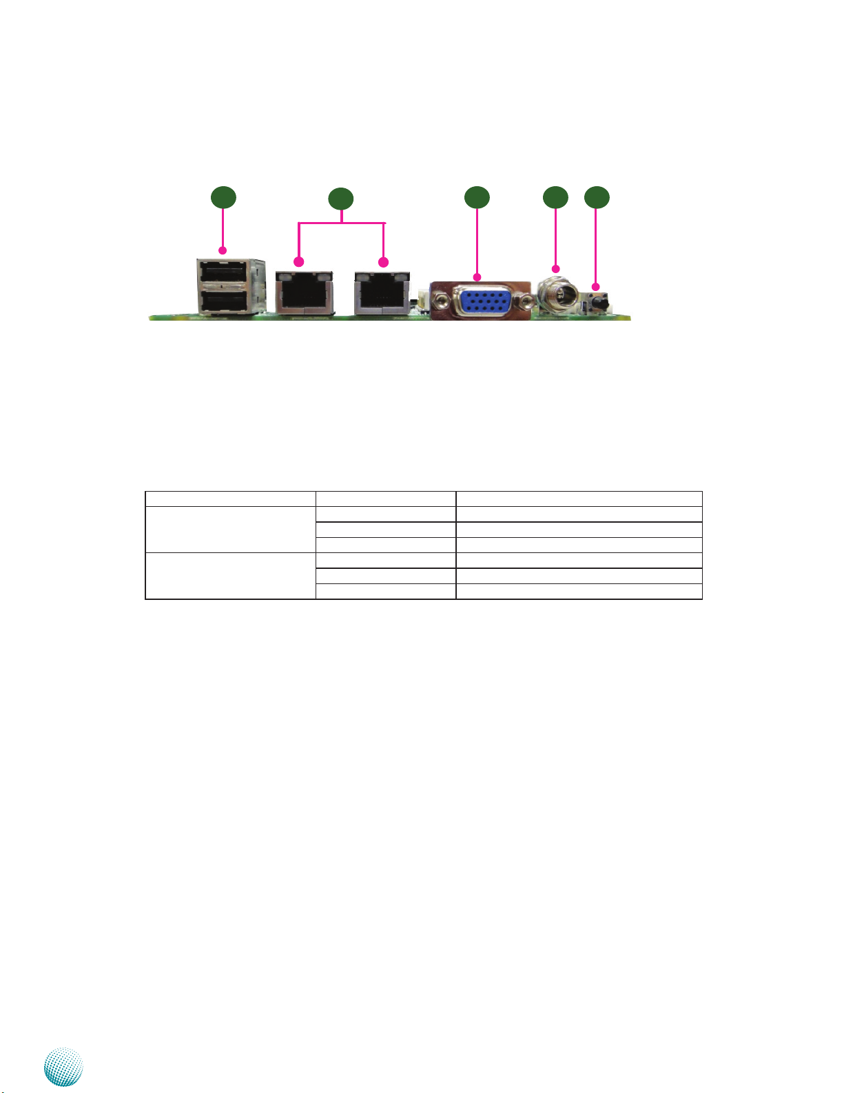
Front Panel Features
Introduction
F2
F1 Two USB 2.0 Ports
It connects to any USB devices such as a flash drive.
F2 Two 10/100/1000Mbps LAN ports: LAN2-left, LAN1-right
Using suitable RJ-45 cable, you can connect VES-310 to a computer, or to any other piece of equipment
that has an Ethernet connection, for example, a hub or a switch. Moreover, both of them have Wakeon-LAN and Preboot Execution Environment capabilities.
LED Behavior Interpretation
LINK/ACT (Left, Yellow) On/Flashing The port is linking.
O The port is not linking.
SPEED (Right, Green/Amber) Amber The connection speed is 1000Mbps.
Green The connection speed is 100Mbps.
O The connection speed is 10Mbps.
F3F1 F5
F4
F3 VGA Port
It is a DB-15 Female ConnectorUsing suitable DB-15 cable, you can connect an appropriate device such
as a monitor.
F4 Power Adapter socket with Lock
DC-in 12V jack. Only use the power adapter supplied with the VES-310 System.
F5 Power-on Switch
It is a switch to turn on or off the power.
Embedded and Industrial Computing
3
Page 6

Chapter 3
LEB-7110
VES-310
Realtek ALC888
DDRII 533/667 MHz
1x SO-DIMM up to 2GB
GbE Controller
2x RTL 8111D
SPI ROM
Processor
Intel
Pineview M SC
Pineview D DC
(BGA)
Intel
ICH8M
Winbond
Super I/O
W83627THG
2x PCIe
HD
Audio
X4 DMI
VGA
LVDS
SATA Connector
Mini PCIe
USB 2.0
2x Port-A
2x Pin Header
Serial Port
COM1: RS232/422/485
COM2: RS232
Parallel Connector
LVDS
18bit
U
A
R
T
SATA
PCIe 3
USB
USB
LAN 1
WOL/PXE
LAN 2
WOL/PXE
Digital I/O
4x in, 4x out
Line-out
MIC-in
Keyboard/Mouse
Chapter 3:
Motherboard Information
Block Diagram
The block diagram depicts the relationships among the
interfaces or modules on the motherboard. Please refer
to the following figure for your motherboard’s layout
design.
Motherboard Information
Embedded and Industrial Computing
4
Page 7

Chapter 3
Board Dimension
The following diagram shows the physical dimension of
the PCB board. (unit: mm)
Motherboard Information
Embedded and Industrial Computing
5
Page 8

Chapter 3
Motherboard Layout- Top View
The motherboard layout shows the connectors and
jumpers on the board. Refer to the following picture
as a reference of the pin assignments and the internal
connectors.
VGA1
Motherboard Information
DCIN1
MPCIE1
LVDS1
J2
VLCD1
PSBTN1
DCJK1
LANB1
LANB2
USBA1
SOUND1
SATA1
PS4S1
FAN1
DIO1
INVER1
Embedded and Industrial Computing
COMB2
COMB1
CMOS
J1
USBB1
PKMA1
SPI-ROM1
LPC1
LPTA1
SC1T3
SC1T2
SC1T1
6
Page 9

Chapter 3
Motherboard Layout-Bottom View with
SO-DIMMS and CF Slot
Motherboard Information
SODIMM1
CF1
Embedded and Industrial Computing
7
Page 10

Chapter 3
Motherboard Information
Jumper Settings
Clear CMOS jumper (CMOS1): It is for clearing the
CMOS memory.
Pin No. Function
1 2 3
Panel Voltage Selector (VLCD1): Use this jumper to
adjust the 5-pin LCD inverter power output.
3
2
1
4-pin Reset or Power-on Push Button (PSBTN1):
This button can be pushed to power up or reset the
system depending on the jumper setting (J2).
2
4
1
3
PSBTN1 Jumper Selection (J2): It is used for selecting
the PSBTN1 push button’s function.
3
2
1
RS-232 COM Port(COMB1, assigned as
COM1): It is for connecting the RS-232 serial port inter-
face cable. It also supports RS-422 and RS-485 communication protocols.
Pin No. Function PIN No. Function
1
9
10
8
6
4
2
Data Carrier Detect (DCD#) 6 Clear to Send (CTS#)
7
2
5
3
1
Data Set Ready (DSR#) 7 Data Terminal Ready (DTR #)
3
Receive Data (RXD) 8 Ring Indicator (RI#)
4
Request to Send (RTS#) 9 Ground
5
Transmit Data (TXD) 10 Key
Pin No. RS-422 Pin
1 422TX2 422TX+
3 422RX+
4 422RX-
RS-232 COM Port(COMB2, assigned as
COM2): It is for connecting the RS-232 serial port inter-
face cable. Unlike COMB1, it only supports RS-232 communication protocol.
Pin No. Function PIN No. Function
1
10
8
6
4
2
Data Carrier Detect (DCD#)
9
7
2
5
3
1
Data Set Ready (DSR#)
3
Receive Data (RXD)
4
Request to Send (RTS#)
5
Transmit Data (TXD) 10
1-2 Normal (Default)
2-3 Clear CMOS
Pin No. Panel Voltage
1-2 +3.3V (Default)
2-3 +5V
Pin No. Panel Voltage
1 Reset Signal
2 GND
3 GND
4 GND
Pin No. Panel Voltage
1-2 +3.3V (Default)
2-3 +5V
Defi nition
Pin No. RS-485 Pin
6
7
8
9
Defi nition
1
2
Data Terminal Ready (DTR #)
DATA-
DATA+
Clear to Send (CTS#)
Ring Indicator (RI#)
Ground
Key
COM1 Type Jumper Selection (SC1T1/SC1T2):
Use jumpers SC1T1 and SC1T2 to select the COM1
communication type.
Jumper
COM1 Type
RS-232 (default) 1-2 1-5,2-6,3-7,4-8
RS-422 3-4 5-9,6-10,7-11,8-12
RS-485 5-6 5-9,6-10,7-11,8-12
SC1T1 SC1T2
Ring-indicator Jumper Setting (SC1T3): The Ring
indicator pinout of the RS-232 COM port (COMB1) can be
altered according to the following jumper settings.
2 4 6
1 3 5
Pin No. Function
5-6 RS-232 Ring (default)
3-4 Supply +12V to Device
1-2 Supply +5V to Device
VGA Interface Connector (VGA1): It is for
connecting the VGA interface cable (2x6 to female
DB15). The VGA is provided by the integrated GPU which
implements Intel® Graphics Media Accelerator 3150 which
supports the following features:
DirectX 9.0c Support: •
MPEG2 Decode capability in Hardware •
Dual Independent Display of VGA and LVDS •
Intel® Dynamic Video Memory Technology 4.0 •
support
-Integrated single LVDS channel support resolution
up to 1280x800 or 1366x768
-Analog RGB display output up to resolution
1400x1050@60Hz
Directx* 9 compliant Pixel Shader* v2.0 •
Intel • ® Clear Video Technology equipped including
MPEG2 Hardware Acceleration and ProcAmp
Development software support including OpenGL* •
1.5 with Microsoft* Windows* and OpenGL* 2.0 with
Linux
SATA Connector (SATA1): It is for connecting a 2.5’’
SATA harddisk to be served as your system’s storage.
Pin No. RS-422 Pin
Defi nition
1 GND
2 TX+
3 TX4 GND
5 RX6 RX+
7 GND
1
2
3
4
5
6
7
Embedded and Industrial Computing
8
Page 11

Chapter 3
52 2
51 1
52 2
51 1
Motherboard Information
4-pin SATA Power Connector (PS4S1): It is used for
connectig the SATA power cord.
4
3
2
1
CF1: Compact Flash Connector (CF1): The
CompactFlash card slot is a type II connector and can be
inserted with type I or II CF card.
Pin NO.. Function Pin NO. Function
1 GND 26 CD12 DATA3 27 DATA11
3 DATA4 28 DATA12
4 DATA5 29 DATA13
5 DATA6 30 DATA14
6 DATA7 31 DATA15
7 CE1# 32 CE2#
8 A10 33 VS1#
9 OE# 34 IOR#
10 A9 35 IOW#
11 A8 36 WE#
12 A7 37 READY#
13 CFVCC3 38 CFVCC3
14 A6 39 CSEL
15 A5 40 VS2#
16 A4 41 RESET
17 A3 42 WAIT#
18 A2 43 INPACK#
19 A1 44 REG#
20 A0 45 DASP#
21 DATA0 46 DIAG#
22 DATA1 47 DATA8
23 DATA2 48 DATA9
24 WP 49 DATA10
25 CD2- 50 GND
FAN Connector (FAN1): The 3-pin connector is for
connecting the system fan.
3
2
1
PS/2 Keyboard and Mouse Connector (PKMA1): It
is for connecting the PS/2 keyboard and mouse interface
cable.
Pin No. Pin Name
1 KBCLK
3 KEY
5 KEY
7 MSCLK
Embedded and Industrial Computing
PIN NO. 1 2 3 4
Function +12V GND GND +5V
50 26
25 1
Function Ground +12V Fan1 Status
PIN NO. 1 2 3
1
3
5
7
Pin No. Pin Name
2
2 GND
4
4 KBDATA
6
6 MSDATA
8
8 +5VS
5-pin LCD (liquid-crystal display) inverter (INVER1):
It can be connected to supply the power to provide a
backlight to the monitor, thus enabling the user to view
what’s on the screen.
PIN NO. Function
1 +12V
2 +12V
3 +5V
4 Backlight Enable
5 GND
LVDS Connector (LVDS1): It is a 1-channel 18bits
LVDS connector.
30 2
29 1
PIN NO. Function PIN NO. Function
1 VCC_LVDS 16 NC
2 VCC_LVDS 17 GND
3 VCC_LVDS 18 NC
4 VCC_LVDS 19 LCDAD1
5 VCC_LVDS 20 NC
6 VCC_LVDS 21 LCDAD1#
7 Reserve( SCL1) 22 NC
8 Reserve( SCL) 23 GND
9 Reserve( SDA1) 24 NC
10 Reserve( SDA) 25 LCDAD2
11 GND 26 LVD_A_CLK
12 NC 27 LCDAD2#
13 LCDAD0 28 LVD_A_CLK#
14 NC 29 GND
15 LCDAD0# 30 GND
Sound Interface Connector (SOUND1): It is provided
by the Realtek ALC888 HD audio codec. It supports Linein/Line-out with 2 channels of independent stereo sound
and microphone input.
1
3
5
7
9
PIN NO. Function PIN NO. Function
1 LOT-R 2 LOT-L
2 CO_GND 4 CO_GND
3 LIN-R 6 LIN-L
4 MIC-R 8 KEY
5 MIC-L 10 CO_GND
2
4
6
8
10
9
Page 12

Chapter 3
Motherboard Information
DIO Output Pin (J10): The 8 pins of Digital Input/
Output (DIO) provide connectors for digital input and
output for controlling digital I/O devices.
10
8
6
4
2
9
Pin No. Pin Name Pin NO. Pin Name
1 Input1 6 Output3
7
2 output1 7 Input4
5
3 Input2 8 Output4
3
4 Output2 9 GND
1
5 Input3 10 VCC5
SO-DIMM Connector (SO-DIMM1): The 200-PIN
DDR2 SO-DIMM connector supports connection of DDR2
667 MHz system memory with a maximum of 2GB.
Mini-PCIe 1X Connector (MPCIE1): It is for
connecting the PCI Express Mini Card such as the wireless
LAN module. The supporting the PCI Express Base
Specification, Revision 1.1.
PIN NO. Description PIN
Description
NO.
1 WAKE# 2 3.3V
3 RSV1 4 GND
5 RSV2 6 1.5V
7 CLKREQ# 8 UIM_PWR
9 GND 10 UIM_DATA
11 REFCLK- 12 UIM_CLK
13 REFCLK+ 14 UIM_RESET
15 GND3 16 UIM_VPP
KEY KEY
17 RSV3 18 GND
19 RSV4 20 W_EISABLE#
21 GND5 22 PERST#
23 PERn0 24 +3.3Vaux
25 PERp0 26 GND
27 GND 28 +1.5V
29 GND 30 SMB_CLK
31 PETn0 32 SMB_DATA
33 PETp0 34 GND
35 GND 36 USB_D37 RSV5 38 USB_D+
39 RSV6 40 GND
41 RSV7 42 LED_WWAN#
43 RSV8 44 LED_WLAN#
45 RSV9 46 LED_WPAN#
47 RSV10 48 +1.5V
49 RSV11 50 GND
51 RSV12 52 +3.3V
12V DC-IN Power Connector (DCJK1): The device
offers two types of power connector which are 12V DCin Jack and 4-pin Connector for ATX mode power supply
(listed below).
Pin No. Pin Name
1 +12V DC-IN
2 GND
3 GND
+12V DC-IN Power Socket for ATX Mode Power
Supply (DCIN1)
Pin No. Pin Name
1 +12V DC-IN
2 GND
3 GND
4 +12V DC-IN
Parallel Connector (LPTA1): The parallel connector
is for connecting parallel port interface cable.
2 26
1 25
Pin No. Pin Name PIN NO. PIN Name
1 Strobe # 2 Auto Form Feed
3 Data0 4 Error #
5 Data1 6 Initialize #
7 Data2 8 Printer Select IN #
9 Data3 10 Ground
11 Data4 12 Ground
13 Data5 14 Ground
15 Data6 16 Ground
17 Data7 18 Ground
19 Acknowledge # 20 Ground
21 Busy 22 Ground
23 Paper Empty 24 Ground
25 Printer Select 26 Key
Dual USB 2.0 Ports (USBB1): Besides the 2 external
USB type A connectors, the internal pin headers for
connecting USB interface cable for additional 2 USB ports
are also provided.
2 10
1 9
Embedded and Industrial Computing
Pin No. Pin Name PIN NO. PIN Name
1 USB3_VCC 2 Ground
3 Key 4 USBD3+
5 USBD2- 6 USBD37 USBD2+ 8 Key
9 Ground 10 USB4_VCC
10
Page 13

Chapter 3
Additional Front Panel LED Connectors (J1): Theses
pin headers can be used as a backup for the following
functions: Hard disk LED, Reset Button, and Power LED
indicator. The front panel already provides access to some
of these functions.
Pin No. Description Pin Name PIN NO. Description Pin Name
1 HDD LED HDD_LED+ 2 Power LED PWR_LED+
3 HDD_LED- 4 PWR_LED-(GND)
5 Reset Button GND 6 Power-on Push Button GND
7 Sys_Reset- 8 PWR_BTN-
9 NC NC 10 PWR_BTN
SPI-ROM Update Connector (J3): Using the
appropriate cable to connect this 10-pin ISP pin header
connector, the user can update the SPI Flash soldered on
board.
Motherboard Information
10
8
6
4
2
Pin NO. Pin Name Pin No. Pin Name
9
1 NC 2 NC
7
3 SPI_CS0 4 V_3P3_SPI
5
5 SPI_ICH_MISO 6 SPI_HOLD0_L
3
7 KEY 8 SPI_ICH_CLK
9 GND 10 SPI_ICH_MOSI
1
LPC I/O bus (Port 80 output for Debug Card) (J4): It
is Intel proprietary connector for connecting a checkpoint
device to output checkpoints throughout Power-On self
test (POST) routine to indicate the task the system is
currently executing.
10
8
6
4
2
Pin NO. Pin Name Pin No. Pin Name
1 CLK_33M_P80 2 LPC_LAD1
3 RST_80DGPT_N 4 LPC_LAD0
5 LPC_FRAME_N 6 +3.3V
7 LPC_AD3 8 GND
9 LPC_AD2 10 GND
9
7
5
3
1
Embedded and Industrial Computing
11
Page 14

Appendix E
Terms and Conditions
Appendix E:
Terms and Conditions
Warranty Policy
All products are under warranty against defects in 1.
materials and workmanship for a period of one year
from the date of purchase.
The buyer will bear the return freight charges for 2.
goods returned for repair within the warranty period;
whereas the manufacturer will bear the after service
freight charges for goods returned to the user.
The buyer will pay for repair (for replaced components 3.
plus service time) and transportation charges (both
ways) for items after the expiration of the warranty
period.
If the RMA Service Request Form does not meet the 4.
stated requirement as listed on “RMA Service,” RMA
goods will be returned at customer’s expense.
The following conditions are excluded from this 5.
warranty:
RMA Service
Requesting a RMA#
To obtain a RMA number, simply fill out and fax the 6.
“RMA Request Form” to your supplier.
The customer is required to fill out the problem code 7.
as listed. If your problem is not among the codes listed,
please write the symptom description in the remarks
box.
Ship the defective unit(s) on freight prepaid terms. 8.
Use the original packing materials when possible.
Mark the RMA# clearly on the box. 9.
Note: Customer is responsible for shipping
damage(s) resulting from inadequate/loose
packing of the defective unit(s). All RMA# are valid
for 30 days only; RMA goods received after the
effective RMA# period will be rejected.
Improper or inadequate maintenance by the •
customer
Unauthorized modification, misuse, or reversed •
engineering of the product.
Operation outside of the environmental specifications •
for the product.
Embedded and Industrial Computing
12
Page 15

Appendix E
RMA Service Request Form
When requesting RMA service, please fill out the following form. Without
this form enclosed, your RMA cannot be processed.
RMA No:
Reasons to Return: Ŀ Repair(Please include failure details)
Ŀ Testing Purpose
Company: Contact Person:
Phone No. Purchased Date:
Fax No.: Applied Date:
Return Shipping Address:
Shipping by: Ŀ Air Freight Ŀ Sea Ŀ Express ___
Ŀ Others:________________
Item Model Name Serial Number Configuration
Item Problem Code Failure Status
*Problem Code:
01:D.O.A.
02: Second Time
R.M.A.
03: CMOS Data Lost
04: FDC Fail
05: HDC Fail
06: Bad Slot
07: BIOS Problem
08: Keyboard Controller Fail
09: Cache RMA Problem
10: Memory Socket Bad
11: Hang Up Software
12: Out Look Damage
13: SCSI
14: LPT Port
15: PS2
16: LAN
17: COM Port
18: Watchdog Timer
19: DIO
20: Buzzer
21: Shut Down
22: Panel Fail
23: CRT Fail
24: Others (Pls specify)
Request Party
Confirmed By Supplier
Authorized Signature / Date Authorized Signature / Date
Terms and Conditions
Embedded and Industrial Computing
13
 Loading...