

Page 1

Embedded &
Industrial Computing
Hardware Platforms for Embedded and Industrial Computing
VES-270
V1.0
>>
User's Manual
Publication date:2014-05-14
Page 2
About
About
Overview
Icon Descriptions
The icons are used in the manual to serve as an indication
of interest topics or important messages. Below is a
description of these icons:
NOTE: This check mark indicates that
there is a note of interest and is something
that you should pay special attention to
while using the product.
Online Resources
The listed websites are links to the on-line product
information and technical support.
Resource Website
Lanner http://www.lannerinc.com
Product Resources
RMA http://eRMA.lannerinc.com
WARNING: This exclamation point
indicates that there is a caution or
warning and it is something that could
damage your property or product.
http://www.lannerinc.com/
download-center/
Acknowledgement
Intel, Pentium and Celeron are registered trademarks of
Intel Corp.
Microsoft Windows and MS-DOS are registered trademarks
of Microsoft Corp.
All other product names or trademarks are properties of
their respective owners.
Compliances and Certification
CE Certication
This product has passed the CE test for environmental
specifications. Test conditions for passing included the
equipment being operated within an industrial enclosure.
In order to protect the product from being damaged by
ESD (Electrostatic Discharge) and EMI leakage, we strongly
recommend the use of CE-compliant industrial enclosure
products.
FCC Class A Certication
This equipment has been tested and found to comply
with the limits for a Class A digital device, pursuant to Part
15 of the FCC Rules. These limits are designed to provide
reasonable protection against harmful interference when
the equipment is operated in a commercial environment.
This equipment generates, uses and can radiate radio
frequency energy and, if not installed and used in
accordance with the instruction manual, may cause
harmful interference to radio communications. Operation
of this equipment in a residential area is likely to cause
harmful interference in which case the user will be required
to correct the interference at his own expense.
Copyright and Trademarks
This document is copyrighted, © 2014. All rights are
reserved. The original manufacturer reserves the right to
make improvements to the products described in this
manual at any time without notice.
No part of this manual may be reproduced, copied,
translated or transmitted in any form or by any means
without the prior written permission of the original
manufacturer. Information provided in this manual is
intended to be accurate and reliable. However, the original
manufacturer assumes no responsibility for its use, nor for
any infringements upon the rights of third parties that
may result from such use.
Embedded and Industrial Computing
2
Page 3

TTaTTable of Contentsbeable of Contents
Chapter 1: Introduction 4
System Specication . . . . . . . . . . . . . . . . . . . . . . . . . . . . . . . . . . . . . . . . . . . 4
Package Contents . . . . . . . . . . . . . . . . . . . . . . . . . . . . . . . . . . . . . . . . . . . . . 5
Chapter 2: System Components 6
System Drawing . . . . . . . . . . . . . . . . . . . . . . . . . . . . . . . . . . . . . . . . . . . . . . 6
Block Diagram: The MainBoard . . . . . . . . . . . . . . . . . . . . . . . . . . . . . . . . . . . . . 8
Chapter 3: Board Layout 9
Motherboard Layout- Top View. . . . . . . . . . . . . . . . . . . . . . . . . . . . . . . . . . . . . 9
Motherboard Layout-Bottom View . . . . . . . . . . . . . . . . . . . . . . . . . . . . . . . . . .10
Connectors and Jumpers List. . . . . . . . . . . . . . . . . . . . . . . . . . . . . . . . . . . . . .11
Jumper Settings . . . . . . . . . . . . . . . . . . . . . . . . . . . . . . . . . . . . . . . . . . . . . .12
Chapter 4: Active Displays Support 17
Appendix A: Terms and Conditions 18
Warranty Policy . . . . . . . . . . . . . . . . . . . . . . . . . . . . . . . . . . . . . . . . . . . .18
RMA Service . . . . . . . . . . . . . . . . . . . . . . . . . . . . . . . . . . . . . . . . . . . . . .18
3
Page 4
Chapter 1
Introduction
Chapter 1:
Introduction
Thank you for choosing the VES-270. The VES-270 is
Lanner’s flagship COM Express R2.0 Type 6 module.
It features the new Core i7/i3 processors with QM77
chipset.
This COM Express module provides a rich I/O capabilities
via high-bandwidth interfaces such as PCI Express, Serial
ATA 2.0/3.0, and Hi-Speed USB 2.0/3.0 connectivity.
Other I/O capabilities include general-purpose I/O
(GPIO), SMbus, and displays supporting LVDS, HDMI, DVI
and DisplayPort as well as Intel® 82579LM (PHY) Gigabit
Ethernet.
System Specification
System
CPU Intel® Core™ i7 / i3 (FCBGA 1023) Processors
BIOS AMI 64Mbit SPI BIOS
System Chipset Intel® QM77 Express Chipset
System Memory
Expansion 7 PCIe x1, 1 PCIe x16
MIO 4 SATA ports, SMbus
USB 8 x USB 2.0, 4 x USB 3.0
DIO 4-bit GPI and 4-bit GPO
Chipset Intel® QM77 Chipset Integrated
Memory DVMT 5.0 Up to 512 MB
Resolution
Display Supported HDMI, DVI, DisplayPort
LVDS Interface Dual-channel 18/ 24-bit LVDS
Chipset Intel® QM77 Integrated
Interface Intel® High Denition Audio
LAN Chip Intel® 82579LM (PHY) Gigabit Ethernet
Ethernet Interface 10/ 100/ 1000 Base-Tx Gigabit Ethernet Compatible
Power Requirement +9 ~ +19 V
ACPI
Power Type AT / ATX
Operating Temperature 0 ~ 60°C (32 ~ 140°F)
Storage Temperature -40 ~ 75°C (-40 ~ 167°F)
Operating Humidity 0% ~ 90% Relative Humidity, Non-condensing
Size (L x W) 125 mm x 95 mm (5” x 3.7”)
Weight 0.2 kg (0.44 lbs)
Two 204-pin DDR3 SODIMM Sockets, Supports Up to
16GB DDR3 1333/ 1600 SDRAM
I/O
Display
CRT Mode: 2048 x 1536
LCD / Simultaneous Mode: 1920 x 1200
Audio Interface
Ethernet
Mechanical & Environmental
Single Power ATX Support S0, S3, S4, S5, ACPI 3.0
Compliant
Embedded and Industrial Computing
Ordering Information
VES-270-7A COM Express® R2.0 Type 6 Module with Intel® CoreTM i7-
VES-270-3A
3517UE CPU and QM77 Chipset
COM Express® R2.0 Type 6 Module with Intel® Core
3120ME CPU and QM77 Chipset
TM
i3-
4
Page 5

Chapter 1
Package Contents
Your package contains the following items:
VES-270 Embedded Board •
Drivers and User’s Manual CD •
Introduction
Embedded and Industrial Computing
5
Page 6
Chapter 2
Chapter 2:
System Components
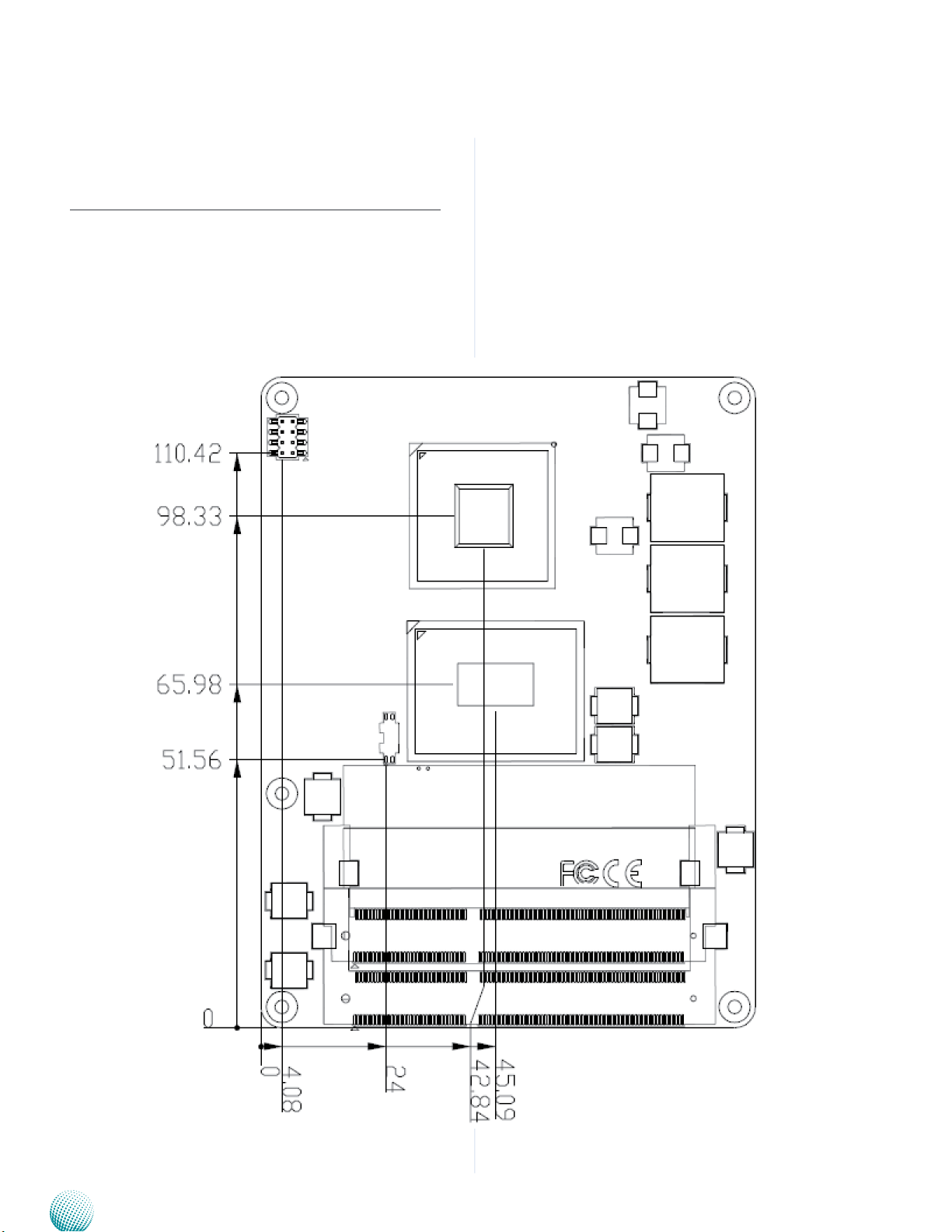
System Drawing
Mechanical dimensions of the VES-270.
Unit: mm
System Components
Embedded and Industrial Computing
6
Page 7

Chapter 2
System Components
Embedded and Industrial Computing
7
Page 8

Chapter 2
QM77
Ivy Bridge
DDR III
SODIMM B
DDR3_B (1600)
6 PCIex1
DMI
DDR3_A (1600)
PCIex1
Giga LAN
PHY
82579LM
4 SATA
HD AUDIO
LVDS 24bitX2
CRT
FDI
DDR III
SODIMM A
8 USB2.0
LPC BUS
SM BUS
TPM Module
NPCT420AA0WX
HW Monitor
NCT7904D
Smart Fan
SPI BUS
SPI
Flash
COMExpress
Connect
Row A,B
PCIeX16
PCIex1
DDP_B
DDP_C
DDP_D
USB3.0 x 4
COMExpress
Connect
Row C,D
Block Diagram: The MainBoard
The block diagram depicts the relationships among the
interfaces and modules on the motherboard.
System Components
Embedded and Industrial Computing
8
Page 9

Chapter 3
Chapter 3:
Board Layout
Motherboard Layout- Top View
The motherboard layout shows the connectors and
jumpers on the board. Refer to the following picture
as a reference of the pin assignments and the internal
connectors.
JSPI1
Motherboard Information
SW1
SODIMM1
SODIMM2
Embedded and Industrial Computing
9
Page 10

Chapter 3
Motherboard Layout-Bottom View
Motherboard Information
CN1A
CN1B
Embedded and Industrial Computing
10
Page 11

Chapter 3
Motherboard Information
Connectors and Jumpers List
The tables below list the function of each of the board
jumpers and connectors by labels shown in the above
section. The next section in this chapter gives pin
definitions and instructions on setting jumpers.
Table 3.1 Connector List for VES-270
Labels Function Pin Denition Reference Page
CN1A
CN1B
JSPI1
SW1
COM Express Connector 1
COM Express Connector 2
Serial Peripheral Interface
AT/ATX Mode Selector
P13
P16
Reserved for Factory Use
P12
Embedded and Industrial Computing
11
Page 12

Chapter 3
52 2
51 1
Motherboard Information
Jumper Settings
AT/ATX Mode Selector (SW1): It is for selecting the
power supply between AT and ATX mode.
AT Mode
COM Express Connector 1 (CN1A)
B110 B1
Signal PIN PIN Signal
GND A1 B1 GND
GBE0_MDI3- A2 B2 GBE0_ACT#
GBE0_MDI3+ A3 B3 LPC_FRAME#
GBE0_LINK100# A4 B4 LPC_AD0
GBE0_LINK1000# A5 B5 LPC_AD1
GBE0_MDI2- A6 B6 LPC_AD2
GBE0_MDI2+ A7 B7 LPC_AD3
GBE0_LINK# A8 B8 LPC_DRQ0#
GBE0_MDI1- A9 B9 LPC_DRQ1#
GBE0_MDI1+ A10 B10 LPC_CLK
GND A11 B11 GND
GBE0_MDI0- A12 B12 PWRBTN#
GBE0_MDI0+ A13 B13 SMB_CK
GBE0_CTREF A14 B14 SMB_DAT
SUS_S3# A15 B15 SMB_ALERT#
SATA0_TX+ A16 B16 SATA1_TX+
SATA0_TX- A17 B17 SATA1_TXSUS_S4# A18 B18 SUS_STAT#
SATA0_RX+ A19 B19 SATA1_RX+
SATA0_RX- A20 B20 SATA1_RXGND A21 B21 GND
SATA2_TX+ A22 B22 SATA3_TX+
SATA2_TX- A23 B23 SATA3_TXSUS_S5# A24 B24 PWR_OK
SATA2_RX+ A25 B25 SATA3_RX+
SATA2_RX- A26 B26 SATA3_RXBATLOW# A27 B27 WDT
(S)ATA_ACT# A28 B28 AC/HDA_SDIN2
AC/HDA_SYNC A29 B29 AC/HDA_SDIN1
AC/HDA_RST# A30 B30 AC/HDA_SDIN0
Embedded and Industrial Computing
Pin No. Function
1 On 2 On AT mode: This mode
1 Off 2 On ATX mode:This mode
ATX
Mode
A110 A1
supports AT power
supply; there is no
need to press power
button to enable
power on/off.
supports ATX power
supply. Press the ATX
power button to enable power on/off.
Signal PIN PIN Signal
GND A31 B31 GND
AC/HDA_BITCLK A32 B32 SPKR
AC/HDA_SDOUT A33 B33 I2C_CK
BIOS_DIS0# A34 B34 I2C_DAT
THRMTRIP# A35 B35 THRM#
USB6- A36 B36 USB7USB6+ A37 B37 USB7+
USB_6_7_OC# A38 B38 USB_4_5_OC#
USB4- A39 B39 USB5USB4+ A40 B40 USB5+
GND A41 B41 GND
USB2- A42 B42 USB3USB2+ A43 B43 USB3+
USB_2_3_OC# A44 B44 USB_0_1_OC#
USB0- A45 B45 USB1USB0+ A46 B46 USB1+
VCC_RTC A47 B47 EXCD1_PERST#
EXCD0_PERST# A48 B48 EXCD1_CPPE#
EXCD0_CPPE# A49 B49 SYS_RESET#
LPC_SERIRQ A50 B50 CB_RESET#
GND A51 B51 GND
PCIE_TX5+ A52 B52 PCIE_RX5+
PCIE_TX5- A53 B53 PCIE_RX5GPI0 A54 B54 GPO1
PCIE_TX4+ A55 B55 PCIE_RX4+
PCIE_TX4- A56 B56 PCIE_RX4GND A57 B57 GPO2
PCIE_TX3+ A58 B58 PCIE_RX3+
PCIE_TX3- A59 B59 PCIE_RX3GND A60 B60 GND
PCIE_TX2+ A61 B61 PCIE_RX2+
PCIE_TX2- A62 B62 PCIE_RX2GPI1 A63 B63 GPO3
PCIE_TX1+ A64 B64 PCIE_RX1+
PCIE_TX1- A65 B65 PCIE_RX1GND A66 B66 WAKE0#
GPI2 A67 B67 WAKE1#
PCIE_TX0+ A68 B68 PCIE_RX0+
PCIE_TX0- A69 B69 PCIE_RX0GND A70 B70 GND
LVDS_A0+ A71 B71 LVDS_B0+
LVDS_A0- A72 B72 LVDS_B0LVDS_A1+ A73 B73 LVDS_B1+
LVDS_A1- A74 B74 LVDS_B1LVDS_A2+ A75 B75 LVDS_B2+
LVDS_A2- A76 B76 LVDS_B2LVDS_VDD_EN A77 B77 LVDS_B3+
LVDS_A3+ A78 B78 LVDS_B3LVDS_A3- A79 B79 LVDS_BKLT_EN
GND A80 B80 GND
LVDS_A_CK+ A81 B81 LVDS_B_CK+
LVDS_A_CK- A82 B82 LVDS_B_CKLVDS_I2C_CK A83 B83 LVDS_BKLT_CTRL
LVDS_I2C_DAT A84 B84 VCC_5V_SBY
GPI3 A85 B85 VCC_5V_SBY
RSVD1 A86 B86 VCC_5V_SBY
RSVD2 A87 B87 VCC_5V_SBY
PCIE_CLK_REF+ A88 B88 BIOS_DIS1#
12
Page 13

Chapter 3
Motherboard Information
Signal PIN PIN Signal
PCIE_CLK_REF-- A89 B89 VGA_RED
GND A90 B90 GND
SPI_POWER A91 B91 VGA_GRN
SPI_MISO A92 B92 VGA_BLU
GPO0 A93 B93 VGA_HSYNC
SPI_CLK A94 B94 VGA_VSYNC
SPI_MOSI A95 B95 VGA_I2C_CK
PP_TPM A96 B96 VGA_I2C_DAT
TYPE10# A97 B97 SPI_CS#
NC A98 B98 NC
NC A99 B99 NC
GND A100 B100 GND
NC A101 B101 FAN_PWMOUT
NC A102 B102 FAN_TACHIN
LID# A103 B103 SLEEP#
VIN A104 B104 VIN
VIN A105 B105 VIN
VIN A106 B106 VIN
VIN A107 B107 VIN
VIN A108 B108 VIN
VIN A109 B109 VIN
GND A110 B110 GND
Signal Description of CN1A:
Audio•
Signal Signal Description
AC/HDA_SYNC HD Audio Sync
AC/HDA _RST# HD Audio Reset
AC/HDA _SDIN[0:2] Audio CODEC Serial Data
AC/HDA _BITCLK HD Audio Clock
AC/HDA _SDOUT HD Audio Data
Gigabit Ethernet Signals•
Signal Signal Description
GBE0_MD[0:3]
+/-
GBE0_ACT# Gigabit Ethernet Controller 0 activity
GBE0_Link# Gigabit Ethernet Controller 0 link indi-
GBE0_Link100# Gigabit Ethernet Controller 0 100 Mbit
GBE0_Lin1000# Gigabit Ethernet Controller 0 1000
GPIO Signals•
Signal Signal Description
GPI[0:4] General purpose input pins.
GPO[0:4] General purpose output pins.
Flat Panel LVDS Signals•
Signal Signal Description
LVDS_BKLT_CTRL LVDS panel backlight brightness
LVDS_VDD_EN LVDS panel power enable.
LVDS_BKLT_EN LVDS panel backlight enable.
2
I
C_DAT, I2C_CLK I2C interface for panel parameter
Gigabit Ethernet Controller 0: Media
Dependent Interface Dierential Pairs
0,1,2,3. The MDI can operate in 1000,
100 and 10 Mbit / sec modes. Some
pairs are unused in some modes, per
the following:
1000B-T 100B-T 10B-T
MDI[0]+/- B1_DA+/ TX+/- TX+/MDI[1]+/ B1_DB+/ RX+/- RX+/MDI[2]+/ B1_DC+/ X X
MDI[3]+/ B1_DD+/ X X
indicator, active low.
cator, active low.
/sec link indicator, active low.
Mbit/sec link indicator, active low.
control.
EEPROM. This EEPROM is mounted
on the LVDS receiver. The data in the
EEPROM allows the EXT module to
automatically set the proper timing
parameters for a specic LCD panel.
Embedded and Industrial Computing
LPC Signals•
Signal Signal Description
LPC_FRAME# LPC frame indicates the start of an LPC
cycle
LPC_AD[0:3] LPC multiplexed address, command
and data bus
LPC_DRQ[0:1]# LPC serial DMA request
LPC_CLK LPC clock output - 33MHz nominal
LPC_SERIRQ LPC serial interrupt
13
Page 14

Chapter 3
Motherboard Information
Miscellaneous Signals•
Signal Signal Description
2
I
C_CK General purpose I2C port clock output
2
I
C_DAT General purpose I2C port data I/O line
SPKR Output for audio enunciator - the
"speaker" in PC-AT systems
BIOS_DIS0#
BIOS_DIS1#
KB_RST# Input to module from (optional) exter-
KB_A20GATE Input to module from (optional) ex-
PCI Express Signals•
Signal Signal Description
PCIE_TX[0:4]
+/PCIE_RX[0:4]
+/PCIE0_CK_
REF+/-
Selection straps to determine the BIOS
boot device
BIOS_
DIS1#
1 1 Module Module
1 0 Module Module
0 1 Module Carrier
0 0 Carrier Module
Carrier
SPI_CS#
High Module SPI0/
High Module Carrier
SPI0 Carrier SPI0/
SPI1 Module SPI0/
nal keyboard controller that can force
a reset.
ternal keyboard controller that can be
used to control the CPU A20 gate line.
PCI Express Dierential Transmit Pair 0-4
PCI Express Dierential Receive Pair 0-4
Reference clock output for PCI Express
lanes 0-7 and for PCI Express Graphics
lanes 0-15
BIOS_
DIS0#
SPI
Descriptor
Chipset
SPI CS1#
Destination
BIOS
Entry
SPI1
FWH
SPI1
SPI1
Chipset
SPI CS0#
Destination
Ref
Line
0
1
2
3
Power Signals•
Signal Signal Description
VCC_5V_SBY Standby power input: +5.0V nominal. If
VCC5_SBY is used, all available VCC_5V_
SBY pins on the connectors must be
used. Only used for standby and suspend
functions. May be left unconnected if
these functions are not used in the system
design.
VCC_RTC Real-time clock circuit-power input. Nomi-
nally +3.0V.
VIN Primary power input: +9V~19V.
Power and System Management Signals•
Signal Signal Description
SUS_S3# Indicates system is in suspend to RAM
state. Active low output.
SUS_S4# Indicates system is in suspend to Disk
state. Active low output.
SUS_S5# Indicates system is in Soft O state.
BATLOW# Indicates that external battery is low
PWRBTN# Power button to bring system out of S5
(soft o), active on falling edge.
SMB_CK System Management Bus bidirectional
clock line.
SMB_DTA System Management Bus bidirectional
data line.
SMB_ALERT# System Management Bus Alert - input
can be used to generate an SMI# (System
Management Interrupt) or to wake the
system.
SUS_STAT# Indicates imminent suspend operation.
PWR_OK Power OK from main power supply
THRMTRIP# Active low output indicating that the CPU
has entered thermal shutdown.
THRM# Input from o-module temp sensor indi-
cating and over-temp situation.
SYS_RESET# Reset button input. Active low input.
WAKE0# PCI Express wake up signal.
WAKE1# General purpose wake up signal.
SATA Signals•
Signal Signal Discription
SATA[0:3]_TX
+/SATA[0:3]_RX
+/ATA_ACT# ATA (parallel and serial) activity indicator,
Serial ATA Channel 0-3 transmit dieren-
tial pair.
Serial ATA Channel 0-3 receive dierential
pair.
active low.
Embedded and Industrial Computing
14
Page 15

Chapter 3
52 2
51 1
Motherboard Information
VGA Signals•
Signal Signal Discription
VGA_RED Red for monitor. Analog DAC output.
VGA_GRN Green for monitor. Analog DAC output.
VGA_BLU Blue for monitor. Analog DAC output.
VGA_HSYNC Horizontal sync output to VGA monitor
VGA_VSYNC Vertical sync output to VGA monitor
2
VGA_ I
VGA_ I
Signal Signal Description
USB[0:7] +/- USB dierential pairs, channels 0 through
USB_0_1_OC# USB over-current sense, USB channels 0
USB_2_3_OC# USB over-current sense, USB channels 2
USB_4_5_OC# USB over-current sense, USB channels 4
USB_6_7_OC# USB over-current sense, USB channels 6
COM Express Connector 2 (CN1B)
GND C1 D1 GND
GND C2 D2 GND
USB_SSRX0- C3 D3 USB_SSTX0USB_SSRX0+ C4 D4 USB_SSTX0+
GND C5 D5 GND
USB_SSRX1- C6 D6 USB_SSTX1USB_SSRX1+ C7 D7 USB_SSTX1+
GND C8 D8 GND
USB_SSRX2- C9 D9 USB_SSTX2USB_SSRX2+ C10 D10 USB_SSTX2+
GND C11 D11 GND
USB_SSRX3- C12 D12 USB_SSTX3USB_SSRX3+ C13 D13 USB_SSTX3+
GND C14 D14 GND
DDI1_PAIR6+ C15 D15 DDI1_CTRLCLK_
DDI1_PAIR6- C16 D16 DDI1_CTRLDATA_
C_CK DDC clock line (I2C port dedicated to
2
C_DAT DDC data line.
USB Signals•
C110 C1
D110 D1
Signal PIN PIN Signal
Embedded and Industrial Computing
identify VGA monitor capabilities)
7
and 1
and 3
and 5
and 7
AUX+
AUX-
Signal PIN PIN Signal
NC C17 D17 NC
NC C18 D18 NC
PCIE_RX6+ C19 D19 PCIE_TX6+
PCIE_RX6- C20 D20 PCIE_TX6GND C21 D21 GND
NC C22 D22 NC
NC C23 D23 NC
DDI1_HPD C24 D24 NC
DDI1_PAIR4+ C25 D25 NC
DDI1_PAIR4- C26 D26 DDI1_PAIR0+
NC C27 D27 DDI1_PAIR0NC C28 D28 NC
DDI1_PAIR5+ C29 D29 DDI1_PAIR1+
DDI1_PAIR5- C30 D30 DDI1_PAIR1GND C31 D31 GND
DDI2_CTRLCLK_
AUX+
DDI2_CTRLDATA_
AUXDDI2_DDC_AUX_
SEL
NC C35 D35 NC
DDI3_CTRLCLK_
AUX+
DDI3_CTRLDATA_
AUXDDI3_DDC_AUX_
SEL
DDI3_PAIR0+ C39 D39 DDI2_PAIR0+
DDI3_PAIR0- C40 D40 DDI2_PAIR0GND C41 D41 GND
DDI3_PAIR1+ C42 D42 DDI2_PAIR1+
DDI3_PAIR1- C43 D43 DDI2_PAIR1DDI3_HPD C44 D44 DDI2_HPD
NC C45 D45 NC
DDI3_PAIR2+ C46 D46 DDI2_PAIR2+
DDI3_PAIR2- C47 D47 DDI2_PAIR2NC C48 D48 NC
DDI3_PAIR3+ C49 D49 DDI2_PAIR3+
DDI3_PAIR3- C50 D50 DDI2_PAIR3GND C51 D51 GND
PEG_RX0+ C52 D52 PEG_TX0+
PEG_RX0- C53 D53 PEG_TX0TYPE0# C54 D54 PEG_LANE_RV#
PEG_RX1- C56 D56 PEG_TX1TYPE1# C57 D57 TYPE2#
PEG_RX2+ C58 D58 PEG_TX2+
PEG_RX2- C59 D59 PEG_TX2GND C60 D60 GND
GND C60 D60 GND
PEG_RX3+ C61 D61 PEG_TX3+
PEG_RX3- C62 D62 PEG_TX3NC C63 D63 NC
NC C64 D64 NCPEG_RX4+ C65 D65 PEG_TX4+
PEG_RX4- C66 D66 PEG_TX4NC C67 D67 GND
C32 D32 DDI1_PAIR2+
C33 D33 DDI1_PAIR2-
C34 D34 DDI1_DDC_AUX_
SEL
C36 D36 DDI1_PAIR3+
C37 D37 DDI1_PAIR3-
C38 D38 NC
15
Page 16

Chapter 3
Motherboard Information
Signal PIN PIN Signal
PEG_RX5+ C68 D68 PEG_TX5+
PEG_RX5- C69 D69 PEG_TX5GND C70 D70 GND
PEG_RX6+ C71 D71 PEG_TX6+
PEG_RX6- C72 D72 PEG_TX6GND C73 D73 GND
PEG_RX7+ C74 D74 PEG_TX7+
PEG_RX7- C75 D75 PEG_TX7GND C76 D76 GND
NC C77 D77 NC
PEG_RX8+ C78 D78 PEG_TX8+
PEG_RX8- C79 D79 PEG_TX8GND C80 D80 GND
PEG_RX9+ C81 D81 PEG_TX9+
PEG_RX9- C82 D82 PEG_TX9NC C83 D83 NC
GND C84 D84 GND
PEG_RX10+ C85 D85 PEG_TX10+
PEG_RX10- C86 D86 PEG_TX10GND C87 D87 GND
PEG_RX11+ C88 D88 PEG_TX11+
PEG_RX11- C89 D89 PEG_TX11GND C90 D90 GND
PEG_RX12+ C91 D91 PEG_TX12+
PEG_RX12- C92 D92 PEG_TX12GND C93 D93 GND
PEG_RX13+ C94 D94 PEG_TX13+
PEG_RX13- C95 D95 PEG_TX13GND C96 D96 GND
NC C97 D97 NC
PEG_RX14+ C98 D98 PEG_TX14+
PEG_RX14- C99 D99 PEG_TX14GND C100 D100 GND
PEG_RX15+ C101 D101 PEG_TX15+
PEG_RX15- C102 D102 PEG_TX15GND C103 D103 GND
VIN C104 D104 VIN
VIN C105 D105 VIN
VIN C106 D106 VIN
VIN C107 D107 VIN
VIN C108 D108 VIN
VIN C109 D109 VIN
GND C110 D110 GND
Signal Signal Description
PEG_TX[ 0:15]+
PEG_TX[ 0:15]PEG_RX[ 0:15]+
PEG_RX[ 0:15]PEG_LANE_RV# PCI Express Graphics lane
DDI Signals•
Signal Signal Description
DDI[1:3]_PAIR[0:3]+
DDI[1:3]_PAIR [0:3]-
DDI[1:3]_DDC_AUX_SEL Selects the function of
DDI[1:3]_CTRLCLK_AUX+ DP AUX+function if
DDI[1:3]_CTRLDATA_AUX- DP AUX-function if
DDI[1:3]_HPD Digital Display Interface
PCI Express Graphics
transmit dierential paris.
PCI Express Graphics
recevie dierential paris.
reversal input strap. Pull
low on the Carrier board
to reverse lane order.
Digital Display Interface
1 to 3 Pair[0:3] dierential
pairs
DDI[1:3]_CTRLCLK_AUX+
and DDI[1:3]_CTRLDATA_
AUX-. If this input is oating
the AUX pair is used for
the DP AUX+/- signals. If
pulled-high the AUX pair
contains the CRTLCLK and
CTRLDATA signals.
DDI[1:3]_DDC_AUX_SEL is
no connect
HDMI/DVI 12C CTRLCLK if
DDI[1:3]_DDC_AUX_SEL is
pulled high
DDI[1:3]_DDC_AUX_SEL is
no connect
HDMI/DVI 12C CTRLDATA if
DDI[1:3]_DDC_AUX_SEL is
pulled high
Hot-Plug Detect
Signal Description of CN1B:
USB Signals•
Signal Signal Description
USB_SSTX[0:3]+
USB_SSTX[0:3]-
USB_SSRX[0:3]+
USB_SSRX[0:3]-
PEG Signals
Embedded and Industrial Computing
Additional transmit signal differential pairs for the SuperSpeed USB data path.
Additional receive signal differential pairs for the SuperSpeed USB data path.
16
Page 17

Chapter 4
Active Displays Support
Chapter 4:
Active Displays Support
QM77 supports 3 Display Digital Ports B, C, D. (DDPB,
DDPC and DDPD):
DDPB: Capable of HDMI/DVI/DisplayPort/SDVO
DDPC: Capable of HDMI/DVI/DisplayPort
DDPD: Capable of HDMI/DisplayPort
Table below lists recommended processors that could be
used for 3 Active Displays Support
Processor codename Graphics
Ivy Bridge Desktop Intel HD Graphics
Ivy Bridge Mobile Intel HD Graphics
Triple Clone: all the three display show the same
contents.
Triple extended: All the three display have independent
content.
Conguration Display 1 Display 2 Display 3
8 DP B DP C HDMI D
9 DP B DP D HDMI C
10 DP C DP D HDMI B
NOTE:
In this display table, display combinations
1.
with dongles are not mentioned. However, DVI or
HDMI can be connected with DPI to DVI dongle
or DP to HDMI dongle respectively.
You need appropriate vBIOS settings for 2.
integrated HDMI/DisplayPort configuration with
external connectors.
Note: This feature is not applicable for Windows
XP.
Due to the hardware design of VES-270 and VES-8X6, the
onboard HDMI interface supported by DDPC and Display
Port is supported by DDPD. DDPB is connected to Digital
Display Interface (DDI), and it could support HDMI/DVI/
DP/SDVO via an add-on adapter card.
The table below lists supported 3 display combinations
on the VES-8X6 carrier board.
Conguration Display 1 Display 2 Display 3
1 CRT DP B DP D
2 LFP DP B DP D
3 DP B HDMI C DP D
Depending on the carrier board design, table below shows
possible supported display combinations
Conguration Display 1 Display 2 Display 3
1 CRT DP B DP C
2 CRT DP C DP D
3 CRT DP B DP D
4 LFP DP C DP D
5 LFP DP B DP D
6 LFP DP B DP C
7 DP B DPC DP D
Embedded and Industrial Computing
17
Page 18

Appendix A
Terms and Conditions
Appendix A:
Terms and Conditions
Warranty Policy
All products are under warranty against defects in 1.
materials and workmanship for a period of one year
from the date of purchase.
The buyer will bear the return freight charges for 2.
goods returned for repair within the warranty period;
whereas the manufacturer will bear the after service
freight charges for goods returned to the user.
The buyer will pay for repair (for replaced components 3.
plus service time) and transportation charges (both
ways) for items after the expiration of the warranty
period.
If the RMA Service Request Form does not meet the 4.
stated requirement as listed on “RMA Service,” RMA
goods will be returned at customer’s expense.
The following conditions are excluded from this 5.
warranty:
RMA Service
Requesting a RMA#
To obtain a RMA number, simply fill out and fax the 1.
“RMA Request Form” to your supplier.
The customer is required to fill out the problem code 2.
as listed. If your problem is not among the codes listed,
please write the symptom description in the remarks
box.
Ship the defective unit(s) on freight prepaid terms. 3.
Use the original packing materials when possible.
Mark the RMA# clearly on the box. 4.
Note: Customer is responsible for shipping
damage(s) resulting from inadequate/loose
packing of the defective unit(s). All RMA# are valid
for 30 days only; RMA goods received after the
effective RMA# period will be rejected.
Improper or inadequate maintenance by the customer
Unauthorized modification, misuse, or reversed
engineering of the product Operation outside of the
environmental specifications for the product.
Embedded and Industrial Computing
18
Page 19

Appendix A
RMA Service Request Form
When requesting RMA service, please fill out the following form. Without
this form enclosed, your RMA cannot be processed.
RMA No:
Reasons to Return: Ŀ Repair(Please include failure details)
Ŀ Testing Purpose
Company: Contact Person:
Phone No. Purchased Date:
Fax No.: Applied Date:
Return Shipping Address:
Shipping by: Ŀ Air Freight Ŀ Sea Ŀ Express ___
Ŀ Others:________________
Item Model Name Serial Number Configuration
Item Problem Code Failure Status
*Problem Code:
01:D.O.A.
02: Second Time
R.M.A.
03: CMOS Data Lost
04: FDC Fail
05: HDC Fail
06: Bad Slot
07: BIOS Problem
08: Keyboard Controller Fail
09: Cache RMA Problem
10: Memory Socket Bad
11: Hang Up Software
12: Out Look Damage
13: SCSI
14: LPT Port
15: PS2
16: LAN
17: COM Port
18: Watchdog Timer
19: DIO
20: Buzzer
21: Shut Down
22: Panel Fail
23: CRT Fail
24: Others (Pls specify)
Request Party
Confirmed By Supplier
Authorized Signature / Date Authorized Signature / Date
Terms and Conditions
Embedded and Industrial Computing
19
 Loading...