

Page 1

In-Vehicle Computing
Hardware Platforms for mobile applications
LVC-5000-B Series
V1.0
User's Manual
Release date: 2014/12/30
Page 2
Overview
Icon Descriptions
The icons are used in the manual to serve as an
indication of interest topics or important messages.
Below is a description of these icons:
NOTE: This check mark indicates
that there is a note of interest and is
something that you should pay special
attention to while using the product.
WARNING: This exclamation point
indicates that there is a caution or
warning and it is something that could
damage your property or product.
Online Resources
The listed websites are links to the on-line product
information and technical support.
Resource Website
Lanner http://www.lannerinc.com
Product Resources http://assist.lannerinc.com
RMA http://eRMA.lannerinc.com
Copyright and Trademarks
This document is copyrighted, © 2014. All rights are
reserved. The original manufacturer reserves the right to
make improvements to the products described in this
manual at any time without notice.
No part of this manual may be reproduced, copied,
translated or transmitted in any form or by any means
without the prior written permission of the original
manufacturer. Information provided in this manual
is intended to be accurate and reliable. However, the
original manufacturer assumes no responsibility for its
use, nor for any infringements upon the rights of third
parties that may result from such use.
Acknowledgement
Intel, Pentium and Celeron are registered trademarks of
Intel Corp.
Microsoft Windows and MS-DOS are registered
trademarks of Microsoft Corp.
All other product names or trademarks are properties of
their respective owners.
Compliances and Certification
CE Certication
This product has passed the CE test for environmental
specifications. Test conditions for passing included
the equipment being operated within an industrial
enclosure. In order to protect the product from being
damaged by ESD (Electrostatic Discharge) and EMI
leakage, we strongly recommend the use of CEcompliant industrial enclosure products.
FCC Class A Certication
This equipment has been tested and found to comply
with the limits for a Class A digital device, pursuant
to Part 15 of the FCC Rules. These limits are designed
to provide reasonable protection against harmful
interference when the equipment is operated in a
commercial environment. This equipment generates,
uses and can radiate radio frequency energy and, if not
installed and used in accordance with the instruction
manual, may cause harmful interference to radio
communications. Operation of this equipment in a
residential area is likely to cause harmful interference
in which case the user will be required to correct the
interference at his own expense.
e Mark Certication
E13 - Luxembourg
Page 3

Mechanical compliance
Vibration:
General Vibration (operating): Refer to MIL-STD-810G, •
Method 514.6, Procedure I (Transportation), Category
4 – Common carrier (US highway truck vibration
exposure)
General Vibration (non-operating): Refer to MIL-STD- •
810G, Method 514.6, Procedure I (Transportation),
Category 24 – General minimal integrity
Shock:
Operating (Functional Test for Ground Equipment): •
Refer to MIL-STD-810G, Method 516.6, Procedure I,
40g, 11ms
Non-Operating (Crash Hazard Shock Test for Ground •
Equipment): Refer to MIL-STD-810G, Method 516.6,
Procedure V, 75g, 11ms
Electrical transient conduction along supply lines only
(12V/24V)
Revision History
Version Date Description
1.0 2014/12/30 Ofcial release
Page 4

Chapter 1: Introduction 5
Model Summaries 5
System Specifications 6
Package Contents 6
Chapter 2: System Components 7
System Drawing 7
Block Diagram: The MainBoard 9
Front Components 12
Rear Components 13
Chapter 3: Motherboard Information 15
Inside LVC-5000-B Series 15
Jumpers & Connectors on the Motherboard 18
Jumpers & Connectors on the Motherboard 20
Jumpers & Connectors on the PoE Power Board 21
Jumpers & Connectors on the Add-on Card LVK-CBPE1 22
Jumpers & Connectors on the Add-on Card LVK-CBSA1 23
Connectors and Jumpers List 24
Jumper Settings & Connector Pinouts 25
Chapter 4: Hardware Setup 36
Preparing the Hardware Installation 36
Installing a CompactFlash Card 36
SIM Card Installation 36
Installing a HDD/SSD Disk Drive 36
Mini-PCIe Wireless Network Module Installation 37
Connecting Power 38
Chapter 5: The Flow Chart 39
Appendix A: Using the Ignition System Manager (ISM) 40
Appendix B: Digital Input/Output 41
Appendix C: Accessing the Digital Accelerometer Data 47
Appendix D: Accessing the GPS Data 48
Appendix E: Programming System Watchdog Timer 50
Appendix F: Terms and Conditions 54
Table of Contents
Page 5

Chapter 1:
Introduction
Thank you for choosing Lanner LVC-5000-B series. The
LVC-5000-B series is a rugged vehicle PC designed
to be integrated on-board for eet management
applications and vehicle monitoring.
The system encompasses a wide variety of
communication ports to facilitate every possible invehicle applications including surveillance, event data
recorder and the GPS receiver. It also features an
external HDD/SSD drive bay for easy storage device access
and replacement.
Intel® Celeron® 847E 1.1GHz / Core™ i7-3517UE •
1.7GHz
Supports DDR3 SO-DIMM memory, pre-installed •
with 4GB SO-DIMM module by default
Support DVI-D+VGA, DVI-D+HDMI, HDMI+VGA •
independent display interface.
2x mini-PCIe sockets to support WiFi and 3G wireless •
connection
Externally accessible 2.5” SATA HDD/SSD drive bay, •
CompactFlash and SIM card installation.
Support 12V DC output @Max 1A•
Onboard Ublox NEO-6Q GPS receiver module•
Supports 4 Ports PoE •
Suspension kit for anti-vibration•
1x RS232 & 1x RS232/422/485, support RI/5V/12V •
selection with relay output @Max 2A
Model Summaries
LVC-5000-B0 (4 POEs):
1.7 GHz Intel® Core™ i7-3517UE In-Vehicle Mobile
NVR, DDR3 4GB SO-DIMM x1, 2.5” external Drive
Bay x1(support to TB grade HDD), Mini-PCIe x2 with
2 external accessible SIM card reader, Intel GbE x4
support PoE, USB x4, RS232/422/485 x1, RS232
x1, CF x1, Multi-I/O, Audio, HDMI, VGA, DVI, DC
Power input +9~36Vdc with Ignition, Suspending Kit
included.
LVC-5000-B1/B2 (LVK-CBPE1 add-on card + 4 POEs):
1.1 GHz Intel® Celeron® 847E/ 1.7 GHz Intel®
Core™ i7-3517UE In-Vehicle Mobile NVR, DDR3
4GB SO-DIMM x1, 2.5” external Drive Bay x1, MiniPCIe x2 with 2 external accessible SIM card reader,
Intel GbE x4 support PoE, USB x4, RS232/422/485
x1, RS232 x1, CF x1, Multi-I/O, Audio, HDMI, VGA,
DVI, Support CAN Bus Module MT3647 & MT1200,
extra Mini-PCIe x1 with SIM card reader, DC Power
input +9~36Vdc with Ignition, Suspending Kit
included.
LVC-5000-B3 (LVK-CBSA1 + 4 POEs):
1.7 GHz Intel® Core™ i7-3517UE In-Vehicle Mobile
NVR, DDR3 4GB SO-DIMM x1, 2.5” external Drive
Bay x1, Mini-PCIe x2 with 2 external accessible
SIM card reader, Intel GbE x4 support PoE, USB
x4, RS232/422/485 x1, RS232 x1, CF x1, MultiI/O, Audio, HDMI, VGA, DVI, Support CAN Bus
Module MT3647 & MT1200, extra Mini-PCIe x1 with
SATA interface supports mSATA (major InnoDisk_
mSATA_3ME series), DC Power input +9~36Vdc
with Ignition, Suspending Kit included.
Page 6
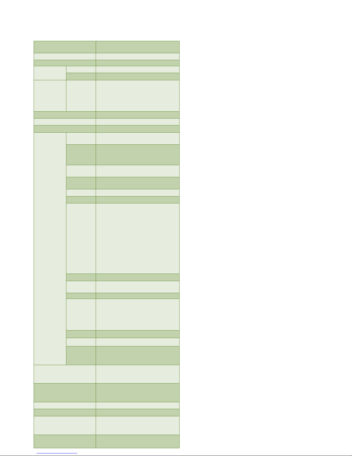
System Specifications
Dimensions (unit: mm)
273.8x188.0x72.0
308.0x188.0x100.6 (w/ suspension kit)
Processor Intel 847E/i7-3517UE
Chipset Intel HM65
System
Memory
Technology DDR3 SO-DIMM x1
(default 4GB)
Max. Capacity Up to 8GB (user option)
Storage SATA & CF
1x 2.5” HDD/SSD drive bay
(up to TB
grade)
1 x CF socket
1 x mSATA storage module socket (B3
model ONLY)
Ethernet Controller Intel 82583V x4
Graphic Controller Intel Integrated HD graphic engine
Audio Controller Realtek ALC886 GR
I/O
LAN
4 x GbE RJ45 w/PoE, IEEE 802.3af
compliant
Display
DVI-D x 1
VGA x 1
HDMI x 1
Audio
Mic-in and Line-out/HD Audio output by
MIO terminal block
Serial COM
1x RS-232 and 1x RS-232/422/485 both
with RI/5V/12V
GPS Ublox NEO-6Q GPS receiver module
G-sensor ADXL 345
MIO
26-pin terminal block for GPIO:
4x DI ( 5V or 12V TTL selectable)
4x DO (12V TTL , Max. 100mA)
2x DO control Relay support 9~36V@
max 2A each
2x DI to Ignition MCU as remote control
( 5V TTL)
Audio MIC input and HD Audio output
(w/2Watt)
COM TX RX, for Ignition Microcontroller
program/service purpose.
USB USB 2.0 Type A x4
Power Input
3-pin terminal block (DC 9~36V, GND
and Ignition)
Power Output 12VDC/1A
Expansion
2 x mini-PCIe sockets USB+SIM (Both
with SIM card readers)
1x full-size mini-PCIexpress socket
(USB+PCIe) with SIM-card reader (except
B0 and B3)
Antenna 7 x SMA-type antenna holes
CAN bus Available in B1/B2/B3 models
SIM
3 x SIM card readers (2 on motherboard, 1 on LVK-CBPE1 card for B1 & B2
models)
PoE Power Module
Internally integrated: DC 9~36V Input,
48V Output with PoE Power
Management
OS Support
Windows7 / WES2009 / 7 embedded/
Windows 8
Linux kernel 2.6.X or above
Certications CE, FCC Class A, E13, RoHS
Watchdog 1~255 level
Shock & Vibration
Vibration: MIL-STD-810G, Method 514.6
Shock:MIL-STD-810G, Method 516.6
(with SSD/CF only)
Operating Temperature
-25~55°C (with industrial memory
components)
Package Contents
Your package contains the following items:
LVC-5000-B series Fanless Embedded System with
vibration kit
Terminal Block Connectors: •
-Power connector 3 pin x1 (P/N: 04AW20031E001)
-12V DC output 2 pin x1 (P/N: 04AW20021E101)
-MIO Connector 26 pin x1 (P/N: 04AW20263Z101)
-Remote Power on/off SW 2 pin x 1(P/N:
04AW20023Z101)
HDD Screws x 4 (P/N: 070W103000601) •
Mini-PCIe Screws x 4 (P/N: 070W101000401) •
Suspension kit •
Page 7
Chapter 2:
System Components
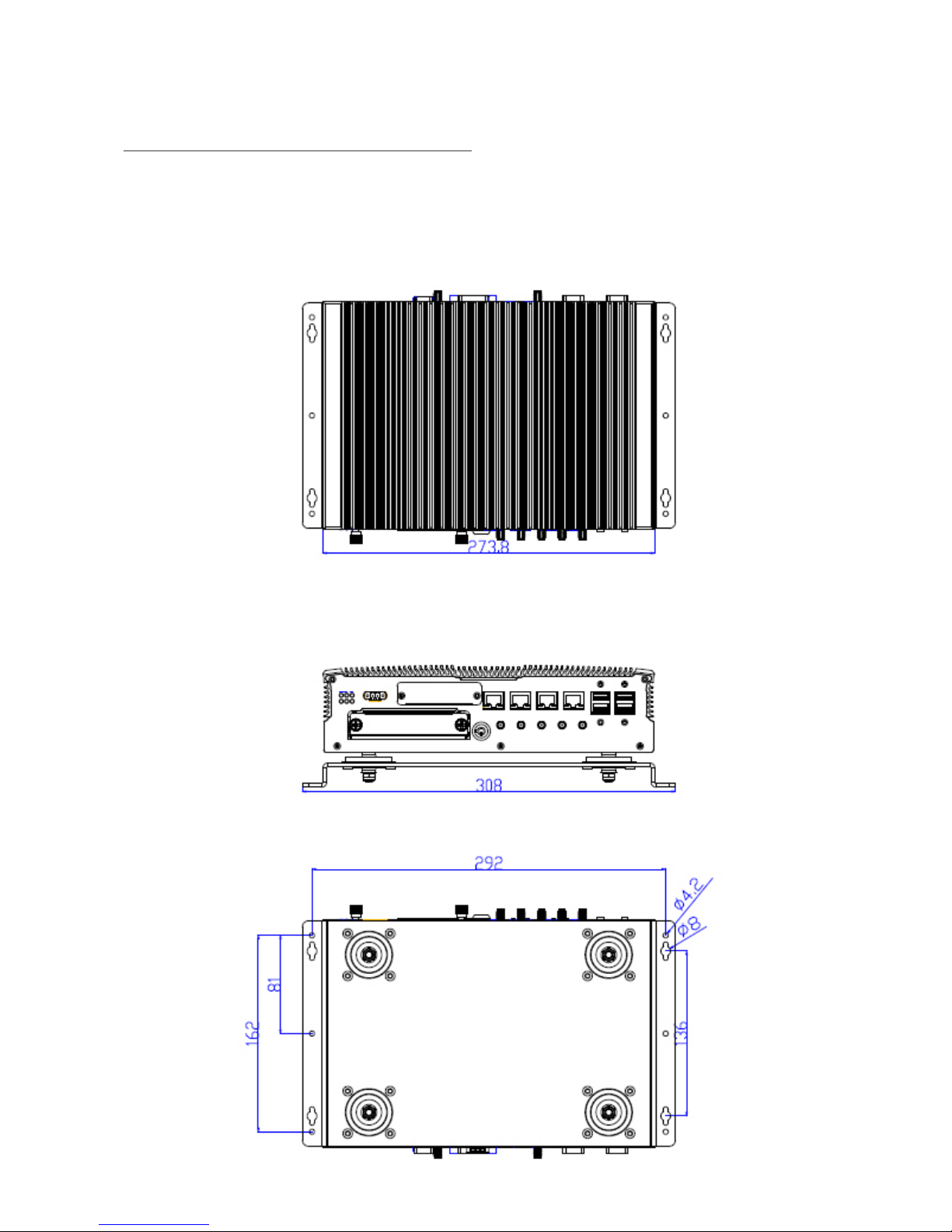
System Drawing
Mechanical dimensions of the LVC-5000-B series
Unit: mm
Page 8
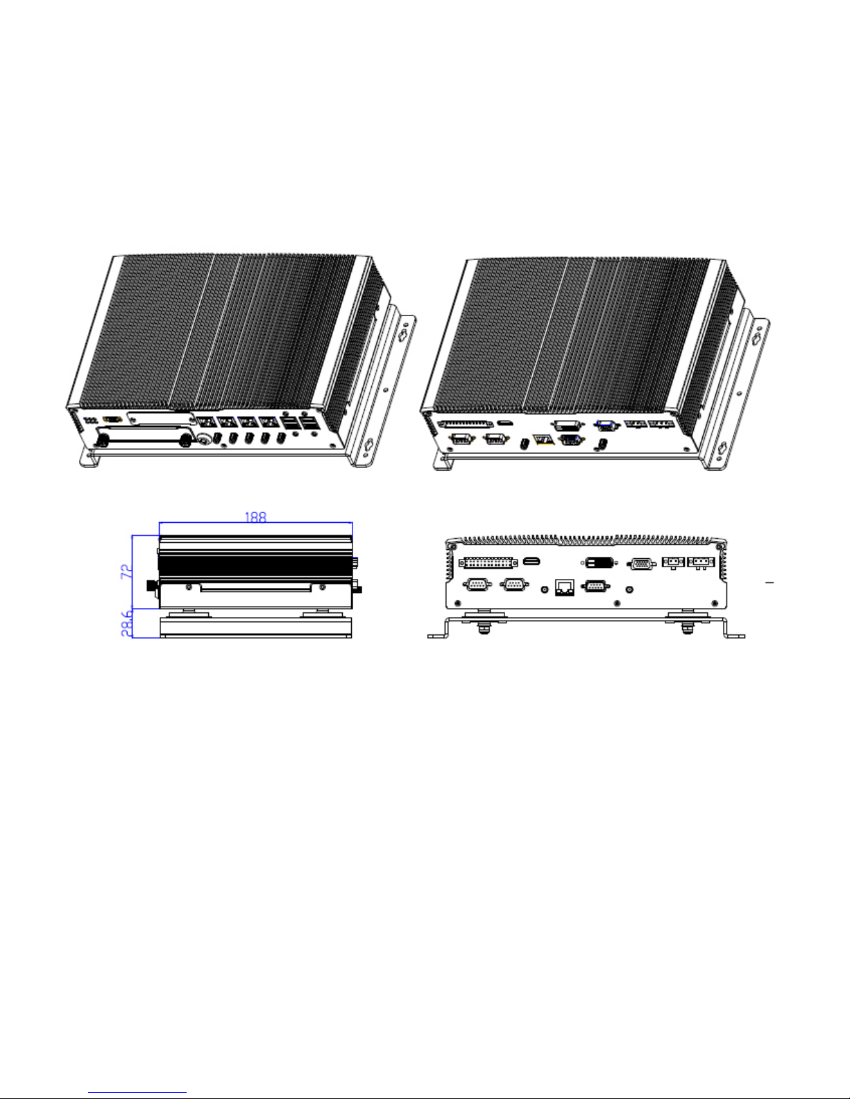
Notes: This mechanical drawing set is for reference only. Dimensions for all models B0, B1, B2 and B3 are the same
but I/O connectors may vary due to planning purposes.
Page 9
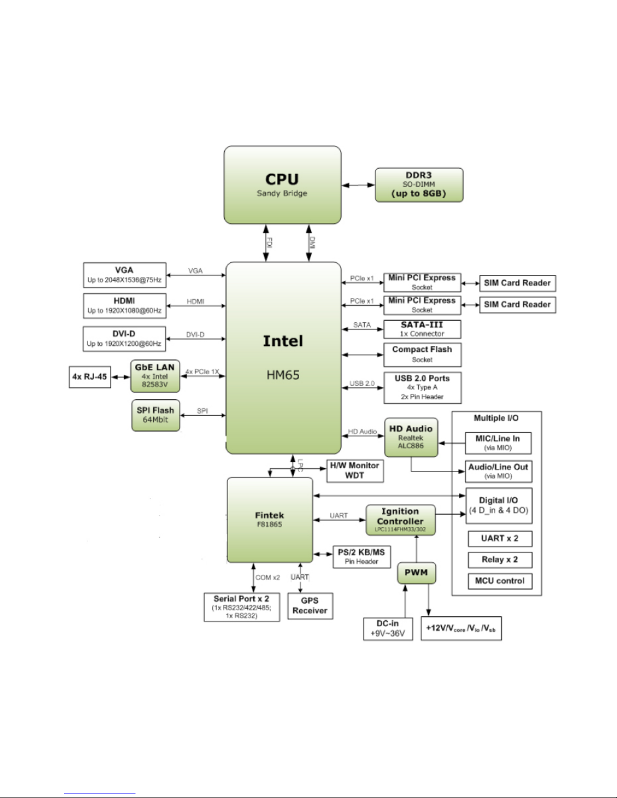
Block Diagram: The MainBoard
LVC-5000-B series comes with various CPU and I/O
options. Thus, there are more than one block diagrams to
be presented in the following.
LVC-5000-B0 block diagram:
Page 10
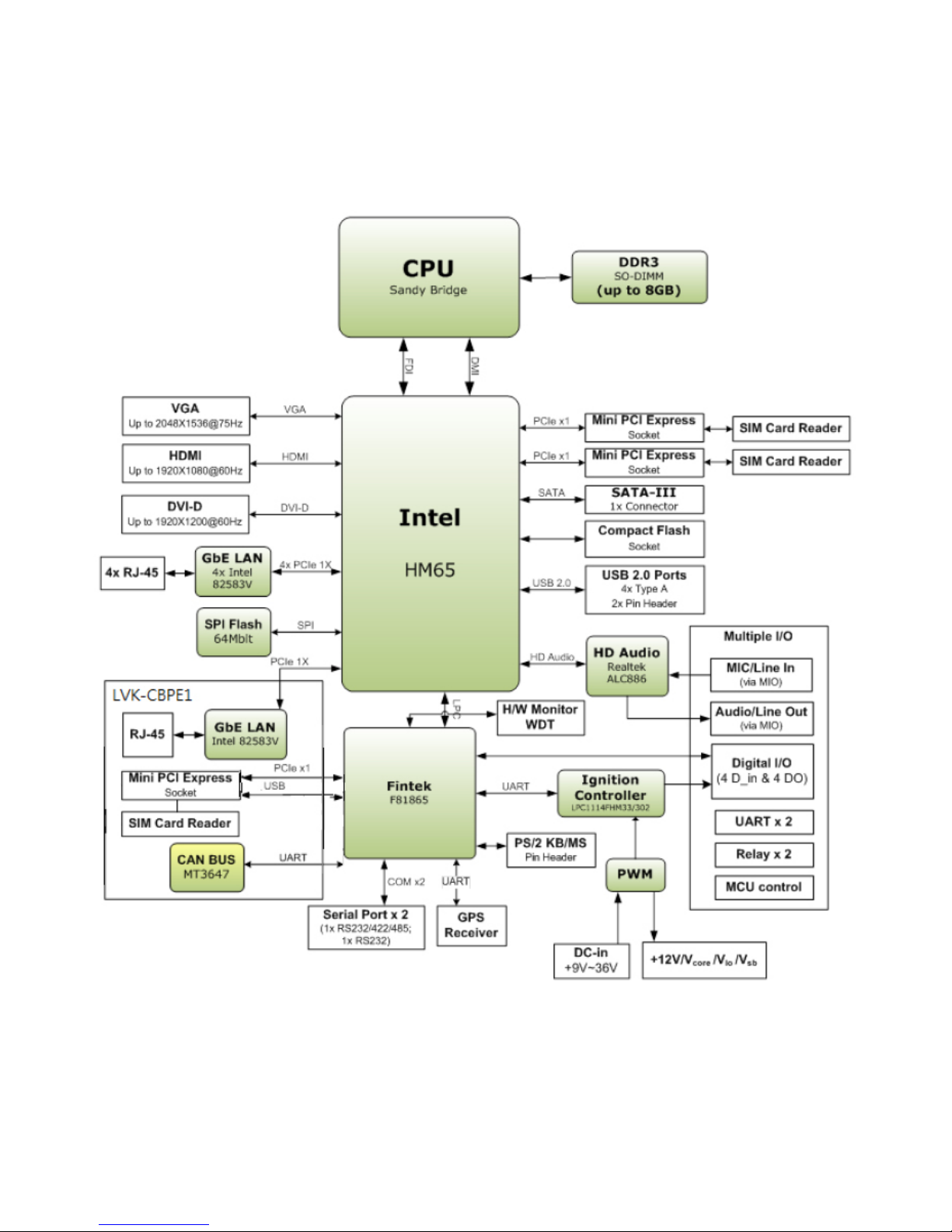
LVC-5000-B1/B2 block diagram:
Page 11
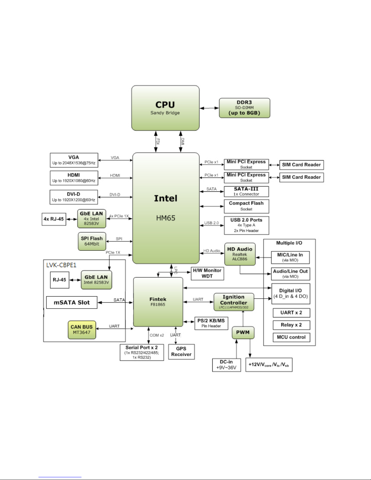
LVC-5000-B3 block diagram:
Page 12
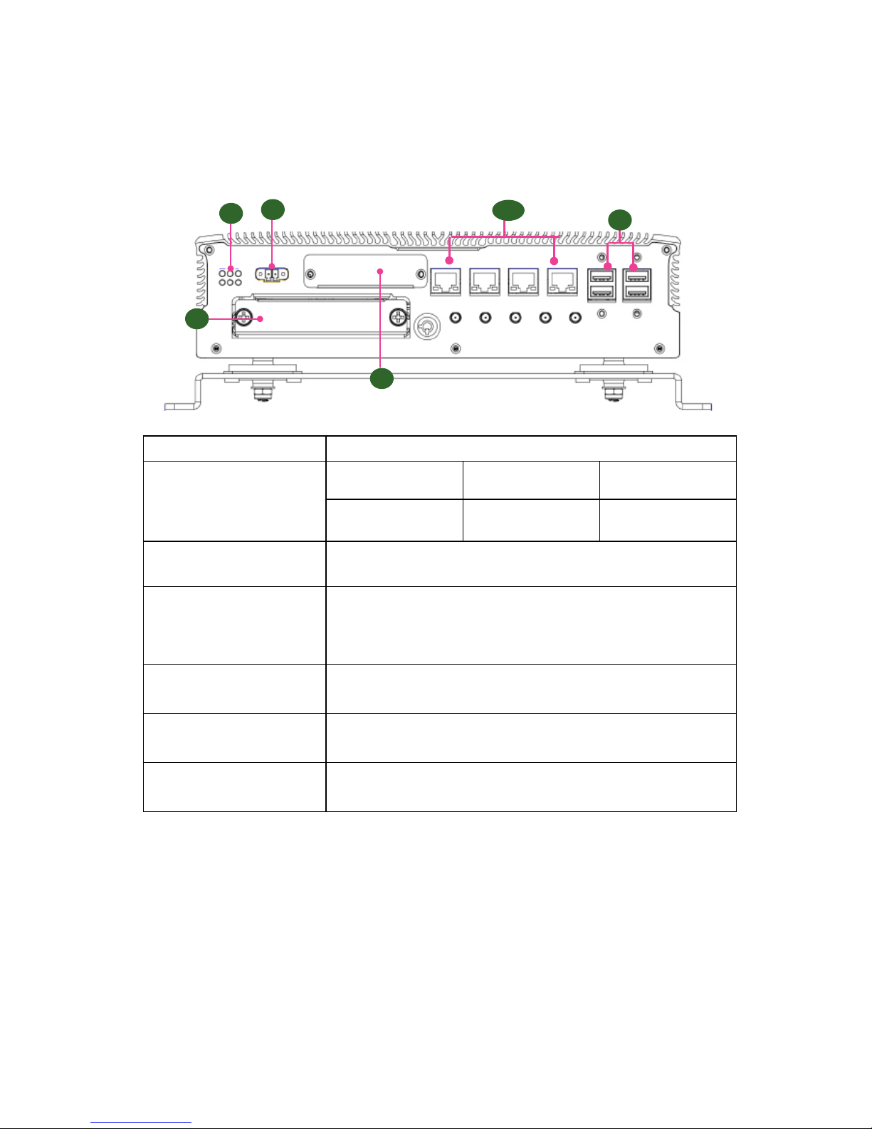
Front Components
F1
F5
F2
F3
F4
Component Description
F1 LED Indicators x 6 for
component status
HDD status 3G status PoE stats
Power WiFi status Ignition status
F2 Remote Power Switch 1x2-pin terminal block for distant power-on/off control
F3 Four 10/100/1000Mbps LAN
ports
Four RJ-45 (provided by Intel 82583V) jacks with LED indicators
They are provided by Intel 82583V GbE chips with Power over Ethernet
power source capability (48V, 15.4W).
F4 Four USB 2.0 Ports USB type A connectors
F5 2.5” Storage Drive Bay with
Lock (†)
Removable 2.5” storage drive for easy replacement of the storage
F6 CF/SIM card Slot (Sealed by
nails)
Externally accessible CF/SIM card slot sealed by nails
F6
All LVC-5000-B series models share common I/O components at the front panel.
Page 13

Rear Components
Component Description
R1 Multiple-I/O Connector A 26-pin male connector configured as followed:
4x DI ( 5V or 12V TTL selectable)•
4x DO (12V TTL , Max. 100mA)•
2x DO control Relay support 9~36V@max 2A each •
2x DI to Ignition MCU as remote control ( 5V TTL)•
Audio MIC input and HD Audio output (w/2Watt)•
COM TX RX, for Ignition Microcontroller program/•
service purpose.
R2 HDMI HDMI video/audio output port enabled by Intel
HD graphics
R3 DVI-D DVI-D port (single link) enabled by Intel HD
Graphic Engine.
R4 VGA VGA display port
R5 DC Output 12V 1x 2-pin terminal block for DC 12V (1A)Output
R6 DC Input 9-36V 3-pin power input range +9~+36V, GND, ignition
R7 Serial Ports (from left to
right: COM3/COM4)
COM3 - RS232
COM4 - RS232/422/485
R1
R2
R3
R4
R5 R6
R7
All LVC-5000-B series models show variations in terms of rear panel I/O components.
LVC-5000-B0
Page 14
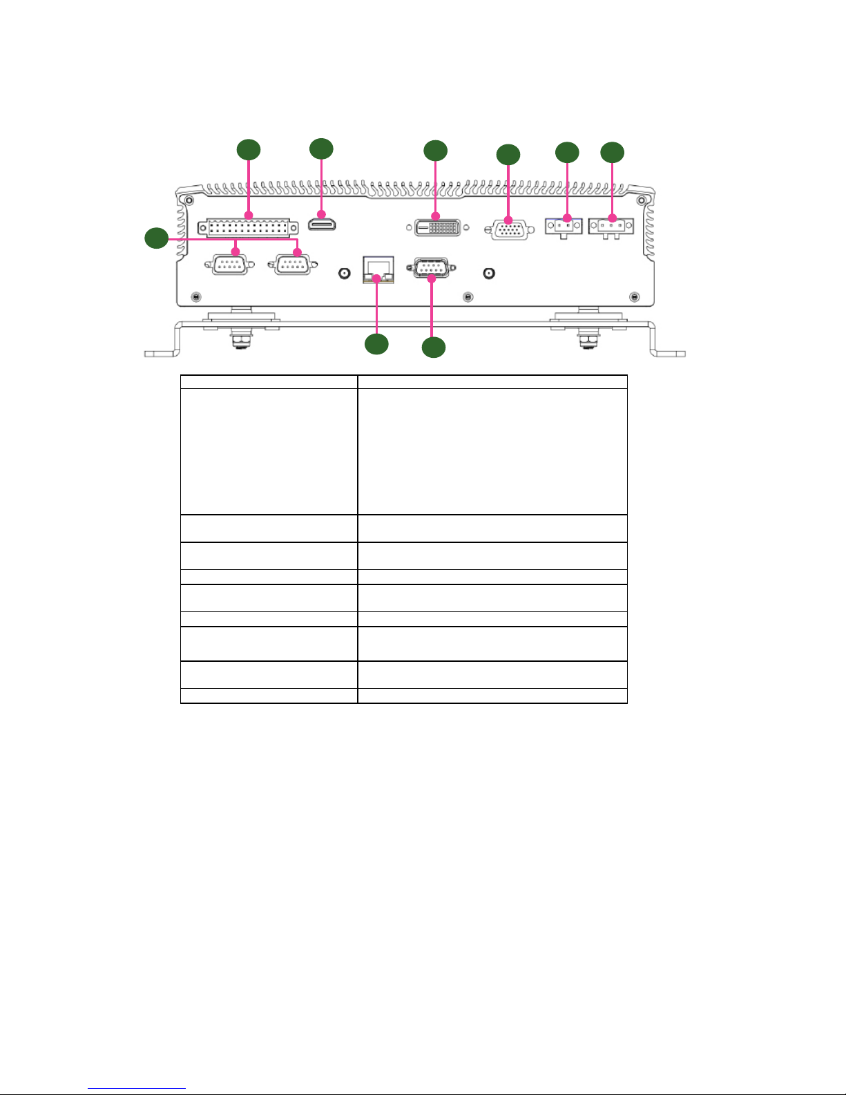
Component Description
R1 Multiple-I/O Connector A 26-pin male connector configured as followed:
4x DI ( 5V or 12V TTL selectable)•
4x DO (12V TTL , Max. 100mA)•
2x DO control Relay support 9~36V@max 2A each •
2x DI to Ignition MCU as remote control ( 5V TTL)•
Audio MIC input and HD Audio output (w/2Watt)•
COM TX RX, for Ignition Microcontroller program/•
service purpose.
R2 HDMI HDMI video/audio output port enabled by Intel
HD graphics
R3 DVI-D DVI-D port (single link) enabled by Intel HD
Graphic Engine.
R4 VGA VGA display port
R5 DC Output 12V 1x 2-pin terminal block for DC 12V (1A)Output
R6 DC Input 9-36V 3-pin power input range +9~+36V, GND, ignition
R7 Serial Ports (from left to
right: COM3/COM4)
COM3 - RS232
COM4 - RS232/422/485
R8 LAN One additional RJ-45 LAN port for B1, B2 and B3
models
R9 CAN CAN bus port for B1, B2 and B3 models
R1
R2
R3
R4
R5 R6
R7
LVC-5000-B1/B2/B3
R8
R9
Page 15
Chapter 3:
Motherboard Information
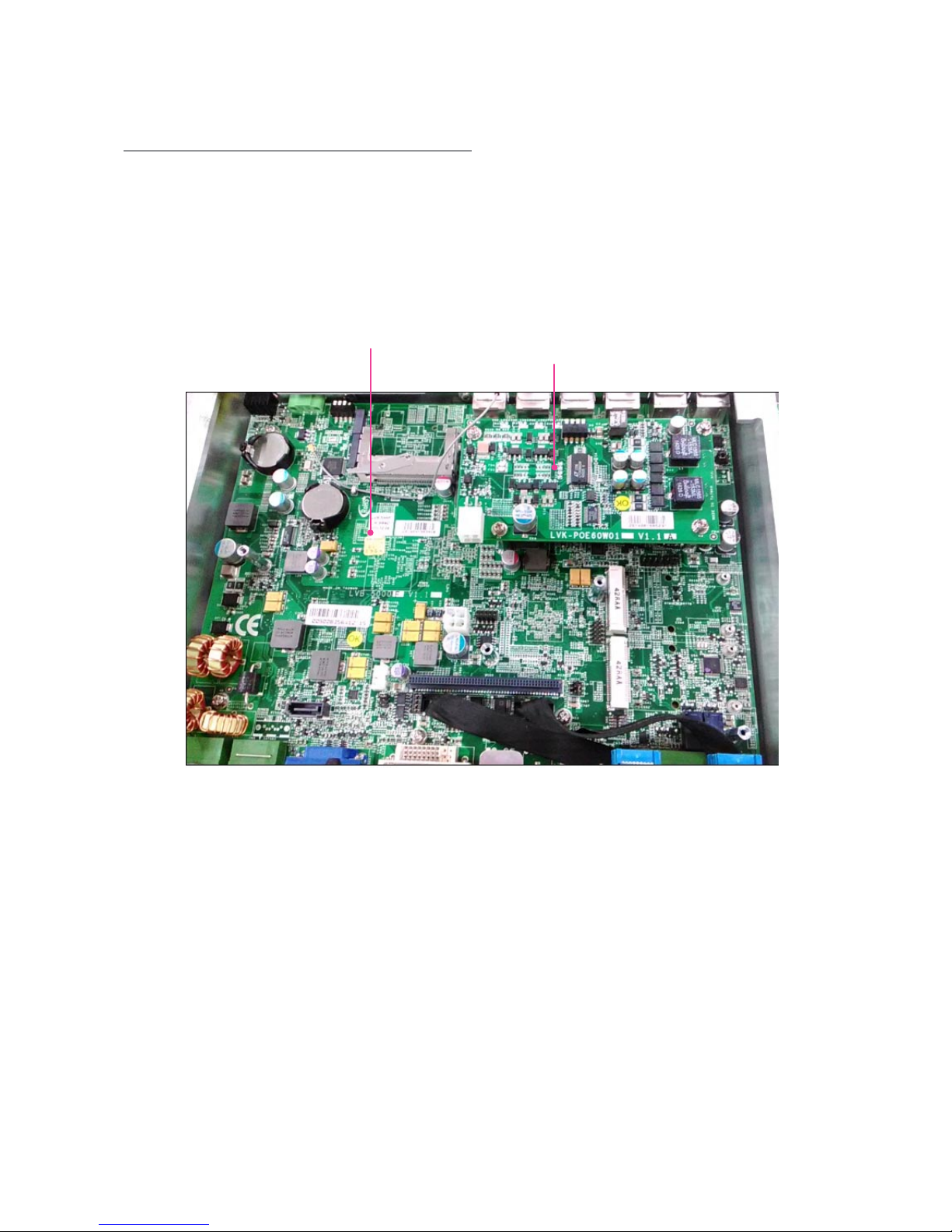
Inside LVC-5000-B Series
Though all models of LVC-5000-B series share the
same main motherboard, they come in card/board
combinations due to slight differences in specifications.
Please see the following for references.
PoE Power Board:
LVK-POE60W01
The main motherboard
LVC-5000-B0 At A Glance
Page 16
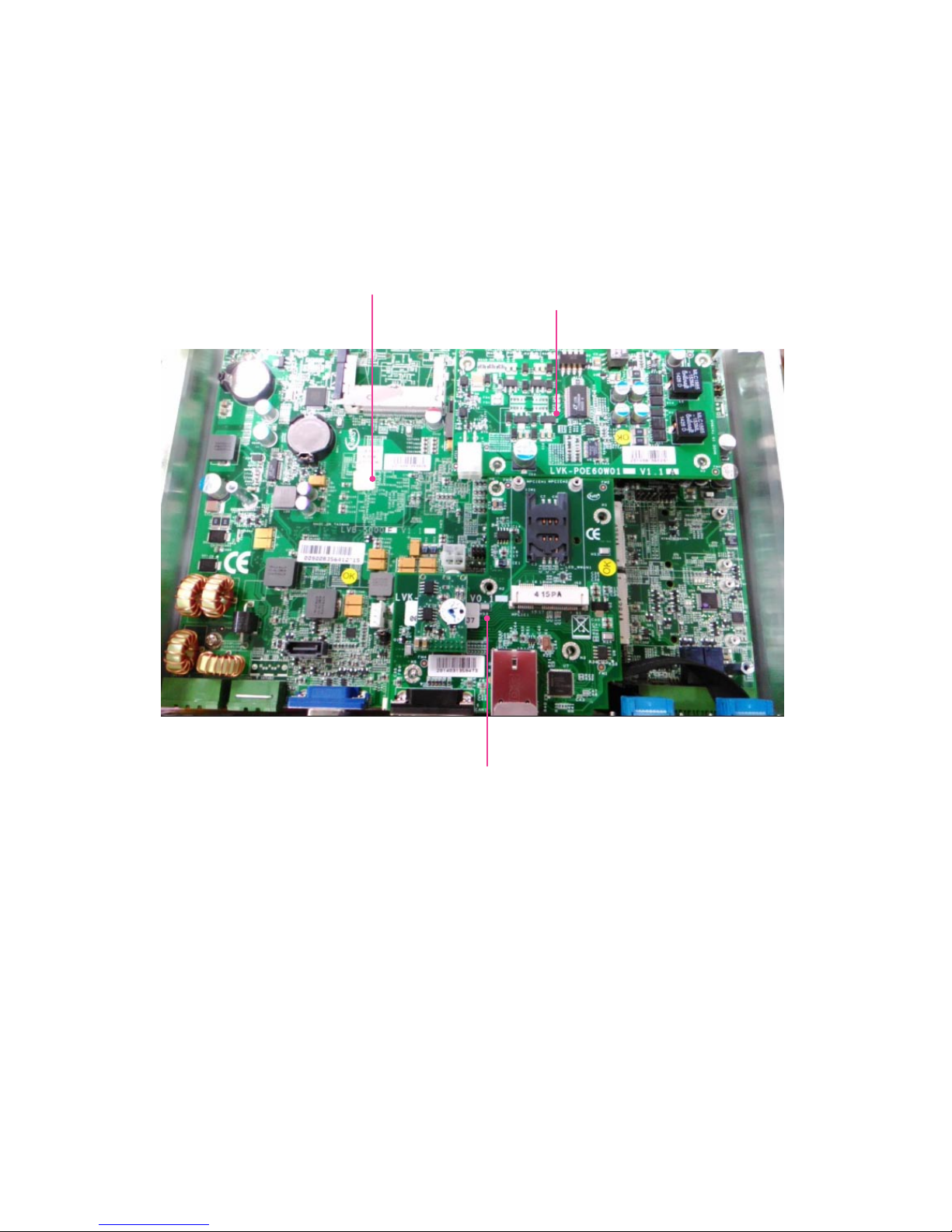
LVC-5000-B1/B2 At A Glance
PoE Power Board:
LVK-POE60W01
The main motherboard
Add-on card:
LVK-CBPE1
Page 17
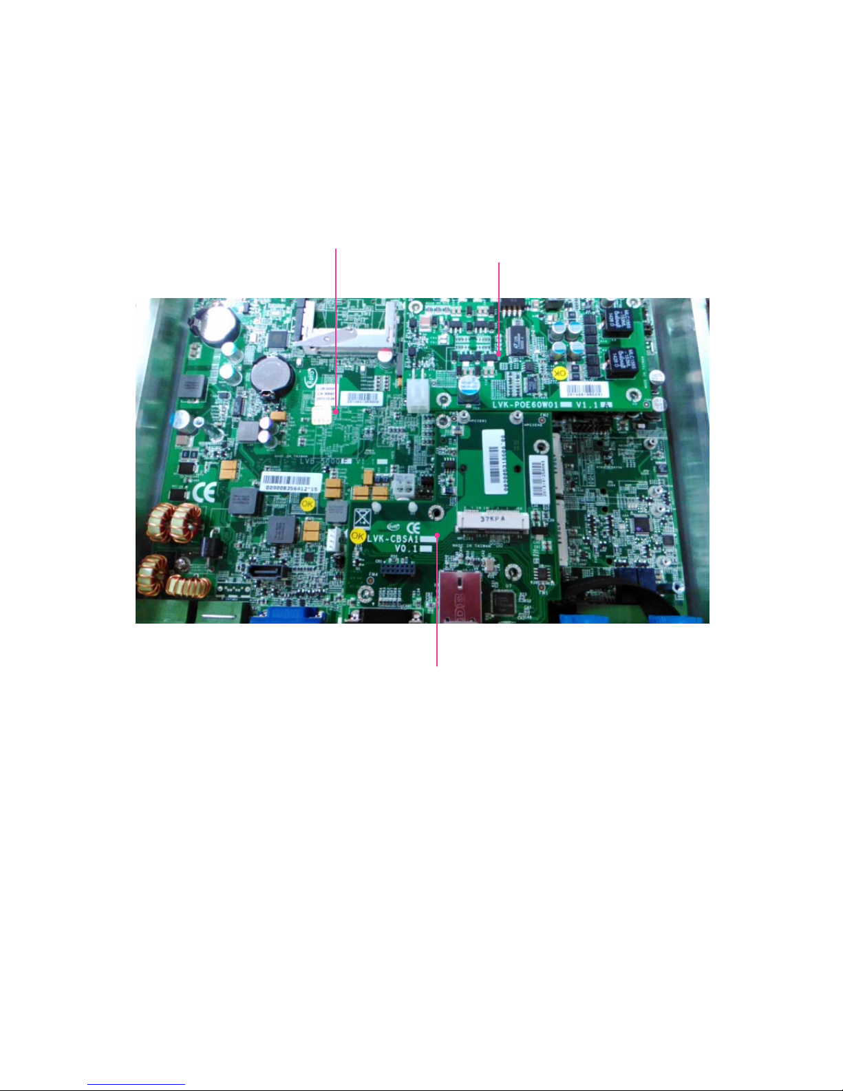
LVC-5000-B3 At A Glance
PoE Power Board:
LVK-POE60W01
The main motherboard
Add-on card:
LVK-CBSA1
Page 18
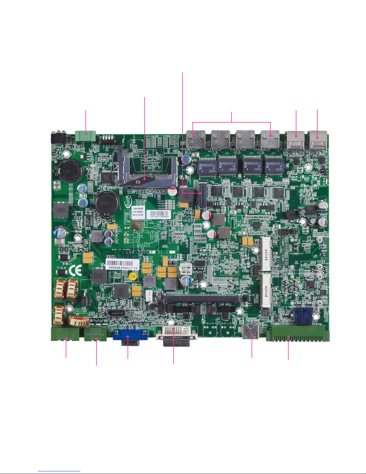
Jumpers & Connectors on the Motherboard
LAN1/LAN2/LAN3/LAN4 USBB1
USBB2
CN3
CN5
PRJK1
DVID1
VGAA1
MIO2
HDMI1
CF1
POEIO1
Page 19
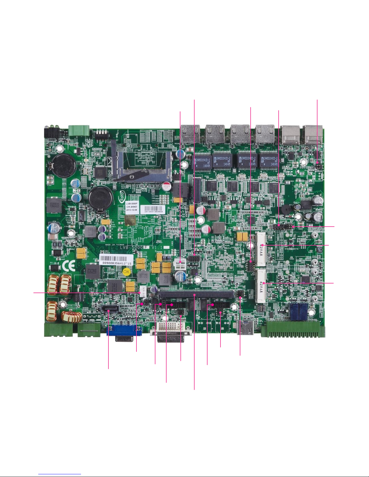
MPCIE1
MPCIE2
AUDIOIN1
COMSLT1
LPC1
CMOS1
PKMB1
SPI1
PS4M1
PCOM2
COMB2
COMB1
PCOM1
MIO3
SCT1
SCT2
PS4S1
SATAB1
Page 20
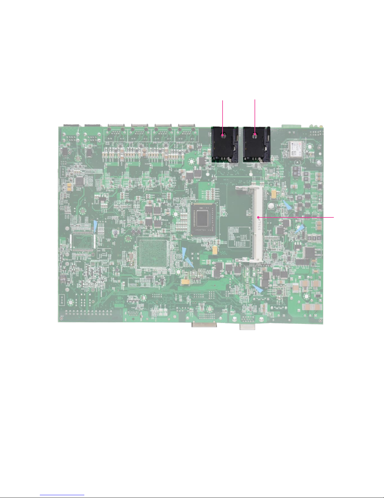
SIM2
SIM1
Jumpers & Connectors on the Motherboard
(Bottom side)
DIMM
Page 21
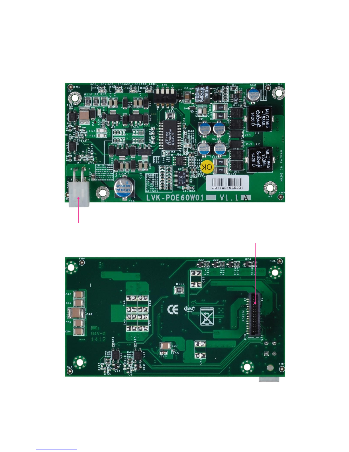
Jumpers & Connectors on the PoE Power Board
ATX1
POEIO1
Top Side
Bottom Side
Page 22
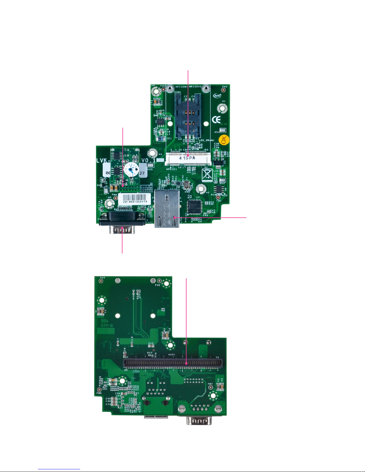
Jumpers & Connectors on the Add-on Card LVK-CBPE1
MPCIE1
CN1 (module
optional)
LAN1
CAN1
MIO1 (to connect with MIO3 on the
main motherboard)
Page 23
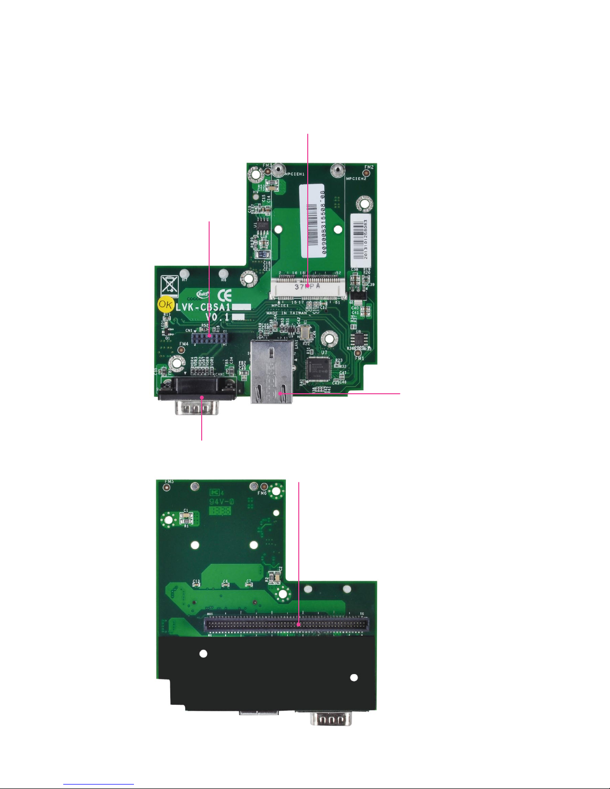
Jumpers & Connectors on the Add-on Card LVK-CBSA1
MPCIE1
CN1
LAN1
CAN1
MIO (to connect with MIO3 on the main
motherboard)
Page 24

Connectors and Jumpers List
Table 3.1 Connector List for LVK-POE60W01 Board
Labels Function
ATX1 ATX Power Connector
POEIO1 Connector for connecting to the mainboard
SW1 PoE setting
Table 3.2 Connector List for LEB-5000 Board
Labels Function
AUDIOIN1 Line-in/Mic-in Connector
CMOS1 Cleaning CMOS Data Including RTC
CF1 CF Card Slot
CN2 RS-232 Connector for MCU Programming
CN3 Distant Power on/off Control Connector
CN5
12VDC Power Output
COMB1/COMB2 RS232/422/485 internal pin headers
COM3/COM4 RS232/422/485 serial ports
DVID1 DVI-D Connector
SPI1 Serial Peripheral Interface Bus
HDMI1 HDMI Port
LANB1/LANB2/LANB3/
LANB4
Ethernet Connector 1~4
LPC1 Low Pin Count Interface
MIO2 26-pin multiple I/O external connector
MIO3 Connector between the main board and add-on card or PoE Power
board via PCI Express
MPCIE1/MPCIE2 Mini-PCIe Connector 1 & 2
PCOM1/PCOM2 Select COM1/COM2 Pin9 Function
PKMB1 PS/2 Keyboard and Mouse Connector
PRJK1 DC-in with Ignition Control
POEIO1 POE board LVK-POE60W01 connectors
PS4M1 Connector for connecting ATX1 on LVK-POE60W01
PS4S1 SATA Power
SATAB1 Serial-ATA Connector
SCT1/SCT2 Select COM2 Protocol Setting
SIM1/SIM2 SIM Card Readers
SW1/SW2 Power Control Function Selection
USBB1/USBB2 USB Type A Connector #0,1; #2,3
VGAA1 VGA Port
COMSLT1 GPIO setting
Table 3.3 Connector List for LVK-CBPE1 Board
Labels Function
MIO1 Connector between the main board and add-on card or PoE Power
board via PCI Express
CAN1 CAN bus port
LAN1 LAN port
CN1 Interpreter module connector
MPCIE1 Mini PCIe socket with SIM card reader
Table 3.4 Connector List for LVK-CBSA1 Board
Labels Function
MIO1 Connector between the main board and add-on card or PoE Power
board via PCI Express
CAN1 CAN bus port
LAN1 LAN port
CN1 Interpreter module connector
MPCIE1 mSATA slot
Page 25
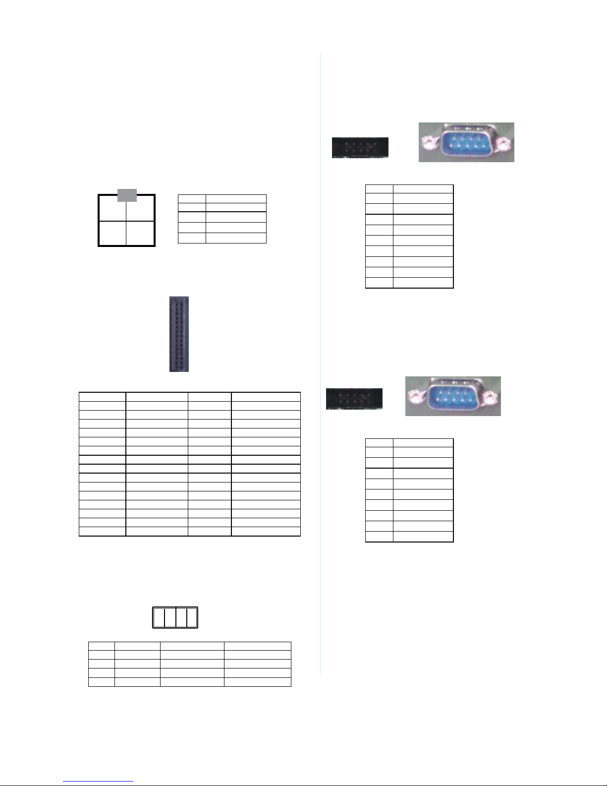
COM3 RS-232 Serial Port (COMB1): RS-232 DB9 COM
port connected to and enabled by an internal COM
connector
COM2 RS-232/422/485 Serial Port (COMB2): An
RS-232/422/485 port through the D-SUB9 connector,
connected with and enabled by an internal COM
connector.
Jumper Settings & Connector Pinouts
ATX1: ATX Power connector which connects to PS4M1
on the mainboard.
POEIO1: Connector for connecting to the mainboard
Pin No. Description Pin No. Description
A1 VPORT_OUT3 B1 VPORT_OUT2
A2 VPORT_OUT3 B2 VPORT_OUT2
A3 VPORT_OUT3 B3 VPORT_OUT2
A4 N/A B4 N/A
A5 VPORT_OUT4 B5 VPORT_OUT1
A6 VPORT_OUT4 B6 VPORT_OUT1
A7 VPORT_OUT4 B7 VPORT_OUT1
A8 N/A B8 N/A
A9 GPIO_SD4 B9 AGND1_4266
A10 GPIO_SD3 B10 AGND1_4266
A11 GPIO_SD2 B11 AGND1_4266
A12 GPIO_SD1 B12 AGND1_4266
A13 VCC5_PS B13 AGND1_4266
A14 N/A B14 AGND1_4266
A15 AGND1_4266 B15 AGND1_4266
SW1
LVB-5000 Board
Pin No. Description
1 SP3_DCD
2 SP3_DSR
3 SP3_RXD
4 SP3_RTS
5 SP3_TXD
6 SP3_CTS
7 SP3_DTR
8 VCC_RI4
9 GND
LVK-POE60W01
Pin No. Pin Name
1 GND
2 DC_VIN (9-36V)
3 GND
4 DC_VIN (9-36V
4 2
3 1
Pin No. Description
1 SP3_DCD
2 SP3_DSR
3 SP3_RXD
4 SP3_RTS
5 SP3_TXD
6 SP3_CTS
7 SP3_DTR
8 VCC_RI3
9 GND
1 2 3 4
SW1
Pin No. PoE port PSE Power Enable PSE Power Disable
1 Port1 Off On
2 Port2 Off On
3 Port3 Off On
4 Port4 Off On
Page 26
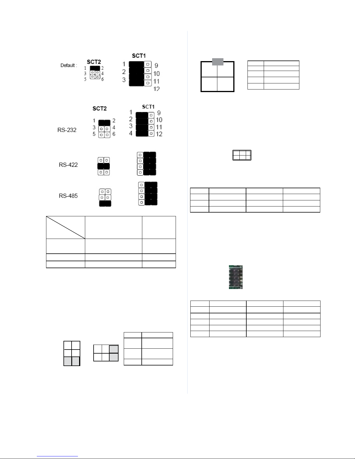
SCT1, SCT2: Select COMB2 Protocol Setting
Switch
Protocol
SCT1 SCT2
RS-232
(default)
1-5, 2-6, 3-7, 4-8 1-2
RS-422 5-9, 6-10, 7-11, 8-12 3-4
RS-485 5-9, 6-10, 7-11, 8-12 5-6
PCOM1, PCOM2: configure COM1 and COM2 Pin9
Function (in RS-232) respectively. The Ring indicator
pinout of the RS-232 COM port can be altered according
to the following jumper settings.
PS4M1: Connect to the ATX1 power connector on the
LVK-POE60W01 board
AUDIOIN1: Line-in and Mic-in Connector
LPC1: Low Pin Count Connector
Pin No. Pin Name
1 GND
2 DCIN_VCC
3 GND
4 DCIN_VCC
2 1
4 3
Pin No. Pin No. Pin Name
1 MIC_in_R 2 MIC_in_L
3 Audio_in_R 4 Audio_in_L
5 Line_in1_R 6 Line_in1_L
1 3 5
2 4 6
Pin No. Function
1-2 Supply +5V to
the Device
3-4 Supply +12V to
the Device
5-6 Ring-in (default)
2 4 6
PCOM1
2
4
6
1
3
5
1 3 5
PCOM2
Pin No. Signal Pin No. Signal
1 33MHz CLK 2 LAD1
3 RESET 4 LAD0
5 FRAME 6 VCC3.3
7 LAD3 8 GND
9 LAD2 10 GND
Page 27
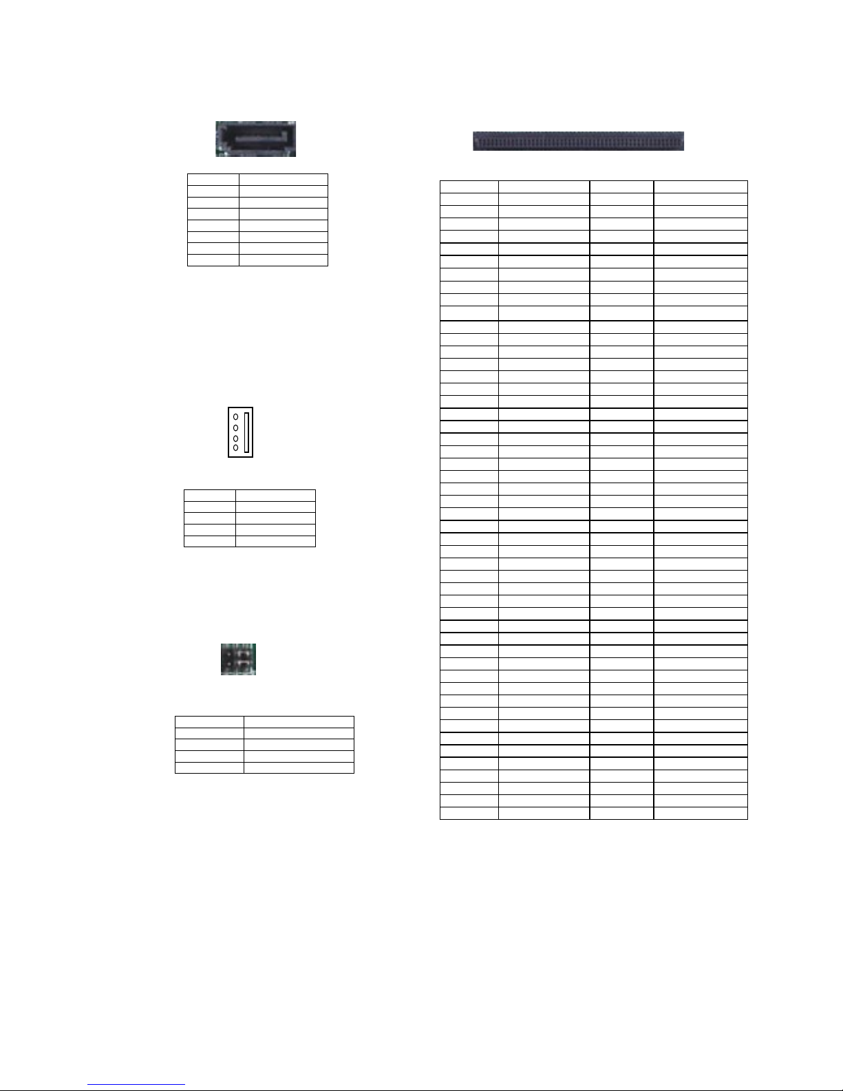
MIO3: 2x50 Dual-Row Socket for any extension board
on the mainboard:
PIN Pin Name PIN Pin Name
1 GND 51 HDA_BCLK_PCH
2 PCH_SATATXN3 52 HDA_SYNC_PCH
3 PCH_SATATXP3 53 HDA_RST_N_PCH
4 GND 54 HDA_SDIN1_PCH
5 PCH_SATARXN3 55 HDA_SDO_PCH
6 PCH_SATARXP3 56 SPK_PCH
7 GND 57 VCC3P3_SB
8 VCC3P3_PS 58 VCC3P3_SB
9 VCC3P3_PS 59 VCC3P3_SB
10 VCC3P3_PS 60 VCC3P3_SB
11 GND 61 VCC3P3_SB
12 PCH_PCIE_RXN8 62 PCH_PCIE_RXN2
13 PCH_PCIE_RXP8 63 PCH_PCIE_RXP2
14 PCH_PCIE_TXN8 64 PCH_PCIE_TXN2
15 PCH_PCIE_TXP8 65 PCH_PCIE_TXP2
16 PCIE_CKN8 66 PCIE_CKN2
17 PCIE_CKP8 67 PCIE_CKP2
18 N/A 68 N/A
19 PLTRST_BUF1_N 69 SMBCLK_RESUME
20 WAKE_N 70 SMBDAT_RESUME
21 DCIN_VCC 71 N/A
22 VCC12 72 N/A
23 VCC5_SB 73 PCH_USB_N12
24 VCC5_SB 74 PCH_USB_P12
25 VCC5 75 GND
26 VCC5 76 USB_N13
27 VCC5 77 USB_P13
28 GND 78 GND
29 N/A 79 N/A
30 N/A 80 N/A
31 N/A 81 N/A
32 N/A 82 N/A
33 GND 83 GND
34 N/A 84 COM1_DCD#
35 N/A 85 COM1_RI#
36 N/A 86 COM1_CTS#
37 N/A 87 COM1_DTR#
38 N/A 88 COM1_RTS#
39 N/A 89 COM1_DSR#
40 N/A 90 COM1_SOUT
41 N/A 91 COM1_SIN
42 GND 92 GND
43 N/A 93 COM2_DCD#
44 N/A 94 COM2_RI#
45 N/A 95 COM2_CTS#
46 N/A 96 COM2_DTR#
47 N/A 97 COM2_RTS#
48 N/A 98 COM2_DSR#
49 N/A 99 COM2_SOUT
50 N/A 100 COM2_SIN
SATAB1 (SATA0): SATA7-pin signal connector for a
2.5” disk drive
4-pin Serial-ATA Power Connector (PS4S1): It is for
connecting the SATA power cord.
COMSLT11
Pin No. Description
1 VCC12
2 GND
3 GND
4 VCC5_PS
Pin No. Description
1 GND
2 PCH_SATATXP0
3 PCH_SATATXN0
4 GND
5 PCH_SATARXN0
6 PCH_SATARXP0
7 GND
4
3
2
1
Pin No. Description
Short 1-3 GPIO10 Enable
Short 3-5 GPIO10 Disable
Short 2-4 GPIO11 Enable
Short 4-6 GPIO11 Disable
Page 28
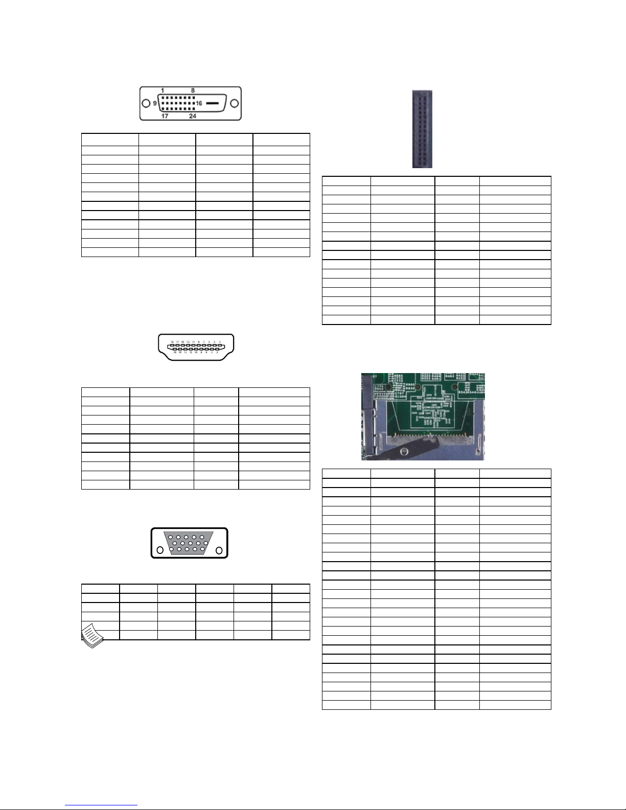
DVI-D Connector (DVID1): A single link DVI-D Connector
Pin No. Description Pin No. Description
1 PCH_DDPC_0N 2 PCH_DDPC_0P
3 GND 4 N/A
5 N/A 6 DVI_SCL
7 DVI_SDA 8 N/A
9 PCH_DDPC_1N 10 PCH_DDPC_1P
11 GND 12 N/A
13 N/A 14 VCC5_PS
15 GND 16 DVI_HPD
17 PCH_DDPC_2N 18 PCH_DDPC_2P
19 GND 20 N/A
21 N/A 22 GND
23 PCH_DDPC_3P 24 PCH_DDPC_3N
HDMI Connector (HDMI1): An HDMI Con-
nector
Pin No. Description Pin No. Description
1 HDMI_DATP2_P 2 GND
3 HDMI_DATP2_N 4 HDMI_DATP1_P
5 GND 6 HDMI_DATP1_N
7 HDMI_DATP0_P 8 GND
9 HDMI_DATP0_N 10 HDMI_CLK_P
11 GND 12 HDMI_CLK_N
13 N/A 14 N/A
15 HDMI_DDC_CLK 16 HDMI_DDC_DAT
17 GND 18 PHDMI
19 HDMI_HPD
VGA (VGAA1)
Pin Signal Pin Signal Pin Signal
1 RED 6 GND 11 N/A
2 GREEN 7 GND 12 DDC DAT
3 BLUE 8 GND 13 HSYNC
4 N/A 9 +5V_CRT 14 VSYNC
5 CRT_ON 10 GND 15 DDC CLK
Note: The driver for the VGA and Audio
ports should be installed with the following
order: Chipset INF->Graphic->Audio
15 14 13 12 11
5 4 3 2 1
POEIO1: Connector for Connecting to the POE
power board LVK-POE60W01
Pin No. Description Pin No. Description
A1 VPORT_OUT3 B1 VPORT_OUT2
A2 VPORT_OUT3 B2 VPORT_OUT2
A3 VPORT_OUT3 B3 VPORT_OUT2
A4 N/A B4 N/A
A5 VPORT_OUT4 B5 VPORT_OUT1
A6 VPORT_OUT4 B6 VPORT_OUT1
A7 VPORT_OUT4 B7 VPORT_OUT1
A8 N/A B8 N/A
A9 GPIO_SD4 B9 AGND1_4266
A10 GPIO_SD3 B10 AGND1_4266
A11 GPIO_SD2 B11 AGND1_4266
A12 GPIO_SD1 B12 AGND1_4266
A13 VCC5_PS B13 AGND1_4266
A14 N/A B14 AGND1_4266
A15 AGND1_4266 B15 AGND1_4266
CF1: CF Card Slot
Pin No. Description Pin No. Description
1 GND 26 CF_DIS_N
2 CF_DD3 27 CF_DD11
3 CF_DD4 28 CF_DD12
4 CF_DD5 29 CF_DD13
5 CF_DD6 30 CF_DD14
6 CF_DD7 31 CF_DD15
7 CF_DCS0 32 -CF_DCS1
8 GND 33 CF_VS1
9 GND 34 CF_DIOR_N
10 CF_SATA_RXP_R 35 CF_DIOW_N
11 CF_SATA_RXN_R 36 VCC3P3_PS
12 GND 37 CF_IDEIRQ
13 CF_PW 38 CF_PW
14 GND 39 MST_SLV
15 CF_SATA_TXN_R 40 CF_VS2
16 CF_SATA_TXP_R 41 CF_IDERST_N
17 GND 42 CF_IORDY
18 CF_DA2 43 CF_DMARQ
19 CF_DA1 44 CF_DDACK_N
20 CF_DA0 45 CFACT_N
21 CF_DD0 46 CF_PDIAG
22 CF_DD1 47 CF_DD8
23 CF_DD2 48 CF_DD9
24 N/A 49 CF_DD10
25 CF_DIS_N 50 GND
Page 29
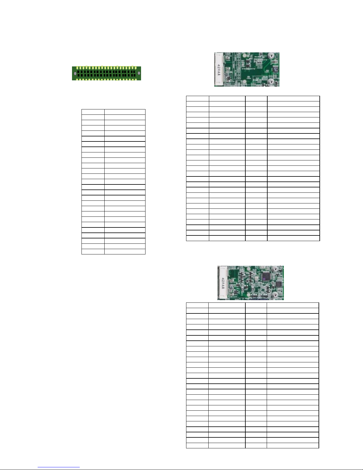
Multiple I/O Connectors (MIO2): 26-pin
external Multiple I/O for functions in Audio, serial
communication, Digital In/Out, Ignition detection input
for automatic wake-up function
Pin Signal
1 AUDIO_OUT_R
2 AUDIO_OUT_L
3 GND_AUD
4 GND_AUD
5 AMPOUT_R
6 AMPOUT_L
7 GND
8 N/A
9 COM5_SIN
10 COM5_SOUT
11 DI_0
12 DO_0
13 DI_1
14 DO_1
15 DI_2
16 DO_2
17 DI_3
18 DO_3
19 IGN_DI0
20 RELAY1_NOPEN
21 IGN_DI1
22 RELAY1_COMM
23 GND
24 GND
25 RELAY2_NOPEN
26 RELAY2_COMM
25 1
26 2
MPCIE1: Mini-PCIe Connector with one SIM Card
Reader(SIM1). It supports both Wi-Fi and 3G module.
Pin Signal Pin Signal
1 PCIE_WAKE_N 2 VCC3P3_PS
3 N/A 4 GND
5 N/A 6 V1P5_MPCIE
7 E_CLKREQ- 8 UIM_PWR
9 GND 10 UIM_DAT
11 PCIE_CKN3 12 UIM_CLK
13 PCIE_CKP3 14 UIM_RESET
15 GND 16 UIM_VPP
17 RSV 18 GND
19 RSV 20 N/A
21 GND 22 BUF_PLT_RST#
23 PCH_PCIE_RXN3 24 PCIE_PCIE_VCC3AUX
25 PCH_PCIE_RXP3 26 GND
27 GND 28 V1P5_MPCIE
29 GND 30 SMBCLK_RESUME
31 PCH_PCIE_TXN3 32 SMBDATA_RESUME
33 PCH_PCIE_TXP3 34 GND
35 GND 36 PCH_USB_N8
37 GND 38 PCH_USB_P8
39 VCC3P3_PS 40 GND
41 VCC3P3_PS 42 LED_WWAN143 GND 44 LED_WLAN145 RSV 46 N/A
47 RSV 48 V1P5_MPCIE
49 RSV 50 GND
51 RSV 52 VCC3P3_PS
MPCIE2: Mini-PCIe Connector with one SIM Card
Reader(SIM2). It supports both Wi-Fi and 3G module.
Pin Signal Pin Signal
1 PCIE_WAKE_N 2 VCC3P3_PS
3 N/A 4 GND
5 N/A 6 V1P5_MPCIE
7 E_CLKREQ- 8 UIM2_PWR
9 GND 10 UIM2_DAT
11 PCIE_CKN4 12 UIM2_CLK
13 PCIE_CKP4 14 UIM2_RESET
15 GND 16 UIM2_VPP
17 RSV 18 GND
19 RSV 20 N/A
21 GND 22 BUF_PLT_RST#
23 PCH_PCIE_RXN4 24 PCIE_PCIE_VCC3AUX
25 PCH_PCIE_RXP4 26 GND
27 GND 28 V1P5_MPCIE
29 GND 30 SMBCLK_RESUME
31 PCH_PCIE_TXN4 32 SMBDATA_RESUME
33 PCH_PCIE_TXP4 34 GND
35 GND 36 PCH_USB_N9
37 GND 38 PCH_USB_P9
39 VCC3P3_PS 40 GND
41 VCC3P3_PS 42 LED_WWAN243 GND 44 LED_WLAN245 RSV 46 N/A
47 RSV 48 V1P5_MPCIE
49 RSV 50 GND
51 RSV 52 VCC3P3_PS
Page 30
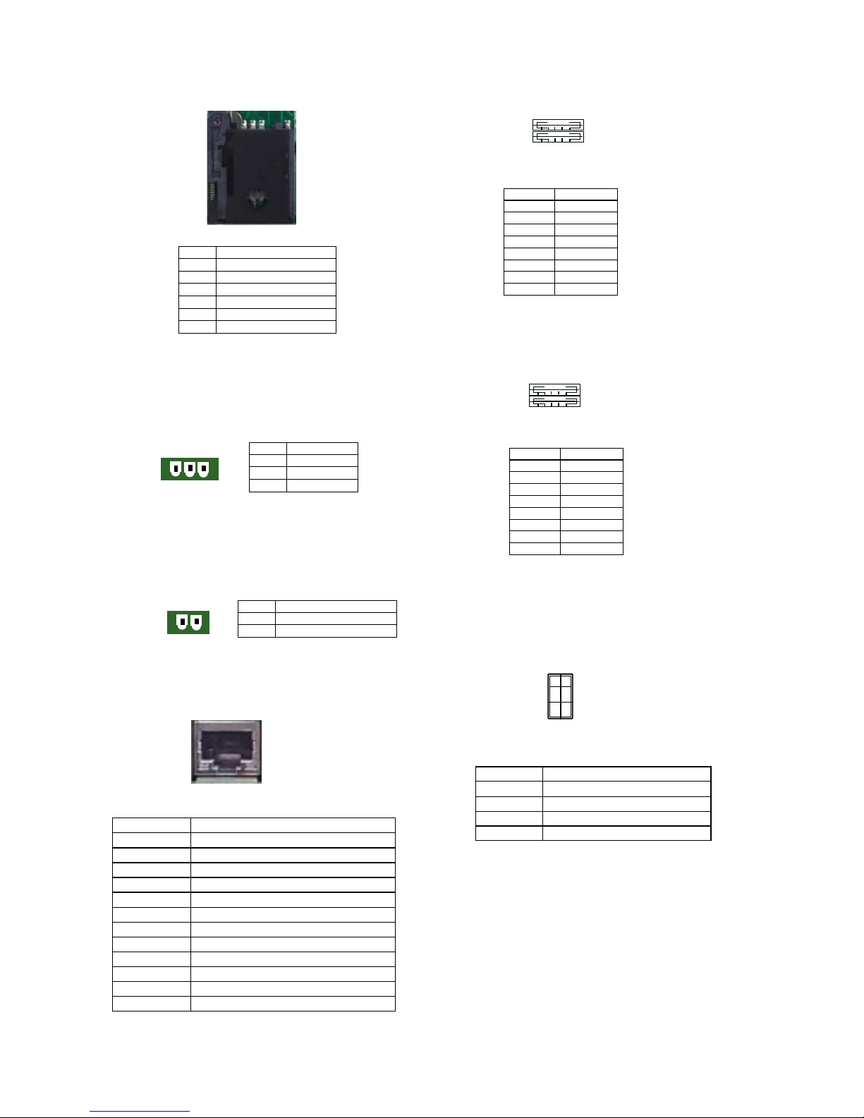
SIM Card Socket (SIM1/SIM2): SIM card slots
Power-in with Ignition Control (PRJK1): A power
connector with power -ignition Control
Distant Power on/off Control (CN3)
LAN1~4 Ports (LANB1~LANB4):
Pin No. Description
1 LAN_MDI0_P
2 LAN_MDI0_N
3 LAN_MDI1_P
4 LAN_MDI2_P
5 LAN_MDI2_N
6 LAN_MDI1_N
7 LAN_MDI3_P
8 LAN_MDI3_N
9 LAN_ACTLED_P
10 LAN_ACTLED_N
11 LAN_L1000_N
12 LAN_L100_N
Pin No. Pin Name
1 Ignition
2 GND
3 DC_IN
3 2 1
Pin No. Description
C1 UIM_PWR
C2 UIM_RST
C3 UIM_CLK
C5 GND
C6 UIM_VPP
C7 UIM_DAT
2 1
Pin No. Pin Name
1 Remote_Power_on
2 GND
Dual USB 2.0 Ports USB0 & USB1(USBB1)
Dual USB 2.0 Port s USB2 & USB3 (USBB2)
Clear CMOS:
1 2 3 4
5 6 7 8
Pin No. Pin Name
1 VCC5
2 USBD0N
3 USBD0P
4 GND
5 VCC5
6 USBD1N
7 USBD1P
8 GND
Pin No. Pin Name
Short 1-3 Normal (Default)
Short 3-5 Clear RTC
Short 2-4 Normal
Short 4-6 Clear CMOS
Pin No. Pin Name
1 VCC5
2 USBD2N
3 USBD2P
4 GND
5 VCC5
6 USBD3N
7 USBD3P
8 GND
6
4
2
5
3
1
1 2 3 4
5 6 7 8
Page 31
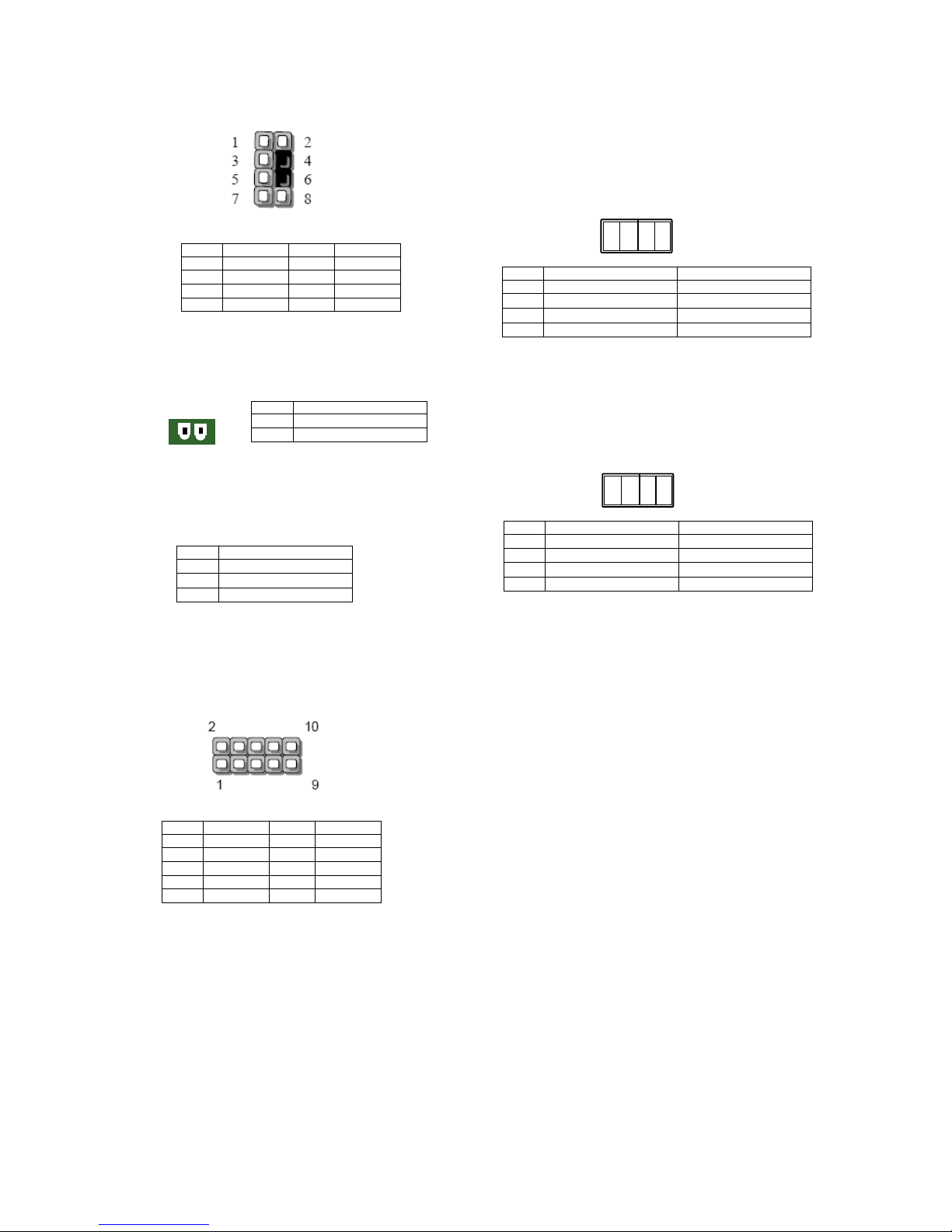
PS/2 Keyboard and Mouse Connector (PKMB1)
12VDC Power Output (CN5)
CN2:
SPI1:
Pin No. Signal Pin No. Signal
1 VCC5_KB 2 KCLK
3 MDAT
5 KDAT
7 GND 8 MCLK
2 1
Pin No. Pin Name
1 VCC12_PS
2 GND
Pin No. Pin Name
1 EXT_RXD
2 GND
3 EXT_TXD
SW1 & SW2: Function Select
Default Pin1 & Pin2 ON, Pin3 & Pin4 OFF
1 2 3 4
SW1
Pin No. Signal Pin No. Signal
1 SPI_HOLD 2 N/A
3 SPI_CS0 4 VCC3
5 SPI_MISO 6 N/A
7 N/A 8 SPI_CLK
9 GND 10 SPI_MOSI
Pin No. Setting Description
1 On/Off Detect Power Good
2 On/Off Low Power Detect
3 On/Off Watch dog
4 On/Off RSVD
1 2 3 4
SW2
Pin No. Setting Description
1 On/Off Normal
2 On/Off Normal
3 On/Off Program
4 On/Off Program
Page 32
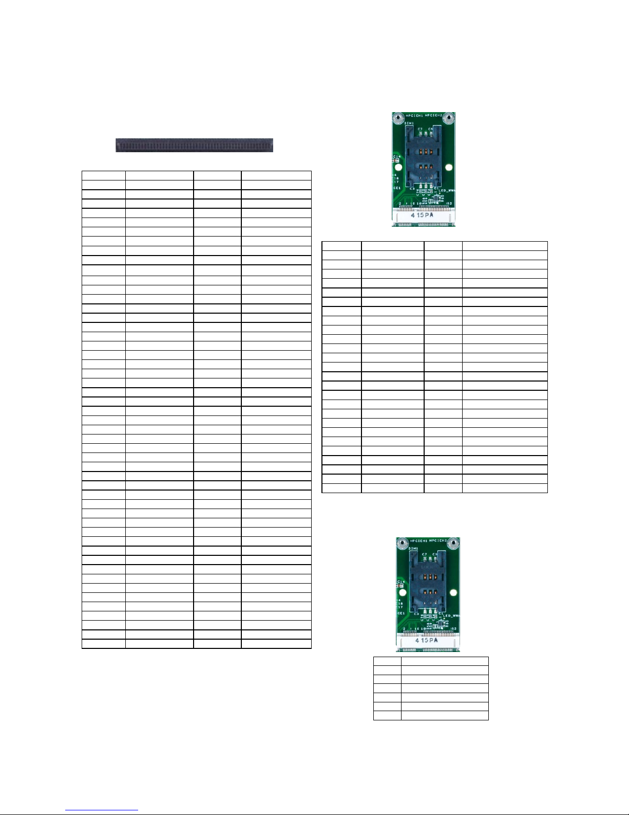
LVK-CBPE1 Board
MIO3: 2x50 Dual-Row Socket for any extension board
PIN Pin Name PIN Pin Name
1 GND 51 N/A
2 PCH_SATATXN3 52 N/A
3 PCH_SATATXP3 53 N/A
4 GND 54 N/A
5 PCH_SATARXN3 55 N/A
6 PCH_SATARXP3 56 N/A
7 N/A 57 VCC3P3_SB
8 VCC3P3_PS 58 VCC3P3_SB
9 VCC3P3_PS 59 VCC3P3_SB
10 VCC3P3_PS 60 VCC3P3_SB
11 GND 61 VCC3P3_SB
12 PCH_PCIE_RXN8 62 N/A
13 PCH_PCIE_RXP8 63 N/A
14 PCH_PCIE_TXN8 64 N/A
15 PCH_PCIE_TXP8 65 N/A
16 PCIE_CKN8 66 N/A
17 PCIE_CKP8 67 N/A
18 N/A 68 N/A
19 PLTRST_BUF1_N 69 SMBCLK_RESUME
20 WAKE_N 70 SMBDAT_RESUME
21 N/A 71 N/A
22 N/A 72 N/A
23 N/A 73 N/A
24 N/A 74 N/A
25 VCC5 75 GND
26 VCC5 76 N/A
27 VCC5 77 N/A
28 GND 78 GND
29 N/A 79 N/A
30 N/A 80 N/A
31 N/A 81 N/A
32 N/A 82 N/A
33 GND 83 GND
34 N/A 84 N/A
35 N/A 85 N/A
36 N/A 86 N/A
37 N/A 87 N/A
38 N/A 88 N/A
39 N/A 89 N/A
40 N/A 90 N/A
41 N/A 91 N/A
42 GND 92 GND
43 N/A 93 N/A
44 N/A 94 N/A
45 N/A 95 N/A
46 N/A 96 N/A
47 N/A 97 N/A
48 N/A 98 N/A
49 N/A 99 COM2_SOUT
50 N/A 100 COM2_SIN
MPCIE1: Mini-PCIe Connector with one SIM Card
Reader(SIM1). It supports both Wi-Fi and 3G module.
Pin Signal Pin Signal
1 WAKE_N 2 VCC3.3
3 N/A 4 GND
5 N/A 6 VCC1.5
7 CLKREQ# 8 USIM_PWR
9 GND 10 UIM_DATA
11 PCIE_CLK_N3 12 UIM_CLK
13 PCIE_CLK_P3 14 UIM_RESET
15 GND 16 UIM_VPP
17 RSV 18 GND
19 RSV 20 N/A
21 GND 22 PLTRST
23 PCIE_RX_N3 24 VCC3.3
25 PCIE_RX_P3 26 GND
27 GND 28 VCC1.5
29 GND 30 SMBCLK
31 PCIE_TX_N3 32 SMBDATA
33 PCIE_TX_P3 34 GND
35 GND 36 USB_N8
37 GND 38 USB_P8
39 VCC3.3 40 GND
41 VCC3.3 42 N/A
43 GND 44 N/A
45 RSV 46 N/A
47 RSV 48 VCC1.5
49 RSV 50 GND
51 RSV 52 VCC3.3
SIM Card Socket : SIM card slot within mini PCIe socket
Pin No. Description
C1 UIM_PWR
C2 UIM_RST
C3 UIM_CLK
C5 GND
C6 UIM_VPP
C7 UIM_DAT
Page 33
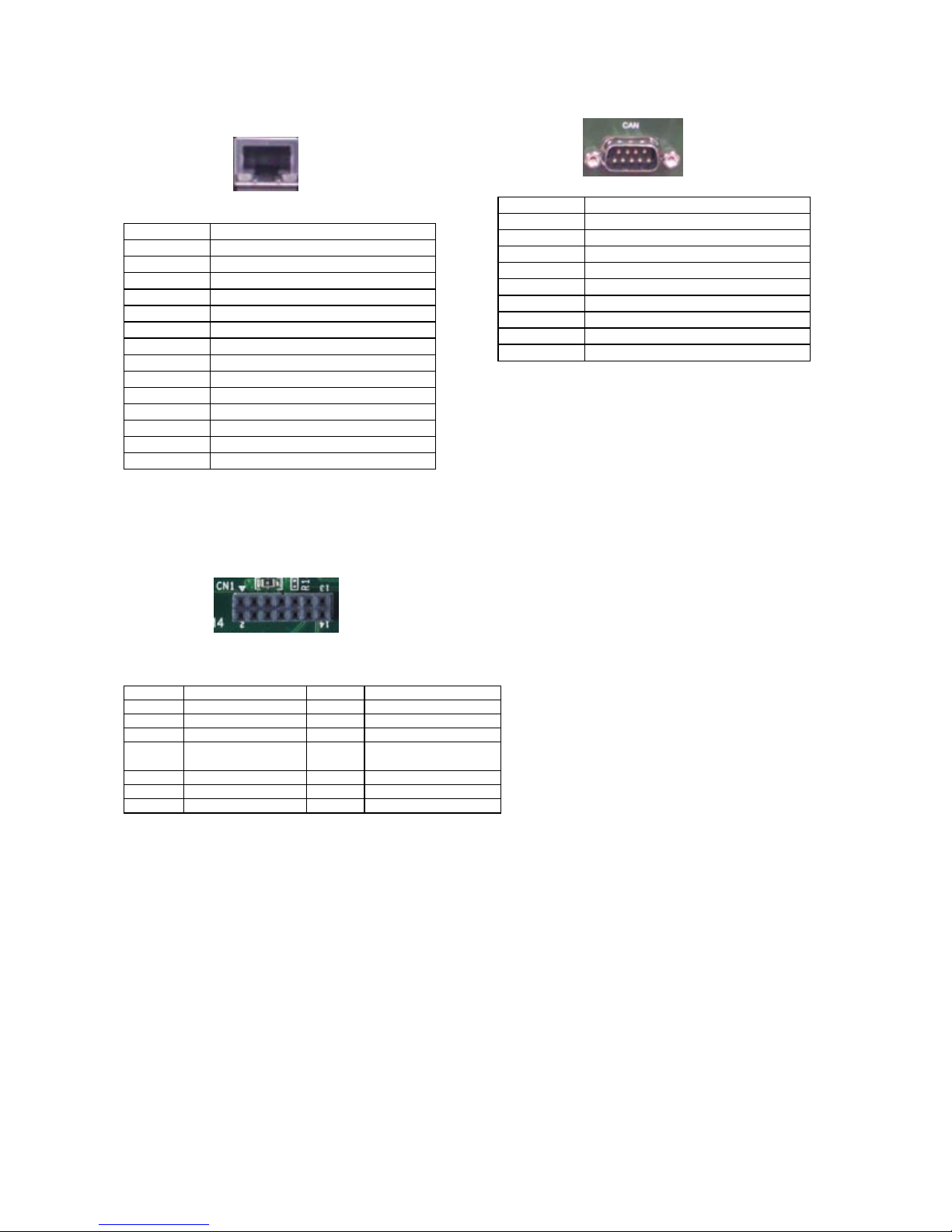
LAN1: Ethernet LAN port on the board
Pin No. Description
1 MDI0P
2 MDI0N
3 MDI1P
4 MDI1N
5 TCL1
6 TCL2
7 MDI2P
8 MDI2N
9 MDI3P
10 MDI3N
11 100_LED
12 1000_LED
13 ACTLED+
14 ACTLED-
CN1: Interpreter Module Connector
Pin Signal Pin Signal
1 Battery 12V/24V In 2 K_LINE
3 DO (Digital Output 4 N/A
5 GND 6 GND
7 Wake up Module
(Optional)
8 J1850+/J1708+
9 UART TX 10 J1850-/J170811 UART RX 12 CAN_H/J1939+
13 VCC5_PS 14 CAN_L/1939-
CAN1: Vehicle’s Electronic Control Unit Junction (D-sub)
Pin No. Description
1 J1850-/J17082 GND
3 CAN_H/J1939+
4 K_LINE
5 CAN_L/J19396 J1850-/J17087 J1850+/J1708+
8 J1850+/J1708+
9 Battery 12V/24V In
Page 34
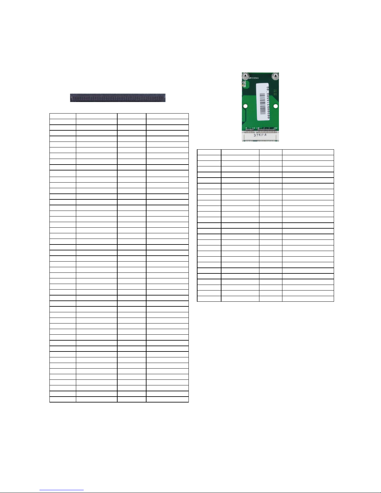
LVK-CBSA1 Board
MIO3: 2x50 Dual-Row Socket for any extension board
PIN Pin Name PIN Pin Name
1 GND 51 N/A
2 PCH_SATATXN3 52 N/A
3 PCH_SATATXP3 53 N/A
4 GND 54 N/A
5 PCH_SATARXN3 55 N/A
6 PCH_SATARXP3 56 N/A
7 N/A 57 VCC3P3_SB
8 VCC3P3_PS 58 VCC3P3_SB
9 VCC3P3_PS 59 VCC3P3_SB
10 VCC3P3_PS 60 VCC3P3_SB
11 GND 61 VCC3P3_SB
12 PCH_PCIE_RXN8 62 N/A
13 PCH_PCIE_RXP8 63 N/A
14 PCH_PCIE_TXN8 64 N/A
15 PCH_PCIE_TXP8 65 N/A
16 PCIE_CKN8 66 N/A
17 PCIE_CKP8 67 N/A
18 N/A 68 N/A
19 PLTRST_BUF1_N 69 SMBCLK_RESUME
20 WAKE_N 70 SMBDAT_RESUME
21 N/A 71 N/A
22 N/A 72 N/A
23 N/A 73 N/A
24 N/A 74 N/A
25 VCC5 75 GND
26 VCC5 76 N/A
27 VCC5 77 N/A
28 GND 78 GND
29 N/A 79 N/A
30 N/A 80 N/A
31 N/A 81 N/A
32 N/A 82 N/A
33 GND 83 GND
34 N/A 84 N/A
35 N/A 85 N/A
36 N/A 86 N/A
37 N/A 87 N/A
38 N/A 88 N/A
39 N/A 89 N/A
40 N/A 90 N/A
41 N/A 91 N/A
42 GND 92 GND
43 N/A 93 N/A
44 N/A 94 N/A
45 N/A 95 N/A
46 N/A 96 N/A
47 N/A 97 N/A
48 N/A 98 N/A
49 N/A 99 COM2_SOUT
50 N/A 100 COM2_SIN
MPCIE1: mSATA slot
Pin Signal Pin Signal
1 N/A 2 VCC3P3_PS
3 N/A 4 GND
5 N/A 6 VCC1P5
7 N/A 8 N/A
9 GND 10 N/A
11 N/A 12 N/A
13 N/A 14 N/A
15 GND 16 N/A
17 N/A 18 GND
19 N/A 20 N/A
21 GND 22 N/A
23 PCH_SATARXP3 24 VCC3P3_PS
25 PCH_SATARXN3 26 GND
27 GND 28 VCC1P5
29 GND 30 SMBCLK_RESUME
31 PCH_SATATXN3 32 SMBDAT_RESUME
33 PCH_SATATXP3 34 GND
35 GND 36 USB12N
37 GND 38 USB12P
39 VCC3P3_PS 40 GND
41 VCC3P3_PS 42 N/A
43 N/A 44 N/A
45 N/A 46 N/A
47 N/A 48 VCC1P5
49 N/A 50 GND
51 N/A 52 VCC3P3_PS
Page 35
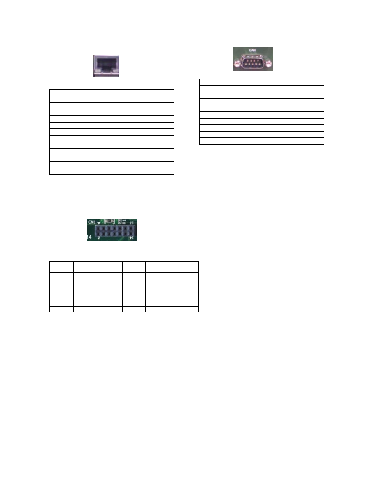
LAN1: Ethernet LAN port on the board
Pin No. Description
1 MDI0P
2 MDI0N
3 MDI1P
4 MDI2P
5 MDI2N
6 MDI1N
7 MDI3P
8 MDI3N
9 ACTLED+
10 ACTLED11 1000_LED
12 100_LED
CN1: Interpreter Module Connector
Pin Signal Pin Signal
1 Battery 12V/24V In 2 K_LINE
3 DO (Digital Output 4 N/A
5 GND 6 GND
7 Wake up Module
(Optional)
8 J1850+/J1708+
9 UART TX 10 J1850-/J170811 UART RX 12 CAN_H/J1939+
13 VCC5_PS 14 CAN_L/1939-
CAN1: Vehicle’s Electronic Control Unit Junction (D-sub)
Pin No. Description
1 J1850-/J17082 GND
3 CAN_H/J1939+
4 K_LINE
5 CAN_L/J19396 J1850-/J17087 J1850+/J1708+
8 J1850+/J1708+
9 Battery 12V/24V In
Page 36
Chapter 4:
Hardware Setup
Preparing the Hardware Installation
WARNING: To reduce the risk of personal injury,
electric shock, or damage to the equipment,
please make sure the device is totally powered
off and without any power source connected.
LVC-5000-B series models are designed with externally
accessible components, which do not require users to
remove the chassis except PCIe modules. Please see the
following for instructions.
Installing a CompactFlash Card
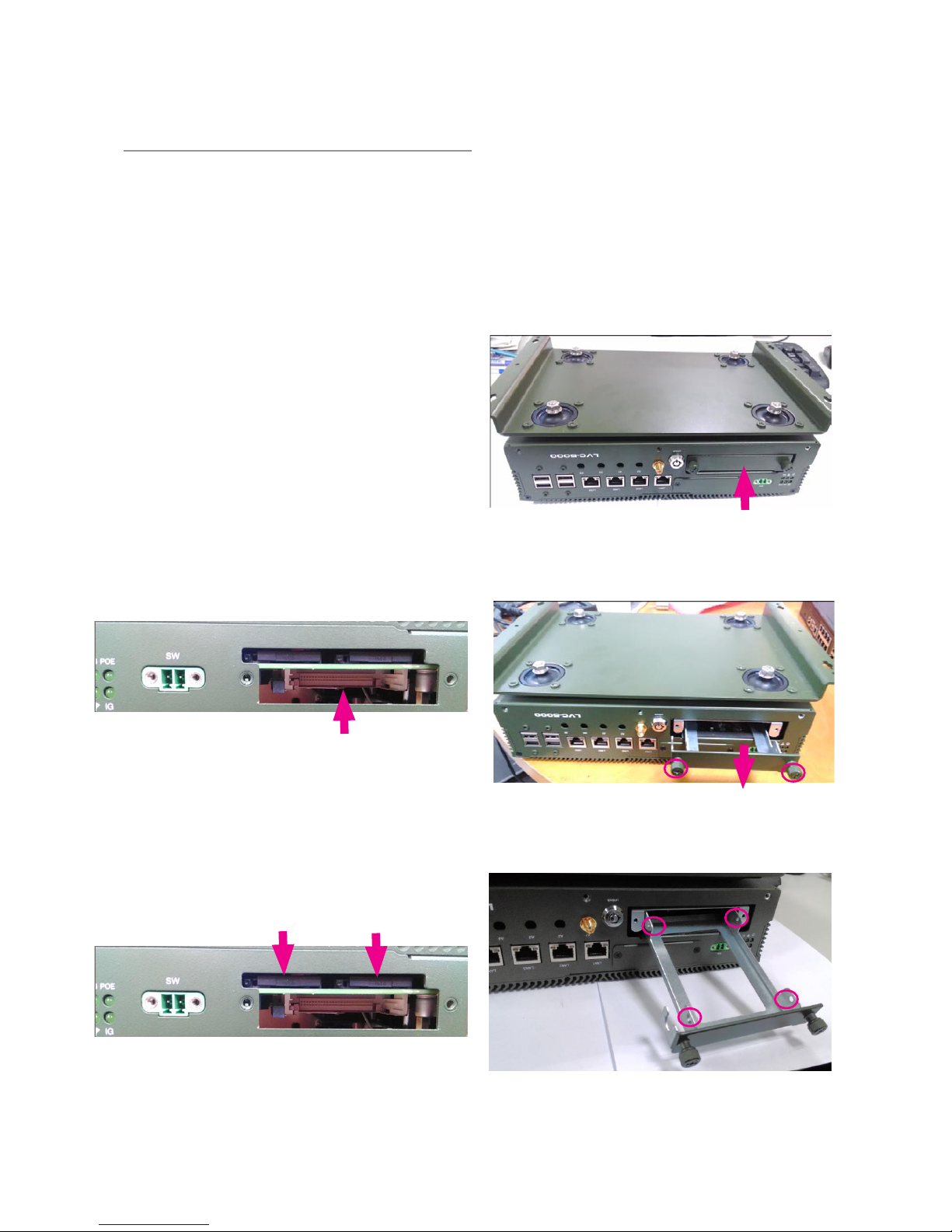
The system comes with an external SIM/CF card slot to
install a CompactFlash card. Simply remove the two mini
screws of this slot. You may refer to “Front Components”
in Chapter 2 for locating this slot.
SIM Card Installation
Locate the SIM/CF card slot on the front panel and 1.
remove the two mini screws.
Align the SIM card in correct direction..2.
Installing a HDD/SSD Disk Drive
The system provides an externally accessible 2.5” SATA
disk drive tray. Please see the instructions below for
installation.
Locate the 2.5” SATA disk drive tray on the front 1.
panel.
Turn the system upside down.2.
3. Loosen the two mini lock-screws and pull the tray
out.
4. Secure your disk drive with 4 screws.
Page 37
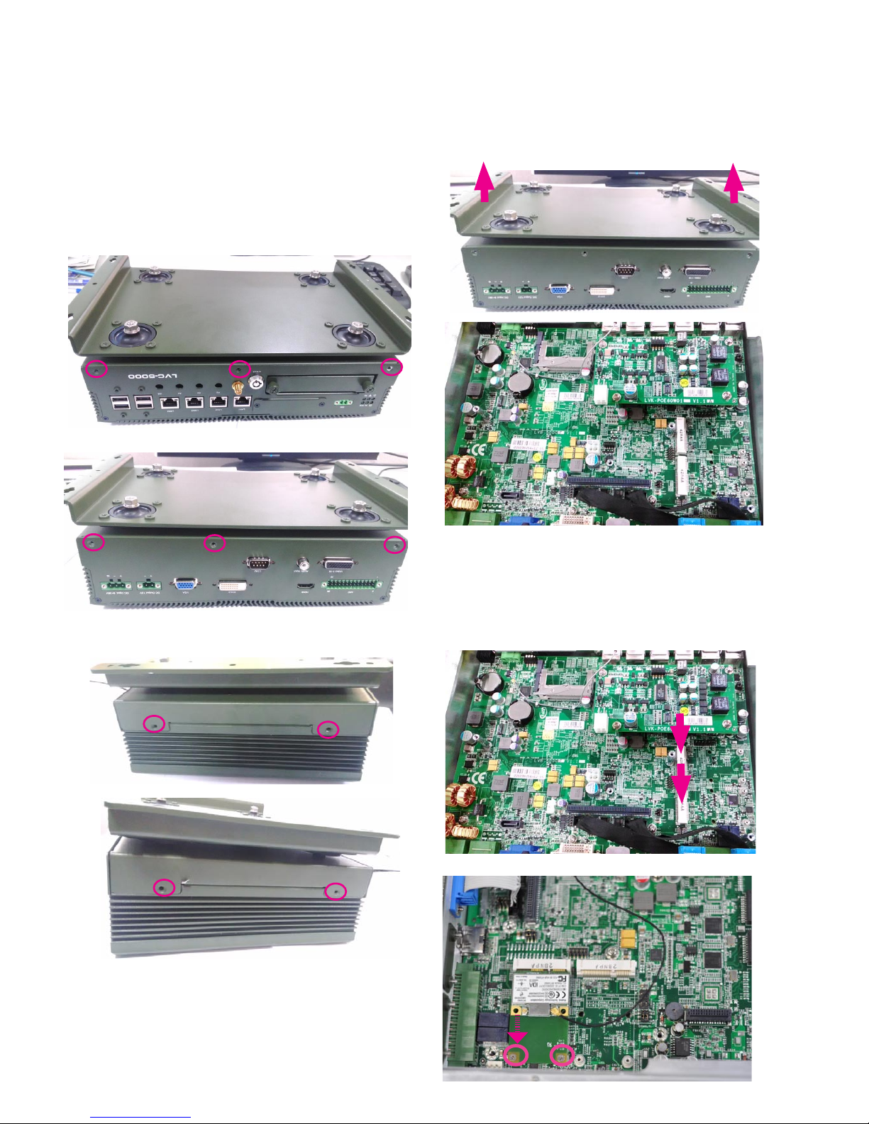
Mini-PCIe Wireless Network Module
Installation
1. Turn the system upside down.
2. Loosen and remove the circled screws on four sides
as circled below.
3. Gently lift the bottom compartment to access the
internal components.
4. Locate the mini-PCIe sockets on the mainboard
5. Align the wireless module’s gold fingers with the
Mini-PCIe slot notch.
6. Insert the wireless module into the connector .
7. Install the module onto the board with the screws.
Page 38
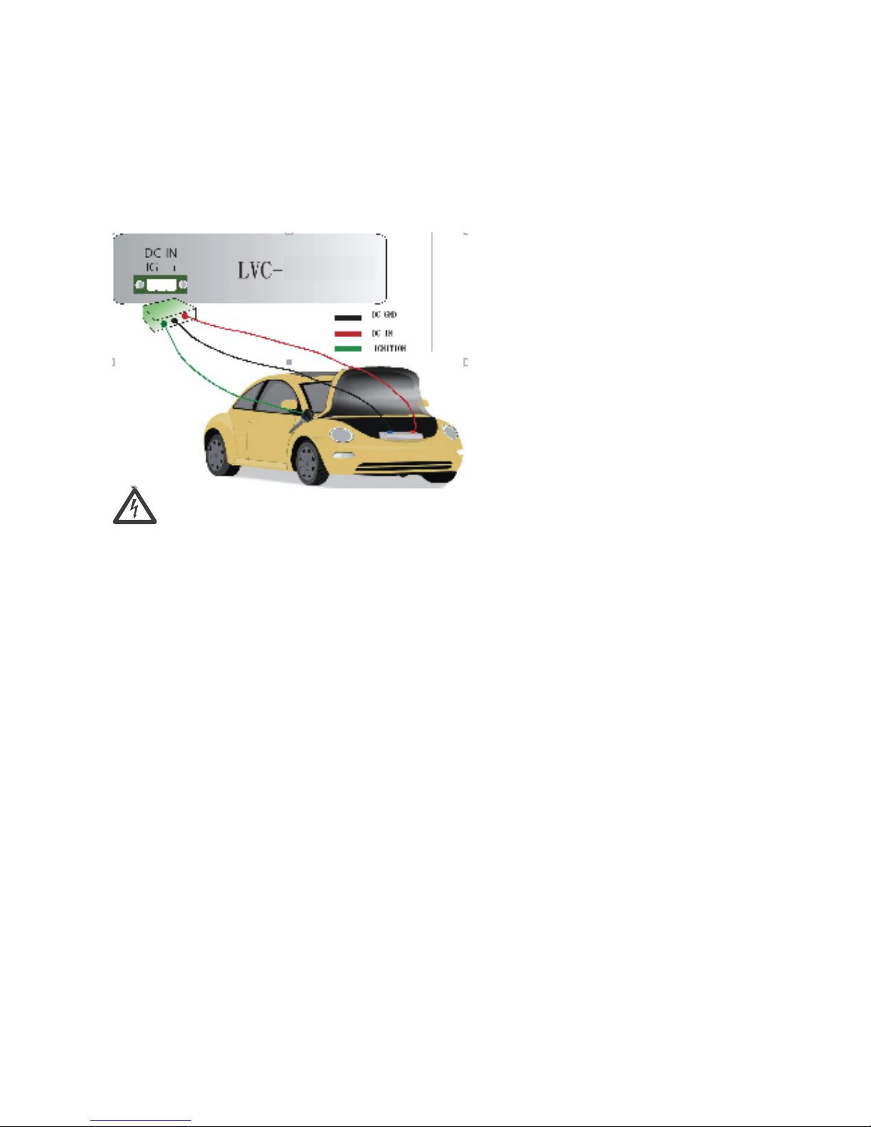
Connecting Power
Connect the LVC-5000 to a +12V or +24V
vehicle battery. The DC power-in connector
comes with a 3-pin terminal block for its Phoenix contact. This power socket can only accept
the power supply with the right pin contact so be
cautious when inserting power to the system.
Warning:
Connect the power to the DC-IN connector in the
right orientation or the LVC-5000 will be damaged.
5000
Notes: This photo images in this chapter are for reference only. The steps of installing components are the same
for all models (B0, B1, B2, and B3) except slight dierences in terms of the number of certain I/O connectors.
Page 39
Chapter 5:
The Flow Chart
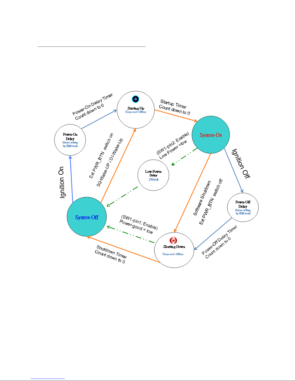
The flow chart section contains all flow chart used in the
system. The flow chart describes the system’s behavior
on powering on and off the system via power ignition
control or on/off switch when the appropriate timer
control parameters are set.
Note:
For power-good and low-voltage
1.
mechanism to function in the workflow,
you will need to enable the power-good
and low-voltage detection function
with selector 1 and selector 2 jumper
respectively of SW1. (Refer to Chapter 3
Board Layout).
For power on and power off delay timer
2.
parameter, refer to Appendix A Using the
Ignition System Manager (ISM).
For DI wake-up function, refer to jumper 3.
MIO2 Pin NO.19 and 21. Refer to Chapter
3 Board Layout and Appendix A Using
the Ignition System Manager (ISM) for
jumper setting and parameter setting
respectively.
When the system’s shutdown timer starts 4.
counting down 180sec, using ignition
or External PWR_BTN to start the system
again during shutdown process will not
work until the countdown finishes.
Page 40
Appendix A:
Using the Ignition System
Manager (ISM)
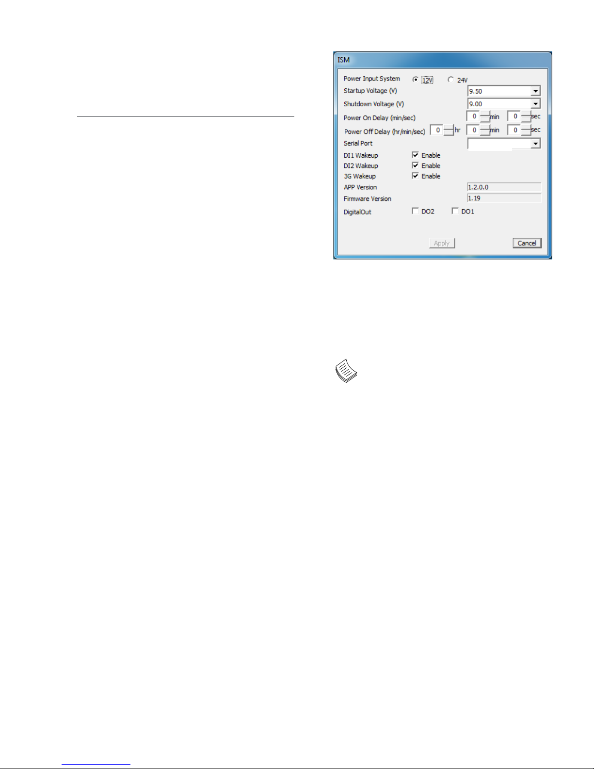
The Ignition System Manager (ISM) is a software that
can monitor the system’s voltage level and configure the
features that the Power Ignition Module provides.
For sample ISM code, see ISM folder under LVC-5000
Utility on the Driver and Manual CD.
Running the Program
Just double click the ISM.exe to launch the ISM.
The program can configure the following values:
Voltage: It shows the current power system.
Power Input System: Select either 12V or 24V for
vehicular power input.
Startup Voltage (V): If the DC-in voltage is not higher
than this value, the system will not be able to start up.
Shutdown Voltage (V): If the DC-in voltage is lower than
the shutdown voltage, the system will start shutdown
process automatically. (Refer to selector 2 of SW1 dip
switch on the mainboard.)
Power-on Delay (min/sec): Select power-on delay value
to indicate the time to delay powering on the system.
(Refer to the flow chart in Chapter 4)
Power-off Delay (hr/min/sec): Select power-off delay
value to indicate the time to delay powering off the
system (Refer to the flow chart in Chapter 4)
Serial Port: Select the serial communication port for the
ISM. Choose COM5.
D1/D2 Wakeup: Digital input triggering to enable
automatic wake-up function. Select this option and it will
start the system automatically once an input has been
triggered.
3G Wakeup: 3G SMS/Ring wake-up to enable automatic
wake-up function. Select this option and it will start the
system automatically through 3G Internet service.
DigitalOut: Check the box to turn on the output device
and check off the box to turn off the connected device.
After you have made changes, click Apply to apply the
changes to the Ignition controller or Cancel to cancel the
changes.
Click Cancel to exit the ISM program.
Note:
You will have to enable (the default is enabled)
1.
the selector 2 (Low Voltage Detection) of SW1 dip
switch on the mainboard to enable automatic
shutdown function. (Refer to Select MCU Detect
Function for power ignition behavior (SW1) in
Chapter 3 Board Layout.)
DI1/DI2 Wakeup function is detected via pin 2.
19/21of MIO2 (Refer to MIO2 in Chapter 3 Board
Layout.)
DO1 function is connected (controlled) via 3. pin
20, 22, 23 while DO2 is connected (controlled) via
pin 24, 25, 26. (Refer to MIO2 in Chapter 3 Board
Layout.)
Refer to the flow charts in Chapter 4 for more
4.
information.
.
COM5
Page 41
Appendix B:
Digital Input/Output
The Digitanl I/O on the rear panel is designed to provide
the input and output operations for the system. For
sample DIO code, see SuperIO folder under LVC-5000
Utility on the Driver and Manual CD. Make sure that
you have installed the Lanner GPIO driver as instructed
below.
Driver Installation
Before you could access or control the operation of
the G-sensor, GPS and Digital I/O functions, install the
the L_IO driver which is the library and driver needed
for Lanner General Purpose Input/Output interface or
functions.
To install the L_IO driver:
Restart the computer, and then log on with 1.
Administrator privileges.
Insert the Drivers and User’s Manual CD to the USB-2.
optical drive.
Browse the contents of the support CD to locate the 3.
file in the LIO folder.
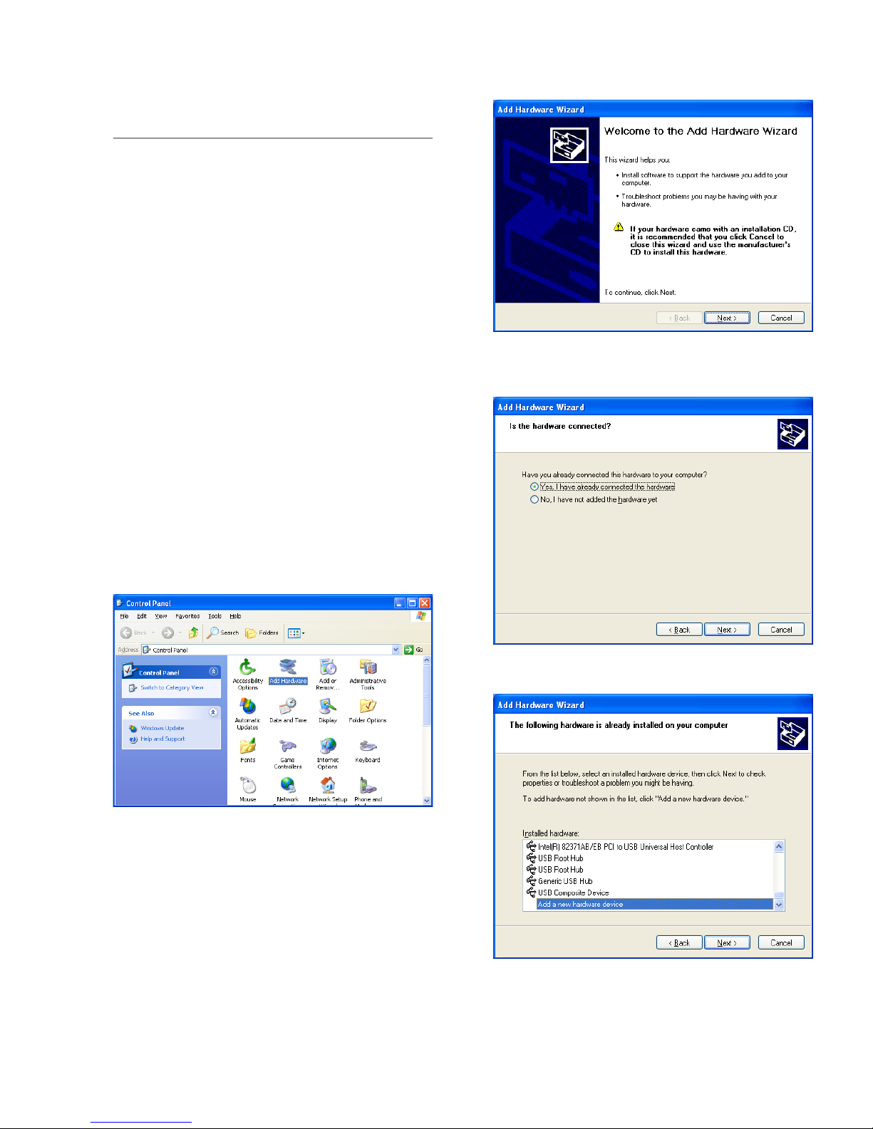
From the control panel, click the ADD Hardware 4.
program
Select Next to proceed5.
Answer “Yes” to the question and select Next to 6.
proceed.
Select Add a new hardware device.7.
Page 42
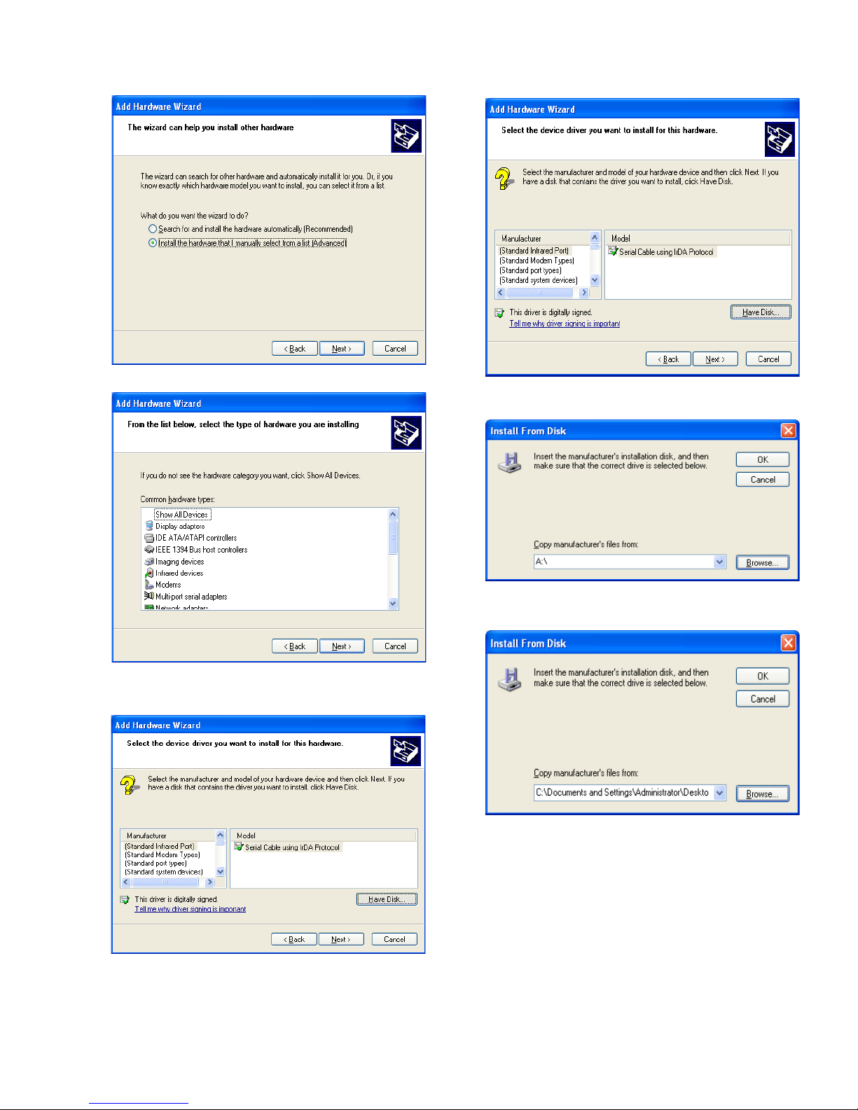
Choose to select the hardware Manually1.
Choose Show all device and click Next.2.
Click HaveDisk to locate the L_IO.inf file3.
Click HaveDisk to locate the L_IO.inf file4.
Select the L_IO.inf5.
Select OK to confirm with the installation6.
Page 43
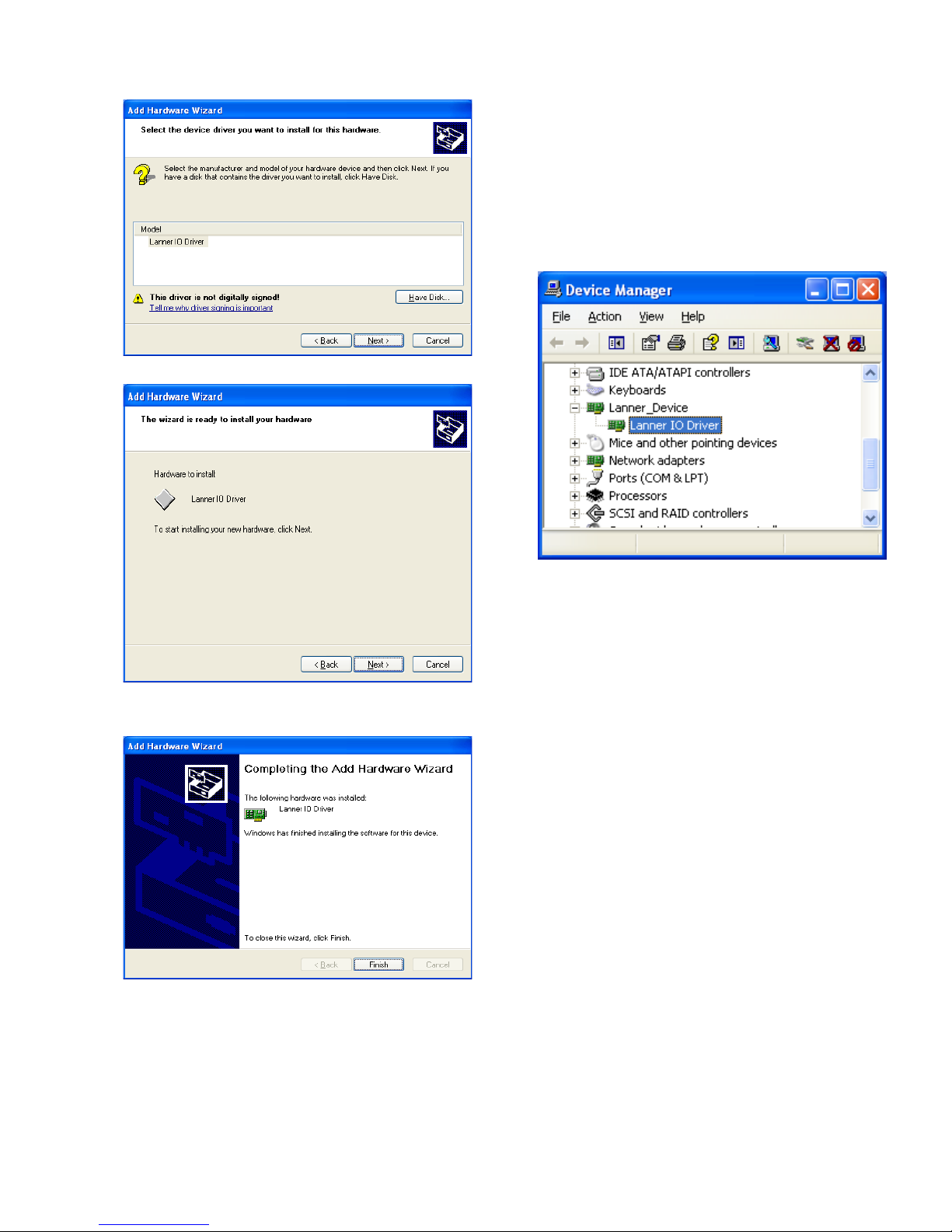
Select the Lanner IO driver and click Next.1.
Click Next2.
Click 3. Complete to close the installation program.
To verify the GPIO driver installation, do the following
steps:
Right-click on the My Computer icon, and then select 1.
Properties form the menu.
Click the Hardware tab, then click the Device Manager 2.
button.
Click the + sign next to the Lanner_Device, then the 3.
Lanner IO Driver should be listed.
Page 44

A sample DIO program in C:
ioaccess.c: IO access code for Lanner Platfomr Digital IO
program
*********************************************************
**********************/
#include “../include/config.h”
#ifdef DJGPP
/* standard include file */
#include <stdio.h>
#include <stdlib.h>
#include <unistd.h>
/* For DOS DJGPP */
#include <dos.h>
#include <inlines/pc.h>
#else //DJGPP
/* For Linux */
#ifdef DIRECT_IO_ACCESS
/* For Linux direct io access code */
/* standard include file */
#include <stdio.h>
#include <stdlib.h>
#include <unistd.h>
#if defined(LINUX_ENV)
#include <sys/io.h>
#endif
#if defined(FreeBSD_ENV)
#include <machine/cpufunc.h>
#endif
#include <time.h>
#include <stdint.h>
#include <fcntl.h>
#include <errno.h>
#include <string.h>
#define delay(x) usleep(x)
#endif
#ifdef MODULE
#include <linux/kernel.h>
#include <linux/module.h>
#include <linux/kernel.h>
#include <linux/fs.h>
#include <asm/io.h>
#include <linux/delay.h>
#undef delay
#define delay(x) mdelay(x)
#undef fprintf
#define fprintf(S, A) printk(A)
#endif //MODULE
#ifdef KLD_MODULE
#include <sys/types.h>
#include <sys/param.h>
#include <sys/systm.h>
#include <sys/malloc.h>
#include <sys/kernel.h>
#include <sys/bus.h>
#include <sys/errno.h>
Page 45

#include <machine/bus.h>
#include <machine/resource.h>
#endif
#endif
/* local include file */
#include “../include/ioaccess.h”
#if (defined(MODULE) || defined(DIRECT_IO_ACCESS) ||
defined(KLD_MODULE))
/*
*-------------------------------------------------------------------------
-----
* LEB-5000 Version V1.0
*output3-0 = GPIO 03-00, input3-0= GPIO 53-50
*--------------------------------------------------------------------------
---------
*/
/*
* Device Depend Definition :
*/
#define INDEX_PORT 0x2E
#define DATA_PORT 0x2F
void enter_SIO_config(void)
{
outportb(INDEX_PORT, 0x87); // Must Do It Twice
outportb(INDEX_PORT, 0x87);
return;
}
void exit_SIO_config(void)
{
outportb(INDEX_PORT, 0xAA);
return;
}
unsigned char read_SIO_reg(int LDN, int reg)
{
outportb(INDEX_PORT, 0x07); //LDN register
delay(5);
outportb(DATA_PORT, LDN);
delay(5);
outportb(INDEX_PORT, reg);
delay(5);
return(inportb(DATA_PORT));
}
void write_SIO_reg(int LDN, int reg, int value)
{
outportb(INDEX_PORT, 0x07); //LDN register
delay(5);
outportb(DATA_PORT, LDN);
delay(5);
outportb(INDEX_PORT, reg);
delay(5);
outportb(DATA_PORT, value);
return;
}
void dio_gpio_init(void)
{
enter_SIO_config();
write_SIO_reg(0x6, 0x30,0x01); //enable GPIO
Port
write_SIO_reg(0x6, 0xf0,((read_SIO_reg(0x6,
0xf0)& 0xF0)|0x0f)); //RxF0[3-0]=1111b, output
write_SIO_reg(0x6, 0xA0, (read_SIO_reg(0x6,
0xA0)& 0xF0)); //RxA0[3-0]=0000b, input
Page 46

exit_SIO_config();
return;
}
void dio_set_output(unsigned char out_value)
{
enter_SIO_config();
write_SIO_reg(0x6, 0xf1, ((read_SIO_reg(0x6,
0xf1)& 0xF0)|out_value));
exit_SIO_config();
return;
}
unsigned int dio_get_input(void)
{
unsigned int tmp=0x00;
enter_SIO_config();
tmp=read_SIO_reg(0x6, 0xA2)& 0x0f;
exit_SIO_config();
return tmp;
}
//======================================
========================================
=================
#endif
Page 47

Appendix C:
Accessing the Digital
Accelerometer Data from
the LVC-5000
The system employs Analog Devices’s ADXL345 Digital
Accelerometer which is a small, thin, ultralow power,
3-axis accelerometer with high resolution (13-bit)
measurement at up to ±16 g. It interfaces with the LVC5000 through a SPI interface.
To access the Gsensor data, locate the adxl345_v001
folder and execute the executable file adxl345 and it will
show G value of 3 axes.
Driver Installation
To access the G-Sensor data, use the following
instructions:
Make sure you already installed the Lanner GPIO 1.
driver on your LVC-5000 as instructed in Appendix B.
To access the Gsensor data, locate the adxl345_v001 2.
folder and execute the executable file adxl345 and it
will show G value of 3 axes.
A sample program in C:++
// main.cpp
// The adxl345.exe utility shows the 3 axis G value.
//
// History:
// 07/15/2011: Initial version
#include <winsock2.h>
#include <windows.h>
#include <stdio.h>
#include “ich7.h”
#include “adxl345.h”
void adxl345_init()
{
ich7_SM_WriteByte (0x1D, POWER_CTL, ACT_INACT_
SERIAL | MEASURE) ; // Power CTL:
Measure mode, Activity and Inactivity Serial
ich7_SM_WriteByte (0x1d, BW_RATE, RATE_100);
//
Output Data Rate: 100Hz
ich7_SM_WriteByte (0x1d, DATA_FORMAT, FULL_
RESOLUTION | DATA_JUST_LEFT | RANGE_16G);
//
Data Format: 16g range, right justified, 256->1g
}
int main(int argc, char* argv[])
{
adxl345_init () ;
while (1)
{
short x = (short) ich7_SM_ReadByte
(0x1d, DATAX1) << 8 | ich7_SM_ReadByte (0x1d,
DATAX0)<<0 ;
short y = (short) ich7_SM_ReadByte
(0x1d, DATAY1) << 8 | ich7_SM_ReadByte (0x1d,
DATAY0)<<0 ;
short z = (short) ich7_SM_ReadByte
(0x1d, DATAZ1) << 8 | ich7_SM_ReadByte (0x1d,
DATAZ0)<<0 ;
printf (“\rX=%.2f Y=%.2f Z=%.2f”, ((float)
x)/2048,((float)y)/2048,((float)z)/2048) ;
}
}
Page 48
Appendix D:
Accessing the GPS Data
from the LVC-5000
The LVC-5000 employs GPS module from GPS ublox NEO6Q for vehicle tracking and navigation system. You could
read the GPS data through the RS-232 serial port.
It has the following listed key features and performance
ratings of the GPS ublox NEO-6Q:
Receiver type 50 Channels
GPS L1 frequency, C/A
Code
SBAS: WAAS, EGNOS,
MSAS
Time-To-First-Fix (All
satellites at -130 dBm)
Cold Start: 26 s
Warm Start: 26 s
Hot Start: 1 s
Aided Starts: 1 s
Sensitivity Tracking &Naviga-•
tion: -161dBm
Reacquisition: •
-160dBm
Cold Start (without •
aiding): -148 dBm
Maximum Navigation
update rate
5Hz
Horizontal position accurach (CEP, 50%, 24
hours static, -130dBm)
GPS: 2.5m
GPS+SBAS: 2.0m
Congurable
Timepulse frequency
range
0.25 Hz to 1 kHz
Accuracy for
Timepulse signal
RMS: 30 ns
99%: <60 ns
Granularity: 21 ns
Velocity accuracy 0.1m/s
Heading accuracy 0.5 degrees
Operational Limits Dynamics: less than and
equal to 4g
Altitude: 50,000m
Velocity: 500m/s (As-
suming Airborne <4g
platform)
To access the GPS data, follow the following steps:
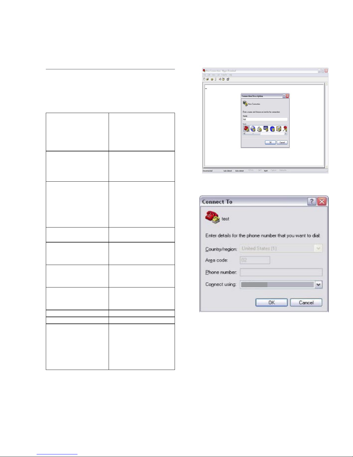
Select Programs from the Start menu on your windows
and open the Hyper Terminal program.
Choose COM4 from the Connection using drop-down
menu:
COM6
Page 49
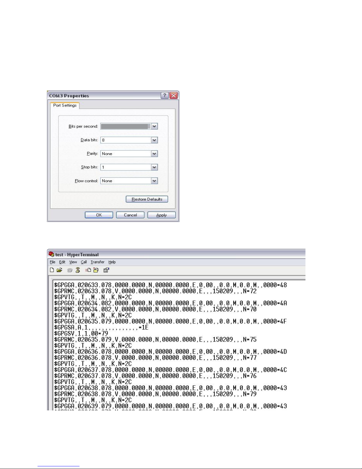
Specify the following communication parameters:
Bits per Second: 9600
Data Bits: 8
Parity: None
Stop Bit: 1
Flow Control: None
The hyper terminal should display GPS data:
9600
Page 50
Appendix E:
Programming System
Watchdog Timer of the
LVC-5000-B
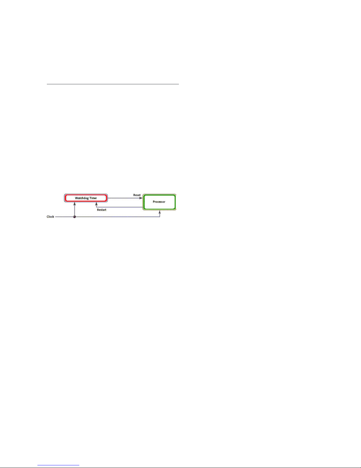
A watchdog timer is a piece of hardware that can be
used to automatically detect system anomalies and reset
the processor in case there are any problems. Generally
speaking, a watchdog timer is based on a counter that
counts down from an initial value to zero. The software
selects the counter’s initial value and periodically restarts
it. Should the counter reach zero before the software
restarts it, the software is presumed to be malfunctioning
and the processor’s reset signal is asserted. Thus, the
processor will be restarted as if a human operator had
cycled the power.
For sample watchdog code, see watchdog folder under
LVC-5000 Utility on the Driver and Manual CD
Executing through the Command Line:
Execute the WD.EXE file under DOS (WD.EXE and
CWSDPMI.EXE should be placed on same directory),
then enter the values from 0~255. The system will reboot
automatically according to the time-out you set.
/////////////////////////////////////////////////////////
You can write your own program by modifying the
source code F81865_Test.cpp.. The index address is 2EH.
////////////////////////////////////////////////////////////////////
/////
// F81865_Test.cpp : F81865_test.exe utility for F81865.lib
APIs demonstration.
//
// History:
// 7/15/2011 Brand new F81865_test
program.
#include <winsock2.h>
#include “Windows.h”
#include “stdio.h”
#include “F81865.h”
#define PARAMETER_HELP “\n”\
“The F81865 GPIO utility of Lanner\n”\
“-------------------------------------\n”\
“Usage:\n”\
“ F81865_test DIO_IN port_
number\n”\
“ F81865_test DIO_OUT port_
number value\n”\
“ F81865_test PIO port_number
value\n”\
“ F81865_test RunLED port_
number value\n”\
“ F81865_test AlarmLED port_
number value\n”\
“ F81865_test GPS_LED port_
number value\n”\
“ F81865_test WirelessLED port_
number value\n”\
“ F81865_test WatchDog seconds\n”\
“ F81865_test CaseOpen\n”\
“ F81865_test CaseOpen_Clear\n”\
“ F81865_test Sleep
milliseconds\n”\
“\n”\
“Argement:\n”\
“ DIO_IN Read state from DIO
In.\n”\
“ DIO_OUT Set DIO Out state.\n”\
“ PIO Set PIO LED state.\n”\
“ RunLED Set RUN LED state.\n”\
“ AlarmLED Set Alarm LED state.\n”\
“ GPS_LED Set GPS LED state.\n”\
“ WirelessLED Set Wireless LED state.\n”\
Page 51

“ Watchdog Set
Watchdog timer.\n”\
“
CaseOpen Check case opened state.\n”\
“
CaseOpen_Clear Clear case open state.\n”\
“ port_number The port number.\n”\
“ value 1 for on and 0 for off.\n”\
“ seconds The
watchdog count down seconds. 0 for disable.\n”\
“ milliseconds Milliseconds to delay\n”
#define RETMSG(a,b) {printf (b) ; return a;}
#define CHECK_ARGC(a) {if (argc != a) throw PARAMETER_HELP ;}
// Translate Hex string to a long value
LONG Hex2Long (char *str)
{
LONG nLong ;
if (scanf (str, “%x”, &nLong) != 1)
throw “Error parsing parameter\n” ;
return nLong ;
}
// Make sure the argument is numeric
void CheckNumeric (char *szBuf)
{
int nLen = strlen (szBuf ) ;
for (int i = 0 ; i < nLen ; i++)
if (!strchr (“01234567890ABCDEFabcdef”, szBuf[i]) )
throw “Wrong argument\n” ;
}
// Common GPIO output function definition
#define GPIO_OUT(a,b,c) \
int a (int argc, char *argv[]) \
{
\
CHECK_ARGC (4) ; \
CheckNumeric (argv[2]) ; \
CheckNumeric (argv[3]) ; \
\
int nPort = atoi (argv[2]) ; \
int nValue = atoi (argv[3]) ; \
\
c (nPort, nValue) ;
\
\
printf (b “ #%d = %d\n”, nPort, nValue) ; \
\
return 0 ;
\
}
// Function generate by common function definition
GPIO_OUT (mDIO_OUT , “DIO_OUT” ,
Write_DIO)
GPIO_OUT (mPIO , “DIO_OUT”
, PIO)
GPIO_OUT (mRunLED , “RunLED” ,
RunLED)
GPIO_OUT (mAlarmLED , “AlarmLED” ,
AlarmLED)
GPIO_OUT (mGPS_LED , “GPS_LED” ,
GPS_LED)
GPIO_OUT (mWirelessLED , “WirelessLED” ,
WirelessLED)
// Check case open
int mCaseOpen (int argc, char* argv[])
{
CHECK_ARGC (2) ;
BOOL bOpen = CaseOpen () ;
printf (“Case is %s\n”, bOpen ? “Open” : “Close”) ;
return bOpen ;
}
Page 52

// Clear case open state
int mCaseOpen_Clear (int argc, char* argv[])
{
CHECK_ARGC (2) ;
CaseOpen_Clear () ;
BOOL bOpen = CaseOpen () ;
printf (“CaseOpen state %s”, bOpen ? “not cleared” :
“cleared”) ;
return bOpen ;
}
// Get DIO_IN state
int mDIO_IN (int argc, char* argv[])
{
CHECK_ARGC (3) ;
CheckNumeric (argv[2]) ;
int nPort = atoi (argv[2]) ;
BOOL ret = Read_DIO (nPort) ;
printf (“DIO_IN #%d = %d\n”, nPort, ret) ;
return ret ;
}
// Milli-second delay
int mSleep (int argc, char *argv[])
{
CHECK_ARGC (3) ;
CheckNumeric (argv[2]) ;
Sleep (atoi (argv[2]) ) ;
return 0 ;
}
// Watchdog
int mWatchDog (int argc, char *argv[])
{
if (argc != 3 && argc != 2)
RETMSG (-1, PARAMETER_HELP) ;
if (argc == 3)
{
CheckNumeric (argv[2]) ;
int nValue = atoi (argv[2]) ;
WatchDog_Enable (nValue) ;
}
int nLeft = WatchDog_GetLeft () ;
printf (“Watchdog timer left %d seconds\n”, nLeft) ;
return nLeft ;
}
// Argument - function mapping
typedef struct
{
char *szCmd ;
int (*function) (int argc, char *argv[]) ;
} CMD2FUN ;
CMD2FUN c2f[] =
{
Page 53

{“DIO_IN” , mDIO_IN
},
{“DIO_OUT” , mDIO_OUT
},
{“PIO” , mPIO
},
{“RunLED” , mRunLED
},
{“AlarmLED” , mAlarmLED
},
{“GPS_LED” , mGPS_LED
},
{“WirelessLED” , mWirelessLED },
{“CaseOpen” , mCaseOpen },
{“CaseOpen_Clear”,mCaseOpen_Clear},
{“Watchdog” , mWatchDog
},
{“Sleep” , mSleep }
} ;
// Program start here
int main(int argc, char *argv[])
{
try
{
// The total argument allowed
int num = sizeof (c2f ) / sizeof (c2f[0]) ;
// Too few argument
if (argc < 2)
RETMSG (-1, PARAMETER_
HELP) ;
// Find the match argument and
execute the mapping function
for (int i = 0 ; i < num ; i++)
if (stricmp (argv[1], c2f[i].
szCmd) == 0)
return c2f[i].function
(argc, argv) ;
// No match argument
RETMSG (-1, “Wrong Argument\n”) ;
}
catch (char *str)
{
// Output the error message
printf (“\n%s\n”, str) ;
}
catch (...)
{
// Unknown exception
printf (“\nUnknown Exception\n”) ;
}
return -1 ;
}
Page 54

Appendix F:
Terms and Conditions
Warranty Policy
All products are under warranty against defects in 1.
materials and workmanship for a period of one year
from the date of purchase.
The buyer will bear the return freight charges for 2.
goods returned for repair within the warranty period;
whereas the manufacturer will bear the after service
freight charges for goods returned to the user.
The buyer will pay for repair (for replaced 3.
components plus service time) and transportation
charges (both ways) for items after the expiration of
the warranty period.
If the RMA Service Request Form does not meet the 4.
stated requirement as listed on “RMA Service,” RMA
goods will be returned at customer’s expense.
The following conditions are excluded from this 5.
warranty:
Improper or inadequate maintenance by the customer
Unauthorized modification, misuse, or reversed
engineering of the product Operation outside of the
environmental specifications for the product.
RMA Service
Requesting a RMA#
To obtain a RMA number, simply fill out and fax the 6.
“RMA Request Form” to your supplier.
The customer is required to fill out the problem code 7.
as listed. If your problem is not among the codes
listed, please write the symptom description in the
remarks box.
Ship the defective unit(s) on freight prepaid terms. 8.
Use the original packing materials when possible.
Mark the RMA# clearly on the box. 9.
Note: Customer is responsible for shipping
damage(s) resulting from inadequate/loose
packing of the defective unit(s). All RMA# are
valid for 30 days only; RMA goods received after
the effective RMA# period will be rejected.
Page 55
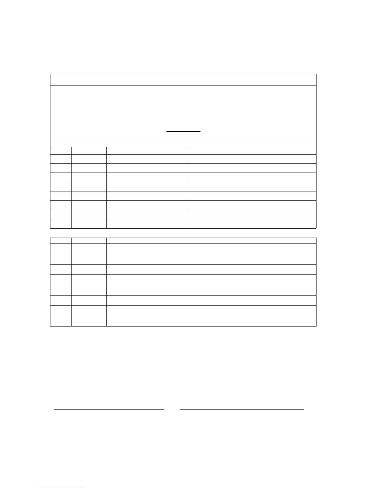
RMA Service Request Form
When requesting RMA service, please fill out the following form. Without
this form enclosed, your RMA cannot be processed.
RMA No:
Reasons to Return: Ŀ Repair(Please include failure details)
Ŀ Testing Purpose
Company: Contact Person:
Phone No. Purchased Date:
Fax No.: Applied Date:
Return Shipping Address:
Shipping by: Ŀ Air Freight Ŀ Sea Ŀ Express ___
Ŀ Others:________________
Item Model Name Serial Number Configuration
Item Problem Code Failure Status
*Problem Code:
01:D.O.A.
02: Second Time
R.M.A.
03: CMOS Data Lost
04: FDC Fail
05: HDC Fail
06: Bad Slot
07: BIOS Problem
08: Keyboard Controller Fail
09: Cache RMA Problem
10: Memory Socket Bad
11: Hang Up Software
12: Out Look Damage
13: SCSI
14: LPT Port
15: PS2
16: LAN
17: COM Port
18: Watchdog Timer
19: DIO
20: Buzzer
21: Shut Down
22: Panel Fail
23: CRT Fail
24: Others (Pls specify)
Request Party
Confirmed By Supplier
Authorized Signature / Date Authorized Signature / Date
 Loading...