

Page 1

UE9 Product Page
Published on LabJack (http://labjack.com)
Home > UE9 User's Gui de
UE9 User's Guide
This is the complete user's guide for the UE9, including documentation for the LabJackUD driver.
Includes specifications in Appendix A.
To make a PDF of the whole manual, click "Export all" towards the upper-right of this page. Doing so
converts these pages to a PDF on-the-fly, using the latest content, and can take 20-30 seconds.
Make sure you have a current browser (we mostly test in Firefox and Chrome) and the current version
of Acrobat Reader. If it is not working for you, rather than a normal click of "Export all" do a right-click
and select "Save link as" or similar. Then wait 20-30 seconds and a dialog box will pop up asking
you where to save the PDF. Then you can open it in the real Acrobat Reader, not embedded in a
browser. If you still have problems, try the "Print all" option instead. In addition, an export is attached
below, but will not always be the latest version.
If you are looking at a PD F or hardcopy, realize that the original is an online document at http://labjack.com/support/ue9/usersguide.
Rather than using a PDF, though, we encourage you to use this web-based documentation. Some advantages:
We can quickly change or update content.
The site search includes the user's guide, forum, and all other resources at labjack.com. When you are looking for
something try using the site search.
For support, try going to the applicable user's guide page and post a comment. When appropriate we can then immediately
add/change content on that page to address the question.
One other trick worth mentioning, is to browse the table of contents to the left. Rather than clicking on all the links to browse, you
can click on the small black triangles to expand without reloading the whole page.
User's Guide
File attachment:
UE9_UG_Export_04282011.pdf
Preface
For the latest version of this and other documents, go to www.labjack.com.
Copyright 2012, LabJack Corporation
Package Contents:
The normal retail packaged UE9 or UE9-Pro consists of:
UE9 (-Pro) unit itself in red enclosure
USB cable (6 ft / 1.8 m)
Ethernet cable (6 ft / 1.8 m)
Power supply
Screwdriver
1
Page 2

Warranty:
The LabJack UE9 is covered by a 1 year limited warranty from LabJack Corporation, covering this product and parts against
defects in material or workmanship. The LabJack can be damaged by misconnection (such as connecting 120 VAC to any of the
screw terminals), and this warranty does not cover damage obviously caused by the customer. If you have a problem, contact
support@labjack.com for return authorization. In the case of warranty repairs, the customer is responsible for shipping to LabJack
Corporation, and LabJack Corporation will pay for the return shipping.
Limitation of Liability:
LabJack designs and manufactures measurement and automation peripherals that enable the connection of a PC to the realworld. Although LabJacks have various redundant protection mechanisms, it is possible, in the case of improper and/or
unreasonable use, to damage the LabJack and even the PC to which it is connected. LabJack Corporation will not be liable for
any such damage.
Except as specified herein, LabJack Corporation makes no warranties, express or implied, including but not limited to any implied
warranty or merchantability or fitness for a particular purpose. LabJack Corporation shall not be liable for any special, indirect,
incidental or consequential damages or losses, including loss of data, arising from any cause or theory.
LabJacks and associated products are not designed to be a critical component in life support or systems where malfunction can
reasonably be expected to result in personal injury. Customers using these products in such applications do so at their own risk
and agree to fully indemnify LabJack Corporation for any damages resulting from such applications.
LabJack assumes no liability for applications assistance or customer product design. Customers are responsible for their
applications using LabJack products. To minimize the risks associated with customer applications, customers should provide
adequate design and operating safeguards.
Reproduction of products or written or electronic information from LabJack Corporation is prohibited without permission.
Reproduction of any of these with alteration is an unfair and deceptive business practice.
Conformity Information (FCC, CE, RoHS):
See the Conformity Page and the text below:
FCC PART 15 STATEMENTS:
This equipment has been tested and found to comply with the limits for a Class B digital device, pursuant to Part 15 of the FCC
Rules. These limits are designed to provide reasonable protection against harmful interference when the equipment is operated in
a commercial environment. This equipment generates, uses, and can radiate radio frequency energy and, if not installed and used
in accordance with the instruction manual, may cause harmful interference to radio communications. Operation of this equipment
in a residential area is likely to cause harmful interference in which case the user will be required to correct the interference at his
own expense. The end user of this product should be aware that any changes or modifications made to this equipment without the
approval of the manufacturer could result in the product not meeting the Class B limits, in which case the FCC could void the user's
authority to operate the equipment.
Declaration of Conformity:
Manufacturers Name: LabJack Corporation
Manufacturers Address: 3232 S Vance St STE 100, Lakewood, CO 80227, USA
Declares that the product
Product Name: LabJack UE9 (-Pro)
Model Number: LJUE9 (-Pro)
conforms to the following Product Specifications:
EN 55011 Class B
EN 61326-1: 2002 General Requirements
and is marked with CE
RoHS:
The UE9 (-Pro) is RoHS compliant per the requirements of Directive 2002/95/EC.
1 - Installation on Windows
The LJUD driver requires a PC running Windows. For other operating systems, go to labjack.com for available support. Software
2
Page 3
will be installed to the LabJack directory which defaults to c:\Program Files\LabJack\.
Install the software first: Go to labjack.com/support/ue9.
Connect the USB cable: (See Section 2.2 for Ethernet installation tips) The USB cable provides data and power. After the UD
software installation is complete, connect the hardware and Windows should prompt with “Found New Hardware” and shortly after
the Found New Hardware Wizard will open. When the Wizard appears allow Windows to install automatically by accepting all
defaults.
Run LJControlPanel: From the Windows Start Menu, go to the LabJack group and run LJControlPanel. Click the “Find Devices”
button, and an entry should appear for the connected UE9 showing the serial number. Click on the “USB – 1” entry below the serial
number to bring up the UE9 configuration panel. Click on “Test” in the configuration panel to bring up the test panel where you can
view and control the various I/O on the UE9.
If LJControlPanel does not find the UE9, check Windows Device Manager to see if the UE9 installed correctly. One way to get to
the Device Manager is:
Start => Control Panel => System => Hardware => D evice Manager
The entry for the UE9 should appear as in the following figure. If it has a yellow caution symbol or exclamation point symbol, rightclick and select “Uninstall” or “Remove”. Then disconnect and reconnect the UE9 and repeat the Found New Hardware Wizard as
described above.
1.1 - Control Panel Application (LJControlPanel)
The LabJack Control Panel application (LJCP.exe) handles configuration and testing of the UE9. Click on the “Find LabJacks”
button to search for connected devices.
Figure 1-1. LJControlPanel Main Window
Figure 1-1 shows the results from a typical search. The application found one UE9 connected by USB and Ethernet. It also found a
second UE9 that is accessible only by Ethernet. The USB connection has been selected in Figure 1-1, bringing up the
configuration window on the right side.
Refresh: Reload the window using values read from the device.
Write to Device: Write the values from the window to the device. Depending on the values that have been changed, the
3
Page 4
application might prompt for a device reset.
Reset: Click to reset the selected device.
Test: Opens the window shown in Figure 1-2. This window continuously writes to and reads from the selected LabJack.
Figure 1-2. LJControlPanel Test Window
Selecting Options=>Settings from the main LJControlPanel menu brings up the window shown in Figure 1-3. This window allows
some features to of the LJControlPanel application to be customized.
Figure 1-3. LJControlPanel Settings Window
Search for USB devices: If selected, LJControlPanel will include USB when searching for devices.
Search for Ethernet devices using UDP broadcast packet: Normally, Ethernet connected devices are found using a
broadcast of the DiscoveryUDP command documented in Section 5.2.3. On some networks, however, it might not be
desirable to broadcast these UDP packets. There are also situations where a network might have proper TCP
communication between the PC and LabJack, but the broadcast UDP packet does not work.
Search for Ethernet devices using specified IP addresses. When this option is selected, LJControlPanel will specifically
search over TCP using each address in the list. On some networks this might be preferred over the UDP broadcast search.
1.2 - Self-Upgrade Application (LJSelfUpgrade)
Both processors in the UE9 have field upgradeable flash memory. The self-upgrade application shown in Figure 1-4 programs the
latest firmware onto either processor.
First, put valid values in the “Connect by” box. If USB, select first found or specify a local ID. If Ethernet, specify the IP Address.
These values will be used for programming and everything else.
Click on “Get Version Numbers”, to find out the current firmware versions on the device. Then use the provided Internet link to go to
labjack.com and check for more recent firmware. Download firmware files to the …\LabJack\LJSelfUpgrade\upgradefiles\
directory.
Click the Browse button and select the upgrade file to program. Based on the file name, the application will determine whether the
4
Page 5
Comm or Control processor is to be programmed.
Click the Program button to begin the self-upgrade process.
Figure 1-4. Self-Upgrade Application
If problems are encountered during programming, try the following:
1. Unplug the UE9, wait 5 seconds then reconnect the UE9. Click OK then press program again.
2. If step 1 does not fix the problem unplug the UE9 and watch the C ontrol and Control LEDs while plugging the UE9 back in.
Follow the following steps based on the Comm and Control LEDs' activity.
1. If the Comm LED blinks several times and the Control LED is blinking rapidly (flash mode), connect a jumper
between FIO0 and SCL, then unplug the UE9, wait 5 seconds and plug the UE9 back in. Try programming again
(disconnect the jumper before programming).
2. If the Comm LED blinks several times and the Control LED has no activity, connect a jumper between FIO1 and
SCL, then unplug the UE9, wait 5 seconds and plug the UE9 back in. Try programming again (disconnect the jumper
before programming).
3. If the Comm LED has no activity, the UE9's Comm processor is not starting properly. Please restart your computer
and try programming again.
3. If there is no activity from the UE9's LEDs after following the above steps, please contact support.
2 - Hardware Description
The UE9 has 3 different I/O areas:
Communication Edge,
Screw Terminal Edge,
DB Edge.
The communication edge has a USB type B connector (with
black cable connected in Figure 2-1), a 10Base-T Ethernet
connector (with yellow cable connected in Figure 2-1), and two
entry points for external power (screw-terminals or power jack).
The screw terminal edge has convenient connections for 4
analog inputs, both analog outputs, and 4 flexible digital I/O
(FIO). The screw terminals are arranged in blocks of 4, with each
block consisting of Vs, GND, and two I/O. Also on this edge are
two LEDs associated with the two processors in the UE9.
The DB Edge has 2 D-sub type connectors: a DB37 and DB15.
The DB37 has some digital I/O and all the analog I/O. The DB15
has 12 additional digital I/O.
5
Page 6

Figure 2-1. LabJack UE9
2.1 - USB
For information about USB installation, see Section 1.
The UE9 has a full-speed USB connection compatible with USB version 1.1 or 2.0. This connection can provide communication
and power (Vusb), but it is possible that some USB ports will not be able to provide enough power to run the UE9 at all speeds.
Certain low power USB ports can be limited to 100 milliamps, and some power modes of the UE9 use more than 100 milliamps.
A USB hub with a power supply (self-powered) will always provide 500 milliamps for each port.
USB ground is connected to the UE9 ground, and USB ground is generally the same as the ground of the PC chassis and AC
mains. In this case, the UE9 is not electrically isolated when the USB cable is connected.
The details of the UE9 USB interface are handled by the high level drivers (Windows LabJackUD DLL), so the following
information is really only needed when developing low-level drivers.
The LabJack vendor ID is 0×0CD5. The product ID for the U3 is 0×0009.
The USB interface consists of the normal bidirectional control endpoint 0 and two bidirectional bulk endpoints: Endpoint 1 and
Endpoint 2. Endpoint 1 consists of a 16 byte OUT endpoint (address = 0x01) and a 16 byte IN endpoint (address 0x81). Endpoint
2 consists of a 64 byte OUT endpoint (address = 0x02) and a 64 byte IN endpoint (address = 0x82).
Commands can be sent on either endpoint, and the response will be sent on the same endpoint, except that stream data is always
transferred on IN Endpoint 2, regardless of whether the stream start command was sent on OUT Endpoint 1 or 2.
Commands can be sent on both endpoints at the same time, but as with any connection on the UE9, do not send a second
command on an endpoint until after receiving the response to the first command.
Except for reading stream data, always write and read the actual number of bytes in the command and response. If the size is not
an even multiple of the endpoint size a short packet will be transferred. In general, small transfers will be faster on Endpoint 1 and
large transfers will be faster on Endpoint 2, but the time differences are small if any, and it is normal to do all communication
besides reading stream data on Endpoint 1. The main reason for the different endpoints is to simplify calling command/response
functions while a stream is in progress.
USB stream data is a special case where each 46-byte data packet is padded with 2 zeros on the end (not part of the protocol),
and then 4 of these 48-byte blocks are grouped together and sent in 3 transfers over the 64-byte endpoint. The host will generally
read stream data over USB in multiples of 192 bytes (64 samples). This means that at low scan rates there could be a long time
between reads and latency will be high, but this can be improved by oversampling.
The USB transceiver on the UE9 has a 128 byte hardware buffer on Endpoint 2. If the UE9 stream data buffer has one or more
StreamData packets available, they are moved to the USB buffer to await a read by the host. Once placed in this USB buffer, the
data cannot be removed (e.g. by a FlushBuffer command). To avoid confusion on future communication on Endpoint 2, this buffer
should always be emptied after streaming.
One way to empty this buffer is to continue reading data after StreamStop, until there is no more (the read times out). This should
not require a long timeout as the data is not being acquired, but simply waiting to be retrieved from the UE9 FIFO buffer.
Another option is to follow the StreamStop command with a FlushBuffer command. Then just try to read the last 128 bytes that
could still be in the USB buffer.
A third option is to do a StreamStop (and a FlushBuffer if desired), and then do not attempt to empty the USB buffer, but always
discard the first two StreamData packets after StreamStart.
2.2 - Ethernet
The UE9 has a 10Base-T Ethernet connection. This connection only provides communication, so power must be provided by an
external power supply or USB connection.
UE9 commands (Section 5) can all be sent using TCP, except for DiscoveryUDP. All commands, except stream related
commands, can also be sent using UDP.
The Ethernet connection on the UE9 has 1500 volts of galvanic isolation. As long as the USB cable is not connected, the overall
isolation level of the UE9 will be determined by the power supply. All power supplies shipped by LabJack Corporation with the
UE9 have at least 500 volts of isolation.
6
Page 7

See a note about power-over-Ethernet (POE) in Section 2.3.
The UE9 has a 10Base-T Ethernet connection. This connection only provides communication, so power must be provided by an
external power supply or USB connection. The UE9 ships with an Ethernet patch cable that would normally be used to connect to a
hub or switch. A direct connection from the UE9 to a computer might require a crossover cable (not included), but often the
network interface card (NIC) on modern computers is capable of automatically detecting the signal orientation and will work with
either cable type (patch or crossover).
The LEDs on a switch/hub/NIC can be used to determine if you have an electrically valid connection. An orange LED is often used
to indicate a good 10Base-T connection, but consult the manual for the switch/nub/NIC to be sure. In the case of a direct
connection between PC and UE9, if Windows says “A network cable is unplugged” or similar, it suggests that the UE9 is not
powered or the wrong type of cable is connected.
Complex networks might require the assistance of your network administrator to use the UE9, but the following information is often
sufficient for basic networks.
One basic requirement for TCP communication is that the UE9’s IP address must be part of the subnet and not already used.
Open a command prompt window and type “ipconfig” to see a listing of the IP address and subnet mask for a particular PC. If the
PC shows a subnet mask of 255.255.255.0, that means it can only talk to devices with the same first 3 bytes of the IP address.
The default IP address of the UE9 is 192.168.1.209, which will generally work on a network using the 192.168.1.* subnet (unless
another device is already using the .209 address). If the IP address of the UE9 needs to be changed, the easiest way is via USB
with the LJControlPanel application.
LJControlPanel and Ping (open a command prompt window and type “ping 192.168.1.209”) are useful utilities for testing basic
Ethernet communication. It is a good idea to attempt to Ping the desired IP address before connecting the UE9, to see if anything
is already using that address. A more extensive Ethernet troubleshooting utility called UE9ethertest is available. See the file
readme.txt in the UE9ethertest.zip archive for more information.
2.3 - Vext (Screw Terminals and Power Jack)
There are two connections for an external power supply (Vext): a two-pole screw terminal or a 2.1 mm center-positive power jack.
These connections are electrically the same, so generally only one is used at a time.
The nominal power supply voltage for the UE9 is 5 volts. Power can be provided from the USB connection (Vusb) or an external
power supply (Vext). The UE9 has an internal semiconductor switch that automatically selects between Vusb and Vext. Both power
sources can be connected at the same time, and either can be connected/disconnected at any time. As long as one supply
remains valid, the UE9 will operate normally. If both Vusb and Vext are connected and valid, the internal switch will select Vext.
The UE9 power supply requirement is nominally 5 volts at <200 mA (see Appendix A). This is generally provided by a wall-wart or
wall-transformer type of supply. A supply capable of 500 mA is recommended. The power jack connector is 2.1 × 5.5 mm, center
positive. A linear (regulated) or switching supply is acceptable. Switching supplies are generally noisier than linears, but the UE9
is not particularly sensitive to power supply noise, and most users will not notice any difference. One option is the CUI
EMSA050120K-P5P-SZ available from Digikey, for which you will also need a clip: EMS-AU (Australia), EMS-CC (China), EMSEU (Europe), EMS-UK (United Kingdom), or EMS-US (United States).
Another interesting option is a power-over-Ethernet (POE) adapter. The UE9 does not support POE itself, but there are POE
adapters that split out the data and power in such a manner that is acceptable for the UE9. These adapters consist of an injector
and splitter, and a single Ethernet cable carries data and power between the two. LabJack Corporation has done testing with the
WAPPOE unit from Linksys, which is an off-the-shelf POE adapter with the proper connections for a UE9.
2.4 - Comm and Control LEDs
There is a yellow LED associated with the Comm (communication) processor, and a green LED associated with the Control
processor.
The Comm LED flashes on reset and USB enumeration, and then only turns on when there is communication (USB/Ethernet)
traffic. This LED then turns off if there is no communication for about 200 ms.
The Control LED normally blinks continuously at about 2.5 Hz. In flash programming mode it blinks at about 8 Hz. If the LED is
blinking at about 0.5 Hz, that signifies the deprecated (no longer supported) low power mode. Those blink rates apply when the
UE9 is idle, as this LED also flashes on Control processor activity.
Normal Power-Up LED Behavior: When the USB cable is connected to the UE9 (no other connections at all and no software
running), both LEDs will start blinking. The Comm LED will blink a few times and then turn off. The Control LED will continue to
blink continuously.
2.5 - GND and SGND
The GND connections available at the screw-terminals and DB connectors provide a common ground for all LabJack functions. All
GND terminals are the same and connect to the same ground plane. This ground is the same as the ground line on the USB
connection, which is often the same as ground on the PC chassis and therefore AC mains ground. This ground is also the same
as the ground on either Vext connections (wall-wart power jack or minus screw terminals), but if an isolated supply is used, such as
the one included with the UE9, there is no common connection to AC mains ground.
SGND is located near the upper-left of the device. This terminal has a self-resetting thermal fuse in series with GND. This is often
a good terminal to use when connecting the ground from another separately powered system that could unknowingly already share
a common ground with the UE9.
The UE9 has separate ground planes on the PCB for analog and digital, but the planes are shorted together so the user only has
7
Page 8

to consider one common ground (GND).
See the AIN, DAC, and Digital I/O Sections for more information about grounding.
2.6 - Vs
The Vs terminals are designed as outputs for the internal supply voltage (nominally 5 volts). This will be the voltage provided from
the USB connection (Vusb) or an external power supply (Vext) as described in Section 2.3. The Vs connections are outputs, not
inputs. Do not connect a power source to Vs. All Vs terminals are the same.
2.7 - AIN
The LabJack UE9 has 14 user accessible analog inputs built-in. All the analog inputs are available on the DB37 connector, and
the first 4 are also available on the built-in screw terminals.
The analog inputs have variable resolution, where the time required per sample increases with increasing resolution. The value
passed for resolution is from 0-17, where 0-12 all correspond to 12-bit resolution, and 17 still results in 16-bit resolution but with
minimum noise. The UE9-Pro has an additional resolution setting of 18 that causes acquisitions to use the alternate highresolution converter (24-bit sigma-delta). Resolution is configured on a device basis, not for each channel.
The analog inputs are connected to a high impedance input buffer. The inputs are not pulled to 0.0 volts, as that would reduce the
input impedance, so readings obtained from floating channels will generally not be 0.0 volts. The readings from floating channels
depend on adjacent channels and sample rate. See Section 2.7.3.8.
When scanning multiple channels, the nominal channel-to-channel delay is specified in Appendix A, and includes enough settling
time to meet the specified performance. Some signal sources could benefit from increased settling, so a settling time parameter
is available that adds extra delay between configuring the multiplexers and acquiring a sample. The passed settling time value is
multiplied by 5 microseconds to get the approximate extra delay. This extra delay will impact the maximum possible data rates.
2.7.1 - Channel Numbers
The LabJack UE9 has 16 total built-in analog inputs. Two of these are connected internally (AIN14/AIN15), leaving 14 user
accessible analog inputs (AIN0-AIN13). The first 4 analog inputs, AIN0-AIN3, appear both on the screw terminals and on the DB37
connector. These connections are electrically the same, and the user must exercise caution only to use one connection or the
other, and not create a short circuit.
Following is a table showing the channel number to pass to acquire different readings from the internal channels (AIN14/15).
Channel#
14
Vref (~2.43 V)
128
Vref (~2.43 V)
132
Vsupply
133
Temp S ensor
15
GND
136
GND
140
Vsupply
141
Temp S ensor
Table 2.7.1-1. Inte rnal Channe ls
GND and Vref connect 0.0 volts and about 2.43 volts to the internal channels. These signals come through the same input path as
channels 0-13, and thus can be used to test various things.
Vsupply connects the 5 volt supply voltage (Vs) directly to the analog to digital converter through a voltage divider that attenuates it
by 40%. The attenuation of this voltage divider is not measured during the UE9 factory calibration, but the accuracy should typically
be within 0.2%. Note that a reading from this channel returns Vs during the execution of the command, and Vs might dip slightly
while increasing a command due to the increased current draw of the UE9, thus this reading might be slightly lower than a
comparative reading from an external DMM which averages over a longer time.
The channels with the same names are identical. For instance, channel 133 or 141 both read the same internal temperature
sensor. See Section 2.7.4 for information about the internal temperature sensor.
The Mux80 accessory uses multiplexer ICs to easily expand the total number of analog inputs available from 14 to 84, or you can
connect multiplexer chips yourself.
The DB37 connector has 3 MIO lines designed to address expansion multiplexer ICs (integrated circuits), allowing for up to 112
total external analog inputs. The MAX4051A (maxim-ic.com) is a recommended multiplexer, and a convenient ±5.8 volt power
supply is available so the multiplexers can pass bipolar signals (see Vm+/Vm- discussion in Section 2.12). Note that the EB37
experiment board accessory is a convenient way to connect up to 7 MAX4051A multiplexer chips, but the UE9s ±5.8 volt supply
should still be used to power the chips as the ±10 volt supply on the EB37 is beyond the rating of the MAX4051A. Figure 2-2
shows the typical connections for a pair of multiplexers.
8
Page 9
Figure 2-2. Typical External Multiplexer Connections
To make use of external multiplexers, the user must be comfortable reading a simple schematic (such as Figure 2-2) and making
basic connections on a solderless breadboard (such as the EB37 Experiment Board). Initially, it is recommended to test the basic
operation of the multiplexers without the MIO lines connected. Simply connect different voltages to NO0 and NO1, connect
ADDA/ADDB/ADDC to GND, and the NO0 voltage should appear on COM. Then connect ADDA to VS and the NO1 voltage
should appear on COM.
If any of the AIN channel numbers passed to a UE9 function are in the range 16-127 (extended channels), the MIO lines will
automatically be set to output and the correct state while sampling that channel. For instance, a channel number of 28 will cause
the MIO to be set to b100 and the ADC will sample AIN1. Channel number besides 16-127 will have no affect on the MIO. The
extended channel number mapping is shown in Table 2-2.
In command/response mode, after sampling an extended channel the MIO lines remain in that same condition until commanded
differently by another extended channel or another function. When streaming with any extended channels, the MIO lines are all set
to output-low for any non extended analog channels. For special channels (digital/timers/counters), the MIO are driven to
unspecified states. Note that the StopStream can occur during any sample within a scan, so the MIO lines will wind up configured
for any of the extended channels in the scan. If a stream does not have any extended channels, the MIO lines are not affected.
UE9
MIO Multiplexed
Channel
Channels
0
16-23124-31232-39340-47448-55556-63664-71772-79880-87988-951096-103
11
104-111
12
112-119
13
120-127
14
128-135
15
136-143
Table 2.7.2-1. Expa nded Channe l Ma pping
2.7.2 - Converting Binary Readings to Voltages
This information is only needed when using low-level functions and other ways of getting binary readings. Readings in volts already
have the calibration constants applied. The UD driver, for example, normally returns voltage readings unless binary readings are
specifically requested.
Following are the nominal input voltage ranges for the analog inputs.
9
Page 10

Gain
Max V
Min V
Unipolar15.07
-0.01
Unipolar22.53
-0.01
Unipolar41.26
-0.01
Unipolar80.62
-0.01
Bipolar15.07
-5.18
Table 2.7.2-1. Nominal Analog Input Voltage Ranges
The high-resolution converter on the UE9-Pro only supports the 0-5 and +/-5 volt ranges.
The readings returned by the analog inputs are raw binary values (low level functions). An approximate voltage conversion can be
performed as:
Volts(uncalibrated) = (Bits/65536)*Span
Where span is the maximum voltage minus the minimum voltage from the table above. For a proper voltage conversion, though,
use the calibration values (Slope and Offset) stored in the internal flash on the Control processor.
Volts = (Slope * Bits) + Offset
In both cases, “Bits” is always aligned to 16-bits, so if the raw binary value is 24-bit data it must be divided by 256 before
converting to voltage. Binary readings are always unsigned integers.
Since the UE9 uses multiplexers, all channels (except 129-135 and 137-143) have the same calibration for a given input range.
See Section 5.6 for details about the location of the UE9 calibration constants
2.7.3 - Typical Analog Input Connections
A common question is “can this sensor/signal be measured with the UE9”. Unless the signal has a voltage (referred to UE9
ground) beyond the limits in Appendix A, it can be connected without damaging the UE9, but more thought is required to
determine what is necessary to make useful measurements with the UE9 or any measurement device.
Voltage (versus ground): The analog inputs on the UE9 measure a voltage with respect to UE9 ground. When measuring
parameters other than voltage, or voltages too big or too small for the UE9, some sort of sensor or transducer is required to
produce the proper voltage signal. Examples are a temperature sensor, amplifier, resistive voltage divider, or perhaps a
combination of such things.
Impedance: When connecting the UE9, or any measuring device, to a signal source, it must be considered what impact the
measuring device will have on the signal. The main consideration is whether the currents going into or out of the UE9 analog input
will cause noticeable voltage errors due to the impedance of the source. See Appendix A for the recommended maximum source
impedance.
Resolution (and Accuracy): Based on the selected input range and resolution of the UE9, the resolution can be determined in
terms of voltage or engineering units. For example, assume some temperature sensor provides a 0-10 mV signal, corresponding
to 0-100 degrees C. Samples are then acquired with the UE9 using the 0-5 volt input range and 16-bit resolution, resulting in a
voltage resolution of about 5/65536 = 76 µV. That means there will be about 131 discrete steps across the 10 mV span of the
signal, and the overall resolution is 0.76 degrees C. If this experiment required a resolution of 0.1 degrees C, this configuration
would not be sufficient. Accuracy will also need to be considered. Appendix A places some boundaries on expected accuracy, but
an in-system calibration can generally be done to provide absolute accuracy down to the INL limits of the UE9.
Speed: How fast does the signal need to be sampled? For instance, if the signal is a waveform, what information is needed: peak,
average, RMS, shape, frequency, … ? Answers to these questions will help decide how many points are needed per waveform
cycle, and thus what sampling rate is required. In the case of multiple channels, the scan rate is also considered. See Sections 3.1
and 3.2.
2.7.3.1 - Signal from the LabJack
Each analog input on the UE9 measures the difference in voltage between that input and ground (GND). Since all I/O on the UE9
share a common ground, the voltage on a digital output or analog output can be measured by simply connecting a single wire from
that terminal to an AINx terminal.
2.7.3.2 - Unpowered Isolated Signal
An example of an unpowered isolated signal would be a thermocouple or photocell where the sensor leads are not shorted to any
external voltages. Such a sensor typically has two leads. The positive lead connects to an AINx terminal and the negative lead
connects to a GND terminal.
An exception might be a thermocouple housed in a metal probe where the negative lead of the thermocouple is shorted to the
metal probe housing. If this probe is put in contact with something (engine block, pipe, …) that is connected to ground or some
other external voltage, care needs to be taken to insure valid measurements and prevent damage.
2.7.3.3 - Signal Powered by the LabJack
A typical example of this type of signal is a 3-wire temperature sensor. The sensor has a power and ground wire that connect to Vs
and GND on the LabJack, and then has a signal wire that simply connects to an AINx terminal.
10
Page 11
Another variation is a 4-wire sensor where there are two signal wires (positive and negative) rather than one. If the negative signal
is the same as power ground, or can be shorted ground, then the positive signal can be connected to AINx and a measurement
can be made. A typical example where this does not work is a bridge type sensor, such as pressure sensor, providing the raw
bridge output (and no amplifier). In this case the signal voltage is the difference between the positive and negative signal, and the
negative signal cannot be shorted to ground. An instrumentation amplifier is required to convert the differential signal to signalended, and probably also to amplify the signal.
2.7.3.4 - Signal Powered Externally
An example is a box with a wire coming out that is defined as a 0-5 volt analog signal and a second wire labeled as ground. The
signal is known to have 0-5 volts compared to the ground wire, but the complication is what is the voltage of the box ground
compared to the LabJack ground.
If the box is known to be electrically isolated from the LabJack, the box ground can simply be connected to LabJack GND. An
example would be if the box was plastic, powered by an internal battery, and does not have any wires besides the signal and
ground which are connected to AINx and GND on the LabJack. Such a case is obviously isolated and easy to keep isolated. In
practical applications, though, signals thought to be isolated are often not at all, or perhaps are isolated at some time but the
isolation is easily lost at another time.
If the box ground is known to be the same as the LabJack GND, then perhaps only the one signal wire needs to be connected to
the LabJack, but it generally does not hurt to go ahead and connect the ground wire to LabJack GND with a 100 Ω resistor. You
definitely do not want to connect the grounds without a resistor.
If little is known about the box ground, a DMM can be used to measure the voltage of box ground compared to LabJack GND. As
long as an extreme voltage is not measured, it is generally OK to connect the box ground to LabJack GND, but it is a good idea to
put in a 100 Ω series resistor to prevent large currents from flowing on the ground. Use a small wattage resistor (typically 1/8 or 1/4
watt) so that it blows if too much current does flow. The only current that should flow on the ground is the return of the analog input
bias current, which is on the order of nanoamps for the UE9.
The SGND terminal can be used instead of GND for externally powered signals. A series resistor is not needed as SGND is fused
to prevent overcurrent, but a resistor will eliminate confusion that can be caused if the fuse is tripping and resetting.
In general, if there is uncertainty, a good approach is to use a DMM to measure the voltage on each signal/ground wire without any
connections to the UE9. If no large voltages are noted, connect the ground to UE9 SGND with a 100 Ω series resistor. Then again
use the DMM to measure the voltage of each signal wire before connecting to the UE9.
Another good general rule is to use the minimum number of ground connections. For instance, if connecting 8 sensors powered by
the same external supply, or otherwise referred to the same external ground, only a single ground connection is needed to the
UE9. Perhaps the ground leads from the 8 sensors would be twisted together, and then a single wire would be connected to a 100
Ω resistor which is connected to UE9 ground.
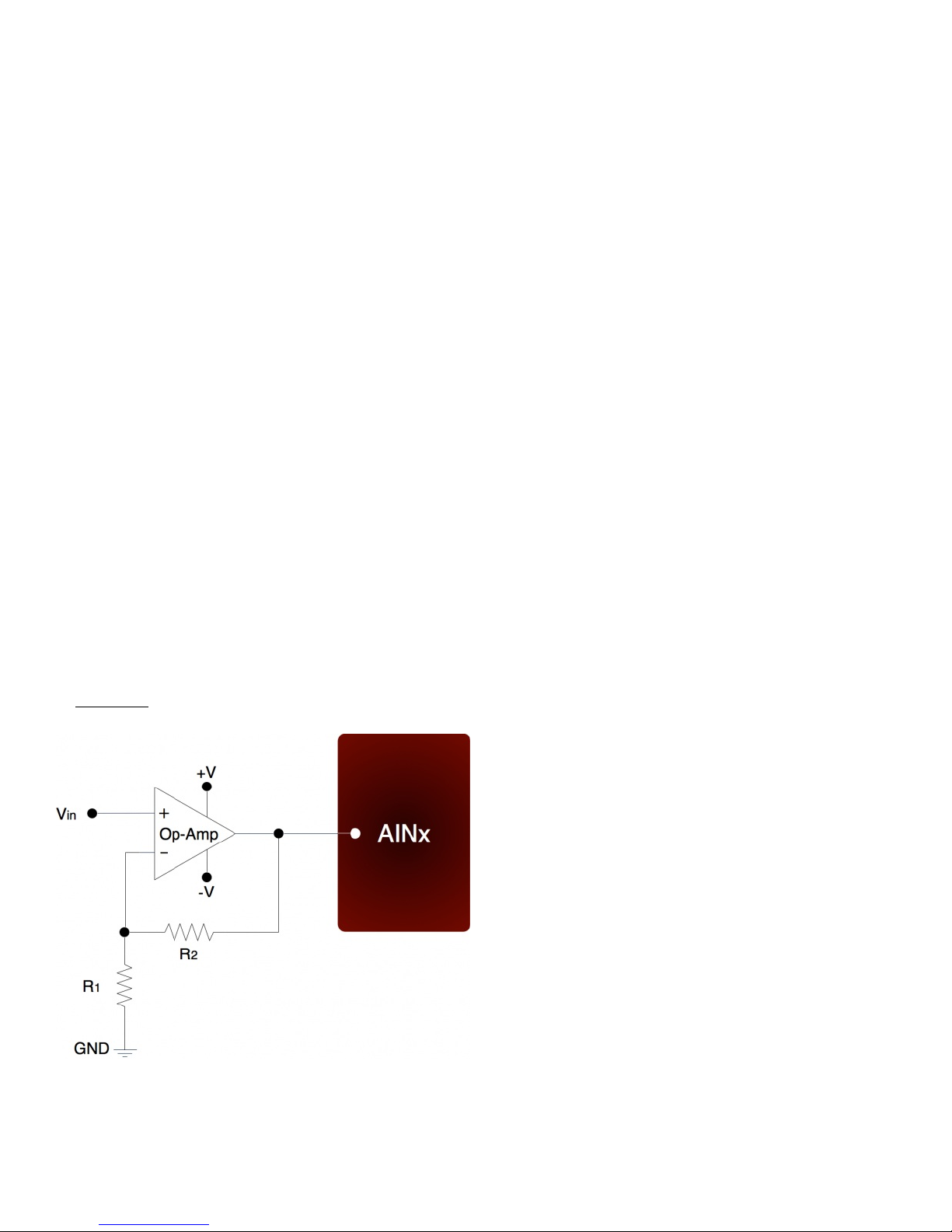
2.7.3.5 - Amplifying Small Signal Voltages
The best results are generally obtained when a signal voltage spans the full analog input range of the LabJack. If the signal is too
small it can be amplified before connecting to the LabJack. One good way to handle low-level signals such as thermocouples is
the LJTick-InAmp, which is a 2-channel instrumentation amplifier module that plugs into the UE9 screw-terminals.
For a do-it-yourself solution, the following figure shows an operational amplifier (op-amp) configured as non-inverting:
Figure 2-3. Non-Inverting Op-Amp Configuration
The gain of this configuration is:
Vout = Vin * (1 + (R2/R1))
100 kΩ is a typical value for R2. Note that if R2=0 (short-circuit) and R1=inf (not installed), a simple buffer with a gain equal to 1 is
the result.
11
Page 12
There are numerous criteria used to choose an op-amp from the thousands that are available. One of the main criteria is that the
op-amp can handle the input and output signal range. Often, a single-supply rail-to-rail input and output (RIRO) is used as it can be
powered from Vs and GND and pass signals within the range 0-Vs. The OPA344 from Texas Instruments (ti.com) is good for many
5 volt applications. The max supply rating for the OPA344 is 5.5 volts, so for applications using Vm+/Vm- (~12 volts) or using the
±10 volt supply on the EB37, the LT1490A from Linear Technologies (linear.com) might be a good option.
The op-amp is used to amplify (and buffer) a signal that is referred to the same ground as the LabJack (single-ended). If instead
the signal is differential (i.e. there is a positive and negative signal both of which are different than ground), an instrumentation
amplifier (in-amp) should be used. An in-amp converts a differential signal to single-ended, and generally has a simple method to
set gain.
The EB37 experiment board is handy for building these circuits.
2.7.3.6 - Signal Voltages Beyond ±5 Volts (and Resistance
Measurement)
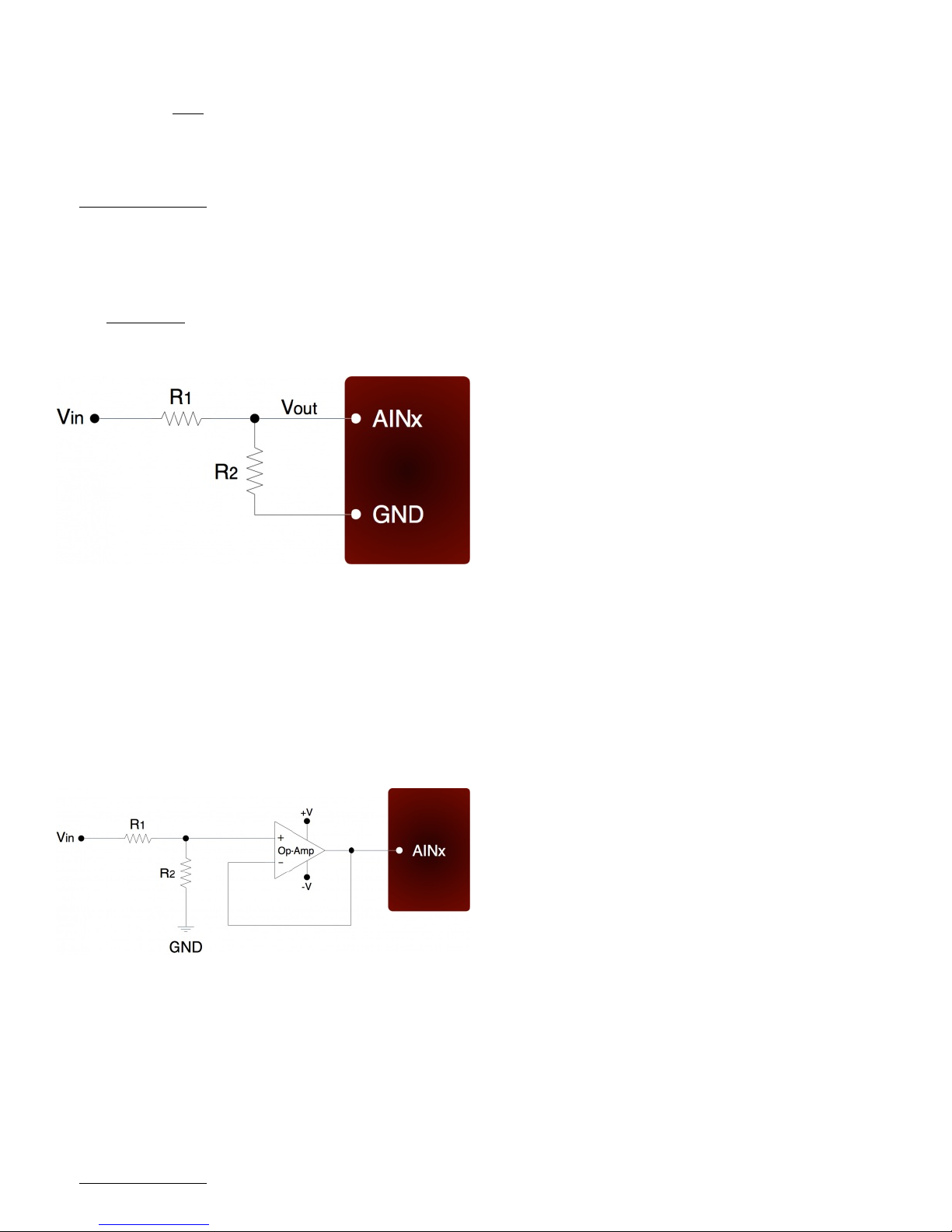
The nominal maximum analog input voltage range for the UE9 is ±5 volts. The easiest way to handle larger voltages is often by
using the LJTick-Divider, which is a two channel buffered divider module that plugs into the UE9 screw-terminals.
The basic way to handle higher voltages is with a resistive voltage divider. The following figure shows the resistive voltage divider
assuming that the source voltage (Vin) is referred to the same ground as the UE9 (GND).
Figure 2-4. Voltage Divider Circuit
The attenuation of this circuit is determined by the equation:
Vout = Vin * ( R2 / (R1+R2))
This divider is easily implemented by putting a resistor (R1) in series with the signal wire, and placing a second resistor (R2) from
the AIN terminal to a GND terminal. To maintain specified analog input performance, R1 should not exceed 10 kΩ, so R1 can
generally be fixed at 10 kΩ and R2 can be adjusted for the desired attenuation. For instance, R1 = R2 = 10 kΩ provides a divide
by 2, so a ±10 volt input will be scaled to ±5 volts and a 0-10 volt input will be scaled to 0-5 volts.
The divide by 2 configuration where R1 = R2 = 10 kΩ, presents a 20 kΩ load to the source, meaning that a ±10 volt signal will have
to be able to source/sink up to ±500 µA. Some signal sources might require a load with higher resistance, in which case a buffer
should be used. The following figure shows a resistive voltage divider followed by an op-amp configured as non-inverting unitygain (i.e. a buffer).
Figure 2-5. Buffered Voltage Divider Circuit
The op-amp is chosen to have low input bias currents so that large resistors can be used in the voltage divider. The LT1490A from
Linear Technologies (linear.com) is a good choice for dual-supply applications. The LT1490A only draws 40 µA of supply current,
thus many of these amps can be powered from the Vm+/Vm- supply on the UE9, and can pass signals in the ±5 volt range. Since
the input bias current is only -1 nA, large divider resistors such as R1 = R2 = 470 kΩ will only cause an offset of about -470 µV, and
yet present a load to the source of about 1 megaohm.
For 0-5 volt applications, where the amp will be powered from Vs and GND, the LT1490A is not the best choice. When the
amplifier input voltage is within 800 mV of the positive supply, the bias current jumps from -1 nA to +25 nA, which with R1 = 470 kΩ
will cause the offset to change from -470 µV to +12 mV. A better choice in this case would be the OPA344 from Texas Instruments
(ti.com). The OPA344 has a very small bias current that changes little across the entire voltage range. Note that when powering the
amp from Vs and GND, the input and output to the op-amp is limited to that range, so if Vs is 4.8 volts your signal range will be 0-
4.8 volts. If this is a concern, use the external wall-wart to supply power to the UE9 as it typically keeps Vs around 5.2 volts.
The EB37 experiment board is handy for building these circuits.
12
Page 13

The information above also applies to resistance measurement. A common way to measure resistance is to build a voltage
divider as shown in Figure 2-4, where one of the resistors is known and the other is the unknown. If Vin is known and Vout is
measured, the voltage divider equation can be rearranged to solve for the unknown resistance.
2.7.3.7 - Measuring Current (Including 4-20 mA) with a
Resistive Shunt
The best way to handle 4-20 mA signals is with the LJTick-CurrentShunt, which is a two channel active current to voltage converter
module that plugs into the UE9 screw-terminals.
The following figure shows a typical method to measure the current through a load, or to measure the 4-20 mA signal produced by
a 2-wire (loop-powered) current loop sensor. The current shunt shown in the figure is simply a resistor.
Figure 2-6. Current Measurement With Arbitrary Load or 2-Wire 4-20 mA Sensor
When measuring a 4-20 mA signal, a typical value for the shunt would be 240 Ω. This results in a 0.96 to 4.80 volt signal
corresponding to 4-20 mA. The external supply must provide enough voltage for the sensor and the shunt, so if the sensor requires
5 volts the supply must provide at least 9.8 volts.
For applications besides 4-20 mA, the shunt is chosen based on the maximum current and how much voltage drop can be
tolerated across the shunt. For instance, if the maximum current is 1.0 amp, and 2.5 volts of drop is the most that can be tolerated
without affecting the load, a 2.4 Ω resistor could be used. That equates to 2.4 watts, though, which would require a special high
wattage resistor. A better solution would be to use a 0.1 Ω shunt, and then use an amplifier to increase the small voltage produced
by that shunt. If the maximum current to measure is too high (e.g. 100 amps), it will be difficult to find a small enough resistor and a
hall-effect sensor should be considered instead of a shunt.
The following figure shows typical connections for a 3-wire 4-20 mA sensor. A typical value for the shunt would be 240 Ω which
results in 0.96 to 4.80 volts.
Figure 2-7. Current Measurement With 3-Wire 4-20 mA (Sourcing) Sensor
The sensor shown in Figure 2-7 is a sourcing type, where the signal sources the 4-20 mA current which is then sent through the
shunt resistor and sunk into ground. Another type of 3-wire sensor is the sinking type, where the 4-20 mA current is sourced from
the positive supply, sent through the shunt resistor, and then sunk into the signal wire. If sensor ground is connected to UE9 ground,
the sinking type of sensor presents a couple of problems, as the voltage across the shunt resistor is differential (neither side is at
ground) and at least one side of the resistor has a high common mode voltage (equal to the positive sensor supply). If the sensor
and/or UE9 are isolated, a possible solution is to connect the sensor signal or positive sensor supply to UE9 ground (instead of
sensor ground). This requires a good understanding of grounding and isolation in the system. The LJTick-CurrentShunt is often a
simple solution.
Both Figure 2-6 and 2-7 show a 0-100 Ω resistor in series with SGND, which is discussed in general in Section 2.7.3.4. In this
case, if SGND is used (rather than GND), a direct connection (0 Ω) should be good.
The best way to handle 4-20 mA signals is with the LJTick-CurrentShunt, which is a two channel active current to voltage converter
module that plugs into the UE9 screw-terminals.
2.7.3.8 - Floating/Unconnected Inputs
The reading from a floating (no external connection) analog input channel can be tough to predict and is likely to vary with sample
timing and adjacent sampled channels. Keep in mind that a floating channel is not at 0 volts, but rather is at an undefined voltage.
In order to see 0 volts, a 0 volt signal (such as GND) should be connected to the input.
Some data acquisition devices use a resistor, from the input to ground, to bias an unconnected input to read 0. This is often just
for “cosmetic” reasons so that the input reads close to 0 with floating inputs, and a reason not to do that is that this resistor can
degrade the input impedance of the analog input.
13
Page 14

In a situation where it is desired that a floating channel read a particular voltage, say to detect a broken wire, a resistor can be
placed from the AINx screw terminal to the desired voltage (GND, VS, DACx, …). A 10 kΩ resistor will pull the analog input
readings to within 1 binary count of any desired voltage, but obviously degrades the input impedance to 10 kΩ. For the specific
case of pulling a floating channel to 0 volts, a 100 kΩ resistor to GND can typically be used to provide analog input readings within
100 mV of ground.
2.7.4 - Internal Temperature Sensor
The UE9 has an internal temperature sensor. Although this sensor measures the temperature inside the UE9, it has been
calibrated to read ambient temperature. For accurate measurements the temperature of the entire UE9 must stabilize relative to
the ambient temperature, which can take on the order of 1 hour. Best results will be obtained in still air in an environment with
slowly changing ambient temperatures.
The internal temperature sensor is also affected by the operating speed of the UE9. With Control firmware V1.08 or higher, the
UE9 is in high power mode by default, which is assumed by the LabJack UD driver.
With the UD driver, the internal temperature sensor is read by acquiring analog input channel 133 or 141, and returns degrees K.
2.8 - DAC
There are two DACs (digital-to-analog converters or analog outputs) on the UE9. Each DAC can be set to a voltage between
about 0.02 and 4.86 volts with 12-bits of resolution.
Although the DAC values are based on an absolute reference voltage, and not the supply voltage, the DAC output buffers are
powered internally by Vs and thus the maximum output is limited to slightly less than Vs. Another implication of this is that high
frequency power supply noise might couple to the analog outputs.
The analog output commands are sent as raw binary values (low level functions). For a desired output voltage, the binary value can
be approximated as:
Bits(uncalibrated) = (Volts/4.86)*4096
For a proper calculation, though, use the calibration values (Slope and Offset) stored in the internal flash on the Control processor
(Table 2-4):
Bits = (Slope * Volts) + Offset
The DACs appear both on the screw terminals and on the DB37 connector. These connections are electrically the same, and the
user must exercise caution only to use one connection or the other, and not create a short circuit.
The DACS on the UE9 can be disabled. Prior to control firmware 1.98 when disabled they are placed in a high-impedance state,
firmware 1.98 and later always leaves the DACs enabled. Both DACs are enabled or disabled at the same time, so if a command
causes one DAC to be enabled the other is also enabled.
The power-up condition of the DACs can be configured by the user. From the factory, the DACS default to enabled at minimum
voltage (~0 volts). Note that even if the power-up default for a line is changed to a different voltage or disabled, there is a delay of
about 100 ms at power-up where the D ACs are in the factory default condition.
The analog outputs can withstand a continuous short-circuit to ground, even when set at maximum output.
Voltage should never be applied to the analog outputs, as they are voltage sources themselves. In the event that a voltage is
accidentally applied to either analog output, they do have protection against transient events such as ESD (electrostatic
discharge) and continuous overvoltage (or undervoltage) of a few volts.
There is an accessory available from LabJack called the LJTick-DAC that provides a pair of 14-bit analog outputs with a range of
±10 volts. The LJTick-DAC plugs into any digital I/O block, and thus up to 10 of these can be used per UE9 to add 20 analog
outputs.
2.8.1 - Typical Analog Output Connections
2.8.1 - Typical Analog Output Connections
The DACs on the UE9 can output quite a bit of current, but have 50 Ω of source impedance that will cause voltage drop. To avoid
this voltage drop, an op-amp can be used to buffer the output, such as the non-inverting configuration shown in Figure 2-3. A
simple RC filter can be added between the DAC output and the amp input for further noise reduction. Note that the ability of the
amp to source/sink current near the power rails must still be considered. A possible op-amp choice would be the TLV246x family
(ti.com).
2.8.1.2 - Different Output Ranges
There is an accessory available from LabJack called the LJTick-DAC that provides a pair of 14-bit analog outputs with a range of
±10 volts. The LJTick-DAC plugs into any digital I/O block, and thus up to 10 of these can be used per UE9 to add 20 analog
outputs.
The typical output range of the DACs is about 0.02 to 4.86 volts. For other unipolar ranges, an op-amp in the non-inverting
configuration (Figure 2-3) can be used to provide the desired gain. For example, to increase the maximum output from 4.86 volts
to 10.0 volts, a gain of 2.06 is required. If R2 (in Figure 2-3) is chosen as 100 kΩ, then an R1 of 93.1 kΩ is the closest 1% resistor
14
Page 15
that provides a gain greater than 2.06. The +V supply for the op-amp would have to be greater than 10 volts.
For bipolar output ranges, such as ±10 volts, a similar op-amp circuit can be used to provide gain and offset, but of course the opamp must be powered with supplies greater than the desired output range (depending on the ability of the op-amp to drive it’s
outputs close to the power rails). For example, the EB37 experiment board provides power supplies that are typically ±9.5 volts. If
these supplies are used to power the LT1490A op-amp (linear.com), which has rail-to-rail capabilities, the outputs could be driven
very close to ±9.5 volts. If ±12 or ±15 volt supplies are available, then the op-amp might not need rail-to-rail capabilities to achieve
the desired output range.
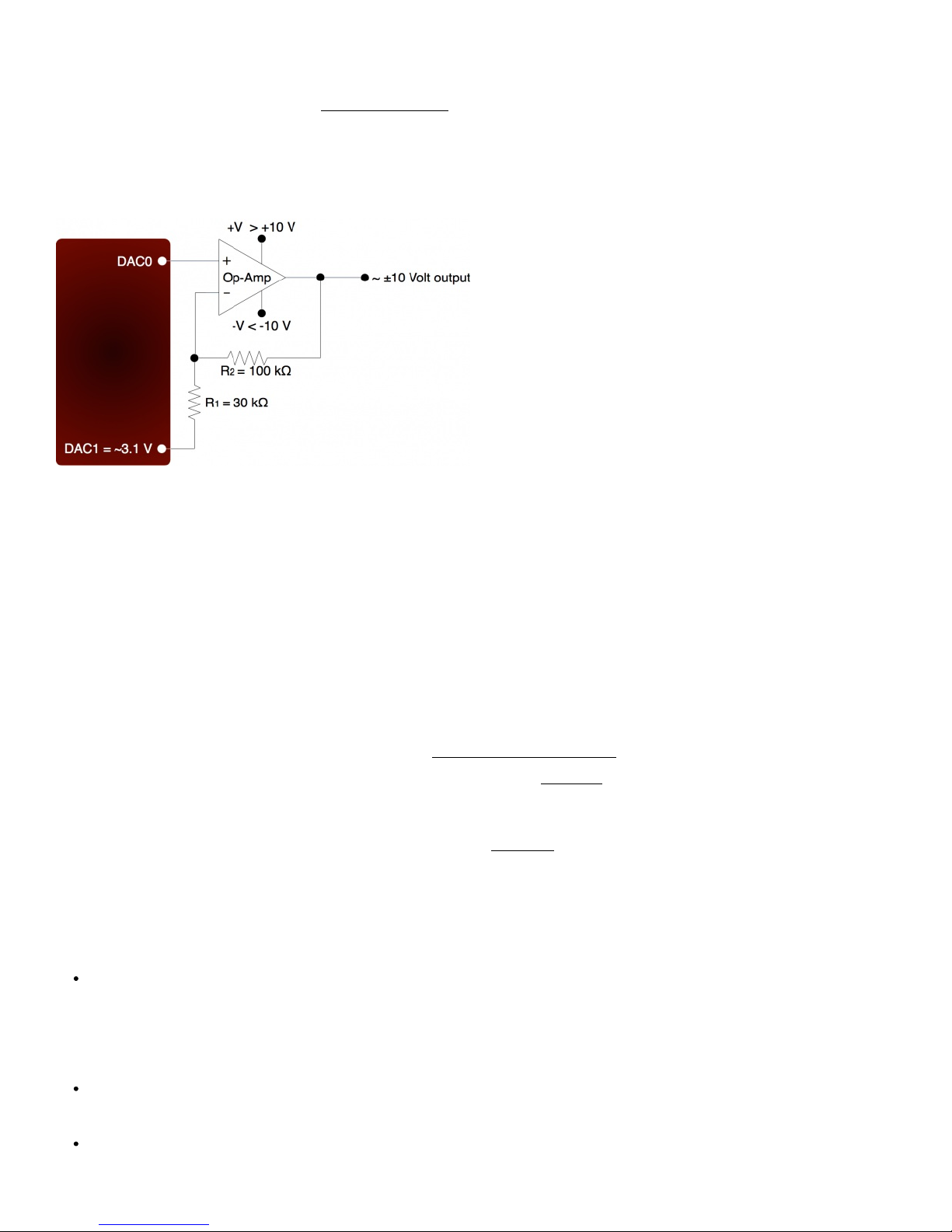
A reference voltage is also required to provide the offset. In the following circuit, DAC1 is used to provide a reference voltage. The
actual value of DAC1 can be adjusted such that the circuit output is 0 volts at the DAC0 mid-scale voltage, and the value of R1 can
be adjusted to get the desired gain. A fixed reference (such as 2.5 volts) could also be used instead of DAC1.
Figure 2-8. ±10 Volt DAC Output Circuit
A two-point calibration should be done to determine the exact input/output relationship of this circuit. Refer to application note
SLOA097 from ti.com for further information about gain and offset design with op-amps.
2.9 - Digital I/O
The LabJack UE9 has 23 digital I/O. The LabJackUD driver uses the following bit numbers to specify all the digital lines:
0-7 FIO0-FIO7
8-15 EIO0-EIO7
16-19 CIO0-CIO3
20-22 MIO0-MIO2
The UE9 has 8 FIO (flexible digital I/O). The first 4 lines, FIO0-FIO3, appear both on the screw terminals and on the DB37
connector. These connections are electrically the same, and the user must exercise caution only to use one connection or the
other, and not create a short circuit. The upper 4 lines appear only on the DB37 connector. By default, the FIO lines are digital I/O,
but they can also be configured as up to 6 timers and 2 counters (see Timers/Counters Section of this User’s Guide).
The 8 EIO and 4 CIO lines appear only on the DB15 connector. See the DB15 Section of this User’s Guide for more information.
MIO are standard digital I/O that also have a special multiplexer control function described in Section 2.7 above (AIN). The MIO are
addressed as digital I/O bits 20-22 by the Windows driver. The MIO hardware (electrical specifications) is the same as the
EIO/CIO hardware.
All the digital I/O include an internal series resistor that provides overvoltage/short-circuit protection. These series resistors also
limit the ability of these lines to sink or source current. Refer to the specifications in Appendix A .
All digital I/O on the UE9 have 3 possible states: input, output-high, or output-low. Each bit of I/O can be configured individually.
When configured as an input, a bit has a ~100 kΩ pull-up resistor to 3.3 volts (all digital I/O are 5 volt tolerant). When configured as
output-high, a bit is connected to the internal 3.3 volt supply (through a series resistor). When configured as output-low, a bit is
connected to GND (through a series resistor).
The fact that the digital I/O are specified as 5-volt tolerant means that 5 volts can be connected to a digital input without problems
(see the actual limits in the specifications in Appendix A). If 5 volts is needed from a digital output, consider the following solutions:
In some cases, an open-collector style output can be used to get a 5V signal. To get a low set the line to output-low, and to
get a high set the line to input. When the line is set to input, the voltage on the line is determined by a pull-up resistor. The
UE9 has an internal ~100k resistor to 3.3V, but an external resistor can be added to a different voltage. Whether this will
work depends on how much current the load is going to draw and what the required logic thresholds are. Say for example a
10k resistor is added from EIO0 to VS. EIO0 has an internal 100k pull-up to 3.3 volts and a series output resistance of about
180 ohms. Assume the load draws just a few microamps or less and thus is negligible. When EIO0 is set to input, there will
be 100k to 3.3 volts in parallel with 10k to 5 volts, and thus the line will sit at about 4.85 volts. When the line is set to outputlow, there will be 180 ohms in series with the 10k, so the line will be pulled down to about 0.1 volts.
The surefire way to get 5 volts from a digital output is to add a simple logic buffer IC that is powered by 5 volts and
recognizes 3.3 volts as a high input. Consider the CD74ACT541E from TI (or the inverting CD74ACT540E). All that is
needed is a few wires to bring VS, GND, and the signal from the LabJack to the chip. This chip can level shift up to eight
0/3.3 volt signals to 0/5 volt signals and provides high output drive current (+/-24 mA).
Note that the 2 DAC channels on the U3 can be set to 5 volts, providing 2 output lines with such capability.
15
Page 16
The power-up condition of the digital I/O can be configured by the user. From the factory, all digital I/O are configured to power-up
as inputs. Note that even if the power-up default for a line is changed to output-high or output-low, there is a delay of about 100 ms
at power-up where all digital I/O are in the factory default condition.
The low-level Feedback function (Section 5.3.3) writes and reads all digital I/O. See Section 3.1 for timing information. For
information about using the digital I/O under the Windows LabJackUD driver, see Section 4.3.5.
Many function parameters contain specific bits within a single integer parameter to write/read specific information. In particular,
most digital I/O parameters contain the information for each bit of I/O in one integer, where each bit of I/O corresponds to the same
bit in the parameter (e.g. the direction of FIO0 is set in bit 0 of parameter FIODir). For instance, in the function ControlConfig, the
parameter FIODir is a single byte (8 bits) that writes/reads the power-up direction of each of the 8 FIO lines:
if FIODir is 0, all FIO lines are input,
if FIODir is 1 (20), FIO0 is output, FIO1-FIO7 are input,
if FIODir is 5 (20 + 22), FIO0 and FIO2 are output, all other FIO lines are input,
if FIODir is 255 (20 + … + 27), FIO0-FIO7 are output.
2.9.1 - Typical Digital I/O Connections
2.9.1.1 - Input: Driven Signals
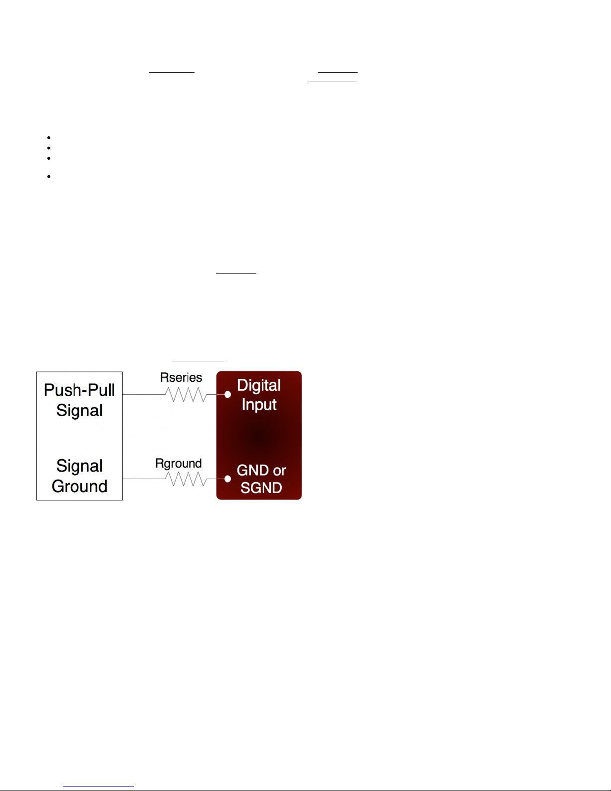
The most basic connection to a UE9 digital input is a driven signal, often called push-pull. With a push-pull signal the source is
typically providing a high voltage for logic high and zero volts for logic low. This signal is generally connected directly to the UE9
digital input, considering the voltage specifications in Appendix A. If the signal is over 5 volts, it can still be connected with a series
resistor. The digital inputs have protective devices that clamp the voltage at GND and VS, so the series resistor is used to limit the
current through these protective devices. For instance, if a 24 volt signal is connected through a 22 kΩ series resistor, about 19
volts will be dropped across the resistor, resulting in a current of about 0.9 mA, which is no problem for the UE9. The series
resistor should be 22 kΩ or less, to make sure the voltage on the I/O line when low is pulled below 1.0 volts.
The other possible consideration with the basic push-pull signal is the ground connection. If the signal is known to already have a
common ground with the UE9, then no additional ground connection is used. If the signal is known to not have a common ground
with the UE9, then the signal ground can simply be connected to UE9 GND. If there is uncertainty about the relationship between
signal ground and UE9 ground (e.g. possible common ground through AC mains), then a ground connection with a 100 Ω series
resistor is generally recommended (see Section 2.7.3.4).
Figure 2-9. Driven Signal Connection To Digital Input
Figure 2-9 shows typical connections. Rground is typically 0-100 Ω. Rseries is typically 0 Ω (short-circuit) for 3.3/5 volt logic, or 22
kΩ (max) for high-voltage logic. Note that an individual ground connection is often not needed for every signal. Any signals
powered by the same external supply, or otherwise referred to the same external ground, should share a single ground connection
to the UE9 if possible.
When dealing with a new sensor, a push-pull signal is often incorrectly assumed when in fact the sensor provides an open-collector
signal as described next.
2.9.1.2 - Input: Open-Collector Signals
Open-collector (also called open-drain or NPN) is a very common type of digital signal. Rather than providing 5 volts and ground,
like the push-pull signal, an open-collector signal provides ground and high-impedance. This type of signal can be thought of as a
switch connected to ground. Since the UE9 digital inputs have a 100 kΩ internal pull-up resistor, an open-collector signal can
generally be connected directly to the input. When the signal is inactive, it is not driving any voltage and the pull-up resistor pulls the
digital input to logic high. When the signal is active, it drives 0 volts which overpowers the pull-up and pulls the digital input to logic
low. Sometimes, an external pull-up (e.g. 4.7 kΩ from Vs to digital input) will be installed to increase the strength and speed of the
logic high condition.
16
Page 17
Figure 2-10. Open-Collector (NPN) Connection To Digital Input
Figure 2-10 shows typical connections. Rground is typically 0-100 Ω, Rseries is typically 0 Ω, and Rpullup, the external pull-up
resistor, is generally not required. If there is some uncertainty about whether the signal is really open-collector or could drive a
voltage beyond 5.8 volts, use an Rseries of 22 kΩ as discussed in Section 2.9.1.1, and the input should be compatible with an
open-collector signal or a driven signal up to at least 48 volts.
Without the optional resistors, the figure simplifies to:
Figure 2-10b. Simplified Open-Collector (NPN) Connection To Digital Input Without Optional Resistors
Note that an individual ground connection is often not needed for every signal. Any signals powered by the same external supply,
or otherwise referred to the same external ground, should share a single ground connection to the UE9 if possible.
2.9.1.3 - Input: Mechanical Switch Closure
To detect whether a mechanical switch (dry contact) is open or closed, connect one side of the switch to UE9 ground and the other
side to a digital input. The behavior is very similar to the open-collector described above.
Figure 2-11. Basic Mechanical Switch Connection To Digital Input
17
Page 18
When the switch is open, the internal 100 kΩ pull-up resistor will pull the digital input to about 3.3 volts (logic high). When the switch
is closed, the ground connection will overpower the pull-up resistor and pull the digital input to 0 volts (logic low). Since the
mechanical switch does not have any electrical connections, besides to the LabJack, it can safely be connected directly to GND,
without using a series resistor or SGND.
When the mechanical switch is closed (and even perhaps when opened), it will bounce briefly and produce multiple electrical
edges rather than a single high/low transition. For many basic digital input applications, this is not a problem as the software can
simply poll the input a few times in succession to make sure the measured state is the steady state and not a bounce. For
applications using timers or counters, however, this usually is a problem. The hardware counters, for instance, are very fast and will
increment on all the bounces. Some solutions to this issue are:
Software Debounce: If it is known that a real closure cannot occur more than once per some interval, then software can be
used to limit the number of counts to that rate.
Firmware Debounce: See section 2.10.1 for information about timer mode 6.
Active Hardware Debounce: Integrated circuits are available to debounce switch signals. This is the most reliable hardware
solution. See the MAX6816 (maxim-ic.com) or EDE2008 (elabinc.com).
Passive Hardware Debounce: A combination of resistors and capacitors can be used to debounce a signal. This is not
foolproof, but works fine in most applications.
Figure 2-12. Passive Hardware Debounce
Figure 2-12 shows one possible configuration for passive hardware debounce. First, consider the case where the 1 kΩ resistor is
replaced by a short circuit. When the switch closes it immediately charges the capacitor and the digital input sees logic low, but
when the switch opens the capacitor slowly discharges through the 22 kΩ resistor with a time constant of 22 ms. By the time the
capacitor has discharged enough for the digital input to see logic high, the mechanical bouncing is done. The main purpose of the
1 kΩ resistor is to limit the current surge when the switch is close. 1 kΩ limits the maximum current to about 5 mA, but better results
might be obtained with smaller resistor values.
2.9.1.4 - Output: Controlling Relays
All the digital I/O lines have series resistance that restricts the amount of current they can sink or source, but solid-state relays
(SSRs) can usually be controlled directly by the digital I/O. The SSR is connected as shown in the following diagram, where VS (~5
volts) connects to the positive control input and the digital I/O line connects to the negative control input (sinking configuration).
Figure 2-13. Relay Connections (Sinking Control, High-Side Load Switching)
When the digital line is set to output-low, control current flows and the relay turns on. When the digital line is set to input, control
current does not flow and the relay turns off. When the digital line is set to output-high, some current flows, but whether the relay is
on or off depends on the specifications of a particular relay. It is recommended to only use output-low and input.
18
Page 19

For example, the Series 1 (D12/D24) or Series T (TD12/TD24) relays from Crydom specify a max turn-on of 3.0 volts, a min turnoff of 1.0 volts, and a nominal input impedance of 1500 Ω.
When the digital line is set to output-low, it is the equivalent of a ground connection with 180 Ω (EIO/CIO/MIO) or 550 Ω (FIO)
in series. When using an EIO/CIO/MIO line, the resulting voltage across the control inputs of the relay will be about
5*1500/(1500+180) = 4.5 volts (the other 0.5 volts is dropped across the internal resistance of the EIO/CIO/MIO line). With
an FIO line the voltage across the inputs of the relay will be about 5*1500/(1500+550) = 3.7 volts (the other 1.3 volts are
dropped across the internal resistance of the FIO line). Both of these are well above the 3.0 volt threshold for the relay, so it
will turn on.
When the digital line is set to input, it is the equivalent of a 3.3 volt connection with 100 kΩ in series. The resulting voltage
across the control inputs of the relay will be close to zero, as virtually all of the 1.7 volt difference (between VS and 3.3) is
dropped across the internal 100 kΩ resistance. This is well below the 1.0 volt threshold for the relay, so it will turn off.
When the digital line is set to output-high, it is the equivalent of a 3.3 volt connection with 180 Ω (EIO/CIO/MIO) or 550 Ω
(FIO) in series. When using an EIO/CIO/MIO line, the resulting voltage across the control inputs of the relay will be about
1.7*1500/(1500+180) = 1.5 volts. With an FIO line the voltage across the inputs of the relay will be about
1.7*1500/(1500+550) = 1.2 volts. Both of these in the 1.0-3.0 volt region that is not defined for these example relays, so the
resulting state is unknown.
Mechanical relays require more control current than SSRs, and cannot be controlled directly by the digital I/O on the UE9. To
control higher currents with the digital I/O, some sort of buffer is used. Some options are a discrete transistor (e.g. 2N2222), a
specific chip (e.g. ULN2003), or an op-amp.
Note that the UE9 DACs can source enough current to control almost any SSR and even some mechanical relays, and thus can be
a convenient way to control 1 or 2 relays.
The RB12 relay board is a useful accessory available from LabJack. This board connects to the DB15 connector on the UE9 and
accepts up to 12 industry standard I/O modules (designed for Opto22 G4 modules and similar).
Another accessory available from LabJack is the LJTick-RelayDriver. This is a two channel module that plugs into the UE9 screwterminals, and allows two digital lines to each hold off up to 50 volts and sink up to 200 mA. This allows control of virtually any solidstate or mechanical relay.
2.10 - Timers/Counters
The UE9 has 6 timers (Timer0-Timer5) and 2 counters (Counter0-Counter1). When any of these timers or counters are enabled,
they take over an FIO line in sequence (Timer0, Timer1, …, Timer5, Counter0, Counter1). If any one of the 8 timers/counters is
enabled, it will take over FIO0. If any 2 are enabled, they will take over FIO0 and FIO1. If all 8 are enabled, they will take over all 8
FIO lines. Some examples:
1 Timer enabled, Counter0 disabled, Counter1 disabled
FIO0=Timer0
1 Timer enabled, Counter0 disabled, Counter1 enabled
FIO0=Timer0
FIO1=Counter1
6 Timers enabled, Counter0 enabled, Counter1 enabled
FIO0-FIO5=Timer0-Timer5
FIO6=Counter0
FIO7=Counter1
Timers and counters can appear on various pins, but other I/O lines never move. For example, Counter1 can appear anywhere
from FIO0 to FIO7, depending on how many timers are enabled and whether Counter0 is enabled.
Applicable digital I/O are automatically configured as input or output as needed when timers and counters are enabled, and stay
that way when the timers/counters are disabled.
See Section 2.9.1 for information about signal connections.
Each counter (Counter0 or Counter1) consists of a 32-bit register that accumulates the number of falling edges detected on the
external pin. If a counter is reset and read in the same function call, the read returns the value just before the reset.
Counter1 is used internally by stream mode, but in such a case only uses an FIO line if clock output or external triggering is used. If
any timers/counters are being used while starting/stopping a stream, the possible interaction between timer/counter configuration
and starting/stopping a stream needs to be considered.
The timers (Timer0-Timer5) have various modes available:
19
Page 20

Timer Modes
0
16-bit PWM output
1
8-bit PW M output
2
Period input (32-bit, rising edges)
3
Period input (32-bit, falling edges)
4
Duty cycle input
5
Firmware counter input
6
Firmware counter input (with debounce)
7
Frequency output
8
Quadrature input
9
Timer stop input (odd timers only)
10
System timer low read
11
System timer hight read
12
Period input (16-bit, rising edges)
13
Period input (16-bit, falling edges)
Table 2.10-1. UE9 Timer Modes
TimerClockBase
0
750 kHz
1
48 MHz (Sy stem)
Table 2.10-2. UE9 Timer Clock Options
All timers use the same timer clock (which affects modes 0, 1, 2, 3, 4, 7, 12, and 13). The timer clock is determined by dividing the
base clock by the clock divisor. The divisor has a range of 0-255, where 0 corresponds to a division of 256. There are 2 choices
for the timer base clock.
The low level TimerCounter function has a bit called UpdateConfig that must be set to change the timer clock, timer modes, or
number of timers/counters enabled. When this bit is set, all timers and counters are re-initialized. The LabJackUD driver
automatically sets this bit if any write requests are executed related to mode, enabling/disabling, or clock configuration.
The low level TimerCounter function has UpdateReset bits for each timer that must be set to change the timer value. The
LabJackUD driver automatically sets the appropriate bit when a value write is executed.
The low level TimerCounter function has Reset bits for each counter that must be set to reset the counter to zero. The LabJackUD
automatically sets the appropriate bit when a reset request is executed.
2.10.1 - Timer Mode Descriptions
2.10.1.1 - PWM Output (16-Bit, Mode 0)
Outputs a pulse width modulated rectangular wave output. Value passed should be 0-65535, and determines what portion of the
total time is spent low (out of 65536 total increments). That means the duty cycle can be varied from 100% (0 out of 65536 are low)
to 0.0015% (65535 out of 65536 are low).
The overall frequency of the PWM output is the clock frequency specified by TimerClockBase/TimerClockDivisor divided by 216.
The following table shows the range of available PWM frequencies based on timer clock settings.
PWM16 Frequency
Ranges
TimerClockBase
Divisor=1
Divisor=256
0
750 kHz
11.44
0.04
750000
1
48 MHz (Sy stem)
732.42
2.86
48000000
Table 2.10.1.1-1. 16-bit PW M Fre quency Ranges
The same clock applies to all timers, so all 16-bit PWM channels will have the same frequency and will have their falling edges at
the same time.
PWM output starts by setting the digital line to output-low for the specified amount of time. The output does not necessarily start
instantly, but rather waits for the internal clock to roll. For example, if the PWM frequency is 100 Hz, that means the period is 10
milliseconds, and thus after the command is received by the device it could be anywhere from 0 to 10 milliseconds before the start
of the PWM output.
If a duty cycle of 0.0% (totally off) is required, consider using a simple inverter IC such as the CD74ACT540E from TI.
2.10.1.2 - PWM Output (8-Bit, Mode 1)
Outputs a pulse width modulated rectangular wave output. Value passed should be 0-65535, and determines what portion of the
total time is spent low (out of 65536 total increments). The lower byte is actually ignored since this is 8-bit PWM. That means the
duty cycle can be varied from 100% (0 out of 65536 are low) to 0.4% (65280 out of 65536 are low).
The overall frequency of the PWM output is the clock frequency specified by TimerClockBase/TimerClockDivisor divided by 28.
20
Page 21

The following table shows the range of available PWM frequencies based on timer clock settings.
PWM8 Frequency Ranges
TimerClockBase
Divisor=1
Divisor=256
0
750 kHz
2929.69
11.44
750000
1
48 MHz (Sy stem)
187500
732.42
48000000
Table 2.10.1.2-1. 8-bit PW M Fre quency Ranges
The same clock applies to all timers, so all 8-bit PWM channels will have the same frequency and will have their falling edges at
the same time.
PWM output starts by setting the digital line to output-low for the specified amount of time. The output does not necessarily start
instantly, but rather waits for the internal clock to roll. For example, if the PWM frequency is 100 Hz, that means the period is 10
milliseconds, and thus after the command is received by the device it could be anywhere from 0 to 10 milliseconds before the start
of the PWM output.
If a duty cycle of 0.0% (totally off) is required, consider using a simple inverter IC such as the CD74ACT540E from TI.
2.10.1.3 - Period Measurement (32-Bit, Modes 2 & 3)
Mode 2: On every rising edge seen by the external pin, this mode records the number of clock cycles (clock frequency determined
by TimerClockBase/TimerClockDivisor) between this rising edge and the previous rising edge. The value is updated on every
rising edge, so a read returns the time between the most recent pair of rising edges.
In this 32-bit mode, the Control processor must jump to an interrupt service routine to record the time, so small errors can occur if
another interrupt is already in progress. The possible error sources are:
Other edge interrupt timer modes (2/3/4/5/8/9/12/13). If an interrupt is already being handled due to an edge on another
timer, delays of a couple microseconds per timer are possible. That means if five other edge detecting timers are enabled, it
is possible (but not likely) to have about 10 microseconds of delay.
If a stream is in progress, every sample is acquired in a high-priority interrupt. These interrupts could cause delays of up to
10 microseconds.
The always active UE9 system timer causes an interrupt 11.4 times per second. If this interrupt happens to be in progress
when the edge occurs, a delay of about 1 microsecond is possible. If the software watchdog is enabled, the system timer
interrupt takes longer to execute and a delay of a few microseconds is possible.
Note that the minimum measurable period is limited by the edge rate limit discussed in Section 2.10.2.
Writing a value of zero to the timer performs a reset. After reset, a read of the timer value will return zero until a new edge is
detected. If a timer is reset and read in the same function call, the read returns the value just before the reset.
Mode 3 is the same except that falling edges are used instead of rising edges.
2.10.1.4 - Duty Cycle Measurement (Mode 4)
Records the high and low time of a signal on the external pin, which provides the duty cycle, pulse width, and period of the signal.
Returns 4 bytes, where the first two bytes (least significant word or LSW) are a 16-bit value representing the number of clock ticks
during the high signal, and the second two bytes (most significant word or MSW) are a 16-bit value representing the number of
clock ticks during the low signal. The clock frequency is determined by TimerClockBase/TimerClockDivisor.
The appropriate value is updated on every edge, so a read returns the most recent high/low times. Note that a duty cycle of 0% or
100% does not have any edges.
To select a clock frequency, consider the longest expected high or low time, and set the clock frequency such that the 16-bit
registers will not overflow.
Note that the minimum measurable high/low time is limited by the edge rate limit discussed in Section 2.10.2.
When using the LabJackUD driver the value returned is the entire 32-bit value. To determine the high and low time this value
should be split into a high and low word. One way to do this is to do a modulus divide by 216 to determine the LSW, and a normal
divide by 216 (keep the quotient and discard the remainder) to determine the MSW.
Writing a value of zero to the timer performs a reset. After reset, a read of the timer value will return zero until a new edge is
detected. If a timer is reset and read in the same function call, the read returns the value just before the reset. The duty cycle reset
is special, in that if the signal is low at the time of reset, the high-time/low-time registers are set to 0/65535, but if the signal is high
at the time of reset, the high-time/low-time registers are set to 65535/0. Thus if no edges occur before the next read, it is possible
to tell if the duty cycle is 0% or 100%.
2.10.1.5 - Firmware Counter Input (Mode 5)
On every rising edge seen by the external pin, this mode increments a 32-bit register. Unlike the pure hardware counters, these
timer counters require that the firmware jump to an interrupt service routine on each edge.
Writing a value of zero to the timer performs a reset. After reset, a read of the timer value will return zero until a new edge is
21
Page 22

detected. If a timer is reset and read in the same function call, the read returns the value just before the reset.
2.10.1.6 - Firmware Counter Input With Debounce (Mode 6)
Intended for frequencies less than 10 Hz, this mode adds a debounce feature to the firmware counter, which is particularly useful
for signals from mechanical switches. On every applicable edge seen by the external pin, this mode increments a 32-bit register.
Unlike the pure hardware counters, these timer counters require that the firmware jump to an interrupt service routine on each
edge.
When configuring only (UpdateConfig=1), the low byte of the timer value is a number from 0-255 that specifies a debounce period
in 87 ms increments (plus an extra 0-87 ms of variability):
Debounce Period = (0-87 ms) + (TimerValue * 87 ms)
In the high byte (bits 8-16) of the timer value, bit 0 determines whether negative edges (bit 0 clear) or positive edges (bit 0 set) are
counted.
Assume this mode is enabled with a value of 1, meaning that the debounce period is 87 ms and negative edges will be counted.
When the input detects a negative edge, it increments the count by 1, and then waits 87 ms before re-arming the edge detector.
Any negative edges within the 87 ms debounce period are ignored. This is good behavior for a normally-high signal where a
switch closure causes a brief low signal. The debounce period can be set long enough so that bouncing on both the switch closure
and switch open is ignored.
When only updating and not configuring, writing a value of zero to the timer performs a reset. After reset, a read of the timer value
will return zero until a new edge is detected. If a timer is reset and read in the same function call, the read returns the value just
before the reset.
2.10.1.7 - Frequency Output (Mode 7)
Outputs a square wave at a frequency determined by TimerClockBase/TimerClockDivisor divided by 2*Timer#Value. The Value
passed should be between 0-255, where 0 is a divisor of 256. By changing the clock configuration and timer value a wide range of
frequencies can be output. The maximum frequency is 48000000/2 = 24 MHz. The minimum frequency is (750000/256)/(2*256) =
5.7 Hz.
The frequency output has a -3 dB frequency of about 10 MHz on the FIO lines. Accordingly, at high frequencies the output
waveform will get less square and the amplitude will decrease.
The output does not necessarily start instantly, but rather waits for the internal clock to roll. For example, if the output frequency is
100 Hz, that means the period is 10 milliseconds, and thus after the command is received by the device it could be anywhere from
0 to 10 milliseconds before the start of the frequency output.
2.10.1.8 - Quadrature Input (Mode 8)
Requires 2 timer channels used in adjacent pairs (0/1, 2/3, or 4/5). Even timers will be quadrature channel A, and odd timers will
be quadrature channel B. The UE9 does 4x quadrature counting, and returns the current count as a signed 32-bit integer (2’s
complement). The same current count is returned on both even and odd timer value parameters.
Writing a value of zero to either or both timers performs a reset of both. After reset, a read of either timer value will return zero until
a new quadrature count is detected. If a timer is reset and read in the same function call, the read returns the value just before the
reset.
4X Counting
Quadrature mode uses the very common 4X counting method, which provides the highest resolution possible. That means you get
a count for every edge (rising & falling) on both phases (A & B). Thus if you have an encoder that provides 32 PPR, and you rotate
that encoder forward 1 turn, the timer Value register will be incremented by +128 counts.
Z-phase support
Quadrature mode supports Z-Phase. When enabled this feature will set the count to zero when the specified IO line sees a logic
high.
Z-phase is controlled by the value written to the timer during initialization. To enable z-phase support set bit 15 to 1 and set bits 0
through 4 to the DIO number that Z is connected to. EG: for a Z-line on EIO3 set the timer value to 0x800B or 32779. This value
should be sent to both the A and B timers.
Note that the LabJack will only check Z when it sees an edge on A or B.
Z-phase support requires Control Firmware 2.11 or later.
2.10.1.9 - Timer Stop Input (Mode 9)
This mode should only be assigned to odd numbered timers (1, 3, or 5). On every rising edge seen by the external pin, this
mode increments a 16-bit register. When that register matches the specified timer value (stop count value), the adjacent even
timer is stopped (0/1, 2/3, or 4/5). The range for the stop count value is 1-65535. Generally, the signal applied to this timer is from
the adjacent even timer, which is configured in some output timer mode. One place where this might be useful is for stepper
motors, allowing control over a certain number of steps.
Note that the timer is counting from the external pin like other input timer modes, so you must connect something to the stop timer
22
Page 23

input pin. For example, if you are using Timer1 to stop Timer0 which is outputting pulses, you must connect a jumper from Timer0
to Timer1.
Once this timer reaches the specified stop count value, and stops the adjacent timer, the timers must be reconfigured (set the
UpdateConfig bit for both timers, setting the UpdateConfig for just the output timer will restart the output in continuous mode) to
restart the adjacent timer, or the timer can be restarted by rewriting the value to the stop timer.
When the adjacent even timer is stopped, it is still enabled but just not outputting anything. Thus rather than returning to whatever
previous digital I/O state was on that terminal, it goes to the state “digital-input” (which has a 100 kΩ pull-up to 3.3 volts). That
means the best results are generally obtained if the terminal used by the adjacent even timer was initially configured as digital
input (factory default), rather than output-high or output-low. This will result in negative going pulses, so if you need positive going
pulses consider using a simple inverter IC such as the CD74ACT540E from TI.
The MSW of the read from this timer mode returns the number of edges counted, but does not increment past the stop count value.
The LSW of the read returns edges waiting for.
2.10.1.10 - System Timer Low/High Read (Modes 10 & 11)
The LabJack UE9 has a free-running internal 64-bit system timer with a frequency of 750 kHz. Timer modes 10 & 11 return the
lower or upper 32-bits of this timer. An FIO line is allocated for these modes like normal, even though they are internal readings
and do not require any external connections.
2.10.1.11 - Period Measurement (16-Bit, Modes 12 & 13)
Similar to the 32-bit edge-to-edge timing modes described above (modes 2 & 3), except that hardware capture registers are
used to record the edge times. This limits the times to 16-bit values, but is accurate to the resolution of the clock, and not subject to
any errors due to firmware processing delays.
Note that the minimum measurable period is limited by the edge rate limit discussed in Section 2.10.2.
2.10.2 - Timer Operation/Performance Notes
Note that the specified timer clock frequency is the same for all timers. That is, TimerClockBase and TimerClockDivisor are
singular values that apply to all timers. Modes 0, 1, 2, 3, 4, 7, 12, and 13, all are affected by the clock frequency, and thus the
simultaneous use of these modes has limited flexibility. This is often not an issue for modes 2 and 3 since they use 32-bit
registers.
The output timer modes (0, 1, and 7) are handled totally by hardware. Once started, no processing resources are used and other
UE9 operations do not affect the output. The major exception to this is if the TimerCounter UpdateConfig bit is set as described
earlier, as that will cause all output timers to stop and restart.
The edge-detecting timer input modes do require UE9 processing resources, as an interrupt is required to handle each edge.
Timer modes 2, 3, 5, 9, 12, and 13 must process every applicable edge (rising or falling). Timer modes 4 and 8 must process
every edge (rising and falling). To avoid missing counts, keep the total number of processed edges (all timers) less than 100,000
per second. That means that in the case of a single timer, there should be no more than 1 edge per 10 μs. For multiple timers, all
can process an edge simultaneously, but if for instance 6 timers get an edge at the same time, 60 μs should be allowed before any
further edges are applied. If streaming is occurring at the same time, the maximum edge rate will be less (25,000 per second),
and since each edge requires processing time the sustainable stream rates can also be reduced.
2.11 - SCL and SDA (or SCA)
Reserved for factory use. Note that the I²C functionality of the UE9 does not use these terminals.
2.12 - DB37
The DB37 connector brings out analog inputs, analog outputs, FIO, and other signals. Some signals appear on both the DB37
connector and screw terminals, so care must be taken to avoid a short circuit.
23
Page 24

DB37 Pinouts
1
GND14AIN927Vs
2
PIN2 (TX/ 200uA)
15
AIN728Vm+3FIO616AIN529DAC14FIO417AIN330GND5FIO218AIN131AIN126FIO019GND32AIN107MIO120PIN20 (RX/10uA)
33
AIN8
8
GND21FIO734AIN69Vm-22FIO535AIN4
10
GND23FIO336AIN2
11
DAC024FIO137AIN012AIN1325MIO0
13
AIN1126MIO2
Table 2.12-1. DB37 Connector Pinouts
Ground, Vs, AIN, DAC, FIO, and MIO are all described earlier.
Vm+/Vm- are bipolar power supplies intended to power external multiplexer ICs such as the MAX4051A (maxim-ic.com). The
multiplexers can only pass signals within their power supply range, so Vm+/Vm- can be used to pass bipolar signals. Nominal
voltage is ±5.8 volts at no load and ±5.6 volts at 1 mA. Both lines have a 100 ohm source impedance, and are designed to provide
1 mA or less. This is the same voltage supply used internally by the UE9 to bias the analog input amplifier and multiplexers. If this
supply is loaded more than 1 mA, the voltage can droop to the point that the maximum analog input range is reduced. If this supply
is severely overloaded (e.g. short circuited), then damage could eventually occur.
PIN2/PIN20 (TX0/RX0) currently bring out the UART transmit and receive lines, but in the future will likely be used as current
sources.
2.12.1 - CB37 Terminal Board
The CB37 terminal board from LabJack connects to the UE9’s DB37 connector and provides convenient screw terminal access to
all lines. The CB37 is designed to connect directly to the UE9, but can also connect via a 37-line 1:1 male-female cable.
When using the analog connections on the CB37, the effect of ground currents should be considered, particularly when a cable is
used and substantial current is sourced/sunk through the CB37 terminals. For instance, a test was done with a 6 foot cable
between the CB37 and UE9, and a 100 ohm load placed from Vs to GND on the CB37 (~50 mA load). A measurement of CB37
GND compared to UE9 GND showed 5.9 mV. If a signal was connected to AIN0 on the CB37 and referred to GND on the CB37,
the UE9 reading would be offset by 5.9 mV. The same test with the CB37 direct connected to the UE9 (no cable) resulted in an
offset of only 0.2 mV. In both cases (cable or no cable), the voltage measured between CB37 AGND and UE9 GND was 0.0 mV.
When any sizeable cable lengths are involved, a good practice is to separate current carrying ground from ADC reference ground.
An easy way to do this on the CB37 is to use GND as the current source/sink, and use AGND as the reference ground. This works
well for passive sensors (no power supply), such as a thermocouple, where the only ground current is the return of the input bias
current of the analog input.
2.12.2 - EB37 Experiment Board
The EB37 experiment board connects to the LabJack UE9’s DB37 connector and provides convenient screw terminal access.
Also provided is a solderless breadboard and useful power supplies. The EB37 is designed to connect directly to the LabJack,
but can also connect via a 37-line 1:1 male-female cable.
2.13 - DB15
The DB15 connector brings out 12 additional digital I/O. It has the potential to be used as an expansion bus, where the 8 EIO are
data lines and the 4 CIO are control lines.
In the Windows driver, the EIO are addressed as digital I/O bits 8 through 15, and the CIO are addressed as bits 16-19.
These 12 channels include an internal series resistor that provides overvoltage/short-circuit protection. These series resistors also
limit the ability of these lines to sink or source current. Refer to the specifications in Appendix A .
All digital I/O on the UE9 have 3 possible states: input, output-high, or output-low. Each bit of I/O can be configured individually.
When configured as an input, a bit has a ~100 kΩ pull-up resistor to 3.3 volts. When configured as output-high, a bit is connected
to the internal 3.3 volt supply (through a series resistor). When configured as output-low, a bit is connected to GND (through a
series resistor).
24
Page 25

DB15 Pinouts
1Vs9
CIO0
2
CIO110CIO23CIO311GND4EIO012EIO15EIO213EIO36EIO414EIO57EIO615EIO7
8
GND
Table 2.13-1. DB15 Connector Pinouts
2.13.1 - CB15 Terminal Board
The CB15 terminal board connects to the LabJack UE9’s DB15 connector. It provides convenient screw terminal access to the 12
digital I/O available on the DB15 connector. The CB15 is designed to connect directly to the LabJack, or can connect via a
standard 15-line 1:1 male-female DB15 cable.
2.13.2 - RB12 Relay Board
The RB12 relay board provides a convenient interface for the UE9 to industry standard digital I/O modules, allowing electricians,
engineers, and other qualified individuals, to interface a LabJack with high voltages/currents. The RB12 relay board connects to
the DB15 connector on the LabJack, using the 12 EIO/CIO lines to control up to 12 I/O modules. Output or input types of digital I/O
modules can be used. The RB12 is designed to accept G4 series digital I/O modules from Opto22, and compatible modules from
other manufacturers such as the G5 series from Grayhill. Output modules are available with voltage ratings up to 200 VDC or 280
VAC, and current ratings up to 3.5 amps.
2.14 - OEM Connector Options
As of this writing, the UE9 is only produced in the normal form factor with screw-terminals and DB connectors, but the PCB does
have alternate holes available for 0.1” pin-header installation.
Connectors J2 and J3 provide pin-header alternatives to the DB15 and DB37 connectors:
J2
1
GND2Vs3CIO04CIO1
5
CIO26CIO3
7
GND8EIO0
9
EIO110EIO211EIO312EIO4
13
EIO514EIO6
15
EIO716GND
Table 2.14-1. J2 OEM Pin-Heade rs
J3
1
GND2GND3PIN20
4
PIN25FIO76FIO67FIO58FIO49FIO3
10
FIO211FIO112FIO0
13
MIO014MIO115MIO2
16
GND17Vs18Vm-
19
Vm+20GND21DAC122DAC023GND24AIN13
25
AIN1226AIN1127AIN10
28
AIN929AIN830AIN731AIN632AIN533AIN424AIN335AIN236AIN137AIN038GND39GND
40
GND
Table 2.14-1. J3 OEM Pin-Heade rs
3 - Operation
The following sections discuss command/response mode and stream mode.
Command/response mode is where communication is initiated by a command from the host which is followed by a response from
the LabJack. Command/response is generally used at 1000 scans/second or slower and is generally simpler than stream
25
Page 26

mode.
Stream mode is a continuous hardware-timed input mode where a list of channels is scanned at a specified scan rate. The scan
rate specifies the interval between the beginning of each scan. The samples within each scan are acquired as fast as possible.
As samples are collected automatically by the LabJack, they are placed in a buffer on the LabJack, until retrieved by the host.
Stream mode is generally used at 10 scans/second or faster.
Command/response mode is generally best for minimum-latency applications such as feedback control. By latency here we
mean the time from when a reading is acquired to when it is available in the host software. A reading or group of readings can
be acquired in times on the order of a millisecond.
Stream mode is generally best for maximum-throughput applications where latency is not so important. Data is acquired very fast,
but to sustain the fast rates it must be buffered and moved from the LabJack to the host in large chunks. For example, a typical
stream application might set up the LabJack to acquire a single analog input at 50,000 samples/second. The LabJack moves this
data to the host in chunks of 25 samples each. The Windows UD driver moves data from the USB host memory to the UD driver
memory in chunks of 2000 samples. The user application might read data from the UD driver memory once a second in a chunk
of 50,000 samples. The computer has no problem retrieving, processing, and storing, 50k samples once per second, but it could
not do that with a single sample 50k times per second.
3.1 - Command/Response
Everything besides streaming is done in command/response mode, meaning that all communication is initiated by a command
from the host which is followed by a response from the UE9.
For everything besides timers and counters, the low-level Feedback function is the primary function used, as it writes and reads
virtually all I/O on the UE9. The Windows LabJackUD driver uses the Feedback function under-the-hood to handle most requests.
A single call to the Feedback function writes and reads all 23 digital I/O, updates the analog outputs, and reads up to 16 analog
inputs.
The following tables show typical measured execution times for the Feedback function. The time varies with the number of analog
inputs requested and the resolution of those inputs. These were measured by calling the function 1000 times and dividing the total
time by 1000, and thus include everything (Windows latency, communication time, UE9 processing time, etc.).
A “USB high-high” configuration means the UE9 is connected to a high-speed USB2 hub which is then connected to a high-speed
USB2 host. Even though the UE9 is not a high-speed USB device, such a configuration does provide improved performance.
Typical examples of “USB other” would be a UE9 connected to an old full-speed hub (hard to find) or more likely a UE9 connected
directly to the USB host (even if the host supports high-speed).
Resolution
Ethernet
USB high-high
USB other
Index
# AIN
[millis econds]
[millis econds]
[millis econds]
0
1.7
1.5
4
0-1241.9
1.7
4
0-1282.124
0-12162.7
2.4
4
1342
1.9
4
1382.4
2.3
4
13163.234.9
1442.7
2.5
4
1483.6
3.5
5
14165.6
5.8
6.3
1544.9
4.9
6
1588.2
8.1
9
1516151515
164141414
168272727
1616525252174525252178101
101
101
1716199
199
199
Table 3.1-1. Typical Feedback Function Execution Time s
Note that specifying a resolution index of 17, still returns 16-bit data, but is a special minimum noise mode.
As an example with the LabJackUD driver: If requests are added to write/read all 23 bits of digital I/O, update both analog outputs,
and read 16 12-bit analog inputs, the GoOne() function call can be expected to typically take about 2.6 ms to execute via Ethernet.
The AddRequest() and GetResult() calls take relatively no time at all.
A resolution value of 18 is passed to use the auxiliary high-resolution converter (24-bit sigma-delta) on the UE9-Pro. This is done
with the SingleIO low-level function, not the Feedback function. The UD driver will automatically use the SingleIO low-level function
when resolution is set to 18 on the UE9-Pro, and if there are requests for multiple samples the driver will make multiple SingleIO
calls.
26
Page 27

Resolution
Ethernet
USB high-high
USB other
Index
# AIN
[millis econds]
[millis econds]
[millis econds]
181125
125
125
(~125 ms per s ample)
Table 3.1-2. Typical Single IO Function Execution Time For Analog Input (UE9-Pro)
The low-level TimerCounter function is used to configure, update, reset, or read timer. When using the LabJackUD driver, any
timer/counter related requests will cause a call to the low-level TimerCounter function. The following tables show typical measured
execution times for the TimerCounter function. The execution time depends very little on what is being done and how many
timers/counters are being configured or read. These were measured by calling the function 1000 times and dividing the total time
by 1000, and thus include everything (Windows latency, communication time, UE9 processing time, etc.).
Ethernet
USB high-high
USB other
[millis econds]
[millis econds]
[millis econds]
TimerCounter
1.5
1.4
4
Table 3.1-3. Typical Time rCounter Function Execution Time s
3.2 - Stream Mode
The highest data rates are obtained in stream mode. Stream is a continuous hardware timed input mode where a list of channels
is scanned at a specified scan rate. The scan rate specifies the interval between the beginning of each scan. The samples within
each scan are acquired as fast as possible given the specified resolution and extra settling time if any.
As samples are collected, they are placed in a 4 Mbit FIFO buffer on the UE9, until retrieved by the host. This 4 Mbit buffer can
hold over 180,000 samples. Each data packet has various measures to ensure the integrity and completeness of the data
received by the host.
The table below shows the maximum streaming data rates for the UE9 versus analog input resolution (assumes no extra settling
time). These rates have been tested using Ethernet and various USB configurations, but some systems might require a USB highhigh configuration or Ethernet to obtain these speeds. A “USB high-high” configuration means the UE9 is connected to a highspeed USB2 hub which is then connected to a high-speed USB2 host. Even though the UE9 is not a high-speed USB device,
such a configuration does often provide improved performance. For all USB configurations, the worst case continuous stream rate
seen in testing is 30 ksamples/s.
Stream data rates over USB and Ethernet can also be limited by other factors such as speed of the PC and quality of the network.
General techniques for robust continuous streaming include increasing the priority of the stream process, and designing an
application to automatically restart the stream if needed.
Max Stream
Index
Resolution
Samples/s
0-121250000
131316000
14144000
151510001616
250
Table 3.2-1. Recommende d Ma xi mum Strea m Data Rate s
A sample is defined as a single conversion of a single channel, while a scan is defined as a single conversion of all channels
being acquired. That means that according to Table 3-4 the maximum scan rate for a stream of five 12-bit channels is 50k/5 = 10
kscans/second.
The time between each sample within each scan, without any extra settling time, is a little less than one over the max stream rate
specified in the above table.
The values in Table 3-4 are generally worst-case conservative values. This is particularly true for the 12-bit value. The following
table shows the actual measured limits for 12-bit streaming (Comm firmware V1.40, Control firmware V1.84), reflecting the fact
that stream mode is more efficient with more channels. Note again that Table 3-5 shows sample rates not scan rates. Divide by the
number of channels to determine the scan rate.
Max Stream
Max Stream
Samples/s
Samples/s
# Channels
USB high-high
Ethernet
1
57000
57000
2
66000
66000
4
68000
74000
8
68000
78000
16
68000
80000
Table 3.2-2. Actual Max imum Strea m Da ta Ra tes (Resolution=12)
When the limits in Table 3-5 are exceeded, an error will occur. Probably scan overlap or buffer overflow. The UE9 will not return bad
data, so these max data rates can be attempted, and either valid data will be collected or an error will occur.
27
Page 28

For information about streaming under Windows using the LabJackUD driver, see Section 4.3.7.
In general, a low-level (not using the LabJackUD driver) Ethernet stream is done as follows:
Open TCP connection on port number PORTA.
Call FlushBuffer.
Open TCP connection on port number PORTB.
Call StreamConfig on PORTA to set the scan rate and load the scan table (list of channels to be sampled each scan).
Call StreamStart on PORTA to start the stream.
The UE9 will begin sending StreamData packets to the host using PORTB.
Call StreamStop on PORTA to stop the stream.
3.2.1 - External Triggering
The internal scan clock normally initiates each scan in stream mode. Optionally, an external pulse (falling edge) on the Counter1
FIO line can initiate each scan. In the low level StreamConfig function, this is enabled by setting bit 6 of byte 9. In the LabJackUD
Windows driver this is controlled with the put_config special channel LJ_chSTR EAM_EXTERNAL_TRIGGER.
One application of external triggering is for synchronized streaming from multiple devices. In such a case, set bit 7 of byte 9 on the
main unit to enable scan pulse output. In the LabJackUD Windows driver this is controlled with the put_config special channel
LJ_chSTR EAM_CLOCK_OUTPUT. The main unit will then use the internal scan clock to initiate each scan, and output a pulse
per scan on the Counter1 FIO line. The output is normally high, goes low at the beginning of each scan, and stays low for about 6
microseconds. All other synchronized units are then configured for an external scan trigger.
Something that could be useful is the ability to define a scan with multiple samples from the same channel. So for instance, a scan
could be defined as channels 0/1/0/1/0/1 or 0/0/1/1 or whatever. This can provide a small burst of samples for each external
trigger. The scan list can have up to 128 channels. When using the LabJackUD driver, duplicate channels in a scan only works if
reading all channels simultaneously, as channel-by-channel stream reads are specified by channel number.
One thing to consider when using external triggering is the buffering that takes place within the UE9 and PC. If the external signal is
fairly continuous, such as in synchronized streaming, this is not a problem, but if the external trigger is more of a one-time pulse the
buffering must be considered to get the data when desired. For instance, each UE9 stream data packet contains 16 samples, so
if there is only 1 sample per scan the UE9 will not send any data until it has accumulated 16 scans. Some applications might
resolve this by defining each scan as 16 samples, even if it is just 16 samples of the same channel (see previous paragraph).
Another buffering issue will come into play if the LabJackUD driver is used with USB communication, as the driver reads 4
packets at a time (64 samples).
Streaming always uses Counter1 internally, and thus Counter1 is not available for counting while streaming. Additionally, if clock
output or external triggering is enabled, the normal Counter1 FIO line will be claimed, which is the next FIO available after all other
enabled timers/counters. If no other timers/counters are enabled, FIO0 will be used for stream clock output or input.
When using external stream clock output or input, the timer/counter configuration should not be changed after starting the stream,
as that could cause a glitch or could even cause the Counter1 FIO pin number to change.
Enabling clock output causes the FIO line to be set to output when the configuration command is executed, but the clock output will
not actually begin until the stream is started. Enabling clock input causes the FIO line to be set to input when the configuration
command is executed, but interrupts will not occur until the stream is started.
Note that external triggering causes 1 scan per trigger pulse. It is not used where a single pulse starts a continuous stream or a
burst of multiple scans, as that type of trigger is better handled in software. In software, an arbitrarily complex set of trigger
conditions can be watched for in continuous stream data, and when the trigger occurs the software can “keep” a specified number
of scans, “keep” all scans while the trigger is true, or whatever other behavior is desired. In addition, the software can maintain a
history buffer and “keep” a specified number of scans before the trigger (pre-trigger scans). Since stream data can consist of
analog, digital, and timer/counter inputs, the trigger conditions can use any or all of those.
3.2.2 - Streaming Digital Inputs, Timers, and Counter0
There are special channel numbers that allow digital inputs, timers, and Counter0, to be streamed in with analog input data.
Table 3-6. Spe cial Strea m
Channe ls
Channel#
193
EIO_FIO
194
MIO_CIO
200
Timer0
201
Timer1
202
Timer2
203
Timer3
204
Timer4
205
Timer5
210
Counter0
Channel number 193 returns the input states of 16 bits of digital I/O. FIO is the lower 8 bits and EIO is the upper 8 bits. This
channel is generally used to acquire digital input data in stream mode. Channel 194 is the same thing for the CIO and MIO lines
(Control firmware V1.69 or higher). The CIO are in the lower byte and the MIO are in the upper byte.
Channels 200-205 and 210 retrieve the least significant word (LSW, lower 2 bytes) of the specified timer/counter. At the same
time that any one of these is sampled, the most significant word (MSW, upper 2 bytes) of that particular timer/counter is stored in
an internal capture register (TC_Capture), so that the proper value can be sampled later in the scan. For any timer/counter where
the MSW is wanted, channel number 224 must be sampled after that channel and before any other timer/counter channel. For
28
Page 29

example, a scan list of {200,224,201,224} would get the LSW of Timer0, the MSW of Timer0, the LSW of Timer1, and the MSW of
Timer1. A scan list of {200,201,224} would get the LSW of Timer0, the LSW of Timer1, and the MSW of Timer1 (MSW of Timer0 is
lost).
Adding these special channels to the stream scan list does not configure those inputs. If any of the FIO or EIO lines have been
configured as outputs, they will need to be reconfigured as inputs to provide proper reads. The timers/counters must be configured
before streaming using normal timer/counter configuration commands.
The timing for these special channels is the same as for normal analog channels. For instance, a stream of the scan list
{0,1,200,224,201,224} counts as 6 channels, and the maximum scan rate is determined by taking the maximum sample rate at the
specified resolution and dividing by 6.
It is not recommended to stream timers configured in mode 2 or 3 (32-bit period measurement). It is possible for the LSW to roll,
but the MSW be captured before it is incremented. That means that only the LSW is reliable, and thus you might as well just use
the 16-bit modes.
Mode 11, the upper 32 bits of the system timer, is not available for stream reads. Note that when streaming with the internal scan
trigger, the timing is known anyway (elapsed time = scan rate * scan number) and it does not make sense to stream the system
timer modes 10 or 11. With external triggering, there might be reasons to stream the available timer mode 10.
4 - LabJackUD High-Level Driver
The low-level UE9 functions are described in Section 5, but most Windows applications will use the LabJackUD driver instead.
The latest version of the driver driver requires a PC running Windows XP or newer. The 3.07 version, supports Windows 98, ME,
2000. It is recommended to install the software before making a USB connection to a LabJack.
The download version of the installer consists of a single executable. This installer places the driver (LabJackUD.dll) in the
Windows System directory, along with a support DLL (LabJackUSB.dll). Generally this is c:\Windows\System\ on Windows 98/ME,
c:\Windows\System32\ on Windows 2000/XP, and c:\Windows\SysWOW64\ on newer 64-bit Windows.
Other files, including the header and Visual C library file, are installed to the LabJack drivers directory which defaults to c:\Program
Files\LabJack\drivers\.
4.1 - Overview
The general operation of the LabJackUD functions is as follows:
Open a LabJack.
Build a list of requests to perform (Add).
Execute the list (Go).
Read the result of each request (Get).
For example, to write an analog output and read an analog input:
//Use one of the following lines to op en the first found LabJack UE9
//over USB or Ethernet and get a handl e to the device.
//The general form of the open functio n is:
//Open LabJack (DeviceType, ConnectionT ype, Address, FirstFound, *Handl e)
//Open the first found LabJack UE9 ove r USB.
lngErr orcode = OpenLabJack (LJ_dtUE9, LJ_ctUSB, "1", 1, &lngHandle);
// … o r open a specified LabJack UE9 o ver Ethernet.
lngErr orcode = OpenLabJack (LJ_dtUE9, LJ_ctETHERNET, "192.168.1.209", 0, &lngHandle);
//Set DAC1 to 2.5 volts.
//The general form of the AddRequest f unction is:
//AddR equest (Handle, IOType, Channel, Value, x1, UserData)
lngErr orcode = AddRequest (lngHandle, LJ_ioPUT_DAC, 1, 2.50, 0, 0);
//Requ est a read from AIN3.
lngErr orcode = AddRequest (lngHandle, LJ_ioGET_AIN, 3, 0, 0, 0);
//Exec ute the requests.
lngErr orcode = GoOne (lngHandle);
//Get the result of the DAC1 request j ust to check for an errorcode.
//The general form of the GetResult fu nction is:
//GetR esult (Handle, IOType, Channel, *Value)
lngErr orcode = GetResult (lngHandle, L J_ioPUT_DAC, 1, 0);
//Get the AIN3 voltage.
lngErr orcode = GetResult (lngHandle, L J_ioGET_AIN, 3, &dblValue);
The AddRequest/Go/GetResult method is often the most efficient. As shown above, multiple requests can be executed with a
single Go() or GoOne() call, and the driver might be able to optimize the requests into fewer low-level calls. The other option is to
use the eGet or ePut functions which combine the AddRequest/Go/GetResult into one call. The above code would then look like
(assuming the UE9 is already open):
//Set DAC1 to 2.5 volts.
//The general form of the ePut functio n is:
//ePut (Handle, IOType, Channel, Value , x1)
lngErr orcode = ePut (lngHandle, LJ_ioP UT_DAC, 1, 2.50, 0);
//Read AIN3.
29
Page 30

//The general form of the eGet functio n is:
//eGet (Handle, IOType, Channel, *Valu e, x1)
lngErr orcode = eGet (lngHandle, LJ_ioG ET_AIN, 3, &dblValue, 0);
In the case of the UE9, the first example using add/go/get handles both the DAC command and AIN read in a single low-level call,
while in the second example using ePut/eGet two low-level commands are used. Examples in the following documentation will use
both the add/go/get method and the ePut/eGet method, and they are generally interchangeable. See Section 4.3 for more
pseudocode examples.
All the request and result functions always have 4 common parameters, and some of the functions have 2 extra parameters:
Handle – This is an input to all request/result functions that tells the function what LabJack it is talking to. The handle is
obtained from the OpenLabJack function.
IOType – This is an input to all request/result functions that specifies what type of action is being done.
Channel – This is an input to all request/result functions that generally specifies which channel of I/O is being written/read,
although with the config IOTypes special constants are passed for channel to specify what is being configured.
Value – This is an input or output to all request/result functions that is used to write or read the value for the item being
operated on.
x1 – This parameter is only used in some of the request/result functions, and is used when extra information is needed for
certain IOTypes.
UserData – This parameter is only used in some of the request/result functions, and is data that is simply passed along with
the request, and returned unmodified by the result. Can be used to store any sort of information with the request, to allow a
generic parser to determine what should be done when the results are received.
4.1.1 - Function Flexibility
The driver is designed to be flexible so that it can work with various different LabJacks with different capabilities. It is also
designed to work with different development platforms with different capabilities. For this reason, many of the functions are
repeated with different forms of parameters, although their internal functionality remains mostly the same. In this documentation, a
group of functions will often be referred to by their shortest name. For example, a reference to Add or AddRequest most likely
refers to any of the three variations: AddRequest(), AddRequestS() or AddRequestSS().
In the sample code, alternate functions (S or SS versions) can generally be substituted as desired, changing the parameter types
accordingly. All samples here are written in pseudo-C.
Functions with an “S” or “SS” appended are provided for programming languages that can’t include the LabJackUD.h file and
therefore can’t use the constants included. It is generally poor programming form to hardcode numbers into function calls, if for no
other reason than it is hard to read. Functions with a single “S” replace the IOType parameter with a const char * which is a string.
A string can then be passed with the name of the desired constant. Functions with a double “SS” replace both the IOType and
Channel with strings. OpenLabJackS replaces both DeviceType and ConnectionType with strings since both take constants.
For example:
In C, where the LabJackUD.h file can be included and the constants used directly:
AddReq uest(Handle, LJ_ioGET_CONFIG, LJ _chHARDWARE_VERSION,0,0,0);
The bad way (hard to read) when LabJackUD.h cannot be included:
AddReq uest(Handle, 1001, 10, 0, 0, 0);
The better way when LabJackUD.h cannot be included, is to pass strings:
AddReq uestSS(Handle, “LJ_ioGET_CONFIG” , “LJ_chHARDWARE_VERSION”,0,0,0) ;
Continuing on this vein, the function StringToConstant() is useful for error handling routines, or with the GetFirst/Next functions
which do not take strings. The StringToConstant() function takes a string and returns the numeric constant. So, for example:
LJ_ERR OR err;
err = AddRequestSS(Handle, “LJ_ioGETCO NFIG”, “LJ_chHARDWARE_VERSION”,0 ,0,0);
if (er r == StringToConstant(“LJE_INVAL ID_DEVICE_TYPE”))
do s ome error handling..
Once again, this is much clearer than:
if (er r == 2)
4.1.2 - Multi-Threaded Operation
This driver is completely thread safe. With some very minor exceptions, all these functions can be called from multiple threads at
the same time and the driver will keep everything straight. Because of this Add, Go, and Get must be called from the same thread
for a particular set of requests/results. Internally the list of requests and results are split by thread. This allows multiple threads to be
used to make requests without accidentally getting data from one thread into another. If requests are added, and then results return
LJE_NO_DATA_AVAILABLE or a similar error, chances are the requests and results are in different threads.
The driver tracks which thread a request is made in by the thread ID. If a thread is killed and then a new one is created, it is
possible for the new thread to have the same ID. Its not really a problem if Add is called first, but if Get is called on a new thread
results could be returned from the thread that already ended.
As mentioned, the list of requests and results is kept on a thread-by-thread basis. Since the driver cannot tell when a thread has
ended, the results are kept in memory for that thread regardless. This is not a problem in general as the driver will clean it all up
when unloaded. When it can be a problem is in situations where threads are created and destroyed continuously. This will result in
the slow consumption of memory as requests on old threads are left behind. Since each request only uses 44 bytes, and as
mentioned the ID’s will eventually get recycled, it will not be a huge memory loss. In general, even without this issue, it is strongly
30
Page 31

recommended to not create and destroy a lot of threads. It is terribly slow and inefficient. Use thread pools and other techniques to
keep new thread creation to a minimum. That is what is done internally.
The one big exception to the thread safety of this driver is in the use of the Windows TerminateThread() function. As is warned in
the MSDN documentation, using TerminateThread() will kill the thread without releasing any resources, and more importantly,
releasing any synchronization objects. If TerminateThread() is used on a thread that is currently in the middle of a call to this driver,
more than likely a synchronization object will be left open on the particular device and access to the device will be impossible until
the application is restarted. On some devices, it can be worse. On devices that have interprocess synchronization, such as the
U12, calling TerminateThread() may kill all access to the device through this driver no matter which process is using it and even if
the application is restarted. Avoid using TerminateThread()! All device calls have a timeout, which defaults to 1 second, but can be
changed. Make sure to wait at least as long as the timeout for the driver to finish.
4.2 - Function Reference
The LabJack driver file is named LabJackUD.dll, and contains the functions described in this section.
Some parameters are common to many functions:
LJ_ERROR – A LabJack specific numeric error code. 0 means no error. (long, signed 32-bit integer).
LJ_HANDLE – This value is returned by OpenLabJack, and then passed on to other functions to identify the opened
LabJack. (long, signed 32-bit integer).
To maintain compatibility with as many languages as possible, every attempt has been made to keep the parameter types very
basic. Also, many functions have multiple prototypes. The declarations that follow, are written in C.
To help those unfamiliar with strings in C, these functions expect null terminated 8 bit ASCII strings. How this translates to a
particular development environment is beyond the scope of this documentation. A const char * is a pointer to a string that won’t be
changed by the driver. Usually this means it can simply be a constant such as “this is a string”. A char * is a pointer to a string that
will be changed. Enough bytes must be preallocated to hold the possible strings that will be returned. Functions with char * in their
declaration will have the required length of the buffer documented below.
Pointers must be initialized in general, although null (0) can be passed for unused or unneeded values. The pointers for
GetStreamData and RawIn/RawOut requests are not optional. Arrays and char * type strings must be initialized to the proper size
before passing to the DLL.
4.2.1 - ListAll()
Returns all the devices found of a given DeviceType and ConnectionType. Searching over Ethernet relies on the DiscoveryUDP
function (Section 5.2.3), which might not work on certain network configurations.
ListAllS() is a special version where DeviceType and ConnectionType are strings rather than longs. This is useful for passing string
constants in languages that cannot include the header file. The strings should contain the constant name as indicated in the header
file (such as “LJ_dtUE9” and ”LJ_ctUSB”). The declaration for the S version of open is the same as below except for (const char
*pDeviceType, const char *pConnectionType, …).
Declaration:
LJ_ERR OR _stdcall ListAll ( long Devi ceType,
long Conn ectionType,
long *pNu mFound,
long *pSe rialNumbers,
long *pID s,
double *p Addresses)
Parameter Description:
Returns: LabJack errorcodes or 0 for no error.
Inputs:
DeviceType – The type of LabJack to search for. Constants are in the labjackud.h file.
ConnectionType – Enter the constant for the type of connection to use in the search.
pSerialNumbers – Must pass a pointer to a buffer with at least 128 elements.
pIDs – Must pass a pointer to a buffer with at least 128 elements.
pAddresses – Must pass a pointer to a buffer with at least 128 elements.
Outputs:
pNumFound – Returns the number of devices found, and thus the number of valid elements in the return arrays.
pSerialNumbers – Array contains serial numbers of any found devices.
pIDs – Array contains local IDs of any found devices.
pAddresses – Array contains IP addresses of any found devices. The function DoubleToStringAddress() is useful to convert
these to string notation.
4.2.2 - OpenLabJack()
Call OpenLabJack() before communicating with a device. This function can be called multiple times, however, once a LabJack is
open, it remains open until your application ends (or the DLL is unloaded). If OpenLabJack is called repeatedly with the same
parameters, thus requesting the same type of connection to the same LabJack, the driver will simply return the same LJ_HANDLE
every time. Internally, nothing else happens. This includes when the device is reset, or disconnected. Once the device is
reconnected, the driver will maintain the same handle. If an open call is made for USB, and then Ethernet, a different handle will be
returned for each connection type and both connections will be open.
31
Page 32

OpenLabJackS() is a special version of open where DeviceType and ConnectionType are strings rather than longs. This is useful
for passing string constants in languages that cannot include the header file. The strings should contain the constant name as
indicated in the header file (such as “LJ_dtUE9” and ”LJ_ctUSB”). The declaration for the S version of open is the same as below
except for (const char *pDeviceType, const char *pConnectionType, …).
Declaration:
LJ_ERR OR _stdcall OpenLabJack ( long DeviceType,
long ConnectionType,
const char *pAddress,
long FirstFound,
LJ_HA NDLE *pHandle)
Parameter Description:
Returns: LabJack errorcodes or 0 for no error.
Inputs:
DeviceType – The type of LabJack to open. Constants are in the labjackud.h file.
ConnectionType – Enter the constant for the type of connection, USB or Ethernet.
pAddress – For USB, pass the local ID or serial number of the desired LabJack. For Ethernet pass the IP address of the
desired LabJack. If FirstFound is true, Address is ignored.
FirstFound – If true, then the Address and ConnectionType parameters are ignored and the driver opens the first LabJack
found with the specified DeviceType. Generally only recommended when a single LabJack is connected. Currently only
supported with USB. If a USB device is not found, it will try Ethernet but with the given Address.
Outputs:
pHandle – A pointer to a handle for a LabJack.
4.2.3 - eGet() and ePut()
The eGet and ePut functions do AddRequest, Go, and GetResult, in one step.
The eGet versions are designed for inputs or retrieving parameters as they take a pointer to a double where the result is placed,
but can be used for outputs if pValue is preset to the desired value. This is also useful for things like StreamRead where a value is
input and output (number of scans requested and number of scans returned).
The ePut versions are designed for outputs or setting configuration parameters and will not return anything except the errorcode.
eGetS() and ePutS() are special versions of these functions where IOType is a string rather than a long. This is useful for passing
string constants in languages that cannot include the header file, and is generally used with all IOTypes except put/get config. The
string should contain the constant name as indicated in the header file (such as “LJ_ioANALOG_INPUT”). The declarations for the
S versions are the same as the normal versions except for (…, const char *pIOType, …).
eGetSS() and ePutSS() are special versions of these functions where IOType and Channel are strings rather than longs. This is
useful for passing string constants in languages that cannot include the header file, and is generally only used with the put/get
config IOTypes. The strings should contain the constant name as indicated in the header file (such as “LJ_ioPUT_CONFIG” and
“LJ_chLOCALID”). The declaration for the SS versions are the same as the normal versions except for (…, const char *pIOType,
const char *pChannel, …).
The declaration for ePut is the same as eGet except that Value is not a pointer (…, double Value, …), and thus is an input only.
Declaration:
LJ_ERR OR _stdcall eGet ( LJ_HANDLE Ha ndle,
long IOType,
long Channel ,
double *pVal ue,
long x1)
Parameter Description:
Returns: LabJack errorcodes or 0 for no error.
Inputs:
Handle – Handle returned by OpenLabJack().
IOType – The type of request. See Section 4.3.
Channel – The channel number of the particular IOType.
pValue – Pointer to Value sends and receives data.
x1 – Optional parameter used by some IOTypes.
Outputs:
pValue – Pointer to Value sends and receives data.
4.2.4 - eAddGoGet()
This function passes multiple requests via arrays, then executes a GoOne() and returns all the results via the same arrays.
The parameters that start with “*a” are arrays, and all must be initialized with at least a number of elements equal to NumRequests.
Declaration:
LJ_ERR OR _stdcall eAddGoGet ( LJ_HAND LE Handle,
long Nu mRequests,
32
Page 33

long *a IOTypes,
long *a Channels,
double *aValues,
long *a x1s,
long *a RequestErrors,
long *G oError,
long *a ResultErrors)
Parameter Description:
Returns: LabJack errorcodes or 0 for no error.
Inputs:
Handle – Handle returned by OpenLabJack().
NumRequests – This is the number of requests that will be made, and thus the number of results that will be returned. All the
arrays must be initialized with at least this many elements.
aIOTypes – An array which is the list of IOTypes.
aChannels – An array which is the list of Channels.
aValues – An array which is the list of Values to write.
ax1s – An array which is the list of x1s.
Outputs:
aValues – An array which is the list of Values read.
aRequestErrors – An array which is the list of errorcodes from each AddRequest().
GoError – The errorcode returned by the GoOne() call.
aResultErrors – An array which is the list of errorcodes from each GetResult().
4.2.5 - AddRequest()
Adds an item to the list of requests to be performed on the next call to Go() or GoOne().
When AddRequest() is called on a particular Handle after a Go() or GoOne() call, all data from previous requests is lost and cannot
be retrieved by any of the Get functions until a Go function is called again. This is on a device by device basis, so you can call
AddRequest() with a different handle while a device is busy performing its I/O.
AddRequest() only clears the request and result lists on the device handle passed and only for the current thread. For example, if a
request is added to each of two different devices, and then a new request is added to the first device but not the second, a call to
Go() will cause the first device to execute the new request and the second device to execute the original request.
In general, the execution order of a list of requests in a single Go call is unpredictable, except that all configuration type requests
are executed before acquisition and output type requests.
AddRequestS() is a special version of the Add function where IOType is a string rather than a long. This is useful for passing string
constants in languages that cannot include the header file, and is generally used with all IOTypes except put/get config. The string
should contain the constant name as indicated in the header file (such as “LJ_ioANALOG_INPUT”). The declaration for the S
version of Add is the same as below except for (…, const char *pIOType, …).
AddRequestSS() is a special version of the Add function where IOType and Channel are strings rather than longs. This is useful for
passing string constants in languages that cannot include the header file, and is generally only used with the put/get config
IOTypes. The strings should contain the constant name as indicated in the header file (such as “LJ_ioPUT_CONFIG” and
“LJ_chLOCALID”). The declaration for the SS version of Add is the same as below except for (…, const char *pIOType, const char
*pChannel, …).
Declaration:
LJ_ERR OR _stdcall AddRequest ( LJ_HAN DLE Handle,
long I OType,
long C hannel,
double Value,
long x 1,
double UserData)
Parameter Description:
Returns: LabJack errorcodes or 0 for no error.
Inputs:
Handle – Handle returned by OpenLabJack().
IOType – The type of request. See Section 4.3.
Channel – The channel number of the particular IOType.
Value – Value passed for output channels.
x1 – Optional parameter used by some IOTypes.
UserData – Data that is simply passed along with the request, and returned unmodified by GetFirstResult() or
GetNextResult(). Can be used to store any sort of information with the request, to allow a generic parser to determine what
should be done when the results are received.
Outputs:
None
4.2.6 - Go()
After using AddRequest() to make an internal list of requests to perform, call Go() to actually perform the requests. This function
causes all requests on all open LabJacks to be performed. After calling Go(), call GetResult() or similar to retrieve any returned
data or errors.
33
Page 34

Go() can be called repeatedly to repeat the current list of requests. Go() does not clear the list of requests. Rather, after a call to
Go(), the first subsequent AddRequest() call to a particular device will clear the previous list of requests on that particular device
only.
Note that for a single Go() or GoOne() call, the order of execution of the request list cannot be predicted. Since the driver does
internal optimization, it is quite likely not the same as the order of AddRequest() function calls. One thing that is known, is that
configuration settings like ranges, stream settings, and such, will be done before the actual acquisition or setting of outputs.
Declaration:
LJ_ERR OR _stdcall Go()
Parameter Description:
Returns: LabJack errorcodes or 0 for no error.
Inputs:
None
Outputs:
None
4.2.7 - GoOne()
After using AddRequest() to make an internal list of requests to perform, call GoOne() to actually perform the requests. This
function causes all requests on one particular LabJack to be performed. After calling GoOne(), call GetResult() or similar to
retrieve any returned data or errors.
GoOne() can be called repeatedly to repeat the current list of requests. GoOne() does not clear the list of requests. Rather, after a
particular device has performed a GoOne(), the first subsequent AddRequest() call to that device will clear the previous list of
requests on that particular device only.
Note that for a single Go() or GoOne() call, the order of execution of the request list cannot be predicted. Since the driver does
internal optimization, it is quite likely not the same as the order of AddRequest() function calls. One thing that is known, is that
configuration settings like ranges, stream settings, and such, will be done before the actual acquisition or setting of outputs.
Declaration:
LJ_ERR OR _stdcall GoOne( LJ_HANDLE Ha ndle )
Parameter Description:
Returns: LabJack errorcodes or 0 for no error.
Inputs:
Handle – Handle returned by OpenLabJack().
Outputs:
None
4.2.8 - GetResult()
Calling either Go function creates a list of results that matches the list of requests. Use GetResult() to read the result and errorcode
for a particular IOType and Channel. Normally this function is called for each associated AddRequest() item. Even if the request
was an output, the errorcode should be evaluated.
None of the Get functions will clear results from the list. The first AddRequest() call subsequent to a Go call will clear the internal
lists of requests and results for a particular device.
When processing raw in/out or stream data requests, the call to a Get function does not actually cause the data arrays to be filled.
The arrays are filled during the Go call (if data is available), and the Get call is used to find out many elements were placed in the
array.
GetResultS() is a special version of the Get function where IOType is a string rather than a long. This is useful for passing string
constants in languages that cannot include the header file, and is generally used with all IOTypes except put/get config. The string
should contain the constant name as indicated in the header file (such as “LJ_ioANALOG_INPUT”). The declaration for the S
version of Get is the same as below except for (…, const char *pIOType, …).
GetResultSS() is a special version of the Get function where IOType and Channel are strings rather than longs. This is useful for
passing string constants in languages that cannot include the header file, and is generally only used with the put/get config
IOTypes. The strings should contain the constant name as indicated in the header file (such as “LJ_ioPUT_CONFIG” and
“LJ_chLOCALID”). The declaration for the SS version of Get is the same as below except for (…, const char *pIOType, const char
*pChannel, …).
It is acceptable to pass NULL (or 0) for any pointer that is not required.
Declaration:
LJ_ERR OR _stdcall GetResult ( LJ_HAND LE Handle,
long IO Type,
long Ch annel,
double *pValue)
34
Page 35

Parameter Description:
Returns: LabJack errorcodes or 0 for no error.
Inputs:
Handle – Handle returned by OpenLabJack().
IOType – The type of request. See Section 4.3.
Channel – The channel number of the particular IOType.
Outputs:
pValue – A pointer to the result value.
4.2.9 - GetFirstResult() and GetNextResult()
Calling either Go function creates a list of results that matches the list of requests. Use GetFirstResult() and GetNextResult() to
step through the list of results in order. When either function returns LJE_NO_MORE_DATA_AVAILABLE, there are no more items
in the list of results. Items can be read more than once by calling GetFirstResult() to move back to the beginning of the list.
UserData is provided for tracking information, or whatever else the user might need.
None of the Get functions clear results from the list. The first AddRequest() call subsequent to a Go call will clear the internal lists of
requests and results for a particular device.
When processing raw in/out or stream data requests, the call to a Get function does not actually cause the data arrays to be filled.
The arrays are filled during the Go call (if data is available), and the Get call is used to find out many elements were placed in the
array.
It is acceptable to pass NULL (or 0) for any pointer that is not required.
The parameter lists are the same for the GetFirstResult() and GetNextResult() declarations.
Declaration:
LJ_ERR OR _stdcall GetFirstResult ( LJ _HANDLE Handle,
lo ng *pIOType,
lo ng *pChannel,
do uble *pValue,
lo ng *px1,
do uble *pUserData)
Parameter Description:
Returns: LabJack errorcodes or 0 for no error.
Inputs:
Handle – Handle returned by OpenLabJack().
Outputs:
pIOType – A pointer to the IOType of this item in the list.
pChannel – A pointer to the channel number of this item in the list.
pValue – A pointer to the result value.
px1 – A pointer to the x1 parameter of this item in the list.
pUserData – A pointer to data that is simply passed along with the request, and returned unmodified. Can be used to store
any sort of information with the request, to allow a generic parser to determine what should be done when the results are
received.
4.2.10 - DoubleToStringAddress()
Some special-channels of the config IOType pass IP address (and others) in a double. This function is used to convert the double
into a string in normal decimal-dot or hex-dot notation.
Declaration:
LJ_ERR OR _stdcall DoubleToStringAddres s ( double Number,
char *pString,
long HexDot)
Parameter Description:
Returns: LabJack errorcodes or 0 for no error.
Inputs:
Number – Double precision number to be converted.
pString – Must pass a buffer for the string of at least 24 bytes.
HexDot – If not equal to zero, the string will be in hex-dot notation rather than decimal-dot.
Outputs:
pString – A pointer to the string representation.
4.2.11 - StringToDoubleAddress()
Some special-channels of the config IOType pass IP address (and others) in a double. This function is used to convert a string in
35
Page 36

normal decimal-dot or hex-dot notation into a double.
Declaration:
LJ_ERR OR _stdcall StringToDoubleAddres s ( const char *pString,
double *pNumber,
long HexDot)
Parameter Description:
Returns: LabJack errorcodes or 0 for no error.
Inputs:
pString – A pointer to the string representation.
HexDot – If not equal to zero, the passed string should be in hex-dot notation rather than decimal-dot.
Outputs:
pNumber – A pointer to the double precision representation.
4.2.12 - StringToConstant()
Converts the given string to the appropriate constant number. Used internally by the S functions, but could be useful to the end user
when using the GetFirst/Next functions without the ability to include the header file. In this case a comparison could be done on the
return values such as:
if (IO Type == StringToConstant("LJ_ioA NALOG_INPUT"))
This function returns LJ_INVALID_CONSTANT if the string is not recognized.
Declaration:
long _ stdcall StringToConstant ( cons t char *pString )
Parameter Description:
Returns: Constant number of the passed string.
Inputs:
pString – A pointer to the string representation of the constant.
Outputs:
None
4.2.13 - ErrorToString()
Outputs a string describing the given error code or an empty string if not found.
Declaration:
void _ stdcall ErrorToString ( LJ_ERRO R ErrorCode,
char *p String)
Parameter Description:
Returns: LabJack errorcodes or 0 for no error.
Inputs:
ErrorCode – LabJack errorcode.
pString – Must pass a buffer for the string of at least 256 bytes.
Outputs:
*pString – A pointer to the string representation of the errorcode.
4.2.14 - GetDriverVersion()
Returns the version number of this Windows LabJack driver.
Declaration:
double _stdcall GetDriverVersion();
Parameter Description:
Returns: Driver version.
Inputs:
None
Outputs:
None
36
Page 37

4.2.15 - TCVoltsToTemp()
A utility function to convert thermocouple voltage readings to temperature.
Declaration:
LJ_ERR OR _stdcall TCVoltsToTemp ( lon g TCType,
dou ble TCVolts,
dou ble CJTempK,
dou ble *pTCTempK)
Parameter Description:
Returns: LabJack errorcodes or 0 for no error.
Inputs:
TCType – A constant that specifies the thermocouple type, such as LJ_ttK.
TCVolts – The thermocouple voltage.
CJTempK – The temperature of the cold junction in degrees K.
Outputs:
pTCTempK – Returns the calculated thermocouple temperature.
4.2.16 - ResetLabJack()
Sends a reset command to the LabJack hardware. Reset causes the device to go to the reset/power-up configuration.
Resetting the LabJack does not invalidate the handle, thus the device does not have to be opened again after a reset, but a Go
call is likely to fail for a couple seconds after until the LabJack is ready.
In a future driver release, this function might be given an additional parameter that determines the type of reset.
Declaration:
LJ_ERR OR _stdcall ResetLabJack ( LJ_H ANDLE Handle );
Parameter Description:
Returns: LabJack errorcodes or 0 for no error.
Inputs:
Handle – Handle returned by OpenLabJack().
Outputs:
None
4.2.17 - eAIN()
An easy function that returns a reading from one analog input. This is a simple alternative to the very flexible IOType based method
normally used by this driver.
When needed, this function automatically configures the specified channel(s) for analog input.
Declaration:
LJ_ERR OR _stdcall eAIN ( LJ_HANDLE Ha ndle,
long Channel P,
long Channel N,
double *Volt age,
long Range,
long Resolut ion,
long Settlin g,
long Binary,
long Reserve d1,
long Reserve d2)
Parameter Description:
Returns: LabJack errorcodes or 0 for no error.
Inputs:
Handle – Handle returned by OpenLabJack().
ChannelP – The positive AIN channel to acquire.
ChannelN – The negative AIN channel to acquire. For the UE9, this parameter is ignored. For single-ended channels on the
U3, this parameter should be 31 (see Section 2.7.1).
Range – See the header file for input range constants.
Resolution – Pass 12-17 to specify the resolution of the analog input reading, and 18 for a high-res reading from the UE9-
Pro. 0-11 corresponds to 12-bit.
Settling – Pass 0 for the default settling. This parameter adds extra settling before the ADC conversion of about Settling
times 5 microseconds.
Binary – If this is nonzero (True), the Voltage parameter will return the raw binary value.
Reserved (1&2) – Pass 0.
Outputs:
37
Page 38

Voltage – Returns the analog input reading, which is generally a voltage.
4.2.18 - eDAC()
An easy function that writes a value to one analog output. This is a simple alternative to the very flexible IOType based method
normally used by this driver.
When needed, this function automatically enables the specified analog output.
Declaration:
LJ_ERR OR _stdcall eDAC ( LJ_HANDLE Ha ndle,
long Channel ,
double Volta ge,
long Binary,
long Reserve d1,
long Reserve d2)
Parameter Description:
Returns: LabJack errorcodes or 0 for no error.
Inputs:
Handle – Handle returned by OpenLabJack().
Channel – The analog output channel to write to.
Voltage – The voltage to write to the analog output.
Binary – If this is nonzero (True), the value passed for Voltage should be binary. For example, pass 32768.0 in the double
parameter for mid-scale output.
Reserved (1&2) – Pass 0.
4.2.19 - eDI()
An easy function that reads the state of one digital input. This is a simple alternative to the very flexible IOType based method
normally used by this driver.
When needed, this function automatically configures the specified channel as a digital input.
Declaration:
LJ_ERR OR _stdcall eDI ( LJ_HANDLE Han dle,
long Channel,
long *State)
Parameter Description:
Returns: LabJack errorcodes or 0 for no error.
Inputs:
Handle – Handle returned by OpenLabJack().
Channel – The channel to read. 0-19 corresponds to FIO0-CIO3.
Outputs:
State – Returns the state of the digital input. 0=False=Low and 1=True=High.
4.2.20 - eDO()
An easy function that writes the state of one digital output. This is a simple alternative to the very flexible IOType based method
normally used by this driver.
When needed, this function automatically configures the specified channel as a digital output.
Declaration:
LJ_ERR OR _stdcall eDO ( LJ_HANDLE Han dle,
long Channel,
long State)
Parameter Description:
Returns: LabJack errorcodes or 0 for no error.
Inputs:
Handle – Handle returned by OpenLabJack().
Channel – The channel to write to. 0-19 corresponds to FIO0-CIO3.
State – The state to write to the digital output. 0=False=Low and 1=True=High.
4.2.21 - eTCConfig()
An easy function that configures and initializes all the timers and counters. This is a simple alternative to the very flexible IOType
based method normally used by this driver.
When needed, this function automatically configures the needed lines as digital.
38
Page 39

Declaration:
LJ_ERR OR _stdcall eTCConfig ( LJ_HAND LE Handle,
long *a EnableTimers,
long *a EnableCounters,
long TC PinOffset,
long Ti merClockBaseIndex,
long Ti merClockDivisor,
long *a TimerModes,
double *aTimerValues,
long Re served1,
long Re served2)
Parameter Description:
Returns: LabJack errorcodes or 0 for no error.
Inputs:
Handle – Handle returned by OpenLabJack().
aEnableTimers – An array where each element specifies whether that timer is enabled. Timers must be enabled in order
starting from 0, so for instance, Timer0 and Timer2 cannot be enabled without enabling Timer1 also. A nonzero value for an
array element specifies to enable that timer. Array size must be equal to the number of timers available on the device.
1
aEnableCounters – An array where each element specifies whether that counter is enabled. Counters do not have to be
enabled in order starting from 0, so Counter1 can be enabled when Counter0 is disabled. A nonzero value for an array
element specifies to enable that counter. Array size must be equal to the number of counters available on the device.
2
TCPinOffset – Value specifies where to start assigning timers and counters.
3
TimerClockBaseIndex – Pass a constant to set the timer base clock. The default is device specific.
4
TimerClockDivisor – Pass a divisor from 0-255 where 0 is a divisor of 256.
aTimerModes – An array where each element is a constant specifying the mode for that timer. Array size must be equal to
the number of timers available on the device.
1
aTimerValues – An array where each element is specifies the initial value for that timer. Array size must be equal to the
number of timers available on the device.
1
Reserved (1&2) – Pass 0.
1
Number of timers UE9:6, U6:4, U3:2
2
Number of counters UE9:2, U6:2, U3:2
3
Pin offset UE9:Ignored, U6:0-8, U3:4-8
4
Default constant UE9:LJ_tc750KHZ, U6:LJ_tc48MHZ, U3:LJ_tc48MHZ
4.2.22 - eTCValues()
An easy function that updates and reads all the timers and counters. This is a simple alternative to the very flexible IOType based
method normally used by this driver.
Declaration:
LJ_ERR OR _stdcall eTCValues ( LJ_HAND LE Handle,
long *a ReadTimers,
long *a UpdateResetTimers,
long *a ReadCounters,
long *a ResetCounters,
double *aTimerValues,
double *aCounterValues,
long Re served1,
long Re served2)
Parameter Description:
Returns: LabJack errorcodes or 0 for no error.
Inputs:
Handle – Handle returned by OpenLabJack().
aReadTimers – An array where each element specifies whether to read that timer. A nonzero value for an array element
specifies to read that timer.
1
aUpdateResetTimers – An array where each element specifies whether to update/reset that timer. A nonzero value for an
array element specifies to update/reset that timer.
1
aReadC ounters – An array where each element specifies whether to read that counter. A nonzero value for an array
element specifies to read that counter.
2
aResetCounters – An array where each element specifies whether to reset that counter. A nonzero value for an array
element specifies to reset that counter.
2
aTimerValues – An array where each element is the new value for that timer. Each value is only updated if the appropriate
element is set in the aUpdateResetTimers array.
1
Reserved (1&2) – Pass 0.
Outputs:
aTimerValues – An array where each element is the value read from that timer if the appropriate element is set in the
aReadTimers array.
aCounterValues – An array where each element is the value read from that counter if the appropriate element is set in the
aReadCounters array.
1
Array size must be equal to the number of timers available on the device. UE9:6, U6:4, U3:2
2
Array size must be equal to the number of counters available on the device. UE9:2, U6:2, U3:2
39
Page 40

4.3 - Example Pseudocode
The following pseudocode examples are simplified for clarity, and in particular no error checking is shown. The language used for
the pseudocode is C.
4.3.1 - Open
The initial step is to open the LabJack and get a handle that the driver uses for further interaction. The DeviceType for the UE9 is:
LJ_dtU E9
There are two choices for ConnectionType for the UE9:
LJ_ctU SB
LJ_ctE THERNET
Following is example pseudocode to open a UE9 over USB:
//Open the first found LabJack UE9 ove r USB.
OpenLa bJack (LJ_dtUE9, LJ_ctUSB, "1", 1, &lngHandle);
Following is example pseudocode to open a UE9 over Ethernet:
//Open a specified LabJack UE9 over Et hernet.
OpenLa bJack (LJ_dtUE9, LJ_ctETHERNET, "192.168.1.209", 0, &lngHandle);
The reason for the quotes around the address is because the address parameter is a string in the OpenLabJack function.
The ampersand (&) in front of lngHandle is a C notation that means we are passing the address of that variable, rather than the
value of that variable. In the definition of the OpenLabJack function, the handle parameter is defined with an asterisk (*) in front,
meaning that the function expects a pointer, i.e. an address.
In general, a function parameter is passed as a pointer (address) rather than a value, when the parameter might need to output
something. The parameter value passed to a function in C cannot be modified in the function, but the parameter can be an
address that points to a value that can be changed. Pointers are also used when passing arrays, as rather than actually passing
the array, an address to the first element in the array is passed.
Talking to multiple devices from a single application is no problem. Make multiple open calls to get a handle to each device and be
sure to set FirstFound=FALSE:
//Open UE9s over USB with Local ID #2 and #3.
OpenLa bJack (LJ_dtUE9, LJ_ctUSB, "2", FALSE, &lngHandleA);
OpenLa bJack (LJ_dtUE9, LJ_ctUSB, "3", FALSE, &lngHandleB);
… then when making further calls use the handle for the desired device.
4.3.2 - Configuration
There are two IOTypes used to write or read UE9 configuration parameters:
LJ_ioP UT_CONFIG
LJ_ioG ET_CONFIG
The following constants are then used in the channel parameter of the config function call to specify what is being written or read:
LJ_chL OCALID
LJ_chH ARDWARE_VERSION
LJ_chS ERIAL_NUMBER
LJ_chC OMM_POWER_LEVEL
LJ_chI P_ADDRESS
LJ_chG ATEWAY
LJ_chS UBNET
LJ_chP ORTA
LJ_chP ORTB
LJ_chD HCP
LJ_chP RODUCTID
LJ_chM ACADDRESS
LJ_chC OMM_FIRMWARE_VERSION
LJ_chC ONTROL_POWER_LEVEL
LJ_chC ONTROL_FIRMWARE_VERSION
LJ_chC ONTROL_BOOTLOADER_VERSION
LJ_chC ONTROL_RESET_SOURCE
More information about these parameters can be found in documentation for the low-level CommConfig and ControlConfig
functions.
Following is example pseudocode to write and read the IP address:
//Conv ert an address string in dot not ation to a double.
//The general form of the StringToDoub leAddress function is:
//Stri ngToDoubleAddress (String, *Numb er, HexDot)
String ToDoubleAddress (“192.168.1.210” , &dblAddress, 0);
//Writ e a new IP address. Like all Et hernet parameters, this
//will not take effect until the UE9 i s reset.
ePut ( lngHandle, LJ_ioPUT_CONFIG, LJ_c hIP_ADDRESS, dblAddress, 0);
40
Page 41

//Read the current IP address.
eGet ( lngHandle, LJ_ioGET_CONFIG, LJ_c hIP_ADDRESS, &dblAddress, 0);
//Conv ert a double to an address strin g in dot notation.
//The general form of the DoubleToStri ngAddress function is:
//Doub leToStringAddress (Number, *Stri ng, HexDot)
Double ToStringAddress (dblAddress, str IPAddress, 0);
4.3.3 - Analog Inputs
The IOType to retrieve a command/response analog input reading is:
LJ_ioG ET_AIN
The following are IOTypes used to configure (or read) the input range of a particular analog input channel:
LJ_ioP UT_AIN_RANGE // Range and Gai n are synonymous
LJ_ioG ET_AIN_RANGE // Range and Gai n are synonymous
In addition to specifying the channel number, the following range constants are passed in the value parameter when doing a
request with the AIN range IOType:
LJ_rgU NI5V // 0-5 V, LabJackUD Def ault
LJ_rgU NI2P5V // 0-2.5 V (not support ed with resolution=18)
LJ_rgU NI1P25V // 0-1.25 V (not suppor ted with resolution=18)
LJ_rgU NIP625V // 0-0.625 V (not suppo rted with resolution=18)
LJ_rgB IP5V // +/- 5 V
The following are special channels, used with the get/put config IOTypes, to configure parameters that apply to all analog inputs:
LJ_chA IN_RESOLUTION
LJ_chA IN_SETTLING_TIME
LJ_chA IN_BINARY
Following is example pseudocode to configure and read two analog inputs:
//Conf igure all analog inputs for 14-b it resolution. Like most
//sett ings, this will apply to all fur ther measurements until
//the parameter is changed or the DLL unloaded.
AddReq uest (lngHandle, LJ_ioPUT_CONFIG , LJ_chAIN_RESOLUTION, 14, 0, 0) ;
//Conf igure AIN2 for +/- 5 volt range.
AddReq uest (lngHandle, LJ_ioPUT_AIN_RA NGE, 2, LJ_rgBIP5V, 0, 0);
//Conf igure AIN3 for +/- 5 volt range.
AddReq uest (lngHandle, LJ_ioPUT_AIN_RA NGE, 3, LJ_rgBIP5V, 0, 0);
//Requ est a read from AIN2.
AddReq uest (lngHandle, LJ_ioGET_AIN, 2 , 0, 0, 0);
//Requ est a read from AIN3.
AddReq uest (lngHandle, LJ_ioGET_AIN, 3 , 0, 0, 0);
//Exec ute the requests.
GoOne (lngHandle);
//Get the AIN2 voltage.
GetRes ult (lngHandle, LJ_ioGET_AIN, 2, &dblValue);
//Get the AIN3 voltage.
GetRes ult (lngHandle, LJ_ioGET_AIN, 3, &dblValue);
4.3.4 - Analog Outputs
The IOType to set the voltage on an analog output is:
LJ_ioP UT_DAC
The following are IOTypes used to write/read the enable bit for each DAC. Note that although there is an enable bit for each DAC
on the UE9, both DACs are enabled or disabled at the same time:
LJ_ioP UT_DAC_ENABLE //Applies to both DACs. Channel # ignored.
LJ_ioG ET_DAC_ENABLE //Applies to both DACs. Channel # ignored.
The following is a special channel, used with the get/put config IOTypes, to configure a parameter that applies to both DACs:
LJ_chD AC_BINARY
Following is example pseudocode to set DAC1 to 2.5 volts:
//Set DAC1 to 2.5 volts.
ePut ( lngHandle, LJ_ioPUT_DAC, 1, 2.50 , 0);
4.3.5 - Digital I/O
There are eight IOTypes used to write or read digital I/O information:
LJ_ioG ET_DIGITAL_BIT //Also se ts direction to input.
LJ_ioG ET_DIGITAL_BIT_DIR
41
Page 42

LJ_ioG ET_DIGITAL_BIT_STATE
LJ_ioG ET_DIGITAL_PORT //Also se ts directions to input. x1 is n umber of bits.
LJ_ioG ET_DIGITAL_PORT_DIR //x1 is n umber of bits.
LJ_ioG ET_DIGITAL_PORT_STATE //x1 is n umber of bits.
LJ_ioP UT_DIGITAL_BIT //Also se ts direction to output.
LJ_ioP UT_DIGITAL_PORT //Also se ts directions to output. x1 is number of bits.
DIR is short for direction. 0=input and 1=output.
The basic bit and port IOTypes automatically control direction, but the _STATE ones do not. When you use
LJ_ioGET_DIGITAL_BIT_STATE or LJ_ioGET_DIGITAL_PORT_STATE on a line set to output, it leaves it set as output, but it is
doing an actual state read based on the voltage(s) on the pin(s). So if you set a line to output-high, but then something external is
driving it low, it might read low.
When a request is done with one of the port IOTypes, the Channel parameter is used to specify the starting bit number, and the x1
parameter is used to specify the number of applicable bits. The bit numbers corresponding to different I/O are:
0-7 FIO0-FIO7
8-15 EIO0-EIO7
16-19 CIO0-CIO3
20-22 MIO0-MIO2
Note that the GetResult function does not have an x1 parameter. That means that if two (or more) port requests are added with the
same IOType and Channel, but different x1, the result retrieved by GetResult would be undefined. The
GetFirstResult/GetNextResult commands do have the x1 parameter, and thus can handle retrieving responses from multiple port
requests with the same IOType and Channel.
Following is example pseudocode for various digital I/O operations:
//Requ est a read from FIO2.
AddReq uest (lngHandle, LJ_ioGET_DIGITA L_BIT, 2, 0, 0, 0);
//Requ est a read from EIO0-CIO1 (10-bi ts starting
//from digital channel #8).
AddReq uest (lngHandle, LJ_ioGET_DIGITA L_PORT, 8, 0, 10, 0);
//Set FIO3 to output-high.
AddReq uest (lngHandle, LJ_ioPUT_DIGITA L_BIT, 3, 1, 0, 0);
//Set CIO2-MIO2 (5-bits starting from digital channel #18)
//to b 10100 (=d20). That is CIO2=0, C IO3=0, MIO0=1,
//MIO1 =0, and MIO2=1.
AddReq uest (lngHandle, LJ_ioPUT_DIGITA L_PORT, 18, 20, 5, 0);
//Exec ute the requests.
GoOne (lngHandle);
//Get the FIO2 read.
GetRes ult (lngHandle, LJ_ioGET_DIGITAL _BIT, 2, &dblValue);
//Get the EIO0-CIO1 read.
GetRes ult (lngHandle, LJ_ioGET_DIGITAL _PORT, 8, &dblValue);
4.3.6 - Timers & Counters
There are eight IOTypes used to write or read timer and counter information:
LJ_ioG ET_COUNTER
LJ_ioP UT_COUNTER_ENABLE //UpdateConfi g will be set.
LJ_ioG ET_COUNTER_ENABLE
LJ_ioP UT_COUNTER_RESET
LJ_ioG ET_TIMER
LJ_ioP UT_TIMER_VALUE
LJ_ioP UT_TIMER_MODE //UpdateConfig wi ll be set.
LJ_ioG ET_TIMER_MODE
In addition to specifying the channel number, the following mode constants are passed in the value parameter when doing a
request with the timer mode IOType:
LJ_tmP WM16 //16-bit PWM output
LJ_tmP WM8 //8-bit PWM output
LJ_tmR ISINGEDGES32 //Period inp ut (32-bit, rising edges)
LJ_tmF ALLINGEDGES32 //Period inp ut (32-bit, falling edges)
LJ_tmD UTYCYCLE //Duty cycle input
LJ_tmF IRMCOUNTER //Firmware c ounter input
LJ_tmF IRMCOUNTERDEBOUNCE //Firmware c ounter input (with debounce)
LJ_tmF REQOUT //Frequency output
LJ_tmQ UAD //Quadrature input
LJ_tmT IMERSTOP //Timer stop input (odd timers only)
LJ_tmS YSTIMERLOW //System tim er low read
LJ_tmS YSTIMERHIGH //System tim er high read
LJ_tmR ISINGEDGES16 //Period inp ut (16-bit, rising edges)
LJ_tmF ALLINGEDGES16 //Period inp ut (16-bit, falling edges)
The following are special channels, used with the get/put config IOTypes, to configure a parameter that applies to all
timers/counters:
LJ_chN UMBER_TIMERS_ENABLED //UpdateCo nfig will be set if writing.
LJ_chT IMER_CLOCK_BASE //UpdateCo nfig will be set if writing.
LJ_chT IMER_CLOCK_DIVISOR //UpdateCo nfig will be set if writing.
42
Page 43

With the clock base special channel above, the following constants are passed in the value parameter to select the frequency:
LJ_tc7 50KHZ //Fixed 750 kHz clock bas e.
LJ_tcS YS //System clock: 48 MHz.
Following is example pseudocode for configuring various timers and a hardware counter:
//Firs t, an add/go/get block to config ure the timers and counters.
//Enab le all 6 timers. Timer0-Timer5 will appear on FIO0-FIO5.
AddReq uest (lngHandle, LJ_ioPUT_CONFIG , LJ_chNUMBER_TIMERS_ENABLED, 6, 0, 0);
//Enab le Counter0. It will use the ne xt available line, FIO6.
AddReq uest (lngHandle, LJ_ioPUT_COUNTE R_ENABLE, 0, 1, 0, 0);
//All output timers use the same timer clock, which is
//dete rmined by the base clock divided by the clock divisor.
//Set the timer clock base to 48 MHz.
AddReq uest (lngHandle, LJ_ioPUT_CONFIG , LJ_chTIMER_CLOCK_BASE, LJ_tcSY S, 0, 0);
//Set the timer clock divisor to 48, c reating a 1 MHz timer clock.
AddReq uest (lngHandle, LJ_ioPUT_CONFIG , LJ_chTIMER_CLOCK_DIVISOR, 48, 0, 0);
//Conf igure Timer0 as 8-bit PWM. It w ill have a frequency
//of 1 M/256 = 3906.25 Hz.
AddReq uest (lngHandle, LJ_ioPUT_TIMER_ MODE, 0, LJ_tmPWM8, 0, 0);
//Init ialize the 8-bit PWM with a 50% duty cycle.
AddReq uest (lngHandle, LJ_ioPUT_TIMER_ VALUE, 0, 32768, 0, 0);
//Conf igure Timer1 as frequency output .
AddReq uest (lngHandle, LJ_ioPUT_TIMER_ MODE, 1, LJ_tmFREQOUT, 0, 0);
//Init ialize frequency output at 1M/(2 *5) = 100 kHz.
AddReq uest (lngHandle, LJ_ioPUT_TIMER_ VALUE, 1, 5, 0, 0);
//Conf igure Timer2 as a firmware count er with debounce.
AddReq uest (lngHandle, LJ_ioPUT_TIMER_ MODE, 2, LJ_tmFIRMCOUNTERDEBOUNC E, 0, 0);
//Conf igure Timer2 for negative edges (bit 8 of value clear) with
//a de bounce period of 87 ms.
AddReq uest (lngHandle, LJ_ioPUT_TIMER_ VALUE, 2, 1, 0, 0);
//Conf igure Timer3 as duty cycle input .
AddReq uest (lngHandle, LJ_ioPUT_TIMER_ MODE, 3, LJ_tmDUTYCYCLE, 0, 0);
//Conf igure Timers 4 & 5 as quadrature input. Two timers
//are needed for phases A & B.
AddReq uest (lngHandle, LJ_ioPUT_TIMER_ MODE, 4, LJ_tmQUAD, 0, 0);
AddReq uest (lngHandle, LJ_ioPUT_TIMER_ MODE, 5, LJ_tmQUAD, 0, 0);
//Exec ute the requests.
GoOne (lngHandle);
The LabJackUD driver uses the low-level TimerCounter function. That function has a single UpdateConfig bit that must be set to
change modes, clock configuration, or enabled/disabled status. When the UpdateConfig bit is set, all timers and counters are reinitialized. The following pseudocode demonstrates reading input timers/counters and updating the values of output timers, which
does not cause the UpdateConfig bit to be set. The e-functions are used in the following pseudocode, but some applications might
combine the following calls into a single add/go/get block so that a single low-level call is used.
//Chan ge Timer0 PWM duty cycle to 25%.
ePut ( lngHandle, LJ_ioPUT_TIMER_VALUE, 0, 49152, 0);
//Chan ge Timer1 frequency output to 1M /(2*50) = 10 kHz.
ePut ( lngHandle, LJ_ioPUT_TIMER_VALUE, 1, 50, 0);
//Read count from Timer2. This is an unsigned 32-bit value.
eGet ( lngHandle, LJ_ioGET_TIMER, 2, &d blValue, 0);
//Read duty-cycle from Timer3.
eGet ( lngHandle, LJ_ioGET_TIMER, 3, &d blValue, 0);
//The duty cycle read returns a 32-bit value where the
//leas t significant word (LSW) represe nts the high time
//and the most significant word (MSW) represents the low
//time . The times returned are the nu mber of cycles of
//the timer clock. In this case the t imer clock was set
//to 1 MHz, so each cycle is 1 microse cond.
dblHig hCycles = (double)(((unsigned lo ng)dblValue) % (65536));
dblLow Cycles = (double)(((unsigned lon g)dblValue) / (65536));
dblDut yCycle = 100 * dblHighCycles / ( dblHighCycles + dblLowCycles));
dblHig hTime = 0.000001 * dblHighCycles ;
dblLow Time = 0.000001 * dblLowCycles;
//Read the quadrature count from Timer 4. Timer5 would return the
//same value. This is a signed 32-bit value.
eGet ( lngHandle, LJ_ioGET_TIMER, 4, &d blValue, 0);
//Read the count from Counter0. This is an unsigned 32-bit value.
eGet ( lngHandle, LJ_ioGET_COUNTER, 0, &dblValue, 0);
Following is pseudocode to reset the input timers and the counter:
//Rese t the firmware counter (Timer2) to zero, by writing a
//valu e of zero.
43
Page 44

ePut ( lngHandle, LJ_ioPUT_TIMER_VALUE, 2, 0, 0);
//Rese t the duty-cycle measurement (Ti mer3) to zero, by writing
//a va lue of zero. The duty-cycle mea surement is continuously
//upda ted, so a reset is normally not needed, but one reason
//to r eset to zero is to detect whethe r there has been a new
//meas urement or not.
ePut ( lngHandle, LJ_ioPUT_TIMER_VALUE, 3, 0, 0);
//Rese t the quadrature counters (Timer 4 & Timer5) to zero, by
//writ ing a value of zero to either on e.
ePut ( lngHandle, LJ_ioPUT_TIMER_VALUE, 4, 0, 0);
//Rese t Counter0 to zero.
ePut ( lngHandle, LJ_ioPUT_COUNTER_RESE T, 0, 1, 0);
Note that if a timer/counter is read and reset at the same time (in the same Add/Go/Get block), the read will return the value just
before reset.
4.3.7 - Stream Mode
There are five IOTypes used to control streaming:
LJ_ioC LEAR_STREAM_CHANNELS
LJ_ioA DD_STREAM_CHANNEL
LJ_ioS TART_STREAM //Value retur ns actual scan rate.
LJ_ioS TOP_STREAM
LJ_ioG ET_STREAM_DATA
The following constant is passed in the Channel parameter with the get stream data IOType to specify a read returning all scanned
channels, rather than retrieving each scanned channel separately:
LJ_chA LL_CHANNELS
The following are special channels, used with the get/put config IOTypes, to write or read various stream values:
LJ_chS TREAM_SCAN_FREQUENCY
LJ_chS TREAM_BUFFER_SIZE //UD d river stream buffer size in samp les.
LJ_chS TREAM_CLOCK_OUTPUT //True /False. [1]
LJ_chS TREAM_EXTERNAL_TRIGGER //True /False. [1]
LJ_chS TREAM_WAIT_MODE
LJ_chS TREAM_BACKLOG_COMM //Read -only. 0=0% and 128=100%.
LJ_chS TREAM_BACKLOG_CONTROL //Read -only. Number of samples.
LJ_chS TREAM_BACKLOG_UD //Read -only. Number of samples.
LJ_chS TREAM_SAMPLES_PER_PACKET //Read -only. Always 16 on the UE9.
LJ_chS TREAM_READS_PER_SECOND //Defa ult 25.
[1] See Section 3.2.1.
With the wait mode special channel above, the following constants are passed in the value parameter to select the behavior when
reading data:
LJ_swN ONE //No wait. Immediat ely return available data.
LJ_swA LL_OR_NONE //No wait. Immediat ely return requested amount, or none.
LJ_swP UMP //Advance message pu mp wait mode.
LJ_swS LEEP //Wait until request ed amount available.
The backlog special channels return information about how much data is left in the hardware stream buffers on the UE9. These
parameters are updated whenever a stream packet is read by the driver, and thus might not exactly reflect the current state of the
buffers, but can be useful to detect problems.
When streaming, the Control processor acquires data at precise intervals, and transfers it to the Comm processor which has a
large data buffer. The Control processor has a small data buffer (256 samples) for data waiting to be transferred to the Comm
processor, and the LJ_chSTREAM _BACKLOG_CONTROL special channel specifies the number of samples remaining in the
Control buffer. If this parameter is nonzero and growing, it suggests that the Control processor is too busy. Because the Control
buffer is so small, overflows very quickly, and generally only overflows if sampling faster than the specified rates, this parameter is
not often used.
The Comm processor holds stream data in a 4 Mbit FIFO buffer (512 kBytes, 11397 StreamData packets, 182361 samples) until
it can be sent to the host. The lower 7 bits of the LJ_chSTREAM_BACKLOG_COMM special channel specify how much data is
left in the Comm buffer in increments of 4096 bytes. A value of 0 means the buffer is empty and a value of 128 (or higher) means
the buffer has overflowed. The UD driver retrieves stream data from the UE9 in the background, but if the computer or
communication link is too slow for some reason, the driver might not be able to read the data as fast as the UE9 is acquiring it,
and thus there will be data left over in the UE9 buffer.
To obtain the maximum stream rates documented in Section 3.2, the data must be transferred between host and UE9 in large
chunks. The amount of data transferred per low-level packet is fixed at 16 samples on the UE9. The driver will use the parameter
LJ_chSTR EAM_READS_PER_SECOND to determine how many low-level packets to retrieve per read.
The size of the UD stream buffer on the host is controlled by LJ_chSTREAM_BUFFER_SIZE. The application software on the
host must read data out of the UD stream buffer fast enough to prevent overflow. After each read, use
LJ_chSTR EAM_BACKLOG_UD to determine how many samples are left in the buffer.
In stream mode the LabJack acquires inputs at a fixed interval, controlled by the hardware clock on the device itself, and stores the
data in a buffer. The LabJackUD driver automatically reads data from the hardware buffer and stores it in a PC RAM buffer until
requested. The general procedure for streaming is:
Update configuration parameters.
Build the scan list.
44
Page 45

Start the stream.
Periodically retrieve stream data in a loop.
Stop the stream.
Following is example pseudocode to configure a 2-channel stream. In addition to the stream parameters configured below, some
applications might also need to configure analog input settings such as range and resolution:
//Set the scan rate.
AddReq uest (lngHandle, LJ_ioPUT_CONFIG , LJ_chSTREAM_SCAN_FREQUENCY, sc anRate, 0, 0);
//Give the UD driver a 5 second buffer (scanRate * 2 channels * 5 seco nds).
AddReq uest (lngHandle, LJ_ioPUT_CONFIG , LJ_chSTREAM_BUFFER_SIZE, scanR ate*2*5, 0, 0);
//Conf igure reads to wait and retrieve the desired amount of data.
AddReq uest (lngHandle, LJ_ioPUT_CONFIG , LJ_chSTREAM_WAIT_MODE, LJ_swSL EEP, 0, 0);
//Defi ne the scan list as AIN2 then AI N3.
AddReq uest (lngHandle, LJ_ioCLEAR_STRE AM_CHANNELS, 0, 0, 0, 0);
AddReq uest (lngHandle, LJ_ioADD_STREAM _CHANNEL, 2, 0, 0, 0);
AddReq uest (lngHandle, LJ_ioADD_STREAM _CHANNEL, 3, 0, 0, 0);
//Exec ute the requests.
GoOne (lngHandle);
Next, start the stream:
//Star t the stream.
eGet(l ngHandle, LJ_ioSTART_STREAM, 0, &dblValue, 0);
//The actual scan rate is dependent on how the desired scan rate divid es into
//the LabJack clock. The actual scan rate is returned in the value pa rameter
//from the start stream command.
actual ScanRate = dblValue;
actual SampleRate = 2*dblValue;
Once a stream is started, the data must be retrieved periodically to prevent the buffer from overflowing. To retrieve data, add a
request with IOType LJ_ioGET_STREAM_DATA. The Channel parameter should be LJ_chALL_CHANNELS or a specific
channel number (ignored for a single channel stream). The Value parameter should be the number of scans (all channels) or
samples (single channel) to retrieve. The x1 parameter should be a pointer to an array that has been initialized to a sufficient size.
Keep in mind that the required number of elements if retrieving all channels is number of scans * number of channels.
Data is stored interleaved across all streaming channels. In other words, if two channels are streaming, 0 and 1, and
LJ_chALL_CHAN NELS is the channel number for the read request, the data will be returned as Channel0, Channel1, Channel0,
Channel1, etc. Once the data is read it is removed from the internal buffer, and the next read will give new data.
If multiple channels are being streamed, data can be retrieved one channel at a time by passing a specific channel number in the
request. In this case the data is not removed from the internal buffer until the last channel in the scan is requested. Reading the
data from the last channel (not necessarily all channels) is the trigger that causes the block of data to be removed from the buffer.
This means that if three channels are streaming, 0, 1 and 2 (in that order in the scan list), and data is requested from channel 0,
then channel 1, then channel 0 again, the request for channel 0 the second time will return the same data as the first request. New
data will not be retrieved until after channel 2 is read, since channel 2 is last in the scan list. If the first get stream data request is for
10 samples from channel 1, the reads from channels 0 and 2 also must be for 10 samples. Note that when reading stream data
one channel at a time (not using LJ_chALL_CHAN NELS), the scan list cannot have duplicate channel numbers.
There are three basic wait modes for retrieving the data:
LJ_swNONE: The Go call will retrieve whatever data is available at the time of the call up to the requested amount of data.
A Get command should be called to determine how many scans were retrieved. This is generally used with a software timed
read interval. The number of samples read per loop iteration will vary, but the time per loop iteration will be pretty consistent.
Since the LabJack clock could be faster than the PC clock, it is recommended to request more scans than are expected
each time so that the application does not get behind.
LJ_swSLEEP: This makes the Go command a blocking call. The Go command will loop until the requested amount of is
retrieved or no new data arrives from the device before timeout. In this mode, the hardware dictates the timing of the
application ... you generally do not want to add a software delay in the read loop. The time per loop iteration will vary, but the
number of samples read per loop will be the same every time. A Get command should be called to determine whether all the
data was retrieved, or a timeout condition occurred and none of the data was retrieved.
LJ_swALL_OR_NONE: If available, the Go call will retrieve the amount of data requested, otherwise it will retrieve no data.
A Get command should be called to determine whether all the data was returned or none. This could be a good mode if
hardware timed execution is desirable, but without the application continuously waiting in SLEEP mode.
The following pseudocode reads data continuously in SLEEP mode as configured above:
//Read data until done.
while( !done)
{
// Must set the number of scans to read each iteration, as the read
// returns the actual number read.
nu mScans = 1000;
// Read the data. Note that the ar ray passed must be sized to hold
// enough SAMPLES, and the Value pa ssed specifies the number of SCA NS
// to read.
eG et(lngHandle, LJ_ioGET_STREAM_DA TA, LJ_chALL_CHANNELS, &numScans , array);
ac tualNumberRead = numScans;
// When all channels are retrieved in a single read, the data
// is interleaved in a 1-dimensiona l array. The following lines
// get the first sample from each c hannel.
ch annelA = array[0];
ch annelB = array[1];
45
Page 46

// Retrieve the current Comm backlo g. The UD driver retrieves
// stream data from the UE9 in the background, but if the computer
// is too slow for some reason the driver might not be able to read
// the data as fast as the UE9 is a cquiring it, and thus there will
// be data left over in the UE9 buf fer.
eG et(lngHandle, LJ_ioGET_CONFIG, L J_chSTREAM_BACKLOG_COMM, &dblCom mBacklog, 0);
// Retrieve the current UD driver b acklog. If this is growing, the n
// the application software is not pulling data from the UD driver
// fast enough.
eG et(lngHandle, LJ_ioGET_CONFIG, L J_chSTREAM_BACKLOG_UD, &dblUDBac klog, 0);
}
Finally, stop the stream:
//Stop the stream.
errorc ode = ePut (Handle, LJ_ioSTOP_ST REAM, 0, 0, 0);
4.3.7.1 - Stream DAC
Stream DAC is a feature where the DACs (digital-to-analog outputs or analog outputs) are updated by hardware in each stream
scan. A buffer for each DAC (DAC0 and/or DAC1) is loaded with 1-128 values, and the UE9 steps through the buffer(s) updating
the DAC(s) with each stream scan.
Requires UD driver V3.06+ and UE9 Control firmware V1.93+.
The DAC updates are done in addition to a normal input stream, so at least 1 input channel must be streamed.
In terms of stream speeds, the DAC updates do not count the same as input channels. Rather, if stream updates are enabled for 1
or both DACs, it adds a just few microseconds to the time of each scan.
There is one IOType to enable/disable this feature and load a buffer:
LJ_ioA DD_STREAM_DAC //Channel= channe l (0 or 1). Value= number of upd ates (0-128). x1= array of doubl es.
Typical pseudocode would look like the following:
ePut(l ngHandle, LJ_ioADD_STREAM_DAC, d acNum, numUpdates, padblUpdates) ;
The Channel parameter of the ePut call is 0 or 1 to specify DAC0 or DAC1 (two calls are used if both DACs are to be streamed).
The Value parameter specifies the number of updates in the buffer. The x1 parameter is an array with that many doubles.
Note that LJ_ioCLEAR_STREAM_CHANNELS does not affect Stream DAC. Rather, to disable a call like above must be made
for each enabled DAC with numUpdates=0.
If the special channel LJ_chDAC_BINARY has been used to specifiy that binary updates will be passed for the DACs, that is
supported with this Stream DAC feature, and the binary updates are still passed in the array of doubles.
A little trick in C: Since the x1 parameter is just defined as a long, cast the pointer to the array as a long and pass that for x1:
double adblUpdates[128] = {0};
long p adblUpdates = (long)&adblUpdates [0];
4.3.8 - Raw Output/Input
There are two IOTypes used to write or read raw data. These can be used to make low-level function calls (Section 5) through the
UD driver. The only time these generally might be used is to access some low-level device functionality not available in the UD
driver.
LJ_ioR AW_OUT
LJ_ioR AW_IN
When using these IOTypes, channel # specifies the desired communication pipe. For the UE9, 0 is the normal pipe while 1 is the
streaming pipe. The number of bytes to write/read is specified in value (1-512), and x1 is a pointer to a byte array for the data.
When retrieving the result, the value returned is the number of bytes actually read/written.
Following is example pseudocode to write and read the simple low-level echo command. This is the simplest UE9 command and
consists simply of a write of 2 bytes (0×70, 0×70) and a read of the same two bytes.
writeA rray[2] = {0x70,0x70};
numByt esToWrite = 2;
numByt esToRead = 2;
//Raw Out. This command writes the by tes to the device.
eGet(l ngHandle, LJ_ioRAW_OUT, 0, &numB ytesToWrite, pwriteArray);
//Raw In. This command reads the byte s from the device.
eGet(l ngHandle, LJ_ioRAW_IN, 0, &numBy tesToRead, preadArray);
4.3.9 - Easy Functions
The easy functions are simple alternatives to the very flexible IOType based method normally used by this driver. There are 6
functions available:
eAIN() //Read 1 analog input.
46
Page 47

eDAC() //Write to 1 analog outpu t.
eDI() //Read 1 digital input.
eDO() //Write to 1 digital outp ut.
eTCCon fig() //Configure all timers an d counters.
eTCVal ues() //Update/reset and read a ll timers and counters.
In addition to the basic operations, these functions also automatically handle configuration as needed. For example, eDO() sets
the specified line to output if previously configured as input.
The first 4 functions should not be used when speed is critical with multi-channel reads. These functions use one low-level function
per operation, whereas using the normal Add/Go/Get method with IOTypes, many operations can be combined into a single lowlevel call. With single channel operations, however, there will be little difference between using an easy function or Add/Go/Get.
The last two functions handle almost all functionality related to timers and counters, and will usually be as efficient as any other
method. These easy functions are recommended for most timer/counter applications.
Following is example pseudocode:
//Take a measurement from AIN3 using 0 -5 volt range and 12-bit resolut ion.
//eAIN (Handle, ChannelP, ChannelN, *V oltage, Range, Resolution,
// Set tling, Binary, Reserved1, Reser ved2)
//
eAIN(l ngHandle, 3, 0, &dblVoltage, LJ_ rgUNI5V, 12, 0, 0, 0, 0);
printf ("AIN3 value = %.3f\n",dblVoltag e);
//Set DAC0 to 3.1 volts.
//eDAC (Handle, Channel, Voltage, Bina ry, Reserved1, Reserved2)
//
eDAC(l ngHandle, 0, 3.1, 0, 0, 0);
//Read state of FIO2.
//eDI (Handle, Channel, *State)
//
eDI(ln gHandle, 2, &lngState);
printf ("FIO2 state = %.0f\n",lngState) ;
//Set FIO3 to output-high.
//eDO (Handle, Channel, State)
//
eDO(ln gHandle, 3, 1);
//Enab le and configure 1 output timer and 1 input timer, and enable Co unter0.
//Fill the arrays with the desired val ues, then make the call.
alngEn ableTimers = {1,1,0,0,0,0}; //En able Timer0-Timer1
alngTi merModes = {LJ_tmPWM8,LJ_tmRISIN GEDGES32,0,0,0,0}; //Set timer m odes
adblTi merValues = {16384,0,0,0,0,0}; / /Set PWM8 duty-cycle to 75%.
alngEn ableCounters = {1,0}; //Enable C ounter0
//
//eTCC onfig (Handle, *aEnableTimers, * aEnableCounters, TCPinOffset,
// Ti merClockBaseIndex, TimerClockDiv isor, *aTimerModes,
// *a TimerValues, Reserved1, Reserved 2);
//
eTCCon fig(lngHandle, alngEnableTimers, alngEnableCounters, 0, LJ_tc750 KHZ, 3, alngTimerModes, adblTime rValues, 0, 0);
//Read and reset the input timer (Time r1), read and reset Counter0, an d update
//the value (duty-cycle) of the output timer (Timer0).
//Fill the arrays with the desired val ues, then make the call.
alngRe adTimers = {0,1,0,0,0,0}; //Read Timer1
alngUp dateResetTimers = {1,1,0,0,0,0}; //Update Timer0 and reset Timer 1
alngRe adCounters = {1,0}; //Read Count er0
alngRe setCounters = {1,0}; //Reset Cou nter0
adblTi merValues = {32768,0,0,0,0,0}; / /Change Timer0 duty-cycle to 50%
//
//eTCV alues (Handle, *aReadTimers, *aU pdateResetTimers, *aReadCounters ,
// *a ResetCounters, *aTimerValues, *a CounterValues, Reserved1,
// Re served2);
//
eTCVal ues(lngHandle, alngReadTimers, a lngUpdateResetTimers, alngReadCo unters, alngResetCounters, adblT imerValues, adblCounterValues, 0 , 0);
printf ("Timer1 value = %.0f\n",adblTim erValues[1]);
printf ("Counter0 value = %.0f\n",adblC ounterValues[0]);
4.3.10 - SPI Serial Communication
The UE9 supports Serial Peripheral Interface (SPI) communication as the master only. SPI is a synchronous serial protocol
typically used to communicate with chips that support SPI as slave devices.
This serial link is not an alternative to the USB connection. Rather, the host application will write/read data to/from the UE9 over
USB, and the UE9 communicates with some other device using the serial protocol. Using this serial protocol is considered an
advanced topic. A good knowledge of the protocol is recommended, and a logic analyzer or oscilloscope might be needed for
troubleshooting.
There is one IOType used to write/read data over the SPI bus:
LJ_ioS PI_COMMUNICATION // Value= numb er of bytes (1-240). x1= array.
The following are special channels, used with the get/put config IOTypes, to configure various parameters related to the SPI bus.
See the low-level function description in Section 5.3.16 for more information about these parameters:
LJ_chS PI_AUTO_CS
LJ_chS PI_DISABLE_DIR_CONFIG
LJ_chS PI_MODE
47
Page 48

LJ_chS PI_CLOCK_FACTOR
LJ_chS PI_MOSI_PIN_NUM
LJ_chS PI_MISO_PIN_NUM
LJ_chS PI_CLK_PIN_NUM
LJ_chS PI_CS_PIN_NUM
Following is example pseudocode to configure SPI communication:
//Firs t, configure the SPI communicati on.
//Enab le automatic chip-select control .
AddReq uest(lngHandle, LJ_ioPUT_CONFIG, LJ_chSPI_AUTO_CS,1,0,0);
//Do n ot disable automatic digital i/o direction configuration.
AddReq uest(lngHandle, LJ_ioPUT_CONFIG, LJ_chSPI_DISABLE_DIR_CONFIG,0,0 ,0);
//Mode A: CPHA=1, CPOL=1.
AddReq uest(lngHandle, LJ_ioPUT_CONFIG, LJ_chSPI_MODE,0,0,0);
//Maxi mum clock rate (~100kHz).
AddReq uest(lngHandle, LJ_ioPUT_CONFIG, LJ_chSPI_CLOCK_FACTOR,0,0,0);
//Set MOSI to FIO2.
AddReq uest(lngHandle, LJ_ioPUT_CONFIG, LJ_chSPI_MOSI_PIN_NUM,2,0,0);
//Set MISO to FIO3.
AddReq uest(lngHandle, LJ_ioPUT_CONFIG, LJ_chSPI_MISO_PIN_NUM,3,0,0);
//Set CLK to FIO0.
AddReq uest(lngHandle, LJ_ioPUT_CONFIG, LJ_chSPI_CLK_PIN_NUM,0,0,0);
//Set CS to FIO1.
AddReq uest(lngHandle, LJ_ioPUT_CONFIG, LJ_chSPI_CS_PIN_NUM,1,0,0);
//Exec ute the configuration requests.
GoOne( lngHandle);
Following is pseudocode to do the actual SPI communication:
//Tran sfer the data.
eGet(l ngHandle, LJ_ioSPI_COMMUNICATION , 0, &numBytesToTransfer, array) ;
4.3.11 - I²C Serial Communication
The UE9 supports Inter-Integrated Circuit (I²C or I2C) communication as the master only. I²C is a synchronous serial protocol
typically used to communicate with chips that support I²C as slave devices. Any 2 digital I/O lines are used for SDA and SCL. Note
that the I²C bus generally requires pull-up resistors of perhaps 4.7 kΩ from SDA to Vs and SCL to Vs, and also note that the screw
terminals labeled SDA and SCL (if present) are not used for I²C.
This serial link is not an alternative to the USB connection. Rather, the host application will write/read data to/from the UE9 over
USB, and the UE9 communicates with some other device using the serial protocol. Using this serial protocol is considered an
advanced topic. A good knowledge of the protocol is recommended, and a logic analyzer or oscilloscope might be needed for
troubleshooting.
There is one IOType used to write/read I²C data:
LJ_ioI 2C_COMMUNICATION
The following are special channels used with the I²C IOType above:
LJ_chI 2C_READ // Value= number of bytes (0-240). x1= array.
LJ_chI 2C_WRITE // Value= number of bytes (0-240). x1= array.
LJ_chI 2C_GET_ACKS
The following are special channels, used with the get/put config IOTypes, to configure various parameters related to the I²C bus.
See the low-level function description in Section 5.3.20 for more information about these parameters:
LJ_chI 2C_ADDRESS_BYTE
LJ_chI 2C_SCL_PIN_NUM // 0-22. Pull-u p resistor usually required.
LJ_chI 2C_SDA_PIN_NUM // 0-22. Pull-u p resistor usually required.
LJ_chI 2C_OPTIONS
LJ_chI 2C_SPEED_ADJUST
The LJTick-DAC is an accessory from LabJack with an I²C 24C01C EEPROM chip. Following is example pseudocode to
configure I²C to talk to that chip:
//The AddressByte of the EEPROM on the LJTick-DAC is 0xA0 or decimal 1 60.
AddReq uest(lngHandle, LJ_ioPUT_CONFIG, LJ_chI2C_ADDRESS_BYTE,160,0,0);
//SCL is FIO0
AddReq uest(lngHandle, LJ_ioPUT_CONFIG, LJ_chI2C_SCL_PIN_NUM,0,0,0);
//SDA is FIO1
AddReq uest(lngHandle, LJ_ioPUT_CONFIG, LJ_chI2C_SDA_PIN_NUM,1,0,0);
//See description of low-level I2C fun ction.
AddReq uest(lngHandle, LJ_ioPUT_CONFIG, LJ_chI2C_OPTIONS,0,0,0);
//See description of low-level I2C fun ction. 0 is max speed of about 150 kHz.
AddReq uest(lngHandle, LJ_ioPUT_CONFIG, LJ_chI2C_SPEED_ADJUST,0,0,0);
//Exec ute the configuration requests.
GoOne( lngHandle);
48
Page 49

Following is pseudocode to read 4 bytes from the EEPROM:
//Init ial read of EEPROM bytes 0-3 in the user memory area.
//We n eed a single I2C transmission th at writes the address and then r eads
//the data. That is, there needs to b e an ack after writing the addre ss,
//not a stop condition. To accomplish this, we use Add/Go/Get to comb ine
//the write and read into a single low -level call.
numWri te = 1;
array[ 0] = 0; //Memory address. User area is 0-63.
AddReq uest(lngHandle, LJ_ioI2C_COMMUNI CATION, LJ_chI2C_WRITE, numWrite , array, 0);
numRea d = 4;
AddReq uest(lngHandle, LJ_ioI2C_COMMUNI CATION, LJ_chI2C_READ, numRead, array, 0);
//Exec ute the requests.
GoOne( lngHandle);
For more example code, see the I2C.cpp example in the VC6_LJUD archive.
4.3.12 - Asynchronous Serial Communication
The UE9 has a UART available that supports asynchronous serial communication. Currently, the UART connects to the
PIN2/PIN20 (TX0/RX0) pins on the DB37 connector. On a future UE9 hardware revision, it is expected that the UART will appear
on FIO/EIO lines after any timers and counters.
Communication is in the common 8/n/1 format. Similar to RS232, except that the logic is normal CMOS/TTL. Connection to an
RS232 device will require a converter chip such as the MAX233, which inverts the logic and shifts the voltage levels.
This serial link is not an alternative to the USB connection. Rather, the host application will write/read data to/from the UE9 over
USB, and the UE9 communicates with some other device using the serial protocol. Using this serial protocol is considered an
advanced topic. A good knowledge of the protocol is recommended, and a logic analyzer or oscilloscope might be needed for
troubleshooting. Also consider that a better way to do RS232 communication is with a standard USB<=>RS232
adapter/converter/dongle, so the user should have a particular reason to not use that and use a U3 instead.
There is one IOType used to write/read asynchronous data:
LJ_ioA SYNCH_COMMUNICATION
The following are special channels used with the asynch IOType above:
LJ_chA SYNCH_ENABLE // Enables UART to begin buffering rx data.
LJ_chA SYNCH_RX // Value= returns pre-read buffer size. x1= array.
LJ_chA SYNCH_TX // Value= number t o send (0-56), number in rx buff er. x1= array.
LJ_chA SYNCH_FLUSH // Flushes the rx b uffer. All data discarded. Valu e ignored.
When using LJ_chASYNCH_R X, the Value parameter returns the size of the Asynch buffer before the read. If the size is 32 bytes
or less, that is how many bytes were read. If the size is more than 32 bytes, then the call read 32 this time and there are still bytes
left in the buffer.
When using LJ_chASYNCH_TX, specify the number of bytes to send in the Value parameter. The Value parameter returns the
size of the Asynch read buffer.
The following is a special channel, used with the get/put config IOTypes, to specify the baud rate for the asynchronous
communication:
LJ_chA SYNCH_BAUDFACTOR // Value= 2^1 6 – 3000000/bps
For example, use a BaudFactor of 65224 to get a baud rate of 9615 bps (compatible with 9600 bps).
Following is example pseudocode for asynchronous communication:
//Set data rate for 9600 bps communica tion.
ePut(l ngHandle, LJ_ioPUT_CONFIG, LJ_ch ASYNCH_BAUDFACTOR, 65224, 0);
//Enab le UART.
ePut(l ngHandle, LJ_ioASYNCH_COMMUNICAT ION, LJ_chASYNCH_ENABLE, 1, 0);
//Writ e data.
eGet(l ngHandle, LJ_ioASYNCH_COMMUNICAT ION, LJ_chASYNCH_TX, &numBytes, array);
//Read data. Always initialize array to 32 bytes.
eGet(l ngHandle, LJ_ioASYNCH_COMMUNICAT ION, LJ_chASYNCH_RX, &numBytes, array);
4.3.13 - Watchdog Timer
The UE9 has firmware based watchdog capability. Unattended systems requiring maximum up-time might use this capability to
reset the UE9 or the entire system. When any of the options are enabled, an internal timer is enabled which resets on any
incoming communication to the Control processor. If this timer reaches the defined TimeoutPeriod before being reset, the
specified actions will occur. Note that while streaming, data is only going out, so some other command will have to be called
periodically to reset the watchdog timer.
Timeout of the watchdog on the UE9 can be specified to reset either/both processors, update the state of 1 or 2 digital I/O (must
be configured as output by user), and update either/both DACs.
Typical usage of the watchdog is to configure the reset defaults (condition of digital I/O and analog outputs) as desired (use the
“config defaults” option in LJControlPanel V2.26+), and then use the watchdog simply to reset the device on timeout. For initial
49
Page 50

testing, “config defaults” in LJCP can be used to enable the watchdog all the time, but often it is desirable to enable/disable the
watchdog in user software so it is only active while that software is running.
Note that some USB hubs do not like to have any USB device repeatedly reset. With such hubs, the operating system will quit
reenumerating the device on reset and the computer will have to be rebooted, so avoid excessive resets with hubs that seem to
have this problem.
If the watchdog is accidentally configured to reset the Comm processor with a very low timeout period (such as 1 second), it could
be difficult to establish any communication with the device. In such a case, the reset-to-default jumper can be used to turn off the
watchdog. Power up the U3 with a short from FIO2<=>SCL, then remove the jumper and power cycle the device again. This resets
all power-up settings to factory default values.
There is one IOType used to configure and control the watchdog:
LJ_ioS WDT_CONFIG //Channel is enable or disable constant.
The watchdog settings are stored in non-volatile flash memory (and reloaded at reset), so every request with this IOType causes a
flash erase/write. The flash has a rated endurance of at least 20000 writes, which is plenty for reasonable operation, but if this
IOType is called in a high-speed loop the flash could be damaged.
The following are special channels used with the watchdog config IOType above:
LJ_chS WDT_ENABLE // Value is timeout in seconds (1-65535).
LJ_chS WDT_DISABLE
The following are special channels, used with the put config IOType, to configure watchdog options. These parameters cause
settings to be updated in the driver only. The settings are not actually sent to the hardware until the LJ_ioSWDT_CONFIG IOType
(above) is used:
LJ_chS WDT_RESET_DEVICE
LJ_chS WDT_RESET_COMM
LJ_chS WDT_RESET_CONTROL
LJ_chS WDT_UDPATE_DIOA
LJ_chS WDT_UPDATE_DIOB
LJ_chS WDT_DIOA_CHANNEL
LJ_chS WDT_DIOA_STATE
LJ_chS WDT_DIOB_CHANNEL
LJ_chS WDT_DIOB_STATE
LJ_chS WDT_UPDATE_DAC0
LJ_chS WDT_UPDATE_DAC1
LJ_chS WDT_DAC0
LJ_chS WDT_DAC1
LJ_chS WDT_DAC_ENABLE
Following is example pseudocode to configure and enable the watchdog:
//Init ialize EIO2 to output-low, which also forces the direction to ou tput.
//It w ould probably be better to do th is by configuring the power-up d efaults.
AddReq uest(lngHandle, LJ_ioPUT_DIGITAL _BIT, 10,0,0,0);
//Spec ify that the Comm processor shou ld be reset on timeout.
AddReq uest(lngHandle, LJ_ioPUT_CONFIG, LJ_chSWDT_RESET_COMM,1,0,0);
//Spec ify that the Control processor s hould be reset on timeout.
AddReq uest(lngHandle, LJ_ioPUT_CONFIG, LJ_chSWDT_RESET_CONTROL,1,0,0);
//Spec ify that the state of digital li ne A should be updated on timeou t.
AddReq uest(lngHandle, LJ_ioPUT_CONFIG, LJ_chSWDT_UDPATE_DIOA,1,0,0);
//Spec ify that EIO2 is the desired dig ital line A.
AddReq uest(lngHandle, LJ_ioPUT_CONFIG, LJ_chSWDT_DIOA_CHANNEL,10,0,0);
//Spec ify that the digital line should be set high.
AddReq uest(lngHandle, LJ_ioPUT_CONFIG, LJ_chSWDT_DIOA_STATE,1,0,0);
//Spec ify that DAC0 should be updated on timeout.
AddReq uest(lngHandle, LJ_ioPUT_CONFIG, LJ_chSWDT_UPDATE_DAC0,1,0,0);
//Spec ify that DAC0 should be set to 4 .1 volts on timeout.
AddReq uest(lngHandle, LJ_ioPUT_CONFIG, LJ_chSWDT_DAC0,4.1,0,0);
//Enab le the watchdog with a 60 second timeout.
AddReq uest(lngHandle, LJ_ioSWDT_CONFIG , LJ_chSWDT_ENABLE,60,0,0);
//Exec ute the requests.
GoOne( lngHandle);
Following is pseudocode to disable the watchdog:
//Disa ble the watchdog.
ePut(l ngHandle, LJ_ioSWDT_CONFIG, LJ_c hSWDT_DISABLE,0,0);
4.3.14 - Miscellaneous
The following are special channels, used with the get/put config IOTypes, to read/write the calibration memory and user memory:
LJ_chC AL_CONSTANTS
LJ_chU SER_MEM
For more information, see the low-level descriptions in Sections 5.3.10 – 5.3.12, and see the Memory example in the VC6_LJUD
archive.
50
Page 51

4.4 - Errorcodes
All functions return an LJ_ERROR errorcode as listed in the following tables.
Errorcode
Name
Description
-2
LJE_UNABLE_TO_RE AD_CALDATA
Warning: Defaults used instead.
-1
LJE_DEVICE_NOT_CALIBRATED
Warning: Defaults used instead.
0
LJE_NOERROR
2
LJE_INVALID_CHANNEL_NUM BER
Channel that does not ex ists (e.g. DAC2 on a
UE9), or data from stream is requested on a
channel that is not in the scan list.
3
LJE_INVALID_RAW_INOUT_PARAMETER
4
LJE_UNABLE_TO_START_STRE AM
5
LJE_UNABLE_TO_STOP_STREAM
6
LJE_NOTHING_TO_STREA M
7
LJE_UNABLE_TO_CONFIG_STREAM
8
LJE_BUFFER_OVERRUN
Overrun the UD stream buffer.
9
LJE_STREAM_NOT_RUNNING
10
LJE_INVALID_PARAMETER
11
LJE_INVALID_STREAM_FREQUENCY
12
LJE_INVALID_AIN_RANGE
13
LJE_STREAM_CHECKSUM_ERROR
14
LJE_STREAM_COMMAND_ERROR
15
LJE_STREAM_ORDER_ERROR
Stream pack et received out of sequence.
16
LJE_AD_PIN_CONFIGURATION_ERROR
Analog request on a digital pin, or vice versa.
17
LJE_REQUEST_NOT_PROCESSED
Previous request has an error.
19
LJE_SCRATCH_ERROR
20
LJE_DATA_BUFFER_OVERFLOW
21
LJE_ADC0_BUFFER_OVERFLOW
22
LJE_FUNCTION_INVALID
23
LJE_SWDT_TIME_INVA LID
24
LJE_FLASH_ERROR
25
LJE_STREAM_IS_ACTIVE
26
LJE_STREAM_TABLE_INVA LID
27
LJE_SLJE_STREAM_CONFIG_INVA LID
28
LJE_STREAM_BAD_TRIGGER_SOURCE
30
LJE_STREAM_INVALID_TRIGGER
31
LJE_STREAM_ADC0_BUFFER_OVERFLOW
33
LJE_STREAM_SAMPLE_NUM_INVALID
34
LJE_STREAM_BIPOLAR_GAIN_INVALID
35
LJE_STREAM_SCAN_RATE_INVALID
36
LJE_TIME R_INVALID_MODE
37
LJE_TIME R_QUADRATURE_AB_ERROR
38
LJE_TIME R_QUAD_PULSE_SEQUENCE
39
LJE_TIME R_BAD_CLOCK_SOURCE
40
LJE_TIME R_STREAM_ACTIVE
41
LJE_TIME R_PWMSTOP_MODULE_ERROR
42
LJE_TIME R_SEQUENCE_ERROR
43
LJE_TIME R_SHARING_ERROR
44
LJE_TIME R_LINE _SEQUENCE_ERROR
45
LJE_EXT_OSC_NOT_STABLE
46
LJE_INVALID_POWER_SETTING
47
LJE_PLL_NOT_LOCKED
48
LJE_INVALID_PIN
49
LJE_IOTYPE_SYNCH_ERROR
50
LJE_INVALID_OFFSET
51
LJE_FEEDBACK_IOTYPE_NOT_VA LID
52
LJE_SHT_CRC
53
LJE_SHT_MEASREADY
54
LJE_SHT_ACK
55
LJE_SHT_SERIAL_RESET
56
LJE_SHT_COMMUNICATION
57
LJE_AIN_WHILE_STREAMING
AIN not available to command/response
functions while the UE9 is s treaming.
58
LJE_STREAM_TIME OUT
60
LJE_STREAM_SCAN_OVERLAP
New scan st arted before the previous scan
completed. S can rate is too high.
61
LJE_FIRMWARE_VERSION_IOTYPE
IOType not supported with this firmware.
62
LJE_FIRMWARE_VERSION_CHANNEL
Channel not supported with this firmware.
63
LJE_FIRMWARE_VERSION_VALUE
Value not supported with this firmware.
64
LJE_HARDWARE_VERSION_IOTY PE
IOType not supported with this hardware.
65
LJE_HARDWARE_VERSION_CHANNEL
Channel not supported with this hardware.
66
LJE_HARDWARE_VERSION_VALUE
Value not supported with this hardware.
70
LJE_TC_PIN_OFFSET_MUST_BE_4_TO_8
Table 4.4-1. Reque st Level Error Codes
Errorcode
Name
Description
1000
LJE_MIN_GROUP_ERROR
Errors above this number st op all requests.
1001
LJE_UNKNOWN_ERROR
Unrecognized error that is caught.
1002
LJE_INVALID_DEVICE_TYPE
1003
LJE_INVALID_HANDLE
1004
LJE_DEVICE_NOT_OPE N
AddRequest() called even though Open() failed.
1005
LJE_NO_DATA_AVAILABLE
GetResult() called without calling a Go
Function, or a channel is passed that was not
51
Page 52

in the request list.
1006
LJE_NO_MORE_DATA_AVA ILABLE
1007
LJE_LABJACK_NOT_FOUND
LabJack not found at the given id or address.
1008
LJE_COMM_FAILURE
Unable to send or receive the correct number
of bytes.
1009
LJE_CHECKSUM_ERROR
1010
LJE_DEVICE_ALREADY_OPEN
1011
LJE_COMM_TIME OUT
Table 4.4-2. Group Le vel Error Codes
Table 4-1 lists errors which are specific to a request. For example, LJE_INVALID_CHANNEL_NUMBER . If this error occurs,
other requests are not affected. Table 4-2 lists errors which cause all pending requests for a particular Go() to fail with the same
error. If this type of error is received the state of any of the request is not known. For example, if requests are executed with a
single Go() to set the AIN range and read an AIN, and the read fails with an LJE_COMM_FAILURE, it is not known whether the
AIN range was set to the new value or whether it is still set at the old value.
5 - Low-level Function Reference
This section describes the low-level functions of the UE9. These are commands sent over Ethernet or USB directly to the
processors on the UE9. The Ethernet commands can all be sent using TCP, except for DiscoveryUDP. All commands, except
stream related commands, can also be sent using UDP.
The majority of Windows users will use the high-level UD driver rather than these low-level functions.
5.1 - General Protocol
Following is a description of the general UE9 low-level communication protocol. There are two types of commands:
Normal: 1 command word plus 0-7 data words.
Extended: 3 command words plus 0-125 data words.
Normal commands have a smaller packet size and can be faster in some situations. Extended commands provide more
commands, better error detection, and a larger maximum data payload.
Normal command format:
Byte0Checksum8: Includes bytes 1-15
1
Command Byte: DCCCCWWW
Bit 7: Destination B it:
0 = Local,
1 = Remote.
Bits 6-3: Normal command number (0-14).
Bits 2-0: Number of data words.
2-15
Data words.
Extended command format:
Byte0Checksum8: Includes bytes 1-15
1
Command Byte: D1111WWW
Bit 7: Destination B it:
0 = Local,
1 = Remote.
Bits 6-3: 1111 specifies t hat this is an ex tended command
Bits 2-0: Used with s ome commands.
2
Number of data words.
3
Extended command number.
4
Checksum16 (LSB)
5
Checksum16 (MSB)
6-255
Data words.
Checksum calculations:
All checksums are a “1’s complement checksum”. Both the 8-bit and 16-bit checksum are unsigned. Sum all applicable bytes in an
accumulator, 1 at a time. Each time another byte is added, check for overflow (carry bit), and if true add one to the accumulator.
In a high-level language, do the following for the 8-bit normal command checksum:
1. Get the subarray consisting of bytes 1 and up.
2. Convert bytes to U16 and sum into a U16 accumulator.
3. Divide by 28 and sum the quotient and remainder.
4. Divide by 28 and sum the quotient and remainder.
In a high-level language, do the following for an extended command 16-bit checksum:
52
Page 53

1. Get the subarray consisting of bytes 6 and up.
2. Convert bytes to U16 and sum into a U16 accumulator (can’t overflow).
Then do the following for the 8-bit extended checksum:
1. Get the subarray consisting of bytes 1 through 5.
2. Convert bytes to U16 and sum into a U16 accumulator.
3. Divide by 28 and sum the quotient and remainder.
4. Divide by 28 and sum the quotient and remainder.
Destination bit:
This bit specifies whether the command is destined for the local or remote target. Generally, local means the packet should be
handled by the Comm processor, while remote means the Comm processor should pass the packet on.
Multi-byte parameters:
In the following function definitions there are various multi-byte parameters. The least significant byte of the parameter will always
be found at the lowest byte number. For instance, bytes 10 through 13 of CommConfig are the IP address which is 4 bytes long.
Byte 10 is the least significant byte (LSB), and byte 13 is the most significant byte (MSB).
Masks:
Some functions have mask parameters. The WriteMask found in some functions specifies which parameters are to be written. In
the following documentation, parameters affected by the WriteMask have a [#] next to their name which specifies which bit in the
WriteMask goes with which parameter. If a bit is 1, that parameter will be updated with the new passed value. If a bit is 0, the
parameter is not changed and only a read is performed.
The AINMask found in some functions specifies which analog inputs are acquired. This is a 16-bit parameter where each bit
corresponds to AIN0-AIN15. If a bit is 1, that channel will be acquired.
The digital I/O masks, such as FIOMask, specify that the passed value for direction and state are updated if a bit 1. If a bit of the
mask is 0 only a read is performed on that bit of I/O.
Resolution:
All analog input functions have a Resolution parameter. This allows you to choose between speed or resolution. See Sections 3.1
and 3.2 for timing information.
SettlingTime:
Some analog input functions have a SettlingTime parameter. This parameter adds extra settling time before each sample of about
SettlingTime * 5 microseconds.
Binary Encoded Parameters:
Many parameters in the following functions use specific bits within a single integer parameter to write/read specific information. In
particular, most digital I/O parameters contain the information for each bit of I/O in one integer, where each bit of I/O corresponds to
the same bit in the parameter (e.g. the direction of FIO0 is set in bit 0 of parameter FIODir). For instance, in the function
ControlConfig, the parameter FIODir is a single byte (8 bits) that writes/reads the direction of each of the 8 FIO lines:
if FIODir is 0, all FIO lines are input,
if FIODir is 1 (20), FIO0 is output, FIO1-FIO7 are input,
if FIODir is 5 (20 + 22), FIO0 and FIO2 are output, all other FIO lines are input,
if FIODir is 255 (20 + … + 27), FIO0-FIO7 are output.
5.2 - Comm Functions
These are functions which are handled by the Comm processor only, and thus the packet destination bit is 0 for local. All functions
can be transferred by USB, Ethernet TCP, or Ethernet UDP.
5.2.1 - CommConfig
Writes and reads various configuration settings associated with the Comm processor.
If WriteMask is nonzero, some or all default values are written to flash. The Comm flash has a rated endurance of at least 20000
writes, which is plenty for reasonable operation, but if this function is called in a high-speed loop with a nonzero WriteMask, the
flash could eventually be damaged.
There is a hardware method to restore parameters to the default values described below (in parentheses). Power up the UE9 with
a short from FIO2<=>SCL, then remove the jumper and power cycle the device again. This also returns Control settings to factory
defaults (Sections 5.3.2 and 5.3.13).
53
Page 54

Command:
Byte
0
Checksum8
1
0x7820x1030x014Checksum16 (LSB)
5
Checksum16 (MSB)
6
WriteMas k
7
Reserved
8
LocalID [0]
9
PowerLevel [1]
0x00: Normal
0x01: Reserved
0x02: Reserved
10-13
IPAddress [ 2]
14-17
Gateway [3]
18-21
Subnet [4]
22-23
PortA [5]
24-25
PortB [ 5]
26
DHCPEnabled [6]
27
0x00
28-33
0x00
34-35
0x00
36-37
0x00
[#] denotes WriteMask bit number association.
Response:
Byte
0
Checksum8
1
0x78
2
0x1030x01
4
Checksum16 (LSB)
5
Checksum16 (MSB)
6
WriteMas k
7
Reserved
8
LocalID
9
PowerLevel
10-13
IPAddress
14-17
Gateway
18-21
Subnet
22-23
PortA
24-25
PortB26DHCPEnabled
27
ProductID
28-33
MACAddress
34-35
HWVersion
36-37
CommFWVersion
WriteMask: See general protocol description in Section 5.1.
LocalID: (1) Used by higher-level functions to identify a specific LabJack.
PowerLevel: (0) Not implemented.
IPAddress: (192.168.1.209) The value returned by this parameter is the current IPAddress. If you write a new IPAddress, it
will not take effect until after a reset, so you will not immediately read back the new address.
Gateway: (192.168.1.1) Reset required for a change to take effect.
Subnet: (255.255.255.0) Reset required for a change to take effect.
PortA: (52360) Normal TCP/UDP port. Reset required for a change to take effect. Note that bit 5 of WriteMask affects PortA
and PortB.
PortB: (52361) Secondary TCP port. Reset required for a change to take effect. Only used to send stream data from the
UE9 to the host.
DHCPEnabled: (0) A value of 1 means that DHCP is enabled. Reset required for a change to take effect.
ProductID: (9) Fixed parameter identifies this LabJack as a UE9.
MACAddress: Fixed parameter. To determine the 4-byte serial number, add hex 10.0.0.0 to the lower 3 bytes of the MAC.
HWVersion: Fixed parameter specifies the version number of the electronics hardware. The lower byte is the integer
portion of the version and the higher byte is the fractional portion of the version.
CommFWVersion: Fixed parameter specifies the version number of the Comm firmware. A firmware upgrade will generally
cause this parameter to change. The lower byte is the integer portion of the version and the higher byte is the fractional
portion of the version.
5.2.2 - FlushBuffer
Resets the pointers to the stream buffer to make it empty. Often called before a stream, after a stream, or both.
54
Page 55

Command:
Byte
0
0x0810x08
Response:
Byte
0
0x0810x08
5.2.3 - DiscoveryUDP
This is a special function only used over Ethernet UDP. Send the 6-byte command below to port 52362, using the broadcast IP of
255.255.255.255. The command will try to go to every device on the subnet, and every Ethernet LabJack should send back the
specified 38 byte response.
The response is similar to the response from the CommConfig function. See Section 5.2.1 for additional documentation.
DiscoveryUDP and the standard Ping function are useful for finding Ethernet connected UE9s and testing basic communication.
Command:
Byte
0
0x22
1
0x7820x0030xA940x0050x00
Response:
Byte
0
Checksum8
1
0x78
2
0x10
3
0xA9
4
Checksum16 (LSB)
5
Checksum16 (MSB)
6
0x00
7
0x00
8
LocalID
9
PowerLevel
10-13
IPAddress
14-17
Gateway
18-21
Subnet
22-23
PortA
24-25
PortB
26
DHCPConfig
27
ProductID
28-33
MACAddress
34-35
HWVersion
36-37
CommFWVersion
5.2.4 - IP Address Filter
Sets a list of up to five IP addresses that are the only IP addresses that can connect to the UE9. Any unused Addresses can be set
to 0xFFFFFFFF (255.255.255.255). If IP #0 is set to 0xFFFFFFFF than the feature is disabled and any IP address can connect.
55
Page 56

Command:
Byte
0
Checksum8
1
0x7820x0B30xAF4Checksum16 (LSB)
5
Checksum16
(MSB)6Write7Reserved
8-11
IP #0
12-15
IP #1
16-19
IP #2
20-23
IP #3
24-27
IP #4
Response:
Byte
0
Checksum8
1
0x78
2
0x0B30xAF
4
Checksum16 (LSB)
5
Checksum16
(MSB)
6
Write7ErrorCode
8-11
IP #0
12-15
IP #1
16-19
IP #2
20-23
IP #3
24-27
IP #4
Write: Set to non-zero if new values should be updated. Pass 0×00 if only reading. A value of non-zero will only work if the
command is sent via USB.
IP #0: First IP address allowed to connect. A value of 0xFFFFFFFF disables feature.
IP #1: Second IP address allowed to connect.
IP #2: Third IP address allowed to connect.
IP #3: Fourth IP address allowed to connect.
IP #4: Fifth IP address allowed to connect.
5.3 - Control Functions
These are functions that are handled by the Control processor, and thus the packet destination bit is 1 for remote. Most functions
can be transferred by USB, Ethernet TCP, or Ethernet UDP. The exception is stream commands which are not supported over
UDP.
5.3.1 - BadChecksum
Response:
Byte
0
0xB810xB8
5.3.2 - ControlConfig
Configures various parameters associated with the Control processor. Although this function appears to have many of the same
digital I/O and DAC parameters as other functions, most parameters in this case are affecting the power-up values, not the current
values.
If WriteMask is nonzero, some or all default values are written to flash. The Control flash has a rated endurance of at least 20000
writes, which is plenty for reasonable operation, but if this function is called in a high-speed loop with a nonzero WriteMask, the
flash could be damaged.
There is a hardware method to restore parameters to the default values described below (in parentheses). Power up the UE9 with
a short from FIO2<=>SCL, then remove the jumper and power cycle the device again. This also returns Comm (Section 5.2.1) and
Watchdog (Section 5.3.13) settings to factory defaults.
Note: If the stream is running, you cannot update any of the values (WriteMask must equal 0).
56
Page 57

Command:
Byte
0
Checksum8
1
0xF820x0630x084Checksum16 (LSB)
5
Checksum16 (MSB)
6
WriteMas k
Bit 2: Update DAC defaults
Bit 1: Update digital defaults
Bit 0: Update power level default
7
PowerLevel [0]
0x00: Fix ed high, sy stem c lock = 48 MHZ
0x01: Fix ed low, syst em clock = 6 MHz
8
FIODir9FIOState
10
EIODir
11
EIOState
12
CIODirState
Bits 7-4: Direction
Bits 3-0: State
13
MIODirState
Bit 7: Do not load digital I/O defaults
Bits 6-4: Direction
Bits 2-0: State
14
DAC0 (LSB)
15
DAC0
Bit 7: Enabled
Bits 3-0: Upper 4 bits of output
16
DAC1 (LSB)
17
DAC1
Bit 7: Enabled
Bits 3-0: Upper 4 bits of output
Response:
Byte
0
Checksum8
1
0xF820x0930x084Checksum16 (LSB)
5
Checksum16 (MSB)
6
Errorcode
7
PowerLevel
8
ResetSource
9-10
ControlFWVersion
11-12
ControlBLVersion
13
HiRes Flag (Bit 0)
14
FIODir
15
FIOState
16
EIODir17EIOState
18
CIODirState
Bits 7-4: Direction
Bits 3-0: State
19
MIODirState
Bits 6-4: Direction
Bits 2-0: State
20
DAC0 (LSB)
21
DAC0
Bit 7: Enabled
Bits 3-0: Upper 4 bits of output
22
DAC1 (LSB)
23
DAC1
Bit 7: Enabled
Bits 3-0: Upper 4 bits of output
PowerLevel: (0) At this time low speed is not supported. The resulting heating and cooling of the processor causes analog
calibration problems. Intended operation: Specifies different system clock speeds for the Control processor. Streaming
does not work at fixed low speed. The WriteMask behaves differently for this parameter. The value passed for PowerLevel
always becomes the current operating condition. If the WriteMask bit 0 is set, the value passed becomes the current value
and the default value, meaning it is written to flash and used at reset. The return value of this parameter is a read of the
power-up default.
FIO/EIO/CIO/MIO: (0) If the WriteMask bit 1 is set, the values passed become the default values, meaning they are written to
flash and used at reset. Regardless of the mask bit, this function has no effect on the current settings. These defaults are only
used if bit 8 of MIODirState is clear. The return value of this parameter is a read of the power-up defaults.
DAC#: (0) If the WriteMask bit 2 is set, the values passed become the default values, meaning they are written to flash and
used at reset. Regardless of the mask bit, this function has no effect on the current settings. The return value of this
parameter is a read of the power-up defaults.
ControlFWVersion: Fixed parameter specifies the version number of the Control firmware. A firmware upgrade will
generally cause this parameter to change.
57
Page 58

5.3.3 - Feedback (and FeedbackAlt)
A very useful function that writes/reads almost every I/O on the LabJack UE9.
Note: Feedback command should not be called while streaming. FeedbackAlt with no analog inputs is allowed.
58
Page 59

Feedback Command:
Byte
0
Checksum8
1
0xF820x0E30x004Checksum16 (LSB)
5
Checksum16 (MSB)
6
FIOMask
7
FIODir
8
FIOState
9
EIOMask
10
EIODir
11
EIOState
12
CIOMask
13
CIODirState
Bits 7-4: Direction
Bits 3-0: State
14
MIOMask
15
MIODirState
Bits 6-4: Direction
Bits 2-0: State
16
DAC0 (LSB)
17
DAC0
Bit 7: Enabled
Bit 6: Update
Bits 3-0: Upper 4 bits output
18
DAC1 (LSB)
19
DAC1
Bit 7: Enabled
Bit 6: Update
Bits 3-0: Upper 4 bits output
20-21
AINMask
22
AIN14ChannelNumber
23
AIN15ChannelNumber
24
Resolution
25
SettlingTime
26
AIN1_0_BipGain
27
AIN3_2_BipGain
28
AIN5_4_BipGain
29
AIN7_6_BipGain
30
AIN9_8_BipGain
31
AIN11_10_BipGain
32
AIN13_12_BipGain
33
AIN15_14_BipGain
Response:
Byte
0
Checksum8
1
0xF8
2
0x1D
3
0x004Checksum16 (LSB)
5
Checksum16 (MSB)
6
FIODir7FIOState
8
EIODIr9EIOState
10
CIODirState
11
MIODirState
12-13
AIN0
14-15
AIN1
16-17
AIN2
18-19
AIN3
20-21
AIN4
22-23
AIN5
24-25
AIN6
26-27
AIN7
28-29
AIN8
30-31
AIN9
32-33
AIN10
34-35
AIN11
36-37
AIN12
38-39
AIN13
40-41
AIN14
42-43
AIN15
44-47
Counter0
48-51
Counter1
52-55
TimerA
56-59
TimerB
60-63
TimerC
IOMask: Mask each bit of digital I/O individually. If a bit is 1, then the new direction and state values will be written to that bit
of I/O. If a bit is 0, only a read of state and direction will be done.
59
Page 60

IODir: 0 is input, and 1 is output.
IOState: As a write parameter, only has an effect if a line is set to output. For each bit, 0 is output-low, and 1 is output-high.
As a read parameter, it returns the current input state of each line where 0 is low and 1 is high.
DAC#: The UE9 has 12-bit analog outputs, so pass an output value between 0 and 4095, plus set bits 6 and 7 of the high
byte accordingly. Bit 6 specifies whether the given DAC will be updated with the new value. If Bit7 is set on either DAC, then
both are enabled. To disable the DACs (set to high-impedance), bit 7 must be 0 for both DACs.
AINMask: If a bit is 0, the corresponding channel will not be acquired (saving time), and will return 0 as a reading.
AIN14/15ChannelNumber: Generally used to choose one of the internal channels, but any channel can be used.
Resolution: Determines the resolution setting for all analog inputs (12-17). See Sections 2.7, 3.1, and 3.2. This function
does not support the high-resolution converter on the UE9-Pro.
SettlingTime: Adds extra settling time before acquiring each channel. The extra delay is this value multiplied by about 5
microseconds.
BipGain: Contains the bipolar setting and gain options for two analog input channels. The high nibble controls the higher
channel number. The high bit of each nibble is the bipolar option and the lower 3 bits of each nibble are the gain index.
Following are the nibble values for various gains:
Gain
Unipolar
Bipolar*10x00
0x08
*2
0x01
NA
*4
0x02
NA
*8
0x03
NA
AIN#: Returns raw analog input conversions. Regardless of Resolution, the value returned is 0-65520, where 0 is the
minimum (unsigned, not 2’s complement).
Counter#: Returns the current count from the counters if enabled. Use the function TimerCounter to enable and configure the
counters.
Timer#: Returns the values from the first 3 enabled timer modules. Use the function TimerCounter to enable and configure
the timer modules.
The LabJackUD driver for Windows uses a modified version of the Feedback function called FeedbackAlt. This modified function
has additional parameters added to specify channel numbers for all 16 analog input reads, making it useful when using extended
channels or more than 2 internal channels.
The command for FeedbackAlt is the same as Feedback, except that AINxChannelNumber parameters are added for channels 013 (new bytes 34-47). The command number (byte 3) changes to 0x01 and the number of data words (byte 2) changes to 0x15.
The response for FeedbackAlt is the same as Feedback, except that the counter/timer reads are removed, and thus the response
is 44 bytes long. The command number (byte 3) changes to 0x01 and the number of data words (byte 2) changes to 0x13.
The order of execution in hardware for either function is:
1. Write digital I/O.
2. Read digital I/O.
3. Write analog outputs.
4. Read analog inputs.
5. Read timers and counters (skipped in FeedbackAlt).
5.3.4 - SingleIO
An alternative to Feedback, is this function which writes or reads a single output or input.
Note: Do not use SingleIO with the AIN IOType while streaming.
Command:
Byte
0
Checksum8
1
0xA3
2
IOType
3
Channel
4
Dir/BipGain/DACL
5
State/Resolut ion/DACH
6
SettlingTime
7
Reserved
Response:
Byte
0
Checksum8
1
0xA3
2
IOType3Channel
4
Dir/AINL
5
State/A INM
6
AINH
7
Reserved
IOType: Specifies the I/O to write or read. The digital read types are used to read the state and direction of digital I/O. The
digital write types are used to configure digital I/O to one of three states: input, output-low, or output-high.
60
Page 61

IOType
0
Digital Bit Read
1
Digital Bit Write
2
Digital Port Read
3
Digital Port W rite
4
Analog In
5
Analog Out
Channel: Specifies which channel of IOType to write or read. For the digital port IOTypes (2 & 3) use the following table.
Digital Port Channel
0
FIO1EIO2CIO3MIO
Dir/BipGain/DACL: For a digital bit write, this is 0 for input, and 1 for output. For a digital port write, this is multiple bits
specifying input or output for each line. Ignored for digital reads. For an analog input this is the BipGain parameter (see
Feedback). For an analog output this is the low byte of the binary output value.
State/Resolution/DACH: For a digital bit write, this is the output state. For a digital port write, this is multiple bits specifying
the output state for each line. Ignored for digital reads. For an analog input this is the Resolution parameter (12-18). For an
analog output this is the most significant 4 bits of the binary output value, and the upper 4 bits are ignored as the output is
always updated and IOType=5 causes both DACs to be enabled.
SettlingTime: Only applies to analog inputs (see Feedback).
Dir/AINL: For a digital bit read, this reads 0 for input, and 1 for output. For a digital port read, this is multiple bits returning
input or output for each line. For digital writes this is just an echo. For an analog input this is the lowest 8 bits of the 24-bit
conversion value (generally ignored on the UE9).
State/AINM: For a digital bit read, this is a read of the input state. For a digital port read, this is multiple bits returning a read
of the input state for each line. For digital writes this is just an echo. For an analog input this is the middle 8 bits of the 24-bit
conversion value, or more typically considered the lowest 8 bits of the 16-bit conversion value.
AINH: For an analog input this is the high 8 bits of the 24-bit conversion value, or more typically considered the high 8 bits of
the 16-bit conversion value. Binary readings are always unsigned integers.
5.3.5 - TimerCounter
Enables, configures, and reads the counters and timers.
61
Page 62

Command:
Byte
0
Checksum8
1
0xF820x0C30x184Checksum16 (LSB)
5
Checksum16 (MSB)
6
TimerClockDivis or (0 = ÷256)
7
EnableMask
Bit 7: UpdateConfig
Bit 4: Enable Counter1
Bit 3: Enable Counter0
Bits 2-0: Number of timers enabled
8
TimerClockBase
0x00: 750 kHz
0x01: Sy stem Clock
0x02: Reserved
0x03: Reserved
0x03: Reserved
9
UpdateReset
Bit 7: Reset Counter1
Bit 6: Reset Counter0
Bit 5: UpdateReset Timer5
Bit 4: UpdateReset Timer4
Bit 3: UpdateReset Timer3
Bit 2: UpdateReset Timer2
Bit 1: UpdateReset Timer1
Bit 0: UpdateReset Timer0
10
Timer0Mode
11-12
Timer0Value
13
Timer1Mode
14-15
Timer1Value
16
Timer2Mode
17-18
Timer2Value
19
Timer3Mode
20-21
Timer3Value
22
Timer4Mode
23-24
Timer4Value
25
Timer5Mode
26-27
Timer5Value
28
Counter0Mode
29
Counter1Mode
Response:
Byte
0
Checksum8
1
0xF820x1130x18
4
Checksum16 (LSB)
5
Checksum16 (MSB)
6
Errorcode
7
EnableStatus
8-11
Timer0
12-15
Timer1
16-19
Timer2
20-23
Timer3
24-27
Timer4
28-31
Timer5
32-35
Counter0
36-39
Counter1
EnableMask: If the UpdateConfig bit is 0, this parameter and the TimerClock parameters do nothing. If the UpdateConfig bit
is 1, then the timers and counters are enabled and disabled as specified by the other bits. The lower 3 bits specify the
number of timers enabled (0-6). Bits 3 and 4 are set to enable a counter, or cleared to disable a counter. Any enabled timers
and counters will take over FIO lines in order, starting with FIO0. Counter1 is used internally by stream mode, but in such a
case only uses an FIO line if master or slave stream mode is used. The counters are reset when enabled or disabled.
EnableStatus: Returns which timers and counters are enabled. Bit locations are the same as the UpdateReset byte.
TimerClockBase: The determines the timer base clock which is used by all output mode timers. The choices are a fixed
750 kHz clock source, or the system clock. The UE9 is by default in high power mode which means the system clock is fixed
at 48 MHz. The UpdateConfig bit must be set to change this parameter.
TimerClockDivisor: The timer clock is divided by this value, or divided by 256 if this value is 0. The UpdateConfig bit must
be set to change this parameter.
UpdateReset: Each bit of this parameter determines whether that timer or counter is set to a new value or reset. Reads are
performed before reset.
Timer#Mode: These values are only updated if the UpdateConfig bit is set. Following are the values to pass to configure
how a timer operates:
62
Page 63

Timer Modes
0
16-bit PWM output
1
8-bit PW M output
2
Period input (32-bit, rising edges)
3
Period input (32-bit, falling edges)
4
Duty cycle input
5
Firmware counter input
6
Firmware counter input (with debounce)
7
Frequency output
8
Quadrature input
9
Timer stop input (odd timers only)
10
System timer low read
11
System timer high read
12
Period input (16-bit, rising edges)
13
Period input (16-bit, falling edges)
Timer#Value: These values are only updated if the UpdateConfig or associated UpdateReset bit is 1. The meaning of this
parameter varies with the timer mode. See Section 2.10 for further information.
Counter#Mode: Pass 0.
Timer#: Returns the values from the timer modules. This is the value before reset (if reset was done).
Counter#: Returns the current count from the counters if enabled. This is the value before reset (if reset was done).
5.3.6 - StreamConfig
Not supported over UDP. Stream mode operates on a table of channels that are scanned at the specified scan rate. Before
starting a stream, you need to call this function to configure the table and scan clock.
Command:
Byte
0
Checksum8
1
0xF82NumChannels + 3
3
0x114Checksum16 (LSB)
5
Checksum16 (MSB)
6
NumChannels
7
Resolution
8
SettlingTime
9
ScanConfig
Bit 7: Enable sc an pulse output.
Bit 6: Enable external s can trigger.
Minimum
Minimum
W/
Bits 4-3: Internal stream clock frequency.
Scan Freq
Divisor
b00: 4 MHz
61.1
0.239
b01: 48 MHz
733
2.87
b10: 750 kHz
11.5
0.045
b11: 24 MHz
367
1.44
Bit 1: Divide Clock by 256
10-11
Scan Interval (1-65535)
12
ChannelNumber
13
ChannelOptions
Bits 3-0: BipGain
Repeat 12-13 for each Channel
Response:
Byte
0
Checksum8
1
0xF8
2
0x01
3
0x114Checksum16 (LSB)
5
Checksum16 (MSB)
6
Errorcode
7
0x00
NumChannels: This is the number of channels you will sample per scan (1-128).
Resolution: Determines the resolution setting for all analog inputs (12-16). See Section 3.2. This function does not support
the high-resolution converter on the UE9-Pro.
ScanConfig: If you enable the scan pulse output, Counter1 will pulse low just before each scan (master mode). If you enable
the external scan trigger, the UE9 scans the table each time it detects a falling edge on Counter1 (slave mode). Valid
combinations for bits 6 and 7 are b00, b01, or b10. You cannot pass b11. Counter1 is automatically enabled and disabled by
the stream functions. To provide the highest timing resolution, the scan clock is generally set to the highest setting possible.
ScanInterval: (1-65535) This value divided by the clock frequency defined in the ScanConfig parameter, gives the interval
(in seconds) between scans.
ChannelNumber: 0-143 for analog input channels or 193-224 for digital/timer/counter channels.
ChannelOptions: Contains the bipolar setting and gain options for the channel. Following are the nibble values for various
gains:
63
Page 64

Gain
Unipolar
Bipolar*10x00
0x08
*2
0x01NA*4
0x02NA*8
0x03
NA
5.3.7 - StreamStart
Not supported over UDP. Once the stream settings are configured, this function is called to start the stream.
Command:
Byte
0
0xA810xA8
Response:
Byte
0
Checksum8
1
0xA9
2
Errorcode
3
0x00
5.3.8 - StreamData
Not supported over UDP. After starting the stream, the data will be sent as available in the following format. Data is sent 16
samples at a time in a 46 byte packet. Reads oldest data from buffer.
Note that USB stream data is a special case where each 46-byte data packet is padded with 2 zeros on the end (not part of the
protocol), and then 4 of these 48-byte blocks are grouped together and sent in 3 transfers over the 64-byte endpoint. See the USB
Section for more information.
Response:
Byte
0
Checksum8
1
0xF920x14
3
0xC0
4
Checksum16 (LSB)
5
Checksum16 (MSB)
6-9
TimeStamp
10
Packet Counter
11
Errorcode
12-13
Sample0
14-15
Sample1
16-17
Sample2
18-19
Sample3
20-21
Sample4
22-23
Sample5
24-25
Sample6
26-27
Sample7
28-29
Sample8
30-31
Sample9
32-33
Sample10
34-35
Sample11
36-37
Sample12
38-39
Sample13
40-41
Sample14
42-43
Sample15
44
ControlBacklog
45
CommBacklog
TimeStamp: Reserved.
PacketCounter: An 8-bit (0-255) counter that is incremented by one for each packet of data. Useful to make sure packets
are in order and no packets are missing.
Sample#: Stream data is placed in a FIFO (first in first out) buffer, so Sample0 is the oldest data read from the buffer and
Sample15 is the 16th oldest sample. This stream data packet always returns 16 samples regardless of the number of
channels in the scan list.
ControlBacklog: When streaming, the Control processor acquires data at precise intervals, and transfers it to the Comm
processor which has a large data buffer. The Control processor has a small data buffer (256 samples) for data waiting to be
transferred to the Comm processor, and this ControlBacklog parameter specifies the number of samples remaining in the
Control buffer. If this parameter is nonzero and growing, it suggests that the Control processor is too busy.
CommBacklog: The Comm processor holds stream data in a 4 Mbit FIFO buffer (512 kBytes, 11397 StreamData packets,
182361 samples) until it can be sent to the host. The lower 7 bits of CommBacklog specifies how much data is left in the
buffer in increments of 4096 bytes. The MSb of CommBacklog is set on buffer overflow, but in such a case the lower 7 bits
still specify the amount of valid data (before overflow) in the buffer.
64
Page 65

5.3.9 - StreamStop
Not supported over UDP.
Command:
Byte
0
0xB0
1
0xB0
Response:
Byte
0
Checksum8
1
0xB12Errorcode
3
0x00
5.3.10 - ReadMem
Reads 1 block (128 bytes) from the Control non-volatile memory. The Mem area is arranged in 16 blocks of 128 bytes each.
Blocks 0-7 are used by LabJack Corporation to store calibration data, and blocks 8-15 are available to the user.
Command:
Byte
0
Checksum8
1
0xF8
2
0x01
3
0x2A4Checksum16 (LSB)
5
Checksum16 (MSB)
6
0x00
7
BlockNum
Response:
Byte
0
Checksum8
1
0xF8
2
0x41
3
0x2A
4
Checksum16 (LSB)
5
Checksum16 (MSB)
6
0x00
7
BlockNum
8-135
Data
5.3.11 - WriteMem
Writes 1 block (128 bytes) to the Control non-volatile memory. The Mem area must be erased before writing. The Mem area is
arranged in 16 blocks of 128 bytes each. Blocks 0-7 are used by LabJack Corporation to store calibration data, and blocks 8-15
are available to the user.
65
Page 66

Command:
Byte
0
Checksum8
1
0xF820x4130x284Checksum16 (LSB)
5
Checksum16 (MSB)
6
0x007BlockNum
8-135
Data
Response:
Byte
0
Checksum8
1
0xF820x01
3
0x28
4
Checksum16 (LSB)
5
Checksum16 (MSB)
6
Errorcode
7
0x00
5.3.12 - EraseMem
The UE9 uses flash memory, so you must erase it before writing. The non-volatile Mem area is arranged in 16 blocks of 128 bytes
each. Blocks 0-7 are used by LabJack Corporation to store calibration data, and blocks 8-15 are available to the user. The
EraseMem function erases 1 kByte at a time (blocks 0-7 or blocks 8-15). There is no way to erase only a smaller area.
Command:
Byte
0
Checksum8
1
0xF820x01
3
0x29
4
Checksum16 (LSB)
5
Checksum16 (MSB)
6
EraseArea (LSB)
0x00: Blocks 8-15
0x4C: Bloc ks 0-7
7
EraseArea (MSB)
0x00: Blocks 8-15
0x4A: Block 0-7
Response:
Byte
0
Checksum8
1
0xF8
2
0x01
3
0x29
4
Checksum16 (LSB)
5
Checksum16 (MSB)
6
Errorcode
7
0x00
5.3.13.1 - WatchdogConfig
Controls a firmware based watchdog timer. Unattended systems requiring maximum up-time might use this capability to reset the
UE9 or the entire system. When any of the options are enabled, an internal timer is enabled which resets on any incoming Control
communication. If this timer reaches the defined TimeoutPeriod before being reset, the specified actions will occur. Note that while
streaming, data is only going out of the Control processor, so some other Control command will have to be called periodically to
reset the watchdog timer.
If the watchdog is accidentally configured to reset the processors with a very low timeout period (such as 1 second), it could be
difficult to establish any communication with the device. In such a case, the reset-to-default jumper can be used to turn off the
watchdog (sets bytes 7-10 to 0). Power up the UE9 with a short from FIO2<=>SCL, then remove the jumper and power cycle the
device again. This also returns Comm (Section 5.2.1) and Control (Section 5.3.2) settings to factory defaults.
66
Page 67

The watchdog settings (bytes 7-10) are stored in non-volatile flash memory, so every call to this function where settings are
changed causes a flash erase/write. The Control flash has a rated endurance of at least 20000 writes, which is plenty for
reasonable operation, but if this function is called in a high-speed loop the flash could be damaged.
Note: Do not call this function while streaming.
Command:
Byte
0
Checksum8
1
0xF820x0530x094Checksum16 (LSB)
5
Checksum16 (MSB)
6
0x00
7
Watc hdogOptions
Bit 7: Reserved (0)
Bit 6: Reset Comm on Timeout
Bit 5: Reset Control on Timeout
Bit 4: Update Digital I/O B on Timeout
Bit 3: Update Digital I/O A on Timeout
Bit 1: Update DAC1 on Timeout
Bit 0: Update DAC0 on Timeout
8-9
TimeoutPeriod
10
DIOConfigA
Bit 7: State
Bit 4-0: Digital IO #
11
DIOConfigB
Bit 7: State
Bit 4-0: Digital IO #
12
DAC0 (LSB)
13
DAC0
Bit 7: Enabled
Bits 3-0: Upper 4 bits of output
14
DAC1 (LSB)
15
DAC1
Bit 7: Enabled
Bits 3-0: Upper 4 bit of output
Response:
Byte
0
Checksum8
1
0xF8
2
0x01
3
0x09
4
Checksum16 (LSB)
5
Checksum16 (MSB)
6
Errorcode
7
Watc hdogOptions
WatchdogOptions: The watchdog is enabled when this byte is nonzero. Set the appropriate bit to reset either or both
processors, update the state of 1 or 2 digital I/O, or update 1 or both DACs.
TimeoutPeriod: The watchdog timer is reset to zero on any incoming Control communication. Note that most functions
consist of a write and read, but StreamData is outgoing only and does not reset the watchdog. If the watchdog timer is not
reset before it counts up to TimeoutPeriod, the actions specified by WatchdogOptions will occur. The watchdog timer has a
clock rate of about 1 Hz, so a TimeoutPeriod range of 1-65535 corresponds to about 1 to 65535 seconds.
DIOConfig#: Determines which digital I/O is affected by the watchdog, and the state it is set to. The digital I/O # is a value
from 0-22 according to the following: 0-7 => FIO0-FIO7, 8-15 => EIO0-EIO7, 16-19 => CIO0-CIO3, 20-22 => MIO0-MIO2
DAC#: Specifies values for the DACs on watchdog timeout. The UE9 has 12-bit analog outputs, so pass an output value
between 0 and 4095, plus set bit 7 of the high byte accordingly. If Bit7 is set on either DAC, then both are enabled. To
disable the DACs (set to high-impedance), bit 7 must be 0 for both DACs.
5.3.13.2 - WatchdogRead
Reads the current watchdog settings.
67
Page 68

Command:
Byte
0
Checksum8
1
0xF820x0030x094Checksum16 (LSB)
5
Checksum16 (MSB)
Response:
Byte
0
Checksum8
1
0xF8
2
0x0530x094Checksum16 (LSB)
5
Checksum16 (MSB)
6
Errorcode
7
Watc hdogOptions
8-9
TimeoutPeriod
10
DIOConfigA
11
DIOConfigB
12-13
DAC0
14-15
DAC1
5.3.13.3 - Extended WatchdogConfig
Controls a firmware based watchdog timer. Unattended systems requiring maximum up-time might use this capability to reset the
UE9 or the entire system. When any of the options are enabled, an internal timer is enabled which resets on any incoming Control
communication. If this timer reaches the defined TimeoutPeriod before being reset, the specified actions will occur. Note that while
streaming, data is only going out of the Control processor, so some other Control command will have to be called periodically to
reset the watchdog timer.
If the watchdog is accidentally configured to reset the processors with a very low timeout period (such as 1 second), it could be
difficult to establish any communication with the device. In such a case, the reset-to-default jumper can be used to turn off the
watchdog (sets bytes 7-10 to 0). Power up the UE9 with a short from FIO2<=>SCL, then remove the jumper and power cycle the
device again. This also returns Comm (Section 5.2.1) and Control (Section 5.3.2) settings to factory defaults.
The watchdog settings (bytes 7-10) are stored in non-volatile flash memory, so every call to this function where settings are
changed causes a flash erase/write. The Control flash has a rated endurance of at least 20000 writes, which is plenty for
reasonable operation, but if this function is called in a high-speed loop the flash could be damaged.
New features in the extended version:
Initial roll time: When the UE9 resets a longer timeout will be used. Once the watchdog has been reset the normal roll time
will be used.
Strict: Allow a specific key to be specified, so that only calling the WDT_Clear function with the matching key will reset the
WatchDog.
Command:
Byte
0
Csum8
1
0xF8
2
0x0D
3
0x09
4
C16L5C16H
6
Write M ask
7
SWDT sett ings
Bit 7: Reserved (0)
Bit 6: Reset Comm on Timeout
Bit 5: Reset Control on Timeout
Bit 4: Update Digital I/O B on Timeout
Bit 3: Update Digital I/O A on Timeout
Bit 2: Enable Strict Mode
Bit 1: Update DAC1 on Timeout
Bit 0: Update DAC0 on Timeout
8-9
TimeoutPeriod
10
DIO Response A
Bit 7: State
Bit 4-0: Digital IO #
11
DIO Response B
Bit 7: State
Bit 4-0: Digital IO #
68
Page 69

12
DAC0 Response L
13
DAC0 Response H
14
DAC1 Response L
15
DAC1 Response H
16-17
Initial TimeoutPeriod
18
Reserved
19
Reserved
20
Reserved
21
Reserved
22
Reserved
23
Reserved
24
Reserved
25
Reserved
26
Reserved
27
Reserved
28
Reserved
29
Reserved
30
Reserved
31
Strict Key
Response:
Byte
0
Csum8
1
0xF820x0D30x094C16L5C16H6Error Code
7
SWDT sett ings
8-9
TimeoutPeriod
10
DIO Response A
11
DIO Response B
12
DAC0 Response L
13
DAC0 Response H
14
DAC1 Response L
15
DAC1 Response H
16-17
Initial TimeoutPeriod
18
Reserved
19
Reserved
20
Reserved
21
Reserved
22
Reserved
23
Reserved
24
Reserved
25
Reserved
26
Reserved
27
Reserved
28
Reserved
29
Reserved
30
Reserved
31
0x00
WatchdogOptions: The watchdog is enabled when this byte is nonzero. Set the appropriate bit to reset either or both
processors, update the state of 1 or 2 digital I/O, or update 1 or both DACs.
TimeoutPeriod: The watchdog timer is reset to zero on any incoming Control communication. Note that most functions consist of
a write and read, but StreamData is outgoing only and does not reset the watchdog. If the watchdog timer is not reset before it
counts up to TimeoutPeriod, the actions specified by WatchdogOptions will occur. The watchdog timer has a clock rate of about 1
Hz, so a TimeoutPeriod range of 1-65535 corresponds to about 1 to 65535 seconds.
Initial TimeoutPeriod: Timeout period that will be used until the first WatchDog clear.
DIOConfig#: Determines which digital I/O is affected by the watchdog, and the state it is set to. The digital I/O # is a value from 0-
22 according to the following: 0-7 => FIO0-FIO7, 8-15 => EIO0-EIO7, 16-19 => CIO0-CIO3, 20-22 => MIO0-MIO2
DAC#: Specifies values for the DACs on watchdog timeout. The UE9 has 12-bit analog outputs, so pass an output value between
0 and 4095, plus set bit 7 of the high byte accordingly. If Bit7 is set on either DAC, then both are enabled. To disable the DACs
(set to high-impedance), bit 7 must be 0 for both DACs.
Strict Key: Specifies a 1 byte key that must be passed to WatchDog Clear if strict is enabled.
69
Page 70

5.3.13.4 - WatchDog Clear
When the Watchdog is operating in strict mode this is the only function that will reset the Watchdog timer.
This function will return an error if the watchdog is not in strict mode or if the key does not match.
Command:
Byte
Meaning
0
Csum8
1
0xF820x0130x0D4Csum16 L
5
Csum16 H
6
Key7Reserved
Response:
Byte
Meaning
0
Csum8
1
0xF8
2
0x01
3
0x0D4Csum16 L
5
Csum16 H
6
Error Code
7
Reserved
5.3.15 - Reset
Control command causes a soft or hard reset. Affects both processors.
Command:
Byte
0
Checksum8
1
0x992ResetOptions
Bit 1: Hard Reset
Bit 0: Soft Reset
3
0x00
Response:
Byte
0
Checksum8
1
0x99
2
0x003Errorcode
5.3.16 - SPI
Control command sends and receives serial data using SPI synchronous communication.
70
Page 71

Command:
Byte
0
Checksum8
1
0xF824 + NumSP IWords
3
0x3A4Checksum16 (LSB)
5
Checksum16 (MSB)
6
SPIOptions
Bit 7: AutoCS
Bit 6: DisableDirConfig
Bits 1-0: SPIMode (0=A, 1=B, 2=C, 3=D)
7
SPIClockFactor
8
Reserved
9
CSPinNum
10
CLKPinNum
11
MISOPinNum
12
MOSIPinNum
13
NumSPIBytes ToTransfer
14
SPIByt e0
...
...
Response:
Byte
0
Checksum8
1
0xF8
2
1 + NumSP IWords
3
0x3A4Checksum16 (LSB)
5
Checksum16 (MSB)
6
Errorcode
7
NumSPIBytes Transferred
8
SPIByt e0
...
...
NumSPIWords: This is the number of SPI bytes divided by 2. If the number of SPI bytes is odd, round up and add an extra
zero to the packet.
SPIOptions: If AutoCS is true, the CS line is automatically driven low during the SPI communication and brought back high
when done. If DisableDirConfig is true, this function does not set the direction of the lines, whereas if it is false the lines are
configured as CS=output, CLK=output, MISO=input, and MOSI=output. SPIMode specifies the standard SPI mode as
discussed below.
SPIClockFactor: Sets the frequency of the SPI clock according the following approximate formula: Frequency =
1000000/(8+10*(256-SPIClockFactor), where passing a value of 0 corresponds to a factor of 256, and thus a maximum
frequency of about 125 kHz.
CS/CLK/MISO/MOSI -PinNum: Assigns which digital I/O line is used for each SPI line. Value passed is 0-22 corresponding
to the normal digital I/O numbers as specified in Section 2.9.
NumSPIBytesToTransfer: Specifies how many SPI bytes will be transferred (1-240).
The initial state of SCK is set properly (CPOL), by this function, before CS (chip select) is brought low (final state is also set
properly before CS is brought high again). If CS is being handled manually, outside of this function, care must be taken to make
sure SCK is initially set to CPOL before asserting CS.
All standard SPI modes supported (A, B, C, and D).
Mode A: CPHA=1, CPOL=1
Mode B: CPHA=1, CPOL=0
Mode C: CPHA=0, CPOL=1
Mode D: CPHA=0, CPOL=0
If Clock Phase (CPHA) is 1, data is valid on the edge going to CPOL. If CPHA is 0, data is valid on the edge going away from
CPOL. Clock Polarity (CPOL) determines the idle state of SCK.
Up to 240 bytes can be written/read. Communication is full duplex so 1 byte is read at the same time each byte is written.
5.3.17 - AsynchConfig
Control command configures the UE9 UART for asynchronous communication.
The UE9 has a UART available that supports asynchronous serial communication. Currently, the UART connects to the
PIN2/PIN20 (TX0/RX0) pins on the DB37 connector. On a future UE9 hardware revision, it is expected that the UART will appear
on FIO/EIO lines after any timers and counters.
Communication is in the common 8/n/1 format. Similar to RS232, except that the logic is normal CMOS/TTL. Connection to an
RS232 device will require a converter chip such as the MAX233, which inverts the logic and shifts the voltage levels.
This serial link is not an alternative to the USB connection. Rather, the host application will write/read data to/from the UE9 over
USB, and the UE9 communicates with some other device using the serial protocol. Using this serial protocol is considered an
advanced topic. A good knowledge of the protocol is recommended, and a logic analyzer or oscilloscope might be needed for
troubleshooting.
71
Page 72

Command:
Byte
0
Checksum8
1
0xF820x0230x144Checksum16 (LSB)
5
Checksum16 (MSB)
6
0x007AsynchOptions
Bit 7: Update
Bit 6: UARTEnable
Bit 5: Reserved
8-9
BaudFactor16
Response:
Byte
0
Checksum8
1
0xF820x02
3
0x14
4
Checksum16 (LSB)
5
Checksum16 (MSB)
6
Errorcode
7
AsynchOptions
8-9
BaudFactor16
AsynchOptions: If Update is true, the new parameters are written (otherwise just a read is done). If UARTEnable is true, the
UART is enabled and the RX line will start buffering any incoming bytes.
BaudFactor16: A 16-bit value that sets the baud rate according the following formula: BaudFactor = 216-3000000/(Desired
Baud). For example, use a BaudFactor of 65224 to get a baud rate of 9615 bps (compatible with 9600 bps).
5.3.18 - AsynchTX
Control command sends bytes to the UE9 UART which will be sent asynchronously on the PIN2 (TX0) pin on the DB37 connector.
Command:
Byte
0
Checksum8
1
0xF821 + NumAs ynchW ords
3
0x154Checksum16 (LSB)
5
Checksum16 (MSB)
6
0x007NumAsync hBytesToSend
8
AsynchByte0
...
...
Response:
Byte
0
Checksum8
1
0xF820x0230x15
4
Checksum16 (LSB)
5
Checksum16 (MSB)
6
Errorcode
7
NumAsync hBytesSent
8
NumAsync hBytesInRXBuffer
9
0x00
NumAsynchWords: This is the number of asynch data bytes divided by 2. If the number of bytes is odd, round up and add
an extra zero to the packet.
NumAsynchBytesToSend: Specifies how many bytes will be sent (0-246).
NumAsynchBytesInRXBuffer: Returns how many bytes are currently in the RX buffer.
5.3.19 - AsynchRX
Control command reads the oldest 32 bytes from the UE9 UART RX buffer. The buffer holds 256 bytes.
72
Page 73

Command:
Byte
0
Checksum8
1
0xF820x0130x164Checksum16 (LSB)
5
Checksum16 (MSB)
6
0x007Flush
Response:
Byte
0
Checksum8
1
0xF820x1130x16
4
Checksum16 (LSB)
5
Checksum16 (MSB)
6
Errorcode
7
NumAsync hBytesInRXBuffer
8
AsynchByte0
...
...
39
AsynchByte31
Flush: If nonzero, the entire 256-byte RX buffer is emptied. If there are more than 32 bytes in the buffer that data is lost.
NumAsynchBytesInRXBuffer: Returns the number of bytes in the buffer before this read.
AsynchByte#: Returns the 32 oldest bytes from the RX buffer.
5.3.20 - I²C
Control command sends and receives serial data using I²C synchronous communication.
Command:
Byte
0
Checksum8
1
0xF824 + NumI2CWordsSend
3
0x3B4Checksum16 (LSB)
5
Checksum16 (MSB)
6
I2COptions
Bits 7-5: Reserved
Bit 3: Enable cloc k streching.
Bit 2: No stop when restarting.
Bit 1: ResetAtStart
Bit 0: Reserved
7
SpeedAdjust
8
SDAPinNum
9
SCLPInNum
10
AddressBy te
11
Reserved
12
NumI2CBytesToSend
13
NumI2CBytesToReceive
14
I2CByte0
...
...
Response:
Byte
0
Checksum8
1
0xF8
2
3 + NumI2CWordsSend
3
0x3B
4
Checksum16 (LSB)
5
Checksum16 (MSB)
6
Errorcode
7
Reserved
8
AckArray0
9
AckArray1
10
AckArray2
11
AckArray3
12
I2CByte0
...
...
NumI2CWordsSend: This is the number of I2C bytes to send divided by 2. If the number of bytes is odd, round up and add
an extra zero to the packet. This parameter is actually just to specify the size of this packet, as the NumI2CbytesToSend
parameter below actually specifies how many bytes will be sent.
I2COptions: If ResetAtStart is true, an I2C bus reset will be done before communicating.
73
Page 74

SpeedAdjust: Allows the communication frequency to be reduced. 0 is the maximum speed of about 150 kHz. 20 is a
speed of about 70 kHz. 255 is the minimum speed of about 10 kHz.
SDAP/SCLP -PinNum: Assigns which digital I/O line is used for each I2C line. Value passed is 0-22 corresponding to the
normal digital I/O numbers as specified in Section 2.9. Note that the screw terminals labeled SDA and SCL are not used for
I2C. Note that the I2C bus generally requires pull-up resistors of perhaps 4.7 kΩ from SDA to Vs and SCL to Vs.
Address: This is the first byte of data sent on the I2C bus. The upper 7 bits are the address of the slave chip and bit 0 is the
read/write bit. Note that the read/write bit is controlled automatically by the LabJack, and thus bit 0 is ignored.
NumI2CBytesToSend: Specifies how many I2C bytes will be sent (0-240).
NumI2CBytesToReceive: Specifies how many I2C bytes will be read (0-240).
I2Cbyte#: In the command, these are the bytes to send. In the response, these are the bytes read.
NumI2CWordsReceive: This is the number of I2C bytes to receive divided by 2. If the number of bytes is odd, the value is
rounded up and an extra zero is added to the packet. This parameter is actually just to specify the size of this packet, as the
NumI2CbytesToReceive parameter above actually specifies how many bytes to read.
AckArray#: Represents a 32-bit value where bits are set if the corresponding I2C write byte was ack’ed. Useful for
debugging up to the first 32 write bytes of communication. Bit 0 corresponds to the last data byte, bit 1 corresponds to the
second to last data byte, and so on up to the address byte. So if n is the number of data bytes, the ACKs value should be
(2
(n+1)
)-1.
5.3.21 - SHT1X
Control command reads temperature and humidity from a Sensirion SHT1X sensor (which is used by the EI-1050). For more
information, see the EI-1050 datasheet, and the SHT1X datasheet from sensirion.com.
Command:
Byte
0
Checksum8
1
0xF8
2
0x02
3
0x394Checksum16 (LSB)
5
Checksum16 (MSB)
6
DataPinNum (0-22)
7
ClockPinNum (0-22)
8
Reserved
9
Reserved
Response:
Byte
0
Checksum8
1
0xF820x0530x39
4
Checksum16 (LSB)
5
Checksum16 (MSB)
6
Errorcode
7
0x008StatusReg
9
StatusRegCRC
10-11
Temperature
12
TemperatureCRC
13-14
Humidity
15
HumidityCRC
Data/Clock -PinNum: Assigns which digital I/O line is used for each SPI line. Value passed is 0-7 corresponding to FIO0FIO7.
StatusReg: Returns a read of the SHT1X status register.
Temperature: Returns the raw binary temperature reading.
Humidity: Returns the raw binary humidity reading.
#CRC: Returns the CRC values from the sensor.
5.3.22 - StreamDAC
This function loads a list of binary values that the DACs will output to generate waveforms. Each time stream starts a scan the
DAC are set to the next value in their lists. StreamDAC is run by the stream subsystem, so Stream Config needs to be called to
set frequency, Stream Start will begin waveform generation and Stream Stop will halt generation.
74
Page 75

Command:
Byte
0
Checksum8
1
0xF820x1230x124Checksum16 (LSB)
5
Checksum16 (MSB)
6
Number of Points
7
Reserved
8
Reserved
9
StreamDAC Config
Bit 7: 1=DAC1, 0=DAC0
Bits [0:2]: Block number (0-7)
10
DAC Value (0 + 16 * BlockNum) L
11
DAC Value (0 + 16 * BlockNum) H
...
40
DAC Value (15 + 16 * Bloc kNum) L
41
DAC Value (15 + 16 * Bloc kNum) H
Response:
Byte
0
Checksum8
1
0xF8
2
0x01
3
0x12
4
Checksum16 (LSB)
5
Checksum16 (MSB)
6
Errorcode
7
0x00
To enable StreamDAC set the number of points to a value greater than zero, to disable set the value to zero.
When loading multiple blocks of points, byte 6 (Number of Points) should be set to the total number of points the DAC should cycle
through.
Up to 128 points can be loaded, 16 at a time. Use bits [0:2] in byte 9 to select which block of 16 is being loaded.
5.3.23 - SetDefaults (SetToFactoryDefaults)
Executing this function causes the current or last used values (or the factory defaults) to be stored in flash as the power-up defaults.
The UE9 flash has a rated endurance of at least 20000 writes, which is plenty for reasonable operation, but if this function is called
in a high-speed loop the flash could eventually be damaged.
Note: Do not call this function while streaming.
Command:
Byte
0
Checksum8
1
0xF8
2
0x01
3
0x0E4Checksum16 (LSB)
5
Checksum16 (MSB)
6
0xBA (0x82)
7
0x26 (0xC7)
Response:
Byte
0
Checksum8
1
0xF8
2
0x01
3
0x0E4Checksum16 (LSB)
5
Checksum16 (MSB)
6
Errorcode
7
0x00
5.3.24 - ReadDefaults (ReadCurrent)
Reads the power-up defaults from flash (Read the current configuration).
75
Page 76

Comma nd:
Defaul ts Map
Byte
Block Number
Byte Offset
Description
Nominal Values
0
Checksum800-3
Not Used
0x00
1
0xF804
FIO Directions
0x00
2
0x0105
FIO States
0xFF
3
0x0E06
EIO Directions
0x00
4
Checksum16 (LSB)
07EIO States
0xFF
5
Checksum16 (MSB)
08CIO Directions
0x00
6
0x0009
CIO States
0xFF
7
bits[0: 6] BlockNum 0-7
010MIO Directions
0x00
bit 7: 1 = ReadCurrent
011MIO States
0xFF
0
12-15
Not Used
0x00
Response:016
Config Write Mask
0x00
Byte017
NumOfTim ersEnabled
0x00
0
Checksum8018
Counter Mask
0x00
1
0xF8019
Pin Offset
0x00
2
0x11020-31
Not Used
0x00
3
0x0E10 (32)
Clock_Source
0x02
4
Checksum16 (LSB)
1
1 (33)
Divisor
0x00
5
Checksum16 (MSB)
1
2-15 (34-47)
Not Used
0x00
6
Errorcode116 (48)
TMR0 Mode
0x0A
7
0x00117 (49)
TMR0 Value L
0x00
8-39
Data118 (50)
TMR0 Value H
0x00
1
19 (51)
Not Used
0x00
1
20 (52)
TMR1 Mode
0x0A121 (53)
TMR1 Value L
0x00
1
22 (54)
TMR1 Value H
0x00
1
23 (55)
Not Used
0x00
1
24 (56)
TMR2 Mode
0x0A125 (57)
TMR2 Value L
0x00
1
26 (58)
TMR2 Value H
0x00
1
27 (59)
Not Used
0x00
1
28 (60)
TMR3 Mode
0x0A129 (61)
TMR3 Value L
0x00
1
30 (62)
TMR3 Value H
0x00
1
31 (63)
Not Used
0x00
2
0 (64)
TMR4 Mode
0x0A21 (65)
TMR4 Value L
0x00
2
2 (66)
TMR4 Value H
0x00
2
3 (65)
Not Used
0x0024 (68)
TMR5 Mode
0x0A25 (69)
TMR5 Value L
0x0026 (70)
TMR5 Value H
0x00
2
7-15 (71-79)
Not Used
0x00
2
16-17 (80-81)
DAC0 (2 Bytes )
0x0000
2
18-19 (82-83)
Not Used
0x0000
2
20-21 (84-85)
DAC1 (2 Bytes )
0x0000
2
22-31 (86-95)
Not Used
0x00
3
0-15 (96-111)
AIN Res
0x12
3
16-31 (112-127)
AIN BP/Gain
0x00
4
0-15 (128-143)
AIN Settling
0x00
4
16-31 (144-159)
Not Used
0x00
5.4 - Low-Level Errorcodes
Following is a list of the low-level function errorcodes.
76
Page 77

Code
Description
1
SCRATCH_WRT_FAIL
2
SCRTACH_ERASE _FAIL
3
DATA_BUFFER_OVERFLOW
4
ACD0_BUFFER_OVERFLOW
5
FUNCTION_INVALID
6
SWDT_TIM E_INVALID
16
FLASH_WRITE_FAIL
17
FLASH_ERASE_FAIL
18
FLASH_JMP_FAIL
19
FLASH_PSP_TIME OUT
20
FLASH_ABORT_RECEIVED
21
FLASH_PAGE_MISMATCH
22
FLASH_BLOCK_MISMATCH
23
FLASH PAGE_NOT_IN_CODE_AREA
24
MEM_ILLEGAL_ADDRESS
25
FLASH_LOCKED
26
INVALID_BLOCK
27
FLASH_ILLEGAL_PAGE
48
STREAM_IS_ACTIV E
49
STREAM_TABLE_INVALID
50
STREAM_CONFIG_INVALID
51
STREAM_BAD_TRIGGER_SOURCE
52
STREAM_NOT_RUNNING
53
STREAM_INVALID_TRIGGER
54
STREAM_CONTROL_BUFFER_OVERFLOW
55
STREAM_SCAN_OVERLAP
56
STREAM_SAMPLE_NUM_INVALID
57
STREAM_BIPOLAR_GAIN_INVALID
58
STREAM_SCAN_RATE _INVALID
64
TIMER_INVALID_MODE
65
TIMER_QUADRATURE_AB_ERROR
66
TIMER_QUAD_PULSE_SEQUENCE
67
TIMER_BAD_CLOCK_SOURCE
68
TIMER_STREAM_ACTIVE
69
TIMER_PWMSTOP_MODULE_ERROR
80
EXT_OSC_NOT_STABLE
81
INVALID_POWER_SETTING
82
PLL_NOT_LOCKED
102
INVALID_CODE
112
UART_TIMEOUT
113
UART_NOTENALBED
114
UART_NOTCONFIGURED
115
UART_RXOVERFLOW
116
I2C_BUS_BUSY
5.5 - Modbus
The UE9 supports the Modbus protocol over Ethernet and USB. Learn more about it on the Modbus support page.
5.6 - Calibration Constants
This information is only needed when using low-level functions and other ways of getting binary readings. Readings in volts already
have the calibration constants applied. The UD driver, for example, normally returns voltage readings unless binary readings are
specifically requested.
Calibration Constant
The majority of the UE9's analog interface functions return or require binary values. Converting between binary and voltages
requires the use of calibration constants and formulas.
When using ModBus the UE9 will apply calibration automatically, so voltages are sent to and read from the UE9 are formatted as
a float.
Which Constants Should I Use?
The calibration constants stored on the UE9 can be categorized as follows:
Analog Input
Analog Output
Internal Temperature
Analog Input: Since the UE9 uses multiplexers, all channels (except 129-135 and 137-143) have the same calibration for a given
input range.
Analog Output: Only two calibrations are provided, one for DAC0 and one for D AC1.
77
Page 78

Internal Temperature: This calibration is applied to the binary reading from channel 133 or channel 141 (internal temp).
UE9 Input Ranges
The UE9 input ranges can be found in section 2.7.2. For your convenience, that table has been provided again below.
Gain
Max V
Min V
Unipolar15.07
-0.01
Unipolar22.53
-0.01
Unipolar41.26
-0.01
Unipolar80.62
-0.01
Bipolar15.07
-5.18
Table 2.7.2-1. Nominal Analog Input Voltage Ranges
UE9 Calibration Formulas (Analog In)
The readings returned by the analog inputs are raw binary values (low level functions). An approximate voltage conversion can be
performed as:
Volts( uncalibrated) = (Bits/65536)*Spa n (Single-Ended)
Volts( uncalibrated) = (Bits/65536)*Spa n – Span/2 (Differential)
Where span is the maximum voltage minus the minimum voltage from the table above. For a proper voltage conversion, though,
use the calibration values (Slope and Offset) stored in the internal flash on the Control processor.
Volts = (Slope * Bits) + Offset
UE9 Calibration Formulas (Analog Out)
Writing to the UE9's DAC require that the desired voltage be converted into a binary value. To convert the desired voltage to binary
select the Slope and Offset calibration constants for the DAC being used and plug into the following formula.
Bits = (DesiredVolts * Slope) + Offset
UE9 Calibration Formulas (Internal Temp)
Internal Temperature can be obtained by reading channel 133/141 and applying the following formula.
Temp ( K) = Bits * TemperatureSlope
UE9 Calibration Constants
The table below shows where the various calibration values are stored in the Mem area. Generally when communication is
initiated with the UE9, three calls will be made to the ReadMem function to retrieve the first 3 blocks of memory. This information
can then be used to convert all analog input readings to voltages. The high level Windows DLL does this automatically.
78
Page 79

Starting
Block #
Byte
Normal ADC
Nominal Value
00Slope, Unipolar G=1
7.7503E-5
volts/bit
08Offset, Unipolar G=1
-1.2000E-2
volts016
Slope, Unipolar G=2
3.8736E-5
volts/bit024
Offset, Unipolar G=2
-1.2000E-2
volts032
Slope, Unipolar G=4
1.9353E-5
volts/bit040
Offset, Unipolar G=4
-1.2000E-2
volts
048Slope, Unipolar G=8
9.6764E-6
volts/bit056
Offset, Unipolar G=8
-1.2000E-2
volts10
Slope, Bipolar G=1
1.5629E-04
volts/bit18
Offset, Bipolar G=1
-5.176
volts
Starting
Block #
Byte
Miscellaneous
Nominal Value
20Slope, DAC0
8.4259E+02
volts/bit28
Offset, DAC0
0.0000E+00
volts
216Slope, DAC1
8.4259E+02
volts/bit
224Offset, DAC1
0.0000E+00
volts232
Slope, Temp (133/141)
1.2968E-02
degK/bit248
Slope, Temp (133/141,
Low)
1.2968E-02
degK/bit
264Cal Temp
2.9815E+02
degK
272Vref
2.4300E+00
volts280
Reserved
288Vref/2 (129/137)
1.2150E+00
volts
296Slope, Vs (132/140)
9.2720E-05
volts/bit
Starting
Block #
Byte
Hi-Res ADC (UE9-Pro)
Nominal Value
30Slope, Unipolar G=1
7.7503E-05
volts/bit
38Offset, Unipolar G=1
-1.2000E-02
volts
40Slope, Bipolar G=1
1.5629E-04
volts/bit48
Offset, Bipolar G=1
-5.1760E+00
volts
Table 5.6-1. Calibration Constant Me mory Locations
Format of the Calibration Constants
Each value is stored in 64-bit fixed point format (signed 32.32 little endian, 2's complement). Following are some examples of
fixed point arrays and the associated floating point double values.
Fixed Point Byt e Array
(LSB, . .., MSB)
Floating Point Double
{0,0,0,0,0,0,0,0}
0.0000000000
{0,0,0,0,1,0,0,0}
1.0000000000
{0,0,0,0,255,255,255,255}
-1.0000000000
{51,51,51,51,0,0,0,0}
0.2000000000
{205,204,204,204,255,255,255,255}
-0.2000000000
{73,20,5,0,0,0,0,0}
0.0000775030
{225,122,20,110,2,0,0,0}
2.4300000000
{102,102,102,38,42,1,0,0}
298.1500000000
Table 5.6-2. Fix ed Point Conversion Exa mpl es
6 - Low-level Native Examples
The examples below are useful to those who do not use the UD library/driver.
There are native examples for C, LabVIEW, and PocketPC, because these are places where the UD driver might not be easy-touse/load. Most other languages can work with the driver, so low-level is not necessary.
The Modbus TCP example is useful to people who prefer to use Modbus registers instead of the UD functions. The registers
behave as second option for direct communication with the UE9, instead of the low-level functions. A good portion of the UE9
functionality is available through Modbus registers.
UE9 LabVIEW Native TCP Example
These VIs make use of the native TCP capability of LabVIEW. They do not require any special LabJack drivers, and thus should
work on any LabVIEW platform that supports TCP. We have tested them on Windows, and customers have tested them on Linux.
Please let us know of any feedback for other operating systems supported by LabVIEW (Mac, Pocket PC, Palm). Also includes
UDP VIs. Refer to the "readme.txt" file in the zip for more information. Simply extract the folder to the desired location. Delete any
previous VIs first. LabVIEW 6.0 or higher. Oct 20, 2009.
LabVIEW Native TCP Example
File attachment:
79
Page 80

LabVIEW_NativeTCP_UE9.zip (for LV 6-8)
LabVIEW71_NativeTCP_UE9.zip (for LV 2009)
UE9 C Native TCP Example
For Linux, Mac OS X, and Windows. This package contains example code (written in C) for calling low-level UE9 functions over a
TCP connection (no special drivers required). Refer to the readme file in the zip for more information. Aug 8, 2008, 49 KB.
C Native TCP Example
File attachment:
C_NativeTCP_UE9.zip
UE9 PocketPC Native TCP Example
For Pocket PC PDAs with a wired or wireless Ethernet port. This package contains Microsoft Visual Studio .NET example
projects (written in C#) for calling low-level UE9 functions over a TCP connection on a Pocket PC PDA. Refer to the "readme.txt"
file in the zip for more information. Oct 10, 2005, 554 KB.
PocketPC Native TCP Example
File attachment:
PocketPC_NativeTCP_UE9.zip
UE9 Modbus TCP Example
The UE9 natively supports Modbus TC P. Check the Modbus map for a list of addresses to send. This is an example using
LabJackPython of what bytes to send on the wire to talk to the UE9 over Modbus TCP:
>>> im port ue9
>>> d = ue9.UE9(ipAddress = "192.168. 1.209", ethernet = True)
>>> d. debug = True
>>> d. readRegister(0) #Reads AIN0
Sendin g: [0, 0, 0, 0, 0, 6, 255, 3, 0 , 0, 0, 2]
Respon se: [0, 0, 0, 0, 0, 7, 255, 3, 4, 59, 97, 232, 0]
0.0034 470558166503906
>>> d. writeRegister(5000, 3.3) #Set s DAC0 to 3.3 V
Sendin g: [0, 0, 0, 0, 0, 11, 255, 16, 19, 136, 0, 2, 4, 64, 83, 51, 5 1]
Respon se: [0, 0, 0, 0, 0, 6, 255, 16, 19, 136, 0, 2]
3.2999 999999999998
>>> d. readRegister(0) #Reads AIN0 a gain
Sendin g: [0, 0, 0, 0, 0, 6, 255, 3, 0 , 0, 0, 2]
Respon se: [0, 0, 0, 0, 0, 7, 255, 3, 4, 64, 83, 52, 90]
3.3000 702857971191
In the example above, each line that starts with “Sending” contains the bytes that the PC sends to the UE9. The “Response” lines
contain what the UE9 sent back to the PC.
Modbus TCP Example
Pocket PC Native USB Example
Windows CE support is not active. The drivers/examples posted here were developed for and tested with CE 5-6, as noted
below. Some considerations:
Embedded versions of normal Windows (XP Embedded, Embedded 7, Embedded 8, etc.) use our normal Windows
drivers/libraries.
Linux support is very active. There are many small & inexpensive embedded systems that run Linux, such as Raspberry Pi.
Check out the Exodriver for the U12/U3/U6/UE9 or LJM for the T7.
It is easy to talk to our TCP devices (UE9 and T7) without a driver. You just need an O/S and development environment that
supports sockets. In particular, talking Modbus TCP with the T7 over Ethernet or WiFi is a great way to go.
Exodriver & libusbx. Current versions of libusbx have Windows CE support which will probably make it into the normal libusb-
1.0 release. Exodriver supports libusb, so this is an untested option to experiment with.
The source code for our Windows CE 3-6 support is attached below. You can port it to other versions of CE if desired.
The attached is for Pocket PC PDAs and Windows CE devices with a USB host port (tested), or a compact flash USB host
adapter (tested). This package contains Windows CE USB drivers and Microsoft Visual Studio .NET example projects (written in
C#) for calling low-level U3/UE9 functions over a USB connection on a Pocket PC PDA or Windows CE device. The USB drivers
have been tested with Windows CE 3.0 - 5.0 (ARM) and CE 6.0 (x86). Also includes executables, including a handy program that
reads and writes a few I/O. Refer to the "readme.txt" file in the zip for more information.
File attachment:
PocketPC_NativeUSB_U3UE9.zip
WinCE_labjackusb_source.zip
80
Page 81

Appendix A - Specifications
Specifications at 25 degrees C and Vusb/Vext = 5.0V, except where noted.
Para me ter
Conditions
Min
Typical
Max
Units
Gene ral
USB Cable Length
5
meters
Ethernet Cable Length (1)
100
meters
Supply Voltage
3.655.3
volts
Ty pical Supply Current (2)
Control Low
85
105
mA
Control High
125
160mAOperating Temperature
-4085°C
Clock E rror
~25°C
±30
ppm
-10 to 60 °C
±50
ppm
-40 to 85 °C
±100
ppm
Ty p. Command Execution Time (3)
Ethernet
1.2
USB high-high
1.4
USB other
4
Vs Outputs
Ty pical Voltage, USB (4)
Self-Powered
4.555.25
volts
Ty pical Voltage, W all-Wart
4.7555.25
volts
Maximum Current (5)
200
mA
Vm+/Vm- Outputs
Ty pical Voltage
No-load
±5.8
volts
@ 1 mA
±5.6
volts
Maximum Current
1
mA
(1) Expected m ax Ethernet cable length is at least 100 meters by design, but we have only tested 33
meter cables. Customer feedback on longer cables is welcome.
(2) Typic al current drawn by the UE9 itself, not including any user connections. Minimum value is the
typical current when the device is idle. Maximum value is the typical current when the device is very
busy.
(3) Total t ypical time to execute a s ingle Feedback function with no analog inputs. Measured by timing
a Windows applic ation that performs 1000 calls to the Feedback function. S ee Section 3.1 for more
timing information.
(4) Self-powered would apply to USB hubs with a power supply, all k nown desktop computer USB
hosts, and some notebook computer USB hosts.
(5) This is the max imum current that should be sourced through the UE9 and out of the Vs terminals.
The UE9 has internal overcurrent protection that will turn the UE9 off, if the t otal current draw exceeds
~490 mA.
Para me ter
Conditions
Min
Typical
Max
Units
Analog Inputs
Unipolar Input Range (1)
AINx to GND
0
5/G
volts
Bipolar Input Range (1)
AINx to GND
-55volts
Maximum AIN Voltage (2)
AINx to GND
-1515volts
Input Bias Current (3)
@ 1 volts
-15
nA
Input Impedance (3)
>10
MΩ
Source Impedance (4)
10kΩTemperature Drift
G=1
10
ppm/°C
Absolute Acc uracy
Res 12-17
±0.025
±0.05
% FS
UE9-Pro, Res=18
±0.005
±0.01
% FS
Peak-to-Peak Noise
See Appendix B
Integral Linearity Error
G=1
±0.02
% FS
G=8
±0.03
% FS
UE9-Pro, Res=18
±0.0001
% FS
Differential Linearity Error
12-bit
±1
counts
16-bit
±4
counts
UE9-Pro, Res=18
±1
counts
Stream Data Buffer S ize
182361
C/R Acquisition Time
See Sect ion 3.1
1.2
125
ms
Stream Speed (5)
12-bit stream
up to 80k
samples/s
13-bit stream
16000
samples/s
14-bit stream
4000
samples/s
15-bit stream
1000
samples/s
16-bit stream
250
samples/s
Channel-to-Channel Delay (6)
12-bit stream
12µs13-bit stream
44
µs
14-bit stream
158
µs
15-bit stream
670µs16-bit stream
2700µs(1) For actual nominal input ranges see Section 2.7 of the UE9 User's Guide.
(2) Maximum voltage to avoid damage to the devic e. Protect ion level is the same whether the device is
powered or not. W hen the voltage on any analog input exceeds 6.0 volts, all other analog inputs are
also affected, until the overvoltage is removed. At 6.5 volts, there is a ~1 mV offset noticed on other
channels, inc reasing to a ~5 mV offset at 15.0 volts.
(3) This is the s teady st ate input bias current and impedance. W hen the analog input multiplex er
changes from one channel to another at a different voltage, more current is briefly required to change
the charge on the input amplifier. The steady st ate input bias current is very flat across the comm on
mode voltage range, except for voltages of about 4.5 or higher where the bias current shifts to typic ally
+250 nA
(4) To meet specifications, the impedance of the source signal s hould be kept at or below the
specified value. With a higher source impedance, noticable static errors can occ ur due to the bias
current flowing through the source impedance. There are also dynamic errors that can become
noticable as the source impedance can degrade the ability of the internal multiplexer to settle quickly
when changing between channels with different voltages.
81
Page 82

(5) Divide by the number of channels to determine the maximum scan rate. Ass umes an Et hernet or
USB high-high connection. Other USB c onnections might not be able to maintain 50 ksamples/s. See
Section 3.2 for more inform ation.
(6) When scanning more than 1 channel in a stream, this is t he time between each s ample within a
scan.
Para me ter
Conditions
Min
Typical
Max
Units
Analog Outputs
Nominal Output Range (1)
No Load
0.02
4.86
volts
@ ±2.5 mA
0.225
4.775
volts
Resolution12bits
Absolute Acc uracy (2)
5% to 95% FS
±0.1
% FS
Integral Linearity Error
±2
counts
Differential Linearity Error
±1
counts
Error Due To Loading
@ 100 µA
0.1%@ 1 mA
1%Source Impedance
50ΩShort Circuit Current
Max to GND
100mASlew Rate
0.8
V/µs
Digital I/O
Low Level Input Voltage
-0.31volts
High Level Input Voltage
2.3
Vs + 0.3
volts
Maximum Input Voltage (3)
FIO
-1010volts
EIO/CIO/MIO
-66volts
Input Leakage Current
10
µA
Output Low Voltage (4)
No Load
0
volts
--- FIO
Sinking 1 m A
0.55
volts
--- EIO/CIO/MIO
Sinking 1 m A
0.18
volts
--- EIO/CIO/MIO
Sinking 5 m A
0.9
volts
Output High Voltage (4)
No Load
3.3
volts
--- FIO
Sourcing 1 mA
2.75
volts
--- EIO/CIO/MIO
Sourcing 1 mA
3.12
volts
--- EIO/CIO/MIO
Sourcing 5 mA
2.4
volts
Short Circuit Current (4)
FIO
6mAEIO/CIO/MIO
18mAOutput Impedance(4)
FIO
550ΩEIO/CIO/MIO
180
Ω
Counter Input Frequency (5)
3
MHz
Input Timer Total Edge Rate (6)
No Stream
100000
edges/s
While S treaming
25000
edges/s
(1) Maximum and minimum analog output voltage is limit ed by the s upply voltages (Vs and GND). The
specifications assume Vs is 5.0 volts. Also, the ability of the DAC output buffer to drive voltages clos e
to the power rails, decreases with increasing output current, but in most applications the output is not
sinking/s ourcing much c urrent as the output volt age approaches GND.
(2) Analog output acc uracy is specified from 5% t o 95% of full-scale output.
(3) Maximum voltage to avoid damage to the devic e. Protect ion works whether the device is powered
or not, but c ontinuous voltages over 5.8 volts or less than -0.3 volt s are not recomm ened when the
UE9 is unpowered, as the volt age will attempt to supply operating power to the UE9 possibly causing
poor start-up behavior.
(4) These specifications provide the answer to the common quest ion: "How much current can the
digital I/O sink or source?". For instance, if EIO0 configured as output-high and shorted to ground, the
current sourced by EIO0 into ground will be about 18 mA (3.3/180). If connected to a load that draws 5
mA, EIO0 can provide that current but t he voltage will droop to about 2.4 volts ins tead of the nominal
3.3 volts. If connected to a 180 ohm load to ground, the result ing voltage and current will be about 1.65
volts @ 9 mA.
(5) Hardware c ounters. 0 to 3.3 volt square wave. Default power level is "High".
(6) To avoid missing edges, keep the total number of applicable edges on all applicable t imers below
this limit. See Section 2.10 for more information.
Appendix B - Noise and Resolution Tables
The following tables provide typical noise levels of the UE9 under ideal conditions. The resulting voltage resolution is then
calculated based on the noise levels. Also see the LJTick-InAmp datasheet which provides similar tables with the instrumentation
amplifier installed.
Measurements were taken with AIN0 connected to GND with a short jumper wire, or from internal ground channel #15. Similar
results were obtained with other quiet signals such as a 2.048 reference (REF191 from Analog Devices), a 1.5 volt D-cell battery,
and a temperature sensor (LM34CAZ from National Semiconductor).
All “counts” data are aligned as 24-bit values. To equate to counts at a particular resolution (Res) use the formula counts/(2^(24Res)). For instance, with the UE9 set to 12-bit resolution and the 0-5 volt range, there are 8192 counts of noise when looking at 24bit values. To equate this to 12-bit data, we take 8192/(2^12) which equals 2 counts of noise when looking at 12-bit values.
Noise-free data is determined by taking 128 readings and subtracting the minimum value from the maximum value.
RMS and Effective data are determined from the standard deviation of 128 readings. In other words, the RMS data represents
most readings, whereas noise-free data represents all readings.
82
Page 83

Resolution = 0-12
Range
Peak-To-Peak
Noise
Noise-Free
Resolution
Noise-Free
Resolution
RMS
Noise
Effective
Resolution
Effective
Resolution
volts
counts
bits
µV
counts
bits
µV
±5
8192114,883
2200
12.8
1,402
0-5
8192112,441
2200
12.8
701
0-2.5
20480
9.7
3,006
410012610
0-1.25
36864
8.8
2,804
7800
11.1
569
0-0.63
69632
7.9
2,638
14500
10.1
574
Resolution = 14
Range
Peak-To-Peak
Noise
Noise-Free
Resolution
Noise-Free
Resolution
RMS
Noise
Effective
Resolution
Effective
Resolution
volts
counts
bits
µV
counts
bitsµV±5
2816
12.5
1,726
550
14.9
327
0-5
2816
12.5
863
550
14.9
164
0-2.5
4864
11.8
701
940
14.1
142
0-1.25
844811610
1650
13.3
124
0-0.63
1638410615
3300
12.3
125
Resolution = 16
Range
Peak-To-Peak
Noise
Noise-Free
Resolution
Noise-Free
Resolution
RMS
Noise
Effective
Resolution
Effective
Resolution
volts
counts
bits
µV
counts
bitsµV±5
720
14.5
432
140
16.9
82
0-5
720
14.5
216
140
16.9
41
0-2.5
1200
13.8
175
230
16.2
33
0-1.25
2224
12.9
164
400
15.4
29
0-0.63
4256
11.9
165
775
14.4
29
Resolution = 17
Range
Peak-To-Peak
Noise
Noise-Free
Resolution
Noise-Free
Resolution
RMS
Noise
Effective
Resolution
Effective
Resolution
volts
counts
bits
µV
counts
bitsµV±5
352
15.5
2167517.8
44
0-5
352
15.5
1087517.8
22
0-2.5
620
14.794120
17.1
18
0-1.25
10601476
210
16.3
15
0-0.63
20681377
400
15.4
15
Resolution = 18+ (UE9-Pro)
Range
Peak-To-Peak
Noise
Noise-Free
Resolution
Noise-Free
Resolution
RMS
Noise
Effective
Resolution
Effective
Resolution
volts
counts
bits
µV
counts
bitsµV±5
110
17.26620
19.7120-59017.52717
19.9
5
Appendix C - Enclosure and PCB Drawings
See below drawings of the UE9.
The square holes on the back of the enclosure are for DIN rail mounting adapters (TE Connectivity part #TKAD).
CAD drawings of the UE9 enclosure are attached to the bottom of this page. (DWG, DXF, IGES, STEP)
The UE9 enclosure base has a pair of slotted holes towards the communication end (left in below drawing), and another pair of
mounting holes at the opposite end (right in below drawing).
83
Page 84

84
Page 85

UE9 OEM PCB Dimensions
Notes on OEM PCB Dimensions
1. USB, PIN 4
2. ETHERNET, PIN 1
3. OEM 2X8 HEADER, 0.100" PITCH, PIN 1
4. OEM 2X20 HEADER, 0.100" PITCH, PIN 1
5. VEXT, PIN 1
See attached UE9 PCB Dimensions.dxf for CAD drawings. PCB dimensions in inches.
File attachment:
UE9 PCB Dimensions.pdf
UE9 PCB Dimensions.dxf
UE9 PCB Dimensions.STEP
UE9 Enclosure Dimensions DWG
UE9 Enclosure Dimensions DXF
UE9 Enclosure Dimensions IGS
UE9 Enclosure Dimensions STEP
UE9 Enclosure Dimensions.zip
85
Page 86

UE9 Firmware Revision History
Firmware is available on the UE9 Firmware page.
These firmware files require LJSelfUpgrade V1.24 or higher.
When updating UE9s with control firmware below 1.78 you must first upgrade to 1.78 before upgrading to newer firmwares.
Communications Firmware
V1.58: Fixed bug causing the comm buffer size to report the wrong value while streaming
V1.57: Fixed bug that sometimes caused the Single I/O command to fail when called repeatedly at high speeds
v1.56: Various bug fixes & optimizations to make TCP communication more stable
v1.50: Reworked how the UE9 manages memory and sockets allowing for more simultaneous connections via Ethernet
v1.41: (December 13, 2006) Initial TCP support for Modbus
v1.40: (September 29, 2006) Optimization & performance changes. Also fixed bug causing a subnet change to sometimes not
take effect.
v1.39: (June 19, 2006) Fixed bug causing DHCP settings to sometimes not take effect.
v1.38: (February 21, 2006) Fixed TCP problem with Mac OSX 10.4 not sending last ack and causing mem leak in sockets.
v1.37: (October 20, 2005) Fixed issue exposed by link problems over a wireless connection, that could cause the UE9 to reject
new TCP connections.
v1.36: (September 06, 2005) Fixed problem causing stream not to stop via USB on a PDA.
v1.35: (August 31, 2005) Added soft reset timer to commands sent via UDP.
v1.34: (August 18, 2005) Fixed USB issue when commands are executed while streaming. Changed internal command buffer
timeout to 750 milliseconds.
v1.33: (July 15, 2005) Changes to USB code to fix problem caused where commands were sent but could not be read caused by
a triggering a soft reset.
v1.32: (July 8, 2005) Changed USB detection to allow for faster power up.
v1.31: (June 21, 2005) Changes to USB code to recover from serious problems when partial commands are sent or read.
v1.30: (May 31, 2005) Soft reset timer implemented to flush buffers when partial or invalid commands are received.
Control Firmware
v2.26: Added overflow error codes to the UART RX buffer. Added support for timer clock source writes through modbus. Added
modbus addresses 6753 and 6703 (MIO port reads). SetDefaults will no longer clear the device name. Fixed a problem that was
causing the upper 16-bits of the counters to not increment. Changed the device name string to ASCII. Added 8-bit and 16-bit roll
protections to channel 210. Fixed an issue that could cause LabJack wrapped Modbus packets to become corrupted. Fixed an
issue causing special channels called through single IO to return an erroneous values in the lower data byte. Added modbus
support for analog channels above 129. Added support for special analog channels greater than 192 to modbus. Added 1-Wire
support. Fixed a problem that was causing SingleIO to treat CIO3 as open-collector. Added a bus idle check to I2C. Fixed a bug
that was setting MIO0 low when calling stream config. Added functionality to read calibration and user memory through Modbus.
v2.11: (April 29, 2010) Added z-phase support to quadrature timer modes. Added special stream channel support to normal
command-response analog functions. Added an option to reduce the SHT clock speed. Modbus packets over USB will now clear
the watchdog. Controlconfig reads will now display DACs as enabled. Legacy support for setting defaults through ControlConfig
has been finished. Time mode, StopTimer, has been fixed (Stopped working in beta 1.98).
Older Versions
Beta
None
UE9
86
 Loading...