

Page 1
LabJack U3 User’s Guide
Revision 1.02
2/6/2007
LabJack Corporation
www.labjack.com
support@labjack.com
Page 2

For the latest version of this and other documents, go to
LabJack designs and manufactures measurement and automation peripherals that enable the
connection of a PC to the real-world. Although LabJacks have various redundant protection
mechanisms, it is possible, in the case of improper and/or unreasonable use, to damage the
LabJack and even the PC to which it is connected. LabJack Corporation will not be liable for
any such damage.
Except as specified herein, LabJack Corporation makes no warranties, express or implied,
including but not limited to any implied warranty or merchantability or fitness for a particular
purpose. LabJack Corporation shall not be liable for any special, indirect, incidental or
consequential damages or losses, including loss of data, arising from any cause or theory.
LabJacks and associated products are not designed to be a critical component in life support or
systems where malfunction can reasonably be expected to result in personal injury. Customers
using these products in such applications do so at their own risk and agree to fully indemnify
LabJack Corporation for any damages resulting from such applications.
LabJack assumes no liability for applications assistance or customer product design.
Customers are responsible for their applications using LabJack products. To minimize the risks
associated with customer applications, customers should provide adequate design and
operating safeguards.
Reproduction of products or written or electronic information from LabJack Corporation is
prohibited without permission. Reproduction of any of these with alteration is an unfair and
deceptive business practice.
Copyright © 2007, LabJack Corporation
www.labjack.com.
2
Page 3

LabJack U3 User’s Guide Revision History
V1.00 released December 14
V1.01 released January 31
th
, 2006
st
, 2007
Section 2.13 – New section describing changes with hardware revision 1.21.
Section 4.2 – Various minor typo corrections.
Section 5.2.12 – Various changes to StreamData section.
Section 5.3 – Updated low-level errorcode list.
V1.02 released February 6
th
, 2007
Section 1.1 – Updated for current software.
Section 1.2 – Updated for current software.
Section 2.6.3.7 – Updated figures and various details in current measurement section.
3
Page 4

Table Of Contents
1. Installation on Windows ...........................................................................................................7
1.1 Control Panel Application (LJControlPanel) .......................................................................7
1.2 Self-Upgrade Application (LJSelfUpgrade).......................................................................10
2. Hardware Description.............................................................................................................12
2.1 USB ..................................................................................................................................12
2.2 Status LED .......................................................................................................................13
2.3 GND and SGND ...............................................................................................................13
2.4 Vs .....................................................................................................................................13
2.5 Flexible I/O (FIO/EIO).......................................................................................................13
2.6 AIN....................................................................................................................................14
2.6.1 Channel Numbers ......................................................................................................15
2.6.2 Converting Binary Readings to Voltages ...................................................................15
2.6.3 Typical Analog Input Connections .............................................................................17
2.6.4 Internal Temperature Sensor .....................................................................................23
2.7 DAC ..................................................................................................................................23
2.7.1 Typical Analog Output Connections............................................................................24
2.8 Digital I/O..........................................................................................................................25
2.8.1 Typical Digital I/O Connections...................................................................................26
2.9 Timers/Counters ...............................................................................................................30
2.9.1 Timer Mode Descriptions ............................................................................................32
2.9.2 Timer Operation/Performance Notes ..........................................................................36
2.10 SCL and SDA (or SCA) ..................................................................................................36
2.11 DB15...............................................................................................................................36
2.11.1 CB15 Terminal Board ...............................................................................................37
2.11.2 RB12 Relay Board ....................................................................................................37
2.12 U3-OEM..........................................................................................................................38
2.13 Hardware Revision Notes...............................................................................................39
3. Operation ...............................................................................................................................40
3.1 Command/Response........................................................................................................40
3.2 Stream Mode ....................................................................................................................42
3.2.1 Streaming Digital Inputs, Timers, and Counter0 .........................................................43
4. LabJackUD High-Level Driver................................................................................................44
4.1 Overview...........................................................................................................................44
4.1.1 Function Flexibility .....................................................................................................45
4.1.2 Multi-Threaded Operation ..........................................................................................46
4.2 Function Reference ..........................................................................................................48
4.2.1 ListAll().......................................................................................................................48
4.2.2 OpenLabJack() ..........................................................................................................49
4.2.3 eGet() and ePut() .......................................................................................................50
4.2.4 eAddGoGet()..............................................................................................................51
4.2.5 AddRequest().............................................................................................................51
4.2.6 Go()............................................................................................................................52
4.2.7 GoOne() .....................................................................................................................53
4.2.8 GetResult().................................................................................................................53
4.2.9 GetFirstResult() and GetNextResult()........................................................................54
4.2.10 DoubleToStringAddress() ........................................................................................55
4.2.11 StringToDoubleAddress() ........................................................................................55
4.2.12 StringToConstant()...................................................................................................56
4.2.13 ErrorToString() .........................................................................................................56
4.2.14 GetDriverVersion() ...................................................................................................57
4.2.15 TCVoltsToTemp() ....................................................................................................57
4.2.16 ResetLabJack()........................................................................................................57
iv
Page 5

4.2.17 eAIN().......................................................................................................................58
4.2.18 eDAC() .....................................................................................................................58
4.2.19 eDI().........................................................................................................................59
4.2.20 eDO() .......................................................................................................................59
4.2.21 eTCConfig() .............................................................................................................60
4.2.22 eTCValues().............................................................................................................61
4.3 Example Pseudocode.......................................................................................................62
4.3.1 Open ...........................................................................................................................62
4.3.2 Configuration...............................................................................................................62
4.3.3 Analog Inputs..............................................................................................................63
4.3.4 Analog Outputs ...........................................................................................................65
4.3.5 Digital I/O ....................................................................................................................65
4.3.6 Timers & Counters ......................................................................................................66
4.3.7 Stream Mode ..............................................................................................................68
4.3.8 Raw Output/Input........................................................................................................72
4.3.9 Easy Functions ...........................................................................................................72
4.3.10 Miscellaneous ...........................................................................................................73
4.4 Errorcodes........................................................................................................................75
5. Low-Level Function Reference ..............................................................................................78
5.1 General Protocol...............................................................................................................78
5.2 Low-Level Functions.........................................................................................................80
5.2.1 BadChecksum............................................................................................................80
5.2.2 ConfigU3 ....................................................................................................................81
5.2.3 ConfigIO.....................................................................................................................84
5.2.4 ConfigTimerClock ......................................................................................................86
5.2.5 Feedback ...................................................................................................................87
5.2.6 ReadMem (ReadCal) .................................................................................................95
5.2.7 WriteMem (WriteCal) .................................................................................................96
5.2.8 EraseMem (EraseCal) ...............................................................................................97
5.2.9 Reset..........................................................................................................................98
5.2.10 StreamConfig ...........................................................................................................99
5.2.11 StreamStart............................................................................................................101
5.2.12 StreamData............................................................................................................102
5.2.13 StreamStop ............................................................................................................103
5.3.14 Watchdog...............................................................................................................104
5.3.15 SPI .........................................................................................................................106
5.3.16 AsynchConfig.........................................................................................................108
5.3.17 AsynchTX...............................................................................................................109
5.3.18 AsynchRX ..............................................................................................................110
5.3.19 I2C .........................................................................................................................111
5.3.20 SHT1X ...................................................................................................................113
5.3 Errorcodes......................................................................................................................114
A. Specifications.......................................................................................................................116
B. Enclosure & PCB Drawings .................................................................................................119
v
Page 6

Table Of Figures
Figure 1-1. LJControlPanel Main Window....................................................................................7
Figure 1-2. LJControlPanel U3 Configure Defaults Window ........................................................8
Figure 1-3. LJControlPanel U3 Test Window...............................................................................9
Figure 1-4. LJControlPanel Settings Window ..............................................................................9
Figure 1-5. Self-Upgrade Application.........................................................................................10
Figure 2-1. LabJack U3..............................................................................................................12
Table 2-1. Analog Input Pin Locations .......................................................................................13
Table 2-2. ConfigIO Factory Default Values .............................................................................14
Table 2-3. ConfigTimerClock Factory Default Values ................................................................14
Table 2-4. Positive Channel Numbers .......................................................................................15
Table 2-5. Negative Channel Numbers......................................................................................15
Table 2-6. Nominal Analog Input Voltage Ranges (DAC1 Disabled) .........................................16
Table 2-7. Calibration Constant Memory Locations ...................................................................16
Table 2-8. Fixed Point Conversion Examples ............................................................................17
Table 2-9. Nominal Analog Input Voltage Ranges (DAC1 Enabled)..........................................17
Figure 2-2. Non-Inverting Op-Amp Configuration ......................................................................20
Figure 2-3. Voltage Divider Circuit .............................................................................................21
Figure 2-4. Buffered Voltage Divider Circuit...............................................................................21
Figure 2-5. Current Measurement With Arbitrary Load or 2-Wire 4-20 mA Sensor ...................22
Figure 2-6. Current Measurement With 3-Wire 4-20 mA (Sourcing) Sensor .............................22
Figure 2-7. ±10 Volt DAC Output Circuit....................................................................................25
Figure 2-8. Driven Signal Connection To Digital Input ...............................................................26
Figure 2-9. Driven Signal Connection To Digital Input ...............................................................27
Figure 2-10. Basic Mechanical Switch Connection To Digital Input...........................................28
Figure 2-11. Passive Hardware Debounce ................................................................................28
Figure 2-12. Relay Connections (Sinking Control, High-Side Load Switching)..........................29
Table 3-1. Typical Feedback Function Execution Times (QuickSample=0, LongSettling=0) ....40
Table 3-2. Typical Feedback Function Execution Times (QuickSample=1, LongSettling=0) ....40
Table 3-3. Typical Feedback Function Execution Times (QuickSample=0, LongSettling=1) ....40
Table 3-4. Stream Performance.................................................................................................42
Table 3-5. Special Stream Channels .........................................................................................43
Table 4-1. Request Level Error Codes (Part 1)..........................................................................75
Table 4-2. Request Level Error Codes (Part 2)..........................................................................76
Table 4-3. Group Level Error Codes ..........................................................................................77
vi
Page 7
1. Installation on Windows
It is recommended to install the software before making a USB connection to the LabJack U3.
The LabJack UD driver requires a PC running Windows 98, ME, 2000, or XP. For other
operating systems, go to labjack.com for available support, if any. Software will be installed to
the LabJack directory which defaults to c:\Program Files\LabJack\.
Check labjack.com for the latest software & drivers, but in order to install DAQFactory Express
the CD must be used before installing updates.
When the USB cable is connected from the PC to the U3, on a USB port that has not
enumerated a U3 before, Windows will bring up the add new hardware wizard. If this is the first
time a U3 has been enumerated on any port on the PC, use the “specify location” option and
browse to the appropriate driver folder. There is a folder for Windows 98/ME and another folder
for Windows 2000/XP. These folders are installed in:
c:\Program Files\LabJack\drivers\install\U3\
If a U3 has been enumerated on the PC before, but just not on this particular port, the “install
automatically” option can be used in the Windows new hardware wizard.
After installation of the software, run LJControlPanel to configure and test the unit. Then run
LJSelfUpgrade to check for newer firmware.
1.1 Control Panel Application (LJControlPanel)
The LabJack Control Panel application (LJCP.exe) handles configuration and testing of the U3.
Click on the “Find LabJacks” button to search for connected devices.
Figure 1-1. LJControlPanel Main Window
7
Page 8
Figure 1-1 shows the results from a typical search. The application found one U3 connected by
USB. The USB connection has been selected in Figure 1-1, bringing up the configuration
window on the right side.
• Refresh: Reload the window using values read from the device.
• Write Values: Write the Local ID from the window to the device.
• Config. IO Defaults: Opens the window shown in Figure 1-2.
• Reset: Click to reset the selected device.
• Test: Opens the window shown in Figure 1-3.
Figure 1-2. LJControlPanel U3 Configure Defaults Window
Figure 1-2 shows the configuration window for U3 defaults. These are the values that will be
loaded by the U3 at power-up or reset. The factory defaults, as shown above, are all lines
configured as digital input.
Figure 1-3 shows the U3 test window. This window continuously (once per second) writes to
and reads from the selected LabJack.
8
Page 9
Figure 1-3. LJControlPanel U3 Test Window
Selecting Options=>Settings from the main LJControlPanel menu brings up the window shown
in Figure 1-4. This window allows some features to of the LJControlPanel application to be
customized.
Figure 1-4. LJControlPanel Settings Window
9
Page 10
• Search for USB devices: If selected, LJControlPanel will include USB when searching
for devices.
• Search for Ethernet devices using UDP broadcast packet: Does not apply to the U3.
• Search for Ethernet devices using specified IP addresses: Does not apply to the U3.
1.2 Self-Upgrade Application (LJSelfUpgrade)
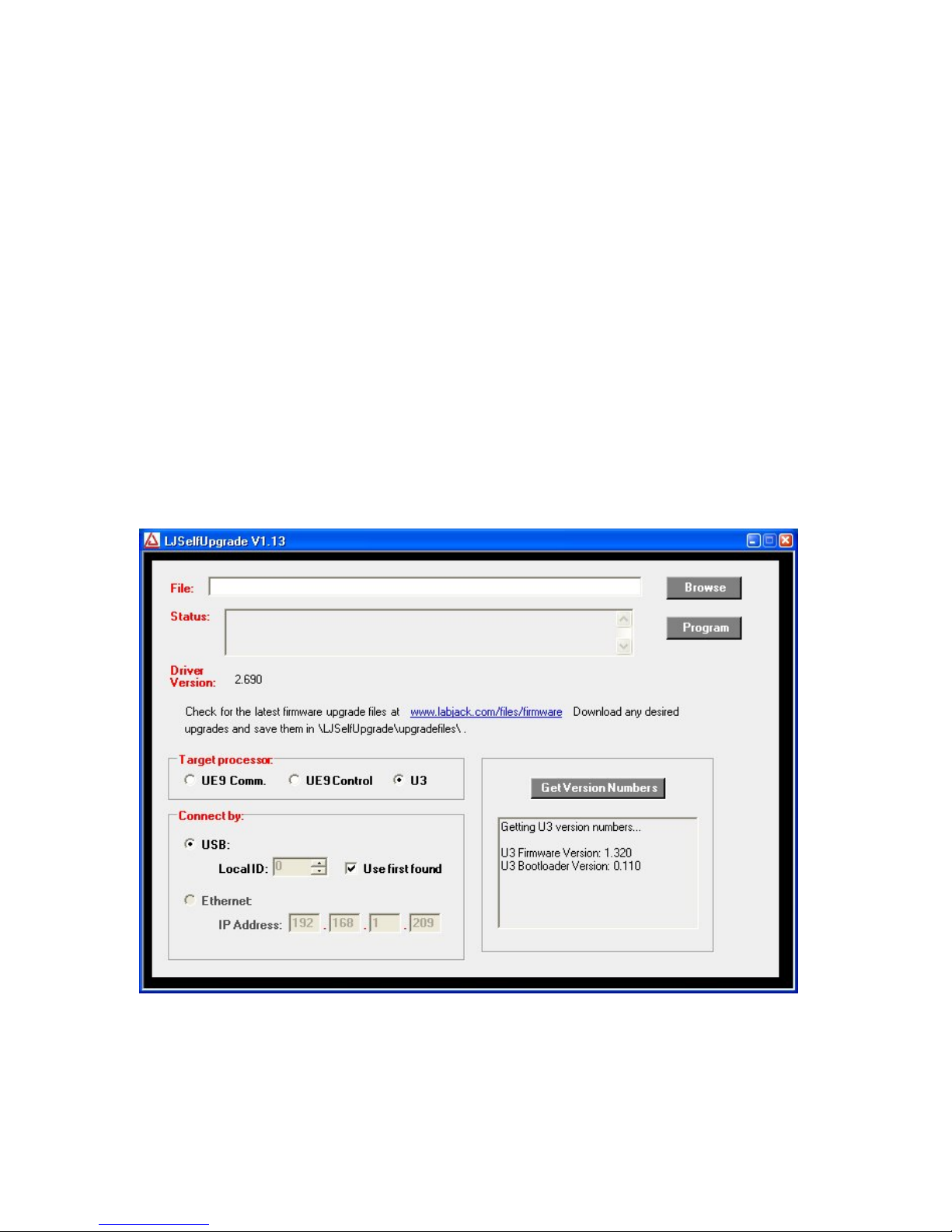
The processor in the U3 has field upgradeable flash memory. The self-upgrade application
shown in Figure 1-5 programs the latest firmware onto the processor.
USB is the only interface on the U3, and first found is the only option for self-upgrading the U3,
so no changes are needed in the “Connect by:” box. There must only be one U3 connected to
the PC when running LJSelfUpgrade.
Click on “Get Version Numbers”, to find out the current firmware versions on the device. Then
use the provided Internet link to go to labjack.com and check for more recent firmware.
Download firmware files to the …\LabJack\LJSelfUpgrade\upgradefiles\ directory.
Click the Browse button and select the upgrade file to program. Click the Program button to
begin the self-upgrade process.
Figure 1-5. Self-Upgrade Application
If problems are encountered during programming, try the following:
1. Unplug the U3, wait 5 seconds then reconnect the U3. Click OK then press
program again.
10
Page 11

2. If step 1 does not fix the problem unplug the U3 and watch the LED while
plugging the U3 back in. Follow the following steps based on the LED's activity.
a. If the LED is blinking continuously, connect a jumper between FIO0
and SCL then unplug the U3, wait 5 seconds and plug the U3 back in.
b. If the LED blinks several times and stays on, connect a jumper
between FIO1 and SCL then unplug the U3, wait 5 seconds and plug the
U3 back in.
c. If the LED blinks several times and stays off, the U3 is not
enumerating. Please restart your computer and try to program again.
d. If there is no LED activity, connect a jumper between FIO1 and SCL
then unplug the U3, wait 5 seconds and plug the U3 back in. If the LED is
blinking continuously click OK and program again. If the LED does not
blink connect a jumper between FIO0 and SCL then unplug the U3, wait 5
seconds and plug the U3 back in.
3. If there is no activity from the U3's LED after following the above steps, please
contact support.
11
Page 12
2. Hardware Description
The U3 has 3 different I/O areas:
• Communication Edge,
• Screw Terminal Edge,
• DB Edge.
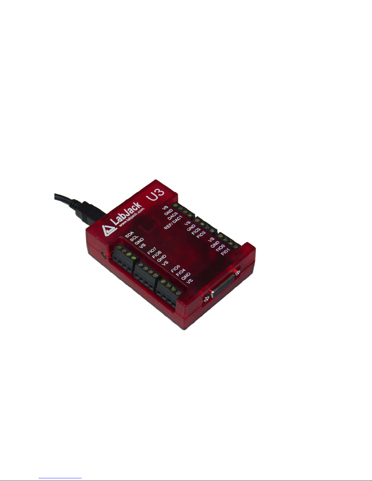
The communication edge has a USB type B connector (with black cable connected in Figure 2-
1). All power and communication is handled by the USB interface.
The screw terminal edge has convenient connections for the analog outputs and 8 flexible I/O
(digital I/O, analog inputs, timers, or counters). The screw terminals are arranged in blocks of 4,
with each block consisting of Vs, GND, and two I/O. There is also a status LED located on the
left edge.
The DB Edge has a D-sub type connectors called DB15 which has the 8 EIO lines and 4 CIO
lines. The EIO lines are flexible like the FIO lines, while the CIO are dedicated digital I/O.
Figure 2-1. LabJack U3
2.1 USB
The U3 has a full-speed USB connection compatible with USB version 1.1 or 2.0. This
connection provides communication and power (Vusb). USB ground is connected to the U3
ground (GND), and USB ground is generally the same as the ground of the PC chassis and AC
mains.
The details of the U3 USB interface are handled by the high level drivers (Windows LabJackUD
DLL), so the following information is really only needed when developing low-level drivers.
12
Page 13

The USB interface consists of the normal bidirectional control endpoint 0 and two bidirectional
bulk endpoints: Endpoint 1 and Endpoint 2. Endpoint 1 consists of a 128 byte OUT endpoint
and a 128 byte IN endpoint. Endpoint 2 consists of a 0 byte OUT endpoint and a 256 byte IN
endpoint. Endpoint 2 OUT is not supported by the firmware, and should never be used.
All commands should always be sent on Endpoint 1, and the responses to commands will also
always be on Endpoint 1. Endpoint 2 is only used to send stream data from the U3 to the host.
2.2 Status LED
There is a green status LED on the LabJack U3. This LED blinks on reset, and then remains
steadily lit.
2.3 GND and SGND
The GND connections available at the screw-terminals and DB connectors provide a common
ground for all LabJack functions. This ground is the same as the ground line on the USB
connection, which is often the same as ground on the PC chassis and therefore AC mains
ground.
SGND is located on the screw terminal block with SDA and SCL. This terminal has a selfresetting thermal fuse in series with GND. This is often a good terminal to use when connecting
the ground from another separately powered system that could unknowingly already share a
common ground with the U3.
See the AIN, DAC, and Digital I/O Sections for more information about grounding.
2.4 Vs
The Vs terminals are designed as outputs for the internal supply voltage (nominally 5 volts).
This will be the voltage provided from the USB cable. The Vs connections are outputs, not
inputs. Do not connect a power source to Vs in normal situations. All Vs terminals are the
same.
2.5 Flexible I/O (FIO/EIO)
The first 16 I/O lines (FIO and EIO ports) on the LabJack U3 can be individually configured as
digital input, digital output, or analog input. In addition, up to 2 of these lines can be configured
as timers, and up to 2 of these lines can be configured as counters. If a line is configured as
analog, it is called AINx according to the following table:
AIN0 FIO0 AIN8 EIO0
AIN1 FIO1 AIN9 EIO1
AIN2 FIO2 AIN10 EIO2
AIN3 FIO3 AIN11 EIO3
AIN4 FIO4 AIN12 EIO4
AIN5 FIO5 AIN13 EIO5
AIN6 FIO6 AIN14 EIO6
AIN7 FIO7 AIN15 EIO7
Table 2-1. Analog Input Pin Locations
13
Page 14

Timers and counters can appear on various pins, but other I/O lines never move. For example,
Timer1 can appear anywhere from FIO0 to EIO1, depending on TimerCounterPinOffset and
whether Timer0 is enabled. On the other hand, FIO5 (for example), is always on the screw
terminal labeled FIO5, and AIN5 (if enabled) is always on that same screw terminal.
The first 8 flexible I/O lines (FIO0-FIO7) appear on built-in screw terminals. The other 8 flexible
I/O lines (EIO0-EIO7) are available on the DB15 connector.
Many software applications will need to initialize the flexible I/O to a known pin configuration.
That requires calls to the low-level functions ConfigIO and ConfigTimerClock. Following are the
values to set the pin configuration to the factory default state:
Byte #
6 WriteMask 15 Write all parameters.
8 TimerCounterConfig 0 No timers/counters. Offset=0.
9 DAC1Enable 0 DAC1 disabled.
10 FIOAnalog 0 FIO all digital.
11 EIOAnalog 0 EIO all digital.
able 2-2. ConfigIO Factory Default Values
T
Byte #
8 TimerClockConfig 130 Set clock to 48 MHz.
9 TimerClockDivisor 0 Divisor = 0.
T
able 2-3. ConfigTimerClock Factory Default Values
hen using the high-level LabJackUD driver, this could be done with requests to the following
W
IOTypes:
Put (lngHandle, LJ_ioPUT_CONFIG, LJ_chNUMBER_TIMERS_ENABLED, 0, 0);
e
ePut (lngHandle, LJ_ioPUT_CONFIG, LJ_chTIMER_COUNTER_PIN_OFFSET, 0, 0)
ePut (lngHandle, LJ_ioPUT_CONFIG, LJ_chTIMER_CLOCK_BASE, LJ_tc48MHZ, 0);
ePut (lngHandle, LJ_ioPUT_CONFIG, LJ_chTIMER_CLOCK_DIVISOR, 0, 0);
ePut (lngHandle, LJ_ioPUT_COUNTER_ENABLE, 0, 0, 0);
ePut (lngHandle, LJ_ioPUT_COUNTER_ENABLE, 1, 0, 0);
ePut (lngHandle, LJ_ioPUT_DAC_ENABLE, 1, 0, 0);
16);
ePut (lngHandle, LJ_ioPUT_ANALOG_ENABLE_PORT, 0,
0,
;
or with a single request to the following IOType created exactly for this purpose:
…
Put (lngHandle, LJ_ioPIN_CONFIGURATION_RESET, 0, 0, 0);
e
2.6 AIN
The LabJac
EIO0-EIO7). Single-ended measurements can be taken of any line compared to ground, or
differential measurements can be taken of any line to any other line.
A
nalog input resolution is 12-bits. The range of single-ended analog inputs is typically 0-2.44 or
0-3.6 volts, and the range of differential analog inputs is typically +/- 2.4 volts. The differential
input range is pseudobipolar, not true bipolar, as for valid measurements the voltage on every
analog input pin, with respect to ground, must be within -0.3 to +3.6 volts. See Appendix A for
voltage limits to avoid damage.
k U3 has up to 16 analog inputs available on the flexible I/O lines (FIO0-FIO7 and
14
Page 15

The analog inputs have a QuickS
e
xpense of increased noise. This is enabled by passing a nonzero value for put_config special
channel
LJ_chAIN_RESOLUTION. There is also a LongSettling option where additional settling
ample option where each conversion is done faster at the
time is added between the internal mulitplexer configuration and the analog to digital
conversion. This allows signals with more source impedance, and is enabled by passing a
nonzero value for put_config special channel
LJ_chAIN_SETTLING_TIME. Both of these
options
are disabled by default.
.6.1 Channel Numbers
2
The LabJack U3 has up to 16 ex
level functions specify a positive
ternal analog inputs, plus a few internal channels. The low-
and negative channel for each analog input conversion. With
the LabJackUD driver, the IOType LJ_ioGET_AIN is used for single-ended channels only, and
thus the negative channel is set to 31. There is an additional IOType called
LJ_ioGET_AIN_DIFF
that allows the user to specify the positive and negative channel.
Positive Channel #
0-7 AIN0-AIN7 (FIO0-FIO7)
8-15 AIN8-AIN15 (EIO0-EIO7)
30 Temp Sensor
31 Vreg
Table 2-4. Positive Channel Numbers
Channel 31 puts the internal Vreg (~3
2
.6.4 for information about the internal temperature sensor.
.3 volts) on the positive input of the ADC. See Section
Negative Channel #
0-7 AIN0-AIN7 (FIO0-FIO7)
8-15 AIN8-AIN15 (EIO0-EIO7)
30 Vref
31 Single-Ended
32 Special 0-3.6 (UD Only)
Table 2-5. Negative Channel Numbers
If the negative channel is set to anythin
re
turns a pseudobipolar value. If the negative channel is set to 31, the U3 does a single-ended
g besides 31, the U3 does a differential conversion and
conversion returns a unipolar value. Channel 30 puts the internal voltage reference Vref (~2.44
volts) on the negative input of the ADC.
Channel 32 is a special negative channe
d
river will actually pass 30 as the negative channel to the U3, and when the result is returned
the driver adds Vref to the value. This results is a full span on the positive channel of about 0
l supported by the LabJack driver. When used, the
to
4.88 volts (versus ground), but since the voltage on any analog input cannot exceed 3.6 volts,
only 75% of the converters range is used and the span is about 0 to 3.6 volts.
.6.2 Converting Binary Readings to Voltages
2
Following are the nominal input voltage ranges for the analog inputs, assuming that DAC1 is not
enabled.
15
Page 16

Max V Min V
Single-Ended 2.44 0.0
Differential 2.44 -2.44
Special 0-3.6 3.6 0.0
Table 2-6. Nominal Analog Input Voltage Ranges (DAC1 Disabled)
Note that the minimum
can be as
much as 2.44 volts less than the negative channel, not that a channel can measure
2.44 volts less than ground. The voltage of any analog input pin, c
in
the range -0.3 to +3.6 volts.
differential input voltage of -2.44 volts means that the positive channel
ompared to ground, must be
The “Special 0-3.6” range is obtained by doing a differential measurement where the negative
channel is set to the internal Vref (2.44 volts).
A
lthough the binary readings ha
ve 12-bit resolution, they are returned justified as 16-bit values,
so the approximate nominal conversion from binary to voltage is:
olts(uncalibrated) = (Bits/65536)*Span
V
(Single-Ended)
Volts(uncalibrated) = (Bits/65536)*Span – Span/2 (Differential)
Where span is the maximum voltage minus the minimum voltage fro
a
ctual nominal conversions are provided he s below, and sh
in t table ould be used if the actual
calibration constants are not read for some reason. Most applications wi
c
alibrations constants (Slope and Offset) stored in the internal flash.
m the table above. The
ll use the actual
Volts = (Slope * Bits) + Offset
Since the U3 uses multiplexed channels connected to a single analog-to-digital converter
ADC), all channels have the same calibration for a given configuratio
(
n.
T
able 2-4 shows where the var
when communication is initiated with the U3, three calls will be made to the ReadMem func
to retrieve the first 3 blocks of memory. This information can then be used to convert all a
put readings to voltages. The high level Windows DLL (LabJackUD) do
in
ious calibration values are stored in the Mem area. Generally
tion
nalog
es this automatically.
Starting
Block #
0 0 AIN SE Slope 3.7231E-05 volts/bit
0 8 AIN SE Offset 0.0000E+00 volts
0 16 AIN Diff Slope 7.4463E-05 volts/bit
0 24 AIN Diff Offset -2.4400E+00 volts
1 0 DAC0 Slope 5.1717E+01 bits/volt
1 8 DAC0 Offset 0.0000E+00 bits
1 16 DAC1 Slope 5.1717E+01 bits/volt
1 24 DAC1 Offset 0.0000E+00 bits
2 0 Temp Slope 1.3021E-02 degK/bit
2 8 Vref @Cal 2.4400E+00 volts
2 16 Vref*1.5 @Cal 3.6600E+00 volts
2 24 Vreg @Cal 3.3000E+00 volts
Byte Nominal Value
Table 2-7. Calibration Constant Memory Locations
16
Page 17

Each value in Table 2.4 is stored in 64-bit fixed point format (signed 32.32, little endian, 2’s
omplement). Following are some examples of fixed point byte arrays and the associated
c
floating point double values.
Fixed Point B
{0,0,0,0,0,0,0,0} 0.0000000000
{0,0,0,0,1,0,0,0} 1.0000000000
{0,0,0,0,255,255,255,255} -1.0000000000
{51,51,51,51,0,0,0,0} 0.2000000000
{205,204,204,204,255,255,255,255} -0.2000000000
{73,20,5,0,0,0,0,0} 0.0000775030
{225,122,20,110,2,0,0,0} 2.4300000000
{102,102,102,38,42,1,0,0} 298.1500000000
Table 2-8. Fixed Point Conversion Examples
yte Array
(LSB, …, MSB)
Floating Point Double
.6.2.1 Analog Inputs With DAC1 Enabled
2
he previous information assumed that DAC1 is disabled. If DAC1 is enabled, then the internal
T
reference (Vref = 2.44 volts) is not available for the
ADC, and instead the internal regulator
voltage (Vreg = 3.3 volts) is used as the reference for the ADC. Vreg is not as stable as Vref,
but more stable than Vs (5 volt power supply). Following are the nominal input voltage ranges
for the analog inputs, assuming that DAC1 is enabled.
Max V Min V
Sin
gle-Ended 3.3 0.0
ferential 3.3 -3.3
Dif
Special 0-3.6 3.6 0.0
Table 2-9. Nominal Analog Input
Voltage Ranges (DAC1 Enabled)
Note that the minimum differential input voltage of -3.3 volts mean
an be as much as 3.3 volts less than the negative channel, not that a channel can measure 3.3
c
volts less than ground. The voltage of any analog input pin, compared to ground, must be in t
s that the positive channel
he
range -0.3 to +3.6 volts, for specified performance. See Appendix A for voltage limits to avoid
damage.
The “Special 0-3.6” range is obtained by doing a differential measurement where the negative
c
hannel is
set to the ADC reference, which with DAC1 enabled is Vreg. This results is a full
span on the positive channel of about 0 to 6.6 volts (versus ground), but since the voltage on
any analog input cannot exceed 3.6 volts, only 55% of the converters range is used and the
span is about 0 to 3.6 volts.
When DAC1 is enabled, the slope/offset calibration constants are not used to convert raw
r
eadings to voltages. Rather
, the Vreg value is retrieved from the Mem area, and used with the
approximate single-ended or differential conversion equations above, where Span is Vreg
(single-ended) or 2Vreg (differential).
.6.3 Typical Analog Input Co2
nnections
A common question is “can this sensor/signal be measured with the U3”. Unless the signal has
a voltage (referred to U3 ground) beyond the limits in Appendix A, it can be connected without
17
Page 18

damaging the U3, but more thought is required to determine what is necessary to make useful
measurements with the U3 or any measurement device.
Voltage (versus ground): The single-ended analog inputs on the U3 measure a voltage with
respect to U3 ground. The differential inputs measure the voltage difference between two
hannels, but the voltage on each channel with respect to
c ground must still be within the
common mode limits specified in Appendix A. When measuring parameters other than voltag
or voltages too big or too small for the U3, some sort of sensor or transducer is required to
produce the proper voltage signal. Examples are a temperature sensor, amplifier, resistive
voltage divider, or perhaps a combination of such things.
Impedance: When connecting the U3, or any measuring device, to a signal source, it must b
considered what impact the measuring device will have on the signal. The main consideratio
whether the currents going into or out of the U3 analog in
is
errors due to the impedance of the source. To maintain consistent 12-bit results, it is
recommended to keep the source impedance less than 10 kΩ.
Resolution (and Accuracy): Based on the measurement type and resolution of the U3, the
resolution can be determined in terms of voltage or engineering units. For example, a
s
ome temperature sensor provides a 0-10 mV signal, correspon
Samples are then acquired with the U3 using the 0-2.44 volt single-ended input range, resu
in a voltage resolution of about 2.44/4096 = 596 μV. That means there will be about 17 discre
steps across the 10 mV span of the signal, and the temperature resolution is about 6 degrees
If this experiment required a resolution of 1 degrees C, this configuration would not be sufficient.
Accuracy will also need to be considered. Appendix A places some boundaries on expected
accuracy, but an in-system calibration can generally be done to provide absolute accuracy down
to the INL limits of the U3.
Speed: How fast does the signal need to be sampled? For instance, if the signal is a
waveform, what information is needed: peak, average, RMS, shape, frequency, … ? Answers
o these questions will help
t decide how many points are needed per waveform cycle, and thus
what sampling rate is required. In the case of multiple channels, the scan rate is also
considered. See Sections 3.1 and 3.2.
put will cause noticeable voltage
ssume
ding to 0-100 degrees C.
e,
e
n
lting
te
C.
2.6.3.1 Signal from the LabJack
ne example of measuring a signal from the U3 itself, is with O
3 share a common ground, so the voltage on an analog output (DAC) can be measured by
U
simply connecting a single wire from th
output must be set to a voltage within the range of the analog input.
at terminal to an AIN terminal (FIO/EIO). The analog
an analog output. All I/O on the
2.6.3.2 Unpowered isolated signal
n example of an unpowered isolated signal would be a photocell where A
ot shorted to any external voltages. Such a sensor typically has two leads, where the positive
n
lead connects to an AIN terminal and the
negative lead connects to a GND terminal.
the sensor leads are
2.6.3.3 Signal powered by the LabJack
typical example of this type of signal is a 3-wire temperature sensor. The sensor has a power A
nd ground wire that connect to Vs and GND on the LabJack, and then has a signal wire that
a
simply connects to an AI
N terminal.
18
Page 19

Another variation is a 4-wire sensor where there are two signal wires (positive and negative)
rather than one. If the negative signal is the same as power ground, or can be shorted ground,
then the positive signal can be connected to AIN and a single-ended measurement can be
made. A typical example where this
ensor, providing the raw bridge output (and no amplifier). In this case the signal voltage is the
s
difference between the positive and negative signal, and the negative signal cannot be shorte
does not work is a bridge type sensor, such as pressure
d
to ground. Such a signal could be measured using a differential input on the U3.
2.6.3.4 Signal powered externally
An example is a box with a wire coming out that is defined as a 0-5 volt analog signal and a
second wire labeled as ground. The signal is known to have 0-5 volts compared t
ire, but the complication is what is the voltage of the box ground compared to the LabJack
w
round.
g
o the ground
If the box is known to be electrically isolated from the LabJack, the box ground can simply be
connected to LabJack GND. An example would be if the box was plastic, powered by an
internal battery, and does not have any wires besides the signal and ground which are
connecte
d to AINx and GND on the LabJack.
If the box ground is known to be the same as the LabJack GND, then perhaps only the one
signal wire needs to be connected to the LabJack, but it generally does not hurt to go ahea
and connect the ground wire to LabJack GND with a 100 Ω resistor. You definitely do n
d
ot want
to connect the grounds without a resistor.
If little is known about the box ground, a DMM can be used to measure the voltage of box
ground compared to LabJack GND. As long as an extreme voltage is not measured, it is
generally OK to connect the box ground to LabJack GND, but it is a good idea to put in a 100 Ω
series resistor to prevent large currents fro
sistor (typically 1/8 or 1/4 watt) so that it blows if too much current does flow. The only
re
current that should flow on the ground is the return of the analog input bias current, which i
m flowing on the ground. Use a small wattage
s on
the order of … for the U3.
The SGND terminal (on the same terminal block as SDA/SCL) can be used instead of GND
for
externally powered signals. A series resistor is not needed as SGND is fused to prevent
overcurrent, but a resistor will eliminate confusion that can be caused if the fuse is tripping and
resetting.
In general, if there is uncertainty, a good approach is to use a DMM to measure the voltage on
each signal/ground wire without any connections to the U3. If no large voltages are noted
,
connect the ground to U3 SGND with a 100 Ω series resistor. Then again use the DMM to
measure th
e voltage of each signal wire before connecting to the U3.
Another good general rule is to use the minimum number of ground connections. For instance,
if connecting 8 sensors powered by the same external supply, or otherwise referred to the s
ame
external ground, only a single ground connection is needed to the U3. Perhaps the ground
leads from the 8 sensors would be twisted together, and then a single
a 100 Ω resistor which is connected to U3 ground.
to
wire would be connected
2.6.3.5 Amplifying small signal voltages
The best results are generally obtained when a signal voltage spans the full analog input range
of the LabJack. If the signal is too small it can be amp
lified before connecting to the LabJack.
19
Page 20
One good way to handle low-level signals such as thermocouples is the LJTick-InAmp, which is
2-channel instrumentation amplifier module that plugs into the U3 screw-terminals. Go to
a
labjack.com for more information.
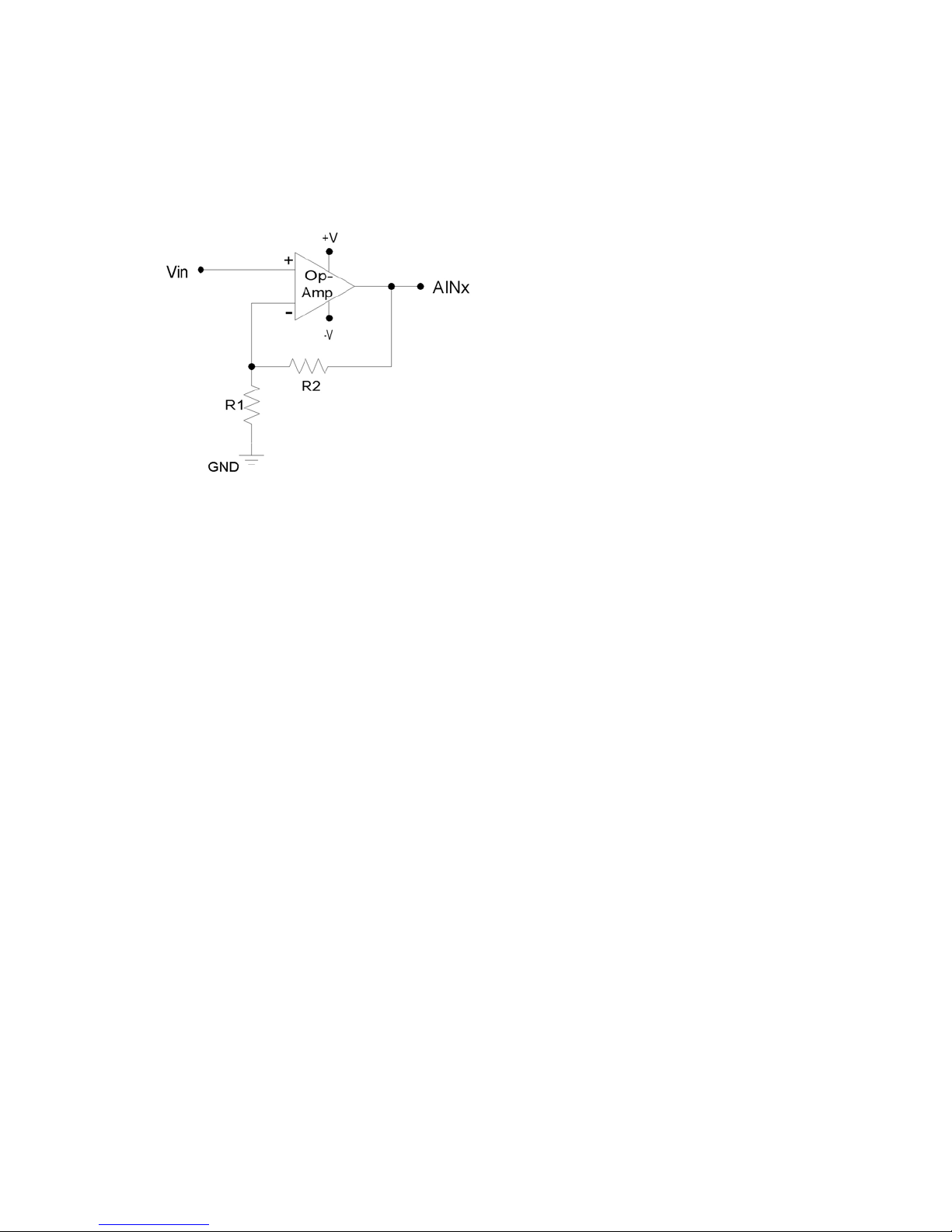
For a do-it-yourself solution, the following figure shows an operational amplifier (op-amp)
configured as non-inverting:
Figure 2-2. Non-Inverting Op-Amp Configuration
The gain of this configuration is:
Vout = Vin * (1 + (R2/R1))
00 kΩ is a typical value for R2. Note that if R2=0 (short-circuit) and R1=inf (not installed), a
1
simple buffer with a gain equal to
1 is the result.
There are numerous criteria
O
ne of the main criteria is that the op-amp can handle the input and output signal range. Often,
used to choose an op-amp from the thousands that are available.
a single-supply rail-to-rail input and output (RIRO) is used as it can be powered from Vs and
GND and pass signals within the range 0-Vs. Th
g
ood for many 5 volt applications.
e OPA344 from Texas Instruments (ti.com) is
The op-amp is used to amplify (and buffer) a signal that is referred to the same ground as the
LabJack (single-ended). If instead the signal is differential (i.e. there is a positive and negativ
e
signal both of which are different than ground), an instrumentation amplifier (in-amp) should be
used. An in-amp converts a differen
m
ethod to set gain.
tial signal to single-ended, and generally has a simple
2.6.3.6 Signal voltages beyond 0-2.44 volts (and resistance measurement)
The nominal maximum analog input voltage range for the U3 is 0-2.44 volts. The easiest w
handle larger voltage
d
ivider module that plugs into the U3 screw-terminals. More information is available at
la
bjack.com.
s is often by using the LJTick-Divider, which is a two channel buffered
The basic way to handle higher unipolar voltages is with a resistive voltage divider. The
following figure shows the resistive voltage divider assuming that the source voltage (Vin) is
referred to the same ground as the U3 (GND).
ay to
20
Page 21
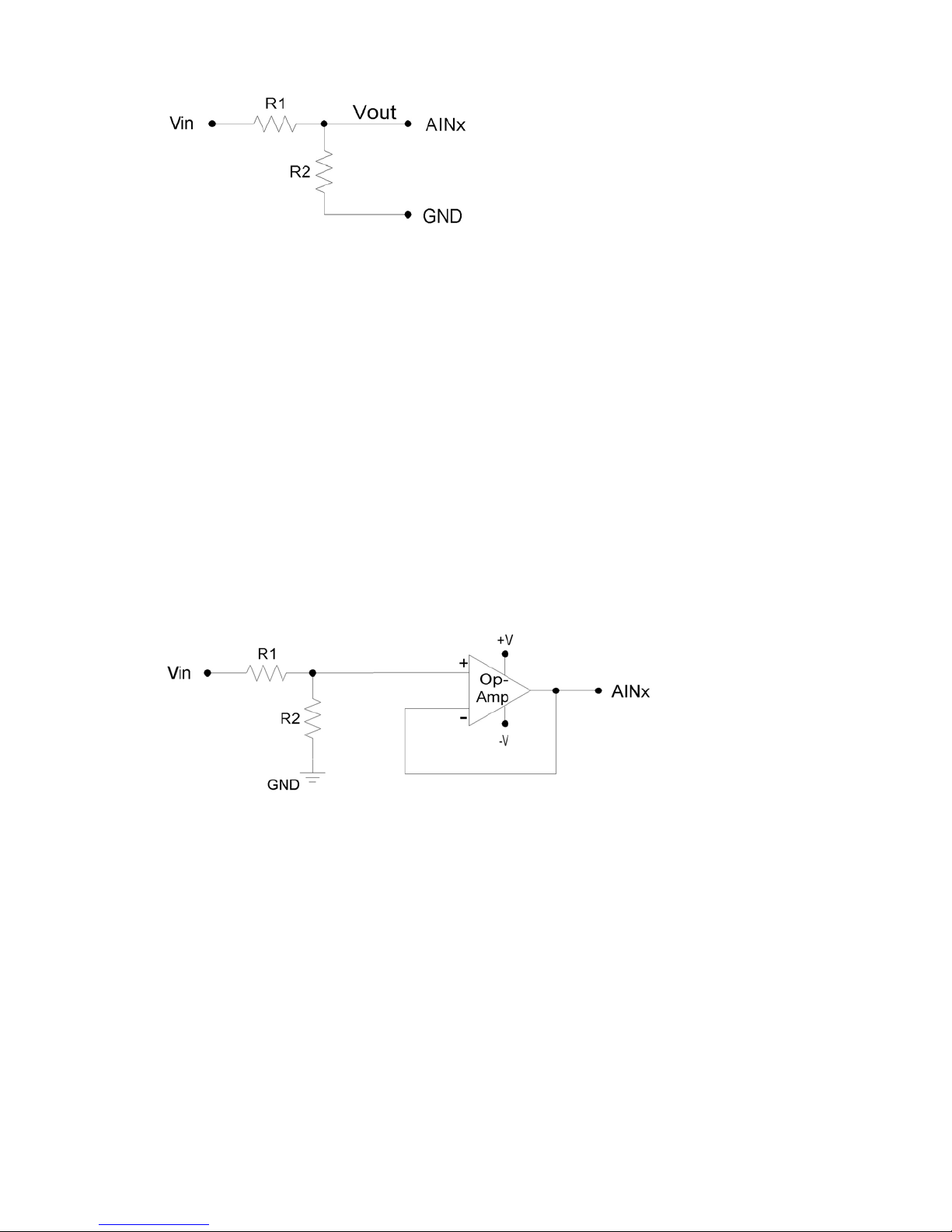
Figure 2-3. Voltage Divider Circuit
The attenuation of this circuit is determined by the equation:
Vout = Vin * ( R2 / (R1+R2))
his divider is easily implemented by putting a resistor (R1) in series with the signal wire, and
T
placing a second resistor (R2) from the AIN terminal to a GND
nalog input performance, R1 should not exceed 10 kΩ, so R1 can generally be fixed at 10 kΩ
a
and R2 can be adjusted for th
ivide by 2.1, so a ~0-5 volt input will be scaled to the input range of the U3.
d
e desired attenuation. For instance, R2 = 9.1 kΩ provides a
terminal. To maintain specified
The divide by 2 configuration where R1 = R2 = 10 kΩ, presents a 20 kΩ load to the source,
meaning that a 5 volt signal will have to be able to source/sink up to
sources might require a load with higher resistance, in which case a buffer should be used.
following figure shows a resistive voltage divider followed by an op-amp confi
verting unity-gain (i.e. a buffer).
in
+250 µA. Some signal
The
gured as non-
Figure 2-4. Buffered Voltage Divider Circuit
The op-amp is chosen to have low input bias currents so that large resistors can be used in the
voltage divider. For 0-5 volt applications, where the amp will be powered from Vs and GND, a
good choice would be the OPA344 from Tex
small bias current that changes little across
th
e amp from Vs and GND, the input and output to the op-amp is limited to that range, so if Vs is
4.8 volts your signal range will be 0-4.8 volts.
The information above also applies to resistance measurement. A common way to measure
resistance is to build a voltage divider as shown in Figure 2-4, where one of the resistors is
known and the other is the unknown. If Vin is known and Vout is measured, the voltage divider
equation can be rearranged to solve for the unk
21
as Instruments (ti.com). The OPA344 has a very
the entire voltage range. Note that when powering
nown resistance.
Page 22
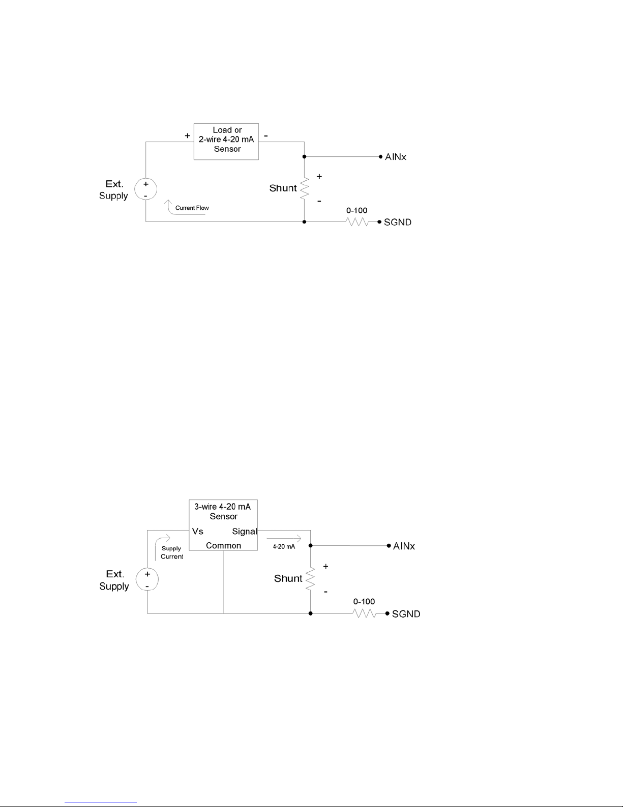
2.6.3.7 Measuring current (including 4-20 mA) with a resistive shunt
The following figure shows a typical method to measure the current through a load, or to
m
easure the 4-20 mA signal produced by a 2-wire (loop-powered) current loop sensor. The
urrent shunt shown in the figure is simply a resistor.
c
Figure 2-5. Current Measurement With Arbitrary Load or 2-Wire 4-20 mA Sensor
When measuring a 4-20 mA signal, a typical value for the shunt would be 120 Ω. This results in
a 0.48 to 2.40 volt signal corresponding to 4-20 mA. The external supply must p
voltage for the sensor and the shunt, so if the sensor requires 5 volts the supply
le
ast 7.4 volts.
For applications besides 4-20 mA, the shunt is chosen based on the maximum current and how
much voltage drop can be tolerated across the shunt. For instance, if the maximum current is
1.0 amp, and 1.
Ω
resistor could be used. That equates to 1.0 watts, though, which would require a special high
0 volts of drop is the most that can be tolerated without affecting the load, a 1.0
wattage resistor. A better solution would be to use a 0.1 Ω shunt, and then use an amplifier to
increase the small voltage produced by that shunt. If the maximum current to measure is too
high (e.g. 100 amps), it will be difficult to find a small enough resistor and a hall-effect sensor
should be considered instead of a shunt.
The following figure shows typical connections for a 3-wire 4-20 mA sensor. A typical value fo
the shunt would be 120 Ω which results in 0.48 to 2.40 volts.
rovide enough
must provide at
r
Figure 2-6. Current Measurement With 3-Wire 4-20 mA (Sourcing) Sensor
The sensor shown in Figure 2-6 is a sourcing type, where the signal sources the 4-20 mA
current which is then sent through the shunt resistor and sunk into ground. Another type of 3wire sensor is the sinking type, where the 4-20 mA current is sourced from
sent through the shunt resistor, and then sunk into the signal wire. If sen
connected to U3 ground, the sinking type of sensor presents a problem, as at least one sid
the resistor has a high common mode voltage (equal to the positive sensor supply). If the
sensor is isolated, a possible solution is to connect the sensor signal or positive sensor supply
22
the positive supply,
sor ground is
e of
Page 23

to U3 ground (instead of sensor ground). This requires a good understanding of ground
isolation in the system. The LJTick-CurrentShunt is often a simple solution.
Both Figure 2-5 and 2-6 show a 0-100 Ω resistor in series with SGND, which is discussed in
general in Section 2.6.3.4. In this case, if SGND is used (rather than GND), a direct connection
(0 Ω) should be good.
The best way to handle 4-20 mA signals is with the LJTick-CurrentShunt, which is a two chan
active current to voltage converter module that plugs into the U3 screw-terminals. More
information is available
at labjack.com.
ing and
nel
2.6.3.8 Floating/Unconnected Inputs
The reading from a floating (no external
p
redict and is likely to vary with sample timing and adjacent sampled channels. Keep in mind
th
at a floating channel is not at 0 volts, but rather is at an undefined voltage. In order to see 0
volts, a 0 volt signal (such as GND) should
Some data acquisition devices use a resistor, from the input to ground, to bias an unconnected
input to read 0. This is often just for "cosmetic" reasons so that the input reads close to 0 with
floating inputs, and a reason not to do that is that this resistor can degr
o
f the analog input.
In a situation where it is desired that a floating channel read a particular voltage, say to detect a
broken wire, a resistor can be placed from the AINx screw terminal to the desired voltage (GND,
VS, DACx, ...). A 10
d
esired voltage, but obviously degrades the input impedance to 100 kΩ. For the specific case
of pulling a floating channel to 0 volts, a 1 MΩ resistor to GND can typically be used to provide
analog input readings of less than 50 mV.
0 kΩ resistor should pull the analog input readings to within 50 mV of any
connection) analog input channel can be tough to
be connected to the input.
ade the input impedance
2.6.4 Internal Temperature Sensor
he U3 has an internal temperature sensorT
in
side the U3, which is warmer than ambient, it has been calibrated to read actual ambient
temperature. For accurate measurements th
relative to the ambient temperature, which ca
obtained in still air in an environment with slowly changing ambient temperatures.
With the UD driver, the internal temperature sensor is read by acquiring single-ended analo
input channel 30, and returns degrees K.
. Although this sensor measures the temperature
e temperature of the entire U3 must stabilize
n take on the order of 1 hour. Best results will be
g
2.7 DAC
he LabJack U3 has 1 or 2 analog outputsT
te
rminals. Each analog output can be set to a voltage between about 0.04 and 4.95 volts with
8-bits of reso
The second analog output is only available in certain configurations. In particular, if the analog
inputs are using the internal 2.4 volt reference (the most accurate option), then DAC1 outputs a
fixed voltage of 1.5*Vref. If DAC1 is enabled, the analog inputs use Vreg (3.3 volts) as the A
re
ference, which is not as stable as the internal 2.4 volt reference.
lution. The maximum output voltage is limited by the supply voltage to the U3.
(DAC0 and DAC1) that are available on the screw
DC
23
Page 24

The DAC outputs are derived as a percentage of Vreg, and then amplified by 1.5, so any
changes in Vreg will have a proportionate affect on the DAC outputs. Vreg is more stable than
Vs (5 volt supply voltage), as it is the output from a 3.3 volt regulator.
The DACs are derived from PWM signals that are affected by the timer clock frequency (Section
2.x). The default timer clock frequency of the U3 is set to 24 MHz, as this results in the
minimum DAC output noise. If the frequency is lowered, the DACs will have more noise, where
the frequency of the noise is the timer clock frequency divided by 2
8
.
The analog outputs have filters with a 3 dB cutoff around 16 Hz, limiting the frequency of output
waveforms to less than that.
The analog output commands are sent as raw binary values (low leve
o
utput voltage, the binary value can be approximated as:
l functions). For a desired
Bits(uncalibrated) = (Volts/4.9
5)*256
For a proper calculation, though, use the calibration values (Slope and Offset) stored in the
internal flash on the processor (Table 2-7):
Bits = (Slope * Volts) + Offset
The analog outputs can withstand a continuous short-circuit to ground, even when set at
maximum output.
Voltage should never be applie
In
the event that a voltage is accidentally applied to either analog output, they do have
d to the analog outputs, as they are voltage sources themselves.
protection against transient events such as ESD (electrostatic discharge) and continuous
overvoltage (or unde
rvoltage) of a few volts.
2.7.1 Typical Analog Output Connections
.7.1.1 High Current Output 2
T
he DACs on the U3 can output quite a bit of current, but have 50 Ω of source impedance that
will cause voltage drop. To avoid this voltage drop, an
such as the non-inverting configuration shown in Figu
b
etween the DAC output and the amp input for further noise reduction. Note that the ability of
the amp to source/sink current ne
ar the power rails must still be considered. A possible op-amp
choice would be the TLV246x family (ti.com).
2.7.1.2 Different Output Ranges
The typical output range of the DACs is about 0.04 to 4.95 volts. For other unipolar ranges, an
op-amp in the non-inverting configuration (Figure 2-3) can be used to provide the desired gain.
For example, to increase the maximum output
re
quired. If R2 (in Figure 2-3) is chosen as 100 kΩ, then an R1 of 97.6 kΩ is the closest 1%
resistor that provides a gain greater th
an 2.02. The +V supply for the op-amp would have to be
greater than 10 volts.
For bipolar output ranges, such as
±10 volts, a similar op-amp circuit can be used to provide
gain and offset, but of course the op-amp must be powered with supplies greater than the
desired output range (depending on the ability of the op-amp to drive it’s outputs close to the
from 4.95 volts to 10.0 volts, a gain of 2.02 is
op-amp can be used to buffer the output,
re 2-2. A simple RC filter can be added
24
Page 25
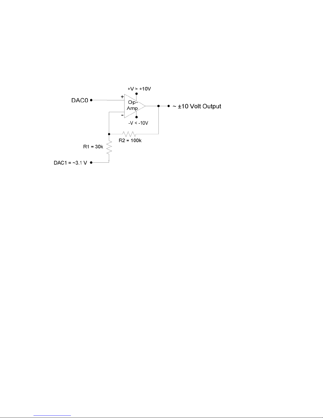
power rails). If
amp (linear.com), which can handle a supply span up to 44 volts.
A reference voltage is also required to provide the offset. In the following circuit, DAC1 is use
to provide a reference voltage. The actual value of DAC1 can be adjusted such that the circu
output is 0 volts at the DAC0 mid-scale voltage, and the value of R
d
esired gain. A fixed reference (such as 2.5 volts) could also be used instead of DAC1.
Figure 2-7. ±10 Volt DAC Output Circuit
±10, ±12, or ±15 volt supplies are available, consider using the LT1490A op-
1 can be adjusted to get the
d
it
A two-point calibration should be done to determine the exact input/output relationship of this
circuit. Ref to application note SLOA097 from ti.com for further information about gain and
offset design with op-amps.
er
2.8 Digital I/O
The LabJack U3 has up to 20 digital I/O channels. 16 are available from the flexible I/O lines,
and 4 dedicated digital I/O (C
can be individually config
logic and are 5 volt t
The LabJackUD driver uses the following bit numbers to specify all the digital lines:
0-7 FIO0-FIO7
8
-15 EIO0-EIO7
16-19 CIO0-CIO3
The 8 FIO lines app
only on the DB15 co
A
ll the digital I/O include an internal series resistor that provides overvoltage/short-circuit
protection. These series resistors also limit the ability of these lines to sink or source current.
Refer to the specifications in Appendix A.
All digital I/O on the U3 have 3 possible states: input, output-high, or output-low. Each bit
can be configured individually. When configured as an input, a bit has a ~100 kΩ pull-up
resistor to 3.3 volts (all digital I/O are 5 volt
c
onnected to the internal 3.3 volt supply (through a series resistor). When configured as output-
low, a bit is connected to GND (through a series resistor).
olerant.
ear on the built-in screw-terminals, while the 8 EIO and 4 CIO lines appear
nnector. See the DB15 Section of this User’s Guide for more information.
IO0-CIO3) are available on the DB15 connector. Each digital line
ured as input, output-high, or output-low. The digital I/O use 3.3 volt
of I/O
tolerant). When configured as output-high, a bit is
25
Page 26

The power-up condition of the digital I/O can be configured by the user. From the factory,
all
digital I/O are configured to power-up as inputs. Note that even if the power-up default for a lin
is changed to output-high or output-low, there is a delay of about xxx ms at power-up where all
digital I/O are in the factory default condition.
The low-level Feedback function (Section 5.2.5) writes and reads all digital I/O. For informatio
about using digital I/O under the Windows LabJackUD driver, see Section 4.3.5. See Section
3.1 for timing information.
M
any function parameters contain specific bits within a single integer parameter to write/read
specific information. In particular, most digital I/O parameters contain the information for each
bit of I/O in one integer, where each bit of I/O corresponds to the same bit in the parameter (e.g
the direction of FIO0 is set
C
onfigU3, the parameter FIODirection is a single byte (8 bits) that writes/reads the power-up
in bit 0 of parameter FIODir). For instance, in the low-level function
direction of each of the 8 FIO lines:
• if FIODirection is 0, all FIO lines are input,
0
• if FIODirection is 1 (2
• if FIODirection is 5 (2
• if FIODirection is 255 (2
), FIO0 is output, FIO1-FIO7 are input,
0
+ 22), FIO0 and FIO2 are output, all other FIO lines are input,
0
+ …
7
), FIO0-FIO7 are output.
+ 2
e
n
.
2.8
.1 Typical Digital I/O Connections
.8 1
2T.1. Input: Driven Signals
he most basic connection to a U3 digital input is a driven signal, often called push-pull. With a
push-pull signal the source is typically providing
logic low. This signal is generally connected dir
v
oltage specifications in Appendix A. If the signal is over 5 volts, it can still be connected with a
series resistor. The digital inputs h
ave protective devices that clamp the voltage at GND and
a high voltage for logic high and zero volts for
ectly to the U3 digital input, considering the
VS, so the series resistor is used to limit the current through these protective devices. For
instance, if a 24 volt signal is connected through a 10 kΩ series resistor, about 19 volts will be
dropped across the resistor, resulting in a current of 1.9 mA, which is no problem for the U3.
The other possible consideration with the basic push-pull signal is the ground connection. If th
signal is known to already have a common ground with the U3, then no additional ground
connection is used. If the signal is known to not have a common ground with the U3, then the
signal ground can simply be connected to U3 GND. If there is uncertainty about the relations
b
etween signal ground and U3 ground (e.g. possible common ground through AC mains), then
a ground connection with a ~10 Ω series resistor is generally recommended (see Section
2.7.3.4).
e
hip
Figure 2-8. Driven Signal Connection To Digital Input
26
Page 27
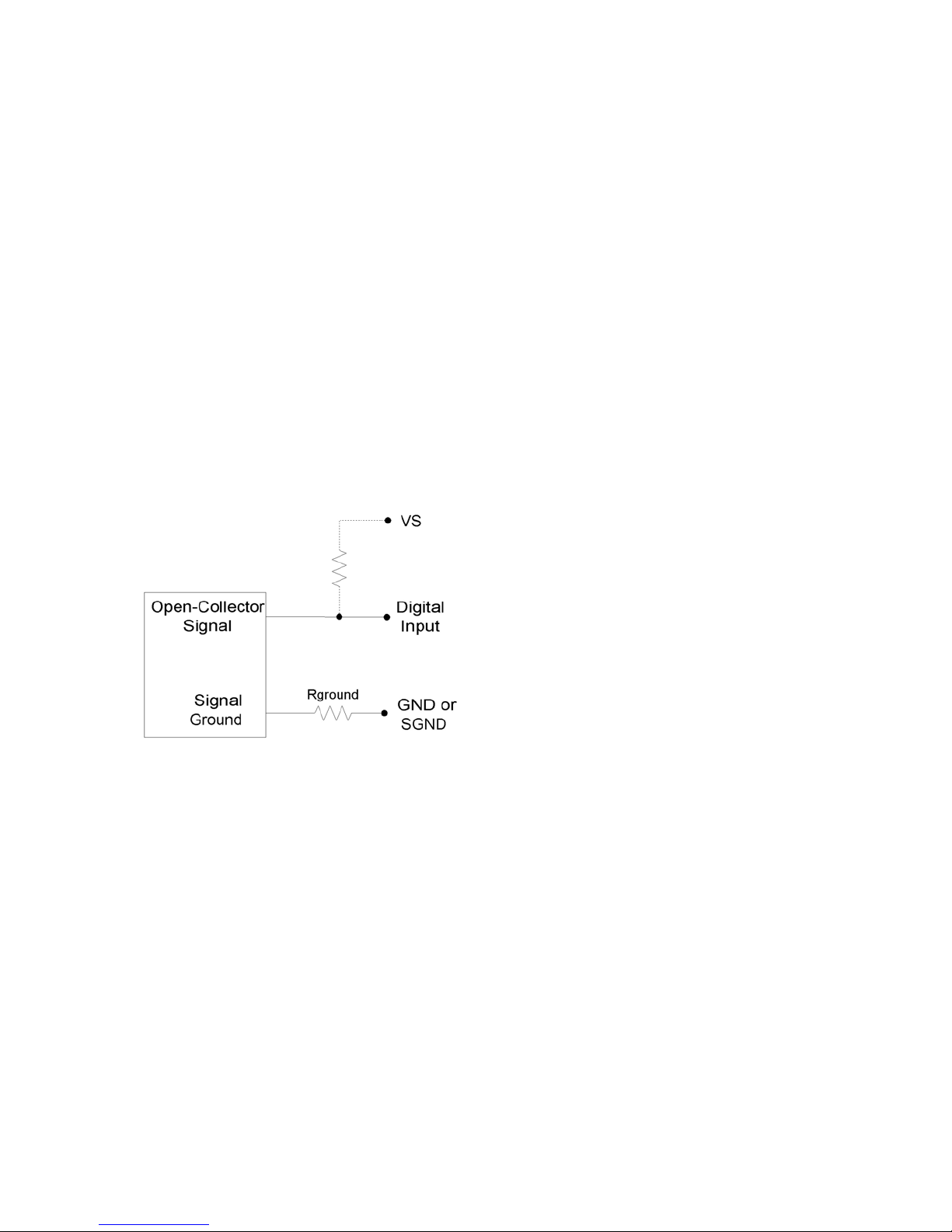
Figure 2-8 shows typical connections. Rground is typically 0-100 Ω. Rseries is typically 0 Ω
(short-circuit) for 3.3/5 volt logic, or 10 kΩ for high-voltage logic. Note that an individual ground
connection is often not needed for every signal. Any signals powered by the same external
supply, or otherwise referred to the same external ground, should share a single ground
connection to the U3 if possible.
When dealing with a new sensor, a push-pull signal is often incorrectly assumed when in fact
the sensor provides an open-collector signal as described ne
xt.
.8.1.2 Input: Open-Collector Signals
2
Open-collector (also called open-drain) is a very common type of digital signal. Rather than
providing 5 volts and ground, like the push-pull signal, an open-collector signal provides ground
and high-impedance. This type of signal can be thought of as a switch connected to ground.
Since the U3 digital inputs have a 100 kΩ internal pull-up resistor, an open-collector signa
generally be connected directly to
oltage and the pull-up resistor pulls the digital input to logic high. When the signal is active, it
v
the input. When the signal is inactive, it is not driving any
drives 0 volts which overpowers the pull-up and pulls the digital input to logic low. Sometimes,
an external pull-up (e.g. 4.7 kΩ from Vs to digital input) will be ins
nd speed of the logic high condition.
a
talled to increase the strength
l can
Figure 2-9. Driven Signal Connection To Digital Input
Figure 2-10 shows typical connections. Rground is typically 0-100 Ω, and the external pull-up
resistor is generally not required. Note that an individual ground connection is often not needed
for every signal. Any signals powered by the same external supply, or otherwise referred to the
same external ground, should share a single ground connection to the U3 if possible.
2.8.1.3 Input: Mechanical Switch Closure
To detect whether a mechanical switch is open or closed,
ground and the other side to a digital input. The beha
escribed above.
d
27
connect one side of the switch to U3
vior is very similar to the open-collector
Page 28
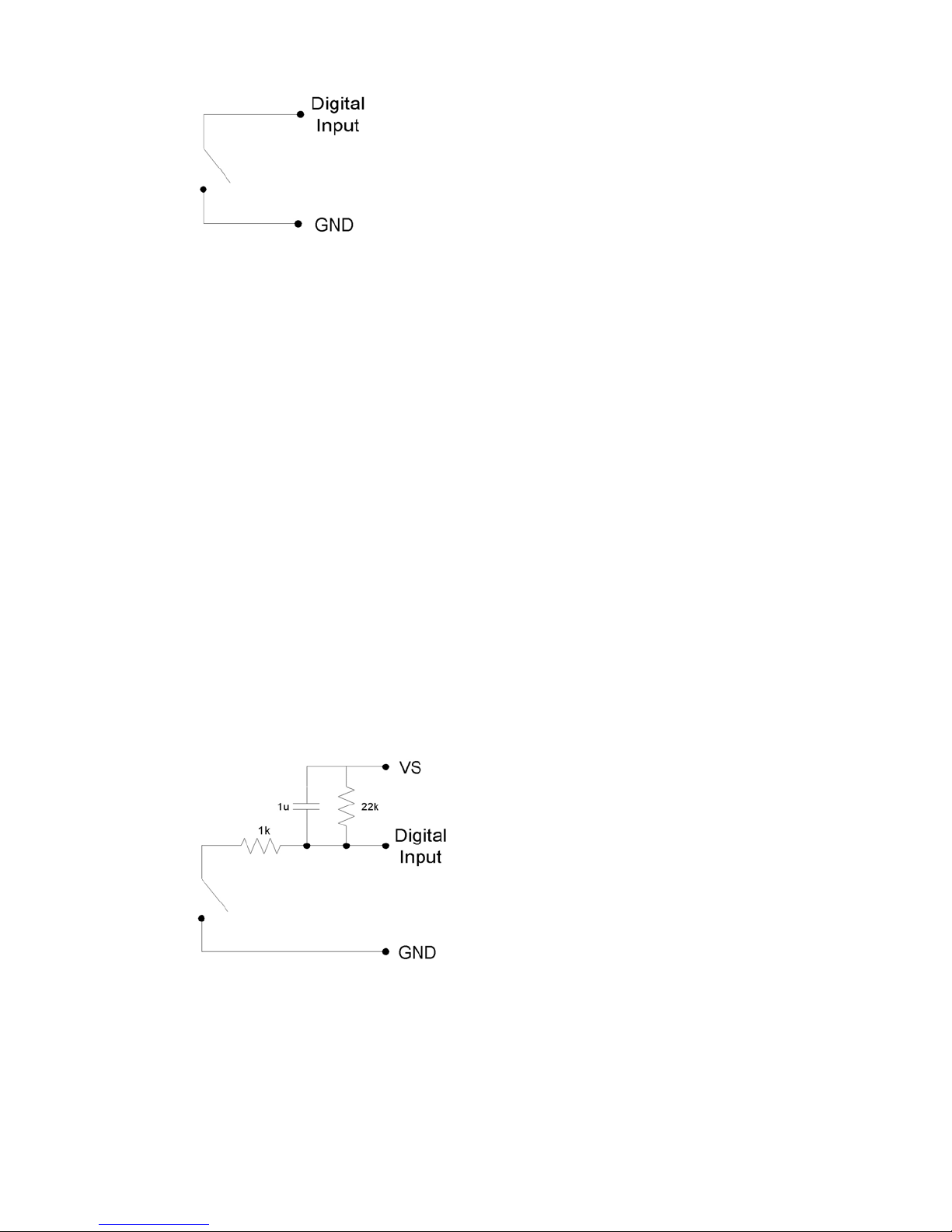
Figure 2-10. Basic Mechanical Switch Connection To Digital Input
When the switch is open, the internal 100 kΩ pull-up resistor will pull the digital input to about
3.3 volts (logic high). When the switch is closed, the ground connection will overpower the pullup resistor and pull the digital input to 0 volts (logic low). Since the mechanical switch does not
have any electrical connections, besides to the LabJack, it can safely be connected directly to
GND, without using a series resistor or SGND.
When the mechanical switch is closed (and even perhaps when opened), it will bounce briefly
and produce multiple electrical edges rather than a single high/low transition. For many basic
digital input applications, this is not a problem as the software can simply poll the input a few
times in succession to make sure the measured state is the steady state and not a bounce. Fo
applications using timers or counters, however,
c
ounters, for instance, are very fast and will increment on all the bounces. Some solutions to
this usually is a problem. The hardware
this issue are:
• Software Debounce: If it is known that a real closure cannot occur more than once pe
r
some interval, then software can be used to limit the number of counts to that rate.
• Firmware Debounce: See section 2.10.1 for information about timer mode 6.
• Active Hardware Debounce: Integrated circuits are available to debounce switch
signals.
This is the most reliable hardware solution. See the MAX6816 (maxim-ic.com)
or EDE2008 (elabinc.com).
• Passive Hardware Debounce: A combination of resistors and capacitors can be used to
debounce a signal. This is not foolproof, but works fine in most applications.
r
Figure 2-11. Passive Hardware Debounce
Figure 2-12 shows one possible configuration for passive hardware debounce. First, consider
the case where the 1 kΩ resistor is replaced by a short circuit. When the switch closes it
immediately charges the capacitor and the digital input sees logic low, but when the switch
opens the capacitor slowly discharges through the 22 kΩ resistor with a time constant of 22 ms.
By the time the capacitor has discharged e
mechanical bouncing is done. The main p
28
ough for the digital input to see logic high, the
n
urpose of the 1 kΩ resistor is to limit the current surge
Page 29
when the switch is closed. 1 kΩ limits the maximum current to about 5 mA, but better results
might be obtained with smaller resistor values.
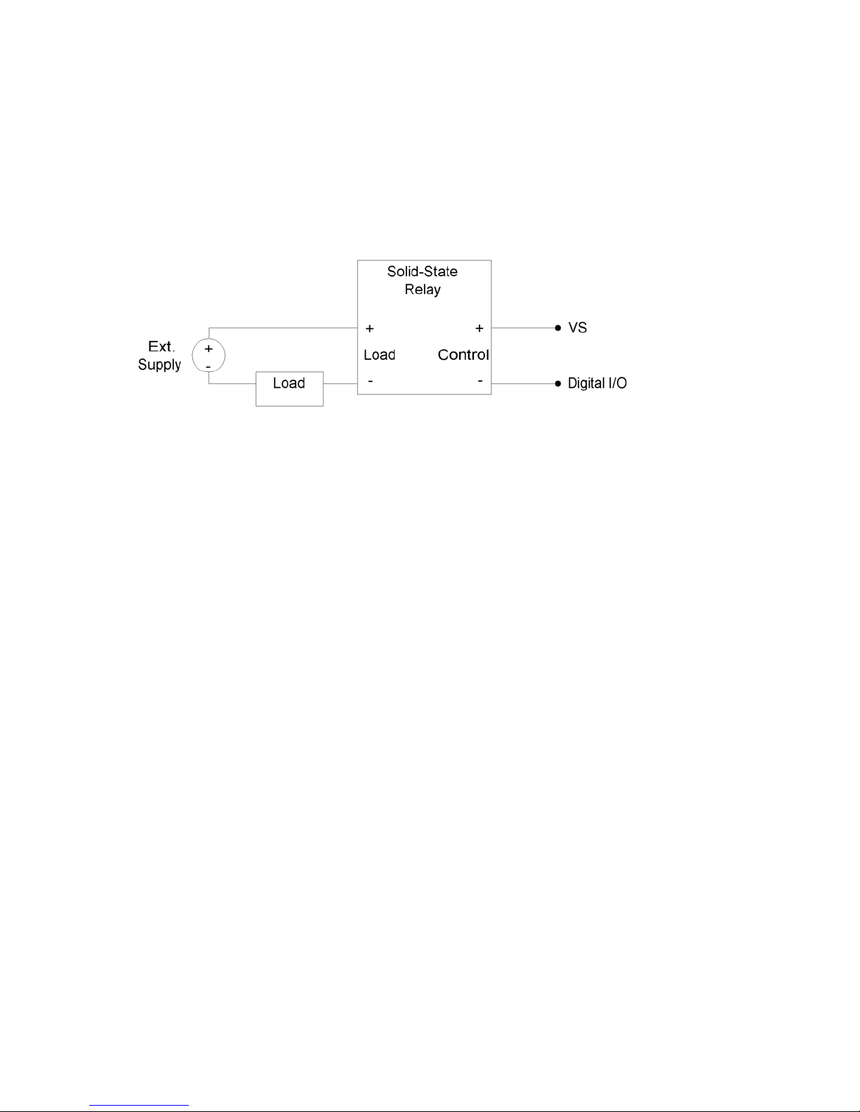
2.8.1.4 Output: Controlling Relays
All the digital I/O lines have series resistance that restricts the amount of current they can s
or source, but solid-state relays (SSRs) can usually be controlled directly by the digital I/O. The
SSR is connected as shown in the following diagram, where VS (~5 volts) connects to the
positive control input and the digital I/O line con
c
onfiguration).
nects to the negative control input (sinking
Figure 2-12. Relay Connections (Sinking Control, High-Side Load Switching)
When the digital line is set to output-low, control current flows and the relay turns on. When the
digital line is set to input, control current does not flow and the relay turns off. When the digital
line is set to output-high, some current flows, but whether the relay is on or off depends on the
specifications of a particular relay. It is recommended to only use output-low and input.
F
or example, the Series 1 (D12/D24) or Series T (TD12/TD24) relays from Crydom specify a
max turn-on of 3.0 volts, a min turn-off of 1.0 volts, and a nominal input impedance of 1500 Ω.
• When the digital line is set to output-low, it is the equivalent of a ground connection with
180 Ω (EIO/CIO) or 550 Ω (FIO) in series. When using an EIO/CIO/MIO line, the
resulting voltage across the control inputs of the relay will be about 5*1500/(1500+180) =
4.5 volts (the other 0.5 volts is dropped across the internal resistance of the EIO/CIO
line). With an FIO line the voltage across the inputs of the relay will be about
5*1500/(1500+550) = 3.7 volts (the other 1.3 volts are dropped across the internal
resistance of the FIO line). Both of these are well above the 3.0 volt threshold for the
relay, so it will turn on.
When the digital line is set to input, it is the equivalent of a 3.3 volt connection with 10
• 0
kΩ in series. The resulting voltage across the control inputs of the relay will be
zero, as virtually all of the 1.7 volt difference (between VS and 3.3) is dropped acro
internal 100 kΩ resistance. This is well below the 1.0 volt threshold for the relay, so it
will turn off.
• When the digital line is set to output-high, it is the equivalent of a 3.3 volt connection with
180 Ω (EIO/CIO) or 550 Ω (FIO) in series. When using an EIO/CIO line, the resulting
voltage across the control inputs of the relay will be about 1.7*1500/(1500+180) = 1.5
volts. With an FIO line the voltage across the inputs of the relay will be about
1.7*1500/(15
00+550) = 1.2 volts. Both of these in the 1.0-3.0 volt region that is not
defined for these example relays, so the resulting state is unknown.
ink
close to
ss the
29
Page 30

Mecha y
the dig uffer is
used. or
an op-a
N
mechanical relays, and thus can be a convenient way to control 1 or 2 relays.
The RB12 relay board is a useful accessory available from LabJack. This board connects to the
DB15 conne
O
Another accessory available from LabJack is the LJTick-RelayDriver. This is a
m
50 volts and sink up to 200 mA. This allows control of virtually any solid-state or mechanical
relay.
2
The U3 has 2 timers (Timer0-Timer1) and 2 counters (Counter0-Counter1). When any of these
timers or counters are enabled, they take over an FIO/EIO line in sequence (Timer0, Timer1,
Counter0, then Counter1), starting with FIO0+TimerCounterPinOffset. Some examples:
1 Timer enabled, Counter0 dis
FIO0=Timer0
1 Timer enabled, Counter0 disabled, Counter1 enabled, and TimerCounterPinOffset=2:
FIO2=Timer0
FIO3=Counter1
2 Timers enab
E
EIO1=Timer1
EIO2=Counter
EIO3=Counter1
Timers and counters can appear on various pins, but other I/O lines never move. For exa
Timer1 can ap
whether Timer
terminal labeled F
N
does not use an external FIO/EIO pin. Counter0 does not use an external An error will result if
an attempt is made to enable Counter0 when one of these frequencies are configured.
Similarly, an error will result if an attempt is made to configure one of these frequencies when
Counter0 is enabled.
Applicable digital I/O are automatically configured as input or output as needed when timers and
counters are enabled, and stay that way when the timers/counters are disabled.
See Section 2.8.1 for information about signal connections.
nical relays require more control current than SSRs, and cannot be controlled directly b
ital I/O on the U3. To control higher currents with the digital I/O, some sort of b
Some options are a discrete transistor (e.g. 2N2222), a specific chip (e.g. ULN2003),
mp.
ote that the U3 DACs can source enough current to control almost any SSR and even some
ctor on the U3 and accepts up to 12 industry standard I/O modules (designed for
pto22 G4 modules and similar).
two channel
odule that plugs into the U3 screw-terminals, and allows two digital lines to each hold off up to
.9 Timers/Counters
abled, Counter1 disabled, and TimerCounterPinOffset=0:
led, Counter0 enabled, Counter1 enabled, and TimerCounterPinOffset=8:
IO0=Timer0
0
mple,
pear anywhere from FIO0 to EIO1, depending on TimerCounterPinOffset and
0 is enabled. On the other hand, FIO5 (for example), is always on the screw
IO5, and AIN5 (if enabled) is always on that same screw terminal.
ote that Counter0 is not available with certain timer clock base frequencies. In such a case, it
30
Page 31

Each counter (Counter0 or Counter1) consists of a 32-bit register that accumulates the number
of falling edges detected on the external pin. If a counter is reset and read in the
c
all, the read returns the value just before the reset.
same function
T
he timers (Timer0-Timer1) have various modes available:
Timer Modes
0 16-bit PWM output
1 8-bit PWM output
2 Period input (32-bit, rising edges)
3 Period input (32-bit, falling edges)
4 Duty cycle input
5 Firmware counter input
6 Firmware counter input (with debounce)
7 Frequency output
8 Quadrature input
9 Timer stop input (odd timers only)
10
11 System timer high read
12 Period input (16-bit, rising edges)
13 Period input (16-bit, falling edges)
System timer low read
(default mode)
Both timers use the same timer clock. There are 7 choices
for the timer base clock:
TimerBaseClock
04 MHz
112 MHz
2 48 MHz (Default)
3 1 MHz /Divisor
4 4 MHz /Divisor
5 12 MHz /Divisor
6 48 MHz /Divisor
Note that these clocks a
pply to the U3 hardware revision 1.21. With hardware revision 1.20 all
clocks are half of the values above.
The first 3 clocks have a
frequency of the last 4 clocks ca
th
ese clocks Counter0 is not available. When Counter0 is not available, it does not use an
fixed frequency, and are not affected by TimerClockDivisor. The
n be further adjusted by TimerClockDivisor, but when using
external FIO/EIO pin.
N
ote that the DACs (Section 2.x) are derived from PWM signals that are affected by the timer
clock frequency. The default timer clock frequency of the U3 is set to 48 MHz, as this resul
the minimum DAC output noise. If the frequency is lowered, the DACs will have more noise,
where the frequency of the noise is the timer clock frequency divided by 2
8
.
ts in
31
Page 32

2.9.1 Timer Mode Descriptions
2.9.1.1 PWM Output (16-Bit, Mode 0)
Outputs a pulse width modulated rectangular wave output. Value passed should be 0-65535,
and determines what portion of the total time is spent low (out of 65536 total increments). That
means the duty cycle can be varied from 100% (0 out of 65536 are low) to 0.0015% (65535 out
of 65536 are low).
The overall frequency of the PWM output is the clock frequency specified by
TimerClockBase/TimerClockDivisor divided by 2
available PWM frequencies based on timer clock settings.
PWM16 Frequency Ranges
TimerBaseClock Divisor=1 Divisor=256
0 4 MHz 61.04 N/A
1 12 MHz 183.11 N/A
2 48 MHz (Default) 732.42 N/A
3 1 MHz /Divisor 15.26 0.060
4 4 MHz /Divisor 61.04 0.238
5 12 MHz /Divisor 183.11 0.715
6 48 MHz /Divisor 732.42 2.861
Note that the clocks above apply to the U3 hardware revision 1.21. With hardware revision 1.20
all clocks are half of those values.
The same clock applies to all timers, so all 16-bit PWM channels will have the same frequency
and will have their falling edges at the same time.
PWM output starts by setting the digital line to output-low for the specified amount of time. The
output does not necessarily start instantly, but rather waits for the internal clock to roll. For
example, if the PWM frequency is 100 Hz, that means the period is 10 milliseconds, and thus
after the command is received by the device it could be anywhere from 0 to 10 milliseconds
before the start of the PWM output.
2.9.1.2 PWM Output (8-Bit, Mode 1)
Outputs a pulse width modulated rectangular wave output. Value passed should be 0-65535,
and determines what portion of the total time is spent low (out of 65536 total increments). The
lower byte is actually ignored since this is 8-bit PWM. That means the duty cycle can be varied
from 100% (0 out of 65536 are low) to 0.4% (65280 out of 65536 are low).
The overall frequency of the PWM output is the clock frequency specified by
TimerClockBase/TimerClockDivisor divided by 2
available PWM frequencies based on timer clock settings.
PWM8 Frequency Ranges
TimerBaseClock Divisor=1 Divisor=256
0 4 MHz 15625.00 N/A
1 12 MHz 46875.00 N/A
2 48 MHz (Default) 187500.00 N/A
3 1 MHz /Divisor 3906.25 15.259
4 4 MHz /Divisor 15625.00 61.035
5 12 MHz /Divisor 46875.00 183.105
6 48 MHz /Divisor 187500.00 732.422
32
16
. The following table shows the range of
8
. The following table shows the range of
Page 33

Note that the clocks above apply to the U3 hardware revision 1.21. With hardware revision 1.20
all clocks are half of those values.
The same clock applies to all timers, so all 8-bit PWM channels will have the same frequency
and will have their falling edges at the same time.
PWM output starts by setting the digital line to output-low for the specified amount of time. The
output does not necessarily start instantly, but rather waits for the internal clock to roll. For
example, if the PWM frequency is 100 Hz, that means the period is 10 milliseconds, and thus
after the command is received by the device it could be anywhere from 0 to 10 milliseconds
before the start of the PWM output.
2.9.1.3 Period Measurement (32-Bit, Modes 2 & 3)
Mode 2: On every rising edge seen by the external pin, this mode records the number of clock
cycles (clock frequency determined by TimerClockBase/TimerClockDivisor) between this rising
edge and the previous rising edge. The value is updated on every rising edge, so a read
returns the time between the most recent pair of rising edges.
In this 32-bit mode, the processor must jump to an interrupt service routine to record the time,
so small errors can occur if another interrupt is already in progress. The possible error sources
are:
• Other edge interrupt timer modes (2/3/4/5/8/9/12/13). If an interrupt is already being
handled due to an edge on the other timer, delays of a few microseconds are possible.
• If a stream is in progress, every sample is acquired in a high-priority interrupt. These
interrupts could cause delays on the order of 10 microseconds.
• The always active U3 system timer causes an interrupt 61 times per second. If this
interrupt happens to be in progress when the edge occurs, a delay of about 1
microsecond is possible. If the software watchdog is enabled, the system timer interrupt
takes longer to execute and a delay of a few microseconds is possible.
Note that the minimum measurable period is limited by the edge rate limit discussed in Section
2.9.2.
Writing a value of zero to the timer performs a reset. After reset, a read of the timer value will
return zero until a new edge is detected. If a timer is reset and read in the same function call,
the read returns the value just before the reset.
Mode 3 is the same except that falling edges are used instead of rising edges.
2.9.1.4 Duty Cycle Measurement (Mode 4)
Records the high and low time of a signal on the external pin, which provides the duty cycle,
pulse width, and period of the signal. Returns 4 bytes, where the first two bytes (least
significant word or LSW) are a 16-bit value representing the number of clock ticks during the
high signal, and the second two bytes (most significant word or MSW) are a 16-bit value
representing the number of clock ticks during the low signal. The clock frequency is determined
by TimerClockBase/TimerClockDivisor.
The appropriate value is updated on every edge, so a read returns the most recent high/low
times. Note that a duty cycle of 0% or 100% does not have any edges.
To select a clock frequency, consider the longest expected high or low time, and set the clock
frequency such that the 16-bit registers will not overflow.
33
Page 34

Note that the minimum measurable high/low time is limited by the edge rate limit discussed in
Section 2.9.2.
When using the LabJackUD driver the value returned is the entire 32-bit value. To determine
the high and low time this value should be split into a high and low word. One way to do this is
to do a modulus divide by 2
16
to determine the LSW, and a normal divide by 216 (keep the
quotient and discard the remainder) to determine the MSW.
Writing a value of zero to the timer performs a reset. After reset, a read of the timer value will
return zero until a new edge is detected. If a timer is reset and read in the same function call,
the read returns the value just before the reset. The duty cycle reset is special, in that if the
signal is low at the time of reset, the high-time/low-time registers are set to 0/65535, but if the
signal is high at the time of reset, the high-time/low-time registers are set to 65535/0. Thus if no
edges occur before the next read, it is possible to tell if the duty cycle is 0% or 100%.
2.9.1.5 Firmware Counter Input (Mode 5)
On every rising edge seen by the external pin, this mode increments a 32-bit register. Unlike
the pure hardware counters, these timer counters require that the firmware jump to an interrupt
service routine on each edge.
Writing a value of zero to the timer performs a reset. After reset, a read of the timer value will
return zero until a new edge is detected. If a timer is reset and read in the same function call,
the read returns the value just before the reset.
2.9.1.6 Firmware Counter Input With Debounce (Mode 6)
Intended for frequencies less than 10 Hz, this mode adds a debounce feature to the firmware
counter, which is particularly useful for signals from mechanical switches. On every applicable
edge seen by the external pin, this mode increments a 32-bit register. Unlike the pure hardware
counters, these timer counters require that the firmware jump to an interrupt service routine on
each edge.
When configuring only (UpdateConfig=1), the low byte of the timer value is a number from 0255 that specifies the debounce period in ~30 ms intervals. In the high byte of the timer value,
bit 0 determines whether negative edges (bit 0 clear) or positive edges (bit 0 set) are counted.
Assume this mode is enabled with a value of 1, meaning that the debounce period is 30 ms and
negative edges will be counted. When the input detects a negative edge, it increments the
count by 1, and then waits 30 ms before re-arming the edge detector. Any negative edges
within the 30 ms debounce period are ignored. This is good behavior for a normally-high signal
where the switch closure causes a brief low signal (Figure 2-9). The debounce period can be
set long enough so that bouncing on both the switch closure and switch open is ignored.
When only updating and not configuring, writing a value of zero to the timer performs a reset.
After reset, a read of the timer value will return zero until a new edge is detected. If a timer is
reset and read in the same function call, the read returns the value just before the reset.
2.9.1.7 Frequency Output (Mode 7)
Outputs a square wave at a frequency determined by TimerClockBase/TimerClockDivisor
divided by 2*Timer#Value. The Value passed should be between 0-255, where 0 is a divisor of
256. By changing the clock configuration and timer value, a wide range of frequencies can be
output, as shown in the following table:
34
Page 35

Mode 7 Frequency Ranges
Divisor=1 Divisor=1
TimerBaseClock
0 4 MHz 2000000.0 7812.50
1 12 MHz 6000000.0 23437.50
2 48 MHz (Default) 24000000.0 93750.00
3 1 MHz /Divisor 500000.0 7.629
4 4 MHz /Divisor 2000000.0 30.518
5 12 MHz /Divisor 6000000.0 91.553
6 48 MHz /Divisor 24000000.0 366.211
Value=1 Value=256
Divisor=1 Divisor=256
Value=1
Value=256
Note that the clocks above apply to the U3 hardware revision 1.21. With hardware revision 1.20
all clocks are half of those values.
The frequency output has a -3 dB frequency of about 10 MHz on the FIO lines. Accordingly, at
high frequencies the output waveform will get less square and the amplitude will decrease.
The output does not necessarily start instantly, but rather waits for the internal clock to roll. For
example, if the output frequency is 100 Hz, that means the period is 10 milliseconds, and thus
after the command is received by the device it could be anywhere from 0 to 10 milliseconds
before the start of the frequency output.
2.9.1.8 Quadrature Input (Mode 8)
Requires both timers, where Timer0 will be quadrature channel A, and Timer1 will be
quadrature channel B. Timer#Value passed has no effect. The U3 does 4x quadrature
counting, and returns the current count as a signed 32-bit integer (2’s complement). The same
current count is returned on both timer value parameters.
Writing a value of zero to either or both timers performs a reset of both. After reset, a read of
either timer value will return zero until a new quadrature count is detected. If a timer is reset
and read in the same function call, the read returns the value just before the reset.
2.9.1.9 Timer Stop Input (Mode 9)
This mode should only be assigned Timer1. On every rising edge seen by the external pin, this
mode increments an 8-bit register. When that register matches the specified timer value (stop
count value), Timer0 is stopped. The range for the stop count value is 1-65535. Generally, the
signal applied to Timer1 is from Timer0, which is configured as output. One place where this
might be useful is for stepper motors, allowing control over a certain number of steps.
Once this timer reaches the specified stop count value, and stops the adjacent timer, the timers
must be reconfigured to restart the output.
When Timer0 is stopped, it is still enabled but just not outputting anything. Thus rather than
returning to whatever previous digital I/O state it had, it goes to input (which has a 100 kΩ pullup). That means the best results are obtained if Timer0 was initially configured as input (factory
default), rather than output-high or output-low.
The read from this timer mode returns the number of edges counted, but does not increment
past the stop count value.
35
Page 36

2.9.1.10 System Timer Low/High Read (Modes 10 & 11)
The LabJack U3 has a free-running internal 64-bit system timer with a frequency of 4 Mz. Timer
modes 10 & 11 return the lower or upper 32-bits of this timer. An FIO line is allocated for these
modes like normal, even though they are internal readings and do not require any external
connections. This system timer cannot be reset, and is not affected by the timer clock.
If using both modes 10 & 11, read both in the same low-level command and read 10 before 11.
2.9.1.11 Period Measurement (16-Bit, Modes 12 & 13)
Similar to the 32-bit edge-to-edge timing modes described above (modes 2 & 3), except that
hardware capture registers are used to record the edge times. This limits the times to 16-bit
values, but is accurate to the resolution of the clock, and not subject to any errors due to
firmware processing delays.
Note that the minimum measurable period is limited by the edge rate limit discussed in Section
2.9.2.
2.9.2 Timer Operation/Performance Notes
Note that the specified timer clock frequency is the same for all timers. That is, TimerClockBase
and TimerClockDivisor are singular values that apply to all timers. Modes 0, 1, 2, 3, 4, 7, 12,
and 13, all are affected by the clock frequency, and thus the simultaneous use of these modes
has limited flexibility. This is often not an issue for modes 2 and 3 since they use 32-bit
registers.
The output timer modes (0, 1, and 7) are handled totally by hardware. Once started, no
processing resources are used and other U3 operations do not affect the output.
The edge-detecting timer input modes do require U3 processing resources, as an interrupt is
required to handle each edge. Timer modes 2, 3, 5, 9, 12, and 13 must process every
applicable edge (rising or falling). Timer modes 4 and 8 must process every edge (rising and
falling). To avoid missing counts, keep the total number of processed edges (all timers) less
than 30,000 per second (hardware V1.21). That means that in the case of a single timer, there
should be no more than 1 edge per 33 μs. For multiple timers, all can process an edge
simultaneously, but if for instance both timers get an edge at the same time, 66 μs should be
allowed before any further edges are applied. If streaming is occurring at the same time, the
maximum edge rate will be less (7,000 per second), and since each edge requires processing
time the sustainable stream rates can also be reduced.
2.10 SCL and SDA (or SCA)
Reserved for future use.
2.11 DB15
The DB15 connector brings out 12 additional digital I/O. It has the potential to be used as an
expansion bus, where the 8 EIO are data lines and the 4 CIO are control lines.
In the Windows LabJackUD driver, the EIO are addressed as digital I/O bits 8 through 15, and
the CIO are addressed as bits 16-19.
36
Page 37

0-7 FIO0-FIO7
8-15 EIO0-EIO7
16-19 CIO0-CIO3
These 12 channels include an internal series resistor that provides overvoltage/short-circuit
protection. These series resistors also limit the ability of these lines to sink or source current.
Refer to the specifications in Appendix A.
All digital I/O on the U3 have 3 possible states: input, output-high, or output-low. Each bit of I/O
can be configured individually. When configured as an input, a bit has a ~100 kΩ pull-up
resistor to 3.3 volts. When configured as output-high, a bit is connected to the internal 3.3 volt
supply (through a series resistor). When configured as output-low, a bit is connected to GND
(through a series resistor).
DB15 Pinouts
1Vs 9CIO0
2CIO1 10CIO2
3CIO3 11GND
4EIO0 12EIO1
5EIO2 13EIO3
6EIO4 14EIO5
7EIO6 15EIO7
8GND
2.11.1 CB15 Terminal Board
The CB15 terminal board connects to the LabJack U3’s DB15 connector. It provides convenient
screw terminal access to the 12 digital I/O available on the DB15 connector. The CB15 is
designed to connect directly to the LabJack, or can connect via a standard 15-line 1:1 malefemale DB15 cable.
2.11.2 RB12 Relay Board
The RB12 provides a convenient interface for the U3 to industry standard digital I/O modules,
allowing electricians, engineers, and other qualified individuals, to interface a LabJack with high
voltages/currents. The RB12 relay board connects to the DB15 connector on the LabJack, using
the 12 EIO/CIO lines to control up to 12 I/O modules. Output or input types of digital I/O
modules can be used. The RB12 is designed to accept G4 series digital I/O modules from
Opto22, and compatible modules from other manufacturers such as the G5 series from Grayhill.
Output modules are available with voltage ratings up to 200 VDC or 280 VAC, and current
ratings up to 3.5 amps.
37
Page 38

2.12 U3-OEM
There is an OEM version of the U3 available. It is a board only (no enclosure), and does not
have most of the through-hole components installed. The picture below shows how the U3OEM ships by default. Leaving the through-hole parts off makes the OEM board very flexible.
Many applications do not need the through-hole parts, but if needed they are much easier to
install than uninstall.
In the picture, note the holes available for 0.1" pin-header connectors. Connectors J3 & J4
provide pin-header access to the connections that would normally appear on the left and right
screw-terminals. Connector J2 provides a pin-header alternative to the DB15 connector. The
idea is that an OEM can connect ribbon cables to the pin-headers, or even plug the U3 directly
to the customers main board designed with mating pin-header receptacles.
J2
1GND 2VS
3CIO0 4CIO1
5CIO2 6CIO3
7GND 8EIO0
9 EIO1 10 EIO2
11 EIO3 12 EIO4
13 EIO5 14 EIO6
15 EIO7 16 GND
J3
1FIO4 2FIO5
3FIO6 4FIO7
5VS 6GND
7SDA 8SCL
9VS 10GND
J4
1FIO0 2FIO1
3FIO2 4FIO3
5VS 6GND
7DAC0 8DAC1
9VS 10GND
38
Page 39

2.13 Hardware Revision Notes
Starting September of 2006, all U3 shipments changed from hardware revision 1.20 to 1.21.
Following are the some of the main changes in revision 1.21:
• The default timer clock frequency is 48 MHz.
• All TimerBaseClock frequencies are twice the previous frequencies.
• The input timer edge limit is now 30,000 edges/second, compared to the old limit of
10,000 edges/second.
• Stream mode is now supported. See Section 3.2.
• Other new functions are supported, including Watchdog, SPI, Asynch, I2C, and SHT1X.
• Typical supply current is 50 mA.
Older U3s can be upgraded by LabJack for a small fee. For information about upgrading a rev
1.20 unit, go to labjack.com.
39
Page 40

3. Operation
3.1 Command/Response
Eve th mode, meaning that all
ry ing besides streaming is done in command/response
com u
m nication is initiated by a command from the ho
U3.
the
For eve figuration, the low-level Feedback function is the primary function
use a Windows UD driver uses the
Fee a
stre
rything besides pin con
d, s it writes and reads virtually all I/O on the U3. The
db ck function under-the-hood to handle most requests besides configuration and
aming.
The following tables show typical measured execution times for command/response mode. The
time varies primarily with the
number of analog inputs requested, and is not noticeably affected
by the number of digital I/O, DAC, timer, and counter operations.
These times were measured using the example program “allio.c” (VC6_LJUD). The program
executes a loop 1000 times and divides the total time by 1000, and thus include everything
(Windows latency, UD driver overhead, communication time, U3 processing time, etc.).
USB high-high USB other
# AIN
0
1
4
8
16
[milliseconds] [milliseconds]
0.6 4.0 <- Write/Read all DIO, DACs, Timers & Counters
0.8 4.0
2.2 4.0
4.1 5.2
8.2 12.4
st which is followed by a response from
Table 3-1. Typical Feedback Function Execution Times (QuickSample=0, LongSettling=0)
USB high-high USB other
# AIN
0
1
4
8
16
Table 3-2. Typical Feedback Function Execution Times (QuickSample=1, LongSettling=0)
[milliseconds] [milliseconds]
0.6 4.0 <- Write/Read all DIO, DACs, Timers & Counters
0.6 4.0
0.9 4.0
1.5 4.0
3.0 8.0
USB high-high USB other
# AIN
0
1
4
8
16
Table 3-3. Typical Feedback Function Execution Times (QuickSample=0, LongSettling=1)
[milliseconds] [milliseconds]
0.6 4.0 <- Write/Read all DIO, DACs, Timers & Counters
4.2 5.2
16 17
32 33
63 65
40
Page 41

A “USB high-high” con
then connected to a high-speed US
device, such a configuration does p
figuration means the U3 is connected to a high-speed USB2 hub which is
B2 host. Even though the U3 is not a high-speed USB
rovide improved performance.
The analog inputs have a QuickSample option where each conversion is done faster at the
expense o
c
hannel
f increased noise. This is enabled by passing a nonzero value for put_config special
LJ_chAIN_RESOLUTION. There is also a LongSettling option where additional settling
time is added between the internal mulitplexer configuration and the analog to digital
conversion. This allows signals with more source impedance, and is enabled by passing
nonzero value for put_config special channel
are disabled
by default, so the first table above shows the default conditions.
LJ_chAIN_SETTLING_TIME. Both of these o
a
ptions
The first row in each of the above tables (# AIN = 0) includes a write and read to all I/O on the
U3 besides analog inputs (digital I/O, DAC0, timers, and counters).
T
he tables above were measured with U3 hardware version 1.21 which started shipping in late
August of 2006. The times could be up to twice as long with hardware version 1.20 or less.
41
Page 42

3.2 Stream Mode
The highest input data rates are obtained in stream mode, which is supported with U3 hardware
version 1.21 or higher. Hardware version 1.21 started shipping in late August of 2006. Con
abJack for information about upgrading older U3s. Stream is a co
L
ntinuous hardware timed
input mode where a list of channels is scanned at a specified scan rate. The scan rate spec
the interval between the beginning of each scan. The samples within each scan are acquired
as fast as possible.
As samples are collected, they are placed in a small FIFO buffer on the U3, until retrieved by
the host. The buffer typically holds 984 samples, but the size ranges from 512 to 984
depending on the number of samples per packet. Each data packet has various measures to
e
nsure the integrity and completeness of the data received by the host.
Since the data buffer on the U3 is very small it uses a feature called auto-recovery. If the buffe
overflows, the U3 will continue streaming but discard data until the bu
ffer is emptied, and then
data will be stored in the buffer again. The U3 keeps track of how many packets are discarded
and reports that value. Based on the number of packets discarded, the UD driver adds the
proper number of dummy samples (-9999.0) such that the correct timing is maintained.
The table below shows various stream performance parameters. Some systems might require
a USB high-high configuration to obtain the maximum speed in the last row of the table. A “USB
high-high” configuration means the U3 is connected to a high-speed USB2 hub which is then
connected to a high-speed USB2 host. Even though the U3 is not a high-speed USB device,
such a configuration does often provide improved performance.
Stream data rates over USB can also be limited by other factors such as speed of the PC and
program design. One general technique for robust continuous streaming would be increasing
the priority of the stream process.
A sample is defined as a single conversion of a single channel, while a scan is defined as a
single conversion of all channels being acquired. That means the maximum scan rate for a
stream of five channels is 50k/5 = 10 kscans/second.
tact
ifies
r
Low-Level UD Max Stream ENOB ENOB Noise Interchannel
Res Index
0 100
1 101
2 102
3 103
Table 3-4. Stream Performance
Res Index (Samples/s) (RMS) (Noise-Free) (Counts)
Full resolution streaming is limited to 2500 samples/s, but higher speeds are possible at the
expense of reduced effective resolution (increased noise). The first column above is the index
passed in the Resolution parameter to the low-level StreamConfig function, while the second
column is the corresponding index for the Resolution parameter in the UD driver. In the UD
driver, the default Resolution index is 0, which corresponds to automatic selection. In this case,
the driver will use the highest resolution for the specified sample rate.
ENOB stands for effective number of bits. The first ENOB column is the commonly used
“effective” resolution, and can be thought of as the resolution obtained by most readings. This
42
2500
10000
20000
50000
12.8
11.9
11.3
10.5
Delay (μs)
10.0 ±2 320
9.0 ±4 82
8.4 ±6 42
7.5 ±11 12.5
Page 43

data is calculated by collecting 128 samples and evaluating the standard deviation (RMS noise).
The second ENOB colum
n is the noise-free resolution, and is the resolution obtained by all
readings. This data is calculated by collecting 128 samples and evaluating the maximum value
minus the minimum value (peak-to-peak noise). Similarly, the Noise Counts column is the
peak-to-peak noise based on counts from a 12-bit reading.
Interchannel delay is the time between successive channels within a stream scan.
3.2.1 Streaming Digital Inputs, Timers, and Counter0
There are special channel numbers that allow digital inputs, timers, and counters, to be
streamed in with analog input data.
Channel#
193 EIO_FIO
200 Timer0
201 Timer1
210 Counter0
211 Counter1
224 TC_Capture
Table 3-5. Special Stream Channels
Channel number 193 returns the input states of 16 bits of digital I/O. FIO is the lower 8 bits an
EIO is the upper 8 bits.
Channels 200-201 and 210-211 retrieve the least significant word (LSW, lower 2 bytes) of the
specified timer/counter. At the same time, the most significant word (MSW, upper 2 bytes) is
stored in an internal timer/counter capture register (TC_Capture), so that the proper value can
b
e sampled later in the scan.
Adding these special channels to the stream scan list does not configure those inputs. If any
the FIO or EIO lines have been configured as outputs, timers, counter, or analog inputs, a
hannel 193 read will still be performed without error b
c
nored. The timers/counters (200-224) must be configured before streaming using normal
ig
ut the values from those bits should be
timer/counter configuration commands.
The timing for these special channels is the same as for normal analog channels. For instance,
a stream of the scan list {0,1,200,224,201,224} counts as 6 channels, and the maximum scan
rate is determined by taking the maximum sample rate at the specified resolution and dividing
by 6.
Special care must be taken whe
m
easurement). It is possible for the LSW to roll, but the MSW be captured before it is
n streaming timers configured in mode 2 or 3 (32-bit period
incremented. If this is an unacceptable situation, then only the LSW or MSW should be used
but not both.
d
of
,
43
Page 44

4. LabJackUD High-Level Driver
The low-level U3 functions are described in Section 5, but most Windows applications will use
the LabJackUD driver instead.
The driver requires a PC running Windows 98, ME, 2000, or XP. It is recommende
e software before making a USB connection to a LabJack.
th
The download version of the installer consists of a single executable
driver (LabJackUD.dll) in the Windows System directory, along with
. This installer places the
a support DLL
(LabJackUSB.dll). Generally this is c:\Windows\System\ on Windows 98/ME, and
c:\Windows\System32\ on Windows
2000/XP.
Other files, including the header and Visual C library file, are installed to the LabJack drivers
directory which defaults to c:\Program Files\LabJack\drivers\.
4.1 Overview
The general operation of the LabJackUD functions is as follows:
• Open a LabJack.
• Build a list of requests to perform (Add).
• Execute the list (Go).
• Read the result o
For example, to write an analog output and read an analog input:
//Use the following line to open the first found LabJack U3
//over USB and get a handle
/The general form of the o
/
//OpenLabJack (DeviceType, ConnectionType, Address, FirstFound, *Handle)
//Open the first found LabJack U3 over USB.
lngErrorcode = OpenLabJack (LJ_dtU3, LJ_ctUSB, "1", TRUE, &lngHandle);
//Request that DAC0 be set to 2.5 volts.
//The general form of the AddRequest
/AddRequest (Handle, IOType, Channel, Value, x1, UserData)
/
lngErrorcode = AddRequest (lngHandle, LJ_ioPUT_DAC, 0, 2.50, 0, 0);
//Request a read from AIN3 (FIO3), assuming it has been enabled as
//an analog line.
lngErr
//Execute the requests.
lngErrorcode = GoOne (lngHandle);
//Get the result of the DAC0 request just to check for an errorcode.
//The general
/
l
/
//voltage will be returned in that variable.
lngErrorcode = GetResult (lngHandle, LJ_ioGET_AIN, 3, &dblValue);
orcode = AddRequest (lngHandle, LJ_ioGET_AIN, 3, 0, 0, 0);
form of the GetResult function is:
/GetResult (Handle, IOType, Channel, *Value)
ngErrorcode = GetResult (lngHandle, LJ_ioPUT_DAC, 0, 0);
/Get the AIN3 voltage. We pass the address to dblValue and the
f each request (Get).
to the device.
pen function is:
function is:
d to install
44
Page 45

The AddRequest/Go/GetResult method is often the most efficient. As shown above, multiple
requests can be executed with a single Go() or GoO
optimize the requests into fewer low-level calls. The
ne() call, and the driver might be able to
other option is to use the eGet or ePut
functions which combine the AddRequest/Go/GetResult into one call. The above code would
t
hen look like (assuming the U3 i
s already open):
//Set DAC0 to 2.5 volts.
//The general form of the ePut function is:
/ePut (Handle, IOType, Channel, Value, x1)
/
lngErrorcode = ePut (lngHandle, LJ_ioPUT_DAC, 0, 2.50, 0);
//Read AIN3.
//The general form of the eGet function is:
//eGet (Handle, IOType, Channel, *Value, x1
ngErrorcode = eGet (lngHandle, LJ_ioGET_AI
l
)
N, 3, &dblValue, 0);
the case of the U3, the first example using add/go/get handles both th
In
AIN read in a single lowcommands are used
method and the ePu
level call, while in the second example using ePut/eGet two low-level
. Examples in the following documentation will use both the add/go/get
t/eGet method, and they are generally interchangeable. See Section 4.3 for
e DAC command and
more pseudocode examples.
the request and result
All functions always have 4 common parameters, and some of the
ctions have 2 extra parameters:
fun
• Handle – This is an input to all r
equest/result functions that tells the function
what LabJack it is talking to. The handle is obtained from the OpenLabJack
function.
• IOType – This is an input to all request/result functions that specifies what type
of action is being done.
• Channel – This is an input to all re
which channel of I/O is being written/read, although with the config
special constants are passed for cha
Value – This is an input or output to all request/result functions th
•
quest/result functions that generally specifies
IOTypes
nnel to specify what is being configured.
at is used to
write or read the value for the item being operated on.
• x1 – This parameter is only use
d in some of the request/result functions, and is
used when extra information is needed for certain IOTypes.
• UserData – This parameter is only used in some of the reque
st/result functions,
and is data that is simply passed along with the request, and returned unmodified
by the result. Can be used to store any sort of information w
allow a generic parser to determine what should be done when the result
ith the request, to
s are
received.
4.1.1 Function Flexibility
The driver is designed to be flexible so that it can work
different capabilities. It is also designed to work with
different capabilities. For this reason, many of the functions are r
parameters, although their internal functionality remains mostly the same
documentation, a group of functions will often be re
example, a reference to Add or AddRequest most likely refers to any of the
A
ddRequest(), AddRequestS() or AddRequestSS().
45
with various different LabJacks with
different development platforms with
epeated with different forms of
. In this
ferred to by their shortest name. For
three variations:
Page 46

In the sample code, alternate functions (S or SS versions) can generally be substituted as
desired, changing the parameter types accordingly. All samples here are written in pseudo-C
Functions with an “S” or “SS” appended are provided for programming languages that can’t
include the LabJackUD.h file and therefore can’t u
rogramming form to hardcode numbers into function calls, if for no other reason than it is hard
p
to read. Functions with a single “S” replace the IO
string. A string can then be passed with the name
double “SS” replace both the IOType and Channel with strings. O
D
eviceType and ConnectionType with strings since both take constants.
se the constants included. It is generally poor
Type parameter with a const char * which is a
of the desired constant. Functions with a
penLabJackS replaces both
For example:
C, where the LabJackUD.h file can be included and the constants used directly:
In
ddRequest(Handle, LJ_ioGET_CONFIG, LJ_ioHARDWARE_VERSION,0,0,0);
A
The bad way (hard to read) when LabJackUD.h cannot be included:
AddRequest(Handle, 1001, 10, 0, 0, 0);
The better way when LabJackUD.h cannot be included, is to pass strings:
AddRequestSS(Handle, “LJ_ioG
ET_CONFIG”, “LJ_ioHARDWARE_VERSION”,0,0,0);
Continuing on this vein, the function StringToConstant() is useful for error handling routine
with the GetFirst/Next functions whic
kes a string and returns the numeric constant. So, for example:
ta
h do not take strings. The StringToConstant() function
s, or
LJ_ERROR err;
err = AddRequestSS(Handle, “LJ_ioGETCONFIG”, “LJ_ioHARDWARE_VERSION”,0,0,0);
if (err == t
do some r
S ringToConstant(“LJE_INVALID_DEVICE_TYPE”))
er or handling..
Once agai h
if (err == 2)
n, t is is much clearer than:
.
4.1.2 Mu -
This driver is c these functions can
be called f
Because of thi
requests/resul
multiple thread
into another. I are added, and then results return LJE_NO_DATA_AVAILABLE or a
s
imilar error, chances are the requests and results are in different threads.
lti Threaded Operation
ompletely thread safe. With some very minor exceptions, all
rom multiple threads at the same time and the driver will keep everything straight.
s Add, Go, and Get must be called from the same thread for a particular set of
ts. Internally the list of requests and results are split by thread. This allows
s to be used to make requests without accidentally getting data from one thread
f requests
The driver tracks which thread a r
then a new one is created, it is possible for the new thread to have the same ID. Its not real
problem if Add is called first, but if Get is called on a new thread results could be returned fro
the thread that already ended.
As mentioned, the list of requests and results is kept on a thread-by-thread basis. Since t
driver cannot tell when a thread has ended, the results are kept in memory for that thread
regardless. This is not a problem in general as the driver will clean it all up when unloaded.
W
hen it can be a problem is in situations where thread
c
ontinuously. This will result in the slow consumption of memory as requests on old threads are
46
equest is made in by the thread ID. If a thread is killed and
ly a
m
he
s are created and destroyed
Page 47

left behind. Since each request only uses 44 bytes, and as mentioned the ID's will eventua
lly
get recycled, it will not be a huge memory loss. In general, even without this issue, it is strongly
commended to not create and destroy a lot of threads. It is terribly slow and inefficient. Use
re
thread pools and other techniques to keep new thread creation to a minimum. That is what i
s
done internally.
The one big exception to the thread safety of this driver is in the use of the Windows
TerminateThread() function. As is warned in the MSDN documentation, using
TerminateThread() will kill the thread without releasing any resources, and more importantly,
releasing any synchronization objects. If TerminateThread() is used on a thread that is currently
in
the middle of a call to this driver, more than likely a synchronization object will be left open on
the particular d
started. On some devices, it can be worse. On devices that have interprocess
re
synchronization, such as the U12, calling TerminateThread() may kill all access to t
through this driver no matter which process is using it and even if the application
A
void using TerminateThread()! All device calls have a timeout, which defaults to 1 second, but
can be changed. Make sure to wait at least as long as the timeout fo
evice and access to the device will be impossible until the application is
he device
is restarted.
r the driver to finish.
47
Page 48

4.2 Function Reference
The LabJack driver file is named LabJackUD.dll, and contains the functions described in this
section.
Some parameters are common to many functions:
• LJ_ERROR – A LabJack specific numeric error code. 0 means no error. (lon
32-bit integer).
• LJ_HANDLE – This value is returned by OpenLabJack, and then passed on to other
functions to identify the opened LabJack. (long, signed 32-bit integer).
To maintain compatibility with as many languages as possible, every attempt has been
keep the parameter types very basic. Also, many functions have multiple prototypes. The
declarations that follow, are written in C.
To help those unfamiliar with strings in C, these functions expect null terminated 8 bit ASCII
strings. How this translates to a particular development environment is beyond the scope
documentation. A const char * is a pointer to a string that won’t be changed by the driver.
Usually this means it can simply be a constant such as “this is a string”. A char * is a pointer to
a string that will be changed. Enough bytes must be preallocated to hold the possible strings
that will be returned. Functions with char * in their declaration will have the required length of
the buffer documented below.
Pointers must be initialized in general, although null (0) can be passed for unused or unneeded
values. The pointers for GetStreamData and RawIn/RawOut requests are not optional. Arrays
and char * type strings must be initialized to the proper size before passing to the DLL.
g, signed
made to
of this
4.2.1 ListAll()
Returns all the devices found of a given DeviceType and ConnectionType. Currently only USB
is supported.
ListAllS() is a special version where DeviceType and ConnectionType are strings rather than
longs. This is useful for passing string constants in languages that cannot include the header
file. The strings should contain the constant name as indicated in the header file (such as
“LJ_dtU3” and ”LJ_ctUSB”). The declaration for the S version of open is the same as below
except for (const char *pDeviceType, const char *pConnectionType, …).
Declaration:
LJ_ERROR _stdcall ListAll ( long DeviceType,
Parameter Description:
Returns: LabJack errorcodes or 0 for no error.
Inputs:
long ConnectionType,
long *pNumFound,
long *pSerialNumbers,
long *pIDs,
double *pAddresses)
• DeviceType – The type of LabJack to search for. Constants are in the
labjackud.h file.
48
Page 49

• ConnectionType – Enter the constant for the type of connection to use in the
search. Currently,
• pSerialNumbers – Must pass a pointer to a buffer with at least 128 elements.
• pIDs – Must pass a pointer to a buffer with at least 128 elements.
• pAddresses – Must pass a pointer to a buffer with at least 128 elements.
Outputs:
• pNumFound – Returns the number of devices found, and thus the number of
valid elements in the return arrays.
• pSerialNumbers – Array contains serial numbers of any found devices.
• pIDs – Array contains local IDs of any found devices.
• pAddresses – Array contains IP addresses of any found devices. The function
DoubleToStringAddress() is useful to convert these to string notation.
.2.2 OpenLabJack()
4
Call OpenLabJack() before communicating with a device. This function can be called multiple
times, however, once a LabJack is open, it remains open until your application ends (or the DLL
is unloaded). If OpenLabJack is called repeatedly with the same parameters, thus requesting
the same type of connection to the same LabJack, the driver will simply return the same
LJ_HANDLE every time. Internally, nothing else happens. This includes when the device is
reset, or disconnected. Once the device is reconnected, the driver will maintain the same
handle. If an open call is made
for each connection type and both connections will be open.
OpenLabJackS() is a special version of open where DeviceType and ConnectionType are
strings rather than longs. This is useful for passing string constants in languages that ca
clude the header file. The strings should contain the constant name as indicated in the header
in
file (such as “LJ_dtU3” and ”LJ_ctUSB”). The declaration for
as below except fo
Declaration:
LJ_ERROR _stdcall OpenLabJack ( long DeviceType,
Parameter De
Returns: LabJack errorcodes or 0 for no er
Inputs:
• DeviceType – to open. Constants are in the labjackud.h
• ConnectionTy he constant for the type of connection, USB or
• pAddress – For USB, pass the local ID or serial number of the desired LabJack.
• and ConnectionType parameters are
r (const char *pDeviceType, const char *pConnectionType, …).
scription:
file.
Ethernet.
For Ethernet pass the IP address of the desired LabJack. If FirstFound is true,
Address i
FirstFound – If true, then the Address
ignored and the driver opens the first LabJack found with the specified
DeviceType. Generally only recommended when a single LabJack is co
Currently only su
Ethernet but with the given Address.
s ignored.
only USB is supported for this function.
for USB, and then Ethernet, a different handle will be returned
nnot
the S version of open is the same
long ConnectionType,
const char *pAddress,
long FirstFound,
LJ_HANDLE *pHandle)
ror.
The type of LabJack
pe – Enter t
nnected.
pported with USB. If a USB device is not found, it will try
49
Page 50

Outputs:
pHandle – A pointer to a handle for a LabJack.
•
4.2.3 eG (
The eGet
The eGet vers ving parameters as they take a pointer to a
double wh esired
value. Thi input and output (number
of scans re
T
he ePut versions are designed for outputs or setting configuration parameters and will not
return anything except the error code.
eGetS() and ePutS() are special versions of these functions where IOType is a string rather
than a long. This is useful for passing string constants in languages that cannot include the
header file, and is generally used with all IOTypes except put/get config. The string should
contain the constant name as indicated in the header file (such as “LJ_ioANALOG_INPUT”).
The declarations for the S versions are the same as the normal versions except for (…, const
char *pIOType, …).
eGetSS() and ePutSS() are special versions of these functions where IOType and Channel are
s
trings rather than longs. This is useful for passing string con
include the header file, and is generally only used with the put/get config IOTypes. The stri
should contain the constant name as indicated in the header file (such as “LJ_ioPUT_CONFIG
and “LJ_chLOCALID”). The declaration for the SS versions are the same as the normal
versions except for (…, const char *pIOType, const char *pChannel, …).
he declaration for ePut is the same as eGet except that Value is not a pointer (…,T
Value, …), an
Declaration:
LJ_ERROR _stdcall eGet ( LJ_HA
Parame
Returns:
Inputs:
Outputs:
et ) and ePut()
and ePut functions do AddRequest, Go, and GetResult, in one step.
ions are designed for inputs or retrie
ere the result is placed, but can be used for outputs if pValue is preset to the d
s is also useful for things like StreamRead where a value is
quested and number of scans returned).
stants in languages that cannot
d thus is an input only.
NDLE Handle,
long IO
long Ch
double *pValue,
long x1)
Description:
ter
LabJack errorcodes or 0 for no error.
• Handle – Handle returned by OpenLabJack().
• IOType – The type of request. See Section 4.3.
• Channel – The channel number of the particular IOType.
•
pValue – Pointer to Value sends and receives data.
• x1 – Optional parameter used by some IOTypes.
pValue – Pointer to Value sends and receives data.
•
Type,
annel,
ngs
”
double
50
Page 51

4.2.4 eAddGoGet()
This functreon asses multiple requests via arrays, then execute
sults via the same arrays.
The parameters that start with
of elements equal to NumRequests.
Declaration:
LJ_ERROR _stdcall eAddGoGet ( LJ_HANDLE Handle,
long NumReque
Parameter Descriptio
R
eturns: LabJack errorcodes or 0 for no error.
Inputs:
O
utputs:
i p s a GoOne() and returns all the
“*a” are arrays, and all must be initialized with at least a number
sts,
long *aIOTypes,
long *aChannels,
uble *aValues,
do
long *ax1s,
long *aRequestErrors,
long *GoError,
long *aResultErrors)
n:
• Handle – Handle returned by OpenLabJack().
• NumRequests – This is the number of requests that will be made, and thus the
number of results that will be returned. All the arrays must be initialized with at
least this many elements.
• aIOTypes – An array which is the list of IOTypes.
aChannels –
• An array which is the list of Channels.
• aValues – An array which is the list of Values to write.
• ax1s – An array which
•
aValues – An array which is the list of Values read.
• aRequestErrors – An array which is
AddRequest().
• GoError – The rned by the GoOne() call.
• aResultErrors is the list of errorcodes from each GetResult().
errorcode retu
– An array which
is the list of x1s.
the list of errorcodes from each
.2.5 AddRequest()
4
Adds an item to the list of requests t
When A
retrieved b n d again. This is on a device by
device bas s le while a device is busy
performing
AddReque ) handle passed and only for
the curren
a new req
d
evice to e c the original request.
51
ddRequest() is called on a particular Handle, all previous data is erased and cannot be
y a y of the Get functions until a Go function is calle
is, o you can call AddRequest() with a different hand
its I/O.
st( only clears the request and result lists on the devic
t thread. For example, if a request is ferent devices, and then
es is added to the first device but not the second, a call
u t to Go() will cause the first
xe ute the new request and the second device to execute
o be performed on the next call to Go() or GoOne().
e
added to each of two dif
Page 52

In general, the execution order of a list of requests in a single Go call is unpredictable, except
that all configuration type requests are executed before acquisition and output type requests.
A
ddRequestS() is a special v
ersion of the Add function where IOType is a string rather than a
long. This is useful for passing string constants in languages that cannot include the header file
and is generally used with all IOTypes except put/get config. The string should contain the
onstant name as indicated in the he
c
eclaration for the S version of Add is the same as below except for (…, const char *pIOType,
d
ader file (such as “LJ_ioANALOG_INPUT”). The
…).
AddRequestSS() is a special version of the Add function where IO
rather than longs. This is useful for p stants in la
the header file, and is generally only et config IOTypes. The strings should
contain the constant name as indicat e (such as “LJ_ioPUT_CONFIG” and
assing string con
used with the put/g
ed in the header fil
Type and Channel are strings
nguages that cannot include
“LJ_chLOCALID”). The declaration for the SS version of Add is the same as below except for
(…, const char *pIOType, const char
*pChannel, …).
eclaration:
D
L
J_ERROR _stdcall AddRequest ( LJ_HANDLE Handle,
long IOType,
long Channel,
double Value,
long x1,
double UserData)
Parameter e
Returns:
D
scription:
LabJack errorcodes or 0 for no error.
Inputs:
• Handle – Handle returned by OpenLabJack().
• IOType – The type of request. See Sec
tion 4.3.
• Channel – The channel number of the particular IOType.
Value –
• Value passed for output channels.
• x1 – Optional parameter used by some IOTypes.
• UserData – Data that is simply passed along with the req
unmodified by GetFirstResult() or GetNextResult(). Can
uest, and returned
be used to store any
sort of information with the request, to allow a generic parser to determine what
should be done when the results are received.
Outputs:
• None
,
4.2.6 Go()
After using AddRequest() to make an internal list of requests to perform, call Go() to actually
perform the requests. This function causes all requests on all open LabJacks to be perfor
A
fter calling Go(), c
Go() can be called repeatedly to repeat the current list of requests. Go() does not clear the list
of requests. Rather, after a call to Go(), the first subsequent AddRequest() call to a particular
device will clear the previous list of requests on that particular device only.
52
all GetResult() or similar to retrieve any returned data or errors.
med.
Page 53

Note that for a single Go() or GoOne() call, the order of execution of the request list cannot be
predicted. Since the driver does internal optimization, it is quite likely not the same as the orde
o
f AddRequest() function calls. One thing that is known, is that configuration settings like
ranges, stream settings, and such, will be done before the actual acquisition or setting of
outputs.
Declaration:
LJ_ERROR _stdcall Go()
Parameter Description:
Returns: LabJack errorcodes or 0 for no error.
Inputs:
• None
Outputs:
• None
r
4.2.7 GoO
After using AddRequest() to make a request internal list of
actually perform the requests. This f all requests on one particular LabJack to be
performed. After calling GoOne(), ca r similar to retrieve any returned data or
errors.
G
oOne() can be called repeatedly to repeat the current list of requests. GoOne() does not clear
th
e list of requests. Rather, after a particular device has performed a GoOne(), the first
subsequent AddReques
particular e only.
Note tha
predicted. likely not the same as the order
of AddReq s tion settings like
ranges, str ion or setting of
outputs.
Declaration
LJ_ERROR _s
Parameter De
Returns: LabJack errorcodes or 0 for no error.
Inputs:
Outputs:
ne()
n s to perform, call GoOne() to
unction causes
ll GetResult() o
t() call to that device will clear the previous list of requests on that
devic
or single Go() or GoOne() call, the order of execut
t f a ion of the request list cannot be
Since the driver does internal optimization, it is quite
ue t() function calls. One thing that is known, is that c
eam settings, and such, will be done before the actual acquisit
:
tdcall GoOne(LJ_HANDLE Handle)
scription:
• Handle – Handle returned by OpenLabJack().
None
•
onfigura
4.2.8 GetResult()
C
alling either Go function creates a list of results that matches the list of requests. Use
GetResult() to read the result and errorcode for a particular IOType and Channel. Normally this
function is called for each associated AddRequest() item. Even if the request was an output,
the errorcode should be evaluated.
53
Page 54

None of the Get functions will clear results from the list. The first AddRequest() call subsequen
to a Go call will clear the internal lists of requests and results for a particular device.
When processing raw in/out or stream data requests, the call to a Get function does not a
cause the
nd the Get call is used to find out many elements were placed in the array.
a
GetResultS() is a special v
his is useful for passing string constants in languages that cannot include the header file, and
T
is generally used with all
name as indicated in the header file (such as “LJ_ioA
S versio
GetResult
rather than longs. This is useful for passing string constants in languages that cannot include
th
e header file, and is generally only used with the put/get config IOTypes. The strings should
c
ontain the constant name as indicated in the header file (such as “LJ_ioPUT_CONFIG” and
“LJ_chLOCALID”). The declaration for the SS version of Get is the same as below except for
(…, const char *pIO
It is acceptable to pass NULL (or 0) for any pointer that is not required.
Declaration:
L OR _stdcall GetResult ( LJ_HANDLE Handle,
J_ERR
P
arameter Description:
Returns: LabJack errorcodes or 0 for no error.
Inputs:
O
utputs:
data arrays to be filled. The arrays are filled during the Go call (if data is available),
ersion of the Get function where IOType is a string rather than a long.
IOTypes except put/get config. The string should contain the constant
NALOG_INPUT”). The declaration for the
n of Get is the same as below except for (…, const char *pIOType, …).
SS() is a special version of the Get function where IOType and Channel are strings
Type, const char *pChannel, …).
long IOType,
long Channel,
double *pValue)
• Handle – Handle returned by OpenLabJack().
• IOType – The type of request. See Section 4.3.
• Channel – The channel number of the particular IOType.
•
pValue – A pointer to the result value.
ctually
t
4.2.9 GetFirstResu
Calling eit o function creates a list of results that
GetFirst
function re n re no more items in the list of
results. It
beginning
UserData is provided for tracking information, or whatever else the user might need.
None of the Get functions clear results from the list. The first AddRequest() call subsequ
Go call will clear the internal lists of requests and results for a particular device.
When processing raw in/out or stream data requests, the call to a Get function does not actually
ause the data arrays to be filled. T
c
a
nd the Get call is used to find out many elements were placed in the array.
54
her G matches the list of requests. Use
Result() and GetNextResult() to step through the list of results in order. When either
tur s LJE_NO_MORE_DATA_AVAILABLE, there a
ems can be read more than once by calling GetFirstResult() to move back to the
of the list.
lt() and GetNextResult()
ent to a
he arrays are filled during the Go call (if data is available),
Page 55

It is acceptable to pass NULL (or 0) for any pointer that is not required.
The parameter lists are the same for the GetFirstResult() and GetNextResult() declarations.
Declaration:
LJ_ERROR _stdcall GetFirstResult ( LJ_HANDLE Handle,
long *pIOType,
long *pChannel,
double *pValue,
long *px1,
double *pUserData)
Parameter Description:
Returns: LabJack errorcodes or 0 for no error.
Inputs:
• Handle – Handle returned by OpenLabJack().
Outputs:
• pIOType – A pointer to the IOType of th
• pChannel – A pointer to the channel number of this item in the list.
• pValue – A pointer to the result value.
•
px1 – A pointer to the x1 parameter of this item in the list.
pUserData – A pointer to data that is simply passed along with the reque
•
returned unmodified. Can be used to store a
request, to allow a generic parser to e done when the
results are received.
is item in the list.
st, and
ny sort of information with the
determine what should b
4.2.10 DoubleToStringAddress()
e channels of the config IOType pass IP address (and otherSome ps
udo- s) in a double. This
function
Declaration
LJ_ERROR s
Parameter Description:
Returns: LabJack errorcodes or 0 for no error.
Inputs:
Outputs:
us d to convert the double into a string in normal de
is e cimal-dot or hex-dot notation.
:
_ tdcall DoubleToStringAddress ( double Number,
ch
ar *pString,
lon
g HexDot)
• Number – Double precision number to be converted.
• pString – Must pass a buffer for the string of at least 24 bytes.
• HexDot – If not equal to zero, the string will be in hex-dot notation rather tha
decima
• pString – A pointer to the string representation.
l-dot.
n
4.2.11 StringToDoubleAddress()
Some pseudo-channels of the config IOType pass IP address (and others) in a double. This
function is used to convert a string in normal decimal-dot or hex-dot notation into a double.
55
Page 56

Declaration:
LJ_ERROR _stdcall StringToDoubleAddress ( const char *pString,
double *pNumber,
long HexDot)
Parameter De
Returns: LabJack errorcodes or 0 for no error.
Inputs:
Outputs:
scription:
• pString – A pointer to ntation.
• HexDot – If not equal d string should be in hex-dot notation
rather than decimal-do
• pNumber – A pointer to the double precision representation.
the string represe
to zero, the passe
t.
4.2.12
Converts
functions,
ability to in turn values
such as:
if (IOType S
This function r
Declaration:
lo
ng _stdcall StringToConstant ( const char *pString)
Parameter Description:
Returns: Constant number of the passed string.
Inputs:
Outputs:
.2.13 ErrorToString()
4
Outputs a string describing the given error code or an empty
Declarat :
void _stdca E
Parameter De
Returns: LabJack errorcodes or 0 for no error.
Inputs:
Outputs:
StringToConstant()
t g Used internally by the S
he iven string to the appropriate constant number.
but could be useful to the end user when using the GetFirst/Ne
xt functions without the
clude the header file. In this case a comparison could be done on the re
== tringToConstant("LJ_ioANALOG_INPUT"))
eturns LJ_INVALID_CONSTANT if the string is not recognized.
• pString – A pointer to the string representation of the constant.
• None
string if not found.
ion
ll rrorToString ( LJ_ERROR ErrorCode,
char *pString)
scription:
• ErrorCode – LabJack errorcode.
pString – Must pass a buffer for the
• string of at least 256 bytes.
• *pString – A pointer to the string representation of the errorcode.
56
Page 57

4.2.14 GetDriverVersion()
Returns the version number of this Windows La ck driver.
eclaration:
D
double _stdcall GetDrive
Paramete cription:
Returns:
Inputs:
Outputs:
r Des
Driver version.
• None
• None
rVersion();
bJa
4.2.15 TCVoltsToTemp()
A utility function to convert thermocouple voltage readings to temperature.
Declaration:
LJ_ERRO
Parameter Description:
Returns: LabJack errorcodes or 0 for no error.
Inputs:
Outputs:
R _stdcall TCVoltsToTemp ( long TCType,
double TCVolts,
double CJTemp
double *pTCTempK)
TCType – A constant that specifies the
•
TCVolts – The thermocouple voltage.
•
• CJTempK – The temperature of the cold junction in degrees K.
• pTCTem
pK – Returns the calculated thermocouple temperature.
K,
thermocouple type, such as LJ_ttK.
4.2.16 ResetLabJack()
Sends a reset command to the LabJack hardware.
Resetting the
opened again after a reset, but a Go call is likely to fail
LabJack is ready.
In a future driver release
the type of reset.
Declarat
LJ_ERROR s
Paramete D cription:
Returns:
In
puts:
57
LabJack does not invalidate the handle, thus the device does not have to be
:
ion
_ tdcall ResetLabJack ( LJ_HANDLE Handle);
r es
LabJack errorcodes or 0 for no error.
• Handle – Handle returned by OpenLabJack().
for a couple seconds after until the
, this function might be given an additional parameter that determines
Page 58

Outputs:
• None
4.2.17 eAIN()
An “easy” function that returns a reading from one analog input. This is a simple alternative to
the very flexible IOType
When ne
Declaration
LJ_ERROR _stdcall eAIN ( LJ_HANDLE Handle,
P
arameter Description:
Returns: LabJack e
Inputs:
Outputs:
eded, this function automatically configures the specified channel(s) for analog input.
:
• bJack().
Handle – Handle returned by OpenLa
• ChannelP – The positive AIN channel to acquire.
• ChannelN – The negative AIN channe
is ignored. For single-ended channels on the U3, this parameter
(see Section 2.6.1).
• Range – Ignored on the U3.
• Resolution – Pass a nonzero value to enable QuickSample.
• Settling – Pass a nonzero value to enable LongSettling.
• Binary – If this
binary value.
• Reserved (1&2) – Pass 0.
• Voltage – Returns the analog input reading, which is generally a voltage.
based method normally used by this driver.
long ChannelP,
lon
g ChannelN,
double *Voltage,
long Range,
long Resolution,
long Settling,
long Binar
long Rese
long Reserved
rrorcodes or 0 for no error.
is nonzero (True), the Voltage parameter will return the raw
y,
rved
1,
2)
l to acquire. For the UE9, this parame
ter
should be 31
4.2.18 eDAC()
An “easy” function
v
ery flexible IOType based method normally used by this driver.
When needed, this function automatically enables the specif
Declaratio
LJ_ERR
58
n:
OR _stdcall eDAC ( LJ_HANDLE Handle,
that writes a value to one analog output. This is a simple alternative to the
ied analog output.
long Channel,
Page 59

double Voltage,
long Binary,
long Reserved1,
long Reserved2)
Parameter Description:
R
eturns: LabJack errorcodes or 0 for no error.
Inputs:
• Handle – Handle returned by OpenLabJack().
• Channel – The analog output channel to write to.
•
Voltage – The voltage to write to the analog output.
• Binary – If this is nonzero (True), the
• Reserved (1&
2) – Pass 0.
value passed for Voltage should be binary.
4.2.19 eDI()
An “easy” function that reads igital input. This is a simple alternative to the
very flexible IOType based method normally used by this driver.
When needed, this function automatically configures the specified channel as a digital input.
D
eclaration:
LJ_ERROR _stdcall eDI ( LJ_HANDLE Handle,
Parameter
Returns:
Inputs:
Outputs:
Description:
LabJack errorcodes or 0 for no error.
• Handle – Handle returned by
• Channel – The channel to read. 0-19 corresponds to FIO0-C
• State – Returns the state of the digital input. 0=False=Low and 1=True=Hig
the state of one d
long Channel,
long *State)
OpenLabJack().
IO3.
h.
4.2.20 e
n “easy” c the
A
ery flexible IOType based method normally used by this driver.
v
When needed, this
D
eclaration:
LJ_ERROR _stdcall eDO ( LJ_HANDLE Handle,
Parameter Description:
59
DO()
fun tion that writes the state of one digital output. This is a simple alternative to
function automatically configures the specified channel as a digital output.
long Channel,
long State)
Page 60

Returns: LabJack errorc rror.
odes or 0 for no e
Inputs:
• Handle – Han enLabJack().
dle returned by Op
• Channel – The channel to write to. 0-19 corresponds to FIO0-CIO3.
• State – The state to write to the digital output. 0=False=Low and 1=True=High.
4.2.21 eTCConfig()
An “easy fun tion that configures and initializes all the timers
alternative t d by this driver.
When nee
D
eclaration:
LJ_ERROR _stdcall
arameter Description:
P
R
eturns: LabJack errorcodes or 0 for no error.
Inputs:
” c and counters. This is a simple
to he very flexible IOType based method normally use
ded, this function automatically configures the needed lines as digital.
eTCConfig ( LJ_HANDLE Handle,
long *aEnableTimers,
long *aEnableCounters,
long TCPinOffset,
long TimerClockBaseIndex,
long TimerClockDivisor,
long *aTimerModes,
double *aTimerValues,
long Reserved1,
long Reserved2
Handle – Handle returned by OpenLa
• bJack().
)
• aEnableTimers – An array where each element specifies whether that timer is
enabled. Timers must be enabled in order star
ting from 0, so for instance,
Timer1 cannot be enabled without enabling Timer0 also. A nonzero
array element specifies to enable that timer. For the U3, this array must always
have at least 2 elements.
• aEnableCounters – An array where each element specifies whether that counter
is enabled. Counters do not have to be enabled in order starting from 0, so
Co
unter1 can be enabled when Counter0 is disabled. A nonzero value for an
array element specifies to enable that counter. For the U3, this array must
always have at least 2 elements.
• TCPinOffset – Value from 0-8 specifies where to s
tart assigning timers and
counters.
• TimerClockBaseIndex – Pass a constant to set the timer base clock. The
default is LJ_tc48MHZ.
•
TimerClockDivisor – Pass a divisor from 0-255 where 0 is a divisor of 256.
• aTimerModes – An array where each
for that timer. For the U3, this array must always
• aTimerValues here each element is specifies the initial value for
– An array w
element is a constant specifying the mode
have at least 2 elements.
that timer. For the U3, this array must always have at least 2 elements.
• Reserved (1&2) – Pass 0.
value for an
60
Page 61

4.2.22 eTCValues()
An “easy” f c simple
alternative t
D
eclaration:
LJ_ERROR _stdcall eTCValues (
Parameter Description:
Returns: LabJack errorcodes o
Inputs:
Outputs:
un tion that updates and reads all the timers and counters. This is a
to he very flexible IOType based method normally
used by this driver.
LJ_HANDLE Handle,
long *aReadTimers,
long *aUpdateResetTimers,
long *aReadCounters,
long *aResetCounters,
double *aTimerValues,
double *aCounterValues,
long Reserved1,
long Reserved2)
r 0 for no error.
• Handle – Handle retu
rned by OpenLabJack().
• aReadTimers – An array where each element specifies whether to read that
timer. A nonzero value for an array element specifies to read that timer. For the
U3, this array must alw 2 elements.
• aUpdateResetTimers each element specifies whether to
ays have at least
– An array where
update/reset that timer. A nonzero value for an array element specifies to
update/reset that timer. For the U3, this array must always have at least 2
elements.
aReadCounters – An array where each element specifie
• s whether to read that
counter. A nonzero value for an array element specifies to read that counter.
For the U3, this array must always have at leas
t 2 elements.
• aResetCounters – An array where each element specifies whether to reset that
counter. A nonzero value for an array element specifies to reset that counte
For the U3, this array must always have at least 2 elements.
aTimerValues – An array where each element is the new value for that timer.
•
Each value is only updated
if the appropriate element is set in the
aUpdateResetTimers array. For the U3, this array must always have at least 2
elements.
Reserved (1&2) – Pass 0.
•
aTimerValues – An array where e
• ach element is the value read from that timer if
the appropriate element is set in the aReadTimers array.
aCounterV
• alues – An array where each element is the value read from that
counter if the appropriate element is set in the aReadCounters array.
r.
61
Page 62

4.3 Example Pseudocode
The following pseudocode examples are simplified for clarity, and in particular no error c
is
shown. The language used for the pseudocode is C.
4.3.1 Open
The initial step is to open the LabJac t the driver uses for further
interaction. The DeviceType for the
LJ_dtU3
There is only one valid ConnectionTy
LJ_ctUSB
F
ollowing is example pseudocode to open a U3 over USB:
//Open the first found
OpenLabJa LJ_dtU3, LJ_ctUSB, "1", TRUE, &lngH
The reas for the quotes around the address (“1”), is becaus
string in th
ck (
on e the address parameter is a
e OpenLabJack function.
LabJack U3 over USB.
The ampersan
of that varia le
function, th ion
expects a poin
d (&) in front of lngHandle is a C notation that means we are passing the address
b n of the OpenLabJack
, rather than the value of that variable. In the definitio
e handle parameter is defined with an asterisk (*) in front, meaning that the funct
ter, i.e. an address.
In general, a fu
parameter g
cannot be mod
that can be h
passing th
nction parameter is passed as a p
mi ht need to output something. The parameter value passed to a function in C
ified in the function, but the parameter can be an address that points to a value
c than actually
anged. Pointers are also used when passing arrays, as rather
e array, an address to the first element in the array is passed.
k and get a handle tha
U3 is:
pe for the U3:
andle);
ointer (address) rather than a value, when the
hecking
4.3.2 Con g
One of the mo
analog. The fo
fi uration
st important operations on the U3 is configuring the flexible I/O as digital or
llowing 4 IOTypes are used for that:
LJ_ioPUT_
LJ_ioGET_
LJ_ioPUT_A L
LJ_ioGET_ANAL
A L
NA OG_ENABLE_BIT
ANALOG_ENABLE_BIT
NA OG_ENABLE_PORT //x1 is number of bits.
OG_ENABLE_PORT //x1 is number of bits.
When a req e cify
th
e starting bit number, and the x1 parameter is used to spe
F
ollowing are some pseudocode examples:
u st is done with one of the port IOTypes, the Channel parameter is used to spe
/Configure FIO3 as an analog input.
/
ePut (lngHandle, LJ_ioPUT_ANALOG_ENABLE_BIT, 3, 1, 0);
//Configure FIO3 as digital I/O.
ePut (lngHandle, LJ_ioPUT_ANALOG_ENABLE_BIT, 3, 0, 0);
//Configure FIO0-FIO2 and EIO0-EIO7 as analog, all others as digital. That
//means a starting channel of 0, a value of b1111111100000111 (=d65287), and
62
cify the number of applicable bits.
Page 63

//all 16 bits will be updated.
ePut (lngHandle, LJ_ioPUT_ANALOG_
//Configure FIO2-FIO4 as analog, and FIO5-FIO6 as digital, without
//configuring any other bits. That means a starti
/a value of b00111 (=d7), and 5 bits will be updated.
/
ePut (lngHandle, LJ_ioPUT_ANALOG_ENABLE_PORT, 2, 7, 5);
ENABLE_PORT, 0, 65287, 16);
ng channel of 2,
Because of the pin configuration interaction between digital I/O, analog inputs, and
timers/counters, many software applications
configura
tion. One way to do this is with the following pseudocode:
will need to initialize the flexible I/O to a known pin
ePut (lngHandle, LJ_ioPUT_CONFIG, LJ_chNUMBER_T
ePut (lngHandle, LJ_ioPUT_CONFIG, LJ_chTIMER_COU
ePut (lng
ePut (lng
Put (lngHandle, LJ_ioPUT_COUNTER_ENABLE, 0, 0, 0);
e
ePut (lngHandle, LJ_ioPUT_COUNTER_ENABLE, 1, 0, 0);
Put (lngHandle, LJ_ioPUT_DAC_ENABLE, 1, 0, 0);
e
ePut (lngHandle, LJ_ioPUT_ANALOG_ENABLE_PORT,
Handle, LJ_ioPUT_CONFIG, LJ_chTIMER_CLOCK_BASE, LJ_tc24MHZ, 0);
Handle, LJ_ioPUT_CONFIG, LJ_chTIMER_CLOCK_DIVISOR, 0, 0);
IMERS_ENABLED, 0, 0);
NTER_PIN_OFFSET, 0, 0);
0, 0, 16);
is disables all timers and counters, sets the timer/counter pin offset to 0, sets the timer clock
Th
base to 24 MHz (no divisor), sets the timer clock divisor to 0, disables DAC1, and sets all
flexible I/O to digital. A simpler option
p
urpose, which does the same thing as the 8 function calls above:
is using the following IOType created exactly for this
ePut (lngHandle, LJ_ioPIN_CONFIGURATION_RESET, 0, 0, 0);
T
here are two IOTypes used to write or read general U3 configuration parameters:
LJ_ioPUT_CONFIG
LJ_ioGET_CONFIG
The following constants are then used in the channel parameter of the config function call to
s
pecify what is being written or read:
LJ_chLOCALID
LJ_chHARDWARE_VERSION
LJ_chSERIAL_NUMBER
LJ_chFIRMWARE_VERSION
LJ_chBOOTLOADER_VERSION
J_chPRODUCTID
L
LJ_chLED_STATE
Following is example pseudocode to ID:
write and read the local
//Set the local ID to 4.
ePut (lngHandle, LJ_ioPUT_CONFIG, LJ_chLOCALID, 4, 0);
/Read the local ID.
/
eGet (lngHandle, LJ_ioGET_CONFIG, LJ_c
hLOCALID, &dblValue, 0);
4.3.3 Analog Inputs
e IOTypes to retrieve a command/response analog input reading are:
Th
63
Page 64

LJ_ioGET_AIN //Single-ended. Negative channel is fixed as 31.
LJ_ioGET_AIN_DIFF //Specify negative channel in x1.
The following are special channels, used with the get/put config IOTypes, to
configure
parameters that applies to all analog inputs:
J_chAIN_RESOLUTION //QuickSample enabled if TRUE.
L
J_chAIN_SETTLING_TIME //LongSettling enabled if TRUE.
L
J_chAIN_BINARY
L
Following is example pseudocode to read analog inputs:
//Execute the pin_configuration_reset IOType so that all
//pin assignments are in the factory default condition.
//The ePut function is used, which combines the add/go/get.
ePut (lngHandle, LJ_ioPIN_CONFIGURATION_RESET, 0, 0, 0);
//Configure FIO1, FIO2, and FIO6 as analog, all other
//digital (see Section 4.3.2).
//The ePut function is used, which combines the add/go/get
e
Put (lngHandle, LJ_ioPUT_ANALOG_ENABLE_PORT, 0, 70, 16);
//Now, an add/go/get block to execute multiple requests.
//Request a single-ended read from AIN2.
ddRequest (lngHandle, LJ_ioGET_AIN, 2, 0, 0, 0);
A
/Request a differential read of AIN1-AIN6.
/
A
ddRequest (lngHandle, LJ_ioGET_AIN_DIFF, 1, 0, 6, 0);
//Request a differential read of AIN1-Vref.
ddRequest (lngHandle, LJ_ioGET_AIN_DIFF, 1, 0, 30, 0);
A
//Request a singl
ddRequest (lngH
A
//Request a read of AIN1 using the special 0-3.6 volt range.
AddRequest (lngHandle, LJ_ioGET_AI
//Execute the
GoOne (lngHandle);
//Since multiple reques
//and Channel, and only x
//must be used t
//GetResult fun
/thus there is
/
/Rather than specifying the IOType and Channel of the
/
/result to be read, the GetFirst/GetNext functions retrieve
/
//the results in order. Normally, GetFirst/GetNext are bes
/used in a loop, but here they are simply called in succession.
/
//Retrieve AIN2 voltage. GetFirstResult returns the IOT
Channel, Value, x1, and UserData from the first reque
//
//In this example we a
//and Value is the only parameter we need.
etFirstResult (lngHandle, 0, 0, &dblValue, 0, 0);
G
//Get the AIN1-AIN6 voltage.
GetNextResult (lngHandl
//Get the AIN1-Vref voltage.
etNextResult (lngHandle, 0, 0, &dblValue, 0, 0);
G
e-ended read of AIN1.
andle, LJ_ioGET_AIN_DIFF, 1, 0, 31, 0);
N_DIFF, 1, 0, 32, 0);
requests.
ts were made with the same IOType
1 was different, GetFirst/GetNext
o retrie
ction does not use the x1 parameter and
no way to specify which result is desired.
ve the results. The simple
re just retrieving the results in order
e, 0, 0, &dblValue, 0, 0);
s as
.
t
ype,
st.
64
Page 65

//Get the AIN1 voltage.
GetNextResult (lngHandle, 0, 0, &dblValue, 0, 0);
//Get the AIN1 voltage (special 0-3.6 volt range).
etNextResult (lngHandle, 0, 0, &dblValue
G
, 0, 0);
4.3.4 Analog O
he IOType to set the voltage on an analog output is:
T
utputs
J_ioPUT_DAC L
The following are IOTypes used to write/read the enable bit for D
LJ_ioPUT_DAC_ENABLE
J_ioGET_DAC_ENABLE
L
AC1:
The following is a special channel,
used with the get/put config IOTypes, to configure a
parameter that applies to all DACs:
_chDAC_BINARY
LJ
Following is example pseudocode to set DAC0
to 2.5 volts:
//Set DAC0 to 2.5 volts.
ePut (lngHandle, LJ_ioPUT_DAC, 0, 2.50, 0);
4.3.5 Digital I/O
There are eight IOTypes used to write or rea
_ioGET_DIGITAL_BIT //Also sets direction to input.
LJ
LJ_ioGET_DIGITAL_BIT_DIR
LJ_ioGET_DIGITAL_BIT_STATE
LJ
_ioGET_DIGITAL_PORT //Also sets directions to input. x1 is number of bits.
LJ_ioGET_DIGITAL_PORT_DIR
LJ_ioGET_DIGITAL_POR
LJ_ioPUT_DIGITAL_BIT //Also sets direction to output
LJ_ioPUT_DIGITAL_PORT //Also sets directions to output.
//x1 is number of bits.
T_STATE //x1 is number of bits.
When a request is done with one of the port IOTypes, the Channe
the starting bit number, and the x1 parameter is used to specify the number of applicable bits.
The bit numbers corresponding to different I/O are:
0-7 FIO0-FIO7
8-15 EIO0-EIO7
16-19 CIO0-CIO3
Note that the GetResult function does not have an x1 par
m
ore) port requests are added with the same IOType and Channel, but
retrieved by GetResult would be
undefined. The GetFirstResult/GetNextResult commands do
have the x1 parameter, and thus can handle retrieving re
with the same IOType and Channel.
d digital I/O information:
.
x1 is number of bits.
l parameter is used to specify
ameter. That means that if two (or
sponses from multiple port requests
different x1, the result
65
Page 66

Following is example pseudocode for various digital I/O operations:
/Execute the pin_configuration_reset IOType so tha/
//pin assignments are in the factory default conditi
//The ePut function is used, which combines the ad
Put (lngHandle, LJ_ioPIN_CONFIGURATION_RESET, 0,
e
//Now, an add/go/get block
//Request a read from FIO2.
ddRequest (lngHandle, LJ_ioGET_DIGITAL_BIT, 2, 0, 0, 0);
A
Request a r
//
//from digital channel #4).
ddRequest (lngHandle, LJ_ioGET_DIGITAL_PORT, 4, 0, 10, 0);
A
//Set FIO3 to output
ddRequest (lngHandl
A
//Set EIO6-CIO2 (5-bits starting from digital channel #14)
//to b10100 (=d20). That is EIO6
/CIO1=0, and CIO2=1.
/
AddRequest (lngHa
/
/Execute the requests.
G
oOne (lngHandle);
/Get the FIO2 read.
/
GetResult (lngHandle, LJ_i
/Get the FIO4-EIO5 read.
/
G
etResult (lngHandle, LJ_ioGET_DIGITAL_PORT, 4, &dblValue);
ead from FIO4-EIO5 (10-bits starting
e, LJ_ioPUT_DIGITAL_BIT, 3, 1, 0, 0);
ndle, LJ_ioPUT_DIGITAL_PORT, 14, 20, 5, 0);
to execute multiple requests.
high.
=0, EIO7=0, CIO0=1,
oGET_DIGITAL_BIT, 2, &dblValue);
t all
on.
go/get.
d/
0, 0);
4.3.6 Timers & Counters
There are eight IOType e or read digital I/O information:
LJ_ioGET_COUNTER
LJ_ioPUT_COUNTER_ENABLE
LJ_ioGET_COUNTER_ENABLE
LJ_ioPUT_COUNTER_RESET
LJ_ioGET_TIMER
LJ_ioPUT_TIMER_VALUE
J_ioPUT_TIMER_MODE
L
LJ_ioGET_TIMER_MODE
In addition to specifying the channel number, the following mode constants are passed in the
value parameter when doing a request with the time
LJ_tmPWM16
LJ_tmPWM8
LJ_tmRISINGEDGES32
J_tmFALLINGEDGES32
L
L
J_tmDUTYCYCLE //Duty cycle input
LJ_tmFIRMCOUNTER //Firmware counter input
LJ_tmFIRMCOUNTERDEBOUNCE //Firmware counter input (with debounce)
LJ_tmFREQOUT //Frequency output
LJ_tmQUAD //Quadrature input
LJ_tmTIMERSTOP //Timer stop input (odd timers only)
LJ_tmSYSTIMERLOW //Syste
J_tmSYSTIMERHIGH //System timer high read (no FIO)
L
s used to writ
r mode IOType:
//16-bit PWM output
//8-bit PWM output
//Period input (32-bit, rising edges)
//Period input (32-bit, falling edges)
m timer low read (no FIO)
66
Page 67

LJ_tmRISINGEDGES16 //Period input (16-bit, rising edge
J_tmFALLINGEDGES16 //Period input (16-bit, falling edges)
L
s)
The following are special channels, used with the get/put config
IOTypes, to configure a
parameter that applies to all timers/counters:
_chNUMBER_TIMERS_ENABLED
LJ
LJ_chTIMER_CLOCK_BASE
J_chTIMER_CLOCK_DIVISOR
L
LJ_chTIMER_COUNTER_PIN_OFFSET
ith the clock base special channel above, the following constants are passed in the value
W
parameter to select the frequency:
J_tc2MHZ //2 MHz clock base L
LJ_tc6MHZ //6 MHz
LJ_tc24MHZ //24 MHz clock base
J_tc500KHZ_DIV //500 kHz clock base w/ divisor (no Cou
L
LJ_tc2MHZ_DIV //2 MHz clock base w/ divisor (no Counte
LJ_tc6MHZ_DIV //6 MHz clock base w/ divisor (no
LJ_tc24MHZ_DIV //
24 MHz clock base w/ divisor (no
clock base
nter0)
r0)
Counte
Counter0)
r0)
llowing is example pseudocode for configuring various timers and a hardware counter:
Fo
//Execute the pin_co
pin assignments are in the factory default condition.
//
//The ePut function is
ePut (lngHandle, LJ_ioPIN_CONFIGURATION_RESET, 0, 0, 0);
//First, an add/go/get block to configure the timers and coun
//Set the pin offset to 2, which causes the timers to start on FIO2.
AddRequest (lngHandle, LJ_ioP
//Enable both timers. They will use FIO2-FIO3
ddRequest (lngHandle, LJ_ioPUT_CONFIG, LJ_chNUMBER_TIMERS_ENAB
A
//Make sure Counter0 is d
AddRequest (lngHandle, LJ
/Enable Counter1. It w
/
AddRequest (lngH
//All output timers
//base clock is set
/is supported and C
/
A
ddRequest (lngHandle, LJ_ioPUT_CONFIG, LJ_chTIMER_CLOCK_BASE, LJ_tc24MHZ_DIV, 0, 0)
//Set the timer clock divisor to 24, creating a 1 MHz timer cl
ddRequest (lngHandle, LJ_ioPUT_CONFIG, LJ_chTIMER_CLOCK_DIVIS
A
//Configure Timer0 as 8-bit PWM. It will have a fre
//of 1M/256 = 3906. 5
AddRequest (lngHandle, LJ_ioPUT_TIMER_MODE, 0, LJ_tmPWM8, 0, 0);
//Initialize the 8-bit PWM with a 50% duty cycle.
AddRequest (lngHandle, LJ_ioPUT_TIMER_VALUE, 0, 32768, 0, 0);
//Configure Timer1 as duty cycle input.
AddRequest (lng e oPUT_TIMER_MODE, 1, LJ_tmDUTYCYCLE, 0
//Execute the reque ts
GoOne (lngHandle);
nfiguration_reset IOType so that all
used, which combines the add/go/get.
UT_CONFIG, LJ_chTIMER_COUNTER_PIN_OFFSET, 2, 0, 0);
isabled.
_ioPUT_COUNTER_ENABLE, 0, 0, 0, 0);
ill use the next available line, FIO4.
andle, LJ_ioPUT_COUNTER_ENABLE, 1, 1, 0, 0);
us
e the same timer clock, configured here. The
t
o 24MHZ_DIV, meaning that the clock divisor
ounter0 is not available.
q
uency
2 Hz.
Handl , LJ_i
s .
ters.
LED, 2, 0, 0);
ock.
OR, 24, 0, 0);
, 0);
;
67
Page 68

The following pseudocode demonstrates reading input timers/counters and updating the values
of output timers. The e-functions are used in the following pseudocode, but some applica
might combine the following calls into a single
u
sed.
add/go/get block so that a single low-level call is
tions
//Change Timer0 PWM duty
ePut (lngHandle, LJ_ioPUT_
/
/Read duty-cycle from Timer1.
eGet (lngHandle, LJ_ioGET_TIMER, 1, &dblValue, 0);
/The duty cycle read returns a /
/
/least si fi word (LSW) represen
//and the m t ficant word (MSW) re
//time. Th ti eturned are the numb
//the timer lo In this case the timec c r clock was set
//to 1 MHz, so each cycle is 1 microsecond.
dblHighCycles = (double)(((unsigned long)dblValue) % (65536));
dblLowCycles = (double)(((unsigned long)dblValue) / (65536));
dblDutyCycle = 1 dblHighCycles / (dblHighCycles + dblLowCycle
blHighTime = 0.000001 * dblHighCycles;
d
dblLowTime = 0.000001 * dblLowCycles;
//Read the count from Counter1. This is an unsigned 32-bi
eGet (lngHandle, LJ_ioGET_COUNTER, 1, &dblValue, 0);
gni cant ts the high time
os signi presents the low
e mes r er of cycles of
k.
00 * s));
cycle to 25%.
R_VALUE, 0, 49152, 0);
TIME
32-bit value where the
t value.
llowing is pseudocode to reset the input timer and the counter:
Fo
//Reset the duty-cycle measurement (Timer1) to zero, by writing
//a value of zero. The duty-cycle measurement is continuously
//updated, so a reset is normally not needed, but one reason
//to reset to zero is to detect whether there has been a new
//measurement or not.
ePut (lngHandle, LJ_ioPUT_TIMER_VALUE, 1, 0, 0);
//Reset Counter1 to zero.
ePut (lngHandle, LJ_ioPUT_COUNTER_R
ESET, 1, 1, 0);
Note that if a timer/counter is read and reset at the same time (in the
th
e read will return the value just before reset.
same Add/Go/Get block),
4.3.7 Stream Mode
The highest input data rates are obtained in stream mode, which is support
version 1.21 or higher. See Section 3.2 for more information about stream mode.
There are five IOTypes used to control streaming:
_ioCLEAR_STREAM_CHANNELS LJ
LJ_ioADD_STREAM_CHANNEL
LJ_ioADD_STREAM_CHANNEL_DIFF //Put negative channel in x1.
J_ioSTART_STREAM //Value returns actual scan r
L
LJ_ioSTOP_STREAM
LJ_ioGET_STREAM_DATA
68
ed with U3 hardware
ate.
Page 69

The following constant is passed in the Channel parameter with the get stream data IOType to
specify a read returning all scanned channels, rather than retrieving each scanned channel
separately:
LJ_chALL_CHANNELS
T
he following are special channels, used with the get/put config IOTypes, to write or read
various stream values:
LJ_chSTREAM_SCAN_FREQUENCY
LJ_chSTREAM_BUFFER_SIZE //PC stream buffer
_chSTREAM_WAIT_MODE
LJ
LJ_chSTREAM_DISABLE_AUTORECOVERY
LJ_chSTREAM_BACKLOG_COMM //Read-only. 0=0% and
LJ_chSTREAM_BACKLOG_UD //Read-only. Number of
LJ_chSTREAM_SAMPLES_PER_PACKET
size in samples.
256=100%.
samples.
With the wait mode special channel above, the fo
llowing constants are passed in the value
parameter to select the behavior when reading data:
ly return available data. LJ_swNONE //No wait. Immediate
LJ_swALL_OR_NONE //No wait. Immediat
_swPUMP //Advance message pump wait mode.
LJ
LJ_swSLEEP //Wait until requested amount available.
ely return requested amount, or none.
e backlog special channels return information about how much data is left in the stream
Th
b
uffer on the U3 or in the UD driver. These parameters are updated whenever a stream packet
is read by the driver, and thus might not exactly reflect the current
b
e useful to detect problems.
state of the buffers, but can
When streaming, the processor acquires data at precise intervals, and
the U3 itself. The U3 has a small buffer (512-984 samples) for data
the host. The
U3 buffer (
LJ_chSTREA
COMM or CONTROL are the same thing on the U
mean 100% full. The UD driv
computer or communication link is too slow for some rea
re
ad the data as fast as the U3 is acquiring it, and thus there will be data left over in the U3
b
uffer.
M_BACKLOG_COMM special channel specifies how much data is left in the
3), wher 0 means 0% full and 256 would
er retrieves stream data from the U3 in the background, but if the
son, the driver might not be able to
transfers it to a buffer on
waiting to be transferred to
Since the data buffer on the U3 is very small a
o
verflows, the U3 will continue streaming but discard data until the buffer is emptied, and then
feature called auto-recovery is used. If the buffer
data will be stored in the buffer again. The U3 keeps track of how many packets are discarded
and reports that value. B
ased on the number of packets discarded, the UD driver adds the
proper number of dummy samples (-9999.0) such that the correct timing is maintained. Autorecovery will generally occur when the U3 buffer is 90-95% full.
In stream mode the LabJack acquires inputs at a fixed interval, controlled
n the device itself, and stores the data in a buffer.
o
data from the hardware buffer
and stores it in a PC RAM buffer until requested. The general
The LabJackUD driver automatically reads
by the hardware clock
procedure for streaming is:
• Update conf u p eters.
• Build the scan
ig ration aram
list.
• Start the stream.
• Periodically retrieve stream data in a loop.
• Stop the stream.
69
Page 70

Following is
example pseudocode to configure a 2-channel stream.
//Set the scan rat
ddRequest (lngHandle, LJ_ioPUT_CONFIG, LJ_chSTREAM_SCAN_FREQUENCY, scanRate, 0, 0);
A
//Give the UD driver a 5 second buffer (scanRate * 2 channels * 5 seconds).
AddRequest (lngHandle,
//Configure reads to wait an
AddRequest (lngHandle, LJ io ONFIG, LJ_chSTREAM_WAIT_MODE, LJ_swSL
//Define the scan list as singled
AddRequest (lngHandle, LJ_ioCLEAR_STREAM_CHANNELS, 0, 0, 0, 0);
AddRequest (lngHandle, LJ_ioADD_STREAM_CHANNEL, 2, 0, 0, 0);
AddRequest (lngHandle, LJ_ioADD_
//Execute the requests.
GoOne (lngHandle);
Next, start s : the trea
/Start the tr/
e
Get(lngHandle, LJ_ioSTART_STREAM, 0, &dblValue, 0);
//The actual scan rate is dependent on how the desired scan rate divides into
//the LabJack clock. The actual scan rate is returned in the value parameter
//from the start stream command.
actualScanRate = dblValue;
a
ctualSampleRate = 2*dblValue;
s eam.
e.
LJ_ioPUT_CONFIG, LJ_chSTREAM_BUFFER_SIZE, scanRate*2*5, 0, 0);
d retrieve the desired amount of data.
_ PUT_C EEP, 0, 0);
ended AIN2 then differential AIN3-AIN9.
STREAM_CHANNEL_DIFF, 3, 0, 9, 0);
m
Once a stream is started, the data must be retrieved periodically to prevent the buffer from
overflowing. To retrieve data, add a request with IOType
parameter should be
LJ_chALL_CHANNELS or a specific channel number (ignored for a single
LJ_ioGET_STREAM_DATA. The Channel
channel stream). The Value parameter should be the number of scans (all channels) or
samples
b
een initialized to a sufficient size. Keep in mind that the required number of elements if
(single channel) to retrieve. The x1 parameter should be a pointer to an array that has
retrieving all channels is number of scans * number of channels.
Data is stored interleaved across all streaming channels. In other words, if two channels are
streaming, 0 and 1, and
LJ_chALL_CHANNELS is the channel number for the read request, the
data
will be returned as Channel0, Channel1, Channel0, Channel1, etc. Once the data is read it is
removed from the internal buffer, and the next read will give new
data.
If multiple channels are being streamed, data can be retrieved one channel at a time by passing
a specific channel number in the request. In this case the data is not removed from the internal
buffer until the last channel in the scan is requested. Reading the data from the last channel
(not necessarily all channels
uffer. This means that if three channels are streaming, 0, 1 and 2 (in that order in the scan
b
list), d then channel 1, then channel 0 again, the request
an data is requested from channel 0,
for c n e will return same data as the first request. New data will not be
ha nel 0 the second tim
retrie d l 2 is read, since channel 2 is last in the scan list. If the first get
ve until after channe
strea d 1, the reads from channels 0 and 2 also
m ata request is for 10 samples from channel
) is the trigger that causes the block of data to be removed from the
70
Page 71

must be for 10 samples. Note that when reading stream data one channel at a time (not using
J_chALL_CHANNELS), the scan list cannot have duplicate channel numbers.
L
here are three basic wait modes for retrieving the data:
T
• LJ_swNONE: The Go call will retrieve whatever data is available at the time of the call
up to the requested amount of data. A Get command should be called to dete
rmine how
many scans were retrieved. This is generally used with a software timed read interval.
The number of samples read per loop iteration will vary, but the time per loop iteration
will be pretty consistent. Since the LabJack clock could be faster than the PC clock,
it is
recommended to request more scans than are expected each time so that the
application does not get behind.
• LJ_swSLEEP: This makes the Go command a blocking call. The
until the requested amount of is retrieved or no new data arrives fro
timeout. In this mode, the hardware dictates the timing of the applicatio
loop iteration will va
time. A Get co
ry, but the number of samples read per loop will be the same every
mmand should be called to determine whether all the data was retrieved,
Go command will loop
m the device before
n. The time per
or a timeout condition occurred and none of the data was retrieved.
• LJ_swALL_OR_NONE: If available, the Go call will retrieve the amount of data
requested, othe
rwise it will retrieve no data. A Get command should be called to
determine whether all the data was returned or none. This could be a good mode if
hardware timed
execution is desirable, but without the application continuously waiting in
SLEEP mode.
The following pseudocode reads data continuously in SLEEP mode as configured abov
//Read data until done.
while(!done)
{
//Read the data. Note that the array passed must be sized to hold
eGet(lngHandle, LJ_ioGET_STREAM_DATA, LJ_chALL_CHANNELS, &numScans, array)
actualNumberRead = numScans;
//When all channels are retrieved in a single read, the data
//Retrieve the current U3 backlog. The UD driver retrieves
eGet(lngHandle, LJ_ioGET_CONFIG, LJ_chSTREAM_BACKLOG_COMM, &dblCommBacklog, 0);
}
//Must set the number of scans to read each iteration, as the read
//returns the actual number read.
numScans = 1000;
//enough SAMPLES, and the Value passed specifies the number of SCANS
//to read.
//is interleaved in a 1-dimensional array. The foll
//get the first sample from each channel.
channelA = array[0];
channelB = array[1];
//stream data from the U3 in the background, but if the co
//is too slow for some reason the driver might not be able to read
//the data as fast as the U3 is acquiring it, and thus there will
//be data left over in the U3 buffer.
owing lines
mputer
e:
;
Finally, stop the stream:
//Stop the stream.
errorcode = ePut (Handle, LJ_ioSTOP_STREAM, 0, 0, 0);
71
Page 72

4.3.8 Raw Output/Input
The a
re re two IOTypes used to write or read raw data. These can be used to make low-level
fun
ction calls (Section 5) through the UD driver. The only time these generally might be used is
to acce
LJ_ioR
LJ_ioR
When u ecifies the desired communication pipe. For the U3, 0
is t n
in value
the val
Followi
(Sectio
wri A
numByt
numByt
//Raw Out. This command writes the bytes to the device.
Get(ln RAW_OUT, 0, &numBytesToWrite, pwriteArray);
e
//Raw In. This command reads the bytes from the device.
eGet(lngHandle, LJ_ioRAW
ss some low-level device functionality not available in the UD driver.
AW_OUT
AW_IN
sing these IOTypes, channel # sp
he ormal pipe while 1 is the streaming pipe. The number of bytes to write/read is specified
(1-16384), and x1 is a pointer to a byte array for the data. When retrieving the result,
ue returned is the number of bytes actually read/written.
ng is example pseudocode to write and read the low-level command ConfigTimerClock
n 5.2.4).
te rray[2] = {0x05,0xF8,0x02,0x0A,0x00,0x00,0x00,0x00,0x00,0x00};
esToWrite = 10;
esToRead = 10;
gHandle, LJ_io
_IN, 0, &numBytesToRead, preadArray);
4.3.9 Easy Functions
The easy functions are simple alternatives to
us
ed by this driver. There are 6 functions available:
eAIN()
eDAC() te to 1 analog output.
eD //Read 1 digital input.
eD //Write to 1 digital ou
eT
eTCValues() //Update/reset and read all timers and counters.
In addi automatically handle configuration as
needed ets the specified line to digital output if previously configured as
//Read 1 analog input.
//Wri
I()
O() tput.
CConfig() //Configure all timers and counters.
tion to the basic operations, these functions also
. For example, eDO() s
analog and/or input, and eAIN() sets the line to analog if previously configured as digital.
The firs eads. These
function Go/Get
t 4 functions should not be used when speed is critical with multi-channel r
s use one low-level function per operation, whereas using the normal Add
method with IOTypes, many operations can be combined into a single low-level call. With
single channel operations, however, there will be little difference between using an easy
fun
ction or Add/Go/Get.
T
he last two functions handle almost all functionality related to timers and counters, and will
usually be as efficient as
t
imer/counter application
any other method. These easy functions are recommended for most
s.
Following is example pseudocode:
the very flexible IOType based method normally
/
72
Page 73

/
/Take a single-ended measurement from AIN3.
//eAIN
// Settling, Binary, Re
//
eAIN(lngHandle, 3, 31, &dblVoltage, 0, 0, 0, 0, 0, 0);
printf("AIN3 value = %.3f\n",dblVoltage);
//Set DAC0 to 3.1 volts.
/eDAC (Handle, Channel, Voltage, Binary, Reserved1, Reserved2)
/
//
eDAC(lngHandl
//Read state of FIO2.
//eDI (Handle, Channel, *State)
//
eDI(lngHandle, 2, &lngState);
printf("FIO2 state = %.0f\n",lngState);
/
/Set FIO3 to output-high.
//eDO (Handle, Channel, State)
//
DO(lngHandle, 3, 1);
e
//Enable and configure
//
alngEnableTimers = {1,1}; //Enable Timer0-Timer1
alngTimerModes = {LJ_tmPWM8,LJ_tmRISINGEDGES32}; //Set timer modes
ad
alngEnableCounters = {1,0}; //Enable Counter0
//
/eTCConfig (Handle, *aEnableTimers, *aEnableCounters, TCPinOffset,
/
/
/ TimerClockBaseIndex, TimerClockDivisor, *aTimerModes,
// *aTimerValues, Reserved1, Reserved2);
//
eTCConfig(lngHandle, alngEnableTimers, alngEnableCounters, 0, LJ_tc48MHZ, 0,
alngTimerModes, adblTimerValues, 0, 0);
//Read a set the input timer (Tim
//the va duty-cycle) of the output tim
//Fill t rays with the desired val
alngReadTimers = {0,1}; //Read Timer1
alngUpdateResetTimers = {1,1}; //Update Timer0 and
alngReadCounters = {1,0}; //Read Counter0
al
adblTimerValues = {32768,0}; //Change Timer0 duty-cycle to 50%
//
//eTCValues (Handle, *aReadTimers, *aUpdateResetTimers, *aReadCounters,
// *aResetCounters, *aTimerValues, *aCounterValues, Reserved1,
/ Reserved2);
/
//
eTCValues(lngHandle, alngReadTimers, alngUpdateResetTimers, alngReadCounters,
alngResetCounters, adblTimerValues, adblCounterValues, 0, 0);
printf("Timer1 value = %.0f\n",adblTimerValues[1]);
printf("Counter0 value = %.0f\n",adblCounterValues[0]);
(Handle, ChannelP, ChannelN, *Voltage, Range, Resolution,
served1, Reserved2)
e, 0, 3.1, 0, 0, 0);
1 output timer and 1 input timer, and enable Counter0.
Fill the arrays wit
blTimerValues = {16384,0}; //Set PWM8 duty-cycle to 75%.
nd re er1), read and reset Counter0, and update
lue ( er (Timer0).
he ar ues, then make the call.
ngResetCou ters = {1,0}; //Reset Counter0
n
h the desired values, then make the call.
reset Timer1
4.3.10 Miscellaneous
The U3 has a buzzer that can be used to make noise. The buzzer has a resonant frequency of
about 4 kHz where it is the l
determined by toggling the signal ev
IOType is used to control the buzze
73
oudest. The frequency of the signal sent to the buzzer is
ery n iterations of the main U3 firmware loop. The following
r:
Page 74

// Channel = 0 buzz for a count, Channel = 1 buzz continuous
// Value is the Period
// X1 is the toggle count when channel = 0
LJ_i
oBUZZER
If Channel=1, the buzzer goes continuously unt
is toggled the number of time
s specified in x1. Value specifies the number of firmware loops per
il commanded again. If Channel=0, the buzzer
toggle. Following is a pseudocode example.
//Buzz at about 4 kHz for about 1 s
ut (lngHandle, LJ_ioBUZZER, 0, 53, 4000);
eP
econd.
74
Page 75

4.4 Errorcodes
All functions return an LJ_ERROR errorcode as listed in the following tables.
Errorcode
-2 LJE_UNABLE_TO_READ_CALDATA Warning: Defaults used instead.
-1 LJE_DEVICE_NOT_CALIBRATED Warning: Defaults used instead.
0 LJE_NOERROR
2 LJE_INVALID_CHANNEL_NUMBER Channel that does not exist (e.g. DAC2 on a
3 LJE_INVALID_RAW_INOUT_PARAMETER
4 LJE_UNABLE_TO_START_STREAM
5 LJE_UNABLE_TO_STOP_STREAM
6 LJE_NOTHING_TO_STREAM
7 LJE_UNABLE_TO_CONFIG_STREAM
8 LJE_BUFFER_OVERRUN Overrun of the UD stream buffer.
9 LJE_STREAM_NOT_RUNNING
10 LJE_INVALID_PARAMETER
11 LJE_INVALID_STREAM_FREQUENCY
12 LJE_INVALID_AIN_RANGE
13 LJE_STREAM_CHECKSUM_ERROR
14 LJE_STREAM_COMMAND_ERROR
15 LJE_STREAM_ORDER_ERROR Stream packet received out of sequence.
16 LJE_AD_PIN_CONFIGURATION_ERROR Analog request on a digital pin, or vice versa.
17 LJE_REQUEST_NOT_PROCESSED Previous request had an error.
19 LJE_SCRATCH_ERROR
20 LJE_DATA_BUFFER_OVERFLOW
21 LJE_ADC0_BUFFER_OVERFLOW
22 LJE_FUNCTION_INVALID
23 LJE_SWDT_TIME_INVALID
24 LJE_FLASH_ERROR
25 LJE_STREAM_IS_ACTIVE
26 LJE_STREAM_TABLE_INVALID
27 LJE_STREAM_CONFIG_INVALID
28 LJE_STREAM_BAD_TRIGGER_SOURCE
30 LJE_STREAM_INVALID_TRIGGER
31 LJE_STREAM_ADC0_BUFFER_OVERFLOW
33 LJE_STREAM_SAMPLE_NUM_INVALID
34 LJE_STREAM_BIPOLAR_GAIN_INVALID
35 LJE_STREAM_SCAN_RATE_INVALID
Name Description
UE9), or data from stream is requested on a
channel that is not in the scan list.
Table 4-1. Request Level Error Codes (Part 1)
75
Page 76

Errorcode
36 LJE_TIMER_INVALID_MODE
37 LJE_TIMER_QUADRATURE_AB_ERROR
38 LJE_TIMER_QUAD_PULSE_SEQUENCE
39 LJE_TIMER_BAD_CLOCK_SOURCE
40 LJE_TIMER_STREAM_ACTIVE
41 LJE_TIMER_PW MSTOP_MODULE_ERROR
42 LJE_TIMER_SEQUENCE_ERROR
43 LJE_TIMER_SHARING_ERROR
44 LJE_TIMER_LINE_SEQUENCE_ERROR
45 LJE_EXT_OSC_NOT_STABLE
46 LJE_INVALID_POWER_SETTING
47 LJE_PLL_NOT_LOCKED
48 LJE_INVALID_PIN
49 LJE_IOTYPE_SYNCH_ERROR
50 LJE_INVALID_OFFSET
51 LJE_FEEDBACK_IOTYPE_NOT_VALID
52 LJE_SHT_CRC
53 LJE_SHT_MEASREADY
54 LJE_SHT_ACK
55 LJE_SHT_SERIAL_RESET
56 LJE_SHT_COMMUNICATION
57 LJE_AIN_WHILE_STREAMING AIN not available to command/response
58 LJE_STREAM_TIMEOUT
60 LJE_STREAM_SCAN_OVERLAP New scan started before the previous scan
61 LJE_FIRMWARE_VERSION_IOTYPE IOType not supported with this firmware.
62 LJE_FIRMWARE_VERSION_CHANNEL Channel not supported with this firmware.
63 LJE_FIRMWARE_VERSION_VALUE Value not supported with this firmware.
64 LJE_HARDWARE_VERSION_IOTYPE IOType not supported with this hardware.
65 LJE_HARDWARE_VERSION_CHANNEL Channel not supported with this hardware.
66 LJE_HARDWARE_VERSION_VALUE Value not supported with this hardware.
Name Description
functions while the UE9 is streaming.
completed. Scan rate is too high.
Table 4-2. Request Level Error Codes (Part 2)
76
Page 77

Errorcode
1000 LJE_MIN_GROUP_ERROR Errors above this number stop all requests.
1001 LJE_UNKNOWN_ERROR Unrecognized error that is caught.
1002 LJE_INVALID_DEVICE_TYPE
1003 LJE_INVALID_HANDLE
1004 LJE_DEVICE_NOT_OPEN AddRequest() called even though Open() failed.
1005 LJE_NO_DATA_AVAILABLE GetResult() called without calling a Go
1006 LJE_NO_MORE_DATA_AVAILABLE
1007 LJE_LABJACK_NOT_FOUND LabJack not found at the given id or address.
1008 LJE_COMM_FAILURE Unable to send or receive the correct number
1009 LJE_CHECKSUM_ERROR
1010 LJE_DEVICE_ALREADY_OPEN
1011 LJE_COMM_TIMEOUT
1012 LJE_USB_DRIVER_NOT_FOUND
1013 LJE_INVALID_CONNECTION_TYPE
1014 LJE_INVALID_MODE
Table 4-3. Group Level Error Codes
Name Description
function, or a channel is passed that was not
in the request list.
of bytes.
The first two tables list errors which are specific to a request. For example,
LJE_INVALID_CHANNEL_NUMBER. If this error occurs, other requests are not affected. The
last table lists errors which cause all pending requests for a particular Go() to fail with the same
error. If this type of error is received the state of any of the request is not known. For example,
if requests are executed with a single Go() to set the AIN range and read an AIN, and the read
fails with an LJE_COMM_FAILURE, it is not known whether the AIN range was set to the new
value or whether it is still set at the old value.
77
Page 78

5. Low-Level Function Reference
This section describes the low level functions of the U3. These are commands sent over USB
directly to the processor on the U3.
The majority of Windows users will use the high-level UD driver rather than these low-level
functions.
5.1 General Protocol
Following is a description of the general U3 low-level communication protocol. There are two
types of commands:
Normal: 1 command word plus 0-7 data words.
Extended: 3 command words plus 0-125 data words.
Normal commands have a smaller packet size and can be faster in some situations. Extended
commands provide more commands, better error detection, and a larger maximum data
payload.
Normal command format:
Byte
0 Checksum8: Includes bytes 1-15.
1 Command Byte: DCCCCWWW
Bit 7: Destination bit:
0 = Local,
1 = Remote.
Bits 6-3: Normal command number (0-14).
Bits 2-0: Number of data words.
2-15 Data words.
Extended command format:
Byte
0 Checksum8: Includes bytes 1-5.
1 Command Byte: D1111CCC
Bit 7: Destination bit:
Bits 6-3: 1111 specifies that this is an extended command.
Bits 2-0: Used with some commands.
2 Number of data words.
3 Extended command number.
4 Checksum16 (LSB)
5 Checksum16 (MSB)
6-255 Data words.
0 = Local,
1 = Remote.
78
Page 79

Checksum calculations:
All checksums are a "1's complement checksum". Bo
th the 8-bit and 16-bit checksum are
unsigned. Sum all applicable bytes in an accumulator, 1 at a time. Each time another byte is
a
dded, check for overflow (carry bit),
and if true add one to the accumulator.
In a high-level language, do the following for the 8-bit normal command checksum:
-G
et the subarray consisting of bytes 1 and up.
-Convert bytes to U16 and sum
-Divide by 2^8 and sum the qu
into a U16 accumulator.
otient and remainder.
-Divide by 2^8 and sum the quotient and remainder.
In
a high-level language, do the following for an extended command 16-bit checksum:
-Get the subarray consisting of bytes 6 and up.
onvert bytes to U16 and sum into a U16 accumulator (can't overflow).
-C
Then do the following for the 8-bit extended checksum:
-G
et the subarray consisting of bytes 1 through 5.
-C
onvert bytes to U16 and sum into a U16 accumulator.
-Divide by 2^8 and sum the
quotient and remainder.
-Divide by 2^8 and sum the quotient and remainder.
Destination bit:
This bit specifies whether the command is destined for the local or remote target. This bit is
ignored on the U3.
Multi-byte parameters:
the following function definitions there are various multi-byte parameters. The least
In
s
ignificant byte of the parameter will always be found at the lowest byte number. For instance,
bytes 10 through 13 of Comm
Config are the IP address which is 4 bytes long. Byte 10 is the
least significant byte (LSB), and byte 13 is the most significant byte (MSB).
Masks:
Some functions have mask parameters. The WriteMask found in some functions specifies
which parameters are to be written. If a bit is 1, that parameter will be updated with the new
passed value. If a bit is 0, the parameter is not changed and only a read is performed.
The AINMask found in some functions specifies which analog inputs are acquired. This is a 16bit parameter where each bit corresponds to AIN0-AIN15. If a bit is 1, that channel will be
acquired.
The digital I/O masks, such as FIOMask, specify that the passed value for direction and state
a
re updated if a bit 1. If a bit of the mask is 0 only a read is performed on that bit of I/O.
79
Page 80

5.2 Low-Level Functions
5.2.1 BadChecksum
If the processor detects a bad checksum in any command, the following 2-byt
will be sent and nothing further will be done.
Response:
Byte
00xB8
10xB8
e normal response
80
Page 81

5.2.2 ConfigU3
Writes and reads various configuration settings. Although this function has many of the same
parameters as other functio
not the current values.
If WriteMask is nonzero, some or all default values are writte
rated endurance of at least 20000 writes, which is plenty for reasonable operation, but if this
function is called in a high-speed loop with a nonzero WriteMask, the flash could eventually be
damaged.
There is a hardware method to restore bytes 9-20 to the factory default value of 0x00. Power
u
p the U3 with a short from FIO2<=>SCL, then remove the jumper and power cycle the device
gain.
a
Command:
Byte
0 Checksum8
10xF8
20x0A
30x08
4 Checksum16 (LSB)
5 Checksum16 (MSB)
6 WriteMask0
Bit 3: LocalID
Bit 2: DAC Defaults
Bit 1: Digital I/O Defaults
Bit 0: Reserved
7 WriteMask1 (Reserved)
8 LocalID
9 TimerCounterConfig
Bits 4-7: TimerCounterPinOffset
Bit 3: Enable Counter1
Bit 2: Enable Counter0
Bits 0-1: Number of timers enabled
10 FIOAnalog
11 FIODirection
12 FIOState
13 EIOAnalog
14 EIODirection
15 EIOState
16 CIODirection
17 CIOState
18 DAC1Enable
19 DAC0
20 DAC1
21 0x00
22 0x00
23 0x00
24 0x00
25 0x00
ns, most parameters in this case are affecting the power-up values,
n to flash. The U3 flash has a
81
Page 82

Response:
Byte
0 Checksum8
10xF8
20x10
30x08
4 Checksum16 (LSB)
5 Checksum16 (MSB)
6 Errorcode
7 R
8 Reserved
9-10 FirmwareVersion
11-12 BootloaderVersion
13-14
15-18 SerialNumber
19-20 ProductID
21 LocalID
22 TimerCounterMask
23 FIOAnalog
24 FIODirection
25 FIOState
26 EIOAnalog
27 EIODirection
28 EIOState
29 CIODirection
30 CIOState
31 DAC1Enable
32 DAC0
33 DAC1
34 0x00
35 0x00
36 0x00
37 0x00
eserved
HardwareVersion
• WriteMask: Has bits that determine which, if any, of the parameters will be written to
flash as the reset defaults. If a bit is 1, that parameter will be updated with the new
passed value. If a bit is 0, the parameter is not changed and only a read is performed.
Note that reads return reset defaults, not necessarily current values (except for LocalID).
For instance, the value returned by FIODirection is the directions at reset, not
necessarily the current directions.
• LocalID: If the WriteMask bit 0 is set, the values passed become the default values,
meaning they are written to flash and used at reset. This is a user-configurable ID that
can be used to identify a specific LabJack. The return value of this parameter is the
current value and the power-up default value.
• TimerCounterConfig: If the WriteMask bit 1 is set, the value passed becomes the default
value, meaning it is written to flash and used at reset. The return value of this parameter
is a read of the power-up default. See Section 5.2.3.
• FIO/EIO/CIO: If the WriteMask bit 1 is set, the values passed become the default
values, meaning they are written to flash and used at reset. Regardless of the mask bit,
this function has no effect on the current settings. The return value of these parameters
are a read of the power-up defaults.
82
Page 83

• DAC: If the WriteMask bit 2 is set, the values passed become the default values,
meaning they are written to flash and used at reset. Regardless of the mask bit, this
function has no effect on the current settings. The return values of these parameters are
a read of the power-up defaults.
• FirmwareVersion: Fixed parameter specifies the version number of the main firmware.
A firmware upgrade will generally cause this parameter to change. The lower byte is the
integer portion of the version and the higher byte is the fractional portion of the version.
• BootloaderVersion: Fixed parameter specifies the version number of the bootloader.
The lower byte is the integer portion of the version and the higher byte is the fractional
portion of the version.
• HardwareVersion: Fixed parameter specifies the version number of the hardware. The
lower byte is the integer portion of the version and the higher byte is the fractional
portion of the version.
• SerialNumber: Fixed parameter that is unique for every LabJack.
• ProductID: (3) Fixed parameter identifies this LabJack as a U3.
83
Page 84

5.2.3
Writes
ConfigIO
and reads the current IO configuration.
Command:
Byte
0 Checksum8
1
0xF8
2
0x03
30x0B
Checksum16 (LSB)
4
Checksum16 (MSB)
5
6 WriteMask
7 Reserved
8 TimerCounterConfig
9 DAC1Enable
10 FIOAnalog
11 EIOAnalog
Response:
Bit 4: Reserved, Pass 0
Bit 3: EIOAnalog
Bit 2: FIOAnalog
Bit 1: DAC1Enable
Bit 0: TimerCounterConfig
Bits 4-7: TimerCounterPinOffset
Bit 3: Enable Counter1
Bit 2: Enable Counter0
Bits 0-1: Number of timers enabled
Bit 1: Reserved, Pass 0
Bit 0: Enable DAC1
Byte
0 Checksum8
10xF8
20x03
30x0B
4 Checksum16 (LSB)
5 Checksum16 (MSB)
6 Errorcode
7 Reserved
8 TimerCounterConfig
9 DAC1Enable
10 FIOAnalog
11 EIOAnalog
• WriteMask: Has bits that determine which, if any, of the parameters will be written.
• TimerCounterConfig: Used to enable/disable timers and counters. Timers/counters will
be assigned to IO pins starting with FIO0 plus TimerCounterPinOffset (which is a value
from 0-8). Timer0 takes the first IO pin, then Timer1, Counter0, and Counter1.
Whenever this function is called and timers are enabled, the timers are initialized to
mode 10, so the desired timer mode must always be specified after every call to this
84
Page 85

function. Note that Counter0 is not available when using a timer clock base that
supports a tim
• DAC1Enable: Bit 0 enables DAC1. Wh
voltage of 1.5 times the internal Vref (~2.44 volts). When DAC1 is enable
er clock divisor (TimerClockBase = 3-6).
en DAC1 is disabled, it outputs a constant
d, the internal
Vref is not available for the analog inputs and Vreg (~3.3 volts) is used as the AIN
reference.
• FIOAnalog: Each bit determines whether that bit of FIO is analog input (=1) or digital I/O
(=0).
• EIOAnalog: Each bit determines whether that bit of EIO is analog input (=1) or digital I/O
(=0).
85
Page 86

5.2.4
Writes
ConfigTimerClock
and read the timer clock configuration.
a
Comm nd:
Byte
0 m8
Checksu
10xF8
2002
30x0A
4 ecksum16 (LSB)
5 Checksum16 (MSB)
6 Reserved
7 Reserved
8 TimerClockConfig
9 TimerClockDivisor (0 = ÷256)
x
Ch
Bit 7: Configure the clock
Bits 2-0: TimerClockBase
Response:
b000: 4 MHz
b001: 12 MHz
b010: 48 MHz (Default)
b011: 1 MHz /Divisor
b100: 4 MHz /Divisor
b101: 12 MHz /Divisor
b110: 48 MHz /Divisor
Byte
0 Checksum8
10xF8
20x02
30x0A
4 Checksum16 (LSB)
5 Checksum16 (MSB)
6 Errorcode
7 Reserved
8 TimerClockConfig
9 TimerClockDivisor (0 = ÷256)
• TimerClockConfig: Bit 7 determines whether the new TimerClockBase and
TimerClockDivisor are written, or if just a read is performed. Bits 0-2 specify the
TimerClockBase. If TimerClockBase is 3-6, then Counter0 is not available.
• TimerClockDivisor: The base timer clock is divided by this value, or divided by 256 if this
value is 0. Only applies if TimerClockBase is 3-6.
86
Page 87

5.2.5 Feedback
A flexible function that handles all command/response functionality. One or more IOTypes are
used to perform a single write/read or multiple writes/reads.
Note that the general protocol described in Section 4.1 defines byte 2 of an extended command
as the number of data words, which is the number of words in a packet beyond the first 3 (a
word is 2 bytes). Also note that the overall size of a packet must be an even number of bytes,
so in this case an extra 0x00 is added to the end of the command and/or response if needed to
accomplish this.
Since this command has a flexible size, byte 2 will vary. For instance, if a single IOType of
FIOStateRead (d14) is passed, byte 2 would be equal to 1 for the command and 2 for the
response. If a single IOType of LED (d9) is passed, an extra 0 must be added to the command
to make the packet have an even number of bytes, and byte 2 would be equal to 2. The
response would also need an extra 0 to be even, and byte 2 would be equal to 2.
Command:
Byte
0 Checksum8
10xF8
2 0.5 + Number of Data Words (IOTypes and Data)
30x00
4 Checksum16 (LSB)
5 Checksum16 (MSB)
6Echo
7-63 IOTypes and Data
Response:
Byte
0 Checksum8
10xF8
2 1.5 + Number of Data Words (If Errorcode = 0)
30x00
4 Checksum16 (LSB)
5 Checksum16 (MSB)
6 Errorcode
7 ErrorFrame
8Echo
9-63 Data
• IOTypes & Data: One or more IOTypes can be passed in a single command
maximum packet size. More info about the available IOTypes is below. In the ou
command each IOType is passed and accompanied by 0 or more data bytes
, up to the
tgoing
. In the
incoming response, only data bytes are returned without the IOTypes.
Echo: This byte is simply echoed back in the respo
• nse. A host application might pass
sequential numbers to ensure the responses are in order and associated with the proper
command.
87
Page 88

• ErrorFrame: If Errorcode is not zero, this parameter indicates which IOType caused the
error. For ins
tance, if the 3
rd
passed IOType caused the error, the ErrorFrame would be
equal to 3. Also note that data is only returned for IOTypes before the one that caused
the error, so if any IOType causes an error the overall function response will have less
bytes than expected.
IOTypes for Feedback Command:
Name
AIN132
WaitShort 5 2 0
WaitLong 6 2 0
LED920
BitStateRead 10 2 1
BitStateWrite 11 2 0
BitDirRead 12 2 1
BitDirWrite 13 2 0
PortStateRead 26 1 3
PortStateWrite 27 7 0
PortDirRead 28 1 3
PortDirWrite 29 7 0
DAC0 34 2 0
DAC1 35 2 0
Timer0 42 4 4
Timer0Config 43 4 0
Timer1 44 4 4
Timer1Config 45 4 0
Counter0 54 2 4
Counter1 55 2 4
Buzzer 63 6 0
IOType (dec) W riteBytes ReadBytes
88
Page 89

5.2 1
.5. AIN: IOType=1
AIN
, 3 Command Bytes:
0
IOType=1
1 Bits 4-0: Positive Channel
Bit 6: LongSettling
Bit 7: QuickSample
2
Negative Channel
ponse Bytes:
2 Res
0 AIN LSB
1 AIN MSB
This IOType returns a single analog input reading.
• Positive Channel: 0-15 for AIN0-AIN15, 30 for temp sensor, or 31 for Vreg. Note that
AIN0-AIN7 appear on FIO0-FIO7, and AIN8-AIN15 appear on EIO0-EIO7.
• LongSettling: If this bit is set, additional settling time is added between the mulitplexer
configuration and the analog to digital conversion.
• QuickSample: If this bit is set, a faster analog in
put conversion is done, at the expense
of increased noise.
• Negative Channel: 0-15 for AIN0-AIN15, 30 for Vref, or 31 for single-en
AIN0-AIN7 appear on FIO0-FIO7, and AIN8-AIN
• AIN LSB & MSB: Analog input reading is returned justifie
15 appear on EIO0-EIO7.
d as a 16-bit value. Differential
ded. Note that
readings are signed, while single-ended readings are unsigned.
5.2.5.6 WaitShort: IOType=5
WaitShort
, 2 Command Bytes:
0 IOType=5
1 Time (*128 us)
0 Response Bytes:
his IOType provides a way to add a delay during execution of the Feedback function. The
T
pical use would be putting this IOType in between IOTypes that set a digital output line high
ty
a
nd low, thus providing a simple way to create a pulse. Note that this IOType uses the same
in
ternal timer as stream mode, so cannot be used while streaming.
• Time: This value (0-255) is multiplied by 128 microseconds to determine the delay.
5.2.5.6 WaitLong: IOType=6
WaitLong
0 Response Bytes:
This IOType provides a way to add a delay during execution of the Feedback function. The
typical use would be putting this IOType in between IOTypes that set a digital output line high
89
, 2 Command Bytes:
0 IOType=6
1Time (*32 ms)
Page 90

and low, thus providing a simple way to create a pulse. Note that this IOType uses the same
internal timer as stream mode, so cannot be used while streaming.
• Time: This value (0-255) is multiplied by 32 milliseconds to determine the delay.
5.2.5.4 LED: IOType=9
LED
, 2 Command Bytes:
0 IOType=9
1 State
0 Response Bytes:
This IOType simply turns the status LED on or off.
• State: 1=On, 0=Off.
5.2.5. BitStateRead: IOType=10
5
Bit tSta eRead
0 IOType=10
1 Bits 0-4: IO Number
, 2 Command Bytes:
1 Resp
onse Byte:
0 Bit 0: State
This IOType reads the state of a sin
gle bit of digital I/O. Only
analog) return valid readings.
• IO Number: 0-7=FIO, 8-15=EIO, or 16-19=CIO.
• State: 1=High, 0=Low.
.2.5.6 BitStateWrite: IOType=11
5
BitStateWrite
0 IOType=11
1 Bits 0-4: IO Number
0 Response Bytes:
, 2 Command Bytes:
Bit 7: State
This IOType writes the state of a si
configured as digital (not analog) a
ngle bit of digital I/O. Note that the desired line must be
nd must be configured as output.
• IO Number: 0-7=FIO, 8-15=EIO, or 16-19=CIO.
• State: 1=High, 0=Low.
lines configured as digital (not
90
Page 91

5.2.5.7 BitDirRead: IOType=12
BitDirRead
0 IOType=12
1 Bits 0-4: IO Number
1 Res
0 Bit 0: Direction
, 2 Command Bytes:
ponse Byte:
This IOType reads the direction of a single bit of digital I/O. This is the digital direction only, and
does not provide any information as to whether the line is co
nfigured as digital or analog.
• IO Number: 0-7=FIO, 8-15=EIO, or 16-19=CIO.
• Direction: 1=Output, 0=Input.
5.2.5.8 BitDirWrite: IOType=13
Bit WDir rite
0 IOType=13
1 Bits 0-4: IO Number
0 Response Bytes:
, 2 Command Bytes:
Bit 7: Direction
This IOType writes the direction of a single bit of digital I/O.
• IO Number: 0-7=FIO, 8-15=EIO, or 16-19=CIO.
• Direction: 1=Output, 0=Input.
5.2.5.9 PortStateRead: IOType=26
PortStateRead
0 IOType=26
3 Response Bytes:
0-2 State
This IOType reads the state of all digital I/O, where 0-7=FIO, 8-15=EIO, a
lines configured as digital (not analog) return valid readings.
• State: Each bit of this value corresponds to the specified
0=Low. If all are low, State=d0. If all 20 standard digital I/O
If FIO0-FIO2 are high, EIO0-EIO2 are high, CIO0 are high, and all othe
(b000000010000011100000111), State=d67335.
, 1 Command Byte:
bit of I/O such that 1=High and
are high, State=d1048575.
nd 16-19=CIO. Only
r I/O are low
91
Page 92

.2.5.10 PortStateWrite: IOType=27
5
PortStateWrite
0 IOType=27
1-3 WriteMask
4-6 State
0 Response Bytes:
, 7 Command Bytes:
This IOType writes the state of all digital I/O, where 0-7=FIO, 8-15=EIO, and 16-19=CIO. Note
that the desired lines must be configured as digital (not analog) and must be configured as
output.
• WriteMask: Each bit specifies whether to update the corresponding bit of I/O.
• State: Each bit of this value corresponds to the specified bit of I/O such that 1=High and
0=Low. To set all low, State=d0. To set all 20 standard digital I/O high,
State=d1048575. To set FIO0-FIO2
high, EIO0-EIO2 high, CIO0 high, and all other I/O
low (b000000010000011100000111), State=d67335.
5.2.5.11 PortDirRead: IOType=28
PortDirRead
0 IOType=28
3 Response Bytes:
0-2 Direction
, 1 Command Byte:
This IOType reads the directions of all digita
l I/O, where 0-7=FIO, 8-15=EIO, and 16-19=CIO.
These are the digital directions only, and do not provide any
are configured as digital or analog.
• Direction: Each bit of this value corresponds to the specif
1=Output and 0=Input. If all are input, Direction=d0. If all 20
output, Direction=d1048575. If FIO0-FIO2 are output, EIO0-EIO2 are output, CIO0 are
output, and all other I/O are input (b000000010000011100000111), Direction=d67335.
5.2.5.12 PortDirWrite: IOType=29
PortDirWrite
0 IOType=29
1-3 WriteMask
4-6 Direction
, 7 Command Bytes:
information as to whether the lines
ied bit of I/O such that
standard digital I/O are
0 Response Bytes:
This IOType writes the direction of all digital I/O, where 0-7=FIO, 8-15=EIO, and 16-19=CIO.
Note that the desired lines must be configured as digital (not analog).
• WriteMask: Each bit specifies whether to update the corresponding bit of I/O.
• Direction: Each bit of this value corresponds to the specified bit of I/O such that
1=Output and 0=Input. To configure all as input, Direction=d0. For all 20 standard
92
92
Page 93

digital I/O as output, Direction=d1048575. To configure FIO0-FIO2 as output, EIO0EIO2 as output, CIO0 as output, and all other I/O as input
(b000000010000011100000111), Direction=d67335.
5.2.5.13 DAC#: IOType=34,35
DAC#
, 2 Command Bytes:
0 IOType=34,35
1 Value
0 Response Bytes:
s IOType controls a single analog output.
Thi
• Value: 0=Minimum, 255=Maximum.
5.2.5.14 Timer#: IOType=42,44
Timer#
, 4 Command Bytes:
0 IOType=42,44
1 Bit 0: UpdateReset
2 Value LSB
3 Value MSB
4 Response Bytes:
0Timer LSB
1Timer
2Timer
3Timer MSB
This IOType provides the ability to update/ reset
a given timer, and read the timer value.
• Value: These values are only updated if the UpdateReset bit is 1. The
parameter varies with the timer mode.
• Timer: Returns the value from the timer module. This is the
value before reset (if reset
was done).
.2.5.15 Timer#Config: IOType=43,45
5
Timer#Config
0 IOType=43,45
1 TimerMode
2 Value LSB
3
0 Res
p
onse Bytes:
, 4 Command Bytes:
Value MSB
his IOType configures a particular timer.
T
• TimerMode: See Section 2.9 for more information about the available modes.
meaning of this
93
Page 94

• Value: These values are only updated if the UpdateReset bit is 1. The meaning of this
parameter varies with the timer mode.
5.2.5.16 Counter#: IOType=54,55
Counter#
4 Response Bytes:
, 2 Command Bytes:
0 IOType=54,55
1 Bit 0: Reset
0 Counter LSB
Counter
1
2 Counter
3 Counter MSB
This IO
Type reads a hardware counter, and optionally can do a reset.
Reset: These values are only updated if the UpdateRe
•
set bit is 1. The meaning of this
parameter varies with the timer mode.
• Counter: Returns the current count from the counter if enabled. This is the value before
reset (if reset was done).
5.2.5.17 Buzzer: IOType=63
Buzzer
0 Resp
, 6 Command Bytes:
0 IOType=63
1 Bit 0: Continuous
2 Period LSB
3 Period MSB
4 Toggles LSB
5 Toggles MSB
onse Bytes:
This IO
Type is used to make the buzzer buzz.
• Continuous: If this bit is set, the buzzer will toggle continuously.
• Period: This value determines ho
w many main firmware loops the processor will
execute before toggling the buzzer voltage.
• Toggles: If Continuous is false, this value specifies how many times the buzzer will
toggle.
94
Page 95

5.2.6
Reads er
0x2A a (block numbers 0-7).
C
(b
ReadMem (ReadCal)
1 block (32 bytes) from the non-volatile user or calibration memory. Command numb
ccesses the user memory area which consists of 256 bytes
omm a which consists of 96 bytes
and number 0x2D accesses the calibration memory are
lock numbers 0-2). Do not call this function while streaming.
Command:
Byte
0 Checksum8
10xF8
20x01
3 0x2A (0x2D)
4 Checksum16 (LSB)
5 Checksum16 (MSB)
60x00
7BlockNum
ponse:
Res
Byte
0 Checksum8
10xF8
20x11
3 0x2A (0x2D)
4 Checksum16 (LSB)
5 Checksum16 (MSB)
6 Errorcode
70x00
8-39 32 Bytes of Data
95
Page 96

5.2.7 WriteMem (WriteCal)
Writes 1 block (32 bytes) to the non-volatile user or calibration memory. Command number
0x28 accesses the user memory area which consists of 256 bytes (block numbers 0-7).
Command number 0x2B accesses the calibration memory area which consists of 96 bytes
(block numbers 0-2). Memory must be erased before writing. Do not call this function while
streaming.
Command:
Byte
0 Checksum8
10xF8
20x11
3 0x28 (0x2B)
4 Checksum16 (LSB)
5 Checksum16 (MSB)
60x00
7BlockNum
8-39
Response:
Byte
32 Bytes of Data
0 Checksum8
10xF8
20x01
3 0x28 (0x2B)
4 Checksum16 (LSB)
5 Checksum16 (MSB)
6
Errorcode
70x00
96
Page 97

5.2.8 EraseMem (EraseCal)
he U3 uses flash memory that must be erased before writing. Command number 0x29 erases
T
th
e entire user memory area. Command number 0x2C erases the entire calibration memory
area. The EraseCal command has two extra constant bytes, to make it more difficult to call the
function accidentally. Do not call this function while streaming.
Command:
Byte
0 Checksum8
10xF8
2 0x00 (0x01)
3 0x29 (0x2C)
4 Checksum16 (LSB)
5 Checksum16 (MSB)
(6)
(7)
Response:
Byte
(0x4C)
(0x6C)
0 Checksum8
10xF8
20x01
3 0x29 (0x2C)
4 Checksum16 (LSB)
5 Checksum16 (MSB)
6 Errorcode
70x00
97
Page 98

5.2.9 Reset
Causes a soft or hard reset. A soft reset consists of re-initializing most variables without reenumeration. A hard reset is a reboot of the processor and does cause re-enumeration.
Command:
Byte
0 Checksum8
10x99
2 ResetOptions
Bit 1: Hard Reset
Bit 0: Soft Reset
30x00
Response:
Byte
0 Checksum8
10x99
20x00
3 Errorcode
98
Page 99

5.2.10 StreamConfig
Stream mode operates on a table of channels that are scanned at the specified scan rate.
Before starting a stream, you need to call this function to configure the table and scan clo
Requires U3 hardware version 1.21.
Command:
Byte
0 Checksum8
10xF8
2 NumChannels + 3
30x11
4 Checksum16 (LSB)
5 Checksum16 (MSB)
6 NumChannels
7 SamplesPerPacket (1-25)
8 Reserved
9 ScanConfig
Bit 7: Reserved
Bit 6: Reserved
Bit 3: Internal stream clock frequency.
b0: 4 MHz
b1: 48 MHz
Bit 2: Divide Clock by 256
Bits 0-1: Resolution
b00: 12.8-bit effective
b01: 11.9-bit effective
b10: 11.3-bit effective
b11: 10.5-bit effective
10-11 Scan Interval (1-65535)
12 PChannel
13 NChannel
ck.
Repeat 12-13 for each channel
Response:
Byte
0 Checksum8
10xF8
20x01
30x11
4 Checksum16 (LSB)
5 Checksum16 (MSB)
6 Errorcode
70x00
• NumChannels: This is the number of channels you will sample per scan (1-25).
• SamplesPerPacket: Specifies how many samples will be pulled out of the U3 FIFO
buffer and returned per data read packet. For faster stream speeds, 25 samples per
packet are required for data transfer efficiency. A small number of samples per packet
99
Page 100

would be desirable for low-latency data retrieval. Note that this parameter is not
necessarily the same as the
number of channels per scan. Even if only 1 channel is
being scanned, SamplesPerPacket will usually be set to 25, so there are usually multiple
scans per packet.
• ScanConfig: Has bits to specify the stream bas clock and effective resolution.
• ScanInterval: (1-65535) This value divided by the clock frequency defined in the
ScanConfig parameter, gives the interval (in seconds) between scans.
• PChannel/NChannel: For each channel, these two parameters specify the positive and
negative voltage measurement point. PChannel is 0-7 for FIO0-FIO7, 8-15 for EIO0EIO15, 30 for temp sensor, or 31 for Vreg. NChannel is 0-7 for FIO0-FIO7, 8-15 for
EIO0-EIO15, 30 for Vref, or 31 for single-ended.
100
 Loading...