

Page 1

U3 Product Page
Published on LabJack (http://labjack.com)
Home > Printer-frie ndly P DF > Printer-frie ndly P DF
U3 User's Guide
The complete user's guide for the U3, including documentation for the LabJackUD driver. Covers
hardware versions 1.20, 1.21, and 1.30 (LV/HV).
To make a PDF of the whole manual, click "Export all" towards the upper-right of this page. Doing so
converts these pages to a PDF on-the-fly, using the latest content, and can take 20-30 seconds.
Make sure you have a current browser (we mostly test in Firefox and Chrome) and the current version
of Acrobat Reader. If it is not working for you, rather than a normal click of "Export all" do a right-click
and select "Save link as" or similar. Then wait 20-30 seconds and a dialog box will pop up asking
you where to save the PDF. Then you can open it in the real Acrobat Reader, not embedded in a
browser. If you still have problems, try the "Print all" option instead. In addition, an export is attached
below, but will not always be the latest version.
If you are looking at a PDF or hardcopy, realize that the original is an online document at http://labjack.com/support/u3/users-guide.
Rather than using a PDF, though, we encourage you to use this web-based documentation. Some advantages:
We can quickly change or update content.
The site search includes the user's guide, forum, and all other resources at labjack.com. When you are looking for
something try using the site search.
For support, try going to the applicable user's guide page and post a comment. When appropriate we can then immediately
add/change content on that page to address the question.
One other trick worth mentioning, is to browse the table of contents to the left. Rather than clicking on all the links to browse, you
can click on the small black triangles to expand without reloading the whole page.
User's Guide
Preface
For the latest version of this and other documents, go to www.labjack.com.
Copyright 2012, LabJack Corporation
Package Co ntents:
The normal retail packaged U3 (-LV or -HV):
U3 unit itself in red enclosure
USB cable (6 ft / 1.8 m)
Screwdriver
Warranty:
The LabJack U3 is covered by a 1 year limited warranty from LabJack Corporation, covering this product and parts against
defects in material or workmanship. The LabJack can be damaged by misconnection (such as connecting 120 VAC to any of the
screw terminals), and this warranty does not cover damage obviously caused by the customer. If you have a problem, contact
support@labjack.com for return authorization. In the case of warranty repairs, the customer is responsible for shipping to LabJack
Corporation, and LabJack Corporation will pay for the return shipping.
Limitation of Liability:
LabJack designs and manufactures measurement and automation peripherals that enable the connection of a PC to the realworld. Although LabJacks have various redundant protection mechanisms, it is possible, in the case of improper and/or
unreasonable use, to damage the LabJack and even the PC to which it is connected. LabJack Corporation will not be liable for
any such damage.
Except as specified herein, LabJack Corporation makes no warranties, express or implied, including but not limited to any implied
warranty or merchantability or fitness for a particular purpose. LabJack Corporation shall not be liable for any special, indirect,
incidental or consequential damages or losses, including loss of data, arising from any cause or theory.
LabJacks and associated products are not designed to be a critical component in life support or systems where malfunction can
reasonably be expected to result in personal injury. Customers using these products in such applications do so at their own risk
and agree to fully indemnify LabJack Corporation for any damages resulting from such applications.
LabJack assumes no liability for applications assistance or customer product design. Customers are responsible for their
applications using LabJack products. To minimize the risks associ ated with customer applications, customers should provide
adequate design and operating safeguards.
Reproduction of products or written or electronic information from LabJack Corporation is prohibited without permission.
Reproduction of any of these with alteration is an unfair and deceptive busine ss practice.
Conformity Information (FCC, CE, RoHS):
See the Conformity Page and the text below:
FCC PART 15 STATEMENTS:
This equipment has been tested and found to comply with the limits for a Class A digital device, pursuant to Part 15 of the FC C
Rules. These limits are designed to provide reasonable protection against harmful interference when the equi pment is operated in
a commercial environment. This equipment generates, uses, and can radiate radio frequency energy and, i f not i nstalled and used
in accordance with the instruction manual, may cause harmful interference to radio communications. Operation of this equipment
in a residential area is likely to cause harmful interference in which case the user will be required to correct the interference at his
own expense. The end user of this product should be aware that any changes or modifications made to this equipment without the
approval of the manufacturer could result in the product not meeting the Class A limi ts, in which case the FCC could void the user's
1
Page 2
authority to operate the equipment.
Declaration of Conformity:
Manufacturers Name: LabJack Corporation
Manufacturers Address: 3232 S Vance St STE 100, Lakewood, CO 80227, USA
Declares that the product
Product Name: LabJack U3 (-LV or -HV)
Model Number: LJU3 (-LV or -HV)
conforms to the following Product Specifications:
EN 55011 Class A
EN 61326-1: 2002 General Requirements
and is marked with CE
RoHS:
The U3 is RoHS compliant per the requirements of Directive 2002/95/EC.
1 - Installation
Windows
The LJUD driver requires a PC running Windows. For other operating systems, go to labjack.com for available support. Software
will be installed to the LabJack directory which defaults to c:\Program Files\LabJack\.
Install the software first by going to labjack.com/support/u3.
Connect the USB cable: The USB cable provides data and power. After the UD software installation is complete , connect the
hardware and Windows should prompt with “Found New Hardware” and shortly after the Found New Hardware Wizard will open.
When the Wizard appears allow Windows to install automatically by accepting all defaults.
Run LJC ontrolPane l: From the Windows Start Menu, go to the LabJack group and run LJControlPanel. Click the “Find Devices”
button, and an entry should appear for the connected U3 showing the serial number. Click on the “USB – 1” entry below the serial
number to bring up the U3 configuration panel. Click on “Test” in the confi guration panel to bring up the test panel where you can
view and control the various I/O on the U3.
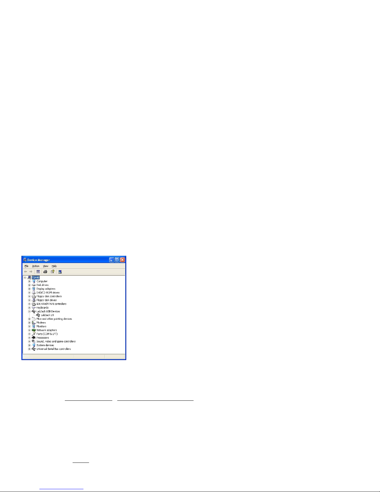
If LJControlPanel does not find the U3, check Windows Device Manager to see if the U3 installed correctly. One wa y to get to the
Device Manager is:
Start => Control Panel => System => Hardware => Device Manager
The entry for the U3 should appear as in the following figure. If it has a yellow caution symbol or exclamation point symbol, rightclick and select “Uninstall” or “Remove”. Then disconnect and reconnect the U3 and repeat the Found New Hardware Wizard as
described above.
Correctly Functioning U3 in Windows Device Manager
Linux and Mac OS X
The Exodriver is the native USB driver for Linux and Mac OS X. With it you can use low-level functions to interact with your U3 over
USB. The LJUD driver, LJControlPanel and LJSelfUpgrade applications are not available for Linux or Mac OS X.
Download the Exodriver at labjack.com/support/software or lab jack.com/support/linux-and-mac-os-x-drivers. For Mac OS X you
can use the Mac Installer for installation, otherwise use the source code and install script.
Mac OS X Installer
Unzi p the contents of Exodrive r_NativeUSB_Setup.zip and run E xodriver_NativeUSB_Setup.pkg. Then follow the installer’s
instructions to install the driver.
Source Code
Mac OS X Requirements
• OS X 10.5 or newer
• XCode developer tools
• libusb-1.0 library available at li busb.info
Linux Requirements
2
Page 3
• Linux kernel 2.6.28 or newer.
• GNU C Compiler
• libusb-1.0 library and development files (header files)
Installation
To install the driver from source code, first unzip the contents of the Exodriver source code. Then run the following commands in a
terminal (replace <Exodriver-Source-Directory> with the directory yo u unzipped the Exodriver source code to):
cd <Exodriver-Source-Directory>
sudo ./install.sh
Follow the install script’s instructions to install the driver.
For more Exodriver installa tion information go to the Exodriver page at labjack.com/sup port/linux-and-mac-os-x-drivers. The
source code download’s README, INSTALL.Li nux and INS TALL.MacOSX also provides more information. If you run into
problems, first take a look at the comments section of the Exodriver page as the issue may have been helped wi th previously.
After installation, to test your U3 connect it to your computer with a USB cable. The USB cable provides data and power. Build and
run one of the examples from the source code download. Alternatively, install LabJackPython (at
labjack.com/sup port/labjackpython) and run one of i ts examples.
1.1 - Control Panel Application (LJControlPanel)
The application LJControlPanel is included with the installation package below
LabJack Windows Driver and Software Installation Package
Name: LabJack-2014-10-14.exe
Size: 49.99 MB
Upload date: 2014-10-14 12:45
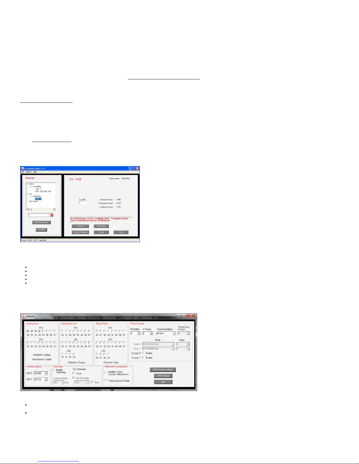
The LabJack Control Panel application (LJCP) handles configuration and testing of the UD series hardware. Click on the “Find
Devices” button to search for connected devices.
Figure 1-1. LJControlP anel Main Window
Figure 1-1 shows the results from a typical search. The application found two devices. The USB connection for a U3 has been
selected in Figure 1-1, bringing up the configuration window on the right side.
Refresh: Reload the window using values read from the device.
Write Values: Write the Local ID from the wi ndow to the device.
Config Defaults: Opens the window shown in F igure 1-2.
Reset: Click to re set the selected device.
Test: Opens the window shown in Figure 1-3.
Config Defaults:
This option provides control over the condition of the device at power-up or reset. Figure 1-2 shows a U3-HV with the fa ctory
default power-up configuration, whi ch means AIN0-AIN3 set to analog inp ut, F IO4 to CIO3 set to digital input, analog outputs set to
minimum voltage (near 0), a nd timers/counters/watchdog disabled.
Figure 1-2. LJControlP anel U3 Configure Defaults Window
Write Factory Values: Clicking this wi ll set everything back to the factory defaults and write those factory defaults to
nonvolatile memory.
Write Values: Change any desi red settings, a nd then click this to write the new settings to nonvolatile memory.
Test Panel:
Figure 1-3 shows the test window for a U3 device. This window co ntinuously (once per second) writes to and reads from the
selected LabJack.
3
Page 4
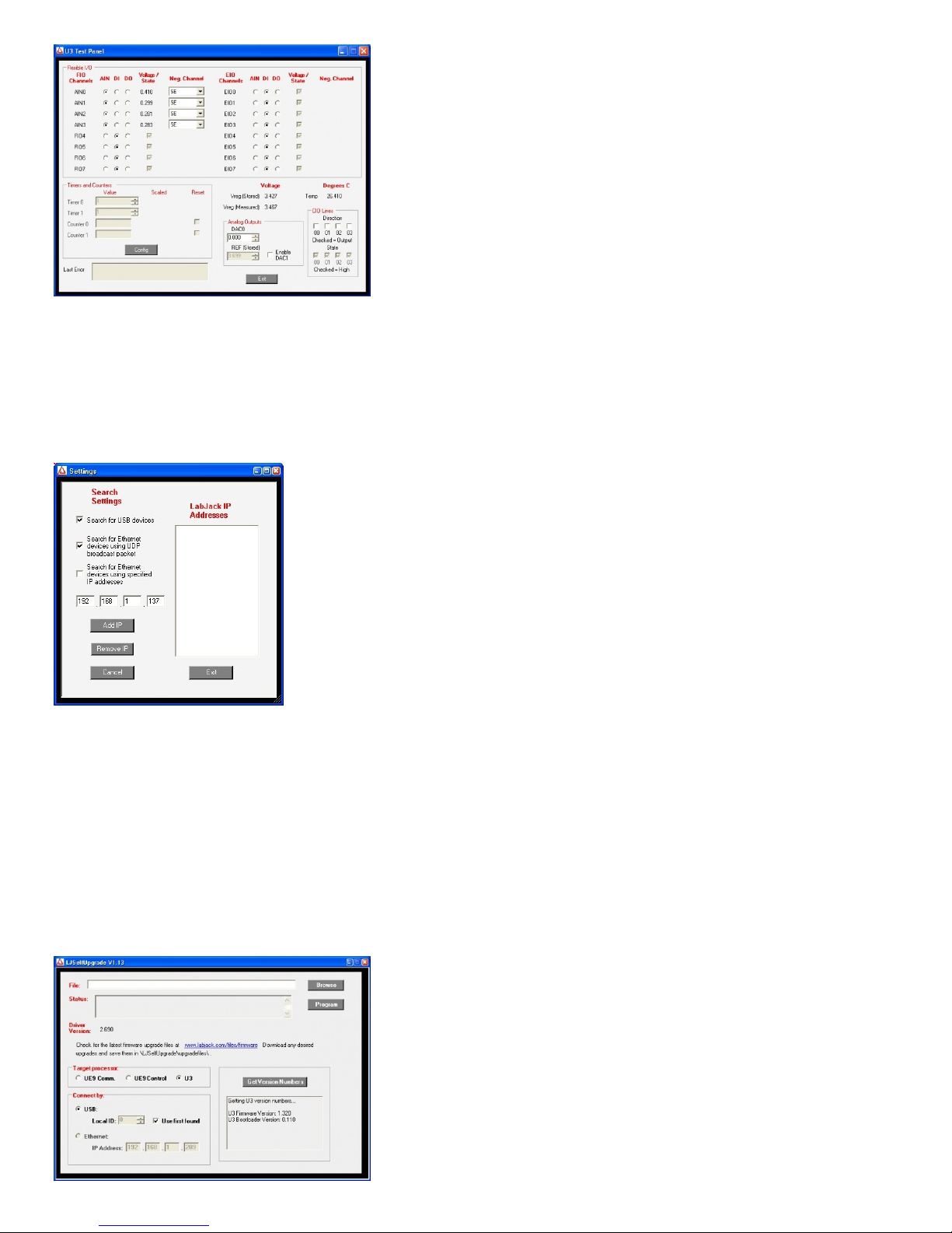
Figure 1-3. LJControlP anel U3 Test Window
Any configuration done on this screen is not written to no nvolatile memory. These settings just affect the current condition of the
device, not the reset/power-up condition.
When the test panel first loads it sets everything to factory default, so previous settings (or reset/power-up settings) will not be
shown.
LJCP Settings:
Selecting Options=>Settings from the main LJControlPanel menu brings up the window shown in Figure 1-4. Thi s window allows
some features to of the LJControlP anel application to be customized.
Figure 1-4. LJControlP anel Setting s Window
Search for US B devices: If selected, LJControlPanel will include USB when searching for devices.
Search for Ethernet devices using UDP broadcast packet: Only a pplies to UE9 device.
Search for Ethernet devices using specified IP addresses: Only applies to UE9 device.
LJControlPanel is normally installed by the main LabJack installer, which is the link at the top of the page.
1.2 - Self-Upgrade Application (LJSelfUpgrade)
The processor in the U3 has field upgradeable flash memory. The self-upgrade application shown in Figure 1-5 programs the
latest firmware onto the processor.
USB is the only interface on the U3, and first fo und is the only option for self-upgrading the U3, so no chang es are needed in the
“Connect by:” box. There must only be one U3 connected to the PC when running LJSelfUpgrade.
Click on “Get Version Numbers”, to find out the current firmware versions on the device. Then use the provided Internet link to go to
labjack.com and check for more recent firmware. D ownload firmware files to the …\LabJack\LJSelfUpgrade\upgradefiles\
directory.
Click the Browse button and select the upgrade file to program. Click the Program button to begin the self-upgrade process.
4
Page 5
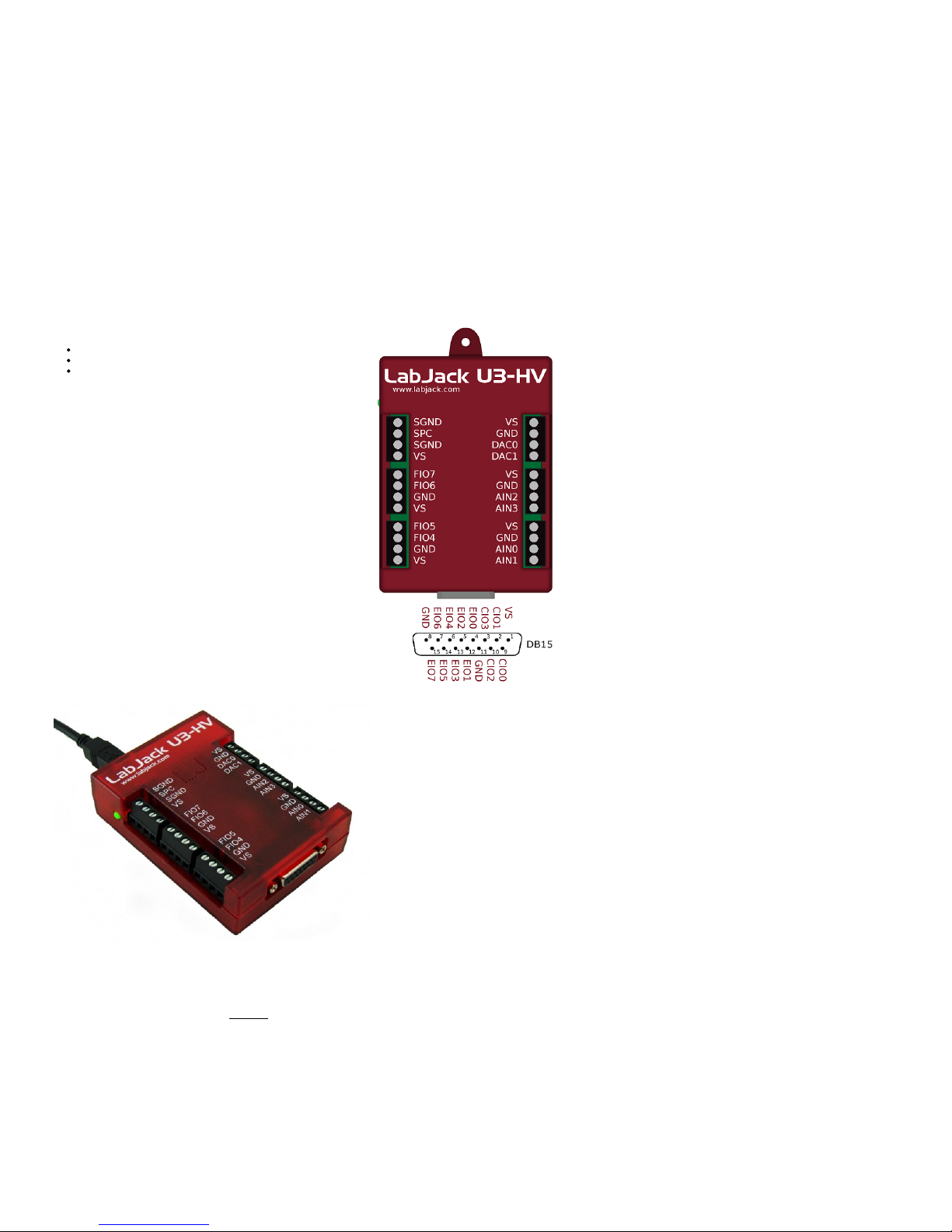
Figure 1-5. Self-Upgrade Application
If problems are encountered during programming, try the following:
1. Unplug the U3, wait 5 seconds then reconnect the U3. Click OK then press program again.
2. If step 1 does not fix the problem unplug the U3 and watch the LED while plugging the U3 back in. Follow the following steps
based on the LED's activity.
1. If the LED is blinking continuously (flash mode), connect a jumper between F IO4 and SPC (FIO0 to SCL on U3
1.20/1.21), then unplug the U3, wait 5 seconds and plug the U3 back in. Try programming again (disconnect the jumper
before programming).
2. If the LED blinks several times and stays on, connect a jumper between F IO5 and SPC (FIO1 to SCL on U3
1.20/1.21), then unplug the U3, wait 5 seconds and plug the U3 back in. Try programming again (disconnect the jumper
before programming).
3. If the LED blinks several times and stays off, the U3 is no t enumerating. Please restart your computer and try to
program again.
4. If there is no LED activity, connect a jumper between FIO5 and SPC (FIO1 to SCL on U3 1.20/1.21), then unplug the
U3, wait 5 seconds and plug the U3 back in. If the LED is blinking continuously click OK and program again (after
removing the jumper). If the LED does not blink connect a jumper between F IO4 and SPC (FIO0 to SCL on U3
1.20/1.21), then unplug the U3, wait 5 seconds and plug the U3 back in.
5. If the LED does a repeating pattern of 3 blinks then pause, the U3 has detected internal memory corruption and
you will have to contact LabJack Support.
3. If there is no activity fro m the U3's LED after following the above steps, please contact support.
2 - Hardware Description
The U3 has 3 different I/O areas:
Communication Edge,
Screw Terminal Edge,
DB Edge.
The communication edge has a USB type B connector (with black cable
connected in Fi gure 2-1). All power a nd communication is handled by the
USB interface.
The screw terminal edge has convenient connections for the analog outputs
and 8 flexible I/O (digital I/O, analog inputs, timers, or counters). The screw
terminals are arranged in blocks of 4, with each block consisting of Vs, GND,
and two I/O. There is also a status L ED located on the left edge.
The DB Edge has a D-sub type conne ctors called DB15 which has the 8 EIO
lines and 4 CIO lines. The EIO lines are flexible like the FIO lines, while the
CIO are d edicated digital I/O.
Figure 2-1. LabJack U3
2.1 - USB
For information ab out US B installation, see Section 1.
The U3 has a full-speed USB connection compatible with USB version 1.1 or 2.0. Thi s connection provides communication and
power (Vusb). USB ground is connected to the U3 ground (GND), and USB ground is generally the same as the ground of the PC
chassis and A C mains.
The details of the U3 USB interface are handled by the high level d rivers (Windows LabJackUD DLL), so the following information
is really only needed when developing low-level drivers.
The LabJack vendor ID is 0x0CD5. The product ID for the U3 is 0x0003.
The USB interface consists of the normal bidirectional control endpoint (0 OUT & IN), 3 used bulk endpoints (1 OUT, 2 IN, 3 IN),
and 1 dummy endpoint (3 OUT). Endpoint 1 consists of a 64 byte OUT endpoint (address = 0x01). Endpoint 2 consists of a 64
byte IN endpoint (address = 0x82). Endpoint 3 consists of a dummy OUT endpoint (address = 0x03) and a 64 byte IN endpoint
(address = 0x83). Endpoint 3 OUT i s not supported by the firmware, and should never be used.
All commands should always be sent on Endpoint 1, and the responses to commands will always be on Endpoint 2. Endpoint 3 is
5
Page 6

only used to send stream data from the U3 to the host.
2.2 - Status LED
There is a green status LED on the LabJack U3. This LED blinks on reset, and then remains steadily li t. Other LED behavior is
generally related to flash upgrade modes ("Section 1.2":/support/u3/users-guide/1.2).
Normal Power-Up Status LED Behavior: When the USB cable is connected to the U3, the Status LED blinks 5-6 ti mes over 2
seconds and then remains solid on.
LED blinking continuously at about 4 Hz, even with no software running: This indicates that the U3 is in flash mode. See
Section 1.2 and reprogram the device.
2.3 - GND and SGND
The GND conne ctions available at the screw-terminals and DB connectors provide a common ground for all LabJack functio ns. All
GND terminals are the same and connect to the same ground plane. This ground is the same as the ground line on the USB
connection, whi ch is often the same as ground on the PC chassis and therefore AC mains ground.
SGND is located near the upper-left of the device. This terminal has a self-resetti ng thermal fuse in series with GND . Thi s is often
a good terminal to use when connecting the ground from another separately powered system that could unknowingly already share
a common ground with the U3.
See the AIN, DAC, and Digital I/O Sections for more information about grounding.
2.4 - VS
The Vs terminals are designed as outputs for the internal supply voltage (nominally 5 volts). This will be the volta ge provided from
the USB cable. The Vs connections are outputs, not inputs. Do not connect a power source to Vs in normal situations. All Vs
terminals are the same.
2.5 - Flexible I/O (FIO/EIO)
The FIO and EIO ports on the LabJack U3 can be individually configured as digital input, digital output, or analog input. Thi s is
FIO0-EIO7 on the U3-LV (16 lines), or FIO4-EIO7 on the U3-HV (12 lines). In addi tion, up to 2 of these li nes can be configured as
timers, and up to 2 of these lines can be configured as counters. If a line is configured as analog, it is called AINx according to the
following table:
AIN0
FIO0
AIN8
EIO0
AIN1
FIO1
AIN9
EIO1
AIN2
FIO2
AIN10
EIO2
AIN3
FIO3
AIN11
EIO3
AIN4
FIO4
AIN12
EIO4
AIN5
FIO5
AIN13
EIO5
AIN6
FIO6
AIN14
EIO6
AIN7
FIO7
AIN15
EIO7
Table 2. 5-1. Analog Input Pin Locatio ns
On the U3-HV, compared to the -LV, the first four flexible I/O are fixed as analog inputs (AIN0-AIN3) with a nominal ±10 volt input
range. All di gital operations, including analog/digital confi guration, a re ignored on these 4 fixed analog inputs.
Timers and counters can appear on vario us pins, but other I/O lines never move. For example, Timer1 can appear anywhere from
FIO4 to EIO1 , depending on TimerCounterPinOffset and whether Timer0 is enabled. On the other hand, FIO5 (for example), i s
always on the screw terminal labeled FIO5, and AIN5 (if enabled) is always on that same screw termina l.
The first 8 flexible I/O lines (FIO0-FIO7) appear on built-in screw terminals. The other 8 flexible I/O lines (EIO0-EIO7) are available
on the DB 15 connector.
Many software applications will need to initialize the flexible I/O to a known pin configuration. That requires calls to the low-level
functions ConfigIO and ConfigTi merClock. Following are the values to set the pin configuration to the factory default state:
Byte #
6
WriteMask
15
Write all parameters
8
TimerCounterConfig
0
No Timers/Counters. Offset = 4
9
DAC1 Enable
0
DAC1 Disabled. (Ignored on HW 1.3)
10
FIOAnalog
0
FIO all digital.
11
EIOAnalog
0
EIO all digital.
Table 2. 5-2. ConfigIO Fa ctory Defaul t Value s
Byte #
8
TimerClockConfig
130
Set cloc k to 48MHz.
9
TimerClockDivisor
0
Divisor = 0.
Table 2. 5-3. ConfigTime rClock Factory Default Va lues
When using the high-level LabJackUD driver, thi s could be done with the following requests:
ePut (l ngHandle , LJ_io PUT_CONF IG, LJ_c hNUMBER _TIMERS_ ENABLED, 0, 0);
ePut (l ngHandle , LJ_io PUT_CONF IG, LJ_c hTIMER_ COUNTER_ PIN_OFFS ET, 4, 0);
ePut (l ngHandle , LJ_io PUT_CONF IG, LJ_c hTIMER_ CLOCK_BA SE, LJ_t c48MHZ, 0);
ePut (l ngHandle , LJ_io PUT_CONF IG, LJ_c hTIMER_ CLOCK_DI VISOR, 0 , 0);
ePut (l ngHandle , LJ_io PUT_COUN TER_ENAB LE, 0, 0, 0);
ePut (l ngHandle , LJ_io PUT_COUN TER_ENAB LE, 1, 0, 0);
ePut (l ngHandle , LJ_io PUT_DAC_ ENABLE, 1, 0, 0 ); //Ig nored on hardwa re rev 1 .30+.
ePut (l ngHandle , LJ_io PUT_ANAL OG_ENABL E_PORT, 0, 0, 1 6);
… or with a single request to the following IOType created exactly for this purpose:
ePut (l ngHandle , LJ_io PIN_CONF IGURATIO N_RESET , 0, 0, 0);
2.6 - AIN
The LabJack U3 has up to 16 analog inputs available on the flexi ble I/O lines (FIO0-FIO7 and EIO0-EIO7). Single-ended
measurements can be taken of any line compared to ground, or differential measurements can be taken of any line to any other
line.
Analog input resolutio n is 12-bits. The range of single-ended analo g inputs is normally about 0-2.44, and there is a “special” 0-3.6
volt range available. The range of differential analog inputs is typically ± 2.4 volts, but is pseudobipolar, not true bipolar. The
difference (positive channel minus negative channel) can be -2.4 volts, but neither input can have a voltage less than -0.3 volts to
6
Page 7

ground. For valid measurements, the voltage on every low-voltage analog input pin, with respect to ground, must be within -0.3 to
+3.6 volts. See Appendix A for voltage limits to avoid damage.
On the U3-HV, compared to the -LV, the first four flexible I/O are fixed as analog inputs (AIN0-AIN3), and have scaling such that the
input range is a true bipolar ±10 volts normally, and -10 to +20 volts when using the “special” range . The input impedance of these
four lines is roughly 1 MΩ, which is good, but less than the normal low voltage analog inputs. Analog/digital configuration and all
other digital operations on these pins are ignored. FIO4-EIO7 a re still available as flexible I/O, same as the U3-LV.
To get the special 0-3.6 volt or -10/+20 volt range, you do a differential reading with the negative channel set to 32, altho ugh the
reading is actually single-ended.
Because the scaling on the high-voltage inputs on the U3-HV (AIN0-AIN3) is inherently single-ended, a factory calibration is not
possible for differential readings. If a differential reading is requested where either channel is a high-voltage channel, the driver will
return the raw binary reading and the user must handle calibration/conversion.
The analog inputs have a Qui ckSample option where each conversion is done faster at the expense of increased noise. This is
enabled by passing a nonzero value for put_config special channel LJ_chAIN_RE SOLUTION. There is also a LongSettling option
where additional settling time is added between the internal multiplexer configuration and the analog to digital conversion. This
allows signals with more source impedance, and is enabled by passing a nonzero value for put_config special channel
LJ_chAIN_SE TTLING_TIME . Both o f these options are disabled by de fault. This applies to command/response mode only, and
the resulting typical data rates are discussed in Section 3.1. For stream mode, see Section 3.2.
Note that sinking excessive current i nto digital outputs can cause substanti al errors in analog input readings. S ee Section 2.8.1.4
for more info.
2.6.1 - Channel Numbers
The LabJack U3 has up to 16 external analog inputs, plus a few internal channels. The low-level functions specify a positive and
negative channel for each analog input conversion. With the LabJackUD driver, the IOType LJ_ioGET_AIN i s used for singleended channels only, and thus the negative channel is internally set to 31. There is an additional IOType called
LJ_ioGET_AIN_DIFF that allows the user to specify the positive and negative channel.
Positive Channel #
0-7
AIN0-AIN7 (FIO0-FIO7)
8-15
AIN8-AIN15 (EIO0-EIO7)
30
Temp Sensor
31
Vreg
Table 2. 6.1-1. Positive Cha nnel Numbe rs
Negative Channel #
0-7
AIN0-AIN7 (FIO0-FIO7)
8-15
AIN8-AIN15 (EIO0-EIO7)
30
Vref
31 or 199
Single-Ended
32
Special 0-3.6 or -10/+20 (UD Only)
Table 2. 6.1-2 Negati ve Channe l Numbers
Positive channel 31 puts the internal Vreg (~3.3 volts) on the posi tive input of the ADC . See Section 2.6.4 for information about the
internal temperature sensor.
If the negative channel is set to anything besides 31/199, the U3 does a differential conversion and returns a pseudobipolar value.
If the negative channel is set to 31/199, the U3 does a single-ended conversion and returns a unipolar value. Channel 30 puts the
internal voltage reference Vref (~2.44 volts) on the negative input of the ADC.
Channel 32 is a special negative channel supported by the LabJack UD driver. When used, the driver will actually pass 30 as the
negative channel to the U3, and when the result is returned the d river adds Vref to the value. For a low-voltage analog input this
results in a full span on the positive channel of about 0 to 4.88 volts (versus ground), but since the voltage on any analog input
cannot exceed 3.6 volts, only 75% of the converter’s range is used and the span is about 0 to 3.6 volts. For a high-voltage analog
input, channel 32 (special range) results in a span of about -10 to +20 volts.
In the U3 examples that accompany the Exodriver, u3.c also supports channel 32 in calls to eAIN().
Channel 32 is also supported in LabJackPython:
# On th e U3, wi re a ju mper fro m DAC0 t o FIO0, then ru n:
>>> imp ort u3
>>> d = u3.U3()
>>> d.c onfigIO( FIOAnal og = 1) # Set FI O0 to a nalog
>>> d.w riteRegi ster(50 00, 3) # Set DAC 0 to 3 V
>>> d.g etAIN(0, 32)
3.01411 40941996 127
For the four high-voltage channels on the U3-HV, the special channel negative channel also puts Vref on the negative. This results
in an overall range of about -10 to +20 volts on the positive input.
2.6.2 - Converting Binary Readings to Voltages
This information is only needed when using low-level functions and other ways of getting binary readings. Readings in volts already
have the calibration constants applied. The UD driver, for example, normally returns voltage readings unless binary readings are
specifically requested.
Following are the nomi nal input voltage ranges for the low-voltage analog inputs. This is all analog inp uts on the U3-LV, and AIN4AIN15 on the U3-HV.
Max V
Min V
Single-Ended
2.440Differential
2.44
-2.44
Special 0-3.6
3.60Table 2. 6.2-1. Nomina l Analog In put Voltage Range s for Low-Voltage Channe ls
Max V
Min V
Single-Ended
10.3
-10.3
Differential
N/A
N/A
Special -10/+20
20.1
-10.3
Table 2. 6.2-2. Nomina l Analog In put Voltage Range s for High-Voltage Chan nels
Note that the minimum differential input voltage of -2.44 volts means that the posi tive channel can be as much as 2.44 volts less
than the negative channel, not that a channel can measure 2.44 volts less than ground. The voltage of any lo w-voltage analog input
pin, compared to ground, must be in the range -0.3 to +3.6 volts.
The “special” range (0-3.6 on lo w-voltage channels and -10/+20 volts on high-voltage channels) is obtained by doing a differential
measurement where the negative channel is set to the internal Vref (2.44 volts). For low-voltage channels, simply do the low-
7
Page 8

voltage differential conversion as described below, then add the stored Vref value. For hi gh-voltage channels, d o the same thing,
then multip ly by the proper high-voltage slope, divide by the single-ended low-voltage slope, and add the proper high-voltage
offset. The UD driver handles these conversions auto matically.
Althoug h the binary readings have 12-bit resolution, they are returned justified as 16-bit value s, so the approximate nominal
conversion from binary to voltage is:
Volts(u ncalibra ted) = (Bits/65 536)*Spa n (Sing le-Ended )
Volts(u ncalibra ted) = (Bits/65 536)*Spa n – Spa n/2 (Dif ferentia l)
Binary readings are always unsigned integers.
Where span i s the maximum voltage minus the minimum vo ltage from the tables above. The actual nominal conversions are
provided in the tables below, and should be used if the actual calibration constants are not read for some reason. Most
applications will use the actual calibrations consta nts (S lope and Offset) stored in the internal flash.
Volts = (Slope * Bits) + Offse t
Since the U3 uses multiplexed channels connected to a single ana log-to-digital converter (ADC), all low-voltage channels have the
same calibration for a given configuration. High-voltage channels have individual sca ling circuitry out front, and thus the calibration
is unique for each channel.
See Section 5.4 for detail about the location of the U3 calibration constants.
2.6.2.1 - Analog Inputs With DAC1 Enabled (Hardware
Revisions 1.20 & 1.21 only)
This Section only applies to the older hardware revi sions 1.20 and 1.21. Starting wi th hardware revision 1.30, DAC1 is always
enabled and does not affe ct the analog inputs.
The previous information assumed that DAC1 is disabled. If DAC1 is enabled, then the internal reference (Vref = 2.44 volts) is not
available for the ADC, and instead the internal regulator voltage (Vre g = 3.3 volts) is used as the reference for the AD C. Vreg is
not as sta ble as Vref, but more stable than Vs (5 volt power supply). Following are the nominal input voltage ranges for the analog
inputs, assuming that DAC1 is enabled.
Max V
Min V
Single-Ended
3.30Differential
3.3
-3.3
Special -10/+20
N/A
N/A
Table 2. 6.2.1-1. Nomina l Analog I nput Voltage Ranges (DAC1 Enable d)
Note that the minimum differential input voltage of -3.3 volts means that the positive channel can be as much as 3.3 volts less than
the nega tive channel, not that a channel can measure 3.3 vo lts less than ground. The voltage of any analog input pi n, compared to
ground, must be in the range -0.3 to +3.6 volts, for specified performance. See Appendix A for voltage limits to avoid damage.
Negative channel numbers 30 and 32 are not valid with DA C1 enabled.
When DAC1 is enabled, the slope/offset calibration co nstants are not used to convert raw readings to voltages. Rather, the Vreg
value is retrieved from the Mem area, and used with the approximate single-ended or differential conversion equations above,
where Span i s Vreg (single-ended) or 2Vreg (differential).
2.6.3 - Typical Analog Input Connections
A common question is “can this sensor/signal be measured with the U3”. Unless the signal has a voltage (referred to U3 ground)
beyond the limits in Appendix A , it can be connected without damaging the U3, b ut more thought is required to determine what is
necessary to make useful measurements with the U3 or any measurement devi ce.
Voltage (versus ground): The single-ended analog inputs on the U3 measure a voltage with respect to U3 ground. The differential
inputs measure the voltage difference between two channels, but the voltage on each cha nnel with respect to ground must sti ll be
within the common mode limits specified in Appendix A. When measuring parameters other than voltage, or volta ges too big or
too small for the U3, some sort of sensor or transducer is required to produce the proper voltage signal. Examples are a
temperature sensor, amplifier, resistive voltage divider, or perhaps a combination of such things.
Impedance: When connecting the U3, or any measuring device, to a signal source, it must be considered what impact the
measuring devi ce will have on the signal. The main consideration is whether the currents going into or out of the U3 analog input
will cause noticeable voltage errors due to the impedance of the source. To maintain consistent 1 2-bit results, it is recommended
to keep the source impedance within the limits specified in App endix A.
Resolution (and Accuracy): Based on the measurement type and resolution of the U3, the resolution can be determined in terms of
voltage or engineering units. For example, assume some temperature sensor provi des a 0-10 mV signal, corresponding to 0-100
degrees C. Samples are then acquired with the U3 using the 0-2.44 volt single-ended input range, resulting in a voltage resolution
of about 2.44/4096 = 596 µV. That means there wi ll be about 17 discrete steps across the 10 mV span of the signal, and the
temperature resolution is about 6 degrees C. If this experiment re quired a resolution of 1 degrees C, this configuration would not
be sufficient. Accuracy will also need to be considered. Appendix A places some boundaries on expected accuracy, but an insystem calibration can generally be done to provide absolute accuracy down to the linearity (INL) li mits of the U3.
Speed: How fast does the signal need to be sampled? For instance, if the sig nal is a waveform, what information is needed: peak,
average, RMS, shape, frequency, … ? Answers to these questions will help decid e how many points are needed per waveform
cycle, a nd thus what sampling rate is required. In the case of multiple channels, the scan rate is also consi dered. See Sections 3.1
and 3.2.
2.6.3.1 - Signal from the LabJack
One example of measuring a signal from the U3 i tself, is wi th an analog output. All I/O on the U3 share a common ground, so the
voltage on an analog output (DAC) can be measured by simply connecting a single wire from that terminal to an AIN te rminal
(FIO/E IO). The analog output must be set to a voltage within the range of the analog input.
2.6.3.2 - Unpowered Isolated Signal
An example of an unpowered isolated signal would be a photocell where the sensor leads are not shorted to any external voltages.
Such a sensor typi cally has two leads, where the posi tive lead connects to an AIN terminal and the negative lead connects to a
GND terminal.
2.6.3.3 - Signal Powered By the LabJack
A typi cal example of thi s type of signal is a 3-wi re temperature sensor. The sensor has a power and ground wire that connect to Vs
and GND on the LabJack, and then has a signal wire tha t simply connects to an AIN terminal.
8
Page 9
Another variation is a 4-wire sensor where there are two signal wires (positive and nega tive) rather than one. If the negative signal
is the same as power ground, or can be shorte d ground, the n the positive signal can be connected to AIN a nd a single-ended
measurement can be made. A typical example where this does not work is a bridge type sensor, such as pressure sensor,
providing the raw bridge output (and no amplifier). In this case the signal voltage is the difference between the positive and
negative signal, and the negative signal ca nnot be shorted to ground. Such a signal could be measured using a differenti al input
on the U3.
2.6.3.4 - Signal Powered Externally
An example is a box wi th a wire coming out that is defined as a 0-2 volt analog signal and a second wire labeled as ground. The
signal is known to have 0-2 volts compared to the ground wire, but the complication is what is the voltage of the box ground
compared to the LabJack ground.
If the box is known to be electrically isolated from the LabJack, the box ground can simply be connected to LabJack GND . An
example would be if the box was plastic, powered by an internal battery, and does not have any wires besides the signal and
ground which a re connected to AINx and GND on the LabJack.
If the box ground is known to be the same as the LabJack GND, then perhaps only the one signal wire needs to be connected to
the LabJack, but it generally does not hurt to go ahead and connect the ground wire to LabJack GND with a 100 Ω resistor. You
definitely do not want to connect the grounds without a resistor.
If little is known about the box ground, a DMM can be used to measure the voltage of box ground compared to LabJack GND. As
long as an extreme voltage is not measured, it is generally OK to connect the box ground to LabJack GND, b ut it is a good idea to
put in a 100 Ω series resistor to prevent large currents from flowing on the ground. Use a small wattage resistor (typi cally 1/8 or 1/4
watt) so that i t blows if too much current does flow. The only current that should flow on the ground is the return of the analog inp ut
bias current, whi ch is only microamps.
The SGND terminals (on the same terminal block as SPC) can be used instead of GND fo r externally powered signals. A series
resistor is not needed as SGND is fused to prevent overcurrent, but a resistor will eliminate confusion that can be caused if the
fuse is tri pping and resetting .
In general, if there is uncertainty, a good approach is to use a DMM to measure the voltage on each sig nal/ground wi re without any
connections to the U3. If no large voltages are noted, connect the ground to U3 SGND with a 100 Ω series resistor. Then again use
the DMM to measure the voltage of each signal wi re before connecting to the U3 .
Another g ood general rule is to use the minimum number of ground connections. For instance, if connecting 8 sensors powered by
the same external supply, or otherwise referred to the same external ground, only a single ground connection is needed to the U3.
Perhaps the ground leads from the 8 sensors would be twisted together, and then a single wire would be connected to a 100 Ω
resistor which is conne cted to U3 ground.
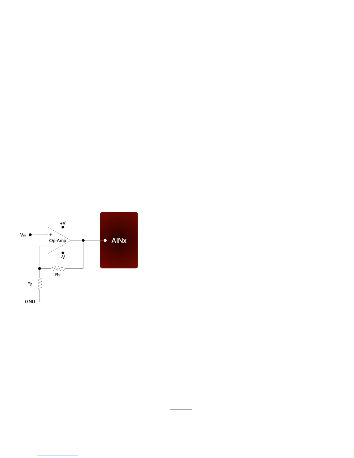
2.6.3.5 - Amplifying Small Signal Voltages
The best results are generally obtained when a signal voltage spans the full analog input range of the LabJack. If the signal is too
small it can be amplified before connecting to the LabJack. One good way to handle low-level signals such as thermocouples is
the LJTick-InA mp, whi ch is a 2-cha nnel instrumentation amplifier module that plugs into the U3 screw-terminals.
For a do-it-yourself solution, the following figure shows an operational amplifier (op-amp) configured as non-inve rting:
Figure 2.6-1. Non-Inverting Op-Amp Configuration
The gain of thi s configuration is:
Vout = Vin * (1 + (R2/ R1))
100 kΩ is a typical value for R2. Note that if R2=0 (short-circuit) and R1=inf (not installed), a simple buffer with a gain equal to 1 is
the result.
There are numerous criteria used to choose an op-amp fro m the thousands that are avai lable. One of the main criteria is that the
op-amp can handle the input and output signal range. Often, a single-supply rail-to-rail input and output (RIRO) is used as it can be
powered from Vs and GND and pass signals withi n the range 0-Vs. The OPA344 from Texas Instruments (ti.com) is good for many
5 volt applications.
The op-amp is used to amplify (and buffer) a signal that is referred to the same ground as the LabJack (single-ended). If instead
the signal is differential (i.e. there is a positive and negative signal both of which are different than ground), an i nstrumentation
amplifier (in-amp) should be used. An in-amp converts a differential signal to single-ended, and generally has a simple method to
set gain.
2.6.3.6 - Signal Voltages Beyond 0-2.44 Volts (and
Resistance Measurement)
The normal input range for a low voltage analog input channel (FIO/E IO) on the U3 is about 0-2.44 volts. There is also a Special 0-
3.6V range available on those inputs. The easiest way to handle la rger voltages is often by usi ng the LJTick-Di vider, which is a two
channel buffered divider module tha t plugs into the U3 screw-terminals.
The basic way to handle higher unipolar voltages is with a resistive voltage divider. The following figure shows the resistive voltage
divider assuming that the source voltage (Vin) is referred to the same ground as the U3 (GND).
9
Page 10
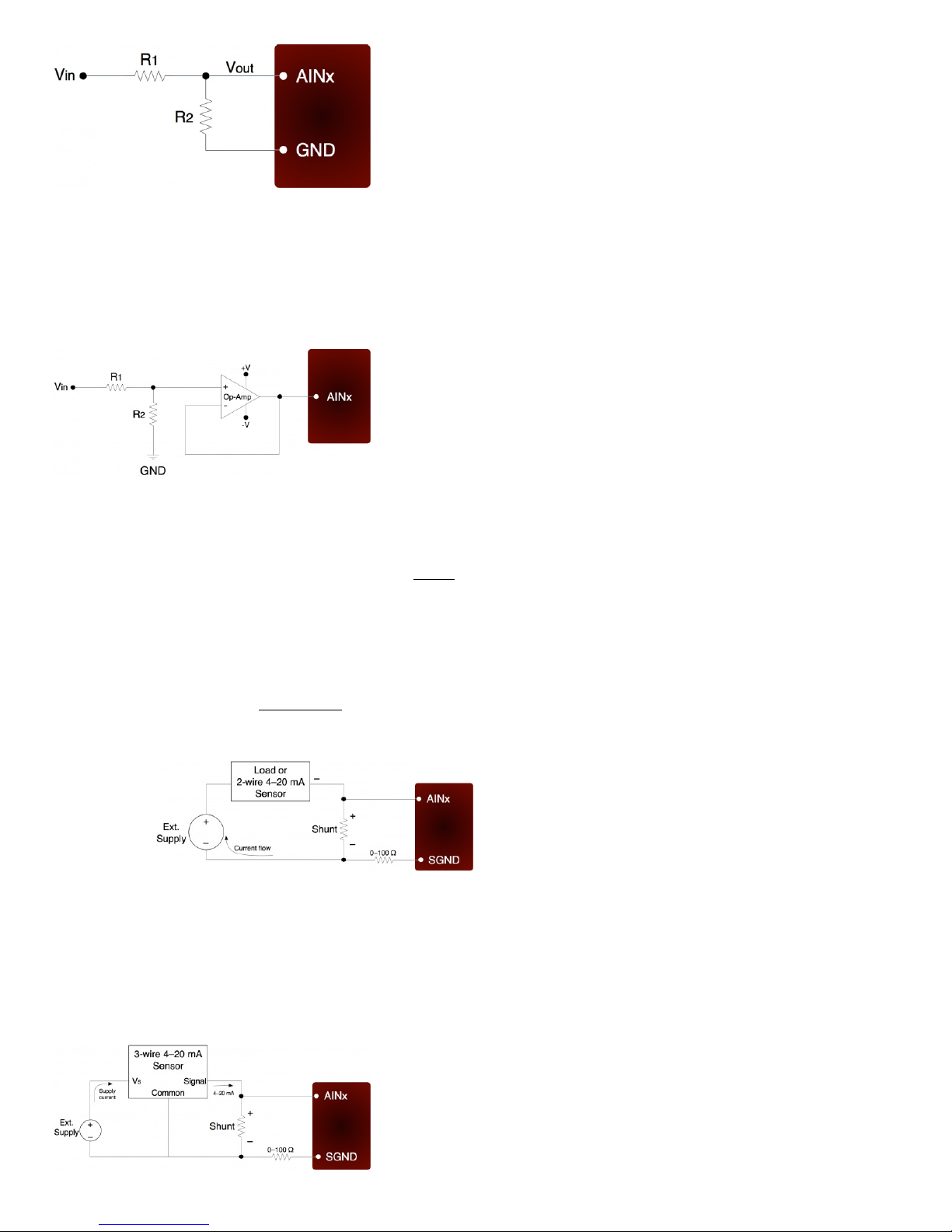
Figure 2.6-2. Vo ltage Divider Circuit
The attenuation of this circuit i s determined by the equation:
Vout = Vin * ( R2 / (R 1+R2))
This divider is easily implemented by putting a resistor (R1) in series with the signal wire, and placing a second resistor (R2) from
the AIN terminal to a GND terminal. To maintain specified analog input performance, R1 should not excee d the values specified in
Appendix A, so R1 can generally be fixed at the max recommended value and R2 can be adjusted for the desi red attenuation.
The divide by 2 configuration where R1 = R2 = 10 kΩ (max source impedance limit for lo w-voltage channels), presents a 20 kΩ
load to the source, meaning that a 5 volt signal will have to be able to source/sink up to +250 µA. Some signal sources might
require a load with hi gher resistance, in which case a buffer should be used. The following figure shows a resistive voltage divider
followed by an op-amp configured as non-inverti ng unity-gain (i.e. a buffer).
Figure 2.6-3. Buffered Voltage Divider Circuit
The op-amp is chosen to have low input bias currents so that large resistors can be used in the voltage divider. For 0-5 volt
applications, where the amp will be powered from Vs and GND, a good choice would be the OPA344 from Texas Instruments
(ti.com). The OPA344 has a very small bias current that changes li ttle across the entire voltage range. Note that when powering the
amp from Vs and GND, the input and output to the op-amp is limited to that range, so if Vs is 4.8 volts your signal range will be 0-
4.8 volts.
To handle bipolar voltages, you also need offset or level-shifting. Refer to application note SLOA097 from ti .com for more
information.
The information above also applies to resistance measurement. A common way to measure resistance is to build a voltage
divider as shown in Figure 2.6-2, where one of the resistors is known and the other is the unknown. If Vin is known and Vout is
measured, the vo ltage divider equation can be re arranged to solve for the unknown resistance.
2.6.3.7 - Measuring Current (Including 4-20 mA) with a
Resistive Shunt
The best way to handle 4-20 mA si gnals is with the LJTick-CurrentS hunt, which is a two cha nnel active current to voltage converter
module that plugs into the UE 9 screw-terminals.
The following figure shows a typical metho d to measure the current through a load, or to measure the 4-20 mA signal produced by
a 2-wire (loop-powered) current loop sensor. The current shunt shown in the figure is simply a resistor.
Figure 2.6-4. Current Measurement With Arbitrary Load or 2-Wire 4-20 mA Sensor
When measuring a 4-20 mA signal, a typi cal value for the shunt would be 120 Ω. This results in a 0.48 to 2.40 volt signal
corresponding to 4-20 mA. The external supply must provide enough voltage for the sensor and the shunt, so if the senso r requires
5 volts the supply must provide at least 7.4 volts.
For applications besides 4-20 mA, the shunt is chosen based on the maximum current and how much voltage drop can be
tolerated across the shunt. For instance, if the maximum current is 1.0 amp, and 1.0 volts of drop is the most that can be tolerated
without affecting the load, a 1.0 Ω resistor could be used. That equates to 1.0 watts, though, which would require a special high
wattage resistor. A better solution would be to use a 0.1 Ω shunt, and then use an amplifier to increase the small voltage produced
by that shunt. If the maxi mum current to measure is too high (e.g. 100 amps), it will be difficult to find a small enough resistor and a
hall-effect sensor should be considered instead of a shunt.
The following figure shows typical connections for a 3-wire 4-20 mA sensor. A typical value for the shunt would be 120 Ω which
results in 0.48 to 2.40 volts.
Figure 2.6-5. Current Measurement With 3-Wire 4-20 mA (Sourcing) Sensor
10
Page 11

The sensor shown in the above figure is a sourcing type, where the signal sources the 4-20 mA current which is then sent through
the shunt resistor and sunk into ground. A nother type of 3-wire sensor is the sinking type, where the 4-20 mA current is sourced
from the posi tive supply, sent through the shunt resistor, and then sunk into the signal wire. If sensor ground is connected to U3
ground, the sinking type of sensor presents a problem, as at least one side of the resistor has a high common mode voltage
(equal to the positive sensor supply). If the sensor is isolated, a possible solution is to connect the sensor signal or positive sensor
supply to U3 ground (instead of sensor ground). This requires a good understanding of grounding and isolation in the system. The
LJTick-CurrentS hunt is often a simple solution.
Both figures show a 0-100 Ω resistor in series with SGND, which i s discussed in general in Section 2.6.3.4. In this case, if S GND
is used (rather than GND), a direct connection (0 Ω) should be good.
The best way to handle 4-20 mA si gnals is with the LJTick-CurrentS hunt, which is a two cha nnel active current to voltage converter
module that plugs into the U3 screw-terminals.
2.6.3.8 - Floating/Unconnected Inputs
The reading from a floating (no external co nnection) analo g input channel can be tough to predict and is likely to vary wi th sample
timing and adjacent sampled channels. Keep in mi nd that a floating channel is not at 0 volts, but rather is at an undefined voltage.
In order to see 0 volts, a 0 volt signal (such as GND) should be connected to the input.
Some data acquisition devices use a resistor, from the input to ground, to bias an unconnected input to read 0. This is often just
for “cosmetic” reasons so tha t the input reads close to 0 with floating inputs, and a reason not to do that is that thi s resistor can
degrade the input impedance of the analog input.
In a situation whe re it is desired that a floating channel re ad a particular voltage, say to detect a broken wire, a resistor (pull-down
or pull-up) can be placed from the AINx screw terminal to the desi red volta ge (GND, VS, DACx, …). A 100 kΩ resistor should pull
the analog input readings to wi thin 50 mV of any desired voltage, but obviously degrades the input impedance to 100 kΩ. For the
specific case of pulling a floating channel to 0 volts, a 1 MΩ resistor to GND can typically be used to provide analog input readings
of less than 50 mV. This information is for a low-voltage analog input channel on a U3.
Note that the four high-voltage channels on the U3 -HV do sit at a predictable 1.4 volts. You can use a pull-down or pull-up resistor
with the high-voltage inputs, but because thei r input impedance is lower the resistor must be lower (~1k might be typical) and thus
the signal is going to have to drive substantial current.
2.6.3.9 - Signal Voltages Near Ground
The nominal input range of a low-voltage single-ended analog input is 0-2.44 volts. So the nominal minimum voltage is 0.0 volts,
but the variation in that minimum can be about +/-40 mV, and thus the actual minimum voltage could be 0.04 volts.
This is not an offset erro r, but just a minimum limit. Assume the minimum limit of your U3 happens to be 10 mV. If you apply a
voltage of 0.02 volts it will read 0.02 volts. If you apply a voltage of 0.01 volts it will read 0.01 volts. If you apply a voltage less than
0.01 volts, however, it will still read the minimum limi t of 0.01 volts in thi s case.
One impact of this, is that a short to GND is usually not a good test for noise and accuracy. We often use a 1.5 volt battery for
simple tests.
If performance all the way to 0.0 is needed, use a differential reading (which is pseudobipolar). Connect some other channel to
GND with a small jumper, and then take a differential re ading of your channel compared to that grounded channel.
The nominal input range of a high-voltage single-ended analog input is +/-10 volts, so readings around 0 .0 are right in the middle
of the range and not a n issue.
2.6.4 - Internal Temperature Sensor
The U3 has an internal temperature sensor. Although this sensor measures the temperature inside the U3, which is warmer than
ambient, it has been calibrated to read actual ambient te mperature, although should only be expected to be accurate to withi n a
few degrees C. For best results the temperature o f the entire U3 must stabilize relative to the ambient temperature, whi ch can take
on the order of 1 hour. Best results will be obtained in still air in an environment with slowly changing ambient temperatures.
With the UD driver, the internal temperature sensor is read by acquiring single-ended analo g input channel 30, and returns
degrees K. Use channel 30 anywhere you would use an analog input channel (e.g. wi th eAIN).
2.7 - DAC
The LabJack U3 has 2 analog outputs (DAC0 and DAC1) that are available on the screw terminals. E ach analog output can be
set to a voltage between about 0.04 and 4.95 volts with 10 bits of resolution (8 bits on older hardware revision 1.20/1.21). The
maximum output voltage is limited by the supply voltage to the U3.
Starting with hardware revision 1.30, DAC1 is always enabled and does not affect the analog inputs, but with older hardware the
second analog output is only available in certain co nfigurations. With hardware revisions <1.30, if the analog inp uts are using the
internal 2.4 volt reference (the most accurate option), then DAC1 outputs a fixed voltage of 1.5*Vref. Also with hardware revisions
<1.30, if DAC1 is enabled the analog inputs use Vreg (3.3 volts) as the AD C reference, which is not as sta ble as the internal 2.4
volt reference.
The DAC outputs are derived as a percentage of Vreg, and then amplified by 1.5, so any changes in Vreg will have a
proportionate affect on the DAC outputs. Vre g is more stable than Vs (5 volt supply voltage), as it is the output from a 3.3 volt
regulator.
The DACs are derived from PWM signals that are affected by the timer clock frequency (Section 2.9). The default timer clock
frequency of the U3 is set to 48 MHz, and this results in the minimum DAC output noise. If the frequency is lowered, the DACs will
have more noise, where the frequency of the noise is the timer clock frequency divided by 6 5536. This effect is more exaggerated
with the 10-bit DAC s on hardware revision 1.30+, compared to the 8-bit DACs on previous hardware revisions. The noise with a
timer clock of 48/12/4/1 MHz is roughly 5/20/100/600 mV. If lower noise performance is needed at lo wer timer clock frequencies,
use the power-up default setting in LJControlPanel to force the device to use 8-bit DAC mode (uses the low-level
CompatibilityOptions byte documented in Section 5.2.2). A large capacitor (at least 220 uF) from DAC n to GND can also be used
to reduce noi se.
The analog outputs have filters with a 3 dB cutoff around 16 Hz, limiting the frequency of output waveforms to less than that.
The analog output commands are sent as raw binary values (low level functions). For a desired output voltage, the binary value can
be approximated as:
Bits(un calibrat ed) = ( Volts/4. 95)*256
For a proper calculation, though, use the calibration values (Slope and Offset) stored in the internal flash on the processor (Section
5.4):
Bits = (Slope * Volts) + Offse t
The previous apply when usi ng the original 8-bit DAC commands suppo rted on all hardware versions. To take advantage of the
10-bit resolution on hardware revision 1.30, new commands have been added (Section 5.2.5) where the binary values are aligned
to 16-bits. The cal constants are still alig ned to 8-bits, however, so the slope and offset sho uld each be multiplied by 256 before
11
Page 12
using in the above formula.
The analog outputs can withstand a continuous short-circuit to ground, even when set at maximum output.
Voltage sho uld never be applied to the analog outputs, as they are voltage sources themselves. In the event that a voltage is
accidentally applied to either analog output, they do have protection against transi ent events such as ESD (electrostatic
discharge) and continuous overvoltage (or undervoltage) of a few volts.
There is an accessory available from LabJack called the LJTick-DAC that provid es a pair of 14-bit analog outputs with a rang e of
±10 volts. The LJTick-DAC plugs into any digital I/O block, and thus up to 10 of these can be used per U3 to add 20 ana log
outputs. The LJTick-DAC has various improvements compared to the built-in DACs on the U3:
Range of +10.0 to -10.0 volts.
Resolution of 14-bits.
Slew rate of 0.1 V/μs.
Based on a reference , rather than regulator, so more accurate and stable.
Does not affect analog inputs in any configura tion.
2.7.1 - Typical Analog Output Connections
2.7.1.1 - High Current Output
The DACs on the U3 can output quite a bit of current, but they have 50 Ω of source impedance that will cause voltage drop. To
avoid this voltage drop, an op-amp can be used to buffer the output, such as the non-inverting configuration shown in Figure 2-3. A
simple RC filter can be added between the DAC output and the amp input for further noise reduction. Note that the ability of the
amp to source/sink current near the power rails must still be considered. A possible op-amp choice would be the TLV246x family
(ti.com).
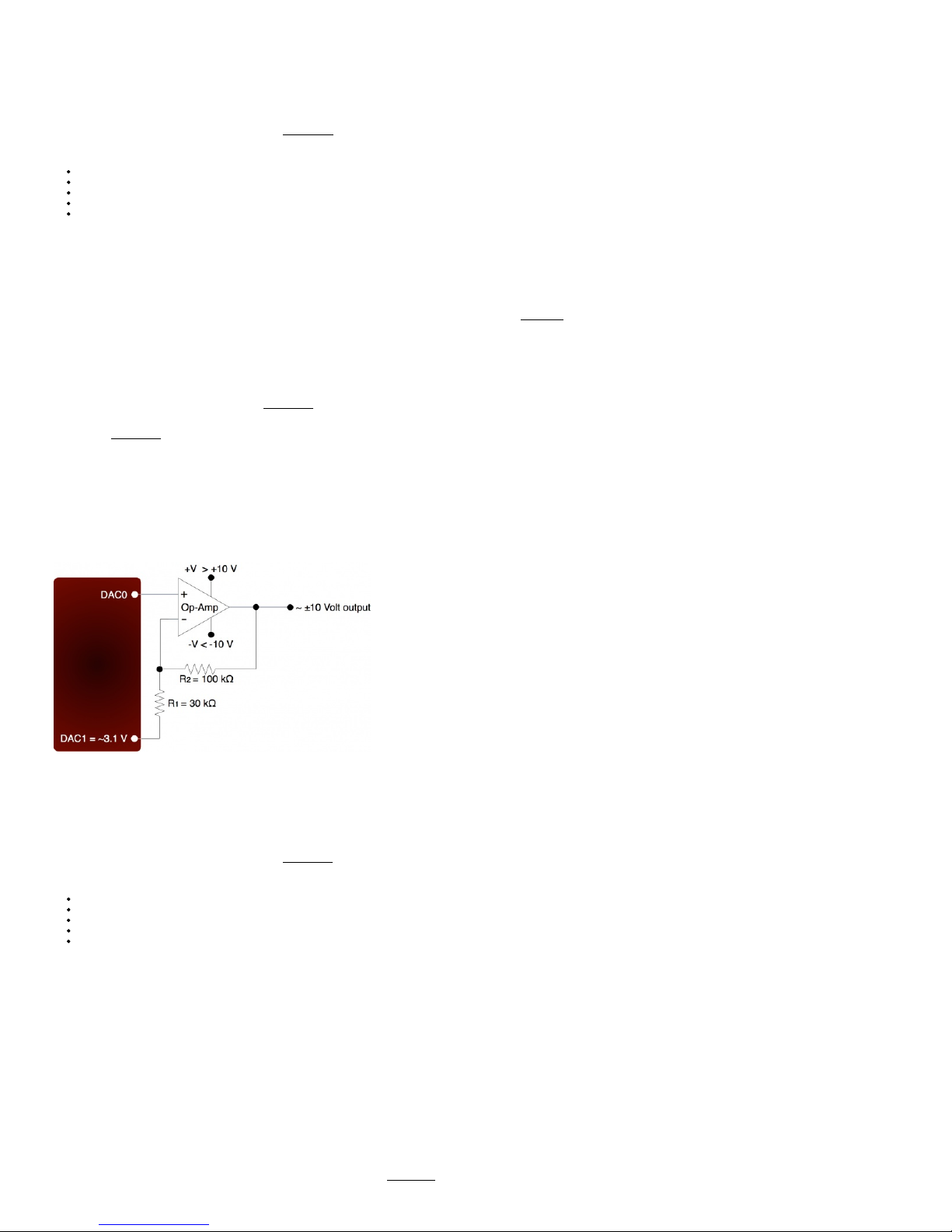
2.7.1.2 - Different Output Ranges
See the end of thi s section for information about the LJTick-D AC which has a +/-10V range.
The typical output range of the DACs is about 0.04 to 4.95 volts. For other unipolar ranges, an op-amp in the non-inverting
configuration (Figure 2.6-1) ca n be used to provi de the desired gain. For e xample, to increase the maximum output from 4.95 volts
to 10.0 volts, a gain of 2.02 is requi red. If R2 (in Figure 2-3) is chosen as 100 kΩ, then an R1 of 97.6 kΩ is the clo sest 1% resistor
that provides a gain greater than 2.02. The +V supply for the op-amp would have to be greater than 10 volts.
For bipolar output ranges, such as ±10 volts, a similar op-amp circuit can be used to provide gain and offset, but of course the opamp must be powered with supplies greater than the d esired output range (depending on the ability of the op-amp to drive it’s
outputs close to the power rai ls). If ±10, ±12, or ±15 volt supplies are available, consi der using the LT1490A op-amp (linear.com),
which can handle a supply span up to 44 volts.
A reference voltage is also required to provide the offset. In the following circuit, D AC1 is used to provide a reference voltage. The
actual value of DAC1 can be adjusted such that the circuit output is 0 volts at the DAC0 mid-scale voltage, and the value of R1 can
be adjusted to get the desired gain. A fixed reference (such as 2.5 volts) could also be used instead of DAC1.
Figure 2.7-1. ±10 Volt DAC Output Circuit
A two-point calibration should be done to determine the exact i nput/output relationship of this circuit. Refer to application note
SLOA097 from ti.com for further information about gain and offset design with op-amps.
LJTick-DAC:
There is an accessory available from LabJack called the LJTi ck-DAC that provides a pair of 14-bit analog outputs with a range of
±10 volts. The LJTick-DAC plugs into any digital I/O block, and thus up to 10 of these can be used per U3 to add 20 analog
outputs. The LJTick-DAC has various improvements compared to the built-in DACs on the U3:
Range of +10.0 to -10.0 volts.
Resolution of 14-bits.
Slew rate of 0.1 V/μs.
Based on a reference , rather than regulator, so more accurate and stable.
Does not affect analog inputs in any configura tion.
2.8 - Digital I/O
The LabJack U3 has up to 20 digital I/O channels. 16 are available from the flexible I/O lines, and 4 dedicated digital I/O (CIO0CIO3) are available on the DB15 connector. The first 4 lines, FIO0-FIO3, are unavailable on the U3-HV. Each digital line can be
individually configured as input, output-high, or output-low. The digital I/O use 3.3 volt logic and are 5 volt tolerant.
The LabJackUD driver uses the following bit numbers to specify all the di gital lines:
0-7 FIO0-FIO 7 (0-3 unavail able on U3-HV)
8-15 EIO0-EIO 7
16-19 CIO0-CIO 3
The 8 FIO lines appear on the built-in screw-terminals, while the 8 EIO and 4 CIO li nes appear only on the DB15 connector. See
the DB15 Section of this User’ s Guide for more information.
All the digital I/O include an internal series resistor that provi des overvoltage/short-circuit protection. These series resistors also
limit the ability of these lines to sink or source current. Refer to the speci fications in Appendix A .
12
Page 13
All digital I/O on the U3 have 3 possible states: input, output-hig h, or output-low. Each bit of I/O can be configured individually.
When configured as an input, a bit has a ~100 kΩ pull-up resistor to 3.3 volts (all digital I/O are 5 volt tolerant). When configured as
output-high, a bit is connected to the internal 3.3 volt supply (through a series resistor). When configured as output-low, a bit is
connected to GND (through a series resistor).
The fact that the digital I/O are specified as 5-volt tole rant means that 5 volts can be connected to a digital input without problems
(see the actual li mits in the speci fications in Appendix A). If 5 volts i s needed from a digital output, consider the following solutions:
In some cases, an open-collector style output can be used to get a 5V signal. To g et a low set the line to output-low, and to
get a high set the line to input. When the line is set to input, the voltage on the line is determined by a pull-up resistor. The
U3 has an internal ~100k resistor to 3.3V, but an external resistor can be added to a different voltage. Whether this will work
depends on how much current the load is going to draw and what the required logic thresholds are. Say for example a 10k
resistor is added from EIO0 to VS. EIO0 ha s an internal 100k pull-up to 3.3 volts and a series output resistance of about 180
ohms. Assume the load draws just a few microamps or less and thus is negligible. When EIO0 is set to input, there will be
100k to 3.3 volts in p arallel with 10k to 5 volts, and thus the line wi ll sit at about 4.85 volts. When the line is set to output-low,
there wi ll be 180 ohms in series with the 10k, so the line will be pulled down to about 0.1 volts.
The surefire way to get 5 volts from a digital output is to add a simple logic buffer IC that is powered by 5 volts and
recognizes 3.3 volts as a high input. Consider the CD74ACT541E from TI (or the inverti ng CD74ACT540E). All that is
needed is a few wi res to bring VS, GND, and the signal from the LabJack to the chip. This chip can level shi ft up to eight
0/3.3 volt signals to 0/5 vo lt signals and provi des high output drive current (+/-24 mA).
Note that the 2 DAC channe ls on the U3 can be set to 5 volts, providing 2 output lines with such capability.
The power-up condition of the digital I/O can be configured by the user with the "Config Defaults" option in LJControlP anel. F rom
the factory, all digital I/O are configured to power-up as inputs. Note that even if the power-up default for a line is changed to
output-high or output-low, there is a delay of a bout 5 ms at power-up where all digital I/O are in the factory default condition.
If you want a floating digital input to read low, an external pull-down resistor can be added to overpower the internal 100k pull-up.
4.7k to 22k would be a typical range for thi s pull-down, with 10k being a solid choice for most applications.
The low-level Feedback function (Section 5.2.5) writes and reads all digital I/O. For information about usi ng digital I/O under the
Windows LabJackUD driver, see Section 4.3.5. See Section 3.1 for timi ng information.
Many function parameters contain specific bits within a single integer parameter to write/read specific information. In particular,
most digital I/O parameters contain the information fo r each bit of I/O in one integer, where each bit of I/O corresponds to the same
bit in the parameter (e.g. the direction of FIO0 is set in bit 0 of parameter FIOD ir). For instance, in the low-level function ConfigU3,
the parameter FIODirection is a single byte (8 bits) that writes/reads the power-up direction of each of the 8 FIO lines:
if FIODirection is 0, all FIO lines are input,
if FIODirection is 1 (20), FIO0 is output, FIO1-FIO7 are input,
if FIODirection is 5 (20 + 22), FIO0 and FIO2 are output, all other FIO lines are input,
if FIODirection is 255 (20 + … + 27), FIO0-FIO7 are output.
2.8.1 - Typical Digital I/O Connections
2.8.1.1 - Input: Driven Signals
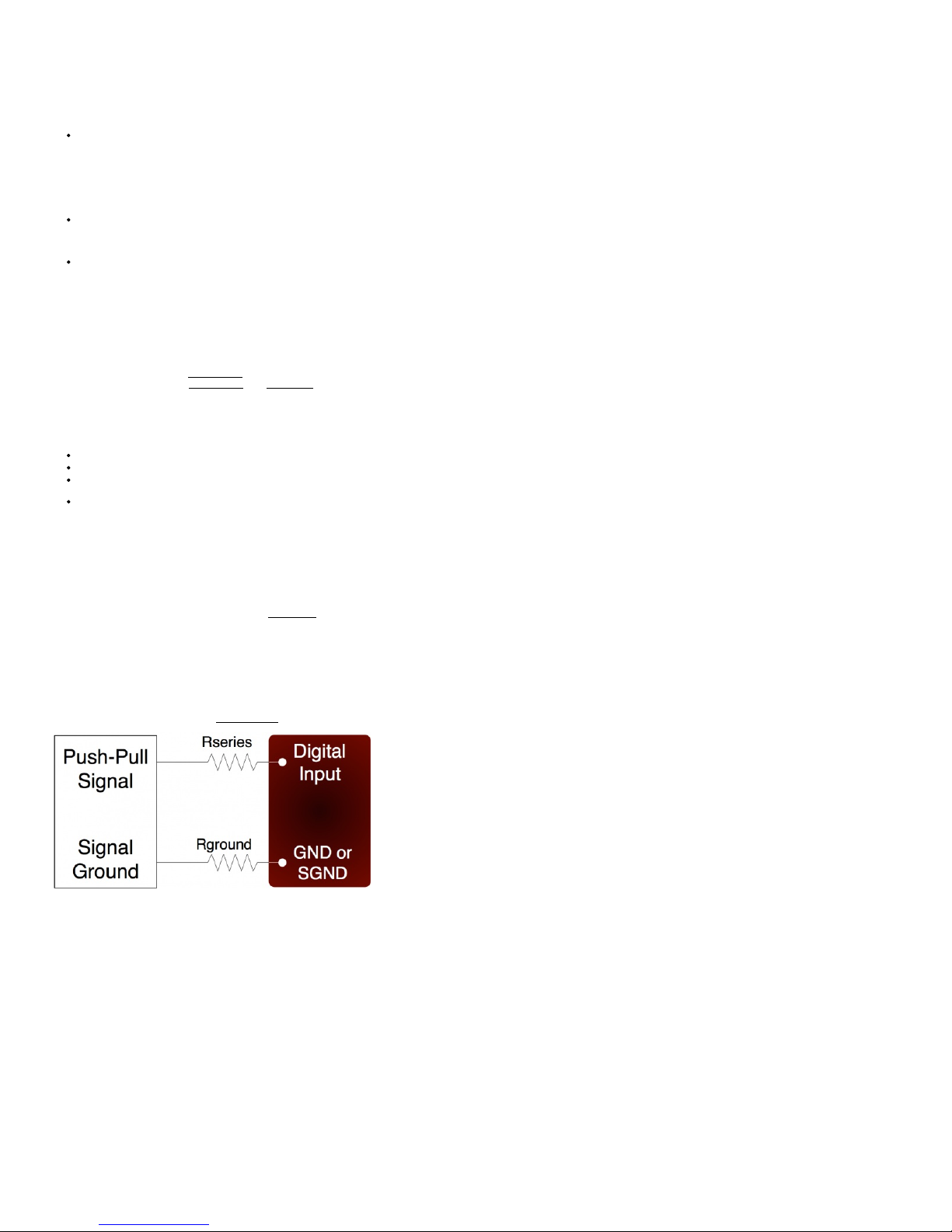
The most basic connection to a U3 digital input i s a driven si gnal, often called push-pull. With a push-pull signal the source is
typically providing a high voltage for logic high and zero volts for logic low. Thi s signal is generally connected directly to the U3
digital input, considering the voltage specifications in Appendix A . If the sig nal is over 5 volts, it can still be connected with a series
resistor. The digital inputs have protective devices that clamp the voltage at GND and VS, so the series resistor is used to limit the
current through these protective devices. For instance, i f a 24 volt signal is connected through a 22 kΩ series resistor, a bout 19
volts will be dropped across the resistor, resulting in a current of 0.9 mA, which is no problem for the U3. The series resistor should
be 22 kΩ or less, to make sure the voltage on the I/O line when low is pulled below 0.8 volts.
The other possible consideration with the basic push-pull signal is the ground connection. If the signal is known to already have a
common ground with the U3, then no additional ground connection is used. If the signal is known to not have a common ground
with the U3, then the signal ground can simply be connected to U3 GND . If there is uncertainty about the relationship between
signal ground and U3 ground (e.g. possible common ground through AC mains), then a ground connection with a ~10 Ω series
resistor is generally recommended (see Section 2.6.3.4).
Figure 2.8-1. Driven Si gnal Connection To Digital Input
Figure 2.8-1 shows typical connections. Rground is typically 0-100 Ω. Rseries is typically 0 Ω (short-circuit) for 3.3/5 volt logic, or
22 kΩ (max) for hi gh-voltage logic. Note that an individual ground connection is often not needed for every signal. Any si gnals
powered by the same external supply, or otherwise referred to the same external ground, should share a sing le ground connection
to the U3 if possible.
When dealing with a new sensor, a push-pull signal is often incorrectly assumed when in fact the sensor provi des an open-collector
signal as described next.
2.8.1.2 - Input: Open-Collector Signals
Open-collector (also called open-drain o r NPN) is a very common type of digital signal. Rather than providing 5 volts and ground,
like the push-pull signal, an open-collector signal provides ground and hi gh-impedance. This type of signal can be thought of as a
switch connected to ground. Since the U3 digital inputs have a 100 kΩ internal pull-up resistor, an open-collector signal can
generally be connected directly to the input. When the signal is inactive, it is not drivi ng any voltage and the pull-up resistor pulls the
digital input to logic high. When the signal is active, it drives 0 volts which overpowers the pull-up and pulls the digital input to logic
low. Sometimes, an external pull-up (e.g. 4.7 kΩ from Vs to digital input) will be installed to increase the strength and speed of the
logic high condition.
13
Page 14
Figure 2.8-2. Open-Collector (NPN) Connection To Digital Input
Figure 2.8-2 shows typical connections. Rground is typically 0-100 Ω, Rseries is typically 0 Ω, and Rpullup, the external pull-up
resistor, is generally not required. If there is some uncertainty about whethe r the signal is really open-collector or could drive a
voltage beyond 5.8 volts, use an Rseries of 22 kΩ as discussed in Section 2.8.1.1, and the input should be compatible with an
open-collector si gnal or a driven signal up to at least 48 volts.
Without the optional resistors, the figure simplifies to:
Figure 2.8-3. Simplified Open-Collector (NPN) Connection To Digital Input Without Optional Re sistors
Note that an individual ground connection i s often not needed for every signal. Any signals powered by the same external supply,
or otherwi se referred to the same external ground, should share a single ground connection to the U3 if possible.
2.8.1.3 - Input: Mechanical Switch Closure
To detect whether a mechanical switch (dry contact) is open or closed, connect one side of the swi tch to U3 ground and the other
side to a digital input. The behavior is very similar to the open-collector described above.
Figure 2.8-4. Basic Mechani cal Switch Connection To Digital Input
When the switch is open, the internal 100 kΩ pull-up resistor will p ull the digital input to about 3.3 volts (logic high). When the switch
is closed, the ground connection will overpower the pull-up resistor and pull the digital input to 0 volts (lo gic low). Since the
mechanical swi tch does not have any electrical connections, besides to the LabJack, it can safely be connected directly to GND,
without using a series resistor or SGND.
When the mechanical switch is closed (and even perhaps when opened), it will bounce briefly and produce multiple electrical
edges rather than a single hi gh/low transition. For many basic digi tal input applications, this is not a problem as the software can
simply poll the input a few ti mes in succession to make sure the measured state is the steady state and not a bounce . For
applications using ti mers or counters, however, this usually is a problem. The hardware counters, for instance, are very fast and will
increment on all the bounces. Some solutions to this issue are:
Software Debounce: If it is known that a real closure cannot occur more than once per some interval, then software can be
used to li mit the number of counts to that rate.
Firmware Debounce: See Section 2.9.1 for information about timer mode 6.
Active Hardware Debounce: Integrated circuits are avai lable to debounce switch signals. This is the most reliable hardware
solution. See the MAX6816 (maxim-ic.com) or EDE2008 (elabinc.com).
Passive Hardware Debounce: A combinati on of resistors and capacitors can be used to debounce a signal. Thi s is not
foolproof, but works fine in most applications.
14
Page 15
Figure 2.8-5. Passive Hardware Debounce
Figure 2.8-5 shows one possible confi guration for passi ve ha rdware debounce. First, consi der the case where the 1 kΩ resistor is
replaced by a short circuit. When the switch closes it immediately charges the capacitor and the digital input sees logic low, but
when the switch opens the capacitor slowly discharges through the 22 kΩ resistor with a time constant of 22 ms. B y the time the
capacitor has discharged enough for the d igital input to see logic high, the mechani cal bouncing is done. The main purpose of the
1 kΩ resistor is to limit the current surge when the switch is clo sed. 1 kΩ limits the maxi mum current to about 5 mA, but better
results might be obtained with smaller resistor values.
2.8.1.4 - Output: Controlling Relays
All the digital I/O lines have serie s resistance that restricts the amount of current they can sink or source, but solid-state relays
(SSRs) can usually be controlled directly by the digital I/O. The SSR is connected as shown in the following diagram, where VS (~5
volts) connects to the positive control input and the digital I/O line connects to the negative control i nput (sinking config uration).
Figure 2.8-6. Relay Connections (Sinking Control, High-Side Load Switching)
When the digital line is set to output-low, control current flows and the relay turns on. When the digital line is set to input, control
current does not flow a nd the relay turns off. Whe n the digital line is set to output-high, some current flows, but whether the relay is
on or off depends on the specifications of a particular relay. It is recommended to only use output-low and input.
For example, the Series 1 (D12/D24) or Series T (TD12/TD24) relays from Crydom specify a max turn-on of 3.0 volts, a min turnoff of 1.0 volts, and a nominal input impedance of 1500 Ω.
When the digital line is set to output-low, it is the equivalent of a ground connection wi th 180 Ω (EIO/CIO) or 550 Ω (FIO) in
series. When using an EIO/CIO line, the resulting voltage across the control inputs of the relay will be about
5*1500/(1500+180) = 4.5 volts (the other 0.5 volts is dropped across the internal resistance of the EIO/CIO line). With an FIO
line the voltage across the inputs of the relay will b e about 5*1500/(1500+550) = 3 .7 volts (the other 1.3 vo lts are dropped
across the internal resistance of the FIO line). Both of these are well above the 3.0 volt threshold for the relay, so it will turn on.
When the digital line is set to input, it is the equivalent of a 3.3 volt connection with 100 kΩ in series. The resulting vo ltage
across the control inputs of the relay will be close to zero, as vi rtually all of the 1.7 volt difference (between VS and 3.3) is
dropped across the internal 100 kΩ resistance. This is well below the 1.0 volt threshold for the relay, so it will turn off.
When the digital line is set to output-high, it is the equivalent of a 3.3 volt connection with 180 Ω (EIO/C IO) or 550 Ω (FIO) in
series. When using an EIO/CIO line, the resulting voltage across the control inputs of the relay will be about
1.7*1500/(1500+180) = 1.5 volts. With an FIO line the voltage across the inputs of the relay will be about
1.7*1500/(1500+550) = 1.2 volts. Both of these in the 1.0-3.0 volt region that is not defined for these example relays, so the
resulting state is unknown.
Note that sinking excessive current i nto digital outputs can cause noticeable shifts in analog input readings. For example, the FIO
sinking configuration above sinks about 2 .4 mA into the dig ital output to turn the SSR on, whi ch could cause a shift of roughly 1 mV
to analog input readings.
Mechanical relays require more control current than SSRs, and cannot be controlled directly by the digital I/O on the U3 . To control
higher currents with the digital I/O, some sort of buffer is used. S ome options are a discrete transistor (e.g. 2N2222), a specific
chip (e.g. ULN2003), or an op-amp.
Note that the U3 DACs can source enough current to contro l almost any SSR and even some mechanical relays, and thus can be
a convenient way to control 1 or 2 relays. With the DA Cs you would typically use a sourcing configuration (DAC/GND) rather than
sinking (VS/DAC).
The RB12 relay board is a useful accessory available from LabJack. This board connects to the DB15 connector on the U3 and
accepts up to 12 industry standard I/O modules (designed for Opto22 G4 modules and similar).
Another a ccessory available from LabJack is the LJTick-RelayDriver. This is a two channel module that plugs into the U3 screwterminals, and allows two digital lines to each hold off up to 50 volts and sink up to 200 mA. This allows control of virtua lly any solidstate or mechanical relay.
2.9 - Timers/Counters
The U3 has 2 timers (Timer0-Timer1) and 2 counters (Counter0-Counter1). When any of these timers or counters are enabled, they
take over an FIO/EIO line in sequence (Timer0, Timer1, Counter0, then Counter1), starting with FIO0+TimerCounterPinOffset.
Some examples:
1 Timer enabled, Counter0 disabled, Counter1 disabled, and Ti merCounterPinOffset=4:
FIO4=Timer0
15
Page 16

1 Timer enabled, Counter0 disabled, Counter1 enabled, and TimerCounterPinOffset=6:
FIO6=Timer0
FIO7=Counter1
2 Timers enabled, Counter0 enabled, Counter1 enabled, and TimerCounterPinOffset=8:
EIO0=Timer0
EIO1=Timer1
EIO2=Counter0
EIO3=Counter1
Starting with hardware revision 1.30, timers/counters cannot appear on FIO0-3, and thus TimerCou nterPinOffset must be 4-8.
A value of 0-3 will result in an error. This error can be suppressed by a power-up default setting in LJControlPanel. If suppressed, a
0-3 will result i n an offset of 4.
Timers and counters can appear on vario us pins, but other I/O lines never move. For example, Timer1 can appear anywhere from
FIO4 to EIO1 , depending on TimerCounterPinOffset and whether Timer0 is enabled. On the other hand, FIO5 (for example), i s
always on the screw terminal labeled FIO5, and AIN5 (if enabled) is always on that same screw termina l.
Note that Counter0 is not available with certain timer clock base frequencies. In such a case, it does not use an external FIO/EIO
pin. An error will result if an attempt is made to enable Counter0 when one of these fre quencies is configured. Similarly, an error
will result if an atte mpt is made to configure one of these frequencies when Co unter0 is enabled.
Applicable digital I/O are automatically configured as input o r output as neede d when timers and counters are ena bled, and stay
that way when the timers/counters are disabled.
See Section 2.8.1 for information about signal connections.
Each counter (Counter0 or Counter1) consists of a 32-bit register that accumulates the number of falling edges detected on the
external pin. If a counter is reset and read in the same function call, the read returns the value just be fore the reset.
The timers (Timer0-Timer1) have various modes available:
Index (Low-level & UD)
0
16-bit PWM output
1
8-bit PWM output
2
Period input (32-bit, rising edges)
3
Period input (32-bit, falling edges)
4
Duty cy cle input
5
Firmware counter input
6
Firmware counter input (with debounce)
7
Frequency output
8
Quadrature input
9
Timer stop input (odd timers only)
10
System time r low rea d (default mo de)
11
Syst em timer hight read
12
Period input (16-bit, rising edges)
13
Period input (16-bit, falling edges)
Table 2. 9-1. U3 Time r Modes
Both timers use the same timer c lock.
There are 7 choices for the timer cl ock base:
Index (Low-level/UD)
0/20
4 MHz
1/21
12 MHz
2/22
48 MHz (default)
3/23
1 MHz /Divisor
4/24
4 MHz /Divisor
5/25
12 MHz /Divisor
6/26
48 MHz /Divisor
Table 2. 9-2. U3 Time r Clock Base Options
Note that these clocks apply to the U3 hardware revi sion 1.21+. With hardware revision 1.20 all clocks are half of the values
above.
The first 3 clocks have a fixed frequency, and are not affected by TimerClockDivisor. The frequency of the last 4 clocks can be
further adjusted by Ti merClockDivisor, but when usi ng these clocks Counter0 is not available. When Counter0 is not available, it
does not use an external FIO/EIO pin. The divi sor has a range of 0-255, where 0 corresponds to a divi sion of 256.
Note that the DACs (Section 2.7) are derived from PWM signals that are affected by the timer clock frequency. The default timer
clock frequency of the U3 is set to 48 MHz, as this results in the minimum DAC output noise. If the frequency is lowered, the DACs
will have more noise, where the frequency of the noise is the ti mer clock frequency di vided by 216.
2.9.1 - Timer Mode Descriptions
2.9.1.1 - PWM Output (16-Bit, Mode 0)
Outputs a pulse width modulate d rectangular wave output. Value passed should be 0-65535, and determines what portion of the
total time is spent low (out of 65536 total i ncrements). That means the duty cycle can be varied from 100% (0 out of 65536 are low)
to 0.0015% (65535 out of 65536 are low).
The overall frequency of the PWM output is the clock frequency specified by TimerClockBase/TimerClockDivisor divided by 216.
The following table shows the range of a vailable PWM frequencies based on timer clock setti ngs.
PWM16 Frequency Ranges
TimerClockBase
Divisor=1
Divisor=256
0
4 MHz
61.04
N/A112 MHz
183.11
N/A248 MHz (default)
732.42
N/A
3
1 MHz /Divisor
15.26
0.06
4
4 MHz /Divisor
61.04
0.238
5
12 MHz /Divisor
183.11
0.715
6
48 MHz /Divisor
732.42
2.861
Table 2. 9.1.1-1. 16-bit PW M Frequencie s
Note that the clocks above apply to the U3 hardware revision 1.21. With hardware revision 1.20 all clocks are half of those values.
The same clock applies to all timers, so all 16-bit PWM channels will have the same frequency and will have their falling edges at
the same ti me.
PWM output starts by setti ng the di gital line to output-low for the specified amount of time. The o utput does not necessarily start
instantly, but rather waits for the internal clock to roll. For example, if the PWM frequency i s 100 Hz, that means the period is 10
milliseconds, and thus after the command is received by the device it could be anywhere from 0 to 1 0 milliseconds before the start
of the PWM output.
16
Page 17

of the PWM output.
If a duty cycle of 0.0% (totally off) is required, consider using a simple inverter IC such as the CD 74ACT540E from TI. Or you can
switch the mode of the ti mer to some input mode, a nd add an external pull-down to hold the line low when set to input.
2.9.1.2 - PWM Output (8-Bit, Mode 1)
Outputs a pulse width modulate d rectangular wave output. Value passed should be 0-65535, and determines what portion of the
total time is spent low (out of 65536 total i ncrements). The lower byte is actually ignored since this is 8-bit PWM. Tha t means the
duty cycle can be varied from 100% (0 out of 65536 are low) to 0.4% (65280 out of 65536 are low).
The overall frequency of the PWM output is the clock frequency specified by TimerClockBase/TimerClockDivisor divided by 28.
The following table shows the range of a vailable PWM frequencies based on timer clock setti ngs.
PWM8 F requency Ranges
TimerClockBase
Divisor=1
Divisor=256
0
4 MHz
15625
N/A112 MHz
46875
N/A248 MHz (default)
187500
N/A31 MHz /Divisor
3906.25
15.259
4
4 MHz /Divisor
15625
61.035
5
12 MHz /Divisor
46875
183.105
6
48 MHz /Divisor
187500
732.422
Table 2. 9.1.2-1. 8-bit PW M Frequencie s
Note that the clocks above apply to the U3 hardware revision 1.21. With hardware revision 1.20 all clocks are half of those values.
The same clock applies to all timers, so all 8-bit PWM channels will have the same frequency and will have their falling edges at
the same ti me.
PWM output starts by setti ng the di gital line to output-low for the specified amount of time. The o utput does not necessarily start
instantly, but rather waits for the internal clock to roll. For example, if the PWM frequency i s 100 Hz, that means the period is 10
milliseconds, and thus after the command is received by the device it could be anywhere from 0 to 1 0 milliseconds before the start
of the PWM output.
If a duty cycle of 0.0% (totally off) is required, consider using a simple inverter IC such as the CD 74ACT540E from TI. Or you can
switch the mode of the ti mer to some input mode, a nd add an external pull-down to hold the line low when set to input.
2.9.1.3 - Period Measurement (32-Bit, Modes 2 & 3)
Mode 2: On every rising edge seen by the external pin, thi s mode records the number of clock cycles (clock freque ncy determined
by TimerClockBa se/TimerClockDivisor) between this risi ng edge and the previous rising edge. The value is updated on every
rising edge, so a read returns the ti me between the most recent pair of rising edges.
In this 32-bit mode, the processor must jump to an i nterrupt service routine to record the time, so small errors can occur if another
interrup t is already in progress. The possible error sources are:
Other edge interrupt timer modes (2/3/4/5/8/9/12/13). If an interrupt is already being handled due to an edge on the other
timer, delays of a few microseconds are possible.
If a stream is in progress, every sample is acquired in a hi gh-priority interrupt. These interrupts could cause delays on the
order of 10 microseconds.
The always active U3 system timer causes an i nterrupt 61 times per second. If this interrupt happens to be in progress when
the edge occurs, a delay of about 1 microsecond is possible. If the software watchdog is enabled, the system timer interrupt
takes longer to execute and a delay of a few microseconds is possible.
Note that the minimum measurable period is limited by the edge rate limit discussed in Section 2.9.2.
See Section 3.2.1 for a special condition if stream mode is used to acquire timer data in this mode.
Writing a value of zero to the timer performs a reset. After reset, a read of the timer value will return zero until a new edge is
detected. If a timer is reset and read in the same function call, the read returns the value just before the reset.
Mode 3 is the same except that falling edges are used instead of rising edges.
2.9.1.4 - Duty Cycle Measurement (Mode 4)
Records the high and low time of a signal on the external pin, which provi des the duty cycle, pulse width, and period of the signal.
Returns 4 bytes, where the first two bytes (least significant word or LSW) are a 16-bit value representing the number of clock ticks
during the hi gh signal, and the second two bytes (most significant word or MSW) are a 16-bit value representing the number of
clock ticks during the low signal. The clock frequency is determined by TimerClockBase/TimerClockDivisor.
The appropriate value is updated on every edge, so a read returns the most recent high/low times. Note that a duty cycle of 0% or
100% does not have any edges.
To select a clock frequency, consider the longest expected high or low time, and set the clock freque ncy such that the 16-bit
registers will not overflow.
Note that the minimum measurable high/lo w time is limited by the edge rate limit discussed in Section 2.9.2.
When using the LabJackUD driver the value re turned is the entire 32-bit value. To determine the high and low time this value
should be split into a high and low word. One way to do this is to do a modulus divide by 216 to determine the LSW, and a normal
divide by 216 (keep the quotient and discard the remainder) to determine the MSW.
Writing a value of zero to the timer performs a reset. After reset, a read of the timer value will return zero until a new edge is
detected. If a timer is reset and read in the same function call, the read returns the value just before the reset. The d uty cycle reset
is special, in that if the signal is low at the time of reset, the high-time/lo w-time registers are set to 0/65535, but if the signal i s high
at the time of reset, the high-time/low-time registers are set to 65535/0. Thus if no edges occur before the next read, it is possible
to tell if the duty cycle is 0% or 100%.
2.9.1.5 - Firmware Counter Input (Mode 5)
On every rising edge seen by the externa l pin, this mode increments a 32-bit register. Unlike the pure hardware counters, these
timer counters require that the fi rmware jump to an interrupt service routine on each edge.
Writing a value of zero to the timer performs a reset. After reset, a read of the timer value will return zero until a new edge is
detected. If a timer is reset and read in the same function call, the read returns the value just before the reset.
2.9.1.6 - Firmware Counter Input With Debounce (Mode 6)
17
Page 18

Intended for frequenci es less than 10 Hz, this mode adds a debounce feature to the firmware counter, which is particularly useful
for signals from mechanical switches. On every applicab le edge seen by the external pin, this mode increments a 32-bit register.
Unlike the pure hardware counters, these timer counters re quire that the firmware jump to an interrupt service routine on each
edge.
The debounce period is set by writing the timer value. The low byte of the timer value is a number from 0-255 that specifies a
debounce period in 16 ms increments (plus an extra 0-16 ms of variability):
Debounce Period = (0-16 ms) + (TimerValue * 16 ms)
In the high byte (bits 8-16) of the timer value, bit 0 determines whether negative edges (bit 0 clear) or positive edges (bit 0 set) are
counted.
Assume thi s mode is enabled with a value of 1, meaning that the debounce period is 16-32 ms and negative edges will be
counted. When the input detects a ne gative edge, it increments the count by 1, and then waits 16-32 ms before re-arming the edge
detector. Any negative edges within the debounce period are ignored. This is good behavior for a normally-high signal where the
switch closure causes a brief low signal (Figure 2-10). The debounce period can be set long enough so that bouncing on both the
switch closure and switch open is ignored.
Writing a value of zero to the timer performs a reset. After reset, a read of the timer value will return zero until a new edge is
detected. If a timer is reset and read in the same function call, the read returns the value just before the reset.
2.9.1.7 - Frequency Output (Mode 7)
Outputs a square wave at a frequency determined by TimerClockBase/TimerClockDivisor divided by 2*Timer#Value. The Value
passed should be between 0-255, where 0 i s a divisor of 256. By changing the clock configuration and timer value, a wide range
of frequencies can be output, as shown in the following table:
Mode 7 Frequency Ranges
Divisor=1
Divisor=1
TimerClockBase
Value=1
Value=256
0
4 MHz
2000000
7812.5
1
12 MHz
6000000
23437.5
2
48 MHz (default)
24000000
93750
Divisor=1
Divisor=256
Value=1
Value=256
3
1 MHz /Divisor
500000
7.629
4
4 MHz /Divisor
2000000
30.518
5
12 MHz /Divisor
6000000
91.553
6
48 MHz /Divisor
24000000
366.211
Table 2. 9.1.7-1. Mode 7 Frequency Ra nges
Note that the clocks above apply to the U3 hardware revision 1.21. With hardware revision 1.20 all clocks are half of those values.
The frequency output has a -3 dB frequency of about 10 MHz on the FIO lines. Accordingly, at high frequencies the output
waveform will get less square and the amplitude will decrease.
The output does not necessarily start instantly, but rather waits for the internal clock to roll. For example, i f the output frequency is
100 Hz, that means the period is 10 milliseconds, and thus after the command is received by the device it could be anywhere from
0 to 10 milliseconds before the start of the frequency output.
Frequency List for U3 Timer Mode 7
CSV list of the 262,144 possible frequency output options on the U3 hardware rev 1.21+. Columns are Hz, base clock, clock
divisor, and timer value. Oct 27, 2008.
File attachment:
U3_FreqOutList_Hz_B ase_Divisor_Value.csv
2.9.1.8 - Quadrature Input (Mode 8)
Requires both timers, where Timer0 will be quadrature channel A, and Timer1 will be quadrature channel B. The U3 does 4x
quadrature counting, and returns the current count as a signed 32-bit integer (2’s complement). The same current count is returned
on both timer value parameters.
Writing a value of zero to either or both ti mers performs a reset of both. After reset, a read of either timer value will return zero until
a new quadrature count is detected. If a timer is reset and read in the same functi on call, the read returns the va lue just before the
reset.
4X Counting
Quadrature mode uses the very common 4X counting method, which p rovides the highest resolution possible. That means you get
a count for every edge (rising & falling) on both phases (A & B). Thus if you have an encod er that provides 32 PPR, and you rotate
that encoder forward 1 turn, the ti mer Value register will be incremented by +128 counts.
Z-phase support
Quadrature mode supports Z-Phase. When enabled this feature will set the count to zero when the specified IO line sees a logic
high.
Z-phase is controlled by the value wri tten to the timer during initialization. To enable z-phase support set bit 15 to 1 and set bits 0
through 4 to the DIO number that Z is connected to. E G: for a Z-li ne on E IO3 set the timer value to 0x800B or 32779. This value
should be sent to both the A and B timers.
Note that the LabJack will only check Z when it sees an edge on A or B.
Z-phase support requi res Firmware 1.30 or later.
2's Complement
Other timer modes return unsigned values, but this timer mode is uni que in that it returns a signed value from -2147483648 to
+2147483647. That i s, a 32-bit 2's complement value. When you do a timer value read and get back a single float from the UD
driver, the math is already done and you get back a value from -2147483648.0 to +2147483647.0, but when using the speci al
channels 20x/23x/224 you get the LSW and MSW separately and have to do the math yourself. Search for 2's complement math
for your particular programming language.
In a language such as C++, you start by doing using unsi gned 32-bit variables & constants to compute Value = (MSW * 65536) +
LSW. Then simply cast Value to a signed 32-bit integer.
In a language such as Java that does not support unsigned inte gers, do everythi ng with signed 64-bit variables & constants. First
calculate Value = (MSW * 65536) + LSW. If Value < 2147483648, you are done. If Value >= 2147483648, do ActualValue = -1 *
(4294967296 - Value).
18
Page 19

2.9.1.9 - Timer Stop Input (Mode 9)
This mode should only be assi gned to Timer1. On every rising edge seen by the external pin, this mode increments a 16-bit
register. When that register matches the specified timer value (stop count value), Timer0 is stopped. The range for the stop count
value is 1-65535. Gene rally, the signal applied to Timer1 is from Timer0, which is configured in some output timer mode. One
place where this might be useful is for stepper motors, allowing control over a certain number of steps.
Note that the timer is counting from the external pin like other input timer modes, so you must connect something to the stop timer
input pin. For example, if you are using Timer1 to stop Timer0 which is outputting pulses, you must connect a jumper from Ti mer0
to Ti mer1.
Once this timer reache s the specified stop count value, and stops the adjacent timer, the timers must be reconfigured to restart the
output.
When Timer0 is stopped, it is still enabled but just not outputting anything. Thus rather than returni ng to whatever previous digital
I/O state was on that terminal, i t goes to the state "digi tal-input" (which has a 100 kΩ pull-up to 3.3 volts). That means the best
results are generally obtained if the terminal used by Timer0 was initially configured as digital input (factory default), rather than
output-high or output-low. Thi s will result i n negative going pulse s, so if you need positive going pulses consider using a simple
inverter IC such as the CD74ACT540E from TI.
The MSW of the read from this timer mode returns the number of edges counted, but does not increment past the stop count value.
The LSW of the read returns edges waiting for.
2.9.1.10 - System Timer Low/High Read (Modes 10 & 11)
The LabJack U3 has a free-running internal 64-bit system timer with a frequency of 4 MHz. Timer modes 10 & 11 return the lower
or upper 32-bits of this timer. An FIO line is allocated for these modes like normal, even though they are internal readings and do
not require any external connections. This system ti mer cannot be reset, and is not affected by the timer clock.
If using both modes 10 & 11, read both in the same low-level command and read 10 before 11.
Mode 11, the upper 32 bits of the system timer, is not available for stream reads. Note that when streami ng on the U3, the timing is
known anyway (elapsed time = scan rate * scan number) and it does not make sense to stream the system timer modes 10 or 11.
Note that system timer runs at 2MHz on U3 hardware 1.20.
2.9.1.11 - Period Measurement (16-Bit, Modes 12 & 13)
Similar to the 32-bit edge-to-edge timing modes described above (modes 2 & 3), except that hardware capture registers are
used to record the edge times. This limits the ti mes to 16-bit values, but is accurate to the resolution of the clock, and not subject to
any e rrors due to firmware processing delays.
Note that the minimum measurable period is limited by the edge rate limit discussed in Section 2.9.2.
2.9.1.12 - Line-to-Line Measurement (Mode 14)
This timer mode requires firmwa re 1.30 or la ter.
Introduction:
The Line-to-Line timer mode uses two timers to measure the time between specified edges on two different li nes. For instance,
you can measure the time between a rising edge on Timer0 and a falling edge on Timer1. When the LabJack sees the specified
edge on Timer0 it starts counting until it se es the specified edge on Timer1. Hig h resolution up to 20.8ns can be achieved with this
mode.
Configuring:
To configure a LabJack for Line-to-Line mode set an even timer and the next (odd) timer to mode 14. The timer values determine
the edge that the timer wi ll respond to, 1 being rising, 0 being falling. So, if Ti mer0's value is 0 and Timer1's is 1 then the LabJack
will measure the time between a falling edge on Timer0 to a rising edge on Timer1.
Readings:
Once configured the timer will return zero until both specified edges have been detected. The time difference in TimerClock
periods is then returned by both timers unti l they are reset. Both timers will return the same reading, so it is only necessary to read
one or the other. To convert to time, divide the value re turned by the timer clock. This mode returns 16-bit values, so care should be
taken to be sure that the specified condition does not exceed the maximum time. The maximum time can be calculated by (2^16-
1)/Ti merClock.
Resetting:
Once a measurement has been acquired the even timer ne eds to be reset before the LabJack will measure again. Values
specified when resetti ng have no effect. Once reset the even ti mer will return zero until a new measurement has been completed.
Resetting the odd timer is optional, if not reset it will continue to return the last measurement until a new one has been complete d.
2.9.1.12 - Line-to-Line (Mode 14)
2.9.2 - Timer Operation/Performance Notes
Note that the specified timer clock frequency is the same for all timers. That is, Ti merClockBase and Ti merClockDivisor are
singular values that apply to all timers. Modes 0, 1, 2, 3, 4, 7, 12, and 13, all are affected by the clock frequency, and thus the
simultaneous use of these modes has limited flexibility. This is ofte n not an issue for modes 2 and 3 since they use 32-bit
registers.
The output timer modes (0, 1, and 7 ) are ha ndled totally by hardware. Once started, no processing resources are used and other
U3 operations do not affect the output.
19
Page 20
The edge-detecting timer input modes do require U3 processing resources, as an i nterrupt is required to handle each edge. Timer
modes 2, 3, 5, 6, 9, 12, and 13 must process every applicable edge (rising or falling ). Timer modes 4 and 8 must process every
edge (rising and falling). To avoid missing counts, keep the total number of processed edges (all timers) less than 30,000 per
second (hardware V1.21). That means that in the case of a single timer, there should be no more than 1 edge per 33 μs. For
multiple timers, all can process an edge simultaneously, but if for instance both timers get an edge at the same ti me, 66 μs should
be allowed before any further edges are applied. If streaming is occurring at the same time, the maximum edge rate will be less
(7,000 per second), and since each edge requires processing time the sustainable stream rates can also be reduced.
2.10 - SPC (… and SCL/SDA/SCA)
The SPC terminal is used fo r manually resetting default values or jumping in/out of fla sh programming mode.
Hardware revi sion 1.20 and 1.21, had terminals labeled SCL, SDA, and/or SCA. On revision 1.20, these terminals did nothing
except that SCL is used for the S PC functionality described above. On revision 1.21, these terminals were used for asynchronous
functionality, and SCL is used for the SPC functionality described above. Note that these terminals never have anything to do with
I²C.
2.11 - DB15
The DB15 connector brings out 12 additional I/O. It has the potential to be used as an expansion bus, where the 8 EIO are data
lines and the 4 CIO are control lines. The EIO are flexible I/O as described in Section 2.5, so can be used as digital input, digital,
output, analog input, timer, or counter.
In the Windows LabJackUD driver, the EIO are addressed as digital I/O bits 8 through 15, and the CIO are addressed as bits 16-
19.
0-7 FIO0-FIO 7
8-15 EIO0-EIO 7
16-19 CIO0-CIO 3
These 12 channels include an internal series resistor that provides overvoltage/short-circui t protection. These series resistors also
limit the ability of these lines to sink or source current. Refer to the speci fications in Appendix A .
All digital I/O on the U3 have 3 possible states: input, output-hig h, or output-low. Each bit of I/O can be configured individually.
When configured as an input, a bit has a ~100 kO pull-up resistor to 3.3 volts. When configured as output-high, a bit is connected
to the interna l 3.3 volt supply (through a series resistor). When configured as output-low, a bit is connected to GND (through a
series resistor).
DB15 Pinouts
1Vs9
CIO0
2
CIO110CIO2
3
CIO311GND4EIO012EIO1
5
EIO213EIO3
6
EIO414EIO5
7
EIO615EIO78GND
Table 2. 11-1. DB15 Connector P inouts
The above image shows sta ndard DB15 pin numbers looking into the female connector on the U3.
2.11.1 - CB15 Terminal Board
The CB15 terminal board connects to the LabJack U3’s DB15 connector. It provides convenient screw terminal access to the 12
digital I/O available on the DB15 connector. The CB15 is designed to connect directly to the LabJack, or can connect via a
standard 15-line 1:1 male-female DB15 cable.
2.11.2 - RB12 Relay Board
The RB12 relay board provides a convenient interface for the U3 to industry standard digital I/O modules, allowing electricians,
engineers, and other qualified individuals, to interface a LabJack with high voltages/currents. The RB12 relay board connects to
the DB15 connector on the LabJack, using the 12 EIO/CIO lines to control up to 12 I/O modules. Output or input types of digital I/O
modules can be used. The RB12 is designed to accept G4 series digital I/O modules from Opto22, and compatible module s from
other manufacturers such as the G5 series from Grayhill. Output modules are available with voltage ratings up to 200 VDC or 280
VAC, and current ratings up to 3.5 amps.
2.12 - U3-OEM
There is an OEM version of the U3 available (-LV and -HV). It is a board only (no enclosure, no screwdriver, no cable), and does
not have most of the through-hole compone nts installed. The picture below shows how the U3-OEM ships by default. Leaving the
through-hole parts off makes the OEM board ve ry flexible. Many applications do not need the through-hole parts, but if needed they
are much easi er to install than uninstall.
20
Page 21

Screw-terminals are not installed. The PC B is designed for 5mm screw-terminals, but 5.08mm should fit also.
The DB15 connector is not installed.
The USB connector i s also not installe d.
The 2x5 header JTAG is normally installed on the U3 and U3-OEM. This header is for factory use. You can use a mating header
for physical support purposes, but it should not connect to anything.
As an alternative to the screw-terminals and DB15, the U3 PCB has holes avai lable for standard 0.1” pin-header installation.
Connectors J3 & J4 are 2x5 holes that provide pin-header access to the connections that would normally appear on the left and
right screw-terminals. The 2x8 connector J2 provides a pin-header alternative to the DB15 connector. All these connector holes
are always present, but J2 is obstructed when the DB15 is installed. The idea is that an OEM can connect ribbon cables to the pinheaders, or even plug the U3 directly to the customers main board designed with mating pin-header receptacles. See Ap pendix B
for connector coordinates on the PCB.
J21GND2VS3CIO04CIO15CIO26CIO37GND8EIO09EIO110EIO211EIO312EIO413EIO514EIO615EIO716GND
Table 2. 12-1. J2 Connector Pi n-He aders
J31FIO42FIO53FIO64FIO75VS6GND7GND *8SPC **9VS10GND
* SDA on <1.30
** SCL on <1.30
Table 2. 12-2. J3 Connector Pi n-He aders
J41FIO02FIO1
3
FIO24FIO3
5VS6
GND7DAC08DAC19VS10GND
Table 2. 12-3. J4 Connector Pi n-He aders
USB (USB 1)
There are 4 holes for a standard Type-B USB connection (plus a couple large holes for mounting tabs). Looking at the bottom
(solder-side) of the PC B with the USB/LED end of the PCB up, GND (pin 4, black wire) is in the upper-right corner. Then
clockwise it goes Vbus (5 volts, lower-right, pin 1 , red wire), D- (lower-left, pi n 2, white wire), and D+ (upper-left, pin 3, green wire).
If you have a shield wi re, it can be connected to either of the large mounting holes. If using a normal Type-B USB connector, it
must be installed on the component side of the PC B.
Alternative Power Supply
Generally 5 volt power is provided via the USB connector holes, and usually it is provided from the USB host. There are few
reasons, if any, to p ower the U3 from anything besides the USB host. The only valid reason we hear has to do with keeping the U3
powered even when the USB host loses power, whi ch is an unusual requirement in itself since the U3 does not really do anything
without a USB ho st connected. If you are considering an external supply for reasons related to noise or stability, you are probably
"barking up the wrong tree" and should contact support@labjack.com.
The power supply provided by USB is typically 5 volts +/-5% @500 mA. The basi c way to use an alternate supply is connecting it
to hole 1 of the USB connector holes, instead of the supply from the USB host. Or if usi ng a USB cable, cut the red wire inside the
cable and connect your positive supply lead to that (also might need a connection of the negative supply lead to the black wire but
don't cut it). You can also connect an external supply to VS/GND screw-termina ls (after cutting the red wire in the USB cable), but it
is preferable to bring the supply in through the USB connector.
Note that USB ground and the external supply common/negative/g round must both connect to GND on the U3 (which could mean
just the ground in the USB cable is needed if the power supply is already connected to that same ground). Also note that you never
want 2 supplies connected directly to each other without any mechanism to prevent one supply from backfeeding the other.
21
Page 22

Parts
There are many options for the parts that can b e installed on these OEM boards, but he re are some typical parts avai lable at
Digike y.com:
Screw-Terminals (4-pole, 5mm): Weidmuller 9993300000, Phoenix MKDS 1.5/4.
DB15 (0.318", female): Norcomp 182-015-213R531.
Pin Headers (0.1”): 2x8 => Molex 0010897162, 2x5 => Molex 00 10897102.
USB (Type B): FCI 61729-0010BLF, TE Connectivity 292304-2, Samtec USBR-B-S-S-O-TH (high retenti on).
2.13 - Hardware Revision Notes
U3A = Revision 1.20
U3B = Revi sion 1.21
U3C = Revi sion 1.30
Starting September of 2006, all U3 shipments changed from hardware revision 1.20 to 1.21. Following are the some of the main
changes in revision 1.21:
The default timer clock frequency is 48 MHz.
All TimerBaseClock frequencies are twice the previous frequencies.
The input timer edge limit is now 30,000 edges/second, compared to the old limit of 10,000 edges/second.
Stream mode is now supported. See Section 3.2.
Other new functions are supp orted, including Watchdog, SPI, Asynch, I2C, and SHT1X.
Typical supply current is 50 mA.
Revision 1.20 can be upgraded to 1.21 by LabJack for a small fee. For information about upgrading a rev 1.20 unit, contact
LabJack Corporation.
Hardware revi sion 1.30 was released in mid-March 2008 with 2 variations: U3-LV and U3-HV. The U3-LV is the most compatible
with the previous U3, and the only cha nges possibly affecting backwards compatibility are:
Timers/Counters cannot appear on FIO0-3. TimerCounterPinOffset must be 4-8. A va lue of 0-3 will result in an error. This
error can be suppressed by a power-up default se tting in LJControlPanel. If suppressed, a 0-3 will result in an offset of 4.
The 3.66 reference voltage is no longer available on the REF/DAC1 terminal.
There is no longe r a buzzer.
SDA terminal is gone. SCL terminal cha nged to SPC.
UART (Asynch functionality) no longer uses SDA and SPC terminals, but rather uses terminals dynamically assi gned after
timers and counters. Also, the BaudFactor is different.
Other changes:
Analog outputs are now specified for 10-bit re solution and DAC1 is always enabled. The higher resolution is available with a
new IOType in the low-level Feedback function, which the high-level UD driver uses automatically. This causes the DACs to
have more noise when the timer clock is decreased from the default of 48 MHz, so there is a compatibility option a vailable in
LJControlPanel to use 8-bit DACs.
On the U3-HV only, the first four flexible I/O are fixed as ana log inputs (AIN0-AIN3), and have scaling such that the input range
is ±10 volts normally, and +20 to -10 volts when using the “Special” range. The input impedance of these four lines is roughly
1 MΩ, which is good, but less than the normal low voltage analog inputs. Analog/digital configuration and all other digital
operations on these pins are ignored. FIO4-EIO7 are still a vailable as flexible I/O, same as the U3-LV.
Revision 1.20/21 U3s canno t be upgraded to 1.30.
3 - Operation
The following sections discuss command/response mode and stream mode.
Command/response mode is where communication is initiated by a command from the host which is follo wed by a response from
the LabJack. Command/response is generally used at 1000 scans/second or slower and is generally simpler than stream mode.
Stream mode is a continuous hardware-timed input mode where a list of channels is scanned at a specified scan rate. The scan
rate specifies the interval between the beginni ng of each scan. The samples within each scan are acquired as fast as possible.
As samples are collected automatically by the LabJack, they are placed in a buffer on the LabJack, until retrieved by the host.
Stream mode is generally used at 10 scans/second or faster.
Command/response mode is generally best for minimum-latency applications such as feedback control. B y late ncy here we
mean the time from when a reading is acquired to when it is ava ilable in the host software. A reading or group of readings can be
acquired in times on the order of a millisecond.
Stream mode is generally best for maxi mum-throughput applications where latency is not so important. Data is acquired very fast,
but to sustain the fast rates it must be buffered and moved from the LabJack to the host in large chunks. For example, a typical
stream application might set up the LabJack to acquire a single analog input at 50,000 samples/second. The LabJack moves this
data to the host in chunks of 25 samples each. The Windows UD driver moves data from the US B host memory to the UD driver
memory in chunks of 2000 samples. The user application might read data from the UD driver memory once a second in a chunk
of 50,000 samples. The computer has no problem retrieving, processing, and storing, 50k samples once per second, but it could
not do that with a single sample 50k times per second.
3.1 - Command/Response
Everything besides streaming is done in command/response mode, meaning that all communica tion is initiated by a command
from the host which is followed by a response from the U3.
For everything besides pin configuration, the low-level Feedback function is the primary function used, as it writes and reads
virtually all I/O on the U3. The Windows UD driver uses the Feedback function under-the-hood to handle most requests besides
configuration and stre aming.
The following tables show typ ical measured execution times for command/response mode. The time varies primarily with the
number of analog inputs requested, and is not noticeably affected by the numbe r of digital I/O, DAC, timer, and counter operations.
These times were measured using the example program “allio.c” (VC6_LJUD). The program executes a loop 1000 times and
divides the total time by 1000 , and thus include everything (Windows latency, UD driver overhead, communication time, U3
processing time, etc.).
22
Page 23

USB high-high
USB other
# AIN
[milisec onds]
[milisec onds]00.64<- Write/ Read all DIO, DACs, Timers and Counters
11442.448
4.7
9.2168.3
12.2
Table 3. 1-1. Typical Fe edback Function Ex ecution Times (QuickSa mple=0, Lon gSettling= 0)
USB high-high
USB other
# AIN
[milisec onds]
[milisec onds]00.64<- Write/ Read all DIO, DACs, Timers and Counters
1
0.7441482.181638
Table 3. 1-2. Typical Fe edback Function Ex ecution Times (QuickSa mple=1, Lon gSettling= 0)
USB high-high
USB other
# AIN
[milisec onds]
[milisec onds]00.64<- Write/ Read all DIO, DACs, Timers and Counters
1
4.2
5.24161783136166062Table 3. 1-3. Typical Fe edback Function Ex ecution Times (QuickSa mple=0, Lon gSettling= 1)
A “USB hi gh-high” configuration means the U3 is connected to a high-speed USB2 hub which is then connected to a high-speed
USB2 host. Even though the U3 is not a high-speed USB device, such a configuration does provi de improved performance .
Typical examples of “USB other” would be a U3 connected to an old full-speed hub (hard to find) or more likely a U3 connected
directly to the USB host (e ven i f the host supports hi gh-speed).
The analog inputs have a Qui ckSample option where each conversion is done faster at the expense of increased noise. This is
enabled by passing a nonzero value for put_config special channel LJ_chAIN_RE SOLUTION. There is also a LongSettling option
where additional settling time is added between the internal multiplexer configuration and the analog to digital conversion. This
allows signals with more source impedance, and is enabled by passing a nonzero value for put_config special channel
LJ_chAIN_SE TTLING_TIME . Both o f these options are disabled by de fault, so the first table above shows the default conditions.
The first row in each of the a bove tables (# AIN = 0) includes a write and re ad to all I/O on the U3 besides analog inputs (digi tal I/O,
DACs, timers, and counters). The times in other rows basically consist of that fi xed overhead plus the ti me per analog input
channel, so times can be interpolated for other numbers of channels.
How about for 2 analog input channels with QuickS ample=0 and LongSettling=0? You know that 1 channel takes about 1.0 ms and
4 channels takes about 2.4 ms. That means it takes about (2.4-1.0)/(4-1) = 0.46 ms/channel plus overhead of about 0.6 ms, so 2
channels would take about (2*0.46)+0.6 = 1.5 ms.
How about for 20 channels? Thi s is a little different because the commands and/or responses for 20 channels can’t fit in one lowlevel packet. From Section 5.2 .5, the Feed back command ha s room for 5 7 bytes of command data and 55 bytes of response
data. From Section 5.2.5.1, the AIN low-level IOType has 3 command bytes and 2 response bytes. That means the low-level
Feedback command can hold 19 commands and 27 responses. Thus the commands are limiting and 19 channels is the most we
can get into 1 low-level Feedback packet. The timing for 20-channels can then be calculated as a 19-channel read plus a
subsequent 1-channel read. If you do an Add/Go/Get block with 20 channels the UD driver will split i t like that.
The tables above were measured with U3 hardware version 1.21 which started shipping in late August of 2006. The times could
be up to twice as long with hardware version 1.20 or less.
3.2 - Stream Mode
The highest input data rates are obtained in stream mode, which i s supported with U3 hardware versi on 1.21 or higher. Hardware
version 1.21 started shipping in late August of 2006. Contact LabJack for info rmation about upgrading older U3s. Stre am is a
continuous hardware timed input mode where a list of channels is scanned at a specified scan rate. The scan rate specifies the
interval between the beginning of each scan. The samples withi n each sca n are acqui red as fast as possible.
As samples are collected, they are placed in a small F IFO b uffer on the U3, until retrieved by the host. The buffer typically holds
984 samples, but the size ranges from 512 to 984 depending on the number of samples per packet. Each data packet has various
measures to ensure the integrity and completeness of the data received by the host.
Since the data buffer on the U3 is very small it uses a fe ature called auto-recovery. If the buffer o verflows, the U3 will continue
streaming but discard data until the buffer is emptied, and then data will be stored in the buffer again. The U3 keeps track of how
many packets are discarded and reports that value. Based on the number of packets discarded, the UD driver adds the proper
number of dummy sample s (-9999.0) such that the correct timing is maintained.
The table below shows various stream performance parameters. Some systems might re quire a USB high-high configuration to
obtain the maximum speed in the last row of the table. A “USB high-hi gh” configuration mea ns the U3 is connected to a highspeed USB2 hub which is then connected to a high-speed USB2 host. Even though the U3 is not a hi gh-speed USB device, such
a configuration does often provide improved perfo rmance.
Stream data rates over USB can also be limited by other factors such as speed of the PC and program design. One general
technique for robust continuous streaming would be increasing the priority of the stream process.
A sample is defined as a single conversion of a single channel, while a scan is defined as a single conversion of all channels
being acquired. That means the maximum scan rate for a stream of five channels is 50k/5 = 10 kscans/second.
Low-Level
UD
Max St ream
ENOB
ENOB
Noise
Interchannel
Res Index
Res Index
(Samples/s)
(RMB)
(Noise-Free)
(Counts)
Delay (µs)0100
2500
12.810±2
3201101
10000
11.99±4822
102
20000
11.3
8.4±6423103
50000
10.5
7.5
±11
12.5
Table 3. 2-1. Strea ming at Vario us Resolutions
Full resolution streaming is li mited to 2500 samples/s, but higher speeds are possible at the expense of reduced effective
resolution (increased noise). The first column above is the index passed in the Resolution p arameter to the low-level StreamConfig
function, while the second column is the corresponding index for the Resolution parameter in the UD driver. In the UD driver, the
default Resolution index i s 0, whi ch corresponds to automatic selection. In this case, the driver will use the hi ghest resolution for
the specified sample rate.
23
Page 24

ENOB stands fo r effective number of bits. The first ENOB column is the commonly used “effective” resolution, and can be thought
of as the resolution obtained by most readings. This data is calculated by collecting 128 samples and evaluating the standard
deviation (RMS noise). The second ENOB column is the noise-free resolution, and is the resolution obtained by all readings. This
data is calculated by collecting 128 samples and evaluating the maximum value minus the minimum value (peak-to-peak noise).
Similarly, the Noise C ounts column is the peak-to-peak noise based on counts from a 12-bit reading.
Interchannel d elay is the time between successive channels within a stream scan.
3.2.1 - Streaming Digital Inputs, Timers, and Counters
There are special channel numbers that allow digital inputs, timers, and counters, to be stre amed in with analog input data.
Channel #
193
EIO_FIO
194
CIO
200
Timer0
201
Timer1
210
Counter0
211
Counter1
224
TC_Capture
230
Timer0 with reset
231
Timer1 with reset
240
Counter0 with reset
241
Counter1 with reset
Special Channels:
193: Returns the input states of 16 bits of digital I/O. FIO is the lower 8 bits and EIO is the upper 8 bits.
194: Returns the input states of 16 bits of digital I/O. CIO is the lower 8 bits.
200-201 and 210-211: Retrieves the least significant word (LSW, lower 2 bytes) of the speci fied timer/counter. At the same time
that any one of these is sampled, the most significant word (MSW, upper 2 bytes) of that particular timer/counter is stored in an
internal capture register (TC_Capture), so that the proper value can be sampled later i n the scan. For any timer/counter where the
MSW is wanted, channel number 224 must be sample d after that channel and before any other timer/counter channel. For
example, a scan list o f {200,224,201,224} would get the LSW of Timer0, the MSW of Timer0, the LSW of Timer1, and the MSW of
Timer1. A scan list of {200,201,224} would get the LSW of Timer0, the LSW of Timer1, and the MSW of Timer1 (MSW of Timer0 is
lost).
230-231 and 240-241: These channels perform the same operation as thei r 200-211 counterpart ab ove, then reset the timer or
counter.
Adding these special channels to the stream scan list does not configure those inputs. If any of the FIO or EIO li nes have been
configured as outputs, timers, counter, or analog inputs, a channel 193 read will still be performed without error but the values from
those bits should be ignored. The timers/counters (200-224) must b e configured before streaming using normal timer/counter
configuration commands.
The timing for these special channels is the same as for normal analog channels. For instance, a stream of the scan list
{0,1,200,224,201,224} counts as 6 channels, and the maximum scan rate is determined by taki ng the maximum sample rate at the
specified resolution and dividing by 6.
It is not recommended to stream timers configured in mode 2 or 3 (32-bit period measurement). It is possible for the LSW to roll,
but the MSW be captured before it is incremented. That means that only the LSW is reliable, and thus you mi ght as well just use
the 16-bit modes.
Mode 11, the upper 32 bits of the system timer, is not available for stream reads. Note that when streami ng on the U3, the timing is
known anyway (elapsed time = scan rate * scan number) and it does not make sense to stream the system timer modes 10 or 11.
4 - LabJackUD High-Level Driver
The low-level U3 functions are described in Section 5 , but most Windows applications will use the LabJackUD driver instead.
The latest versi on of the drive r driver requires a PC running Windows XP or newer. The 3.07 version, supports Windows 98, ME,
2000. It is recommended to install the software before making a USB connection to a LabJack.
The download versi on of the installer consi sts of a single executable. This installer places the driver (LabJackUD.dll) in the
Windows System directory, along with a support D LL (LabJackUSB.dll). Generally thi s is c:\Windows\System\ on Windows 98/ME,
and c:\Wind ows\System32\ on Windows 2000/XP.
Other files, including the header and Visual C li brary file, are installed to the LabJack drivers directory which defaults to c:\Program
Files\LabJack\drivers\.
4.1 - Overview
The general operation of the LabJackUD functions is as follows:
Open a LabJack.
Build a list of requests to perform (A dd).
Execute the list (Go).
Read the result of each request (Get).
At the core, the UD driver only has 4 basic functi ons: Open, AddRequest, Go, and GetResult. Then with these few functions, there
are many constants used to specify the desired actions. When programming in any language, it is recommended to have the
header file handy, so that constants can be copied and pasted into the code.
The first type of constant is an IOType, which is always passed in the IOType parameter of a function call. One example of an
IOType is the consta nt LJ_ioPU T_DAC , whi ch is used to update the value of an analog output (DAC).
The second type of constant is a Channel C onstant, also called a Special Channel. These constants are always passed in the
Channel parameter of a function call. For the most part, these are used when a request is not specific to a particular channel, a nd
go with the configuration IOTypes (LJ_ioPU T_CONFIG or LJ_ioGET_C ONFIG). One example of a Special Channel is the
constant LJ_chLOCALID, which is used to write or read the local ID of the devi ce.
The third major type of constant used by the UD drive r is a Value Constant. These constants are always passed in the Value
parameter of a function call. One example of a Value Constant is the constant LJ_tmP WM8, which specifies a timer mode. This
constant has a numeric value of 1, which co uld be passed instead, but using the constant LJ_tmPWM 8 makes for programming
code that is easier to read.
Following is pseudocode that performs various a ctions. First, a call is done to open the device. The primary work done wi th this
call is finding the desired device and creating a handle that points to the devi ce for further function calls. In addition, opening the
device performs various configuration and initialization actions, such as reading the calibration constants from the device:
24
Page 25

//Use t he follo wing li ne to op en the f irst fo und LabJ ack U3
//over USB and get a h andle to the dev ice.
//The g eneral f orm of the open functio n is:
//OpenL abJack ( DeviceT ype, Con nectionT ype, Ad dress, F irstFoun d, *Han dle)
//Open the firs t found LabJack U3 over USB.
lngErro rcode = OpenLab Jack (LJ _dtU3, L J_ctUSB , "1", T RUE, &ln gHandle );
Second, a list of requests is built in the UD driver usi ng AddRequest calls. This does not involve any low-level communi cation with
the devi ce, and thus the execution time is relatively instantaneous:
//Reque st that DAC0 be set to 2.5 volt s.
//The g eneral f orm of the AddR equest f unction is:
//AddRe quest (H andle, IOType, Channel, Value, x1, Use rData)
lngErro rcode = AddRequ est (lng Handle, LJ_ioPU T_DAC, 0 , 2.50, 0, 0);
//Reque st a rea d from AIN3 (FI O3), ass uming i t has be en enabl ed as
//an an alog lin e.
lngErro rcode = AddRequ est (lng Handle, LJ_ioGE T_AIN, 3 , 0, 0, 0);
Third, the list of requests is processed and executed using a Go call. In this step, the driver determines which low-level commands
must be executed to process all the requests, calls those low-level functions, and stores the results. This example consists of two
requests, one analog input read and one a nalog output write, which can both be handled in a single low-level Feedback call
(Section 5.2.5):
//Execu te the r equests .
lngErro rcode = GoOne ( lngHandl e);
Finally, GetResult calls are used to retrieve the results (errorcodes and values) that were stored by the driver during the Go call.
This does not involve any low-level communication with the device, and thus the execution ti me is relatively instantaneous:
//Get t he resul t of th e DAC0 r equest j ust to check fo r an err orcode.
//The g eneral f orm of the GetR esult fu nction is:
//GetRe sult (Ha ndle, I OType, C hannel, *Value)
lngErro rcode = GetResu lt (lngH andle, L J_ioPUT _DAC, 0, 0);
//Get t he AIN3 voltage . We pa ss the a ddress to dblVa lue and the
//volta ge will be retu rned in that var iable.
lngErro rcode = GetResu lt (lngH andle, L J_ioGET _AIN, 3, &dblVal ue);
The AddRequest/Go/GetResult method is often the most efficient. As shown above, multiple requests ca n be executed wi th a
single Go() o r GoOne() call, and the drive r might be able to optimize the requests into fewer lo w-level calls. The other option is to
use the eGet or ePut functions which combi ne the AddRequest/Go/GetResult into one call. The above code would then lo ok like
(assuming the U3 is already open):
//Set D AC0 to 2 .5 volt s.
//The g eneral f orm of the ePut functio n is:
//ePut (Handle, IOType , Channe l, Value , x1)
lngErro rcode = ePut (l ngHandle , LJ_ioP UT_DAC, 0, 2.50 , 0);
//Read AIN3.
//The g eneral f orm of the eGet functio n is:
//eGet (Handle, IOType , Channe l, *Valu e, x1)
lngErro rcode = eGet (l ngHandle , LJ_ioG ET_AIN, 3, &dbl Value, 0 );
In the case of the U3, the first example using add/go/get handles both the DAC command and AIN read in a single low-level ca ll,
while in the second example using ePut/eGet two low-level commands are used. Examples in the following documentation will use
both the add/go/get method and the ePut/eGet method, and they are generally interchangeable. See Section 4.3 for more
pseudocode examples.
All the request and result functi ons always have 4 common parameters, and some of the functions have 2 extra parameters:
Handle – This is an input to all request/result functio ns that tells the function what LabJack it is talking to. The handle is
obtained from the OpenL abJack function.
IOType – Thi s is an input to all request/result functions that specifies what type of action is being done.
Channel – This is an input to all request/result functions that generally specifies which cha nnel of I/O i s being written/read,
although with the config IOTypes special constants are passed for channel to specify what is being configured.
Value – This is an inp ut or output to all reque st/result functions that is used to write or read the value for the item being
operated on.
x1 – This parameter is only used in some of the request/result functions, and is used whe n extra information is needed for
certain IOTypes.
UserData – This parameter is only used in some of the request/result functions, and is data that is simply passed along with
the request, and returned unmodified by the result. Can be used to store any sort of information with the request, to allow a
generic parser to determine wha t should be done when the results are received.
4.1.1 - Function Flexibility
The driver is designed to be flexible so that it can work with various different LabJacks with different capabilities. It is also
designed to work with different development platforms with different capabi lities. For thi s reason, many of the functions are
repeated with different forms of parameters, although their internal functionality remains mostly the same. In this documentation, a
group of functions will often be referred to by their shortest name. For example, a reference to Add or A ddRequest most likely
refers to any of the three variations: AddRequest(), AddRequestS() or AddRequestSS(). In the sample code, a lternate functions (S
or SS versions) can generally be substituted as desired, changing the parameter types accordingly. All samples here are wri tten in
pseudo-C. Functions with an “S” or “SS” appended are provided for programming languag es that can’t include the LabJackUD.h
file and therefore can’t use the constants i nclud ed. It is generally poor programming form to hardcode numbers i nto function calls, i f
for no other reason than it is hard to read. Functi ons with a single “S” replace the IOType parameter with a const char * which is a
string. A string can then be passed with the name of the desired constant. Functions with a double “SS” replace both the IOType
and Channel wi th strings. OpenLabJackS replaces both DeviceType and ConnectionType with strings since both take constants.
For example: In C, where the LabJackUD.h file can be included and the constants used directly:
AddRequ est(Hand le, LJ_ ioGET_CO NFIG, LJ _chHARD WARE_VER SION,0,0 ,0);
The bad way (hard to read) when LabJackUD.h cannot be included:
AddRequ est(Hand le, 100 1, 10, 0 , 0, 0);
The better way when LabJackUD.h cannot be include d, is to pass strings:
AddRequ estSS(Ha ndle, “ LJ_ioGET _CONFIG” , “LJ_c hHARDWAR E_VERSIO N”,0,0, 0);
Continuing on this vein, the function Stri ngToConstant() is useful for error handling routines, or with the GetFirst/Next functions
which d o not take strings. The StringToConstant() function takes a string and returns the numeric constant. So, for example:
LJ_ERRO R err;
err = A ddReques tSS(Han dle, “LJ _ioGETCO NFIG”, “LJ_chHA RDWARE_V ERSION” ,0,0,0);
if (err == Stri ngToCon stant(“L JE_INVAL ID_DEVI CE_TYPE” ))
do so me error handli ng..
Once again, this is much clearer than:
25
Page 26

if (err == 2)
4.1.2 - Multi-Threaded Operation
The UD driver is completely thread safe. With some very minor exce ptions, all these functions can be called from multiple threads
at the same time and the driver will keep everything straight. B ecause of this Add, Go, and Get must be called from the same
thread for a particular set of requests/results. Internally the list of requests and results are split by thread. Thi s allows multi ple
threads to be used to make requests without accidentally getting data from one thread into ano ther. If re quests are added, and
then results return LJE_NO_DATA_AVAILABLE or a similar error, chances are the requests and results are in d ifferent threads.
The driver tracks which thread a request is made in by the thread ID. If a thread is killed and then a new one is created, it is
possible for the new thread to have the same ID. Its not really a problem if Add is called first, but if Get is called on a new thread
results could be returned from the thread that already ended.
As mentioned, the li st of requests and results is kept on a thread-by-thread basis. Since the driver cannot tell when a thread ha s
ended, the results are kept in memory for that thread regardless. This is not a problem in general as the driver will clean it all up
when unloaded . When it can be a problem is in situations where threads are created and destroyed continuously. This will result in
the slow consumption of memory as requests on old threads are left behind. Since each request only uses 44 bytes, and as
mentioned the ID’ s will eventually get recycled, it will not be a huge memory loss. In general, even without this issue, it is strongly
recommended to not create and destroy a lot of threads. It is terribly slow and inefficient. Use thread pools a nd other techniques to
keep new thread creation to a minimum. That is what is done interna lly.
The one big exception to the thread safety of this driver is in the use of the Windows TerminateThread() function. As is warned in
the MSDN documentation, using TerminateThread() will kill the thread without releasing any resources, and more importantly,
releasing any synchronization objects. If TerminateThread() is used on a thread that is currently in the middle of a call to this driver,
more than likely a synchronization object will be left open on the p articular device and access to the devi ce will be impossible until
the application is restarted. On some devices, it can be worse. On devices that have interprocess synchronization, such as the
U12, calling TerminateThread() may ki ll all access to the device through this driver no matter which process is using it and even if
the application is restarted. Avoid using TerminateThread()! All devi ce calls have a timeout, which defaults to 1 second, b ut can be
changed. Make sure to wait at least as long as the timeout for the driver to finish.
4.2 - Function Reference
The LabJack driver file is na med LabJackUD.dll, and contains the functions described in thi s section.
Some parameters are common to many functi ons:
LJ_ERR OR – A LabJack specific numeric errorcode. 0 means no error. (long, signed 32-bit integer).
LJ_HANDLE – This value is returned by OpenLabJack, and then passed on to other functi ons to identify the opened
LabJack. (long, si gned 32-bit integer).
To maintain compatibility with as many languages as possible, every attempt has been made to keep the parameter typ es very
basic. Also, many functions have multi ple prototyp es. The declarations that follow, are written i n C.
To help those unfamiliar with strings in C, these functio ns exp ect null terminated 8 bit ASCII strings. How this translates to a
particular development environment is beyond the scope of this documentation. A const char * is a pointer to a string that won’t be
changed by the driver. Usually this means it can simply be a constant such as “this is a string”. A char * i s a pointer to a string that
will be changed. Enough bytes must be preallo cated to hold the possible strings that will be returned. Functions with char * i n thei r
declaration will have the required length of the buffer documented below.
Pointers must be initialized in general, a lthough null (0) can be passed for unused or unneeded values. The pointers for
GetStreamData and RawIn/RawOut requests are not optional. Arrays and char * type strings must be initialized to the proper size
before passing to the DLL .
4.2.1 - ListAll()
Returns all the devices found of a given DeviceType and ConnectionType. Searching over Ethernet relies on the DiscoveryUDP
function (Section 5.2.3), which might not work on certain network configurations.
ListAllS() is a special version where DeviceType and ConnectionType are strings rather than longs. This is useful for passing string
constants in languages that cannot include the header file. The strings should contain the constant name a s indicated in the header
file (such as “LJ_dtUE9” and ”LJ_ctUSB”). The declaration for the S version of open is the same as below except for (const char
*pDeviceType, const char *pConnectionType, …).
Declaration:
LJ_ERRO R _stdca ll List All ( l ong Devi ceType,
l ong Conn ectionT ype,
l ong *pNu mFound,
l ong *pSe rialNum bers,
l ong *pID s,
d ouble *p Address es)
Parameter Description:
Returns: LabJack errorcodes or 0 for no error.
Inputs:
DeviceType – The type of LabJack to search for. Constants are in the labjackud.h fi le.
ConnectionType – Enter the constant for the type of connection to use in the search.
pSerialNumbers – Must pass a pointer to a buffer with at least 128 elements.
pIDs – Must pass a pointer to a buffer with at least 128 elements.
pAddresses – Must pass a pointe r to a buffer with at least 128 elements.
Outputs:
pNumFou nd – Returns the number of devices found, and thus the number of valid elements in the return arrays.
pSerialNumbers – Array contains serial numbers of any found devi ces.
pIDs – Array contains local IDs of any found devices.
pAddresses – Array contains IP addresses of any fo und devices. The function DoubleToStringAddress() is useful to convert
these to string notation.
4.2.2 - OpenLabJack()
Call OpenLabJack() before communi cating with a device. This function can be called multiple times, however, once a LabJack is
open, it remains open until your application ends (or the DLL is unloaded). If OpenLabJack is called repeatedly wi th the same
parameters, thus requesting the same type of connection to the same LabJack, the driver will simply return the same LJ_HANDLE
every time. Internally, nothing else happens. This includes when the devi ce is reset, or disconnected. Once the device is
reconnected, the driver will maintain the same handle. If an open call is made for USB, and then Ethernet, a different handle will be
returned for each conne ction type and both connections will be open.
OpenLabJackS() is a special version of open where DeviceType and ConnectionType are strings rather than longs. This is useful
for passing string constants in languages that cannot include the header file. The strings should contain the constant name as
indicated in the header file (such as “LJ_dtUE9” and ”LJ_ctUSB”). The declaration for the S version of open is the same as below
except for (const char *pDeviceType, const char *pConnectionType, …).
26
Page 27

Declaration:
LJ_ERRO R _stdca ll Open LabJack ( long DeviceT ype,
long Connect ionType,
const char * pAddress ,
long FirstFo und,
LJ_HA NDLE *p Handle)
Parameter Description:
Returns: LabJack errorcodes or 0 for no error.
Inputs:
DeviceType – The type of LabJack to open. Constants are in the labjackud.h file.
ConnectionType – Enter the constant for the type of connection, USB or Ethernet.
pAddress – For USB, pass the local ID or serial number of the desired LabJack. For Ethernet pass the IP address of the
desired LabJack. If FirstFound is true, Address is ignored.
FirstFound – If true, then the Address and ConnectionType parameters are ignored and the driver opens the first LabJack
found with the specified DeviceType. Generally only recommended when a sing le LabJack is connected. Currently only
supported with USB. If a USB device is not found, it will try Ethernet but with the given Address.
Outputs:
pHandle – A pointer to a handle for a LabJack.
4.2.3 - eGet() and ePut()
The eGet and ePut functions do AddRequest, Go, and GetResult, in one step.
The eGet versions are designed for inputs or retrieving parameters as they take a pointer to a double where the result is placed,
but can be used for outputs if pValue is preset to the desired value . This is also useful for thi ngs like StreamRead where a value is
input and outp ut (number of scans requested and number of scans returned).
The ePut versions are designed for outputs or setting configuration parameters and will not return anythi ng except the errorcode.
eGetS() and ePutS() are special versio ns of these functions where IOTyp e is a string ra ther than a long. Thi s is useful for passing
string constants in languages that cannot include the header file, and is gene rally used with all IOTypes except put/get config. The
string sho uld contain the consta nt name as indicated in the head er file (such as “LJ_ioANALOG_INPUT”). The declarations for the
S versions are the same as the normal versions exce pt for (… , const char *pIOType, …).
eGetSS() and ePutS S() are special versions of these functions where IOType and Channel are strings rather than longs. This is
useful for passing string constants i n languages that cannot include the header file, and is gene rally only used with the put/get
config IOTypes. The strings should contain the constant name as indicated in the header file (such as “LJ_ioPUT_CONFIG” and
“LJ_chLOCALID”). The declaration for the SS versions are the same as the normal versions except for (…, const char *pIOType,
const char *pChannel, …).
The declaration for ePut is the same as eGet except that Value is not a pointer (…, double Value, …), and thus is an input only.
Declaration:
LJ_ERRO R _stdca ll eGet ( LJ_H ANDLE Ha ndle,
long IOType,
long Channel ,
doub le *pVal ue,
long x1)
Parameter Description:
Returns: LabJack errorcodes or 0 for no error.
Inputs:
Handle – Handle returned by OpenLa bJack().
IOType – The type of request. See Section 4.3.
Channel – The channel number of the particular IOType.
pValue – Pointer to Value sends and receives data.
x1 – Optional parameter used by some IOTypes.
Outputs:
pValue – Pointer to Value sends and receives data.
4.2.4 - eAddGoGet()
This functi on passes multiple requests via arrays, then executes a GoOne() and returns all the results via the same arrays.
The parameters that start with “*a” are arrays, and all must be initialized with at least a number of elements equal to NumRequests.
Declaration:
LJ_ERRO R _stdca ll eAdd GoGet ( LJ_HAND LE Hand le,
long Nu mReques ts,
long *a IOTypes ,
long *a Channel s,
double *aValue s,
long *a x1s,
long *a Request Errors,
long *G oError,
long *a ResultE rrors)
Parameter Description:
Returns: LabJack errorcodes or 0 for no error.
Inputs:
Handle – Handle returned by OpenLa bJack().
NumRequ ests – This is the number of requests that will be made, and thus the number of results that will be returned. All the
arrays must be initialized with at least this many elements.
aIOTypes – A n array which is the list of IOTypes.
aChannels – An array which is the list of Channels.
aValues – An array which is the list of Values to write.
ax1s – An array which is the list of x1s.
Outputs:
aValues – An array which is the list of Values re ad.
aRequestErrors – An array which is the list of errorcodes from each AddRequest().
GoError – The errorcode returned by the GoOne () call.
aResultErrors – An array which is the list of errorcodes from each GetResult().
4.2.5 - AddRequest()
Adds an item to the list of requests to be performed on the next call to Go() or GoOne().
27
Page 28

When AddRequest() is called on a particular Handle after a Go() or GoOne() call, a ll data from previ ous requests is lost and cannot
be retrieved by any of the Get functions until a Go function is called again. This is on a device by device basis, so you can call
AddRequest() with a different handle while a device is busy performing its I/O.
AddRequest() only clears the request a nd result lists on the device handle passed and only for the current thread. For example , if a
request is added to each of two different devices, and then a new request is added to the fi rst device but not the second, a call to
Go() will cause the first device to execute the new request and the second device to execute the original request.
In general, the executi on order of a list of requests in a single Go call is unpredictable, except that all configuration type requests
are executed before acquisition and output type requests.
AddRequestS() is a special version of the Add function where IOType is a string rather than a long. This is useful for passing string
constants in languages that cannot include the header file, and is generally used with all IOTypes except put/get co nfig. The string
should contain the constant name as indicated in the header file (such as “LJ_ioANALOG_INPUT”). The declaration for the S
version of Add is the same as below except for (…, const char *pIOType, …).
AddRequestSS() is a special version of the Add function where IOType and Channel are strings rather than longs. This is useful for
passing string constants in lang uages tha t cannot include the header file, and is gene rally only used with the put/get config
IOTypes. The strings should contain the consta nt name as indicated in the header file (such as “LJ_ioPUT_CONFIG” and
“LJ_chLOCALID”). The declaration for the SS version of Add is the same as below except for (…, const char *pIOType, const char
*pChannel, …).
Declaration:
LJ_ERRO R _stdca ll AddR equest ( LJ_HAN DLE Han dle,
long I OType,
long C hannel,
double Value,
long x 1,
double UserDa ta)
Parameter Description:
Returns: LabJack errorcodes or 0 for no error.
Inputs:
Handle – Handle returned by OpenLa bJack().
IOType – The type of request. See Section 4.3.
Channel – The channel number of the particular IOType.
Value – Value passed for output channels.
x1 – Optional parameter used by some IOTypes.
UserData – Data that is simply passe d along wi th the request, and returned unmodified by GetFirstResult() or
GetNextResult(). Can be used to store any sort of information with the request, to allow a generic parser to determine what
should be done when the results are received.
Outputs:
None
4.2.6 - Go()
After using AddRequest() to make an internal list of requests to perfo rm, call Go() to actually perform the requests. Thi s function
causes all requests on all open LabJacks to be performed. After calli ng Go(), call GetResult() or similar to retrieve any returned
data or errors.
Go() can be called repeatedly to repeat the current list of requests. Go() does not clear the list of requests. Rather, after a call to
Go(), the first subsequent AddRequest() call to a particular devi ce will clear the previous li st of requests on that p articular device
only.
Note that for a single Go() or GoOne() call, the order of execution of the request list cannot be predicted. Since the driver does
internal optimi zation, it is quite li kely not the same as the order of AddRequest() function calls. One thing that is known, is that
configuration settings li ke ranges, stream settings, and such, will be done before the actual acquisition or setti ng of outputs.
Declaration:
LJ_ERRO R _stdca ll Go()
Parameter Description:
Returns: LabJack errorcodes or 0 for no error.
Inputs:
None
Outputs:
None
4.2.7 - GoOne()
After using AddRequest() to make an internal list of requests to perfo rm, call GoOne() to actually perform the requests. This
function causes all requests on one particular LabJack to be performed. After calling GoOne(), call GetResult() or similar to
retrieve any returned data or errors.
GoOne() can be called repeatedly to repeat the current list of requests. GoOne() does not clear the li st of requests. Rather, after a
particular devi ce has performed a GoOne(), the first subsequent AddRequest() call to that device will clear the previ ous list of
requests on that particular device only.
Note that for a single Go() or GoOne() call, the order of execution of the request list cannot be predicted. Since the driver does
internal optimi zation, it is quite li kely not the same as the order of AddRequest() function calls. One thing that is known, is that
configuration settings li ke ranges, stream settings, and such, will be done before the actual acquisition or setti ng of outputs.
Declaration:
LJ_ERRO R _stdca ll GoOn e( LJ_H ANDLE Ha ndle )
Parameter Description:
Returns: LabJack errorcodes or 0 for no error.
Inputs:
Handle – Handle returned by OpenLa bJack().
Outputs:
None
4.2.8 - GetResult()
Calling either Go function creates a list of results tha t matches the list of re quests. Use GetResult() to read the result and errorcode
for a particular IOType and Channel. Normally this function is called for each associated AddRequest() item. Even if the request
28
Page 29

was an output, the errorcode should be evaluated.
None of the Get functions will clear results from the li st. The first AddRequest() call subsequent to a Go call will clear the internal
lists of requests and results for a particular devi ce.
When processing raw in/out or stream data requests, the call to a Get function does not actually cause the data arrays to be filled.
The arrays are filled during the Go call (if data is available), and the Ge t call is used to fi nd out many elements were placed in the
array.
GetResultS() is a special version of the Get function where IOType is a string rather than a long. This is useful for passing string
constants in languages that cannot include the header file, and is generally used with all IOTypes except put/get co nfig. The string
should contain the constant name as indicated in the header file (such as “LJ_ioANALOG_INPUT”). The declaration for the S
version of Get is the same as below except for (…, const char *pIOType, …).
GetResultSS () is a special version of the Get function where IOType and Channel are strings rather than longs. Thi s is useful for
passing string constants in lang uages tha t cannot include the header file, and is gene rally only used with the put/get config
IOTypes. The strings should contain the consta nt name as indicated in the header file (such as “LJ_ioPUT_CONFIG” and
“LJ_chLOCALID”). The declaration for the SS version of Ge t is the same as below except for (…, const char *pIOType, const char
*pChannel, …).
It is acceptable to pass NUL L (or 0) for any pointer that i s not required.
Declaration:
LJ_ERRO R _stdca ll GetR esult ( LJ_HAND LE Hand le,
long IO Type,
long Ch annel,
double *pValue )
Parameter Description:
Returns: LabJack errorcodes or 0 for no error.
Inputs:
Handle – Handle returned by OpenLa bJack().
IOType – The type of request. See Section 4.3.
Channel – The channel number of the particular IOType.
Outputs:
pValue – A pointer to the result value.
4.2.9 - GetFirstResult() and GetNextResult()
Calling either Go function creates a list of results tha t matches the list of re quests. Use GetFirstResult() and GetNextResult() to
step through the li st of results in order. When either function returns LJE_NO_MORE_DATA _AVAILABLE, there are no more items
in the list of results. Items can be read more than once by calling GetFirstResult() to move back to the beginning of the list.
UserData is provided for tracking information, or whatever else the user might need.
None of the Get functions clear results from the list. The first AddRequest() call subsequent to a Go call will clear the internal lists of
requests and results for a particular devi ce.
When processing raw in/out or stream data requests, the call to a Get function does not actually cause the data arrays to be filled.
The arrays are filled during the Go call (if data is available), and the Ge t call is used to fi nd out many elements were placed in the
array.
It is acceptable to pass NUL L (or 0) for any pointer that i s not required.
The parameter lists are the same for the GetFirstResult() and GetNextResult() declarations.
Declaration:
LJ_ERRO R _stdca ll GetF irstResu lt ( LJ _HANDLE Handle,
lo ng *pIO Type,
lo ng *pCh annel,
do uble *p Value,
lo ng *px1 ,
do uble *p UserData )
Parameter Description:
Returns: LabJack errorcodes or 0 for no error.
Inputs:
Handle – Handle returned by OpenLa bJack().
Outputs:
pIOType – A pointer to the IOType of this item in the li st.
pChann el – A pointer to the channel number of thi s item in the list.
pValue – A pointer to the result value.
px1 – A p ointer to the x1 parameter of this item in the list.
pUserData – A pointer to data that is simply passed along wi th the request, and returned unmodified. Can be use d to store
any sort of information with the request, to allow a generic parser to determine what should be done when the results are
received.
4.2.10 - DoubleToStringAddress()
Some special-channels of the confi g IOType pass IP address (and others) in a double. This function is used to convert the double
into a string in normal decimal-dot or hex-dot notation.
Declaration:
LJ_ERRO R _stdca ll Doub leToStri ngAddres s ( do uble Num ber,
ch ar *pStr ing,
lo ng HexDo t)
Parameter Description:
Returns: LabJack errorcodes or 0 for no error.
Inputs:
Number – Double precision number to be converted.
pString – Must p ass a buffe r for the string of at least 24 bytes.
HexDot – If not equal to zero, the string will be in hex-dot notation rather than decimal-dot.
Outputs:
pString – A pointer to the string representa tion.
4.2.11 - StringToDoubleAddress()
29
Page 30

Some special-channels of the confi g IOType pass IP address (and others) in a double. This function is used to convert a string in
normal decimal-dot or hex-dot notation into a double.
Declaration:
LJ_ERRO R _stdca ll Stri ngToDoub leAddres s ( co nst char *pStrin g,
do uble *pN umber,
lo ng HexDo t)
Parameter Description:
Returns: LabJack errorcodes or 0 for no error.
Inputs:
pString – A pointer to the string representa tion.
HexDot – If not equal to zero, the passed string should be in hex-dot notation rather than decimal-dot.
Outputs:
pNumber – A pointer to the double precision representation.
4.2.12 - StringToConstant()
Converts the given string to the appropria te constant number. Used internally by the S functions, but co uld be useful to the end user
when using the GetFirst/Next functions without the ability to include the header file. In thi s case a comparison could be done on the
return values such as:
if (IOT ype == S tringTo Constant ("LJ_ioA NALOG_I NPUT"))
This functi on returns LJ_INVALID_CONS TANT if the stri ng is not recognized.
Declaration:
long _s tdcall S tringTo Constant ( cons t char *pString )
Parameter Description:
Returns: Consta nt number of the passed string.
Inputs:
pString – A pointer to the string representa tion of the constant.
Outputs:
None
4.2.13 - ErrorToString()
Outputs a string describing the g iven erro r code or an empty string if not found.
Declaration:
void _s tdcall E rrorToS tring ( LJ_ERRO R Error Code,
char *p String)
Parameter Description:
Returns: LabJack errorcodes or 0 for no error.
Inputs:
ErrorCode – LabJack errorcode.
pString – Must p ass a buffe r for the string of at least 256 bytes.
Outputs:
*pString – A pointer to the string representation of the erro rcode.
4.2.14 - GetDriverVersion()
Returns the version number of this Windows LabJack driver.
Declaration:
double _stdcall GetDri verVersi on();
Parameter Description:
Returns: Driver version.
Inputs:
None
Outputs:
None
4.2.15 - TCVoltsToTemp()
A utility function to convert thermocouple voltage readings to temperature.
Declaration:
LJ_ERRO R _stdca ll TCVo ltsToTem p ( lon g TCTyp e,
dou ble TCV olts,
dou ble CJT empK,
dou ble *pT CTempK)
Parameter Description:
Returns: LabJack errorcodes or 0 for no error.
Inputs:
TCType – A consta nt that specifies the thermocouple type, such as LJ_ttK.
TCVolts – The thermocouple volta ge.
CJTempK – The temperature of the cold junction in degrees K.
Outputs:
pTCTempK – Returns the calculated thermocouple temperature.
4.2.16 - ResetLabJack()
30
Page 31

Sends a reset command to the LabJack hardware. Reset causes the d evice to go to the reset/power-up configuration.
Resetting the LabJack does not i nvalidate the handle, thus the device does not have to be opened again after a reset, but a Go
call is likely to fail for a couple seconds after until the LabJack is ready.
In a future driver release, this function might be given an additional parameter that determines the type of reset.
Declaration:
LJ_ERRO R _stdca ll Rese tLabJack ( LJ_H ANDLE H andle ) ;
Parameter Description:
Returns: LabJack errorcodes or 0 for no error.
Inputs:
Handle – Handle returned by OpenLa bJack().
Outputs:
None
4.2.17 - eAIN()
An easy function that returns a reading from one analog input. This is a simple alternative to the very flexible IOType based method
normally used by this driver.
When needed, thi s function automatically configures the specified channel(s) for analog input.
Declaration:
LJ_ERRO R _stdca ll eAIN ( LJ_H ANDLE Ha ndle,
long Channel P,
long Channel N,
doub le *Volt age,
long Range,
long Resolut ion,
long Settlin g,
long Binary,
long Reserve d1,
long Reserve d2)
Parameter Description:
Returns: LabJack errorcodes or 0 for no error.
Inputs:
Handle – Handle returned by OpenLa bJack().
ChannelP – The posi tive AIN channel to acquire.
ChannelN – The negative AIN channel to acquire. For single-ended channels on the U3, this parameter should be 31 or 199
(see Section 2.6.1).
Range – Ignored on the U3.
Resolution – Pass a nonzero value to enable Qui ckSample.
Settling – Pass a nonzero value to enable LongSettling.
Binary – If this is nonzero (True), the Voltage parameter will return the raw binary value.
Reserved (1&2) – Pass 0.
Outputs:
Voltage – Returns the analog input reading, which is generally a voltage.
4.2.18 - eDAC()
An easy function that writes a value to one analog output. This is a simple alternative to the very flexible IOType based method
normally used by this driver.
When needed, thi s function automatically enables the specified analog output.
Declaration:
LJ_ERRO R _stdca ll eDAC ( LJ_H ANDLE Ha ndle,
long Channel ,
doub le Volta ge,
long Binary,
long Reserve d1,
long Reserve d2)
Parameter Description:
Returns: LabJack errorcodes or 0 for no error.
Inputs:
Handle – Handle returned by OpenLa bJack().
Channel – The analog output channel to write to.
Voltage – The voltage to wri te to the analog output.
Binary – If this is nonzero (True), the value passed for Voltage should be binary. For example, pass 32768.0 in the double
parameter for mid-scale output.
Reserved (1&2) – Pass 0.
4.2.19 - eDI()
An easy function that reads the state of one digital input. This is a simple alternati ve to the very flexible IOType based method
normally used by this driver.
When needed, thi s function automatically configures the specified channel as a digital input.
Declaration:
LJ_ERRO R _stdca ll eDI ( LJ_HA NDLE Han dle,
long Channel,
long *State)
Parameter Description:
Returns: LabJack errorcodes or 0 for no error.
Inputs:
Handle – Handle returned by OpenLa bJack().
Channel – The channel to read. 0-19 corresponds to FIO0-CIO3.
Outputs:
31
Page 32

State – Returns the state of the digital input. 0=False=Low and 1=True=High.
4.2.20 - eDO()
An easy function that writes the state of one di gital output. This is a simple alternative to the very flexible IOType based method
normally used by this driver.
When needed, thi s function automatically configures the specified channel as a digital output.
Declaration:
LJ_ERRO R _stdca ll eDO ( LJ_HA NDLE Han dle,
long Channel,
long State)
Parameter Description:
Returns: LabJack errorcodes or 0 for no error.
Inputs:
Handle – Handle returned by OpenLa bJack().
Channel – The channel to write to. 0-19 corresponds to FIO0-CIO3.
State – The state to write to the digital output. 0=False=Low and 1=True=High.
4.2.21 - eTCConfig()
An easy function that configures and initializes all the timers and counters. Thi s is a simple alternative to the very flexi ble IOType
based method normally used by thi s driver.
When needed, thi s function automatically configures the needed lines as digital.
Declaration:
LJ_ERRO R _stdca ll eTCC onfig ( LJ_HAND LE Hand le,
long *a EnableT imers,
long *a EnableC ounters,
long TC PinOffs et,
long Ti merCloc kBaseInd ex,
long Ti merCloc kDivisor ,
long *a TimerMo des,
double *aTimer Values,
long Re served1 ,
long Re served2 )
Parameter Description:
Returns: LabJack errorcodes or 0 for no error.
Inputs:
Handle – Handle returned by OpenLa bJack().
aEnableTimers – An array where each element specifies whether that timer is enabled. Timers must be enabled in order
starting from 0, so for instance, Timer0 and Timer2 cannot be enabled without enabling Timer1 also. A nonzero value for an
array element specifies to enable that timer. Array size must be equal to the number of timers available on the device.
1
aEnableCo unters – An array where each element specifies whether that counter is enabled. Counters do not have to be
enabled in order starting from 0, so Counter1 can be enabled when Co unter0 is disabled. A nonzero value for an array
element specifies to enable that counter. Array size must be equal to the number of counters available on the device.
2
TCPinOffset – Value specifies where to start assigning timers and counters.
3
TimerClockBaseIndex – Pass a constant to set the timer base clock. The default is device specific.
4
TimerClockDivisor – Pass a divisor from 0-255 where 0 is a divisor of 256.
aTimerModes – An array where each element is a constant specifying the mode for that timer. Array size must be equal to
the number of timers ava ilable on the device.
1
aTimerValues – An array where each element is specifie s the initial value for that timer. Array size must be equal to the
number of timers avai lable on the device.
1
Reserved (1&2) – Pass 0.
1
Number of timers UE 9:6, U6:4, U3:2
2
Number of counters UE9:2, U6:2, U3:2
3
Pin offset UE9:Ig nored, U6 :0-8, U3:4 -8
4
Default constant UE9:LJ_tc750KHZ, U6:LJ_tc48MHZ, U3:LJ_tc48MHZ
4.2.22 - eTCValues()
An easy function that updates and reads all the timers and counters. This is a simple alternative to the very flexible IOType based
method normally used by this driver.
Declaration:
LJ_ERRO R _stdca ll eTCV alues ( LJ_HAND LE Hand le,
long *a ReadTim ers,
long *a UpdateR esetTime rs,
long *a ReadCou nters,
long *a ResetCo unters,
double *aTimer Values,
double *aCount erValues ,
long Re served1 ,
long Re served2 )
Parameter Description:
Returns: LabJack errorcodes or 0 for no error.
Inputs:
Handle – Handle returned by OpenLa bJack().
aReadTimers – An array where each element specifies whe ther to read that timer. A nonzero value for an array ele ment
specifies to read that timer.
1
aUpdateR esetTimers – An array where each element specifies whether to update/reset that timer. A nonzero value for an
array element specifies to update/reset that timer.
1
aReadC ounters – An array where each element specifies whether to read that counter. A nonzero value for an array
element specifies to read that counter.
2
aResetCounters – An array where each element specifies whether to reset that counter. A nonzero value for an array
element specifies to reset that counter.
2
aTimerValues – An array where each element is the new value for that timer. E ach value is only updated if the appropriate
element is set in the aUpdateResetTimers array.
1
Reserved (1&2) – Pass 0.
Outputs:
aTimerValues – An array where each element is the value read from that timer if the appropriate element is set in the
aReadTimers array.
aCounterValues – An array where each ele ment is the value read from that counter if the appropriate element is set i n the
32
Page 33

aReadCounters arra y.
1
Array size must be equa l to the number of timers available on the device. UE9:6, U6:4, U3:2
2
Array size must be equa l to the number of counters available on the device. UE9:2, U6:2, U3:2
4.3 - Example Pseudocode
The following pseudocode examples are simplified for clarity, and in particular no error checking is shown. The language used for
the pseudocode is C.
4.3.1 - Open
The initial step is to open the LabJack and get a handle that the driver uses for further i nteraction. The DeviceType for the U3 is:
LJ_dtU3
There is only one valid ConnectionType for the U3:
LJ_ctUS B
Following is example pseudocode to open a U3 over USB:
//Open the firs t found LabJack U3 over USB.
OpenLab Jack (LJ _dtU3, LJ_ctUSB , "1", T RUE, &l ngHandle );
The reason for the quotes around the address (“1”), i s because the address parameter is a string in the OpenLabJack function.
The ampersand (&) in front of lngHandle is a C notation that means we are passing the address of that vari able, rather than the
value of that variable. In the definition of the OpenLabJack function, the handle parameter is define d with an asterisk (*) in front,
meaning that the function expects a pointe r, i.e. an address.
In general, a function parameter is passed as a pointer (address) rather than a value, when the parameter might need to output
something. The parameter value passed to a functio n in C cannot be modified in the function, but the parameter can be an
address that points to a value that can be changed. Pointers are also used when passi ng arrays, as rather than actually passing
the array, an address to the first element in the arra y is passed.
Talking to multip le devices from a single application is no problem. Make multiple open calls to get a handle to each device and be
sure to set FirstFound=FALSE:
//Open U3s with Local ID #2 an d #3.
OpenLab Jack (LJ _dtU3, LJ_ctUSB , "2", F ALSE, & lngHandl eA);
OpenLab Jack (LJ _dtU3, LJ_ctUSB , "3", F ALSE, & lngHandl eB);
… then when making further calls use the handle for the desired device.
4.3.2 - Configuration
One of the most important operations on the U3 is configuring the flexible I/O as digi tal or analog. The following 4 IOTypes are
used for that:
LJ_ioPU T_ANALOG _ENABLE _BIT
LJ_ioGE T_ANALOG _ENABLE _BIT
LJ_ioPU T_ANALOG _ENABLE _PORT //x1 is number of bits .
LJ_ioGE T_ANALOG _ENABLE _PORT //x1 is number of bits .
When a request is done with one of the port IOTypes, the Channel parameter is used to specify the starting bit number, and the x1
parameter is used to specify the number of applicable bits. Following are some pseudocode examples:
//Confi gure FIO 3 as an analog input.
ePut (l ngHandle , LJ_io PUT_ANAL OG_ENABL E_BIT, 3, 1, 0) ;
//Confi gure FIO 3 as di gital I/ O.
ePut (l ngHandle , LJ_io PUT_ANAL OG_ENABL E_BIT, 3, 0, 0) ;
//Confi gure FIO 0-FIO2 and EIO0 -EIO7 as analog , all ot hers as digital . That
//means a start ing cha nnel of 0, a val ue of b 11111111 00000111 (=d652 87), and
//all 1 6 bits w ill be updated.
ePut (l ngHandle , LJ_io PUT_ANAL OG_ENABL E_PORT, 0, 6528 7, 16);
//Confi gure FIO 2-FIO4 as analo g, and F IO5-FIO 6 as dig ital, wi thout
//confi guring a ny othe r bits. That m eans a starting channel of 2,
//a val ue of b0 0111 (= d7), and 5 bits will be updated .
ePut (l ngHandle , LJ_io PUT_ANAL OG_ENABL E_PORT, 2, 7, 5 );
Because of the pin configuration interaction between digital I/O, analog inputs, and timers/counters, many software applications
will need to initialize the flexible I/O to a known pin configuration. One way to do this is with the following pseudocode:
ePut (l ngHandle , LJ_io PUT_CONF IG, LJ_c hNUMBER _TIMERS_ ENABLED, 0, 0);
ePut (l ngHandle , LJ_io PUT_CONF IG, LJ_c hTIMER_ COUNTER_ PIN_OFFS ET, 4, 0);
ePut (l ngHandle , LJ_io PUT_CONF IG, LJ_c hTIMER_ CLOCK_BA SE, LJ_t c48MHZ, 0);
ePut (l ngHandle , LJ_io PUT_CONF IG, LJ_c hTIMER_ CLOCK_DI VISOR, 0 , 0);
ePut (l ngHandle , LJ_io PUT_COUN TER_ENAB LE, 0, 0, 0);
ePut (l ngHandle , LJ_io PUT_COUN TER_ENAB LE, 1, 0, 0);
ePut (l ngHandle , LJ_io PUT_DAC_ ENABLE, 1, 0, 0 ); //Ig nored on hardwa re rev 1 .30+.
ePut (l ngHandle , LJ_io PUT_ANAL OG_ENABL E_PORT, 0, 0, 1 6);
This disables all timers and counte rs, sets the timer/counter pin offset to 4, sets the timer clock base to 48 MHz (no divisor), sets
the timer clock divisor to 0, and sets all flexible I/O to digital. A simpler option is using the following IOType created exactly for this
purpose, which does the same thing as the 8 function calls above:
ePut (l ngHandle , LJ_io PIN_CONF IGURATIO N_RESET , 0, 0, 0);
There are two IOTypes used to write or read general U3 configuration parameters:
LJ_ioPU T_CONFIG
LJ_ioGE T_CONFIG
The following constants are then used in the channel parameter of the config function call to specify what is being written or read:
LJ_chLO CALID //0-25 5, Defau lt=1
LJ_chHA RDWARE_V ERSION
LJ_chSE RIAL_NUM BER
LJ_chFI RMWARE_V ERSION
LJ_chBO OTLOADER _VERSIO N
LJ_chPR ODUCTID
33
Page 34

LJ_chLE D_STATE
LJ_chU3 HV // Reads T RUE if U 3-HV. F alse if U3-LV o r hardwa re vers ion <1.3 0.
Following is example pseudocode to wri te and re ad the local ID :
//Set t he local ID to 4.
ePut (l ngHandle , LJ_io PUT_CONF IG, LJ_c hLOCALI D, 4, 0) ;
//Read the loca l ID.
eGet (l ngHandle , LJ_io GET_CONF IG, LJ_c hLOCALI D, &dblV alue, 0) ;
4.3.3 - Analog Inputs
The IOTypes to retrieve a command/response analo g input reading are:
LJ_ioGE T_AIN //S ingle-en ded. Ne gative channel is fixed as 31/ 199.
LJ_ioGE T_AIN_DI FF //S pecify n egative channel in x1.
The following are special channels, used with the get/put config IOTypes, to configure parameters that apply to all analog inputs:
LJ_chAI N_RESOLU TION //Quic kSample enabled if TRUE .
LJ_chAI N_SETTLI NG_TIME //Long Settling enable d if TRU E.
LJ_chAI N_BINARY
Following is example pseudocode to read analog inputs:
//Execu te the p in_conf iguratio n_reset IOType so that all
//pin a ssignmen ts are in the f actory d efault conditio n.
//The e Put func tion is used, w hich com bines t he add/g o/get.
ePut (l ngHandle , LJ_io PIN_CONF IGURATIO N_RESET , 0, 0, 0);
//Confi gure FIO 1, FIO2 , and FI O6 as an alog, a ll other s as
//digit al (see Section 4.3.2). b01000 110 = 0 x46 = d7 0.
//The e Put func tion is used, w hich com bines t he add/g o/get.
ePut (l ngHandle , LJ_io PUT_ANAL OG_ENABL E_PORT, 0, 70, 16);
//Now, an add/g o/get b lock to execute multipl e reques ts.
//Reque st a sin gle-end ed read from AIN 2.
AddRequ est (lng Handle, LJ_ioGE T_AIN, 2 , 0, 0, 0);
//Reque st a dif ferenti al read of AIN1- AIN6.
AddRequ est (lng Handle, LJ_ioGE T_AIN_DI FF, 1, 0, 6, 0) ;
//Reque st a dif ferenti al read of AIN1- Vref.
AddRequ est (lng Handle, LJ_ioGE T_AIN_DI FF, 1, 0, 30, 0 );
//Reque st a sin gle-end ed read of AIN1.
AddRequ est (lng Handle, LJ_ioGE T_AIN_DI FF, 1, 0,199, 0 );
//Reque st a rea d of AI N1 using the spe cial 0- 3.6 volt range.
AddRequ est (lng Handle, LJ_ioGE T_AIN_DI FF, 1, 0, 32, 0 );
//Execu te the r equests .
GoOne ( lngHandl e);
//Since multipl e reque sts were made wi th the same IOT ype
//and C hannel, and onl y x1 was differe nt, Get First/Ge tNext
//must be used to retr ieve the results . The simple
//GetRe sult fun ction d oes not use the x1 para meter an d
//thus there is no way to spec ify whic h resul t is des ired.
//Rathe r than s pecifyi ng the I OType an d Chann el of th e
//resul t to be read, t he GetFi rst/GetN ext fun ctions r etrieve
//the r esults i n order . Norma lly, Get First/G etNext a re best
//used in a loo p, but here the y are si mply ca lled in successi on.
//Retri eve AIN2 voltag e. GetF irstResu lt retu rns the IOType,
//Chann el, Valu e, x1, and User Data fro m the f irst req uest.
//In th is examp le we a re just retrievi ng the results in order
//and V alue is the onl y parame ter we n eed.
GetFirs tResult (lngHan dle, 0, 0, &dblV alue, 0 , 0);
//Get t he AIN1- AIN6 vo ltage.
GetNext Result ( lngHand le, 0, 0 , &dblVa lue, 0, 0);
//Get t he AIN1- Vref vo ltage.
GetNext Result ( lngHand le, 0, 0 , &dblVa lue, 0, 0);
//Get t he AIN1 voltage .
GetNext Result ( lngHand le, 0, 0 , &dblVa lue, 0, 0);
//Get t he AIN1 voltage (specia l 0-3.6 volt ra nge).
GetNext Result ( lngHand le, 0, 0 , &dblVa lue, 0, 0);
4.3.4 - Analog Outputs
The IOType to set the voltage on an analog output is:
LJ_ioPU T_DAC
The following are IOTypes used to write/read the enable bit for DAC1:
LJ_ioPU T_DAC_EN ABLE / /Ignored on hard ware re v 1.30+, as DAC1 always enabled .
LJ_ioGE T_DAC_EN ABLE
The following is a special channel, used with the get/put config IOTypes, to configure a p arameter that applies to all DACs:
LJ_chDA C_BINARY
Following is example pseudocode to set DAC0 to 2.5 volts:
//Set D AC0 to 2 .5 volt s.
ePut (l ngHandle , LJ_io PUT_DAC, 0, 2.50 , 0);
4.3.5 - Digital I/O
There are eight IOTypes used to wri te or read digital I/O information:
LJ_ioGE T_DIGITA L_BIT / /Also se ts dire ction to input.
34
Page 35

LJ_ioGE T_DIGITA L_BIT_D IR
LJ_ioGE T_DIGITA L_BIT_S TATE
LJ_ioGE T_DIGITA L_PORT / /Also se ts dire ctions t o input. x1 is number of bits.
LJ_ioGE T_DIGITA L_PORT_ DIR / /x1 is n umber o f bits.
LJ_ioGE T_DIGITA L_PORT_ STATE / /x1 is n umber o f bits.
LJ_ioPU T_DIGITA L_BIT / /Also se ts dire ction to output.
LJ_ioPU T_DIGITA L_PORT / /Also se ts dire ctions t o output . x1 i s number of bits .
DIR is short for direction. 0=input and 1=output.
The general bit and port IOTypes automatically control direction, but the _DIR and _STATE ones do not. These can be used to
read the current condition of digital I/O without changing the current condition. Note that the _STATE reads are actually doing a
read using the input circuitry, not reading the state value last written. When you use LJ_ioGET_DIGITAL_BIT_STATE or
LJ_ioGET_DIGITAL_PORT_STATE on a line set to output, it leaves it set as output, but it is doing an actual sta te read based on
the voltage(s) on the pi n(s). So if you set a line to output-high, but then something external is driving it low, it might read low.
When a request is done with one of the port IOTypes, the Channel parameter is used to specify the starting bit number, and the x1
parameter is used to specify the number of applicable bits. The bit numbers corresponding to different I/O are:
0-7 FIO0-FIO 7
8-15 EIO0-EIO 7
16-19 CIO0-CIO 3
Note that the GetResult function does not have an x1 parameter. That means that if two (or more) port reque sts are added with the
same IOType and Channel, but different x1, the result retrieved by GetResult would be undefined. The
GetFirstResult/GetNextResult commands do ha ve the x1 parameter, and thus can handle retrieving responses from multiple port
requests with the same IOType and Channel.
Following is example pseudocode for various digital I/O operations:
//Execu te the p in_conf iguratio n_reset IOType so that all
//pin a ssignmen ts are in the f actory d efault conditio n.
//The e Put func tion is used, w hich com bines t he add/g o/get.
ePut (l ngHandle , LJ_io PIN_CONF IGURATIO N_RESET , 0, 0, 0);
//Now, an add/g o/get b lock to execute multipl e reques ts.
//Reque st a rea d from FIO2.
AddRequ est (lng Handle, LJ_ioGE T_DIGITA L_BIT, 2, 0, 0, 0);
//Reque st a rea d from FIO4-EIO 5 (10-bi ts star ting
//from digital channel #4).
AddRequ est (lng Handle, LJ_ioGE T_DIGITA L_PORT, 4, 0, 1 0, 0);
//Set F IO3 to o utput-h igh.
AddRequ est (lng Handle, LJ_ioPU T_DIGITA L_BIT, 3, 1, 0, 0);
//Set E IO6-CIO2 (5-bit s starti ng from digital channel #14)
//to b1 0100 (=d 20). T hat is E IO6=0, E IO7=0, CIO0=1,
//CIO1= 0, and C IO2=1.
AddRequ est (lng Handle, LJ_ioPU T_DIGITA L_PORT, 14, 20, 5, 0);
//Execu te the r equests .
GoOne ( lngHandl e);
//Get t he FIO2 read.
GetResu lt (lngH andle, LJ_ioGET _DIGITAL _BIT, 2 , &dblVa lue);
//Get t he FIO4- EIO5 re ad.
GetResu lt (lngH andle, LJ_ioGET _DIGITAL _PORT, 4, &dblV alue);
4.3.6 - Timers & Counters
There are eight IOTypes used to wri te or read timer and counter information:
LJ_ioGE T_COUNTE R
LJ_ioPU T_COUNTE R_ENABL E
LJ_ioGE T_COUNTE R_ENABL E
LJ_ioPU T_COUNTE R_RESET //Se ts flag to rese t on nex t read.
LJ_ioGE T_TIMER
LJ_ioPU T_TIMER_ VALUE
LJ_ioPU T_TIMER_ MODE
LJ_ioGE T_TIMER_ MODE
In addi tion to specifyi ng the channel number, the following mode constants are passed in the value parameter when doing a
request with the timer mode IOType:
LJ_tmPW M16 //16 -bit PWM output
LJ_tmPW M8 //8- bit PWM output
LJ_tmRI SINGEDGE S32 //Pe riod inp ut (32- bit, ris ing edge s)
LJ_tmFA LLINGEDG ES32 //Pe riod inp ut (32- bit, fal ling edg es)
LJ_tmDU TYCYCLE //Du ty cycle input
LJ_tmFI RMCOUNTE R //Fi rmware c ounter input
LJ_tmFI RMCOUNTE RDEBOUN CE //Fi rmware c ounter input (w ith debo unce)
LJ_tmFR EQOUT //Fr equency output
LJ_tmQU AD //Qu adrature input
LJ_tmTI MERSTOP //Ti mer stop input (odd tim ers only )
LJ_tmSY STIMERLO W //Sy stem tim er low read
LJ_tmSY STIMERHI GH //Sy stem tim er high read
LJ_tmRI SINGEDGE S16 //Pe riod inp ut (16- bit, ris ing edge s)
LJ_tmFA LLINGEDG ES16 //Pe riod inp ut (16- bit, fal ling edg es)
The following are special channels, used with the get/put config IOTypes, to configure a parameter that applies to all
timers/counters:
LJ_chNU MBER_TIM ERS_ENA BLED //0-2
LJ_chTI MER_CLOC K_BASE //Value consta nts belo w
LJ_chTI MER_CLOC K_DIVIS OR //0-255 , where 0=256
LJ_chTI MER_COUN TER_PIN _OFFSET //4-8 o nly sta rting wi th hardw are rev 1.30.
With the clock base special channel above, the following constants are passed in the value parameter to select the frequency:
LJ_tc4M HZ //4 MH z clock base
LJ_tc12 MHZ //12 M Hz clock base
LJ_tc48 MHZ //48 M Hz clock base
LJ_tc1M HZ_DIV //1 MH z clock base w/ divisor (no Cou nter0)
LJ_tc4M HZ_DIV //4 MH z clock base w/ divisor (no Cou nter0)
LJ_tc12 MHZ_DIV //12 M Hz clock base w/ diviso r (no Co unter0)
LJ_tc48 MHZ_DIV //48 M Hz clock base w/ diviso r (no Co unter0)
LJ_tcSY S //Equi valent t o LJ_tc4 8MHZ
Following is example pseudocode for configuring various timers and a hardware counter:
//Execu te the p in_conf iguratio n_reset IOType so that all
35
Page 36

//pin a ssignmen ts are in the f actory d efault conditio n.
//The e Put func tion is used, w hich com bines t he add/g o/get.
ePut (l ngHandle , LJ_io PIN_CONF IGURATIO N_RESET , 0, 0, 0);
//First , an add /go/get block t o config ure the timers and coun ters.
//Set t he pin o ffset t o 4, whi ch cause s the t imers to start o n FIO4.
AddRequ est (lng Handle, LJ_ioPU T_CONFIG , LJ_ch TIMER_CO UNTER_PI N_OFFSE T, 4, 0, 0);
//Enabl e both t imers. They wi ll use F IO4-FIO 5
AddRequ est (lng Handle, LJ_ioPU T_CONFIG , LJ_ch NUMBER_T IMERS_EN ABLED, 2, 0, 0) ;
//Make sure Cou nter0 i s disabl ed.
AddRequ est (lng Handle, LJ_ioPU T_COUNTE R_ENABL E, 0, 0, 0, 0);
//Enabl e Counte r1. It will us e the ne xt avai lable li ne, FIO6 .
AddRequ est (lng Handle, LJ_ioPU T_COUNTE R_ENABL E, 1, 1, 0, 0);
//All o utput ti mers us e the sa me timer clock, configu red here . The
//base clock is set to 48MHZ_D IV, mean ing tha t the cl ock divi sor
//is su pported and Cou nter0 is not ava ilable. Note t hat this timer
//clock base is not va lid with U3 hard ware ve rsion 1. 20.
AddRequ est (lng Handle, LJ_ioPU T_CONFIG , LJ_ch TIMER_CL OCK_BASE , LJ_tc 48MHZ_DI V, 0, 0) ;
//Set t he timer clock divisor to 48, c reating a 1 MHz timer c lock.
AddRequ est (lng Handle, LJ_ioPU T_CONFIG , LJ_ch TIMER_CL OCK_DIVI SOR, 48 , 0, 0);
//Confi gure Tim er0 as 8-bit PW M. It w ill hav e a freq uency
//of 1M /256 = 3 906.25 Hz.
AddRequ est (lng Handle, LJ_ioPU T_TIMER_ MODE, 0 , LJ_tmP WM8, 0, 0);
//Initi alize th e 8-bit PWM wit h a 50% duty cy cle.
AddRequ est (lng Handle, LJ_ioPU T_TIMER_ VALUE, 0, 32768 , 0, 0);
//Confi gure Tim er1 as duty cyc le input .
AddRequ est (lng Handle, LJ_ioPU T_TIMER_ MODE, 1 , LJ_tmD UTYCYCLE , 0, 0) ;
//Execu te the r equests .
GoOne ( lngHandl e);
The following pseudocode demonstrates reading input timers/counters and updating the values of output timers. The e-functions
are used in the fo llowing pseudocode, but so me applications might co mbine the following calls i nto a single add/go/get block so
that a single low-level call is used.
//Chang e Timer0 PWM du ty cycle to 25%.
ePut (l ngHandle , LJ_io PUT_TIME R_VALUE, 0, 491 52, 0);
//Read duty-cyc le from Timer1.
eGet (l ngHandle , LJ_io GET_TIME R, 1, &d blValue , 0);
//The d uty cycl e read returns a 32-bit value where th e
//least signifi cant wo rd (LSW) represe nts the high ti me
//and t he most signifi cant wor d (MSW) represe nts the low
//time. The ti mes ret urned ar e the nu mber of cycles of
//the t imer clo ck. In this ca se the t imer cl ock was set
//to 1 MHz, so each cy cle is 1 microse cond.
dblHigh Cycles = (doubl e)(((uns igned lo ng)dblV alue) % (65536)) ;
dblLowC ycles = (double )(((unsi gned lon g)dblVa lue) / ( 65536));
dblDuty Cycle = 100 * d blHighCy cles / ( dblHigh Cycles + dblLowC ycles)) ;
dblHigh Time = 0 .000001 * dblHi ghCycles ;
dblLowT ime = 0. 000001 * dblLow Cycles;
//Read the coun t from Counter1 . This is an u nsigned 32-bit v alue.
eGet (l ngHandle , LJ_io GET_COUN TER, 1, &dblVal ue, 0);
Following is pseudocode to reset the input timer and the counter:
//Reset the dut y-cycle measure ment (Ti mer1) t o zero, by writi ng
//a val ue of ze ro. Th e duty-c ycle mea suremen t is con tinuousl y
//updat ed, so a reset is norma lly not needed, but one reason
//to re set to z ero is to detec t whethe r there has bee n a new
//measu rement o r not.
ePut (l ngHandle , LJ_io PUT_TIME R_VALUE, 1, 0, 0);
//Read & reset Counter 1. Note that wi th the U3 reset is just
//setti ng a dri ver fla g to res et on th e next read, so reset
//is ge nerally combine d with a read in an add /go/get block.
//The o rder of the rea d & rese t within the bl ock does not
//matte r ... th e read will alw ays happ en righ t before the res et.
AddRequ est (lng Handle, LJ_ioGE T_COUNTE R, 1, & dblValue , 0, 0);
AddRequ est (lng Handle, LJ_ioPU T_COUNTE R_RESET , 1, 1, 0, 0);
GoOne ( lngHandl e);
GetResu lt (lngH andle, LJ_ioGET _COUNTER , 1, &d blValue) ;
GetResu lt (lngH andle, LJ_ioPUT _COUNTER _RESET, 1, 0);
Note that if a timer/counter is read and reset at the same time (i n the same Add/Go/Get block), the read will return the value just
before reset.
4.3.7 - Stream Mode
The highest input data rates are obtained in stream mode, which i s supported with U3 hardware versi on 1.21 or higher. See
Section 3.2 for more information about stream mode.
There are five IOTypes used to control streaming:
LJ_ioCL EAR_STRE AM_CHAN NELS
LJ_ioAD D_STREAM _CHANNE L
LJ_ioAD D_STREAM _CHANNE L_DIFF //Put ne gative channel in x1.
LJ_ioST ART_STRE AM //Value returns actual scan rat e.
LJ_ioST OP_STREA M
LJ_ioGE T_STREAM _DATA
The following constant is passed in the Channel parameter with the get stream data IOType to specify a read returning all scanned
channels, rather than retrieving each scanned channel separately:
LJ_chAL L_CHANNE LS
The following are special channels, used with the get/put config IOTypes, to write or read various stream values:
LJ_chST REAM_SCA N_FREQU ENCY
LJ_chST REAM_BUF FER_SIZ E //UD driver stream buffer s ize in samples.
LJ_chST REAM_WAI T_MODE
LJ_chST REAM_DIS ABLE_AU TORECOVE RY
LJ_chST REAM_BAC KLOG_CO MM //Re ad-only . 0=0% and 256= 100%.
LJ_chST REAM_BAC KLOG_UD //Re ad-only . Numbe r of sam ples.
LJ_chST REAM_SAM PLES_PE R_PACKET //De fault 2 5. Range 1-25.
LJ_chST REAM_REA DS_PER_ SECOND //De fault 2 5.
36
Page 37

With the wait mode special channel above, the following constants are passed in the value parameter to select the behavior when
reading data:
LJ_swNO NE //No wait. Immediat ely ret urn avai lable da ta.
LJ_swAL L_OR_NON E //No wait. Immediat ely ret urn requ ested am ount, o r none.
LJ_swPU MP //Ad vanced m essage p ump wai t mode.
LJ_swSL EEP //Wa it until request ed amou nt avail able.
The backlog special channels return i nformation about how much data is left in the stream buffer on the U3 or in the UD driver.
These parameters are updated whenever a stream packet is read by the driver, and thus might not exactly reflect the current state
of the buffers, but can be useful to detect problems.
When streaming, the processor acquires data at precise intervals, and transfers it to a buffer on the U3 itself. The U3 has a small
buffer (512-984 samples) for d ata waiting to be transfe rred to the host. The LJ_chSTREAM _BAC KLOG_COMM special channel
specifies how much data is left in the U3 buffer (COMM or CONTROL are the same thi ng on the U3), where 0 means 0% full and
256 would mean 100% full. The UD driver retrieves stre am data from the U3 in the background, but if the computer or
communication link is too slow for some reason, the driver might not be able to read the data as fast as the U3 is acquiring it, and
thus there will be data left over in the U3 buffe r.
To obtain the maxi mum stream rates documented in Section 3.2, the data must be transferred between host and U3 in large
chunks. The amount of data transferred per low-leve l packet is controlled by LJ_chSTREA M_SAM PLES_PER_PAC KET. The
driver will use the parameter L J_chSTRE AM_R EADS_PER_SE COND to determine how many low-level p ackets to retrieve per
read.
The size of the UD stream buffer on the host is controlled by LJ_chSTRE AM_BU FFER_ SIZE. The a pplication software o n the
host must read data out of the UD stream buffer fast enough to prevent overflow. After each read, use
LJ_chSTR EAM_B ACKLOG_UD to determine how many samples are left in the buffer.
Since the data buffer on the U3 is very small a feature called auto-recovery is used. If the buffer overflows, the U3 wi ll continue
streaming but discard data until the buffer is emptied, and then data will be stored in the buffer again. The U3 keeps track of how
many packets are discarded and reports that value. Based on the number of packets discarded, the UD driver adds the proper
number of dummy sample s (-9999.0) such that the correct timing is maintained. Auto-recovery will generally occur when the U3
buffer i s 90-95% full.
In stream mode the LabJack acquires inputs at a fixed interval, controlled by the hardware clock on the device itself, and stores the
data in a buffer. The LabJackUD driver automatically reads data from the hardware buffer and stores it in a PC RAM buffer until
requested. The general procedure for streaming is:
Update configuration parameters.
Build the scan list.
Start the stream.
Periodically retrieve stream data in a loop.
Stop the stream.
Following is example pseudocode to configure a 2-channel stream.
//Set t he scan rate.
AddRequ est (lng Handle, LJ_ioPU T_CONFIG , LJ_ch STREAM_S CAN_FREQ UENCY, scanRate , 0, 0);
//Give the UD d river a 5 secon d buffer (scanR ate * 2 channels * 5 se conds).
AddRequ est (lng Handle, LJ_ioPU T_CONFIG , LJ_ch STREAM_B UFFER_SI ZE, sca nRate*2* 5, 0, 0) ;
//Confi gure rea ds to w ait and retrieve the de sired am ount of data.
AddRequ est (lng Handle, LJ_ioPU T_CONFIG , LJ_ch STREAM_W AIT_MODE , LJ_sw SLEEP, 0 , 0);
//Defin e the sc an list as sing led ende d AIN2 then dif ferentia l AIN3- AIN9.
AddRequ est (lng Handle, LJ_ioCL EAR_STRE AM_CHAN NELS, 0, 0, 0, 0 );
AddRequ est (lng Handle, LJ_ioAD D_STREAM _CHANNE L, 2, 0, 0, 0);
AddRequ est (lng Handle, LJ_ioAD D_STREAM _CHANNE L_DIFF, 3, 0, 9, 0);
//Execu te the r equests .
GoOne ( lngHandl e);
Next, start the stream:
//Start the str eam.
eGet(ln gHandle, LJ_ioS TART_STR EAM, 0, &dblVal ue, 0);
//The a ctual sc an rate is depe ndent on how th e desire d scan r ate div ides int o
//the L abJack c lock. The actu al scan rate is returne d in the value paramete r
//from the star t strea m comman d.
actualS canRate = dblVa lue;
actualS ampleRat e = 2*d blValue;
Once a stream is started, the data must be retrieved periodically to prevent the buffer from overflowing. To retrieve data, add a
request with IOType LJ_ioGET_STR EAM_D ATA. The Channel parameter should be LJ_chALL_CHAN NELS or a specific
channel number (ignored for a single channel stream). The Value parameter should be the number of scans (all channels) or
samples (single channel) to retrieve. The x1 parameter should be a pointer to an arra y that has been initialized to a sufficient size.
Keep in mind that the required number of elements if retrieving all channels is number of scans * number of channels.
Data is stored interleaved across all streaming cha nnels. In other wo rds, if two channels are streaming, 0 and 1, and
LJ_chALL_C HANN ELS is the channel number for the read request, the data will be returned as Channel0, C hannel1, Channel0,
Channel1, etc. Once the data is read it is removed from the internal buffer, and the next read will give new data.
If multiple channels are being streamed, data can be retrieved one channel at a ti me by passing a specific channel number in the
request. In this case the data is not removed from the internal buffer until the last channel in the scan is requested. Reading the
data from the last channel (not necessarily all channels) is the trigger that causes the block of data to be removed from the buffer.
This means that if three channels are streaming, 0, 1 and 2 (in that order in the scan list), and data is requested from channel 0,
then channel 1, then channel 0 again, the request for channel 0 the second time will return the same data as the first request. New
data will not be retrieved until after channel 2 is read, since channel 2 is last in the scan list. If the first get stream data request is for
10 samples from channel 1, the reads from channels 0 and 2 also must be for 10 samples. Note that when reading stream data
one channel at a time (not usi ng LJ_chALL_CHA NNELS ), the scan list canno t have dupli cate channel numbers.
There are three basic wait modes for retrieving the data:
LJ_swNONE: The Go call will retrieve whatever data is available at the time of the call up to the requested amount of data. A
Get command should be called to determine how many scans were retri eved. This is generally used with a software timed
read interva l. The number of samples read per loop iteration will vary, but the time per loop iteration will be pretty consistent.
Since the LabJack clock could be faster than the PC clock, it is recommended to request more scans than are expected
each time so that the application does not get behind.
LJ_swSLEEP: This makes the Go command a blocking call. The Go command will loop until the requested amount of is
retrieved or no new data arrives from the device before timeout. In this mode, the hardware dictates the timing of the
application … you generally do not want to add a software delay in the read loop. The time per loop iteration will vary, but the
number of samples read per loop will be the same every time. A Get command should be called to determine whether all the
data was retrieved, or a timeout condition occurred and none of the data was retrieved.
LJ_swALL_OR_NONE: If available, the Go call will retrieve the amount of data requested, otherwise it will retrieve no data. A
Get command should be called to determine whether all the data was returned or none. This could be a good mode if
hardware ti med execution is desirable, but without the application continuously waiting in SLEEP mode.
The following pseudocode reads data continuously in SLEEP mode as configured above:
//Read data unt il done .
37
Page 38

//Read data unt il done .
while(! done)
{
//M ust set the num ber of s cans to read ea ch itera tion, as the re ad
//r eturns t he actu al numbe r read.
num Scans = 1000;
//R ead the data. Note tha t the ar ray pas sed must be size d to ho ld
//e nough SA MPLES, and the Value pa ssed sp ecifies the numb er of S CANS
//t o read.
eGe t(lngHan dle, LJ _ioGET_S TREAM_DA TA, LJ_ chALL_CH ANNELS, &numSca ns, arra y);
act ualNumbe rRead = numScan s;
//W hen all channel s are re trieved in a si ngle rea d, the d ata
//i s interl eaved i n a 1-di mensiona l array . The f ollowing lines
//g et the f irst sa mple fro m each c hannel.
cha nnelA = array[0 ];
cha nnelB = array[1 ];
//R etrieve the cur rent U3 backlog. The U D driver retriev es
//s tream da ta from the U3 in the b ackgrou nd, but if the c omputer
//i s too sl ow for some rea son the driver might no t be abl e to re ad
//t he data as fast as the U3 is ac quiring it, and thus th ere wil l
//b e data l eft ove r in the U3 buff er.
eGe t(lngHan dle, LJ _ioGET_C ONFIG, L J_chSTR EAM_BACK LOG_COMM , &dblC ommBackl og, 0);
//R etrieve the cur rent UD driver b acklog. If thi s is gro wing, t hen
//t he appli cation software is not pulling data fr om the U D drive r
//f ast enou gh.
eGe t(lngHan dle, LJ _ioGET_C ONFIG, L J_chSTR EAM_BACK LOG_UD, &dblUDB acklog, 0);
}
Finally, stop the stream:
//Stop the stre am.
errorco de = ePu t (Hand le, LJ_i oSTOP_ST REAM, 0 , 0, 0);
4.3.8 - Raw Output/Input
There are two IOType s used to write or read raw data. These can be used to make low-le vel function calls (Sectio n 5) through the
UD driver. The only time these generally might be used is to access some low-level device functionality not available in the UD
driver.
LJ_ioRA W_OUT
LJ_ioRA W_IN
When using these IOTypes, channel # specifies the desired communication pipe. For the U3, 0 is the normal pipe while 1 is the
streaming pipe. The number of bytes to write/read is specified in va lue (1-16384), and x1 is a pointer to a byte array for the data.
When retrieving the result, the value returned is the number of bytes actually read/written.
Following is example pseudocode to wri te and re ad the low-level command ConfigTimerClock (Section 5.2.4).
writeAr ray[2] = {0x05, 0xF8,0x0 2,0x0A,0 x00,0x0 0,0x00,0 x00,0x00 ,0x00};
numByte sToWrite = 10;
numByte sToRead = 10;
//Raw O ut. Thi s comma nd write s the by tes to the devi ce.
eGet(ln gHandle, LJ_ioR AW_OUT, 0, &numB ytesToW rite, pw riteArra y);
//Raw I n. This comman d reads the byte s from the devi ce.
eGet(ln gHandle, LJ_ioR AW_IN, 0 , &numBy tesToRe ad, prea dArray);
4.3.9 - Easy Functions
The easy functions are simple alternatives to the very flexi ble IOType based method normally used by this driver. There are 6
functions ava ilable:
eAIN() // Read 1 analog i nput.
eDAC() // Write t o 1 anal og outpu t.
eDI() / /Read 1 digital input.
eDO() // Write t o 1 digi tal outp ut.
eTCConf ig() // Configu re all t imers an d count ers.
eTCValu es() // Update/ reset an d read a ll time rs and c ounters.
In addi tion to the basic operations, these functions also automatically handle configuration as needed. For example, eDO() sets
the specified line to digital output if previously configured as analog and/or input, and eAIN() sets the line to analog if previously
configured as digital. P assing a -1 to any of the configuration parameters (resolution, range, etc) will use the driver's current value
instead of having to specify it. This is useful so that you can use the driver's default values for those properties, which will work in
most cases.
The first 4 functions should not be used when speed is critical with multi-channel reads. These functions use one low-level function
per operation, whereas using the normal Add/Go/Get method with IOTypes, many operations can be combined into a single lowlevel ca ll. With single channel operations, however, there will be little difference between using an easy function or Add/Go/Get.
The last two functions handle almost all functionality related to timers and counters, and will usually be as efficient as any other
method. These easy functions are recommended for most timer/counter applications.
Following is example pseudocode:
//Take a single -ended measurem ent from AIN3.
//eAIN (Handle, Channe lP, Chan nelN, *V oltage, Range, Resoluti on,
// Sett ling, Bi nary, Reserved 1, Reser ved2)
//
eAIN(ln gHandle, 3, 31, &dblVol tage, 0, 0, 0, 0, 0, 0) ;
printf( "AIN3 va lue = % .3f\n",d blVoltag e);
//Set D AC0 to 3 .1 volt s.
//eDAC (Handle, Channe l, Volta ge, Bina ry, Res erved1, Reserved 2)
//
eDAC(ln gHandle, 0, 3.1 , 0, 0, 0);
//Read state of FIO2.
//eDI ( Handle, Channel , *State )
//
eDI(lng Handle, 2, &lng State);
printf( "FIO2 st ate = % .0f\n",l ngState) ;
//Set F IO3 to o utput-h igh.
//eDO ( Handle, Channel , State)
//
eDO(lng Handle, 3, 1);
//Enabl e and co nfigure 1 outpu t timer and 1 i nput tim er, and enable Counter0 .
//Fill the arra ys with the des ired val ues, th en make the call .
alngEna bleTimer s = {1, 1}; //En able Tim er0-Tim er1
38
Page 39

alngTim erModes = {LJ_t mPWM8,LJ _tmRISIN GEDGES3 2}; //Se t timer modes
adblTim erValues = {163 84,0}; / /Set PWM 8 duty- cycle to 75%.
alngEna bleCount ers = { 1,0}; // Enable C ounter0
//
//eTCCo nfig (Ha ndle, * aEnableT imers, * aEnable Counters , TCPinO ffset,
// Tim erClockB aseInde x, Timer ClockDiv isor, * aTimerMo des,
// *aT imerValu es, Res erved1, Reserved 2);
//
eTCConf ig(lngHa ndle, a lngEnabl eTimers, alngEn ableCoun ters, 4, LJ_tc4 8MHZ, 0, alngTim erModes , adblTi merValu es, 0, 0 );
//Read and rese t the i nput tim er (Time r1), re ad and r eset Cou nter0, and upda te
//the v alue (du ty-cycl e) of th e output timer (Timer0) .
//Fill the arra ys with the des ired val ues, th en make the call .
alngRea dTimers = {0,1} ; //Read Timer1
alngUpd ateReset Timers = {1,1}; //Updat e Timer 0 and re set Time r1
alngRea dCounter s = {1, 0}; //Re ad Count er0
alngRes etCounte rs = {1 ,0}; //R eset Cou nter0
adblTim erValues = {327 68,0}; / /Change Timer0 duty-cyc le to 50 %
//
//eTCVa lues (Ha ndle, * aReadTim ers, *aU pdateRe setTimer s, *aRea dCounte rs,
// *aR esetCoun ters, * aTimerVa lues, *a Counter Values, Reserved 1,
// Res erved2);
//
eTCValu es(lngHa ndle, a lngReadT imers, a lngUpda teResetT imers, a lngRead Counters , alngRe setCoun ters, ad blTimer Values, adblCoun terValu es, 0, 0 );
printf( "Timer1 value = %.0f\n" ,adblTim erValue s[1]);
printf( "Counter 0 value = %.0f\ n",adblC ounterV alues[0] );
4.3.10 - SPI Serial Communication
The U3 (hardware version 1.21+ only) supports Serial Peripheral Interface communication as the master only. SPI i s a
synchronous serial protocol typically used to communica te with chips that support SPI as slave devices.
This serial li nk is not an alternative to the USB connection. Rather, the host application will write/read data to/from the U3 over
USB, and the U3 communicates wi th some other devi ce using the serial protocol. Using this serial protocol is considered an
advanced topic. A good knowledge of the protocol is recommended, and a logic analyzer or oscilloscope might be needed for
troubleshooting.
There is one IOType used to write/read data over the SPI bus:
LJ_ioSP I_COMMUN ICATION // Valu e= numbe r of by tes (1-5 0). x1= array.
The following are special channels, used with the get/put config IOTypes, to configure various parameters related to the SPI bus.
See the low-level function description in Section 5.2.15 for more information about these parameters:
LJ_chSP I_AUTO_C S
LJ_chSP I_DISABL E_DIR_C ONFIG
LJ_chSP I_MODE
LJ_chSP I_CLOCK_ FACTOR
LJ_chSP I_MOSI_P IN_NUM
LJ_chSP I_MISO_P IN_NUM
LJ_chSP I_CLK_PI N_NUM
LJ_chSP I_CS_PIN _NUM
Following is example pseudocode to configure SPI communication:
//First , config ure the SPI com municati on.
//Enabl e automa tic chi p-select control .
AddRequ est(lngH andle, LJ_ioPUT _CONFIG, LJ_chS PI_AUTO_ CS,1,0,0 );
//Do no t disabl e autom atic dig ital i/o direct ion conf iguratio n.
AddRequ est(lngH andle, LJ_ioPUT _CONFIG, LJ_chS PI_DISAB LE_DIR_C ONFIG,0 ,0,0);
//Mode A: CPHA =1, CPO L=1.
AddRequ est(lngH andle, LJ_ioPUT _CONFIG, LJ_chS PI_MODE, 0,0,0);
//Maxim um clock rate ( ~100kHz) .
AddRequ est(lngH andle, LJ_ioPUT _CONFIG, LJ_chS PI_CLOCK _FACTOR, 0,0,0);
//Set M OSI to F IO2.
AddRequ est(lngH andle, LJ_ioPUT _CONFIG, LJ_chS PI_MOSI_ PIN_NUM, 2,0,0);
//Set M ISO to F IO3.
AddRequ est(lngH andle, LJ_ioPUT _CONFIG, LJ_chS PI_MISO_ PIN_NUM, 3,0,0);
//Set C LK to FI O0.
AddRequ est(lngH andle, LJ_ioPUT _CONFIG, LJ_chS PI_CLK_P IN_NUM,0 ,0,0);
//Set C S to FIO 1.
AddRequ est(lngH andle, LJ_ioPUT _CONFIG, LJ_chS PI_CS_PI N_NUM,1, 0,0);
//Execu te the c onfigur ation re quests.
GoOne(l ngHandle );
Following is pseudocode to do the actual SPI communication:
//Trans fer the data.
eGet(ln gHandle, LJ_ioS PI_COMMU NICATION , 0, &n umBytesT oTransfe r, arra y);
4.3.11 - I²C Serial Communication
The U3 (hardware version 1.21+ only) supports Inter-Integrated Circuit (I²C or I2C ) communi cation as the master only. I²C is a
synchronous serial protocol typically used to communica te with chips that support I²C as slave devices. Any 2 digital I/O lines are
used for SDA and SCL. Note that the I²C bus generally requires pull-up resistors of perhaps 4.7 kΩ from SDA to Vs and SCL to
Vs, and also note that the screw terminals labeled SDA and SCL (if present) are not used for I²C.
This serial li nk is not an alternative to the USB connection. Rather, the host application will write/read data to/from the U3 over
USB, and the U3 communicates wi th some other devi ce using the serial protocol. Using this serial protocol is considered an
advanced topic. A good knowledge of the protocol is recommended, and a logic analyzer or oscilloscope might be needed for
troubleshooting.
There is one IOType used to write/read I²C data:
LJ_ioI2 C_COMMUN ICATION
The following are special channels used with the I²C IOType above:
LJ_chI2 C_READ // Value= n umber of bytes (0-52). x1= arra y.
LJ_chI2 C_WRITE // Value= n umber of bytes (0-50). x1= arra y.
LJ_chI2 C_GET_AC KS
The following are special channels, used with the get/put config IOTypes, to configure various parameters related to the I²C bus.
39
Page 40

See the low-level function description in Section 5.2.19 for more information about these parameters:
LJ_chI2 C_ADDRES S_BYTE
LJ_chI2 C_SCL_PI N_NUM // 0-19 . Pull-u p resis tor usua lly requ ired.
LJ_chI2 C_SDA_PI N_NUM // 0-19 . Pull-u p resis tor usua lly requ ired.
LJ_chI2 C_OPTION S
LJ_chI2 C_SPEED_ ADJUST
The LJTick-DAC is an accessory from LabJack with an I²C 24C01C EE PROM chip. Following is example pseudocode to
configure I²C to talk to that chip:
//The A ddressBy te of t he EEPRO M on the LJTick -DAC is 0xA0 or decimal 160.
AddRequ est(lngH andle, LJ_ioPUT _CONFIG, LJ_chI 2C_ADDRE SS_BYTE, 160,0,0 );
//SCL i s FIO0
AddRequ est(lngH andle, LJ_ioPUT _CONFIG, LJ_chI 2C_SCL_P IN_NUM,0 ,0,0);
//SDA i s FIO1
AddRequ est(lngH andle, LJ_ioPUT _CONFIG, LJ_chI 2C_SDA_P IN_NUM,1 ,0,0);
//See d escripti on of l ow-level I2C fun ction.
AddRequ est(lngH andle, LJ_ioPUT _CONFIG, LJ_chI 2C_OPTIO NS,0,0,0 );
//See d escripti on of l ow-level I2C fun ction. 0 is ma x speed of abou t 150 kH z.
AddRequ est(lngH andle, LJ_ioPUT _CONFIG, LJ_chI 2C_SPEED _ADJUST, 0,0,0);
//Execu te the c onfigur ation re quests.
GoOne(l ngHandle );
Following is pseudocode to read 4 bytes from the EEPROM:
//Initi al read of EEPR OM bytes 0-3 in the use r memory area.
//We ne ed a sin gle I2C transmi ssion th at writ es the a ddress a nd then reads
//the d ata. Th at is, there ne eds to b e an ac k after writing the add ress,
//not a stop co ndition . To ac complish this, we use A dd/Go/Ge t to co mbine
//the w rite and read i nto a si ngle low -level call.
numWrit e = 1;
array[0 ] = 0; //Memor y addres s. User area i s 0-63.
AddRequ est(lngH andle, LJ_ioI2C _COMMUNI CATION, LJ_chI2 C_WRITE, numWri te, arra y, 0);
numRead = 4;
AddRequ est(lngH andle, LJ_ioI2C _COMMUNI CATION, LJ_chI2 C_READ, numRead , array, 0);
//Execu te the r equests .
GoOne(l ngHandle );
For more example code, see the I2C.cpp example in the VC6_LJUD archive.
4.3.12 - Asynchronous Serial Communication
The U3 (hardware version 1.21+ only) has a UART available that supports asynchronous serial communica tion. On hardware
version 1.30 the TX (transmi t) and RX (receive) lines appear on F IO/EIO after any timers and counters, so with no timers/counters
enabled, and pin offset set to 4, TX=FIO4 and RX=FIO5. On hardware version 1.21, the UART uses SDA for TX and SC L for RX.
Communication is in the common 8/n/1 format. Similar to RS-232, except that the logic is normal CMOS/TTL. Connection to an
RS-232 device will require a converter chip such as the MAX233, which inverts the logic and shi fts the voltage levels.
This serial li nk is not an alternative to the USB connection. Rather, the host application will write/read data to/from the U3 over
USB, and the U3 communicates wi th some other devi ce using the serial protocol. Using this serial protocol is considered an
advanced topic. A good knowledge of the protocol is recommended, and a logic analyzer or oscilloscope might be needed for
troubleshooting. Also consider that a better way to do RS-232 (or RS -485 or RS-422) communication is with a standard
USB<=>RS-232 adapter/converter/dongle, so the user should have a particular reason to not use that and use a U3 instead.
There is one IOType used to write/read asynchronous data:
LJ_ioAS YNCH_COM MUNICAT ION
The following are special channels used with the asynch IOType above:
LJ_chAS YNCH_ENA BLE // Enables UART to begin bufferin g rx dat a.
LJ_chAS YNCH_RX // Value= returns pre-rea d buffer size. x 1= arra y.
LJ_chAS YNCH_TX // Value= number t o send (0-56), number i n rx bu ffer. x1 = array.
LJ_chAS YNCH_FLU SH // Flushes the rx buffer. All da ta disca rded. V alue ign ored.
When using LJ_chASYNCH _RX, the Value parameter returns the size of the Asynch buffer before the read. If the size is 32 bytes
or less, that is how many bytes were read. If the size is more than 32 bytes, then the call read 32 this time and there are still bytes
left in the buffer.
When using LJ_chASYNCH _TX, specify the number of bytes to send in the Value parameter. The Value parameter returns the
size of the Asynch read buffer.
The following is a special channel, used with the get/put config IOTypes, to specify the baud rate for the asynchronous
communication:
LJ_chAS YNCH_BAU DFACTOR // 16- bit valu e for h ardware V1.30. 8-bit f or V1.21 .
With ha rdware revi sion 1.30 this is a 16-bit value that sets the baud rate according the following formula: BaudFactor16 = 2^16 –
48000000/(2 * Desired Baud). For example, a BaudFactor16 = 63036 provides a baud rate of 9600 bps. With hardware revision
1.21, the value is only 8-bit and the formula is BaudFactor8 = 2^8 – TimerC lockBase/(Desired Baud).
Following is example pseudocode for asynchronous communication:
//Set d ata rate for 96 00 bps c ommunica tion.
ePut(ln gHandle, LJ_ioP UT_CONFI G, LJ_ch ASYNCH_ BAUDFACT OR, 6303 6, 0);
//Enabl e UART.
ePut(ln gHandle, LJ_ioA SYNCH_CO MMUNICAT ION, LJ _chASYNC H_ENABLE , 1, 0) ;
//Write data.
eGet(ln gHandle, LJ_ioA SYNCH_CO MMUNICAT ION, LJ _chASYNC H_TX, &n umBytes , array) ;
//Read data. A lways i nitializ e array to 32 b ytes.
eGet(ln gHandle, LJ_ioA SYNCH_CO MMUNICAT ION, LJ _chASYNC H_RX, &n umBytes , array) ;
4.3.13 - Watchdog Timer
The U3 (hardware version 1.21+ only) has firmware based watchdog capability. Unattended systems requiring maximum up-time
might use this capability to reset the U3 or the entire system. When any of the options are enabled, an internal timer is enabled
which rese ts on any i ncoming USB communication. If this timer reaches the defined TimeoutPeriod before being reset, the
specified actions will occur. Note that while streaming, data is only going out, so some other command will have to be called
40
Page 41

periodically to reset the watchdog timer.
Timeout of the watchdog on the U3 can be specified to cause a device reset, update the state of 1 digital I/O (must be configured
as output by user), or both.
Typical usage of the watchdog is to configure the reset defaults (condition of digital I/O and analog outputs) as desired (use the
“config defaults” option in LJControlP anel V2.26+), and then use the watchdog simply to reset the device on timeout. For initial
testing, “config defaults” in LJCP can be used to e nable the watchdog all the ti me, but often it is desirable to enable/disable the
watchdog in user software so it is only active while that software is running.
Note that some USB hubs do not like to have any USB device repeatedly reset. With such hubs, the operating system will quit
reenumerating the device on reset and the computer will have to be rebooted, so avoid excessive resets with hubs that se em to
have this problem.
If the watchdog is accidentally configured to reset the processor with a very low timeout period (such as 1 second), i t could be
difficult to establish any communication with the devi ce. In such a case, the reset-to-default jumper can be used to turn off the
watchdog. Power up the U3 with a short from FIO6 to SPC (FIO2 to SCL on U3 1.20/1.21), then remove the jumper and power
cycle the device again. This resets all power-up setti ngs to fa ctory default values.
There is one IOType used to configure and control the watchdog:
LJ_ioSW DT_CONFI G // C hannel i s enable or dis able con stant.
The watchdog settings are stored in non-volatile flash memory (and reloaded at reset), so every request with this IOType causes a
flash erase/write. The flash has a rated endurance of at least 20000 writes, which is plenty for reasonable operation, but if this
IOType is called in a hi gh-speed loop the flash could be damaged.
The following are special channels used with the watchdog config IOType above:
LJ_chSW DT_ENABL E // V alue is timeout in seco nds (1-6 5535).
LJ_chSW DT_DISAB LE
The following are special channels, used with the put config IOType, to configure watchdog options. These parameters cause
settings to be updated in the driver only. The settings are not actually sent to the hardware until the LJ_ioSWDT_CONFIG IOType
(above) is used:
LJ_chSW DT_RESET _DEVICE
LJ_chSW DT_UDPAT E_DIOA
LJ_chSW DT_DIOA_ CHANNEL
LJ_chSW DT_DIOA_ STATE
Following is example pseudocode to configure and enable the watchdog:
//Initi alize EI O2 to o utput-lo w, which also f orces th e direct ion to output.
//It wo uld prob ably be better to do th is by c onfiguri ng the p ower-up default s.
AddRequ est(lngH andle, LJ_ioPUT _DIGITAL _BIT, 1 0,0,0,0) ;
//Speci fy that the dev ice shou ld be re set on timeout.
AddRequ est(lngH andle, LJ_ioPUT _CONFIG, LJ_chS WDT_RESE T_DEVICE ,1,0,0) ;
//Speci fy that the sta te of th e digita l line should b e update d on ti meout.
AddRequ est(lngH andle, LJ_ioPUT _CONFIG, LJ_chS WDT_UDPA TE_DIOA, 1,0,0);
//Speci fy that EIO2 is the des ired dig ital li ne.
AddRequ est(lngH andle, LJ_ioPUT _CONFIG, LJ_chS WDT_DIOA _CHANNEL ,10,0,0 );
//Speci fy that the dig ital lin e should be set high.
AddRequ est(lngH andle, LJ_ioPUT _CONFIG, LJ_chS WDT_DIOA _STATE,1 ,0,0);
//Enabl e the wa tchdog with a 6 0 second timeou t.
AddRequ est(lngH andle, LJ_ioSWD T_CONFIG , LJ_ch SWDT_ENA BLE,60,0 ,0);
//Execu te the r equests .
GoOne(l ngHandle );
Following is pseudocode to disable the watchdog:
//Disab le the w atchdog .
ePut(ln gHandle, LJ_ioS WDT_CONF IG, LJ_c hSWDT_D ISABLE,0 ,0);
4.3.14 - Miscellaneous
The following are special channels, used with the get/put config IOTypes, to read/write the calibration memory and user memory:
LJ_chCA L_CONSTA NTS // x1 po ints to an arra y with 6 4 double s.
LJ_chUS ER_MEM // x1 points to an ar ray wit h 256 by tes.
For more information, see the low-level descriptions in Sections 5.2.6 – 5.2.8, and see the Memory example in the VC6_LJUD
archive.
The following wait IOType is used to create a delay between other actions:
LJ_ioPU T_WAIT // Chan nel igno red. Val ue = 0- 4194176 microsec onds.
Any value (in microseconds) from 0-4194176 can be passed, but the actual resolution is 128 microseconds (U3C = 128 us, U3B =
64 us, U3A = 128 us).
This is typically used to put a small delay between two actions that will execute in the same low-level Feedback command. It is
useful when the desired delay is less than what can be accomplished through software.
For example, a 1.024 millisecond pulse can be created by executing a single Add/Go/Get block tha t sequentially requests to set
FIO4 to output-high, wait 1024 microseconds, then set FIO4 to o utput-low.
4.4 - Errorcodes
All functions return an LJ_ERROR errorcode as listed in the following tables.
41
Page 42

Errorcode
Name
Description
-2
LJE_UNABLE_TO_READ_CALDATA
Warning: Defaults used ins tead.
-1
LJE_DEVICE_NOT_CALIBRATE D
Warning: Defaults used ins tead.
0
LJE_NOERROR
2
LJE_INVALID_CHANNEL_NUMB ER
Channel that does not exis t (e.g. DAC2 on a
UE9), or data from stream is requested on a
channel that is not in the s can list.
3
LJE_INVALID_RAW_INOUT_PARAME TER
4
LJE_UNABLE_TO_START_STREAM
5
LJE_UNABLE_TO_STOP_STREAM
6
LJE_NOTHING_TO_S TREAM
7
LJE_UNABLE_TO_CONFIG_STREAM
8
LJE_BUFFER_OVERRUN
Overrun of the UD stream buffer.
9
LJE_STREAM_NOT_RUNNING
10
LJE_INVALID_PARAMETER
11
LJE_INVALID_STREAM_FREQUENCY
12
LJE_INVALID_AIN_RANGE
13
LJE_STREAM_CHECKSUM_ERROR
14
LJE_STREAM_COMMAND_ERROR
15
LJE_STREAM_ORDER_ERROR
Stream packet recieved out of sequence.
16
LJE_AD_PIN_CONFIGURATION_ERROR
Analog request on a digital pin, or vice versa
17
LJE_REQUEST_NOT_P ROCES SED
Previous request had an error.
19
LJE_SCRATCH_ERROR
20
LJE_DATA_BUFFER_OVE RFLOW
21
LJE_ADC0_BUFFER_OVERFLOW
22
LJE_FUNCTION_INVALID
23
LJE_SWDT_TIM E_INVALID
24
LJE_FLASH_ERROR
25
LJE_STREAM_IS_ACTIV E
26
LJE_STREAM_TA BLE_INVALID
27
LJE_STREAM_CONFIG_INVALID
28
LJE_STREAM_BAD_TRIGGER_SOURCE
30
LJE_STREAM_INVALID_TRIGGER
31
LJE_STREAM_ADC0_BUFFER_OVERFLOW
33
LJE_STREAM_SAMPLE_NUM_INVALID
34
LJE_STREAM_BIPOLAR_GAIN_INVALID
35
LJE_STREAM_SCAN_RATE _INVALID
36
LJE_TIMER_INVALID_M ODE
37
LJE_TIMER_QUADRATURE_AB_ERROR
38
LJE_TIMER_QUAD_PULSE_SQUENCE
39
LJE_TIMER_BAD_CLOCK_SOURCE
40
LJE_TIMER_STREAM_ACTIVE
41
LJE_TIMER_PWMS TAOP_MODULE_ERROR
42
LJE_TIMER_SEQUENCE_ERROR
43
LJE_TIMER_SHARING_ERROR
44
LJE_TIMER_LINE_SEQUENCE_ERROR
45
LJE_EXT_OSC_NOT_STABLE
46
LJE_INVALID_POWER_SETTING
47
LJE_PLL_NOT_LOCKED
48
LJE_INVALID_PIN
49
LJE_IOTYPE_SYNCH_ERROR
50
LJE_INVALID_OFFSET
51
LJE_FEEDBACK_IOTYPE_NOT_valid
52
LJE_SHT_CRC
53
LJE_SHT_MEASREADY
54
LJE_SHT_ACK
55
LJE_SHT_SERIAL_RESET
56
LJE_SHT_COMMUNICATION
57
LJE_AIN_WHILE_STREAMING
AIN not available to command/response
functions while the UE9 is stream.
58
LJE_STREAM_TIMEOUT
60
LJE_STREAM_SCAN_OVERLAP
New scan started before the previous scan
completed. Sc an rate is too high.
61
LJE_FIRMWARE_VERSION_IOTYPE
IOTy pe not supported with this fi rmware.
62
LJE_FIRMWARE_VERSION_CHANNEL
Channel not supported with this firmware.
63
LJE_FIRMWARE_VERSION_VALUE
Value not supported with this firmware.
64
LJE_HARDWARE_VERSION_IOTYPE
IOTy pe not supported with this hardware.
65
LJE_HARDWARE_VERSION_CHANNEL
Channel not supported with this hardware.
66
LJE_HARDWARE_VERSION_VALUE
Value not supported with this hardware.
67
LJE_CANT_CONFIGURE_PIN_FOR_ANALOG
68
LJE_CANT_CONFIGURE_PIN_FOR_DIGITAL
69
LJE_LJTDAC_ACK_ERROR
70
LJE_TC_PIN_OFFSET_MUST_BE_4_TO_8
71
LJE_INVALID_DIFFERENTIAL_CHANNEL
72
LJE_DSP_SIGNAL_OUT_OF_RANGE
73
LJE_STREAM_INVALID_CONNECTION
112
UART_TIMEOUT
113
UART_NOTCONNECTED
Use ConfigIO to assign pins t o UART
114
UART_NOTENALB ED
Use AsynchConfig to Enable UART
115
I2C_BUS_BUSY
Table 4. 4-1. Reque st Le vel Errorcodes
Errorcode
Name
Description
1000
LJE_MIN_GROUP_ERROR
Errors above this number s top all requests.
1001
LJE_UNKNOWN_ERROR
Unrecognized error that is caught.
1002
LJE_INVALID_DEVICE_TY PE
1003
LJE_INVALID_HANDLE
1004
LJE_DEVICE_NOT_OPEN
AddRequest() called even thought Open() failed.
1005
LJE_NO_DATA_AVAILABLE
GetResult() call wit hout calling a Go
function, or a channel is passed that was not
in the request lis t.
1006
LJE_NO_MORE_DATA_AVAILABLE
Table 4-1 lists the errors whi ch are specific to a request. For example, L JE_INVALID_CHANNEL_NUMBER. If this error o ccurs,
other requests are not affected. Table 4-2 lists errors which cause all pending requests for a particular Go() to fail with the same
error. If thi s type of error is received the state of any of the request is not known. For example, if requests are executed with a
single Go() to set the A IN range and read an AIN, and the read fails with an LJE_COMM_FAILURE, i t is not known whether the AIN
range was set to the new value or whether it is still se t at the old value.
5 - Low-level Function Reference
This section describes the low level functions of the U3. These are commands sent o ver US B directly to the p rocessor on the U3.
The majority of Windows users will use the high-level UD driver rather than these low-level functions.
42
Page 43

5.1 - General Protocol
Following is a description of the general U3 low-level communication protocol. There are two types of commands:
Normal: 1 command word plus 0 -7 data words.
Extended: 3 command words plus 0-125 data words.
Normal commands have a smaller packet size and can be faster in some situations. Extended commands provide more
commands, better error detection, and a larger maxi mum data payload.
Normal command format:
Byte
0
Checksum8: Includes bytes 1-15.
1
Command Byte: DCCCCWWW
Bit 7: Destination bit:
0 = Local,
1 = Remote.
Bits 6-3: Normal command number (0-14).
Bits 2-0: Number of data words.
2-15
Data Words.
Extended command format:
Extended Command Format:
Byte
0
Checksum8: Includes bytes 1-5.
1
Command Byte: D1111WWW
Bit 7: Destination bit:
0 = Local,
1 = Remote.
Bits 6-3: 1111 specifies that this is an extended Command.
Bits 2-0: Used with some commands.
2
Number of data words
3
Extended comm and number.
4
Checksum16 (LSB)
5
Checksum16 (MSB )
6-255
Data words.
Checksum calculations:
All checksums are a “1’s complement checksum”. Both the 8-bit and 16-bi t checksum are unsigned. Sum all applicable bytes in an
accumulator, 1 at a time. Each time another byte is added, check for overflow (carry bit), and if true add one to the accumulator.
In a high-level language, do the following for the 8-bit normal command checksum:
1. Get the subarray consisting o f bytes 1 and up.
2. Convert bytes to U16 and sum into a U16 accumulator.
3. Divide by 28 and sum the quotient and remainder.
4. Divide by 28 and sum the quotient and remainder.
In a high-level language, do the following for an extended command 16-bit checksum:
1. Get the subarray consisting o f bytes 6 and up.
2. Convert bytes to U16 and sum into a U16 accumulator (can’t overflow).
Then do the followi ng for the 8-bit extended checksum:
1. Get the subarray consisting o f bytes 1 through 5.
2. Convert bytes to U16 and sum into a U16 accumulator.
3. Divide by 28 and sum the quotient and remainder.
4. Divide by 28 and sum the quotient and remainder.
Destination bit:
This bit specifies whe ther the command is destined for the local or remote target. This bit is ignored on the U3.
Multi-byte parameters:
In the following function definitions there are various multi-byte parameters. The least significant byte of the parameter will always
be found at the lowest byte number. For instance, b ytes 10 through 13 of CommConfig are the IP address which is 4 bytes long.
Byte 10 is the least significant byte (LSB), and byte 13 is the most significant byte (MSB).
Masks:
Some functions have mask parameters. The WriteMask found in some functions specifies which parameters are to be written. If a
bit is 1, that parameter wi ll be upd ated with the new passed value. If a bit is 0, the parameter is not changed and only a read is
performed.
The AINMask found in some functions specifies which analog inputs are acquired. This is a 16-bit parameter where each bit
corresponds to AIN0-AIN15. If a bit is 1, that channel will be acquired.
The digital I/O masks, such as FIOMask, specify tha t the passed value for direction and state are updated if a b it 1. If a bit of the
mask is 0 only a read is performed on that bit of I/O.
Binary Encoded Parameters:
Many parameters in the following functions use specific bits within a single inte ger parameter to write/read specific information. In
particular, most digital I/O parameters contain the information for each bit of I/O in one integer, where each bit of I/O corresponds to
the same bit in the parameter (e.g. the direction of FIO0 is set in bit 0 of parameter FIODir). For instance, in the function
ControlConfig, the parameter FIODir is a single byte (8 bits) that writes/reads the direction of each o f the 8 FIO lines:
if FIODir is 0, all FIO lines are input,
if FIODir is 1 (20), FIO0 is output, FIO1-FIO7 are input,
if FIODir is 5 (20 + 22), FIO0 and FIO2 are output, all other FIO lines are input,
if FIODir is 255 (20 + … + 27), FIO0-FIO7 are output.
5.2 - Low-Level Functions
5.2.1 - Bad Checksum
43
Page 44

If the processor detects a bad checksum in any command, the following 2-byte normal response will be sent and nothi ng further will
be done.
Response:
Byte00xB810xB8
5.2.2 - ConfigU3
Writes and reads various configuration settings. Although thi s function has many of the same parameters as other functions, most
parameters in this case are affecting the power-up values, not the current values. There is a hardware method to restore bytes 920 to the factory default value of 0x00: Power up the U3 wi th a short from FIO6 to SPC (FIO2 to SCL on U3 1.20/1.21), then
remove the jumper and power cycle the device again.
If WriteMask is nonzero, some or all default values are written to flash. The U3 flash has a rated endurance of at least 20000
writes, which is plenty for reasonable operation, but if this function is called in a hig h-speed loop with a nonzero WriteMask, the
flash could eventually be damaged.
Note: If the stream is running, you cannot update any of the values (WriteMask must equal 0).
Command:
Byte0Checksum8
1
0xF8
2
0x0A
3
0x084Checksum16 (LSB)
5
Checksum16 (MSB )
6
WriteMask 0
Bit 5: CompatibilityOpti ons Defaults
Bit 4: TimerClock Config and Divis or
Defaults
Bit 3: LocalID
Bit 2: DAC Defaults
Bit 1: Digital I/O Defaults
Bit 0: Reserved
7
WriteMask 1 (Reserved)
8
LocalID9TimerCounterConfig
Bits 4-7: TimerCounterPinOffs et
Bit 3: Enable Counter1
Bit 2: Enable Counter0
Bit 0-1: Number of timers enabled
10
FIOAnalog
11
FIODirection
12
FIOState13EIOAnalog
14
EIODirection
15
EIOState
16
CIODirection
17
CIOState
18
DAC1Enable
19
DAC0
20
DAC121TimerClockConfig
22
TimerClockDivisor ( 0 = ÷256)
23
CompatibilityOptions
24
0x00
25
0x00
Response:
Byte0Checksum8
1
0xF8
2
0x10
3
0x084Checksum16 (LSB)
5
Checksum16 (MSB )
6
Errorcode
7
Reserved
8
Reserved
9-10
FirmwareVersion
11-12
BootloaderVersion
13-14
HardwareVersion
15-18
SerialNumber
19-20
ProductID
21
LocalID22TimerCounterMask
23
FIOAnalog
24
FIODirection
25
FIOState26EIOAnalog
27
EIODirection
28
EIOState
29
CIODirection
30
CIOState
31
DAC1Enable
32
DAC033DAC134TimerClockConfig
35
TimerClockDivisor (0 = ÷256)
36
CompatibilityOptions
37
VersionInfo
WriteMask: Has bits that determine which, if any, of the parameters will be written to flash as the re set defaults. If a bit is 1,
that parameter will be updated with the new passed value. If a bit is 0, the parameter is not changed and only a read is
performed. Note that reads return reset defaults, not necessarily current values (except for LocalID). For instance, the value
returned by FIODirection is the directions at reset, not necessarily the current directions.
LocalID: If the WriteMask bit 3 is set, the value passed become the default value, meaning it i s written to flash and used at
44
Page 45

reset. This is a user-configurable ID that can be used to identify a specific LabJack. The re turn value of this parameter is the
current value and the power-up default value.
TimerCounterConfig: If the WriteMask bit 1 is set, the value passed becomes the default value, meaning it is written to
flash and used at reset. The re turn value of this parameter is a read of the power-up default. See Section 5.2.3.
FIO/EIO/CIO: If the WriteMask bit 1 is set, the values passed become the default values, meaning they are written to flash
and used at reset. Regardless of the mask bit, this function has no effect on the current settings. The return value of these
parameters are a read of the power-up defaults.
DAC: If the WriteMask bit 2 is set, the values passed become the default values, meaning they are written to flash and used
at reset. Regardless of the mask bit, this function has no effect on the current settings. The return values of these parameters
are a read of the power-up defaults.
TimerClockConfig & TimerClockD ivisor: If the WriteMask bit 4 is set, the values passed become the d efault values,
meaning they are written to flash and used at reset. The return values of these parameters are a read of the power-up
defaults. Se e Section 5.2.4.
CompatibilityOptions: If the WriteMask bit 5 is set, the value passed becomes the default value, meani ng it is wri tten to
flash and used at reset. The re turn value of this parameter is a read of the power-up default. If bit 0 is set, Timer Counter Pin
Offset errors are ignored. If bit 1 is set, all DAC operations will use 8-bit mode rather than 10-bit mode. Once this value has
been change d the U3 will need to be restarted before the new setting will take affect.
FirmwareVersion: Fixed parameter specifies the version number of the main firmware. A firmware upgrade will ge nerally
cause thi s parameter to change. The lower byte is the integer portion of the version and the higher byte is the fractional
portion of the version.
BootloaderVersion: Fixed parameter specifies the versio n number of the b ootloader. The lower byte is the integer portion
of the version and the higher byte is the fractional portion of the version.
HardwareVersion: Fixed parameter specifies the ve rsion number of the hardware. The lower byte is the integer portion of
the versio n and the higher byte is the fractional portion of the version.
SerialNumber: Fixed parameter that is unique for every LabJack.
ProductID: (3) Fixed parameter identifies this LabJack as a U3.
VersionInfo: Bit 0 specifies U3B. Bit 1 specifies U3C and if set then bit 4 specifies -HV version.
5.2.3 - ConfigIO
Writes and reads the current IO configuration.
Command:
Byte0Checksum8
1
0xF820x0330x0B4Checksum16 (LSB)
5
Checksum16 (MSB )
6
WriteMask
Bit 5: Write UART Related settings
Bit 4: Reserved, Pass 0
Bit 3: EIOAnalog
Bit 2: FIOA nalog
Bit 1: DAC1Enable
Bit 0 : Ti merCounterConfig
7
Reserved
8
TimerCounterConfig
Bits 4-7: TimerCounterPinOffs et
Bit 3: Enable Counter1
Bit 2: Enable Counter0
Bits 0-1: Number of timers enabled
9
DAC1Enable (ignored on hardware rev 1. 30+)
Bit 2: As sign UART Pins (HW 1.30 only)
Bit 1: Reserved, Pass 0
Bit 0: Enable DAC1
10
FIOAnalog
11
EIOAnalog
Response:
Byte0Checksum8
1
0xF820x0330x0B4Checksum16 (LSB)
5
Checksum16 (MSB )
6
Errorcode
7
Reserved
8
TimerCounterConfig
9
DAC1Enable
10
FIOAnalog
11
EIOAnalog
WriteMask: Has bits that determine which, if any, of the parameters will be written.
TimerCounterConfig: Used to enable/disable timers and counters. Timers/counters will b e assigned to IO pins starting with
FIO0 plus TimerCounterPinOffset (4-8 only starting wi th hardware revision 1.30). Timer0 takes the first IO pin, then Ti mer1,
Counter0, and Counter1. Whenever this function is called and timers are e nabled, the timers are initialized to mode 10, so
the desired timer mode must always be specified after every call to this function. Note that Counter0 is not available when
using a ti mer clock base that supports a timer clock divisor (Ti merClockBase = 3-6).
Assign UART Pins: On hardware 1.30 setting this bit will assign IO lines to the UART module. This setting will be ignored
unless the UART write bit is set in the WriteMask byte.
DAC1Enab le: On hardware revisions 1.20/1.21 only, bit 0 enables DAC1. When DAC1 is disabled, it outputs a constant
voltage of 1.5 times the internal Vref (~2.44 volts). When DAC1 is enabled, the internal Vref is not available fo r the analog
inputs and Vreg (~3.3 volts) is used as the AIN reference. Starting wi th hardware revision 1.30, DAC1 is always enabled.
FIOAnalog: Each bit determines whether that b it of FIO is analog input (=1) or digital I/O (=0).
EIOAnalog: Each bit determines whether that bit of EIO is analog input (=1) or digital I/O (=0).
LabJackPython Example
>>> imp ort u3
>>> d = u3.U3()
>>> d.d ebug = T rue
'''Assi gn timer 0 to FI O6, set FIO4, FI O5 as a nalog in put, and set EI O1, EIO2 as anal og inpu t'''
>>> d.c onfigIO( TimerCo unterPin Offset = 6, Num berOfTim ersEnabl ed = 1, FIOAnal og = 0x3 0, EIOA nalog = 0x03)
Sent: [0xa8, 0 xf8, 0x 3, 0xb, 0xa1, 0x 0, 0xd, 0x0, 0x 61, 0x0, 0x30, 0x3]
Result: [0x9b, 0xf8, 0x3, 0xb , 0x94, 0x0, 0x 0, 0x0, 0x61, 0x 0, 0x30 , 0x3]
{'Numbe rOfTimer sEnable d': 1, ' TimerCou nterPin Offset': 6, 'DAC 1Enable ': 0, 'F IOAnalog ': 48, 'EIOAnal og': 3, 'TimerC ounterCo nfig': 97, 'Ena bleCount er1': F alse, 'E nableCou nter0': False}
5.2.4 - ConfigTimerClock
Writes and read the timer clock configura tion.
45
Page 46

Command:
Byte0Checksum8
1
0xF820x0230x0A4Checksum16 (LSB)
5
Checksum16 (MSB )
6
Reserved
7
Reserved
8
TimerClockConfig
Bit 7: Configure the clock
Bits 2-0: TimerClockBase
b000: 4 MHz
b001: 12 MHz
b010: 48 MHz (Default)
b011: 1 MHz/Divisor
b100: 4 MHz/Divisor
b101: 12 MHz/Divisor
b110: 48 MHz/Divisor
9
TimerClockDivisor (0 = ÷256)
Response:
Byte0Checksum8
1
0xF820x0230x0A4Checksum16 (LSB)
5
Checksum16 (MSB )
6
Errorcode
7
Reserved
8
TimerClockConfig
9
TimerClockDivisor (0 = ÷256)
TimerClockConfig: Bit 7 determines whether the new TimerClockB ase and TimerClockD ivisor are written, or i f just a read
is performed. Bits 0-2 specify the TimerClockBase. If TimerClockBase is 3-6, then Counter0 is not available.
TimerClockDivisor: The base timer clock is divided by this value, or divided by 256 if this value is 0. Only applies if
TimerClockBase is 3-6.
5.2.5 - Feedback
A flexible function that handles all command/response functionality. One or more IOTypes are used to perform a single write/read
or multip le writes/re ads.
Note that the general protocol described in Section 5.1 defines byte 2 of an extended command as the number of data words,
which i s the number of words in a packet beyond the first 3 (a word is 2 bytes). Also note that the overall size of a packet must be
an even number of bytes, so in this case an extra 0x00 is added to the end of the command and/or response if needed to
accomplish thi s.
Since this command has a flexible size, byte 2 will vary. For instance, if a single IOType of PortStateRead (d26) is passed, byte 2
would be equal to 1 for the command and 3 for the response. If a single IOType of LED (d9) is passed, an extra 0 must be adde d
to the command to make the packet have an even number of bytes, and byte 2 would be equal to 2. The response would also nee d
an extra 0 to be even, and byte 2 would be equal to 2.
Command:
Byte
0
Checksum8
1
0xF820.5 + Number of Data Words (IOTypes and Data)
3
0x00
4
Checksum16 (LSB)
5
Checksum16 (MSB )
6
Echo
7-63
IOTy pes and Data
Response:
Byte
0
Checksum8
1
0xF821.5 + Number of Data Words (If Errorcode = 0)
3
0x00
4
Checksum16 (LSB)
5
Checksum16 (MSB )
6
Errorcode
7
ErrorFrame
8
Echo
9-63
Data
IOTypes & Data: One or more IOTypes can be passed in a single command, up to the maximum packet size. More info
about the available IOTypes is below. In the outgoing command each IOType is passed and accompanied by 0 or more data
bytes. In the incoming response, only data bytes are returne d without the IOTypes.
Echo: This byte is simply echoed back in the response. A ho st application might pass sequenti al numbers to ensure the
responses are in order and associated with the proper command.
ErrorFrame: If Errorcode is not zero, this parameter i ndicates which IOType caused the error. For insta nce, if the 3rd
passed IOType caused the error, the ErrorFrame would be equal to 3. Also note that data is only returned for IOTypes before
the one that caused the error, so if any IOType causes an error the overall function response will have less byte s than
expected.
46
Page 47

Name
IOTy pe (dec)
WriteBy tes
ReadBytes
AIN132WaitShort520WaitLong620LED920BitStat eRead1021BitStat eWrite1120BitDirRead1221BitDirWrite1320PortStateRead2613PortStateW rite2770PortDirRead2813PortDirWrite2970DAC0 (8-bit)3420DAC1 (8-bit)3520DAC0 (16-bit)3830DAC1 (16-bit)3930Timer04244Timer0Config4340Timer14444Timer1Config4540Counter05424Counter15524Buzzer636
0
5.2.5.1 - AIN: IOType = 1
AIN, 3 Command Byt es:
0
IOTy pe = 1
1
Bits 4-0: Positi ve Channel
Bit 6: LongSettling
Bit 7: QuickSam ple
2
Negative Channel
2 Response Byt es:
0
AIN LSB
1
AIN MSB
This IOType returns a single analog input readi ng.
Note: Do not use this IO type while streaming.
Positive Channel: 0-15 for AIN0-AIN15, 30 for temp sensor, or 31 for Vreg. Note that AIN0-AIN7 appear on F IO0-FIO7, and
AIN8-AIN15 appear on EIO0-EIO7.
LongSettling: If this bit is set, additional settli ng time is added between the multi plexer configuration and the analog to
digital conversion.
QuickSample: If thi s bit is set, a faster analog input conversion is done, at the expense of i ncreased noise. If bits 6 & 7 are
both set, then the entire byte is a channel number (for digital I/O, timers, and counters).
Negative Chann el: 0-15 for AIN0-AIN15, 30 for Vref, or 31 for single-ended. Note that AIN0-AIN7 appear on FIO0 -FIO7,
and AIN8-AIN15 appear on EIO0-EIO7.
AIN LSB & MSB: Analog input readi ng is returned justified as a 16-bit value (always unsigned).
LabJackPython example session
Automatically extracted from u3.py. Debugging turned on to show the bytes sent and received.
5.2.5.2 - WaitShort: IOType=5
WaitShort, 2 Command Bytes :
0
IOTy pe = 5
1
Time (*128 us)
0 Response Byt es:
This IOType provi des a way to add a delay during execution of the Feedb ack function. The typical use would be putti ng thi s IOType
in between IOTypes that set a digital output line high and low, thus provi ding a simple way to create a p ulse. Note that this IOType
uses the same internal timer as stream mode, so cannot be used while streaming.
Time: This value (0-255) is multiplied by 128 microseconds to determine the delay (U3C = 128 us, U3B = 64 us, U3A = 128
us).
LabJackPython example session
Automatically extracted from u3.py. Debugging turned on to show the bytes sent and received.
5.2.5.3 - WaitLong: IOType=6
WaitLong, 2 Command B ytes:
0
IOTy pe = 6
1
Time (*16 ms)
0 Response Byt es:
This IOType provi des a way to add a delay during execution of the Feedb ack function. The typical use would be putti ng thi s IOType
in between IOTypes that set a digital output line high and low, thus provi ding a simple way to create a p ulse. Note that this IOType
uses the same internal timer as stream mode, so cannot be used while streaming.
Time: This value (0-255) is multiplied by 16384 microseconds (U3C = 16384 us, U3B = 16384 us, U3A = 32768 us) to
determine the delay.
LabJackPython example session
Automatically extracted from u3.py. Debugging turned on to show the bytes sent and received.
47
Page 48

WaitLon g Feedba ck comm and
spe cify the number of 16ms time in crement s to wai t
>>> import u3
>>> d = u3. U3()
>>> d.debug = True
>>> d.getFe edback( u3.WaitL ong(Time = 70))
Sen t: [0×47 , 0xf8, 0×2, 0× 0, 0×4c, 0×0, 0 ×0, 0×6, 0×46, 0 ×0]
Res ponse: [ 0xfa, 0 xf8, 0×2 , 0×0, 0 ×0, 0×0 , 0×0, 0 ×0, 0×0, 0×0]
[No ne]
5.2.5.4 - LED: IOType=9
LED, 2 Command By tes:
0
IOTy pe = 9
1
State
0 Response Byt es:
This IOType simply turns the status LED on or off.
State: 1=On, 0=Off.
LabJackPython example session
Automatically extracted from u3.py. Debugging turned on to show the bytes sent and received.
5.2.5.5 - BitStateRead: IOType=10
BitStat eRead, 2 Command Bytes :
0
IOTy pe = 10
1
Bits 0-4: IONumber
1 Response Byt e:
0
Bit 0: State
This IOType reads the state of a single bit of digital I/O. Only lines configured as digital (not analog) return valid readings.
IO Number: 0-7=FIO, 8-15=EIO, or 16-19=CIO.
State: 1=High, 0=Low.
LabJackPython example session
Automatically extracted from u3.py. Debugging turned on to show the bytes sent and received.
5.2.5.6 - BitStateWrite: IOType=11
BitStat eWrite, 2 Command Bytes:
0
IOTy pe = 11
1
Bits 0-4: IO Number
Bit 7: State
0 Response Byt e:
This IOType writes the state of a single bit of digital I/O. The direction of the specified line is forced to output.
IO Number: 0-7=FIO, 8-15=EIO, or 16-19=CIO.
State: 1=High, 0=Low.
LabJackPython example session
Automatically extracted from u3.py. Debugging turned on to show the bytes sent and received.
5.2.5.7 - BitDirRead: IOType=12
BitDirRead, 2 Command Byt es:
0
IOTy pe = 12
1
Bits 0-4: IO Number
1 Response Byt e:
0
Bit 0: Direction
This IOType reads the direction of a single bit of digital I/O. This is the digital direction only, and does not provi de any information
as to whether the line is configured as digital or analog.
IO Number: 0-7=FIO, 8-15=EIO, or 16-19=CIO.
Direction: 1=Output, 0=Input.
LabJackPython example session
Automatically extracted from u3.py. Debugging turned on to show the bytes sent and received.
5.2.5.8 - BitDirWrite: IOType=13
48
Page 49

BitDirWrite, 2 Command Bytes :
0
IOTy pe = 13
1
Bits 0-4: IO Number
Bit 7: Direction
0 Response Byt es:
This IOType writes the direction o f a single bit of digital I/O.
IO Number: 0-7=FIO, 8-15=EIO, or 16-19=CIO.
Direction: 1=Output, 0=Input.
LabJackPython example session
Automatically extracted from u3.py. Debugging turned on to show the bytes sent and received.
5.2.5.9 - PortStateRead: IOType=26
PortStateRead, 1 Command By te:
0
IOTy pe = 26
3 Response Byt es:
0-2
State
This IOType reads the state of all digital I/O, where 0-7=FIO, 8-15=EIO, and 16-19=CIO. Only lines configured as digital (not
analog) return valid readings.
State: Each bit of this value corresponds to the specified bit of I/O such that 1=High and 0=Low. If all are low, State=d0. If all
20 standard digital I/O are high, State=d1048575. If FIO0-FIO2 a re high, EIO0-EIO2 are high, C IO0 are high, and all other I/O
are low (b000000010000011100000111 ), State=d67335.
LabJackPython example session
Automatically extracted from u3.py. Debugging turned on to show the bytes sent and received.
5.2.5.10 - PortStateWrite: IOType=27
PortStateW rite, 7 Command By tes:
0
IOTy pe = 27
1-3
WriteMask
4-6
State
0 Response Byt es:
This IOType writes the state of all digital I/O, where 0-7=FIO, 8-15=EIO, and 16-19=CIO. The direction of the selected lines is
forced to output.
The firmware does the actual updates in the following order: FIO4-5, FIO6-7, F IO0-3, EIO0-5, EIO6-7, CIO0, CIO1, CIO2, CIO3.
These all happen within 1 microsecond or so, but E IO0-EIO5, for example, are all updated at the exact same time.
WriteMask: Each bit specifies whether to update the corre sponding bit of I/O.
State: Each bit of this value corresponds to the specified bit of I/O such that 1=High and 0=Low. To set all low, State=d0. To
set all 20 standard digital I/O high, State=d1048575. To set FIO0-FIO2 high, EIO0-EIO2 high, CIO0 high, and all other I/O low
(b000000010000 011100000111), State=d67335.
LabJackPython example session
Automatically extracted from u3.py. Debugging turned on to show the bytes sent and received.
5.2.5.11 - PortDirRead: IOType=28
PortDirRead, 1 Command Byte:
0
IOTy pe = 28
3 Response Byt es:
0-2
Direction
This IOType reads the directions of a ll digital I/O, whe re 0-7=FIO, 8-15=EIO, and 16-19=CIO. These are the di gital directions only,
and do not provide any information as to whether the lines are configured as digital or analog.
Direction: Each bit of this value corresponds to the specified bit of I/O such that 1=Output and 0=Input. If all are input,
Direction=d0. If all 20 standard digital I/O are output, Direction=d1048575. If FIO0-FIO2 are output, EIO0-EIO2 a re output,
CIO0 are output, and all other I/O are input (b000000010000011100000111), Direction=d67335.
LabJackPython example session
Automatically extracted from u3.py. Debugging turned on to show the bytes sent and received.
5.2.5.12 - PortDirWrite: IOType=29
PortDirWrite, 7 Com mand Bytes:
0
IOTy pe = 29
1-3
WriteMask
4-6
Direction
0 Response Byt es:
This IOType writes the direction o f all digital I/O, where 0-7=FIO, 8-15=EIO, and 16-19=CIO. Note that the desired lines must be
configured as digital (not analog).
WriteMask: Each bit specifies whether to update the corre sponding bit of I/O.
Direction: Each bit of this value corresponds to the specified bit of I/O such that 1=Output and 0=Input. To configure all as
49
Page 50

input, Direction=d0. For all 20 standard digital I/O as output, Direction=d1048575. To configure FIO0-FIO2 as output, EIO0EIO2 as output, CIO0 as output, a nd all other I/O as input (b000000010000011100000111), Direction=d67335.
LabJackPython example session
Automatically extracted from u3.py. Debugging turned on to show the bytes sent and received.
5.2.5.13 - DAC# (8-bit): IOType=34,35
DAC# (8-bit), 2 Command Bytes :
0
IOTy pe = 34, 35
1
Value
0 Response Byt es:
This IOType controls a single analog output.
Value: 0=Minimum, 255=Maximum.
LabJackPython example session
Automatically extracted from u3.py. Debugging turned on to show the bytes sent and received.
5.2.5.14 - DAC# (16-bit): IOType=38,39
DAC# (16-bit), 3 Command Bytes :
0
IOTy pe = 38, 39
1
Value LSB
2
Value MSB
0 Response Byt es:
This IOType controls a single analog output.
Value: 0=Minimum, 65535=Maxi mum.
LabJackPython example session
Automatically extracted from u3.py. Debugging turned on to show the bytes sent and received.
5.2.5.15 - Timer#: IOType=42,44
Timer#, 4 Command Bytes:
0
IOTy pe = 42, 44
1
Bit 0: UpdateReset
2
Value LSB
3
Value MSB
4 Response Byt es:
0
Timer LSB
1
Timer2Timer3Timer MSB
This IOType provi des the ability to update/reset a given timer, and read the ti mer value.
Value: These values are only updated if the UpdateReset bit is 1. The meaning of this parameter varies with the timer mode.
Timer: Returns the value from the timer module. This is the va lue before reset (if reset was done).
LabJackPython example session
Automatically extracted from u3.py. Debugging turned on to show the bytes sent and received.
5.2.5.16 - Timer#Config: IOType=43,45
Timer#Config, 4 Command Byt es:
0
IOTy pe = 43, 45
1
TimerMode
2
Value LSB
3
Value MSB
0 Response Byt es:
This IOType confi gures a particular timer.
TimerMode: See Section 2.9 for more information about the avai lable modes.
Value: The meaning of this parameter varie s with the timer mode.
LabJackPython example session
Automatically extracted from u3.py. Debugging turned on to show the bytes sent and received.
50
Page 51

5.2.5.17 - Counter#: IOType=54,55
Counter#, 2 Command Bytes:
0
IOTy pe = 54, 55
1
Bit 0: Reset
4 Response Byt es:
0
Counter LSB
1
Counter2Counter3Counter MSB
This IOType reads a hardware counter, and optionally can do a reset.
Reset: Setting thi s bit resets the counter to 0 after reading.
Counter: Returns the current count from the counter if enabled. This is the value before reset (if reset was done).
LabJackPython example session
Automatically extracted from u3.py. Debugging turned on to show the bytes sent and received.
5.2.5.18 - Buzzer: IOType=63
Buzzer, 6 Command By tes:
0
IOTy pe = 63
1
Bit 0: Continuous
2
Period LSB
3
Period MSB
4
Toggles LSB
5
Toggles MSB
0 Response Byt es:
This IOType is used to make the buzzer buzz. The buzzer is only available on hardware revisions 1.20 and 1.21, not on 1.30.
Continuous: If this bit is set, the buzzer will toggle continuously.
Period: This value determines ho w many main firmware loops the processor will execute before toggling the buzzer volta ge.
Toggles: If Continuous is false, this value specifies how many times the buzzer will toggle.
5.2.6 - ReadMem (ReadCal)
Reads 1 block (32 bytes) from the non-volatile user or calibration memory. The available memory is different for different versions
of the U3.
Hardware version 1.30 & 1.21:
Command number 0x2A accesses the user memory area which consists of 512 bytes (block numbers 0-15). Command number
0x2D accesses the calibration memory area consisting of 512 bytes (block numbers 0-15). Do not call this function whi le
streaming.
Hardware version 1.1:
Command number 0x2A accesses the user memory area which consists of 256 bytes (block numbers 0-7). Command number
0x2D accesses the calibration memory area consisting of 256 bytes (block numbers 0-7). Do not call this function whi le streaming.
Command:
Byte
0
Checksum8
1
0xF820x0130x2A (0x2D)
4
Checksum16 (LSB)
5
Checksum16 (MSB )
6
0x007BlockNum
Response:
Byte
0
Checksum8
1
0xF820x1130x2A (0x2D)
4
Checksum16 (LSB)
5
Checksum16 (MSB )
6
Errorcode
7
0x00
8-39
32 Bytes of Data
5.2.7 - WriteMem (WriteCal)
Writes 1 block (32 bytes) to the non-volatile user or calibration memory. Command number 0x28 accesses the user memory area
which consists of 256 bytes (block numbers 0-7). Command number 0x2B accesses the calibration memory area consisting of
512 bytes (block numbers 0-15), of which the last 8 blocks are not used. Memory must be erased before wri ting. Do no t call this
function while streaming.
The U3 flash has a rated endurance of at least 20000 wri tes, whi ch is plenty for reasonable operation, but if this function is called
in a high-speed loop the flash could eventually be damaged. In the case of these functi ons, that means 20000 writes per 32-byte
block.
51
Page 52

Command:
Byte
0
Checksum8
1
0xF820x1130x28 (0x2b)
4
Checksum16 (LSB)
5
Checksum16 (MSB )
6
0x007BlockNum
8-39
32 Bytes of Data
Response:
Byte
0
Checksum8
1
0xF820x0130x28 (0x2B)
4
Checksum16 (LSB)
5
Checksum16 (MSB )
6
Errorcode
7
0x00
5.2.8 - EraseMem (EraseCal)
The U3 uses flash memory that must be erased before writing. Command number 0x29 erases the entire user memory area.
Command number 0x2C erases the entire calibration memory area. The EraseCal command has two extra constant bytes, to
make it more difficult to call the function accidentally. Do not call this function whi le streaming.
Command:
Byte
0
Checksum8
1
0xF820x00 ( 0x01 )
3
0x29 ( 0x2C )
4
Checksum16 (LSB)
5
Checksum16 (MSB )
(6)
(0x4C)
(7)
(0x6C)
Response:
Byte
0
Checksum8
1
0xF8
2
0x0130x29 ( 0x2C )
4
Checksum16 (LSB)
5
Checksum16 (MSB )
6
Errorcode
7
0x00
5.2.9 - Reset
Causes a soft or hard reset. A soft reset consi sts of re-initializing most variables without re-enumeration. A hard reset is a reboot
of the processor and does cause re-enumeration.
Command:
Byte
0
Checksum8
1
0x992ResetOptions
Bit 1: Hard Reset
Bit 0: Soft Reset
3
0x00
Response:
Byte
0
Checksum8
1
0x99
2
0x00
3
Errorcode
5.2.10 - StreamConfig
Stream mode operates on a table of channels that are scanned at the specified scan rate. Before starti ng a stream, you need to
call this function to configure the table and scan clock. Requires U3 hardware version 1.21.
52
Page 53

Command:
Byte0Checksum8
1
0xF82NumChannels + 3
3
0x114Checksum16 (LSB)
5
Checksum16 (MSB )
6
NumChannels
7
SamplesPerPack et (1-25)
8
Reserved
9
ScanConfig
Bit 7: Reserved
Bit 6: Reserved
Bit 3: Int ernal stream cloc k frequency.
b0: 4 MHz
b1: 48 MHz
Bit 2: Divide Clock by 256
Bits 0-1: Resolution
b00: 12.8-bit effective
b01: 11.9-bit effective
b10: 11.3-bit effective
b11: 10.5-bit effective
10-11
Scan Interval (1-65535)
12
PChannel
13
NChannel
Repeat 12-13 for each channel
Response:
Byte0Checksum8
1
0xF820x0130x114Checksum16 (LSB)
5
Checksum16 (MSB )
6
Errorcode
7
0x00
NumChan nels: Thi s is the number of channels you will sample per scan (1-25).
SamplesPerPacket: Specifies how many samples will be pulled out of the U3 FIFO buffer and returned per data read
packet. For faster stream speeds, 25 samples per p acket are required for data transfer efficiency. A small number of
samples per packet would be desirable for low-latency d ata retrieval. Note that this parameter is not necessarily the same
as the number of channels per scan. Even if only 1 channel i s being scanned, SamplesPerPacket will usually be set to 25, so
there are usually multi ple scans per packet.
ScanCo nfig: Has bits to specify the stream b as clock and effective resolution.
ScanInterval: (1-65535) Thi s value divided by the clock frequency defined in the ScanConfig parameter, gives the interval
(in seconds) between scans.
PChann el/NChannel: For each channel, these two parameters specify the positive and negative voltage measurement
point. PChannel is 0-7 for FIO0-FIO7, 8-15 for EIO0-EIO15, 30 for temp sensor, 31 for Vreg, or 193.-224 for
digital/timer/counter channels. NChannel is 0-7 for FIO0-FIO7, 8-15 for EIO0-EIO15, 30 for Vref, or 31/199 for single-ende d.
5.2.11 - StreamStart
Once the stream settings are configured, this function is called to start the stream. Requires U3 hardware version 1.21.
Command:
Byte
0
0xA810xA8
Response:
Byte
0
Checksum8
1
0xA9
2
Errorcode
3
0x00
5.2.12 - StreamData
After starting the stream, the data will be sent as available in the following format. Reads oldest d ata from buffer. Requires U3
hardware version 1.21.
Response:
Byte
0
Checksum8
1
0xF924 + Samples PerPacket
3
0xC04Checksum16 (LSB)
5
Checksum16 (MSB )
6-9
TimeStamp
10
PacketCounter
11
Errorcode
12-13
Sample0
62 (max)
Backlog
63 (max)
0x00
SamplesPerPacket: From StreamConfi g function.
TimeStamp: Not currently i mplemented during normal operation, but a fter auto-recovery bytes 6-7 reports the number of
packets missed (1-65535).
PacketCou nter: An 8-bit (0-255) counter that is incremented by one for each packet of da ta. Useful to make sure packets
are in order and no packets are missing.
Sample#: Stream data is placed in a FIFO (first in first out) buffer, so Sample0 is the oldest data re ad from the buffer. The
analog input reading is returned justified as a 16-bit value. Di fferenti al readings are signed, while single-ended readings are
unsigned.
Backlog: When streaming, the processor acquires data at precise intervals, and transfers it to a FIFO buffer until it can be
sent to the host. This value represents how much data is left in the buffer after this read. The value ranges from 0-255, where
256 would equal 100% full.
Stream mode on the U3 uses a feature called auto-re covery. If the stream buffer gets too full, the U3 will go into auto-recovery
53
Page 54

mode. In this mode, the U3 no longer stores new scans in the buffer, but rather new scans are discarded. Data already in the buffer
will be sent until the buffer contai ns less samples than SamplesPerPacket, and every StreamData packet will have errorcode 59.
Once the stream buffer contains less samples than SamplesPerPacket, the U3 will start to buffer new scans again. The next
packet returned will have errorcode 60. This packet will have 1 dummy scan where each sample is 0xFFFF, and this scan
separates new data from any pre auto-recovery data. Note that the dummy scan could be at the begi nning, middle, or end of this
packet, and can even extend to following packets. Also, the TimeStamp parameter in this packet contains the number of scans
that were discarded, allowing correct time to be calculated. The dummy scan counts as one of the missi ng scans i ncluded in the
TimeStamp value.
5.2.13 - StreamStop
Requires U3 hardware version 1.21 or higher.
Command:
Byte
0
0xB010xB0
Response:
Byte
0
Checksum8
1
0xB1
2
Errorcode
3
0x00
5.2.14 - Watchdog
Requires U3 hardware version 1.21. Controls a fi rmware based watchdog timer. Unattended systems requiring maximum up-time
might use this capability to reset the U3 or the entire system. When any of the options are enabled, an internal timer is enabled
which rese ts on any i ncoming USB communication. If this timer reaches the defined TimeoutPeriod before being reset, the
specified actions will occur. Note that while streaming, data is only going out, so some other command will have to be called
periodically to reset the watchdog timer.
If the watchdog is accidentally configured to reset the processor with a very low timeout period (such as 1 second), i t could be
difficult to establish any communication with the devi ce. In such a case, the reset-to-default jumper can be used to turn off the
watchdog (sets bytes 7-10 to 0). Power up the U3 wi th a short from FIO6 to SPC (FIO2 to SCL on U3 1.20/1.21), then remove the
jumper and power cycle the device again. This also affects the parameters in the ConfigU3 function.
The watchdog settings (bytes 7-10) are stored in non-volatile flash memory, so every call to thi s function where settings are writte n
causes a flash erase/write. The flash has a rated endurance of at least 20000 wri tes, whi ch is plenty for reasonable operation, but
if this functi on is called in a high-speed loop the flash could be damaged.
Note: Do not call this function whi le streaming.
Command:
Byte
0
Checksum8
1
0xF820x05
3
0x09
4
Checksum16 (LSB)
5
Checksum16 (MSB )
6
WriteMask
Bit 0: Write
7
WatchdogOptions
Bit 5: Reset on Timeout
Bit 4: Set DIO State on
Timeout
8-9
TimeoutPeriod
10
DIOConfig
Bit 7: State
Bit 0-4: DIO#
11
Reserved
12
Reserved
13
Reserved
14
Reserved
15
Reserved
Response:
Byte
0
Checksum8
1
0xF8
2
0x05
3
0x09
4
Checksum16 (LSB)
5
Checksum16 (MSB )
6
Errorcode
7
WatchdogOptions
8-9
TimeoutPeriod
10
DIOConfig
11
Reserved
12
Reserved
13
Reserved
14
Reserved
15
Reserved
WatchdogOptions: The watchd og is enabled when this byte is nonzero. Set the appropriate bits to reset the device and/or
update the state of 1 digital output.
TimeoutPeriod: The watchdog timer is reset to zero on any incoming USB communication. Note that most functions consist
of a write and read, but StreamData is outgoing only and does not reset the watchdog. If the watchdog timer is not reset
before it counts up to TimeoutPeriod, the actions specified by WatchdogOptions will o ccur. The watchdog timer has a clock
rate of about 1 Hz, so a TimeoutPeriod range of 1-65535 corresponds to about 1 to 65535 seconds.
DIOConfig: Determines whi ch digital I/O is affected by the watchdog, and the state it is set to. The specified DIO must have
previously been configured for output. DIO# is a value from 0-19 according to the following: 0-7 => F IO0-FIO7, 8-15 => EIO0EIO7, 1 6-19 => CIO0-CIO3
5.2.15 - SPI
Requires U3 hardware version 1.21. Sends and receives serial data using SPI synchronous communication.
54
Page 55

Command:
Byte
0
Checksum8
1
0xF824 + NumSPIW ords
3
0x3A4Checksum16 (LSB)
5
Checksum16 (MSB )
6
SPIOptions
Bit 7: AutoCS
Bit 6: DisableDirConfig
Bits 1-0: SPIMode (0=A, 1=B, 2= C, 3=D)
7
SPIClockFact or
8
Reserved
9
CSPinNum
10
CLKPinNum
11
MISOPinNum
12
MOSIPinNum
13
NumSPIBytesToTransfer
14
SPIByte0
...
...
Response:
Byte
0
Checksum8
1
0xF821 + NumSPIW ords
3
0x3A4Checksum16 (LSB)
5
Checksum16 (MSB )
6
Errorcode
7
NumSPIBytesTransferred
8
SPIByte0
...
...
NumSPIWords: This is the number of SPI bytes divi ded by 2. If the number of SPI bytes is odd, round up and add an extra
zero to the packet.
SPIOptions: If AutoCS is true, the CS line is automatically driven low during the SPI communication and brought back high
when done. If DisableDi rConfig is true, thi s function does not set the direction of the lines, whereas if it is false the lines are
configured as CS=output, CLK=output, MISO=input, and MOSI=o utput. SPIMode specifies the standard SPI mode as
discussed below.
SPIClockFactor: Sets the frequency of the SP I clock. A zero corresponds to the maximum speed of about 80kHz and 255
the mini mum speed of about 5.5kHz.
CS/CLK /MISO/MOS I -PinNum: Assigns whi ch digital I/O line is used for each SPI line. Value passed is 0-19 corresponding
to the normal digital I/O numbers as specified in Section 2.8.
NumSPIBytesToTransfer: Specifies how many SP I bytes will be transferred (1-50).
The initial state of S CK is set properly (CPOL), by this function, before CS (chip select) is brought low (final state is also set
properly before CS is brought high again). If CS is being handled manually, outside of this function, care must be taken to make
sure SCK is initially set to CPOL before asserti ng CS.
All standard SPI modes suppo rted (A, B, C , and D).
Mode A: CPOL=0, CPHA=0
Mode B: CPOL=0, CPHA=1
Mode C: CPOL=1, CPHA=0
Mode D: CPOL=1, CPHA=1
If Clock Phase (CPHA) is 1, data is valid on the edge going to CPOL. If CPHA is 0, data is valid on the edge going away from
CPOL. Clock Polarity (CPOL) determines the idle state of SCK.
Up to 50 bytes can be written/read. Communication is full duplex so 1 byte is read at the same time each byte is wri tten.
5.2.16 - AsynchConfig
Requires U3 hardware version 1.21+. C onfigures the U3 UART for asynchronous communication. On hardware versio n 1.30 the
TX (transmit) and RX (receive) lines appear on F IO/E IO after any timers and counters, so with no timers/counters enabled, and pin
offset set to 4, TX =FIO4 and RX=FIO5. On hardware ve rsion 1.21, the UART uses SDA for TX and SCL for RX. Communication is
in the common 8/n/1 format. Similar to RS232, except that the logic is normal CMOS/TTL. C onnection to an RS232 device will
require a converter chip such as the MAX233, which i nverts the logic and shi fts the voltage levels.
Command:
Byte
0
Checksum8
1
0xF820x02
3
0x14
4
Checksum16 (LSB)
5
Checksum16 (MSB )
6
0x00
7
Async hOptions
Bit 7: Update
Bit 6: UARTEnable
Bit 5: Reserved
8
BaudFactor LSB (1.30 only )
9
BaudFactor MSB
Response:
Byte
0
Checksum8
1
0xF820x02
3
0x14
4
Checksum16 (LSB)
5
Checksum16 (MSB )
6
Errorcode
7
Async hOptions
8
BaudFactor LSB (1.30 only )
9
BaudFactor MSB
AsynchOptions:
Bit 7: Update If true, the new parameters are written (otherwise just a read is done).
Bit 6: UARTEnab le If true, the UART module is enabled. No te tha t no data can be transfered until pins have been assigned
55
Page 56

to the UART module usi ng the ConfigIO function.
BaudFactor16 (BaudFactor8): This 16-bit value sets the baud rate according the following formula: BaudFactor16 = 216 –
48000000/(2 x Desired Baud). For example, a BaudFactor16 = 63036 provides a baud rate of 9600 bps. (With hardware
revision 1.21, the value is only 8-bit and the formula is BaudFactor8 = 28 – Ti merClockBase/(Desired Baud) ).
5.2.17 - AsynchTX
Requires U3 hardware version 1.21. Sends bytes to the U3 UART which will be sent asynchronously o n the transmit line.
Command:
Byte
0
Checksum8
1
0xF821 + NumAs ynchWords
3
0x154Checksum16 (LSB)
5
Checksum16 (MSB )
6
0x007NumAsynchB ytesToSend
8
Async hByte0
...
...
Response:
Byte
0
Checksum8
1
0xF820x0230x154Checksum16 (LSB)
5
Checksum16 (MSB )
6
Errorcode
7
NumAsynchB ytesSent
8
NumAsynchB ytesInRXBuffer
9
0x00
NumAsynchWords: This is the number of asynch data bytes divided by 2. If the number of bytes is odd, round up and add
an extra zero to the packet.
NumAsynchB ytesToSend: Specifies how many bytes will be sent (0-56).
NumAsynchB ytesInRXBuffer: Returns how many bytes are currently in the RX buffer.
5.2.18 - AsynchRX
Requires U3 hardware version 1.21. Reads the oldest 32 bytes from the U3 UART RX buffer (received on recei ve terminal). The
buffer holds 256 bytes.
Command:
Byte
0
Checksum8
1
0xF820x01
3
0x16
4
Checksum16 (LSB)
5
Checksum16 (MSB )
6
0x00
7
Flush
Response:
Byte
0
Checksum8
1
0xF8
2
1 + NumAs ynchWords
3
0x15
4
Checksum16 (LSB)
5
Checksum16 (MSB )
6
Errorcode
7
NumAsynchB ytesInRXBuffer
8
Async hByte0
...
...
39
Async hByte31
Flush: If nonzero, the entire 256-byte RX buffer is emptied. If there are more than 32 bytes in the buffer tha t data is lost.
NumAsynchB ytesInRXBuffer: Returns the number of bytes in the buffer before this read.
AsynchByte#: Returns the 32 oldest bytes from the RX buffer.
5.2.19 - I²C
Requires U3 hardware version 1.21+. S ends and receives serial data using I²C (I2C) synchronous communication.
56
Page 57

Command:
Byte
0
Checksum8
1
0xF824 + NumI2CWordsSend
3
0x3B4Checksum16 (LSB)
5
Checksum16 (MSB )
6
I2COptions
Bits 7-4: Reserved
Bit 3: Enable Clock Stretching
Bit 2: No Stop when restarting
Bit 1: ResetAtSt art
Bit 0: Reserved
7
SpeedAdjust
8
SDAPinNum
9
SCLPinNum
10
AddressByt e
11
Reserved
12
NumI2CBytesToSend
13
NumI2CBytesToReceive
14
I2CByte0
...
...
Response:
Byte
0
Checksum8
1
0xF8
2
3 +
NumI2CWordsReceive
3
0x3B4Checksum16 (LSB)
5
Checksum16 (MSB )
6
Errorcode
7
Reserved
8
AckA rray0
9
AckA rray1
10
AckA rray2
11
AckA rray3
12
I2CByte0
...
...
NumI2CWordsS end: This is the number of I²C bytes to send divided by 2. If the number of bytes is odd, round up and add
an extra zero to the packet. This parameter is actually just to specify the size of this packet, as the NumI2CbytesToSend
parameter below actually specifie s how many bytes will be sent.
I2COptions: If ResetAtStart is true, an I²C bus reset will be done before communicating.
SpeedAdjust: Allows the communication frequency to be reduced. 0 is the maximum speed of about 150 kHz. 20 is a
speed of about 70 kHz. 255 is the minimum speed of about 10 kHz.
SDAP/SCLP -PinNum: Assigns which digital I/O line is use d for each I²C line. Value passed is 0-19 corresponding to the
normal digital I/O numbers as specified in Section 2.8. Note that the screw terminals labeled “SDA” and “SCL” on hardware
revision 1.20 or 1.21 are not used for I²C. Note that the I²C bus generally requires pull-up resistors of pe rhaps 4.7 kΩ from
SDA to Vs and SCL to Vs.
AddressByte: Thi s is the fi rst byte of data sent on the I²C bus. The upper 7 bits are the address of the slave chip and bit 0 is
the read/write bit. Note that the read/write bit is controlled automatically by the LabJack, and thus bit 0 is ignored.
NumI2CBytesToSend: Speci fies how many I²C bytes will be sent (0-50).
NumI2CBytesToReceive: Speci fies how many I²C bytes will be read (0-52).
I2Cbyte#: In the command, these are the bytes to send. In the response, these are the b ytes read.
NumI2CWordsR eceive: This is the number of I²C bytes to receive divided by 2. If the number of bytes is odd, the value is
rounded up and an extra zero is added to the p acket. This parameter is actually just to specify the size of this packet, as the
NumI2CbytesToReceive parameter above actually specifies how many bytes to read.
AckArray#: Represents a 32-bit value where bits are set if the corresponding I²C write byte was ack’ed. Useful for
debugging up to the first 32 write bytes of communication. Bit 0 corresponds to the last data byte, bit 1 corresponds to the
second to last data byte, and so on up to the address byte. So if n i s the number of data bytes, the ACKs value should be
(2^(n+1))-1.
5.2.20 - SHT1X
Requires U3 hardware version 1.21. Reads temperature and humidity from a Sensirion SHT1X sensor (which is used by the EI-
1050). For more info rmation, see the EI-1050 datasheet, and the SHT1X datasheet from sensirion.com.
Command:
Byte0Checksum8
1
0xF820x0230x394Checksum16 (LSB)
5
Checksum16 (MSB )
6
DataPinNum (0-19)
7
ClockPinNum (0-19)
8
Reserved
9
Reserved
Response:
Byte0Checksum8
1
0xF8
2
0x0530x394Checksum16 (LSB)
5
Checksum16 (MSB )
6
Errorcode
7
0x008StatusReg
9
StatusRegCRC
10-11
Temperature
12
TemperatureCRC
13-14
Humidity15HumidityCRC
Data/Clock -PinNum: Assigns which digital I/O line is use d for each S PI line. Value passed is 0-7 corresponding to FIO0FIO7. S tate and direction are contro lled automatically for the specified lines.
57
Page 58

StatusReg: Returns a read of the SHT1X status register.
Temperature: Returns the ra w binary temperature reading.
Humidity: Returns the raw bi nary humidity reading.
#CRC: Returns the CRC values from the sensor.
5.2.21 - SetDefaults (SetToFactoryDefaults)
Executing this functi on causes the current or last used values (or the factory defaults) to be stored in flash as the power-up defaults.
The U3 flash has a rated endurance of at least 20000 wri tes, whi ch is plenty for reasonable operation, but if this function is called
in a high-speed loop the flash could eventually be damaged.
Note: Do not call this function whi le streaming.
(The values in parenthesis will set the defaults to factory settings.)
Command:
Byte
0
Checksum8
1
0xF820x0130x0E4Checksum16 (LSB)
5
Checksum16 (MSB )
6
0xBA (0x82)
7
0x26 (0xC7)
Response:
Byte
0
Checksum8
1
0xF820x01
3
0x0E
4
Checksum16 (LSB)
5
Checksum16 (MSB )
6
Errorcode
7
0x00
5.2.22 - ReadDefaults (ReadCurrent)
Reads the power-up defaults from flash (Read the current configuration).
Command:
Defaults Map
Byte
Block Num ber
Byte Offset
Description
Nominal Values
0
Checksum800-3
Not Used
0x00
1
0xF804
FIO Directions
0x00
2
0x0105
FIO States
0xFF
3
0x0E06
FIO Analog
0x00
4
Checksum16 (LSB)
07Not Used
0x00
5
Checksum16 (MSB )
08EIO Directions
0x00
6
0x0009
EIO States
0xFF
7
bits[0:6] BlockNum 0-7
010EIO Analog
0x00
bit 7: 1 = ReadCurrent
011Not Used
0x00012
CIO Directions
0x00
Response:013
CIO States
0xFF
Byte014-15
Not Used
0x00
0
Checksum8016
Config Write Mask
0x00 (NM)
1
0xF8017
NumOfTimersEnabled
0x00
2
0x01018
Counter Mask
0x00
3
0x0E019
Pin Offset
0x04
4
Checksum16 (LSB)
020Options
0x00
5
Checksum16 (MSB )
0
21-31
Not Used
0x00
6
Errorcode10 (32)
Clock_Source
0x02
7
0x0011 (33)
Divisor
0x00
8-39
Data12-15 (33-47)
Not Used
0x00116 (48)
TMR0 Mode
0x0A
1
17 (49)
TMR0 Value L
0x00
1
18 (50)
TMR0 Value H
0x00119 (51)
Not Used
0x00120 (52)
TMR1 Mode
0x0A121 (53)
TMR1 Value L
0x00
1
22 (54)
TMR1 Value H
0x00
1
23-31 (55-63)
Not Used
0x0020-15 (64-79)
Not Used
0x00
2
16-17 (80-81)
DAC0 (2 Bytes)
0x0000
2
18-19 (82-83)
Not Used
0x00
2
20-21 (84-85)
DAC1 (2 Bytes)
0x0000
2
22-31 (86-95)
Not Used
0x0030-15 (96-111)
AIN Neg Channel
0x1F
3
16-31 (112-127)
Not Used
0x00
5.3 - Errorcodes
Following is a li st of the low-level function errorcodes.
58
Page 59

Code
Description
1
SCRATCH_W RT_FAIL
2
SCRATCH_ERAS E_FA IL
3
DATA_BUFFE R_OVERFLOW
4
ADC0_BUFFER_OVERFLOW
5
FUNCTION_INVALID
6
SWDT_TIME_INVALID
7
XBR_CONFIG_ERROR
16
FLASH_WRITE_FAIL
17
FLASH_ERASE_FAIL
18
FLASH_JMP_FAIL
19
FLASH_PSP_TIMEOUT
20
FLASH_ABORT_RECEIVED
21
FLASH_PAGE_MISMATCH
22
FLASH_BLOCK_MISMATCH
23
FLASH_PAGE_NOT_IN_CODE_AREA
24
MEM_ILLEGAL_ADDRESS
25
FLASH_LOCKED
26
INVALID_BLOCK
27
FLASH_ILLEGAL_PAGE
28
FLASH_TOO_MANY_BYTES
29
FLASH_INVALID_STRING_NUM
40
SHT1x_COMM_TIM E_OUT
41
SHT1x_NO_ACK
42
SHT1x_CRC_FAILED
43
SHT1X_TOO_MANY_W_BY TES
44
SHT1X_TOO_MANY_R_BYTES
45
SHT1X_INVALID_MODE
46
SHT1X_INVALID_LINE
48
STREAM_IS_ACTIVE
49
STREAM_TABLE_INVALID
50
STREAM_CONFIG_INVALID
51
STREAM_BAD_TRIGGER_SOURCE
52
STREAM_NOT_RUNNING
53
STREAM_INVALID_TRIGGE R
54
STREAM_ADC0_BUFFER_OVERFLOW
55
STREAM_SCAN_OVERLAP
56
STREAM_SAMPLE_NUM_INVALID
57
STREAM_BIPOLAR_GAIN_INVA LID
58
STREAM_SCAN_RATE_INVALID
59
STREAM_AUTORECOVER_ACTIV E
60
STREAM_AUTORECOVER_REPORT
63
STREAM_AUTORECOVER_OVERFLOW
64
TIMER_INVALID_MODE
65
TIMER_QUADRATURE_AB_ERROR
66
TIMER_QUAD_PULSE_SEQUENCE
67
TIMER_BAD_CLOCK_SOURCE
68
TIMER_STREAM_ACTIVE
69
TIMER_PWMSTOP_MODULE_ERROR
70
TIMER_SEQUENCE_ERROR
71
TIMER_LINE _SEQUENCE_ERROR
72
TIMER_SHARING_E RROR
80
EXT_OS C_NOT_STABLE
81
INVALID_POWER_SETTING
82
PLL_NOT_LOCK ED
96
INVALID_PIN
97
PIN_CONFIGURED_FOR_ANALOG
98
PIN_CONFIGURED_FOR_DIGITAL
99
IOTYPE_SYNCH_ERROR
100
INVALID_OFFSET
101
IOTYPE_NOT_VALID
102
TC_PIN_OFFSET_MUST_BE_4-8
112
UART_TIMEOUT
113
UART_NOT_CONNECTED
114
UART_NOT_ENAB LED
5.4 - Calibration Constants
This information is only needed when using low-level functions and other ways of getting binary readings. Readings in volts already
have the calibration constants applied. The UD driver, for example, normally returns voltage readings unless binary readings are
specifically requested.
Calibration Constant
The majority of the U3's analog interface functions return or require binary values. C onverting between binary and vo ltages
requires the use of calibration constants and formulas.
When using ModBus the U3 will apply calibration automatically, so voltages are sent to and read from the U3, formatted as a float.
Which Constants Sho uld I Use?
The calibration constants stored on the U3 can be categorized as follows:
Analog Input
Analog Output
Internal Temperature
Analog Input: Since the U3 uses multiplexed channels connected to a single analog-to-digital converter (ADC ), all low-voltage
channels have the same calibration for a given configura tion. High-voltage channels have individual scaling circuitry out front, and
thus the calibration is uniq ue for each cha nnel. The table below shows where the various calibration values are stored in the Mem
area. Generally when communication is initiated with the U3, four calls will be made to the ReadMem function to retrieve the first 4
blocks of memory. This information can then be used to convert all ana log input readings to voltages. Agai n, the high level
Windows DLL (LabJackUD) does this automatically.
Analog Output: Only two calibrations are provided, one for DAC0 and one for DAC1.
Internal Temperature: This calibration is applied to the bits of a reading fro m channel 30 (internal temp).
U3 Input Ranges
The U3 input ranges can be found in section 2.6.2 of the User's Guide. For your convenience, that table has been provided again
below.
59
Page 60

Max V
Min V
Single-Ended
2.440Differential
2.44
-2.44
Special 0-3.6
3.60Table 2. 6.2-1. Nomina l Analog In put Voltage Range s for Low-Voltage Channe ls
Max V
Min V
Single-Ended
10.3
-10.3
Differential
N/A
N/A
Special -10/+20
20.1
-10.3
Table 2. 6.2-2. Nomina l Analog In put Voltage Range s for High-Voltage Chan nels
U3 Calibration Formulas (Analog In)
The readings returned by the analog inputs are raw binary values (low level functions). An approximate voltage conversion can be
performed as:
Volts(u ncalibra ted) = (Bits/65 536)*Spa n (Sing le-Ended )
Volts(u ncalibra ted) = (Bits/65 536)*Spa n – Spa n/2 (Dif ferentia l)
Where span i s the maximum voltage minus the minimum vo ltage from the table above. For a proper voltage conversi on, though,
use the calibration values (Slope and Offset) stored in the internal flash on the Control processor.
Volts = (Slope * Bits) + Offse t
U3 Calibration Formulas (Analog Out)
Writing to the U3's DAC require that the desired voltage be conve rted into a binary value. To convert the desi red voltage to binary
select the Slope and Offset calibration constants for the DAC being used and plug into the following formula.
Bits = (Desired Volts * Slope) + Offset
U3 Calibration Formulas (Internal Temp)
Internal Temperature can be obtained by reading channel 30 and using the following formula.
Temp (K ) = Bits * Tem perature Slope
U3 Calibration Constants
Below are the various calibration va lues are stored in the Mem area. Generally when communication is initiated with the U3, eight
calls will be made to the ReadMem function to retrieve the first 8 blocks of memory. This information can then be used to convert all
analog input readings to voltages. Again, the high level Windows DLL (LabJackUD) does this automatically.
Starting
Block #
Byte
Nominal Value
00LV AIN SE S lope
3.7231E-05
volts/bit
08LV AIN SE Offset
0.0000E+00
volts016
LV AIN Diff Slope
7.4463E-05
volts/bit024
LV AIN Diff Offset
-2.4400E+00
volts10
DAC0 Slope
5.1717E_01
bits/volt
18DAC0 Offset
0.0000E+00
bits
116DAC1 Slope
5.1717E+1
bits/volt124
DAC1 Offset
0.0000E+00
bits
20Temp Slope
1.3021E-02
degK/bit
28Vref @Cal
2.4400E+00
volts216
Reserved
-
-224
Reserved
-
-
Table 5. 4-1. Normal Calibration Co nstant Memory Loca tions
Starting
Block #
Byte
Nominal Value
30HV AIN0 Slope
3.1400E-4
volts/bit
38HV AIN1 Slope
3.1400E-4
volts/bit
316HV AIN2 Slope
3.1400E-4
volts/bit
324HV AIN3 Slope
3.1400E-4
volts/bit40
HV AIN0 Offset
-10.3
volts
48HV AIN1 Offset
-10.3
volts
416HV AIN2 Offset
-10.3
volts424
HV AIN3 Offset
-10.3
volts
Table 5. 4-2. Additiona l High-Voltage Cal ibration Constant Memo ry Locations
Format of the Calibration Constants
Each value is stored in 64-bit fixed point format (signed 32.32 little endian, 2's complement). Following are some examples of
fixed point arrays and the associated floating point double values.
Fixed Point Byte Array
{LSB, .. ., MSB}
Floating Point Double
{0,0,0,0,0,0,0,0}
0.0000000000
{0,0,0,0,1,0,0,0}
1.0000000000
{0,0,0,0,255,255,255,255}
-1.0000000000
{51,51,51,51,0,0,0,0}
0.2000000000
{205,204,204,204,255,255,255,255}
-0.2000000000
{73,20,5,0,0,0,0,0}
0.0000775030
{255,122,20,110,2,0,0,0}
2.4300000000
{102,102,102,38,42,1,0,0}
298.1500000000
Table 5. 4-3. Fixe d Point Conversion Exa mples
60
Page 61

Appendix A - Specifications
Specifications at 25 degrees C and Vusb/Vext = 5.0V, except where noted.
Para meter
Conditions
Min
Typical
Max
Units
Genera l
USB Cable Length
5
meters
Supply Voltage
455.25
volts
Supply Current (1)
Hardware V1.21+
50mAOperating Temperature
-4085°C
Clock Error
-40 to 85 °C
1.5%Typ. Command Ex ecution Time (2)
USB high-high
0.6msUSB other
4msVS Outputs
Typical Voltage (3)
Self-Powered
4.7555.25
volts
Bus-Powered
455.25
Maximum Currrent (3)
Self-Powered
450mABus-Powered
50mA(1) Ty pical current drawn by the U3 itself, not including any user connections.
(2) Tot al typical time to execute a s ingle Feedback function with no analog inputs. Meas ured by timing a
Windows applicati on that performs 1000 calls t o the Feedback functi on. See Sec tion 3.1 for more timing
information.
(3) These specifications are related to t he power provided by the host/hub. Self- and bus-powered
describes the hos t/hub, not the U3. Self-powered would apply to USB hubs with a power supply, all known
desktop c omputer USB hosts , and some notebook computer USB hos ts. An example of bus-powered
would be a hub with no power supply, or many PDA ports. The c urrent rating is t he maximum c urrent that
should be sources t hrough the U3 and out of the Vs terminals.
Para meter
Conditions
Min
Typical
Max
Units
Analog I nputs
Typical input Range (4)
Single-Ended, LV
0
2.44
volts
Differential, LV
-2.44
2.44
volts
Special, LV
0
3.6
volts
Single-Ended, HV
-10.3
10.3
volts
Special, HV
-10.3
20.1
volts
Max AIN Voltage to GND (5)
Valid Readings, LV
-0.3
3.6
volts
Max AIN Voltage to GND (6)
No Damage, FIO
-1010volts
No Damage, EIO
-66volts
No Damage, HV
-4040volts
Input Impedance (7)
LV40MΩHV1.3MΩSource Impedance (7)
LongSettling Off, LV
10kΩLongSettling On, LV
200kΩLongSettling Off, HV
1kΩLongSettling On, HV
1kΩResolution12bits
Integral Linearity Error
±0.05
% FS
Differential Linearity Error
±1
counts
Absolute Accuracy
Single-Ended
±0.13
% FS
Differential
±0.25
% FS
Special 0-3.6
±0.25
% FS
Temperature Drift
15
ppm/°C
Noise (Peak-To-Peak) (8)
QuickSample Off
±1
counts
QuickSample On
±2
counts
Effective Resolution (RMS) (9)
QuickSample Off
>12
bits
Noise-Free Resolution (8)
QuickSample Off
11
bits
Single-Ended, LV
1.2mVDiff., Special, LV
2.4mVSingle-Ended, HV
9.8mVSpecial, HV
19.5
mV
Command/Response Speed
See Secti on 3.1
Stream Perfromance
See Secti on 3.2
(4) With DAC1 dis abled on hardware version < 1.30
(5) This is the max imum volt age on any AIN pin compared to ground for valid measurements. Note t hat a
differential channel has a minimum voltage of -2.44 volt s, meaning that the posit ive channel c an be 2.44
volts less t han the negative channel, but no AIN pin can go more than 0.3 volts below ground.
(6) Maximum voltage, compared to ground, to avoid damage to the device. Protection level is t he same
whether the device is powered or not.
(7) The low-voltage analog inputs ess entially connect directl y to a S AR A DC on the U3, presenting a
capacitive load to the si gnal source. The high-voltage inputs c onnect first t o a resist ive level-shifter/divi der.
The key specificati on in both cas es is t he maximum source impedance. As long as the s ource impedance
is not over this value, there will be no subst antial errors due to impedance problems.
(8) Measurements taken wit h AIN connected to a 2.048 reference (REF191 from Analog Devices) or GND.
All "c ounts" data are aligned as 12-bit values. Noise-free data is determined by tak ing 128 readings and
subtracting the minimum value from the maximum value.
(9) Effective (RMS) data is determined from the standard deviation of 128 readings. In other words, this
data represents _most_ readings, whereas noise-free data represents all readings.
Para meter
Conditions
Min
Typical
Max
Units
Analog Ou tputs (DAC)
Nominal Output Range (10)
No Load
0.04
4.95
volts
@ ±2.5 mA
0.225
4.775
volts
Resolution10bits
Absolute Accuracy
5% to 95% FS
±5
% FS
Integral Linearity Error
±1
counts
Differential Linearity Error
±1
counts
Error Due To Loading
@ 100 µA
0.1
%
@ 1 mA
1%Source Impedance
50
Ω
Short Circuit Current (11)
Max to GND
45
mA
Slew Rate
0.4
V/ms
Digital I/O, Time rs, Coun ters
Low Level Input Volt age
-0.3
0.8
volts
Hight Level Input Voltage
2
5.8
volts
Maximum Input Voltage (12)
FIO
-1010volts
EIO/CIO
-66volts
Output Low Voltage (13)
No Load
0
volts
--- FIO
Sinking 1 mA
0.55
volts
--- EIO/CIO
Sinking 1 mA
0.18
volts
--- EIO/CIO
Sinking 5 mA
0.9
volts
Output High Voltage (13)
No Load
3.3
volts
--- FIO
Sourcing 1 mA
2.75
volts
--- EIO/CIO
Sourcing 1 mA
3.12
volts
--- EIO/CIO
Sourcing 5 mA
2.4
volts
Short Circuit Current (13)
FIO
6mAEIO/CIO
18mAOutput Impedance (13)
FIO
550ΩEIO/CIO
180ΩCounter Input Frequency (14)
Hardware V1.21+
8
MHz
61
Page 62

Input Timer Total E dge Rate (15)
No Stream, V1. 21+
30000
edges/s
While St reaming
7000
edges/s
(10) Maximum and minimum analog output voltage is limited by the supply voltages (Vs and GND). The
specifications assume V s is 5.0 volts. Also, the ability of the DAC output bufffer to driver voltages clos e to
the power rails, decreases wi th increasing output current, but in m ost applicat ions the output is not
sinking/s ourcing much current as the output voltage approaches GND.
(11) Continuous short ci rcuit will not cause damage.
(12) Maximum voltage to avoid damage to the device. Protec tion works whether the device is powered or
not, but c ontinuous voltages over 5.8 volts or less than -0.3 volts are not recommended when the U3 is
unpowered, as t he voltage will attempt to s upply operating power to the U3 poss ible causing poor start-up
behavior.
(13) These specifications provide the answer to the question: " How much current can t he digital I/O s ink or
source?". For ins tance, if EIO0 is configured as output-high and shorted to ground, the c urrent sourced by
EIO0 into ground will be about 18 mA (3.3/180). If connected to a load that draws 5 mA , EIO0 can provide
that current but t he voltage will droop to about 2.4 volts instead of the nominal 3.3 volts. If connected to a
180 ohm load to ground, the resulting voltage and current will be about 1.65 volts @ 9 mA.
(14) Hardware counters. 0 t o 3.3 volt square wave. Limit 2 MHz with older hardware versions.
(15) To avoid missi ng edges, keep the t otal number of applicable edges on all applic able timers below this
limit. See Section 2.9 for more information. Limit 10000 with older hardware versions.
Appendix B - Enclosure and PCB Drawings
Various drawing s follow. CAD drawings of the U3 attached to the bottom of thi s page (DWG, DXF, IGES , STEP).
62
Page 63

U3 OEM PCB Dimensions
Notes on U3 OEM PCB Dimensions
1. USB, PIN1
2. OEM 2x5 HE ADER, 0.100" PITCH, P IN 1
3. OEM 2X8 HEADER, 0.100" PITCH, PIN 1
See attached U3 PCB Dimensions.dxf for CAD drawing.
File attachment:
U3 PCB Dimensions STEP
U3 Enclosure Di mensions DWG
U3 Enclosure Di mensions DXF
U3 Enclosure Di mensions IGS
U3 Enclosure Di mensions STEP
U3 Enclosure Drawings.zip
U3 PCB Dimensions.dxf
U3 PCB Dimensions.pdf
U3 Firmware Revision History
Firmware is available on the U3 Firmware page.
Firmware files require LJSelfUpgrade V1.21 or higher in order to upgrade the U3, which is include d in the labjack installer.
63
Page 64

U3A and U3B refer to old hardware ve rsions of the U3. U3Afirmware is for U3 hardware 1.20, and U3Bfirmware is for U3
hardware 1.21. U3C is for the U3-LV and U3-HV.
WARNING: This warning applies to anyone using a programming utility other than LJSelfUpgrade. Attempting to program a U3 A
with U3B firmware will result in improper programming. This is because the U3A does not have sufficient code space to handle the
U3B firmware. If a U3A i s programmed with U3B firmware the devi ce can be recovered by jumpering to flash mode and loading
U3A firmware. A U3B can be programmed with U3A firmware and will function as a U3A . LJSelfUpgrade will not allow firmware for
one version to be programmed onto the other.
U3C Firmware (Hardware 1.30)
1.46: Watchdog wasn't getti ng cleared unless response packet was read very quickly. Fixed. Timer1 was returni ng incorrect data
when set to modes 2 or 3.
1.44: Feedback will now thrown an error when an AIN i s read while stream is active. Added speci al range support to high voltage
channels in modbus. Compatibility setti ngs writte n by the user wi ll now be loaded at startup. When calling the deprecated, lowlevel, SWD T config command the bi t for enabling a DIO change will be recognized as the bit for DIOA no t DIOB. Added a bus idle
check to the I2C. Timer modes 5 and 6 (counter and counter with debounce) now respond to their proper timer mode numbers
(they were swapped). Ti mer 1 will now b e properly set during initialization. I2C will now return ACK information when only reading.
Only one ack for the address will be reported. Improved timer performance. Changed the watchdog so that it will not clear until the
host computer has read the response. Fixed a problem that was causing edge32 and edge16 timer modes to return improper
data while streaming with reset. Increased I2 C max clock stretch time to 1000 clock cycles. When a timer is set to mode 0 or 1
(PWM) reading the timer will return the controlling count.
Click To Expand Change Log
U3B Firmware (Hardware 1.21)
1.54: Added a clock stretching feature to the I2C function. USB has been updated to improve compatibility with Linux kernels prior
to 2.6.28.
1.52: Added an I2C option to disable the stop used when restarting. Sending 255 to the debounce function will now have the same
effect as 254. Adde d an I2C option to enable clock stretching , up to a maximum of 5 0 clock periods.
1.50: State DIO functions will now force masked pins to output.
1.49: I2C acknowledge array now includes the address byte. Added an error to prevent AIN functions from being called while
streaming. Added an error to prevent usi ng channel 30 (Vref) as the negative channel while using Vdd as the reference voltage (30
is an invalid Negative channel whi le using Vdd as Vref). Stream channel 193 now returns FIO in the LSB to match the
documentation.
1.44: Fixed CIO startup seque nce. Default CIO settings will now be loa ded properly. Removed level sensitivi ty from timer
debounce mode. Debounce quantity is now 1+requested amount.
U3A Firmware (Hardware 1.20)
1.44: Improved code layout to prevent upgrade issues.
1.43: Fixed an upgrading issue that was causing flash corruption. The corruption caused the U3 to reset whenever a AIN
command was executed.
Click To Expand Change Log
64
 Loading...