

Page 1
Page 2

Caution
1. This Kyocera LCD module has been specifically designed for use only
in electronic devices in the areas of audio control, office automation,
industrial control, home appliances, etc. The modules should not be
used in applications where module failure could result in physical harm
or loss of life, and Kyocera expressly disclaims any and all liability
relating in any way to the use of the module in such applications.
2. Customer agrees to indemnify, defend and hold Kyocera harmless from
and against any and all actions, claims, losses, damages, liabilities,
awards, costs, and expenses, including legal fees, resulting from or
out of Customer's use, or sale for use, of Kyocera modules inarising
applications.
3. Kyocera shall have the right, which Customer hereby acknowledges, to
immediately scrap or destroy tooling for Kyocera modules for which no
Purchase Orders have been received from the Customer in a two-year
period.
Page 3
Revision Record
Designed by: Engineering Dept. Confirmed by: QA Dept.
Date
Prepared Checked Approved Checked Approved
Rev. No. Date Page Descriptions
Page 4
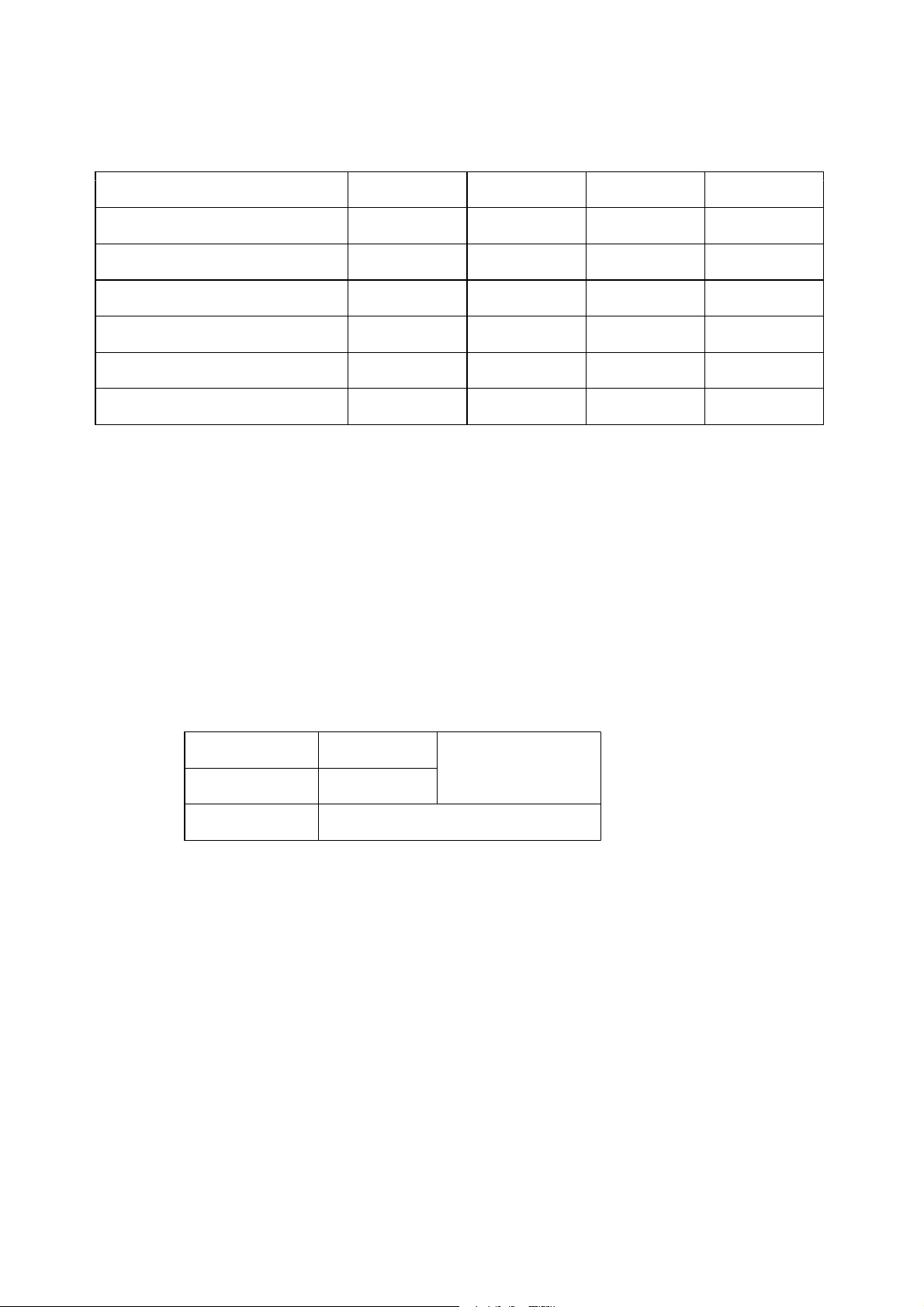
1. Application
This data sheet defines the specification for a (320×R.G.B)×240 dot, STN Transmissive color
dot matrix type Liquid Crystal Display with LED backlight. 『RoHS Compliance』
2. Construction and Outline
(320×R.G.B)×240 dots, COG type LCD with LED backlight.
Backlight system : Side‑edge type (LED).
Polarizer : Non‑Glare treatment.
Additional circuit : Bias voltage circuit, Randomizing circuit, DC‑DC converter
Polaizer
Backlight case
Color Filter
Glass
RGBRG B
Interface connector
This drawing is showing conception only.
GBRGB
R
Diffuser
PCB
Driver IC
LED
FPC
‑1‑
Page 5
3. Mechanical Specifications
ITEM SPECIFICATION UNIT
Outline dimensions 122.4(W) × 90.0(H) × 5.7(PCB and bosses are mm
not included)(D)
※Refer outline drawing in detail.
Effective viewing area 98.0 (W) × 74.0 (H) mm
Dot number (320×R.G.B) (W) × 240 (H) Dots
Dot size 0.08 (W) × 0.28 (H) mm
Dot pitch 0.10 (W) × 0.30 (H) mm
Display color *1 White *2 −
Base color *1 Black *2 −
Mass (90) g
*1 Due to the characteristics of the LC material, the color vary with environmental temperature.
*2 Negative‑type display
Display data "H" :R.G.B Dots ON : White
Display data "L" :R.G.B Dots OFF : Black
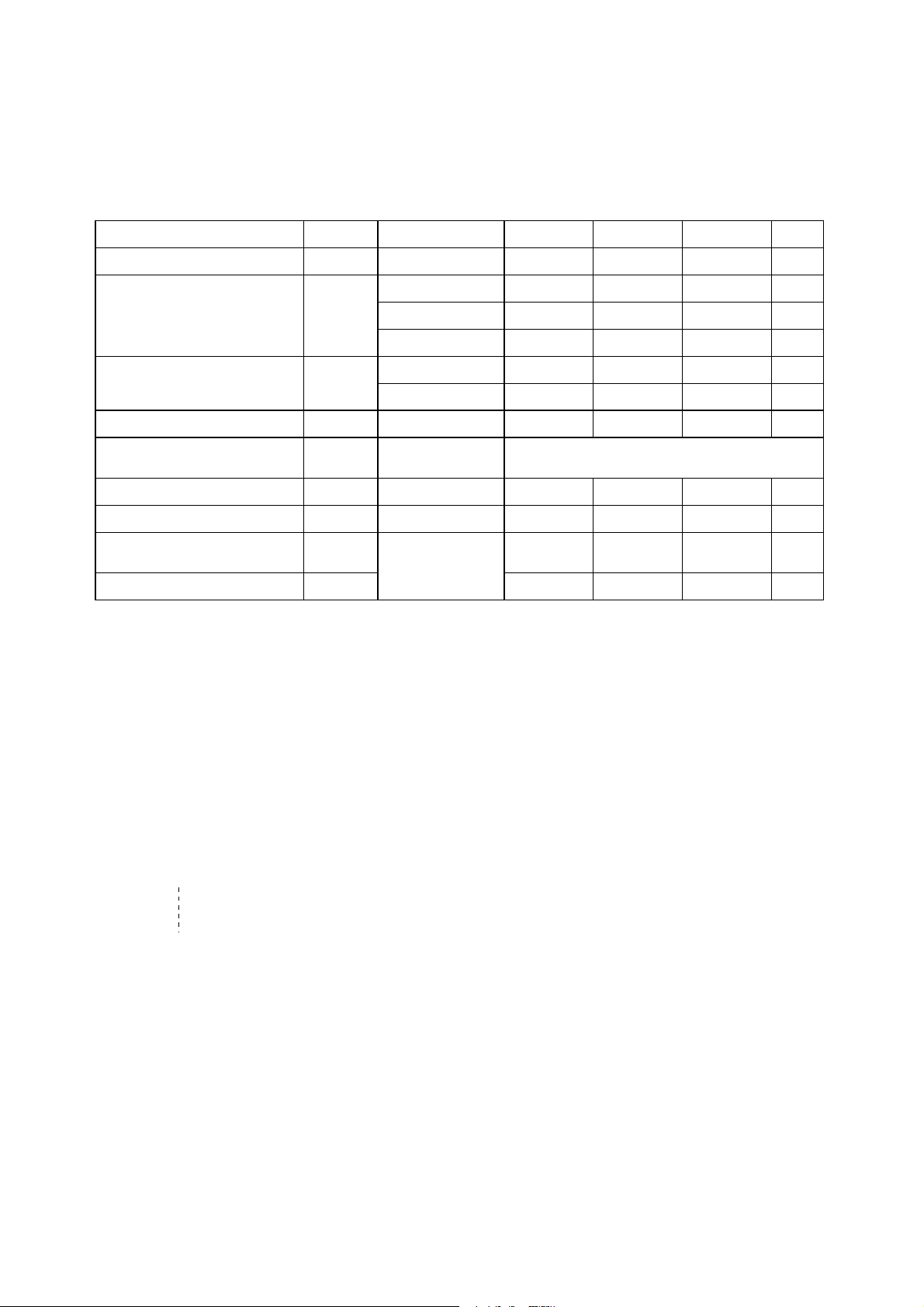
4. Absolute Maximum Ratings
4‑1. Electrical absolute maximum ratings
ITEM SYMBOL MIN. MAX. UNIT
Supply voltage for logic VDD 0 6.0 V
Supply voltage for LCD driving VCONT 0 VDD V
Input signal voltage for LCD *1 VinL 0 VDD V
FRM frequency f − 150 HzFRM
LED forward current (Backlight) IF − 12 mA
Supply voltage for backlight VinB 0 6.0 V
Backlight ON‑OFF BLEN 0 VinB V
Adjust brightness for backlight VBRT
*1 Input signal :CP, LOAD, FRM, DISP, D0〜D7
‑2‑
Page 6
4‑2. Environmental absolute maximum ratings
ITEM SYMBOL MIN MAX UNIT
Operating temperature *1 Top 0 50 ℃
Storage temperature *2 T ‑20 60 ℃STO
Operating humidity *3 Hop 10 *4 %RH
Storage humidity *3 H 10 *4 %RHSTO
Vibration − *5 *5 −
Shock − *6 *6 −
*1 LCD's display quality shall not be guaranteed at the temperature range of:
below 0℃ and upper 40℃.
*2 Temp. = (‑20℃) < (48h) , Temp = (60℃) < (168h)
Store LCD panel at normal temperature/humidity.
Keep it free from vibration and shock.
LCD panel that is kept at low or high temperature for a long time can be defective due to
the other conditions, even if the temperature satisfies standard.
(Please refers to 16. Precautions for use)
*3 Non‑condensation.
*4 Temp. ≦ 40℃, 85% RH Max.
Temp. > 40℃, Absolute Humidity shall be less than 85%RH at 40℃.
*5
Frequency 10〜55 Hz Converted to
acceleration value :
Vibration width 0.15 mm (0.3〜9 m/s )
2
Interval 10‑55‑10 Hz 1 minute
2 hours in each direction X/Y/Z (6 hours as total)
EIAJ ED‑2531
*6 Acceleration: 490m/s
2
Pulse width : 11 ms
3 times in each direction : ±X/±Y/±Z.
EIAJ ED‑2531
‑3‑
Page 7
5. Electrical Characteristics
5‑1. VDD=5.00V
VDD = 5.00V ± 0.25V , Temp. = 0〜50℃
ITEM SYMBOL CONDITION MIN. TYP. MAX. UNIT
Supply voltage for logic VDD − 4.75 5.00 5.25 V
LCD driving voltage *1 Vop= 0 ℃ 1.20 − − V
VCONT 25 ℃ 1.30 1.80 2.30 V
50 ℃ − − 2.40 V
Input voltage "H" level 0.8VDD − VDD V
(FRM,LOAD,CP,D0〜D7,DISP) VinL
Input current IinL Vin=VDD or VSS ‑100 − 100 μA
"L" level 0 − 0.2VDD V
Rush current for logic Irush When rush 3.0A(Peak) × 1ms
current happens
Clock frequency fcp − 2.02 2.16 5.88 MHz
Frame frequency *2 f − 70 75 150 HzFRM
Current consumption IDD *3 − (30) (45) mA
for logic
Power consumption Pdisp − (150) (225) mW
*1 Maximum contrast is obtained by adjusting the LCD driving voltage (Vop=Vcont) while at the
viewing angle of θ=φ=0°
*2 In consideration of display quality, it is recommended that frame frequency is set in the range
of 70‑80Hz. When you have to use higher frame and clock frequencies, confirm the LCD's performan
‑ce and quality prior to finalizing the frequency values:
Generally, as frame and clock frequencies become higher current consumption will get bigger and
display quality will be degraded.
*3 VDD=5.00V, VCONT = Vop, f = 75Hz, f = 2.16MHz, Temp. = 25℃
Display IDD max pattern:
1 2 3 4 5 6・・・・・・・・・・・・・・・・・・・・・・・・・・960(dot)
1
■■■■■■■■■■■■■■■■■■■■
2
□□□□□□□□□□□□□□□□□□□□
FRM CP
■■■■■■■■■■■■■■■■■■■■
□□□□□□□□□□□□□□□□□□□□
■■■■■■■■■■■■■■■■■■■■239
□□□□□□□□□□□□□□□□□□□□240
(dot)
‑4‑
Page 8
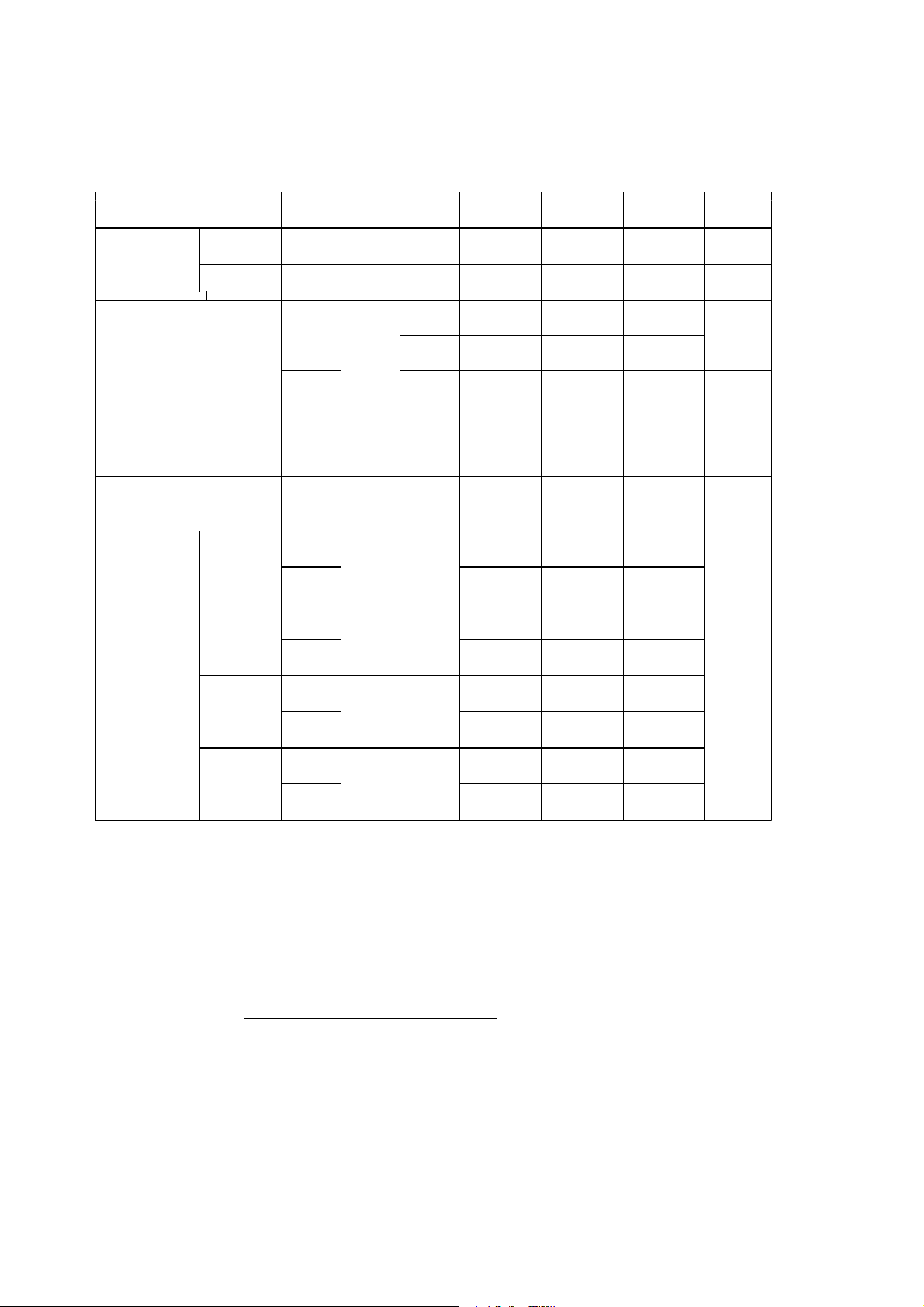
5‑2. VDD=3.30V
VDD = 3.30V ± 0.30V , Temp. = 0〜50℃
ITEM SYMBOL CONDITION MIN. TYP. MAX. UNIT
Supply voltage for logic VDD − 3.00 3.30 3.60 V
LCD driving voltage *1 Vop= 0 ℃ 1.20 − − V
VCONT 25 ℃ 1.30 1.80 2.30 V
50 ℃ − − 2.40 V
Input voltage "H" level 0.8VDD − VDD V
(FRM,LOAD,CP,D0〜D7,DISP) Vin
"L" level 0 − 0.2VDD V
Input current Iin Vin=VDD or VSS ‑100 − 100 μA
Rush current for logic Irush When rush 3.0A(Peak) × 1ms
current happens
Clock frequency fcp − 2.02 2.16 5.88 MHz
Frame frequency *2 f − 70 75 150 HzFRM
Current consumption IDD *3 − (45) (68) mA
for logic
Power consumption Pdisp − (150) (225) mW
*1 Maximum contrast is obtained by adjusting the LCD driving voltage (Vop=Vcont) while at the
viewing angle of θ=φ=0°
*2 In consideration of display quality, it is recommended that frame frequency is set in the range
of 70‑80Hz. When you have to use higher frame and clock frequencies, confirm the LCD's performan
‑ce and quality prior to finalizing the frequency values:
Generally, as frame and clock frequencies become higher current consumption will get bigger and
display quality will be degraded.
*3 VDD=3.30V, VCONT = Vop, f = 75Hz, f = 2.16MHz, Temp. = 25℃
Display IDD max pattern:
1 2 3 4 5 6・・・・・・・・・・・・・・・・・・・・・・・・・・960(dot)
1
■■■■■■■■■■■■■■■■■■■■
2
□□□□□□□□□□□□□□□□□□□□
FRM CP
■■■■■■■■■■■■■■■■■■■■
□□□□□□□□□□□□□□□□□□□□
239
■■■■■■■■■■■■■■■■■■■■
□□□□□□□□□□□□□□□□□□□□240
(dot)
‑5‑
Page 9
6.Optical Characteristics
ITEM SYMBOL CONDITION MIN. TYP. MAX. UNIT
Response Rise Tr θ=φ=0° − (190) (290) ms
time
Down Td θ=φ=0° − (180) (280) ms
Upper − (20) −
θ deg.
Lower − (30) −
Viewing angle range CR≧2
Left − (50) −
φ deg.
Right − (50) −
Contrast ratio CR θ=φ=0° (15) (30) − −
Temp. = 25℃
Brightness L − (70) (120) − cd/m
2
(IF=10mA/1 LED line)
Chromaticity x (0.44) (0.49) (0.54)
coordinates Red θ=φ=0°
y (0.30) (0.35) (0.40)
x (0.24) (0.29) (0.34)
Green θ=φ=0°
y (0.43) (0.48) (0.53)
−
x (0.10) (0.15) (0.20)
Blue θ=φ=0°
y (0.07) (0.12) (0.17)
x (0.22) (0.27) (0.32)
White θ=φ=0°
y (0.24) (0.29) (0.34)
Optimum contrast is obtained by adjusting the LCD driving voltage (Vop=Vcont) while at the
viewing angle of θ=φ=0°
6‑1. Contrast ratio is defined as follows:
Brightness at all pixels "White"
CR =
Brightness at all pixels "Black"
‑6‑
Page 10
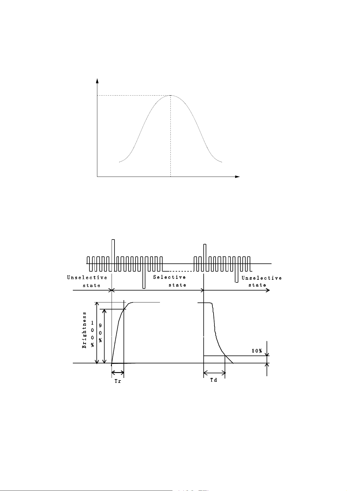
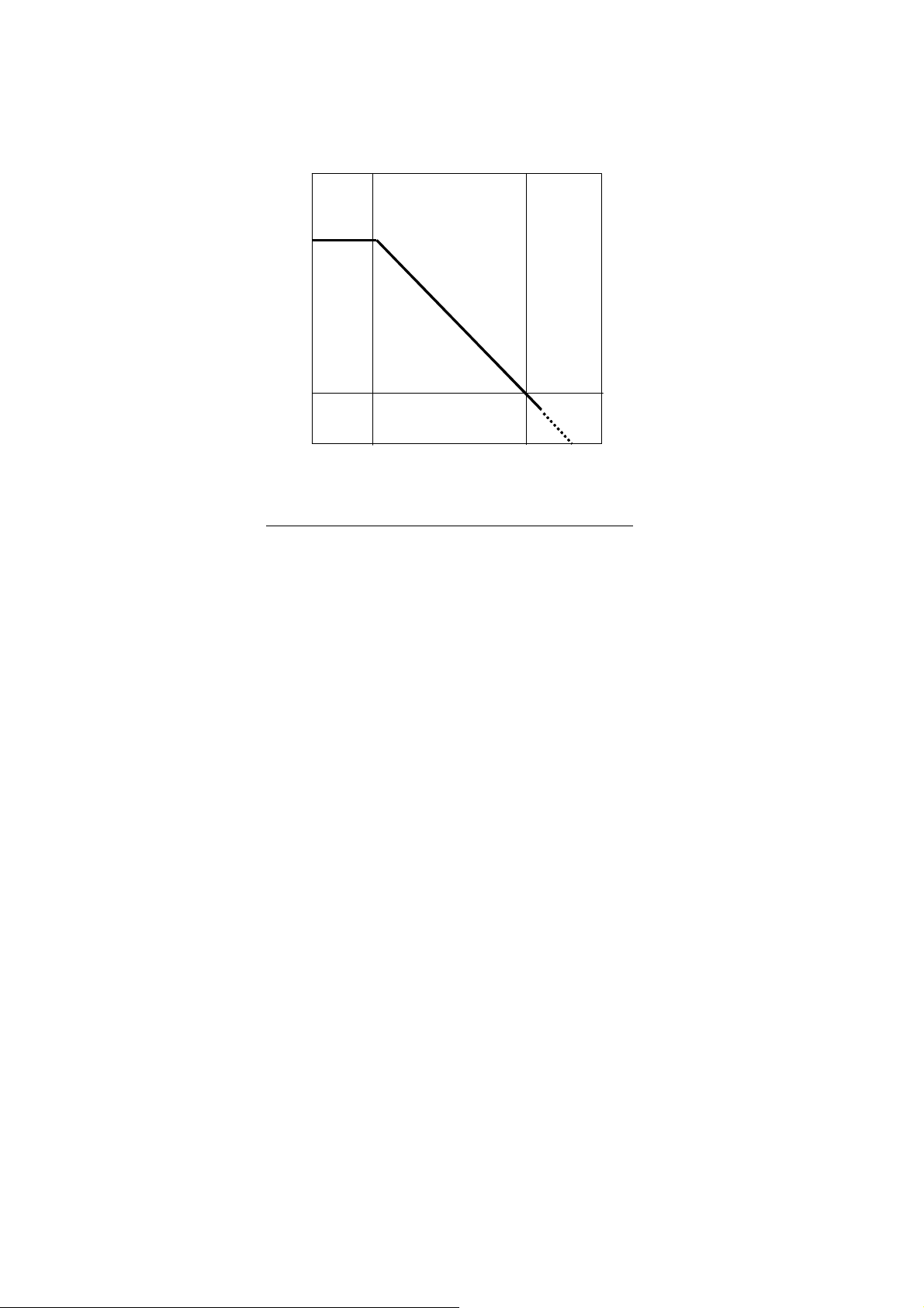
6‑2. Definition of Vop
C
o
n
t
x
a
m
R
C
r
a
s
t
VCONT (V)
Vop
6‑3. Definition of response time
‑7‑
Page 11

6‑4. Definition of viewing angle
Y
+
X
‑
(θdi
6‑5. Measuring points
φ=0°
θ
+
‑
θ
‑
rection )
=
0
θ
°
Y
+
+
φ
φ
+
X
‑Y
i
o
)
d
i
r
n
t
e
c
φ
‑
X
+
Y
X
‑
(
80×3 160×3 240×3 (dot)
14
60 ○ ○
3
120 ○
25
180 ○ ○
(dot)
1) Rating is defined as the average brightness inside the viewing area.
2) 30 minutes after LED is turned on. (Ambient Temp.=25℃)
‑8‑
Page 12
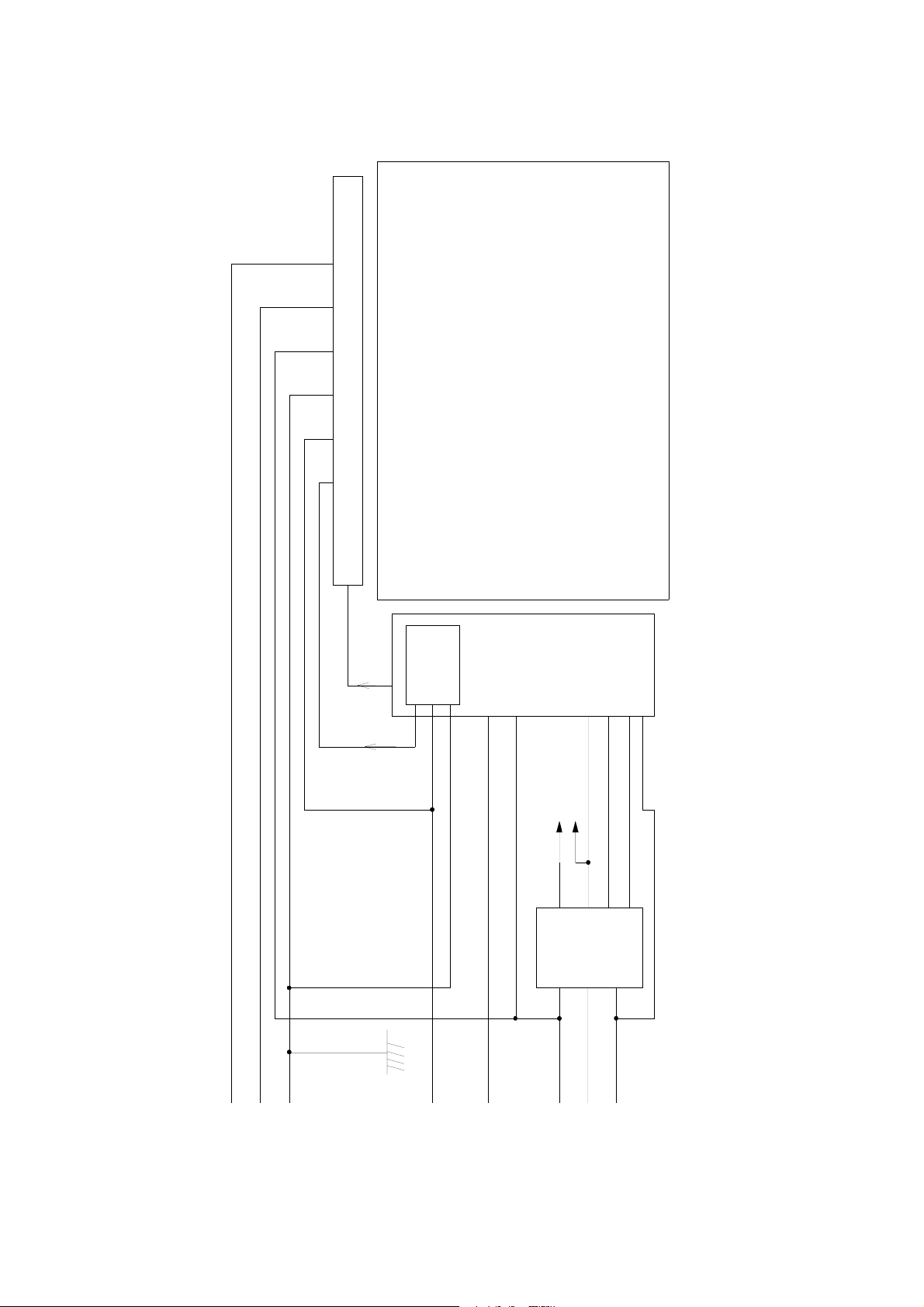
7. Circuit Block Diagram
y
t
u
d
0
C
I
r
e
v
i
r
D
G
E
S
4
2
/
1
(320 × R.G.B) × 240 LCD
DISP
DF
g
n
i
t
z
i
i
u
m
c
o
r
d
n
a
R
COM
i
c
Driver IC
To SEG IC
To SEG IC
V0
VM
DC/DC
VH
converter
VL
0〜D7
CP
VSS
VSS=V1
LOAD
‑9‑
FRM
VDD
T
CON
DISP
Page 13
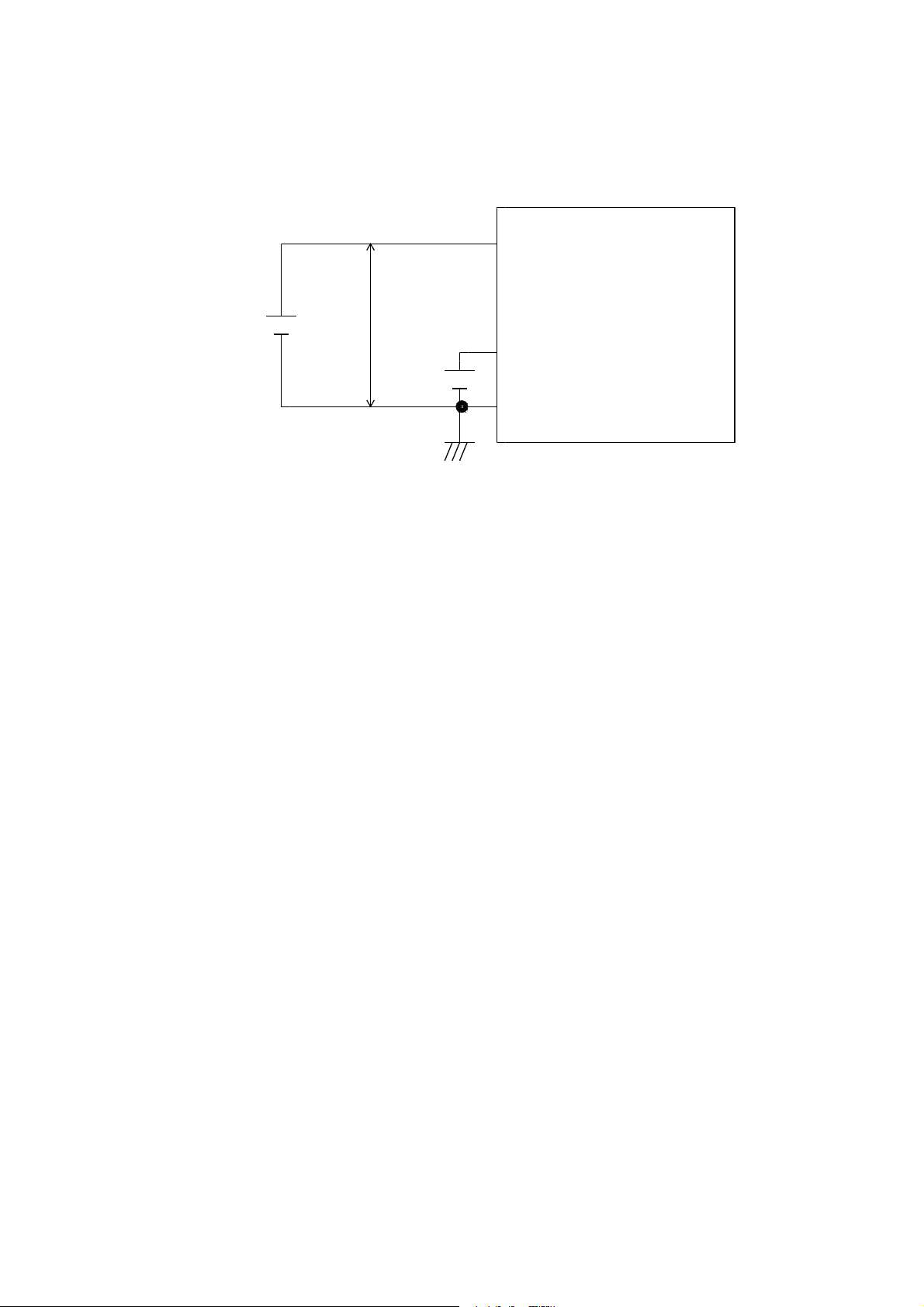
7‑1. Power supply
(+1.2V〜2.4V)
VCONT
Vop
KCG047QVL
VDD
3.3V or
5.0V
VSS
‑10‑
Page 14

8. Interface signals
8‑1. LCD
PIN NO. SYMBOL DESCRIPTION LEVEL
1 FRM Synchronous signal for driving scanning line H
2 LOAD Data signal latch clock H → L
3 CP Data signal shift clock H → L
4 DISP Display control signal H(ON),L(OFF)
5 VDD Power supply for logic ―
6 VSS GND ―
7 VCONT LCD adjust voltage ―
8D7
9D6
10 D5
11 D4 Display data H(ON),L(OFF)
12 D3
13 D2
14 D1
15 D0
16 VDD Supply voltage for logic −
17 VDD
18 VSS GND −
19 VSS
20 VSS
LCD side connector : 08‑6210‑020‑340‑800+ (ELCO)
Recommended matching connector : 0.5mm pitch FFC or FPC
8‑2. Backlight
PIN No. SYMBOL DESCRIPTION
1 VinB
2 VinB Supply voltage
3 VinB
4 VinB
5 BLEN Backlight ON‑OFF (H : ON , L : OFF)
6 VBRT Brightness adjust voltage
7GND
8 GND GND
9GND
10 GND
Backlight side connector : 08‑6210‑010‑340‑800+ (ELCO)
Recommended matching connector : 0.5mm pitch FFC or FPC
‑11‑
Page 15

9.Interface Timing Chart
LOAD
CP
D7 G318 R1 B3 G318 R1
D6 B318 G1 R4 B318 G1
D5 R319 B1 G4 R319 B1
D4 G319 R2 B4 G319 R2
D3 B319 G2 R5 B319 G2
D2 R320 B2 G5 R320 B2
D1 G320 R3 B5 G320 R3
D0 B320 G3 R6 B320 G3
FRM
CP × (320×R.G.B) / 8 pulse
LOAD
×1 ×2 ×240 ×1
D0〜D7
FRM
* The cycle of load signal should be stable and continuously applied without interruption.
‑12‑
rating.* The above‑mentioned timing chart shows a reference to set up a LCD module, not an electrical
Page 16

10.Data and Screen
CHIP AREA
Y1 Y2 Y3 ・・・ Y320
CX1
H D7D6D5D4D3D2D1D0D7 D2D1D0
I R1 G1 B1 R2 G2 B2 R3 G3 B3 R320 G320 B320
P
A
R
E
A
X240
‑13‑
Page 17

11. Input Timing Characteristics
trCP tfCP
tWCLH tWCLL tCCL
CP
tDS tDH
DATA
CP
LOAD
FRM
tCDLD
last 1st 1st
tLDCR
tWLPH
tLCL
tWLPL
tr tf
tFS tFH
‑14‑
Page 18

11‑1. Switching characteristics (VDD = 5.00V)
Input Characteristics ; VDD = 5.00V ± 0.25V, Temp. = 0〜50 ℃
ITEM SYMBOL MIN. MAX. UNIT
CP Cycle *1 tCCL 100 − ns
CP "H" Pulse Width tWCLH 30 − ns
CP "L" Pulse Width tWCLL 30 − ns
CP Rise Up Time trCP − 15 ns
CP Fall Down Time tfCP − 15 ns
Data Set Up Time tDS 25 − ns
Data Hold Time tDH 25 − ns
LOAD "H" Pulse Width tWLPH 40 − ns
LOAD "L" Pulse Width tWLPL 400 − ns
LOAD Cycle *2 tLCL 500 − ns
CP Down→LOAD Down Delay Time tCDLD 60 − ns
LOAD Down→CP Rise Delay Time tLDCR 60 − ns
Input Signal Rise Up Time tr − 20 ns
Input Signal Fall Down Time tf − 20 ns
FRM Data Set Up Time tFS 120 − ns
FRM Data Hold Time tFH 30 − ns
*1 CP Cycle is adjust so that FRM signal is 75Hz.
*2 Load cycle is const.
‑15‑
Page 19
11‑2. Swutching characteristics (VDD = 3.30V)
Input Characteristics ; VDD = 3.30V ± 0.30V, Temp. = 0〜50 ℃
ITEM SYMBOL MIN. MAX. UNIT
CP Cycle *1 tCCL 100 − ns
CP "H" Pulse Width tWCLH 40 − ns
CP "L" Pulse Width tWCLL 40 − ns
CP Rise Up Time trCP − 20 ns
CP Fall Down Time tfCP − 20 ns
Data Set Up Time tDS 35 − ns
Data Hold Time tDH 35 − ns
LOAD "H" Pulse Width tWLPH 50 − ns
LOAD "L" Pulse Width tWLPL 400 − ns
LOAD Cycle *2 tLCL 500 − ns
CP Down→LOAD Down Delay Time tCDLD 60 − ns
LOAD Down→CP Rise Delay Time tLDCR 80 − ns
Input Signal Rise Up Time tr − 20 ns
Input Signal Fall Down Time tf − 20 ns
FRM Data Set Up Time tFS 120 − ns
FRM Data Hold Time tFH 30 − ns
*1 CP Cycle is adjust so that FRM signal is 75Hz.
*2 Load cycle is const.
‑16‑
Page 20

12. Supply Voltage Sequence Condition
V
V
Always follow the power supply ON / OFF sequence as specified below.
Unless you follow the power supply ON / OFF sequences, driving circuit in the LCD may
irreparably break and / or DC voltage may be supplied to the LCD.
DC voltage induces irreversible electrochemical reactions on the screen and reduce LCD life.
DD
0ms MIN
0ms MIN
Input signal
CONT
0ms MIN 0ms MIN
DISP
* Input signal : CP, LOAD, FRM,D0〜D7
Each signal (CP,LOAD,FRM) is constant.
* The above sequence should be designed as to keep each normal figure on condition that
liquid crystal module is loaded on your system.
* Control the supply voltage sequence not to float all signal line when the LCD panel is
driving.
‑17‑
Page 21

13. LED Backlight Characteristics
13‑1. LED Backlight Characteristics
Temp. = 25℃
ITEM Symbol MIN TYP. MAX UNIT NOTE
Supply voltage VinB 3.0 − 5.5 V 0〜50℃
ON‑OFF (H) 0.8VinB − VinB −
BLEN V
ON‑OFF (L) 0.0 − 0.2VinB −
9.0 10.0 11.0 VBRT=0〜0.8V
Output current *1 IF mA
− (2.0) − VBRT=2.8V
− (290) (350) VinB=3.3V,IF=10mA *1
Supply current IinB mA
− (180) (220) VinB=5.0V,IF=10mA *1
Operating Life *2 T (T.B.D.) (50,000) *3 − hour IF=10mA *1
*1 Between AN1‑CA1 and between AN2‑CA2 each. (Please refer to below drawing.)
AN1
AN1
(Anode)
(Anode)
AN2
AN2
(Anode)
(Anode)
*2 When surface brightness decreases 50% of initial brightness .
*3 Life time is estimated data.
*4 When you start‑up, please charge in sequence of VinB‑>BLEN, or VBRT.
When you shut‑down, please stop in sequence of BLEN and/or VBRT‑>VinB.
*5 Please do not connect the other than our backlight to this output connector on the PCB.
CN1
CN1
(Cathode)
(Cathode)
CN2
CN2
(Cathode)
(Cathode)
‑18‑
Page 22

*6 In case VDD and VIN are supplied by a single power source, VDD & VIN, and VSS & GND are
connected directly and separately from the output on the power source. If the common wire are
used for VDD & VIN, and for VSS & GND, and are split near the PCB, and connect to each LCD
driving circuit and backlight driving circuit, a flicker might be occurred due to a ripple
between the both circuit.
Right
VINOutput terminal
GND
KCG047 PCBPower supply
e)(Customer sid
VDD
VSS
Wrong
VINOutput terminal
GND
KCG047 PCBPower supply
e)(Customer sid
VDD
VSS
‑19‑
Page 23
13‑2. VBRT‑IF characteristics
IF(mA)
VBRT‑IF characteristics (reference) Ta=25℃
10
2.0
0.8 2.8
VBRT(V)
‑20‑
Page 24

14.Lot Number Identification
The lot number shall be indicated on the back of the backlight case of each LCD.
KCG047QVLAB−A21 − □ □−□ □ −□
Version Number.
DATE
MONTH
YEAR
YEAR 2005 2006 2007 2008 2009 2010
CODE 5 6 7 8 9 0
MONTH JAN. FEB. MAR. APR. MAY JUN.
CODE 1 2 3 4 5 6
MONTH JUL. AUG. SEP. OCT. NOV. DEC.
CODE 7 8 9 X Y Z
15.Warranty
15‑1. Incoming inspection
Please inspect the LCD within one month after your receipt.
15‑2. Production Warranty
Kyocera warrants its LCDs for a period of 12 months after receipt by the purchaser, and within
the limits specified. Kyocera shall, by mutual agreement, replace or rework defective LCDs
that are shown to be Kyocera's responsibility.
‑21‑
Page 25

16.Precautions for use
16‑1. Installation of the LCD
1. Please ground of an LCD module, in order to stabilize brightness and display quality.
2. The LCD shall be installed so that there is no pressure on the LSI chips.
3. The LCD shall be installed flat, without twisting or bending.
4. The display window size should be the same as the effective viewing area.
5. In case you use outside frame of effective viewing area as outward appearance of your product,
unevenness of its outward appearance is out of guarantee.
6. This Kyocera LCD module has been specifically designed for use in general electronic devices,
but not for use in a special environment such as usage in an active gas.
Hence, when the LCD is supposed to be used in a special environment, evaluate the LCD
thoroughly beforehand and do not expose the LCD to chemicals such as an active gas.
16‑2. Static Electricity
1. Since CMOS ICs are mounted directly onto the LCD glass, protection from static electricity is
required. Operation should wear ground straps.
16‑3. LCD Operation
1. The LCD shall be operated within the limits specified. Operation at values outside of these
limits may shorten life, and/or harm display images.
2. Adjust "LCD driving voltage" to obtain optimum viewing angle and contrast.
3. Operation of the LCD at temperature below the limit specified may cause image degradation
and/or bubbles.
It may also change the characteristics of the liquid crystal.
This phenomenon may not recover. The LCD shall be operated within the temperature limits
specified.
16‑4. Storage
1. The LCD shall be stored within the temperature and humidity limits specified.
Store in a dark area, and protected the LCD from direct sunlight or fluorescent light.
2. Always store the LCD so that it is free from external pressure onto it.
16‑5. Screen Surface
1. DO NOT store in a high humidity environment for extended periods.
Image degradation, bubbles, and/or peeling off of polarizer may result.
2. The front polarizer is easily scratched or damaged.
Prevent touching it with any hard material, and from being pushed or rubbed.
3. The LCD screen may be cleaned with a soft cloth or cotton pad.
Methanol, or Isopropyl Alcohol may be used, but insure that all solvent residue is removed.
4. Water may cause damage or discoloration of the polarizer.
Clean any condensation or moisture from any source immediately.
5. Always keep the LCD free from condensation during testing.
Condensation may permanently spot or stain the polarizers.
6.Please do not use solid‑base image pattern for long hours because a temporary afterimage may
appear. We recommend to use screen saver etc. in cases where a solid‑base image pattern must
be used.
7.Liquid crystal may leak when the module is broken. Be careful not to let the fluid
go into your eyes and mouth. In the case the fluid touches your body, rinse it off
right away with water and soap.
‑22‑
Page 26
17.Reliability Data / Environmental Test
TEST TEST TEST RESULT
ITEM CONDITION TIME
High Temp. (70℃) (240 h) Display Quality : No defect
Atmosphere Display Function : No defect
Current Consumption : No defect
Low Temp. Bubble : None
Solid Crystallization of
Low Temp. (‑20℃) (240 h) Liquid Crystal : None
Atmosphere Display Quality : No defect
Display Function : No defect
Current Consumption : No defect
Display Quality : No defect
High Temp. (40℃) (240 h) Display Function : No defect
Humidity (90%RH) Peel‑off of Organic
Atmosphere Sealing : None
Current Consumption : No defect
Display Quality : No defect
Temp. Cycle (‑20℃ 0.5 h) (10 cycles) Display Function : No defect
(R.T. 0.5 h) Peel‑off of Organic
(70℃ 0.5 h) Sealing : None
Bubble on Cell : None
High Temp. (50℃) (240 h) Display Quality : No defect
Operation (Vop) Display Function : No defect
Current Consumption : No defect
* Each test item uses a test LCD only once. The tested LCD is not used in any other tests.
* The LCD is tested in circumstances in which there is no condensation.
* The tested LCD is inspected after 24 hours of storage at room temperature and room humidity
after each test is finished.
* The reliability test is not an out‑going inspection.
* The results of the reliability test are for your reference purpose only.
The reliability test is conducted only to examine the LCD's capability.
‑23‑
Page 27

Page 28
Page 29
Revision Record
Designed by: Engineering Dept. Confirmed by: QA Dept.
Date
Prepared Checked Approved Checked Approved
Rev. No. Date Page Descriptions
Page 30
Visuals specification
1)Note
Item Note
General 1.When d efects specified in this Inspection Standards are
inspected, o perating voltage (Vop) shall be set at the
level where optimized c ontrast is available.
Display qual ity is applied up to effective viewing area.
(Bi-Level INSPEC TION)
2.This inspect ion standard about the image quality shall be
applied to any defect within the effective viewing area
and shall not be applicable to outside of the ar ea.
3.Should any defects whic h are not specified in this
standard hap pen, additional standard shall be de termined
by mutual agreement bet ween customer and Kyocera .
4.Inspection c onditions
Luminance : 500 Lux minimum .
Inspection d istance : 300 mm (from the sample)
Temperature : 25 ± 5 ℃
Direction : right above
Definition of Inspection Pin hole, Bright spot The color of a sma ll area is
item Black spot, Scratch different fro m the remainder.
Foreign partic le The phenomenon does not chang e
with voltage.
Contrast varia tion The color of a small are a is
different fro m the remainder.
The phenomeno n changes with
voltage.
Polarizer ( Scratch, Scratch, Bubble and Dent in the
Bubble, Dent ) polarizer which can be observed
in on / off state.
-1-
Page 31
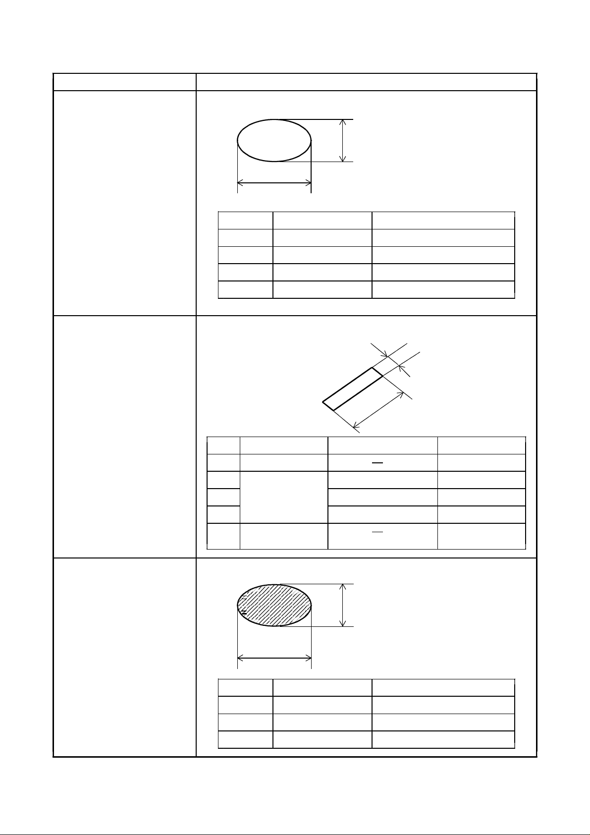
2)Standard
Inspection item Judgement sta ndard
Pinhole, Bright spot
Black spot,
Foreign particl e
Scratch,Foreign particle
b
a
d=(a+b)/2
Category Size (mm) Acce ptable number
Ad≦ 0.2 neglected
B 0.2 < d ≦ 0.3 5
C 0.3 < d ≦ 0.5 3
D 0.5 < d0
W
Contrast variat ion
L
Width (mm) Length (mm) Acceptable No.
AW≦ 0.03 neglected
BL≦ 2.0 neglected
C 0.03< W ≦ 0.1 2.0 < L ≦ 4.0 3
D 4.0 < L0
E 0.1 < W According to
' Circular '
b
a
d=(a+b)/2
Category Size (mm) Acceptable number
Ad≦ 0.5 neglected
B 0.5 < d ≦ 0.7 3
C 0.7 < d0
-2-
Page 32

Inspection item Judgement sta ndard
Polarizer ( Scratch, (1) Scratch W
Bubble, Dent )
L
Width (mm) Length (mm) Acceptable No.
AW≦ 0.1 neg lected
BL≦ 5.0 neglected
0.1 < W ≦ 0.3
C 5.0 < L0
D 0.3 < W0
(2)Bubble ( dent )
b
a
d=(a+b)/2
Category Size (mm) Acce ptable number
Ad≦ 0.2 neglected
B 0.2 < d ≦ 0.3 5
C 0.3 < d ≦ 0.5 3
D 0.5 < d0
-3-
 Loading...