

Page 1
If it’s embedded, it’s Kontron
KTQ67/Flex-Medical Users Guide
KTD-N0849-D
Page 2

KTQ67/Flex -Medical Users Guide
KTD-N0849-D Page 2
Revision
Date
By
Comment
Correction of MIC2 and Line2 location. EXT_BAT max. 3.47V.
C
Jan. 8th 2014
MLA
Added BIOS features: Force Boot Setup and PC Speaker/Beep.
B
Dec. 13th 2013
MLA
Revision merged KTD-N00829-E KTQ67 Users Guide.
A
Aug. 22nd 2013
MLA
First release
0
Aug. 26th 2011
MLA
Preliminary version
Document details
Document revis ion history.
D Jan. 19th 2015 MLA
Chapter 7.22 Riser card note corrected.
Copyright Notice:
Copyright 2011, KONTRON Technology A/S, ALL RIGHTS RESERVED.
No part of this document may be reproduced or transmitted in any form or by any means, electronically
or mechanically, for any purpose, without the express written permission of KONTRON Technology A/S.
Trademark Acknow ledgemen t:
Brand and product names are trademarks or registered trademarks of their respective owners.
Disclaimer:
KONTRON Technology A/S reserves the right to make changes, without notice, to any product,
including circuits and/or software described or contained in this manual in order to improve design
and/or performance.
Specifications listed in this manual are subject to change without notice. KONTRON Technology
assumes no respons ibility or liabil ity for the use of the described produc t(s), conve ys no license or titl e
under any patent, cop yright, or mask work rights to these pro ducts, and makes no representat ions or
warranties that these products are free f rom patent, copyright, or mask work right infringement, u nless
otherwise specified. Applications that are described in this manual are for illustration purposes only.
KONTRON Technolog y A/S makes no r epresentation or warranty that such a pplication will be suitable
for the specified use without further testing or modification.
Life Support Polic y
KONTRON Technology’s PRODUCTS ARE NOT FOR USE AS CRITICAL COMPONENTS IN LIFE
SUPPORT DE VICES OR S YSTEMS WITHOUT EXPR ESS W R ITTEN APPRO V AL OF T HE G ENER AL
MANAGER OF KONTRON Technology A/S.
As used herein:
Life support devices or s ystems are devices or systems which, (a) are intended f or surgical im plant int o
body, or (b) support or s ustain life an d whos e fail ure to per form , when prop erl y used i n accor dance w ith
instructions for use prov ided i n the labelling, can be reasonab l y expected to r esult in sig nificant injury to
the user.
A critical component is an y component of a life suppo rt device or system whose failure to perform can
be reasonably expected to c ause the f ailure of the life s upport de vice or s ystem , or to affect its safet y or
effectiveness.
Page 3

KTQ67/Flex -Medical Users Guide
KTD-N0849-D Page 3
Document details
KONTRON Technology Technical Support & Services
If you have questio ns about installing or using your KONT RON Technology Pro duct, check this User ’s
Manual first – you will find answers to mos t questions her e. T o obtain supp ort, pl ease contac t your local
Distributor or Field Application Engineer (FAE).
Before Contacting Support: Please be prepared to provide as much information as possible:
• CPU Board
1. Type.
2. Part Number (find PN on label)
3. Serial Number if available (find SN on label)
• Configuration
1. CPU Type, Clock speed
2. DRAM Type and Size.
3. BIOS Revision (Find the Version Info in the BIOS Setup).
4. BIOS Settings different than Default Settings (Refer to the BIOS Setup Section).
• System
1. O/S Make and Version.
2. Driver Version numbers (Graphics, Network, and Audio).
3. Attached Hardware: Harddisks, CD-rom, LCD Panels etc.
Warranty
KONTRON Technology warrants its products to be free from defects in material and workmanship
during the warrant y period. If a pr oduct proves to be defective in material or workmanship during the
warranty period, KONTRON Technology will, at its sole option, repair or replace the product with a
similar product.
Replacement Product or parts may include remanufactured or refurbished parts or components.
The warranty does not cover:
1. Damage, deterioration or malfunction resulting from:
A. Accident, misuse, neg lect, fire, water, lightning, or oth er acts of nature, una uthorized produc t
modification, or failure to follow instructions supplied with the product.
B. Repair or attempted repair by anyone not authorized by KONTRON Technology.
C. Causes external to the product, such as electric power fluctuations or failure.
D. Normal wear and tear.
E. Any other causes which does not relate to a product defect.
2. Removal, installation, and set -up service charges.
Exclusion of damages:
KONTRON TECHNOLOGY LIABILIT Y IS LIMITED TO THE COST OF REPAIR OR REPLACEMENT
OF THE PRODUCT. KONTRON TECHNOLOGY SHALL NOT BE LIABLE FOR:
1. DAMAGE TO OTHER PROPERTY CAUSED BY ANY DEFECTS IN THE PRODUCT,
DAMAGES BASED UPON INCONVE NIENCE, LOS S OF USE OF TH E PRODUCT, LOSS OF
TIME, LOSS OF PROFITS, LOSS OF BUSINESS OPPORTUNITY, LOSS OF GOODWILL,
INTERFERENCE WITH BUSINESS RELATIONSHIPS, OR OTHER COMMERCIAL LOSS,
EVEN IF ADVISED OF THEIR POSSIBILITY OF SUCH DAMAGES.
2. ANY OTHER DAMAGES, WHETHER INCIDENTAL, CONSEQUENTIAL OR OTHERWISE.
3. ANY CLAIM AGAINST THE CUSTOMER BY ANY OTHER PARTY.
Page 4

KTQ67/Flex -Medical Users Guide
KTD-N0849-D Page 4
Contents
Introduction ............................................................................................. 7
1 Installation procedure ........................................................................ 8
1.1 Installing the board .......................................................................................................................... 8
1.2 Requirement according to IEC60950 ................................................................................................... 9
2 System Specification ........................................................................ 10
2.1 Component main data ..................................................................................................................... 10
2.2 System overview ............................................................................................................................. 14
2.3 Processor Support Table .................................................................................................................. 16
2.4 System Memory support ................................................................................................................... 19
2.5 KTQ67 Graphics Subsystem ............................................................................................................... 20
2.5.1 Intel® HD Graphics 3000 (example) ................................................................................................ 20
2.6 Power Consumption ........................................................................................................................ 21
3 Connector Locations ......................................................................... 24
3.1 KTQ67/Flex-Medical – frontside ........................................................................................................ 24
4 Connector Definitions ....................................................................... 26
5 IO-Area Connectors ........................................................................... 27
5.1 Display connectors (IO Area) ............................................................................................................ 27
5.1.1 DVI (lower) connector – DVI-I ......................................................................................................... 27
5.1.2 DVI-D (upper) connector – DVI-D ..................................................................................................... 28
5.2 Ethernet Connectors (IO Area).......................................................................................................... 29
5.3 USB Connectors (IO Area) ................................................................................................................ 30
5.3.1 USB Connector 0/1/2/3 (USB0/1/2/3) ............................................................................................ 30
5.4 COM1 and COM2 Connectors (IO Area) ............................................................................................... 31
6 Internal Connectors .......................................................................... 32
6.1 Power Connector (ATX/BTXPWR) ....................................................................................................... 32
6.2 Fan Connectors (FAN_CPU) (J28) and (FAN_SYS) (J29) ....................................................................... 33
6.3 PS/2 Keyboard and Mouse connector (KBDMSE) (J15)......................................................................... 34
Page 5

KTQ67/Flex -Medical Users Guide
KTD-N0849-D Page 5
6.4
Display connectors (Internal) ........................................................................................................... 35
6.4.1 LVDS Flat Panel Connector (LVDS) (J39) (optionally) ......................................................................... 35
6.5 SATA (Serial ATA) Disk interface (J22 – J27) ...................................................................................... 36
6.6 USB Connectors (USB) ..................................................................................................................... 37
6.6.1 USB Connector 6/7 ........................................................................................................................ 37
6.6.2 USB Connector 8/9 (USB8/9) (J18) ................................................................................................. 37
6.6.3 USB Connector 10/11 (USB10/11) (J17) .......................................................................................... 38
6.6.4 USB Connector 12/13 (USB12/13) (J16) .......................................................................................... 38
6.7 Serial COM3 – COM4 Ports (J20, J21) ................................................................................................. 39
6.8 Audio Connector ............................................................................................................................. 40
6.8.1 Line2 and Mic2 .............................................................................................................................. 40
6.8.1 Audio Header Connector (AUDIO_HEAD) (J47) ................................................................................. 40
6.9 Power Button Connector (PWRBTN) (J48) .......................................................................................... 41
6.10 Front Panel Connector (FRONTPNL) (J36) .......................................................................................... 42
6.11 Feature Connector (FEATURE) (J30) .................................................................................................. 43
6.12 ”Load Default BIOS Settings” Jumper (J11) ....................................................................................... 45
6.13 ClrRTC (J12) ................................................................................................................................... 45
6.14 SPI Recover Jumper (J41) ................................................................................................................ 46
6.15 SPI Connector (SPI) (J40) ................................................................................................................ 47
6.16 XDP-CPU (Debug Port for CPU) (J14) ................................................................................................. 48
6.17 XDP-PCH (Debug Port for Chipset) (J13) ............................................................................................ 49
7 Slot Connectors (PCIe, PCI)............................................................... 50
7.1 PCIe Connectors.............................................................................................................................. 50
7.1.1 PCI-Express x16 Connector (PCIe x16).............................................................................................. 50
7.1.3 PCI-Express x4 Connector (PCIe x4) (J33) ........................................................................................ 52
7.2 PCI Slot Connectors ........................................................................................................................ 53
7.2.1 Signal Description – PCI Slot Connector ........................................................................................... 54
7.2.2 KTQ67 PCI IRQ & INT routing ........................................................................................................... 55
8 On-board - & mating connector types ................................................. 56
9 System Resources ............................................................................. 57
9.1 Memory Map ................................................................................................................................... 57
9.2 PCI Devices .................................................................................................................................... 58
9.3 Interrupt Usage .............................................................................................................................. 59
9.4 IO Map ........................................................................................................................................... 60
Page 6

KTQ67/Flex -Medical Users Guide
KTD-N0849-D Page 6
10 BIOS ................................................................................................ 61
10.1 Main .............................................................................................................................................. 61
10.2 Advanced ....................................................................................................................................... 62
10.2.1 Advanced - PCI Subsystem Settings ................................................................................................ 63
10.2.2 Advanced - APCI Settings ............................................................................................................. 68
10.2.3 Advanced - Trusted Computing ...................................................................................................... 69
10.2.4 Advanced - CPU Configuration ....................................................................................................... 70
10.2.5 Advanced - SATA Configuration ...................................................................................................... 72
10.2.6 Advanced - Intel ® Rapid Start Technology ..................................................................................... 76
10.2.7 Advanced - Intel TXT (LT) Configuration .......................................................................................... 77
10.2.8 Advanced - Intel ® Anti-Theft Technology Configuration .................................................................. 78
10.2.9 Advanced - AMT Configuration ....................................................................................................... 79
10.2.10 Advanced - Acoustic Management Configuration ............................................................................. 81
10.2.11 Advanced - USB Configuration ....................................................................................................... 82
10.2.12 Advanced - SMART Settings ........................................................................................................... 83
10.2.13 Advanced - Super IO Configuration................................................................................................. 84
10.2.14 Advanced - Voltage Monitor .......................................................................................................... 89
10.2.15 Advanced - Hardware Health Configuration ..................................................................................... 90
10.2.16 Advanced - LAN Configuration ....................................................................................................... 92
10.2.17 Advanced - Delay Startup .............................................................................................................. 94
10.2.18 Advanced - Serial Port Console Redirection ..................................................................................... 95
10.2.19 Advanced - CPU PPM Configuration................................................................................................. 99
10.3 Chipset ........................................................................................................................................ 100
10.3.1 PCH-IO Configuration ................................................................................................................... 101
10.3.2 System Agent (SA) Configuration .................................................................................................. 106
10.4 Boot ............................................................................................................................................ 120
10.4.1 CSM16 parameters ....................................................................................................................... 122
10.4.2 Force Boot Setup ......................................................................................................................... 123
10.4.3 CSM parameters ........................................................................................................................... 124
10.5 Security ....................................................................................................................................... 125
10.5.1 HDD Security Configuration .......................................................................................................... 126
10.6 Save & Exit ................................................................................................................................... 127
11 AMI BIOS Beep Codes ...................................................................... 128
12 OS Setup ........................................................................................ 129
Page 7

KTQ67/Flex -Medical Users Guide
KTD-N0849-D Page 7
Introduction
Introduction
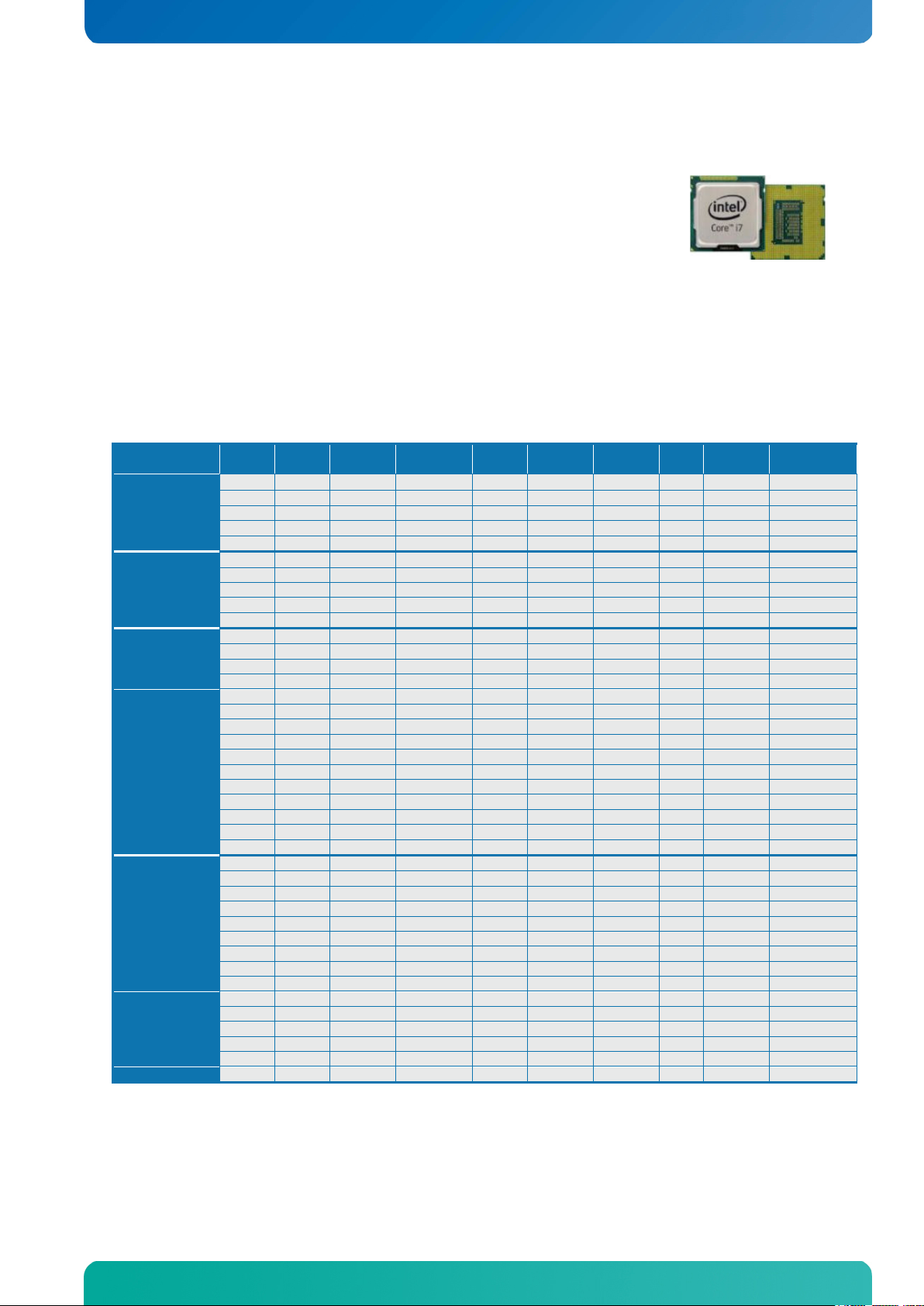
This manual describes the KTQ67/Flex-Medical made by KONTRON T echnology A/S. In this manual
the board will also be denoted KTQ67.
The KTQ67/Flex-Medial is based on the Q67 chipset, s upport 2nd and 3rd generation Int el® i7 -, i5 -,
i3 2Core and 4Core pr ocessor and the Celeron B81 0 2Core, see “Processor Support T able for more
specific details.
Use of this Users Guide implies a basic knowledge of PC-AT hard- and software. This manual is
focused on describ ing the KTQ67 board spec ial features and is not i ntended to be a standard PC-AT
textbook.
New users are recom mended to study the short inst allation procedure stated in th e following chapter
before switching-on the power.
All configuration and setup of the CPU board is either done automaticall y or manually by the user via
the BIOS setup menus. Only exception is the “Load Default BIOS Settings” Jumper.
Page 8
KTQ67/Flex -Medical Users Guide
KTD-N0849-D Page 8
Warning: Turn off PSU (Power Supply Unit) completely (no mains power connected to the
!
!
Warning: When mounting the board to chassis etc. please notice that the board contains
without reasonable care. A damaged component can result in malfunction or no function at all.
Installation procedure
Note: To clear all BIOS settings, including Password protection, activate “Load Default BIOS Settings”
1 Installation procedure
1.1 Installing the board
To get the board running, follow these steps. If the board shipped from KONTRON has already
components like DRAM, CPU and cooler mounted, then relevant steps below, can be skipped.
1. Turn off the PSU (Power Supply Unit)
2. Insert the DRAM(s) (UDIMM 240pin)
Be careful to push it in the slot(s) b efore locking th e tabs. For a list of approved DRAM contact your
Distributor or FAE. See also chapter “System Memory Support”.
3. Install the processor
The CPU is ke yed and will onl y mount in t he CPU sock et in one way. Use finger to open/ close the
CPU socket. Refer to supported processor overview for details.
4. Cooler Installation
Use heat paste or adhesive pads between CPU and cooler and connect the Fan electrically to the
FAN_CPU connector.
5. Connecting Interfaces
Insert all external cables for hard disk , keyboard etc. A monit or must be connected in order to be
able change BIOS settings.
6. Connect and turn on PSU
Connect PSU to the board by the ATX/BTXPWR and the 4-pin ATX+12V connectors.
7. Power Button
The PWRBTN_IN must be toggled to start the Power supply; this is done by shorting pins 16
(PWRBTN_IN) and pin 18 (GND) on the FRONTPNL connector (see Connector description). A
“normally open” switch can be connected via the FRONTPNL connector.
8. BIOS Setup
Enter the BIOS setup by pressing the <Del> key during boot up.
Enter Exit Menu and Load Optimal Defaults.
Refer to the “BIOS Configuration / Setup“ section of this manual for details on BIOS set up .
Jumper for ~10 sec (without power connected).
9. Mounting the board to chassis
When fixing the Motherb oard on a chassis it is recomm ended using screws with integrated washer and
having diameter of ~7mm.
Note: Do not use washers with teeth, as they can damage the PCB and may cause short circuits.
PSU) or leave the Power Connectors unconnected while configuring the board. Otherwise
components (DRAM, LAN cards etc.) might get damaged. Make sure PSU has 3.3V monitoring
watchdog (standard ATX PSU feature), running the board without 3.3V will damage the board
within minutes.
components on both sides of the PCB which can easily be damaged if board is handled
Page 9

KTQ67/Flex -Medical Users Guide
KTD-N0849-D Page 9
ADVARSEL
When an interface/connector has a VCC (or other power) pin, which is directly connected to a power
Installation procedure
1.2 Requirement according to IEC60950
Users of KTQ67 should take care when designing chassis interface connectors in order to fulfil the
IEC60950 standard:
plane like the VCC plane:
To protect the external power lines of the peripheral devices, the customer has to take care about:
• That the wires have suitable rating to withstand the maximum available power.
• That the enclosure of the peripheral device fulfils the fire protecting requirements of IEC60950.
Lithium Battery precautions:
CAUTION!
Danger of explosion if battery is incorrectly
replaced.
Replace only with same or equivalent type
recommended by manufacturer.
Dispose of used batteries according
to the manufacturer’s instructions.
ADVARSEL!
Lithiumbatteri – Eksplosionsfare ved fejlagtig
håndtering.
Udskiftning må kun ske med batteri
af samme fabrikat og type.
Levér det brugte batteri tilbage til leverandøren.
VARNING
Explosionsfara vid felaktigt batteribyte.
Använd samma batterityp eller en ekvivalent
typ som rekommenderas av apparattillverkaren.
Kassera använt batteri enligt fabrikantens
instruktion.
VORSICHT!
Explosionsgefahr bei unsachgemäßem
Austausch der Batterie.
Ersatz nur durch den selben oder einen vom
Hersteller empfohlenen gleichwertigen Typ.
Entsorgung gebrauchter Ba tterie n nach
Angaben des Herstellers.
Eksplosjonsfare ved feilaktig skifte av batteri.
Benytt samme batteritype eller en tilsvarende
type anbefalt av apparatfabrikanten.
Brukte batterier kasseres i henhold til
fabrikantens
instruksjoner.
VAROITUS
Paristo voi räjähtää, jos se on virheellisesti
asennettu.
Vaihda paristo ainoastaan laltevalmistajan
suosittelemaan
tyyppiin. Hävitä käytetty paristo valmistajan
ohjeiden
mukaisesti.
Page 10

KTQ67/Flex -Medical Users Guide
KTD-N0849-D Page 10
Form factor
KTQ67/Flex-Medical: Flex-ATX (190,5 mm by 228, 6 mm)
Processor
Support the following Intel® Core™ processors via Socket H2 (LGA1155), ZIF Sock et
Memory
• 4x DDR3 UDIMM 240pin socket
Chipset
Intel Q67 PCH (Platform Controller Hub)
Security
• Intel® Integrated TPM 1.2 support
Management
• Intel® Active Management T ec hnology (Intel® AMT) 8.0
Audio
Audio, 7.1 Channel High Definition Audio Codec using the VIA 1708B codec
System Specification
2 System Specification
2.1 Component main da ta
The table below summarizes the features of the KTQ67/Flex –Medical embedded motherboard.
• Intel® Core™ i7, 2nd and 3rd Generation
• Intel® Core™ i5, 2nd and 3rd Generation
• Intel® Core™ i3, 2nd and 3rd Generation
• Intel® Pentium® Desktop
• 1066/1333MHz system bus and 3/6/8MB internal cache.
(Intel® Pentium® Desktop G622 only 1066MHz)
• Up to 95W (Thermal Guideline)
• Support single and dual ranks DDR3 1066/1333MT/s
(PC3-8500/PC3-10600)
• Support system memory from 256MB and up to 4x 8GB
Note: Less than 4GB displayed in System Properties using 32bit OS
(Shared Video Memory/PCI resources is subtracted)
• ECC not supported (chipset limitation)
• Intel ® VT-d (Virtualisation Technology for Directed I/O)
• Intel ® TXT (Trusted Execution Technology)
• Intel ® vPRO
• Intel ® AMT (Active Management Technology) version 8
• Intel ® AT (Anti-Theft Technology)
• Intel ® HD Audio Technology
• Intel ® RST (Rapid Storage Technology)
• Intel ® RRT (Rapid Recover Technology)
• SATA (Serial ATA) 6Gb/s and 3Gb/s.
• USB revision 2.0
• PCI Express revision 2.0
• ACPI 3.0b compliant
• Dual Display support (Dual Graphic Pipes)
• Blue-ra y H D video playback
• Line-out
• Line-in
• Surround output: SIDE, LFE, CEN, BACK and FRONT
• Microphone: MIC1 and MIC2
• CDROM in
• SPDIF (electrical Interface only)
• On-board speaker (Electromagnetic Sound Generator like Hycom HY-05LF)
Page 11

KTQ67/Flex -Medical Users Guide
KTD-N0849-D Page 11
Video
Intel ® HD Graphics 4000 or
I/O Control
Via ITE IT8516E Embedded Controller and Winbond W83627DHG I/O Controller
Peripheral
• Six USB 2.0 ports on I/O area
LAN
• 1x 10/100/1000Mbits/s LAN (ETHER1) using Intel® Lewisville 82579LM Gigabit
Expansion
• PCI Bus routed to 2x PCI slots (PCI Local Bus Specification Revision 3.0, 33MHz)
System Specification
Intel ® HD Graphics 3000 or
Intel ® HD Graphics 2500 or
Intel ® HD Graphics 2000 or
Intel ® HD Graphics, depending on actual CPU.
Analogue VGA and digital dis play ports via the Mobile Intel ® Q67 Chipset.
• DVI-I & DVI-D ports via Mobile Intel ® Q67 Chipset. (Digital single channel only).
• LVDS panel support (optional) up to 24 bit, 2 pixels/clock and 1920x1200.
• Dual independent pipes for Mirror and Dual independent display support
(both via LPC Bus interface)
interfaces
Support
Capabilities
• Eight USB 2.0 ports on internal pinrows
• Four Serial ports (RS232) on internal pinrows
• Two Serial ATA-600 IDE interfaces (blue)
• Four Serial ATA-300 IDE interfaces (black)
• RAID 0/1/5/10 support
• mSATA via mSATA connector
• PS/2 keyboard and mouse ports via pinrow
PHY connected to Q67 supporting AMT 8.0. Galvanic Isolated.
• 1x 10/100/1000Mbits/s LAN (ETHER2) using Intel® Hartwell 82574L PCI Express
controller. Galvanic Isolated.
• PXE Netboot supported.
• Wake On LAN (WOL) supported
• PCI-Express slot(s) (PCIe 2.0):
• 1 slot PCIe x16
• 1 slot PCIe x4 (in a x16 slot)
• SMBus, compatible with ACCES BUS and I2C BUS, (via Feature connector)
• SPI bus routed to SPI connector
• DDC Bus routed to DP connector when DP Adapters are connected
• 5 x digital input, (via Feature connector)
• 13 x GPIOs (General Purpose I/Os), (via Feature connector)
• DAC, ADC, PWM and TIMER (Multiplexed), (via Feature connector)
• WAKE UP / Interrupt Inputs (Multiplexed), (via Feature connector)
• 3 Wire Bus for GPIO Expansion (up to 152 GPIOs), (via Feature connector)
• 8 bit Timer output, (via Feature connector)
Page 12

KTQ67/Flex -Medical Users Guide
KTD-N0849-D Page 12
Hardware
• Smart Fan control system, support Thermal® and Speed® cruise for FAN_CPU
Power
Supply Unit
Battery
BIOS
• Kontron Technology / AMI BIOS (EFI c ore vers io n)
Operating
• WinXP (32b *)
System Specification
Monitor
Subsystem
• CPU die temperature input (Precision +/- 3ºC)
• Voltage monitoring
• Intrusion (Case Open) detect input, (via Feature connector)
• Sleep S4/S5# Indication, (via Feature connector)
• System Powergood Signal, (via Feature connector)
ATX/BTX (w. ATX+12V) PSU for full PCI/PCIe load.
Exchangeable 3.0V Lithium battery for on-board Real Time Clock and CMOS RAM.
Manufacturer Panasonic / Part-number CR-2032L/BN, CR2032N/BN or CR-2032L/BE.
Approximate 5 years retention.
Current draw is 5,7µA when PSU is disconnected and 0 µA in S0 – S5.
CAUTION: Danger of explosion if the battery is incorrectly replaced. Replace
only with the same or equivalent type recommended by the manufacturer.
Dispose of used batteries according to th e manufacturer’s instructions.
• Support for ACPI 3.0 ( Advanced Configuration and Power Interface), Plug & Play
o Suspend (S1 mode)
o Suspend To Ram (S3 mode)
o Suspend To Disk (S4 mode)
• “Always On” BIOS power setting
• RAID Support (RAID modes 0,1, 5 and 10)
Systems
Support
• Windows 7 (32b + 64b *)
• WES7 (32b * + 64b *)
• Linux Fedora *
• Linux Ubuntu *
• VxWorks (not ready yet)
*= Out Of The Box installation test only
Page 13

KTQ67/Flex -Medical Users Guide
KTD-N0849-D Page 13
Environmental
System Specification
Conditions
Operating:
0°C – 60°C operating temperature (forced cooling). It is the customer’s
responsibility to provide sufficient airflow around each of the components to keep
them within allowed temperature range.
10% - 90% relative humidity (non-condensing)
Operating altitude: up to 2000 meters
Storage:
-20°C – 70°C; lower limit of storage temperature is defined by specification
restriction of on-board CR2032 battery. Board with battery has been verified for
storage temperature down to -40°C by Kontron.
5% - 95% relative humidity (non-condensing)
Electro Static Discharge (ESD) / Radiated Emissions (EMI): (Pending)
All Peripheral interfaces intended for connection to external equipment are ESD/
EMI protected.
EN 61000-4-2:2000 ESD Immunity
EN55022:1998 class B Generic Emission Standard.
Safety:
IEC 60950-1: 2005, 2nd Edition
UL 60950-1
CSA C22.2 No. 60950-1
Product Category: Information Technology Equipment Including Electrical
Business Equipment
Product Category CCN: NWGQ2, NWGQ8
File number: E194252
Theoretical MTBF:
211.994 / 100.475 hours @ 40ºC / 60ºC for the KTQ67/Flex
Restriction of Hazardous Substances (RoHS):
The KTQ67 is RoHS compliant.
Capacitor utilization:
No Tantalum capacitors on board
Only Japanese brand Solid capacitors rated for 100 ºC used on board
Page 14
KTQ67/Flex -Medical Users Guide
KTD-N0849-D Page 14
System Specification
2.2 System overview
The block diagram below shows the architecture and main components of the KTQ67. The key
component on the board is the Intel
®
Q67 (Cougar Point) Mo bi le Expres s Chipset.
More detailed block diagram on next page.
Page 15
KTQ67/Flex -Medical Users Guide
KTD-N0849-D Page 15
Dual Channel DDR3
PCIe x16 Graphics
Ivy Bridge or
2x DisplayPort
VGA
PCIe x4 Slot
Intel 82574L 10/100/GBe
14x USB
6x SATA
SDVO to LVDS (option)
VIA Codec
SPI
SPI
TPM
Intel Lewisville PHY
System Specification
IO controller
IO controller
PCI slot
PCI slot
COM3/4
COM1/2
FEATURE
FAN CPU/SYS
1067/1333/1600
4 x DIMM
(Gen2.0)
ITE8516
Sandy Bridge
LGA1155
Q67 PCH
W83627DHG-P(T)
Page 16
KTQ67/Flex -Medical Users Guide
KTD-N0849-D Page 16
Processor
Brand
Clock
[GHz]
Turbo
[GHz]
Cores /
Threads
Bus
[MHz]
Cache
[MB]
CPU
Number
sSpec
no.
TG
[W/ºC]
Note
3.5
3.9
4 / 8
1333/1600
8
3770K
SR0PL
E1
77/67.4
HDG4000
I7 3rd Gen.
3.4
3.9
4 / 8
1333/1600
8
3770
SR0PK
E1
77/67.4
HDG4000
(Ivy Bridge)
3.1
3.9
4 / 8
1333/1600
8
3770S
SR0PN
E1
65/69.1
HDG4000
2.5
3.7
4 / 8
1333/1600
8
3770T
SR0PQ
E1
45/69.8
HDG4000
3.5
3.9
4 / 8
1066/1333
8
2700K
SR0DG
D2
95/72.6
HDG3000
I7 2nd Gen.
3.4
3.8
4 / 8
1066/1333
8
2600
SR00B
D2
95/72.6
HDG2000
(Sandy Bridge)
3.4
3.8
4 / 8
1066/1333
8
2600K
SR00C
D2
95/72.6
HDG3000
2.8
3.8
4 / 8
1066/1333
8
2600S
SR00E
D2
65/69.1
HDG2000
3.4
3.8
4 / 4
1333/1600
6
3570
SR0T7
N0
77/67.4
HDG2500
I5 3rd Gen.
3.4
3.8
4 / 4
1333/1600
6
3570K
SR0PM
E1
77/67.4
HDG4000
(Ivy Bridge)
3.3
3.7
4 / 4
1333/1600
6
3550
SR0P0
E1
77/67.4
HDG2500
3.2
3.6
4 / 4
1333/1600
6
3470
SR0T8
N0
77/67.4
HDG2500
3.1
3.8
4 / 4
1333/1600
6
3570S
SR0T9
N0
65/69.1
HDG2500
3.1
3.5
4 / 4
1333/1600
6
3450
SR0PF
E1
77/67.4
HDG2500
3.1
3.3
4 / 4
1333/1600
6
3350P
SR0WS
E1
69/67.4 -
3.0
3.7
4 / 4
1333/1600
6
3550S
SR0P3
E1
65/69.1
HDG2500
3.0
3.2
4 / 4
1333/1600
6
3330
SR0RQ
E1
77/67.4
HDG2500
2.9
3.6
4 / 4
1333/1600
6
3475S
SR0PP
E1
65/69.1
HDG4000
2.9
3.6
4 / 4
1333/1600
6
3470S
SR0TA
N0
65/69.1
HDG2500
2.9
3.6
2 / 4
1333/1600
3
3470T
SR0RJ
L1
35/65.0
HDG2500 *
2.8
3.5
4 / 4
1333/1600
6
3450S
SR0P2
E1
65/69.1
HDG2500
2.7
3.5
4 / 4
1333/1600
6
3330S
SR0RR
E1
65/
HDG2500
2.3
3.2
4 / 4
1333/1600
6
3570T
SR0P1
E1
45/69.8
HDG2500
3.3
3.7
4 / 4
1066/1333
6
2550K
SR0QH
D2
95/72.6
-
I5 2nd Gen.
3.3
3.7
4 / 4
1066/1333
6
2500K
SR008
D2
95/72.6
HDG3000
(Sandy Bridge)
3.3
3.7
4 / 4
1066/1333
6
2500
SR00T
D2
95/72.6
HDG2000
3.2
3.5
4 / 4
1066/1333
6
2450P
SR0G1
D2
95/72.6
-
3.1
3.4
4 / 4
1066/1333
6
2380P
SR0G2
D2
95/72.6 -
3.1
3.4
4 / 4
1066/1333
6
2400
SR00Q
D2
95/72.6
HDG2000
3.0
3.3
4 / 4
1066/1333
6
2320
SR02L
D2
95/72.6
HDG2000
2.9
3.2
4 / 4
1066/1333
6
2310
SR02K
D2
95/72.6
HDG2000
2.8
3.1
4 / 4
1066/1333
6
2300
SR00D
D2
95/72.6
HDG2000
2.7
3.7
4 / 4
1066/1333
6
2500S
SR009
D2
65/69.1
HDG2000
2.7
3.5
2 / 4
1066/1333
3
2390T
SR065
Q0
35/65.0
HDG2000
2.5
3.3
4 / 4
1066/1333
6
2405S
SR0BB
D2
65/69.1
HDG3000
2.5
3.3
4 / 4
1066/1333
6
2400S
SR00S
D2
65/69.1
HDG2000
2.3
3.3
4 / 4
1066/1333
6
2500T
SR00A
D2
45/69.8
HDG2000
System Specification
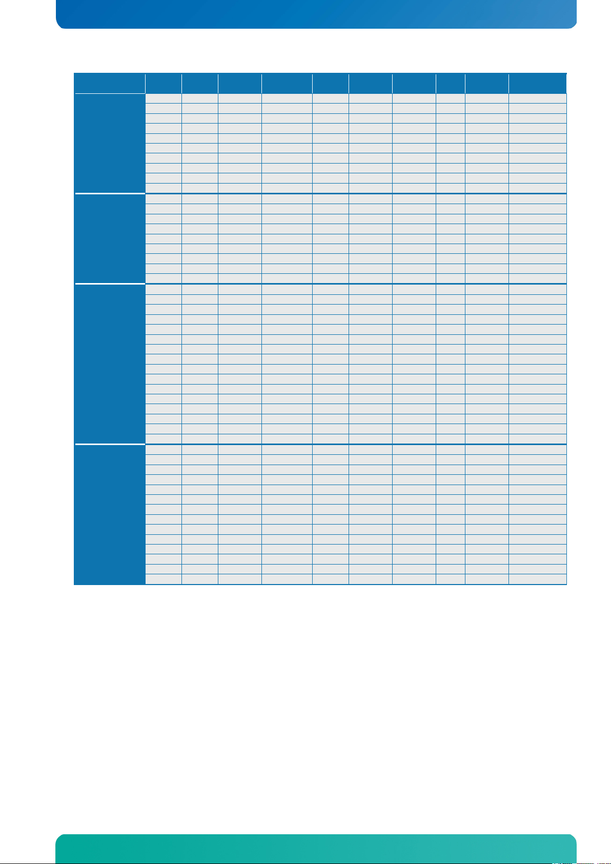
2.3 Processor Suppor t Table
The KTQ67 is designed to support the following LGA1155 processors (up to 95W power consumption):
nd
and 3rd generation Intel® Core™ i7 processor
2
nd
2
and 3rd generation Intel® Core™ i5 processor
nd
2
and 3rd generation Intel® Core™ i3 processor
Pentium and Celeron
In the following list you will find all CPU’s supported by the chipset in according to Intel. Please notice
that Bus speed 1600 MHz has not been verified yet.
Embedded CPU’s are indic ated by green text, success fully tested CPU’s are indicated by highlighted
text, successfully tested embedded CPU’s are indicated by green and highlighted text and failed
CPU’s are indicated by red text.
Some processors in the l ist are distributed from Kontron, thos e CPU’s are marked by an * (asterisk ).
However please notice that this marking is only guide line and maybe not fully updated.
Step
Page 17
KTQ67/Flex -Medical Users Guide
KTD-N0849-D Page 17
Processor
Brand
Clock
[GHz]
Turbo
[GHz]
Cores /
Threads
Bus
[MHz]
Cache
[MB]
CPU
Number
sSpec
no.
TG
[W/ºC]
Note
3.5 - 2 / 4
1333/1600
3
3250
SR0YX
P0
55/65.3
HDG2500
I3 3rd Gen.
3.4 - 2 / 4
1333/1600
3
3245
SR0YL
L1
55/65.3
HDG4000
(Ivy Bridge)
3.4 - 2 / 4
1333/1600
3
3240
SR0RH
L1
55/65.3
HDG2500
3.3 - 2 / 4
1333/1600
3
3225
SR0RF
L1
55/65.3
HDG4000
(No vPRO)
3.3 - 2 / 4
1333/1600
3
3220
SR0RG
L1
55/65.3
HDG2500
3.2 - 2 / 4
1333/1600
3
3210
SR0YY
P0
55/65.3
HDG2500
3.0 - 2 / 4
1333/1600
3
3250T
SR0YW
P0
35/65.0
HDG2500
2.9 - 2 / 4
1333/1600
3
3240T
SR0RK
L1
35/65.0
HDG2500
2.8 - 2 / 4
1333/1600
3
3220T
SR0RE
L1
35/65.3
HDG2500
3.4 - 2 / 4
1066/1333
3
2130
SR05W
Q0
65/69.1
HDG2000
I3 2nd Gen.
3.3 - 2 / 4
1066/1333
3
2125
SR0AY
J1
65/69.1
HDG3000
(Sandy Bridge)
3.3 - 2 / 4
1066/1333
3
2120
SR05Y
Q0
65/69.1
HDG2000
3.1 - 2 / 4
1066/1333
3
2105
SR0BA
J1
65/69.1
HDG3000
(No vPRO)
3.1 - 2 / 4
1066/1333
3
2100
SR05C
Q0
65/69.1
HDG2000
3.1 - 2 / 4
1066/1333
3
2102
SR05D
Q0
65/69.1
HDG2000
2.6 - 2 / 4
1066/1333
3
2120T
SR060
Q0
35/65.0
HDG2000
2.5 - 2 / 4
1066/1333
3
2100T
SR05Z
Q0
35/65.0
HDG2000
3.1 - 2 / 2
1066/1333
3
G870
SR057
Q0
65/69.1
HDG
3.0 - 2 / 2
1066/1333
3
G860
SR058
Q0
65/69.1
HDG
Pentium
2.9 - 2 / 2
1066/1333
3
G850
SR05Q
Q0
65/69.1
HDG
2.9 - 2 / 2
1066
3
G645
SR0RS
Q0
65/69.1
HDG
2.8 - 2 / 2
1066/1333
3
G840
SR05P
Q0
65/69.1
HDG
2.8 - 2 / 2
1066
3
G640
SR059
Q0
65/69.1
HDG
2.7 - 2 / 2
1066
3
G632
SR05N
Q0
65/69.1
HDG
2.7 - 2 / 2
1066
3
G630
SR05S
Q0
65/69.1
HDG
2.8 - 2 / 2
1066/1333
3
G860T
SR0MF
Q0
35/65.0
HDG
2.6 - 2 / 2
1066
3
G620
SR05R
Q0
65/69.1
HDG
2.6 - 2 / 2
1066
3
G622 - -
65/69.1
HDG
2.5 - 2 / 2
1066
3
G645T
SR0S0
Q0
35/65.0
HDG
2.4 - 2 / 2
1066
3
G640T
SR066
Q0
35/65.0
HDG
2.2 - 2 / 2
1066
3
G620T
SR05T
Q0
35/65.0
HDG
2.3 - 2 / 2
1066
3
G630T
SR05U
Q0
35/65.0
HDG
2.7 - 2 / 2
1333
2
G1620
SR10L
P0
55
HDG *
2.7 - 2 / 2
1066
2
G555
SR0RZ
Q0
65/69.1
HDG
2.6 - 2 / 2
1333
2
G1610
SR10K
P0
55
HDG *
2.6 - 2 / 2
1066
2
G550
SR061
Q0
65/69.1
HDG
2.5 - 2 / 2
1066
2
G540
SR05J
Q0
65/69.1
HDG
Celeron
2.4 - 2 / 2
1066
2
G530
SR05H
Q0
65/69.1
HDG
2.3 - 2 / 2
1333
2
G1610T
SR10M
P0
35/
HDG *
2.2 - 2 / 2
1066
2
G550T
SR05V
Q0
35/65.0
HDG
2.1 - 2 / 2
1066
2
G540T
SR05L
Q0
35/65.0
HDG
2.0 - 2 / 2
1066
2
G530T
SR05K
Q0
35/65.0
HDG
2.0 - 1 / 2
1066/1333
1.5
G470
SR0S7
Q0
35/65.5
HDG
1.8 - 1 / 2
1066
1.5
G460
SR0GR
Q0
35/65.5
HDG
1.6 - 1 / 1
1066
1
G440
SR0BY
Q0
35/65.5
HDG
System Specification
Step
(*) ECC not supported on KTQ67.
Not all CPUs, even of s ame type, support a ll functions ex . i7 3770K, i7 2600K, i5 3570K, 3450, 3450S,
3350P, 3330S, 3330 and i5 2500K, 2300, 2310, 232 0, 2380P, 2450P , 2550K doesn’t sup port vPro while
all other i7 and i5 does.
Most of the proces sors are supportin g the Enhance d Intel® SpeedStep® which is impr oved SpeedSt ep
technology for faster transition between voltage (power saving states) and frequency states with the
result of improved power/performance balance. For more details see http://ark.intel.com
Intel® Turbo Boost T echnology 2.0 is sup ported by i5 and i7, as indicated in above l ist of processors,
and is enabling overclocking of all cores, when operated within the limits of thermal design power,
temperature and current.
Page 18
KTQ67/Flex -Medical Users Guide
KTD-N0849-D Page 18
!
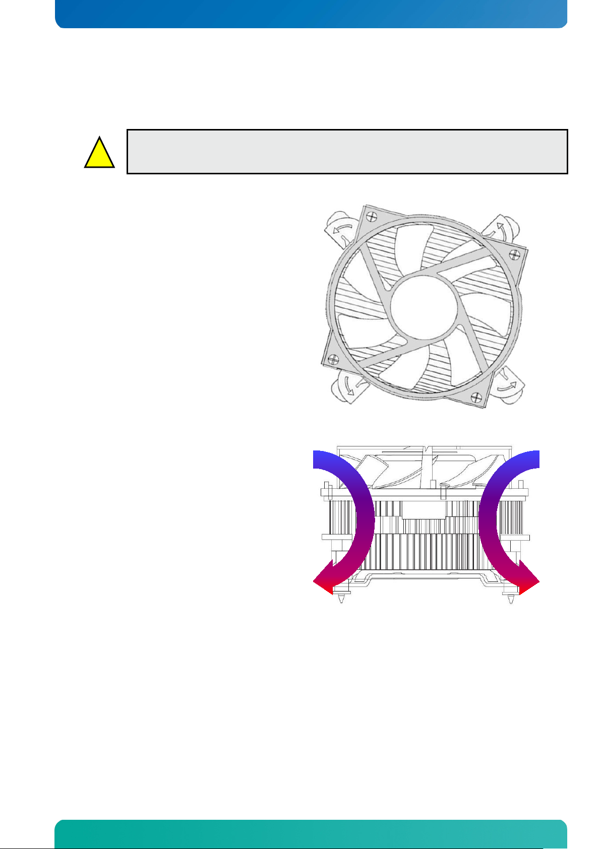
Warning: Make sure sufficient airflow is always present around the components located below
or is blocking the airflow around these components, causing reduced lifetime.
It is recommended to use a cooler like the Kontron
Components below the cooler
Note: The temperature of the air blown out of the cooler should be 70ºC maximum.
System Specification
Sufficient cooling must be applied to the CPU in order to remove the effect as listed in above table
(Thermal Guideline). The sufficient cooling is also depending on the maximum (worst-case) ambient
operating temperature and the actual load of processor.
PN 1046-6305 “KTQ67 Cooler”.
the cooler. Different coolers are available on the market and some is not generating any airflow
The design of this cooler makes sure airflow is
always present around the components below the
cooler. Even if Fan is set to be off, it is still running
a minimum RPM (Rotation Per Minute).
Air sucked in to the cooler
Air blown out of the cooler
Page 19
KTQ67/Flex -Medical Users Guide
KTD-N0849-D Page 19
DIMM Type
Module
Memory
[Mill/s]
Processor
[MHz]
Resulting
[MHz]
Peak transfer
[MB/s]
DDR3 1066
PC3-8500
1066
1066 / 1333
533
8533
DDR3 1333
PC3-10600
1333
1333
666
10666
DDR3 1600
PC3-12800
1600
1333
666
10666
DDR3 (SLOT B1)
System Specification
It has not been verified that the combination of CPU
2.4 System Memor y support
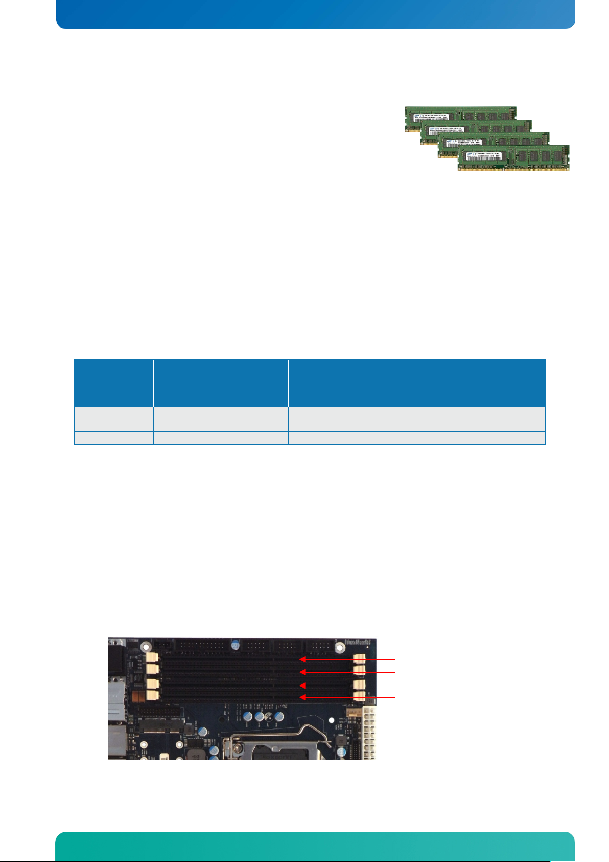
The KTQ67/Flex-Medical has four DDR3 UDIMM sockets. The sockets support the following memory
features:
• 4x DDR3 1.5V UDIMM 240-pin
• Dual-channel with 2 UDIMM per channel
• Single/dual rank unbuffered 1066/1333MT/s (PC3-8500/PC3-10600)
From 256MB and up to 4x 8GB.
Note: Less than 4GB displayed in System Properties using 32bit OS
(Shared Video Memory/PCI resources is subtracted)
• SPD timings supported
• ECC not supported
The installed DDR3 DIMM should suppor t the S erial P resence De tect (SPD) data structure. T his all ows
the BIOS to read and configure the m emory controller for optimal perf ormance. If non-SPD memory is
used, the BIOS will attem pt to configure the memory settings, but perfor mance and reliability may be
impacted.
Memory Operating Frequencies
Regardless of the DIMM type used, the memory frequency will either be equal to or less than the
processor system bus frequency. For example, if DDR3 1600 m emor y is used with a 1333 M H z s ys te m
bus frequency processor, the m emory clock will op erate at 666 MHz. The table below lists the res ulting
operating memory frequencies based on the combination of DIMMs and processors.
name
transfers
Notes: Kontron offers the following memory modules:
1054-2766 1GB DDR3 1066
1031-9872 1GB DDR3 1333
1054-3706 1GB DDR3 1600
1054-2768 2GB DDR3 1066
1054-3702 2GB DDR3 1333
1054-3707 2GB DDR3 1600
1054-3700 4GB DDR3 1066
1054-3703 4GB DDR3 1333
1054-3708 4GB DDR3 1600
1054-3704 8GB DDR3 1333
1052-5601 8GB DDR3 1600
Data
supporting Bus Speed 1600 MHz and DDR3 1600 actually
runs at 1600 MHz.
In order to support Intel ® AMT (Management Engine) SLOT
A0 must always be populated. In case of using more than a
single DIMM it is recommended to popula te A0 + B0 fir st.
system bus
frequency
memory clock
frequency
DDR3 (SLOT B0)
DDR3 (SLOT A1)
DDR3 (SLOT A0)
(Example Flex version)
rate
Page 20

KTQ67/Flex -Medical Users Guide
KTD-N0849-D Page 20
System Specification
2.5 KTQ67 Graphics Subsystem
The KTQ67 support Intel ® HD Graphic s 4000, 3000, 2500, 2000 or Intel ® HD G raphics , depend ing on
actual CPU. However pleas e notice that even tho ugh an I vy Bridg e CPU s upporting T riple In dependent
Displays are used then on the KTQ67 only Dual Independent Displays are supported.
Supports 2x DVI (single channel) via DVI-I and DVI-D connector and opt ion al ly LVDS .
Up to two displays (any two display outputs) can be activated at the same time and be used to
implement dual independ e nt dis p lay support or mirror display suppor t. PCIe a nd PCI graphics cards can
be used to replace on-board graphics or in combination with on-board graphics.
2.5.1 Intel® HD Graphics 3000 (example)
Features of the Intel HD Graphics 3000 build into the i3, i5 and i7 processors, includes:
• High quality graphics engine supporting
o DirectX10.1 and OpenGL 3.0 compliant
o Shader Model 4.1 support
o Intel ® Clear Video HD Technology
o Intel ® Quick Sync Video Technology
o Intel ® Flexible Display Interface (Intel ® FDI)
o Core frequency of 350 - 1300 (Turbo) MHz
o Memory Bandwidth up to 21.3 GB/s
o 12 3D Execution Units
o 1.62 GP/s and 2.7 GP/S pixel rate (DP outputs)
o Hardware Acceleration full MPEG2, full VC-1 and full AVC
o Dynamic Video Memory Technology (DVMT) support up to 1720 MB
• LVDS panel Support (optional), 18/24 bit colours in up to WUXGA (1920x1200) @60 Hz and
SPWG (VESA) colour coding. OpenLDI (JEIDA) colour coding is 18 bit with or without Dit her ing.
Page 21
KTQ67/Flex -Medical Users Guide
KTD-N0849-D Page 21
Supply
Min
Max
Note
ATX supplies
KTQ67
PSU
Gnd
Current
Probe
Tektronix TDS5104B
System Specification
2.6 Power Consumption
In order to ensure safe operation of the board, the ATX12V power supply must monitor the supply
voltage and shut do wn if the supplies are out of ran ge – refer to the har dware manual for the actual
power supply specification. The KTQ67 board is powered through the ATX/BTX connector and
ATX+12V connector. Both connectors must be used in according to the ATX12V PSU standard.
The requirements to the supply voltages are as follows:
VCC3.3 3.135V 3.465V
Vcc 4.75V 5.25V
+12V 11.4V 12.6V
–12V –13.2V –10.8V
-5V -5,50V -4.5V Not required for the KTQ67 board
5VSB 4.75V 5.25V
More detailed Static Power Consumption
On the following pages the power consumption of the KTQ67 Board is measured under:
1- DOS, idle, mean
2- Windows7, Running 3DMARK 2005 & BiT 6, mean
3- S1, mean
4- S3, mean
5- S4, mean
The following items were used in the test setup:
Low Power Setup
Standard system conf iguration equipped with PCI card, Internal graphics , 2x SATA disks, Intel i3
CPU, 2x DIMM (1GB Modules), CRT Monitor, Keyboard & Mouse. 1x 1-4GB USB Flash Stick.
High Power Setup
Standard system configuration equipped with PCI card, PCIex4, PCIex16, miniPCIe WLAN, 4x
SATA disks, Intel i7 C PU, 4x DIMM (2+2+2+1 Modul es), CRT Monitor, Keyboard & Mous e, 4x 14GB USB Flash Stick.
1. 12V active cooler (Intel BOX).
2. USB Keyboard/Mouse Genius
3. CRT Sampo AlphaScan 912
4. 2.5” HDD Fujitsu MHY2120BH
5. ATX Fortron 400W
6. Tektronix TDS5104B
7. Tektronix TCPA300
8. Tektronix TCP312
9. Fluke 289
10. ATX rail switch
Note: The Power consumption of Display and HD are not included.
Should be ±5% for compliance with the ATX specification
Should be ±5% for compliance with the ATX specification.
Should be minimum 5.00V measured at USB connectors
in order to meet the requirements of USB standard.
Should be ±5% for compliance with the ATX specification
Should be ±10% for compliance with the ATX specification
Should be ±5% for compliance with the ATX specification
Page 22
KTQ67/Flex -Medical Users Guide
KTD-N0849-D Page 22
DOS Idle, Mean, No external load
Supply
Current draw
Power consumption
+12V
0.258A
3.096W
+12V P4
1.363A
16.366W
+5V
1.417A
7.083W
+3V3
0.490A
1.618W
-12V
0.035A
0.416W
5VSB
0.006A
0.030W
Total
28.6W
Windows 7, mean
3DMARK2005 (first scene) & BiT 6
Supply
Current draw
Power consumption
+12V
0.293A
3.516W
+12V P4
2.642A
31.702W
+5V
2.170A
10.850W
+3V3
0.443A
1.463W
-12V
0.037A
0.442W
5VSB
0.006A
0.030W
Total
48.0W
S1 Mode, Mean, No external load
Supply
Current draw
Power consumption
+12V
0.212A
2.540W
+12V P4
0.238A
2.854W
+5V
0.828A
4.140W
+3V3
0.265A
0.878W
-12V
0.039A
0.469W
5VSB
0.006A
0.030W
Total
10.9W
S3 Mode, Mean, No external load
Supply
Current draw
Power consumption
+12V
0A
0W
+12V P4
0A
0W
+5V
0A
0W
+3V3
0A
0W
-12V
0A
0W
5VSB
0.153A
0.765W
Total
0.77W
S4 Mode, Mean, No external load
Supply
Current draw
Power consumption
+12V
0A
0W
+12V P4
0A
0W
+5V
0A
0W
+3V3
0A
0W
-12V
0A
0W
5VSB
0.120A
0.600W
Total
0.60W
System Specification
Low Power Setup results:
Page 23

KTQ67/Flex -Medical Users Guide
KTD-N0849-D Page 23
DOS Idle, Mean, No external load
Supply
Current draw
Power consumption
+12V
1.978A
23.737W
+12V P4
1.827A
21.924W
+5V
2.061A
10.306W
+3V3
1.032A
3.404W
-12V
0.032A
0.384W
5VSB
0.006A
0.030W
Total
59.8W
Windows 7, mean
3DMARK2005 (first scene) & BiT 6
Supply
Current draw
Power consumption
+12V
3.115A
37.380W
+12V P4
4.957A
59.484W
+5V
2.457A
12.285W
+3V3
1.659A
5.475W
-12V
0.038A
0.456W
5VSB
0.006A
0.030W
Total
115.1W
S1 Mode, Mean, No external load
Supply
Current draw
Power consumption
+12V
2.179A
26.144W
+12V P4
0.594A
7.128W
+5V
1.076A
5.380W
+3V3
1.348A
4.447W
-12V
0.043A
0.516W
5VSB
0.006A
0.030W
Total
43.6W
S3 Mode, Mean, No external load
Supply
Current draw
Power consumption
+12V
0A
0W
+12V P4
0A
0W
+5V
0A
0W
+3V3
0A
0W
-12V
0A
0W
5VSB
0.364A
1.820W
Total
1.82W
S4 Mode, Mean, No external load
Supply
Current draw
Power consumption
+12V
0A
0W
+12V P4
0A
0W
+5V
0A
0W
+3V3
0A
0W
-12V
0A
0W
5VSB
0.295A
1.475W
Total
1.48W
System Specification
High Power Setup results:
Page 24
KTQ67/Flex -Medical Users Guide
KTD-N0849-D Page 24
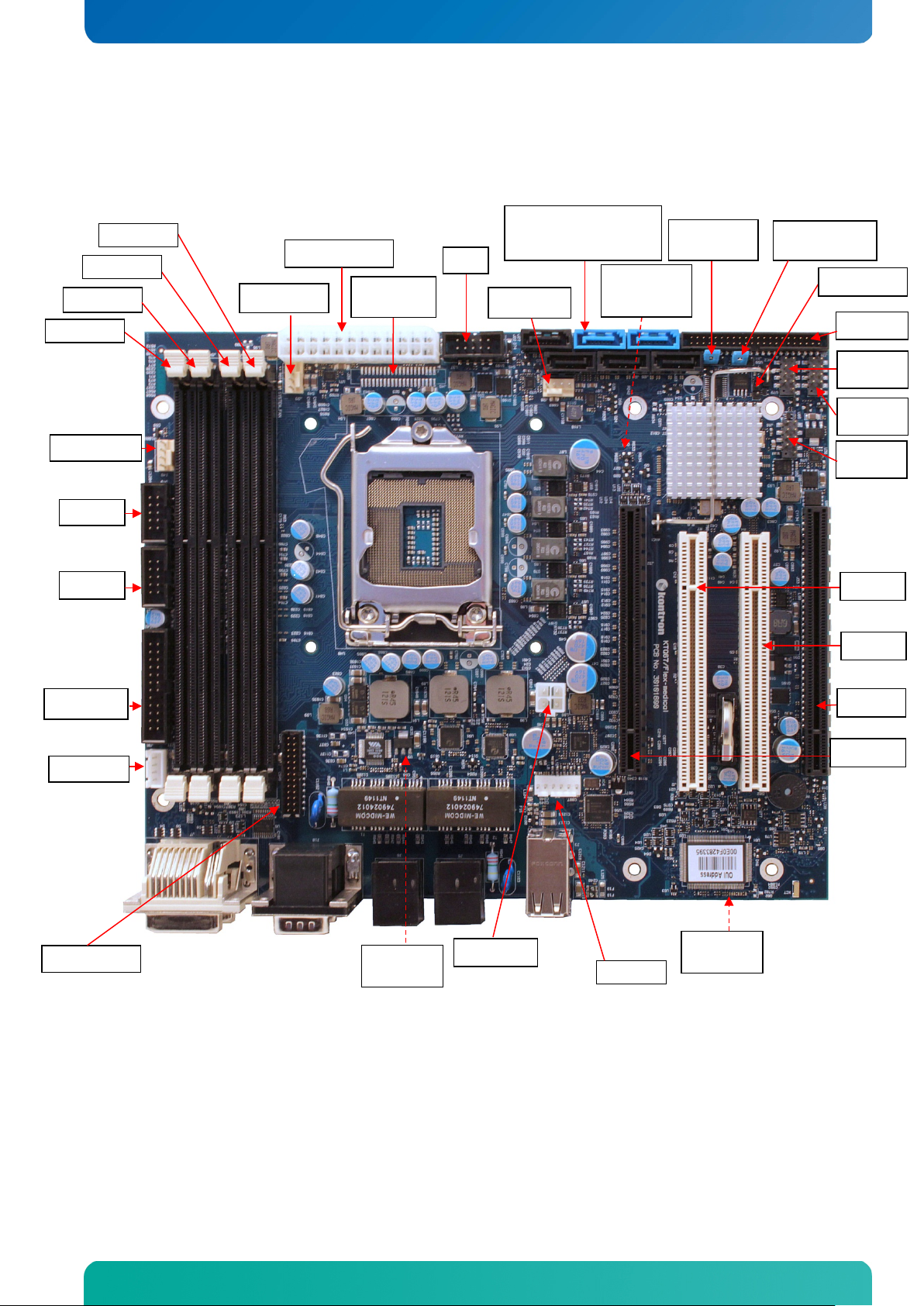
Connector Location
DDR3 B0
Feature
PCIex16
ATX/ BTXPWR
USB12
Frontpanel
FAN_SYS2
Audioheader
COM3
PWRBTN
ATX+12V
FAN_SYS1
FAN_CPU
COM4
PCI0
Load Default
BIOS Settings
Sata5 - Sata0 - Sata1
(see note)
LVDS
(optionally)
PCIex4
SPI recover
SPI
Notes: Sata0/Sata1support up to 6GB/s and Sata2/Sata3/Sata4/Sata5 support up to 3GB/S.
XDP-PCH
(see note)
PCI1
USB8
USB10
J12
(not used)
LPT
(see note)
XDP-CPU
(see note)
3 Connector Locations
3.1 KTQ67/Flex-Medical – frontside
Sata2 - Sata3 - Sata4
(backside)
The LPT connector and the XDP connectors are not mounted in volume production.
Page 25
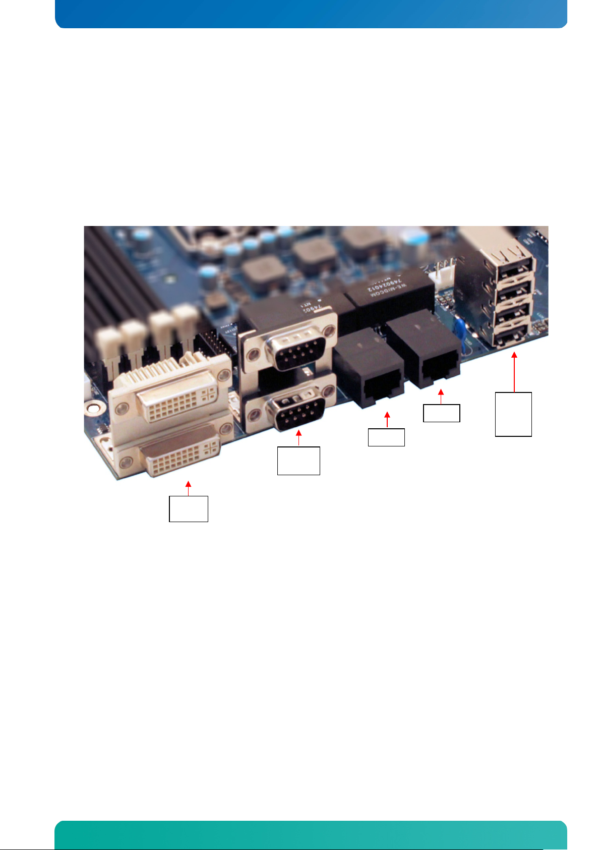
KTQ67/Flex -Medical Users Guide
KTD-N0849-D Page 25
DVI-D
DVI-I
USB0
USB3
ETH2
COM1
COM2
ETH1
Connector Location
USB1
USB2
Page 26

KTQ67/Flex -Medical Users Guide
KTD-N0849-D Page 26
Connector Definitions
4 Connector Definitions
The following sections provide pin definitions and detailed description of all on-board connectors.
The connector definitions follow the following notation:
Column
name
Pin Shows the pin-numbers in the connector. The graphical layout of the connector definition
Signal The mnemonic name of the signal at the current pin. The notation “XX#” states that the
Type AI: Analogue Input.
Ioh: Typical current in mA flowing out of an output pin through a grounded load, while the
Pull U/D On-board pull-up or pull-down resistors on input pins or open-collector output pins.
Note Special remarks concerning the signal.
The abbreviation TBD is used for specifications which are not available yet or which are not sufficiently
specified by the component vendors.
Description
tables is made similar to the physical connectors.
signal “XX” is active low.
AO: Analogue Output.
I: Input, TTL compatible if nothing else stated.
IO: Input / Output. TTL compatible if nothing else stated.
IOT: Bi-directional tristate IO pin.
IS: Schmitt-trigger input, TTL compatible.
IOC: Input / open-collector Output, TTL compatible.
IOD: Input / Output, CMOS level Schmitt-triggered. (Open drain output)
NC: Pin not connected.
O: Output, TTL compatible.
OC: Output, open-collector or open-drain, TTL compatible.
OT: Output with tri-state capability, TTL compatible.
LVDS: Low Voltage Differential Signal.
PWR: Power supply or ground reference pins.
output voltage is > 2.4 V DC (if nothing else stated).
Iol: Typical current in mA flowing into an output pin from a VCC connected load, while the
output voltage is < 0.4 V DC (if nothing else stated).
Page 27
KTQ67/Flex -Medical Users Guide
KTD-N0849-D Page 27
3
TMDS Data 2/4 Shield
PWR
6
DDC Clock
DDC Clock
IO
2K2
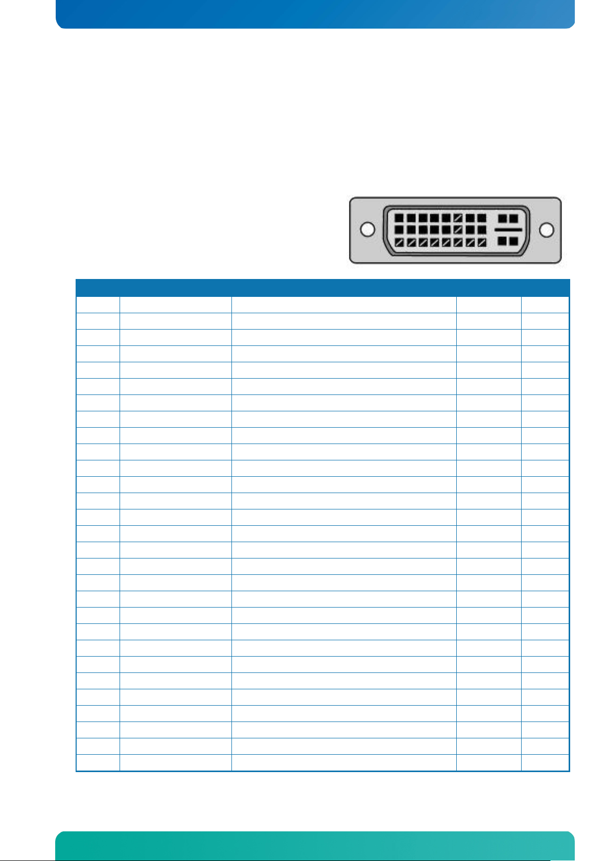
IO-Area Connectors
The DVI-I connector is based on stacked DVI-I
5 IO-Area Connectors
5.1 Display connectors (IO Area)
The KTQ67/Flex-Medical has two DVI connectors (stac ked) and optionally one on-board LVDS panel
interface. Both DVI c onnec tors support s ing le chann el dig ital si gnals in a D VI-I typ e connec tor. On ly the
lower DVI connector s upport also analogue sig nals. Two gra phic pipes are suppor ted; meaning tha t up
to two independent displays can be implemented using any two of the above mentioned graphic ports.
5.1.1 DVI (lower) connector – DVI-I
connector type Kycon KVI42X-DA29S-S-A4N-W or
similar. The lower connector is supporting both
analogue and digital (single channel) signals.
Pin No. Signal Description Type Pull Up
1 TMDS Data 2- Digital Red – (Link 1) LVDS OUT
2 TMDS Data 2+ Digital Red + (Link 1) LVDS OUT
4 N.C. -
5 N.C. -
7 DDC Data DDC Data IO 2K2
8 VSYNC AI
9 TMDS Data 1- Digital Green – (Link 1) LVDS OUT
10 TMDS Data 1+ Digital Green + (Link 1) LVDS OUT
11 TMDS Data 1/3 Shield PWR
12 N.C. -
13 N.C. -
14 +5V (55mA) Power for monitor when in standby PWR
15 GND PWR
16 Hot Plug Detect Hot Plug Detect I
17 TMDS Data 0- Digital Blue – (Link 1) / Digital sync LVDS OUT
18 TMDS Data 0+ Digital Blue + (Link 1) / Digital sync LVDS OUT
19 TMDS Data 0/5 Shield PWR
20 N.C. -
21 N.C. -
22 TMDS Clock Shield PWR
23 TMDS Clock+ Digital clock + (Link 1) LVDS OUT
24 TMDS Clock- Digital clock - (Link 1) LVDS OUT
C1 RED AI
C2 GREEN AI
C3 BLUE AI
C4 HSYNC AI
C5 GND PWR
Page 28
KTQ67/Flex -Medical Users Guide
KTD-N0849-D Page 28
Pin No.
Signal
Description
Type
Pull Up
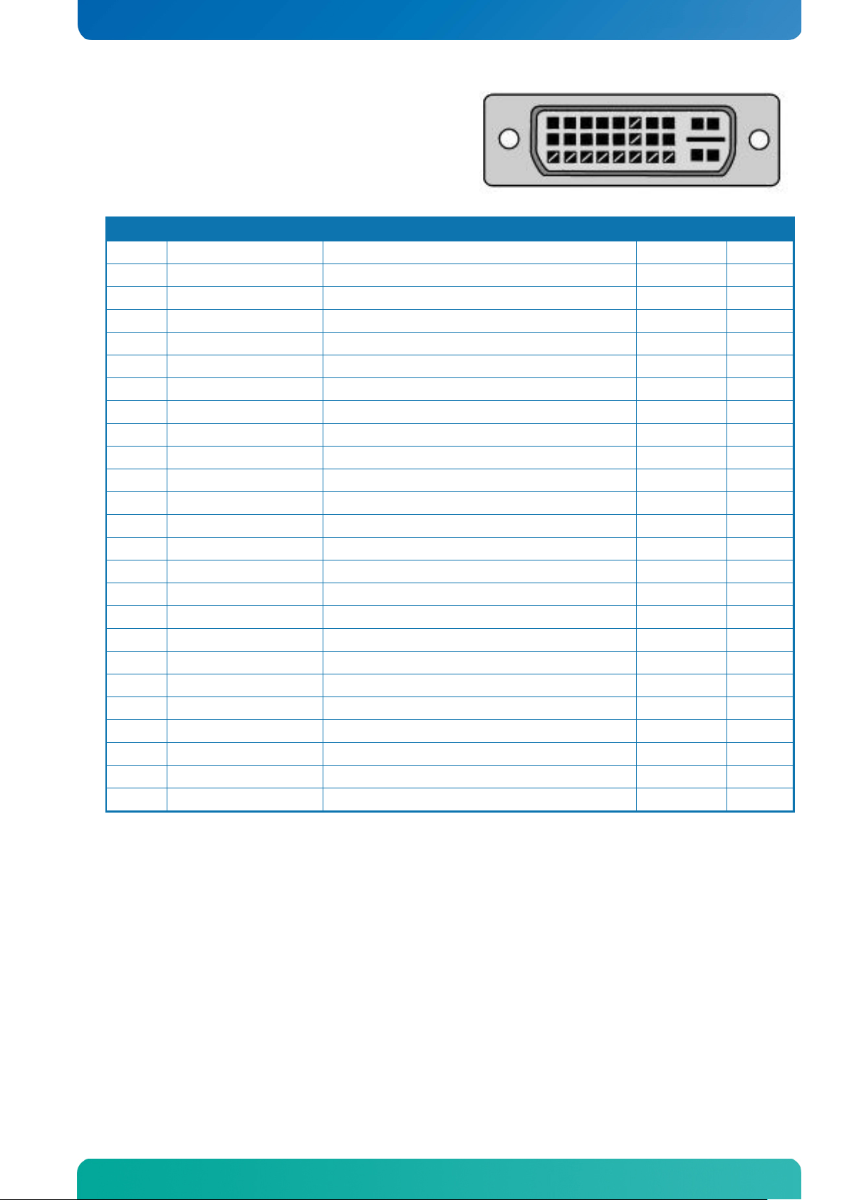
IO-Area Connectors
The DVI-I connector is based on stacked DVI-I
5.1.2 DVI-D (upper) connector – DVI-D
connector type Kycon KVI42X-DA29S-S-A4N-W or
similar. It is supporting only digital signals (single
channel).
1 TMDS Data 2- Digital Red – (Link 1) LVDS OUT
2 TMDS Data 2+ Digital Red + (Link 1) LVDS OUT
3 TMDS Data 2/4 Shield PWR
4 N.C. -
5 N.C. -
6 DDC Clock DDC Clock IO 2K2
7 DDC Data DDC Data IO 2K2
8 N.C. -
9 TMDS Data 1- Digital Green – (Link 1) LVDS OUT
10 TMDS Data 1+ Digital Green + (Link 1) LVDS OUT
11 TMDS Data 1/3 Shield PWR
12 N.C. -
13 N.C. -
14 +5V (55mA) Power for monitor when in standby PWR
15 GND PWR
16 Hot Plug Detect Hot Plug Detect I
17 TMDS Data 0- Digital Blue – (Link 1) / Digital sync LVDS OUT
18 TMDS Data 0+ Digital Blue + (Link 1) / Digital sync LVDS OUT
19 TMDS Data 0/5 Shield PWR
20 N.C. -
21 N.C. -
22 TMDS Clock Shield PWR
23 TMDS Clock+ Digital clock + (Link 1) LVDS OUT
24 TMDS Clock- Digital clock - (Link 1) LVDS OUT
C1 - C5 N.C. -
Page 29
KTQ67/Flex -Medical Users Guide
KTD-N0849-D Page 29
Signal
PIN
Type
Ioh/Iol
Note
MDI3-
MDI3+
MDI1-
MDI2-
MDI2+
MDI1+
MDI0-
MDI0+
1 2 3 4 5 6 7 8
IO-Area Connectors
5.2 Ethernet Connect ors (IO Area)
The KTQ67/Flex-Medical support two channels of 10/100/1000Mb Ethernet ports, ETH1 and ETH2.
Both ports are Galvanic Is olated. ETH 1 (left Ethernet connec tor) is based on Intel® Lewisville 82579LM
Gigabit PHY with AMT 8.0 support and ETH2 (right Ethernet connector) is based on Intel® Hartwell
82574L PCI Express controller.
In order to achieve the specified performance of the Ethernet port, minimum Category 5 twisted pair
cables must be used with 10/100MB and minimum Category 5E, 6 or 6E with 1Gb LAN networks.
The signals for the Ethernet ports are as follows:
Signal Description
MDI[0]+ / MDI[0]- In MDI mode, this is the first pair in 1000Base-T, i.e. the BI_DA+/- pair, and is
the transmit pair in 10Base-T and 100Base-TX.
In MDI crossover mode, this pair acts as the BI_DB+/- pair, and is the receive
pair in 10Base-T and 100Base-TX.
MDI[1]+ / MDI[1]- In MDI mode, this is the second pair in 1000Base-T, i.e. the BI_DB+/- pair, and
is the receive pair in 10Base-T and 100Base-TX.
In MDI crossover mode, this pair acts as the BI_DA+/- pair, and is the transmit
pair in 10Base-T and 100Base-TX.
MDI[2]+ / MDI[2]-
In MDI mode, this is the third pair in 1000Base-T, i.e. the BI_DC+/- pair.
In MDI crossover mode, this pair acts as the BI_DD+/- pair.
MDI[3]+ / MDI[3]-
Note: MDI = Media Dependent Interface.
The pinout of the RJ45 connectors is as follows:
In MDI mode, this is the fourth pair in 1000Base-T, i.e. the BI_DD+/- pair.
In MDI crossover mode, this pair acts as the BI_DC+/- pair.
Page 30
KTQ67/Flex -Medical Users Guide
KTD-N0849-D Page 30
Note
Type
Signal
PIN
Signal
Type
Note
1 PWR
5V/SB5V
1 2 3 4 GND
PWR
IO
USB0-
USB0+
IO
1 PWR
5V/SB5V
1 2 3 4 GND
PWR
IO
USB1-
USB1+
IO
1 PWR
5V/SB5V
1 2 3 4 GND
PWR
IO
USB2-
USB2+
IO
1 PWR
5V/SB5V
1 2 3 4 GND
PWR
IO
USB3-
USB3+
IO
Signal
Description
IO-Area Connectors
5.3 USB Connectors (IO Area)
The KTQ67/Flex-Medical board contains two EHCI (Enhanced Host Controller Interface) host
controllers (EHCI 1 and EHCI2) that support u p to fourteen USB 2.0 port s, twelve are available on the
KTQ67/Flex-Medical. The USB2.0 ports allowing data transfers up to 480Mb/s and legacy
Keyboard/Mouse and wakeup from sleep states are supported. Over-current detection on all fourteen
USB ports is supported. The following USB connectors are available in the IO Area.
USB Port 0 - 3 (all via EHCI1) are supplied on the combined USB0, USB1, USB2 and USB3 connector.
Note: It is required to use only HiSpeed USB cable, specified in USB2.0 standard:
5.3.1 USB Connector 0/1/2/3 (USB0/1/2/3)
USB Ports 0, 1, 2 and 3 are mounted in a common stack connector.
Note 1: In order to meet the requirements of USB standard, the 5V input supply must be at least 5.00V.
USB0+ USB0USB1+ USB1-
USB2+ USB2USB3+ USB3-
5V/SB5V
Differential pair works as Data/Address/Command Bus.
5V supply for external devices. SB5V is supplied during powerdown to allow
wakeup on USB device activity. Protected by resettable 1A fuse for each USB ports.
Page 31

KTQ67/Flex -Medical Users Guide
KTD-N0849-D Page 31
Pull
U/D
Pull
U/D
- -
PWR
GND
5 9 RI I -
/5K - O DTR
4 8 CTS I -
/5K - O TxD
3 7 RTS O - /5K - I
RxD
2 6 DSR I -
/5K
/5K - I
DCD
1
IO-Area Connectors
5.4 COM1 and COM2 Connectors (IO Area)
Four RS232 serial ports are available on the KTQ67/Flex-Medical, COM1 and COM2 are available in
the IO Area while the other COM ports are available on internal pin header connectors.
The typical definition of the signals in the COM ports is as follows:
Signal Description
TxD Transmitted Data, sends data to the communications link. The signal is set to the marking
state (-12V) on hardware reset when the transmitter is empty or when loop mode operation is
initiated.
RxD Received Data, receives data from the communications link.
DTR Data Terminal Ready, indicates to the modem etc. that the on-board UART is ready to
establish a communication link.
DSR Data Set Ready, indicates that the modem etc. is ready to establish a communications link.
RTS Request To Send, indicates to the modem etc. that the on-board UART is ready to exchange
data.
CTS Clear To Send, indicates that the modem or data set is ready to exchange data.
DCD Data Carrier Detect, indicates that the modem or data set has detected the data carrier.
RI Ring Indicator, indicates that the modem has received a ringing signal from the telephone line.
The pinout of Serial ports COM1 is as follows:
Note
Ioh/Iol Type Signal PIN Signal Type Ioh/Iol
Note
Page 32

KTQ67/Flex -Medical Users Guide
KTD-N0849-D Page 32
Note
Type
Signal
PIN
Signal
Type
Note
PWR
3V3
12
24 GND
PWR
PWR
+12V
11
23 5V
PWR
PWR
+12V
10
22 5V
PWR
PWR
SB5V
9
21 5V
PWR I P_OK
8
20 -5V
PWR 1
PWR
GND
7
19 GND
PWR
PWR
5V
6
18 GND
PWR
PWR
GND
5
17 GND
PWR
PWR
5V
4
16 PSON#
OC
PWR
GND
3
15 GND
PWR
PWR
3V3
2
14 -12V
PWR
PWR
3V3
1
13 3V3
PWR
Note
Type
Signal
PIN
Signal
Type
Note
PWR
GND
2 4
+12V
PWR 1
PWR
GND
1 3
+12V
PWR
1
P_OK is a power good signal and should be asserted high by the power supply to indicate
Internal Connectors
6 Internal Connectors
6.1 Power Connector (ATX/BTXPWR)
The KTQ67 boar d is designed to be supplie d from a standard AT X (or BTX) power supply. Use of BT X
supply is not required for operation, but may be required to drive high-power PCIe cards.
ATX/ BTX Power Connector (J45):
Note 1: -5V supply is not used on-board.
See chapter “Power Consumption” regard ing input tolerances o n 3.3V, 5V, SB5V, +1 2 and -12V (also
refer to ATX specification version 2.2).
ATX+12V-4pin Power Connector (J46):
Note 1: Use of the 4-pin ATX+12V Power Connector is required.
Signal Description
P_OK
PS_ON# Active low open drain signal from the board to the power supply to turn on the power supply
that the +5VDC and +3.3VDC outputs are above the undervoltage thresholds of the power
supply. When this signal is asserted high, there should be sufficient energy stored by the
converter to guarantee continuous power operation within specification. Conversely, when
the output voltages fall below the undervoltage threshold, or when mains power has been
removed for a time sufficiently long so that power supply operation is no longer guaranteed,
P_OK should be de-asserted to a low state. The recommended electrical and timing
characteristics of the P_OK (PWR_OK) signal are provided in the ATX12V Power
SupplyDesign Guide.
It is strongly recommended to use an ATX or BTX supply in order to implement the
supervision of the 5V and 3V3 supplies. These supplies are not supervised on-board.
outputs. Signal must be pulled high by the power supply.
Page 33

KTQ67/Flex -Medical Users Guide
KTD-N0849-D Page 33
Pull
U/D
1 CONTROL
O - - 2 SENSE
I
-
4K7 3 +12V
PWR
- -
4 GND
PWR
- -
Pull
U/D
-
2 SENSE
I
-
4K7 3 +12V
PWR
- -
4 GND
PWR
- -
Internal Connectors
6.2 Fan Connectors (FAN_CPU) (J28) and (FAN_SYS) (J29)
The FAN_CPU is used for the connection of the FAN for the CPU.
The FAN_SYS can be used to power, control and monitor a fan for chassis ventilation etc.
The 4pin header is recommended to be used for driving 4-wire type Fan in order to implement FAN
speed control. 3-wire Fan is also possible, but no fan speed control is integrated.
4-pin Mode:
PIN Signal Type Ioh/Iol
Signal Description
CONTROL PWM signal for FAN speed control
SENSE Tacho signal from the fan for supervision. The signals shall be generated by an open
collector transistor or similar. On-board is a pull-up resistor 4K7 to +12V. The signal has to
be pulsed, typically twice per rotation.
12V +12V supply for fan. A maximum of 2000mA can be supplied from this pin.
GND Power Supply GND signal
3-pin Mode:
PIN Signal Type Ioh/Iol
Note
Note
Signal Description
SENSE Tacho signal from the fan for supervision. The signals shall be generated by an open
collector transistor or similar. On-board is a pull-up resistor 4K7 to +12V. The signal has to
be pulsed, typically twice per rotation.
12V +12V supply for fan. A maximum of 2000mA can be supplied from this pin.
GND Power Supply GND signal
Page 34

KTQ67/Flex -Medical Users Guide
KTD-N0849-D Page 34
Pull
U/D
1 KBDCLK
IOD
/14mA
2K7
2 KBDDAT
IOD
/14mA
2K7
3 MSCLK
IOD
/14mA
2K7
4 MSDAT
IOD
/14mA
2K7
5 5V/SB5V
PWR
- -
6
GND
PWR
- -
Internal Connectors
6.3 PS/2 Keyboard and Mouse connector ( KBDMSE) (J15)
Attachment of a PS/2 keyboard/mouse can be done through the pinrow connector KBDMSE (J15).
Both interfaces utilize open-drain signalling with on-board pull-up.
The PS/2 mouse and keyboard is supplied from SB5V when in standby mode in order to enable
keyboard or mouse ac tivity to bring the system out from power saving states. T he supply is provided
through a 1.1A resettable fuse.
PIN Signal Type Ioh/Iol
Signal Description – Keyboard & and mouse Connector (KBDMSE).
Signal Description
MSCLK Bi-directional clock signal used to strobe data/commands from/to the PS/2 mouse.
MSDAT Bi-directional serial data line used to transfer data from or commands to the PS/2 mouse.
KDBCLK Bi-directional clock signal used to strobe data/commands from/to the PC-AT keyboard.
KBDDAT
Bi-directional serial data line used to transfer data from or commands to the PC-AT
keyboard.
Note
Page 35

KTQ67/Flex -Medical Users Guide
KTD-N0849-D Page 35
Note
Type
Signal
PIN
Signal
Type
Note
Max. 0.5A
PWR
+12V
1 2 +12V
PWR
Max. 0.5A
Max. 0.5A
PWR
+12V
3 4 +12V
PWR
Max. 0.5A
Max. 0.5A
PWR
+12V
5 6 GND
PWR
Max. 0.5A
Max. 0.5A
PWR
+5V
7 8 GND
PWR
Max. 0.5A
Max. 0.5A
PWR
LCDVCC
9 10 LCDVCC
PWR
Max. 0.5A
2K2Ω, 3.3V
OT
DDC CLK
11
12 DDC DATA
OT
2K2Ω, 3.3V
3.3V level
OT
BKLTCTL
13
14 VDD ENABLE
OT
3.3V level
3.3V level
OT
BKLTEN#
15
16 GND
PWR
Max. 0.5A
LVDS
LVDS A0-
17
18 LVDS A0+
LVDS
LVDS
LVDS A1-
19
20 LVDS A1+
LVDS
LVDS
LVDS A2-
21
22 LVDS A2+
LVDS
LVDS
LVDS ACLK-
23
24 LVDS ACLK+
LVDS
LVDS
LVDS A3-
25
26 LVDS A3+
LVDS
Max. 0.5A
PWR
GND
27
28 GND
PWR
Max. 0.5A
LVDS
LVDS B0-
29
30 LVDS B0+
LVDS
LVDS
LVDS B1-
31
32 LVDS B1+
LVDS
LVDS
LVDS B2-
33
34 LVDS B2+
LVDS
LVDS
LVDS BCLK-
35
36 LVDS BCLK+
LVDS
LVDS
LVDS B3-
37
38 LVDS B3+
LVDS
Max. 0.5A
PWR
GND
39
40 GND
PWR
Max. 0.5A
Signal
Description
LVDS A0..A3
LVDS A Channel data
LVDS ACLK
LVDS A Channel clock
LVDS B0..B3
LVDS B Channel data
LVDS BCLK
LVDS B Channel clock
BKLTCTL
Backlight control (1), PWM signal to implement voltage in the range 0-3.3V
BKLTEN#
Backlight Enable signal (active low) (2)
VDD ENABLE
Output Display Enable.
VCC supply to the display. Power-on/off sequencing depending on selected (in BIOS
setup) display type. 5V or 3.3V selected in BIOS setup. Maximum load is 1A.
DDC CLK
DDC Channel Clock
Internal Connectors
Internal Connectors
6.4 Display connectors (Internal)
The KTQ67 provides optionally interna l on-board LVDS panel interface. For IO Area Display Connectors
(DVI-D and DVI-I), see earlier section.
Two graphic pipes are supported; meaning that up to two independent displays can be im plemented
using any two display connectors in IO Area - and Internal (LVDS) connector (optionally).
6.4.1 LVDS Flat Panel Connector (LVDS) (J39) (optionally)
Two graphic pipes are supported; meaning that up to two independent displays can be implemented
using any two of display connectors (IO Area - and Internal connectors).
Note: The KTQ67 on-board LVDS connector supports single/dual c hannel, 18/ 24bit S PWG panels up
to resolution 1600x1200 or 1920x1080 (1920x1200 with limited frame rate is possible).
Signal Description – LVDS Flat Pan el Con nec tor:
LCDVCC
Notes: Windows API will be availab le to operate the BKLTCTL signal. Some Invert ers have a limited
voltage range 0- 2.5V for this signal: If voltage is > 2.5V the Inverter might latch up. Some
Inverters generates n oise on the BKLTCTL signal, res ulting in making the LVDS transm ission
failing (corrupted pic ture on the displa y). By adding a 1K ohm resistor in series with this signal,
mounted in the Inverter end of the cable kit, the noise is limited and the picture is stable.
If the Backlight Enable is required to be active high, then check the following BIOS Chipset
setting: Backlight Signal Inversion = Enable d.
Page 36

KTQ67/Flex -Medical Users Guide
KTD-N0849-D Page 36
Pull
U/D
1
GND
PWR - - 2
SATA* TX+
3
SATA* TX-
4
GND
PWR - - 5
SATA* RX-
6
SATA* RX+
7
GND
PWR - -
Signal
Description
Host receiver differential signal pair
Internal Connectors
6.5 SATA (Serial ATA) Disk interface (J22 – J27)
The KTQ67 board has an integrated SATA Host controller (integrated in the PCH) that supports
independent DMA operation on six ports. One device can be installed on each port for a maximum of six
SATA devices. A point-to-point interface (SATA cable) is used for host to device connections. Data
transfer rates of up to 6.0G b/s ( typically 600MB/s) on SATA0 and SATA1 (blue connectors) and 3.0Gb/s
(typically 300MB/s) on SATA2, SAT A3, SATA4 an d SATA5 (black c onnectors). In case m SATA is used
then the SATA2 is disabled.
The SATA controller supports:
2 to 6-drive RAID 0 (data striping)
2-drive RAID 1 (data mirroring)
3 to 6-drive RAID 5 (block-level striping w ith par ity).
4-drive RAID 10 (data striping and mirroring)
2 to 6-drive matrix RAID (different parts of a single drive can be assigned to different RAID
devices).
AHCI (Advanced Host Controller Interface)
NCQ (Native Command Queuing). NCQ is for faster data access.
Hot Swap
Intel® Rapid Recover Technology
2 – 256TB volume (Data volumes only)
Capacity expansion
TRIM in Windows 7 (in AHCI and RAID m ode for drives not part of a RAID volum e). (TRIM is for
SSD data garbage handling).
The RAID (Redundant Array of Inde pendent Drives) functionality is based on a firmware system with
support for RAID modes 0 1, 5 and 10.
SATA connector pinning:
The pinout of SATA ports SATA0 (J27), SATA1 (J26), SATA2 (J25), SATA3 (J24), SATA4 (J23) and
SATA5 (J22) is as follows:
PIN Signal Type Ioh/Iol
The signals used for the primary SATA hard disk interface are the following:
SATA* RX+
SATA* RX-
SATA* TX+
SATA* TX-
“*” specifies 0, 1, 2, 3, 4, 5 depending on SATA port.
Host transmitter differential signal pair
Note
Page 37

KTQ67/Flex -Medical Users Guide
KTD-N0849-D Page 37
Note
Type
Signal
PIN
Signal
Type
Note
1
PWR
5V/SB5V
1 2 5V/SB5V
PWR 1
IO
USB8-
3 4 USB9-
IO
IO
USB8+
5 6 USB9+
IO
PWR
GND
7 8 GND
PWR
NC
KEY
9 10 NC
NC
Internal Connectors
Connector Definitions
6.6 USB Connectors (USB)
The KTQ67 board conta ins two EHC I (Enhance d Host C ontroller Int erface) host controllers (EHCI1 a nd
EHCI2) that support up to fourteen USB 2.0 ports allowing data transfers up to 480Mb/s. Legacy
Keyboard/Mouse and wakeup from sleep states are supported. Over-current detection on all fourteen
USB ports is supported. The following USB ports are available on Internal Pinrows:
USB Port 6 and 7 (v ia EHC I1) are supplied on the USB6/7 internal pinrow FRONTPNL connector.
USB Port 8 and 9 (v ia EH CI2) are supplied on the USB8/9 internal pinrow connector.
USB Port 10 and 11 (via EHCI2) are supplied on the USB10/11 internal pinrow connector.
USB Port 12 and 13 (via EHCI2) are supplied on the USB12/13 internal pinrow connector.
Note: It is required to use only HiSpeed USB cable, specified in USB2.0 standard:
6.6.1 USB Connector 6/7
See Frontpanel Connector (FRONTPNL) description.
6.6.2 USB Connector 8/9 (USB8/9) (J18)
USB Ports 8 and 9 are supplied on the internal USB8/9 pinrow connector J18.
Signal Description
USB8+ USB8USB9+ USB9-
5V/SB5V
Differential pair works as Data/Address/Command Bus.
5V supply for external devices. SB5V is supplied during powerdown to allow
wakeup on USB device activity. Protected by resettable 1A fuse covering both USB
ports.
Page 38

KTQ67/Flex -Medical Users Guide
KTD-N0849-D Page 38
Note
Type
Signal
PIN
Signal
Type
Note
1
PWR
5V/SB5V
1 2 5V/SB5V
PWR 1
IO
USB10-
3 4 USB11-
IO
IO
USB10+
5 6 USB11+
IO
PWR
GND
7 8 GND
PWR
NC
KEY
9 10 NC
NC
Signal
Description
Note
Type
Signal
PIN
Signal
Type
Note
1
PWR
5V/SB5V
1 2 5V/SB5V
PWR 1
IO
USB12-
3 4 USB13-
IO
IO
USB12+
5 6 USB13+
IO
PWR
GND
7 8 GND
PWR
NC
KEY
9 10 NC
NC
Internal Connectors
6.6.3 USB Connector 10/11 (USB10/11) (J17)
USB Ports 10 and 11 are supplied on the internal USB10/11 pinrow connector J17.
USB10+ USB10USB11+ USB11-
5V/SB5V
Differential pair works as Data/Address/Command Bus.
5V supply for external devices. SB5V is supplied during powerdown to allow
wakeup on USB device activity. Protected by resettable 1A fuse covering both USB
ports.
6.6.4 USB Connector 12/13 (USB12/13) (J16)
USB Ports 12 and 13 are supplied on the internal USB12/13 pinrow connector J16.
Signal Description
USB12+ USB12USB13+ USB13-
5V/SB5V
Note 1: In order to meet the requirements of USB standard, the 5V input supply must be at least 5.00V.
Differential pair works as Data/Address/Command Bus.
5V supply for external devices. SB5V is supplied during powerdown to allow
wakeup on USB device activity. Protected by resettable 1A fuse covering both USB
ports.
Page 39

KTQ67/Flex -Medical Users Guide
KTD-N0849-D Page 39
Note
Ioh/Iol
Type
Signal
PIN
Signal
Type
Ioh/Iol
Note
- I
DCD
1 2 DSR I - - I
RxD
3 4 RTS O O
TxD
5 6 CTS I - O
DTR
7 8 RI I - - PWR
GND
9 10 5V
PWR - 1
Internal Connectors
6.7 Serial COM3 – COM4 Ports (J20, J21)
Three RS232 serial ports are available on the KTQ67 via pin-row connector. (COM1 and COM2 are in
the IO area and is based on standard DB9 connector, see other section for more info).
The typical definition of the signals in the COM ports is as follows:
Signal Description
Transmitted Data, sends data to the communications link. The signal is set to the marking
TxD
RxD Received Data, receives data from the communications link.
DTR
DSR Data Set Ready, indicates that the modem etc. is ready to establish a communications link.
RTS
CTS Clear To Send, indicates that the modem or data set is ready to exchange data.
DCD Data Carrier Detect, indicates that the modem or data set has detected the data carrier.
The pinout of Serial ports COM3 (J19) and COM4 (J21) is as follows:
state (-12V) on hardware reset when the transmitter is empty or when loop mode operation is
initiated.
Data Terminal Ready, indicates to the modem etc. that the on-board UART is ready to
establish a communication link.
Request To Send, indicates to the modem etc. that the on-board UART is ready to exchange
data.
RI Ring Indicator, indicates that the modem has received a ringing signal from the telephone line.
Note 1: The COM3 and COM4 5V supply is fused with common 1.1A resettable fuse.
DB9 adapter cables (PN 821016 200mm long and 821017 100m m long) are available for implementing
standard COM ports on chassis.
Page 40

KTQ67/Flex -Medical Users Guide
KTD-N0849-D Page 40
Note
Type
Signal
PIN
Signal
Type
Note
AO
LFE-OUT
1 2 CEN-OUT
AO
PWR
AAGND
3 4 AAGND
PWR
AO
FRONT-OUT-L
5 6 FRONT-OUT-R
AO
PWR
AAGND
7 8 AAGND
PWR
AO
REAR-OUT-L
9 10 REAR-OUT-R
AO
AO
SIDE-OUT-L
11
12 SIDE-OUT-R
AO
PWR
AAGND
13
14 AAGND
PWR
AI
MIC1-L
15
16 MIC1-R
AI
PWR
AAGND
17
18 AAGND
PWR LINE1-L
19
20 LINE1-R
NC
NC
21
22 AAGND
PWR
PWR
GND
23
24 NC
NC O SPDIF-OUT
25
26 GND
PWR
Internal Connectors
Internal Connectors
6.8 Audio Connector
The on-board Audio circuit implem ents 7.1+2 Ch annel H igh Def inition Aud io with UAA (Un iversal Au dio
Architecture), featuring five 24-bit stereo DACs and three 20-bit stereo ADCs.
6.8.1 Line2 and Mic2
Line2 and Mic2 are accessible via Front Panel Connector, see Front Panel connector description.
6.8.1 Audio Header Connector (AUDIO_HEAD) (J47)
Signal Description
FRONT-OUT-L Front Speakers (Speaker Out Left).
FRONT-OUT-R Front Speakers (Speaker Out Right).
REAR-OUT-L Rear Speakers (Surround Out Left).
REAR-OUT-R
SIDE-OUT-L
SIDE-OUT-R Side speakers (Surround Out Right)
CEN-OUT
LFE-OUT
NC No connection
MIC1 MIC Input 1
LINE1 Line 1 signals
F-SPDIF-OUT S/PDIF Output
AAGND Audio Analogue ground
Rear Speakers (Surround Out Right).
Side speakers (Surround Out Left)
Center Speaker (Center Out channel).
Subwoofer Speaker (Low Freq. Effect Out).
Page 41

KTQ67/Flex -Medical Users Guide
KTD-N0849-D Page 41
Pull
U/D
1
PWRBTN_IN#
I
-
1K1 2 GND
PWR
- -
3 PWR_LED
O
-
470 4
SLEEP_LED
O
-
470
Internal Connectors
6.9 Power Button Connector (PWRBTN) (J48)
Signal Description
PWRBTN_IN# Power Button In. Toggle this signal low to start the ATX/TX PSU and boot the board.
PWR_LED PoWeR LED, active high (+5V via 470Ω).
SLEEP_LED Sleep LED, active high (+5V via 470Ω).
PIN Signal Type Ioh/Iol
Note
Page 42

KTQ67/Flex -Medical Users Guide
KTD-N0849-D Page 42
Pull
U/D
Ioh/
Iol
Ioh/
Iol
Pull
U/D
- -
PWR
USB6/7_5V
1 2 USB6/7_5V
PWR - - - - USB6-
3 4 USB7-
- - - - USB6+
5 6 USB7+
- - - -
PWR
GND
7 8 GND
PWR - - - -
NC
NC
9 10 LINE2-L
- - - -
PWR
+5V
11
12 +5V
PWR - - - /7mA
O
SATA_LED#
13
14 SUS_LED
O
7mA - - - PWR
GND
15
16 PWRBTN_IN#
I 1K1
4K7 - I
RSTIN#
17
18 GND
PWR - - - -
PWR
SB3V3
19
20 LINE2-R
- - - -
PWR
AGND
21
22 AGND
PWR - - - -
AI
MIC2-L
23
24 MIC2-R
AI - -
5V supply for external devices. SB5V is supplied during power down to allow
Internal Connectors
6.10 Front Panel Connector (FRONTPNL) (J36)
Note
Signal Description
USB10/11_5V
USB1+
USB1-
wakeup on USB device ac t i vit y. Protec t ed by resettable 1.1A fuse c over ing both U SB
ports.
Universal Serial Bus Port 1 Differentials: Bus Data/Address/Command Bus.
Type Signal PIN Signal Type
Note
USB3+
USB3-
+5V
SATA_LED#
SUS_LED Suspend Mode LED (active high signal). Output 3.3V via 470Ω.
PWRBTN_IN#
RSTIN#
LINE2
MIC2
SB3V3 Standby 3.3V voltage
AGND
Note: In order to meet the requirements of USB standard, the 5V input supply must be at least 5.00V.
Universal Serial Bus Port 3 Differentials: Bus Data/Address/Command Bus.
Maximum load is 1A or 2A per pin if us ing IDC c on nector flat cable or crim p term inals
respectively.
SATA Activit y L ED , act ive l ow signa l (via 470Ω). Reco mmended is using Low Power
LED like HLMP47 00 with anode connected to +5V (pin 11). When red c olor LED is
used, possible weak glowing could be noticed when the LED supposed to be of f. In
order to eliminate th is problem a resistor 3K3 can be connected in parallel with the
LED or a diode can be connected in series with the LED.
Power Button In. Toggle this signal low to start the ATX / BTX PSU and boot the
board.
Reset Input. When pull ed lo w f or a m inimum 16ms, the reset process wil l be initiated.
The reset process continues even though the Reset Input is kept low.
Line2 is second stereo Line signals
MIC2 is second stereo microphone input.
Analogue Ground for Audio
Page 43

KTQ67/Flex -Medical Users Guide
KTD-N0849-D Page 43
Pull
U/D
Pull
U/D
2
2M/ - I
CASE_OPEN#
1 2 SMBC
/4mA
10K/ 1 - 25/25mA O S5#
3 4 SMBD
/4mA
10K/ 1 - 25/25mA
O
PWR_OK
5 6 EXT_BAT
PWR - - - O FAN3OUT
7 8 FAN3IN
I - - - -
PWR
SB3V3
9 10 SB5V
PWR - - -
IOT
GPIO0
11
12 GPIO1
IOT - -
IOT
GPIO2
13
14 GPIO3
IOT - -
IOT
GPIO4
15
16 GPIO5
IOT - -
IOT
GPIO6
17
18 GPIO7
IOT - - -
PWR
GND
19
20 GND
PWR - - - I GPIO8
21
22 GPIO9 I - - I
GPIO10
23
24 GPIO11
I - - I GPIO12
25
26 GPIO13
IOT - -
IOT
GPIO14
27
28 GPIO15
IOT - -
IOT
GPIO16
29
30 GPIO17
IOT - - -
PWR
GND
31
32 GND
PWR - - - 8/8mA
O
EGCLK
33
34 EGCS#
O
8/8mA
- - 8/8mA EGAD
35
36 TMA0 O - PWR
+12V
37
38 GND
PWR - - - O FAN4OUT
39
40 FAN4IN
I - - - -
PWR
GND
41
42 GND
PWR - - - -
PWR
GND
43
44 S3#
O
25/25mA
-
CASE OPEN, used to det ec t if the s ystem c ase has been ope ned. T his sign al’s s tatus
is readable, so it may be used like a GPI when the Intruder switch is not required.
PoWeR OK, signal is h igh if no power failures ar e detected. (This is not the same as
the P_OK signal generated by ATX PSU).
(EXTernal BATtery) o ption for c onnecting + t erm inal of an ex tern al prim a r y cell ba tter y
charging and can be used with or without the on-board battery installed.
General Purpose Inputs / Output. These Signals may be controlled or monitored
through the use of the KT-API-V2 (Application Programming Interface).
Internal Connectors
6.11 Feature Connector (FEATURE) (J30)
Note
Notes: 1. Pull-up to +3V3Dual (+3V3 or SB3V3). 2. Pull-up to on-board Battery.
Signal Description
Ioh/Iol Type Signal PIN Signal Type Ioh/Iol
Note
CASE_OPEN#
SMBC SMBus Clock signal
SMBD SMBus Data signal
S3#
S5# S5 sleep mode, active low output, optionally used to deactivate external system.
PWR_OK
EXT_BAT
FAN3OUT FAN 3 speed control OUTput, 3.3V PWM signal can be used as Fan control voltage.
FAN3IN FAN3 Input. 0V to +3V3 amplitude Fan 3 tachometer input.
FAN4OUT FAN 4 speed control OUTput, 3.3V PWM signal can be used as Fan control voltage.
FAN4IN FAN4 Input. 0V to +3V3 amplitude Fan 3 tachometer input.
SB3V3 Max. load is 0.75A (1.5A < 1 sec.)
SB5V StandBy +5V supply.
GPIO0..17
EGCLK Extend GPIO Clock signal
EGAD Extend GPIO Address Data signal
EGCS# Extend GPIO Chip Select signal, active low
TMA0 Timer Output
+12V Max. load is 0.75A (1.5A < 1 sec.)
S3 sleep mode, active low output, optionally used to deactivate external system.
(2.5 - 3.47 V) (– term inal connecte d to GND) . T he external bat tery is prot ected ag ainst
Page 44

KTQ67/Flex -Medical Users Guide
KTD-N0849-D Page 44
GPIO0
DAC0/GPJ0
AO/IOS
GPIO1
DAC1/GPJ1
AO/IOS
GPIO2
DAC2/GPJ2
AO/IOS
GPIO3
DAC3/GPJ3
AO/IOS
GPIO4
PWM2/GPA2
O8/IOS
GPIO5
PWM3/GPA3
O8/IOS
GPIO6
PWM4/GPA4
O8/IOS
GPIO7
PWM5/GPA5
O8/IOS
GPIO8
ADC0/GPI0
AI/IS
GPIO9
ADC1/GPI1
AI/IS
GPIO10
ADC2/GPI2
AI/IS
GPIO11
ADC3/GPI3
AI/IS
GPIO12
ADC4/WUI28/GPI4
AI/IS/IS
GPIO13
RI1#/WUI0/GPD0
IS/IS/IOS
GPIO14
RI2#/WUI1/GPD1
IS/IS/IOS
GPIO15
TMRI0/WUI2/GPC4
IS/IS/IOS
GPIO16
TMRI1/WUI3/GPC6
IS/IS/IOS
GPIO17
L80HLAT/BAO/WUI24/GPE0
O4/O4/IS/IOS
Internal Connectors
GPIO in more details.
The GPIO’s are contro lled vi a the ITE IT 8516F Em bedded Contr oll er. Eac h GPIO has 100pF t o ground,
clamping Diode to 3V3 and has m ultiplexed functionalit y. Some pins can be DAC (Digital to Analogue
Converter output), PWM (Pulse Width Modulated signal output), ADC (Analogue to Digital Converter
input), TMRI (Tim er Counter Input), WUI (Wake Up Input), RI (Ring Indicator Input) or some special
function.
Signal IT8516F pin name Type Description
Page 45

KTQ67/Flex -Medical Users Guide
KTD-N0849-D Page 45
Warning: Don’t leave the jumper in position 1-2, otherwise if power is disconnected,
the battery will fully deplete within a few weeks.
J11
Pin3
Pin2
Pin1
•
•
• • •
J12
Pin3
Pin2
Pin1
•
•
• • •
Internal Connectors
!
Jumper (in Load Default BIOS Settings position)
J11 pin 3
J12
6.12 ”Load Default BIOS Settings” Jum per (J11)
The “Load Default BIOS Settings” Jumper (J11) can be used to recover from incorrect BIOS settings. As
an example, incorrect BIOS settings coursing no display to turn on can be erased by the Jumper.
The Jumper has 3 positions: Pin 1-2, Pin2-3 (default position) and not mounted.
Description
Load Default BIOS Settings
To Load Default BIOS Settings:
1. Turn off power completely (no SB5V).
2. Move the Jumper to pin 1-2 for ~10 seconds.
3. Move the Jumper back to position 2-3 (default position).
4. Turn on power (use the Power On Button if required to boot).
5. Motherboard might automatically reboot a few times. Wait until booting is completed.
Default position (same as no function)
No function
6.13 ClrRTC (J12)
The ClrRTC (J12) connector is not used and may not be available. Do not install any jumper.
Description
Clear ME CMOS settings (same effect as removing Lithium battery for 1 minute)
No function
No function
Page 46

KTQ67/Flex -Medical Users Guide
KTD-N0849-D Page 46
Warning: If the jumper (J41) is mounted and you make BIOS Upgrade etc. then the BIOS
Internal Connectors
!
6.14 SPI Recover Jumper (J41)
The SPI Recover Jumper is used to select BIOS Rec overy SPI Flash instead of the BIOS Default SPI
Flash.
Normally Jumper is not installed and board boots on the BIOS Default SPI Flash.
Only in case the Default BIOS gets corrupted and board do not boot:
Then turn off power
Install Jumper (J41)
Try rebooting
After rebooting, rem ove the Jumper before D efault BIOS is recov ered by reloading BIOS ( for instance
by using latest BIOS upgrade package from web product page).
Verify that Default BIOS has been recovered by making a successful reboot.
Recovery SPI Flash will be Upgraded and not the BIOS Default SPI Flash.
This means that in case something goes wrong (power interruption or incorrect BIOS package
used etc.) when Upgrading BIOS, then the BIOS Recovery SPI Flash might get corrupted.
Page 47

KTQ67/Flex -Medical Users Guide
KTD-N0849-D Page 47
Note
Pull U/D
Ioh/Iol
Type
Signal
PIN
Signal
Type
Ioh/Iol
Pull U/D
Note
- CLK
1 2 SB3V3
PWR - - - I CS0#
3 4 ADDIN
IO /10K
10K/
- NC
5 6 NC
- - -
10K/
IO
MOSI
7 8 ISOLATE#
IO /10K
- IO
MISO
9
10
GND
PWR - -
CLK
Serial Clock
Internal Connectors
6.15 SPI Connector (SPI) (J40)
The SPI Connector is nor mally not used. If however a SPI BIOS is connected via t he SPI Connector
then the board will try to boot on it.
Signal Description
SB3V3
CS0# CS0# Chip Select 0, active low.
ADDIN ADDIN input signal must be NC.
MOSI Master Output, Slave Input
ISOLATE#
MISO Master Input, Slave Output
3.3V Standby Voltage power line. Normally output power, but when Motherboard is
turned off then the on-board SPI Flash can be 3.3V power sourced via this pin.
The ISOLATE# input, act ive low, is normally NC, but must be connected to GN D when
loading SPI flash. Power Supply to the Mo therboard must be turned off when loading
SPI flash. The pull up resistor is connected via diode to 5VSB.
Page 48

KTQ67/Flex -Medical Users Guide
KTD-N0849-D Page 48
1
OBSFN_A0
2
OBSFN_A1
3
GND
PWR
-
4
NC
NC
-
5
NC
NC
-
6
GND
PWR
-
7
NC
NC
-
8
NC
NC
-
9
GND
PWR
-
10
HOOK0
11
HOOK1
12
HOOK2
13
HOOK3
14
HOOK4
15
HOOK5
16
+5V
PWR
-
17
HOOK6
18
HOOK7
500R
(500R by 2x1K in parallel)
19
GND
PWR
-
20
TDO
/51R
21
TRST#
/51R
22
TDI
/51R
23
TMS
/51R
24
NC
NC
-
25
GND
PWR
-
26
TCK0
/51R
Internal Connectors
6.16 XDP-CPU (Debug Port for CPU) (J14)
The XDP-CPU (Intel Debug Port for CPU) connector is not mounted and not sup ported. XDP connector
layout (pads) is locat ed on the back side of PCB and is prepared for the Molex 52435-2671 (or 5 2435-
2672).
Pin Signal Description Type Pull Up/Down Note
Page 49

KTQ67/Flex -Medical Users Guide
KTD-N0849-D Page 49
-
-
3
GND
PWR
-
4
NC
NC
-
5
NC
NC
-
6
GND
PWR
-
7
NC
NC
-
8
NC
NC
-
9
GND
PWR
-
10
HOOK0
RSMRST#
Connected to HOOK6
11
HOOK1
PWRBTN#
12
HOOK2
NC
-
13
HOOK3
NC
-
14
HOOK4
NC
-
15
HOOK5
NC
-
16
+5V
PWR
-
17
HOOK6
Connected to HOOK1
18
HOOK7
RESET#
500R
(500R by 2x1K in parallel)
19
GND
PWR
-
20
TDO
210R/100R
21
TRST#
22
TDI
210R/100R
23
TMS
210R/100R
24
NC
NC
-
25
GND
PWR
-
26
TCK0
/51R
Internal Connectors
6.17 XDP-PCH (D ebug Port for Chipset) (J13)
The XDP-PCH (I ntel Debug Port f or Chipset) connector is not mounted and not s upported. XDP-PCH
connector layout (pads) is prepared for the Molex 52435-2671 (or 52435-2672).
Pin Signal Description Type Pull Up/Down
1 NC NC
2 NC NC
Note
Page 50

KTQ67/Flex -Medical Users Guide
KTD-N0849-D Page 50
Note
Type
Signal
PIN
Signal
Type
Note
+12V
B1
A1
NC
+12V
B2
A2
+12V
+12V
B3
A3
+12V
GND
B4
A4
GND
SMB_CLK
B5
A5
NC
SMB_DATA
B6
A6
NC
GND
B7
A7
NC
+3V3
B8
A8
NC
NC
B9
A9
+3V3
SB3V3
B10
A10
+3V3
WAKE#
B11
A11
RST#
NC
B12
A12
GND
GND
B13
A13
PCIE_x16 CLK
PEG_TXP[0]
B14
A14
PCIE_x16 CLK#
PEG_TXN[0]
B15
A15
GND
GND
B16
A16
PEG_RXP[0]
CLKREQ
B17
A17
PEG_RXN[0]
GND
B18
A18
GND
PEG_TXP[1]
B19
A19
NC
PEG_TXN[1]
B20
A20
GND
GND
B21
A21
PEG_RXP[1]
GND
B22
A22
PEG_RXN[1]
PEG_TXP[2]
B23
A23
GND
PEG_TXN[2]
B24
A24
GND
GND
B25
A25
PEG_RXP[2]
GND
B26
A26
PEG_RXN[2]
PEG_TXP[3]
B27
A27
GND
PEG_TXN[3]
B28
A28
GND
GND
B29
A29
PEG_RXP[3]
NC
B30
A30
PEG_RXN[3]
CLKREQ
B31
A31
GND
GND
B32
A32
NC
PEG_TXP[4]
B33
A33
NC
PEG_TXN[4]
B34
A34
GND
GND
B35
A35
PEG_RXP[4]
Slot Connectors
7 Slot Connectors (PCIe, PCI)
7.1 PCIe Connectors
The KTQ67 s upport one (x16) (16-lane) PCI Express port and one x 4 PCI Express port ( in a x16 PCI
Express connector).
The 16-lane (x16) PCI Express (PCI e 2.0) port can be use d for external PCI E xpress cards inclusiv e
graphics card. It is located nearest the CPU. Maximum theoretical bandwidth using 16 lanes is 16 GB/s.
The 4-lane (x4) PCI Express (PCIe 2.0) can be used f or an y PCIex1, P CI ex2 or PCIex 4 cards inclusive
“Riser PCIex1 to PCI Dual flexible card“.
7.1.1 PCI-Express x16 Connector (PCIe x16)
Page 51

KTQ67/Flex -Medical Users Guide
KTD-N0849-D Page 51
GND
B36
A36
PEG_RXN[4]
PEG_TXP[5]
B37
A37
GND
PEG_TXN[5]
B38
A38
GND
GND
B39
A39
PEG_RXP[5]
GND
B40
A40
PEG_RXN[5]
PEG_TXP[6]
B41
A41
GND
PEG_TXN[6]
B42
A42
GND
GND
B43
A43
PEG_RXP[6]
GND
B44
A44
PEG_RXN[6]
PEG_TXP[7]
B45
A45
GND
PEG_TXN[7]
B46
A46
GND
GND
B47
A47
PEG_RXP[7]
CLKREQ
B48
A48
PEG_RXN[7]
GND
B49
A49
GND
PEG_TXP[8]
B50
A50
NC
PEG_TXN[8]
B51
A51
GND
GND
B52
A52
PEG_RXP[8]
GND
B53
A53
PEG_RXN[8]
PEG_TXP[9]
B54
A54
GND
PEG_TXN[9]
B55
A55
GND
GND
B56
A56
PEG_RXP[9]
GND
B57
A57
PEG_RXN[9]
PEG_TXP[10]
B58
A58
GND
PEG_TXN[10]
B59
A59
GND
GND
B60
A60
PEG_RXP[10]
GND
B61
A61
PEG_RXN[10]
PEG_TXP[11]
B62
A62
GND
PEG_TXN[11]
B63
A63
GND
GND
B64
A64
PEG_RXP[11]
GND
B65
A65
PEG_RXN[11]
PEG_TXP[12]
B66
A66
GND
PEG_TXN[12]
B67
A67
GND
GND
B68
A68
PEG_RXP[12]
GND
B69
A69
PEG_RXN[12]
PEG_TXP[13]
B70
A70
GND
PEG_TXN[13]
B71
A71
GND
GND
B72
A72
PEG_RXP[13]
GND
B73
A73
PEG_RXN[13]
PEG_TXP[14]
B74
A74
GND
PEG_TXN[14]
B75
A75
GND
GND
B76
A76
PEG_RXP[14]
GND
B77
A77
PEG_RXN[14]
PEG_TXP[15]
B78
A78
GND
PEG_TXN[15]
B79
A79
GND
GND
B80
A80
PEG_RXP[15]
CLKREQ
B81
A81
PEG_RXN[15]
NC
B82
A82
GND
Slot Connectors
Page 52

KTQ67/Flex -Medical Users Guide
KTD-N0849-D Page 52
Note
Type
Signal
PIN
Signal
Type
Note
+12V
B1
A1
NC
+12V
B2
A2
+12V
+12V
B3
A3
+12V
GND
B4
A4
GND
SMB_CLK
B5
A5
NC
SMB_DATA
B6
A6
NC
GND
B7
A7
NC
+3V3
B8
A8
NC
NC
B9
A9
+3V3
SB3V3
B10
A10
+3V3
WAKE#
B11
A11
RST#
NC
B12
A12
GND
GND
B13
A13
PCIE_x16 CLK
PEG_TXP[0]
B14
A14
PCIE_x16 CLK#
PEG_TXN[0]
B15
A15
GND
GND
B16
A16
PEG_RXP[0]
1
CLKREQ
B17
A17
PEG_RXN[0]
GND
B18
A18
GND
PEG_TXP[1]
B19
A19
NC
PEG_TXN[1]
B20
A20
GND
GND
B21
A21
PEG_RXP[1]
GND
B22
A22
PEG_RXN[1]
PEG_TXP[2]
B23
A23
GND
PEG_TXN[2]
B24
A24
GND
GND
B25
A25
PEG_RXP[2]
GND
B26
A26
PEG_RXN[2]
PEG_TXP[3]
B27
A27
GND
PEG_TXN[3]
B28
A28
GND
GND
B29
A29
PEG_RXP[3]
NC
B30
A30
PEG_RXN[3]
NC
B31
A31
GND
GND
B32
A32
NC
Slot Connectors
7.1.3 PCI-Express x4 Connector (PCIe x4) (J33)
The KTQ67 support one PCIex4 in a PCIex16 slot. All GND pins in the PCIEx16 connector are
connected to GND, but all signal pins from pin 33 and above are all unconnected.
Note 1: 10K ohm pull-up to 3V3 Dual.
Page 53

KTQ67/Flex -Medical Users Guide
KTD-N0849-D Page 53
Terminal
S C
PWR
-12V
F01
E01
TRST#
O
O TCK
F02
E02
+12V
PWR
PWR
GND
F03
E03
TMS O
NC I TDO
F04
E04
TDI O PWR
+5V
F05
E05
+5V
PWR
PWR
+5V
F06
E06
INTA#
I I INTB#
F07
E07
INTC#
I
I INTD#
F08
E08
+5V
PWR NC - -
F09
E09 - -
NC
NC - -
F10
E10
+5V (I/O)
PWR NC - -
F11
E11 - -
NC PWR
GND
F12
E12
GND
PWR
PWR
GND
F13
E13
GND
PWR
NC - -
F14
E14
GNT3#
OT
PWR
GND
F15
E15
RST# O
O CLKB
F16
E16
+5V (I/O)
PWR
PWR
GND
F17
E17
GNT0#
OT I REQ0#
F18
E18
GND
PWR
PWR
+5V (I/O)
F19
E19
PME#
I
IOT
AD31
F20
E20
AD30
IOT
IOT
AD29
F21
E21
+3.3V
PWR
PWR
GND
F22
E22
AD28
IOT
IOT
AD27
F23
E23
AD26
IOT
IOT
AD25
F24
E24
GND
PWR
PWR
+3.3V
F25
E25
AD24
IOT
IOT
C/BE3#
F26
E26
GNT1#
OT
IOT
AD23
F27
E27
+3.3V
PWR
PWR
GND
F28
E28
AD22
IOT
IOT
AD21
F29
E29
AD20
IOT
IOT
AD19
F30
E30
GND
PWR
PWR
+3.3V
F31
E31
AD18
IOT
IOT
AD17
F32
E32
AD16
IOT
IOT
C/BE2#
F33
E33
+3.3V
PWR
PWR
GND
F34
E34
FRAME#
IOT
IOT
IRDY#
F35
E35
GND
PWR
PWR
+3.3V
F36
E36
TRDY#
IOT
IOT
DEVSEL#
F37
E37
GND
PWR
PWR
GND
F38
E38
STOP#
IOT
IOT
LOCK#
F39
E39
+3.3V
PWR
IOT
PERR#
F40
E40
SDONE
IO
PWR
+3.3V
F41
E41
SB0#
IO
IOC
SERR#
F42
E42
GND
PWR
PWR
+3.3V
F43
E43
PAR
IOT
IOT
C/BE1#
F44
E44
AD15
IOT
IOT
AD14
F45
E45
+3.3V
PWR
PWR
GND
F46
E46
AD13
IOT
IOT
AD12
F47
E47
AD11
IOT
IOT
AD10
F48
E48
GND
PWR
PWR
GND
F49
E49
AD09
IOT
SOLDER SIDE
COMPONENT SIDE
IOT
AD08
F52
E52
C/BE0#
IOT
IOT
AD07
F53
E53
+3.3V
PWR
PWR
+3.3V
F54
E54
AD06
IOT
IOT
AD05
F55
E55
AD04
IOT
IOT
AD03
F56
F56
GND
PWR
PWR
GND
F57
E57
AD02
IOT
IOT
AD01
F58
E58
AD00
IOT
PWR
+5V (I/O)
F59
E59
+5V (I/O)
PWR
IOT
ACK64#
F60
E60
REQ64#
IOT
PWR
+5V
F61
E61
+5V
PWR
PWR
+5V
F62
E62
+5V
PWR
Slot Connectors
7.2 PCI Slot Connector s
KTQ67/Flex-Medical support 2 PCI slots PCI0 – PCI1 (J1 – J2).
Note Type Signal
Signal Type Note
Page 54

KTQ67/Flex -Medical Users Guide
KTD-N0849-D Page 54
SYSTEM PINS
Clock provides timing for all transactions on PCI and is an input to every PCI device. All other PCI
signals, except RST#, INTA#, INTB#, INTC#, and INTD#, are sampled on the risingedge of CLK and
all other timing parameters are defined with respect to this edge. PCI operates at 33MHz.
Power Management Event interrupt signal. Wake up signal.
Reset is used to bring PCI-specific registers, sequencers, and signals to a consistent state. What
except for reset states of required PCI configuration registers. Anytime RST# is asserted, all PCI
output signals must be driven to their benign state. In general, this means they must be
(they cannot be driven low or high during reset). To prevent AD, C/BE#, and PAR signals from
floating during reset, the central resource may drive these lines during reset (bus parking) but only to
RST# may be asynchronous to CLK when asserted or deasserted. Although asynchronous,
free edge. Except for configuration accesses, only
devices that are required to boot the system will respond after reset.
ADDRESS AND DATA
Address and Data are multiplexed on the same PCI pins. A bus transaction consists of an address
phase is the clock cycle in which FRAME# is asserted. During the address phase
AD[31::00] contain a physical address (32 bits). For I/O, this is a byte address; for configuration and
least significant byte
(lsb) and AD[31::24] contain the most significant byte (msb). Write data is stable and valid when
IRDY# is asserted and read data is stable and valid when TRDY# is asserted. Data is transferred
during those clocks where both IRDY# and TRDY# are asserted.
Bus Command and Byte Enables are multiplexed on the same PCI pins. During the address phase of
a transaction, C/BE[3::0]# define the bus command. During the data phase C/BE[3::0]# are used as
s are valid for the entire data phase and determine which byte lanes
carry meaningful data. C/BE[0]# applies to byte 0 (lsb) and C/BE[3]# applies to byte 3 (msb).
Parity is even parity across AD[31::00] and C/BE[3::0]#. Parity generation is required by all PCI
agents. PAR is stable and valid one clock after the address phase. For data phases, PAR is stable
and valid one clock after either IRDY# is asserted on a write transaction or TRDY# is asserted on a
valid until one clock after the completion of the current
data phase. (PAR has the same timing as AD[31::00], but it is delayed by one clock.) The master
drives PAR for address and write data phases; the target drives PAR for read data phases.
INTERFACE CONTROL PINS
Cycle Frame is driven by the current master to indicate the beginning and duration of an access.
FRAME# is asserted to indicate a bus transaction is beginning. While FRAME# is asserted, data
deasserted, the transaction is in the final data phase or has
completed.
Initiator Ready indicates the initiating agent’s (bus master’s) ability to complete the current data
any clock both IRDY# and TRDY# are sampled asserted. During a write, IRDY# indicates that valid
data is present on AD[31::00]. During a read, it indicates the master is prepared to accept data. Wait
cycles are inserted until both IR DY# and TRDY# are asserted together.
Target Ready indicates the target agent’s (selected device’s) ability to complete the current data
phase of the transaction. TRDY# is used in conjunction with IRDY#. A data phase is completed on
and IRDY# are sampled asserted. During a read, TRDY# indicates that valid
data is present on AD[31::00]. During a write, it indicates the target is prepared to accept data. Wait
cycles are inserted until both IRDY# and TRDY# are asserted together.
Stop indicates the current target is requesting the master to stop the current transaction.
Lock indicates an atomic operation that may require multiple transactions to complete. When LOCK#
ddress that is not currently locked. A
grant to start a transaction on PCI does not guarantee control of LOCK#. Control of LOCK# is
obtained under its own protocol in conjunction with GNT#. It is possible for different agents to use
should also implement LOCK# and guarantee complete access exclusion in that memory. A target of
bridges that have system memory behind them should implement LOCK# as a target from the PCI
bus point of view and optionally as a master.
Initialization Device Select is used as a chip select during configuration read and write transactions.
Device Select, when actively driven, indicates the driving device has decoded its address as the
target of the current access. As an input, DEVSEL# indicates whether any device on the bus has
been selected.
Slot Connectors
7.2.1 Signal Description – PCI Slot Connector
CLK
PME#
RST#
effect RST# has on a device beyond the PCI sequencer is beyond the scope of this specification,
asynchronously tri-stated. SERR# (open drain) is floated. REQ# and GNT# must both be tri-stated
a logic low level–they may not be driven high.
deassertion is guaranteed to be a clean, bounce-
AD[31::00]
C/BE[3::0]#
PAR
FRAME#
IRDY#
phase followed by one or more data phases. PCI supports both read and write bursts.
The address
memory, it is a DWORD address. During data phases AD[07::00] contain the
Byte Enables. The Byte Enable
read transaction. Once PAR is valid, it remains
transfers continue. When FRAME# is
phase of the transaction. IRDY# is used in conjunction with TRDY#. A data phase is completed on
TRDY#
any clock both TRDY#
STOP#
LOCK#
IDSEL
DEVSEL#
is asserted, non-exclusive transactions may proceed to an a
PCI while a single master retains ownership of LOCK#. If a device implements Executable Memory, it
an access that supports LOCK# must provide exclusion to a minimum of 16 bytes (aligned). Host
Page 55

KTQ67/Flex -Medical Users Guide
KTD-N0849-D Page 55
ARBITRATION PINS (BUS MASTERS ONLY)
Request indicates to the arbiter that this agent desires use of the bus. This is a point to point signal.
Every master has its own REQ# which must be tri-stated while RST# is asserted.
Grant indicates to the agent that access to the bus has been granted. This is a point to point signal.
alid request. The arbiter can only perform arbitration after RST# is deasserted. A master
a universal I/O buffer.
ERROR REPORTING PINS.
The error reporting pins are required by all devices and maybe asserted when enabled
Parity Error is only for the reporting of data parity errors during all PCI transactions except a Special
state and must be driven active by the agent receiving data
two clocks following the data when a data parity error is detected. The minimum duration of PERR# is
a parity error is detected. (If sequential data phases each
have a data parity error, the PERR# signal will be asserted for more than a single clock.) PERR#
are no special conditions when a data parity error may be lost or when reporting of an error may be
delayed. An agent cannot report a PERR# until it has claimed the access by asserting DEVSEL# (for
a target) and completed a data phase or is the master of the current transaction.
System Error is for reporting address parity errors, data parity errors on the Special Cycle command,
NMI) to be generated, a different reporting mechanism is required. SERR# is
pure open drain and is actively driven for a single PCI clock by the agent reporting the error. The
signals. However, the restoring of SERR# to the deasserted state is accomplished by a weak pullup
ake two to three clock periods to fully restore SERR#.
The agent that reports SERR#s to the operating system does so anytime SERR# is sampled
asserted.
INTERRUPT PINS (OPTIONAL).
low (negative true), using open drain output
drivers. The assertion and deassertion of INTx# is asynchronous to CLK. A device asserts its INTx# line when
driver clears the pending request. When the request is cleared, the device deasserts its INTx# signal. PCI defines
For a single function device, only INTA# may be used while the other three interrupt lines have no meaning.
Interrupt A is used to request an interrupt.
Interrupt B is used to request an interrupt and only has meaning on a multi-function device.
Interrupt C is used to request an interrupt and only has meaning on a multi-function device.
Interrupt D is used to request an interrupt and only has meaning on a multi-function device.
Board type
Slot
REQ
GNT
IDSEL
INTA
INTB
INTC
INTD
KTQ67/Flex-Medical
0
REQ0
GNT0
17
INTA
INTB
INTC
INTD
1 REQ1
GNT1
18
INTF
INTG
INTH
INTE
Slot Connectors
REQ#
GNT#
PERR#
SERR#
Every master has its own GNT# which must be ignored while RST# is asserted.
While RST# is asserted, the arbiter must ignore all REQ# lines since they are tri-stated and do not
contain a v
must ignore its GNT# while RST# is asserted. REQ# and GNT# are tri-state signals due to power
sequencing requirements when 3.3V or 5.0V only add-in boards are used with add-in boards that use
Cycle. The PERR# pin is sustained trione clock for each data phase that a dat
must be driven high for one clock before being tri-stated as with all sustained tri-state signals. There
or any other system error where the result will be catastrophic. If an agent does not want a nonmaskable interrupt (
assertion of SERR# is synchronous to the clock and meets the setup and hold times of all bused
(same value as used for s/t/s) which is provided by the system designer and not by the 55signaling
agent or central resource. This pull-up may t
Interrupts on PCI are optional and defined as “level sensitive,” asserted
requesting attention from its device driver. Once the INTx# signal is asserted, it remains asserted until the device
one interrupt line for a single function device and up to four interrupt lines for a multi-function device or connector.
INTA#
INTB#
INTC#
INTD#
7.2.2 KTQ67 PCI IRQ & INT routing
When using the 820982 “PCI Riser - Flex - 2slot w. arbiter” the lower slot has IDSEL / IRQs routed
straight through and the top slot has the routing: IDSEL=AD22, INT_PIRQ#D, INT_PIRQ#A,
INT_PIRQ#B, INT_PIRQ#C. 820982 PCI Riser shall be plugged into Slot 0 and jumper in AD30.
Page 56

KTQ67/Flex -Medical Users Guide
KTD-N0849-D Page 56
On-board Connectors
Mating Connectors / Cables
Manufacturer
Type no.
Manufacturer
Type no.
FAN_CPU
Foxconn
HF2704E-M1
AMP
1375820-4 (4-pole)
FAN_SYS
AMP
1470947-1
AMP
1375820-3 (3-pole)
Molex
22-23-2061
Molex
22-01-2065
Kontron
KT 1046-3381
Foxconn
HF1104E
Molex
50-57-9404
Molex
70543-0038
Hon Hai
LD1807V-S52T
Molex
67489-8005
Kontron
KT 821035 (cable kit)
ATXEWR
Molex
44206-0002
Molex
5557-24R
ATX+12V-4pin
Lotes
ABA-POW-003-K02
Molex
39-01-2045
EDP
Tyco
5-2069716-3
Tyco
2023344-3
Don Connex
C44-40BSB1-G
Don Connex
A32-40-C-G-B-1
Kontron
KT 910000005
Kontron
KT 821515 (cable kit)
Kontron
KT 821155 (cable kit)
Wuerth
61201020621
Molex
90635-1103
Kontron
KT 821016 (cable kit)
Kontron
KT 821017 (cable kit)
USB68/9,
10/11, 12/13
512-9010GBB2
USB6/7 (*)
(FRONTPNL)
-
Kontron
KT 821401 (cable kit)
Molex
87831-2620
Molex
51110-2651
Kontron
KT 821043 (cable kit)
Pinrex
512-90-24GBB3
Molex
90635-1243
Kontron
KT 821042 (cable kit)
Foxconn
HS5422F
Don Connex
A05c-44-B-G-A-1-G
KT 1052-5885 (cable kit)
Onboard/mating connector
8 On-board - & mating connector types
The Mating connectors / Cables are connec tors or cable kits which are fitting th e On-board connec tor.
The highlighted cable kits (in bold) are included in the “KTQ67 Cable & Driver Kit” PN 826599, in
different quantities dependi ng on type of connector . For example there are 4x 821017 COM c ables and
6x 821035 SATA cables.
Connector
KBDMSE
CDROM
SATA
LVDS
COM1,2, 3, 4
Pinrex
AUDIO_HEAD
FRONTPNL
FEATURE
* USB6/USB7 is located in FRONTPNL connector. Depending on application KT 821401 can be used.
Note: Only one connector will be m entioned for each type of on-board connector even thou gh several
types with same fit, form and function are approved and could be used as alternative. Please also notice
that standard connectors like DVI, PCIe, PCI, Ethernet and USB are not included in the list.
Kontron
KT 821401 (cable kit)
Page 57

KTQ67/Flex -Medical Users Guide
KTD-N0849-D Page 57
Address (hex)
Size (hex)
Description
0xFF000000
0xFFFFFFFF
1000000
Motherboard resources
0xFEE10000
0xFEFFFFFF
1F0000
PCI bus
0xFEE00000
0xFEE0FFFF
10000
Motherboard resources
0xFED94000
0xFEDFFFFF
6C000
PCI bus
0xFED90000
0xFED93FFF
4000
Motherboard resources
0xFED40000
0xFED8FFFF
50000
PCI bus
0xFED20000
0xFED3FFFF
20000
Motherboard resources
0xFED1C000
0xFED1FFFF
4000
Motherboard resources
0xFED1A000
0xFED1BFFF
2000
PCI bus
0xFED10000
0xFED19FFF
A000
Motherboard resources
0xFED09000
0xFED0FFFF
7000
PCI bus
0xFED08000
0xFED08FFF
1000
Motherboard resources
0xFED00400
0xFED07FFF
7BFF
PCI bus
0xFED00000
0xFED003FF
400
High Precision Event Timer
0xFEC00000
0xFECFFFFF
100000
Motherboard resources
0xFE52A010
0xFEBFFFFF
6D5FF0
PCI bus
0xFE52A000
0xFE52A00F
10
Intel® Management Engine Interface
0xFE529000
0xFE529FFF
1000
Intel® AMT – SOL (COM5)
0xFE528000
0xFE528FFF
1000
Intel® 82579LM Gigabit Network
0xFE527400
0xFE527FFF
C00
PCI bus
0xFE527000
0xFE5273FF
400
Intel® Chipset USB EHCI – 1C2D
0xFE526400
0xFE526FFF
C00
PCI bus
0xFE526000
0xFE5263FF
400
Intel® Chipset USB EHCI – 1C26
0xFE525800
0xFE525FFF
800
PCI bus
0xFE525000
0xFE5257FF
800
Intel® Chipset 6 port SATA ACHI – 1C02
0xFE524100
0xFE524FFF
F00
PCI bus
0xFE524000
0xFE5240FF
100
Intel® Chipset SMBus Controller – 1C22
0xFE520000
0xFE523FFF
4000
High Definition Audio Controller
0xFE500000
0xFE51FFFF
20000
Intel® 82579LM Gigabit Network
Intel® Chipset PCIe Root port 1 – 1C26
LAN controller
0xFE000000
0xFE3FFFFF
400000
Video Controller
0xF0000000
0xFDFFFFFF
E000000
PCI bus
0xE0000000
0xEFFFFFFF
10000000
Motherboard resources
0xD0000000
0xDFFFFFFF
10000000
Video Controller
0xBFA00000
0xCFFFFFFF
10600000
PCI bus
0xC0000
0xDFFFF
20000
PCI bus
VgaSave
PCI bus
System Resources
9 System Resources
9.1 Memory Map
0xFE400000 0xFE4FFFFF
0xA0000 0xBFFFF 20000
100000
Page 58

KTQ67/Flex -Medical Users Guide
KTD-N0849-D Page 58
Bus
#
Device
#
Function
#
Vendor
ID
Device
ID
Chip
Device Function
0 0 0
8086
0100
CPU
Intel – DRAM Controller
0 2 0
8086
0102
CPU
Intel - VGA Controller
0
22 0 8086
1C3A
Q67 Chipset
Intel – Management Engine
0
25 0 8086
1502
82579LM LAN
Intel - Ethernet Controller
0
26 0 8086
1C2D
Q67 Chipset
Intel - USB
0
27 0 8086
0403
Q67 Chipset
Intel - HD Audio
0
28 0 8086
1C10
Q67 Chipset
Intel – PCIe Root Port 1
0
29 0 8086
1C26
Q67 Chipset
Intel - USB
0
30 0 8086
244E
82801 PCI Bridge
Intel – PCI Bridge
0
31 0 8086
1C4E
Q67 Chipset
Intel - LPC
0
31 2 8086
1C03
Q67 Chipset
Intel - SATA AHCI Controller
0
31 3 8086
1C22
Q67 Chipset
Intel - SMBus
1 0 0
8086
10D3
82574L LAN
Intel - Ethernet Controller
System Resources
9.2 PCI Devices
Page 59

KTQ67/Flex -Medical Users Guide
KTD-N0849-D Page 59
IRQ
Notes
NMI IRQ0 X IRQ1
X
IRQ2 IRQ3 X IRQ4 X IRQ5 X IRQ6 IRQ7 X IRQ8 X IRQ9 IRQ10
X
IRQ11
IRQ12
X
IRQ13
X
IRQ14
IRQ15
IRQ16
X X
IRQ17
X
IRQ18
IRQ19
X
IRQ20
IRQ21
IRQ22
IRQ23
X X
IRQ24
IRQ25
IRQ26
System Resources
9.3 Interrupt Usage
System timer
PS/2 Keyboard
COM2 Selection in BIOS
COM1 Selection in BIOS
Intel(R) SMBus -1C22
COM4 Selection in BIOS
System CMOS/real-tim e wat ch
COM3 Selection in BIOS
PS2 Mouse
Numerical Data Processor
Intel(R) USB EHCI – 1C2D
Intel(R) Management Engine Interface
Intel(R) AMT – SOL (COM5)
Intel(R) SATA ACHI - 1C02
High Definition Audio
Intel(R) USB EHCI - 1C26
Page 60

KTQ67/Flex -Medical Users Guide
KTD-N0849-D Page 60
Address range (hex)
Size (hex)
Description
0x0000F130
0x0000F137
8
Standard Dual Channel IDE Controller
0x0000F120
0x0000F123
4
Standard Dual Channel IDE Controller
0x0000F110
0x0000F117
8
Standard Dual Channel IDE Controller
0x0000F100
0x0000F103
4
Standard Dual Channel IDE Controller
0x0000F0F0
0x0000F0FF
10
Standard Dual Channel IDE Controller
0x0000F0E0
0x0000F0E7
8
Intel® AMT – SOL (COM5)
0x0000F0D0
0x0000F0D7
8
Intel® 6 port SATA AHCI – 1C03
0x0000F0C0
0x0000F0C3
4
Intel® 6 port SATA AHCI – 1C03
0x0000F0B0
0x0000F0B7
8
Intel® 6 port SATA AHCI – 1C03
0x0000F0A0
0x0000F0A3
4
Intel® 6 port SATA AHCI – 1C03
0x0000F060
0x0000F07F
20
Intel® 6 port SATA AHCI – 1C03
0x0000F040
0x0000F05F
20
Intel® SMBus – 1C22
0x0000F000
0x0000F03F
40
Intel® HD Graphics family
0x0000E000
0x0000EFFF
1000
Intel® 82574L LAN, CIe Root port 4 – 1C10
0x00001180
0x0000119F
20
Motherboard resources
0x00000D00
0x0000FFFF
F300
PCI bus
0x00000A00
0x00000A2F
30
Motherboard resources
0x00000500
0x0000057F
80
Motherboard resources
0x000004D0
0x000004D1
2
Programmable interrupt controller
0x00000400
0x0000047F
80
Motherboard resources
0x000003F8
0x000003FF
8
COM1
0x000003E8
0x000003EF
8
COM4
0x000003C0
0x000003DF
20
Intel® HD Graphics family
0x000003B0
0x000003BB
C
Intel® HD Graphics family
0x000002F8
0x000002FF
8
COM2
0x000002E8
0x000002EF
8
COM3
0x00000290
0x0000029F
10
Motherboard resources
0x0000020E
0x0000020F
2
Motherboard resources
0x000000F0
0x000000FF
10
Numeric data processor
0x000000E0
0x000000EF
10
Motherboard resources
0x000000D0
0x000000DF
10
Direct memory access controller
0x000000A2
0x000000BF
1E
Motherboard resources
0x000000A0
0x000000A1
2
Programmable interrupt controller
0x00000090
0x0000009F
10
Motherboard resources
0x0000008F
0x0000008F
1
Direct memory access controller
0x0000008C
0x0000008E
3
Motherboard resources
0x00000089
0x0000008B
3
Direct memory access controller
0x00000088
0x00000088
1
Motherboard resources
0x00000087
0x00000087
1
Direct memory access controller
0x00000084
0x00000086
3
Motherboard resources
0x00000081
0x00000083
3
Direct memory access controller
0x00000072
0x00000080
F
Motherboard resources
0x00000070
0x00000071
2
System CMOS/real time clock
0x00000065
0x0000006F
B
Motherboard resources
0x00000064
0x00000064
1
Standard PS/2 Keyboard
0x00000062
0x00000063
2
Motherboard resources
0x00000061
0x00000061
1
System Speaker
0x00000060
0x00000060
1
Standard PS/2 Keyboard
0x00000044
0x0000005F
1C
Motherboard resources
0x00000040
0x00000043
4
System Timer
0x00000022
0x0000003F
1E
Motherboard resources
0x00000020
0x00000021
2
Programmable interrupt controller
0x00000010
0x0000001F
10
Motherboard resources
0x00000000
0x0000000F
10
Direct memory access controller
System Resources
9.4 IO Map
Page 61

KTQ67/Flex -Medical Users Guide
KTD-N0849-D Page 61
Aptio Setup Utility – Copyright © 2012 American Megatrends, Inc.
Main
Advanced
Chipset
Boot
Security
Save & Exit
BIOS Information
Choose the system default
→← : Select Screen
Version 2.15.1236. Copyright © 2012 American Megatrends, Inc
Feature
Options
Description
System Date
MM/DD/YYYY
Set the system date.
System Time
HH:MM:SS
Set the system time.
Blue text for settings that can be changed. White text for actual setting to be changed via the control keys
BIOS - Main
10 BIOS
The BIOS Setup is used to view and configure BIOS settings for the board. The BIOS Setup is
accessed by pressing the <Del> -key after the Power-On Self-Test (POST) memory test begins a nd
before the operating system boot begins.
The BIOS settings will be loaded a utom atical ly whe n load ing “ Restore Def ault” s ee “Sav e & Exi t” m enu.
In this Users Guide the default settings are indicated by bold. Please notice that “Restore User
Defaults” might have different set of default values.
10.1 Main
BIOS Vendor
Core Version
Compliancy
BIOS Version
Build Date and Time
EC Firmware Version
Board Information
Product Name
PCB ID
Serial #
Part #
Boot Count
System Language
System Date
System Time
Access Level
American Megatrends
4.6.5.4
UEFI 2.3.1; PI 1.2
29
01/07/2014 13:58:49
V0.19 03/31/13
KTQ67/FLEX-Medical
03
01170492
64620000
18
[English]
[Wed 01/08/2014]
[14:29:25]
Administrator
language.
↑↓ : Select Item
Enter: Select
+/- : Change Opt.
F1: General Help
F2: Previous Values
F3: Optimized Defaults
F4: Save & Exit
ESC: Exit
(Black text for settings that cannot be changed via control keys)
The following table describes the changeable settings:
Page 62

KTQ67/Flex -Medical Users Guide
KTD-N0849-D Page 62
Aptio Setup Utility – Copyright © 2012 American Megatrends, Inc.
Main
Advanced
Chipset
Boot
Security
Save & Exit
► PCI Subsystem Settings
PCI, PCI-X and PCI Express
→← : Select Screen
Version 2.15.1236. Copyright © 2012 American Megatrends, Inc
BIOS - Advanced
10.2 Advanced
► ACPI Settings
► Trusted Computing
► CPU Configuration
► SATA Configuration
► Intel ® Rapid Start Technology
► Intel TXT (LT) Configuration
► Intel ® Anti-Theft Technology Configuration
► AMT Configuration
► Acoustic Management Configuration
► USB Configuration
► Smart Settings
► Super IO Configuration
► Voltage Monitor
► Hardware Health Configuration
► LAN Configuration
► Delay Startup
► Serial Port Console Redirection
► CPU PPM Configuration
Settings.
↑↓ : Select Item
Enter: Select
+/- : Change Opt.
F1: General Help
F2: Previous Values
F3: Optimized Defaults
F4: Save & Exit
ESC: Exit
The Advanced (main) menu contains submenu selections which will be described in more details on the
following pages.
In order to make a selection of a submenu activated the ↑↓ keys until the requested submenu becomes
white color, then activate the <Enter>.
Page 63

KTQ67/Flex -Medical Users Guide
KTD-N0849-D Page 63
Aptio Setup Utility – Copyright © 2012 American Megatrends, Inc.
Advanced
PCI Bus Driver Version V 2.05.02
Enables or Disables 64 bit
PCI 64bit Resources Handling
→← : Select Screen
Version 2.15.1236. Copyright © 2012 American Megatrends, Inc
Function
Selection
Description
BIOS - Advanced
10.2.1 Advanced - PCI Subsystem Settings
Above 4G Decoding
PCI Common Settings
PCI Latency Timer
VGA Palette Snoop
PERR# Generation
SERR# Generation
► PCI Express Settings
► PCI Express GEN 2 Settings
[Disabled]
[32 PCI Bus Clocks]
[Disabled]
[Disabled]
[Disabled]
capable Devices to be Decoded
in Above 4G Address Space
(Only if System Supports 64 bit
PCI Decoding).
↑↓ : Select Item
Enter: Select
+/- : Change Opt.
F1: General Help
F2: Previous Values
F3: Optimized Defaults
F4: Save & Exit
ESC: Exit
Above 4G Decoding
PCI Latency Timer
VGA Palette Snoop
PERR# Generation
SERR# Generation
Disabled
Enabled
32 PCI Bus Clocks
64 PCI Bus Clocks
96 PCI Bus Clocks
128 PCI Bus Clocks
160 PCI Bus Clocks
192 PCI Bus Clocks
224 PCI Bus Clocks
248 PCI Bus Clocks
Disabled
Enabled
Disabled
Enabled
Disabled
Enabled
Enables or Disables 64 bit capable Devices
to be Decoded in Above 4G Address Space
(Only if System Supports 64 bit PCI
Decoding).
Value to be programmed into PCI Latency
Timer Register.
Enables or Disables VGA Palette Registers
Snooping.
Enables or Disables PCI Device to Generate
PERR#.
Enables or Disables PCI Device to Generate
SERR#.
Page 64

KTQ67/Flex -Medical Users Guide
KTD-N0849-D Page 64
Aptio Setup Utility – Copyright © 2012 American Megatrends, Inc.
Advanced
PCI Express Device Register Settings
Enables or Disables PCI
→← : Select Screen
Version 2.15.1236. Copyright © 2012 American Megatrends, Inc
BIOS - Advanced BIOS - Advanced
PCI Express Settings
Relaxed Ordering
Extended Tag
No Snoop
Maximum Payload
Maximum Read Request
PCI Express Link Register Settings
ASPM Support
WARNING: Enabling ASPM may cause
Some PCI-E devices to fail
Extended Synch
Link Training Retry
Link Training Timeout (uS)
Unpopulated Links
Restore PCIe Registers
[Disabled]
[Disabled]
[Enabled]
[Auto]
[Auto]
[Disabled]
[Disabled]
[5]
100
[Keep Link ON]
[Disabled]
Express Device Relaxed
Ordering.
↑↓ : Select Item
Enter: Select
+/- : Change Opt.
F1: General Help
F2: Previous Values
F3: Optimized Defaults
F4: Save & Exit
ESC: Exit
Page 65

KTQ67/Flex -Medical Users Guide
KTD-N0849-D Page 65
Function
Selection
Description
BIOS - Advanced
Relaxed Ordering
Extended Tag
No Snoop
Maximum Payload
Maximum Read Request
ASPM Support
Extended Synch
Link Training Retry
Link Training Timeout
(uS)
Unpopulated Links
Restore PCIe Registers
Note1: Use either digit keys to enter value or +/- keys to increase/decrease value. Don’t use mix of digit
keys and +/- keys.
Disabled
Enabled
Disabled
Enabled
Disabled
Enabled
Auto
128 Bytes
256 Bytes
512 Bytes
1024 Bytes
2048 Bytes
4096 Bytes
Auto
128 Bytes
256 Bytes
512 Bytes
1024 Bytes
2048 Bytes
4096 Bytes
Disabled
Auto
Force L0s
Disabled
Enabled
Disabled
2
3
5
100 (note1)
Keep Link ON
Disable Link
Enabled
Disabled
Enables or Disables PCI Express Device
Relaxed Ordering.
If ENABLED allows Device to use 8-bit Tag
field as a requester.
Enables or Disables PCI Express Device No
Snoop option.
Set Maximum Payload of PCI Express
Device or allow System BIOS to select the
value.
Set Maximum Read Request Size of PCI
Express Device or allow System BIOS to
select the value.
Set the ASPM Level: Force L0s
- Force all links to L0s State: Auto – BIOS
auto configure: Disable – Disabled ASPM
If ENABLED allows generation of Extended
Synchronization patterns.
Defines number of Retry Attempts software
will take to retrain the link if previous training
attempt was unsuccessful.
Defines number of Microseconds software
will wait before polling ´Link Training´ bit in
Link Status register. Value range from 1 to
100uS.
In order to save power, software will disable
unpopulated PCI Express links, if this option
set to ´Disabled Link´.
On non-PCI Express aware OS’s (Pre
Windows Vista) some devices may not be
correctly reinitialized after S3.
Enabling this restores PCI Express device
configurations on S3 resume. Warning:
Enabling this may cause issues with other
hardware after S3 resume.
Page 66

KTQ67/Flex -Medical Users Guide
KTD-N0849-D Page 66
Aptio Setup Utility – Copyright © 2012 American Megatrends, Inc.
Advanced
PCI Express GEN2 Device Register Settings
In device Functions that
Shorter: shorter timeout ranges
longer
Completion Timeout
[Default]
PCI Express GEN2 Link Register Settings
Target Link Speed
[Auto]
→← : Select Screen
Version 2.15.1236. Copyright © 2012 American Megatrends, Inc
BIOS - Advanced
PCI Express GEN 2 Settings
ARI Forwarding
AtomicOp Requester Enable
AtomicOp Egress Blocking
IDO Request Enable
IDO Completion Enable
LTR Mechanism Enable
End-End TLP Prefix Blocking
Clock Power Management
Compliance SOS
Hardware Autonomous Width
Hardware Autonomous Speed
[Disabled]
[Disabled]
[Disabled]
[Disabled]
[Disabled]
[Disabled]
[Disabled]
[Disabled]
[Disabled]
[Enabled]
[Enabled]
support Completion Timeout
programmability, modify the
Completion Timeout value is
allowed.
Default: 50us to 50ms.
supported by hardware.
Longer: software will use
timeout ranges.
↑↓ : Select Item
Enter: Select
+/- : Change Opt.
F1: General Help
F2: Previous Values
F3: Optimized Defaults
F4: Save & Exit
ESC: Exit
Page 67

KTQ67/Flex -Medical Users Guide
KTD-N0849-D Page 67
BIOS - Advanced
Function Selection Description
In device Functions that support Completion
Completion Timeout
ARI Forwarding
AtomicOp Requester Enable
AtomicOp Egress Blocking
IDO Request Enable
IDO Completion Enable
LTR Mechanism Enable
End-End TLP Prefix Blocking
Target Link Speed
Clock Power Management
Compliance SOS
Hardware Autonomous Width
Hardware Autonomous Speed
Default
Shorter
Longer
Disabled
Disabled
Enabled
Disabled
Enabled
Disabled
Enabled
Disabled
Enabled
Disabled
Enabled
Disabled
Enabled
Disabled
Enabled
Auto
Force to 2.5 GT/s
Force to 5.0 GT/s
Disabled
Enabled
Disabled
Enabled
Enabled
Disabled
Enabled
Disabled
Timeout programmability, modify the
Completion Timeout range value is allowed.
Default: 50us to 50ms.
Shorter: shorter ranges supported by HW.
Longer: longer ranges implemented by SW.
If supported by HW and Enabled, the
Downstream Port disables its traditional
Device Number field being 0 enforcement
when turning a Type1 Configuration Req ues t
into a Type0 Configuration Request, permitting
access to Extended Functions in an ARI
Device immediately below the port.
If supported by HW and Enabled, initiate
AtomicOp Requests only if Bus Master Enable
bit is in the Command Register Set.
If supported by HW and Enabled, outbound
AtomicOp Requests via Egress Ports will be
blocked.
If supported by HW and Enabled, permit
setting the number of ID-Based Ordering
(IDO) bit (Attribute[2]) requests to be initiated.
If supported by HW and Enabled, permit
setting the number of ID-Based Ordering
(IDO) bit (Attribute[2]) requests to be initiated.
If supported by HW and Enabled, enable the
Latency Tolerance Reporting (LTR)
Mechanism.
If supported by HW and Enabled, block
forwarding of TLPs containing End-End TLP
Prefixes.
If supported by HW and set to ´Force to 2.5
GT/s´ for Downstream Ports, this sets an
upper limit on link operational speed by
restricting the values advertised by the
Upstream component in its training
sequences. When ´Auto´ is selected HW
initialized data will be used.
If supported by HW and Enabled, device is
permitted to use CLKREQ# signal for power
management of Link clock in accordance to
protocol defined in appropriate form factor
specification.
If supported by HW and Enabled, force
LTSSM to send SKP Ordered Sets between
sequences when sending Compliance Pattern
or Modified Compliance Pattern.
If supported by HW and Disabled, disable the
HW ability to change link width except width
size reduction for the purpose of correcting
unstable link operation.
If supported by HW and Disabled, disable the
HW ability to change link speed except speed
rate reduction for the purpose of correcting
unstable link operation.
Page 68

KTQ67/Flex -Medical Users Guide
KTD-N0849-D Page 68
Aptio Setup Utility – Copyright © 2012 American Megatrends, Inc.
Advanced
ACPI Settings
Enables or Disables BIOS APCI
→← : Select Screen
Version 2.15.1236. Copyright © 2012 American Megatrends, Inc
BIOS - Advanced
10.2.2 Advanced - APCI Settings
Enable ACPI Auto Configuration
Enable Hibernation
ACPI Sleep State
Lock Legacy Resources
S3 Video Repost
[Disabled]
[Enabled]
[Both S1 and S3 avai…)]
[Disabled]
[Disabled]
Auto Configuration.
↑↓ : Select Item
Enter: Select
+/- : Change Opt.
F1: General Help
F2: Previous Values
F3: Optimized Defaults
F4: Save & Exit
ESC: Exit
Function Selection Description
Enable ACPI Auto
Configuration
Enable Hibernation
ACPI Sleep State
Lock Legacy Resources
S3 Video Repost
Disabled
Enabled
Disabled
Enabled
Suspend Disabled
S1 only(CPU Stop Clock)
S3 only (Suspend to RAM)
Both S1 and S3 available…
Disabled
Enabled
Disabled
Enabled
Enables or Disables BIOS APCI Auto
Configuration.
Enables or Disables System ability to
Hibernate (OS/S4 Sleep State). This option
may be not effective with some OS.
Select the highest ACPI sleep state the
system will enter when the SUSPEND
button is pressed.
Enables or Disables Lock of Legacy
Resources.
Enables or Disables S3 Video Repost.
Page 69

KTQ67/Flex -Medical Users Guide
KTD-N0849-D Page 69
Aptio Setup Utility – Copyright © 2012 American Megatrends, Inc.
Advanced
TPM Configuration
Enables or Disables BIOS
support for security device. O.S.
→← : Select Screen
Version 2.15.1236. Copyright © 2012 American Megatrends, Inc
BIOS - Advanced
10.2.3 Advanced - Trusted Computing
TPM Support
TPM State
Pending TPM operation
Current TPM Status Information
TPM Enabled Status:
TPM Active Status:
TPM Owner Status:
[Enable]
[Disabled]
[None]
[Disabled]
[Deactivated]
[UnOwned]
will not show Security Device.
TCG EFI protocol and INT1A
interface will not be available.
↑↓ : Select Item
Enter: Select
+/- : Change Opt.
F1: General Help
F2: Previous Values
F3: Optimized Defaults
F4: Save & Exit
ESC: Exit
Function Selection Description
TPM Support
TPM State
Pending operation
Disabled
Enabled
Disabled
Enabled
None
Enable Take Ownership
Disable Take Ownership
TPM Clear
Enables or Disables BIOS support for
security device. O.S. will not show Secur ity
Device. TCG EFI protocol and INT1A
interface will not be available.
Turn TPM Enable/Disable. NOTE: Your
Computer will reboot during restart in order
to change State of TPM.
Schedule an Operation for the Security
Device. NOTE: Your Computer will reboot
during restart in order to change State of the
Device.
Page 70

KTQ67/Flex -Medical Users Guide
KTD-N0849-D Page 70
Aptio Setup Utility – Copyright © 2012 American Megatrends, Inc.
Advanced
CPU Configuration
Enabled for Windows XP and
→← : Select Screen
Version 2.15.1236. Copyright © 2012 American Megatrends, Inc
Function
Selection
Description
Enabled
BIOS - Advanced
10.2.4 Advanced - CPU Configuration
Intel® Pentium ® CPU G850 @
CPU Signature
Microcode Patch
Max CPU Speed
Min CPU Speed
CPU Speed
Processor Cores
Intel HT Technology
Intel VT-x Technology
Intel SMX Technology
64-bit
L1 Data Cache
L1 Code Cache
L2 Cache
L3 Cache
Hyper-threading
Active Processor Cores
Limit CPUID Maximum
Execute Disable Bit
Intel Virtualization Technology
2.90GHz
206a7
28
2900 MHz
1600 MHz
2900 MHz
2
Not Supported
Supported
Not Supported
Supported
32 kB x 2
32 kB x 2
256 kB x 2
3072 kB
[Enabled]
[All]
[Disabled]
[Enabled]
[Disabled]
Linux (OS optimized for HyperThreading Technology) and
Disabled for other OS (OS not
optimized for
Hyper-Threading Technology).
When Disabled only one thread
per enabled core is enabled.
↑↓ : Select Item
Enter: Select
+/- : Change Opt.
F1: General Help
F2: Previous Values
F3: Optimized Defaults
F4: Save & Exit
ESC: Exit
Hyper-threading
(Note1)
Active Processor Cores
Limit CPUID Maximum
Execute Disable Bit
Intel Virtualization
Technology
Note1: Not present if using CPU not supporting this feature.
Disabled
Enabled
All
1
Disabled
Disabled
Enabled
Disabled
Enabled
Enabled for Windows XP and Linux (OS
optimized for Hyper-Threading Technology) and
Disabled for other OS (OS not optimized for
Hyper-Threading Technology). When Disabled
only one thread per enabled core is enabled.
Number of cores to enable in each processor
package.
Disabled for Windows XP
XD can prevent certain classes of malicious
buffer overflow attacks when combined with
supporting OS (Windows Server 2003 SP1,
Windows XP SP2, SuSE Linux 9.2, RedHat
Enterprise 3 Update 3.)
When enabled, a VMM can utilize the additional
hardware capabilities provided by Vanderpool
Technology.
Page 71

KTQ67/Flex -Medical Users Guide
KTD-N0849-D Page 71
BIOS - Advanced
Notes:
Intel HT Technology (Hyper Threading Technology) is a performance feature which allows one core on
the processor to appear like 2 cores to the operating system. This doubles the execution resources
available to the O/S, which potentially increases the performance of your overall system.
Intel VT-x Technology (Virtualization Technology) Previously codenamed "Vanderpool", VT-x represents
Intel's technology for virtualization on the x86 platform. In order to support “Virtualization Technology”
the CPU must support VT-x and the BIOS setting “Intel Virtualization Technology” must be enabled.
Intel SMX Technology (Safer Mode Extensions Technology) is a part of the Trusted Execution
Technology.
Page 72

KTQ67/Flex -Medical Users Guide
KTD-N0849-D Page 72
Aptio Setup Utility – Copyright © 2012 American Megatrends, Inc.
Advanced
SATA Controller(s)
[Enabled]
░
░
░
░
░
░
░
░
░
░
░
░
░
░
░
░
░
░
░
░
░
░
░
░
Enable or Disable SATA Device.
→← : Select Screen
↑↓
Enter:
+/
F1: General Help
F2: Previous Values
F3: Optimized Defaults
F4: Save & Exit
ESC: Exit
Version 2.15.1236. Copyright © 2012 American Megatrends, Inc
Enabled
Gen3
BIOS - Advanced
10.2.5 Advanced - SATA Configuration
SATA Mode Selection
SATA Controller Speed
► Software Feature Mask Configuration
Serial ATA Port 0
Software Preserve
Port 0
Hot Plug
External SATA
SATA Device Type
Spin Up Device
Serial ATA Port 1
Software Preserve
Port 1
Hot Plug
External SATA
SATA Device Type
Spin Up Device
Serial ATA Port 2
Software Preserve
Port 2
Hot Plug
External SATA
Spin Up Device
[ACHI]
[Gen3]
ST3120827AS (120.
NOT SUPPORTED
[Enabled]
[Disabled]
[Disabled]
[Hard Disk Driver]
[Disabled]
Empty
Unknown
[Enabled]
[Disabled]
[Disabled]
[Hard Disk Driver]
[Disabled]
Empty
Unknown
[Enabled]
[Disabled]
[Disabled]
[Disabled]
: Select Item
Select
- : Change Opt.
Note: By scrolling down (or up) also settings for Serial AT A Port 3 - 5 can be accessed.
Function Selection Description
SATA Controller(s)
SATA Mode Selection
SATA Controller Speed
Note: in the above BIOS menu the functions below the submenu Software Feature Mask Configuration
will be described after the submenu description.
Disabled
IDE
ACHI
RAID
Gen1
Gen2
(Scroll indicator bar)
Enable or Disable SATA Device.
Determines how SATA controller(s) operate.
Indicates the maximum speed the SATA
controller can support.
Page 73

KTQ67/Flex -Medical Users Guide
KTD-N0849-D Page 73
Aptio Setup Utility – Copyright © 2012 American Megatrends, Inc.
Advanced
RAID0
[Enabled]
Enables or Disables RAID0
→← : Select Screen
Version 2.15.1236. Copyright © 2012 American Megatrends, Inc
BIOS - Advanced
Software Feature Mask Configuration
RAID1
RAID10
RAID5
Intel Rapid Recovery Technology
OROM UI and BANNER
HDD Unlock
LED Locate
IRRT Only on eSATA
Smart Response Technology
OROM UI Delay
[Enabled]
[Enabled]
[Enabled]
[Enabled]
[Enabled]
[Enabled]
[Enabled]
[Enabled]
[Enabled]
[2 Seconds]
feature.
↑↓ : Select Item
Enter: Select
+/- : Change Opt.
F1: General Help
F2: Previous Values
F3: Optimized Defaults
F4: Save & Exit
ESC: Exit
Page 74

KTQ67/Flex -Medical Users Guide
KTD-N0849-D Page 74
Enabled
Enabled
Enabled
Enabled
Enabled
BIOS - Advanced
Submenu Software Feature Mask Configuration description:
Function Selection Description
RAID0
RAID1
RAID10
RAID5
Intel Rapid Recovery
Technology
OROM UI and BANNER
HDD Unlock
LED Locate
IRRT Only on eSATA
Smart Response
Technology
OROM UI Delay
Disabled
Disabled
Enabled
Disabled
Disabled
Enabled
Disabled
Disabled
Enabled
Disabled
Disabled
Enabled
Disabled
Enabled
Disabled
2 Seconds
4 Seconds
6 Seconds
8 Seconds
Enable or disable RAID0 feature.
Enable or disable RAID1 feature.
Enable or disable RAID10 feature.
Enable or disable RAID5 feature.
Enable or disable Intel Rapid Recovery
Technology.
If enabled, then the OROM UI is shown.
Otherwise, no OROM banner or information will
be displayed if all disks and RAID volumes are
Normal.
If enabled, indicates that the HDD password
unlock in the OS is enabled.
If enabled, indicates that the LED/SGPIO
hardware is attached and ping to locate feature
is enabled on the OS.
If enabled, then only IRRT volumes can span
internal and eSATA drives. If disabled, then any
RAID volume can span internal and eSATA
drives.
Enable or disable Smart Response Technology
If enabled, indicates the delay of the OROM UI
Splash Screen in normal status.
Page 75

KTQ67/Flex -Medical Users Guide
KTD-N0849-D Page 75
Enabled
Enabled
Hot Plug
External SATA
Spin Up Device
Hot Plug
External SATA
Spin Up Device
Enabled
Hot Plug
External SATA
Spin Up Device
Hot Plug
External SATA
Spin Up Device
BIOS - Advanced
Remaining SATA Config uratio n menu description:
Function Selection Description
Port 0
Hot Plug
External SATA
SATA Device Type
Spin Up Device
Port 1
Hot Plug (see same function above) (see same function above)
External SATA (see same function above) (see same function above)
SATA Device Type (see same function above) (see same function above)
Spin Up Device (see same function above) (see same function above)
Port 2
Disabled
Disabled
Enabled
Disabled
Enabled
Hard Disk Drive
Solid State Drive
Disabled
Enabled
Disabled
Disabled
Enabled
Enable or Disable SATA Port.
Designates this port as Hot Pluggable.
External SATA Support.
Identify the SATA port is connected to Solid
State Drive or Hard Disk Drive.
On an edge detect from 0 to 1, the PCH
starts a COMRESET initialization sequence
to the device.
Enable or Disable SATA Port.
Enable or Disable SATA Port.
Port 3
Port4
Port5
(see same function above) (see same function above)
(see same function above) (see same function above)
(see same function above) (see same function above)
Disabled
Enabled
(see same function above) (see same function above)
(see same function above) (see same function above)
(see same function above) (see same function above)
Disabled
(see same function above) (see same function above)
(see same function above) (see same function above)
(see same function above) (see same function above)
Disabled
Enabled
(see same function above) (see same function above)
(see same function above) (see same function above)
(see same function above) (see same function above)
Enable or Disable SATA Port.
Enable or Disable SATA Port.
Enable or Disable SATA Port.
Page 76

KTQ67/Flex -Medical Users Guide
KTD-N0849-D Page 76
Aptio Setup Utility – Copyright © 2012 American Megatrends, Inc.
Advanced
Intel ® Rapid Start Technology
[Enabled]
Enable or disable Intel ® Rapid
→← : Select Screen
Version 2.15.1236. Copyright © 2012 American Megatrends, Inc
Immediately
2 hours
BIOS - Advanced
10.2.6 Advanced - Intel ® Rapid Start Technology
No valid iFFS partition found.
Entry on S3 RTC Wake
Entry After
Active Page Threshold Support
iFFS Display Save/Restore
[Enabled]
[10 minutes]
[Disabled]
[Disabled]
Start Technology.
↑↓ : Select Item
Enter: Select
+/- : Change Opt.
F1: General Help
F2: Previous Values
F3: Optimized Defaults
F4: Save & Exit
ESC: Exit
Function Selection Description
Intel ® Rapid Start
Technology
Entry on S3 RTC Wake
Entry After
Active Page Threshold
Support
iFFS Display
Save/Restore
Disabled
Enabled
Enabled
Disabled
1 minute
2 minutes
5 minutes
10 minutes
15 minutes
30 minutes
1 hour
Disabled
Enabled
Disabled
Enabled
Enable or disable Intel ® Rapid Start
Technology.
iFFS invocation upon S3 RTC wake.
Enable RTC wake timer at S3 entry.
Support RST with small partition.
iFFS Display Save/Restore.
Page 77

KTQ67/Flex -Medical Users Guide
KTD-N0849-D Page 77
Aptio Setup Utility – Copyright © 2012 American Megatrends, Inc.
Advanced
Intel Trusted Execution Technology Configuration
Enables or Disables Intel ®
→← : Select Screen
Version 2.15.1236. Copyright © 2012 American Megatrends, Inc
Function
Selection
Description
BIOS - Advanced
10.2.7 Advanced - Intel TXT (LT) Configuration
Intel TXT support only can be enabled/disabled if SMX
is enabled. VT and VT-d support must also be enabled
prior to TXT.
Secure Mode Extensions (SMX) Enabled
Intel TXT support [Disabled]
TXT (LT) support.
↑↓ : Select Item
Enter: Select
+/- : Change Opt.
F1: General Help
F2: Previous Values
F3: Optimized Defaults
F4: Save & Exit
ESC: Exit
SMX (Intel Secure Mode Extension) instr ucti ons are enab led if supported by the CPU, so no BIOS
settings are present.
VT (Intel Virtualization Technology) is enabled/disabled in the menu: Advanced > CPU Configuration.
VT-d can be enabled/disabled in the menu: Chipset > System Agent (SA) Configu r ation .
Intel TXT support
Disabled
Enabled
Enables or Disables Intel ® TXT (LT)
support.
Page 78

KTQ67/Flex -Medical Users Guide
KTD-N0849-D Page 78
Aptio Setup Utility – Copyright © 2012 American Megatrends, Inc.
Advanced
Intel ® Anti-Theft Technology Configuration
Enables or Disables Intel ® AT
→← : Select Screen
Version 2.15.1236. Copyright © 2012 American Megatrends, Inc
Function
Selection
Description
BIOS - Advanced
10.2.8 Advanced - Intel ® Anti-Theft Technology Configuration
Intel ® Anti-Theft Technology [Disabled]
Intel ® Anti-Theft Technology Rec 3
Enter Intel ® AT Suspend Mode [Disabled]
in BIOS for testing only.
↑↓ : Select Item
Enter: Select
+/- : Change Opt.
F1: General Help
F2: Previous Values
F3: Optimized Defaults
F4: Save & Exit
ESC: Exit
Intel ® Anti-Theft
Technology
Intel ® Anti-Theft
Technology Rec
Disabled
Enabled
3 (allowed 1 – 64)
Enables or Disables Intel ® AT in BIOS for
testing only.
Set the number of times Recovery attempt
will be allowed.
Page 79

KTQ67/Flex -Medical Users Guide
KTD-N0849-D Page 79
Aptio Setup Utility – Copyright © 2012 American Megatrends, Inc.
Advanced
Intel AMT
[Disabled]
Enable/Disable Intel ® Active
→← : Select Screen
Version 2.15.1236. Copyright © 2012 American Megatrends, Inc
BIOS - Advanced
10.2.9 Advanced - AMT Configuration
BIOS Hotkey Pressed
MEBx Selection Screen
Hide Un-Configure ME Confirmation
MEBx Debug Message Output
Un-Configure ME
AMT Wait Timer
Disable ME
ASF
Active Remote Assistance Process
USB Configure
PET Progress
AMT CIRA Timeout
Watchdog
OS Timer
BIOS Timer
[Disabled]
[Disabled]
[Disabled]
[Disabled]
[Disabled]
0
[Disabled]
[Enabled]
[Disabled]
[Enabled]
[Enabled]
0
[Disabled]
0
0
Management Technology BIOS
Extension.
Note: iAMT H/W is always
enabled.
This option just controls the
BIOS Extension execution.
If enabled, this requires
additional firmware in the SPI
device.
↑↓ : Select Item
Enter: Select
+/- : Change Opt.
F1: General Help
F2: Previous Values
F3: Optimized Defaults
F4: Save & Exit
ESC: Exit
Function Selection Description
Intel AMT
BIOS Hotkey Pressed
(Note1)
MEBx Selection Screen
(Note1)
Hide Un-Configure ME
Confirmation (Note1)
MEBx Debug Message
Output (Note1)
Un-Configure ME (Note1)
Disabled
Enabled
Disabled
Enabled
Disabled
Enabled
Disabled
Enabled
Disabled
Enabled
Disabled
Enabled
Enable/Disable Intel ® Active Man agement
Technology BIOS Extensio n.
Note: iAMT H/W is always enabled.
This option just controls the BIOS Extension
execution.
If enabled, this requires additional firmware in
the SPI device.
OEMFlag Bit 1:
Enable/Disabled BIOS hotk e y press .
OEMFlag Bit 2:
Enable/Disabled BIO S MEBx Select ion Sc reen .
OEMFlag Bit 6:
Hide Un-Configure ME without pass wor d
Confirmation Prompt
OEMFlag Bit 14:
Enable MEBx Debug Message Output.
OEMFlag Bit 15:
Un-Configure ME without pass word.
Page 80

KTQ67/Flex -Medical Users Guide
KTD-N0849-D Page 80
Function
Selection
Description
Enabled
BIOS - Advanced
AMT Wait Timer (Note1) 0 - 65535 (Note4)
Disable ME (Note1)
ASF (Note1)
Active Remote Assistance
Process (Note1)
USB Configure (Note1)
PET Progress (Note1)
AMT CIRA Timeout
(Note1)
(Note5)
Watchdog (Note2)
OS Timer (Note3) 0 - 65535 (Note4) Set OS watchdog timer.
BIOS Timer (Note3) 0 - 65535 (Note4) Set BIOS Watchdog Timer.
Note1: Only if Intel AMT = Enabled.
Note2: This Watchdog function is unsupported.
Recommendation, use Watchdog func ti on pres ent in Hardware Health Configuration menu.
Note3: Only if Watchdog = Enabled.
Note4: To enter number use digit keys and/or +/- keys.
Note5: Only if Active Remote Assistance Process = Enabled.
Disabled
Enabled
Disabled
Enabled
Disabled
Enabled
Disabled
Enabled
Disabled
0 – 255 (Note4)
Disabled
Enabled
Set timer to wait before sending
ASF_GET_BOOT_OPTIONS.
Set ME to Soft Temporary Disabled.
Enable/Disabled Alert Specification Format.
Trigger CIRA boot.
Enable/Disable USB Configure function.
Users can Enable/Disable PET Events progress
to receive PET events or not.
OEM defined timeout for MPS connection to be
established.
0 – use the default timeout value of 60
seconds.
255 – MEBX waits until the connection
succeeds.
Enable/Disable Watchdog Timer.
Page 81

KTQ67/Flex -Medical Users Guide
KTD-N0849-D Page 81
Aptio Setup Utility – Copyright © 2012 American Megatrends, Inc.
Advanced
Acoustic Management Configuration
Option to Enable or Disable
Automatic Acoustic
Management
→← : Select Screen
↑↓
Enter: Select
+/
F1: General Help
F2: Previous Values
F3: Optimized Defaults
F4: Save & Exit
ESC: Exit
Version 2.15.1236. Copyright © 2012 American Megatrends, Inc
BIOS - Advanced
10.2.10 Advanced - Acoustic Management Configuration
Automatic Acoustic Management
Sata Port 0
ST3120827AS
Acoustic Mode
[Disabled]
[Not Available]
: Select Item
- : Change Opt.
Function Selection Description
Automatic Acoustic
Management
Note:
Automatic acoustic m anag ement (AAM) is a method for reduc in g ac oustic emanations in AT Attachm ent
(ATA) mas s storage devices, such as ATA hard disk drives and ATAPI optical dis c drives. AAM is an
optional feature set f or ATA/ATAPI devices; when a device sup ports AAM, the acoustic managem ent
parameters are adjustable through a software or firmware user interface.
The ATA/ATAPI sub-command for setting the level of AAM operati on is an 8-bit value from 0 to 255.
Most modern drives ship with the vendor-defined value of 0x00 in the acoustic management setting.
This often translates to the max -performance value of 254 stated in the standard . Values between 1 28
and 254 (0x80 - 0xFE) ena ble th e f eatur e an d s elect most-quiet to most-perf ormanc e setti ngs al ong th at
range. Though hard drive manufacturers may support the whole range of values, the settings are
allowed to be banded so many values could provide the same acoustic performance.
Enabled
Disabled
Option to Enable or Disable Automatic Acoustic
Management.
Page 82

KTQ67/Flex -Medical Users Guide
KTD-N0849-D Page 82
Aptio Setup Utility – Copyright © 2012 American Megatrends, Inc.
Advanced
USB Configuration
Enables Legacy USB support.
→← : Select Screen
Version 2.15.1236. Copyright © 2012 American Megatrends, Inc
Function
Selection
Description
1 sec
20 sec
BIOS - Advanced
10.2.11 Advanced - USB Configuration
USB Devices:
2 Hubs
Legacy USB Support
USB Mass Storage Driver Support
USB transfer time-out
Device reset time-out
Device power-up delay
[Enabled]
[Enabled]
[20 sec]
[20 sec]
[Auto]
AUTO option disables legacy
support if no USB devices are
connected. DISABLE option
will keep USB devices available
only for EFI applications.
↑↓ : Select Item
Enter: Select
+/- : Change Opt.
F1: General Help
F2: Previous Values
F3: Optimized Defaults
F4: Save & Exit
ESC: Exit
Legacy USB Support
USB Mass Storage Driver
Support
USB transfer time-out
Device reset time-out
Device power-up dela y
Enabled
Disabled
Auto
Enabled
Disabled
5 sec
10 sec
10 sec
20 sec
30 sec
40 sec
Auto
Manual
Enables Legacy USB support.
AUTO option disables legacy support if no
USB devices are connected. DISABLE
option will keep USB devices available only
for EFI applications.
Enable/disable USB Mass Storage Driver
Support.
The time-out value for Control, Bulk, and
Interrupt transfers.
USB mass storage device Start Unit
command time-out.
Maximum time the device will take before it
properly reports itself to the Host Controller.
‘Auto’ uses default value: for a Root port it is
100 ms, for a Hub port the delay is taken
from Hub descriptor.
Page 83

KTQ67/Flex -Medical Users Guide
KTD-N0849-D Page 83
Aptio Setup Utility – Copyright © 2012 American Megatrends, Inc.
Advanced
SMART Settings
Run SMART Self Test on all
HDDs during POST.
→← : Select Screen
↑↓
Enter:
+/
F1: General Help
F2: Previous Values
F3: Optimized Defaults
F4: Save & Exit
ESC: Exit
Version 2.15.1236. Copyright © 2012 American Megatrends, Inc
BIOS - Advanced
10.2.12 Advanced - SMART Settings
SMART Self Test
[Disabled]
: Select Item
Select
- : Change Opt.
Function Selection Description
SMART Self Test
Note:
S.M.A.R.T. (Self-Monitoring, Analysis and Reporting Technology; often written as SMART) is a
monitoring system f or computer hard disk dr ives to detect and report on vari ous indicators of reliability,
in the hope of anticipating failures.
Disabled
Enabled
Run SMART Self-Test on all HDDs during
POST.
Page 84

KTQ67/Flex -Medical Users Guide
KTD-N0849-D Page 84
Aptio Setup Utility – Copyright © 2012 American Megatrends, Inc.
Advanced
Super IO Configuration
Set Parameters of Serial Port 1
→← : Select Screen
Version 2.15.1236. Copyright © 2012 American Megatrends, Inc
BIOS - Advanced
10.2.13 Advanced - Super IO Configuration
Super IO Chip
► Serial Port 1 Configuration
► Serial Port 2 Configuration
Super IO Chip
► Serial Port 3 Configuration
► Serial Port 4 Configuration
IT8516F
W83627H
(COMA)
↑↓ : Select Item
Enter: Select
+/- : Change Opt.
F1: General Help
F2: Previous Values
F3: Optimized Defaults
F4: Save & Exit
ESC: Exit
The 5 submenus are shown and described on the following pages.
Page 85

KTQ67/Flex -Medical Users Guide
KTD-N0849-D Page 85
Aptio Setup Utility – Copyright © 2012 American Megatrends, Inc.
Advanced
Serial Port 1 Configuration
Enable or Disable Serial Port
→← : Select Screen
Version 2.15.1236. Copyright © 2012 American Megatrends, Inc
Enabled
BIOS - Advanced
Serial Port 1 Configuration
Serial Port
Device Settings
Change Settings
[Enabled]
IO=3F8h; IRQ=4;
[Auto]
(COM)
↑↓ : Select Item
Enter: Select
+/- : Change Opt.
F1: General Help
F2: Previous Values
F3: Optimized Defaults
F4: Save & Exit
ESC: Exit
Function Selection Description
Serial Port
Change Settings (Note1)
Note1: only if Serial Port = Enabled
Disabled
Auto
IO=3F8h; IRQ=4;
IO=3F8h; IRQ=3,4,5,6,7,10,11,12;
IO=2F8h; IRQ=3,4,5,6,7,10,11,12;
IO=3E8h; IRQ=3,4,5,6,7,10,11,12;
IO=2E8h; IRQ=3,4,5,6,7,10,11,12;
Enable or Disable Serial Port
(COM)
Select an optimal setting for Super
IO device.
Page 86

KTQ67/Flex -Medical Users Guide
KTD-N0849-D Page 86
Aptio Setup Utility – Copyright © 2012 American Megatrends, Inc.
Advanced
Serial Port 2 Configuration
Enable or Disable Serial Port
→← : Select Screen
Version 2.15.1236. Copyright © 2012 American Megatrends, Inc
Enabled
BIOS - Advanced
Serial Port 2 Configuration
Serial Port
Device Settings
Change Settings
[Enabled]
IO=2F8h; IRQ=3;
[Auto]
(COM)
↑↓ : Select Item
Enter: Select
+/- : Change Opt.
F1: General Help
F2: Previous Values
F3: Optimized Defaults
F4: Save & Exit
ESC: Exit
Function Selection Description
Serial Port
Change Settings (Note1)
Note1: only if Serial Port = Enabled
Disabled
Auto
IO=2F8h; IRQ=3;
IO=3F8h; IRQ=3,4,5,6,7,10,11,12;
IO=2F8h; IRQ=3,4,5,6,7,10,11,12;
IO=3E8h; IRQ=3,4,5,6,7,10,11,12;
IO=2E8h; IRQ=3,4,5,6,7,10,11,12;
Enable or Disable Serial Port
(COM)
Select an optimal setting for Super
IO device.
Page 87

KTQ67/Flex -Medical Users Guide
KTD-N0849-D Page 87
Aptio Setup Utility – Copyright © 2012 American Megatrends, Inc.
Advanced
Serial Port 3 Configuration
Enable or Disable Serial Port
→← : Select Screen
Version 2.15.1236. Copyright © 2012 American Megatrends, Inc
ASKIR Mode
BIOS - Advanced
Serial Port 3 Configuration
Serial Port
Device Settings
Change Settings
Device Mode
[Enabled]
IO=3E8h; IRQ=7;
[Auto]
[Standard Serial Po…]
(COM)
↑↓ : Select Item
Enter: Select
+/- : Change Opt.
F1: General Help
F2: Previous Values
F3: Optimized Defaults
F4: Save & Exit
ESC: Exit
Function Selection Description
Serial Port
Change Settings (Note1)
Device Mode (Note1)
Note1: only if Serial Port = Enabled
Disabled
Enabled
Auto
IO=3E8h; IRQ=7;
IO=3F8h; IRQ=3,4,5,6,7,10,11,12;
IO=2F8h; IRQ=3,4,5,6,7,10,11,12;
IO=3E8h; IRQ=3,4,5,6,7,10,11,12;
IO=2E8h; IRQ=3,4,5,6,7,10,11,12;
Standard Serial Port Mode
IrDA 1.0 (HP SIR) Mode
Enable or Disable Serial Port
(COM)
Select an optimal setting for Super
IO device.
Change the Serial Port mode.
Select <High Speed> or <Normal
mode> mode.
Page 88

KTQ67/Flex -Medical Users Guide
KTD-N0849-D Page 88
Aptio Setup Utility – Copyright © 2012 American Megatrends, Inc.
Advanced
Serial Port 4 Configuration
Enable or Disable Serial Port
→← : Select Screen
Version 2.15.1236. Copyright © 2012 American Megatrends, Inc
BIOS - Advanced
Serial Port 4 Configuration
Serial Port
Device Settings
Change Settings
Device Mode
[Enabled]
IO=2E8h; IRQ=10;
[Auto]
[Standard Serial Po...]
(COM)
↑↓ : Select Item
Enter: Select
+/- : Change Opt.
F1: General Help
F2: Previous Values
F3: Optimized Defaults
F4: Save & Exit
ESC: Exit
Function Selection Description
Serial Port
Change Settings (Note1)
Device Mode (Note1)
Note1: only if Serial Port = Enabled
Disabled
Enabled
Auto
IO=2E8h; IRQ=10;
IO=3F8h; IRQ=3,4,5,6,7,10,11,12;
IO=2F8h; IRQ=3,4,5,6,7,10,11,12;
IO=3E8h; IRQ=3,4,5,6,7,10,11,12;
IO=2E8h; IRQ=3,4,5,6,7,10,11,12;
Standard Serial Port Mode
IrDA 1.0 (HP SIR) Mode
ASKIR Mode
Enable or Disable Serial Port
(COM)
Select an optimal setting for Super
IO device.
Change the Serial Port mode.
Select <High Speed> or <Normal
mode> mode.
Page 89

KTQ67/Flex -Medical Users Guide
KTD-N0849-D Page 89
Aptio Setup Utility – Copyright © 2012 American Megatrends, Inc.
Advanced
Voltage Monitor
→← : Select Screen
Version 2.15.1236. Copyright © 2012 American Megatrends, Inc
BIOS - Advanced
10.2.14 Advanced - Voltage Monitor
VCore
1.05
1.5
3.3
3.3SB
5
12
VBAT
: 0.968 V
: 1.048 V
: 1.512 V
: 3.392 V
: 3.392 V
: 5.188 V
: 12.144 V
: 3.150 V
↑↓ : Select Item
Enter: Select
+/- : Change Opt.
F1: General Help
F2: Previous Values
F3: Optimized Defaults
F4: Save & Exit
ESC: Exit
Page 90

KTQ67/Flex -Medical Users Guide
KTD-N0849-D Page 90
Aptio Setup Utility – Copyright © 2012 American Megatrends, Inc.
Advanced
Hardware Health Configuration
Disabled = Full speed.
→← : Select Screen
Version 2.15.1236. Copyright © 2012 American Megatrends, Inc
BIOS - Advanced
10.2.15 Advanced - Hardware Health Configuration
System Temperature
System Temperature Ext
CPU Temperature
System Fan Speed
System Temperature Ext Type
Fan Cruise Control
Fan Settings
Fan Min limit
Fan Max limit
CPU Fan Speed
Fan Cruise Control
Fan Settings
Fan Min limit
Fan Max limit
Watchdog Function
PC Speaker/Beep
: 30ºC/86ºF
: 24ºC/75ºF
: 49.10ºC/120ºF
: 1543 RPM
[ OneWire @ GPIO16]
[Thermal]
35
0
100
: 1374 RPM
[Thermal]
50
0
100
0
[Enabled]
Thermal: does regulate fan
speed according to specified
temperature.
Speed: does regulate according
to specified RPM.
↑↓ : Select Item
Enter: Select
+/- : Change Opt.
F1: General Help
F2: Previous Values
F3: Optimized Defaults
F4: Save & Exit
ESC: Exit
Page 91

KTQ67/Flex -Medical Users Guide
KTD-N0849-D Page 91
Function
Selection
Description
Minimum PWM %, can be used to make sure
limit.
Maximum PWM %, can be used to limit the fan
BIOS - Advanced
System Temperature Ext
Type
(note1)
Fan Cruise Control
(System Fan)
Fan Settings
(System Fan)
Fan Min limit
(System Fan) (note5) 0 (note6)
Fan Max limit
(System Fan) (note5)
Fan Cruise Control
(CPU Fan)
Fan Settings
(CPU Fan)
Fan Min limit
(CPU Fan) (note7) 0 (note6)
Disabled
LM75 @ 0x90
OneWire @ GPIO16
Disabled
Thermal (note2)
Speed
30 – 90 (note2,note3)
1000 – 9999 (note4)
100
(note6)
Disabled
Thermal
Speed
30 – 90 (note3)
1000 – 9999 (note4)
Use external connected sensor instead of
onboard.
Disabled = Full speed.
Thermal: Regulate according to specified ºC.
Speed: Regulate according to specified RPM.
Specify limit temperature in ºC or limit RPM
(depending on Thermal or Speed selection)
Minimum PWM %, can be used to make sure
fan is always active. Make sure Min limit < Max
limit.
Maximum PWM %, can be used to limit the fan
noise. Make sure Min limit < Max limit.
Disabled = Full speed.
Thermal: Regulate according to specified ºC.
Speed: Regulate according to specified RPM.
Specify limit temperature in ºC or limit RPM
(depending on Thermal or Speed selection)
fan is always active. Make sure Min limit < Max
Fan Max limit
(CPU Fan) (note7)
Watchdog Function 0 - 255 (note8)
PC Speaker/Beep
Note1: Only visible if external temperature sensor like PN1053-4925 “Cable Temperature Sensor - 44P,
400 mm” is connected.
Note2: Only visible if external temperature sensor is connected and if System Temperature Ext Type is
not Disabled.
Note3: ºC (if Fan Cruise Control = Thermal) use either digit keys to enter value or +/- keys to
increase/decrease value. Don’t use mix of digit keys and +/- keys.
Note4: RPM (if Fan Cruise Control = Speed) use either digit keys to enter value or +/- keys to
increase/decrease value by 100. Don’t use mix of digit keys and +/- keys.
Note5: Only visible if external temperature sensor is connected and if System Fan Cruise Control is
Thermal.
Note6: Use number keys to enter value.
Note7: Only visible if CPU Fan Cruise Control is Thermal.
Note8: Seconds, use digit keys to enter value. Value 0 means Watchdog is disabled. Refer to “KT-API-
V2 User Manual” to control the Watchdog via API or refer to “KT-API-V2 User Manual DLL” how to
control Watchdog via Windows DLL.
100
(note6)
Disabled
Enabled
noise. Make sure Min limit < Max limit.
0 = Disabled.
Enter the service interval in seconds before
system will reset.
Refer to manual how to reload the timer.
Control the default beeps during boot of the
system. This setting will also control the beep
during enumeration and (un)plug of USB.
Page 92

KTQ67/Flex -Medical Users Guide
KTD-N0849-D Page 92
Aptio Setup Utility – Copyright © 2012 American Megatrends, Inc.
Advanced
LAN Configuration
System UUID {f4af2da3-b59d-58a9-466cb11a02b0486f}
Control of Ethernet Devices and
PXE boot. To disable ETH1, ME
ETH1 Configuration (Left)
[Enabled]
→← : Select Screen
Version 2.15.1236. Copyright © 2012 American Megatrends, Inc
BIOS - Advanced
10.2.16 Advanced - LAN Configuration
Wake on LAN
MAC Address & Link status:
ETH2 Configuration (Upper)
MAC Address & Link status:
ETH3 Configuration (Lower)
MAC Address & Link status:
► Network Stack
[Enabled]
00E0F4288EA3+
[Enabled]
00E0F4288EA4-
[Enabled]
N/A
Subsystem must be as well.
↑↓ : Select Item
Enter: Select
+/- : Change Opt.
F1: General Help
F2: Previous Values
F3: Optimized Defaults
F4: Save & Exit
ESC: Exit
Function Selection Description
ETH1 Configuration (Left)
Wake on LAN
ETH2 Configuration
(Upper) (right)
ETH3 Configuration
(Lower)
Disabled
Enabled
With PXE boot
Enabled
Disabled
Disabled
Enabled
With PXE boot
Disabled
Enabled
With PXE boot
Control of Ethernet Devices and PXE boot. To
disable ETH1, ME Subsystem must be as well.
Enable or disable integrated LAN to wake the
system. (The Wake On LAN cannot be disabled
if ME is on at Sx state.)
Control of Ethernet Devices and PXE boot. To
disable ETH2, ME Subsystem must be as well.
ETH3 is not available on the KTQM67/FlexMedical. This setting has no effect.
Page 93

KTQ67/Flex -Medical Users Guide
KTD-N0849-D Page 93
Aptio Setup Utility – Copyright © 2012 American Megatrends, Inc.
Advanced
Network stack
[Enable]
Enable/Disable UEFI network
→← : Select Screen
Version 2.15.1236. Copyright © 2012 American Megatrends, Inc
BIOS - Advanced
Network Stack
Ipv4 PXE Support
Ipv6 PXE Support
Ipv6 Delay Time
[Enable]
[Enable]
0
stack.
↑↓ : Select Item
Enter: Select
+/- : Change Opt.
F1: General Help
F2: Previous Values
F3: Optimized Defaults
F4: Save & Exit
ESC: Exit
Function Selection Description
Network stack
Ipv4 PXE Support
(Note1)
Ipv6 PXE Support
(Note1)
IPv6 Delay Time (Note1)
Note1: Only if Network stack = Enabled.
Note2: To enter number use digit keys and/or +/- keys.
Disable Link
Enabled
Enabled
Disabled
Enabled
Disabled
0 – 15 (Note2)
Enable/Disable UEFI network stack.
Enable Ipv4 PXE Boot Support. If disabled IPV4
PXE boot option will not be created.
Enable Ipv6 PXE Boot Support. If disabled IPV6
PXE boot option will not be created.
Set Seconds of Delay Before IPv6 PXE Boot.
Default 0 Seconds.
Page 94

KTQ67/Flex -Medical Users Guide
KTD-N0849-D Page 94
Aptio Setup Utility – Copyright © 2012 American Megatrends, Inc.
Advanced
Delay startup
→← : Select Screen
Version 2.15.1236. Copyright © 2012 American Megatrends, Inc
BIOS - Advanced
10.2.17 Advanced - Delay Startup
Delay Startup
0
↑↓ : Select Item
Enter: Select
+/- : Change Opt.
F1: General Help
F2: Previous Values
F3: Optimized Defaults
F4: Save & Exit
ESC: Exit
Function Selection Description
Delay Startup
Note1: To enter number use digit keys and/or +/- keys.
The delay initiates if the value is different from 0, starts at the earliest possible point of the BIOS boot.
For some add-on devices the BIOS boot is too fast for proper detection. In other words, the setting is
meant as a possible fix to Add-on device detectio n problems.
0 – 9999 Note1)
Delay startup value is in ms.
Page 95

KTQ67/Flex -Medical Users Guide
KTD-N0849-D Page 95
Aptio Setup Utility – Copyright © 2012 American Megatrends, Inc.
Advanced
COM0
Console Redirection Settings
Console Redirection Enable or
→← : Select Screen
COM4(Pci Bus0,Dev0,Func0) (Disabled)
Console Redirection Port Is Disabled
Serial Port for Out-of-Band Management/
Windows Emergency Management Services (EMS)
Console Redirection
[Disabled]
Version 2.15.1236. Copyright © 2012 American Megatrends, Inc
BIOS - Advanced
10.2.18 Advanced - Serial Port Console Redirection
Console Redirection
► Console Redirection Settings
COM1
Console Redirection
► Console Redirection Settings
COM2
Console Redirection
► Console Redirection Settings
COM3
Console Redirection
►
► Console Redirection Settings
[Disabled]
[Disabled]
[Disabled]
[Disabled]
Disable.
↑↓ : Select Item
Enter: Select
+/- : Change Opt.
F1: General Help
F2: Previous Values
F3: Optimized Defaults
F4: Save & Exit
ESC: Exit
Page 96

KTQ67/Flex -Medical Users Guide
KTD-N0849-D Page 96
Aptio Setup Utility – Copyright © 2012 American Megatrends, Inc.
Advanced
COM0
Emulation: ANSI: Extended
→← : Select Screen
Version 2.15.1236. Copyright © 2012 American Megatrends, Inc
BIOS - Advanced
Console Redirection Settings
The “Console Redirection Settings” Menus are only available if related “Console Redirection” is
Enabled. A different menu is available for Serial Port for Out-of-Band Management, see next page.
Console Redirection Settings
Terminal Type
Bits per second
Data Bits
Parity
Stop Bits
Flow Control
VT-UTF8 Combo Key Support
Recorder Mode
Resolution 100x31
Legacy OS Redirection Resolution
Putty Keypad
Redirection After BIOS POST
[ANSI]
[115200]
[8]
[None]
[1]
[None]
[Enabled]
[Disabled]
[Disabled]
[80x24]
[VT100]
[Always Enable]
ASCII char set. VT100: ASCII
char set. VT100+: Extends
VT100 to support color,
function keys, etc. VT-UTF8:
Uses UTF8 encoding to map
Unicode chars onto 1 or more
bytes.
↑↓ : Select Item
Enter: Select
+/- : Change Opt.
F1: General Help
F2: Previous Values
F3: Optimized Defaults
F4: Save & Exit
ESC: Exit
Page 97

KTQ67/Flex -Medical Users Guide
KTD-N0849-D Page 97
BIOS - Advanced
Function Selection Description
Emulation: ANSI: Extended ASCII char set.
VT100: ASCII char set. VT100+: Extends
VT100 to support color, function keys, etc. VTUTF8: Uses UTF8 encoding to map Unicode
chars onto 1 or more bytes.
Select serial port transmission speed. The
speed must be matched on the other side. Long
or noisy lines may require lower speeds.
Data Bits
A parity bit can be sent with the data bits to
detect some transmission errors.
Even: parity bit is 0 if the num of 1’s in the data
bits is even.
Odd: parity bit is 0 if the num of 1’s in the data
bits is odd.
Mark: parity bit is always 1.
Space: parity bit is al wa ys 0.
Mark/Space do not allow error detection.
Stop bits indicate the end of a serial data
packet. (A start bit indicates the beginning).
The standard setting is 1 stop bit.
Communication with slow devices may require
more than 1 stop bit.
Flow control can prevent data loss from buffer
overflow. When sending data, if the receiving
buffers are full, a ´stop´ signal can be sent to
stop the data flow. Once the buffers are empty,
a ´start ‘signal can be sent to re-start the flow.
Hardware flow control uses two wires to send
start/stop signals.
Enable VT-UTF8 Combination Key Support for
ANSI/VT100 terminals.
On this mode enabled only text will be send.
This is to capture Terminal data.
Enables or disables extended terminal
resolution.
On Legacy OS, the Number of Rows and
Columns supported redirection.
Select FunctionKey and KeyPad on Putty.
The settings specify if BootLoader is selected
than Legacy console redirection is disabled
before booting to Legacy OS. Default value is
Always Enable which means Legacy console
Redirection is enabled for Legacy OS.
Terminal Type
Bits per second
Data Bits
Parity
Stop Bits
Flow Control
VT-UTF8 Combo Key
Support
Recorder Mode
Resolution 100x31
Legacy OS Redirection
Resolution
Putty Keypad
Redirection After BIOS
POST
VT100
VT100+
VT-UTF8
ANSI
9600
19200
38400
57600
115200
7, 8
None
Even
Odd
Mark
Space
1
2
None
Hardware RTS/CTS
Disabled
Enabled
Disabled
Enabled
Disabled
Enabled
80x24
80x25
VT100
LINUX
XTERMR6
SCO
ESCN
VT400
Always Enable
BootLoader
Page 98

KTQ67/Flex -Medical Users Guide
KTD-N0849-D Page 98
Aptio Setup Utility – Copyright © 2012 American Megatrends, Inc.
Advanced
Out-of-Band Mgmt Port
[COM0]
Microsoft Windows Emergency
→← : Select Screen
Version 2.15.1236. Copyright © 2012 American Megatrends, Inc
Function
Selection
Description
BIOS - Advanced
When “Serial Port for Out-of-Band Management/Windows Emergency Management Services (EMS)” >
“Console Redirection” is enabled:
Terminal Type
Bits per second
Flow Control
Data Bits
Parity
Stop Bits
[VT-UTF8]
[115200]
[None]
8
None
1
Management Services (EMS)
allows for remote management
of a Windows Server OS
through a serial port.
↑↓ : Select Item
Enter: Select
+/- : Change Opt.
F1: General Help
F2: Previous Values
F3: Optimized Defaults
F4: Save & Exit
ESC: Exit
Out-of-Band Mgmt Port
Terminal Type
Bits per second
Flow Control
COM0
COM1
COM2
COM3
COM4
VT100
VT100+
VT-UTF8
ANSI
9600
19200
57600
115200
None
Hardware RTS/CTS
Software Xon/Xoff
Microsoft Windows Emergency Management
Services (EMS) allows for remote management
of a Windows Server OS through a serial port.
VT-UTF8 is the preferred terminal type for outof-band management. The next best choice is
VT100+ and then VT100. See above, in
Console Redirection Settings page, for more
Help with Terminal Type/Emulation.
Select serial port transmission speed. The
speed must be matched on the other side. Long
or noisy lines may require lower speeds.
Flow control can prevent data loss from buffer
overflow. When sending data, if the receiving
buffers are full, a ´stop´ signal can be sent to
stop the data flow. Once the buffers are empty,
a ´start ‘signal can be sent to re-start the flow.
Hardware flow control uses two wires to send
start/stop signals.
Page 99

KTQ67/Flex -Medical Users Guide
KTD-N0849-D Page 99
Aptio Setup Utility – Copyright © 2012 American Megatrends, Inc.
Advanced
CPU PPM Configuration
Enable/Disable Intel SpeedStep
→← : Select Screen
Version 2.15.1236. Copyright © 2012 American Megatrends, Inc
Enabled
Enabled
BIOS - Advanced
10.2.19 Advanced - CPU PPM Configuration
EIST
Turbo Mode
CPU C3 Report
CPU C6 Report
CPU C7 Report
[Enabled]
[Enabled]
[Enabled]
[Enabled]
[Enabled]
↑↓ : Select Item
Enter: Select
+/- : Change Opt.
F1: General Help
F2: Previous Values
F3: Optimized Defaults
F4: Save & Exit
ESC: Exit
Function Selection Description
EIST
Turbo Mode
(Note1)
CPU C3 Report
CPU C6 Report
CPU C7 Report
Note1: Not present if CPU do not support Turbo Mode.
Disabled
Disabled
Enabled
Disabled
Enabled
Disabled
Enabled
Disabled
Enable/Disable Intel SpeedStep.
Turbo Mode
Enable/Disable CPU C3 (ACPI C2) report to OS
Enable/Disable CPU C6 (ACPI C3) report to OS
Enable/Disable CPU C7 (ACPI C3) report to OS
Page 100

KTQ67/Flex -Medical Users Guide
KTD-N0849-D Page 100
Aptio Setup Utility – Copyright © 2012 American Megatrends, Inc.
Main
Advanced
Chipset
Boot
Security
Save & Exit
► PCH-IO Configuration
PCH Parameters
→← : Select Screen
Version 2.15.1236. Copyright © 2012 American Megatrends, Inc
BIOS - Chipset
10.3 Chipset
► System Agent (SA) Configuration
↑↓ : Select Item
Enter: Select
+/- : Change Opt.
F1: General Help
F2: Previous Values
F3: Optimized Defaults
F4: Save & Exit
ESC: Exit
 Loading...