

Page 1

KTD-N0876-A
KTA75/Flex
The pulse of innovation
Page 2

Error! Use the Home tab to apply Überschrift 1 to the text that you want to appear here.
Table of Contents
KTA75/Flex Users Guide
KTA70M/mITX Users Guide
» Table of Contents «
1 Introduction ........................................................................................... 1
2 Installation Procedure .............................................................................. 1
2.1 Installing the Board ................................................................................................................ 1
2.2 Requirements IEC60950 ........................................................................................................... 2
3 System Specifications ............................................................................... 3
3.1 Component main data .............................................................................................................. 3
3.2 KTA75/Flex Block Diagram ........................................................................................................ 7
3.3 Power Consumption ................................................................................................................. 8
3.4 USB ports overview ................................................................................................................ 11
4 Connectors Locations .............................................................................. 13
4.1 KTA75/Flex Topview ............................................................................................................... 13
5 Connector Signal Definitions .................................................................... 14
6 Rear IO Connectors ................................................................................. 15
6.1 DisplayPort (DP0/DP1/DP2)(J4/J43/J3)..................................................................................... 15
6.2 USB3.0 Connectors (USB10/USB11/USB12/USB13)(J15/J15/J14/J14)............................................ 17
6.3 Ethernet Connectors (ETH1/ETH2) (J8) ....................................................................................... 19
6.4 USB x4 Stack Connector (USB6/USB7/USB8/USB9) (J20) .............................................................. 20
6.5 Audio Interface (J40) ............................................................................................................. 21
7 Pin Connectors ...................................................................................... 22
7.1 24-pin ATX-BTX Power Connector (J17) ....................................................................................... 22
7.2 4-pin 12V Power Connector (J19) .............................................................................................. 23
7.3 Audio Header Connector (J41) .................................................................................................. 24
7.4 USB4/5 Connector (J16) ......................................................................................................... 25
7.5 Jumper area (J34, J35, J36, J37) .............................................................................................. 26
7.6 SPI Connector (J21) ............................................................................................................... 27
7.7 COM1/COM2 (J23/J22) ........................................................................................................... 28
7.8 LPC Connector (J29) ............................................................................................................... 29
7.9 Front Panel Connector (J5) ...................................................................................................... 30
7.10 CPU/System Fan Connectors (J25, J24) ...................................................................................... 31
7.11 Feature Connector (J26).......................................................................................................... 32
7.12 KBD/MSE (J27) ..................................................................................................................... 35
8 Slot Connectors (PCI-Express, miniPCIe, SATA, mSATA) .................................. 36
8.1 PCIex16 (J7) ......................................................................................................................... 36
8.2 PCIex4 (J6) .......................................................................................................................... 38
8.3 mPCIe connector (J38) ........................................................................................................... 40
8.4 mSATA/mPCIe Connector (J43) ................................................................................................. 41
Page 3

Error! Use the Home tab to apply Überschrift 1 to the text that you want to appear here.
Table of Contents
KTA75/Flex Users Guide
KTA70M/mITX Users Guide
8.5 PCI slot connectors (J18 & J28) ................................................................................................ 42
8.5.1 Signal Description –PCI Slot Connector ............................................................................................. 43
8.6 SATA0, 1, 2, 3, 4, 5 (J12, J13, J9, J11,J10 & J39) ......................................................................... 45
9 BIOS .................................................................................................... 46
9.1 Main ................................................................................................................................... 46
9.2 Advanced ............................................................................................................................. 47
9.2.1 Advanced - PCI Subsystem Settings .................................................................................................. 48
9.2.2 Advanced - APCI Settings ............................................................................................................. 51
9.2.3 Advanced - Trusted Computing ...................................................................................................... 52
9.2.4 Advanced - CPU Configuration ....................................................................................................... 53
9.2.5 Advanced - IDE Configuration ........................................................................................................ 55
9.2.6 Advanced - USB Configuration ....................................................................................................... 56
9.2.7 Advanced - Super IO Configuration ................................................................................................. 57
9.2.8 Advanced - Hardware Health Configuration ...................................................................................... 60
9.2.9 Advanced - LAN Configuration ....................................................................................................... 62
9.2.10 Advanced – PCI-E Port .................................................................................................................. 63
9.2.11 Network Stack ............................................................................................................................. 64
9.3 Chipset ................................................................................................................................ 65
9.3.1 South Bridge ............................................................................................................................... 66
9.3.2 North Bridge ............................................................................................................................... 71
9.4 Boot ................................................................................................................................... 75
9.4.1 CSM parameters ........................................................................................................................... 77
9.5 Security ............................................................................................................................... 78
9.6 Save & Exit ........................................................................................................................... 79
10 AMI BIOS Beep Codes .............................................................................. 80
Appendix: Mating Connectors ............................................................................. 81
Appendix: OS Setup .......................................................................................... 82
Page 4
KTD-N0861-B Page 1 General Information
KTA75/Flex Users Guide
KTA70M/mITX Users Guide
Rev.
Date
By
Comment
0
Mar 21st 2013
MLA
Preliminary version of KTA75/Flex.
Document Revision History
A Nov 28th 2013 MLA First release.
Copyright Notice
Copyright 2013, KONTRON Technology A/S, ALL RIGHTS RESERVED.
No part of this document may be reproduced or transmitted in any form or by any means, electronically or
mechani- cally, for any purpose without the express written permission of KONTRON Technology A/S.
Page 5

KTD-N0861-B Page 2 General Information
KTA75/Flex Users Guide
KTA70M/mITX Users Guide
Trademark Acknowledgement
Brand and product names are trademarks or registered trademarks of their respective owners.
Disclaimer
KONTRON Technology A/S reserves the right to make changes without notice to any product, including
circuits and/or software described or contained in this manual in order to improve design and/or
performance.
Specifications listed in this manual are subject to change without notice. KONTRON Technology assumes no
responsibility or liability for the use of the described product(s), conveys no license or title under any
patent, copyright or mask work rights to these products and makes no representations or warranties that
these products are free from patent, copyright or mask work right infringement unless otherwise specified.
Applications that are described in this manual are for illustration purposes only. KONTRON Technology A/S
makes no representation or warranty that such application will be suitable for the specified use without
further testing or modification.
Life Support Policy
KONTRON Technology’s PRODUCTS ARE NOT FOR USE AS CRITICAL COMPONENTS IN LIFE SUPPORT DEVICES OR
SYSTEMS WITHOUT EXPRESS WRITTEN APPROVAL OF THE GENERAL MANAGER OF KONTRON Technology A/S.
As used herein:
Life support devices or systems are devices or systems which (a) are intended for surgical implant into body
or (b) support or sustain life and whose failure to perform when properly used in accordance with
instructions for use provided in the labelling can be reasonably expected to result in significant injury to
the user.
A critical component is any component of a life support device or system whose failure to perform can be
reasonably expected to cause the failure of the life support device or system or to affect its safety or
effectiveness.
Page 6
KTD-N0861-B Page 3 General Information
KTA75/Flex Users Guide
KTA70M/mITX Users Guide
KTA75/Flex P/N: 66110000
Prod.code:A4Q S/N: 01111336
KONTRON Technology Technical Support
If you have questions about installing or using your KONTRON Technology Product, then check this User’s
Manual first – you will find answers to most questions here. To obtain support please contact your local
Kontron Sales Partner or Kontron Field Application Engineer (FAE).
Before Contacting Support: Please be prepared to provide as much information as possible:
CPU Board
1. Type and P/N (Part Number), find label like:
2. S/N (Serial Number), find label like:
Configuration (if relevant)
1. CPU Type and Clock speed
2. DRAM Type and Size.
3. BIOS Revision (find the version info in the BIOS Setup Menu).
4. BIOS Settings different than Default Settings.
System (if relevant)
1. OS (Operating System) Make and Version.
2. Driver Version numbers: Graphics, Network, and Audio etc.
3. Attached Hardware: Harddisks, CD-Rom, Display Panels etc.
If the Kontron Technology product seems to be defect and you want to return it for repair, please follow the
guide lines from the following page:
http://kontron.com/services/rma-information/kontron-technology-a-s/
Page 7

KTD-N0861-B Page 4 General Information
KTA75/Flex Users Guide
KTA70M/mITX Users Guide
Warranty
KONTRON Technology warrants its products to be free from defects in material and workmanship during the
warranty period. If a product proves to be defective in material or workmanship during the warranty period
KONTRON Technology will, at its sole option, repair or replace the product with a similar product.
Replacement Product or parts may include remanufactured or refurbished parts or components.
The warranty does not cover:
1. Damage, deterioration or malfunction resulting from:
A. Accident, misuse, neglect, fire, water, lightning or other acts of nature, unauthorized product
modification or failure to follow instructions supplied with the product.
B. Repair or attempted repair by anyone not authorized by KONTRON Technology.
C. Causes external to the product, such as electric power fluctuations or failure.
D. Normal wear and tear.
E. Any other causes which does not relate to a product defect.
2. Removal, installation and set-up service charges.
Exclusion of damages:
KONTRON TECHNOLOGY LIABILITY IS LIMITED TO THE COST OF REPAIR OR REPLACEMENT OF THE PRODUCT.
KONTRON TECHNOLOGY SHALL NOT BE LIABLE FOR:
1.DAMAGE TO OTHER PROPERTY CAUSED BY ANY DEFECTS IN THE PRODUCT, DAMAGES BASED UPON
INCON- VENIENCE, LOSS OF USE OF THE PRODUCT, LOSS OF TIME, LOSS OF PROFITS, LOSS OF
BUSINESS OPPORTUNITY, LOSS OF GOODWILL, INTERFERENCE WITH BUSINESS RELATIONSHIPS OR
OTHER COMMERCIAL LOSS, EVEN IF ADVISED OF THEIR POSSIBILITY OF SUCH DAMAGES.
2. ANY OTHER DAMAGES, WHETHER INCIDENTAL, CONSEQUENTIAL OR OTHERWISE.
3. ANY CLAIM AGAINST THE CUSTOMER BY ANY OTHER PARTY.
Page 8
KTD-N0861-B Page 1 Introduction
KTA75/Flex Users Guide
KTA70M/mITX Users Guide
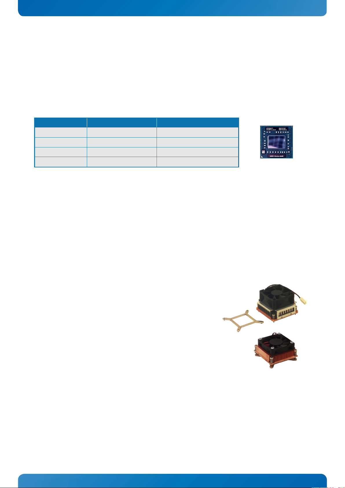
1 Introduction
This manual describes the KTA75/Flex board made by KONTRON Technology A/S. The board will also be
denoted KTA75 within this Users Guide.
The KTA75 is designed to support the below listed APU variants (uPGA 722pin processors) and AMD A75
Fusion Controller Hub (FCH) A75 on a Flex form factor.
APU variants AMD PN Processor data
R-464L RE464LDEC44HJE 2.3 GHz – Quad Core – 35W
R-460H RE460HDEC44HJE 1.9 GHz – Quad Core – 35W
R-272F RE272FDEC23HJE 2.7 GHz – Dual Core – 35W
R-268D RE268DDEC23HJE 2.5 GHz – Dual Core – 35W
See the chapter System Specifications for more specific details.The 4 versions have the same type of active
CPU cooler (the cooler is by default not premounted, but can be ordered with this obtion).
Use of this Users Guide implies a basic knowledge of PC-AT hard- and software. This manual is focused on
describing the KTA75 board’s special features and is not intended to be a standard PC-AT textbook.
New users are recommended to study the Installation Procedure stated in the following chapter before
switching-on the power.
All configuration and setup of the CPU board is either done automatically or manually by the user via the
BIOS setup menus. Only exceptions are the Clear CMOS jumper and the Always On jumper.
Note: Sufficient cooling must be applied to the CPU in order to remove the effect as listed in above table
(Thermal Guideline). The sufficient cooling is also depending on the maximum (worst-case) ambient
operating temperature and the actual load of processor.
The Kontron PN 1044-9447 is “Active Cooler for KTQM67/KTQM77”
capable of being used for processors (fully loaded) having Thermal
Guideline up to 45W @ 60ºC ambient temperature. MTBF is 70.000
hours @ 40ºC.
The Kontron PN 1052-6345 “Cooler Active KTQM67 35W 33mm
longlife” is capable of being used for processors (fully loaded) having
Thermal Guideline up to 35W @ 60ºC ambient temperature. It support
1U and has long life (MTBF is 200.000 hours @ 60ºC).
Latest revision of this manual, datasheet, BIOS, drivers, BSP’s (Board Support Packages), Mechanical
drawings (2D and 3D) can be downloaded from here:
http://kontron.com/products/boards+and+mezzanines/embedded+motherboards/miniitx+motherboards
/kta70mmitx.html
Page 9
KTD-N0861-B Page 1 Installation
KTA75/Flex Users Guide
KTA70M/mITX Users Guide
Warning: Turn off PSU (Power Supply Unit) befor configuring the board and do not hot plug
power supply, otherwise components (RAM, LAN cards etc.) might get damaged.
!
!
Warning: When mounting the board to chassis etc. please notice that the board contains
Note:
Mark
Lock
Make sure the lock is in the
position.
2 Installation Procedure
2.1 Installing the Board
To get the board running, follow these steps. If the board shipped from KONTRON has already components
like CPU and RAM mounted, then relevant steps below can be skipped.
1. Turn off the PSU (Power Supply Unit)
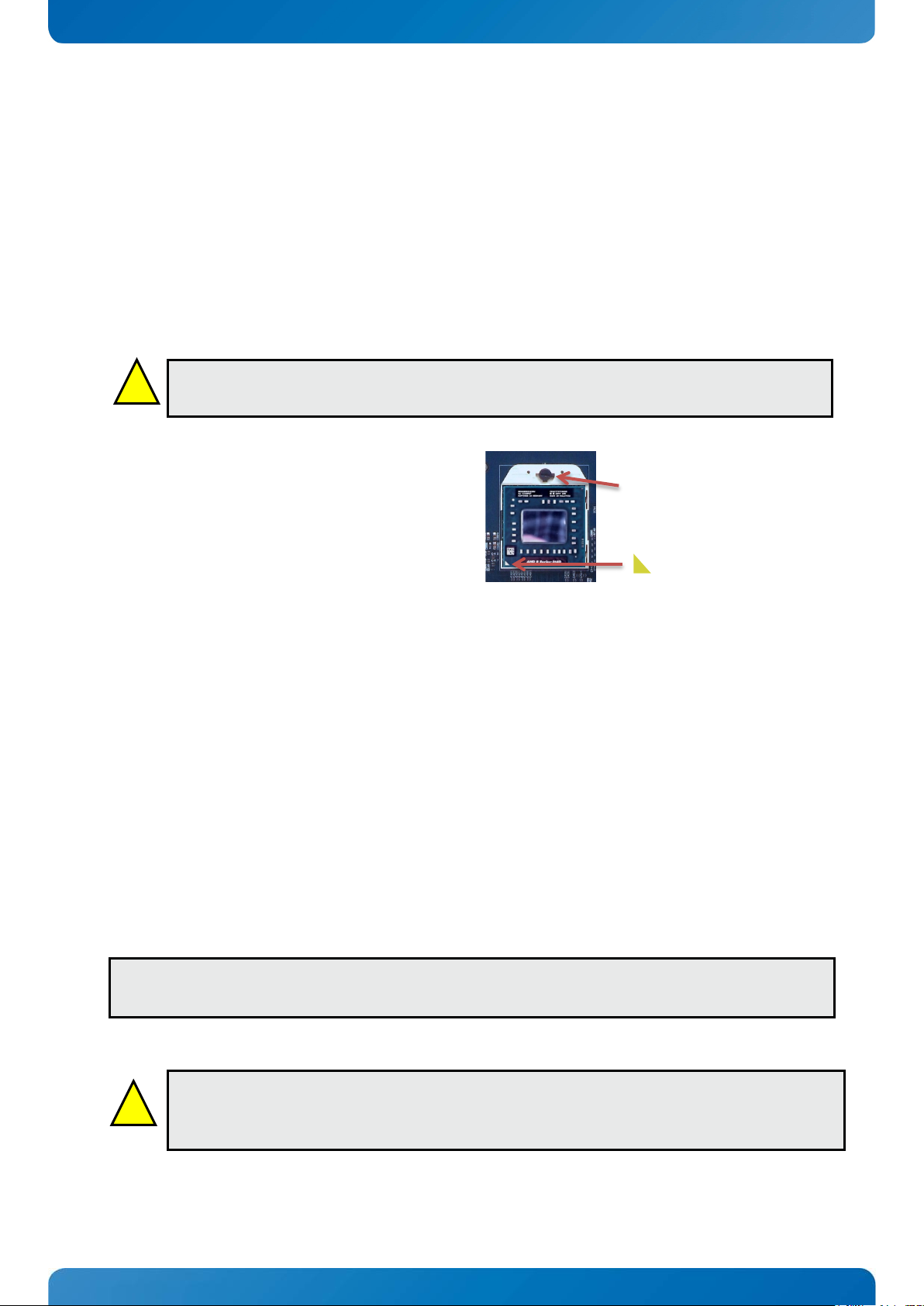
2. Install the CPU into the socket
Insert the CPU, pay attention to the mark.
By use of suitable screwdriver turn the lock to the
locked position.
3. Insert the DDR3 DIMM 240pin module(s)
Be careful to push it in the slot(s) before locking the tabs.
4. Connecting Interfaces and PSU
Insert all external cables for hard disk, keyboard etc. A display/monitor must be connected in order to
be able to change BIOS settings. Connect a standard ATX/BTX PSU to the board by the inserting power
cables into 24-pin ATX and the 4-pin ATX+12V PWR plugs connectors.
5. Power Button
Turn on mains power to the PSU. If board doesn’t boot, then PWRBTN_IN must be toggled; this is done by
shorting pins 16 (PWRBTN_IN) and pin 18 (GND) on the FRONTPNL connector (see Connector
description), by use of a “normally open” switch etc.
6. BIOS Setup
Enter the BIOS setup by pressing the <Del> key during boot up. Enter Exit Menu and Load Optimal
Defaults. Refer to the “BIOS Configuration / Setup“ section of this manual for details on BIOS setup.
7. Mounting the board to chassis
To clear all BIOS settings, including Password protection, activate “Clear CMOS” Jumper for ⋲10
sec (without power connected).
components on both sides of the PCB which can easily be damaged if board is handled without
reasonable care. A damaged component can result in malfunction or no function at all.
unlocked
(Shown in unlocked position)
When fixing the Motherboard on a chassis it is recommended using screws with integrated washer and a
diameter of ⋲7mm. Do not use washers with teeth, as they can damage the PCB and cause short circuits.
Page 10
KTD-N0861-B Page 2 Installation
KTA75/Flex Users Guide
KTA70M/mITX Users Guide
Hersteller empfohlenen gleichwertigen Typ.
Eksplosionsfare ved fejlagtig
Brukte batterier kasseres i
When an interface or connector has a VCC (or other power) pin which is directly connected to a power plane
• That the enclosure of the peripheral device fulfils the fire protecting requirements of IEC60950.
2.2 Requirements IEC60950
Take care when designing chassis interface connectors in order to fulfil the IEC60950 standard.
like the VCC plane:
To protect the external power lines of the peripheral devices the customer has to ensure:
• Wires have suitable rating to withstand the maximum available power.
Lithium battery precautions
CAUTION!
Danger of explosion if battery is incorrectly re- placed.
Replace only with same or equivalent type recommended
by manufacturer. Dispose of used batteries according to
the manufacturer’s instruc- tions.
ATTENTION!
Risque d'explosion avec l'échange inadéquat de la
batterie. Remplacement seulement par le même ou un
type équivalent recommandé par le producteur.
L'évacuation des batteries usagées conformément à des
indications du fabricant.
ADVARSEL!
Lithiumbatteri –
håndtering. Udskiftning må kun ske med batteri af
samme fabrikat og type. Levér det brugte batteri tilbage
til leverandøren.
VARNING!
Explosionsfara vid felaktigt batteribyte. Använd samma
batterityp eller en ekvivalent typ som rekommenderas av
apparattillverkaren. Kassera använt batteri enligt
fabrikantens instruktion.
VORSICHT!
Explosionsgefahr bei unsachgemäßem Austausch der
Batterie. Ersatz nur durch den selben oder einen vom
Entsorgung gebrauchter Batterien nach Anga- ben des
Herstellers.
PRECAUCION!
Peligro de explosión si la batería se sustituye
incorrectamente. Sustituya solamente por el mismo o
tipo equivalente recomendado por el fabricante.
Disponga las baterías usadas según las instrucciones
del fabricante.
ADVARSEL!
Eksplosjonsfare ved feilaktig skifte av batteri. Benytt
samme batteritype eller en tilsvarende type anbefalt av
apparatfabrikanten.
henhold til fabrikantens instruksjoner.
VAROITUS!
Paristo voi räjähtää, jos se on virheellisesti asennettu.
Vaihda paristo ainoastaan lalteval- mistajan
suosittelemaan tyyppiln. Hävitä käytetty paristo
valmistajan ohjeiden mukaisesti.
Page 11
KTD-N0861-B Page 3 System Specification
KTA75/Flex Users Guide
KTA70M/mITX Users Guide
Form factor
Flex: 190,5 x 228,6 mm / 7,5 x 9,0”
Processor
AMD eTrinity FP2 processor:
Companion
AMD A75 (Hudson)Fusion Controller Hub
3 System Specifications
3.1 Component main data
The table below summarizes the features of the KTA75/Flex embedded motherboards.
• Quad-Core 2.3 GHZ with R-464L APU 35W
• Quad Core 1.9 GHz with R-460H APU 35W
• Dual Core 2.7 GHz with R-272F APU 35W
• Dual Core 2.5 GHz with R-268D APU 35W
• Compatible with Existing 32-Bit x86 and 64-bit AMD64 Code Base
• AMD64 64-bit ISA
• High Performance Floating-Point Unit
• SSE 4.1 & 4.2, AVX 1.0 &1.1, AES, XOP, FMA4
• Secure advanced Virtualization Features
• 64-bit DDR3 SDRAM Controller (1333MT/s,666MHz): PC3-10600 /
(1600MT/s,800MHz): PC3-12800
• Compliant with JEDEC DDR3 1.5V and LV-DDR3 1.35V/1.25V SDRAM specification.
Note:LV-DDR3 modules not validated
• PCIe® Technology
• Integrated Memory Controller
• Integrated Graphics AMD Radeon™ HD 7000G Series graphics.
• Dedicated graphics memory controller
• 2D Acceleration Features
• Open GL 4.2 & 2.0
• DirectX® 11 compliant 3D Acceleration Features
• Adaptive Anti Aliasing, Shader Model 5
• Motion Video Acceleration Features
• Dedicated hardware (UVD 3) for H.264
• VC-1, DivX and MPEG2 decode
• HDCP (High-bandwidth Digital Content Protection) supported on DisplayPort.
• Display Port 1.2
• Support DVI/HDMI via passive adapter.
Device
• Unified Media Interface (UMI) (5.0 GT/s)
• PCI Express® 2.0 Controller
• PCI Host Bus Controller
• USB Controllers with up to 14 USB ports
• SMBus Controller
• SATA Controller with RAID 0,1,10 support
• High Definition Audio
• Real Time Clock (RTC)
• Integrated Clock controller
• ACPI 3.0 compliant
Page 12
KTD-N0861-B Page 4 System Specification
KTA75/Flex Users Guide
KTA70M/mITX Users Guide
Memory
Memory controller is integrated in the AMD eTrinity FS1r2 uPGA 722pin processor.
Flash (BIOS)
32Mbit SPI Flash for dual System BIOS.
Security
Intel® Integrated TPM 1.2 support
IT8516E
KT Feature Connector.
Audio Codec
Audio, 7.1 Channel High Definition Audio Codec using the VIA VT1708S codec
Seriel ATA
6x SATA port J9 – J13 & J39, SATA 3.0
Frontpanel
2xUSB, HDD-LED, SYSRST#, SUSLED, PWRBTN#, AUDIO Line/MIC output.
PCI
2x PCI slots (PCI Local Bus Specification revision 2.3 32bit/33MHz)
PCIe
1x PCI Express x16 Slot
DisplayPort
3x DisplayPort connector ( in REAR-IO area)
LVDS
Optionally Add-On card (TBD)
Audio Jack
3x Audiojacks stack J40 (in REAR-IO area)
Audio
Audio Pin header J41
Features are:
• Compliant with JEDEC DDR3 1.5V and (LV-DDR3 1.35V / 1.25 SDRAM, not verified)
specifications
• Supports DDR3 UDIMM 240pin Using up to 8GB DRAM technology
• DDR3 1333/1600MT/s (PC3-10600/PC3-12800)
• From 1GB to 2x 8GB maximum (16GB in total)
Notes: Less than 4GB displayed in System Properties using 32bit OS
(Shared Video Memory/PCI resources is subtracted)
ECC not supported
Infineon TPM SLB9635TT1.2 (FW 3.17)
Embedded
Controller
15 Multiplexed (GPIO, DAC, ADC, PWM & TIMER)
Possible 152 GPIO expansion.
Software Watchdog.
1x mSATA J39 (mechanically sharing space with mPCIe slot J38), SATA 3.0
• RAID 0,1,10 support
1x PCI Express x4 Slot (in mechanically x16 slot)
1x mPCIe Slot J38
1x mPCIe/mSATA J43 (mechanically sharing between mSATA and mPCIe). The mSATA
interface will be selected when a mSATA card are inserted into the mPCIe socket (J43)
DP1 J44
DP2 J3
DP0 J4
Optionally Add-On card with 1x DisplayPort
Blue Line-In
Green Speaker
Pink Mic
Line-out
Line-in
Surround output: SIDE, LFE, CEN, BACK and FRONT
Microphone: MIC1
SPDIF-OUT (electrical Interface only)
Page 13
KTD-N0861-B Page 5 System Specification
KTA75/Flex Users Guide
KTA70M/mITX Users Guide
LAN
Two RJ45 connectors J8 (in REAR-IO area)
USB
14x USB ports (10x USB2.0 & 4x USB2.0/USB3.0):
Serial port
2x RS232 pin header (+12V, -12V supply generated by driver circuit)
LPC
LPC connector J29
FAN
CPUFAN 4 pin row J25 12V PWM
PS2 Kbd/Mse
1x 6 Pin row Keyboard / Mouse PS2 cable kit interface J27
Power Plug
ATX12V: 1x 4 pole connector J19 (core power) and 1x 24 pole connector J17 ATX/BTX
Battery
Speaker
On-board Speaker Piezo
BIOS
AMI EFI
OS (planned)
Windows 7 (32 and 64bit)
• 2x 10/100/1000Mbits/s LAN (ETH1/ETH2) using Intel® Pearsonville xGB PCI Express
Ethernet controller (WGI211ATSLJXZ).
• PXE Netboot supported.
• Wake On LAN (WOL) supported
2x USB2.0 in Frontpanel Connector J5
2x USB2.0 in USB Internal USB Connector J16
4x USB2.0, USB stack J20 (in REAR-IO area)
2x USB 2.0/USB3.0, Right USB stack J14 ( in REAR-IO area)
2x USB 2.0/USB3.0, left USB stack J15 (in REAR-IO area)
1x USB 2.0 in mPCIe socket J38
1x USB 2.0 in mSATA/mPCIe socket J43
COM1 2x 5 Pin row J23
COM2 2x 5 Pin row J22
SYSFAN 4 pin row J24 12V PWM
Exchangeable 3.0V Lithium battery for on-board Real Time Clock and CMOS RAM.
Manufacturer Panasonic / Part-number CR-2032L/BN, CR2032N/BN or CR-2032L/BE.
Approximate 6 years retention.
Current draw is 4 µA when PSU is disconnected and 0 µA in S0 – S5.
CAUTION: Danger of explosion if the battery is incorrectly replaced. Replace only with the
same or equivalent type recommended by the manufacturer. Dispose of used batteries
according to the manufacturer’s instructions.
On-board speaker (Electromagnetic Sound Generator like Hycom HY-05LF)
SPI Connector J21 (for BIOS Recovery)
Clear CMOS J34
Always On J37
Windows 8 (32 and 64bit)
Windows XP (32 bit)
DOS
Windows Embedded 7
Page 14
KTA75/Flex Users Guide
KTA70M/mITX Users Guide
Environmental
Operating:
KTD-N0861-B Page 6 System Specification
0°C – 60°C operating temperature (forced cooling). It is the customer’s responsibility to
provide sufficient airflow around each of the components to keep them within allowed
temperature range.
10% - 90% relative humidity (non-condensing)
Storage:
-20°C – 70°C; lower limit of storage temperature is defined by specification restriction of
on-board CR2032 battery. Board with battery has been verified for storage temperature
down to -40°C by Kontron.
5% - 95% relative humidity (non-condensing)
Electro Static Discharge (ESD) / Radiated Emissions (EMI):
All Peripheral interfaces intended for connection to external equipment are ESD/ EMI
protected.
EN 61000-4-2:2000 ESD Immunity
EN55022:1998 class B Generic Emission Standard.
Safety:
EN 60950-1: 2006/ A11:2009/ A1:2010/A12:2011
IEC 60950-1(ed.2)
CSA C22.2 No. 60950-1
Product Category: Information Technology Equipment Including Electrical Business
Equipment
Product Category CCN: NWGQ2, NWGQ8
File number: E194252 ( E194252-A21-CB-1)
Theoretical MTBF:
314.614 / 153.436 hours @ 40ºC / 60ºC
Restriction of Hazardous Substances (RoHS):
All boards in the KTA75 family are RoHS/RoHS-II compliant.
Capacitor utilization:
No Tantalum capacitors on board
Only Japanese brand Solid capacitors rated for 100 ºC used on board
Page 15
KTD-N0861-B Page 7 System Specification
KTA75/Flex Users Guide
KTA70M/mITX Users Guide
2x UDIMM DDR3
Dual Channel 1067/1333
eTrinity APU
PCIe x16 (x16slot) Graphics
3x DP (DisplayPort 1.2)
4x USB3.0/USB2.0
10x USB2.0
VIA Audio Codec
1x PCIe x4 (x16 slot)
2x PCI 32bit/33MHz
2x 10/100/Gbe
Intel Pearsonville I211AT
5x SATA3.0, RAID0/1/10
TPM (Infineon)
Embedded
ITE8516
Feature connector:
SPI BIOS Flash
2x Fan (CPU/System)
2x COM (RS232)
6-pin PS/2 Keyboard/Mouse
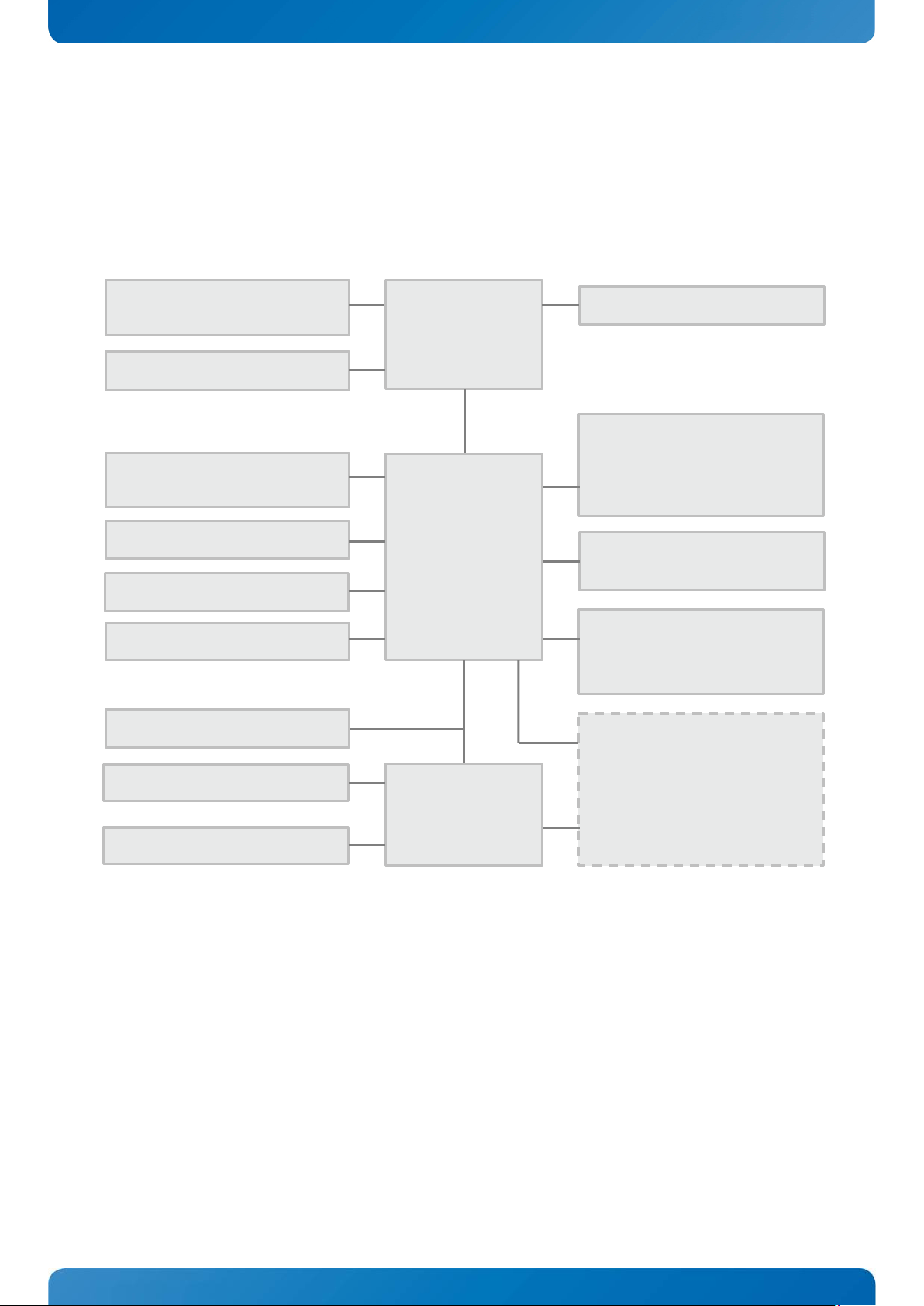
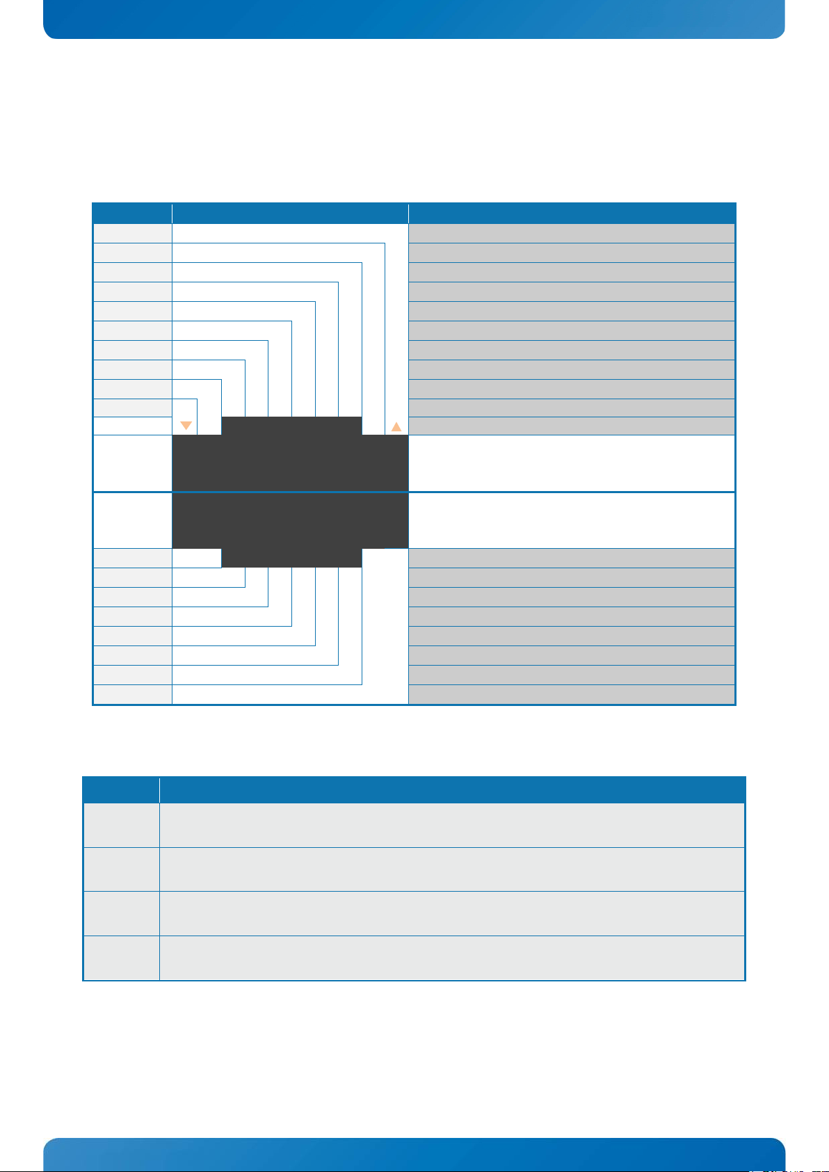
3.2 KTA75/Flex Block Diagram
Processor
722pin uPGA
1x mPCIe w. USB2.0
1x mPCIe/mSATA w. USB2.0
A75
FCH
Controller
1x SATA or mSATA (shared)
(mSATA shared w. mPCIe)
SMBus/I2C
GPIO/DAC/ADC/PWM
GPIO expansion (up to 152)
Intruder
Page 16

KTD-N0861-B Page 8 System Specification
KTA75/Flex Users Guide
KTA70M/mITX Users Guide
ATX supplies
KTA75
PSU
Gnd
Current
Probe
Tektronix TDS5104B
3.3 Power Consumption
On the following pages the power consumption of the KTA75 Board is measured under:
1- DOS, idle, mean
2- Windows 7, Running 3DMARK 2005 & BiT 6, mean
3- S1, mean
4- S3, mean
5- S4, mean
The following items were used in the test setup:
1. Low Power Setup:
Standard system configuration equipped with PCI card, internal graphics, 2x SATA HDD, AMD R-460H
@ 1.9GHz CPU, 1x DIMM (1GB Modules), CRT Monitor, Keyboard & Mouse. 1x 1-4GB USB Stick.
High Power Setup:
Standard system configuration equipped with PCI, PCIex1, PCIex16, miniPCIe WLAN or mSATA HDD, 4x
SATA HDD, AMD R-460H @ 1.9GHz CPU, 2x DIMM (2+2GB Modules), CRT Monitor, Keyboard & Mouse, 4x
4-8GB USB Sticks
2. 12V active cooler (BOX)
3. USB Keyboard/Mouse Genius
4. DELL 2407WFPg
5. 3.5” HDD WD
6. ATX Eurocase 450W
7. Tektronix TDS5104B
8. Tektronix TCPA300
9. Tektronix TCP312
10. Fluke 289
11. ATX Switcher
Note: The Power consumption of Monitor and HDDs is not included.
Warning: Hot Plugging power supply is not supported. Hot plugging might damage the board.
Page 17
KTD-N0861-B Page 9 System Specification
KTA75/Flex Users Guide
KTA70M/mITX Users Guide
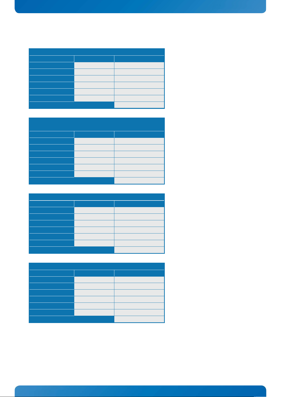
DOS Idle, Mean, No external load
Supply
Current draw
Power consumption
+12V
0.2545A
3.054W
+12V P4
1.4245A
17.094W
+5V
0.6717A
3.3585W
+3V3
0.6496A
2.14368W
-12V
32.17mA
0.38604W
5VSB
0.5mA
0.0025W
Total
26.0387W
Windows 7, mean
3DMARK2005 ( first scene ) & BiT 6
Supply
Current draw
Power consumption
+12V
0.2545A
3.054W
+12V P4
1.8234A
21.8808W
+5V
0.8842A
4.421W
+3V3
0.4789A
1.58037W
-12V
32.12mA
0.38544W
5VSB
0.5mA
0.0025W
Total
31.3241W
S3 Mode, Mean, No external load
Supply
Current draw
Power consumption
+12V
0
0W
+12V P4
0
0W
+5V
0
0W
+3V3
0
0W
-12V
0
0W
5VSB
114.11mA
0.57055W
Total
0.57055W
S4 Mode, Mean, No external load
Supply
Current draw
Power consumption
+12V
0
0W
+12V P4
0
0W
+5V
0
0W
+3V3
0
0W
-12V
0
0W
5VSB
96.52mA
0.4826W
Total
0.4826W
Low Power Setup results:
Page 18
KTD-N0861-B Page 10 System Specification
KTA75/Flex Users Guide
KTA70M/mITX Users Guide
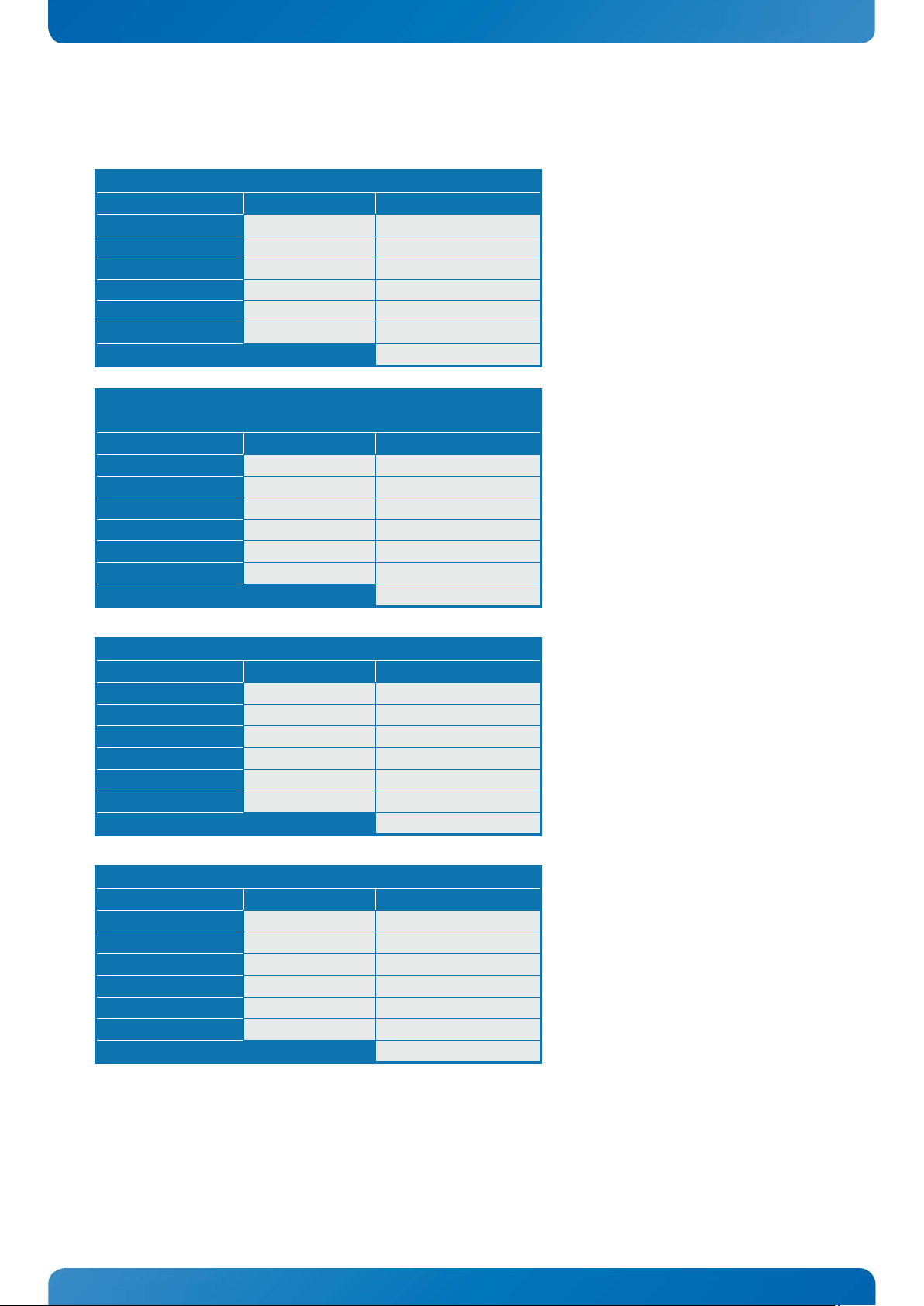
DOS Idle, Mean, No external load
Supply
Current draw
Power consumption
+12V
0.6898A
8.2776W
+12V P4
1.5452A
18.5424W
+5V
1.0571A
5.2855W
+3V3
1.1882A
3.92106W
-12V
32.23mA
0.38676W
5VSB
0.5mA
0.0025W
Total
36.41582W
Windows 7, mean
3DMARK2005 ( first scene ) & BiT 6
Supply
Current draw
Power consumption
+12V
0.6905A
8.286W
+12V P4
2.0547A
24.6564W
+5V
1.4275A
7.1375W
+3V3
1.1967A
3.94911W
-12V
32.43mA
0.38916W
5VSB
0.5mA
0.0025W
Total
44.42067W
S3 Mode, Mean, No external load
Supply
Current draw
Power consumption
+12V
0
0W
+12V P4
0
0W
+5V
0
0W
+3V3
0
0W
-12V
0
0W
5VSB
265.73mA
1.32865W
Total
1.32865W
S4 Mode, Mean, No external load
Supply
Current draw
Power consumption
+12V
0
0W
+12V P4
0
0W
+5V
0
0W
+3V3
0
0W
-12V
0
0W
5VSB
256.37mA
1.28185W
Total
1.28185W
High Power Setup results:
Page 19

KTD-N0861-B Page 11 System Specification
KTA75/Flex Users Guide
KTA70M/mITX Users Guide
USB #
USB standard
Connector location
HCI
Note
USB0
USB1
USB2.0 /USB1.1
Frontpanel (J5)
OHCI1/EHCI1
USB2
USB2.0 /USB1.1
mPCIe (J38)
OHCI1/EHCI1
No over current
detection
USB3
USB2.0 /USB1.1
mSATA/mPCIe (J43)
OHCI1/EHCI1
No over current
detection
USB4
USB2.0 /USB1.1
Pin row (J16)
OHCI1/EHCI1
USB5
USB2.0 /USB1.1
Pin row (J16)
OHCI2/EHCI2
USB6
USB9
USB2.0 /USB1.1
USB quad stack (J20)
OHCI2/EHCI2
USB10
USB11
USB3.0/USB2.0/USB1.1
USB3.0 dual stack (J15)
Left - Rear IO
xHCI1
USB12
USB13
USB3.0/USB2.0/USB1.1
USB3.0 dual stack (J14)
Right - Rear IO
xHCI2
3.4 USB ports overview
The KTA75 board contains two pairs of EHCI (Enhanced Host Controller Interface) and OHCI (Open Host
Controller Interface) in order to support up to 10 USB1.1/USB2.0 devices and further more two xHCI
(Extensible Host Controller Interface) to support up to 4 USB3.0 devices.
The OHCI controllers support USB1.1, Full-Speed (12Mbps) and Low-Speed (1.5Mbps).
The EHCI controllers support USB2.0, High-Speed (480Mbps).
The xHCI controllers support USB3.0, USB2.0 and USB 1.1, Super-Speed (5.0Gbps), High-Speed
(480Mbps), Full-Speed (12Mbps) and Low-Speed (1.5Mbps)
Legacy Keyboard/Mouse and wakeup from sleep states are supported. Over-current detection on all USB
ports except USB2.
USB7
USB8
Rear IO
Notes: In order to meet the requirements of USB standard, the 5V input supply must be at least 5.00V.
The contacts for USB devices are protected and suitable to supply USB devices with a maximum input current of
1000mA.
Do not supply external USB devices with higher power dissipation through these pinsTo protect the external power
lines of peripheral devices make sure that
- the wires have the right diameter to withstand the maximum available current.
- to enclosure of the peripheral device fulfills the fire-protecting conditions of IEC/EN 60950.
Page 20
KTD-N0861-B Page 12 System Specification
KTA75/Flex Users Guide
KTA70M/mITX Users Guide
For USB2.0 cabling it is required to use only HiSpeed USB cable, specified in USB2.0 standard:
For USB3.0 cabling it is required to use only HiSpeed USB cable, specified in USB3.0 standard:
Page 21
KTD-N0861-B Page 13 Connectors Location
KTA75/Flex Users Guide
KTA70M/mITX Users Guide
COM1 J23
COM2 J22
USB4/5 J16
SysFan J24
Power J19
ATX-core power
ClearCMOS J34
Frontpanel J5
CPUFan J25
SATA4 SATA2 SATA0
SATA3 SATA1
SPI J21
PCIex16 J7
PCIex4 J6
(x16 slot)
KBD/MSE J27
Feature J26
UDIMM J1
mPCIe J38
Audio J41
NC J36
AlwaysOn J37
UDIMM J2
LPC J29
USB12 J14
LineIn
DP1 J44
USB10 J15
ETH1
USB6
J20
PCI 32b J18
PCI 32b J28
mSATA/mPCIe J43
Power J17
Note: SATA5 and mSATA (J43) is shared.
4 Connectors Locations
4.1 KTA75/Flex Topview
ATX-BTX
SATA5
(x16 slot)
ETH2
J8
USB7
USB8
USB9
USB13 J14
DP0 J4
USB11 J15
DP2 J3
LineOut
Mic
J40
Page 22

KTD-N0861-B Page 14 Connector Signal Definition
KTA75/Flex Users Guide
KTA70M/mITX Users Guide
The mnemonic name of the signal at the current pin. The notation “#” states that the signal
5 Connector Signal Definitions
The following sections provide pin definitions and detailed description of all onboard connectors.
The connector definitions follow the following notation:
Column Name Description
Pin Shows the pin numbers in the connector.
Signal
is active low.
Type AI: Analogue Input
AO: Analogue Output
I: Digital Input
IO: Digital Input / Output
IOD: Input / Open Drain output
O: Digital Output
DSO: Differential Signaling Output with complementary signals on two paired wires
DSI: Differential Signaling Input with complementary signals on two paired wires
DSIO: Differential Signaling Input / Output (combined DSO and DSI)
PWR: PoWeR supply or ground reference pins
NC: Pin Not Connected
Additional notations:
-5.0 +5.0V signal voltage level, e.g. I-5.0
-3.3 +3.3V signal voltage level, e.g. O-3.3
-1.8 +1.8V signal voltage level, e.g. IO-1.8
Ioh/Iol Ioh: Typical current in mA flowing out of an output pin through a grounded load while the
output voltage has high level.
Iol: Typical current in mA flowing into an output pin from a VCC connected load while the
output voltage has low level.
The abbreviation tbd is used for specifications which are not available yet or which are not sufficiently
specified by the component vendors.
Page 23

KTD-N0861-B Page 15 Rear IO Connectors
KTA75/Flex Users Guide
KTA70M/mITX Users Guide
19 17 15 13 11 9 7 5 3 1
20 18 16 14 12 10 8 6 4 2
1
Lane 0 (p)
LVDS
2
GND
PWR
3
Lane 0 (n)
LVDS
4 Lane 1 (p)
LVDS
5
GND
PWR
6
Lane 1 (n)
LVDS
7
Lane 2 (p)
LVDS
8
GND
PWR
9
Lane 2 (n)
LVDS
10
Lane 3 (p)
LVDS
11
GND
PWR
12
Lane 3 (n)
LVDS
Internally pull down (1Mohm).
DDC channel on pin 15/17, If HDMI adapter used (3.3V)
14
Config2
(Not used)
O
Internally connected to GND
Aux Channel (+)
or DDC Clk
AUX (+) channel used by DP
DDC Clk used by HDMI
16
GND
PWR
Aux Channel (-)
or DDC Data
AUX (-) channel used by DP
DDC Data used by HDMI
18
Hot Plug
I Internally pull down (100Kohm).
19
Return
PWR
Same as GND
20
3.3V
PWR
Fused by 1.5A resetable PTC fuse, common for DP0 and DP1
6 Rear IO Connectors
6.1 DisplayPort (DP0/DP1/DP2)(J4/J43/J3)
The DP (DisplayPort) connectors are based on standard DP type Foxconn 3VD11203-H7AB-4H or similar.
Pin Signal Description Type Note
13 Config1
15 Aux Ch (p)
17 Aux Ch (n)
Note: To protect the external power lines of peripheral devices make sure that
- the wires have the right diameter to withstand the maximum available current.
- to enclosure of the peripheral device fulfills the fire-protecting conditions of IEC/EN 60950.
Aux or DDC
selection
I
Aux channel on pin 15/17 selected as default (when NC)
Page 24
KTD-N0861-B Page 16 Rear IO Connectors
KTA75/Flex Users Guide
KTA70M/mITX Users Guide
The 3 DisplayPorts (DP0, DP1 and DP2) can be used in a 3 independent display configuration. By use of DP
Adapter Converters it is possible to implement a mix of DP, VGA, HDMI and DVI-D outputs and still support 3
independent displays configuration.
Available DP adapters:
DP to VGA DP to HDMI DP to DVI-D
PN 1045-5779 PN 1045-5781 PN 1045-5780
DP Extention Cable:
In order to prevent mechanical conflicts the above DP adapters can be connected to DP#0, DP#1 and DP#2
via the 1051-7619 Cable DP Extender cable 200mm.
The DP to VGA adapter is an “active” converter, meaning that seen from the graphics controller it looks like
a DP. The HDMI and DVI converters are passive converters, meaning that they inform the graphics
controller about its type and the graphics controller then replace the DP signals with TMDS signals (used in
HDMI and DVI).
The HDMI interface supports the HDMI 1.4a specification including audio codec. Limitations to the
resolution apply: 2048x1536 (VGA), 1920x1200 (HDMI and DVI).
Four independent (simultaneously) displays (without using PCIe Graphics cards) is a possible configuration
under the following conditions:
1. A DP-PCIe passive card or DP-DVI passive card must be used in the outermost PCIe slot.
2. All DP must be converted to DVI-D or HDMI via passive adapters like above adapters.
3. Two of the panels must have the same timing (as if two panels are of the exact same type).
Page 25
KTD-N0861-B Page 17 Rear IO Connectors
KTA75/Flex Users Guide
KTA70M/mITX Users Guide
Note
Type
Signal
PIN
Signal
Type
Note
DSIO-3.3
USB10-
USB10+
DSIO-3.3
1
PWR
5V/SB5V
1 2 3 4 GND
PWR
DSIO-3.3
RX10-
5 6 7 8 9
TX10+
DSIO-3.3
DSIO-3.3
RX10+
TX10-
DSIO-3.3
PWR
GND
DSIO-3.3
USB11-
USB11+
DSIO-3.3
1
PWR
5V/SB5V
1 2 3 4 GND
PWR
DSIO-3.3
RX11-
5 6 7 8 9
TX11+
DSIO-3.3
DSIO-3.3
RX11+
TX11-
DSIO-3.3
PWR
GND
Note
Type
Signal
PIN
Signal
Type
Note
DSIO-3.3
USB12-
USB12+
DSIO-3.3
1
PWR
5V/SB5V
1 2 3 4 GND
PWR
DSIO-3.3
RX12-
5 6 7 8 9
TX12+
DSIO-3.3
DSIO-3.3
RX12+
TX12-
DSIO-3.3
PWR
GND
DSIO-3.3
USB13-
USB13+
DSIO-3.3
1
PWR
5V/SB5V
1 2 3 4 GND
PWR
DSIO-3.3
RX13-
5 6 7 8 9
TX13+
DSIO-3.3
IO
RX13+
TX13-
DSIO-3.3
PWR
GND
6.2 USB3.0 Connectors (USB10/USB11/USB12/USB13)(J15/J15/J14/J14)
The USB3.0 connectors are based on standard USB3.0 connectors type Lotes ABA-USB-104-K01 or similar.
Thease 4 USB3.0 ports are controlled by the xHCI controllers supporting USB3.0, USB2.0 and USB 1.1,
Super-Speed (5.0Gbps), High-Speed (480Mbps), Full-Speed (12Mbps) and Low-Speed (1.5Mbps)
USB Ports 10 and 11 (mounted on top of the DP#2 port):
Signal Description
USB10+ USB10-
RX10+ RX10-
TX10+ TX10-
USB11+ USB11-
RX11+ RX11-
TX11+ TX11-
5V/SB5V
USB Ports 12 and 13 (mounted on top of the DP#0 port):
Differential pair works as Data/Address/Command Bus.
5V supply for external device. SB5V is supplied during powerdown to allow wakeup on
device activity. Protected by current limited power distribution switch,1A for each port.
Page 26
KTD-N0861-B Page 18 Rear IO Connectors
KTA75/Flex Users Guide
KTA70M/mITX Users Guide
Signal Description
USB12+ USB12-
RX12+ RX12-
TX12+ TX12-
USB13+ USB13-
RX13+ RX13-
TX13+ TX13-
Differential pair works as Data/Address/Command Bus.
5V/SB5V
5V supply for external device. SB5V is supplied during powerdown to allow wakeup on
device activity. Protected by current limited power distribution switch,1A for each port.
Notes: In order to meet the requirements of USB standard, the 5V input supply must be at least 5.00V.
The contacts for USB devices are protected and suitable to supply USB devices with a maximum input current of
1000mA.
Do not supply external USB devices with higher power dissipation through these pinsTo protect the external power
lines of peripheral devices make sure that
- the wires have the right diameter to withstand the maximum available current.
- to enclosure of the peripheral device fulfills the fire-protecting conditions of IEC/EN 60950.
Page 27
KTD-N0861-B Page 19 Rear IO Connectors
KTA75/Flex Users Guide
KTA70M/mITX Users Guide
Signal
PIN
Note
LED1
LED Lights when ETH1 Link, Flashing when activity
MDI0+
MDI0-
MDI1+
MDI2+
MDI2-
MDI1-
MDI3+
MDI3-
LED2
LED Lights when ETH2 Link, Flashing when activity
ETH1
8 7 6 5 4 3 2 1
ETH2
1 2 3 4 5 6 7 8
MDI0+
MDI0-
MDI1+
MDI2+
MDI2-
MDI1-
MDI3+
MDI3-
6.3 Ethernet Connectors (ETH1/ETH2) (J8)
The KTA75 supports two 10/100/1000Mb Ethernet RJ45 connetors in a stacked dual LAN connector, type
Ude RMT-123AGF1F or sililar. Both ports are driven by Intel® Pearsonville WGI211AT PCI Express controller.
Ethernet connector 1 (ETH1) is mounted above Ethernet connector 2 (ETH2).
In order to achieve the specified performance of the Ethernet port, Category 5 twisted pair cables must be
used with 10/100MB and Category 5E, 6 or 6E with 1Gb LAN networks.
Signal Description
MDI[0]+ /
MDI[0]-
MDI[1]+ /
MDI[1]-
MDI[2]+ /
MDI[2]-
MDI[3]+ /
MDI[3]-
Note: MDI = Media Dependent Interface.
MDI mode: first pair in 1000Base-T (i.e. the BI_DA+/- pair), transmit pair in 10/100Base-T.
MDI crossover mode: acts as the BI_DB+/- pair, receive pair in 10/100Base-TX.
MDI mode: second pair in 1000Base-T (i.e. the BI_DB+/- pair), receive pair in 10/100Base-T.
MDI crossover mode: acts as the BI_DA+/- pair, transmit pair in 10/100Base-T.
MDI mode: third pair in 1000Base-T (i.e. the BI_DC+/- pair).
MDI crossover mode: acts as the BI_DD+/- pair.
MDI mode: fourth pair in 1000Base-T (i.e. the BI_DD+/- pair).
MDI crossover mode: acts as the BI_DC+/- pair.
Page 28

KTD-N0861-B Page 20 Rear IO Connectors
KTA75/Flex Users Guide
KTA70M/mITX Users Guide
Note
Type
Signal
PIN
Signal
Type
Note
PWR
5V/SB5V
1 2 3 4 GND
PWR
DSIO-3.3
USB6-
USB6+
DSIO-3.3
PWR
5V/SB5V
1 2 3 4 GND
PWR
DSIO-3.3
USB7-
USB7+
DSIO-3.3
PWR
5V/SB5V
1 2 3 4 GND
PWR
DSIO-3.3
USB8-
USB8+
DSIO-3.3
PWR
5V/SB5V
1 2 3 4 GND
PWR
DSIO-3.3
USB9-
USB9+
DSIO-3.3
6.4 USB x4 Stack Connector (USB6/USB7/USB8/USB9) (J20)
USB Ports 6, 7, 8 and 9 are mounted in a single stack in the IO Area type Foxconn UB11123-Q8DF-4F or
similar. The USB ports are controlled by a single set of OHCI and EHCI controllers (also shared by USB5).
The OHCI controllers support USB1.1, Full-Speed (12Mbps) and Low-Speed (1.5Mbps).
The EHCI controllers support USB2.0, High-Speed (480Mbps).
Signal Description
USB6+ USB6USB7+ USB7-
USB8+ USB8-
Differential pair works as Data/Address/Command Bus.
USB9+ USB9-
5V/SB5V
5V supply for external devices. SB5V is supplied during powerdown to allow wakeup on
USB device activity. Protected by individual resettable 1A fuse.
Notes: In order to meet the requirements of USB standard, the 5V input supply must be at least 5.00V.
The contacts for USB devices are protected and suitable to supply USB devices with a maximum input current of
1000mA.
Do not supply external USB devices with higher power dissipation through these pinsTo protect the external power
lines of peripheral devices make sure that
- the wires have the right diameter to withstand the maximum available current.
- to enclosure of the peripheral device fulfills the fire-protecting conditions of IEC/EN 60950.
Page 29

KTD-N0861-B Page 21 Rear IO Connectors
KTA75/Flex Users Guide
KTA70M/mITX Users Guide
Signal
Type
Note
TIP LINE1-L
IA
RING LINE1-R
IA
SLEEVE GND
PWR
TIP
FRONT-OUT-L
OA
SLEEVE GND
PWR
TIP MIC1-L
IA
RING MIC1-R
IA
SLEEVE GND
PWR
6.5 Audio Interface (J40)
The on-board Audio circuit, based on Via VT1708S, implements 7.1+2 Channel High Definition Audio with
UAA (Universal Audio Architecture), featuring five 24-bit stereo DACs and three 20-bit stereo ADCs. The
Following Audio connector is available in IO Area.
Audio Speakers, Line-in and Microphone are available in the stacked audiojack connector type Lotes ABAJAK-028-K03
RING FRONT-OUT-R OA
Signal Description Note
FRONT-OUT-L Front Speakers (Speaker Out Left).
FRONT-OUT-R Front Speakers (Speaker Out Right).
MIC1-L Microphone 1 - Left Shared with Audio Header
MIC1-R
LINE1-L Line 1 signal - Left
LINE1-R Line 1 signal - Right
Microphone 1 - Right Shared with Audio Header
Shared with Audio Header
Shared with Audio Header
Page 30

KTD-N0861-B Page 22 Pin Connectors
KTA75/Flex Users Guide
KTA70M/mITX Users Guide
Header
Note
Type
Signal
PIN
Signal
Type
Note
PWR
3V3
12
24 GND
PWR
PWR
+12V
11
23 5V
PWR
PWR
+12V
10
22 5V
PWR
PWR
SB5V
9
21 5V
PWR
I P_OK
8
20 -5V
PWR 1
PWR
GND
7
19 GND
PWR
PWR
5V
6
18 GND
PWR
PWR
GND
5
17 GND
PWR
PWR
5V
4
16 PSON#
OC
PWR
GND
3
15 GND
PWR
PWR
3V3
2
14 -12V
PWR
PWR
3V3
1
13 3V3
PWR
P_OK is a power good signal and should be asserted high by the power supply to indicate that
7 Pin Connectors
7.1 24-pin ATX-BTX Power Connector (J17)
The KTA75 boards are designed to be supplied from a standard ATX (or BTX) power supply. Use of BTX supply
is not required for operation, but may be required to drive high-power PCIe cards.
ATX-BTX Power Connector (J17):
Note 1: -5V supply is not used on-board.
See chapter “Power Consumption” regarding input tolerances on 3.3V, 5V, SB5V, +12 and -12V (also refer
to ATX specification version 2.2).
Signal Description
P_OK
the +5VDC and +3.3VDC outputs are above the undervoltage thresholds of the power supply.
When this signal is asserted high, there should be sufficient energy stored by the converter to
guarantee continuous power operation within specification. Conversely, when the output
voltages fall below the undervoltage threshold, or when mains power has been removed for a
time sufficiently long so that power supply operation is no longer guaranteed, P_OK should be
de-asserted to a low state. The recommended electrical and timing characteristics of the P_OK
(PWR_OK) signal are provided in the ATX12V Power SupplyDesign Guide.
It is strongly recommended to use an ATX or BTX supply in order to implement the supervision
of the 5V and 3V3 supplies. These supplies are not supervised on-board.
PS_ON#
Active low open drain signal from the board to the power supply to turn on the power supply
outputs. Signal must be pulled high by the power supply.
Page 31

KTD-N0861-B Page 23 Pin Connectors
KTA75/Flex Users Guide
KTA70M/mITX Users Guide
Header
Pin
Signal
Description
1
GND
Ground
2
GND
Ground
3
12V
Power supply +12V
4
12V
Power supply +12V
7.2 4-pin 12V Power Connector (J19)
The KTA75/Flex has an internal power input connector for supplying voltage in the range from +11.4V to
+12.6V. The power connector is a 4 pin 12V ATX connector type Lotes ABA-POW-003-K02 or similar.
Warning: Hot Plugging power supply is not supported. Hot plugging might damage the board.
Note 1: Use of the 4-pin ATX+12V Power Connector is required for operation of all KTA75 board versions.
Notes: To protect the external power lines of peripheral devices make sure that
- the wires have the right diameter to withstand the maximum available current.
- to enclosure of the peripheral device fulfills the fire-protecting conditions of IEC/EN 60950.
Alternatively the DC Power External Connector can be used
Page 32

KTD-N0861-B Page 24 Pin Connectors
KTA75/Flex Users Guide
KTA70M/mITX Users Guide
Note
Type
Signal
PIN
Signal
Type
Note
AO
LFE-OUT
1 2 CEN-OUT
AO
PWR
AAGND
3 4 AAGND
PWR
1
AO
FRONT-OUT-L
5 6 FRONT-OUT-R
AO 1
PWR
AAGND
7 8 AAGND
PWR
AO
REAR-OUT-L
9 10 REAR-OUT-R
AO
AO
SIDE-OUT-L
11
12 SIDE-OUT-R
AO
PWR
AAGND
13
14 AAGND
PWR
1
AI
MIC1-L
15
16 MIC1-R
AI
1
PWR
AAGND
17
18 AAGND
PWR
1 LINE1-L
19
20 LINE1-R
1
NC
NC
21
22 AAGND
PWR
PWR
GND
23
24 NC
NC
O SPDIF-OUT
25
26 GND
PWR
7.3 Audio Header Connector (J41)
The Audio Header connector is a 26 pin connector type Molex 87832-2620 or similar.
Note 1: Shared with Audio Stack connector (in Rear IO area).
Signal Description
FRONT-OUT-L Front Speakers (Speaker Out Left).
FRONT-OUT-R Front Speakers (Speaker Out Right).
REAR-OUT-L
REAR-OUT-R
SIDE-OUT-L
SIDE-OUT-R
CEN-OUT
LFE-OUT Subwoofer Speaker (Low Freq. Effect Out).
NC No connection
MIC1 MIC Input 1
LINE1 Line 1 signals
F-SPDIF-OUT S/PDIF Output
AAGND Audio Analogue ground
Available cable kit:
PN 821043 Cable, Audio Open-End (300 mm)
Rear Speakers (Surround Out Left).
Rear Speakers (Surround Out Right).
Side speakers (Surround Out Left)
Side speakers (Surround Out Right)
Center Speaker (Center Out channel).
Page 33

KTD-N0861-B Page 25 Pin Connectors
KTA75/Flex Users Guide
KTA70M/mITX Users Guide
Header
Pin
Signal
Description
Type
1
5V/SB5V
5V (always) protected by separate 1A resettable fuse
PWR
2
5V/SB5V
5V (always) protected by separate 1A resettable fuse
PWR
3
USB4-
Differential pair 4 -
DSIO-3.3
4
USB5-
Differential pair 5 -
DSIO-3.3
5
USB4+
Differential pair 4 +
DSIO-3.3
6
USB4+
Differential pair 5 +
DSIO-3.3
7
GND
Ground
PWR
8
GND
Ground
PWR -
(pin not mounted -Used for keying)
10
KEY NC
7.4 USB4/5 Connector (J16)
USB Ports 4 and 5 are available via Pin Row connector type Foxconn HS1105F-RNP9 or similar.
The USB4 port is controlled by a set of OHCI and EHCI controllers (also shared by USB0/1/2).
The USB5 port is controlled by a set of OHCI and EHCI controllers (also shared by USB6/7/8/9).
The OHCI controllers support USB1.1, Full-Speed (12Mbps) and Low-Speed (1.5Mbps).
The EHCI controllers support USB2.0, High-Speed (480Mbps).
Notes: In order to meet the requirements of USB standard, the 5V input supply must be at least 5.00V.
The contacts for USB devices are protected and suitable to supply USB devices with a maximum input current of
1000mA.
Do not supply external USB devices with higher power dissipation through these pinsTo protect the external power
lines of peripheral devices make sure that
- the wires have the right diameter to withstand the maximum available current.
- to enclosure of the peripheral device fulfills the fire-protecting conditions of IEC/EN 60950.
Available cable kit:
PN 821401 Bracket Dual USB Cable
Page 34

KTD-N0861-B Page 26 Pin Connectors
KTA75/Flex Users Guide
KTA70M/mITX Users Guide
!
Jumper in position
Pin
Jumper in position
1 2 3
Always On
J37
-
Always On
Clear CMOS
J34
Clear CMOS
Normal (Default)
Audio Short circuit test
J36
Front Right
Front Left
Not mounted
J35 - -
7.5 Jumper area (J34, J35, J36, J37)
The KTA75 has a jumper area containing pin connectors 2.54mm pitch, for up to four jumpers, but normally
only one jumper is used (jumper in the J34 pin 2-3 position, as indicated below).
Function J#
Always On: is PT not supported.
(None): Not mounted on final version of board. Only mounted on Early Field Test versions of KTA75.
Clear CMOS: is used to erase all customised BIOS settings located in the CMOS RAM storage. If the board has
a booting problem or is unstabile, then Clearing CMOS by moving the Jumper from default position to the
Clear CMOS position for approx. 10 sec. might solve the problem.
Warning
Audio Short Circuit Test: is only used in manufacturing test. No jumper should be installed.
Don’t leave the Clear CMOS jumper in position 1-2, otherwise if power is
disconnected, the battery will fully deplete within a few weeks.
1-2
2-3
Page 35

KTD-N0861-B Page 27 Pin Connectors
KTA75/Flex Users Guide
KTA70M/mITX Users Guide
Header
Pin
Signal
Description
Type
1
SPI_CLK
SPI clock
O-3.3 2 3.3V
Power +3.3V
PWR
3
SPI_CS#
SPI slave select, active low
O-3.3
4
ADDIN
Disable onboard SPI flash
I-3.3 5 RSVD
Reserved (10k pullup to 3.3V)
PWR 6 N.C.
Not connected
NC
7
SPI_MOSI
SPI master output, Slave Input
IO-3.3
8
ISOLATE#
Disable the SPI interface
I-3.3
9
SPI_MISO
SPI master input, Slave Output
IO-3.3
10
GND
Ground
PWR
3.3V Standby Voltage power line. Normally output power, but when Motherboard is turned
The ISOLATE# input, active low, is normally NC, but must be connected to GND when
loading SPI flash. Power Supply to the Motherboard must be turned off when loading SPI
1
7.6 SPI Connector (J21)
The KTA75 provides one synchronous full duplex SPI (Serial Peripheral Interface) Bus in a 10 pin header
connector. The connector is type Pinrex 512-90-10GBE5 or similar.
Two things should be considered:
1. An onboard SPI
3.3V power connection to the ADDIN signal (e.g. a short circuit jumper between pin 2 and 4).
2. The four SPI
output enable pin. For normal operation this signal should be high.
TM
flash coexists on the same interface lines. You must disable this component with a
TM
lines are protected with an additional bus driver and the ISOLATE# signal controls the
Signal Further description
SB3V3
off then the on-board SPI Flash can be 3.3V power sourced via this pin.
ISOLATE#
flash. The pull up resistor is connected via diode to 5VSB.
Page 36

KTD-N0861-B Page 28 Pin Connectors
KTA75/Flex Users Guide
KTA70M/mITX Users Guide
Note
Ioh/Iol
Type
Signal
PIN
Signal
Type
Ioh/Iol
Note
- I
DCD
1 2 DSR I -
- I
RxD
3 4 RTS O
O
TxD
5 6 CTS I -
O
DTR
7 8 RI I -
- PWR
GND
9 10 5V
PWR - 1
7.7 COM1/COM2 (J23/J22)
Two serial ports provide asynchronous serial communication via RS-232 interfaces. The connector is type
Pinrex 512-90-10GBE5 or similar.
The pinout of Serial ports COM1 and COM2 is as follows:
Note 1: The COM1 and COM4 5V supply is fused with a common 1.1A resettable fuse.
The typical definition of the signals in the COM ports is as follows:
Signal Description
TxD
Transmitted Data, sends data to the communications link. The signal is set to the marking state (12V) on hardware reset when the transmitter is empty or when loop mode operation is initiated.
RxD Received Data, receives data from the communications link.
DTR
Data Terminal Ready, indicates to the modem etc. that the on-board UART is ready to establish a
communication link.
DSR Data Set Ready, indicates that the modem etc. is ready to establish a communications link.
RTS Request To Send, indicates to the modem etc. that the on-board UART is ready to exchange data.
CTS Clear To Send, indicates that the modem or data set is ready to exchange data.
DCD Data Carrier Detect, indicates that the modem or data set has detected the data carrier.
RI Ring Indicator, indicates that the modem has received a ringing signal from the telephone line.
Available cable kit (DB9 adapter cables):
PN 821017 - 100 mm or PN 821016 - 200 mm
Page 37

KTD-N0861-B Page 29 Pin Connectors
KTA75/Flex Users Guide
KTA70M/mITX Users Guide
Pull
U/D
Pull
U/D
- -
PWR
LPC CLK
1 2 GND
- -
PWR
LPC FRAME#
3 KEY
LPC RST#
5 6 +5V
LPC AD3
7 8 LPC AD2
+3V3
9
10
LPC AD1
LPC AD0
11
12
GND
SMB_CLK
13
14
SMB_DATA
SB3V3
15
16
LPC SERIRQ
GND
17
18
CLKRUN#
SUS_STAT#
19
20
NC
7.8 LPC Connector (J29)
The LPC connector is unsupported. The connector is type Foxconn HC11101-P0 or similar.
Note
Ioh/Iol Type Signal PIN Signal Type Ioh/Iol
Note
Page 38

KTD-N0861-B Page 30 Pin Connectors
KTA75/Flex Users Guide
KTA70M/mITX Users Guide
Pull
U/D
Ioh/
Iol
Ioh/
Iol
Pull
U/D
- -
PWR
USB0_5V
1 2 USB1_5V
PWR - -
- - USB0-
3 4 USB1-
- -
- - USB0+
5 6 USB1+
- -
- -
PWR
GND
7 8 GND
PWR - - - -
NC
NC
9 10 LINE2-L
- -
- -
PWR
+5V
11
12 +5V
PWR - -
- 25/25mA
O
SATA_LED#
13
14 SUS_LED
O
7mA -
- -
PWR
GND
15
16 PWRBTN_IN#
I 1K1
4K7 - I
RSTIN#
17
18 GND
PWR - -
- -
PWR
SB3V3
19
20 LINE2-R
- -
- -
PWR
AGND
21
22 AGND
PWR - - - -
AI
MIC2-L
23
24 MIC2-R
AI - -
5V supply for external devices. SB5V is supplied during powerdown to allow wakeup
on USB device activity. Protected by independed resettable 1.1A fuse.
Power Button In. Toggle this signal low to start the ATX / BTX PSU and boot the
Reset Input. When pulled low for a minimum 16ms, the reset process will be initiated.
7.9 Front Panel Connector (J5)
The Front Panel connector is a 24 pin connector type Wieson G2120HT0038-016 or similar.
Note
Signal Description
USB0_5V/USB1_5V
USB0+/USB0- Universal Serial Bus Port 0 Differentials: Bus Data/Address/Command Bus.
USB1+/USB1- Universal Serial Bus Port 1 Differentials: Bus Data/Address/Command Bus.
+5V Maximum load is 1A if using IDC connector or 2A if using crimp terminals .
Type Signal PIN Signal Type
Note
SATA_LED# SATA Activity LED (active low signal). 3V3 output when passive.
SUS_LED Suspend Mode LED (active high signal). Output 3.3V via 470Ω.
PWRBTN_IN#
RSTIN#
LINE2
MIC2
SB3V3
AGND Analogue Ground for Audio
Note: In order to meet the requirements of USB standard, the 5V input supply must be at least 5.00V.
Available cable kit:
board.
The reset process continues even though the Reset Input is kept low.
Line2 is second stereo Line signals
MIC2 is second stereo microphone input.
Standby 3.3V voltage
PN 821042 Cable Front Panel Open-End, 300 mm
Page 39

KTD-N0861-B Page 31 Pin Connectors
KTA75/Flex Users Guide
KTA70M/mITX Users Guide
Header
Pin
Signal
Description
Type
1
PWM
PWM output
O-3.3
2
TACHO
Tacho signal (open drain)
I 3 12V
Power +12V
PWR 4 GND
Ground
PWR
PWM
PWM is output signal used to control the fan speed (only for 4-wire Fans).
Tarcho input signal is used to monitor the rotation speed RPM (Rotation Per Minute).
7.10 CPU/System Fan Connectors (J25, J24)
The CPU Fan connector and the System Fan connector are identical 4 pin type connectors. The type is Tyco
1470947-1 or similar.
Signal Description
Tacho
Prepared for two pulses per turn.
Page 40

KTD-N0861-B Page 32 Pin Connectors
KTA75/Flex Users Guide
KTA70M/mITX Users Guide
Note
Pull U/D
Ioh/Iol
Type
Signal
PIN
Signal
Type
Ioh/Iol
Pull U/D
Note
2
2M/
-
I
CASE_OPEN#
1 2 SMBC
/4mA
10K/
1
- 25/25mA
O
S5#
3 4 SMBD
/4mA
10K/
1
- 25/25mA
O
PWR_OK
5 6 EXT_BAT
PWR - -
4 - O FAN3OUT
7 8 FAN3IN I -
10K/
4
- -
PWR
SB3V3
9 10 SB5V
PWR - -
-
IOT
GPIO0
11
12 GPIO1
IOT -
-
IOT
GPIO2
13
14 GPIO3
IOT - -
IOT
GPIO4
15
16 GPIO5
IOT -
-
IOT
GPIO6
17
18 GPIO7
IOT -
- -
PWR
GND
19
20 GND
PWR - -
- I GPIO8
21
22 GPIO9 I -
3 -
NC
GPIO10
23
24 GPIO11
NC - 3 - I GPIO12
25
26 GPIO13
IOT -
-
IOT
GPIO14
27
28 GPIO15
IOT -
-
IOT
GPIO16
29
30 GPIO17
NC -
3
- -
PWR
GND
31
32 GND
PWR - -
- 8/8mA
O
EGCLK
33
34 EGCS#
O
8/8mA
-
- 8/8mA
EGAD
35
36 TMA0 O
-
PWR
+12V
37
38 GND
PWR - - 4 - O FAN4OUT
39
40 FAN4IN I -
10K/
4
- -
PWR
GND
41
42 GND
PWR - -
- -
PWR
GND
43
44 S3#
O
25/25mA
-
7.11 Feature Connector (J26)
The Feature Connector is a 44 pin connector, 2 mm pitch, type Foxconn HS5422F or similar.
Notes: 1. Pull-up to SB3V3.
2. Pull-up to on-board Battery.
3. Not connected, used for onboard feature.
4. Not supported.
Available cable kit:
PN 1052-5885 Cable, Feature 44pol 1 to1, 300mm
Page 41

KTD-N0861-B Page 33 Pin Connectors
KTA75/Flex Users Guide
KTA70M/mITX Users Guide
CASE OPEN, used to detect if the system case has been opened. This signal’s status is
readable, so it may be used like a GPI when the Intruder switch is not required.
PoWeR OK, signal is high if no power failures are detected. (This is not the same as the
P_OK signal generated by ATX PSU).
(EXTernal BATtery) option for connecting + terminal of an external primary cell battery
terminal connected to GND). The external battery is protected against
charging and can be used with/without the on-board battery installed.
General Purpose Inputs / Output. These Signals may be controlled or monitored through
GPIO10, GPIO11 and GPIO17 are not supported (not connected).
Signal Description
CASE_OPEN# *
SMBC SMBus Clock signal
SMBD SMBus Data signal
S3#
S5#
S3 sleep mode, active low output, optionally used to deactivate external system.
S5 sleep mode, active low output, optionally used to deactivate external system.
PWR_OK
EXT_BAT *
(2.5 - 4.0 V) (–
FAN3OUT Not Supported
FAN3IN Not Supported
FAN4OUT Not Supported
FAN4IN Not Supported
SB3V3 +3.3V StandBy voltage, max. load 1 Amp
SB5V +5V StandBy voltage
GPIO0..17 *
EGCLK *
the use of the KT-API-V2 (Application Programming Interface).
Extend GPIO Clock signal
EGAD * Extend GPIO Address Data signal
EGCS# * Extend GPIO Chip Select signal, active low
TMA0 Timer Output
+12V +12V, max. load 1 Amp.
(*) = Not verified.
Available Temperature Sensor cable kit (for System Fan Temperature Cruise, selected in BIOS):
Based on Maxim DS18B20, Accurate to ±0.5ºC over the range of -10ºC to +85ºC
Feature connector 3.3V (Pin 9), GND (Pin 19) and GPIO16 (Pin 29)
PN1053-4925 Cable Temperature Sensor - 44P, 400 mm
Page 42

KTD-N0861-B Page 34 Pin Connectors
KTA75/Flex Users Guide
KTA70M/mITX Users Guide
GPIO0
DAC0/GPJ0
AO/IOS
GPIO1
DAC1/GPJ1
AO/IOS
GPIO2
DAC2/GPJ2
AO/IOS
GPIO3
DAC3/GPJ3
AO/IOS
GPIO4
PWM2/GPA2
O8/IOS
GPIO5
PWM3/GPA3
O8/IOS
GPIO6
PWM4/GPA4
O8/IOS
GPIO7
PWM5/GPA5
O8/IOS
GPIO8
ADC0/GPI0
AI/IS
GPIO9
ADC1/GPI1
AI/IS
GPIO10
ADC2/GPI2
AI/IS
Reserved, used for System Temperature
GPIO11
ADC3/GPI3
AI/IS
Reserved, used for +12V monitoring
GPIO12
ADC4/WUI28/GPI4
AI/IS/IS
GPIO13
RI1#/WUI0/GPD0
IS/IS/IOS
GPIO14
RI2#/WUI1/GPD1
IS/IS/IOS
GPIO15
TMRI0/WUI2/GPC4
IS/IS/IOS
GPIO16
TMRI1/WUI3/GPC6
IS/IS/IOS
Optionally for Cable Temperature sensor
GPIO17
L80HLAT/BAO/WUI24/GPE0
O4/O4/IS/IOS
Reserved, used for Sync
GPIO in more details:
The GPIO’s are controlled via the ITE IT8516F Embedded Controller. Each GPIO has 100pF to ground,
clamping Diode to 3V3 and has multiplexed functionality. Some pins can be DAC (Digital to Analogue
Converter output), PWM (Pulse Width Modulated signal output), ADC (Analogue to Digital Converter input),
TMRI (Timer Counter Input), WUI (Wake Up Input), RI (Ring Indicator Input) or some special function.
Signal IT8516F pin name Type Description
Feature Break-out board:
PN 820978 Feature BOB (Break-Out-Board)
Page 43

KTD-N0861-B Page 35 Pin Connectors
KTA75/Flex Users Guide
KTA70M/mITX Users Guide
Pull
U/D
1 KBDCLK
IOD
/14mA
2K7
2 KBDDAT
IOD
/14mA
2K7
3
MSCLK
IOD
/14mA
2K7
4
MSDAT
IOD
/14mA
2K7
5 5V/SB5V
PWR
- -
6
GND
PWR
- -
7.12 KBD/MSE (J27)
Attachment of a PS/2 keyboard/mouse can be done through the pinrow connector KBDMSE (J27) type
Molex 22-23-2061 or similar.
Both interfaces utilize open-drain signalling with on-board pull-up.
The PS/2 mouse and keyboard is supplied from SB5V when in standby mode in order to enable keyboard or
mouse activity to bring the system out from power saving states. The supply is provided through a 1.1A
resettable fuse.
PIN Signal Type Ioh/Iol
Signal Description – Keyboard & and mouse Connector (KBDMSE).
Signal Description
MSCLK Bi-directional clock signal used to strobe data/commands from/to the PS/2 mouse.
MSDAT Bi-directional serial data line used to transfer data from or commands to the PS/2 mouse.
KDBCLK Bi-directional clock signal used to strobe data/commands from/to the PC-AT keyboard.
KBDDAT Bi-directional serial data line used to transfer data from or commands to the PC-AT keyboard.
Available cable kit:
PN 1053-2384 Bracket Cable 6-Pin to PS2-Kbd-Mse
Note
Page 44

KTD-N0861-B Page 36 Slot Connectors
KTA75/Flex Users Guide
KTA70M/mITX Users Guide
Note
Type
Signal
PIN
Signal
Type
Note
+12V
B1
A1
GND via 0 Ohm
+12V
B2
A2
+12V
+12V
B3
A3
+12V
GND
B4
A4
GND
SMB_CLK
B5
A5
NC
SMB_DATA
B6
A6
SCL5-AUX5P
GND
B7
A7
SCA5-AUX5N
+3V3
B8
A8
NC
DP5 HP
B9
A9
+3V3
SB3V3
B10
A10
+3V3
WAKE#
B11
A11
RST#
NC
B12
A12
GND
GND
B13
A13
PCIE_x16 CLKP
PEG_TXP[0]
B14
A14
PCIE_x16 CLKN
PEG_TXN[0]
B15
A15
GND
GND
B16
A16
PEG_RXP[0]
CLKREQ
B17
A17
PEG_RXN[0]
GND
B18
A18
GND
PEG_TXP[1]
B19
A19
NC
PEG_TXN[1]
B20
A20
GND
GND
B21
A21
PEG_RXP[1]
GND
B22
A22
PEG_RXN[1]
PEG_TXP[2]
B23
A23
GND
PEG_TXN[2]
B24
A24
GND
GND
B25
A25
PEG_RXP[2]
GND
B26
A26
PEG_RXN[2]
PEG_TXP[3]
B27
A27
GND
PEG_TXN[3]
B28
A28
GND
GND
B29
A29
PEG_RXP[3]
NC
B30
A30
PEG_RXN[3]
CLKREQ
B31
A31
GND
GND
B32
A32
NC
PEG_TXP[4]
B33
A33
NC
PEG_TXN[4]
B34
A34
GND
GND
B35
A35
PEG_RXP[4]
8 Slot Connectors (PCI-Express, miniPCIe, SATA, mSATA)
8.1 PCIex16 (J7)
The PCIex16 (16-lane PCI Express) is available through a PCIe x16 slot and support PCIe 2.0. The slot can
be used for external PCI Express cards inclusive graphics card and dedicated TMDS passive card. The slot is
located nearest the edge of the board. Maximum theoretical bandwidth using 16 lanes is 8 GB/s.
Page 45

KTD-N0861-B Page 37 Slot Connectors
KTA75/Flex Users Guide
KTA70M/mITX Users Guide
GND
B35
A35
PEG_RXP[4]
GND
B36
A36
PEG_RXN[4]
PEG_TXP[5]
B37
A37
GND
PEG_TXN[5]
B38
A38
GND
GND
B39
A39
PEG_RXP[5]
GND
B40
A40
PEG_RXN[5]
PEG_TXP[6]
B41
A41
GND
PEG_TXN[6]
B42
A42
GND
GND
B43
A43
PEG_RXP[6]
GND
B44
A44
PEG_RXN[6]
PEG_TXP[7]
B45
A45
GND
PEG_TXN[7]
B46
A46
GND
GND
B47
A47
PEG_RXP[7]
CLKREQ
B48
A48
PEG_RXN[7]
GND
B49
A49
GND
PEG_TXP[8]
B50
A50
NC
PEG_TXN[8]
B51
A51
GND
GND
B52
A52
PEG_RXP[8]
GND
B53
A53
PEG_RXN[8]
PEG_TXP[9]
B54
A54
GND
PEG_TXN[9]
B55
A55
GND
GND
B56
A56
PEG_RXP[9]
GND
B57
A57
PEG_RXN[9]
PEG_TXP[10]
B58
A58
GND
PEG_TXN[10]
B59
A59
GND
GND
B60
A60
PEG_RXP[10]
GND
B61
A61
PEG_RXN[10]
PEG_TXP[11]
B62
A62
GND
PEG_TXN[11]
B63
A63
GND
GND
B64
A64
PEG_RXP[11]
GND
B65
A65
PEG_RXN[11]
PEG_TXP[12]
B66
A66
GND
PEG_TXN[12]
B67
A67
GND
GND
B68
A68
PEG_RXP[12]
GND
B69
A69
PEG_RXN[12]
PEG_TXP[13]
B70
A70
GND
PEG_TXN[13]
B71
A71
GND
GND
B72
A72
PEG_RXP[13]
GND
B73
A73
PEG_RXN[13]
PEG_TXP[14]
B74
A74
GND
PEG_TXN[14]
B75
A75
GND
GND
B76
A76
PEG_RXP[14]
GND
B77
A77
PEG_RXN[14]
PEG_TXP[15]
B78
A78
GND
PEG_TXN[15]
B79
A79
GND
GND
B80
A80
PEG_RXP[15]
CLKREQ
B81
A81
PEG_RXN[15]
NC
B82
A82
GND
Page 46

KTD-N0861-B Page 38 Slot Connectors
KTA75/Flex Users Guide
KTA70M/mITX Users Guide
Note
Type
Signal
PIN
Signal
Type
Note
+12V
B1
A1
GND via 0 ohm
+12V
B2
A2
+12V
+12V
B3
A3
+12V
GND
B4
A4
GND
SMB_CLK
B5
A5
NC
SMB_DATA
B6
A6
NC
GND
B7
A7
NC
+3V3
B8
A8
NC
NC
B9
A9
+3V3
SB3V3
B10
A10
+3V3
WAKE#
B11
A11
RST#
NC
B12
A12
GND
GND
B13
A13
PCIE_x16 CLK
PEG_TXP[0]
B14
A14
PCIE_x16 CLK#
PEG_TXN[0]
B15
A15
GND
GND
B16
A16
PEG_RXP[0]
CLKREQ
B17
A17
PEG_RXN[0]
GND
B18
A18
GND
PEG_TXP[1]
B19
A19
NC
PEG_TXN[1]
B20
A20
GND
GND
B21
A21
PEG_RXP[1]
GND
B22
A22
PEG_RXN[1]
PEG_TXP[2]
B23
A23
GND
PEG_TXN[2]
B24
A24
GND
GND
B25
A25
PEG_RXP[2]
GND
B26
A26
PEG_RXN[2]
PEG_TXP[3]
B27
A27
GND
PEG_TXN[3]
B28
A28
GND
GND
B29
A29
PEG_RXP[3]
NC
B30
A30
PEG_RXN[3]
CLKREQ
B31
A31
GND
GND
B32
A32
NC
NC
B33
A33
NC
NC
B34
A34
GND
GND
B35
A35
NC
GND
B36
A36
NC
NC
B37
A37
GND
NC
B38
A38
GND
8.2 PCIex4 (J6)
The PCIex4 (4-lane PCI Express) is available through a PCIe x16 slot and support PCIe 2.0. The slot can be
used for external PCI Express cards inclusive graphics card. The slot is located nearest the CPU of the board.
Maximum theoretical bandwidth using 4 lanes is 4 GB/s.
Page 47

KTD-N0861-B Page 39 Slot Connectors
KTA75/Flex Users Guide
KTA70M/mITX Users Guide
GND
B39
A39
NC
GND
B40
A40
NC
NC
B41
A41
GND
NC
B42
A42
GND
GND
B43
A43
NC
GND
B44
A44
NC
NC
B45
A45
GND
NC
B46
A46
GND
GND
B47
A47
NC
CLKREQ
B48
A48
NC
GND
B49
A49
GND
NC
B50
A50
NC
NC
B51
A51
GND
GND
B52
A52
NC
GND
B53
A53
NC
NC
B54
A54
GND
NC
B55
A55
GND
GND
B56
A56
NC
GND
B57
A57
NC
NC
B58
A58
GND
NC
B59
A59
GND
GND
B60
A60
NC
GND
B61
A61
NC
NC
B62
A62
GND
NC
B63
A63
GND
GND
B64
A64
NC
GND
B65
A65
NC
NC
B66
A66
GND
NC
B67
A67
GND
GND
B68
A68
NC
GND
B69
A69
NC
NC
B70
A70
GND
NC
B71
A71
GND
GND
B72
A72
NC
GND
B73
A73
NC
NC
B74
A74
GND
NC
B75
A75
GND
GND
B76
A76
NC
GND
B77
A77
NC
NC
B78
A78
GND
NC
B79
A79
GND
GND
B80
A80
NC
CLKREQ
B81
A81
NC
NC
B82
A82
GND
Page 48

KTD-N0861-B Page 40 Slot Connectors
KTA75/Flex Users Guide
KTA70M/mITX Users Guide
Header
Pin
Signal
Description
Type
Pin
Signal
Description
Type
3
N.C.
-
NC 4 Gnd
Ground
PWR
5
N.C.
-
NC 6 1.5V
Power +1.5V
PWR
9
GND
Ground
PWR
10
N.C. - NC
11
PE_Clk-
PCIe® clock-
DSO
12
N.C. - NC
17
N.C.
-
NC
18
Gnd
Ground
PWR
19
N.C.
-
NC
20
W_Disable#
Wireless disable
O-3.3
23
PE_RX-
PCIe® receive-
DSI
24
3.3V
Power +3.3V
PWR
25
PE_RX+
PCIe® receive+
DSI
26
Gnd
Ground
PWR
29
Gnd
Ground
PWR
30
I2C_Clk
I2CTM clock
O-3.3
31
PE_TX-
PCIe® transmit-
DSO
32
I2C_Data
I2CTM data
IO-3.3
35
Gnd
Ground
PWR
36
USB2-
Diff. pair USB2 -
DSIO-3.3
37
Gnd
Ground
PWR
38
USB2+
Diff. pair USB2 +
DSIO-3.3
39
3.3V
Power +3.3V
PWR
40
Gnd
Ground
PWR
43
Gnd
Ground
PWR
44
N.C. - NC
45
N.C.
-
NC
46
N.C. - NC
49
N.C.
-
NC
50
Gnd
Ground
PWR
51
N.C.
-
NC
52
3.3V
Power +3.3V
PWR
1
8.3 mPCIe connector (J38)
The mPCIe (mini PCI Express) port is PCIe 2.0 compliant and it supports USB (port USB2). The mPCI is PCIe
2.0 compliant.
1 Wake# Wake event I-3.3 2 3.3V Power +3.3V PWR
7 Clkreq# Clock request I-3.3 8 N.C. - NC
13 PE_Clk+ PCIe® clock+ DSO 14 N.C. - NC
15 GND Ground PWR 16 N.C. - NC
21 GND Ground PWR 22 PE_RST# PCIe® reset O-3.3
27 Gnd Ground PWR 28 1.5V Power +1.5V PWR
33 PE_TX+ PCIe® transmit+ DSO 34 Gnd Ground PWR
41 3.3V Power +3.3V PWR 42 N.C. - NC
47 N.C. - NC 48 1.5V Power +1.5V PWR
Page 49

KTD-N0861-B Page 41 Slot Connectors
KTA75/Flex Users Guide
KTA70M/mITX Users Guide
Header
Pin
Signal
Description
Type
Pin
Signal
Description
Type
1
Wake#
Wake event
I-3.3 2 3.3V
Power +3.3V
PWR
3
N.C.
-
NC 4 Gnd
Ground
PWR
7
Clkreq#
Clock request
I-3.3 8 N.C. - NC
9
Gnd
Ground
PWR
10
N.C. - NC
13
PE_CLK+
PCIe® clock+
DSO
14
N.C. - NC
15
Gnd
Ground
PWR
16
N.C. - NC
19
N.C.
-
NC
20
W_Disable#
Wireless disable
O-3.3
21
Gnd
Ground
PWR
22
PE_RST#
PCIe® reset
O-3.3
23
SATA_RX+
S-ATA® receive+
DSI
24
3.3V
Power +3.3V
PWR
27
Gnd
Ground
PWR
28
1.5V
Power +1.5V
PWR
29
Gnd
Ground
PWR
30
I2C_Clk
I2CTM clock
IO-3.3
33
SATA_TX+
S-ATA® transmit+
DSO
34
Gnd
Ground
PWR
35
Gnd
Ground
PWR
36
USB3-
Diff. pair USB3 -
DSIO-0.4V
DSIO-0.4V
39
3.3V
Power +3.3V
PWR
40
Gnd
Ground
PWR
41
3.3V
Power +3.3V
PWR
42
N.C. - NC
43
Gnd
Ground
PWR
44
N.C. - NC
47
N.C.
-
NC
48
1.5V
Power +1.5V
PWR
49
N.C.
-
NC
50
Gnd
Ground
PWR
1
8.4 mSATA/mPCIe Connector (J43)
The mSATA/mPCIe interface complies with SATA 3.0 and it supports USB (port USB2).
5 N.C. - NC 6 1.5V Power +1.5V PWR
11 PE_CLK- PCIe® clock- DSO 12 N.C. - NC
17 N.C. - NC 18 Gnd Ground PWR
25 SATA_RX- S-ATA® receive- DSI 26 Gnd Ground PWR
31 SATA_TX- S-ATA® transmit- DSO 32 I2C_Data I2CTM data IO-3.3
37 Gnd Ground PWR 38 USB3+ Diff. pair USB3 +
45 N.C. - NC 46 N.C. - NC
51 Sel_SATA# S-ATA® identification I-1.8 52 3.3V Power +3.3V PWR
Page 50

KTD-N0861-B Page 42 Slot Connectors
KTA75/Flex Users Guide
KTA70M/mITX Users Guide
Terminal
S C
PWR
-12V
F01
E01
TRST# O O
TCK
F02
E02
+12V
PWR
PWR
GND
F03
E03
TMS O
NC I TDO
F04
E04
TDI O PWR
+5V
F05
E05
+5V
PWR
PWR
+5V
F06
E06
INTA# I
I INTB#
F07
E07
INTC# I I
INTD#
F08
E08
+5V
PWR
NC - -
F09
E09 - -
NC
NC - -
F10
E10
+5V (I/O)
PWR NC - -
F11
E11 - -
NC PWR
GND
F12
E12
GND
PWR
PWR
GND
F13
E13
GND
PWR NC - -
F14
E14
GNT3#
OT
PWR
GND
F15
E15
RST# O
O CLKB
F16
E16
+5V (I/O)
PWR
PWR
GND
F17
E17
GNT0/1#
OT I REQ0/1#
F18
E18
GND
PWR
PWR
+5V (I/O)
F19
E19
PME# I IOT
AD31
F20
E20
AD30
IOT
IOT
AD29
F21
E21
+3.3V
PWR
PWR
GND
F22
E22
AD28
IOT
IOT
AD27
F23
E23
AD26
IOT
IOT
AD25
F24
E24
GND
PWR
PWR
+3.3V
F25
E25
AD24
IOT
IOT
C/BE3#
F26
E26
GNT1#
OT
IOT
AD23
F27
E27
+3.3V
PWR
PWR
GND
F28
E28
AD22
IOT
IOT
AD21
F29
E29
AD20
IOT
IOT
AD19
F30
E30
GND
PWR
PWR
+3.3V
F31
E31
AD18
IOT
IOT
AD17
F32
E32
AD16
IOT
IOT
C/BE2#
F33
E33
+3.3V
PWR
PWR
GND
F34
E34
FRAME#
IOT
IOT
IRDY#
F35
E35
GND
PWR
PWR
+3.3V
F36
E36
TRDY#
IOT
IOT
DEVSEL#
F37
E37
GND
PWR
PWR
GND
F38
E38
STOP#
IOT
IOT
LOCK#
F39
E39
+3.3V
PWR
IOT
PERR#
F40
E40
SDONE
IO
PWR
+3.3V
F41
E41
SB0#
IO
IOC
SERR#
F42
E42
GND
PWR
PWR
+3.3V
F43
E43
PAR
IOT
IOT
C/BE1#
F44
E44
AD15
IOT
IOT
AD14
F45
E45
+3.3V
PWR
PWR
GND
F46
E46
AD13
IOT
IOT
AD12
F47
E47
AD11
IOT
IOT
AD10
F48
E48
GND
PWR
PWR
GND
F49
E49
AD09
IOT
SOLDER SIDE
COMPONENT SIDE
IOT
AD08
F52
E52
C/BE0#
IOT
IOT
AD07
F53
E53
+3.3V
PWR
PWR
+3.3V
F54
E54
AD06
IOT
IOT
AD05
F55
E55
AD04
IOT
IOT
AD03
F56
F56
GND
PWR
PWR
GND
F57
E57
AD02
IOT
IOT
AD01
F58
E58
AD00
IOT
PWR
+5V (I/O)
F59
E59
+5V (I/O)
PWR
IOT
ACK64#
F60
E60
REQ64#
IOT
PWR
+5V
F61
E61
+5V
PWR
PWR
+5V
F62
E62
+5V
PWR
8.5 PCI slot connectors (J18 & J28)
KTA75/Flex support 2 PCI slots PCI0 – PCI1 (J18 – J28).
Note Type Signal
Signal Type Note
Page 51

KTD-N0861-B Page 43 Slot Connectors
KTA75/Flex Users Guide
KTA70M/mITX Users Guide
SYSTEM PINS
Clock provides timing for all transactions on PCI and is an input to every PCI device. All other PCI signals, except
RST#, INTA#, INTB#, INTC#, and INTD#, are sampled on the risingedge of CLK and all other timing parameters are
defined with respect to this edge. PCI operates at 33MHz.
Power Management Event interrupt signal. Wake up signal.
Reset is used to bring PCI-specific registers, sequencers, and signals to a consistent state. What effect RST# has on
(they cannot be driven low or high during reset). To prevent AD, C/BE#, and PAR signals from
e asynchronous to CLK when asserted or deasserted. Although asynchronous, deassertion is guaranteed
free edge. Except for configuration accesses, only devices that are required to boot the
system will respond after reset.
ADDRESS AND DATA
byte (msb). Write data is stable and valid when IRDY# is asserted and read data is stable and valid when TRDY# is
asserted. Data is transferred during those clocks where both IRDY# and TRDY# are asserted.
Bus Command and Byte Enables are multiplexed on the same PCI pins. During the address phase of a transaction,
C/BE[3::0]# define the bus command. During the data phase C/BE[3::0]# are used as Byte Enables. The Byte
termine which byte lanes carry meaningful data. C/BE[0]#
applies to byte 0 (lsb) and C/BE[3]# applies to byte 3 (msb).
Parity is even parity across AD[31::00] and C/BE[3::0]#. Parity generation is required by all PCI agents. PAR is
one clock after the address phase. For data phases, PAR is stable and valid one clock after either
IRDY# is asserted on a write transaction or TRDY# is asserted on a read transaction. Once PAR is valid, it remains
of the current data phase. (PAR has the same timing as AD[31::00], but it
is delayed by one clock.) The master drives PAR for address and write data phases; the target drives PAR for read
data phases.
INTERFACE CONTROL PINS
Cycle Frame is driven by the current master to indicate the beginning and duration of an access. FRAME# is
asserted to indicate a bus transaction is beginning. While FRAME# is asserted, data transfers continue. When
FRAME# is deasserted, the transaction is in the final data phase or has completed.
Initiator Ready indicates the initiating agent’s (bus master’s) ability to complete the current data phase of the
are sampled asserted. During a write, IRDY# indicates that valid data is present on AD[31::00]. During a
read, it indicates the master is prepared to accept data. Wait cycles are inserted until both IRDY# and TRDY# are
asserted together.
Target Ready indicates the target agent’s (selected device’s) ability to complete the current data phase of the
TRDY# indicates that valid data is present on AD[31::00]. During a
write, it indicates the target is prepared to accept data. Wait cycles are inserted until both IRDY# and TRDY# are
asserted together.
Lock indicates an atomic operation that may require multiple transactions to complete. When LOCK# is asserted,
GNT#. It is possible for different agents to use PCI while a single master retains ownership of LOCK#. If a device
ments Executable Memory, it should also implement LOCK# and guarantee complete access exclusion in that
view and optionally as a master.
Initialization Device Select is used as a chip select during configuration read and write transactions.
Device Select, when actively driven, indicates the driving device has decoded its address as the target of the
current access. As an input, DEVSEL# indicates whether any device on the bus has been selected.
8.5.1 Signal Description –PCI Slot Connector
CLK
PME#
RST#
a device beyond the PCI sequencer is beyond the scope of this specification, except for reset states of required PCI
configuration registers. Anytime RST# is asserted, all PCI output signals must be driven to their benign state. In
general, this means they must be asynchronously tri-stated. SERR# (open drain) is floated. REQ# and GNT# must
both be tri-stated
floating during reset, the central resource may drive these lines during reset (bus parking) but only to a logic low
level–they may not be driven high.
RST# may b
to be a clean, bounce-
AD[31::00]
C/BE[3::0]#
PAR
FRAME#
IRDY#
TRDY#
Address and Data are multiplexed on the same PCI pins. A bus transaction consists of an address phase followed by
one or more data phases. PCI supports both read and write bursts.
The address phase is the clock cycle in which FRAME# is asserted. During the address phase AD[31::00] contain a
physical address (32 bits). For I/O, this is a byte address; for configuration and memory, it is a DWORD address.
During data phases AD[07::00] contain the least significant byte (lsb) and AD[31::24] contain the most significant
Enables are valid for the entire data phase and de
stable and valid
valid until one clock after the completion
transaction. IRDY# is used in conjunction with TRDY#. A data phase is completed on any clock both IRDY# and
TRDY#
transaction. TRDY# is used in conjunction with IRDY#. A data phase is completed on any clock both TRDY# and
IRDY# are sampled asserted. During a read,
STOP#
LOCK#
IDSEL
DEVSEL#
Stop indicates the current target is requesting the master to stop the current transaction.
non-exclusive transactions may proceed to an address that is not currently locked. A grant to start a transaction on
PCI does not guarantee control of LOCK#. Control of LOCK# is obtained under its own protocol in conjunction with
imple
memory. A target of an access that supports LOCK# must provide exclusion to a minimum of 16 bytes (aligned).
Host bridges that have system memory behind them should implement LOCK# as a target from the PCI bus point of
Page 52

KTD-N0861-B Page 44 Slot Connectors
KTA75/Flex Users Guide
KTA70M/mITX Users Guide
ARBITRATION PINS (BUS MASTERS ONLY)
Request indicates to the arbiter that this agent desires use of the bus. This is a point to point signal. Every master
has its own REQ# which must be tri-stated while RST# is asserted.
Grant indicates to the agent that access to the bus has been granted. This is a point to point signal. Every master
only add-in boards are used with add-in boards that use a universal I/O buffer.
ERROR REPORTING PINS.
The error reporting pins are required by all devices and maybe asserted when enabled
Parity Error is only for the reporting of data parity errors during all PCI transactions except a Special Cycle. The
when a data parity error is detected. The minimum duration of PERR# is one clock for each data phase that a data
may be delayed. An agent cannot report a PERR# until it has claimed the access by asserting DEVSEL# (for a target)
and completed a data phase or is the master of the current transaction.
System Error is for reporting address parity errors, data parity errors on the Special Cycle command, or any other
reports SERR#s to the operating system does so anytime SERR# is sampled asserted.
INTERRUPT PINS (OPTIONAL).
lines have no meaning.
Interrupt A is used to request an interrupt.
Interrupt B is used to request an interrupt and only has meaning on a multi-function device.
Interrupt C is used to request an interrupt and only has meaning on a multi-function device.
Interrupt D is used to request an interrupt and only has meaning on a multi-function device.
REQ#
GNT#
PERR#
SERR#
Interrupts on PCI are optional and defined as “level sensitive,” asserted low (negative true), using open drain output drivers. The
assertion and deassertion of INTx# is asynchronous to CLK. A device asserts its INTx# line when requesting attention from its device
driver. Once the INTx# signal is asserted, it remains asserted until the device driver clears the pending request. When the request is
cleared, the device deasserts its INTx# signal. PCI defines one interrupt line for a single function device and up to four interrupt
lines for a multi-function device or connector. For a single function device, only INTA# may be used while the other three interrupt
has its own GNT# which must be ignored while RST# is asserted.
While RST# is asserted, the arbiter must ignore all REQ# lines since they are tri-stated and do not contain a valid
request. The arbiter can only perform arbitration after RST# is deasserted. A master must ignore its GNT# while
RST# is asserted. REQ# and GNT# are tri-state signals due to power sequencing requirements when 3.3V or 5.0V
PERR# pin is sustained tri-state and must be driven active by the agent receiving data two clocks following the data
parity error is detected. (If sequential data phases each have a data parity error, the PERR# signal will be asserted
for more than a single clock.) PERR# must be driven high for one clock before being tri-stated as with all sustained
tri-state signals. There are no special conditions when a data parity error may be lost or when reporting of an error
system error where the result will be catastrophic. If an agent does not want a non-maskable interrupt (NMI) to be
generated, a different reporting mechanism is required. SERR# is pure open drain and is actively driven for a single
PCI clock by the agent reporting the error. The assertion of SERR# is synchronous to the clock and meets the setup
and hold times of all bused signals. However, the restoring of SERR# to the deasserted state is accomplished by a
weak pullup (same value as used for s/t/s) which is provided by the system designer and not by the 44signaling
agent or central resource. This pull-up may take two to three clock periods to fully restore SERR#. The agent that
INTA#
INTB#
INTC#
INTD#
Page 53

KTD-N0861-B Page 45 Slot Connectors
KTA75/Flex Users Guide
KTA70M/mITX Users Guide
Header
Pin
Signal
Description
Type
1
GND
Ground
PWR 2 TX+
Transmit (positive)
DSO 3 TX-
Transmit (negative)
DSO 4 GND
Ground
PWR 5 RX-
Receive (negative)
DSI 6 RX+
Receive (positive)
DSI 7 GND
Ground
PWR
1
8.6 SATA0, 1, 2, 3, 4, 5 (J12, J13, J9, J11,J10 & J39)
The six SATA ports comply with SATA 3.0 and supports IDE emulation mode, AHCI (Advanced Host
Controller Interface) 1.3 mode and RAID mode (RAID 0, RAID 1 and RAID10) across all 6 ports.
The SATA5 (J39) is shared with the mSATA connector.
The SATA 3.0 supports transfer rates up to 6 Gbit/s, but also SATA 1.0 and SATA 2.0 transfer rates are
supported, 1.5 Gbit/s and 3.0 Gbit/s respectively.
The S-ATA
®
interface is available through standard L-type connector (7 pins).
Available cable kit:
PN 821035 Cable SATA 500mm
Page 54

KTD-N0861-B Page 46 BIOS
KTA75/Flex Users Guide
KTA70M/mITX Users Guide
Aptio Setup Utility – Copyright © 2012 American Megatrends, Inc.
Main
Advanced
Chipset
Boot
Security
Save & Exit
BIOS Information
Choose the system default
→← : Select Screen
Version 2.15.1227. Copyright © 2012 American Megatrends, Inc
Feature
Options
Description
System Language
English
(only English available)
System Date
MM/DD/YYYY
Set the system date.
System Time
HH:MM:SS
Set the system time.
9 BIOS
The BIOS Setup is used to view and configure BIOS settings for the board. The BIOS Setup is accessed by
pressing the <Del> -key after the Power-On Self-Test (POST) memory test begins and before the operating
system boot begins.
The BIOS settings will be loaded automatically when loading “Restore Default” see “Save & Exit” menu. In
this Users Guide the default settings are indicated by bold. Please notice that “Restore User Defaults”
might have different set of default values.
9.1 Main
BIOS Vendor
Core Version
Compliancy
Project Version
Build Date and Time
Memory Information
Total Memory
EC Firmware Version
Board Information
Product Name
PCB ID
Serial #
Part #
Boot Count
System Language
System Date
System Time
Access Level
American Megatrends
4.6.5.3
UEFI 2.3; PI 1.2
KTA7X025 x64
09/26/2013 09:12:19
8176 MB (DDR3)
V1.21 07/05/13
KTA75/Flex
02
01185946
810540-4500
71
[English]
[Mon 11/28/2013]
[11:21:40]
Administrator
language.
↑↓ : Select Item
Enter: Select
+/- : Change Opt.
F1: General Help
F2: Previous Values
F3: Optimized Defaults
F4: Save & Exit
ESC: Exit
Blue text for settings that can be changed. White text for actual setting to be changed via the control keys.
Black text for settings that cannot be changed via control keys.
The following table describes the changeable settings:
Page 55

KTD-N0861-B Page 47 BIOS - Advanced
KTA75/Flex Users Guide
KTA70M/mITX Users Guide
Aptio Setup Utility – Copyright © 2012 American Megatrends, Inc.
Main
Advanced
Chipset
Boot
Security
Save & Exit
► PCI Subsystem Settings
►
►
►
►
►
►
►
►
►
►
PCI, PCI-X and PCI Express
Settings.
→← : Select Screen
↑↓
Enter: Select
+/
F1:
F2: Previous Values
F3: Optimized Defaults
F4: Save & Exit
ESC: Exit
Version 2.15.1227. Copyright © 2012 American Megatrends, Inc
9.2 Advanced
ACPI Settings
Trusted Computing
CPU Configuration
IDE Configuration
USB Configuration
Super IO Configuration
Hardware Health Configuration
LAN Configuration
PCI-E Port
Network Stack
The Advanced (main) menu contains only submenu selections which will be described in more details on
the following pages.
In order to make a selection of a submenu activated the ↑↓ keys until the requested submenu becomes
white color, then activate the <Enter>.
: Select Item
- : Change Opt.
General Help
Page 56

KTD-N0861-B Page 48 BIOS - Advanced
KTA75/Flex Users Guide
KTA70M/mITX Users Guide
Aptio Setup Utility – Copyright © 2012 American Megatrends, Inc.
Advanced
PCI Bus Driver Version
►
V 2.05.02
Value to be programmed into PCI
→← : Select Screen
Version 2.15.1227. Copyright © 2012 American Megatrends, Inc
9.2.1 Advanced - PCI Subsystem Settings
PCI Common Settings
PCI Latency Timer
VGA Palette Snoop
PERR# Generation
SERR# Generation
PCI Express Settings
[32 PCI Bus Clocks]
[Disabled]
[Disabled]
[Disabled]
Latency Timer Register.
↑↓ : Select Item
Enter: Select
+/- : Change Opt.
F1: General Help
F2: Previous Values
F3: Optimized Defaults
F4: Save & Exit
ESC: Exit
Function Selection Description
PCI Latency Timer
VGA Palette Snoop
PERR# Generation
SERR# Generation
Note: The selection in bold is the default selection.
32 PCI Bus Clocks
64 PCI Bus Clocks
96 PCI Bus Clocks
128 PCI Bus Clocks
160 PCI Bus Clocks
Value to be programmed into PCI Latency Timer
Register.
192 PCI Bus Clocks
224 PCI Bus Clocks
248 PCI Bus Clocks
Disabled
Enabled
Disabled
Enabled
Disabled
Enabled
Enables or Disables VGA Palette Registers
Snooping.
Enables or Disables PCI Device to Generate PERR#.
Enables or Disables PCI Device to Generate SERR#.
Page 57

KTD-N0861-B Page 49 BIOS - Advanced
KTA75/Flex Users Guide
KTA70M/mITX Users Guide
Aptio Setup Utility – Copyright © 2012 American Megatrends, Inc.
Advanced
PCI Express Device Register Settings
Enables or Disables PCI Express
→← : Select Screen
Version 2.15.1227. Copyright © 2012 American Megatrends, Inc
PCI Express Settings
Relaxed Ordering
Extended Tag
No Snoop
Maximu Payload
Maximum Read Request
PCI Express Link Register Settings
ASPM Support
WARNING: Enabling ASPM may cause
Extended Synch
Link Training Retry
Link Training Timeout (uS)
Unpopulated Links
some PCI-E devices to fail
[Disabled]
[Disabled]
[Enabled]
[Auto]
[Auto]
[Disabled]
[Disabled]
[5]
100
[Keep Link ON]
Device Relaxed Ordering.
↑↓ : Select Item
Enter: Select
+/- : Change Opt.
F1: General Help
F2: Previous Values
F3: Optimized Defaults
F4: Save & Exit
ESC: Exit
Page 58

KTD-N0861-B Page 50 BIOS - Advanced
KTA75/Flex Users Guide
KTA70M/mITX Users Guide
Function Selection Description
Relaxed Ordering
Extended Tag
No Snoop
Maximum Payload
Maximum Read Request
Disabled
Enabled
Disabled
Enabled
Disabled
Enabled
Auto
128 Bytes
256 Bytes
512 Bytes
1024 Bytes
2048 Bytes
4096 Bytes
Auto
128 Bytes
256 Bytes
512 Bytes
1024 Bytes
2048 Bytes
4096 Bytes
Enables or Disables PCI Express Device Relaxed
Ordering.
If Enabled allows Device to use 8-bit Tag field as a
requester.
Enables or Disables PCI Express Device No Snoop
option.
Set Maximum Payload of PCI Express Device or
allow System BIOS to select the value.
Set Maximum Read Request Size of PCI Express
Device or allow System BIOS to select the value.
Disabled
ASPM Support
Auto
Force L0s
Extended Synch
Disabled
Enabled
Disabled
Link Training Retry
2
3
5
Link Training Timeout (uS) 100
Unpopulated Links
Keep Link ON
Disabled
Set the ASPM Level:
Force L0s - Force all links to L0s State.
Auto – BIOS auto configure
Disable – Disabled ASPM
If Enabled allows generation of Extended
Syncronization patterns.
Defines number of Retry Attempts software will
take to retrain the link if previous training
attempt was unsuccessful.
Defines number of Microseconds software will
wait before polling ´Link Training´ bit in Link
Status register. Value range from 10 to 1000uS.
In order to save power, software will disable
unpopulated PCI Express links, if this option set
to Disabled.
Page 59

KTD-N0861-B Page 51 BIOS - Advanced
KTA75/Flex Users Guide
KTA70M/mITX Users Guide
Aptio Setup Utility – Copyright © 2012 American Megatrends, Inc.
Advanced
ACPI Settings
Enables or Disables BIOS APCI
→← : Select Screen
Version 2.15.1227. Copyright © 2012 American Megatrends, Inc
9.2.2 Advanced - APCI Settings
Enable ACPI Auto Configuration
Enable Hibernation
ACPI Sleep State
Lock Legacy Resources
[Disabled]
[Enabled]
[S3 only (Suspend to …]
[Disabled]
Auto Configuration.
↑↓ : Select Item
Enter: Select
+/- : Change Opt.
F1: General Help
F2: Previous Values
F3: Optimized Defaults
F4: Save & Exit
ESC: Exit
Function Selection Description
Enable ACPI Auto
Configuration
Enable Hibernation
ACPI Sleep State
Lock Legacy Resources
Disabled
Enabled
Disabled
Enabled
Suspend Disabled
S3 only(Suspend to RAM)
Disabled
Enabled
Enables or Disables BIOS APCI Auto
Configuration.
Enables or Disables System ability to
Hibernate (OS/S4 Sleep State). This option
may be not effective with some OS.
Select ACPI sleep state the system will enter
when the SUSPEND button is pressed.
Enables or Disables Lock Legacy Resources.
Page 60

KTD-N0861-B Page 52 BIOS - Advanced
KTA75/Flex Users Guide
KTA70M/mITX Users Guide
Aptio Setup Utility – Copyright © 2012 American Megatrends, Inc.
Advanced
Configuration
Enables or Disables BIOS support
→← : Select Screen
Version 2.15.1227. Copyright © 2012 American Megatrends, Inc
Schedule an Operation for the Security Device.
9.2.3 Advanced - Trusted Computing
Security Device Support
TPM State
Pending operation
Current Status Information
TPM Enabled Status:
TPM Active Status:
TPM Owner Status:
[Enable]
[Enabled]
[None]
[Enabled]
[Activated]
[Unowned]
for security device. O.S. will not
show Security Device. TCG EFI
protocol and INT1A interface will
not be available.
↑↓ : Select Item
Enter: Select
+/- : Change Opt.
F1: General Help
F2: Previous Values
F3: Optimized Defaults
F4: Save & Exit
ESC: Exit
Function Selection Description
Security Device Support
TPM State
Pending operation
Note: TPM State and Pending operation are only visible if Security Device Support is Enabled followed by
Save and Exit.
Disabled
Enabled
Disabled
Enabled
None
Enable Take Ownership
Disable Take Ownership
TPM Clear
Enables or Disables BIOS support for security
device. O.S. will not show Security Device. TCG
EFI protocol and INT1A interface will not be
available.
Enable/Disable Security Device. NOTE: Your
Computer will reboot during restart in order to
change State of the Device.
NOTE: Your Computer will reboot during
restart in order to change State of Security
Device.
Page 61

KTD-N0861-B Page 53 BIOS - Advanced
KTA75/Flex Users Guide
KTA70M/mITX Users Guide
Aptio Setup Utility – Copyright © 2012 American Megatrends, Inc.
Advanced
CPU Configuration
►
Enable/disable the generation of
→← : Select Screen
Version 2.15.1227. Copyright © 2012 American Megatrends, Inc
9.2.4 Advanced - CPU Configuration
Module Version: 4.6.5.1 TrinityPI 018
AGESA Vesrion: 1.0.0.8
PSS Support
PSTATE Adjustment
PPC Adjustment
NX Mode
SVM Mode
CPB Mode
C6 Mode
Node 0 Information
[Enabled]
[PState 0]
[PState 0]
[Enabled]
[Enabled]
[Auto]
[Enabled]
ACPI _PPC, _PSS, and _PCT
objects.
↑↓ : Select Item
Enter: Select
+/- : Change Opt.
F1: General Help
F2: Previous Values
F3: Optimized Defaults
F4: Save & Exit
ESC: Exit
Function Selection Description
PSS Support
PSTATE Adjustment PState 0 – Pstate 7 Provide to adjust startup P-state level.
PPC Adjustment
NX Mode
SVM Mode
CPB Mode
C6 Mode
Disabled
Enabled
PState 0 – Pstate 4
Disabled
Enabled
Disabled
Enabled
Auto
Disabled
Disabled
Enabled
Enable/disable the generation of ACPI _PPC,
_PSS, and _PCT objects.
Provide to adjust _PPC object.
Enable/disable Ni-execute page protection
Function.
Enable/disable CPU Virtualization.
Auto/disable CPB.
Enable/disable C6.
Page 62

KTD-N0861-B Page 54 BIOS - Advanced
KTA75/Flex Users Guide
KTA70M/mITX Users Guide
Aptio Setup Utility – Copyright © 2012 American Megatrends, Inc.
Advanced
Socket0: AMD R-464L APU with Radeon™ HD Graphics
→← : Select Screen
Version 2.15.1227. Copyright © 2012 American Megatrends, Inc
Node 0 Information
Quad Core Running @2329 MHz 600mV
Max Speed: 2300 MHz Intended Speed: 2300 MHz
Min Speed: 900 MHz
Microcode Patch Level: 6001116
----------- Cache per Core ------------L1 Instruction Cache: 32 KB/2-way
L1 Data Cache: 16 KB/4-way
No L3 Cache Present
L2 Cache: 1024 KB/16-way
↑↓ : Select Item
Enter: Select
+/- : Change Opt.
F1: General Help
F2: Previous Values
F3: Optimized Defaults
F4: Save & Exit
ESC: Exit
Page 63

KTD-N0861-B Page 55 BIOS - Advanced
KTA75/Flex Users Guide
KTA70M/mITX Users Guide
Aptio Setup Utility – Copyright © 2012 American Megatrends, Inc.
Advanced
IDE Configuration
→← : Select Screen
Version 2.15.1227. Copyright © 2012 American Megatrends, Inc
9.2.5 Advanced - IDE Configuration
SATA Port0
SATA Port1
SATA Port2
SATA Port3
SATA Port4
SATA Port5
Maxtor 6L120M0 (122.9GB)
Not Pressent
Not Pressent
Not Pressent
Not Pressent
Not Pressent
↑↓ : Select Item
Enter: Select
+/- : Change Opt.
F1: General Help
F2: Previous Values
F3: Optimized Defaults
F4: Save & Exit
ESC: Exit
Page 64

KTD-N0861-B Page 56 BIOS - Advanced
KTA75/Flex Users Guide
KTA70M/mITX Users Guide
Aptio Setup Utility – Copyright © 2012 American Megatrends, Inc.
Advanced
USB Configuration
Enables Legacy USB support.
AUTO option disables legacy
support if no USB devices are
connected. DISABLE option
keep
EFI applications.
→← : Select Screen
↑↓
Enter: Select
+/
F1: General Help
F2: Previous Values
F3: Optimized Defaults
F4: Save & Exit
ESC: Exit
Version 2.15.1227. Copyright © 2012 American Megatrends, Inc
9.2.6 Advanced - USB Configuration
USB Devices:
1 Keyboard, 1 Mouse
Legacy USB Support
USB3.0 Support
XHCI Hand-off
EHCI Hand-off
USB hardware delays and time-outs:
USB transfer time-out
Device reset time-out
Device power-up delay
[Enabled]
[Disabled]
[Enabled]
[Disabled]
[20 sec}
[20 sec]
[Auto]
Function Selection Description
will
USB devices available only for
: Select Item
- : Change Opt.
Legacy USB Support
USB3.0 Support
XHCI Hand-off
EHCI Hand-off
USB transfer time-out
Device reset time-out
Device power-up delay
Enabled
Disabled
Auto
Enabled
Disabled
Enabled
Disabled
Enabled
Disabled
1, 5, 10, 20 sec
10, 20 sec, 30, 40
Enables Legacy USB support.
AUTO option disables legacy support if no USB devices
are connected. DISABLE option will keep USB devices
available only for EFI applications.
Enable/Disable USB3.0 (XHCI) Controller support.
This is a workaround for OSes without XHCI hand-off
support. The XHCI ownership change should be claimed
by XHCI driver.
This is a workaround for OSes without EHCI hand-off
support. The EHCI ownership change should be claimed
by EHCI driver.
The time-out value for Control, Bulk, and Interrupt
transfers.
USB mass storage device Start Unit command time-out.
Maximum time the device will take before it properly
Auto
Manual
reports itself to the Host Controller. ´Auto´ uses
default value: for a Root port it is 100 ms, for a Hub
port the delay is taken from Hub descriptor.
Page 65

KTD-N0861-B Page 57 BIOS - Advanced
KTA75/Flex Users Guide
KTA70M/mITX Users Guide
Aptio Setup Utility – Copyright © 2012 American Megatrends, Inc.
Advanced
Super IO Configuration
►
►
Set Parameters of Serial Port 1
(COMA)
→← : Select Screen
↑↓
Enter: Select
+/
F1: General Help
F2: Previous Values
F3: Optimized Defaults
F4: Save & Exit
ESC: Exit
Version 2.15.1227. Copyright © 2012 American Megatrends, Inc
9.2.7 Advanced - Super IO Configuration
Super IO Chip
Serial Port 1 Configuration
Serial Port 2 Configuration
IT8516F
: Select Item
- : Change Opt.
The 2 submenus are shown and described on the following pages.
Page 66

KTD-N0861-B Page 58 BIOS - Advanced
KTA75/Flex Users Guide
KTA70M/mITX Users Guide
Aptio Setup Utility – Copyright © 2012 American Megatrends, Inc.
Advanced
Serial Port 1 Configuration
Enable or Disable Serial Port
(COM)
→← : Select Screen
↑↓
Enter:
+/
F1: General Help
F2: Previous Values
F3: Optimized Defaults
F4: Save & Exit
ESC: Exit
Version 2.15.1227. Copyright © 2012 American Megatrends, Inc
Serial Port 1 Configuration
Serial Port
Device Settings
Change Settings
[Enabled]
IO=3F8h; IRQ=4;
[Auto]
: Select Item
Select
- : Change Opt.
Function Selection Description
Serial Port
Change Settings (Note1)
Note1: only if Serial Port = Enabled
Disabled
Enabled
Enable or Disable Serial Port (COM)
Auto
IO=3F8h; IRQ=4;
IO=3F8h; IRQ=3,4,5,6,7,10,11,12;
IO=2F8h; IRQ=3,4,5,6,7,10,11,12;
Select an optimal setting for Super
IO device.
IO=3E8h; IRQ=3,4,5,6,7,10,11,12;
IO=2E8h; IRQ=3,4,5,6,7,10,11,12;
Page 67

KTD-N0861-B Page 59 BIOS - Advanced
KTA75/Flex Users Guide
KTA70M/mITX Users Guide
Aptio Setup Utility – Copyright © 2012 American Megatrends, Inc.
Advanced
Serial Port 2 Configuration
Enable or Disable Serial Port
(COM)
→← : Select Screen
↑↓
Enter: Select
+/
F1: General Help
F2: Previous Values
F3: Optimized Defaults
F4: Save &
ESC: Exit
Version 2.15.1227. Copyright © 2012 American Megatrends, Inc
Serial Port 2 Configuration
Serial Port
Device Settings
Change Settings
[Enabled]
IO=2F8h; IRQ=3;
[Auto]
: Select Item
- : Change Opt.
Exit
Function Selection Description
Serial Port
Change Settings (Note1)
Note1: only if Serial Port = Enabled
Disabled
Enabled
Enable or Disable Serial Port (COM)
Auto
IO=2F8h; IRQ=3;
IO=3F8h; IRQ=3,4,5,6,7,10,11,12;
IO=2F8h; IRQ=3,4,5,6,7,10,11,12;
Select an optimal setting for Super
IO device.
IO=3E8h; IRQ=3,4,5,6,7,10,11,12;
IO=2E8h; IRQ=3,4,5,6,7,10,11,12;
Page 68

KTD-N0861-B Page 60 BIOS - Advanced
KTA75/Flex Users Guide
KTA70M/mITX Users Guide
Aptio Setup Utility – Copyright © 2012 American Megatrends, Inc.
Advanced
Hardware Health Configuration
Use external connected sensor
instead of onboard.
→← : Select Screen
↑↓
Enter: Select
+/
F1: General Help
F2:
F3: Optimized Defaults
F4: Save & Exit
ESC: Exit
Version 2.15.1227. Copyright © 2012 American Megatrends, Inc
9.2.8 Advanced - Hardware Health Configuration
System Temperature
CPU Temperature
System Fan Speed
System Temperature Ext Type
Fan Cruise Control
Fan Settings
Fan Min limit
Fan Max limit
CPU Fan Speed
Fan Cruise Control
Fan Settings
Fan Min limit
Fan Max limit
12V Supply
Watchdog Function
: 30ºC/86ºF
: 49.10ºC/120ºF
: 3134 RPM
[ OneWire @ GPIO16]
[Thermal]
35
25
80
: 1374 RPM
[Thermal]
50
0
100
: 11.70 V
0
.
: Select Item
- : Change Opt.
Previous Values
Page 69

KTD-N0861-B Page 61 BIOS - Advanced
KTA75/Flex Users Guide
KTA70M/mITX Users Guide
Minimum PWM %, can be used to make sure fan is
Maximum PWM %, can be used to limit the fan
Function Selection Description
System Temperature Ext
Type
(note1)
Fan Cruise Control
(System Fan)
Fan Settings
(System Fan)
Fan Min limit
(System Fan) (note5)
Fan Max limit
(System Fan) (note5)
Fan Cruise Control
(CPU Fan)
Fan Settings
(CPU Fan)
Fan Min limit
(CPU Fan) (note7)
Disabled
LM75 @ 0x90
OneWire @ GPIO16
Disabled
Thermal (note2)
Speed
30 – 90 (note2,note3)
1000 – 9999 (note4)
0
(note6)
100
(note6)
Disabled
Thermal
Speed
30 – 90 (note3)
1000 – 9999 (note4)
0
(note6)
Disabled = Full speed.
Thermal: Regulate according to specified ºC.
Speed: Regulate according to specified RPM.
Minimum PWM %, can be used to make sure fan is
always active. Make sure Min limit < Max limit.
Maximum PWM %, can be used to limit the fan
noise. Make sure Min limit < Max limit.
Disabled = Full speed.
Thermal: Regulate according to specified ºC.
Speed: Regulate according to specified RPM.
always active. Make sure Min limit < Max limit.
Fan Max limit
(CPU Fan) (note7)
100
(note6)
noise. Make sure Min limit < Max limit.
0 = Disabled. Enter the service interval in seconds
Watchdog Function 0 - 255 (note8)
before system will reset.
Refer to manual how to reload the timer.
Note1: Only visible if external temperature sensor is connected.
(Example PN1053-4925 “Cable Temperature Sensor - 44P, 400 mm”).
Note2: Only visible if external temperature sensor is connected and selected.
Note3: ºC (if Fan Cruise Control = Thermal) use either digit keys to enter value or +/- keys to
increase/decrease value. Don’t use mix of digit keys and +/- keys.
Note4: RPM (if Fan Cruise Control = Speed) use either digit keys to enter value or +/- keys to
increase/decrease value by 100. Don’t use mix of digit keys and +/- keys.
Note5: Only visible if external temperature sensor is connected and if System Fan Cruise Control is Thermal.
Note6: Use number keys to enter value.
Note7: Only visible if CPU Fan Cruise Control is Thermal.
Note8: Seconds, use digit keys to enter value. Value 0 means Watchdog is disabled. Refer to “KT-API-V2
User Manual” to control the Watchdog via API or refer to “KT-API-V2 User Manual DLL” how to
control Watchdog via Windows DLL.
Page 70

KTD-N0861-B Page 62 BIOS - Advanced
KTA75/Flex Users Guide
KTA70M/mITX Users Guide
Aptio Setup Utility – Copyright © 2012 American Megatrends, Inc.
Advanced
LAN Configuration
Control of Ethernet Devices and
PXE boot.
ETH1 Configuration (Upper)
[Enabled]
→← : Select Screen
↑↓
Enter: Select
+/
F1: General Help
F2: Previous Values
F3: Optimized Defaults
F4: Save & Exit
ESC: Exit
Version 2.15.1227. Copyright © 2012 American Megatrends, Inc
9.2.9 Advanced - LAN Configuration
MAC Address & Link status:
ETH2 Configuration (Lower)
MAC Address & Link status:
00E0F42BBC9E+
[Enabled]
00E0F42 BBC9F-
: Select Item
- : Change Opt.
Function Selection Description
ETH1 Configuration (Upper)
ETH2 Configuration (Lower)
Disabled
Enabled
Control of Ethernet Devices and PXE boot.
With PXE boot
Disabled
Enabled
Control of Ethernet Devices and PXE boot.
With PXE boot
Page 71

KTD-N0861-B Page 63 BIOS - Advanced
KTA75/Flex Users Guide
KTA70M/mITX Users Guide
Aptio Setup Utility – Copyright © 2012 American Megatrends, Inc.
Advanced
PCU-E Port
Enable/Disable UEFI network
stack.
→← : Select Screen
↑↓
Enter: Select
+/
F1: General Help
F2: Previous Values
F3: Optimized Defaults
F4: Save & Exit
ESC: Exit
Version 2.15.1227. Copyright © 2012 American Megatrends, Inc
Deafult Settings
9.2.10 Advanced – PCI-E Port
Display port 0 Output Mode
Display port 1 Output Mode
Display port 2 Output Mode
Display port 3 Output Mode
[DP]
[DP]
[DP]
[Disabled]
: Select Item
- : Change Opt.
Function Selection Description
Display port # Output Mode
(# = 0, 1, 2, 3)
Defaults: Port 0, 1, 2 = DP and Port 3 = Disabled.
DP
eDP
Single Link DVI-D
Dual Link DVI-D
HDMI
Travis DP-to-VGA
Travis DP-to-LVDS
NB PCIE Connect Type (Display device).
Nutmeg DP-to-VGA
Single Link DVI-I
CRT (VGA)
LVDS
Auto Detect
Disabled
Page 72

KTD-N0861-B Page 64 BIOS - Advanced
KTA75/Flex Users Guide
KTA70M/mITX Users Guide
Aptio Setup Utility – Copyright © 2012 American Megatrends, Inc.
Advanced
Network stack
[Enable]
Enable/Disable UEFI network
stack.
→← : Select Screen
↑↓
Enter: Select
+/
F1: General Help
F2:
F3: Optimized Defaults
F4: Save & Exit
ESC: Exit
Version 2.15.1227. Copyright © 2012 American Megatrends, Inc
9.2.11 Network Stack
Ipv4 PXE Support
Ipv6 PXE Support
[Enable]
[Enable]
: Select Item
- : Change Opt.
Previous Values
Function Selection Description
Network stack
Ipv4 PXE Support
(Note1)
Ipv6 PXE Support
(Note1)
Note1: Only if Network stack = Enabled.
Disable
Enabled
Enabled
Disabled
Enabled
Disabled
Enable/Disable UEFI network stack.
Enable Ipv4 PXE Boot Support. If disabled IPV4
PXE boot option will not be created.
Enable Ipv6 PXE Boot Support. If disabled IPV6
PXE boot option will not be created.
Page 73

KTD-N0861-B Page 65 BIOS - Chipset
KTA75/Flex Users Guide
KTA70M/mITX Users Guide
Aptio Setup Utility – Copyright © 2012 American Megatrends, Inc.
Main
Advanced
Chipset
Boot
Security
Save & Exit
► South Bridge
►
South Bridge Parameters
→← : Select Screen
↑↓
Enter: Select
+/
F1: General Help
F2:
F3: Optimized Defaults
F4: Save & Exit
ESC: Exit
Version 2.15.1227. Copyright © 2012 American Megatrends, Inc
9.3 Chipset
North Bridge
: Select Item
- : Change Opt.
Previous Values
Page 74

KTD-N0861-B Page 66 BIOS - Chipset
KTA75/Flex Users Guide
KTA70M/mITX Users Guide
Aptio Setup Utility – Copyright © 2012 American Megatrends, Inc.
Chipset
AMD Reference code Version:
►
►
►
Trinity PI 1.0.0.8
Options for SATA Configuration.
→← : Select Screen
↑↓
Enter: Select
+/
F1: General Help
F2: Previous Values
F3: Optimized Defaults
F4: Save & Exit
ESC: Exit
Version 2.15.1227. Copyright © 2012 American Megatrends, Inc
9.3.1 South Bridge
SB SATA Configuration
SB USB Configuration
SB HD Azalia Configuration
Restore AC Power Loss
[Power On]
: Select Item
- : Change Opt.
Please find description of the “SB SATA Configuration”, “SB USB Configuration” and “SB HD Azalia
Configuration” on the following pages.
Function Selection Description
Restore AC Power Loss
Power Off
Power On
Select AC Power state when power is re-applied
after a power failure.
Last State
Page 75

KTD-N0861-B Page 67 BIOS - Chipset
KTA75/Flex Users Guide
KTA70M/mITX Users Guide
Aptio Setup Utility – Copyright © 2012 American Megatrends, Inc.
Chipset
OnChip SATA Channel
[Enabled]
→← : Select Screen
↑↓
Enter: Select
+/
F1: General Help
F2: Previous Values
F3: Optimized Defaults
F4: Save & Exit
ESC: Exit
Version 2.15.1227. Copyright © 2012 American Megatrends, Inc
SB SATA Configuration
OnChip SATA Type
OnChip IDE Mode
SATA IDE Combined Mode
[AHCI]
[Legacy mode]
[Enabled]
: Select Item
- : Change Opt.
Function Selection Description
OnChip SATA Channel
OnChip SATA Type
OnChip IDE mode
SATA IDE Combined Mode
Disabled
Enabled
Native IDE
RAID
AHCI
Native IDE /n RAID Native IDE /n AHCI /n Legacy
IDE /n IDE ->AHCI /n AHCI as ID 7804 /n IDE>AHCI as ID 7804
Legacy IDE
IDE ->AHCI
AHCI as ID 7804
IDE->AHCI as ID 7804
Legacy mode
Native mode
Disabled
Enabled
Page 76

KTD-N0861-B Page 68 BIOS - Chipset
KTA75/Flex Users Guide
KTA70M/mITX Users Guide
Aptio Setup Utility – Copyright © 2012 American Megatrends, Inc.
Chipset
XHCI Controller 0
[Enabled]
░
░
XHCI Enable Help.
→← : Select Screen
↑↓
Enter: Select
+/
F1: General Help
F2: Previous Values
F3: Optimized Defaults
F4: Save & Exit
ESC: Exit
Version 2.15.1227. Copyright © 2012 American Megatrends, Inc
XHCI Controller 1
OHCI HC (Bus 0 Dev 18 Fn 0)
EHCI HC (Bus 0 Dev 18 Fn 2)
OHCI HC (Bus 0 Dev 19 Fn 0)
EHCI HC (Bus 0 Dev 19 Fn 2)
OHCI HC (Bus 0 Dev 20 Fn 5)
USB PORT 0
USB PORT 1
USB PORT 2
USB PORT 3
USB PORT 4
USB PORT 5
USB PORT 6
USB PORT 7
USB PORT 8
USB PORT 9
XHCI0 PORT 0
XHCI0 PORT 1
XHCI1 PORT 0
XHCI1 PORT 1
[Enabled]
[Enabled]
[Enabled]
[Enabled]
[Enabled]
[Enabled]
[Enabled]
[Enabled]
[Enabled]
[Enabled]
[Enabled]
[Enabled]
[Enabled]
[Enabled]
[Enabled]
[Enabled]
[Enabled]
[Enabled]
[Enabled]
[Enabled]
: Select Item
- : Change Opt.
Scroll to see further settings.
Page 77

KTD-N0861-B Page 69 BIOS - Chipset
KTA75/Flex Users Guide
KTA70M/mITX Users Guide
SB USB Configuration
Function Selection Description
XHCI Controller 0
XHCI Controller 1
OHCI HC (Bus 0 Dev 18 Fn 0)
EHCI HC (Bus 0 Dev 18 Fn 2)
OHCI HC (Bus 0 Dev 19 Fn 0)
EHCI HC (Bus 0 Dev 19 Fn 2)
OHCI HC (Bus 0 Dev 20 Fn 5)
USB PORT 0 - 9
XHCI0 PORT 0
Disabled
Enabled
Disabled
Enabled
Disabled
Enabled
Disabled
Enabled
Disabled
Enabled
Disabled
Enabled
Disabled
Enabled
Disabled
Enabled
Disabled
Enabled
XHCI Enable Help.
XHCI Enable Help.
XHCI0 PORT 1
XHCI1 PORT 0
XHCI1 PORT 1
USB PORT FL0
USB PORT FL1
Disabled
Enabled
Disabled
Enabled
Disabled
Enabled
Disabled
Enabled
Disabled
Enabled
Page 78

KTD-N0861-B Page 70 BIOS - Chipset
KTA75/Flex Users Guide
KTA70M/mITX Users Guide
Aptio Setup Utility – Copyright © 2012 American Megatrends, Inc.
Chipset
HD Audio Azalia Device
[Enabled]
→← : Select Screen
↑↓
Enter: Select
+/
F1: General Help
F2: Previous Values
F3: Optimized Defaults
F4:
ESC: Exit
Version 2.15.1227. Copyright © 2012 American Megatrends, Inc
SB HD Azalia Configuration
Audio Front Panel
Audio Jack Sensing
Azalia Snoop
[Auto]
[Auto]
[Disabled]
: Select Item
- : Change Opt.
Save & Exit
Function Selection Description
HD Audio Azalia Device
Audio Front Panel
Audio Jack Sensing
Azalia Snoop
Auto
Disabled
Enabled
Auto
Disabled
Enabled
Auto: The insertions of audio jacks are auto
Disabled
Auto
determined.
Disabled: Driver assumes that all jacks are
inserted (useful when using the Audio pinrow)
Disabled
Enabled
Enable or disable internal HDMI codec for Azalia.
Page 79

KTD-N0861-B Page 71 BIOS - Chipset
KTA75/Flex Users Guide
KTA70M/mITX Users Guide
Aptio Setup Utility – Copyright © 2012 American Megatrends, Inc.
Chipset
North Bridge Configuration
►
►
►
GFX Configuration.
→← : Select Screen
↑↓
Enter: Select
+/
F1: General Help
F2: Previous Values
F3: Optimized Defaults
F4: Save & Exit
ESC: Exit
Version 2.15.1227. Copyright © 2012 American Megatrends, Inc
9.3.2 North Bridge
Graphics Configuration
Memory Information
Total Memory: 8176 MB (DDR3)
Memory Configuration
Socket 0 Information
: Select Item
- : Change Opt.
Page 80

KTD-N0861-B Page 72 BIOS - Chipset
KTA75/Flex Users Guide
KTA70M/mITX Users Guide
Aptio Setup Utility – Copyright © 2012 American Megatrends, Inc.
Chipset
GFX Configuration
Select Primary Video Device that
BIOS will use
→← : Select Screen
↑↓
Enter: Select
+/
F1:
F2: Previous Values
F3: Optimized Defaults
F4: Save & Exit
ESC: Exit
Version 2.15.1227. Copyright © 2012 American Megatrends, Inc
Graphics Configuration
Primary Video Device
Brightness Control Mode Switch
Integrated Graphics
PSPP Policy
[IGD Video]
[Control by Driver]
[Auto]
[Performance]
as output.
: Select Item
- : Change Opt.
General Help
Function Selection Description
Primary Video Device
Brightness Control Mode
Switch
Integrated Graphics
PSPP Policy
IGD Video
NB PCIe slot Video
Select Primary Video Device that BIOS will use as
output.
SB PCIe slot Video
Control by VBIOS
Control by Driver
Auto
Switch Brightness Control Mode between
VBIOS/DRIVER.
Enable Integrated Graphics controller.
Disabled
Force
Disabled
PCIe speed power policy
Performance
Balanced-High
Balanced-Low
Power Saving
Page 81

KTD-N0861-B Page 73 BIOS - Chipset
KTA75/Flex Users Guide
KTA70M/mITX Users Guide
Aptio Setup Utility – Copyright © 2012 American Megatrends, Inc.
Chipset
Memory Configuration
This option Allows User to select
different Memory Clock.
value is 800MHz.
→← : Select Screen
↑↓
Enter: Select
+/
F1: General Help
F2: Previous Values
F3: Optimized Defaults
F4: Save & Exit
ESC: Exit
Version 2.15.1227. Copyright © 2012 American Megatrends, Inc
Memory Configuration
Memory Clock
Memory Hole Remapping
Bank Interleaveing
Channel Interleaving
Memory Clear
[Auto]
[Enabled]
[Enabled]
[Enabled]
[Disabled]
: Select Item
- : Change Opt.
Default
Function Selection Description
Memory Clock
Memory Hole Remapping
Bank Interleaveing
Channel Interleaving
Memory Clear
Auto
800MHz
This option Allows User to select different
Memory Clock. Default value is 800MHz
1066MHz
1333MHz
1600MHz
1866MHz
Disabled
Memory Hole Remapping.
Enabled
Disabled
Bank Interleaveing
Enabled
Disabled
Channel Interleaving
Enabled
Disabled
Enable/Disable Memory Clear function.
Enabled
Page 82

KTD-N0861-B Page 74 BIOS - Chipset
KTA75/Flex Users Guide
KTA70M/mITX Users Guide
Aptio Setup Utility – Copyright © 2012 American Megatrends, Inc.
Chipset
Socket 0 Information
→← : Select Screen
↑↓
Enter: Select
+/
F1: General Help
F2: Previous Values
F3: Optimized Defaults
F4: Save & Exit
ESC: Exit
Version 2.15.1227. Copyright © 2012 American Megatrends, Inc
Socket 0 Information
Starting Address: 0 KB
Ending Address: 8388607 KB
Dimm0: size=8192 MB, speed=800 MHz
Dimm1: Not Present
: Select Item
- : Change Opt.
Page 83

KTD-N0861-B Page 75 BIOS - Boot
KTA75/Flex Users Guide
KTA70M/mITX Users Guide
Aptio Setup Utility – Copyright © 2012 American Megatrends, Inc.
Main
Advanced
Chipset
Boot
Security
Save & Exit
Boot Configuration
►
Number of seconds to wait for
setup activation key.
65535
waiting.
→← : Select Screen
↑↓
Enter: Select
+/
F1: General Help
F2: Previous Values
F3: Optimized Defaults
F4: Save & Exit
ESC: Exit
Version 2.15.1227. Copyright © 2012 American Megatrends, Inc
9.4 Boot
Setup Prompt Timeout
Bootup NumLock State
Quit Boot
Fast Boot
CSM16 Module Version
GateA20 Active
Option ROM Message
INT19 Trap Response
Boot Option Priorities
Boot Option #1
Boot Option #2
CSM parameters
1
[On]
[Disabled]
[Disabled]
07.69
[Upon Request]
[Force BIOS]
[Immediate]
[P0: Maxtor 6L120M0 …]
[UEFI: Built-in EFI …]
(0xFFFF) means indefinite
: Select Item
- : Change Opt.
Note: When pressing <F7> while booting it is possible manually to select boot device.
Page 84

KTD-N0861-B Page 76 BIOS - Boot
KTA75/Flex Users Guide
KTA70M/mITX Users Guide
Number of seconds to wait for setup activation
Upon Request: GA20 can be disabled
Postponed: execute the trap during
Function Selection Description
Setup Prompt Timeout
Bootup NumLock State
Quit Boot
Fast Boot
GateA20 Active
Option ROM Message
INT19 Trap Response
1, 2 - 65535 (Note)
On
Off
Disabled
Enabled
Disabled
Enabled
Upon Request
Always
Force BIOS
Keep Current
Immediate
Postponed
key.
65535 (0xFFFF) means indefinite waiting.
Select the Keyboard Numlock state.
Enables or disables Quiet Boot option.
Enables or disables boot with initialization of
a minimal set of devices required to launch
active boot option. Has no effect for BBS boot
options.
using BIOS services.
Always: do not allow disabling GA20; this
option is useful when any RT code is executed
above 1MB.
Set display mode for Option ROM.
BIOS reaction on INT19 trapping by Option
ROM.
Immediate: execute the trap right away.
legacy boot.
Boot Option #1 (list of bootable devices) Sets the system boot order.
Note: To enter number use digit keys and/or +/- keys.
Page 85

KTD-N0861-B Page 77 BIOS - Boot
KTA75/Flex Users Guide
KTA70M/mITX Users Guide
Aptio Setup Utility – Copyright © 2012 American Megatrends, Inc.
Main
Advanced
Chipset
Boot
Security
Save & Exit
Launch CSM
[Enabled]
This option controls if CSM will be
launched.
→← : Select Screen
↑↓
Enter: Select
+/
F1: General Help
F2: Previous Values
F3: Optimized Defaults
F4: Save & Exit
ESC: Exit
Version 2.15.1227. Copyright © 2012 American Megatrends, Inc
Legacy only
Legacy only
9.4.1 CSM parameters
Boot option filter
Launch PXE OpROM policy
Launch Storage OpROM policy
Launch Video OpROM policy
Other PCI device ROM priority
[UEFI and Legacy]
[Legacy only]
[Legacy only]
[Legacy only]
[Legacy OpROM]
Function Selection Description
Launch CSM
Boot option filter
Launch PXE OpROM policy
Launch Storage OpROM
policy
Enabled
Disabled
UEFI and Legacy
Legacy only
UEFI only
Do not launch
UEFI only
Do not launch
UEFI only
This option controls if CSM will be launched.
This option controls what devices system can
boot to.
Controls the execution of UEFI and Legacy PXE
OpROM.
Controls the execution of UEFI and Legacy
Storage OpROM.
: Select Item
- : Change Opt.
Launch Video OpROM
policy
Other PCI device ROM
priority
Do not launch
UEFI only
Legacy only
UEFI OpROM
Legacy OpROM
Controls the execution of UEFI and Legacy
Video OpROM.
For PCI devices other than Network, Mass
storage or Video defines which OpROM to
launch.
Page 86

KTD-N0861-B Page 78 BIOS - Security
KTA75/Flex Users Guide
KTA70M/mITX Users Guide
Aptio Setup Utility – Copyright © 2012 American Megatrends, Inc.
Main
Advanced
Chipset
Boot
Security
Save & Exit
Password Description
░
░
Set Administrator Password
Administrator Password
→← : Select Screen
Version 2.15.1227. Copyright © 2012 American Megatrends, Inc
9.5 Security
If ONLY the Administrator’s password is set,
then this only limits access to Setup and is
only asked for when entering Setup.
If ONLY the User’s password is set, then this
is a power on password and must be entered to
boot or enter Setup. In Setup the User will
have Administrator rights.
The password length must be
in the following range:
Minimum length 3
Maximum length 20
User Password
System Mode state
Secure Boot state
Secure Boot
Secure Boot Mode
Setup
Disabled
[Enabled]
[Standard]
↑↓ : Select Item
Enter: Select
+/- : Change Opt.
F1: General Help
F2: Previous Values
F3: Optimized Defaults
F4: Save & Exit
ESC: Exit
Function Selection Description
Administrator Password
User Password
Secure Boot
Secure Boot Mode
(See Password
description above)
(See Password
description above)
Disabled
Enabled
Set Administrator Password
Set User Password
Secure Boot flow control.
Secure Boot is possible only if System runs in
User Mode.
Secure Boot mode selector.
Standard
Custom
Standard: fixed Secure boot policy.
Custom: changeable Image Execution policy and
Secure Boot Key databases.
Page 87

KTD-N0861-B Page 79 BIOS - Save & Exit
KTA75/Flex Users Guide
KTA70M/mITX Users Guide
Aptio Setup Utility – Copyright © 2012 American Megatrends, Inc.
Main
Advanced
Chipset
Boot
Security
Save & Exit
Save Changes and Exit
Exit system setup after saving the
changes.
→← : Select Screen
↑↓
Enter: Select
+/
F1: General Help
F2:
F3: Optimized Defaults
F4: Save & Exit
ESC: Exit
Version 2.15.1227. Copyright © 2012 American Megatrends, Inc
9.6 Save & Exit
This Menu is special; having no “selections” for each function, or in other words, the function is the same
as the selection.
Discard Changes and Exit
Save Changes and Reset
Discard Changes and Reset
Save Options
Save Changes
Discard Changes
Restore Defaults
Save as User Defaults
Restore User Defaults
Boot Override
UEFI: Built-in EFI Shell
P0: Maxtor 6L120M0
: Select Item
- : Change Opt.
Previous Values
Note: When pressing <F7> while booting it is possible manually to select boot device.
Function Description
Save Changes and Exit Exit system setup after saving the changes.
Discard Changes and Exit Exit system setup without saving any changes.
Save Changes and Reset Reset the system after saving the changes.
Discard Changes and Reset Reset the system without saving any changes.
Save Changes Save Changes done so far to any of the setup options.
Discard Changes Discard Changes done so far to any of the setup options.
Restore Defaults Restore/Load Default values for all the setup options.
Save as User Defaults Save the Changes done so far as User Defaults.
Restore User Defaults Restore the User Defaults to all the setup options.
(possible list of boot devices)
Selection table of bootable devices. When selected system will boot on
selected device.
Page 88

KTD-N0861-B Page 80 Beep Codes
KTA75/Flex Users Guide
KTA70M/mITX Users Guide
Beeps
Description
1
Insert diskette in floppy drive A:
2
‘AMIBOOT.ROM’ file not found in root directory of diskette in A:
3
Base Memory error
4
Flash Programming successful
5
Floppy read error
6
Keyboard controller BAT command failed
7
No Flash EPROM detected
8
Floppy controller failure
9
Boot Block BIOS checksum error
10
Flash Erase error
11
Flash Program error
12
‘AMIBOOT.ROM’ file size error
13
BIOS ROM image mismatch (file layout does not match image present in flash device)
Beeps
Description
1
Memory refresh timer error.
2
Parity error in base memory (first 64KB block)
3
Base memory read/write test error
4
Motherboard timer not operational
5
Processor error
6
8042 Gate A20 test error (cannot switch to protected mode)
7
General exception error (processor exception interrupt error)
8
Display memory error (system video adapter)
9
AMIBIOS ROM checksum error
10
CMOS shutdown register read/write error
11
Cache memory test failed
Beeps
Troubleshooting Action
1, 2 or 3
Reset the memory, or replace with known good modules.
4-7, 9-11
Fatal error indicating a serious problem with the system. Consult your system manufacturer.
the problem happens again. This will reveal the malfunctioning card.
8
If the system video adapter is an add-in card, replace or reset the video adapter. If the video
adapter is an integrated part of the system board, the board may be faulty.
10 AMI BIOS Beep Codes
Boot Block Beep Codes:
POST BIOS Beep Codes:
Troubleshooting POST BIOS Beep Codes:
Before declaring the motherboard beyond “all hope”, eliminate the possibility of interference
due to a malfunctioning add-in card. Remove all expansion cards, except the video adapter.
• If beep codes are generated when all other expansion cards are absent, consult your system
manufacturer’s technical support.
• If beep codes are not generated when all other expansion cards are absent, one of the addin cards is causing the malfunction. Insert the cards back into the system one at a time until
Page 89

KTD-N0861-B Page 81 Appendix
KTA75/Flex Users Guide
KTA70M/mITX Users Guide
Molex
Power ATX-core
J19
Lotes
ABA-POW-003-K02
Molex
39-01-2045
Kontron
821043 (kit)
Kontron
1027-3669 (Kit)
Kontron
821017 (kit)
Molex
Kontron
90635-1243
821042 (kit)
CPU Fan/System Fan
J24/J25
Tyco
1470947-1
Molex
47054-1000
Don Connex
Kontron
1053-2384 (kit)
Appendix: Mating Connectors
The Mating connectors / Cables are connectors or cable kits which are fitting the On-board connector.
Connector
Onboard Connectors Mating Connectors
Manufacturer P/N Manufacturer P/N
DisplayPort J3/J4/J43 Foxconn 3VD11203-H7AB-4H
USB10/USB11/USB12/USB13 J14/J15 Lotes ABA-USB-104-K01
ETH1/ETH2 J8 Ude RMT-123AGF1F
USB6/USB7/USB8/USB9 J20 Foxconn UB11123-Q8DF-4F
Audio stack J40 Lotes ABA-JAK-028-K03
Power ATX-BTX J17
Audio Header J41 Molex 87832-2620
Power Out J18 Molex 22-23-2041
USB4/USB5 J16 Foxconn HS1105F-RNP9
SPI J21 Pinrex 512-90-10GBE5
COM1/COM2 J22/J23 Pinrex 512-90-10GBE5
LPC J29 Foxconn HC11101-P0
Frontpanel J5 Wieson G2120HT0038-016
44206-0002 Molex 5557-24R
Molex
Molex
Molex
51110-2651
22-01-2045
90635-1103
Feature J26
KBD/MSE J27
Pinrex 52C-90-44GB00
Foxconn HS5422F
Molex
22-23-2061
Cable & Driver Kit KTA70M/KTA75 (PN 826600-R11) contains:
2x PN 821017 Cable, COM, 2.54mm, 100mm
1x PN 1052-5885 Cable, Feature 44pol 1 to1, 300mm
1x PN 1053-2384 Bracket Cable 6-Pin to PS2-Kbd-Mse
1x PN 821042 Cable, Front Panel Open-End
1x PN 821043 Cable, Audio Open-End
6x PN 821035 Cable, SATA, 500mm
1x PN 1052-5814 Cable, ATX Power for KTA70M
1x PN 1027-3669 Cable Power Out
for KTA70M
1x PN 821401 Cable+Bracket, USB, 10poled
1x PN 1052-5818 SW,Man&Driver CD,KA70M/KTA75
A05c-44-B-G-A-1-G
Kontron 1052-5885 (kit)
Molex
22-01-2065
Page 90

KTD-N0861-B Page 82 Appendix
Appendix: OS Setup
Use the Setup.exe files for all relevant drivers. The drivers can be found on KTA7x Driver CD or they can be
downloaded from the homepage http://www.kontron.com/
For some OS like Win7 when installing OS via USB DVD, USB Keyboard/Mouse, please connect the USB DVD,
USB Keyboard/Mouse to USB2.0 ports only or disable USB3.0 in BIOS.
Corporate Offices
Europe, Middle East & Africa
Oskar-von-Miller-Str. 1
85386 Eching/Munich
Germany
Tel.: +49 (0) 8165/ 77 777
Fax: +49 (0) 8165/ 77 219
info@kontron.com
North America
14118 Stowe Drive
Poway, CA 92064-7147
USA
Tel.: +1 888 294 4558
Fax: +1 858 677 0898
info@us.kontron.com
KTA70M/mITX Users Guide
Asia Pacific
17 Building,Block #1,ABP
188 Southern West 4th Ring Road
Beijing 100070, P.R.China
Tel.: + 86 10 63751188
Fax: + 86 10 83682438
info@kontron.cn
 Loading...