

Page 1

CP382
24 Channel CompactPCI
Digital Output Controller
Manual ID: 24208, Rev. Index 01
March 2002
The product described in this manual is
in compliance with all applied CE standards.
Page 2
Preface CP382
Revision History
Manual/Product Title: CP382
Manual ID Number: 24208
Rev.
Index
01 Initial Issue 00 Mar. 2002
Brief Description of Changes Board Index
Date of
Issue
Imprint
Copyright © 2002 PEP Modular Computers GmbH. All rights
reserved. This manual may not be copied, photocopied,
reproduced, translated or converted to any electronic or machinereadable form in whole or in part without prior written approval of
PEP Modular Computers GmbH.
DISCLAIMER:
PEP Modular Computers GmbH rejects any liability for the correctness
and completeness of this manual as well as its suitability for any particular purpose.
This manual was realized by: TPD/Engineering, PEP Modular Computers GmbH.
Page ii © 2002 PEP Modular Computers GmbH ID 24208, Rev. 01
Page 3

CP382 Preface
Table of Contents
Revision History ........................................................................................................ ii
Imprint ....................................................................................................................... ii
Table of Contents ..................................................................................................... iii
List of Tables ........................................................................................................... vii
List of Figures .......................................................................................................... ix
Proprietary Note ....................................................................................................... xi
Trademarks .............................................................................................................. xi
Environmental Protection Statement ........................................................................ xi
Explanation of Symbols .......................................................................................... xii
For Your Safety ...................................................................................................... xiii
High Voltage Safety Instructions ........................................................................ xiii
Special Handling and Unpacking Instructions ................................................... xiii
General Instructions on Usage .............................................................................. xiv
Two Year Warranty .................................................................................................. xv
Chapter
1. Introduction ................................................................................................. 1 - 3
1.1 Product Overview .................................................................................. 1 - 3
1.2 Board Overview ..................................................................................... 1 - 4
1.2.1 Board Introduction ........................................................................ 1 - 4
1.2.2 Board Specific Information ............................................................ 1 - 4
1.3 System Relevant Information ................................................................ 1 - 4
1.3.1 System Configuration ................................................................... 1 - 5
1.3.2 Driver Software ............................................................................. 1 - 5
1
1.4 Board Diagrams .................................................................................... 1 - 5
1.4.1 Front Panel ................................................................................... 1 - 5
1.4.2 Board Layout ................................................................................ 1 - 6
1.5 Technical Specifications ...................................................................... 1 - 7
1.6 Software Support ................................................................................... 1 - 8
1.7 Applied Standards ................................................................................. 1 - 9
1.8 Related Publications ............................................................................. 1 - 9
ID 24208, Rev. 01 © 2002 PEP Modular Computers GmbH Page iii
Page 4

Preface CP382
Chapter
2. Functional Description ................................................................................ 2 - 3
2.1 General Information ............................................................................... 2 - 3
2.1.1 High Side Driver Switches ............................................................. 2 - 4
2.1.2 Optoisolation ................................................................................. 2 - 4
2.1.3 DO ProComm Controller ............................................................... 2 - 4
2.1.4 System Interfaces ......................................................................... 2 - 5
2.1.5 Monitor and Control ....................................................................... 2 - 5
2.1.6 Software ........................................................................................ 2 - 5
2.2 Board Level Interfacing Diagram ........................................................... 2 - 6
2.3 System Interfaces .................................................................................. 2 - 7
2.3.1 Digital Output Interface .................................................................. 2 - 7
2.4 CapROM EEPROM ............................................................................... 2 - 9
2.5 Monitor and Control (M/C) ..................................................................... 2 - 9
2
Chapter
3. Installation ................................................................................................... 3 - 3
3.1 Hardware Installation ............................................................................. 3 - 3
3.1.1 Safety Requirements ..................................................................... 3 - 3
3.1.2 Installation Procedures .................................................................. 3 - 4
3.1.3 Removal Procedures ..................................................................... 3 - 5
3.2 Software Installation .............................................................................. 3 - 5
3
Page iv © 2002 PEP Modular Computers GmbH ID 24208, Rev. 01
Page 5

CP382 Preface
Chapter
4. Configuration .............................................................................................. 4 - 3
4.1 Jumper Settings .................................................................................... 4 - 3
4.2 Digital Output Signal Properties ............................................................ 4 - 3
4.2.1 Channels ....................................................................................... 4 - 3
4.2.2 Connection of External Supply ..................................................... 4 - 3
4.2.3 Channel Connection ..................................................................... 4 - 4
4.2.4 Connection of Inductive Loads ..................................................... 4 - 5
4.3 Programming Interface .......................................................................... 4 - 6
4.3.1 Access Control Logic (Address Decoder) ..................................... 4 - 6
4.3.2 Writing Output Data ................................................................ 4 - 7
4.3.3 Hardware Debug/Test Registers ................................................... 4 - 8
4.3.4 Generating Interrupts .................................................................... 4 - 9
4.3.5 Programming the Board Capability ROM ................................... 4 - 10
4
Chapter
5. System Considerations ............................................................................... 5 - 3
5.1 Introduction ........................................................................................... 5 - 3
5.2 General ................................................................................................. 5 - 3
5.3 Shielding ............................................................................................... 5 - 3
5.4 External Power Supply .......................................................................... 5 - 3
5.5 Cable Interfacing ................................................................................... 5 - 3
5
ID 24208, Rev. 01 © 2002 PEP Modular Computers GmbH Page v
Page 6

Preface CP382
This page was intentionally left blank.
Page vi © 2002 PEP Modular Computers GmbH ID 24208, Rev. 01
Page 7

CP382 Preface
List of Tables
1-1 CP382 Main Features .............................................................................. 1 - 3
1-2 System Relevant Information ................................................................... 1 - 4
1-3 CP382 Main Specifications ...................................................................... 1 - 7
1-4 CP382 Digital Output Specifications ........................................................ 1 - 8
1-5 Applied Standards .................................................................................... 1 - 9
1-6 Related Publications ................................................................................ 1 - 9
2-1 Pinout of the Digital Output Interface Connector CON2 .......................... 2 - 8
4-1 Backend Register Address Map .............................................................. 4 - 6
4-2 Output Data Register Bit Map .................................................................. 4 - 7
4-3 Output Control Register ........................................................................... 4 - 7
4-4 Output Status Register, Bit Map ............................................................... 4 - 7
4-5 Hardware Debug Register Bit Map .......................................................... 4 - 8
4-6 Hardware Status Register Bit Map ........................................................... 4 - 8
4-7 General Interrupt Enable Register, Bit Map ............................................. 4 - 9
4-8 General Interrupt Pending Register , Bit Map ........................................... 4 - 9
4-9 Output Status Register, Bit Map ............................................................... 4 - 9
4-10 ROM Command Register Bit Map ......................................................... 4 - 10
4-11 ROM Control Register Bit Map .............................................................. 4 - 10
4-12 Opcodes and Commands ...................................................................... 4 - 11
4-13 ROM Status Register Bit Map ................................................................ 4 - 11
4-14 ROM Data Register Bit Map .................................................................. 4 - 11
ID 24208, Rev. 01 © 2002 PEP Modular Computers GmbH Page vii
Page 8

Preface CP382
This page was intentionally left blank.
Page viii © 2002 PEP Modular Computers GmbH ID 24208, Rev. 01
Page 9

CP382 Preface
List of Figures
1-1 CP382 Front Panel .................................................................................. 1 - 5
1-2 CP382 Board (Front View) ....................................................................... 1 - 6
2-1 CP382 Board Level Interfacing ................................................................ 2 - 6
2-2 Pin Layout of the Digital Output Interface Connector CON2 ................... 2 - 7
4-1 Digital Output Connection for One Cluster ............................................... 4 - 4
4-2 Digital Output Circuit for One Channel ..................................................... 4 - 4
4-3 External Reset Connection for One Cluster ........................................... 4 - 5
ID 24208, Rev. 01 © 2002 PEP Modular Computers GmbH Page ix
Page 10

Preface CP382
This page was intentionally left blank.
Page x © 2002 PEP Modular Computers GmbH ID 24208, Rev. 01
Page 11

CP382 Preface
Proprietary Note
This document contains information proprietary to PEP Modular Computers. It may not be copied or transmitted by any means, disclosed to others, or stored in any retrieval system or media
without the prior written consent of PEP Modular Computers GmbH or one of its authorized
agents.
The information contained in this document is, to the best of our knowledge, entirely correct.
However, PEP Modular Computers cannot accept liability for any inaccuracies or the consequences thereof, or for any liability arising from the use or application of any circuit, product, or
example shown in this document.
PEP Modular Computers reserves the right to change, modify , or improve this document or the
product described herein, as seen fit by PEP Modular Computers without further notice.
Trademarks
PEP Modular Computers, the PEP logo and, if occurring in this manual, “CXM” are trade marks
owned by PEP Modular Computers GmbH, Kaufbeuren (Germany). In addition, this document
may include names, company logos, and trademarks which are registered trademarks and are,
therefore, proprietary to their respective owners.
Environmental Protection Statement
This product has been manufactured to satisfy environmental protection requirements where
possible. Many of the components used (structural parts, printed circuit boards, connectors,
batteries, etc.) are capable of being recycled.
Final disposition of this product after its service life must be accomplished in accordance with
applicable country, state, or local laws or regulations.
ID 24208, Rev. 01 © 2002 PEP Modular Computers GmbH Page xi
Page 12
Preface CP382
Explanation of Symbols
CE Conformity
This symbol indicates that the product described in this manual is in
compliance with all applied CE standards. Please refer also to the
section “Applied Standards” in this manual.
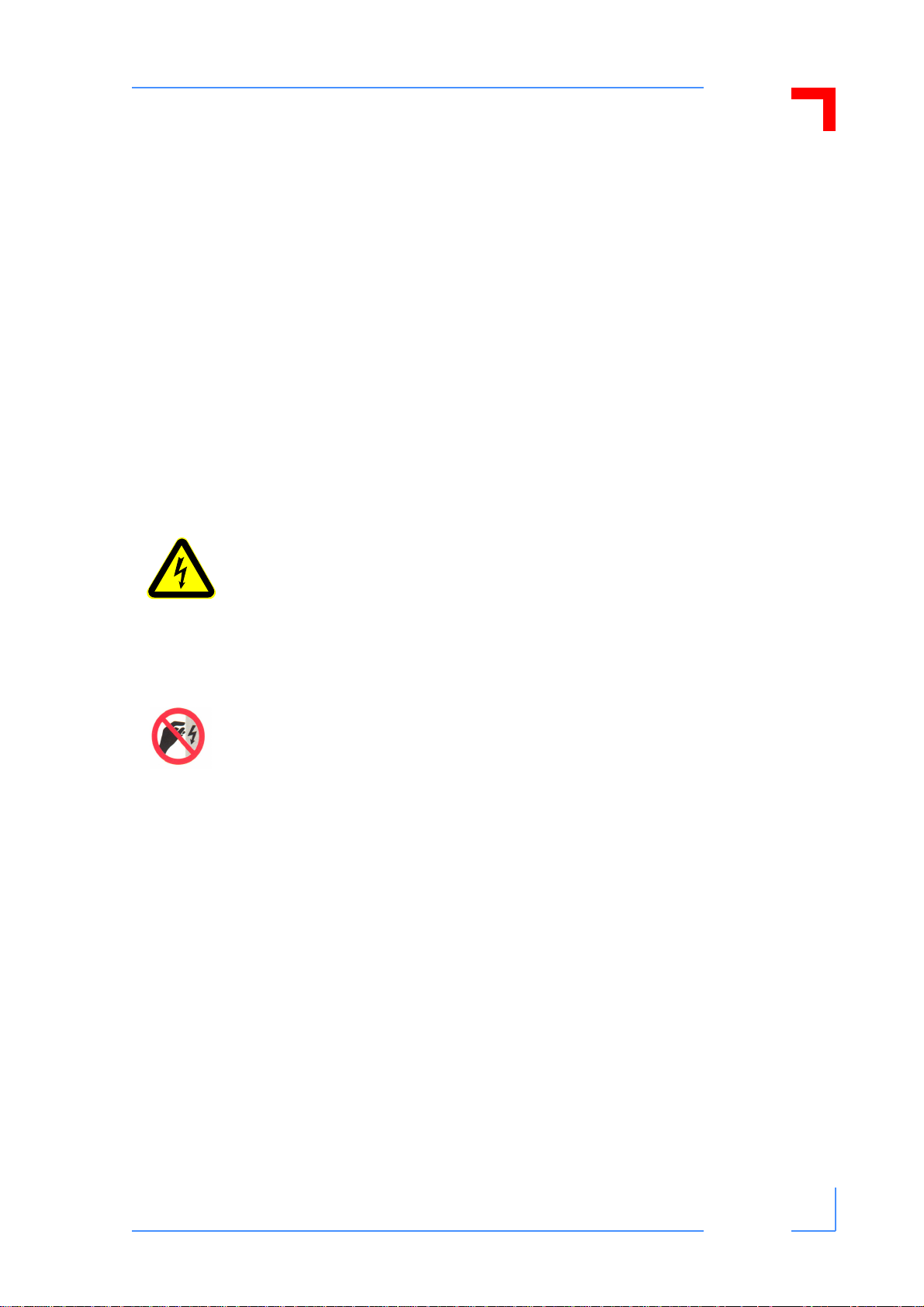
Caution, Electric Shock!
This symbol and title warn of hazards due to electrical shocks (> 60V)
when touching products or parts of them. Failure to observe the precautions indicated and/or prescribed by the law may endanger your
life/health and/or result in damage to your material.
Please refer also to the section “High Voltage Safety Instructions” on
the following page.
Warning, ESD Sensitive Device!
This symbol and title inform that electronic boards and their components are sensitive to static electricity. Therefore, care must be taken
during all handling operations and inspections of this product, in
order to ensure product integrity at all times.
Please read also the section “Special Handling and Unpacking
Instructions” on the following page.
Warning!
This symbol and title emphasize points which, if not fully understood
and taken into consideration by the reader, may endanger your health
and/or result in damage to your material.
Note...
This symbol and title emphasize aspects the reader should read
through carefully for his or her own advantage.
Page xii © 2002 PEP Modular Computers GmbH ID 24208, Rev. 01
Page 13
CP382 Preface
For Your Safety
Your new PEP product was developed and tested carefully to provide all features necessary to
ensure its compliance with electrical safety requirement s. It wa s also de signed for a long faultfree life. However, the life expectancy of your product can be drastically reduced by improper
treatment during unpacking and installation. Therefore, in the interest of your own safety and
of the correct operation of your new PEP product, you are requested to conform with the following guidelines.
High Voltage Safety Instructions
Warning!
All operations on this device must be carried out by sufficiently skilled
personnel only.
Caution, Electric Shock!
Before installing your new PEP product into a system always ensure
that your mains power is switched off. This applies also to the installation of piggybacks.
Serious electrical shock hazards can exist during all installation,
repair and maintenance operations with this product. Therefore,
always unplug the power cable and any other cables which provide
external voltages before performing work.
Special Handling and Unpacking Instructions
ESD Sensitive Device!
Electronic boards and their components are sensitive to static electricity.
Therefore, care must be taken during all handling operations and inspections
of this product, in order to ensure product integrity at all times.
Do not handle this product out of its protective enclosure while it is not used for operational
purposes unless it is otherwise protected.
Whenever possible, unpack or pack this product only at EOS/ESD safe work stations. Where
a safe work station is not guaranteed, it is important for the user to be electrically discharged
before touching the product with his/her hands or tools. This is most easily done by touching a
metal part of your system housing.
It is particularly important to observe standard anti-static precautions when changing piggybacks, ROM devices, jumper settings etc. If the product contains batteries for RTC or memory
back-up, ensure that the board is not placed on conductive surfaces, including anti-st atic plastics or sponges. They can cause short circuits and damage the batteries or con ductive circuit s
on the board.
ID 24208, Rev. 01 © 2002 PEP Modular Computers GmbH Page xiii
Page 14

Preface CP382
General Instructions on Usage
In order to maintain PEP’s product warranty, this product must not be altered or modified in an y
way . Changes or modifications to the device, which are not explicitly approved by PEP Modular
Computers and described in this manual or received from PEP Technical Suppo rt as a spe cial
handling instruction, will void your warranty.
This device should only be installed in or connected to systems that fulfill all necessary technical and specific environmental requirements. This applies also to the operational temperature
range of the specific board version, which must not be exceeded. If batteries are present their
temperature restrictions must be taken into account.
In performing all necessary installation and application operations, please follow only the instructions supplied by the present manual.
Keep all the original packaging material for future storage or warranty shipment s. If it is necessary to store or ship the board please re-pack it as nearly as possible in the manner in which it
was delivered.
Special care is necessary when handling or unp acking the product. Please, consult the special
handling and unpacking instruction on the previous page of this manual.
Page xiv © 2002 PEP Modular Computers GmbH ID 24208, Rev. 01
Page 15

CP382 Preface
Two Year Warranty
PEP Modular Computers grants the original purchaser of PEP products a TWO YEAR LIMITED
HARDWARE
granted or implied by anyone on behalf of PEP are valid unless the consumer has the express
written consent of PEP Modular Computers.
PEP Modular Computers warrants their own product s, excluding software, to be free from manufacturing and material defects for a period of 24 consecutive months from the date of purchase. This warranty is not transferable nor extendible to cover any other users or long-term
storage of the product. It does not cover products which have been modified, altered or repaired by any other party than PEP Modular Computers or their authorized agents. Furthermore, any product which has been, or is suspected of being damaged as a result of neg ligence,
improper use, incorrect handling, servicing or maintenance, or which has been damaged as a
result of excessive current/voltage or temperature, or which has had its serial number(s), any
other markings or parts thereo f altered, defaced or removed will also be excluded from this warranty.
WARRANTY as described in the fo llowing. However, no other warranties that may be
If the customer’s eligibility for warranty has not been voided, in the event of any claim, he may
return the product at the earliest possible convenience to the original place of p urchase, together with a copy of the original document of purchase, a full description of the application the
product is used on and a description of the defect. Pack the product in such a way as to ensure
safe transportation (see our safety instructions).
PEP provides for repair or replacement of any part, assembly or sub-assemb ly at their own discretion, or to refund the original cost of purchase, if appropriate. In the event of repair , refunding
or replacement of any part, the ownership of the removed or replaced parts reverts to PEP
Modular Computers, and the remaining part of the original guarantee, or any new guarantee to
cover the repaired or replaced items, will be transferred to cover the new or repaired items. Any
extensions to the original guarantee are considered gestures of goodwill, and will be defined in
the “Repair Report” issued by PEP with the repaired or replaced item.
PEP Modular Computers will not accept liability for any further claims resulting directly or indirectly from any warranty claim, other than the above specified rep air , replacement or refunding.
In particular, all claims for damage to any system or process in which the product was employed, or any loss incurred as a result of the product not functioning at any given time, are
excluded. The extent of PEP Modular Computers liability to the customer shall not exceed the
original purchase price of the item for which the claim exists.
PEP Modular Computers issues no warranty or representation, either explicit or implicit, with
respect to its products’ reliability, fitness, quality, marketability or ability to fulfil any particular
application or purpose. As a result, the products are sold “as is,” and the responsibility to ensure
their suitability for any given task remains that of the purchaser. In no event will PEP be liable
for direct, indirect or consequential damages resulting from the use of our hardware or software
products, or documentation, even if PEP were advised of the possibility of such claims prior to
the purchase of the product or during any period since the date of its purchase.
Please remember that no PEP Modular Computers employee, dealer or agent is authorized to
make any modification or addition to the above specified terms, either verbally or in any other
form, written or electronically transmitted, without the company’s consent.
ID 24208, Rev. 01 © 2002 PEP Modular Computers GmbH Page xv
Page 16

Preface CP382
This page was intentionally left blank.
Page xvi © 2002 PEP Modular Computers GmbH ID 24208, Rev. 01
Page 17

CP382 Introduction
Chapter
1
Introduction
ID 24208, Rev. 01 © 2002 PEP Modular Computers GmbH Page 1 - 1
Page 18

Introduction CP382
This page was intentionally left blank.
Page 1 - 2 © 2002 PEP Modular Computers GmbH ID 24208, Rev. 01
Page 19

CP382 Introduction
1. Introduction
1.1 Product Overview
The CP382 digital output controller has been designed to provide a large number of automatically controlled, flexible digital outputs within a ruggedised board equipped with features for
electrical protection. The flexibility is due to the fact that the 24 channels provided are organised into 3 separate clusters of 8 channels each, allowing the user to configure up to 3 different
voltages as required. Reliability is assured by features which include overtemperature thermal
shutdown, overcurrent and undervoltage protection. Use of the widely available D-sub 6 2 front
panel connector means that the board may be used in a broad range of application fields. On
the software side the board may be used with all major operating systems.
This product is part of a comprehensive concept whose goal is to provide Comp actPCI system
integrators with a complete range of I/O products which include the functions of analog input,
analog output, digital input and digital output implemented as separate integral boards. This
concept ensures the maximum degree of system design flexibility thus allowing for the ef ficient
and effective usage of available resources..
Table 1-1: CP382 Main Features
FEATURE DESCRIPTION
Channels 24 digital output channels in 3 independent groups of 8 channels
each. Each group may be set to operate at different voltages for different loads within the prescribed output voltage limits.
Protective Features The design of the board incorporates a range of protective features
including the following:
Signal Output Overcurrent Protection
Input Voltage Undervoltage Protection
Overtemperature Protection
Isolation: system side protected by optocouplers
Details of these protective features are provided in table 1-4, Digital
Output Specifications
External Interfaces 2 external interfaces, the digital output interface connector CON2 on
the front panel and a single CompactPCI connector at the rear.
The digital output interface connector supports up to 24 digital output
channels. The connector pins are subdivided into 3 clusters or groups
which are independent from each other and can operate at different
voltages to meet the requirements of different loads.
The CompactPCI connector is the standard CPCI type connector for J1
Indicators One green LED (Run) and one red LED (Fail), which are user config-
urable
Temperature Range The board is qualified to operate over a wide range of temperatures
as follows:
Operational: 0ºC to +70ºC Standard
-40ºC to +85ºC E2
Storage: -55ºC to +125ºC
ID 24208, Rev. 01 © 2002 PEP Modular Computers GmbH Page 1 - 3
Page 20

Introduction CP382
1.2 Board Overview
1.2.1 Board Introduction
The CP382 is a digital output board which provides twenty-four output channels grouped into
three clusters of eight channels each. The major components involved are the front end High
Side Driver switches (HSD = High Side Driver switch), output signal optoisolation, and the Digital Output Process and Communications (DO ProComm) controller which is realized within a
Field-Programmable Gate Array (FPGA). The DO ProComm Controller is designed for effective and efficient control of the digital output signals as well as providing interfacing with the
CPCI system controller.
Digital output requests from the System Controller are processed accordingly by the DO ProComm controller and are then routed to the HSD’s which in turn create the actual digit al output
utilizing the external supply voltage as the power source.
An external reset input is provided to simultaneously switch off all the outputs per cluster and
sets all the High Side Driver Switches to open. Each cluster has its own separate reset signal
input.
This reset can be used by the application to keep the inputs low after a fault condition.
1.2.2 Board Specific Information
Specific board components involved in the digital output process:
• One front panel connector (62-pin, female, D-sub type)
• 6 HSD switches (4 channels per switch, 2 switches per cluster)
• Optoisolation for each output channel
• One FPGA (the DO ProComm controller)
• One CompactPCI bus connector (J1, board to backplane, 132-pin, female, six row)
• One EEPROM (CapROM)
1.3 System Relevant Information
The following system relevant information is general in nature but should still be considered
when developing applications using the CP382.
Table 1-2: System Relevant Information
SUBJECT INFORMATION
System Configuration The CP382 operates with a system clock frequency of 33 MHz.
The maximum number of CP382’s which may be installed in any one system
depends on the system configuration.
Master/Slave Functionality The CP382 functions only as a slave. As such it requires a system master for
servicing.
System Controller The CP382 cannot function as a system controller.
Voltage Source The voltage source for the CP382 must conform with the specifications set
forth in this manual.
Page 1 - 4 © 2002 PEP Modular Computers GmbH ID 24208, Rev. 01
Page 21

CP382 Introduction
1.3.1 System Configuration
The external supply voltage (VCC) used as the output voltage on the CP382, must be within
the specified supply voltage range. In addition, it should be a DC supply with good ripple and
noise characteristics. Please refer to chapters 4 and 5 for further information.
1.3.2 Driver Software
The CP382 is supplied with appropriate driver software which provides software interfacing
with the system master.
1.4 Board Diagrams
The following diagrams illustrate board functionality and component layout.
1.4.1 Front Panel
Figure 1-1: CP382 Front Panel
CP 382
RUN FAIL
A green “Run” LED and a red “Fail” LED have been placed on the
front panel, to cater for the most likely use of these LED’s. However ,
they are user configurable and may be employed for user defined
purposes.
ID 24208, Rev. 01 © 2002 PEP Modular Computers GmbH Page 1 - 5
Page 22
Introduction CP382
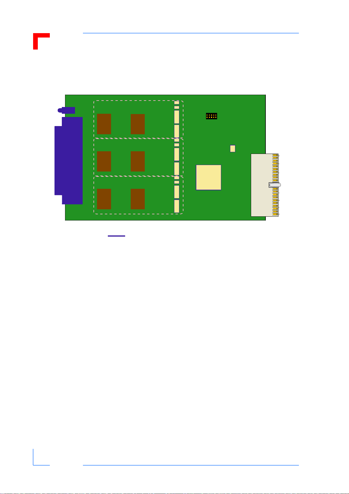
1.4.2 Board Layout
Figure 1-2: CP382 Board (Front View)
LED1
C
O
N
2
CLUSTER A
Switches
CLUSTE R B
Switches
CLUSTE R C
Switches
OPTO
OPTO
OPTO
O
P
T
O
O
P
T
O
O
P
T
O
O
P
T
O
O
P
T
O
O
P
T
O
NOTE
CON3 is a test connector for manufacturer’s use only
DO
ProComm
Controller
CON3
CapROM
25
C
O
N
1
1
Page 1 - 6 © 2002 PEP Modular Computers GmbH ID 24208, Rev. 01
Page 23
CP382 Introduction
1.5 Technical Specifications
Table 1-3: CP382 Main Specifications
GROUP/
INTERFACE
DO ProComm
Controller and
Related
Peripheral
Memory
CompactPCI
Interface
(See note at foot
of table)
Digital Output
Interface
Indicators Front Panel LED’s One green and one red LED to indicate operational status
FPGA Logic Device Provides CompactPCI interfacing and IO control logic
CapROM 4 kBit (512 byte) EEPROM
Realized on 132-pin,
female, six row connector (standard CPCI type
connector for J1)
One 62-pin, female,
three row, D-sub connector
TYPE DESCRIPTION
Bus Width: 32-bit, Bus Speed: 33 MHz
64 kB memory space, non-prefetchable
PCI Header:
Device ID: 0x5555
Vendor ID: 0x1556
Class Code: 0x110000
Subsystem Device ID: 0x00F0
Subsystem Vendor ID: 0x1518
Supports up to 24 digital output channels
General
Form Factor 3U, 4HP
Mechanical Conforms with IEEE 1101.1
System Power Con-
sumption
Temperature Range Operational: 0ºC to +70ºC Standard
Humidity 0% to 95% non-condensing
Dimensions 100 mm x 160 mm single height Eurocard
Board Weight 155 grams
+ 3.3V: maximum 860 mW (all 24 channels activated)
-40ºC to +85ºC E2
Storage: -55ºC to +125ºC
Note...
The Device ID and Vendor ID refer to the chip manufacturer. In the Class Code
value given, “11” relates to the data acquisition and signal processing controllers and “0000” relates to the DPIO modules. Subsystem Device ID and Subsystem Vendor ID are defined by PEP.
ID 24208, Rev. 01 © 2002 PEP Modular Computers GmbH Page 1 - 7
Page 24
Introduction CP382
Table 1-4: CP382 Digital Output Specifications
TYPE DESCRIPTION
Output Voltage Range Low state: =< +1.5 V
High state: > +8.0 V and < +35 V
Current per channel: max. 0.5 A
Leakage current: 20 µA
Channels 24 channels grouped into three clusters of eight channels each
Channel Connections 1 pin per channel
External Reset The output of each cluster has two means of being halted:
• externally via the EXTRESET signal
• internally on request from the application via the DO ProComm
controller
External Voltage +9.5 V to +35 V
Switch “On” Resistance R
Max Output Frequency 2.5 kHz
System Switching Delay Time T
Signal Output
Overcurrent Protection
Undervoltage Protection for
external power supply
Overtemperature If the case temperature of the High Side Driver switches exceeds 150°C the
Isolation 2 kV process to system
= 1.8 Ohm
ds,on
= 4 µs, T
d,on
For output currents of greater than 0.8 A, the output will be switched to a failure mode: square wave signal with a maximum current amplitude of 0.4A and
an on/off time (t
This type of system failure indication is made available to the DO ProComm
controller.
For the voltage source (EXTVCC) <= +8.5V, the outputs are switched off
This type of system failure indication is made available to the DO ProComm
controller.
outputs are switched off
This type of system failure indication is made available to the DO ProComm
controller.
d,off
on, toff
= 90 µs
) of 100 µs.
1.6 Software Support
The CP382 is supplied with appropriate driver software which provides software interfacing to
the system master. The CP382 supports Windows XP
Linux.
Page 1 - 8 © 2002 PEP Modular Computers GmbH ID 24208, Rev. 01
, Windows NT 4.0, VxWorks and
Page 25
CP382 Introduction
1.7 Applied Standards
The PEP Modular Computers’ CompactPCI systems comply with the requirements of the following standards:
Table 1-5: Applied Standards
TYPE STANDARD
Emission EN50081-1
CE
MECHANICAL Mechanical Dimensions IEEE 1101.1
ENVIRONMENTAL TESTS
Immunity, Industrial Environment EN50082-2
Immunity, IT Equipment EN55024
Electrical Safety EN60950
Vibration, Sinusoidal IEC68-2-6
Random Vibration, Broadband IEC68-2-64 (3U boards)
Permanent Shock IEC68-2-29
Single Shock IEC68-2-27
1.8 Related Publications
Table 1-6: Related Publications
ISSUED BY DOCUMENT
CompactPCI
Systems
CP382
PICMG CompactPCI Specification, V. 2.0, Rev. 3.0
PEP Modular Computers CompactPCI Systems Manual (ID 19953)
ST Microelectronics L6376 0.5A High-Side Driver Quad Intelligent Power
Switch
ID 24208, Rev. 01 © 2002 PEP Modular Computers GmbH Page 1 - 9
Page 26

Introduction CP382
This page was intentionally left blank.
Page 1 - 10 © 2002 PEP Modular Computers GmbH ID 24208, Rev. 01
Page 27

CP382 Functional Description
Chapter
2
Functional Description
ID 24208, Rev. 01 © 2002 PEP Modular Computers GmbH Page 2 - 1
Page 28

Functional Description CP382
This page was intentionally left blank.
Page 2 - 2 © 2002 PEP Modular Computers GmbH ID 24208, Rev. 01
Page 29

CP382 Functional Description
2. Functional Description
The following sections present more detailed, board level information about the CP382 Digital
Output controller whereby the board components and their basic functionality are discussed in
general.
2.1 General Information
The CP382 is comprised basically of the following:
• High Side Driver switches
• Optocouplers
• DO ProComm controller
• Controls digital output and provides interfacing to the CompactPCI bus
• System interfaces for:
• Front Panel
• 24 channels of digital outputs
• External supply connection for each cluster
• External hardware reset for each cluster
• One 62-pin, female, 3-pin row, D-sub connector (CON2)
• CompactPCI bus
• 132-pin, female, 6-pin row connector (CON1)
• CompactPCI specification
• On board memory: Capability EEPROM (CapROM)
• Monitor and Control
• Two operational status LED’s
• External reset
• Output failure indicators
• Software
ID 24208, Rev. 01 © 2002 PEP Modular Computers GmbH Page 2 - 3
Page 30

Functional Description CP382
2.1.1 High Side Driver Switches
The High Side Driver switches (HSD switches) are able to drive inductive, capacitive or resistive loads. Diagnostic information for the system master and extensive use of electrical protection are among their main characteristics.
The HSD switches (type L6376 manufactured by SGS THOMSON) constitute the most important part of the front end. The L6376 switch realizes a QUAD intelligent power switch which
adapts the digital output signals to the prevailing voltage and current levels and also provides
corresponding mechanisms to protect against undervoltage, overcurrent and overtemperature.
The output voltage level is adapted to the external supply volt age for high level and for low level
output voltage respectively via the integrated FET transistor output stage within the HSD
switch. The HSD switch implements a clamp diode for inductive load driving.
The voltage source for the CP382 front end is implemented using an external voltage source
(nominal +24V, also in the range +9.5V to +35V).
The input signals to the HSD switches are derived from the system side, directly from the outputs of the optocoupler devices.
2.1.2 Optoisolation
The process side is galvanically isolated from the system side. The process side of the board
is separated from the system side by a bank of optocouplers which serve to protect the system
side from any excess voltages or voltage spikes.
2.1.3 DO ProComm Controller
The DO ProComm controller is responsible for supervising and controlling the digit al data output process and maintaining communication with the CompactPCI system master . Applications
address the CP382 through its software driver interface within the system master where by the
controller accepts requests from the driver and executes them accordingly . Digit al data from the
system master is processed through the DO ProComm controller and then routed to the HSD
switches.
Page 2 - 4 © 2002 PEP Modular Computers GmbH ID 24208, Rev. 01
Page 31

CP382 Functional Description
2.1.4 System Interfaces
The CP382 provides interfacing capability for the following system elements:
• Front Panel connector
• CompactPCI bus
Digital outputs, external voltage, and external reset are routed via the CON2 connector. Interfacing to the CompactPCI bus is accomplished via the CON1 connector . Test a nd program development is supported by the CON3 connector.
External supply each Cluster:
The connection for the external supply (+24V DC [9.5V to 35V] each cluster) is realized by re-
served/ defined pins within each cluster at the front panel connector CON2.
Important...
In addition to supplying the current for the logic parts of the power switches
which are linked to the digital outputs, the exte rnal volt age su pplies also have to
supply the current for the 8 digital output loads per cluster.
External reset for each cluster:
The digital outputs will be brought to zero output level on power-up. In addition to the reset by
software, the reset-lines (one each cluster) are routed to the front panel.
2.1.5 Monitor and Control
Various monitor and control functions are available for the operation of the CP382. T wo LED’s
are available for operator interaction. There are also system failure indicators available. In addition, applications have access via the System Master driver software to board specific registers.
2.1.6 Software
Driver software is available for the System Master application software.
ID 24208, Rev. 01 © 2002 PEP Modular Computers GmbH Page 2 - 5
Page 32

Functional Description CP382
2.2 Board Level Interfacing Diagram
The following figure demonstrates the interfacing structure between the internal processing
modules of the CP382 and other major CP382 system components. Where CP382 system elements have common interfacing they are grouped into a block. Interfacing common to only
one element of a block is indicated with a direct connecting line. The interfacing lines are shown
in white where they are onboard and in black for board external interfacing.
Figure 2-1: CP382 Board Level Interfacing
CP382 Digital Output Controller
CPCI - Interface
DO ProComm Controller
CLUSTER A
HSD
Switch
Outputs
A0...A7
Opto-isolation
HSD
Switch
Outputs
B0...B7
CLUSTER CCLUSTER B
HSD
Switch
Outputs
C0...C7
Reset &
Supply Voltage
Reset &
Supply Voltage
Reset &
Supply Voltage
Digital Output
NOTE
HSD = High Side Driver switch
Page 2 - 6 © 2002 PEP Modular Computers GmbH ID 24208, Rev. 01
Page 33

CP382 Functional Description
2.3 System Interfaces
2.3.1 Digital Output Interface
The digital output interface is routed through the CON2 connector. The following figure and table indicate the pin layout and pinout of this connector.
Figure 2-2: Pin Layout of the Digital Output Interface Connector CON2
0
1
CP 382
2
5
+
+
3
4
6
7
+
+
CLUSTER A
RUN FAIL
KEY
= GND
R = Reset
NC
NC
NC
NC
NC
R
2
5
+
+
R
2
5
+
+
R
NC
NC
NC
NC
NC
NC
0
1
3
4
6
7
+
+
0
1
3
4
6
7
+
+
NC
NC
NC
NC
NC
NC
CLUSTER B
CLUSTER C
+ = VCC
Pin 43
Pin 1
Note: Each cluster has its own
external reset and external
Pin 22
supply voltage (VCC and GND).
They are not connected with each other
on the CP382.
ID 24208, Rev. 01 © 2002 PEP Modular Computers GmbH Page 2 - 7
Page 34

Functional Description CP382
Table 2-1: Pinout of the Digital Output Interface Connector CON2
CLUSTER PIN SIGNAL PIN SIGNAL PIN SIGNAL
1NC 22 NC
2NC 23 NC 43 NC
3NC 24 NC 44 NC
4NC 25 NC 45 NC
5NC 26 NC 46 NC
6NC 27 NC 47 NC
7 EXTGND_C 28 EXTGND_C 48 EXTRESET_C
8 EXTVCC_C 29 EXTVCC_C 49 EXTVCC_C
CLUSTER C
CLUSTER B
CLUSTER A
9 DOUT_C6 30 DOUT_C7 50 EXTVCC_C
10 DOUT_C3 31 DOUT_C4 51 DOUT_C5
11 DOUT_C0 32 DOUT_C1 52 DOUT_C2
12 EXTGND_B 33 EXTGND_B 53 EXTRESET_B
13 EXTVCC_B 34 EXTVCC_B 54 EXTVCC_B
14 DOUT_B6 35 DOUT_B7 55 EXTVCC_B
15 DOUT_B3 36 DOUT_B4 56 DOUT_B5
16 DOUT_B0 37 DOUT_B1 57 DOUT_B2
17 EXTGND_A 38 EXTGND_A 58 EXTRESET_A
18 EXTVCC_A 39 EXTVCC_A 59 EXTVCC_A
19 DOUT_A6 40 DOUT_A7 60 EXTVCC_A
20 DOUT_A3 41 DOUT_A4 61 DOUT_A5
21 DOUT_A0 42 DOUT_A1 62 DOUT_A2
Page 2 - 8 © 2002 PEP Modular Computers GmbH ID 24208, Rev. 01
Page 35

CP382 Functional Description
2.4 CapROM EEPROM
The CapROM is a 4 kBit (512 byte) EEPROM which provides the capability t o store board control relevant information to allow software configuration of the CP382.
2.5 Monitor and Control (M/C)
The front panel of the board is equipped with two LED’s for user defined purpose s. One green
(RUN) and one red (F AIL) have been placed on the front panel in anticipation of their most likely
use. However they are freely programmable, the indicators being selected by the system master (access to the hardware debug register (hdr)).
The system failure indicators regarding undervoltage, overcurrent and overtemperature are
made available to the DO ProComm controller . These indicators are aut omatically reset by the
HSD switches once the conditon has been corrected and the output returns to normal mode.
An input signal Halt/Reset is available to set an inactive state for each individual cluster and
also to shut down each individual cluster during operation as necessary.
ID 24208, Rev. 01 © 2002 PEP Modular Computers GmbH Page 2 - 9
Page 36

Functional Description CP382
This page was intentionally left blank.
Page 2 - 10 © 2002 PEP Modular Computers GmbH ID 24208, Rev. 01
Page 37

CP382 Installation
Chapter
3
Installation
ID 24208, Rev. 01 © 2002 PEP Modular Computers GmbH Page 3 - 1
Page 38

Installation CP382
This page was intentionally left blank.
Page 3 - 2 © 2002 PEP Modular Computers GmbH ID 24208, Rev. 01
Page 39
CP382 Installation
3. Installation
The CP382 has been designed for easy installation. However, the following standard precautions, installation procedures and general information must be observed to ensure proper installation and to preclude damage to the board or injury to personnel.
3.1 Hardware Installation
The product described in this manual can be installed in any available 3U slot of a CompactPCI
system except for the system master slot.
3.1.1 Safety Requirements
The board must be securely fastened to the chassis using the two front panel retaining screws
located at the top and bottom of the board to ensure proper grounding and to avoid loosening
caused by vibration or shock.
In addition the following electrical hazard precautions must be observed.
Caution, Electric Shock Hazard!
Ensure that the system main power is removed prior to installing or removing
this board. Ensure that there are no other external voltages or signals being
applied to this board or other boards within the system. Failure to comply with
the above could endanger your life or health and may cause damage to this
board or other system components.
ESD Equipment!
This PEP board contains electrostatically sensitive devices. Please observe
the following precautions to avoid damage to your board:
Discharge your clothing before touching the assembly. Tools must be
discharged before use.
Do not touch any on board components, connector pins, or board conductive
circuits.
If working at an anti-static workbench with professional discharging
equipment, ensure compliance with its usage when handling this product.
ID 24208, Rev. 01 © 2002 PEP Modular Computers GmbH Page 3 - 3
Page 40

Installation CP382
3.1.2 Installation Procedures
To install the board proceed as follows:
1. Ensure that the safety requirements indicated above are observed.
Warning!
Failure to comply with the instruction below may cause damage to the board or
result in improper system operation. Please refer to chapters 4 and 5 for configuration information.
2. Ensure that the board is properly configured for operation before installing.
Note...
Care must be taken when applying the procedures below to ensure that when
the board is inserted it is not damaged through contact with other boards in the
system.
3. To install the board perform the following:
1. Prior to installation of the board disengage the insertion/extraction handle by first unlocking the handle and pressing it down.
2. Insert the board into an appropria te slot, and, using the insertion/extraction handle, ensure that it is properly seated in the backplane. (Front panel is flush with the rack front;
the insertion/extraction handle is locked.)
4. Fasten the front panel retaining screws.
5. Connect external interfacing cables to the board as required.
6. Ensure that the interfacing cables are properly secured.
Warning!
Proper and safe operation of the CP382 Digital Output Controller depends on
the correct configuration of the external voltage and loads. System integrators
must ensure that all voltages presented to the CP382 comply with the
specifications set forth in this manual.
Failure to comply with the above may cause damage to the board or result in
improper system operation. Please refer to chapters 4 and 5 for configuration
information.
Page 3 - 4 © 2002 PEP Modular Computers GmbH ID 24208, Rev. 01
Page 41

CP382 Installation
3.1.3 Removal Procedures
To remove the board proceed as follows:
1. Ensure that the safety requirements indicated above are observed.
Warning!
Care must be taken when applying the procedures below to ensure that when
the board is removed it is not damaged through contact wit h othe r board s in the
system.
2. Disconnect any interfacing cables that may be connected to the board.
3. Loosen both of the front panel retaining screws.
4. To remove the board from the backplane perform the following:
1. Unlock the insertion/extraction handle by pressing down on the grey locking mechanism in the middle of the handle. (This should be achievable with a minimum of f orce.
If necessary lift the handle up slightly while pressing down on the grey locking mechanism.)
2. Disengage the bo ard from the backplane by pressing down on the insertion/extraction
handle and pull the board out of the slot ensuring that the board does not make cont act
with adjacent boards. (If the handle does not move, it is not unlocked. Repeat the unlocking procedure above and try again. Do not use force!)
3.2 Software Installation
Installation of the CP382 driver software is a function of the application operating system. For
further information refer to the appropriate software documentation.
ID 24208, Rev. 01 © 2002 PEP Modular Computers GmbH Page 3 - 5
Page 42

Installation CP382
This page was intentionally left blank.
Page 3 - 6 © 2002 PEP Modular Computers GmbH ID 24208, Rev. 01
Page 43

CP382 Configuration
Chapter
4
Configuration
ID 24208, Rev. 01 © 2002 PEP Modular Computers GmbH Page 4 - 1
Page 44

Configuration CP382
This page was intentionally left blank.
Page 4 - 2 © 2002 PEP Modular Computers GmbH ID 24208, Rev. 01
Page 45

CP382 Configuration
4. Configuration
This chapter provides information for configuring the CP382 board for operation.
4.1 Jumper Settings
The CP382 does not have any jumpers which require configuring.
4.2 Digital Output Signal Properties
In addition to the output signal type and its range, which have been specified in chapter 1, p aragraph 1.3.1, system integrators must be aware of certain output configuration requirements for
the CP382. The following paragraphs provide some information regarding individual connection configuration requirements.
4.2.1 Channels
The CON2 connector of the CP382 is designed so that there is one output pin per channel.
This is illustrated in Figure 2-2, which shows the front panel connector pinout, with the 24 channels shown starting at the top of the connector with channel 0 (cluster A).
The following sections address the basic requirements.
4.2.2 Connection of External Supply
The CP382 requires an external voltage for operation.
The input connection for this voltage is realized via the 62-pin front panel connector CON2. The
pinout of this connector is provided in table 2-1.
The three clusters have split supply planes, so that it is possible to provide each cluster (clus-
ters A, B and C) with a separate volt age, with different voltage values within the defined range
(see also table 1-1).
Note...
Each channel has a maximum current of 0.5 A. In situations where many channels are carrying a high current, separate, larger gauge cables for the external
power supply should be used.
ID 24208, Rev. 01 © 2002 PEP Modular Computers GmbH Page 4 - 3
Page 46
Configuration CP382
4.2.3 Channel Connection
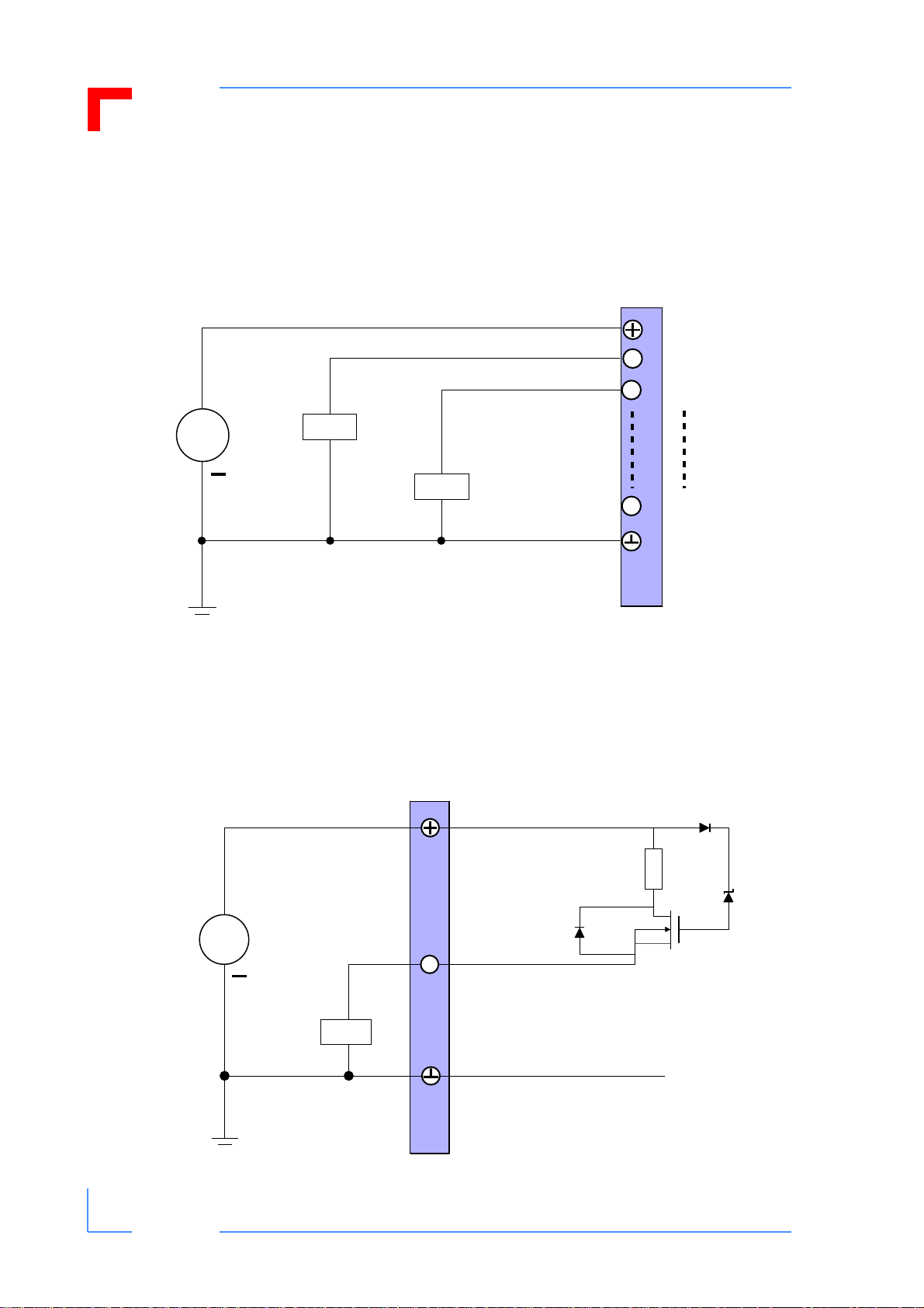
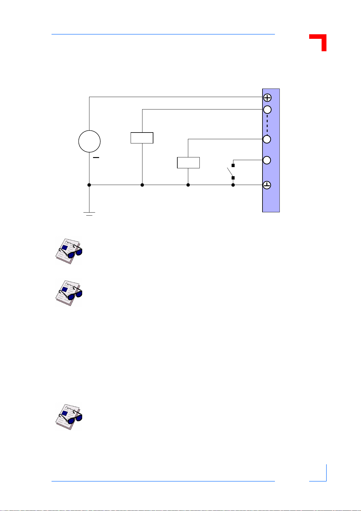
The following diagrams illustrate the external connection of the CP382 to the application.
Figure 4-1: Digital Output Connection for One Cluster
CON2
Supply Voltage
External VCC
Ch 0
0
1
Ch 1
Ch 7
7
External
VCC
+
V
LOAD
LOAD
Figure 4-2: Digital Output Circuit for One Channel
CON2
External VCC
Ch 0
0
External
VCC
Supply Voltage
+
V
EXTGND
CP382
Rds, on
LOAD
EXTGND
CP382
External GND
Page 4 - 4 © 2002 PEP Modular Computers GmbH ID 24208, Rev. 01
Page 47
CP382 Configuration
Figure 4-3: External Reset Connection for One Cluster
CON2
Supply Voltage
Ch 0
0
External
VCC
External GND
+
V
LOAD
LOAD
R
7
Ch 7
Reset
EXTGND
CP382
Note...
The voltage source for each cluster is an external supply (in the range +9.5V to
+35V DC). Therefore the GND reference for the digital output is the ground
potential of this external voltage supply.
Important...
Individual outputs should not be cascaded as it cannot be guaranteed that
power sharing will be proportional, due to the transistor characteristics of each
HSD (HighSide Driver switch).
4.2.4 Connection of Inductive Loads
The outputs have internal clamping diodes for each channel, which are able to demagnetize
inductive loads.
The limitation is the peak power dissipation of the digital outputs at the front end. Where there
are large loads or if there is the possibility that additional loads require demagnetization simultaneously, external demagnetization circuits are required.
There are two possible topologies for the demagnetization versus ground or versus supply voltage.
Note...
For more detailed information about the external demagnetization circuits,
please refer to the L6376 datasheet referenced under chapter 1.8 Related Publications.
ID 24208, Rev. 01 © 2002 PEP Modular Computers GmbH Page 4 - 5
Page 48

Configuration CP382
4.3 Programming Interface
4.3.1 Access Control Logic (Address Decoder)
All the resources of the CP382 are mapped within the 64 kB PCI memory address space which
itself is set in the PCI configuration register BAR0. The port size of all local or backend registers
is 32-bit by default. The address map of the registers is as follows.
Table 4-1: Backend Register Address Map
Base Address Size Function
bar0 + 0x0000 4 K Common Board Registers
0x0400 32 bit g_irq General Interrupt Enable Register
0x0800 32 bit hsr Hardware Status Register
0x0804 32 bit i_pen General Interrupt Pending Register
0x0c00 32 bit hdr Hardware Debug Register
bar0 + 0x1000 4 K Capability ROM, serial EEPROM
0x1000 32 bit r_cmd Command Register
0x1400 32 bit r_ctl Control Register
0x1800 32 bit r_sta Status Register
0x1c00 32 bit r_dat Data Register
bar0 + 0x2000 4 K DigOUT Cluster A
0x2400 32 bit o_ctl_a Output Control Register
0x2800 32 bit o_sta_a Output Status Register
0x2c00 32 bit o_dat_a Output Data Register
bar0 + 0x3000 4 K DigOUT Cluster B
0x3400 32 bit o_ctl_b Output Control Register
0x3800 32 bit o_sta_b Output Status Register
0x3c00 32 bit o_dat_b Output Data Register
bar0 + 0x4000 4 K DigOUT Cluster C
0x4400 32 bit o_ctl_c Output Control Register
0x4800 32 bit o_sta_c Output Status Register
0x4c00 32 bit o_dat_c Output Data Register
bar0 + 0x5000 - 0xffff 44 K Reserved
Page 4 - 6 © 2002 PEP Modular Computers GmbH ID 24208, Rev. 01
Page 49

CP382 Configuration
4.3.2 Writing Output Data
Table 4-2: Output Data Register Bit Map
Bits Type Defa ult Function
31-8 r/w 0 Reserved
7-0 r/w 0 Data, 8 bit digit
Note...
Output data is 8 bit (each cluster); this register is read/write enable.
Table 4-3: Output Control Register
Bits Type Defa ult Function
31-2 r/w 0 Reserved
1r/w0irqen
0r/w1Reset
Note...
irqen is for diagnostic issuing an interrupt.
The reset bit should be set to 0 to activate a cluster.
Table 4-4: Output Status Register, Bit Map
Bits Type Defa ult Function
31 r 0 Fail
30 r 0 Diag
29-0 r 0 Reserved
Note...
The Diag status flag is the diagnostic bit from the HSD switch; Fail is the latched
diag status flag.
ID 24208, Rev. 01 © 2002 PEP Modular Computers GmbH Page 4 - 7
Page 50

Configuration CP382
4.3.3 Hardware Debug/Test Registers
These registers are for internal test and debug only. The Common Status Register contains
Logic-V ersion and PCB -V ersion. The Common Debug Register is a read/write register without
any further functionality besides the front panel monitor and control LED’s.
Table 4-5: Hardware Debug Register Bit Map
Bits Type Default Function
31-2 r/w 0 Reserved
1r/w0FAIL
0r/w0RUN
Table 4-6: Hardware Status Register Bit Map
Bits Type Default* Function
31-16 r 0 Reserved
15-8 r 00 HW Version (PCB Index)
7-0 r 01 Logic Version
Note...
The HW version starts with 0, the Logic version starts with 1. At each further
release it will be incremented by 1.
Page 4 - 8 © 2002 PEP Modular Computers GmbH ID 24208, Rev. 01
Page 51

CP382 Configuration
4.3.4 Generating Interrupts
A detected fail flag set in the register can trigger an interrupt.
1. Check if the board is the cause of the interrupt (General Interrupt Pending is set)
2. If yes, check the reason for the interrupt by reading the fail flag in the output status register
3. Reset the corresponding Flag by writing a 1 to a set status bit (fail).
4. Reset the boards’ IRQ by resetting the General Interrupt Pending Bit by writing a 1 to that
status bit
5. Return from Interrupt
Table 4-7: General Interrupt Enable Register, Bit Map
Bits Type Defa ult Function
31 r/w 0 Board Interrupt Enable
29 - 0 r/w 0 Reserved
Note...
The board will continue issuing an interrupt until all interrupt sources are completely dealt with and no interrupt condition remains.
A set bit means that the boards’ interrupt is enabled.
Table 4-8: General Interrupt Pending Register, Bit Map
Bits Type Defa ult Function
31 r/w 0 Board Interrupt Pending
29 - 0 r/w 0 Reserved
Note...
A set bit means that the boards’ interrupt is pending. A board interrupt must be
cleared by writing a "1" to the corresponding output irqen event flag.
Table 4-9: Output Status Register, Bit Map
Bits Type Defa ult Function
31 r 0 Fail
30 r 0 Diag
29 - 0 r 0 Reserved
ID 24208, Rev. 01 © 2002 PEP Modular Computers GmbH Page 4 - 9
Page 52

Configuration CP382
4.3.5 Programming the Board Capabili ty ROM
The Board Capability ROM contains all the board data necessary to identify board, version, optional features, etc., and to setup the basic software. The BCR is implemented using a 4 KBit
serial EEPROM of the type Microchip 93LC66.
(The contents list of the BCR is not described here.)
The serial interface of the device has been realized in hardware resulting in a very simple register based programming interface with command, control, st atus and dat a registe rs. All protocol and serial timing specifications are resolved by hardware.
Programming of the BCR is undertaken as follows: The control word is written into the ROM
Control Register including command opcode and internal address. Then optional data (in case
of Write action) is written into the ROM Data Register. Command execution is started by setting
the St artbit in the ROM Command Register. Then Ready/Busy must be polled in the ROM Status Register. After reaching Ready status, the next command can be set up and data (in case
of Read action) can be fetched from the ROM Data Register.
Table 4-10: ROM Command Register Bit Map
Bits Type Default Function
31 r/w 0 Startbit
30-0 r/w 00 Reserved
Note...
The Startbit will be automatically reset as soon as an action is completed.
Table 4-11: ROM Control Register Bit Map
Bits Type Default Function
31-19 r/w 0 Reserved
17-16 r/w 00 Opcode
15-8 r/w 00 Reserved
8-0 r/w 00 Internal address (A8..A0)
Note...
The commands READ, EWEN (Write Enable) and WRITE are sufficient for all
purposes.
Page 4 - 10 © 2002 PEP Modular Computers GmbH ID 24208, Rev. 01
Page 53

CP382 Configuration
Table 4-12: Opcodes and Commands
Opcode A8..A0 Command
00 11xxxxxxx EWEN
10 xxxxxxxxx READ
01 xxxxxxxxx WRITE
Note...
The EWEN (Erase and Write Enable) command must be executed once before
the first write.
Table 4-13: ROM Status Register Bit Map
Bits Type Defa ult Function
31 r/w 0 Busy/Ready
30-0 r/w 00 Reserved
Note...
As soon as the Startbit is set the Busy/Ready bit becomes active (Busy=1). It
remains set as long as the command is executed and is reset when command
execution is complete.
Table 4-14: ROM Data Register Bit Map
Bits Type Defa ult Function
31-8 r/w 0 Reserved
7-0 r/w 0 Data (for data read and write commands)
ID 24208, Rev. 01 © 2002 PEP Modular Computers GmbH Page 4 - 11
Page 54

Configuration CP382
This page was intentionally left blank.
Page 4 - 12 © 2002 PEP Modular Computers GmbH ID 24208, Rev. 01
Page 55

CP382 System Considerations
Chapter
5
System Considerations
ID 24208, Rev. 01 © 2002 PEP Modular Computers GmbH Page 5 - 1
Page 56

System Considerations CP382
This page was intentionally left blank.
Page 5 - 2 © 2002 PEP Modular Computers GmbH ID 24208, Rev. 01
Page 57

CP382 System Considerations
5. System Considerations
5.1 Introduction
In addition to the basic specification requirements for the CP382 which have been addressed
in chapter 4, system integrators need to be aware of the overall system environment and the
application needs when designing the interfacing to the CP382. The following chapters addre ss
a number of more apparent considerations which should be addressed but certainly not all of
the possible situations which may be encountered. Many of the considerations presented here
are recommendations, but some are definite requirements if the CP382 is to successfully
achieve its purpose.
5.2 General
Considerations:
1. Care must be t aken to ensure that proper grounding concept s are followed , and that the
integrity of the grounding system within the application be maintained.
2. Where possible input wiring length should be kept as short as possible.
5.3 Shielding
Considerations:
1. Input cable shielding in general is recommended.
2. The requirement s for shielding can be seen primarily as a function of the system design
and environment, but empirical results must also be considered.
3. The CON2 connector has a metal housing which is connected to the CP382 shield and
is isolated from the system ground.
4. Ensure that if shielding is used that it is not in anyway connected to the system ground.
5.4 External Power Supply
Considerations:
1. Voltage sources presented to the CP382 must be within the ranges spe cified in ch apter
1.3.1 or erroneous results will occur as well as possible damage to the CP382.
2. In addition to supplying the current for the logic parts of the power switches which are
linked to the digital outputs, the external voltage supplies also have to supply the current
for the 8 digital output loads per cluster.
5.5 Cable Interfacing
If necessary , cabling to the CP382 CON2 connector should be physically fixed to prevent strain
on the CON2 connector.
Warning!
Each channel has a maximum current of 0.5 A. In situations where many channels are carrying a high current, separate, larger gauge cables for the external
power supply should be used.
ID 24208, Rev. 01 © 2002 PEP Modular Computers GmbH Page 5 - 3
Page 58

System Considerations CP382
This page was intentionally left blank.
Page 5 - 4 © 2002 PEP Modular Computers GmbH ID 24208, Rev. 01
 Loading...