

Konka Group L32K6RW, L37K6RW, L42K6RW, MST6E16 Service Manual
SERVICE MENUAL
MODEL: L32K6RW MST6E16
L37K6RW MST6E16
L42K6RW MST6E16
▂▂▂▂▂▂▂▂▂▂▂▂▂▂▂▂▂▂▂▂▂▂▂▂▂▂▂▂▂▂▂▂▂▂
This manual is the latest at the time of printing, and does not include the
modification which may be made after the printing, by the constant
improvement of product.
CONTENTS
Number Item Pages
1 Safety Precaution.. 3-5
2 Production Instruction Book. 6-18
3 Block Diagram 19-19
4 Circuit Diagram 20-25
5 PCB layer and Component Position. 26-27
6 Explosive View 28-32
7 Basic Operations & Circuit Description 33-36
8 Simple Trouble Shoot 37-37
9 Factory Mode Setting 38-39
10 Main IC Information 40-101
11 Panel Information 102-137
12 Software Upgrade 137-140
Safety Precaution
PRECAUTIONS DURING
SERVICING
1. In addition to safety, other parts and
assemblies are specified for conformance with
such regulations as those applying to spurious
radiation. These must also be replaced only
with specified replacements.
Examples: RF converters, tuner units, antenna
selection switches, RF cables, noise-blocking
capacitors, noise-blocking filters, etc.
2. Use specified internal Wiring. Note especially:
1) Wires covered with PVC tubing
2) Double insulated wires
3) High voltage leads
3. Use specified insulating materials for hazardous
live parts. Note especially:
1) Insulating Tape
2) PVC tubing
3) Spacers (insulating barriers)
4) Insulating sheets for transistors
5) Plastic screws for fixing micro switches
4. When replacing AC primary side components
(transformers, power cords, noise blocking
capacitors, etc.), wrap ends of wires securely
about the terminals before soldering.
5. Make sure that wires do not contact heat
generating parts (heat sinks, oxide metal film
resistors, fusible resistors, etc.)
6. Check if replaced wires do not contact sharply
edged or pointed parts.
7. Make sure that foreign objects (screws, solder
droplets, etc.) do not remain inside the set.
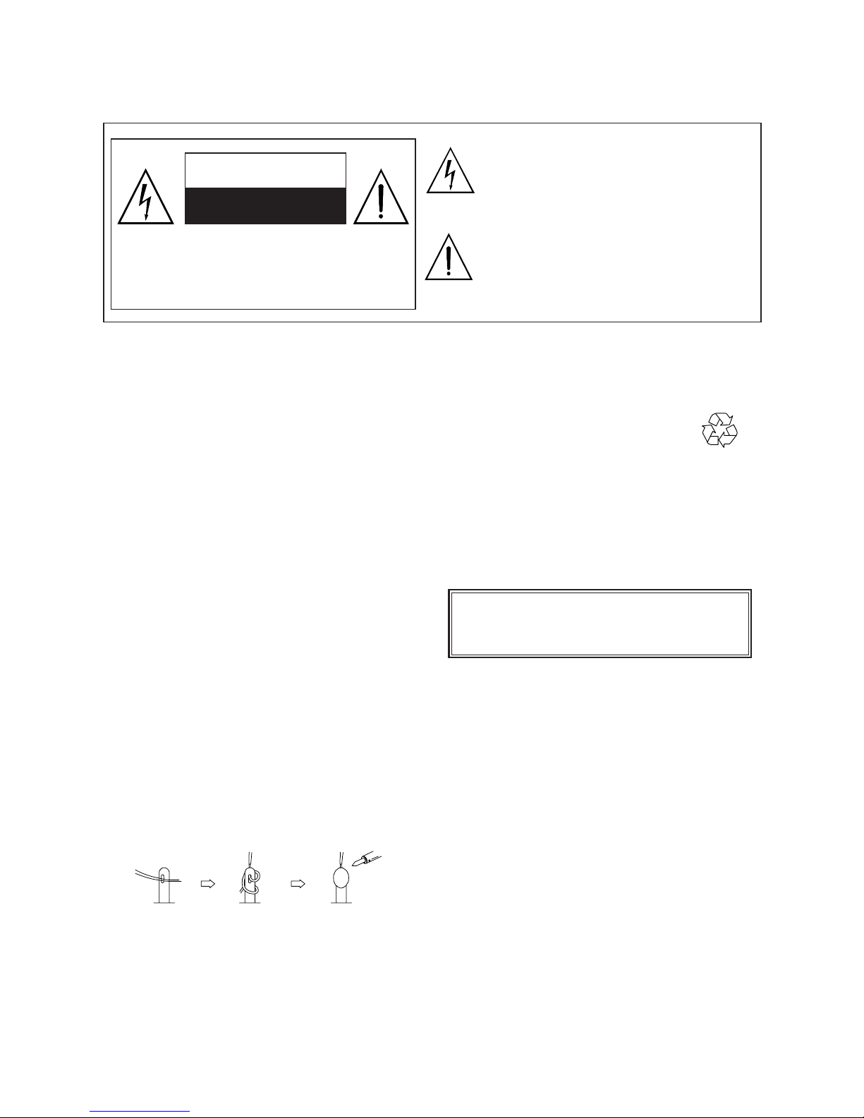
The lightning flash with arrowhead symbol,
within an equilateral triangle, is intended to
alert the user to the presence of uninsulated
“dangerous voltage” within the product’s enclo
sure that may be of sufficient magnitude to
constitute a risk of electric shock to persons.
The exclamation point within an equilateral
triangle is intended to alert the user to the
presence of important operating and
maintenance (servicing) instructions in the
literature accompanying the appliance.
CAUTION: TO REDUCE THE RISK OF
ELECTRIC SHOCK, DO NOT REMOVE COVER
(OR BACK). NO USER-SERVICEABLE PARTS
INSIDE. REFER SERVICING TO QUALIFIED
SERVICE PERSONNEL ONLY.
CAUTION
RISK OF ELECTRIC SHOCK
DO NOT OPEN
MAKE YOUR CONTRIBUTION
TO PROTECT THE
ENVIRONMENT
Used batteries with the ISO symbol
for recycling as well as small accumulators
(rechargeable batteries), mini-batteries (cells) and
starter batteries should not be thrown into the
garbage can.
Please leave them at an appropriate depot.
WARNING:
Before servicing this TV receiver, read the
SAFETY INSTRUCTION and PRODUCT
SAFETY NOTICE.
SAFETY INSTRUCTION
The service should not be attempted by anyone
unfamiliar with the necessary instructions on this
apparatus. The following are the necessary
instructions to be observed before servicing.
1. An isolation transformer should be connected in
the power line between the receiver and the
AC line when a service is performed on the
primary of the converter transformer of the set.
2. Comply with all caution and safety related
provided on the back of the cabinet, inside the
cabinet, on the chassis or picture tube.
3. To avoid a shock hazard, always discharge the
picture tube's anode to the chassis ground
before removing the anode cap.
4. Completely discharge the high potential voltage
of the picture tube before handling. The picture
tube is a vacuum and if broken, the glass will
explode.
3
PRODUCT SAFETY NOTICE
Many electrical and mechanical parts in this
apparatus have special safety-related
characteristics.
These characteristics are offer passed
unnoticed by visual spection and the protection
afforded by them cannot necessarily be obtained
by using replacement components rates for a
higher voltage, wattage, etc.
The replacement parts which have these
special safety characteristics are identified by
marks on the schematic diagram and on the parts
list.
Before replacing any of these components,
read the parts list in this manual carefully. The
use of substitute replacement parts which do not
have the same safety characteristics as specified
in the parts list may create shock, fire, or other
hazards.
9. Must be sure that the ground wire of the AC
inlet is connected with the ground of the
apparatus properly.
5. When replacing a MAIN PCB in the cabinet,
always be certain that all protective are
installed properly such as control knobs,
adjustment covers or shields, barriers, isolation
resistor networks etc.
6. When servicing is required, observe the original
lead dressing. Extra precaution should be given
to assure correct lead dressing in the high
voltage area.
7. Keep wires away from high voltage or high
tempera ture components.
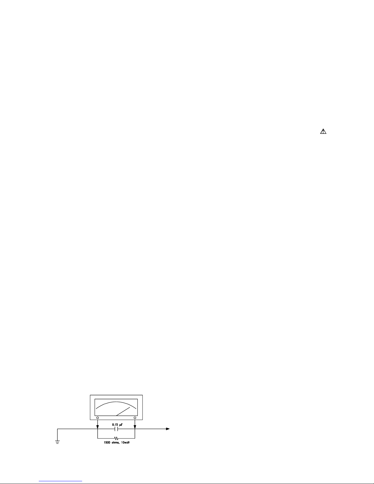
8. Before returning the set to the customer,
always perform an AC leakage current check
on the exposed metallic parts of the cabinet,
such as antennas, terminals, screwheads,metal
overlay, control shafts, etc., to be sure the set
is safe to operate without danger of electrical
shock. Plug the AC line cord directly to the
AC outlet (do not use a line isolation
transformer during this check). Use an AC
voltmeter having 5K ohms volt sensitivity or
more in the following manner.
Connect a 1.5K ohm 10 watt resistor paralleled
by a 0.15μF AC type capacitor, between a
good earth ground (water pipe, conductor etc.,)
and the exposed metallic parts, one at a time.
Measure the AC voltage across the combination
of the 1.5K ohm resistor and 0.15 uF
capacitor. Reverse the AC plug at the AC
outlet and repeat the AC voltage measurements
for each exposed metallic part.
The measured voltage must not exceed 0.3V
RMS.
This corresponds to 0.5mA AC. Any value
exceeding this limit constitutes a potential
shock hazard and must be corrected
immediately.
The resistance measurement should be done
between accessible exposed metal parts and
power cord plug prongs with the power switch
"ON". The resistance should be more than
6M ohms.
Good earth ground
such as the water
pipe, conductor,
etc.
Place this probe
on each exposed
metallic part
AC VOLTMETER
AC Leakage Current Check
4
Attention:
Motionless picture might cause permanent destruction to the display.
Be sure not to display motionless picture on the LCD TV for more than
2 hours, because it would cause picture remnants to appear, which is
called "screen burns". To avoid such picture remnants, please decrease
the "contrast" and "brightness" of the display when displaying motionless
picture.
While watching TV program in 4:3 size mode for a long time, there would
be traces on the edge of the screen's left, right and center parts because
of different transmition of the light on the screen.Similar impact on the
screen will occur when playing DVD or connecting games control. Products
destroyed by these reasons can't be guaranteed for maintenance.
It might cause picture remnants to display electronic games and motionless
picture of PC more than a period of time.To avoid such effect, please
decrease the "contrast" and "brightness" when displaying motionless
picture.
•
•
•
CAUTION
Where the MAINS plug or an appliance coupler is used as the disconnect device,
the disconnect device shall remain readily operable.
CAUTION
7KHVHVHUYLFLQJLQVWUXFWLRQVDUHIRUXVHE\TXDOL¿HGVHUYLFHSHUVRQQHORQO\7R
reduce the risk of electric shock, do not perform any servicing other than that
FRQWDLQHGLQWKHRSHUDWLQJLQVWUXFWLRQVXQOHVV\RXDUHTXDOL¿HGWRGRVR
CAUTION
Danger of explosion if battery is incorrectly replaced.
Replace only with the same or equivalent type.
%DWWHULHVVKDOOQRWEHH[SRVHGWRH[FHVVLYHKHDWVXFKDVVXQVKLQH¿UHRUWKH
like.
Used batteries should not be thrown into the garbage can, please leave them
at an appropriate depot.
5
LCD COLOR TV
1. Connection and Preparation of TV
1.1 Accessories
User Manual x 1
Power Cord x 1
Remote Control x 1
%DWWHU\8053$$$[
6WDQG[3UHDVVHPEOHG2SWLRQDO
:DOO0RXQW.LW[3UHDVVHPEOHG2SWLRQDO
1.3 Installation of Wall Mount Kit(Optional)
The Wall Mount Kit can help install the TV on the wall.
For more information about wall mounting, please refer to the instructions
provided along with the wall mount kit.
:KHQZDOOPRXQWLQJWKHSURGXFWSOHDVHFRQWDFWTXDOL¿HGSHUVRQQHO
If users choose to install the TV by themselves, the producer is irresponsible
for any possible damages caused either to the product or to persons .
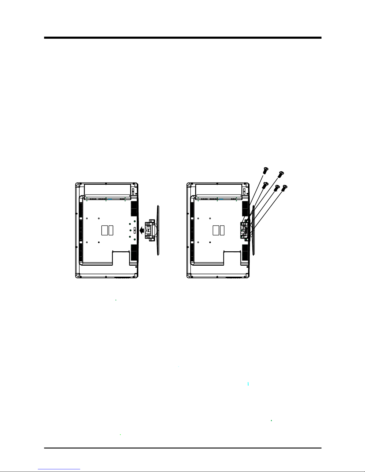
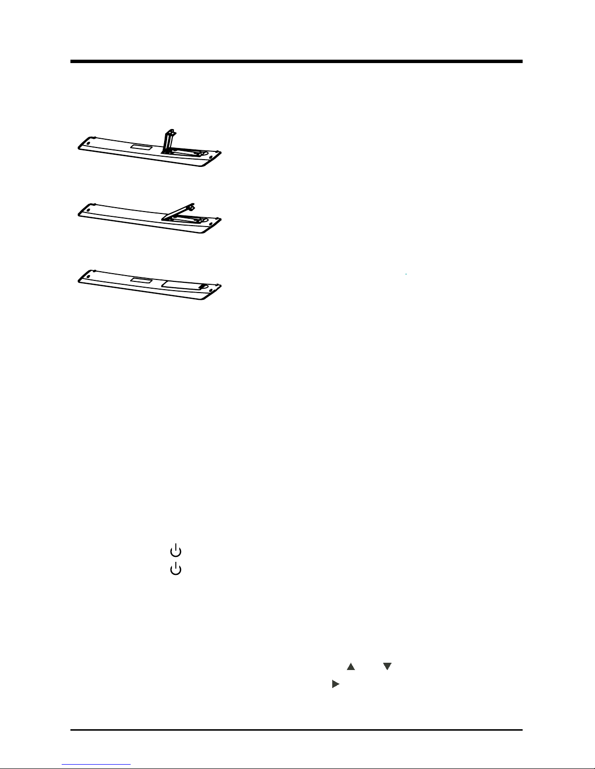
1.2 Installation of Stand
1. Place the TV with the front panel facing downwards on the soft cloth or soft
pads on a desk.
2. Insert the stand into the bottom socket of the TV.
3. Insert the screws into the sockets and tighten them.
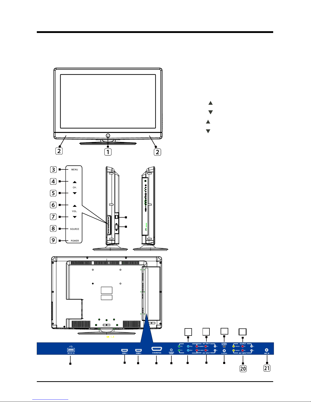
1.4 Keys and Interfaces
L32K6/L37K6/L42K6•
22
23
1. Remote sensor window&
Power indicator
2. Speaker
3. Menu key
4. Channel “
” key
5. Channel “
” key
6. Volume “
” key
7. Volume “ ” key
8. Source key
3RZHU6WDQGE\NH\
10. Power switch
11. AC input
0(',$
13. HDMI 1 input
14. HDMI 2 input
'68%9*$LQSXW
16. VGA/DVI audio input
17. YPbPr 1 and audio input
$9YLGHRDQGDXGLRLQSXW
19. S-Video input
$9YLGHRDQGDXGLRLQSXW
21. Antenna input
22. YPbPr 2 and audio input
$9YLGHRDQGDXGLRLQSXW
24.Coaxial output
$99LGHRDQGDXGLRRXWSXW
24
25
YPbPr 1
YPbPr 2
LCD COLOR TV
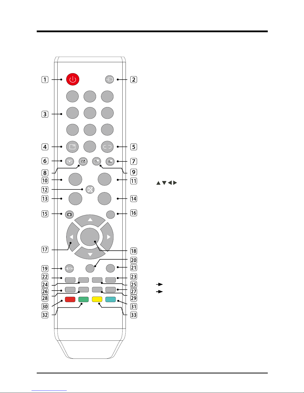
1.5 Remote Control
3
6
9
0
CH
^
P. 6,=(
>
PA*( HOLD
LIST
POS
PIP
^
1
2
4
5
7
8
0(18
ENTER
602'( 7(;7
,1'(;
5(9($/
6,=(
MI;
)5((=(
SWAP
POW(5 SOURC(
DISPLAY R(&ALL
VOL
+
_
MU7(
<(//2W
B
L
U
(
5(D
*5((1
V-CH IP
&(
CCD
P. 02'(
32:(56WDQGE\WXUQRQDQGRII
6285&(6HOHFWWKHVLJQDOVRXUFH
3. 0~9: Continue to press the keys to select
a channel.
4. DISPLAY: Display the information of
current video and audio.
5(&$//5HWXUQWRSUHYLRXVFKDQQHO
)5((=()UHH]HWKHSLFWXUH
7. PIP: Open or close PIP.
8. SWAP: Swap the position of the main
picture and sub picture.
9. POS: Change the PIP position.
10.
VOL+: Increase the volume.
11. CH∧
: Select the channel forward.
087(0XWHVRXQG
13.
VOL-: Decrease the volume.
14. CH∨
: Select the channel backward.
0(18(QWHURUH[LWPHQX
36,=(&KDQJHWKHSLFWXUHVL]H
17.
, ,
,
key: The menu item selection.
18.
(17(5&RQ¿UPRUHQWHU
602'(6HOHFWWKHVRXQGPRGH
7(;7RSWLRDO(QWHURUH[LWWHOHWH[W
&(+LGHWHOHWH[WFRQWHQWVSUHVVDJDLQWR
reappear.
302'(6HOHFWWKHSLFWXUHPRGH
23. HOLD: Hold the current page.
,1'(;'LVSOD\WKHLQGH[SDJH
3$*((QWHUWKHVXESDJHPRGH
5(9($/5HYHDOWKHKLGGHQLQIRUPDWLRQ
/,67(QWHUWKHWHOHWH[WOLVWPRGH
6,=(&KDQJHWKHWHOHWH[WVL]H
0,;3UHVVUHSHDWHGO\WRWXUQRQ7HOHWH[W
Teletext blending with TV program
Teletext mode.
5('$FFHVVWKHUHGLWHPRUSDJH
%/8($FFHVVWKHEOXHLWHPRUSDJH
*5((1$FFHVVWKHJUHHQLWHPRUSDJH
<(//2:$FFHVVWKH\HOORZLWHPRU
page.
Note: The INDEX, CE, PAGE, HOLD,
REVEAL, SIZE, MIX, LIST, RED,
GREEN, YELLOW, BLUE keys related
to teletext are optional.
2.3 Selection of Input Mode
- Press the Source button, and then press or to select the signal
source you desire, then press Enter or
EXWWRQWRFRQ¿UP
7KHVLJQDOVRXUFHVDUHGLVSOD\HGLQWKHIROORZLQJVHTXHQFH
2. Basic Operation
2.1 Power ON/OFF
- Connect the power cord to the AC Input. Insert the power cord into the
appropriate socket.
- Press the Power switch to switch on the TV, then press Power button to
turn on the unit.
- Press the Power switch again to switch off the TV.
Note: After switch off the TV, please don’t immediately re-open the power
switch ,should be delayed one minute more to re-open the power
switch.
2.2 Setting of Standby Mode
- Press Power ( EXWWRQWRWXUQRQWKHXQLW
- Press Power ( EXWWRQDJDLQWRUHWXUQWKHGLVSOD\WRVWDQGE\PRGH7KH
power indicator turns red.
- Be sure not to set your TV in standby mode for a long period of time.
1.6 Installation of Batteries
1. Open the back lid of the remote control.
,QVWDOOWZR$$$9EDWWHULHV
(QVXUHWKHFRUUHFWSRODULW\RIWKHEDWWHULHV
3. Cover the back lid.
Please take out of the batteries from the remote
control for long time of no use.
If the remote control doesn't work properly,
please carry out the following checks.
- Check the TV is turned on.
- Check the polarity of the batteries are correct.
- Check the batteries are not drained.
- Check the power supply is normal or the power cord
is correctly connected.
&KHFNWKHUHDUHQRVSHFLDOÀXRUHVFHQWOLJKWRUQHRQ
light around.
LCD COLOR TV
TV
VGA
YPbPr2
HDMI2
69,'(2
When selecting the signal source, the screen will display the information.
59
AUTO
Mono
TV mode
When there is no signal from the selected source, the warning
message will be displayed DVSHULOOXVWUDWLRQ(LWKHUFKDQJHWKHFKDQQHO
in TV mode or press Source button to change
source.
HDMI
HDMI mode
12
TV mode
2.4 Menu Option Adjustment
After you have installed the batteries into the remote control, you will
need to set some preferences on the LCD TV, using the menu system.
- The buttons for menu option adjustment include: Menu, , ,
,
Enter
buttons.
- Press the Menu button to open the OSD Menu, then press
,
button to
VHOHFWWKHSDJHV7KHSDJHVDUHGLVSOD\HGLQWKHIROORZLQJVHTXHQFH
FLUFXODUGLVSOD\
Press the Menu button to display the menu system.
Press
,
button to select the menu pages.
Press
,
button to select an item.
P
ress
, ,
, button to select
or adjust a setting
.
If you do not
make a selection within
15 seconds, the menu will close
automatically
.
Press the Menu button to return or exit OSD menu.
Picture Sound
Advance
PIP
System
TV
AV1
AV2 AV3 YPbPr1 HDMI1
B/G
0(',$
2.5 Menu Functions
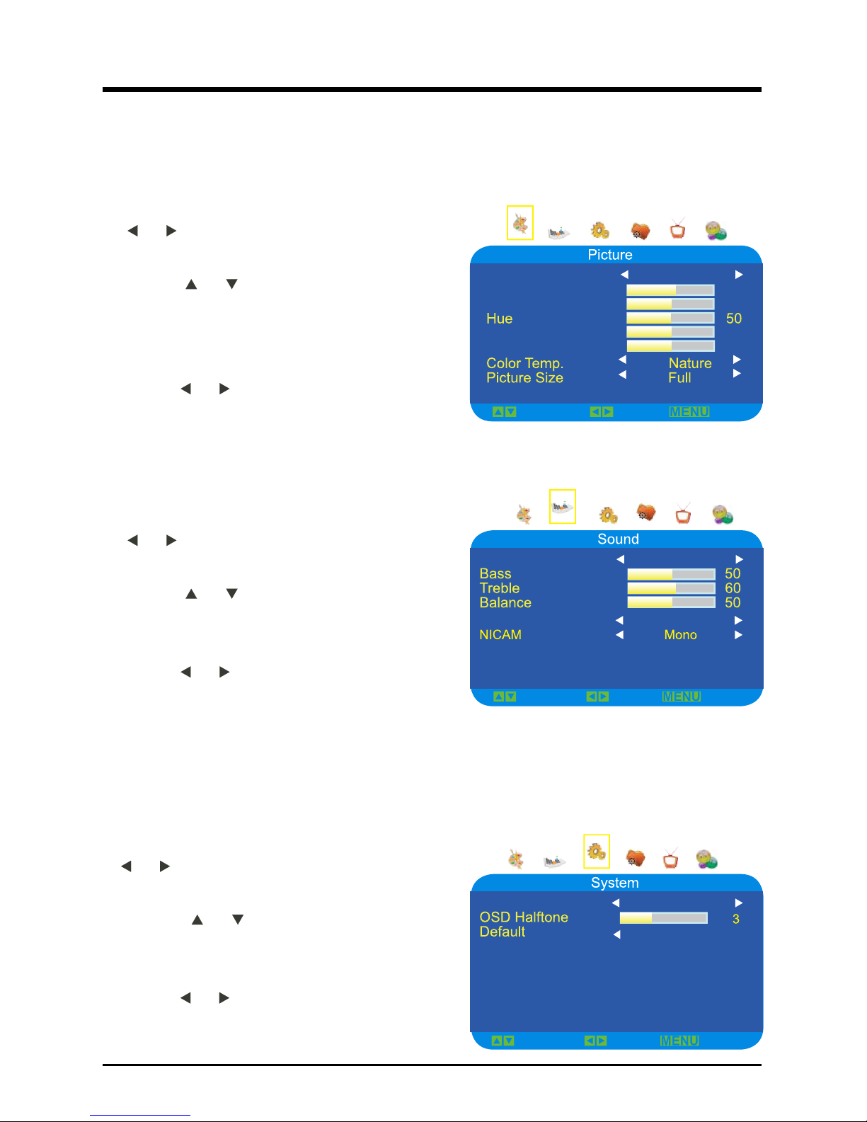
2.5.1 Picture Function
Ć
Adjustment of the Picture.
Press the Menu button, and then press
or
button until the “Picture” menu
appears.
Press or button to highlight the
“Picture Mode”,“Contrast”,“Brightness”,
“Hue”,“Saturation” “Sharpness”,“Color
Temp”,“Picture Size”item.
Press
or
button to adjust.
Press the Menu button to return or exit.
2.5.2 Sound Function
Ć
Adjustment of the Sound
Press the Menu button, and then press
or
button until the “Sound” menu
appears.
Press
or button to highlight the
“Sound Mode”, “Bass”, “Treble”,
“Balance”,“Sourround”, “NICAM” item.
Press
or
button to adjust.
Press the Menu button to return or exit.
Note: “NICAM” item is optional.
2.5.3 System Function
Ć
Adjustment of the System
Press the Menu button, and then press
or
button until the “System” menu
appears.
Press
or button to highlight the
“OSD Language”,“OSD Halftone”,
“Default” item.
Press
or
button to adjust.
Press the Menu button to return or exit.
Saturation
50
ExitSelect
Adjust
Pictuer Mode
Standard
ExitSelect
Adjust
Surround Off
OSD Language
(QJOLVK
ExitSelect
Adjust
Sharpness
50
60
Contrast
50
Brightness
Sound Mode
Standard
LCD COLOR TV
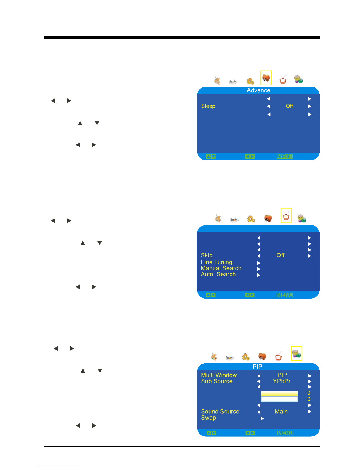
2.5.6 PIP Function
Press the Menu button, and then press
or
button until the “PIP” menu
appears.
Press or button to highlight the
“Multi Window”,“Sub Source”,“Size”,
“PIP H-Position”,“PIP V-Position”,
“Border Color”,“Sound Source”,
“Swap” item.
Press
or
button to adjust.
Press the Menu button to return or exit.
Ć
Adjustment of the PIP
2.5.5 TV Function
(Optional)
(Only for TV)
Ć
Adjustment of the TV
Press the Menu button, and then press
or
button until the “TV” menu
appears.
Press or button to highlight the
“Channel”, “Color System”, “Sound
System”, “Skip”, , “FineTuning”,
“Manual Search”, “Auto Search” item.
Press
or
button to select .
Press the Menu button to return or exit.
2.5.4 Advance Function
To control the noise reduction.
Ć
Adjustment of the Advance
Press the Menu button, and then press
or
button until the “Advance” menu
appears.
Press or button to highlight the
³'15´³6OHHS´³77;/DQJXDJH´LWHP
Press
or
button to select .
Press the Menu button to return or exit.
Note: ,QDFWLYHIRU9*$DQG'9,ĺ+'0,
77;/DQJXDJH
:(67
ExitSelect
Adjust
Channel
0
ExitSelect
Adjust
T V
PIP H-Position
ExitSelect
Adjust
PIP V-Position
3D NR
0,''/(
Color System
PAL
Sound System DK
1
Border Color
Black
Large
Size
PIP Setting23,3IXQFWLRQ;QRQ3,3IXQFWLRQ
Sub
Main
TV AV S-Video YPbPr VGA HDMI
TV ;;;OOO
AV ;;;OOO
S-Video ;;;OOO
YPbPr O O O ;;;
VGA O O O ;;;
HDMI O O O ;;;
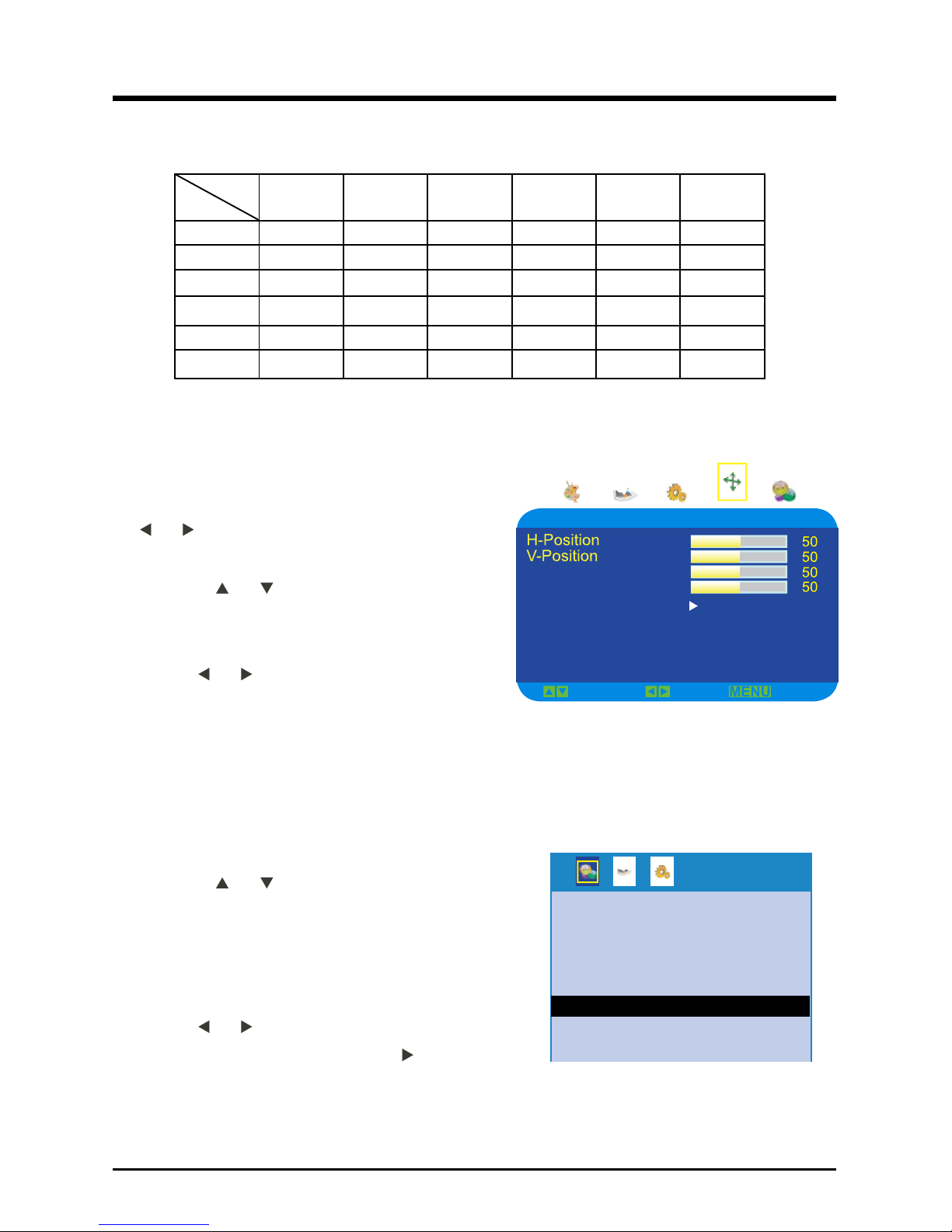
2.5.7 Geometry Function (Only for VGA )
Ć
Adjustment of the Geometry
Press the Menu button, and then press
or
button until the “Geometry”
menu appears.
Press or button to highlight the
“H-Position”,“V-Position”,“Clock”,
“Phase”, “Auto” item.
Press
or
button to adjust.
Press the Menu button to return or exit.
Geometry
Phase
Clock
Auto
ExitSelect Adjust
2.5.8 MEDIA Function (Option )
In0(',$6RXUFHWKH0(',$0(18ZLOO
always appear as right.
Press or button to select
-3(*03RU'(9,&(IXQFWLRQ7KH
-3(*RQO\VXSSRUWMSJIRUPDWGDWD03
only support.mp3 format data the device
only support FAT32 format hard disk.
Press
or
button to highlight the
-3(*RU03¿OHWKHSUHVVEXWWRQWR
play music or decording picture.
Press the Menu button to return or exit.
Ć
$GMXVWPHQWRIWKH0(',$
-3(*

LCD COLOR TV
2.6 Using the Teletext Function (Optional)
Note: When pressing the Teletext function keys on the remote control, if the
word “NO TTX” is displayed onscreen, it means the related function
can’t be used.
Teletext is a free service broadcast by most TV stations which give up-to-theminute information news,weather,television programs, share price,subtitles,and
many other topics.
7RRSHUDWH7(/(7(;7
Ć
Select a TV station on which Teletext is being transmitted.
Ć
Press the Text button once to bring up the teletext screen.Two page
QXPEHUVDUHGLVSOD\HGRQWKHVFUHHQKHDGOLQH7KH¿UVWSDJHQXPEHU
indicates your selection,while the second shows the current page
displayed.
Teletext Page Selection
Ć
(QWHUWKHUHTXLUHG7HOHWH[WSDJHDVDWKUHHGLJLWQXPEHUV7KHVHOHFWHG
page number is displayed at the top left corner of the screen. The
Teletext page counter searches until the selected page number is
located,so that the desired page is displayed on the screen.
Ć
The , buttons can be used to select the preceding or following page.
Ć
)DVW¿QGXVLQJWKH4 coloured buttons.Four subject-headed pages
FDQEHVHOHFWHGTXLFNO\E\SUHVVLQJWKHFRUUHVSRQGLQJFRORXUHGEXWWRQV
Red,Green,Yellow,or Blue on the remote control.
Useful features for Teletext
Mix
Ć
Press repeatedly to turn on Teletext Teletext blending with TV program
Teletext mode.
Index
Ć
Press this button to select the index page that displays the list of teletext
contents.

Hold
Ć
The teletext page you have selected may contain more information than
is on the screen;The rest of the information will be displayed after a
period of time on a sub page.
Ć
Press Hold button to stop the automatic page change.The hold symbol
will be displayed at the top left-hand corner on the screen and the
automatic page change will be stopped.
Ć
Press Hold button again to continue.
Reveal
Ć
Press this button once to display concealed information,such as solutions
RIULGGOHVSX]]OHVRUDTXL]
Ć
Press this button again to conceal the revealed answers.
Size
Ć
Press repeatedly to double the character size in the following order:Upper
half of the page, Lower half of the page, Return to normal size.
Page
Ć
Press this button to enter the sub page mode.You can use , button
to display sub page; Press again to exit.
CE
Ć
Press to hide teletext contents, press again to reappear.
List
Ć
Press this button to list mode, press again to exit.
LCD COLOR TV
7HFKQLFDO6SHFL¿FDWLRQ
Product Model L32K6
L37K6 L42K6
Screen Size 32” diagonal 37” diagonal 42” diagonal
Aspect Ratio 16:9
Power Supply AC 100-240V~ , 50/60 Hz
Power
Consumption
140 W
200 W 280 W
TV System 3$/%*'.,6(&$0%*'.
Audio Output
Power
,QWHUQDO
6W x 2
6W x 2 8W x 2
Input Terminal $QWHQQD,QSXW',17\SH[
9*$'6XE3LQ7\SH[
+'0,9HU&RQQHFWRU[
S-Video Input Mini Din 4 Pin Terminals x 1
Video Input RCA Terminals x 3
Component Video - YPbPr x 2 RCA Terminals
Stereo Audio x 3RCA,x 1( Phone Jack for VGA/DVI)
0(',$86%7\SH[
Output
Terminal
VHWRI$XGLR2XWSXW7HUPLQDOV5&$/5
1 set of Video Output RCA Terminals
1 set of S/PDIF Output RCA Terminals
Outline Size
/[:[+PP
without stand
with stand
799x88x529
799x236x564
914x93x595
914x236x634
1022x93x657
1022x256x712
Gross Weight 15.2Kg 19.2kg 22.5kg
Working
Temperature
0ć~40ć
Working
Humidity
20% ~ 80% Non-condensing
- When the signal received by the Display exceeds the allowed range, a
warning message will appear on the screen.
<RXFDQFRQ¿UPWKHLQSXWVLJQDOIRUPDWRQVFUHHQ
4. Supported Signal Modes
Resolution
Horizontal
)UHTXHQF\
.+]
Vertical
)UHTXHQF\
+]
640 x 480 31.50 60.00
800 x 600
35.16 56.25
37.90 60.00
1024 x 768 48.40 60.00
Resolution
Horizontal
)UHTXHQF\
.+]
Vertical
)UHTXHQF\
+]
480p
31.468
59.94
576p
31.25
50.00
720P
45.00
60.00
1080i
33.75
60.00
3[
67.50
60.00
B. YPbPr Mode
C. HDMI Mode
Note: HDMI mode can't be applied to PC function.
Note: 1. When in VGA mode, you’d better choose the resolution of 1024 x 768.
2. You’re suggested to use the VGA connecting cord of not more than 5
meters to ensure the appropriate picture quality.
Resolution
Horizontal
)UHTXHQF\
.+]
Vertical
)UHTXHQF\
+]
480i 15.734 59.94
S[ 31.468 59.94
576i 15.625 50.00
S[ 31.25 50.00
S[
37.50 50.00
45.00 60.00
1080i
28.13 50.00
33.75 60.00
3[
67.50 60.00
56.25 50.00
A. VGA Mode
AV VIDEO
S-Video
AV1 Audio
VGA
HDMI 1/2
COMP-V 1
COMP-V 2
AV2 Audio
COMP-V1 L
Audio OUT
R
AC POWER IN
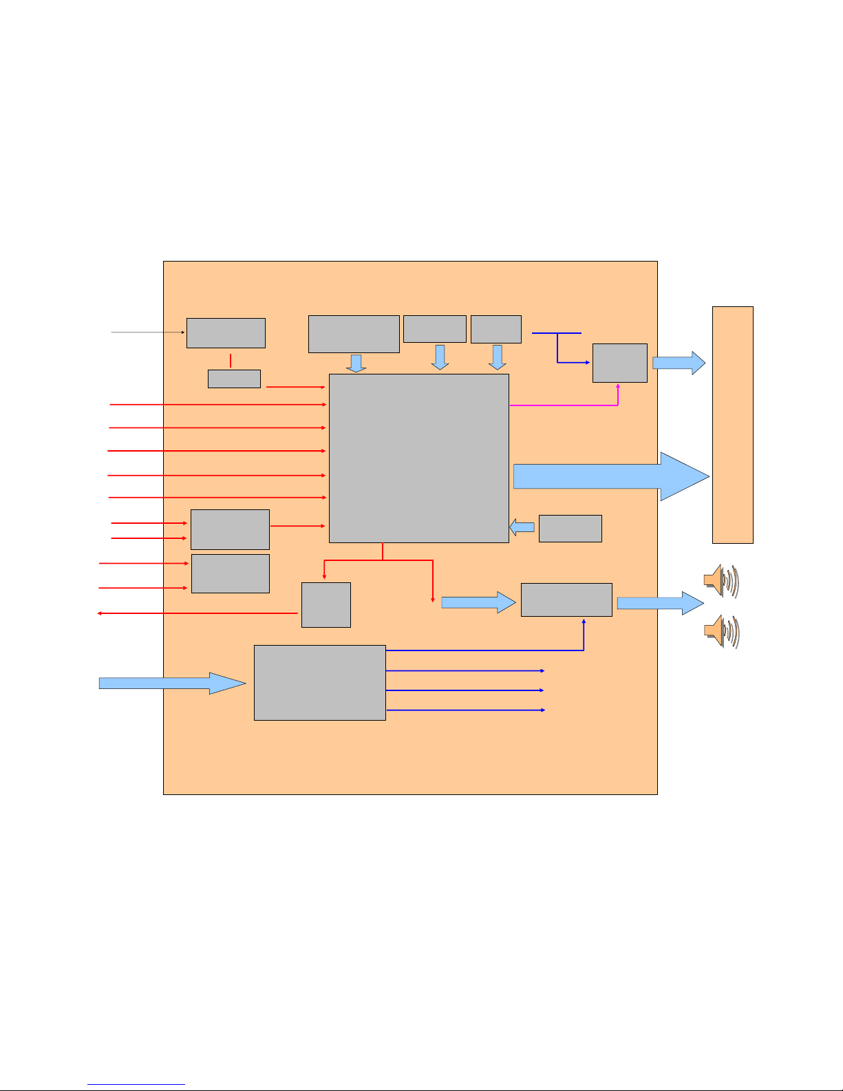
Simplified Functional Block Diagram
Mstar-6E16GS Chassis
TV IF
W
DC-DC POWER
UZ1084 3.3V
UZ1084 1.26V/2.5V
AUDIO AMPLIFIER
TDA8944J
SAWFILER
YPbPr SWITCH
PI5V330Q
AV AUDIO SWITCH
UTC4052
TUNER
ET-5C511-BS1A
PANELPower
Switch
AP2309
PANEL
LVDS SIGNAL
SIF/PIF
FLASH RAM
W25VF032
EEPROM
AT24C64
CONTROL SIGNAL
PANEL VDD
AUDIO
BUFFER
SCALER
Mstar6E16GS
SMPS(PSU)PCB Ass'y
HDZ1804-3A
DC 5V For System VSS
DC 12V For System VSS
DC 24V For Inverter VSS
DC 12V For AUDIO AMP
DDR RAM
128M-4ns
1
1
2
2
3
3
4
4
D D
C C
B B
A A
Title
Number RevisionSize
A4
D ate: 2009-5- 22 She et of
File: E:\
䆒䅵ᮍḜ
\MST6M16_FILE\Scaler.SCHDOCDraw n By:
MST6E16PROJECT - SCALER
PAGE 1 / 8 REV1.0
MST6E16
FANGDW
VI_VGA_GIN+
VI_VGA_GIN-
VI_VGA_RIN+
VI_SW _ BIN +
VI_SW _ GIN +
VI_SW _ SOG
VI_H1_CL K-
VI_H1_CL K+
GND
VI_H1_TX0-
P_3.3V_AVDD
VI_H1_TX2+
VI_H1_TX2-
VI_H1_TX1+
VI_H1_TX0+
P_3.3V_AVDD
VI_H1_TX1-
REF_HDMI
IIC_SDA_ H1
IIC_SCL_ H1
VI_VGA_HS
VI_VGA_VS
REF_SCALER
RE F_ ADC _P
RE F_ ADC _N
VI_VGA_BIN+
VI_VGA_BIN-
VI_VGA_SOG
VI_SW _ RI N+
P_3.3V_AVDD
GND
SW_SC2_FB
VI_AV1_Vin+
VI_AV2_Vin+
VI_S1 _ Cin
VI_S1 _ Yin
VI_AV3_Vin
VI_TV _ VI F+
VI_TV _ VI F-
VI_CVBS2_Out
GND
P_3.3V_SIF
AU_TV _SI F+
AU_TV _SI F-
GND
REF_AU_P
REF_AU
P_3.3V_AU
AU_VGA_ L
AU_VGA_ R
AU_MUX_ L
AU_MUX_ R
AU_GND
SW_TV_AGC
AU_Out_L1
AU_Out_R1
AU_Out_L2
AU_Out_R2
P_3.3V_VDDP
AU_SPDIF_O
SW_MUTE_M
SW_4052 _2
SW_4052 _1
GND
P_2.5V_MEM
SW_LED
SW_SC1_FS
VI_U SB_ D +
VI_U SB_ D -
P_3.3V_VDDP
SPI _CK
SPI _DI
SPI _CZ
SPI _DO
RE F_ DDR
SW_USB_DET
IIC_SDA_ M
IIC_SCL_ M
IIC_SDA_ VGA
IIC_SCL_ VGA
VI_TV_IR
P_3.3V_VDDP
SW_WP_FSH
SW _WP _M
SW_5V_PANEL
SW_H1_HPD
SW_LCD_BLK
P_3.3V_ VDDP
P_3.3V_ VDDP
GND
P_3.3V_ VDDP
SW_RESET
SW_5V_USB
SW_LCD_ADJ
SW_TV_SIF
SW_P_S TB
RE F_ USB
VI_LV_RE0+
VI_LV_RE0VI_LV_RD0+
VI_LV_RD0VI_LV_CK0+
VI_LV_CK0-
VI_LV_RC0VI_LV_RB0+
VI_LV_RB0VI_LV_RA0+
VI_LV_RA0-
VI_LV_RB1+
VI_LV_RB1VI_LV_RA1+
VI_LV_RA1-
VI_LV_RE1+
VI_LV_RE1VI_LV_RD1+
VI_LV_RD1VI_LV_CK1+
VI_LV_CK1VI_LV_RC1+
VI_LV_RC1-
MST6E16G-LF
MST6E16G-LF
RXACKN
RXACKP
RXA0N
RXA0P
AVDD _3 3
RXA1N
RXA1P
RXA2N
RXA2P
HOTPLUGA
REXT
DDCDA_SDA
DDCDA_SCA
VCLAMP
REFP
REFM
BIN1P
SOGIN1
GIN1P
RIN1P
BIN0M
BIN0P
GIN0M
GIN0P
SOGIN0
RIN0P
AVDD _3 3
GND
HSYNC0
VSYNC0
VSYNC2Y0CVBS3
CVBS2
CVBS1
VCOM1
CVBS0
VCOM0
AVDD _3 3
CVBSOUT1
CVBSOUT0
GND
XOUT
XIN
AVDD _MPL L
GND_VIFPLL
VR27
AVDD _RXS
GND_ RXS
SIFP
SIFM
VIFM
VIFP
AVDD _RXV
TAGC
AVDD_33
GND
AUVRM
AUVRP
AUVAG
AVDD_AU
LINE_IN_0L
LINE_IN_0R
LINE_IN_1L
LINE_IN_0R
AUCOM
LINE_OUR_3L
LINE_OUT_3R
LINE_OUT_2L
LINE_OUT_2R
LINE_OUT_1L
LINE_OUT_1R
GPIOD[0]
GPIOD[1]
GPIOD[2]
VDDP
GND
VDDC
AD[0]
AD[1]
AD[2]
AD[3]
WRZ
RDZ
ALE
BADR[1]
BADR[0]
RASZ
VDDC
GND
AVDD_MI
CASZ
WEZ
MADR[11]
MADR[10]
MADR[9]
MADR[8]
MADR[7]
MADR[6]
MADR[5]
MADR[4]
MADR[3]
MADR[2]
MADR[1]
MADR[0]
GND
AVDD_MI
AVDD_MIPLL
DQM0
DQS0
AVDD _MI
MDATA[0]
MDATA[1]
GND
MDATA[2]
MDATA[3]
AVDD _MI
MDATA[4]
MDATA[5]
MDATA[6]
MDATA[7]
AVDD _MI
MDATA[8]
MDATA[9]
GND
MDATA[10]
MDATA[11]
AVDD _MI
MDATA[12]
MDATA[13]
MDATA[14]
MDATA[15]
AVDD _MI
DQS1
DQM1
MCLKZ
MCLK
MCLKE
MVREF
USB20_REXT
AVDD _USB
USB20_DM
USB20_DP
GND
VDDP
SPI_SCK
SPI_SDI
SPI_SCZ
SPI_SDO
GND
VDDC
SAR0
SAR1
SAR2
SAR3
PWM0
PWM1
DDCR_SDA
DDCR_SCL
DDCA_SDA
DDCA_SCL
INT
IRIN
VDDP
PWM2
PWM3
VDDP
GPIOT[1]
HWRESET
GND
VDDC
LVA4P
LVA4M
LVA3P
LVA3M
LVACKP
LVACKM
LVA2P
LVA2M
LVA1P
LVA1M
LVA0P
LVA0M
VDDP
GND
LVB4P
LVB4M
LVB3P
LVB3M
LVBCKP
LVBCKM
LVB2P
LVB2M
LVB1P
LVB1M
LVB0P
LVB0M
VDDP
GND
GPIOM[0]
GPIOM[1]
VDDC
RXBCKN
RXBCKP
AVDD_33
RXB0N
RXB0P
GND
123456789101112131415161718192021222324252627282930313233343536373839404142434445464748495051
52
53
54
55
56
57
58
59
60
61
62
63
64
65
66
67
68
69
70
71
72
73
74
75
76
77
78
79
80
81
82
83
84
85
86
87
88
89
90
91
92
93
94
95
96
97
98
99
100
101
102
103
104
156
155
154
153
152
151
150
149
148
147
146
145
144
143
142
141
140
139
138
137
136
135
134
133
132
131
130
129
128
127
126
125
124
123
122
121
120
119
118
117
116
115
114
113
112
111
110
109
108
107
106
105
208
207
206
205
204
203
202
201
200
199
198
197
196
195
194
193
192
191
190
189
188
187
186
185
184
183
182
181
180
179
178
177
176
175
174
173
172
171
170
169
168
167
166
165
164
163
162
161
160
159
158
157
RXB1N
RXB1P
GND
RXB2N
RXB2P
HPLUGB
DDCDB_SDA
DDCDB_SCL
216
215
214
213
212
211
210
209
MST6E16GS-LF
U103
VI_AV2_Vin-
VI_AV1_Vin-
VI_CVBS1_Out
P_3.3V_VIF
X_OUT
X_IN
P_3.3V_MPLL
GND
P_3.3V_AU
AU_Out_L3
AU_Out_R3
GND
GND
GND
GND
GND
GND
GND
VI_H2_CLKVI_H2_CLK+
VI_H2_T X0-
VI_H2_T X2+
VI_H2_T X2-
VI_H2_T X1+
VI_H2_T X0+
P_3.3V_ AVDD
VI_H2_T X1-
II C_ SD A_H2
IIC_SCL_H2
SW_H2_HPD
GND
GND
P_1.2V_ C
P_1.2V_ C
P_3.3V_ AVDD
P_1.2V_C
P_1.2V_C
P_1.2V_C
RE F_ VR2 7
P_3.3V_MIPLL
P_2.5V_MEM
P_2.5V_MEM
P_2.5V_MEM
DDR_ DA TA7
DDR_ DA TA6
DDR_ DA TA5
DDR_ DA TA4
DDR_ DA TA3
DDR_ DA TA2
DDR_ DA TA1
DDR_ DA TA0
DDR_ DQS0
DDR_ LDQ M
DDR_WEZ
DDR_CASZ
DDR_RASZ
DDR_BA0
DDR_BA1
DDR_AR0
DDR_AR1
DDR_AR2
DDR_AR3
DDR_AR4
DDR_AR5
DDR_AR6
DDR_AR7
DDR_AR8
DDR_AR9
DDR_AR10
DDR_AR11
DDR_ CKE
DDR_ MCLK+
DDR_ MCLK-
DDR_ UD QM
DDR_ DQS1
DDR_ DA TA8
DDR_ DA TA9
DDR_ DA TA10
DDR_ DA TA11
DDR_ DA TA12
DDR_ DA TA13
DDR_ DA TA14
DDR_ DA TA15
P_2.5V_MEM
P_2.5V_MEM
P_2.5V_MEM
SW_SC2_FS
SW_SC1_FB
SW _TV_KEY
SW _TV_KEY1
SW _TV_KEY2
GND
GND
REF_SCALER
RE F_ ADC _P
RE F_ ADC _N
RE F_ AU_ P
RE F_ AU
RE F_ VR2 7
RE F_ DDR
RE F_ USB
910
R103
10K
R101
10K
R102
4.7uF
C110
100n
C106
100n
C107
100n
C112
100n
C109
100n/nc
C108
1uF
C114
4.7uF
C115
10uF
C116
100n
C117
1n
C104
100n
C105
GND
P_2.5V_MEM
REF_HDMI
390
R104
4.7K x 4
R148
4.7K x 4
R150
SW_TV_SIF
SW_P_STB
SW_LED
IIC_SDA_ M
IIC_SCL_ M
II C_S DA _VGA
II C_S CL_ VGA
SW_WP_FSH
SW_WP _M
SW_5V_PANEL
SW_TV_KEY
SW_TV_KEY1
SW_TV_KEY2
VI_TV _ IR
SW_LCD_BLK
SW_5V_USB
SW_LCD_ADJ
4.7K x 4
R149
4.7KR133
4.7KR134
4.7K
R135
SW_4052_2
SW_4052_1
4.7KR139
47K
R131
100K
R132
P_3.3V_A P_5Vs_SA
P_3.3V_M
P_3.3V_AVDD
GND
P_5V_USBSW _US B_DE T
VI_LV_RC0+
P_3.3V_M
4.7K x 4
R138
SW_PDP_D ISPEN
SW_MUTE_M
SW_YPbPr
SW_YPbPr
4.7KR140
P_3.3V_M
100n
C123
1
1
2
2
3
3
4
4
D D
C C
B B
A A
Title
Number RevisionSize
A4
D ate: 2009-5- 22 She et of
File: E:\
䆒䅵ᮍḜ
\..\DDR&EPROM.SCHDOC Drawn By:
MST6E16PROJECT - DDR
PAGE 2 / 8 REV1.0
MST6E16
FANGDW
MVDD1DQ02VDDQ3DQ14DQ25VSSQ6DQ37DQ48VDDQ9DQ510DQ611VSSQ12DQ713NC14VDDQ15LDQS16NC17MVDD18NC19LDM20WE21CAS22RAS23CS24NC25BA026BA127A10/AP28A029A130A231A332MVDD
33
VSS
34
A435A536A637A738A839A9
40
A11
41
NC42NC
43
CKE44CLK45CLK
46
UDM
47
VSS
48
VREF
49
NC
50
UDQS
51
VSSQ
52
NC
53
DQ8
54
VDDQ
55
DQ9
56
DQ10
57
VSSQ
58
DQ1159DQ12
60
VDDQ
61
DQ1362DQ14
63
VSSQ
64
DQ15
65
VSS
66
HY 5DU281622ET-4
U102
100X4
R105
100X4
R107
100X4
R106
100X4
R108
22X4
R146
22X4R147
22X4R145
22X4
R144
100
R125
100
R127
33X4R143
100R123
10KR124
100R128
150R130
10KR126
1nFC111
0.1uFC113
GND
GND
GND
DDR_ DA TA7
DDR_ DA TA6
DDR_ DA TA5
DDR_ DA TA4
DDR_ DA TA3
DDR_ DA TA2
DDR_ DA TA1
DDR_ DA TA0
DDR_ DQS0
DDR_ LDQ M
DDR_ WEZ
DDR_ CA SZ
DDR_ RA SZ
DDR_ BA0
DDR_ BA1
DDR_ AR 0
DDR_ AR 1
DDR_ AR 2
DDR_ AR 3 DDR_ AR 4
DDR_ AR 5
DDR_ AR 6
DDR_ AR 7
DDR_ AR 8
DDR_ AR 9
DDR_ AR 10
DDR_ AR 11
DDR_ CKE
DDR_ MCLK+
DDR_ MCLK-
DDR_ UD QM
DDR_ DQS1
DDR_ DA TA8
DDR_ DA TA9
DDR_ DA TA10
DDR_ DA TA11
DDR_ DA TA12
DDR_ DA TA13
DDR_ DA TA14
DDR_ DA TA15
P_2.5V_DMC
P_2.5V_DMQ
CE1SU2WP3GND
4
SI
5
SCK
6
HOLD
7
VCC
8
PMC2 5L080
U101
1nF
C122
100uF
C118
1uF
C121
BAV99
D101
N3906
Q101
10K
R151
1K
R153
10K
R152
1K
R121
1 2
14.318M
Y101
27p
C119
27p
C120
1M
R154
GND
GND
GND
100n
C101
100
R112
100n
R109
GND
NC1E12E23GND
4
SDA5SCL
6
WP
7
VCC
8
24C04_SO8
U105
100
R114
100
R115
0
R113
4.7K
R141
100n
C102
15
CN5/PH2.0
CN101
4.7K/NC
R110
IIC_SDA_ M
IIC_SCL_ M
P_5Vs_SA
GND
GND
GND
NC1E12E23GND
4
SDA5SCL
6
WP
7
VCC
8
24C32_SOP8
U104
100
R117
100
R118
100
R116
4.7K
R142
100n
C103
SW_WP _M
P_5Vs_SA
GND
IIC_SDA_ M
IIC_SCL_ M
14
CN4/PH2.0
CN102
100R119
100R120
GND
X_IN
X_OUT
SW_WP _FSH
P_3.3V_A
GND
P_3.3V_A
P_5Vs_SA
IIC_S CL_ VGA'
IIC_S DA _VG A '
SW_RESET
SPI _CK
SPI _DI
SPI _CZ
SPI _DO
33X 4
R111
FB/060 3
L101
4.7K
R122
FLASH
EEPROM FOR HDCP KEY
EEPROM FOR MAIN CPU
220
R155
II C_S DA _VGA
II C_S CL_ VGA
1
1
2
2
3
3
4
4
D D
C C
B B
A A
Title
Number RevisionSize
A4
D ate: 2009-5- 22 She et of
File: E:\
䆒䅵ᮍḜ
\..\Terminal input.SCHD OC Drawn By :
MST6E16PROJECT - TERMINAL1
PAGE 3 / 8 REV1.0
MST6E16
FANGDW
10R450
10R446
10R447
10R449
GND
10R442
10R435
10R438
10R439
100R452
100R451
4.7K
R455
4.7K
R454
4.7K
R456
1K
R459
VI_H1_TX2+
VI_H1_TX2-
VI_H1_TX1+
VI_H1_TX1-
VI_H1_TX0+
VI_H1_TX0-
VI_H1_CLK+
VI_H1_CLK-
SW_H1_HPD
P_5V_SC
IIC_SCL_ H1
IIC_SDA _H 1
0.15p
D422
0.15p
D421
0.15p
D423
0.15p
D425
0.15p
D427
10pF
D429
0.15p
D424
0.15p
D426
0.15p
D428
10pF
D430
10pF
D431
N3904
Q402
GND
1
19
HPD
+5V HDMI
DDC SDA
GND
DDC SCLNCCEC
CLK-
GND
CLK+
TX0-
GND
TX0+
TX1-
GND
TX1+
TX2-
GND
TX2+
212022
23
HDMI
J404
GND
HDMI EDID
HDMI INPU T
10R421
10R417
10R418
10R420
GND
10R412
10R407
10R408
10R411
100R425
100R423
4.7K
R427
4.7K
R426
4.7K
R430
1K
R432
VI_H2_TX2+
VI_H2_TX2-
VI_H2_TX1+
VI_H2_TX1-
VI_H2_TX0+
VI_H2_TX0-
VI_H2_CLK+
VI_H2_CLK-
SW_H2_HPD
P_5V_SC
IIC_SCL_ H2
IIC_SDA _H 2
0.15p
D408
0.15p
D407
0.15p
D409
0.15p
D411
0.15p
D413
10pF
D415
0.15p
D410
0.15p
D412
0.15p
D414
10pF
D416
10pF
D419
N3904
Q401
GND
1
19
HPD
+5V HDMI
DDC SDA
GND
DDC SCLNCCEC
CLK-
GND
CLK+
TX0-
GND
TX0+
TX1-
GND
TX1+
TX2-
GND
TX2+
212022
23
HDMI
J403
GND
HDMI EDID
HDMI INPU T
1nF
C423
1nF
C421
1nF
C420
FB/060 3
L405
FB/060 3L406
FB/060 3
L404
100K
R445
100K
R440
75
R457
GND
4.7KR448
1K
R4361KR433
GND
15K
R441
100p
C417
BLUE
GREEN
RED/C
SWITCH
BLANK
AU_Y1_R'
AU_Y1_L'
SW_SC2_FS
SW_SC2_FB
VI_SC2_Out
VI_Y2_P r'
AOR
1
AIR
2
AOL
3
Gnd4Gnd5AIL
6
B
7
SWITCH
8
Gnd
9
CLK
10
G
11
DATA
12
Gnd13Gnd
14
R/C
15
BLANK
16
Vo_G
17
Vi_Gnd
18
Vout
19
VIN
20
SHIELD
21
SCART2
J402
10p
D432
VI_Y1_P b'
VI_Y1_Y'
VI_Y1_P r'
560p
C405
560p
C404
1nF
C413
1nF
C407
1nF
C406
100p
C414
FB/060 3
L402
FB/060 3L403
FB/060 3
L401
10K
R413
10K
R414
10K
R406
100K
R415
100K
R409
75
R431
75
R429
GND
10K
R404
4.7KR416
1K
R4051KR403
GND
15K
R410
100p
C403
BLUE
GREEN
RED/C
SWITCH
BLANK
AU_AV1_R
AU_AV1_L
SW_SC1_FS
SW_SC1_FB
VI_SC1_Out
VI_AV1_Vin+
VI_AV1_Vin-
AOR
1
AIR
2
AOL
3
Gnd4Gnd5AIL
6
B
7
SWITCH
8
Gnd
9
CLK
10
G
11
DATA
12
Gnd13Gnd
14
R/C
15
BLANK
16
Vo_G
17
Vi_Gnd
18
Vout
19
VIN
20
SHIELD
21
SCART1
J401
10pF
D420
10p
D418
2.2uF
C402
2.2uF
C401
VI_SC1_CVBS'
AU_SC1_L'
AU_SC1_R'
AU_SC1_R'out
AU_SC1_L'ou t
47nF
C410
47nF
C409
75
R42275R424
100R366
47nFC324
VI_AV2_Vin-
GND
GND
GND
VI_S1 _Cin'
2.2uF
C307
2.2uF
C302
C304
C310
AU_Out_ L 3
AU_Out_ R3
2.2uF
C325
2.2uF
C316
1nF
C319
1nF
C328
AU_Out_ L 2
AU_Out_ R2
BAT54C
D401
BAT54C
D403
1
1
2
2
3
3
4
4
D D
C C
B B
A A
Title
Number RevisionSize
A4
D ate: 2009-5- 22 She et of
File: E:\
䆒䅵ᮍḜ
\..\Terminal input2.SCHD OC Draw n By:
MST6E16PROJECT - TERMINAL2
PAGE 4 / 8 REV1.0
MST6E16
FANGDW
47
R458
VI_Y2_P r'
GND
5p
C455
5p
C457
5p
C456
75
R491
75
R490
75
R489
GND
0
R4860R485
0
R482
2.2uF
C447
2.2uF
C450
2.2uF
C452
GND
10p
D446
10p
D445
10p
D444
VI_Y2_Y
VI_Y2_P b
VI_Y2_P r
GN D
Y1
Y2
GN D
Pb1
Pb2
GN D
Pr1
Pr2
J405A
GN D
Y1
Y2
GN D
Pb1
Pb2
GN D
Pr1
Pr2
J405B
VI_Y2_P r'
16
CN6/PH2.0
CN402
GND
GND
GND
VI_SC1_Out
AU_S C1_ R 'o ut
AU_S C1_ L' ou t
GN D
V in
V out
GN D
L in
Lout
GN D
R in
R out
AV6 VID EO L/R Y/R/ W
J406A
GND
VI_SC1_CVBS'
GND
AU_SC1_L'
GND
AU_SC1_R'
GN D
V in
V out
GN D
L in
Lout
GN D
R in
R out
J406B
AU_SC1_R'out
AU_SC1_L'ou t
VI_SC1_Out
V IDEO I N/O UT
17
CN301
100p
C323
560p
C331
560p
C330
10K
R374
10K
R373
75
R365
GND
10KR368
10KR372
47R362
L
R
10p
D302
VI_A V3_ V in
AU_AV3_L
AU_AV3_R
2.2uF
C327
2.2uF
C329
47nFC321
GND
100p/NC
C336
100p/NC
C337
75
R382
75
R381
GND
47
R37847R377
10p
D303
10p
D304
VI_S1 _Yin
47nF
C335
47nF
C333
VI_S1 _Cin
10p
D301
FB/060 3
L301
75R357
100
R361
100n
C318
1nF/NC
C320
AU_SPDIF_O
5pC451
1nF/NC
C429
5pC449
5pC445
75R484
4.7K
R466
75R480
75R475
100p/NC
C430
FB/060 3L408
FB/060 3L407
FB/060 3L410
47nFC444
47nFC448
47nFC441
47nFC446
100R472
47R474
47R478
390R479
47R481
4.7K
R465
100n
C427
GND
47R483
1nFC442
GND
100
R473
47nFC436
VI_VGA_VS
VI_VGA_HS
VI_VGA_BIN-
VI_VGA_BIN+
VI_VGA_SOG
VI_VGA_GIN+
VI_VGA_GIN-
VI_VGA_RIN+
0.15p
D441
0.15p
D442
0.15p
D443
5pC440
5pC437
5pC443
10p
D434
10p
D435
10p
D436
10p
D437
560p
C460
560p
C459
10K
R493
10K
R492
10KR487
10KR488
L
R
AU_V GA_L
AU_V GA_R
2.2uF
C453
2.2uF
C454
GND
P_5V_SC
2/R
4/L
He adphone
J410
1
6
11
5
10
15
SCL
GN D
GN D
VSYNC
MRXD
+5V
HSY NCBGN D
SDAGGN D
MTXDRGN D
16 17
VGA
J408
100R401
100R402
VG A AUD I O INP UT
1K
R463
1K
R464
II C_S CL_ VGA'
II C_S DA _VGA '
560p
C439
560p
C438
10K
R477
10K
R476
10KR470
10KR471
GND
L
R
AU_Y1_L'
AU_Y1_R'
AU_Y1_L
AU_Y1_R
2.2uF
C434
2.2uF
C435
GN D
L1
L2
GN D
R1
R2
AUDIO L/R X2
J409A
YPbPr INPUT
560p
C464
560p
C463
10K
R497
10K
R496
10KR494
10KR495
GND
L
R
AU_Y2_L
AU_Y2_R
2.2uF
C458
2.2uF
C461
2.2uF
C462
FB/060 3
L409
AU_GND
GN D
L1
L2
GN D
R1
R2
AUDIO L/R X2
J409B
5p
C431
5p
C433
5p
C432
75
R469
75
R468
75
R467
0R462
0R461
0R460
2.2uF
C425
2.2uF
C426
2.2uF
C428
10p
D438
10p
D439
10p
D440
VI_Y 1_ Y'
VI_Y 1_ Pb'
VI_Y1_P r'
VI_Y1_Y
VI_Y1_P b
VI_Y1_P r
VI_AV3_Vin'
47R499
2.2uF
C422
VI_A V2_ V in +
VI_S1 _ Cin'
6
C
Y
SPDIF
42789
S_VIDEO&SPDIF
J301
BAT54C
D405
1
1
2
2
3
3
4
4
D D
C C
B B
A A
Title
Number RevisionSize
A4
D ate: 2009-5- 22 She et of
File: E:\
䆒䅵ᮍḜ
\MST6M16_FILE\switch.SCHDOCDraw n By:
MST6E16 PR OJECT - SWITCHING
PAGE 5 / 8 REV1.0
MST6 E16
FANGDW
GND
GND
100K
R320
100K
R323
100K
R321
100K
R336
100K
R337
100K
R338
Y
Pb
Pr
IN
1
S1A2S2A
3
DA
4
S1B5S2B
6
DB
7
GND
8
DC
9
S2C10S1C
11
DD
12
S2D13S1D
14
EN15VCC
16
PI5 V330
U301
100K
R319
100K
R318
100K
R322
100K
R333
100K
R334
100K
R335
0
R3280R3290R331
VI_Y 1_ Y
VI_Y 1_ Pb
VI_Y 1_ Pr
VI_Y 2_ Y
VI_Y 2_ Pb
VI_Y 2_ Pr
VI_Y1_Y
VI_Y1_P b
VI_Y1_P r
100n
C301
Y22Y01Y3Y3
4
VCC
16
Y15EN
6
X
13
VEE7GND
8
X0
12
B9A
10
X3
11
X215X1
14
74HC 40 52
U302
SW_YPbPr
SW_4052_2
YPbPr1/YPbPr2 SWITCHING
VI_SW _BIN +
VI_SW _GIN +
VI_SW _SOG
VI_SW _ RI N+
47
R33947R341
390
R345
47nF
C309
47nF
C306
47nF
C339
47
R346
47nF
C340
100K x 4
R386
100K x 4
R388
100K x 4
R387
100K x 4
R389
AU_Y1_R
AU_AV3_R
AU_MUX_R
AU_AV1_R
AU_Y2_R
AU_AV3_L
AU_Y2_L
AU_MUX_L
AU_Y1_L
AU_AV1_L
2.2uF
C315
2.2uF
C313
GND
GND
SW_4052_1
P_5V_SC
FB/0 603
L302
N3904
Q304
N3904
Q303
N3904
Q305
N3906
Q301
100n
C311
2.2uF
C312
100uF
C342
100
R343
100
R317
0
R350
100K
R353
100K
R347
100K
R351
4.7K
R348
75
R349
47
R352
GND
GND
1nF
C314
VI_C VBS 2 _O ut
VI_SC2_Out
P_5V_SC
*
*
*
4.7K
R314
4.7K
R330
N3904
Q308
N3906
Q302
2.2uF
C332
2.2uF
C334
100uF
C343
10
R380
100K
R385
100K
R375
47K
R383
470
R376
75
R379
75
R384
GND
GND
1nF
C338
VI_C VBS 1 _O ut
VI_SC1_Out
P_5V_Vcc
R317: 33K
R315: 56
R314: 220
FOR MST 9E19B
*
*
*
GNDGND
GND GND
5
7
4
123
6
8
GND_ PAD_HALF
GND301
5
7
4
123
6
8
GND_ PAD_HALF
GND302
5
7
4
123
6
8
GND_ PAD_HALF
GND303
5
7
4
123
6
8
GND_ PAD_HALF
GND304
SW1
SW2
0
0
0
1
1
0
1
1
AV3
AV1AV 3'
YPbPr1 YPbPr2
AV2
100
R315
1K
R316
100n
C305
22uF
C308
GND
P_12V_DTV
P_12V_DTV
P_12V_DTV
10K
R325
10K
R332
1K
R313
1
1
2
2
3
3
4
4
D D
C C
B B
A A
Title
Number RevisionSize
A4
D ate: 2009-5- 22 She et of
File: E:\
䆒䅵ᮍḜ
\..\Signal power.SCHDOC Draw n By:
MST6 E16PROJ E CT - CONNECTER
PAGE 6 / 8 REV1.0
MST6E16
FANGDW
1K
R513
12V
12V
GND
GND
5Vcc
5Vcc
GND
GND
RELAY
5Vsb
STB
N3904
Q502
100R515
4.7K
R514
P_5Vs_St b
100uF
C559
100uF
C582
100uF
C566
100n
C584
100n
C545
100n
C583
GND
GND
GND
GND
P_5V_Vcc
P_12V_M
111
CN11/PH2.5
CN504
IN
3
1
OUT
GND
2,4
AZ1084U501
IN
3
1
OUT
GND
2,4
AZ1084SU503
100uF
C558
100n
C531
100n
C532
100n
C533
100n
C534
100n
C535
100n
C536
100n
C537
100n
C574
100n
C575
100n
C538
100n
C539
FB/0 603
L514
1uF
C562
1uF
C561
100n
C511
FB/080 5
L524
GND
GND
P_2.5V_MEM
SW_P_STB
FB/060 3
L502
1uF
C568
GND
FB/060 3
L505
100n
C513
100uF
C557
100n
C512
GND
P_5Vs_SA
P_5V_SC
100n
C509
FB/080 5
L521
100n
C565
1uF
C580
GND
P_VCC_L CD
1uF
C564
100n
C546
GND
P_12V_DTV
FB/060 3
L516
470
R503
510
R504
GND
SW_PDP_BR I
100uF
C556
GND
L521
L524
AUO/CMO LG/HITACHI
XO
OX
+12V
+5V
IN
3
1
OUT
GND
2,4
AZ1084SU502
100uF
C560
100n
C547
100n
C548
100n
C549
100n
C550
100n
C551
100n
C552
100n
C553
100n
C578
100n
C579
100n
C554
100n
C555
FB/0 603
L518
FB/060 3L517
1uF
C563
GND
P_1.2V_C
10K
R505
100
R506
GND GND
*
470uF
C581
100n
C502
100n
C503
100n
C504
100n
C505
100n
C506
2.2uF
C567
100n
C508
100n
C523
2.2uF
C518
100n
C501
100n
C516
100n
C519
FB/060 3L504
100n
C514
100n
C515
FB/060 3
L506
100n
C522
100n
C517
2.2uF
C570
100n
C520
100n
C510
2.2uF
C524
FB/060 3
L512
2.2uF
C573
100n
C525
FB/060 3
L508
100n
C507
GNDGND
GND
P_3.3V_VDDP
P_3.3V_AU
P_3.3V_SIF
P_3.3V_AVDD
P_3.3V_A P_3.3V_VIF
300
R501
510
R502
FB/060 3
L507
FB/0 603
L511
GND
GND GND
P_3.3V_MI PLL
100n
C521
2.2uF
C571
FB/060 3
L509
GND
P_3.3V_MPLL
100n
C540
100n
C541
100n
C542
100n
C543
100n
C544
100n
C576
100n
C577
P_2.5V_DMQ
GND
100n
C526
100n
C527
100n
C528
100n
C529
100n
C530
P_2.5V_DMC
GND
FB/060 3
L515
FB/060 3
L513
100n
C594
P_3.3V_M
100n
C572
GND
FB/0 603
L503
P_3.3V_M
1uF
C589
100n
C588
10KR540
10K
R539
10K
R538
4.7K
R541
4.7K
R543
GND
100n
C591
GND
ADJ
BLK
N3904
Q506
N3904
Q507
GND
FB/080 5
L529
FB/080 5L528
14
CN4/PH2.0
CN507
P_5Vs_SA
SW_LCD_ADJ
SW_LCD_BLK
FB/080 5L531
SW_PDP_BR I
1uF
C592
GND
N3904
Q505
4.7K
R535
100n
C593
GND
GND
100R526
100
R530
VI_LV _ RE0+
VI_LV _ RE0-
VI_LV _ RD 0+
VI_LV _ RD 0-
VI_LV _ CK0 +
VI_LV _ CK0 -
VI_LV _ RC 0+
VI_LV _ RC 0-
VI_LV _ RB0+
VI_LV _ RB0-
VI_LV _ RA 0+
VI_LV _ RA 0-
P_3.3V_A
P_3.3V_A
SW_PDP_DISPEN
GND
GND
GND
0/NCR532
4.7KR536
VI_LV _ RB1+
VI_LV _ RB1-
VI_LV _ RA 1+
VI_LV _ RA 1-
VI_LV _ RE1+
VI_LV _ RE1-
VI_LV _ RD 1+
VI_LV _ RD 1-
VI_LV _ CK1 +
VI_LV _ CK1 -
VI_LV _ RC 1+
VI_LV _ RC 1-
GND1GND2RA0-3RA0+4RB0-5RB0+6RC0-7RC0+8RCLK0-9RCLK0+10RD0-11RD0+12RE0-13RE0+14GND15GND16RA1-17RA1+18RB1-19RB1+
20
RC1-
21
RC1+
22
CLK1-
23
CLK1+
24
RD1-
25
RD1+
26
RE1-
27
RE1+
28
OP129OP2
30
GND31GND
32
VCC33VCC34VCC35VCC
36
GND37GND38GND39GND
40
Header 2 0X2 ACN508
4.7K
R510
4.7K
R509
1uF
C590
N3904
Q508
1K
R542
47K
R544
GND
P_VCC_L CD
IN4148
D504
1
3 2
MP5307
Q510
4.7KR545
SW_5V_PANEL
FB/080 5
L522
1uF
C587
100n
C586
1uF
C585
N3904
Q504
1K
R523
GND
P_5V_Vcc
1
3 2
MP5307
Q509
4.7K
R533
SW_5V_USB
FB/0 805
L519
P_5V_USB
16
CN6/PH2.0
CN501
10R5 07
10
R508
10pD5 02
10pD5 01
VI_USB_D+
VI_USB_D-
1.8K
R522
100R516FB/0603L523
IR
GND
RED
+5V
15
CN5/PH2.0
CN502
VI_TV _ IR
P_5Vs_SA
SW_LED
1K
R519
GND/GREEN
18
CN8
CN503
1.2K
R524
1.8K
R528
4.7KR527
1.2K
R531
10
R518
10
R525
10
R534
10
R537
FB/060 3L527
GND
10p
D505
KEY
GND
12
CN2/PH2.0
CN506
SW_TV_KEY
FB/060 3
L530
FB/060 3
L526
FB/060 3
L525
N3904
Q503
N3904
Q501
1K
R517
FB/060 3L520
1K
R520
1K
R521
GND
GND
SW_TV_KEY1
SW_TV_KEY2
100n
C595
GND
1
1
2
2
3
3
4
4
D D
C C
B B
A A
Title
Number RevisionSize
A4
D ate: 2009-5- 22 She et of
File: E:\
䆒䅵ᮍḜ
\MST6M16_FILE\TUNER1.SCHDOCDrawn By :
MST6E16PROJECT - TUNER
PAGE 7 / 8 REV1.0
MST6E16
FANGDW
IN11IN2
2
GND
3
OUT1
4
OUT2
5
K9453
SAW201
IN11IN2
2
GND
3
OUT1
4
OUT2
5
K3953
SAW202
N3904
Q201
C1674
Q203
100n
C205
100n
C210
10nF
C206
10nF
C223
10nF
C202
1nF
C208
470
R205
47uF
C222
56
R214
100
R221
100
R220
1.8K
R216
12K
R223
4.7K
R213
1uH
L203
FB/060 3
L202
IN4148
D202
GND_ TU
GND_ TU
BAS85/NCD206
BAS85/0D205
BAS85/NC
D207
100K
R207
6.8K
R203
680K
R211
6.8K
R202
22K
R209
100
R201
GND_TU
470uF
C221
GND_ TU
GND_ TU
FB/060 3
L205
GND_ TU
22K
R226
+33V
+5V
GND_TU
P_12V_DTV
100n
C204
100uF
C213
100p
C203
100n
C215
P_5V _Vcc
150R224
AGC
1
TU
2
SCL
4
SDA
5
VCC
6
BP
7
BT
9
IF
11
NC
8
GND
10
GND13GND
12
AS
3
GND
14
GND
15
TUNER
TU201
4.7K
R222
100p
C211
100p
C212
GND_TU
FB/060 3
L201
100n
C201
0
R210
56
R215
1uH
L204
GND_TU
TUNE R
SW_TV_AG C
IIC_SDA_ M
IIC_SCL_ M
2200pF
C217
100KR2 06
GND_ TU
N3904
Q202
1mH
L206
10uF
C214
ZD33V
D204
100R204
1uF
C218
1n
C219
470pF
C220
4700pF
C216
1mH
L207
GND_TU
BAV99
D201
150R225
ZD9V1
D203
56
R217
1.2K
R208
10nF
C207
100p
C209
GND_ TU
VI_TV _ VI F+
VI_TV _ VI F-
AU_TV _SI F+
AU_TV _SI F-
SW_TV_SIF
P_5V_TU
4.7K
R227
100n
C227
100n
C226
P_5V_TU
100uF
C224
FB/0 603
L208
100n
C225
P_5V_Vcc
GND

1
1
2
2
3
3
4
4
D D
C C
B B
A A
Title
Number RevisionSize
A4
D ate: 2009-5- 22 She et of
File: E:\
䆒䅵ᮍḜ
\ ..\SPEAKER_AMP.SCHDOCDr awn B y:
MST6E16 PROJECT - AUDIO AMP
PAG E 8/ 8 REV 1. 0
MST6 E16
FANGDW
220n
C607
1.5n
C611
220n
C608
220n
C609
220n
C610
1.5n
C612
1.5n
C604
1.5n
C605
10uF
C619
470uF
C618
1000uF
C620
47nF
C613
2.2uF
C603
2.2uF
C602
10K
R609
10K
R610
N3904
Q603
10k
R616
1K
R615
N3904
Q604
1K
R619
10K
R617
1KR607
1KR608
GND_AMP
GND
GND
100n
C606
100n
C615
100mHL603
GND_AMP GND_AMP
AU_Out_ L 1
AU_Out_ R1
P_5V_Vcc
47nF
C614
100n
C616
L-R-R+
L+
1K
R620
10K
R621
N3906
Q605
1u
100p
C623
100n
C617
220uF/25V
C621
BAV99
D603
GND
GND
1uF
C622
15K
R618
4.7K
R614
GND_AMP
10k
R612
10k
R613
16
CN6/PH2.5
CN602
P_18V_AMP
100
R601
100
R602
FB/060 3
L601
FB/060 3
L602
MUTE O N/OF F
SVR
OUT1 -
1
GND
2
VCC
3
OUT1 +
4
NC
5
IN1+
6
NC
7
IN1-
8
IN2-9IN2+
12
SVR
11
MODE
10
NC
13
OUT2 -
14
GND
15
VCC
16
OUT2 +
17
TDA8944J
U601
1
2
HEATSI NK FOR 78 05
HEATSI NK2
1K
R611
0
R6230R624
P_12 V_ M
10
R625
AUDIO AMP
SW _MUTE_M
15
CN6/2.5
CN601
FB
L604
BAT54C
D601
4.7K
R622
1K
R626
1.5nF
C624

Basic Operations & Circuit Description
Main Electric Components
(1). MODULE:
There are 1 pc. panel and 3 pcs. PCB including 1 pc. INVERTER
board(L), 1 pc. INVERTER board(R),1 pc. T-CONTROL board,
(2).SIGNAL PROCESS
There are 3 pcs. PCBs including
1 pc. Main digital board, With Tuner board Ass'y
1 pc. Keypad board,
1 pc. Remote Control Receiver board
(3).POWER
There are 1 pc. PCB for power.
33

3&%IXQFWLRQ
3RZHUERDUG
,QSXWYROWDJH$&9a9a+]
,QSXWUDQJH$&90LQa90D[DXWRUHJXODWLRQ
7RSURYLGHSRZHUIRU3&%V
D9IRU,QYHUWHU
E9VEIRUVWDQGE\
F9IRUVLJQDOSRZHU
G9IRU$XGLR$PSSRZHU
H9IRU7XQHUSRZHUDQG/&'SDQQHO
0DLQ9LGHR,QWHU)DFHERDUG
'HFRGHUWKHYLGHRVLJQDO79&9%669,'(2IURPDQDORJWRGLJLWDO
VLJQDO
&RQYHUWHUWKH9LGHRVLJQDOV79&9%669,'(2DQGJUDSKLFVVLJQDO
+'0,9*$<3E3UIURPLQWHUQDFHWRSURJUHVVLYH
&RQYHUWHUWKH'LJLWDOWRILWWKHSDQHOGLVSOD\PRGHDQGRXWSXWWKH
/9'6VLJQDOWR3DQHO
&RQYHUWHUWKH79LQSXWVLJQDOIURP,)WRYLGHRDQG6,)VLJQDO
&RQYHUWHUWKHGLJLWDODQGDQDORJDXGLRVLJQDOWRWRQHFRQWUROOHG
VLJQDOWRDXGLR$03),/(5
.(<ERDUG
7RJHWWKHPDLQEXWWRQFRQWURORQ/&'B79DV
6285&(0(18&+$1(/&+$1(/92/92/67$1'%<IXQFWLRQV
5HPRWH&RQWUROERDUG
5HFHLYHWKHUHPRWHVLJQDODQGDFWLYHIRUWKHFRQWURO
7&21752/ERDUG
&RQYHUWHUWKH/9'6VLJQDOWRWKHGLJLWDOVLJQDOIRUILWWLQJWKH3$1(/
,19(57(5ERDUG
&RQYHUWHUWKHORZ'&YROWDJH9WRKLJK$&YROWDJHWRGULYHWKH
EDFNOLJKW
34

PCB failure analysis
1. CONTROL:
a. Abnormal noise on screen.
b. No picture.
2. MAIN (VIDEO):
a. Lacking color, Bad color scale.
b. No voice.
c. No picture but with signals output, OSD and back light.
d. Abnormal noise on screen.
3. POWER:
No picture, no power output.
Basic operation of LCD-TV
1. After turning on power switch, power board sends 5Vst-by Volt to Micro
Processor IC waiting for ON signals from Key Switch or Remote Receiver.
2. When the ON signal from Key Switch or Remote Receiver is detected, Micro
Processor will send ON Control signals to Power. Then Power sends (5Vsc,
12Vsc, 24V and RLY ON, Vs ON) to PCBs working. This time VIF will send
signals to display back light, OSD on the panel and start to search available
signal sources. If the audio signals input, them will be amplified by Audio AMP
and transmitted to Speakers.
3. If some abnormal signals are detected (for example: over volts, over current,
over temperature and under volts), the system will be shut down by Power off.
35
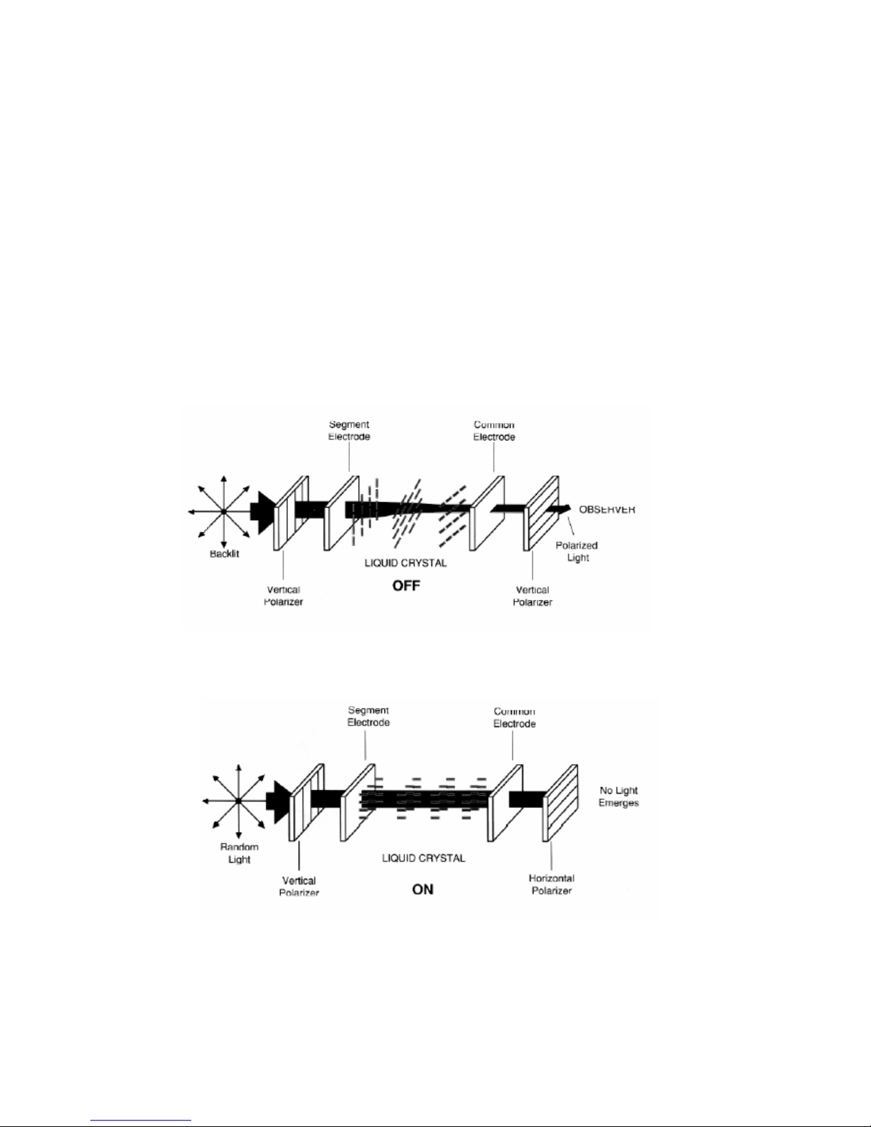
/&'EDVLFGLVSOD\WKHRU\
When an electrical field is applied to the LC planes, the LC molecules re-align
themselves so that they are parallel to the electrical field. This electrical process
is known as twisted nematic field effect or TNFE. In this alignment, polarized
light is not twisted as it passes through the LC material (see Diagram 3A and
3B). If the front polarizer is oriented perpendicular to the rear polarizer, light will
pass through the energized display but will be blocked by the rear polarizer. An
LCD in this form is acting as a light shutter.
Displays with variable characters are created by selectively etching away the
conductive surface that was originally deposited on the glass. Etched areas
become the display’s background; unetched areas become the display’s
characters.
'LDJUDP$
7KHĀRIIāVWDWHRID71/&'WKH/&PROHFXOHVIRUPDWZLVWDQGWKHUHIRUH
FDXVHSRODUL]HGOLJKWWRWZLVWDVLWSDVVHVWKURXJK
'LDJUDP%
7KHĀRQāVWDWHWKHHOHFWULFDOILHOGUHDOLJQVWKH/&PROHFXOHVVRWKH\GR
QRWWZLVWWKHSRODUL]HGOLJKW
36
 Loading...