

Konka Group DLC-3211UT, DLC-3711UT, DLC-2611UT Service Manual

LCD TV SERVICE MANUAL
Model list
DLC-3211UT
DLC-3711UT
DLC-2611UT
KONKA GROUP CO,LTD.
Digital Flat Display Division

IMPORTANT SERVICE SAFETY INFORMATION
Operating the receiver outside of its cabinet or with its back removed involves a shock hazard.
Those who are thoroughly familiar with precautions necessary when working on high voltage
equipment should only perform work on these models.
Exercise care when servicing this chassis with power applied. if carelessly contacted, can cause
serious shock or result in damage to the chassis. Maintain interconnecting ground lead connections
between chassis, escutcheon, picture tube dag and tuner when operating chassis.
When it is necessary to make measurements or tests with AC power applied to the receiver
chassis, an Isolation Transformer must be used as a safety precaution and to prevent possible damage
to transistors. The Isolation Transformer should be connected between the TV line cord plug and the
AC power outlet.
It is important to maintain specified values of all components and anywhere else in the received
that could cause a rise in operating supply voltages. No changes should be made to the original design
of the receiver.
Components shown in the shaded areas on the schematic diagram and/or identified by in the
replacement parts list should be replaced only with exact factory recom mended replacement parts. The
use of unauthorized substitute parts man creates may create shock, fire, or other hazards.
Before returning the receiver to the user, perform the following safety checks:
1. Inspect all lead dress to make certain that leads are not pinched or that hardware is not lodged
between the chassis and other metal parts in the receiver.
2. Replace all protective devices such as non-metallic control knobs, insulating fish papers, cabinet
backs, adjustment and compartment covers of shields, isolation resistor-capacitor networks,
mechanical insulators etc.
3. To be sure that not shock hazard exists, a check for the presence of leakage current should be made
at each exposed metal part having a return path to the chassis (antenna, cabinet metal, screw heads
knobs and/or shafts, escutcheon, etc.) in the following manner.
Plug the AC line cord directly into a 100~240V, AC receptacle. (Do not use an Isolation
Transformer during these checks.) All checks must be repeated with the AC line cord plug connection
reversed. (If necessary, a non-polarized adapter plug must be used only for the purpose of completing
these checks.)
PLEASE READ BEFORE ATTEMPTING SERVICE
1. Use an Isolation Transformer when performing any service on this chassis.
2. Never disconnect any leads while receiver is in operation.
3. Disconnect all power before attempting any repairs.
4. Do not short any position of the circuit while the power is on.
5. For safety reasons, replace components any with identical replacement parts (SEE PARTS LIST).
6. Before alignment, warm up the TV for at least 30 minutes.
7. When removing a PCB or related component, after unfastening or changing a wire, be sure to put
the wire back in its original position.
8. Inferior silicon grease can damage IC's and transistors. When replacing IC's and transis tors, use
only specified silicon grease. Remove all old silicon when applying new silicon.
A. SPECIFICATION
Color System : NTSC_M、ATSC/Free QAM
Sound System : BTSC/SAP
Frequency range: Antenna(2~69)、Cable(2~135)
Audio output power 10%THD 10W X 2
Antenna Impedance 75Ω(Unbalance)
Power Consumption 160W(26”) , 180W(32”),200W(37”)
Power Supply : AC~110-240V, 60Hz
item
Port list
1
RF ANTENNA & Cable
3
Composite
4
S_VIDEO
5
Y、Cb/Pb、Cr/Pr
6
VGA
7
HDMI
8
SPDIF(OUT)
9
AC Input

ADJUSTMENT MANUAL
Ⅰ. TEST NOTE
1
. Please follow the pointed test steps and choose the right test equipment to
conduct adjustment, otherwise good effect of Unit could not be obtained. The
unit should be warmed up for 30 minutes before adjustment and every
parameter should be adjusted repeatedly till the optimum value obtained, the
pointed voltage value should be ensured during test to get satisfied test result.
2. Test environment
1) Temperature
:
15°C-35°C
2) Relative Humidity: 45-75%
3) Air pressure: 86-106Kpa
3 Test equipments(The following equipment should be calibrated before testing
)
1) Computer 1 set
2) Multi-meter (VICTOR VC9801) 1 set
3) Video Signal Generator (Chroma Model 2227/2327) 1 set
4) Color Analyzer (Chroma Model 7120 ) 1 set
5) TV Video Signal Generator (FLUKE PM54200) 1 set
6) ATSC signal Generator (SFU) 1 set
4 Factory mode adjustment
4.1 Enter factory mode adjustment
Using the remote control, press INPUT button once first , then press “2580”
digital keys , and you can see manufacture menu on the LCD panel.
4.2 factory menu operation method
Press the “ . ” key to select the page. Press the “
▽△
” to select the item you
desired change, and press the “< >” to set the value.
4.3 exit the factory menu
Press “Exit” to exit the factory menu , the value you have changed will be
save automatically.
4.4 White calibration adjustment
1 Receive black or white signal under TV、AV or HDMI mode, adjusting
brightness and contrast to set the brightness to 15 Nit in dark area and 90 Nit in
bright area.
2 Adjust white balance. Press“ . ”button to select the page adjusting White
calibration , Press the “
▽△
” to select the item you desired change, and press the
“< >” to set the values as follow.
Red Offset 1000
Green Offset 1000
Blue Offset 1000
3 Then adjusting “Red gain、Green gain、Blue gain” to adjust the chromaticity
coordinates of black and white to fit the requirement.
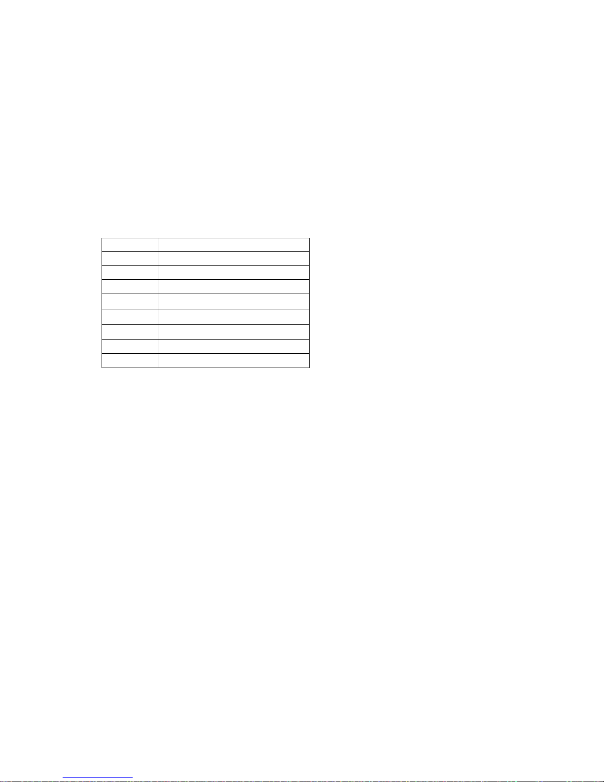
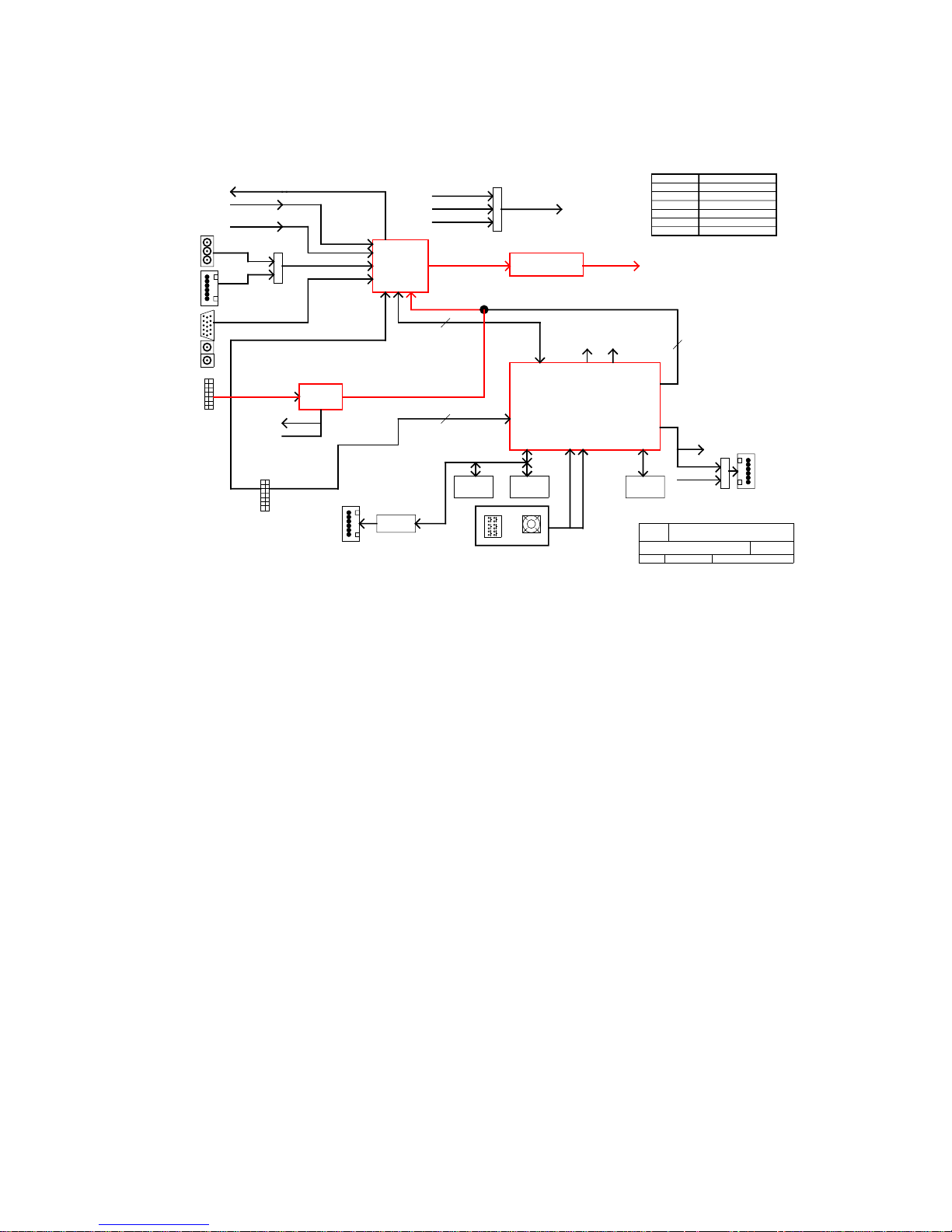
BLOCK DIAGRAM
NC11+3.3V12GND13+2.5V14+1.2V
15
D520D421D322D223D124D0
25
M1
2
9
M2
3
0
M3
31
M4
3
2
NC1NC2+5V3NC4NC5GND6RESET7ERR8NC9NC
10
PSYNC16DE17D718D6
19
CLK26SDA27SCL
28
TDHU1-054A2
TDHU
+B1NC
3
SW.B2NC4Co.15Co.26OOB7GND8GND
9
GND
10
GND
11
GND
12
ALPS_RF-SW
RF
连接线
分配器
AIR
CABLE
TS[0..7]
CVBS
RF_SELECT1
RF_SELECT2
模拟
TV(CVBS) TS流 TO HIDTV
切换开关
I2C
IR
PCI/FLASH/68K
TS1
CAPD/IDE
AnalogRGB
DOUT
MI
I2S/SPDIF
GPIO
ADC
HDA005A Board Block Diagram
24-bit
TS2
06h
8051_BUS
68000 bus
512Kx8
Flash
Y/Pr/Pb2
HiDTV - LX
(8Mx16, 4 pcs)
DDR
I2S
Title
Size
Schematict Name Rev
Date:Sheet
of
Block Diagram 7
KONKA HIDTV ATSC MAIN
B
224
Tuesday, March 21, 2006
CVBS_OUTPUT
THC63LVD103
LVDS OUTPUT
HDMI_SPDIF
I2S
Sil9011
SPDIF
PC
AUDIO
1394/656
8051
(HDCP)
HDMI
TS1 bus
Analog TV1
SWITCH
PC AUDIO
PC_HDTV AUDIO
YPBPR2 AUDIO
YPBPR1 AUDIO
FROM TUNER BOARD
PC IN
Y/Pr/Pb1
SWITCH
SWITCH
SPDIF
HDMI_SPDIF
SVP-EX62
60h/68h
DEVICE
4Eh/4FhPCA9555
SVP-EX62
HiDTV - LX
I2C SLAVE ADDRESS
TVP5147
7Ch/7Dh
Sil9011
S_Video
TEA6415
CVBS
Buttons
Infrared
KEYPAD
(16MB)
FLASH
Ethernet
RJ45
Signal flow chart
Analog TV signal flow chart:
I2C
IR
PCI/FLASH/68K
TS1
CAPD /IDE
AnalogRGB
DOUT
MI
I2S/SPDIF
GPIO
ADC
HDA005A Board Block Diagram
2
4
-
b
i
t
TS2
06h
8051_BUS
68000 bus
512Kx8
Flash
Y/Pr/ Pb2
HiDTV - LX
(8Mx16, 4 pcs )
DDR
I2S
Title
Size
Schematict N ame Rev
Date:Sheet
of
Block Diagram 00
KONKA HIDT V AT S C MAIN
B
224
Thursday, March 23, 2006
CVBS_OUTPUT
THC63LVD103
LVDS OUTPUT
HDMI_SPDIF
I2S
Sil9011
S
P
D
I
F
PC
AUDIO
1394/656
8051
(HDCP)
HDMI
TS1 bus
A
n
a
l
o
g
T
V
1
S
W
I
T
C
H
PC AUDIO
PC_HDTV AUDIO
YPBPR2 AUDIO
YPBPR1 AUDIO
FROM TUNER BOARD
PC IN
Y/Pr/ Pb1
S
W
I
T
C
H
S
W
I
T
C
H
SPDIF
HDMI_SPDIF
SVP-EX62
60h/68h
DEVICE
4Eh/4FhPCA9555
SVP-EX62
HiDT V - L X
I2C SLAVE ADDRESS
TVP5147
7Ch/7Dh
Sil9011
S_Vide o
TEA6415
CVBS
Buttons
Infrared
KEYPAD
(16MB)
FLASH
Ethernet
R
J
4
5
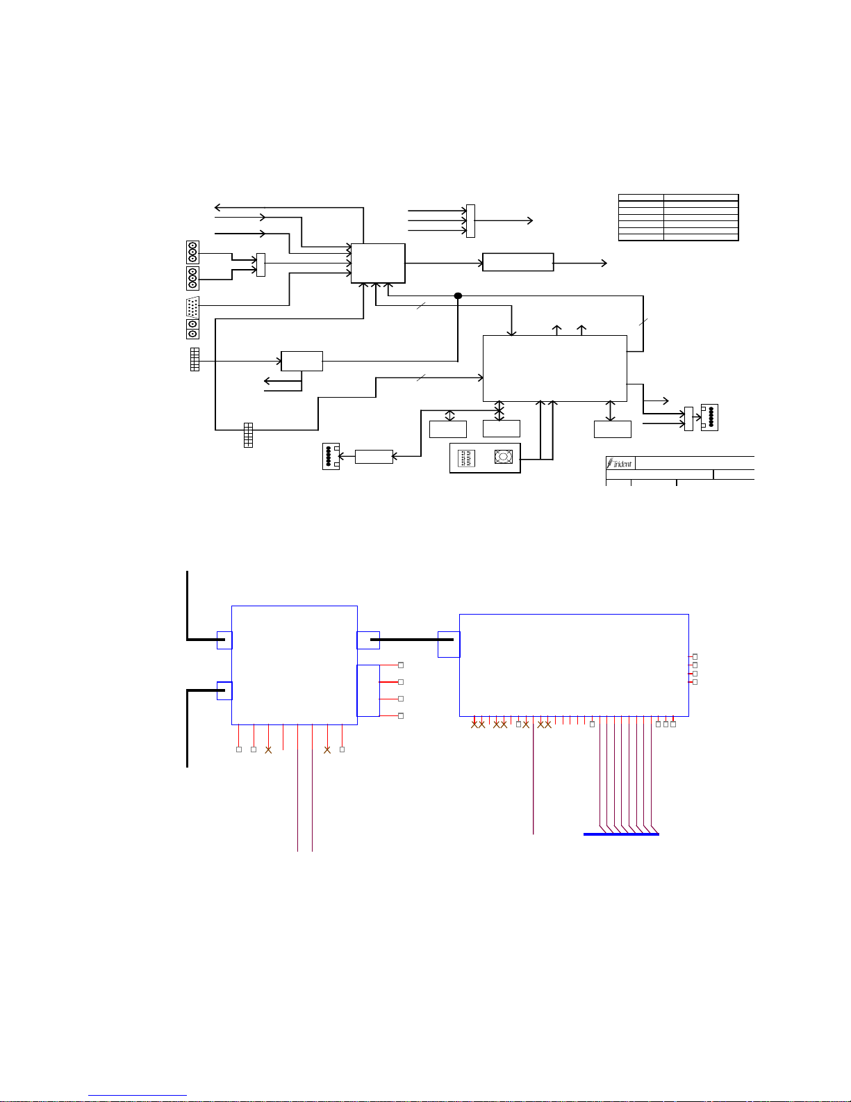
Other analog signal flow chart:
I2C
IR
PCI/FLASH/68K
TS1
CAPD /IDE
AnalogRGB
DOUT
MI
I2S/SPDIF
GPIO
ADC
HDA005A Board Block Diagram
2
4
-
b
i
t
TS2
06h
8051_BUS
68000 bus
512Kx8
Flash
Y/Pr/ Pb2
HiDTV - LX
(8Mx16, 4 pcs )
DDR
I2S
Title
Size
Schematict N ame Rev
Date:Sheet
of
Block Diagram 00
KONKA HIDTV AT S C MAIN
B
224
Thursday, March 23, 2006
CVBS_OUTPUT
THC63LVD103
LVDS OUTPUT
HDMI_SPDIF
I2S
Sil9011
S
P
D
I
F
PC
AUDIO
1394/656
8051
(HDCP)
HDMI
TS1 bus
A
n
a
l
o
g
T
V
1
S
W
I
T
C
H
PC AUDIO
PC_HDTV AUDIO
YPBPR2 AUDIO
YPBPR1 AUDIO
FROM TUNER BOARD
PC IN
Y/Pr/ Pb1
S
W
I
T
C
H
S
W
I
T
C
H
SPDIF
HDMI_SPDIF
SVP-EX62
60h/68h
DEVICE
4Eh/4FhPCA9555
SVP-EX62
HiDT V - L X
I2C SLAVE ADDRESS
TVP5147
7Ch/7Dh
Sil9011
S_Video
TEA6415
CVBS
Buttons
Infrared
KEYPAD
(16MB)
FLASH
Ethernet
R
J
4
5
Digital TV signal flow chart:
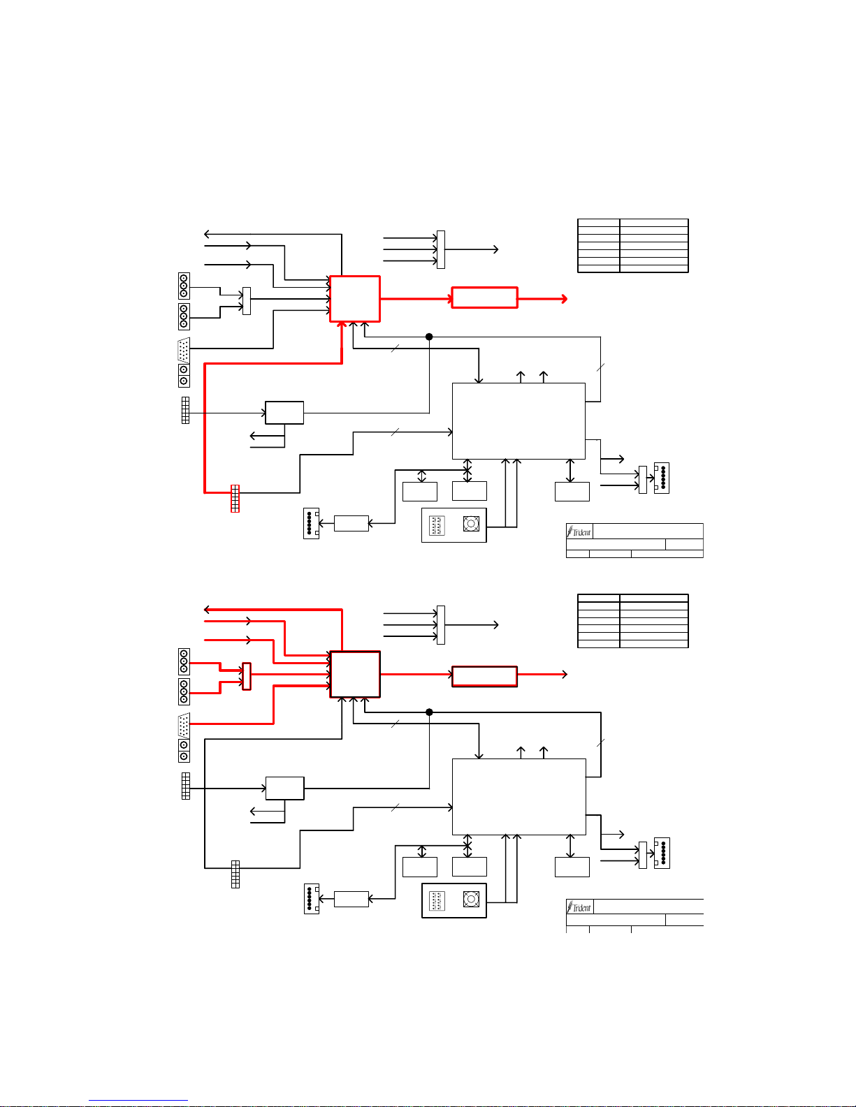
HDMI signal flow chart:
HiDTV - LX
CAPD/IDE
8051
YPBPR2 AUDIO
CVBS
RJ45
FLASH
SPDIF
1394/656
YPBPR1 AUDIO
TS1 bus
S_Video
I2C SLAVE ADDRESS
SWITCH
KEYPAD
PC AUDIO
(HDCP)
Analog TV1
SPDIF
Block Diagram 5
KONKA HIDTV ATSC MAIN
B
224
Monday, December 05, 2005
Title
Size
Schematict Name Rev
Date:Sheet
of
TVP5147
HDMI
CVBS_OUTPUT
FROM TUNER BOARD
PC IN
(16MB)
IR
512Kx8
Flash
Y/Pr/Pb1
THC63LVD103
SVP-EX62
PCI/FLASH/68K
68000 bus
DEVICE
06h
(8Mx16, 4 pcs)
4Eh/4Fh
TS2
TEA6415
I2S
LVDS OUTPUT
I2S/SPDIF
Infrared
Sil9011
TS1
24-bit
Sil9011
AnalogRGB
PCA9555
PC
AUDIO
HDA005A Board Block Diagram
DOUT
PC_HDTV AUDIO
SWITCH
ADC
HDMI_SPDIF
8051_BUS
I2C
I2S
GPIO
60h/68h
SVP-EX62
Buttons
MI
7Ch/7Dh
HDMI_SPDIF
HiDTV - LX
Y/Pr/Pb2
Ethernet
SWITCH
DDR
IC BLOCK DIAGRAM
1 U15
(HiDTV)
TS1 bus
LVDS OUTPUT
SWITCH
06h
I2S/SPDIF
Block Diagram 5
KONKA HIDTV ATSC MAIN
B
224
Monday, December 05, 2005
Title
Size
Schematict Name Rev
Date:Sheet
of
I2C SLAVE ADDRESS
SPDIF
Ethernet
THC63LVD103
AnalogRGB
TVP5147
FROM TUNER BOARD
CVBS_OUTPUT
8051
FLASH
Y/Pr/Pb1
SWITCH
(8Mx16, 4 pcs)
SVP-EX62
1394/656
KEYPAD
DDR
SVP-EX62
DEVICE
CAPD/IDE
TS2
(HDCP)
(16MB)
I2C
4Eh/4Fh
RJ45
I2S
I2S
TEA6415
24-bit
HDMI
HiDTV - LX
Sil9011
HDA005A Board Block Diagram
8051_BUS
Y/Pr/Pb2
Sil9011
PC_HDTV AUDIO
ADC
PCA9555
HDMI_SPDIF
SWITCH
YPBPR2 AUDIO
CVBS
YPBPR1 AUDIO
Infrared
DOUT
HDMI_SPDIF
60h/68h
Analog TV1
PC AUDIO
7Ch/7Dh
MI
PC IN
IR
S_Video
PC
AUDIO
512Kx8
Flash
HiDTV - LX
TS1
PCI/FLASH/68K
GPIO
SPDIF
Buttons
68000 bus
 Loading...