

Page 1

SERVICE MANUAL
Color Television Receiver
Model: TK-A/Q Series
Page 2

SERVICE MANUAL TK-A/Q
CONTENTS
I. IMPORTANT SERVICE SAFETY INFORMATION…………………… 3
II. ALIGNMENT PROCEDURES PLEASE READ BEFORE
ATTEMPTING SERVICE…………………………………………………… 5
III. TV SPECIFICATION……………………………………………………. 6
IV. TV ADJUSTMENT……………………………………………………….. 9
V. IC INFORMATION……………………………………………………….. 13
1. PHILIPS UOCIII CHIP (N603)……………………………………………………….. 13
2. EEPROM 24C16 (N602)……………………………………………………………….. 53
3. SWITCH POWER IC (N901)…………………………………………………………. 57
4. VERTICAL DEFLECTION BOOSTER (N401)…………………………………….. 61
5. AUDIO POWER AMPLIFIER (N202)……………………………………………….. 66
VI. TV BLOCK DIAGRAM………………………………………………….. 74
IMPORTANT SERVICE SAFETY INFORMATION
Operating the receiver outside of its cabinet or with its back removed involves a shock hazard.
Work on these models should only be performed by those who are thoroughly familiar with
2
Page 3

SERVICE MANUAL TK-A/Q
precautions necessary when working on high voltage equipment.
Exercise care when servicing this chassis with power applied. Many B plus and high voltage
RF terminals are exposed which, if carelessly contacted, can cause serious shock or result in damage
to the chassis. Maintain interconnecting ground lead connections between chassis, escutcheon,
picture tube dag and tuner when operating chassis.
These receivers have a “polarized” AC line cord. The AC plug is designed to fit into standard
AC outlets in one direction only. The wide blade connects to the “ground side” and the narrow blade
connects to the hot “side” of the AC line. This assures that the TV receiver is properly grounded to
the house wiring. If an extension cord must be used, make sure it is of the “polarized” type.
Since the chassis of this receive is connected to one side of the AC supply during operation,
service should not be attempted by anyone not familiar with the precautions necessary when
working on these types of equipment.
When it is necessary to make measurements or tests with AC power applied to the receiver
chassis, an Isolation Transformer must be used as a safety precaution and to prevent possible
damage to transistors. The Isolation Transformer should be connected between the TV line cord
plug and the AC power outlet.
Certain High voltage (HV) maybe cause X-ray radiation. Receivers should not be operated with
HV levels exceeding the specified rating for their chassis type. Higher voltage may also increase the
possibility of failure in the HV supply.
It is important to maintain specified values of all components in the horizontal and high voltage
circuits and anywhere else in the receive that could cause a rise in high voltage, or operating supply
voltages. No changes should be made the original design of the receiver.
Components shown in the shaded areas on the schematic diagram and/or identified by in the
replacement parts list should be replaced only with exact factory recommended replacement parts.
The use of unauthorized substitute parts man creates may create shock, fire, X-ray radiation, or other
hazards.
To determine the presence of high voltage, use an accurate high impedance HV meter
connected between the second anode lead and he CRT dag grounding device. When servicing the
High Voltage System remove static charges from it by connecting a 10K Ohm resistor in series Wan
insulated wire(such as test probe) between the picture tube dag and 2nd anode lead(Have AC line
cord disconnected from AC supply).
3
Page 4

SERVICE MANUAL TK-A/Q
The picture tube use in this receiver employ integral implosion protection. Replace with a tube
of the same type number for continued safety. Do not lift picture tube by the neck. Handle the
picture tube only when wearing shatterproof goggles and after discharging the high voltage
completely, Keep others without shatter proof goggles away.
Before returning the receiver to the user, perform the following safety checks:
1. Inspect all lead dress to make certain that leads are not pinched or that hardware is not
lodged between the chassis and other metal parts in the receiver.
2. Replace all protective devices such as non-metallic control knobs, insulating fish-papers,
cabinet backs, adjustment and compartment covers of shields, isolation resistor-capacitor networks,
mechanical insulators etc.
3. To be sure that not shock hazard exists, a check for the presence of leakage current should be
made at each exposed metal part having a return path to the chassis (antenna, cabinet metal, screw
heads knobs and/or shafts, escutcheon, etc.) in the following manner.
Plug the AC line cord directly into a 110V/220V/240V AC receptacle. (Do not use an Isolation
Transformer during these checks.) All checks must be repeated with the AC line cord plug
connection reversed. (If necessary, a non-polarized adapter plug must be used only for the purpose
of completing these checks.)
If available, measure the current using an accurate leakage current tester. Any reading of
0.35mA or more is excessive and indicates a potential shock hazard which must be corrected before
returning the receiver to owner.
If a reliable leakage current tester is not available, this alternate method of measurement should
be used. Using two clip leads, connect a 1500 Ohm, 10 watt resistor paralleled by a 0.15MF
capacitor in series with a known earth ground, such as a water pipe or conduit and the metal part to
be checked. Use a VTVM or VOM with 1000 Ohms per Volt, or higher, sensitivity to measure this
AC voltage drop across the resistor,. Any reading of 0.35 volt RMS of more is excessive and
indicates potential shock hazard which must be corrected before returning he receiver to the owner.
ALIGNMENT PROCEDURES
PLEASE READ BEFORE ATTEMPTING SERVICE
1. Use an Isolation Transformer when performing any service on this chassis.
4
Page 5

SERVICE MANUAL TK-A/Q
2. Never disconnect any leads while receiver is in operation.
3. Disconnect all power before attempting an repairs.
4. Do not short any position of the circuit while the power is on.
5. For safety reasons, replacing any components should be according with identical replacement
parts.
6. Before testing, warm up the TV for at least 30 minutes and demagnetize the CRT with an external
degaussing coil.
7. When removing a PCB or related component, after unfastening or changing a wire, be sure to put
the wire back in its original position.
8. Inferior silicon grease can damage IC’s and transistors. When replacing IC’s and transistors, use
only specified silicon grease,. Remove all old silicon when applying new silicon.
9. Before removing the anode cap, discharge drastically because it contains high voltage.
TV SPECIFICATION
1. Ambient Conditions:
1.1 Ambient Temperatures:
5
Page 6

SERVICE MANUAL TK-A/Q
a. Operating: -10 ~ +40 ℃
b. Storage: -15 ~ +45 ℃
1.2 Humidity
a. Operation: <80%
b. Storage: <90%
1.3 Air Pressure: 86kpa ~ 106kpa
2. General Specification
2.1 Main IC: Philips UOCIII chip
2.2 System: TV PAL DK/BG/I
SECAM DK/BG/L(L’)
NTSC M
AV PAL
SECAM
NTSC 4.43/3.58
2.3 Channel: VHF-LOW 46.25~140.25MHz
VHF-HIGH 147.25~423.25MHz
UHF 431.25~855.25MHz
CATV 112.25~464.25MHz
2.4 Scanning Lines & Frequencies
525 lines/60Hz or 625 lines/50Hz
15.75KHz/15.625KHz
2.5 Color Sub-Carrier Frequency: 4.433MHz/3.579MHz
2.6 IF: Picture 38.9MHz/38.0MHz/45.75MHz
Sound 4.5MHz/5.5MHz/6.0MHz/6.5MHz
2.7 Power Consumption: 14” and 15” TV 70W
21” TV 75W
29” TV 150W
6
Page 7

SERVICE MANUAL TK-A/Q
34” TV 180W
2.7 Power Supply:
AC 110/220/240V 50/60 Hz
2.8 Max Audio Output Power (7% THD): 14” and 15” ≥1W X 2
21” ≥1.5W X 2
29” and 34” ≥4W X 2
2.9 Antenna Impedance: 75Ω
3. Basic Features of Controller
3.1 Channel Tuning Method: Frequency Synthesizer
3.2 Preset table Program: 240 Programs or 100 Programs
3.3 Tuning for VHF and UHF Bands: Auto Tuning/Manual Tuning
3.4 Picture and Sound Adjustment:
Bright, Contrast, Color, Sharpness control and Color Temperature adjustment
TINT control (NTSC only)
Volume, Balance, Bass, Treble control
3.5 OSD:
General Features (Volume, Balance, Bass, Treble, Brightness, Contrast, Color, Sharpness,
Program, Auto Search, Manual Tune, Muting, AV/TV, Child Lock and Sleep Timer)
Multi-Language (including English)
3.6 Sleep Timer: 5 -120 Minutes with 5 Minutes Increment
3.7 Auto Standby When No Signal in 5 minutes
3.8 Full Function Infrared Remote Control
8m
3.9 Remote Effective Distance:
4. Construction of Front Panel
Main Power Switch
Remote Sensor
Standby Indicator
Menu Select Button
TV/AV Select Button
Program and Volume Up/Down Button
7
Page 8

SERVICE MANUAL TK-A/Q
5. TV’s Terminals
75 Ω Aerial Terminal
AV Input and AV Output (TK-A Series)
S-Video Input
Y/U/V Input
SCART Input and Output (TK-Q Series)
6. Other Informations
6.1 Magnetic Field:
Bv = 0.3~0.65Gs
6.2 Standard Color Temperature: 9300K (X = 0.284, Y = 0.299)
TV ADJUSTMENT
Test equipment
8
Page 9

SERVICE MANUAL TK-A/Q
1. Oscilloscope
2. Multifunction meter (Internal resistance: DC≥20kΩ/V AC≥5kΩ/V)
3. High voltmeter: 35kV
4. Standard Signal Generator
5. Degaussing coil
Factory menu
Some adjustments must be performed in the Factory menu. You can enter the Factory menu in
the following way:
1. Press the MENU button on the remote control then press the Q.VIEW button on the remote
control at least 5 times immediately.
2. Press the MENU buttons to select the desired Factory menu pages or press 0-9 number buttons to
enter the Factory menu pages directly and then press the PROG.+/- buttons to select the desired
items.
3. Press the VOL+/- buttons to change the settings.
B+ adjustment
Test Equipment: Multifunction meter
1. Operate the TV set with AC 110/220/240V(50/60Hz).
2. Receive Television broadcast signal, set PICTURE to Normal mode.
2. Connect the multifunction meter + lead to C960 and GND. Adjust the RP950 until the meter
reading the proper DC value (More details please refer to the TV’s BOM ).
High voltage check and filament voltage check
Test Equipment: High voltmeter
1. Make sure AC power supply and +B are within pointed range before calibrating high voltage.
2. Connect high voltmeter to anode (G4) of CRT and GND.
3. Turn on the TV, set the BRIGHTNESS and CONTRAST to the minimum (zero beam current),
swap to AV mode (No any signal applied).
9
Page 10

SERVICE MANUAL TK-A/Q
4. High voltage please refer to different CRT
5. Filament voltage measured by virtual value meter please see the related model BOM, usually
within the range of 6.3±0.2Vrms.
Grid voltage adjustment
1. Enter into Factory menu, set VG2, VSD, then adjust potentiometer to IN/OUT flash on the screen.
VG2 XX Please see the related model’s BOM
VSD Brightness XX Please see the related model’s BOM
VSD XX Please see the related model’s BOM
2. Receive PHILIPS five circles pattern after settings finishing, set PICTURE to Normal mode.
RF AGC adjustment
1. Receive a 60dBμV gray scale signal(PAL or SECAM).
2. Enter Factory menu and select AGC TAKE OVER, then adjust it until the picture noise is just
disappeared.
Focus adjustment
1. Receive five circles pattern, adjust the pattern to Normal mode.
2. Adjust focus potentiometer (horizontal output transformer) so that the center and four corners of
pattern are the best focus.
Horizontal scanning, vertical scanning and geometry correction adjustment
(adjust with PAL and NTSC signal separately)
1. Enter into factory menu to call up FAC1
EW WIDTH 50(60) XX Adjust it so that the picture horizontal reproduction display
ratio is more than 92% (H- size adjustment).
HOR.SHIFT 50(60) XX Adjust it so that the left half is symmetrical with the right
half (H. CEN correction).
10
Page 11

SERVICE MANUAL TK-A/Q
EW PARABOLA 50(60) XX Adjust it so that parallelogram will be transformed to
rectangle or trapezium (Receive cross hatch signal)(Parallelogram correction).
TRAPEZIUM
(Receive cross hatch signal)(Trapezium).
UC PARABOLA 50(60) XX Adjust it so that upper corner (left and right) vertical line are
straight line (Receive cross hatch signal)(Upper corner pincushion).
LC PARABOLA 50(60) XX Adjust it so that bottom corner (left and right) vertical line
are straight line (Receive cross hatch signal)(Bottom correction pincushion).
HOR.BOW 50(60) XX Adjust it so that vertical line is the straight line.(Receive
cross hatch signal) (Bow correction).
PARALLEL 50(60) XX Adjust it so that left and right line are straight lines
(Pincushion correction).
2. Receive five circles pattern signal, enter into factory menu to call up FAC2.
VERT SLOPE 50(60) XX Adjust it so that horizontal midline of the pattern superpose
with the black edge of the pattern.
50(60) XX Adjust it so that trapezium distortion is just disappeared
VERT SHIFT 50(60) XX Adjust it so that the pattern midline superposes over CRT
geometric center.
VERT AMPLE 50(60) XX Adjust it so that the picture vertical reproduction display ratio
is more than 92%.
S CORR 50(60) XX Adjust it so that upper pane and bottom pan of the pattern are
the same as the middle pane.
V.LIN.CTRL 50(60) 0
V.LINEARITY 50(60) XX Adjust vertical linear.
VERT ZOOM 50(60) 25 Adjust vertical amplitude(fixed value 25).
White balance adjustment (PAL or SECAM signal)
1. Enter into menu firstly and set PICTURE to Normal mode. (9300K)
11
Page 12
SERVICE MANUAL TK-A/Q
2. Enter into AV mode and receive left black right white signal which with color sync signal.
3. Plug XS805, adjust it automatically with white balance adjustment software, enter into factory
menu when adjustment is OK, then enter into FAC 6、FAC 7、FAC 8 menu to check the following
data are consistent with data in computer.
Standard: Color temperature 9300K (X=0.284 Y=0.299) FAC 6
Warm color: Color temperature 6500K (X=0.313 Y=0.329) FAC 7
Cold color: Color temperature 12000K(X=0.272 Y=0.279) FAC 8
FAC 6
ADJ content
X=0.284
Y=0.299
BLOR-N xx BLOR-W xx BLOR-C xx
BLOG-N xx BLOG-W xx BLOG-C xx
WPR-N xx WPR-W xx WPR-C xx
WPR-N xx WPG-W xx WPG-C xx
WPR-N xx WPB-W xx WPB-C xx
value
FAC 7
ADJ Content
X=0.313
Y=0.329
value
FAC 8
ADJ Content
X=0.272
Y=0.279
value
Other factory menu data
Each TV model has different factory menu, more details please refer to the TV’s adjustment
Engineering Illumination.
IC INFORMATION
1. PHILIPS UOCIII CHIP – TDA110XXH1/TDA120XXH1 (N603)
12
Page 13

SERVICE MANUAL TK-A/Q
1.1 General description
The UOCIII series combines the functions of a Video Signal Processor (VSP) together with a
FLASH embedded TEXT/Control/Graphics µ-Controller (TCG µ-Controller) and US Closed
Caption decoder. In addition the following functions can be added:
Adaptive digital (4H/2H) PAL/NTSC comb filter
•
• Teletext decoder with 10 or 100 page text memory
Multi-standard stereo decoder
•
• BTSC stereo decoder
Digital sound processing circuit
•
• Digital video processing circuit
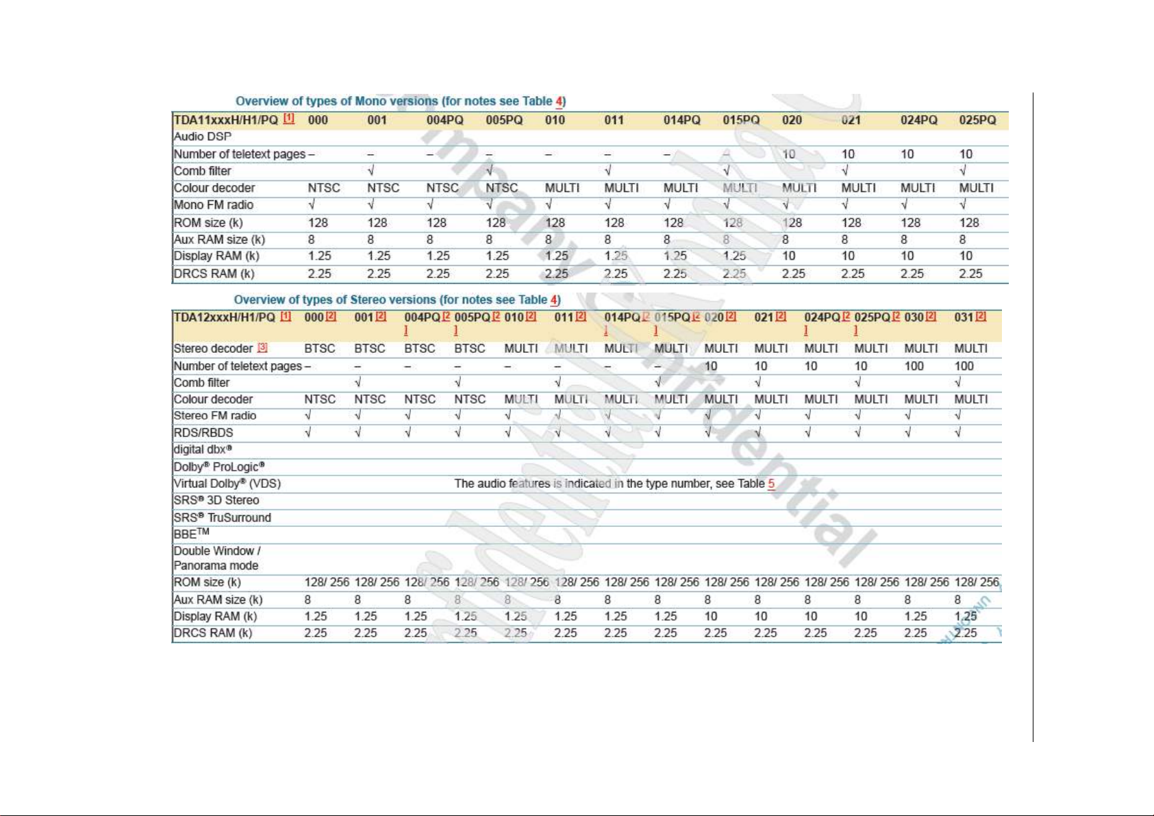
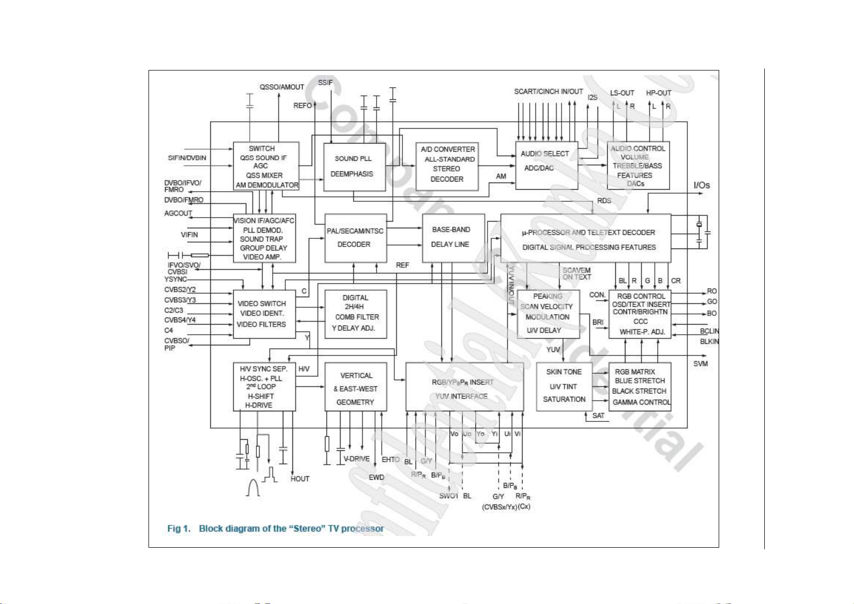
The UOCIII series consists of the following 3 basic concepts:
• Stereo versions. These versions contain the TV processor with a stereo audio selector, the TCG
µ-Controller, the multi-standard stereo or BTSC decoder, the digital sound processing circuit and
the digital video processing circuit. Options are the adaptive digital PAL/NTSC comb filter and a
teletext decoder with 10 or 100 page text memory.
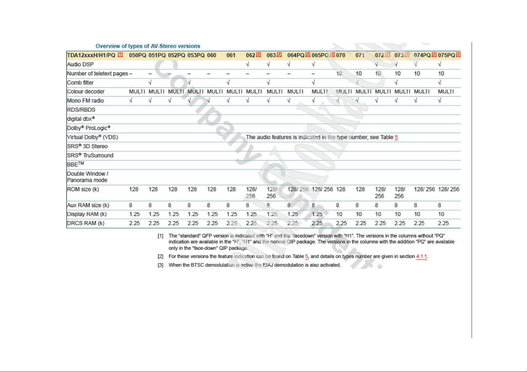
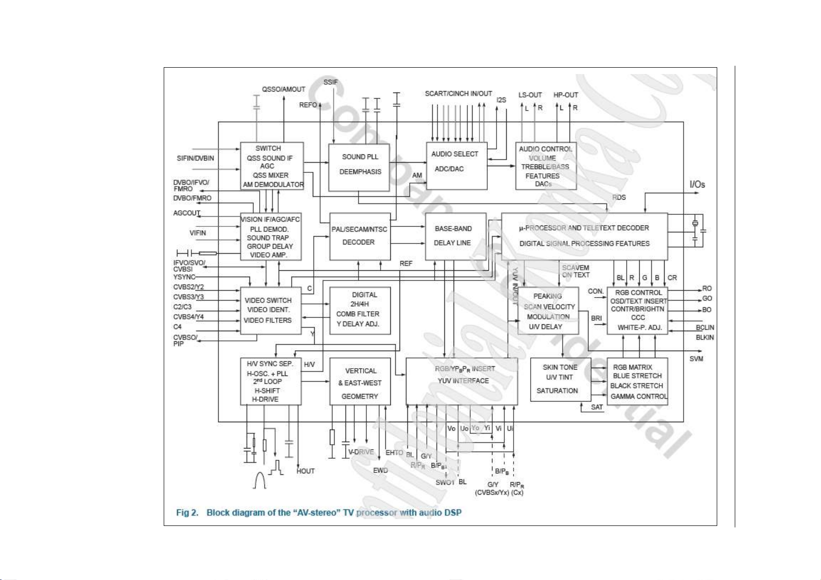
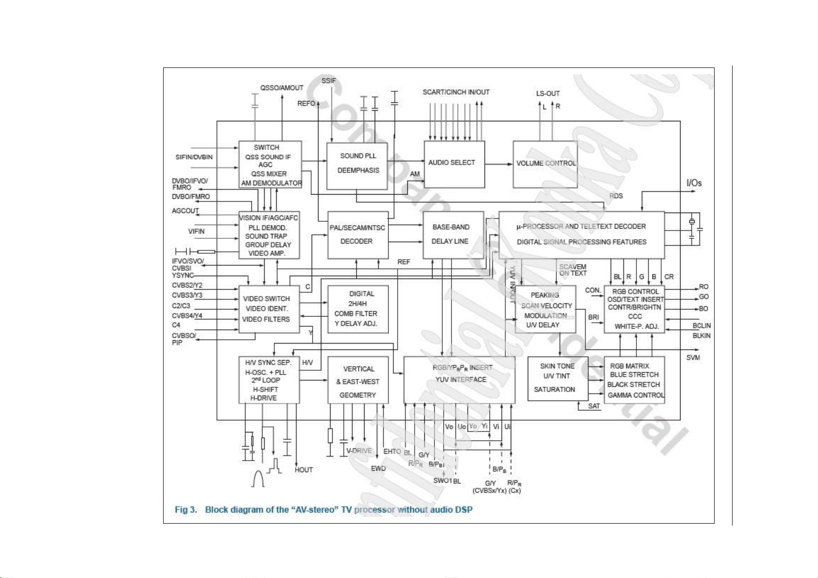
• AV stereo versions. These versions contain the TV processor with stereo audio selector and the
TCG µ-Controller. Options are the digital sound processing circuit, the digital video processing
circuit, the adaptive digital PAL/NTSC comb filter and a teletext decoder with a 10 page text
memory.
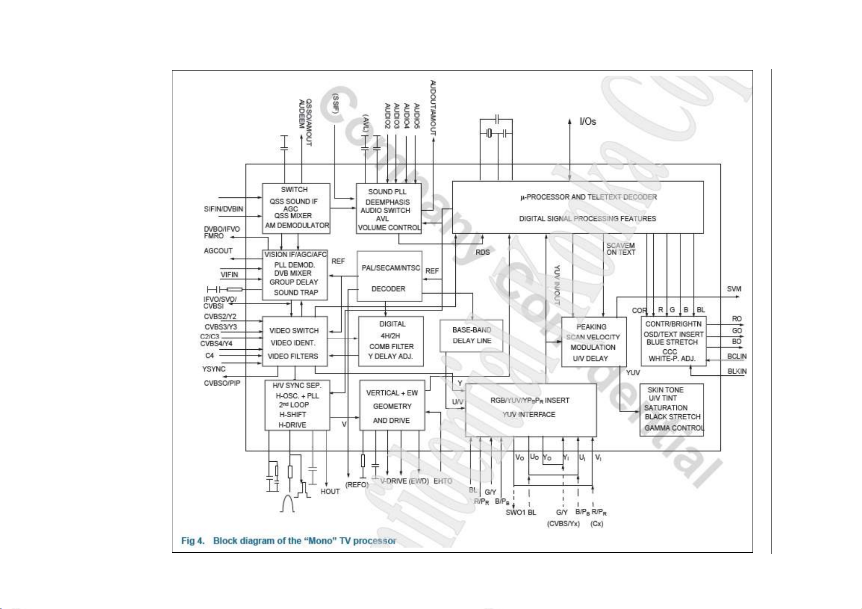
• Mono sound versions. These versions contain the TV processor with a selector for mono audio
signals and the TCG µ-Controller. Options are the adaptive digital PAL/NTSC combfilter and a
teletext decoder with 10 page text memory.
The ICs are mounted in a QFP-128 package and can be used in economy television receivers
with 90 and 110 picture tubes. The package is according to the ROHS legislation, which also
means that the package is lead-free. The ICs have supply voltages of 5V, 3.3V. Also an 1.8V supply
is needed, but this can be simply derived by adding an emitter follower at a reference voltage from
the device.
1.2 Features
1.2.1 Analogue Video Processing (all versions)
13
Page 14

SERVICE MANUAL TK-A/Q
* Multi-standard vision IF circuit with alignment-free PLL demodulator
* Internal (switchable) time-constant for the IF-AGC circuit
* Switchable group delay correction and sound trap (with switchable centre frequency) for the
demodulated CVBS signal
* DVB/VSB IF circuit for preprocessing of digital TV signals.
* Video switch with 3 external CVBS inputs and a CVBS output. All CVBS inputs can be used as
Y-input for Y/C signals. However, only 2 Y/C sources can be selected because the circuit has 2
chroma inputs. It is possible to add an additional CVBS(Y)/C input (CVBS/YX and CX) when the
YUV interface and the RGB/YPBPR input are not needed. It is also possible to insert a CVBS/Y
signal at the SVO/IFVOUT output.
* Automatic Y/C signal detector
* Integrated luminance delay line with adjustable delay time
* Picture improvement features with peaking (with switchable centre frequency, depeaking, variable
positive/negative peak ratio, variable pre-/overshoot ratio and video dependent coring), dynamic
skin tone control, gamma control and blue- and black stretching. All features are available for CVBS,
Y/C and RGB/YPBPR signals.
* The effect of the various features can de demonstrated by means of a ‘split screen’ mode in which
the features are activated in one half of the picture and switched off in the other half
* Switchable DC transfer ratio for the luminance signal
* Only one reference (24.576 MHz) crystal required for the TCG µ-Controller, and the colour
decoder
* Multi-standard colour decoder with automatic search system and various “forced mode”
possibilities
* Internal base-band delay line
* Indication of the Signal-to-Noise ratio of the incoming CVBS signal
* Linear RGB/YPBPR input with fast insertion.
* YUV interface. When this feature is not required some pins can be used as additional
RGB/YPBPR input. It is also possible to use these pins for additional CVBS (or Y/C) input
(CVBS/YX and CX).
* Tint control for external RGB/YPBPR signals
* Scan Velocity Modulation output. The SVM circuit is active for all the incoming CVBS, Y/C and
14
Page 15

SERVICE MANUAL TK-A/Q
RGB/YPBPR signals.
* RGB control circuit with ‘Continuous Cathode Calibration’, white point and black level off-set
adjustment so that the colour temperature of the dark and the light parts of the screen can be chosen
independently.
* Contrast reduction possibility during mixed-mode of OSD
* Adjustable ‘wide blanking’ of the RGB outputs
* Horizontal synchronization with two control loops and alignment-free horizontal oscillator
* Vertical count-down circuit
* Vertical driver optimized for DC-coupled vertical output stages
* Horizontal and vertical geometry processing with horizontal parallelogram and bow correction and
horizontal and vertical zoom
* Low-power start-up of the horizontal drive circuit
1.2.2 Analogue Sound Processing
1.2.2.1 Mono versions
* The low-pass filtered ‘mixed down’ I signal is available via a single ended output stage
1.2.2.2 Stereo versions
* The low-pass filtered ‘mixed down’ I signal is available via a single ended or balanced output
stage.
1.2.3 Sound Demodulation (all versions)
* Separate SIF (Sound IF) input for single reference QSS (Quasi Split Sound) demodulation.
* AM demodulator without extra reference circuit
* The mono intercarrier sound circuit has a selective FM-PLL demodulator which can be switched
to the different FM sound frequencies (4.5/5.5/6.0/6.5 MHz). The quality of this system is such that
the external band-pass filters can be omitted.
* The FM-PLL demodulator can be set to centre frequencies of 4.72/5.74 MHz so that a second
sound channel can be demodulated. In such an application it is necessary that an external bandpass
filter is inserted.
* The vision IF and mono intercarrier sound circuit can be used for the demodulation of FM radio
signals. With an external FM tuner also signals with an IF frequency of 10.7 MHz can be
15
Page 16

demodulated.
SERVICE MANUAL TK-A/Q
* Switch to select between 2nd SIF from QSS demodulation or external FM (SSIF).
1.2.4 Audio Interfaces and Switching
1.2.4.1 Mono versions
* Audio switch circuit with 4 external audio (mono) inputs and a volume controlled output
* AVL circuit
1.2.4.2 AV stereo versions without audio DSP
* Audio switch circuit with 4 stereo inputs, a stereo output for SCART/CINCH and a stereo
SPEAKER output with independent L&R analogue volume control.
* Analogue mono AVL circuit at left audio channel
1.2.4.3 Stereo versions with audio DSP
* Audio switch circuit with 4 stereo inputs, a stereo output for SCART/CINCH, 1 stereo output for
HEADPHONE. The headphone channel has an analogue volume control circuit for the L and R
channel. Finally 1 stereo SPEAKER output with digital controls.
* AVL (Automatic Volume Levelling) circuit for the headphone channel.
* Digital input crossbar switch for all digital signal sources and destinations
* Digital output crossbar for exchange of channel processing functionality
* Digital audio input interface (stereo I2S input interface)
* Digital audio output interface (stereo I2S output interface)
1.2.5 Stereo Demodulator and Decoder (full stereo versions)
* Demodulator and Decoder Easy Programming (DDEP)
* Auto standard detection (ASD)
* Static Standard Selection (SSS)
* DQPSK demodulation for different standards, simultaneously with 1-channel FM demodulation
* NICAM decoding (B/G, I, D/K and L standard)
* Two-carrier multistandard FM demodulation (B/G, D/K and M standard)
* Decoding for three analog multi-channel systems (A2, A2+ and A2*) and satellite sound
* Adaptive de-emphasis for satellite FM
16
Page 17

SERVICE MANUAL TK-A/Q
* Optional AM demodulation for system L, simultaneously with NICAM
* Identification A2 systems (B/G, D/K and M standard) with different identification time constants
* FM pilot carrier present detector
* Monitor selection for FM/AM DC values and signals, with peak and quasi peak detection option
* BTSC MPX decoder
* SAP decoder
* digital dbx® noise reduction 3 4
* Japan (EIAJ) decoder
* FM radio decoder
* Soft-mute for DEMDEC outputs DEC, MONO and SAP
* FM overmodulation adaptation option to avoid clipping and distortion
1.2.6 Audio Multi Channel Decoder (versions with audio DSP)
* Dolby® Pro Logic® (DPL) 5 4
* Virtual Dolby® Surround (VDS) 6
* Five channel processing for Main Left and Right, Subwoofer, Centre and Surround. To exploit this
feature an external DAC is required.
1.2.7 Volume and tone control for loudspeakers (versions with Audio DSP)
* Automatic Volume Level (AVL) control
* Smooth volume control
* Master volume control
* Soft-mute
* Loudness
* Bass, Treble
* Five band graphic equalizer
* Dynamic Bass Boost (DBB) 7
* Dynamic Virtual Bass (DVB) 8
* BBE® Sound processing 3 4
* Processed or non processed subwoofer output
* Programmable beeper
17
Page 18

SERVICE MANUAL TK-A/Q
1.2.8 µ-Controller
* 80C51 µ-Controller core standard instruction set and timing
* 0.4883 µs machine cycle
* maximum of 256k x 8-bit flash programmable ROM
* maximum of 8k x 8-bit Auxiliary RAM
* 12-level Interrupt controller for individual enable/disable with two level priority
* Two 16-bit Timer/Counter registers
* One 24-bit Timer (16-bit timer with 8-bit Pre-scaler)
* Watch Dog timer
* Auxiliary RAM page pointer
* 16-bit Data pointer
* Stand-by, Idle and Power Down modes
* 24 general-purpose I/O pins
* 14 bits PWM for Voltage Synthesis Tuning
* 8-bit A/D converter with 4 multiplexed inputs
* 5 PWM (6-bits) outputs for analogue control functions
* I2C byte level bus interface.
* Remote Control Pre-processor (RCP)
* Universal Asynchronous Receiver Transmitter (UART)
1.2.9 Data Capture
* Text memory max up to 100 pages
* Inventory of transmitted Teletext pages stored in the Transmitted Page Table (TPT) and Subtitle
Page Table (SPT)
* Data Capture for US Closed Caption
* Data Capture for 525/625 line WST, VPS (PDC system A) and 625 line Wide Screen Signalling
(WSS) bit decoding
* Automatic selection between 525 WST/625 WST
* Automatic selection between 625 WST/VPS on line 16 of VBI
* Real-time capture and decoding for WST Teletext in Hardware, to enable optimized m-processor
throughput
18
Page 19

SERVICE MANUAL TK-A/Q
* Automatic detection of FASTEXT transmission
* Real-time packet 26 engine in Hardware for processing accented, G2 and G3 characters
* Signal quality detector for video and WST/VPS data types
* Comprehensive teletext language coverage
* Vertical Blanking Interval (VBI) data capture of WST data
1.2.10 Display
* 50Hz/60Hz display timing modes
* Two page operation for 16:9 screens
* Serial and Parallel Display Attributes
* Single/Double/Quadruple Width and Height for characters
* Smoothing capability of both Double Size, Double Width & Double Height characters
* Scrolling of display region
* Variable flash rate controlled by software
* Soft colours using CLUT with 4096 colour palette
* Globally selectable scan lines per row (9/10/13/16/) and character matrix [12x9, 12x13, 12x16,
16x18, (VxH)]
* Fringing (Shadow) selectable from N-S-E-W direction
* Fringe colour selectable
* Contrast reduction of defined area
* Cursor
* Special Graphics Characters with two planes, allowing four colours per character
* 64 software redefinable On-Screen display characters
* 4 WST Character sets (G0/G2) in single device (e.g. Latin, Cyrillic, Greek, Arabic)
* G1 Mosaic graphics, Limited G3 Line drawing characters
* WST Character sets and Closed Caption Character set in single device
* Curtaining effect via software
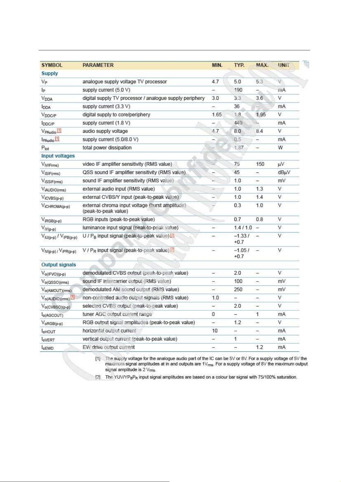
1.3 Quick reference data
19
Page 20
SERVICE MANUAL TK-A/Q
1.4 Ordering Options
20
Page 21
21
SERVICE MANUAL TK-A/Q
Page 22
22
SERVICE MANUAL TK-A/Q
Page 23
23
1.5 Block diagram
SERVICE MANUAL TK-A/Q
Page 24
24
SERVICE MANUAL TK-A/Q
Page 25
25
SERVICE MANUAL TK-A/Q
Page 26
26
SERVICE MANUAL TK-A/Q
Page 27
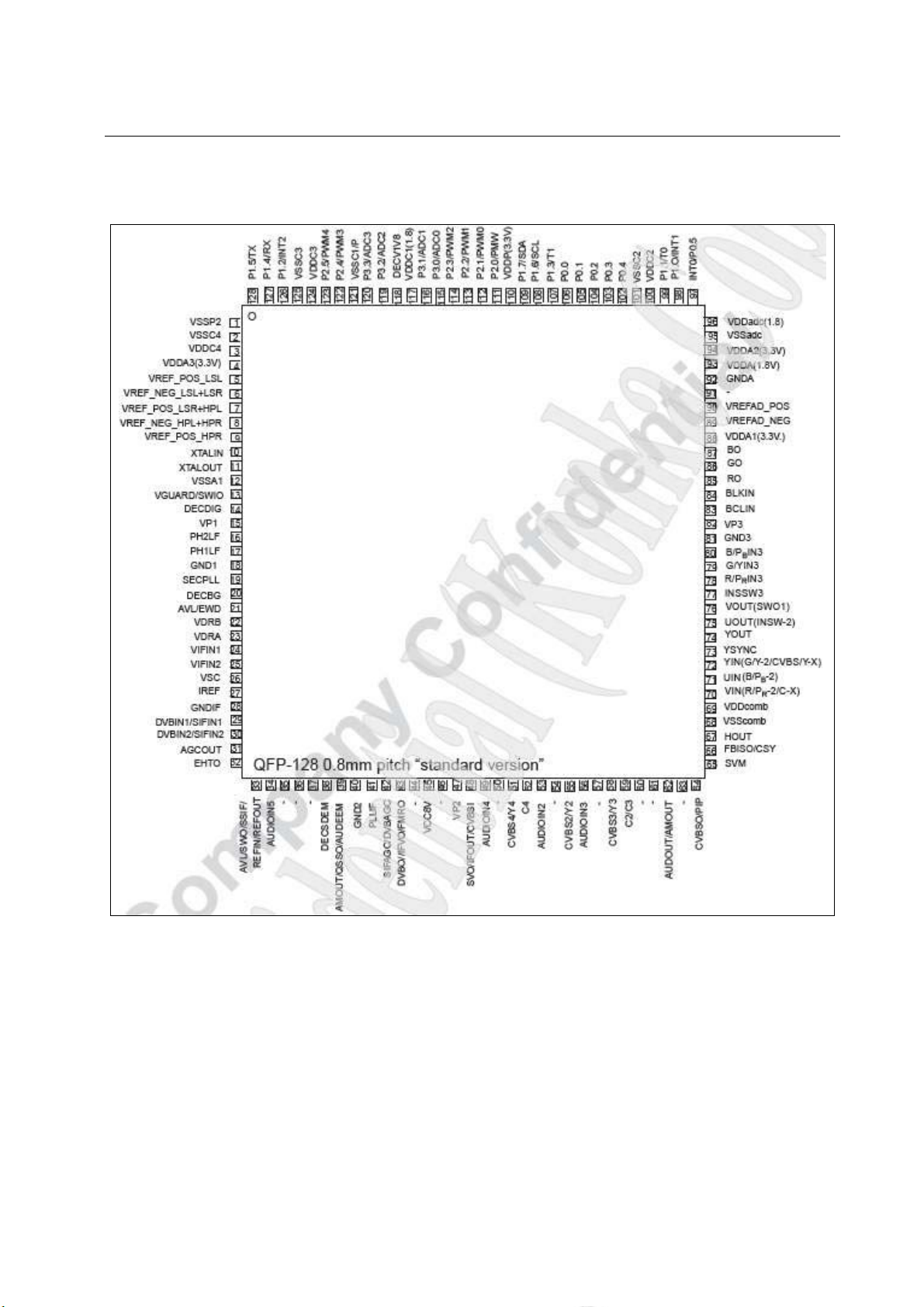
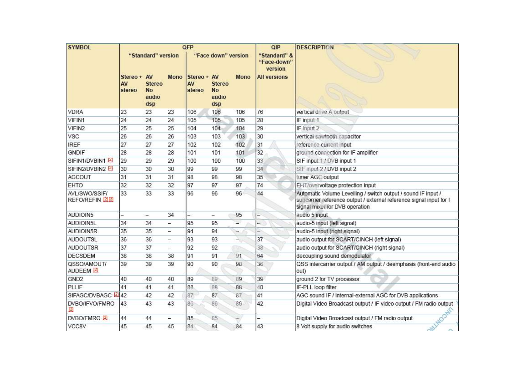
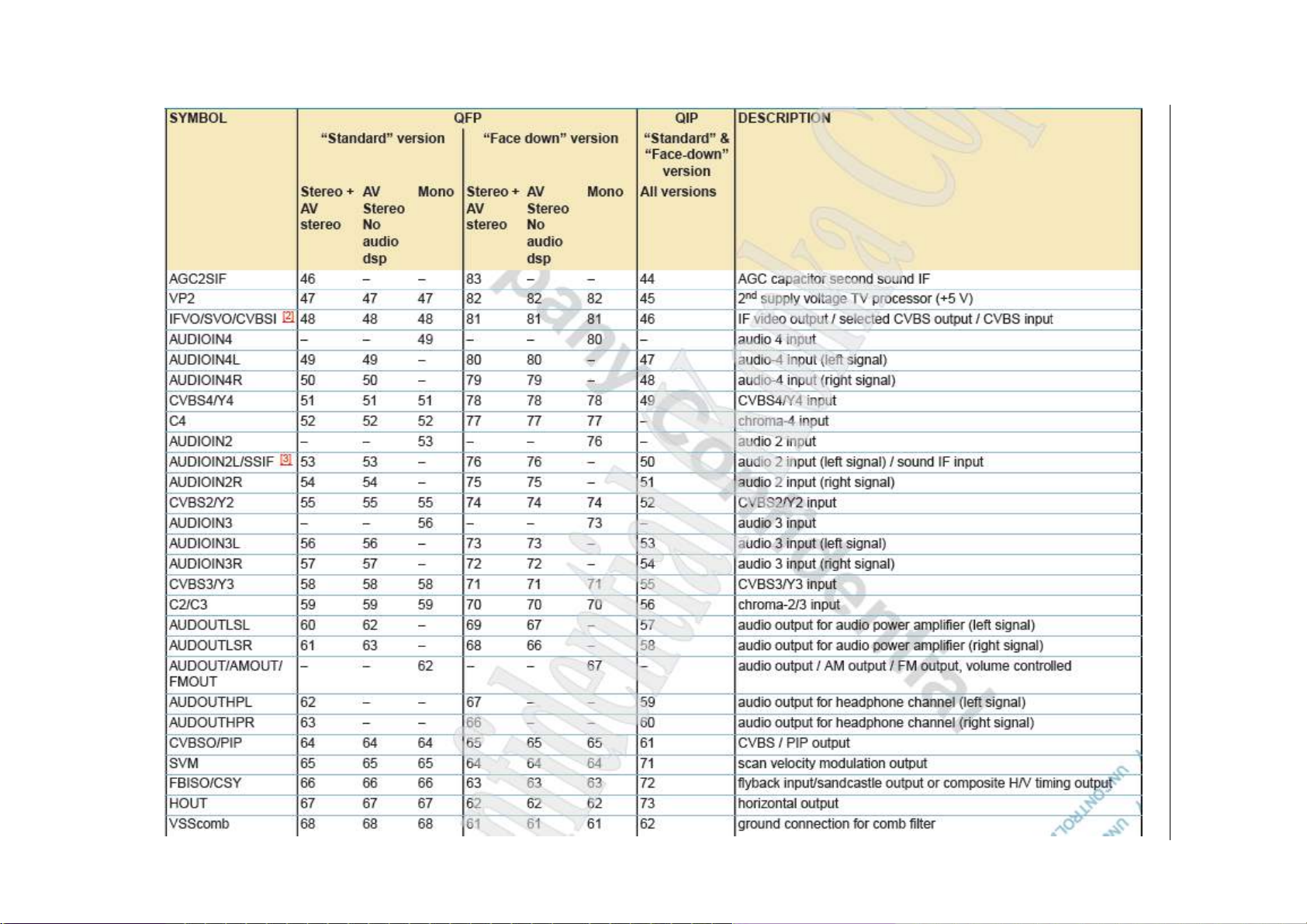
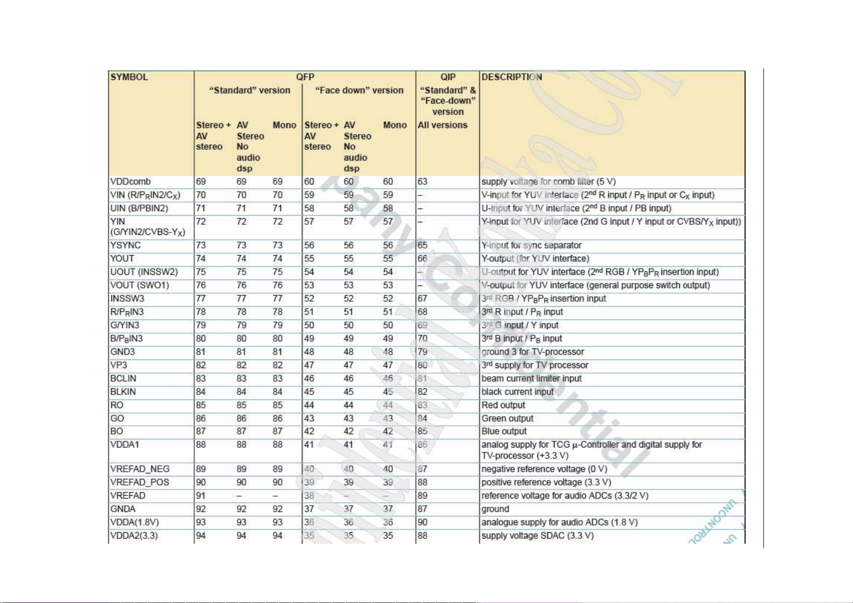
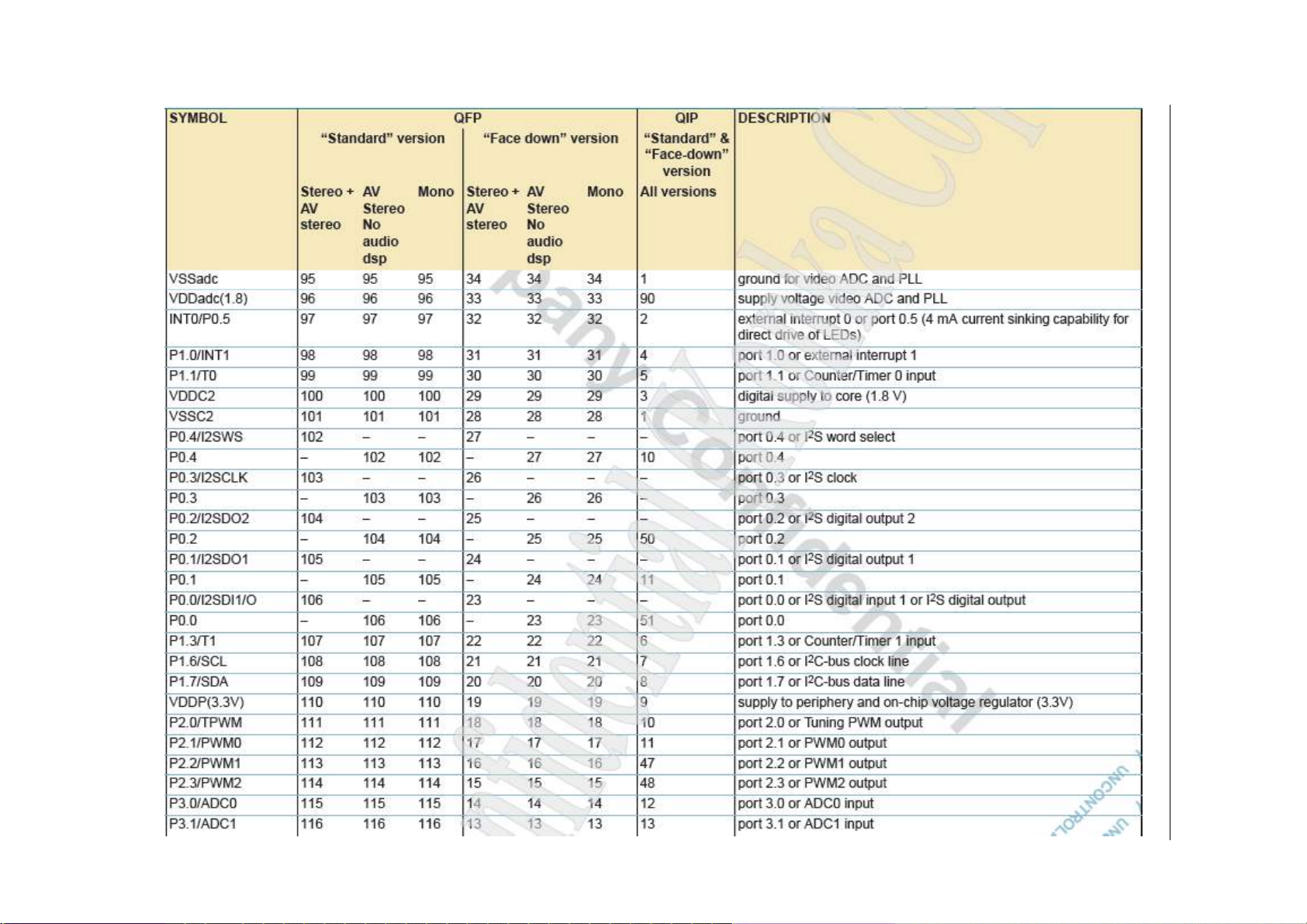
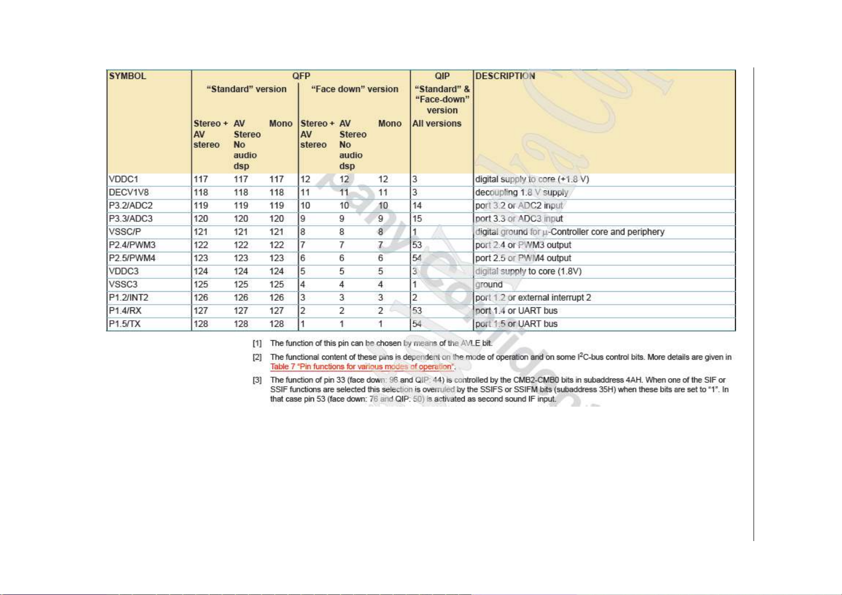
1.5 Pinning information
SERVICE MANUAL TK-A/Q
Pin configuration “mono” versions
27
Page 28
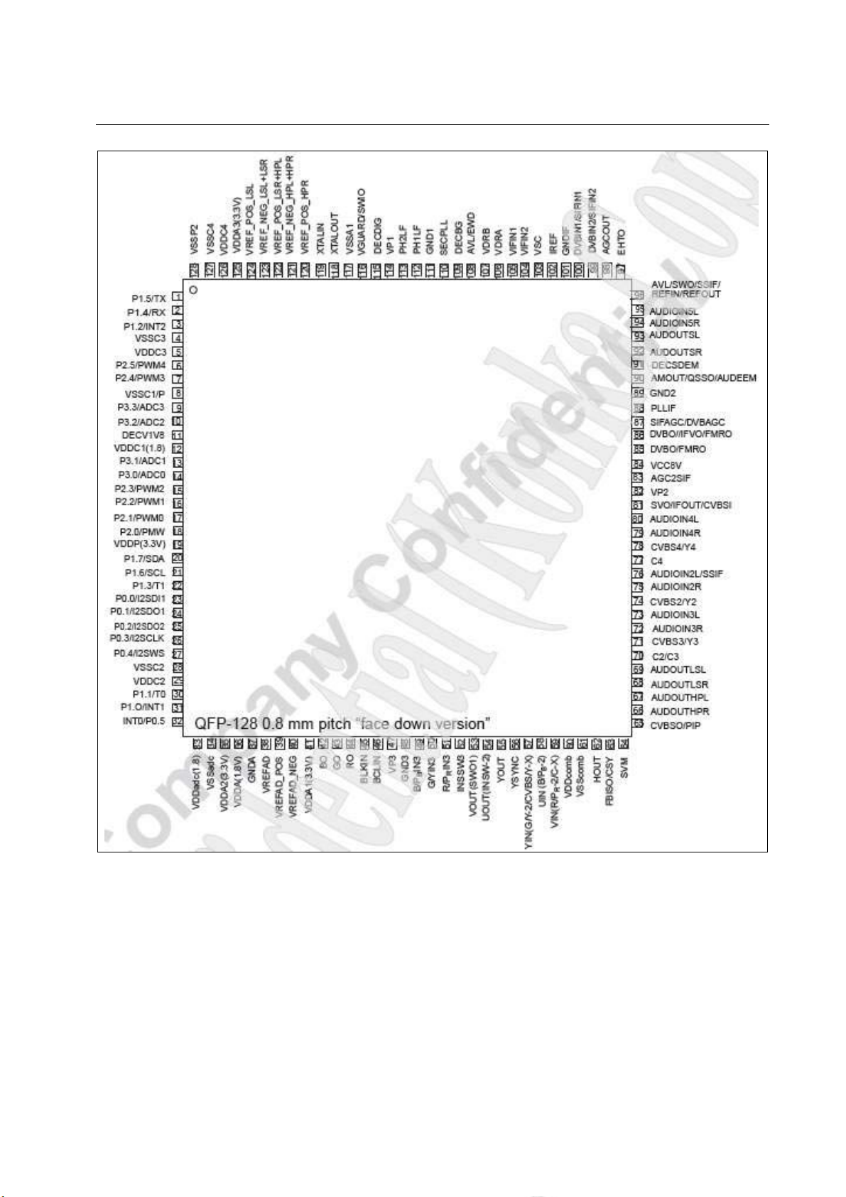
SERVICE MANUAL TK-A/Q
Pin configuration “stereo” and “AV-stereo” versions with Audio DSP
28
Page 29
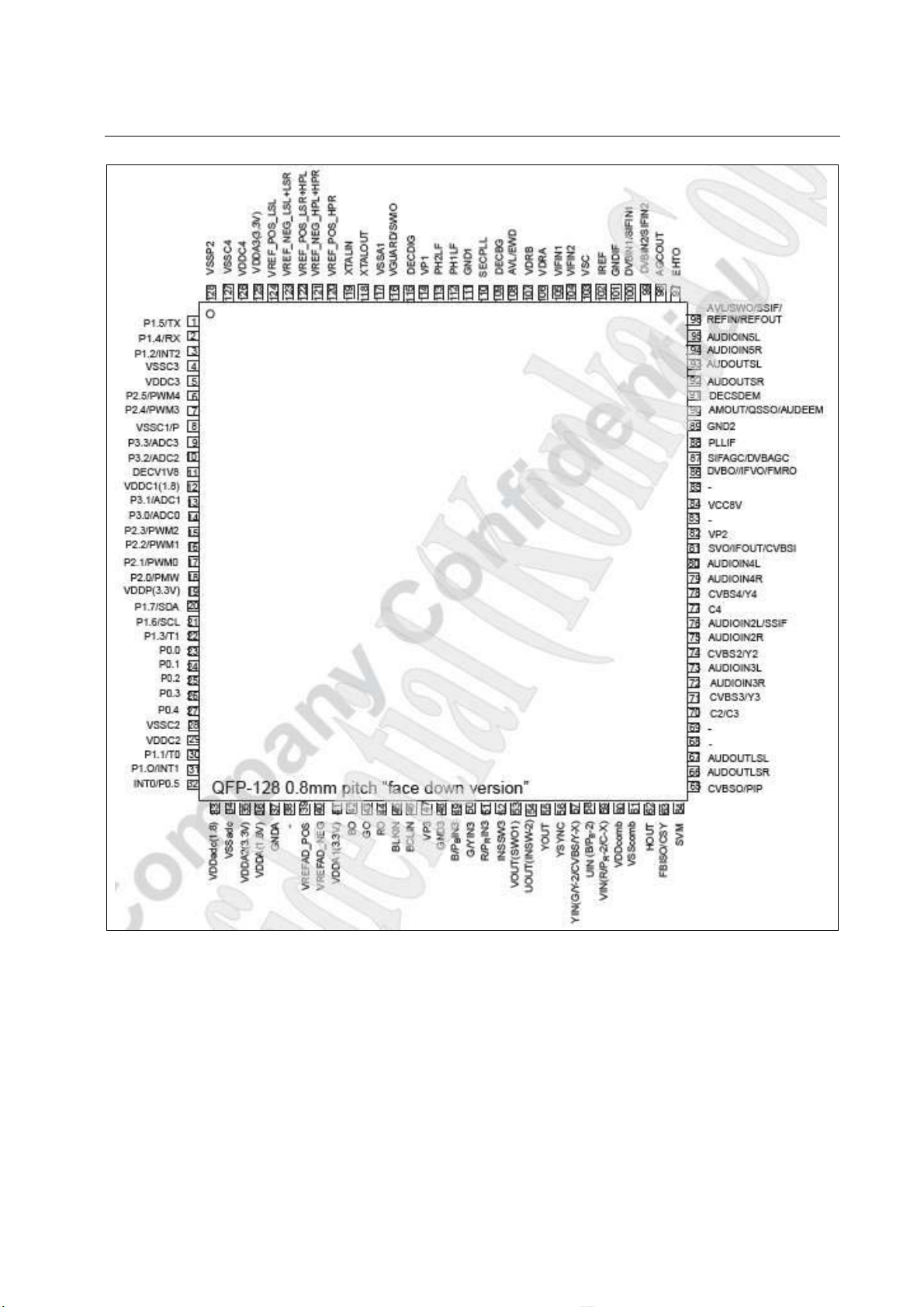
SERVICE MANUAL TK-A/Q
Pin configuration of “AV stereo” versions without Audio DSP
29
Page 30
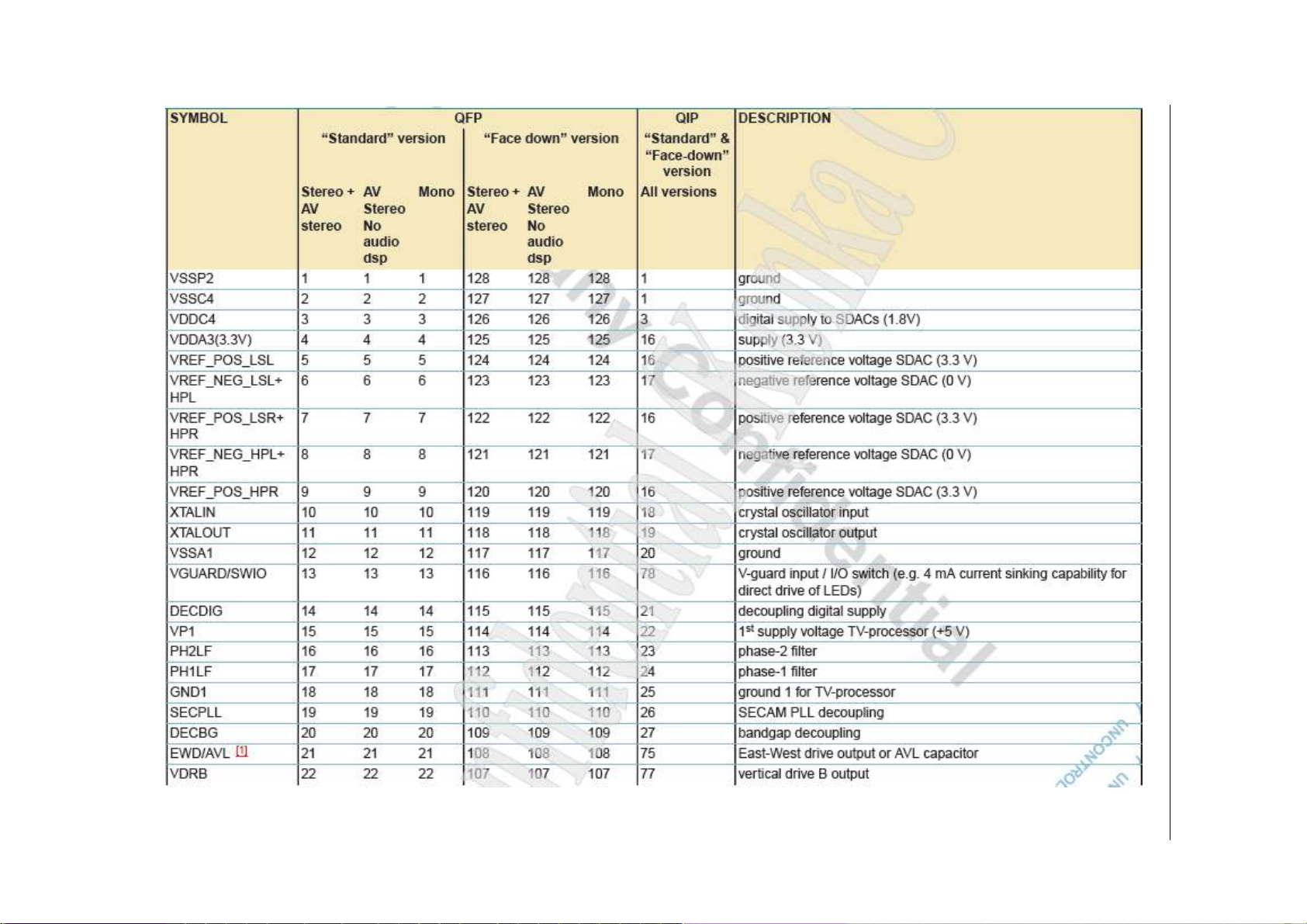
30
SERVICE MANUAL TK-A/Q
Page 31
31
SERVICE MANUAL TK-A/Q
Page 32
32
SERVICE MANUAL TK-A/Q
Page 33
33
SERVICE MANUAL TK-A/Q
Page 34
34
SERVICE MANUAL TK-A/Q
Page 35
35
SERVICE MANUAL TK-A/Q
Page 36

SERVICE MANUAL TK-A/Q
1.6 Power & Reset Management
There are three Power Saving modes, Stand-by, Idle and Power Down, incorporated into the
TCG µ-Controller die. When utilizing either mode, the 3.3V power to the device (VDDP & VDDA)
should be maintained, the 1.8V power to digital core except 80c51 and pads will be switched-off
internally to minimize the leakage current. The internally generated 1.8V will be maintained to
supply the power of 80c51 and pads.
1.6.1 Reset Capabilities
The TCG µ-Controller global power on reset is generated internally hence no external reset
circuitry is required.
Furthermore two additional user reset possibilities are offered:
• a hardware reset via pin P_TMSEL
a software reset via pin P_TMSEL
•
The pin P_TMSEL is in two different ways: for test mode and FLASH/ISP programming
control and as a global reset pin to the TCG µ-Controller. The reset capability is an active high reset
incorporating an internal pull-down. Thus it can be left unconnected in the application. In UOCIII
this pin is connected to the VSP die but the VSP is capable to serve this functionality in a kind of
bypass mode.
The software reset capability is performed using a reset bit inside a SFR register called
ROMBK. This bit is used by the microµ-Controller to reset the following functions / blocks: stereo
sound decoder, RDS, ISP, acquisition, display, display RAM and digital video interface. The
software reset is executed by initially setting the corresponding bit to ‘1’ followed by clearing the bit
to ‘0’. The reset is launched after the falling edge of this process. It takes approximately 200 ms to
complete the internal reset sequence. Please note that of course the micro controller, its peripherals
(e.g. timers) and the program flash are not affected by this reset.
1.6.2 Power Modes
1.6.2.1 Stand-by mode
During Stand-by mode, the Acquisition, Display, RDS, and SSD sections of the device are
disabled. The following functions remain active:
36
Page 37

SERVICE MANUAL TK-A/Q
• 80c51 CPU Core
I2C
•
• RCP (Remote Control Pre-processor)
Timer/Counters
•
• WatchDog Timer
UART, SAD and PWMs
•
To enter Stand-by mode, the STANDBY bit in the ROMBANK register must be set. The status
of all SFRs, internal RAM contents are maintained, as are the device output pin values, but the
contents of Display memory are lost. Since the output values on RGB and VDS are maintained the
display output must be disabled before entering this mode. This mode should be used in conjunction
with both Idle and Power-Down modes.
It is not recommended to enter either the Idle mode or Power-Down mode directly from the
application mode. During Standby mode execution the necessary provisions are executed to safely
enter the subsequent modes and re-cover from them.
1.6.2.2 Idle mode
During Idle mode, Acquisition, Display, RDS, SSD and the CPU sections of the device are
disabled. The following functions remain active:
• I2C
RCP
•
• Timer/Counters
WatchDog Timer
•
• UART, SAD and PWMs
To enter Idle mode the IDL bit in the PCON register must be set. The WatchDog timer must be
disabled prior to entering Idle to prevent the device being reset. It is advice to use the RCP (Remote
Control Pre-processor) during the Idle mode to reduce the false interrupt wake-up of 80c51 in order
to achieve the low power saving mode. The CPU state is frozen along with the status of all SFRs,
internal RAM contents are maintained, as are the device output pin values, but the contents of
Display memory are lost. Since the output values on RGB and VDS are maintained the Display
output must be disabled before entering this mode.
There are three methods available to recover from Idle:
37
Page 38

SERVICE MANUAL TK-A/Q
• Assertion of any enabled interrupt will cause the IDL bit to be cleared by hardware, thus
terminating Idle mode. The interrupt is serviced, and following the instruction RETI, the next
instruction to be executed will be the one after the instruction that put the device into Idle mode.
A second method of exiting Idle is via an Interrupt generated by the SAD DC Compare circuit.
•
When TCG µ-Controller is configured in this mode, detection of an analogue threshold at the input
to the SAD may be used to trigger wake-up of the device i.e. TV Front Panel Key-press. As above,
the interrupt is serviced, and following the instruction RETI, the next instruction to be executed will
be the one following the
instruction that put the device into Idle.
• The third method of terminating idle mode is with a power on reset. Reset defines all SFRs and
Display memory to a pre-defined state, but maintains all other RAM values. Code execution
commences with the program counter set to “0000”.
1.6.2.3 Power down mode
In Power Down mode the XTAL oscillator is running still. The contents of all SFRs and Data
memory are maintained, however, the contents of the Display memory are lost. The port pins
maintain the values defined by their associated SFRs. Since the output values on RGB and VDS are
maintained the Display output must be made inactive before entering Power Down mode.
The power down mode is activated by setting the PD bit in the PCON register. It is advised to
disable the WatchDog timer prior to entering Power down. Recovery from Power-Down takes
several milli-seconds as the oscillator must be given time to stabilize.
There are three methods of exiting power down:
The first method to wake up from Power-Down is to use one of these two external interrupts: EX0
•
and EX1. The interrupt EX2 cannot be used to wake up the system. Since the clock is stopped, these
external interrupts needs to be set level sensitive before entering Power-Down. The interrupt is
serviced, and following the instruction RETI, the next instruction to be executed will be the one
after the instruction that put the device into Power-Down mode.
• A second method to exit Power-Down is via an interrupt triggered by the SAD DC comparator.
This can be used e.g. to trigger a wake-up of the device by TV Front Panel key-press. As above, the
interrupt is serviced, and following the instruction RETI, the next instruction to be executed will be
the one following the instruction that put the device into Power-Down
38
Page 39
SERVICE MANUAL TK-A/Q
• The third method of terminating the Power-Down mode is with a Power On reset. Reset defines all
SFRs and Display memory, but maintains all other RAM values. Code execution commences with
the Program Counter set to “0000”.
1.6.2.4 General recommendations
In power saving application modes where all three external interrupts are required the Idle
mode must be used. The difference between the Power Down mode and the Idle mode in terms of
power is quite small since they only differ in the amount of peripherals kept operational. The
purpose of these peripherals is to provide the interrupt request signals to wake up the micro
controller.
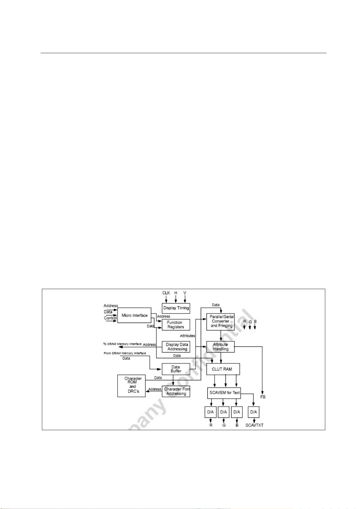
1.7 Display Engine
The display section reads the contents of the Display memory and interprets the
control/character codes. From this information and other global settings, the display produces the
required RGB signals and Video/Data (Fast Blanking) signal for a TV signal processing device.
The display is synchronized to the TV signal processing device by way of Horizontal and
Vertical sync signals generated in UOCIII. From these signals the display timing is derived.
Display Block Diagram
39
Page 40

SERVICE MANUAL TK-A/Q
1.8 Functional Description Video Processor
1.8.1 Vision IF amplifier
The vision IF amplifier can demodulate signals with positive and negative modulation. The
PLL demodulator is completely alignment-free.
The VCO of the PLL circuit is internal and the frequency is fixed to the required value by using
the clock frequency of the TCG mµ-Controller as a reference. The setting of the various frequencies
(e.g. 38, 38.9, 45.75 and 58.75 MHz) can be made via the control bits IFA-IFC in subaddress 2FH.
Because of the internal VCO the IF circuit has a high immunity to EMC interferences.
The output of the AFC detector can be read from output byte 04H and has a resolution of 7 bits
(25 kHz per step). By means of this information a fast tuning algorithm can be designed.
The IC contains a group delay correction circuit which can be switched between the BG and a
uncompensated group delay response characteristic. This has the advantage that in multi-standard
receivers no compromise has to be made for the choice of the SAWfilter. This group delay
correction is realised for the demodulated CVBS output signal. The IC contains in addition a sound
trap circuit with a switchable centre frequency.
1.8.2 Digital Broadcast reception
Apart from processing analogue TV signals, the IF circuit can also preprocess digital TV
signals before they are sent to a digital signal processor. These signals have to be supplied to the
sound IF inputs. In this mode the IF reference frequency is fixed at 43.008 or 49.152 MHz. It is also
possible to supply an external reference signal to demodulator. The demodulator multiplies the
incoming signal with the fixed oscillator frequency. The mixed down signal is low pass filtered to
obtain a I-signal. The “Stereo” and “AV Stereo” versions have a differential output, however, it is
possible to use a single-ended output. The various output signal conditions can be set by means of
the IFO2-IFO0 bits in subaddress 31H (see also Table 128). The “Mono” versions have a
single-ended output.
The AGC has two modes of operation: the internal mode in which the IC sets the gain with its
own reference and an external mode in which the gain can be controlled with an external circuit. In
the second case the SIFAGC pin is used as an input to control the IF gain with an external circuit.
40
Page 41

SERVICE MANUAL TK-A/Q
1.8.3 QSS Sound circuit
The sound IF amplifier is similar to the vision IF amplifier and has an external AGC
decoupling capacitor.
The single reference QSS mixer is realised by a multiplier. In this multiplier the SIF signal is
converted to the intercarrier frequency by mixing it with the regenerated picture carrier from the
VCO. The mixer output signal is supplied to the output via a high-pass filter for attenuation of the
residual video signals. With this system a high performance hi-fi stereo sound processing can be
achieved.
The AM sound demodulator is realised by a multiplier. The modulated sound IF signal is
multiplied in phase with the limited SIF signal. The demodulator output signal is supplied to the
output via a low-pass filter for attenuation of the carrier harmonics.
Switching between the QSS output and AM output is made by means of the AM bit in
subaddress 33H.
1.8.4 FM demodulator
The FM demodulator is realised as narrow-band PLL with internal loop filter, which provides
the necessary selectivity without using an external band-pass filter. To obtain a good selectivity a
linear phase detector and a constant input signal amplitude are required. For this reason the
intercarrier signal is internally supplied to the demodulator via a gain controlled amplifier and AGC
circuit. To improve the selectivity an internal bandpass filter is connected in front of the PLL circuit.
The nominal frequency of the demodulator is tuned to the required frequency (4.5/5.5/6.0/6.5
MHz) by means of a calibration circuit which uses the clock frequency of the TCG11 mµ-Controller
as a reference. It is also possible to frequencies of 4.72 and 5.74 MHz so that a second sound
channel can be demodulated. In the latter application an external bandpass filter has to be applied to
obtain sufficient selectivity (the sound input can be activated by means of the setting of
CMB2-CMB0 bits in subaddress 4AH). The setting to the wanted frequency is realised by means of
the control bits FMA, FMB and FMC in the control bit 33H.
From the output status bytes it can be read whether the PLL frequency is inside or outside the
window and whether the PLL is in lock or not. With this information it is possible to make an
automatic search system for the incoming sound frequency. This can be realized by means of a
software loop which switches the demodulator to the various frequencies and then select the
41
Page 42

SERVICE MANUAL TK-A/Q
frequency on which a lock condition has been found.
The amplitude deemphasis output signal changed with 6 dB by means of the AGN bit. In this
way output signal differences between the 4.5 MHz standard (frequency deviation ±25 kHz) and the
other standards (frequency deviation ±50 kHz) can be compensated.
1.8.5 FM radio mode
The internal FM demodulator can also be used for the demodulation of FM radio signals. This
mode is activated by the FMR bit (subaddress 34H). Depending on the UOCIII version, the mono
demodulator as well as the stereo demodulator can be used for FM radio. Both demodulators can
also be used simultaneously, so switching between the demodulators is an option and RDS
demodulation can also be carried out.
There are two FM-radio options, depending on the tuner. The first one uses an optimized tuner
with 10.7 MHz output. The tuner output signal can be filtered and applied to the SSIF input. The
SSIF frequency of the mono demodulator can be set by the FMD bit. In case of using the stereo
demodulator one have to set the ‘STDSEL’ register. The second option is the FM radio eco (nomy)
using a normal multistandard tuner + an extra Radio I.F. SAW filter. In this case the I.F.
demodulator has to be set to one of the fixed frequencies (43.008 MHz or 49.152 MHz) by the IFA
-IFE bits in subaddress 31H. The I.F. centre frequency depends on the I.F. downmix frequency and
the FM demodulator settings. The bandwidth of the RIF filter should be between 200 and 300 KHz
for proper channel selectivity. A common QSS sound SAW filter with 800 KHz bandwidth is too
wide. In the FM radio eco mode the SSIF output signal can be supplied to the output pins (FMRO)
for external filtering by setting the IFO2- IFO0 bits in subaddress 31H.
The SS IF bit can be either pin 33 or pin 53 (pins 96 or 76 respectively for the “face down”
version). The selection is made by means of the CMB2-CMB0, SSIFS and SSIFM bits.
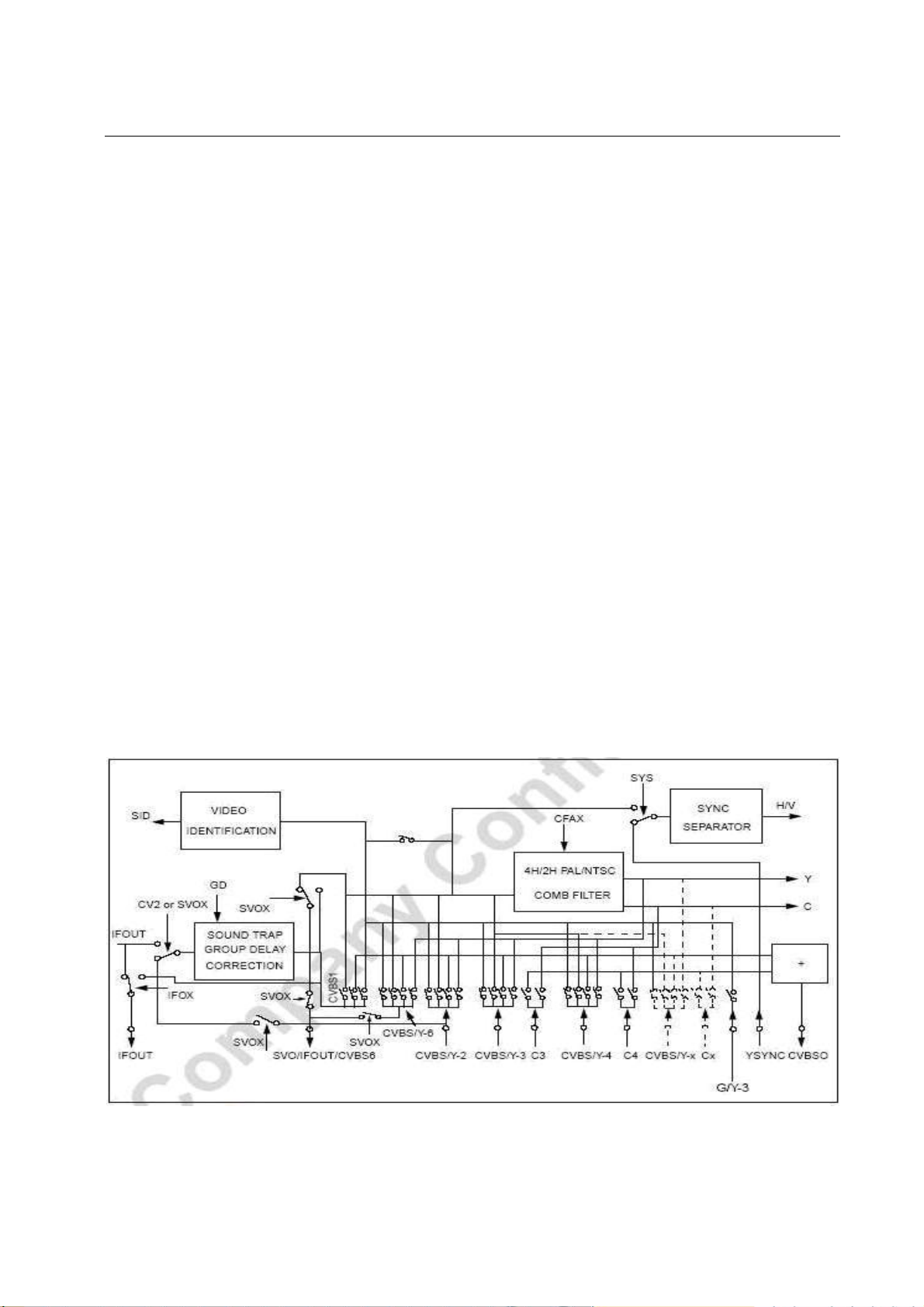
1.8.6 CVBS and Y/C input signal selection
The ICs have 3 inputs for external CVBS signals. All CVBS inputs can be used as Y input for
the insertion of Y/C signals. However, the CVBS(Y)2 input has to be combined with the C3 input. It
is possible to add and extra CVBS(Y/C) input via the pins which are intended to be used for YUV
interface (or RGB/YPBPR input). The selection of this additional CVBS(Y/C) input is made via the
YC bit. The CVBS selector has one independently switchable output. The switch configuration is
42
Page 43
SERVICE MANUAL TK-A/Q
given in Figure 72. The choice of the various modes can be made via the INA-IND bits in
subaddress 38H.
The function of the IFVO/SVO/CVBS6 pin is determined by the SVO1/SVO0 bits. When used
as output a selection can be made between the IF video output signal or the selected CVBS signal
(monitor out). This pin can also be used as additional CVBS input. In the input selector this signal is
indicated as CVBS/Y-6 (see Figure 72). The CVBS/Y-6 input has to be combined with the C4 input.
The selection of the CVBS/Y-6 signal is valid only at the SVO1/SVO0 setting 1/0.
It is possible to use the group delay and sound trap circuit for the CVBS2 signal (via the CV2
bit).
For the CVBS(Y/C) inputs the circuit can detect whether a CVBS or Y/C signal is present on
the input. The result can be read from the status register (YCD bit in subaddress 03H) and this
information can be used to put the input switch in the right position (by means of the INA-IND bits
in subaddress 38H). The Y/C detector is only active for the CVBS(Y)3/C3, CVBS(Y)4/C4 and
CVBS(Y)x/Cx inputs. It is not active for the CVBS(Y)2/C3 and CVBS(Y)6/C4 inputs.
The video ident circuit can be connected to all video input signals. This ident circuit is
independent of the synchronisation and can be used to switch the time-constant of the horizontal
PLL depending on the presence of a video signal (via the VID bit). In this way a very stable OSD
can be realised. The result of the video ident circuit can be read from the output bit SID (subaddress
00).
CVBS switch
43
Page 44

SERVICE MANUAL TK-A/Q
1.8.7 Synchronisation circuit
The IC contains separator circuits for the horizontal and vertical sync pulses. To obtain an
accurate timing of the displayed picture the input signal of the sync separator is not derived from the
various CVBS/Y or RGB/YPBPR inputs but from the YOUT pin. For this reason the YOUT pin
must be capacitively coupled to the YSYNC pin. The delay between the various inputs and the
YOUT signal can have rather large differences (e.g. comb filter active or not). By choosing the
YOUT signal as input signal for the sync separator these delays have no effect on the picture
position. Only for RGB signals without sync on green the input of the sync separator has to be
connected to one of the CVBS inputs. This selection is made by means of the SYS bit.
The horizontal drive signal is obtained from an internal VCO which is running at a frequency
of 25 MHz. This oscillator is stabilised to this frequency by using the clock signal coming from the
reference oscillator of the TCG mµ-Controller.
To obtain a stable On-Screen-Display (OSD) under all conditions it is important that the first
control loop is switched off or set to low gain when no signal is available at the input. The input
signal condition is detected by the video identification circuit. The video identification circuit can
automatically switch first control loop to a low gain when no input signal is available. This mode is
obtained when the VID bit is set to “0”. When the VID bit is “1” the mode of the first control loop
can be switched by means of the FOA/FOB or POC bits.
For a good performance during normal TV reception (display of the front-end signal) various
connections are active between the vision IF amplifier and the synchronization circuit (e.g. gating
pulses for the AGC detector and noise gating of the sync separator). These connections are not
allowed when external video signals are displayed. The switching of these connections can be
coupled to the input signal selection bits (INA-IND). This mode is obtained when the VDXEN bit is
“0”. Due to the input signal selector configuration it is possible that the internal CVBS signal is
available on one of the other CVBS inputs. In this condition the connections between the vision IF
amplifier and the synchronisation circuit can be switched on and off by means of the VDX bit. The
VDXEN bit must be set to “1” for this mode.
The vertical synchronisation is realised by means of a divider circuit.
1.8.8 Horizontal and vertical drive
The horizontal drive is switched on and off via the soft start/stop procedure. The soft start
44
Page 45

SERVICE MANUAL TK-A/Q
function is realised by means of variation of the TON of the horizontal drive pulses. During the
soft-stop period the horizontal output frequency is doubled resulting in a reduction of the EHT so
that the picture tube capacitance can easily be discharged. In addition the horizontal drive circuit has
a ‘low-power start-up’ function.
The vertical ramp generator needs an external resistor and capacitor. For the vertical drive a
differential output current is available. The outputs must be DC coupled to the vertical output stage.
The IC has the following geometry control functions:
Vertical amplitude
•
• Vertical slope
• S-correction
• Vertical shift
• Vertical zoom
• Vertical scroll
• Vertical linearity correction. When required the linearity setting for the upper and lower part of the
screen can have a different setting.
• Horizontal shift
• EW width
• EW parabola width
• EW upper and lower corner parabola correction
• EW trapezium correction
• Horizontal parallelogram and bow correction.
When the vertical amplitude is compressed (zoom factor <1) it is still possible to display the
black current measuring lines in the overscan. This function is activated by means of the bit OSVE
in subaddress 40H.
The vertical guard input is combined with an I/O function. The following functions can be
realised with this pin:
• Just vertical guard input.
• Combination of vertical guard and LED drive output. In this condition the output is high-ohmic
during the vertical retrace (1 ms) so that the vertical guard pulse can be detected.
• Single ended output switch
• Input port
45
Page 46

SERVICE MANUAL TK-A/Q
The functionality of this pin is controlled by the VGM1/0 and LED bits.
When the East-West geometry function is not required (e.g. for 90° picture tubes) the EW
output pin can be used for the connection of the AVL capacitor. This function is chosen by means of
the AVLE bit.
The UOCIII devices can also be used as input processor for 100 Hz or LCD TV receivers. In
that case the deflection drive signals are not required. For these applications, H/V timing signal can
be obtained from the H-drive and VDRB output pins. The polarity of these pulses is negative. For
the H-output a pull-up resistor is required. The sandcastle signal will be available on the FBISO pin.
This mode is activated by means of the LCD bit (subaddress 4AH). A change of the LCD bit is
possible only in the stand-by mode (STB = 0).
1.8.9 Chroma, luminance and feature processing
Some versions contain a 4H/2H (2D) adaptive PAL/NTSC comb filter. The comb filter is
automatically activated when standard CVBS signals are received. A signal is considered as
“standard signal” when a PAL or NTSC signal is identified and when the vertical divider is in the
modes ‘standard narrow window’ or ‘standard TV norm’.For non-standard signals and for SECAM
signals the comb filter is bypassed and the signal is filtered by means of bandpass and trap filters.
The chroma band-pass and trap circuits (including the SECAM cloche filter) are realized by
means of internal filters and are tuned to the right frequency by comparing the tuning frequency
with the reference frequency of the colour decoder.
The circuit contains the following picture improvement features:
• Peaking control circuit. The peaking function can be activated for all incoming CVBS, Y/C and
RGB/YPBPR signals. Various parameters of the peaking circuit can be adapted by means of the
I2C-bus. The main parameters are:
– Peaking centre frequency (via the PF1/PF0 bits in subaddress 19H).
– Ratio of positive and negative peaks (via the RPO1/RPO0 bits in subaddress 47H). The peaks in
the direction “white” are the positive peaks.
– Ratio of pre- and aftershoots (via the RPA1/RPA0 bits in subaddress 47H).
• Video dependent coring in the peaking circuit. The coring can be activated only in the low-light
parts of the screen. This effectively reduces noise while having maximum peaking in the bright parts
of the picture.
46
Page 47

SERVICE MANUAL TK-A/Q
• Black stretch. This function corrects the black level for incoming signals which have a difference
between the black level and the blanking level. The amount of stretching (A-A in Fig. 105) and the
minimum required back ground to activate the stretching can be set by means of the I2C-bus
(BSD/AAS in subaddress 45H).
• Gamma control. When this function is active the transfer characteristic of the luminance amplifier
is made non-linear. The control curve can be adapted by means of I2C-bus settings (see Fig. 107). It
is possible to make the gamma control function dependent on the picture content (Average Picture
Level, APL). The effect is illustrated in Fig. 108. Previously this function was mentioned under the
name “white stretch function”.
• Blue-stretch. This circuit is intended to shift colour near ‘white’ with sufficient contrast values
towards more blue to obtain a brighter impression of the picture.
• Dynamic skin tone (flesh) control. This function is realised in the YUV domain by detecting the
colours near to the skin tone.
• Scan-Velocity modulation output. Also the SVM function can be activated for all incoming CVBS,
Y/C and RGB/YPBPR signals. The delay between the RGB output signals and the SVM output
signal can be adjusted (by means of the SVM2-SVM0 bits in subaddress 48H) so that an optimum
picture performance can be obtained. Furthermore a coring function can be activated. It is possible
to generate Scan Velocity Modulation drive signals during the display of ‘full screen’ teletext (not in
mixed mode). Another feature is that the SVM output signal can be made dependent on the
horizontal position on the screen (parabola on the SVM output).
The effect of the various features can de demonstrated by means of the ‘split-screen’ mode.
When the TV receiver is switched to this mode the features are switched on in the left half of the
picture and switched off in the right half of the picture or vice versa. It is possible to add a signal
blanking in the middle of the screen. The features that are switched on and off are: peaking, scan
velocity modulation, black stretch, gamma control, DC transfer ratio, blue stretch, dynamic skin
tone control, tint on U/V and soft clipping.
1.8.10 Colour decoder
The ICs decode PAL, NTSC and SECAM signals. The PAL/NTSC decoder does not need
external reference crystals but has an internal clock generator which is stabilised to the required
frequency by using the clock signal from the reference oscillator of the TCG mµ-Controller.
47
Page 48

SERVICE MANUAL TK-A/Q
Under bad-signal conditions (e.g. VCR-playback in feature mode), it may occur that the colour
killer is activated although the colour PLL is still in lock. When this killing action is not wanted it is
possible to overrule the colour killer by forcing the colour decoder to the required standard and to
activate the FCO-bit (Forced Colour On) in subaddress 3CH. The sensitivity of the colour decoder
for PAL and NTSC can be increased by means of the setting of the CHSE1/CHSE0 bits in
subaddress 3CH.
The Automatic Colour Limiting (ACL) circuit (switchable via the ACL bit in subaddress 3BH)
prevents that oversaturation occurs when signals with a high chroma-to-burst ratio are received. The
ACL circuit is designed such that it only reduces the chroma signal and not the burst signal. This has
the advantage that the colour sensitivity is not affected by this function.
The SECAM decoder contains an auto-calibrating PLL demodulator which has two references,
viz: the divided reference frequency (obtained from the mµ-Controller) which is used to tune the
PLL to the desired free-running frequency and the bandgap reference to obtain the correct absolute
value of the output signal. The VCO of the PLL is calibrated during each vertical blanking period,
when the IC is in search or SECAM mode. The frequency offset of the B-Y demodulator can be
reduced by means of the SBO1/SBO0 bits in subaddress 3CH.
The base-band delay line is integrated. In devices without CVBS comb filter this delay line is
also active during NTSC to obtain a good suppression of cross colour effects. The demodulated
colour difference signals are internally supplied to the delay line. The baseband comb filter can be
switched off by means of the BPS bit (subaddress 3CH).
The subcarrier output is combined with a 3-level output switch (0 V, 2.1 V and 4.5 V). The
output level and the availability of the subcarrier signal is controlled by the CMB2-CMB0 bits.
1.8.11 RGB output circuit
In the RGB control circuit the signal is controlled on contrast, brightness and saturation. The IC
has a YUV interface so that additional picture improvement ICs can be applied. To compensate
signal delays in the external YUV path the clamp pulse in the control circuit can be shifted by means
of the CLD bit in subaddress 44H. When the YUV interface is not required some of the pins can be
used for the insertion of RGB/YPBPR signals or as additional CVBS(Y)/C input. When the YUV
interface is not used one of the pins (VOUT) is transferred to general purpose output switch (SWO1).
The IC has also a YUV interface to the digital die. Via this loop digital features like “double
48
Page 49

SERVICE MANUAL TK-A/Q
window” are added.
A tint control is available for the base-band U/V signals. For this reason this tint control can be
activated for all colour standards. The signals for OSD and text are internally supplied to the control
circuit. The output signal has an amplitude of about 1.2 V black-to-white at nominal input signals
and nominal settings of the various controls.
To obtain an accurate biasing of the picture tube the ‘Continuous Cathode Calibration’ system
has been included in these ICs. The system is slightly adapted compared with the previous circuits.
In the new configuration the cut-off level of the picture tube is controlled with a continuous loop
whereas the correction of the amplitude of the output signals is realised by means of a digital loop.
As a consequence the current measurement can be controlled from the m-Processor. The value of
the “high current” in the CCC loop can be chosen via the SLG0 and SLG1 bits (subaddresses 42H
and 46H). The gain control in the 3 RGB channels is realised by means of 7-bit DACs. The total
gain control range is ±6 dB. The change in amplitude at the cathodes of the picture tube for one LSB
is about 1.1 VP-P. The setting of the control DAC is determined by the following registers:
• The white point setting of the R, G and B channel in subaddress 20H to 22H. This register has a
resolution of 6 bits and the control range in output signal amplitude is ±3 dB.
• The cathode drive setting (CL3-CL0 in subaddress 42H). This setting is valid for all channels, the
resolution is 4 bits and the control range is ±3 dB.
• The gain setting of the R, G and B channel. During switch on this register is loaded with the preset
gain setting of subaddress 23H to 25H and when necessary it will be adapted by the CCC control
loop. These registers have a resolution of 7 bits.
The setting of the gain registers of the 3 channels can be stored during switch off and can be
loaded again during switch-on so that the drive conditions are maintained.
When required the operation of the CCC system can be changed into a one-point black current
system. The switching between the 2 possibilities is realised by means of the EGL bit (EGL = 0) in
subaddress 42H. When used as one-point control loop the system will control the black level of the
RGB output signals to the ‘low’ reference current and not on the cut off point of the cathode. In this
way spreads in the picture tube characteristics will not be taken into account. In this condition the
settings of the “white point control registers” (subaddress 20H - 22H) and the “cathode drive level
bits” (CL3 - CL0 in subaddress 42H) are added to the settings of the RGB preset gain registers
(subaddress 23H - 25H).
49
Page 50

SERVICE MANUAL TK-A/Q
A black level off-set can be made with respect to the level which is generated by the black
current stabilization system. In this way different colour temperatures can be obtained for the bright
and the dark part of the picture. The black level control is active on the Red and the Green output
signal. It is also possible to control the black level of the Blue and the Green output signal (OFB bit
= 1).
In the Vg2 adjustment mode (AVG = 1) the black current stabilization system checks the
output level of the 3 channels and indicates whether the black level of the highest output is in a
certain window (WBC-bit) or below or above this window (HBC-bit). This indication can be read
from the status byte 01 and can be used for automatic adjustment of the Vg2 voltage during the
production of the TV receiver. During this test the vertical scan remains active so that the indication
of the 2 bits can be made visible on the TV screen.
The control circuit contains a beam current limiting circuit and a peak white limiting circuit.
The control is realised by means of a reduction of the contrast and brightness control settings. The
way of control (first contrast and then brightness or contrast and brightness in parallel) can be
chosen by means of the CBS bit (subaddress 44H). The peak white level is adjustable via the
I2C-bus.
To prevent that the peak white limiting circuit reacts on the high frequency content of the video
signal a low-pass filter is inserted in front of the peak detector. The circuit also contains a
soft-clipper which prevents that the high frequency peaks in the output signal become too high. The
difference between the peak white limiting level and the soft clipping level is adjustable via the
I2C-bus in a few steps.
During switch-off of the TV receiver a fixed beam current is generated by the black current
control circuit. This current ensures that the picture tube capacitance is discharged. During the
switch-off period the vertical deflection can be placed in an overscan position so that the discharge
is not visible on the screen.
A wide blanking pulse can be activated in the RGB outputs by means of the HBL bit in
subaddress 43H. The timing of this blanking can be adjusted by means of the WBF/R bits in
subaddress 26H. In the LCD mode (AKB = 1 and LCD = 1) the wide blanking can also be activated.
1.9 Functional Description Sound Processor
The TV Sound Processor is a digital TV sound processor for analog multi-channel sound
50
Page 51

SERVICE MANUAL TK-A/Q
systems in TV sets. It is based on a 24 bit DSP and designed to support several applications.
A new easy-to-use control concept was implemented for easiest configuration programming of
the very complex functionality of the TV Sound Processor. Pre-defined setups are available for all
implemented sound processing modes. A loudspeaker switching concept allows it to adapt the
pre-defined setups to the specific loudspeaker application.The built-in intelligence for pre-defined
standards and Auto Standard Detection (ASD) allows an easy setup of the demodulator and decoder
part.
The control concept for the audio processor is based on the following new features:
• Pre-defined setups for the sound processing modes like Dolby® Pro Logic® and Virtual Dolby®
Surround (422, 423)
• Flexible configuration of audio outputs to the loudspeaker configuration with an additional output
crossbar.
• Master volume function
The control concept for the demodulator and decoder (DEMDEC) is based on the following
new features:
• Easy demodulator setup for all implemented standards with Demodulator and Decoder Easy
Programming (DDEP) for a pre-selected standard or combined with Auto Standard Detection (ASD)
for automatic detection of a transmitted standard
• Automatic decoder configuration and signal routing depending on the selected or detected standard
• FM overmodulation adaptation option to avoid clipping and distortion.
51
Page 52
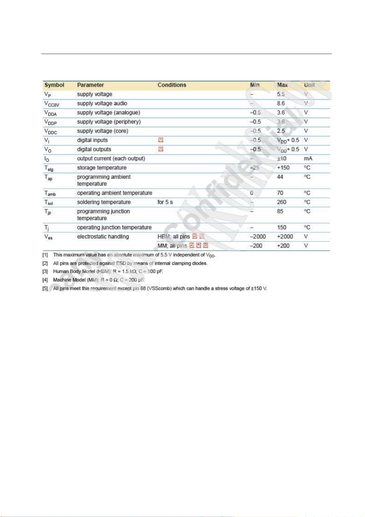
1.10 Limitting values
SERVICE MANUAL TK-A/Q
52
Page 53

SERVICE MANUAL TK-A/Q
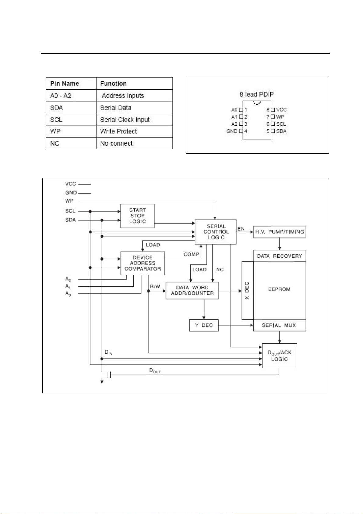
2. EEPROM 24C16 (N602)
2.1 Features
• Write Protect Pin for Hardware Data Protection
– Utilizes Different Array Protection Compared to the AT24C16A
• Low-voltage and Standard-voltage Operation
– 2.7 (VCC = 2.7V to 5.5V)
• Internally Organized 2048 x 8 (16K)
• 2-wire Serial Interface
• Schmitt Trigger, Filtered Inputs for Noise Suppression
• Bi-directional Data Transfer Protocol
• 400 kHz (2.7V) Clock Rate for AT24C16A
• 16-byte Page Write Modes
• Partial Page Writes are Allowed
• Self-timed Write Cycle (10 ms Max)
• High Reliability
– Endurance: One Million Write Cycles
– Data Retention: 100 Years
• Automotive Grade, Extended Temperature and Lead-Free Devices Available
• 8-lead PDIP Packages
2.2 Description
The AT24C16A provides 16384 bits of serial electrically erasable and programmable read only
memory (EEPROM) organized as 2048 words of 8 bits each. In the AT24C16A, the 16K is
internally organized with 128 pages of 16 bytes each. Random word addressing requires an 11-bit
data word address.
The device is optimized for use in many industrial and commercial applications where low
power and low voltage operation are essential. The AT24C16A is available in space saving 8-lead
PDIP package and is accessed via a 2-wire serial interface. In addition, the AT24C16A is available
in 2.7V (2.7V to 5.5V) supply.
53
Page 54
2.3 Pin Configurations
SERVICE MANUAL TK-A/Q
2.4 Block Diagram
54
Page 55
2.5 Pin Description
SERVICE MANUAL TK-A/Q
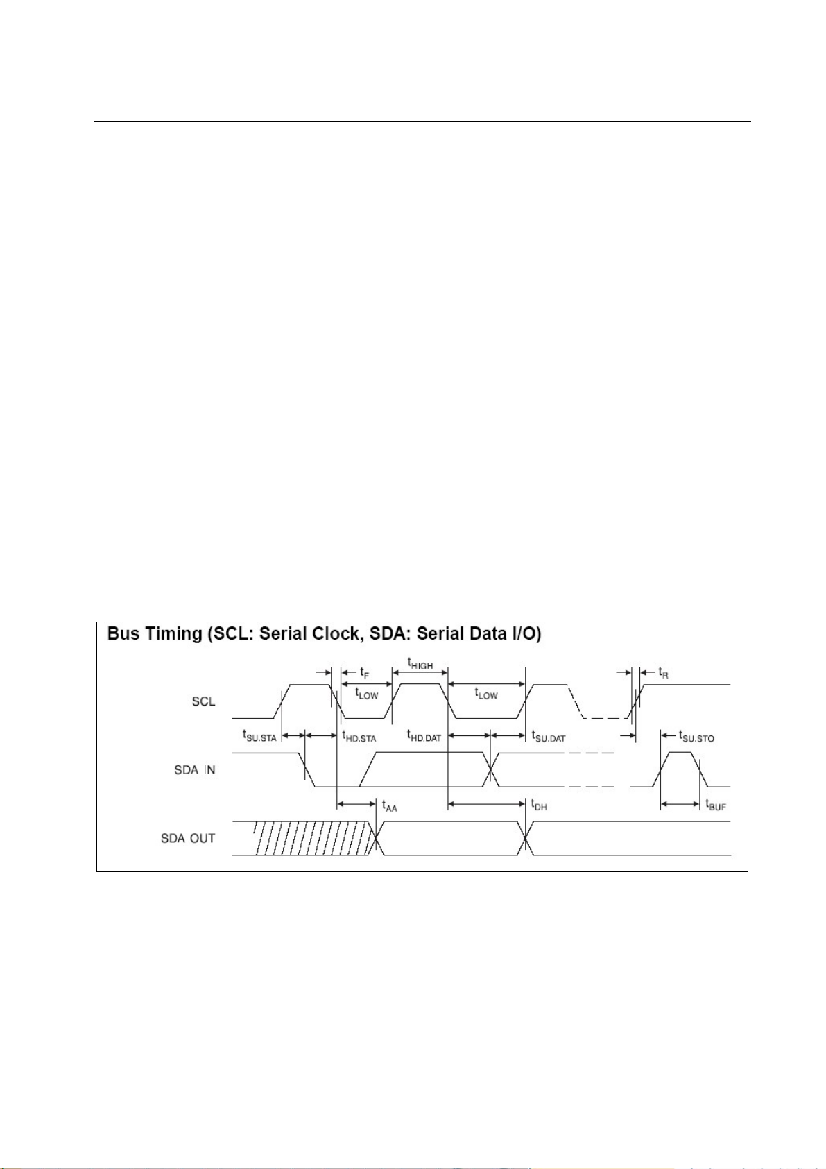
SERIAL CLOCK (SCL):
The SCL input is used to positive edge clock data into each EEPROM
device and negative edge clock data out of each device.
SERIAL DATA (SDA):
The SDA pin is bidirectional for serial data transfer. This pin is open-drain
driven and may be wire-ORed with any number of other open-drain or open collector devices.
DEVICE/PAGE ADDRESSES (A2, A1, A0):
The A2, A1 and A0 pins are device address inputs.
The AT24C16A does not use the device address pins, which limits the number of devices on a
single bus to one. The A0, A1 and A2 pins are no-connects.
WRITE PROTECT (WP): The AT24C16A has a Write Protect pin that provides hardware data
protection. The Write Protect pin allows normal read/write operations when connected to ground
(GND). When the Write Protect pin is connected to VCC, the write protection feature is enabled and
operates as shown in the following table.
2.6 Device Operation
Clock and Data Transitions: The SDA pin is normally pulled high with an external device. Data
on the SDA pin may change only during SCL low time periods. Data changes during SCL high
periods will indicate a start or stop condition as defined below.
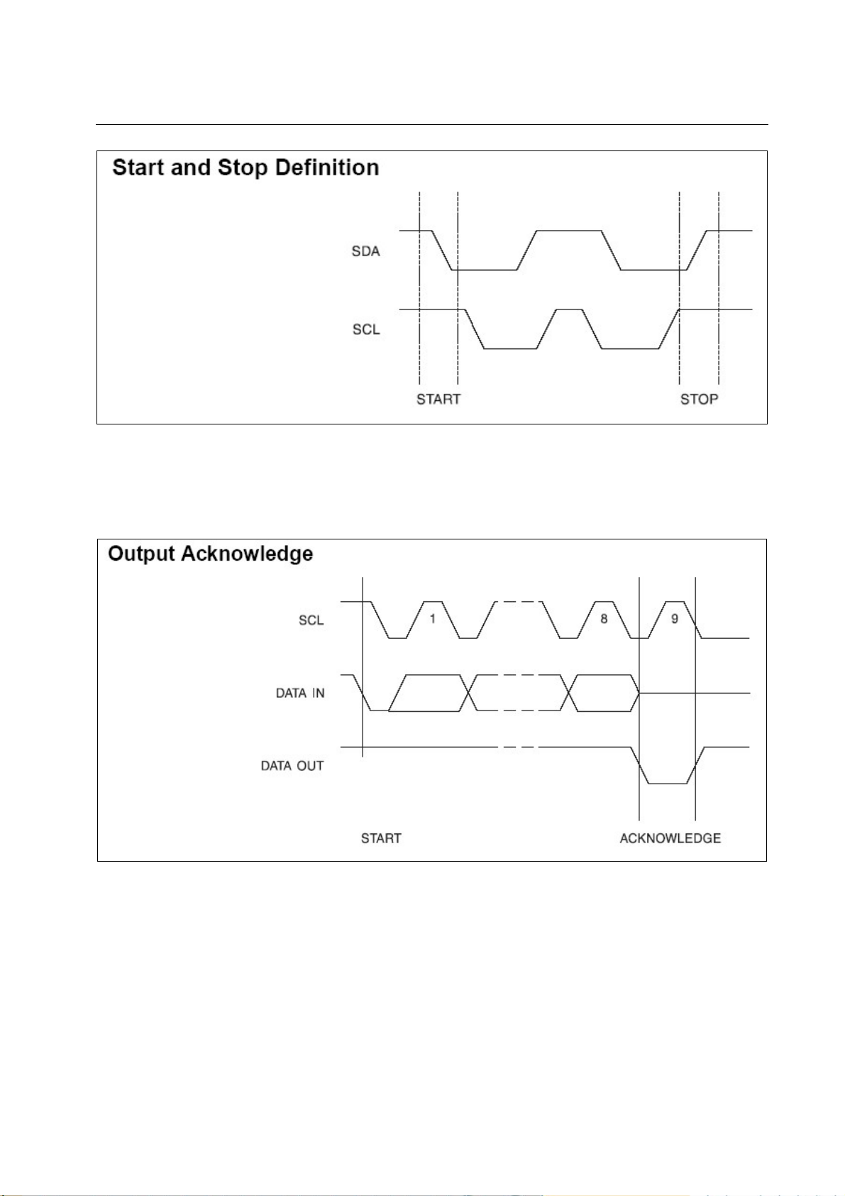
Start Condition: A high-to-low transition of SDA with SCL high is a start condition which must
precede any other command.
Stop Condition: A low-to-high transition of SDA with SCL high is a stop condition. After a read
sequence, the stop command will place the EEPROM in a standby power mode.
55
Page 56
SERVICE MANUAL TK-A/Q
Acknowledge:
All addresses and data words are serially transmitted to and from the EEPROM in 8
bit words. The EEPROM sends a zero to acknowledge that it has received each word. This happens
during the ninth clock cycle.
Standby Mode: The AT24C16A features a low power standby mode which is enabled: (a) upon
power-up and (b) after the receipt of the STOP bit and the completion of any internal operations.
Memory Reset: After an interruption in protocol, power loss or system reset, any 2-wire part can be
reset by following these steps: (a) Clock up to 9 cycles, (b) look for SDA high in each cycle while
SCL is high and then (c) create a start condition as SDA is high.
56
Page 57
SERVICE MANUAL TK-A/Q
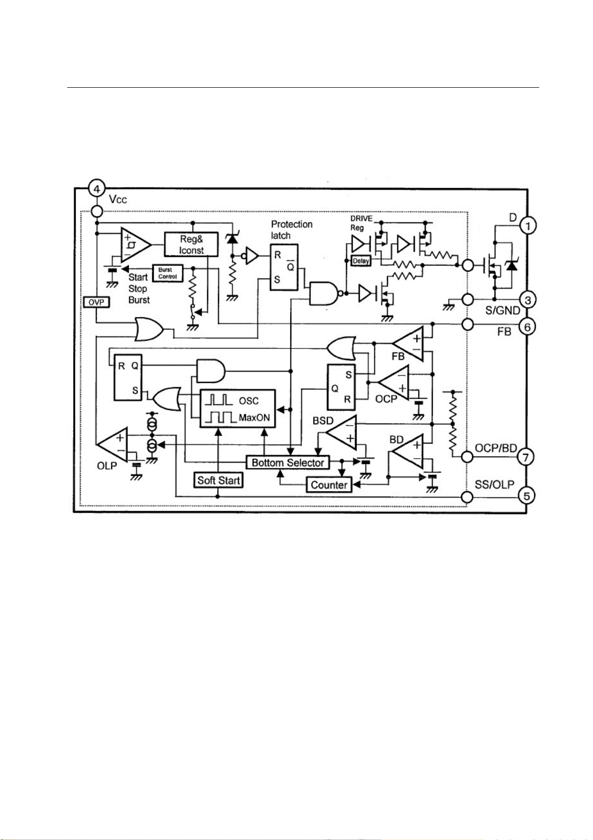
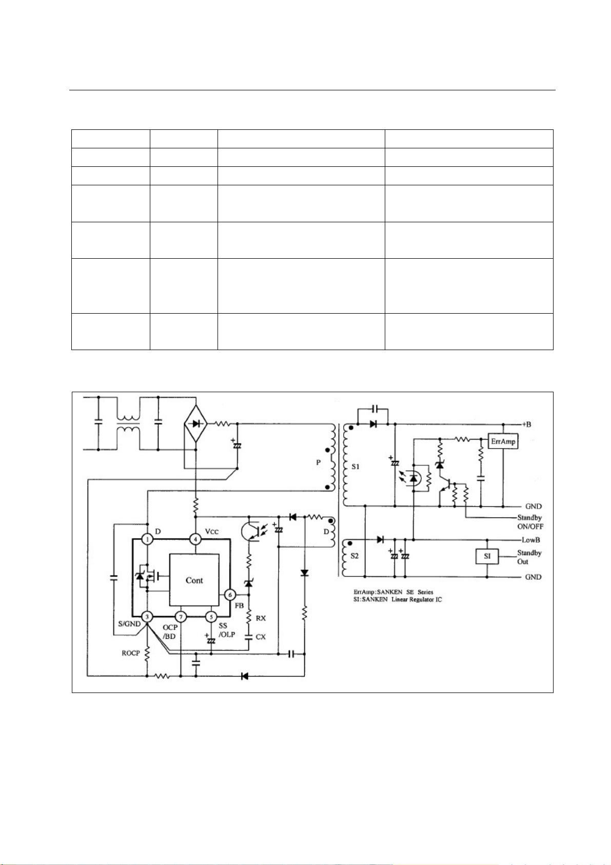
3. SWITCH POWER IC (N901)
3.1 STR-W6753
3.1.1 Block Diagram
57
Page 58
SERVICE MANUAL TK-A/Q
3.1.2 Functions of each terminal
Terminal No. Symbols Descriptions Functions
1 D Drain terminal MOSFET drain
3 S/GND Source/Ground terminal MOSFET Source/Ground
4 Vcc Power supply terminal Input of power supply for control
circuit
5 SS/OLP Delay at Overload/Soft Start set up
6 FB Feedback terminal Constant Voltage Control Signal
7 OCP/BD Overcurrent Protection Input/Bottom
3.1.3 Example Application Circuit
Ter minal
Detection Terminal
Overload Protection and Soft Start
Operation Time set up
Input, Burst(intermittent)mode
Oscillation Control
Overcurrent Detection Signal
Input/Bottom Detection Signal Input
58
Page 59
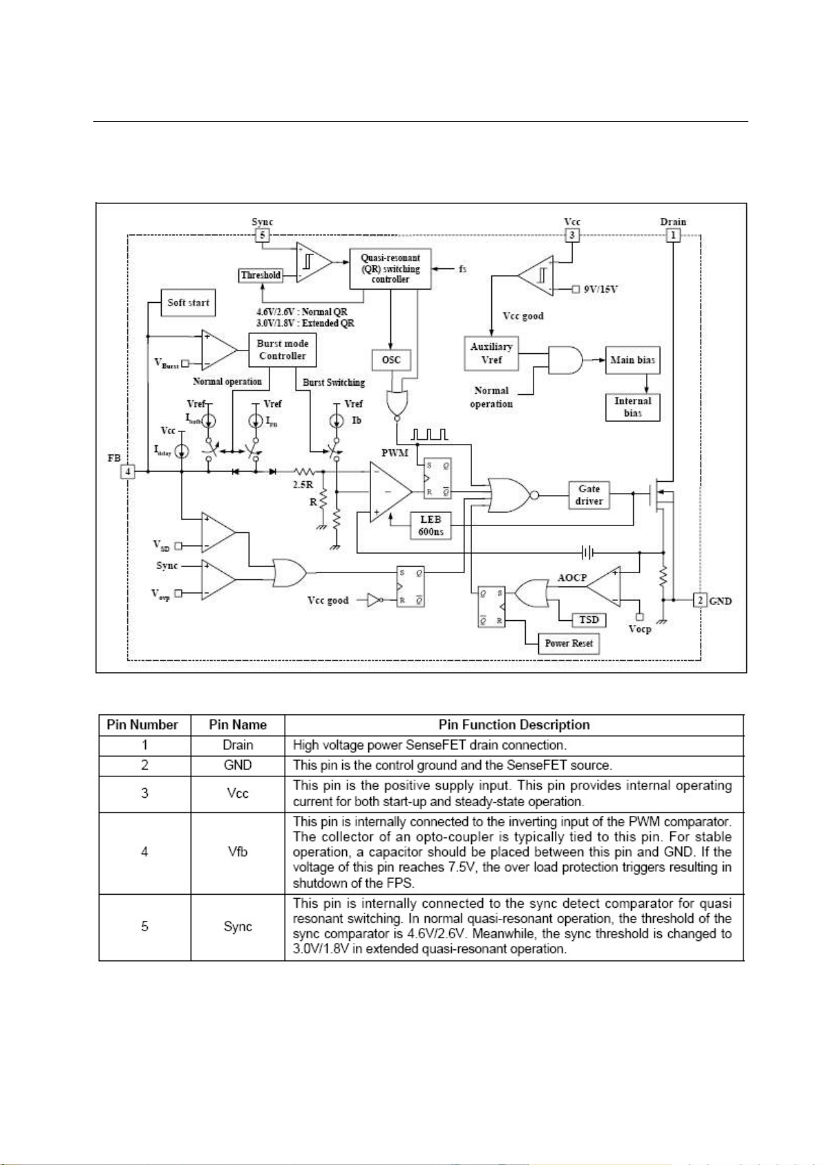
3.2 FSCQ1265RT
3.2.1 Internal Block Diagram
SERVICE MANUAL TK-A/Q
3.2.2 Pin Definitions
59
Page 60
SERVICE MANUAL TK-A/Q
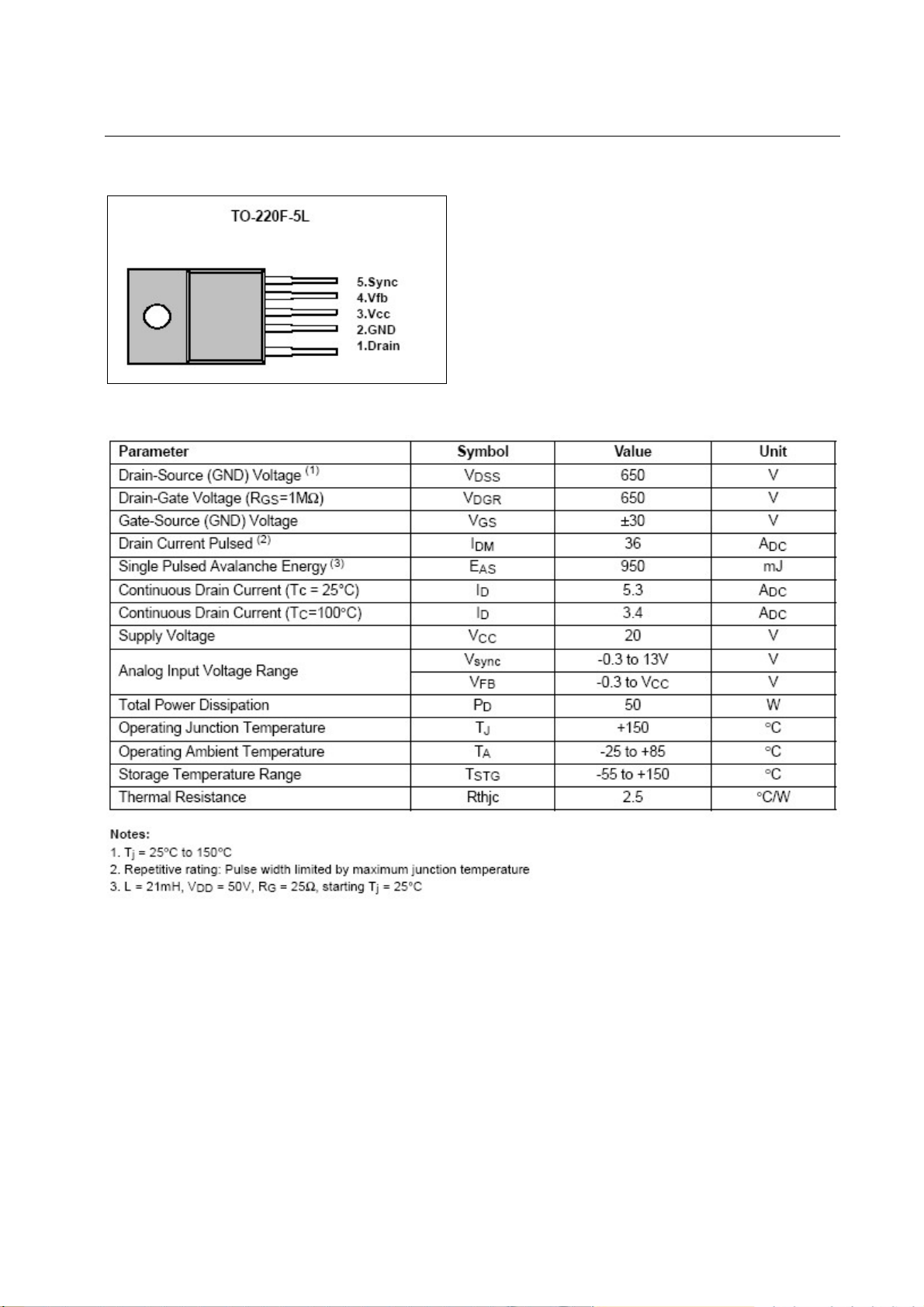
3.2.3 Pin Configuration
3.2.4 Absolute Maximum Ratings
60
Page 61
SERVICE MANUAL TK-A/Q
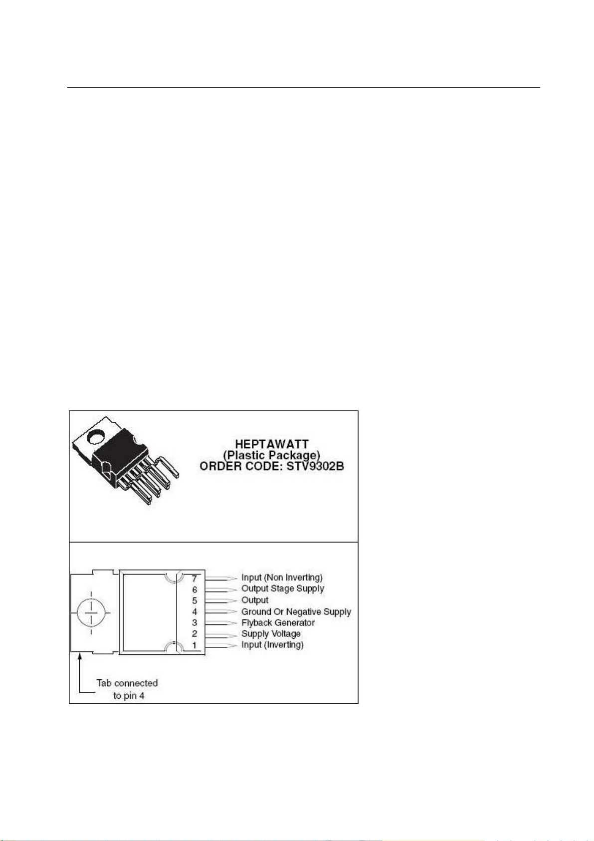
4. VERTICAL DEFLECTION BOOSTER (N401)
4.1 STV9302B
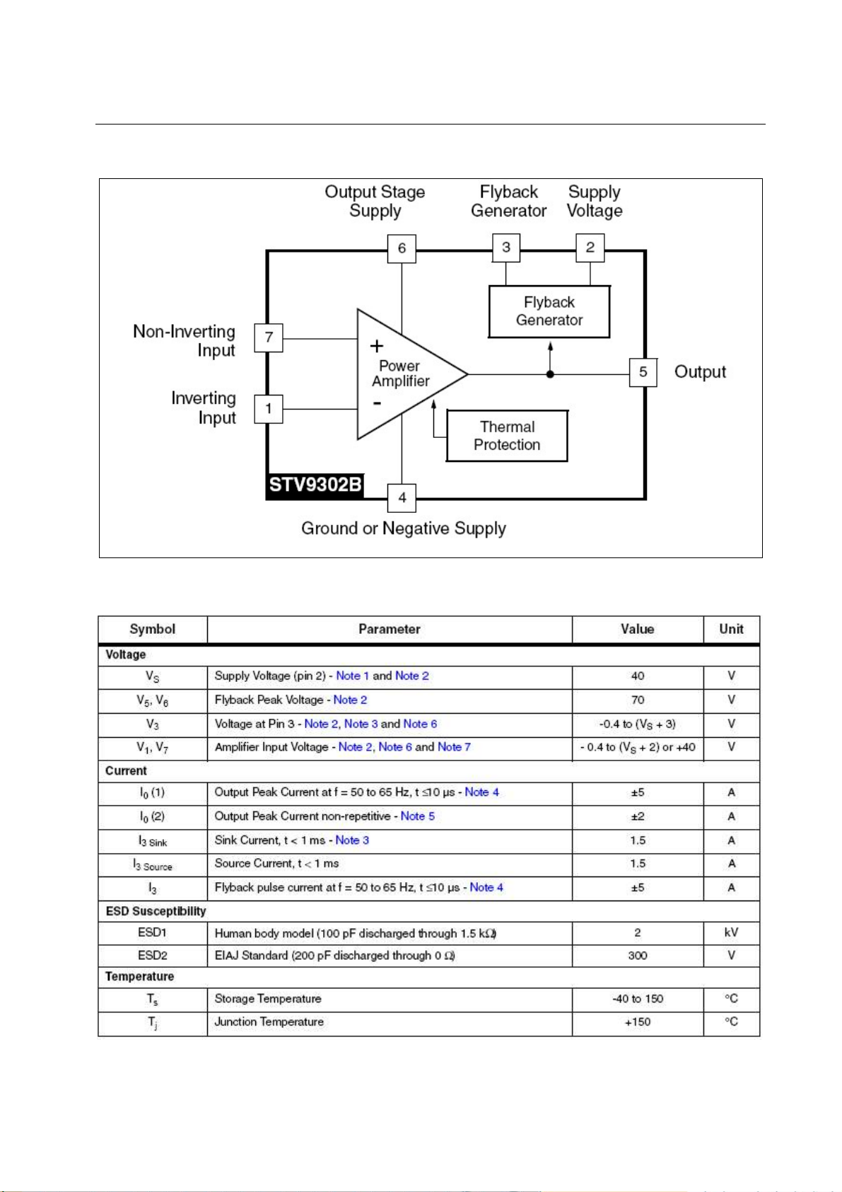
4.1.1 Main Features
■ Power Amplifier
■ Flyback Generator
■ Output Current up to 2 App
■ Thermal Protection
4.1.2 Description
The STV9302B is a vertical deflection booster designed for TV (50-60 Hz) applications.
This device, supplied with up to 35 V, provides up to 2 App output current to drive the vertical
deflection yoke.
The internal flyback generator delivers flyback voltages up to 70 V.
4.1.3 Pin Configuration
61
Page 62
4.1.4 Internal Block Diagram
SERVICE MANUAL TK-A/Q
4.1.5 Absolute Maximum Ratings
62
Page 63
SERVICE MANUAL TK-A/Q
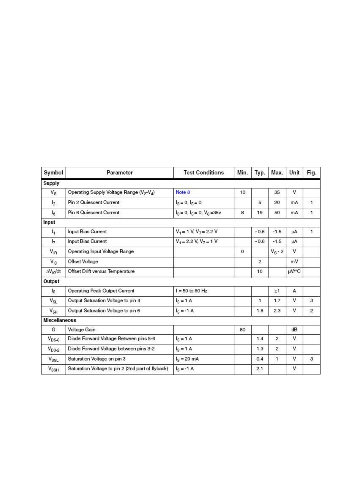
Note:1. Usually the flyback voltage is slightly more than 2 x VS. This must be taken into
consideration when setting VS.
2. Versus pin 4
3. V3 is higher than VS during the first half of the flyback pulse.
4. Such repetitive output peak currents are usually observed just before and after the flyback pulse.
5. This non-repetitive output peak current can be observed, for example, during the
Switch-On/Switch-Off phases. This peak current is acceptable providing the SOA is respected
(Figure 8 and Figure 9).
6. All pins have a reverse diode towards pin 4, these diodes should never be forward-biased.
7. Input voltages must not exceed the lower value of either VS + 2 or 40 volts.
4.1.6 Electrical Characteristics
8. In normal applications, the peak flyback voltage is slightly greater than 2 x (Vs – V4). Therefore,
(Vs - V4) = 35 V is not allowed without special circuitry.
63
Page 64
SERVICE MANUAL TK-A/Q
4.1.7 DC-coupled Application
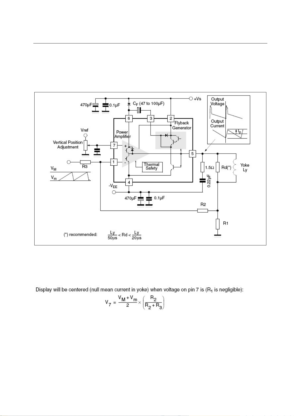
The yoke can be coupled either in AC or DC. IN our TV, it is DC-coupled application.
When DC coupled , the display vertical position can be adjusted with input bias. On the other
hand, 2 supply sources (VS and -VEE) are required.
For calculations, treat the IC as an op-amp, where the feedback loop maintains V1 = V7.
4.1.7.1 Centering
64
Page 65
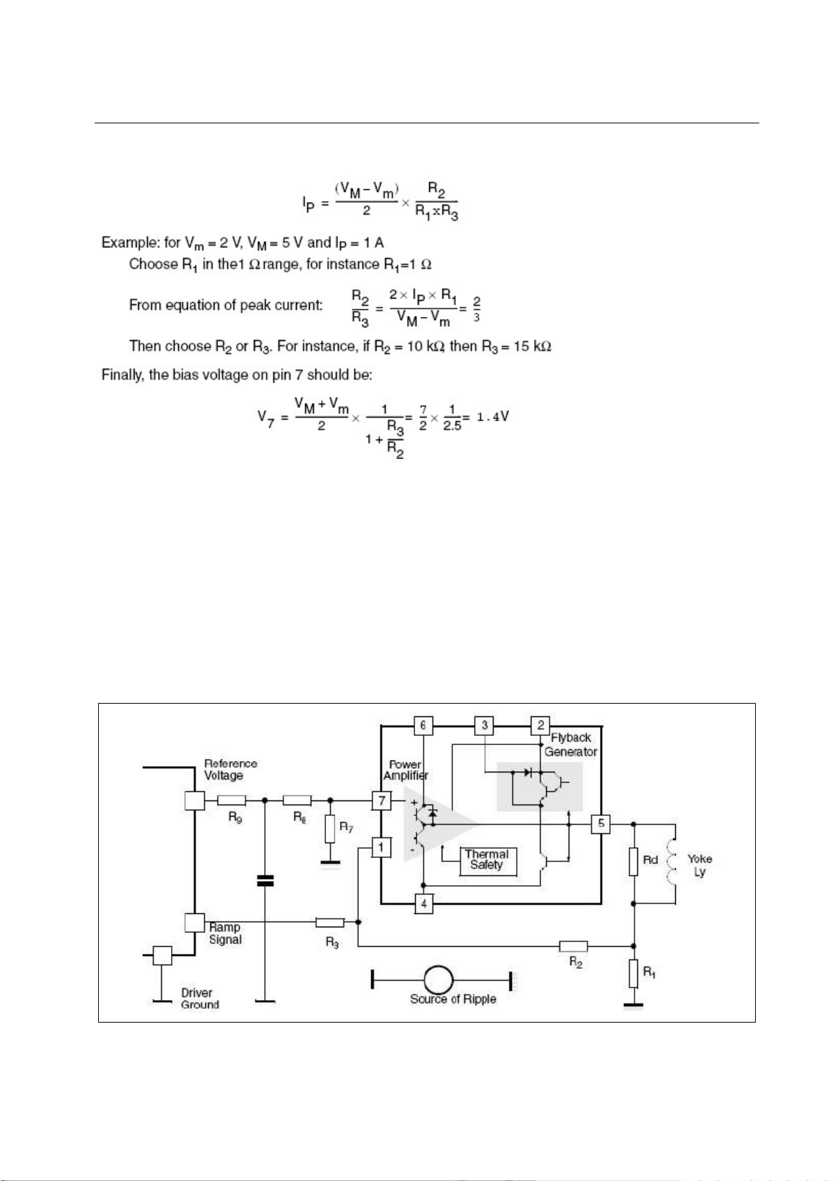
4.1.7.2 Peak Current
4.1.7.3 Ripple Rejection
SERVICE MANUAL TK-A/Q
When both ramp signal and bias are provided by the same driver IC, you can gain natural
rejection of any ripple caused by a voltage drop in the ground, if you manage to apply the same
fraction of ripple voltage to both booster inputs. For that purpose, arrange an intermediate point in
the bias resistor bridge, such that (R8 / R7) = (R3 / R2), and connect the bias filtering capacitor
between the intermediate point and the local driver ground. Of course, R7 should be connected to
the booster reference point, which is the ground side of R1.
65
Page 66
SERVICE MANUAL TK-A/Q
4.2 STV8172A and STV9325
STV8172A and STV9325 are the same as STV9302B, they are pin to pin compatible. They are
different from the output current only. STV9302B can output current up to 2Ap-p, STV9325 can
output current up to 2.5Ap-p, but STV8172A can output current up to 3Ap-p.
5. AUDIO POWER AMPLIFIER (N202)
5.1 TDA2614
TDA2614 is a 6W hi-fi audio power amplifier.
5.1.1 Features
· Requires very few external components
· No switch-on/switch-off clicks
· Input mute during switch-on and switch-off
· Low offset voltage between output and ground
· Hi-fi in accordance with IEC 268 and DIN 45500
· Short-circuit proof and thermal protected
· Mute possibility.
5.1.2 General Description
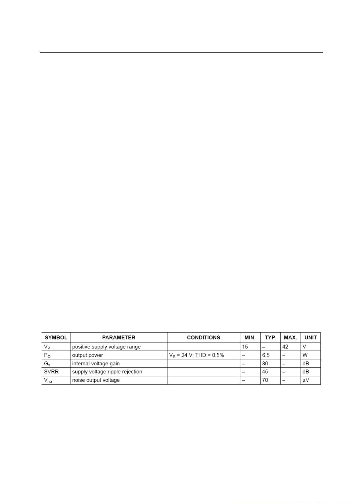
The TDA2614 is a power amplifier in a 9-lead single-in-line (SIL9) plastic medium power
package. It has been especially designed for mains fed applications, such as TV and radio.
5.1.3 Quick Reference Data
66
Page 67
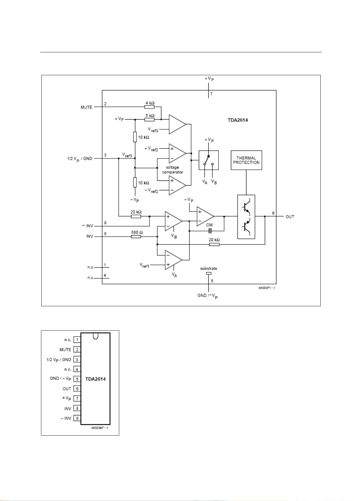
5.1.4 Block Diagram
SERVICE MANUAL TK-A/Q
5.1.5 Pin Configuration
67
Page 68
SERVICE MANUAL TK-A/Q
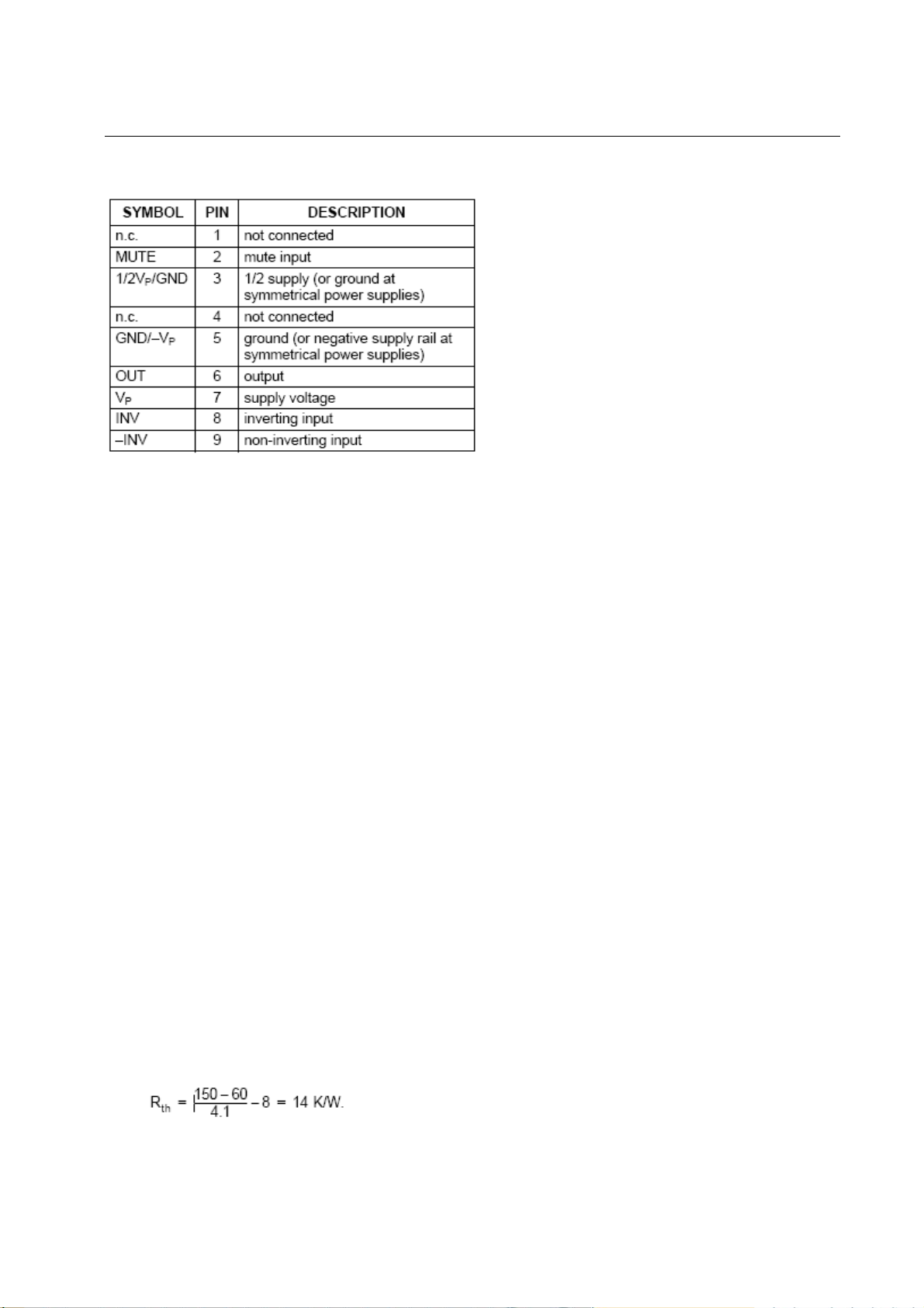
5.1.6 Pinning
5.1.7 Functional Description
The TDA2614 is a hi-fi power amplifier designed for mains fed applications, such as radio and
TV. The circuit is optimally designed for asymmetrical power supplies, but is also well-suited to
symmetrical power supply systems.
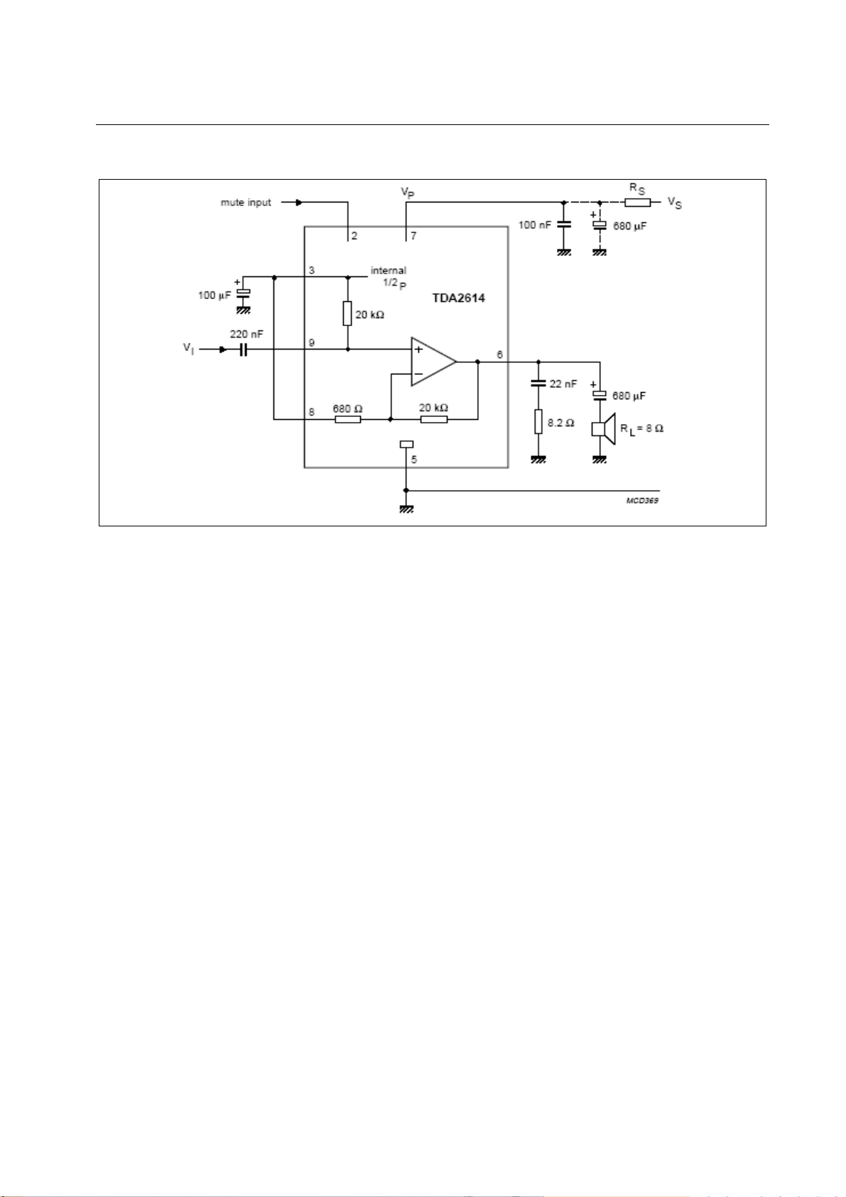
An output power of 6 W (THD = 0.5%) can be delivered into an 8Ωload with a supply of 24V.
The gain is internally fixed at 30 dB, thus offering a low gain spread.
A special feature is the input mute circuit. This circuit disconnects the non-inverting inputs
when the supply voltage drops below 10 V, while the amplifier still retains its DC operating
adjustment. The circuit features suppression of unwanted signals at the input, during switch-on and
switch-off.
The mute circuit can also be activated via pin 2. When a current at 300 µA is present at pin 2,
the circuit is in the mute condition.
The device is provided with two thermal protection circuits. One circuit measures the average
temperature of the crystal and the other measures the momentary temperature of the power
transistors. These control circuits attack at temperatures in excess of +150 ℃, so a crystal operating
temperature of max. +150 ℃ can be used without extra distortion.
With the derating value of 8 K/W, the heatsink can be calculated as follows:
at RL = 8Ω and VS = 24 V, dissipation is 4.1 W.
With a maximum ambient temperature of 60 ℃, the thermal resistance of the heatsink is:
68
Page 69
SERVICE MANUAL TK-A/Q
5.1.8 Test and application circuit with asymmetrical power supply
5.2 TDA2615
TDA2615 is a 2 X 6 W hi-fi audio power amplifier.
5.2.1 Features
· Requires very few external components
· No switch-on/switch-off clicks
· Input mute during switch-on and switch-off
· Low offset voltage between output and ground
· Excellent gain balance of both amplifiers
· Hi-fi in accordance with “IEC 268” and “DIN 45500”
· Short-circuit proof and thermal protected
· Mute possibility.
5.2.2 General Description
The TDA2615 is a dual power amplifier in a 9-lead plastic single-in-line (SIL9MPF) medium
power package. It has been especially designed for mains fed applications, such as stereo radio and
stereo TV.
69
Page 70
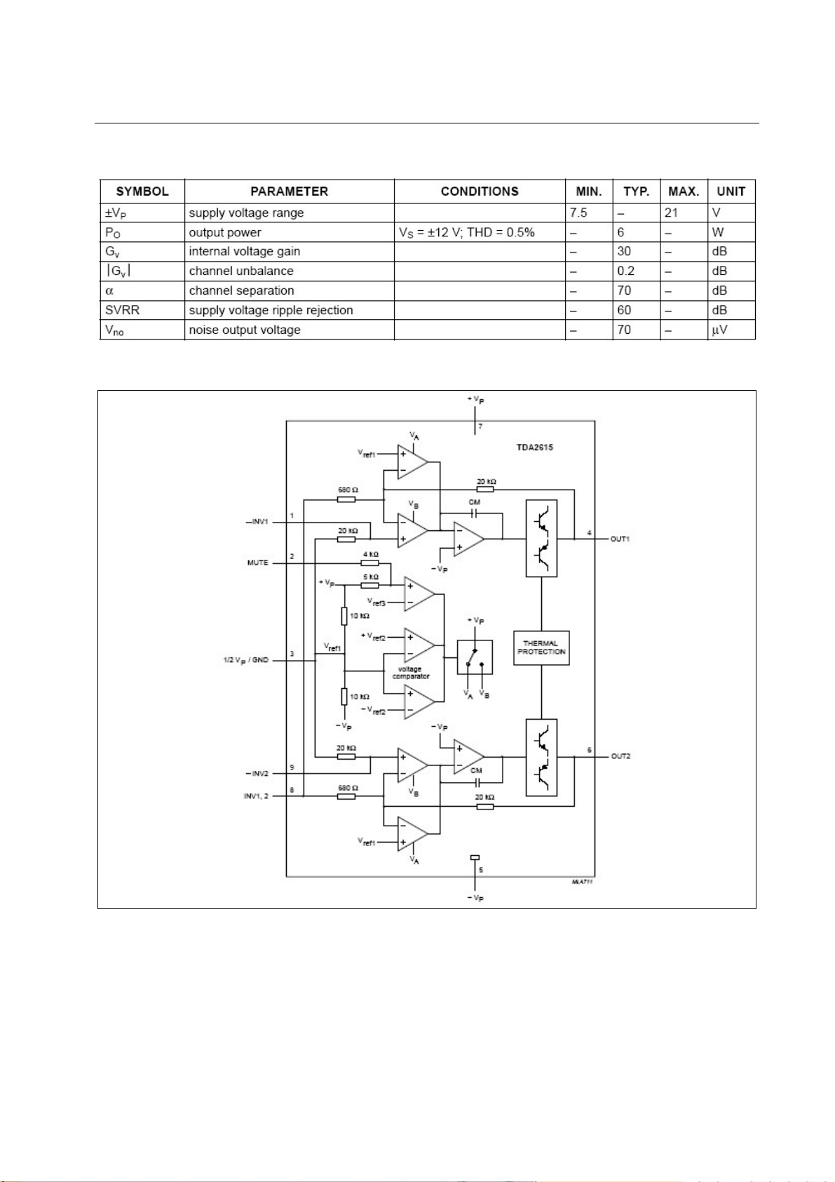
5.2.3 Quick Reference Data
5.2.4 Block Diagram
SERVICE MANUAL TK-A/Q
5.2.5 Functional Description
The TDA2615 is a hi-fi stereo amplifier designed for mains fed applications, such as stereo
radio and stereo TV. The circuit is optimally designed for symmetrical power supplies, but is also
well-suited to asymmetrical power supply systems.
70
Page 71
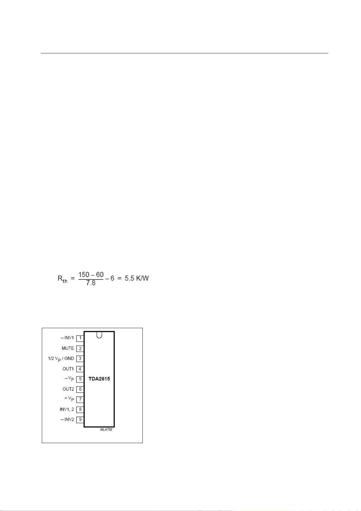
SERVICE MANUAL TK-A/Q
An output power of 2×6 W (THD = 0.5%) can be delivered into an 8Ωload with a
symmetrical power supply of ±12 V. The gain is internally fixed at 30 dB, thus offering a low gain
spread and a very good gain balance between the two amplifiers (0.2 dB).
A special feature is the input mute circuit. This circuit disconnects the non-inverting inputs
when the supply voltage drops below ±6 V, while the amplifier still retains its DC operating
adjustment. The circuit features suppression of unwanted signals at the inputs, during switch-on and
switch-off.
The mute circuit can also be activated via pin 2. When a current of 300 µA is present at pin 2,
the circuit is in the mute condition.
The device is provided with two thermal protection circuits. One circuit measures the average
temperature of the crystal and the other measures the momentary temperature of the power
transistors. These control circuits attack at temperatures in excess of +150 ℃, so a crystal operating
temperature of max. +150 ℃ can be used without extra distortion.
With the derating value of 6 K/W, the heatsink can be calculated as follows:
at RL = 8Ω and VS = ±12 V, the measured maximum dissipation is 7.8 W.
With a maximum ambient temperature of +60 °C, the thermal resistance of the heatsink is:
The metal tab has the same potential as pin 5.
5.2.6 Pin Configuration
71
Page 72
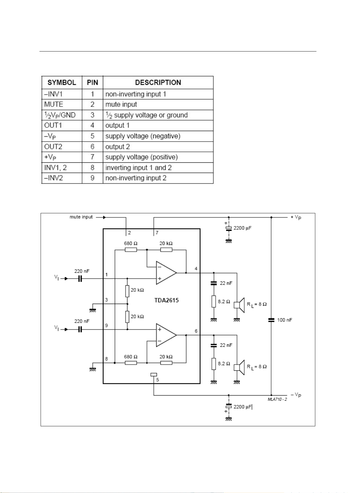
SERVICE MANUAL TK-A/Q
5.2.7 Pinning
5.2.8 Application circuit with symmetrical power supply
72
Page 73
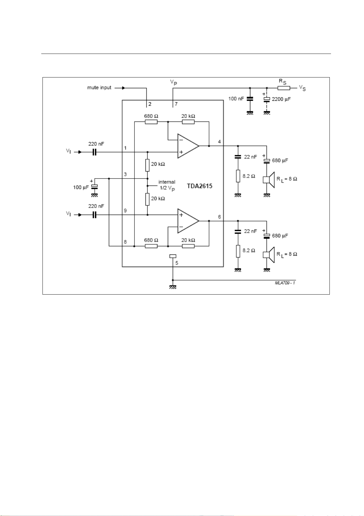
SERVICE MANUAL TK-A/Q
5.2.9 Application circuit with asymmetrical power supply
5.3 TDA2616(Q)
TDA2616(Q) is a 2 x 12 W hi-fi audio power amplifiers. The TDA2616 and TDA2616Q are
dual power amplifiers. The TDA2616 is supplied in a 9-lead single-in-line (SIL9) plastic power
package (SOT131), and is pin to pin compatible with TDA2615, while the TDA2616Q is supplied in
a 9-lead SIL-bent-to-DIL plastic power package (SOT157). They have been especially designed for
mains fed applications, such as stereo radio and stereo TV.
73
Page 74
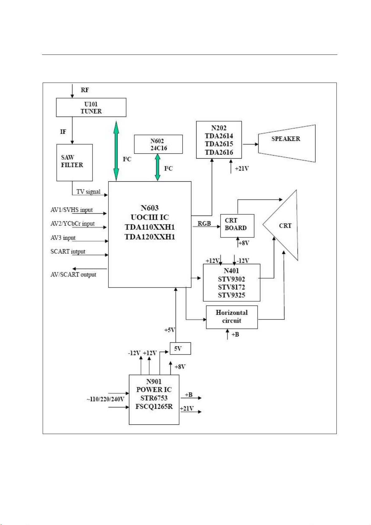
SERVICE MANUAL TK-A/Q
TV BLOCK DIAGRAM
74
Page 75
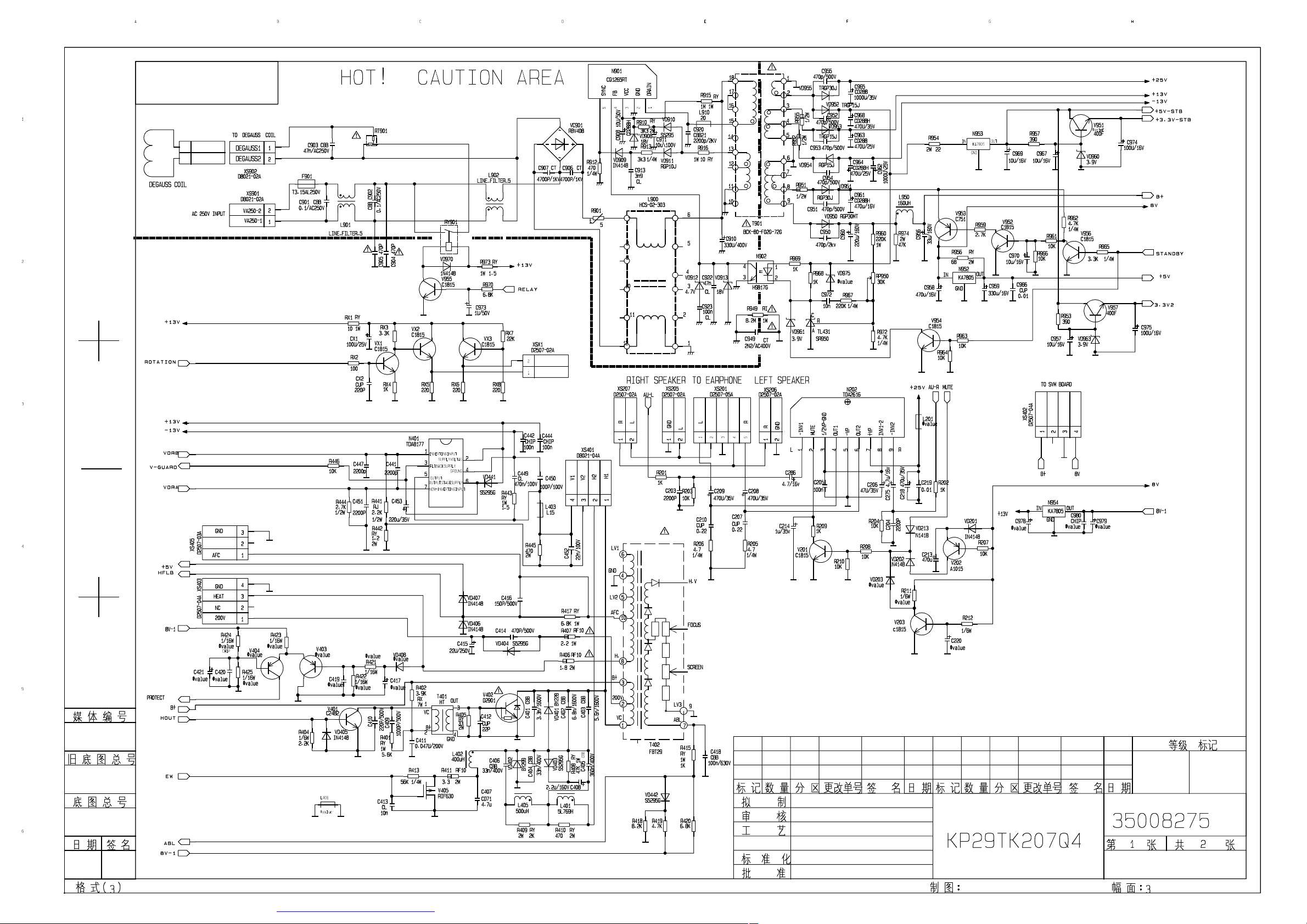
PDF 文件以 "PDF 制作工厂" 试用版创建 http://www.fineprint.com
Page 76
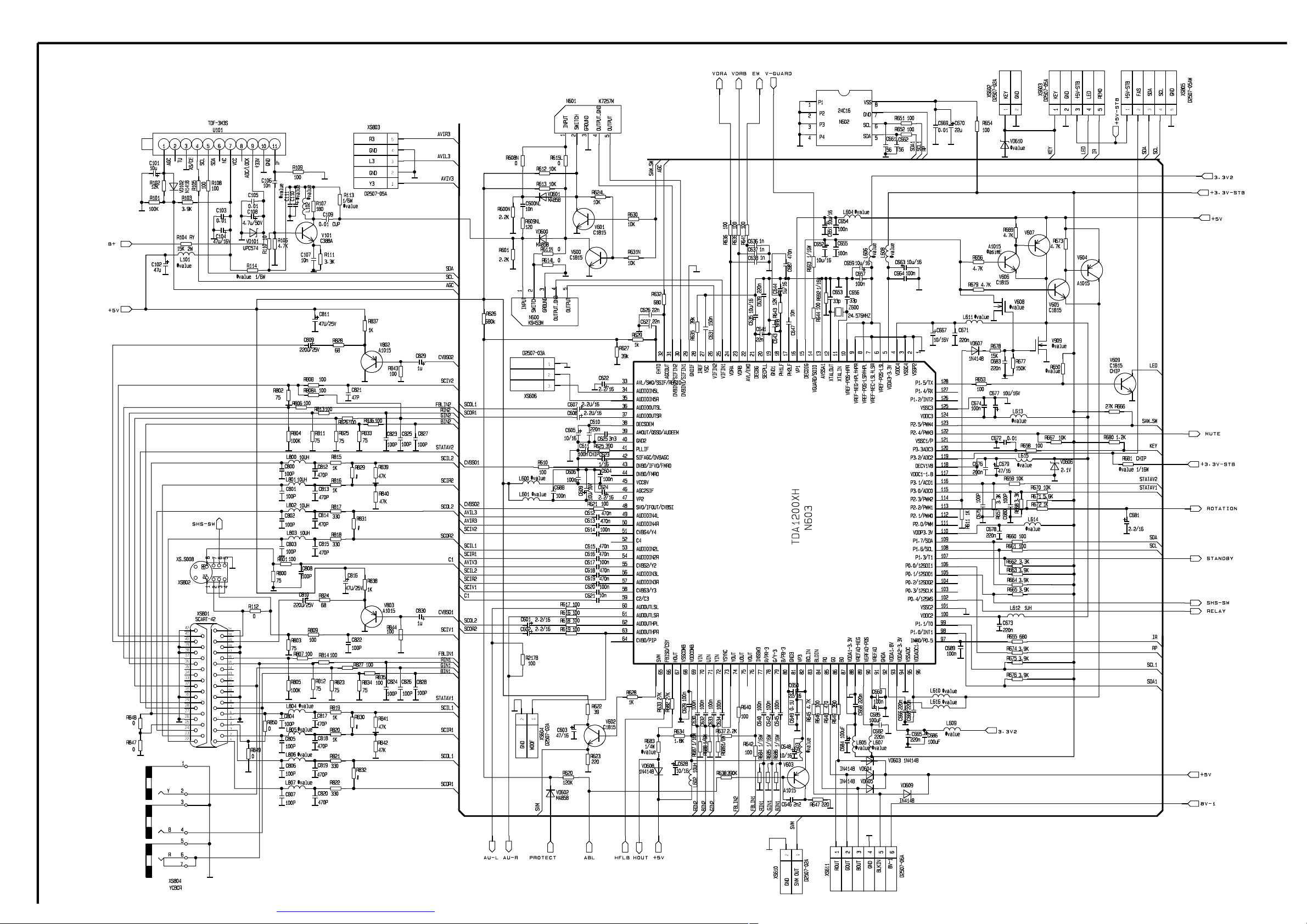
PDF 文件以 "PDF 制作工厂" 试用版创建 http://www.fineprint.com
Page 77
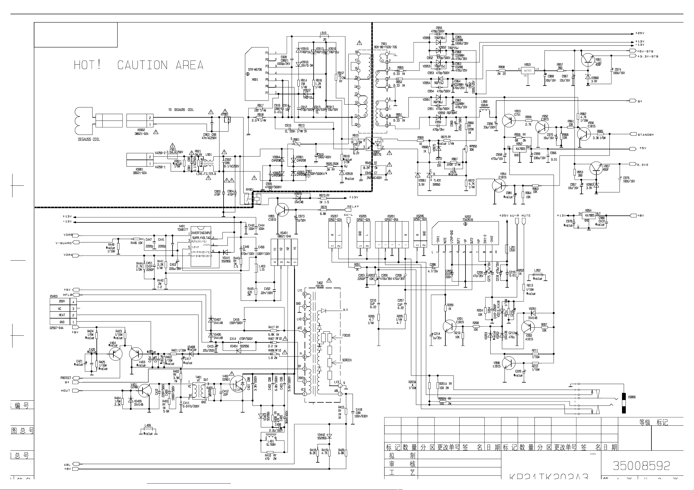
PDF 文件以 "PDF 制作工厂" 试用版创建 http://www.fineprint.com
Page 78
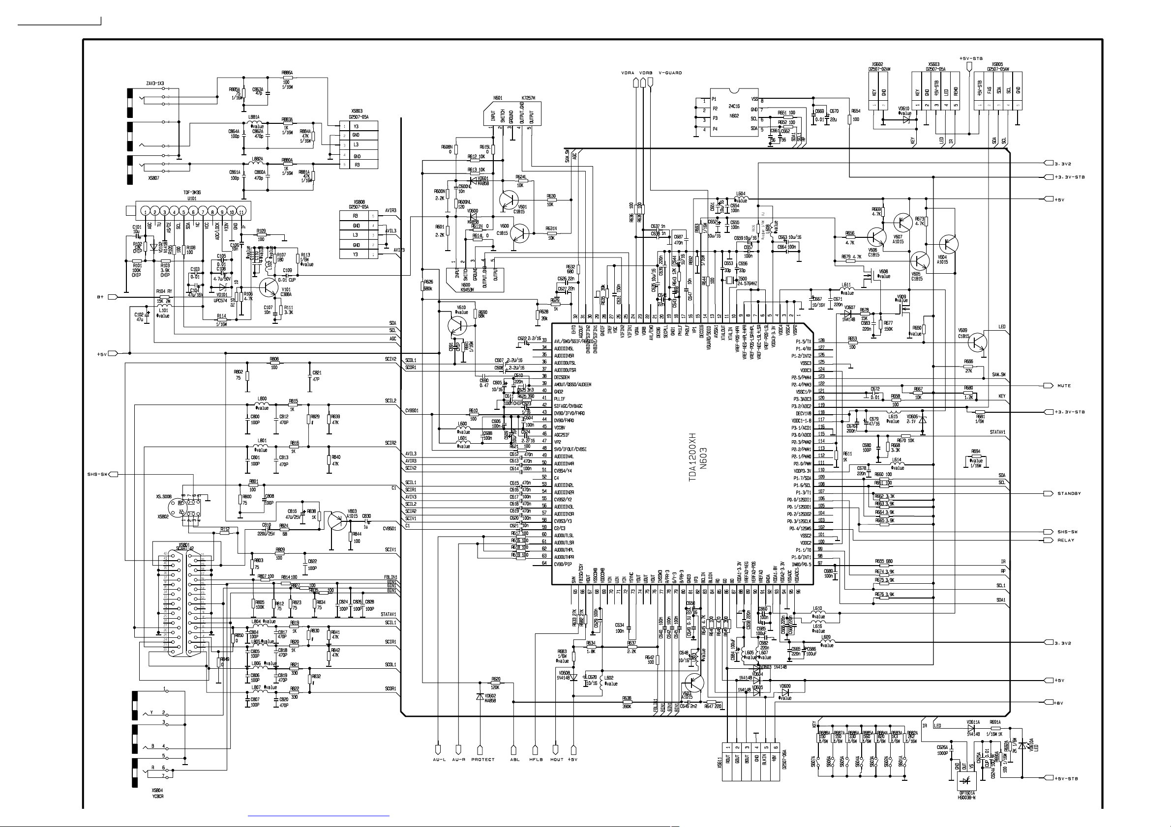
PDF 文件以 "PDF 制作工厂" 试用版创建 http://www.fineprint.com
 Loading...