

KLA RFSC812A, RFWC812A Users Manual

Non-Contact Integral Wafer™
User Manual
5451 Patrick Henry Dr.
Santa Clara, CA 95054
408-986-5600
Fax 408-986-5601
info@sensarray.com
www.sensarray.com

Copyright © 2006 by °SensArray® Corporation. All rights reserved.
UM-INT- 2007.04
SensArray reserves the right to modify, change, or improve any or
all specifications published in this document without notice.

Important Notices
Warranty
Integral Wafer System Hardware
SensArray Corporation warrants that the contact style or non-contact style Integral Wafer
Systems (“Products”) sold will be free from defects in material and workmanship, and
perform to SensArray’s applicable published specifications for a period of 12 months after
shipment for the Docking Station. The Integral Wafer is warranted for 6 months or a
specified number of operating hours, whichever occurs first. Refer to the specification
provided with your wafer for the exact warranty terms. The Products that comprise the
System shall include the Docking Station. The liability of SensArray hereunder shall be
limited to replacing or repairing, at its option, any defective Products that are returned
F.O.B. to SensArray’s plant in Santa Clara, CA. In no case are Products to be returned
without the purchaser first obtaining SensArray’s permission and Returned Materials
Authorization [RMA] number. In no event shall SensArray be liable for any consequential
or incidental damages. Products that have been subject to abuse, misuse, accident,
alteration, neglect, or unauthorized repair or installation are not covered by this warranty.
SensArray will make the final determination as to the existence and cause of any alleged
defect. SensArray is not responsible for maintaining or supplying any consumable
materials used in conjunction with this hardware. No warranty is made with respect to
any customized equipment or Products supplied with Integral Wafer systems where
produced to Purchaser’s specifications except as specifically stated in writing by
SensArray in the contract for such Products. The purchaser will pay the shipping costs of
returned materials to SensArray; SensArray will pay the cost of shipping
repaired/replaced material to Purchaser. This Warranty is the only warranty made by
SensArray with respect to the Product delivered hereunder and may be modified only by
a written instrument that is signed by a duly authorized officer of SensArray and accepted
by Purchaser. Except as provided above, SensArray makes no warrantees, expressed or
implied, including any warranty of merchantability for a particular purpose.
Integral Wafer Software
SensArray Corporation warrants that (a) Integral Wafer software (Software) will perform
substantially in accordance with the accompanying written materials for a period of 12
months after shipment, and (b) the medium on which the Software is recorded will be free
from defects in materials and workmanship under normal use and service for a period of
12 months after shipment.
Faults caused by unauthorized modification, misuse or abuse of products, or problems
due to software not supplied by SensArray, are not covered by this Warranty. During the
Warranty Period, the purchaser may return failed Software to SensArray for repair or
replacement, at SensArray’s option. SensArray does not warrant that the operation of the
Software shall be uninterrupted or error free. The purchaser will first notify SensArray of
the nature of the problem and obtain a Returned Materials Authorization [RMA] number.
The purchaser will pay the costs of shipping returned Software to SensArray; SensArray
will pay the cost of shipping repaired/replaced Software to the purchaser. No other
warranty is expressed or implied. SensArray specifically disclaims the implied warranty
of merchantability and fitness for a specific application.
The Integral Wafer Software Documentation Materials (“Documentation”) are subject to
revision and change without notice. SensArray agrees to make a best effort attempt to
keep the purchaser advised of changes to the Documentation.

Software License Agreement
The Software is owned by SensArray Corporation and is protected by United States
copyright laws and international treaty provisions. Therefore, you must treat the Software
like any other copyrighted material. Under the Copyright Laws, the Integral Wafer
Software, or accompanying written materials, may not be copied, photo-copied,
reproduced, translated, in whole or in part, without the prior written permission of
SensArray.
You may make one copy of the Software solely for backup or archival purposes.
You may make 10 copies of the written materials accompanying the SensArray
Corporation-produced Software provided that such copies are solely for use by personnel
using the Integral Wafer System.
All rights not expressly granted to you in this Agreement are reserved to SensArray
Corporation.
Third-Party Software
Licenses for any software which was provided but not produced by SensArray
Corporation are granted solely and only by the original supplier or manufacturer and
solely and only with the supplier’s limitations and rights. Copying restrictions for such
software are governed solely and only by the original supplier or manufacturer’s license
or any other supplier-approved agreements, as applicable.
Trademarks
°SensArray
SensArray Corporation.
®
, Thermal MAP, Integral Wafer™, and Process Probe® are trademarks of
Windows and Excel are trademarks or trade names of Microsoft Corporation.
Any other terms mentioned in this document that are known to be trademarks or service
marks have been appropriately capitalized. Use of a term in this document should not be
regarded as affecting the validity of any trademark or service mark.
Some of the technology used in this product is acquired under license from the
management and operating contractor of the Oak Ridge National Laboratory on behalf of
the U.S. Department of Energy.
Radio Frequency Interference Compliance
Applies to the Storage Cases and RF Carrier Station
NOTE: This equipment has been tested and found to comply with the limits for a Class A
digital device, pursuant to part 15 of the FCC Rules. These limits are designed to provide
reasonable protection against harmful interference when the equipment is operated in a
commercial environment. This equipment generates, uses, and can radiate radio
frequency energy and, if not installed and used in accordance with the instruction manual,
may cause harmful interference to radio communications. Operation of this
equipment in a residential area is likely to cause harmful interference in which case the
user will be required to correct the interference at his own expense.
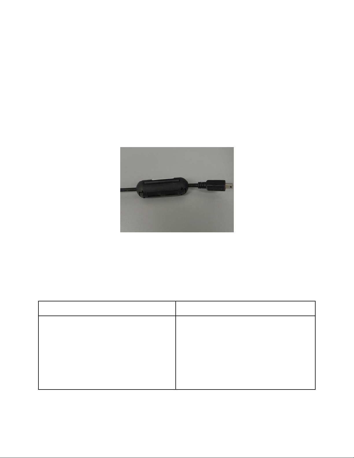
For the RF Carrier Station, only the USB cable supplied with the equipment is authorized
for use with this device; any other cable is not authorized and may cause undesired
interference, etc. Refer to Chapter 3 for product installation.
RF Carrier Station USB Cable
Product Modifications
Applies to the Storage Cases and RF Carrier Station
Changes or modifications to this equipment not expressly approved by KLA-Tencor may
void the user’s authority to operate the equipment.
English French
This device complies with Industry Canada
licence-exempt RSS standard(s). Operation is
subject to the following two conditions: (1) this
device may not cause interference, and (2) this
device must accept any interference, including
interference that may cause undesired operation of
the device.
Le présent appareil est conforme aux CNR
d'Industrie Canada applicables aux appareils radio
exempts de licence. L'exploitation est autorisée aux
deux conditions suivantes : (1) l'appareil ne doit pas
produire de brouillage, et (2) l'utilisateur de
l'appareil doit accepter tout brouillage
radioélectrique subi, même si le brouillage est
susceptible d'en compromettre le fonctionnement.

Table of Contents i
Using This Manual ..................................................................................................................iii
Overview.......................................................................................................................................... iii
What You Need to Know................................................................................................................. iii
Conventions Used in this Manual.....................................................................................................iv
Chapter 1 Overview..............................................................................................................1-1
The Integral Wafer System............................................................................................................ 1-1
Acquiring Data............................................................................................................................... 1-1
Analyzing Data .............................................................................................................................. 1-2
Chapter 2 System Setup .................................................................................................2-1
Before You Begin .......................................................................................................................... 2-1
Proper Wafer Handling Procedures........................................................................................... 2-1
Unpacking Your System................................................................................................................ 2-2
Removing the Wafer from the Storage Case............................................................................. 2-2
Charging the Equipment Before Use ........................................................................................ 2-4
Setting Up the Software................................................................................................................. 2-4
Preparing Equipment for the Cleanroom....................................................................................... 2-5
Cleaning the Equipment............................................................................................................ 2-5
Cleaning the Integral Wafer...................................................................................................... 2-5
Cleaning the Carrier Station...................................................................................................... 2-6
Chapter 3 Using the Charge and Communication Carrier Station .................................3-1
Using the Carrier Station................................................................................................................ 3-1
Removing the Wafer from the Carrier Station............................................................................... 3-6
Using the Wafer with the Carrier Station....................................................................................... 3-7
Chapter 4 Using the Integral Wafer System Controller Software ...................................4-1
Starting the Program ...................................................................................................................... 4-1
Wafer Time Limit Feature .............................................................................................................4-7
Defining a Survey .......................................................................................................................... 4-9
Transferring Wafer Data.............................................................................................................. 4-13
Appendix A Reference Information ................................................................................A-1
Sensor Bank Reference................................................................................................................. A-1
Correlating Sensor Coordinates.................................................................................................... A-2
Non-contact Integral Wafer User Manual

iii
UUssiinngg TThhiiss MMaannuuaall
Overview
This manual consists of the following sections.
• Chapter 1, Overview—Discusses features, components, and configurations of the
Non-contact Integral Wafer System.
• Chapter 2, System Setup—Discusses unpacking the system components, preparing
the equipment for the cleanroom, and connecting the system cables.
• Chapter 3, Using the Charge and Communication Carrier Station— provides an easy
means to prepare the wafer for data acquisition and to perform data retrieval.
• Chapter 4, Using the Integral Wafer Controller Software— Discusses acquisition
setup, acquisition features, and how to retrieve the measurement data using the
Carrier Stations.
• Appendix A, Reference Information- Wafer sensor location information.
What You Need to Know
This user manual assumes that you are familiar with the version of the Windows operating system
installed on your computer and can perform—as a minimum—the following tasks.
• Start (boot) the computer
• Log on to Windows
• Select from menus
• Select and open files
• Use a mouse or pointer, including how to point and click to select objects and
operate controls such as buttons
• Use standard window controls such as scroll bars
Non-contact Integral Wafer User Manual
iv Using This Manual
Conventions Used in this Manual
Several standard conventions are used in the text of this manual to make the information presented a
little clearer and easier to understand. Every attempt is made to be consistent in the application of
these conventions.
Note:
Bold
italic
Courier
Typeface
<Key>
»
Highlights important information.
Bold text indicates button names, icon names, and menu items.
Italic text indicates the section and/or chapter name in a cross-reference. For example:
See the Using the Acquisition Setup Window section of Chapter 3, Acquiring Data, for more
information. Italic text can also be used to emphasize a word or phrase.
Courier typeface indicates file names, directories, and text that you enter. For example:
The file is located in the C:\Sensarray\Configs directory.
A word offset by angle brackets indicates a key on the computer keyboard. For example:
After you specify the parameters, press the <Enter> key.
The twin arrow symbol indicates menu navigation. For example: Select
Acquisition»Acquire on the Thermal MAP Analysis window to open the Acquisition
Setup window. This tells you to click on Acquisition on the menu bar and then click on
the Acquire option from the drop-down menu.
Indicates important safety information. The icon is usually associated with a Warning or
Caution in the document describing potential for product damage or personal injury.
Other international standard icons specific to a particular hazard or action may be used
in place of the exclamation mark.
Non-contact Integral Wafer User Manual

1-1
Chapter 1 Overview
The Integral Wafer User Manual is designed to document the setup and use of the Integral
Wafer system in conjunction with the Integral Wafer Controller software. This manual will
discuss only the non-contact version of the Integral Wafer. The results of the measurement
run may be analyzed using the Thermal MAP Analysis Software included with the system.
The Thermal MAP Analysis software program is documented in the Thermal MAP Analysis
Software User Manual. A PDF version of this manual may be found in the C:\Sensarray\
Documents folder on your computer’s hard drive.
This chapter discusses the features of the non-contact Integral Wafer system.
The Integral Wafer System
The Integral Wafer has a complete measurement system embedded in the wafer to record
thermal surveys in semiconductor processing equipment without the need for wired
connections. Embedding the components within the wafer allows it to be treated like a
production wafer in most equipment, as long as it is within the operating temperature range
of the wafer.
The Integral Wafer system consists of an Integral Wafer, a carrier station for communicating
with and recharging the wafer, a USB cable, a laptop computer, and a CD containing the
software and drivers needed by the system.
The Integral Wafer system is delivered with a SensArray-provided laptop computer preloaded with all software. As an option, existing Thermal MAP laptop computer systems
may be upgraded to run the Integral Wafer software as long as you are running Windows
2000 or higher, and have an available USB port.
Integral Wafer systems are available in 200 mm and 300 mm versions, with different carrier
station options. The systems can acquire data from 1 to 64 analog channels, depending on
the model. The analog channels are divided into banks. Each bank is made up of up to 8
wafer sensors.
Measurements taken by the sensors are converted from analog to digital signals within the
onboard electronics.
Acquiring Data
Utilizing the Integral Wafer to acquire temperature data in your equipment is a simple
process. Measurement parameters, such as sensors to be used, scan rate, time delay, etc., are
set up using the Controller software. The wafer is then transferred to the measurement
chamber from a FOUP or cassette via robotic arms, and the thermal measurement survey
data is acquired. After the survey is complete, the wafer is returned to the Carrier station
and the data can be retrieved from the onboard memory. The data may then be analyzed
using Thermal MAP Analysis Software.
Non-contact Integral Wafer User Manual
1-2 Overview
Analyzing Data
The data files acquired by the Integral Wafer may be analyzed using Thermal MAP Analysis
Software to view XY graphs, contour maps, surface maps, animations, and data tables. For
more information on the use of the Analysis portion of the Thermal MAP 3 software, please
refer to the Thermal MAP 3 Analysis Software User Manual included on the CD.
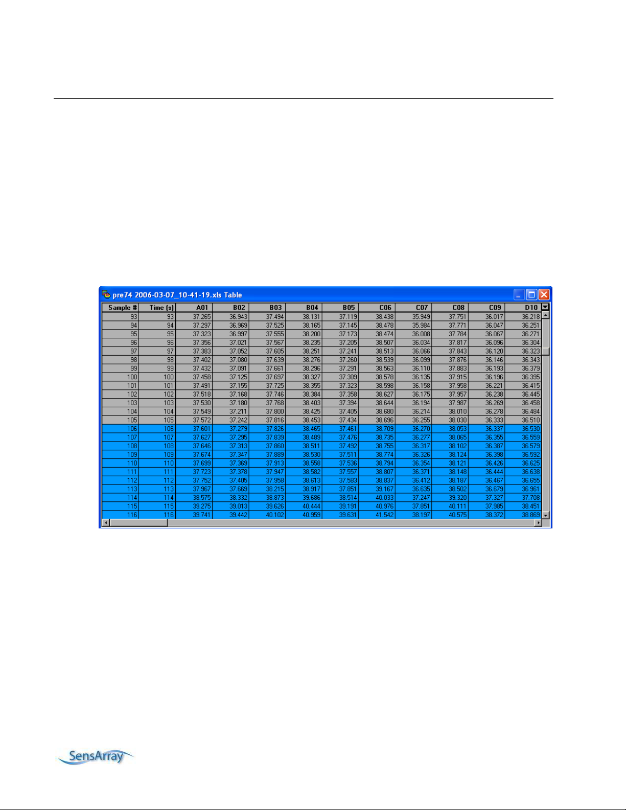
The data can be viewed and evaluated in table form if desired. A row in the table is called a
sample or a single-timed sampling of all of the sensors on the wafer. You use the sample
number to identify the table row of measurements collected at the sample time.
The first column in the table is the sample number. The second column is the time point at
which the sample was acquired. For example, as shown in Figure 1-1, sample 93 has a time
of 93 seconds. The remaining columns in the table are the temperatures of the sensors within
the wafer. Additional columns of data can be present if calculated values have been logged.
Figure 1-1. Sample Data Table from an Integral Wafer
During acquisition, Integral Wafer performs computations on acquired data, such as
determining the minimum, maximum, mean, range (max-min), and standard deviation of
all wafer sensor values for the sample, and logs the results in columns. These computed
values are referred to as calculated values.
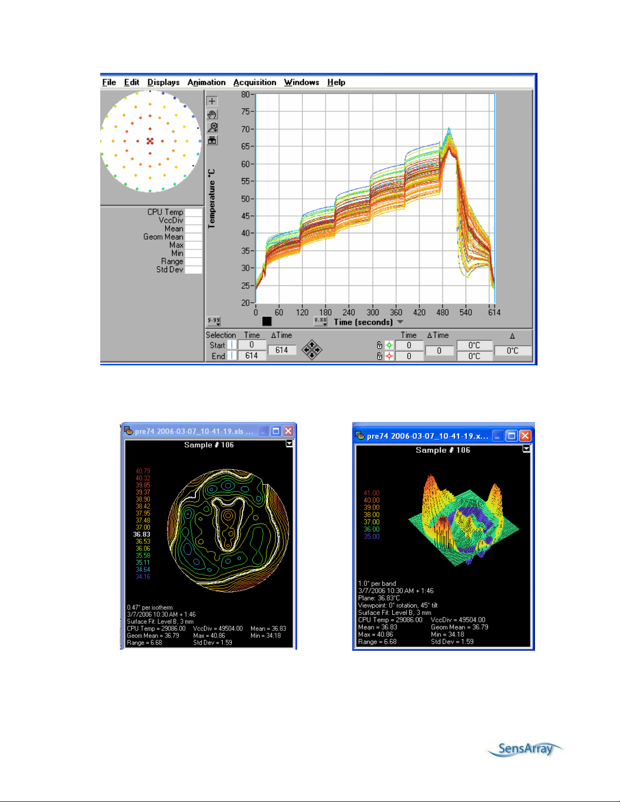
After acquiring, linearizing, and storing the sensor data, you can display or print the data as
a line plot graph, as shown in Figure 1-2. In addition, you can display data in a table or as a
wafer map.
Non-contact Integral Wafer User Manual
Overview 1-3
Figure 1-2. Displaying Data on a Line Plot Graph
You can also create a two-dimensional color contour map as shown in Figure 1-3 or a threedimensional surface map as shown in Figure 1-4 of a single sample point.
Figure 1-3. 2-Dimensional Color Contour Map Figure 1-4. 3-Dimensional Surface Map
Non-contact Integral Wafer User Manual

1-4 Overview
With the Animation feature, an animation of the survey data can be created. The animation
can be set for a particular range of the acquired samples, saved to a standard AVI file, and
replayed at any time. The AVI file can be sent to other computers not running the
Thermal MAP software and played using the Windows Media Player or other compatible
video players.
Data may also be exported to a spreadsheet program, edited in the spreadsheet, and loaded
back to Thermal MAP for further analysis.
Non-contact Integral Wafer User Manual

2-1
CChhaapptteerr 22 SSyysstteemm SSeettuupp
Before you can begin working with the non-contact Integral Wafer system, you need to unpack the
system components, prepare the equipment for transfer to the cleanroom, and charge the wafer
batteries.
Before You Begin
Before using the Integral Wafer, there are several safety and handling precautions that should be
noted. Please read the information provided in this manual and become familiar with the Integral
Wafer before attempting your first thermal survey.
• Operation of Integral Wafer outside of its specified temperature range could result in
unreliable readings and/or damaged wafers. Please review the recommended
operating range for your particular model of Integral Wafer.
• Rotational speeds up to 5000 rpm have been tested and found to be safe. While it is
possible that even higher rotational speed might be reached without damage to the
wafer or spin plate, SensArray cannot provide any guarantees above 5000 rpm.
Proper Wafer Handling Procedures.
While the Integral Wafer is designed to survive in a semiconductor fabrication environment,
reasonable care must be taken to prevent damage to the components on the wafer, or breaking the
wafer.
• Always wear gloves whenever you handle the wafer.
• Hold the wafer by the edges only or support from the backside of the wafer with
your hand or with a vacuum wand. In some situations, you may have to grasp the
edge of the wafer with your gloved fingers to prevent dropping the wafer, as when
you try to insert the wafer into your equipment or a carrier station.
• Never place the wafer on an uneven surface. A small downward pressure on the
wafer applied at the right point could cause the wafer to break or cause cracks
within the silicon.
Non-contact Integral Wafer User Manual
2-2 System Setup
Unpacking Your System
Inventory all items and compare to the packing list included with the shipment.
Retain all packaging materials for the system. This is required for the return of the
Integral Wafer for repairs or recalibration.
If any parts are missing or damaged, contact SensArray immediately. Be prepared to provide a list
of the missing and/or damaged components, the Purchase Order Number, and the SensArray Sales
Order Number.
NOTE: Do not return components without contacting SensArray first and obtaining a Return Material
Authorization. When returning components to SensArray, you must repack the equipment in the original
packing material. Failure to properly pack the components may result in additional damage to the equipment.
Removing the Wafer from the Storage Case
The non contact Integral Wafer storage case is designed to keep the Integral Wafer batteries
charged to the optimum level for an extended period of 1 to 2 years. This is done by periodically
checking the status of the batteries and recharging the batteries when their voltage drops below a
threshold.
CAUTION: The storage case is not designed to be used to recharge wafers after acquiring
data. The storage case may not be used as a carrier station. It is used only to store a wafer
when the wafer is not in use.
The wafer will be maintained in the storage case until it is needed. To use the wafer, place the
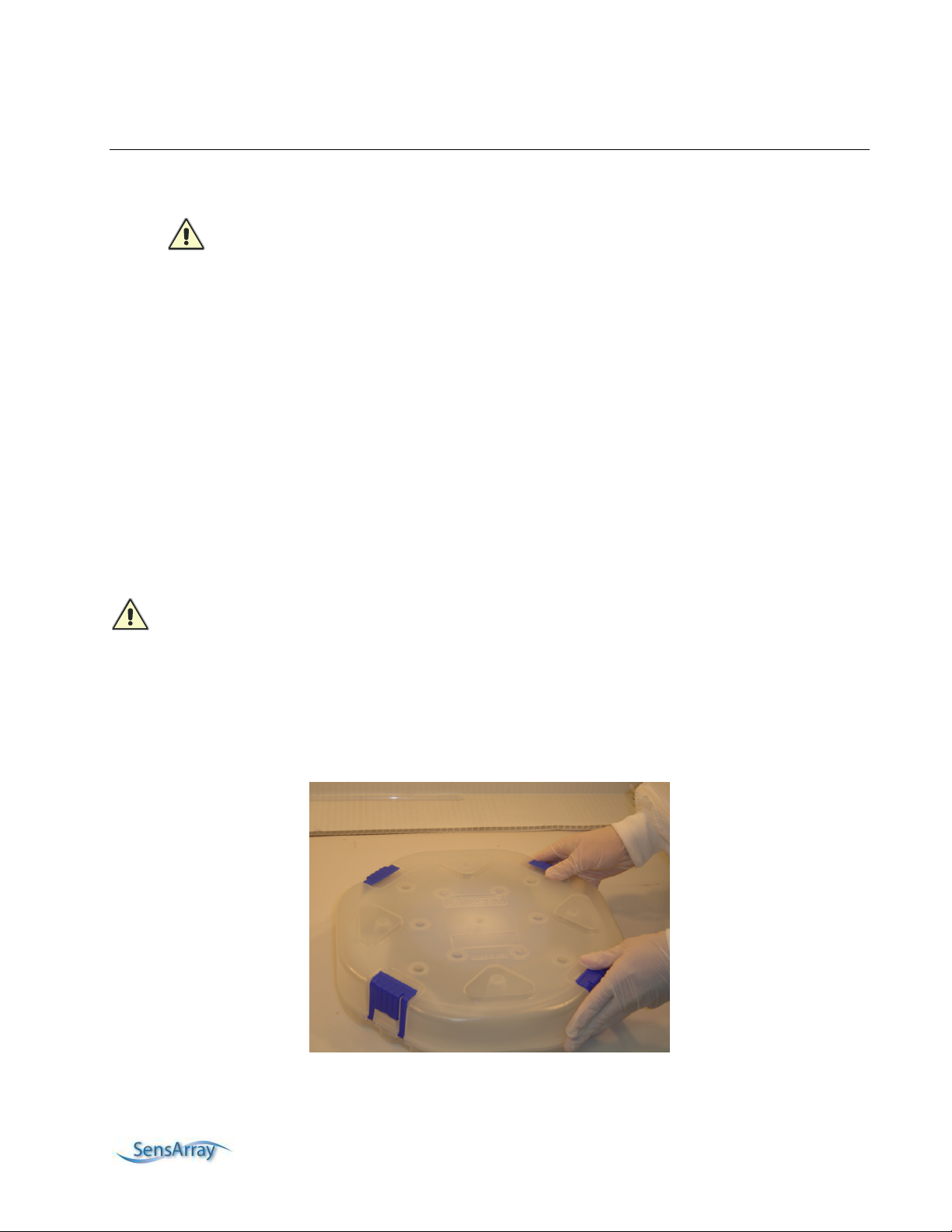
horizontal wafer shipper case right side up on a clean work surface and open the latches on the
case, as shown in Figure 2-1. Remove the lid. Locate the Charge and Communication (C/C) Carrier
Station near the storage case.
Figure 2-1. Opening the 300mm storage case
Non-contact Integral Wafer User Manual
System Setup 2-3
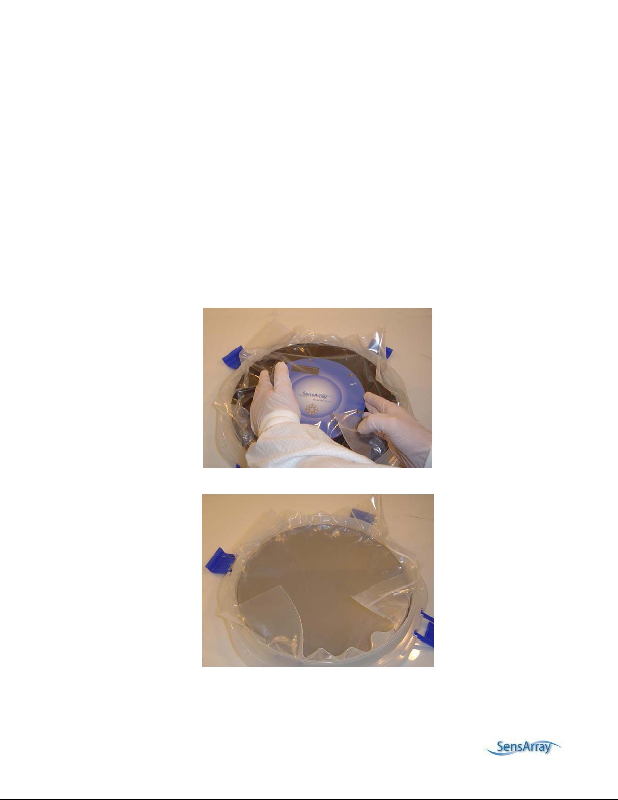
The maintenance module is placed on top of the wafer to allow for wireless maintenance. The
module is enclosed and sealed in a clean room compatible plastic bag. Do not remove the
maintenance module from its bag. It is there to ensure that the surface the wafer comes into contact
with is clean.
There is an LCD screen that indicates the wafer serial number and battery voltage. A blinking blue
LED also indicates that the wafer is good. If the wafer is not viable, the screen will indicate ‘no
wafer present’. The maintenance module must be reset to force it to search for a wafer by pressing
the reset button. The module will then spend approximately 15 seconds looking for a wafer in its
presence. If a wafer is present (centered and against the coil) and the module is unable to detect the
wafer, try to place the wafer in the carrier station to check the wafer state. If wafer looks healthy in
the carrier, the storage case may be problematic. Contact SensArray technical support for help.
To remove the wafer from the storage case, remove the aluminum liner from the case to expose the
maintenance module. Lift the maintenance module out of the case and place it in a clear area on the
work surface. Carefully remove the wafer from the case and place it in the C/C carrier station.
Figure 2-2. Lifting maintenance module
Figure 2-3. Remove wafer from case
Non-contact Integral Wafer User Manual
 Loading...