

Page 1

CREATE YOUR OWN SPEAKER DOCK WITH THIS
ESSENTIAL INFORMATION
BUILD INSTRUCTIONS
CHECKING YOUR PCB & FAULT-
FINDING
MECHANICAL DETAILS
WORKS
STEREO AMPLIFIER KIT
HOW THE KIT
Version 2.0
Page 2
Stereo Amplifier Essentials
PCB Ref
Value
Colour Bands
R1 & R2
10K
Brown, black, orange
R3 & R4
4.7Yellow, purple, gold
R5 & R6
100K
Brown, black, yellow
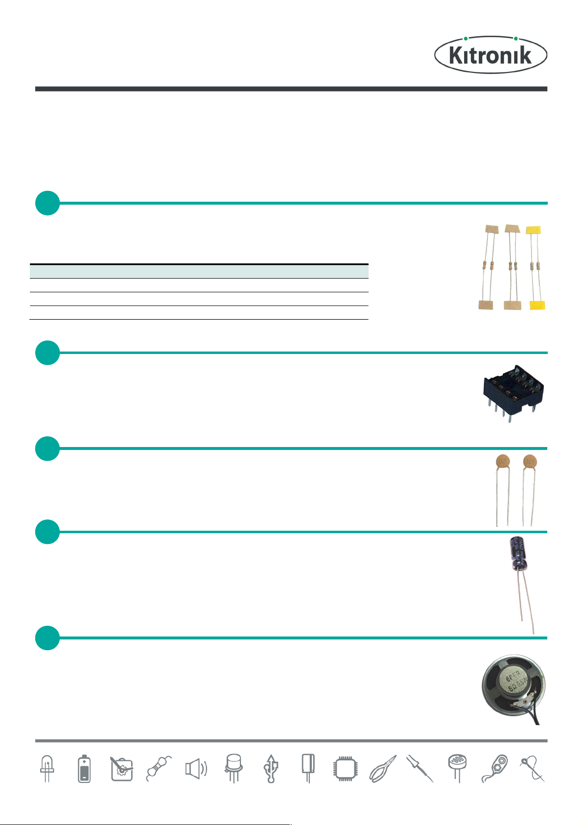
PLACE RESISTORS
1
SOLDER THE IC HOLDER
2
SOLDER THE
CERAMIC DISC CAPACITORS
3
SOLDER THE ELECTROLYTIC CAPACITORS
4
CONNECT THE
SPEAKERS
5
www.kitronik.co.uk/2136
Build Instructions
Before you start, take a look at the Printed Circuit Board (PCB). The components go in the side with the writing on
and the solder goes on the side with the tracks and silver pads.
Start with the six resistors:
The text on the PCB shows where R1, R2 etc go.
Ensure that you put the resistors in the right place.
Solder the Integrated Circuit (IC) holder in to IC1. When putting this into the board, be sure to get it
the right way around. The notch on the IC holder should line up with the notch on the lines marked
on the PCB. Once this has been done insert the 8 pin IC into this socket, making sure that the notch
on the device matches the notch on the IC holder.
There are two ceramic disc capacitors (as shown right). These should be soldered into C6 and C7. It
does not matter which way around they go.
Now solder in the five electrolytic capacitors (an example is shown right). The capacitors have text printed
on the side that indicates their value. The capacitors are placed as:
C1 and C2 = 100F. C3 = 10F. C4 and C5 = 470F.
Make sure that the capacitors are the correct way around. The capacitors have a ‘-’ sign marked on them,
which should match the same sign on the PCB.
The kit is supplied with a meter of twin cable. This cable will be used to connect the two speakers.
You will need to cut this to the required length for each speaker in your enclosure design.
Take each piece of wire that you have cut off and strip the ends of the wire. Connect one end of
each to the two terminals on the speaker (shown right) and the other end of each to the terminals
on the PCB marked ‘SPEAKER1’ and ‘SPEAKER2’, after feeding it through the strain relief hole. It
does not matter which way around these connections go.
Page 3

Stereo Amplifier Essentials
6
CONNECT THE
AUDIO CABLE
7
www.kitronik.co.uk/2136
ATTACH THE BATTERY CLIP
The PP3 battery clip should be attached to the terminals labelled ‘POWER’. Connect the red wire
to ‘+’ and the black wire to ‘-’ after feeding it through the strain relief hole.
The stereo Jack lead should be connected to the ‘INPUT’ terminal. First, feed the wires through
the strain relief hole. The black wire should be connected to the terminal labelled ‘BLK’. The other
two can go the either of the two remaining inputs.
Checking Your Amplifier PCB
Carefully check the following before you insert the batteries:
Audio equipment may become damaged if connected to an incorrectly built amplifier.
Check the bottom of the board to ensure that:
All holes (except the 4 large (3mm) holes in the corners) are filled with the lead of a component.
All these leads are soldered.
Pins next to each other are not soldered together.
Check the top of the board to ensure that:
The four wires are connected to the right place.
The ‘-’ on the capacitors match the same marks on the PCB.
The colour bands on R1 & R2 are brown, black, orange.
The colour bands on R3 & R4 are yellow, purple, gold.
C3 is a 10F capacitor.
The battery clip red and black wires match the red and black text on the PCB.
The notch on the IC is next to C1 & C4.
Page 4

Stereo Amplifier Essentials
1
2
3
www.kitronik.co.uk/2136
Adding an On / Off Switch
If you wish to add a power switch, don’t solder both ends of the battery clip directly into the board, instead:
Solder one end of the battery clip to the PCB, either black to ‘-‘ or red to ‘+’.
Solder the other end of the battery clip to the on / off switch.
Using a piece of wire, solder the remaining terminal on the on / off switch to the remaining
power connection on the PCB.
Page 5
Stereo Amplifier Essentials
www.kitronik.co.uk/2136
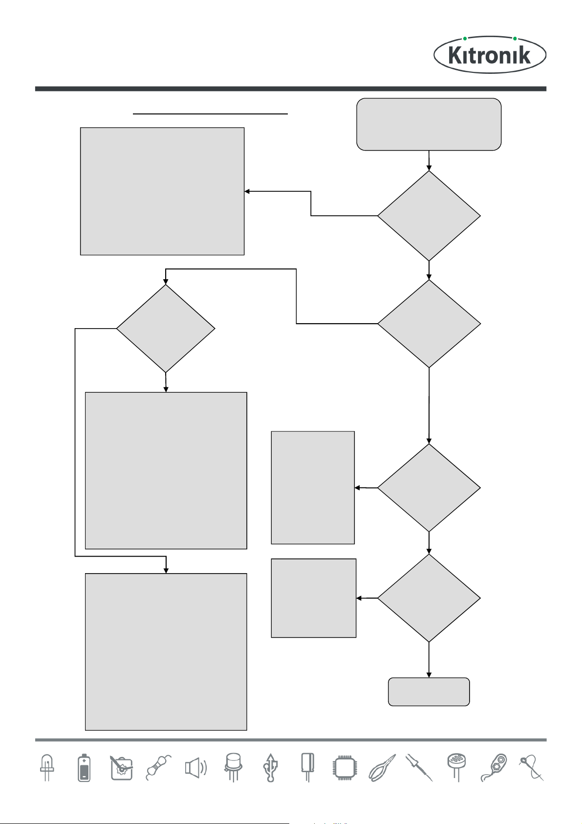
Fault finding flow chart
Fault Finding
Check
IC1 is in the right way around
For dry joints on the power
connectors
The input connector is in the
right place and the red and black
wire are the correct way around
IC1 for dry joints on pins 2 & 4
C3 and IC1 pins 3 & 4 for shorts
Speaker 1
Which
speaker is
their no sound
from?
Speaker 2
Start
Power up the board with it
connected to a music source
No
No
Are the speakers
making any kind
of sound?
Yes
Is the sound
coming out of
both speakers?
Yes
Check
The wire connections on speaker
2 for dry joints on the PCB and
speaker
The black jack wire is in the Blk
Input connection and In2 for a
dry joint
R6, C5 & IC1 pins 3 & 6 for dry
joints
R2 is in the correct place
C2 and IC1 pins 2 & 3, 5 & 6
for shorts
Check
The wire connections on speaker
1 for dry joints on the PCB and
speaker
The black jack wire is in the Blk
Input connection and In1 for a
dry joint
R5, C4 & IC1 pins 1 & 7 for dry
joints
R1 is in the correct place
C1 and IC1 pins 1 & 2, 7 & 8
for shorts
Check
The black
jack wire,
R1& R2 for
dry joints
R1, R2, R3 &
R4 are in the
correct place
Check
For a dry joint
on C1, R2 or
IC1 pins 5 &
6
No its
loud or
distorted
Yes
Is the speaker
playing the music
clearly?
Yes
Is one of
the speakers very
quiet?
No
Stop
Page 6
Stereo Amplifier Essentials
www.kitronik.co.uk/2136
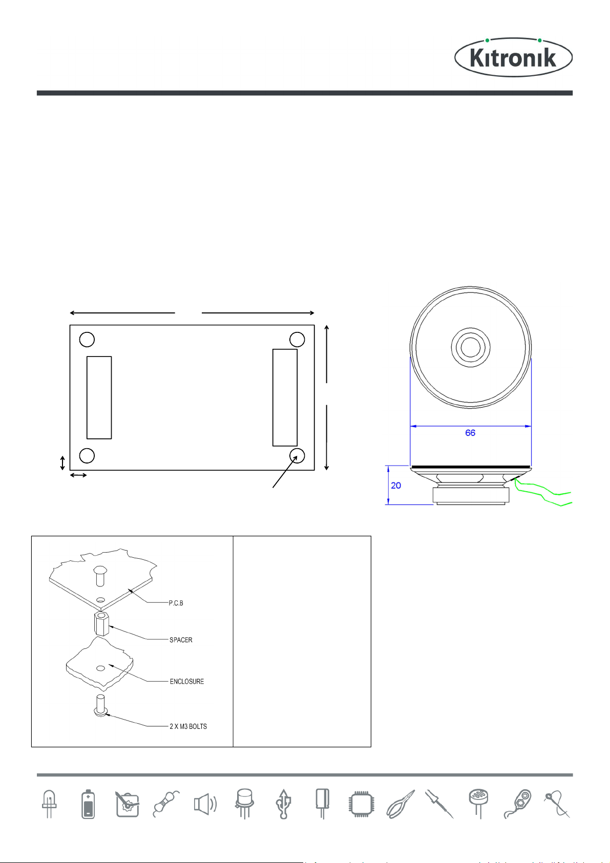
Designing the Enclosure
When you design the enclosure, you will need to consider:
The size of the PCB (below left, height including components = 15mm).
How big the batteries are.
How to mount the two speakers (below right).
How to allow the audio cable out of the box.
Are you making the amplifier for a particular MP3 player, if so should the MP3 player go in the box?
These technical drawings of the amplifier PCB and speaker should help you to plan this.
58
35
Speaker outputs
Audio & power inputs
4
4
4 x 3.3mm diameter mounting holes
Mounting the PCB to the
enclosure
The drawing to the left
shows how a hex spacer
can be used with two bolts
to fix the PCB to the
enclosure.
Your PCB has four
mounting holes designed to
take M3 bolts.
Page 7

Stereo Amplifier Essentials
www.kitronik.co.uk/2136
How the Amplifier Works
Out 1
Out 2
C4
470F
C5
Speaker 1
Battery
(15V max)
Input
R5
100K
R6
100K
TDA2822
In 1 +
In 1 -
In 2 +
In 2 -
470 F
C3
10 F
C6
100nF
C7
100nF
Speaker 2
C1
R1
10K
R2
100 FC2100 F
10K
R3
4R7
R4
4R7
At the centre of the circuit is an audio amplifier Integrated Circuit or IC. Inside the IC are lots of transistors, which are
connected together to allow the small input signal to be amplified into a more powerful output that can drive a
speaker.
All amplifiers need to use feedback to ensure that the amount of gain stays the same. This allows the output to be an
exact copy of the input, just bigger. The gain is the number of times bigger the output is compared to the input. So if
an amplifier has a gain of 10 and there is 1 volt on the input, there will be 10 volts on the output. An operational
amplifier has two inputs, these are called the inverting (-) and non-inverting (+) inputs. The output of the operational
amplifier is the voltage on the non-inverting input less the voltage on the inverting input, multiplied by the
amplifier’s gain. In theory, an operational amplifier has unlimited gain so if the non-inverting input is a fraction
higher than the inverting input (there is more + than -), the output will go up to the supply voltage. Change the
inputs around and the output will go to zero volts. In this format the operational amplifier is acting as a comparator,
it compares the two inputs and changes the output accordingly.
Amplifier
X10 gain
Output
With an infinite gain the amplifier is no good to amplify audio, which is where the
feedback comes in. By making one of the inputs a percentage of the output the
90%
10%
gain can be fixed, which allows the output to be a copy of the input but bigger.
Now when the two inputs are compared and the output is adjusted, instead of it
going up or down until it reaches 0 volts or V+, it stops at the point when the two
Input
inputs match and the output is at the required voltage.
Looking at the circuit diagram for the audio amplifier – it’s not obvious where the feedback is, this is because it is
inside the IC. The TDA2822M or NJM2073D chip has fixed the gain so the output is about 90 times bigger than the
input. To make the gain useful in our application, there is a potential divider on each channel that is fed into the IC
(R1+R5 and R2+R6). Each of these reduces the input signal to only 10% of the original signal. This, therefore, reduces
the overall gain of the amplifier to about 9 times the input to the circuit.
C3 is connected across the supply to make sure that it remains stable. The other capacitors have a filtering role,
either to cut out high frequency noise or get the best out of the speaker.
Page 8

Online Information
This kit is designed and manufact
ured in the UK by Kitronik
Two sets of information can be downloaded from the product page where the kit can also be reordered from. The
‘Essential Information’ contains all of the information that you need to get started with the kit and the ‘Teaching
Resources’ contains more information on soldering, components used in the kit, educational schemes of work and so
on and also includes the essentials. Download from:
www.kitronik.co.uk/2136
Every effort has been made to ensure that these notes are correct, however Kitronik accept no responsibility for
issues arising from errors / omissions in the notes.
Kitronik Ltd - Any unauthorised copying / duplication of this booklet or part thereof for purposes except for use
with Kitronik project kits is not allowed without Kitronik’s prior consent.
 Loading...