

Page 1
Page 2

TR850 Service Manual
Contents
1. OVERVIEW ............................................................................................................................................... 1
COPE OF MANUAL .................................................................................................................................. 1
1.1. S
AFEY PRECAUTIONS .............................................................................................................................. 1
1.2. S
2. PRODUCT CONTROL S AND LE D INDICATOR INTRODUCTION ........................................................ 2
RODUCT CONTROLS .............................................................................................................................. 2
2.1. P
2.2. LED
INDICATOR ....................................................................................................................................... 3
3. CIRCUIT DESCRIPTION .......................................................................................................................... 3
3.1. RF
3.1.1.
CIRCUIT ............................................................................................................................................. 3
Tx Circuit .................................................................................................................................................................. 4
3.1.2. RF Power Amplifier Module Circuit .................................................................................................................... 5
3.1.3. Rx Module Circuit ................................................................................................................................................... 6
3.2. GPS CIRUIT ............................................................................................................................................ 8
ASEBAND SECTION ................................................................................................................................ 9
3.3. B
Circuit Descrip ti on .................................................................................................................................................. 9
3.3.1.
3.3.2. Power Section ....................................................................................................................................................... 11
3.3.3. Audio Processing ................................................................................................................................................. 14
3.3.4. Ethernet Interface ................................................................................................................................................. 15
3.3.5. Boot Mode .............................................................................................................................................................. 15
3.3.6. Hardware V ers ion Enc ode ................................................................................................................................. 16
3.3.7. Baseband Board Interf ace and Indicator ........................................................................................................ 17
3.3.8. Tx Unit Interface Definition (J17) ...................................................................................................................... 18
3.3.9. RF Power Amplifier Module Interface (J18) ................................................................................................... 19
3.3.10.Rx Unit Interface D efinition (J15) .................................................................................................................... 20
3.3.11.Front Panel Interface Definition (J19) ............................................................................................................. 22
3.3.12.Serial Port Defin ition (J23) ................................................................................................................................ 22
3.3.13.JTAG Simulator Interface Def in it io n ( J 2) ....................................................................................................... 23
3.3.14.External Inter fac e Definition (J9) ..................................................................................................................... 24
3.3.15.Case External Int er face Definition .................................................................................................................. 26
4. FUNCTION AND PARAMETER SETTING............................................................................................. 28
ONVENTIONAL FUNCTIONS ................................................................................................................... 28
4.1. C
ARAMETER SETTING ............................................................................................................................ 28
4.2. P
4.2.1.
Parameters setting ............................................................................................................................................... 29
4.2.2. Install CPSp user programming softw are ....................................................................................................... 29
5. ASSEMBLY A ND DISA SSEMBLY INSTRUCTION ............................................................................... 32
UPLEXER ASSEMBLY ............................................................................................................................ 32
5.1. D
ISASSEMBLY INSTRUCTION ................................................................................................................... 34
5.2. D
XPLODED VIEW .................................................................................................................................... 36
5.3. E
ONNECTION ......................................................................................................................................... 41
5.4. C
I
Page 3

TR850 Service Manual
6. ADJUSTMENT ........................................................................................................................................ 44
REPARATION ........................................................................................................................................ 44
6.1. P
6.2. M
6.2.1.
ETHOD OF MODULATION AND TEST ...................................................................................................... 44
Local Oscillator Adjustment ................................................................................................................................ 44
6.2.2. Tx Adjustment........................................................................................................................................................ 45
6.2.3. Rx Adjustment ....................................................................................................................................................... 47
7. MAIN TECHNICAL FUNCTIONS AND SPECIFI CATIONS ................................................................... 49
8. MAINTENA NCE A ND TEST EQUIPMENT ............................................................................................ 51
9. TROUBLESHOOTING ............................................................................................................................ 52
APPENDIX1 400-470MHZ UHF BAND SPARE PART LIST..................................................................... 55
ABLE1 PARTS LIST (RX MODULE SECTION) .................................................................................................. 55
T
ABLE2 PARTS LIST (TX MODULE SECTION) ................................................................................................... 65
T
ABLE3 PARTS LIST (POWER AMPLIFICATION SECTION) .................................................................................. 72
T
ABLE4 PARTS LIST (BASEBAND MAINBOARD) ................................................................................................ 76
T
ABLE5 PARTS LIST (FRONT PANEL) .............................................................................................................. 84
T
ABLE6 PARTS LIST (POWER BOARD) ............................................................................................................ 84
T
ABLE7 PARTS LIST (ACCESSORY BOARD) ..................................................................................................... 85
T
IGURE 1 RX MODULE TOP BOARD PCB VIEW............................................................................................... 86
F
IGURE 2 RX MODULE BOTTOM BOARD PCB VIEW ........................................................................................ 87
F
IGURE 3 TX MODULE TOP BOARD PCB VIEW ............................................................................................... 88
F
IGURE 4 POWER AMPLIFIER MODULE TOP BOARD PCB VIEW ....................................................................... 88
F
IGURE 5 POWER AMPLIFIER MODULE BOTTOM BOARD PCB VIEW ................................................................ 89
F
IGURE 6 BASEBAND MAINBOARD TOP BOARD PCB VIEW ............................................................................. 90
F
IGURE 7 BASEBAND MAINBOARD BOTTOM BOARD PCB VIEW ....................................................................... 91
F
IGURE 8 FRONT PANEL TOP BOARD PCB VIEW ............................................................................................ 92
F
IGURE 9 FRONT PANEL BOTTOM BOARD PCB VIEW ..................................................................................... 92
F
IGURE 10 POWER BOARD TOP BOARD PCB VIEW ........................................................................................ 93
F
IGURE 11 ACCESSORY BOARD TOP BOARD PCB VIEW ................................................................................. 94
F
IGURE 12 ACCESSORY BOARD BOTTOM BOARD PCB VIEW .......................................................................... 94
F
IGURE 13 RX MODULE SCHEMATIC DIAGRAM ............................................................................................... 95
F
IGURE 14 TX MODULE SCHEMATIC DIAGRAM ............................................................................................. 102
F
IGURE 15 POWER AMPLIFIER MODULE SCHEMATIC DIAGRAM ..................................................................... 107
F
IGURE 16 BASEBAND MAINBAORD SCHEMATIC DIAGRAM ............................................................................ 110
F
IGURE 17 FRONT PANEL SCHEMATIC DIAGRAM........................................................................................... 125
F
IGURE 18 POWER BOARD SCHEMATIC DIAGRAM ........................................................................................ 126
F
IGURE 19 ACCESSORY SCHEMATIC DIAGRAM ............................................................................................. 127
F
APPENDIX2 136-174 MHZ VHF BAND SPARE P A RT LI ST .................................................................. 128
ABLE 1 PART LIST(RX MODULE SECTION) .................................................................................................. 128
T
ABLE 2 PART LIST(TX MODULE SECTION) .................................................................................................. 145
T
ABLE 3PART LIST(POWER AMPLIFICATION MODULE SECTION) ..................................................................... 151
T
II
Page 4

TR850 Service Manual
TABLE 4 PART LIST(BASEBAND BOARD) ....................................................................................................... 155
ABLE 5 PART LIST(FRONT COVER) ............................................................................................................. 163
T
ABLE 6 PART LIST(POWER BOARD) ............................................................................................................ 163
T
ABLE 7 PART LIST(ACCESSORY BOARD) ..................................................................................................... 164
T
IGURE 1 RX MODULE TOP BOARD POSITION MARK DIAGRAM ...................................................................... 165
F
IGURE 2 RX MODULE BUTTOM BOARD POSITION MARK DIAGRAM ............................................................... 166
F
IGURE 3 TX MODULE TOP BOARD POSITION MARK DIAGRAM ...................................................................... 167
F
IGURE 4 POWER AMPLIFIER MODULE TOP BOARD POSITION MARK DIAGRAM .............................................. 167
F
IGURE 5 POWER AMPLIFIER MODULE BUTTOM POSITION MARK DIAGRAM ................................................... 168
F
IGURE 6 BASEBAND MAINBOARD TOP BOARD POSITION MARK DIAGRAM .................................................... 169
F
IGURE 7 BASEBAND MAINBOARD BUTTOM BOARD POSITION MARK DIAGRAM ............................................. 170
F
IGURE 8 FRONT PANNEL TOP BOARD POSITION MARK DIAGRAM ................................................................. 171
F
IGURE 9 FRONT PANNEL BUTTOM BOARD POSITION MARK DIAGRAM .......................................................... 171
F
IGURE 10 POWER BOARD TOP BOARD POSITION MARK DIAGRAM .............................................................. 172
F
IGURE 11 ACCESSORY BOARD TOP BOARD POSITION MARK DIAGRAM ........................................................ 173
F
IGURE 12 ACCESSORY BUTTOM BOARD POSITION MARK DIAGRAM ............................................................. 173
F
IGURE 13 RX MODULE SCHEMATIC DIAGRAM .............................................................................................. 174
F
IGURE 14 TX MODULE SCHEMATIC DIAGRAM ............................................................................................. 181
F
IGURE 15 POWER AMPLIFIER MODULE SCHEMATIC DIAGRAM ..................................................................... 186
F
IGURE 16 BASEBAND MAINBOARD SCHEMATIC DIAGRAM ............................................................................ 189
F
IGURE 17 FRONT PANNEL SCHEMETIC DIAGRAM ........................................................................................ 204
F
IGURE 18 POWER BOARD SCHEMETIC ....................................................................................................... 205
F
IGURE 19 ACCESSORY SCHEMATIC DIAGRAM ............................................................................................. 206
F
III
Page 5

TR850 Service Manual
1. Overview
1.1. Scope of Manual
This manual is intended for use by trained engineers and professional technicians for the maintenance
and repair of TR850 Repeater. Data changes in this manual may occur with the improvement of
technology. To get the latest technology information, please contact us or your l oc al d ist ributors.
Before repairing the unit, please read this manual.
1.2. Safey Precautions
Electromagnetic Radiation
Radios generate and radiate electromagnetic energy, the security design of Kirisun radios’
electromagnetic radiat ion on human meets national and international standards.
Electromagnetic Interference
Installation should be i n accordance with local radio regulations.
Explosive and Harmful Gases
Do not install the repeater in areas with explosive and harmful gases, such as the lower deck of the hull,
fuel or chemical storage faci lities, area where the air contains chemicals or particles, dust or metal dust.
Do not install the repeat er when close to the blasting area, electric blasti ng detonators.
Replacement Parts
When replacing any replacement part, please be aware of the model. Do not arbitrarily replace the
component that does not matc h with the radio.
1
Page 6
TR850 Service Manual
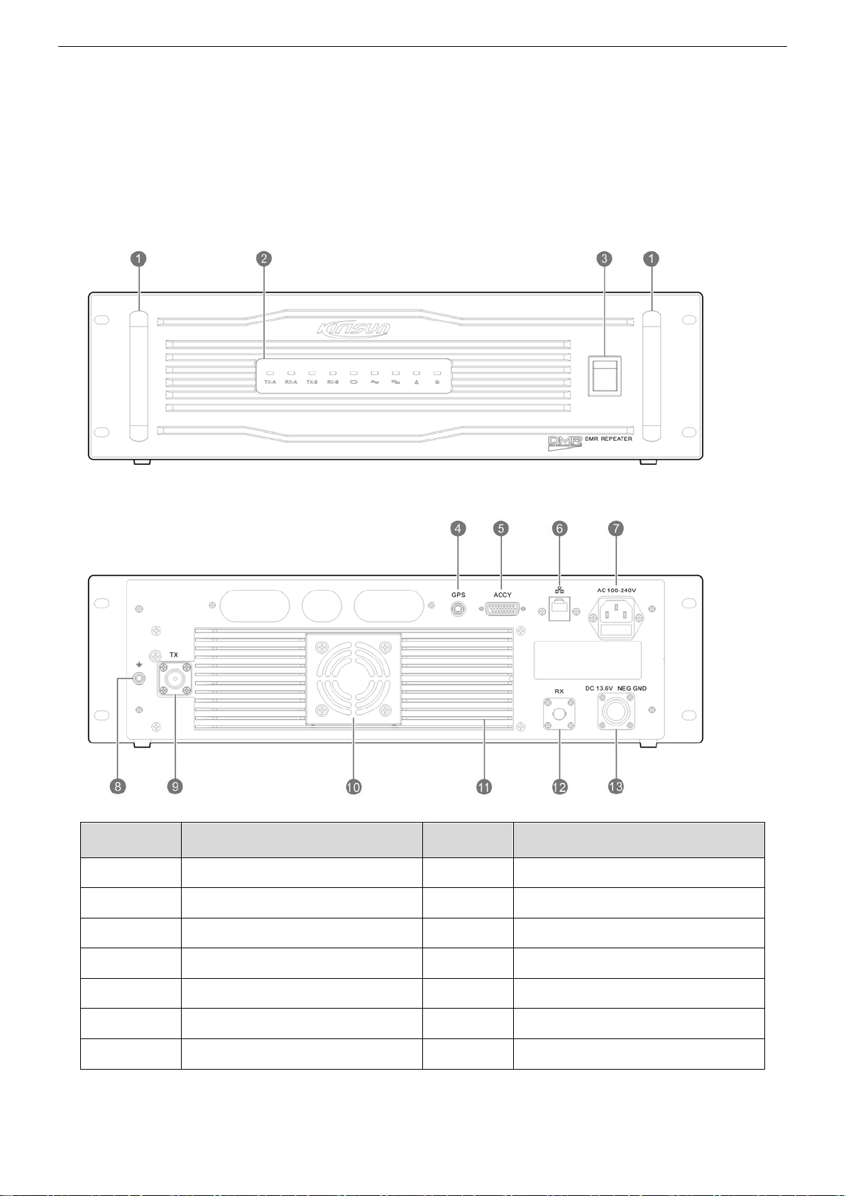
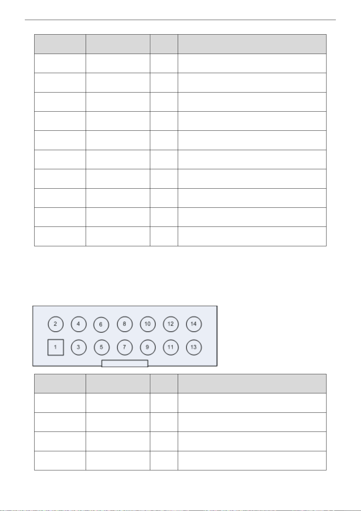
2. Product Controls and LED Indicator
Introduction
2.1. Product Controls
No. Part Name No. Part Name
1 Handle 2 Front Panel LED Indicator
3 Power Switch 4 GPS Atenna Co nnector
5 ACCY Connector 6 Internet Connector
7 AC Connector (with fuse) 8 Grouding Scew
9 Transmit Ante nna Connector (N) 10 Fan
11 Heat Sink 12 Receive Antenna Connector (BNC)
13 DC Connector - -
2
Page 7
TR850 Service Manual
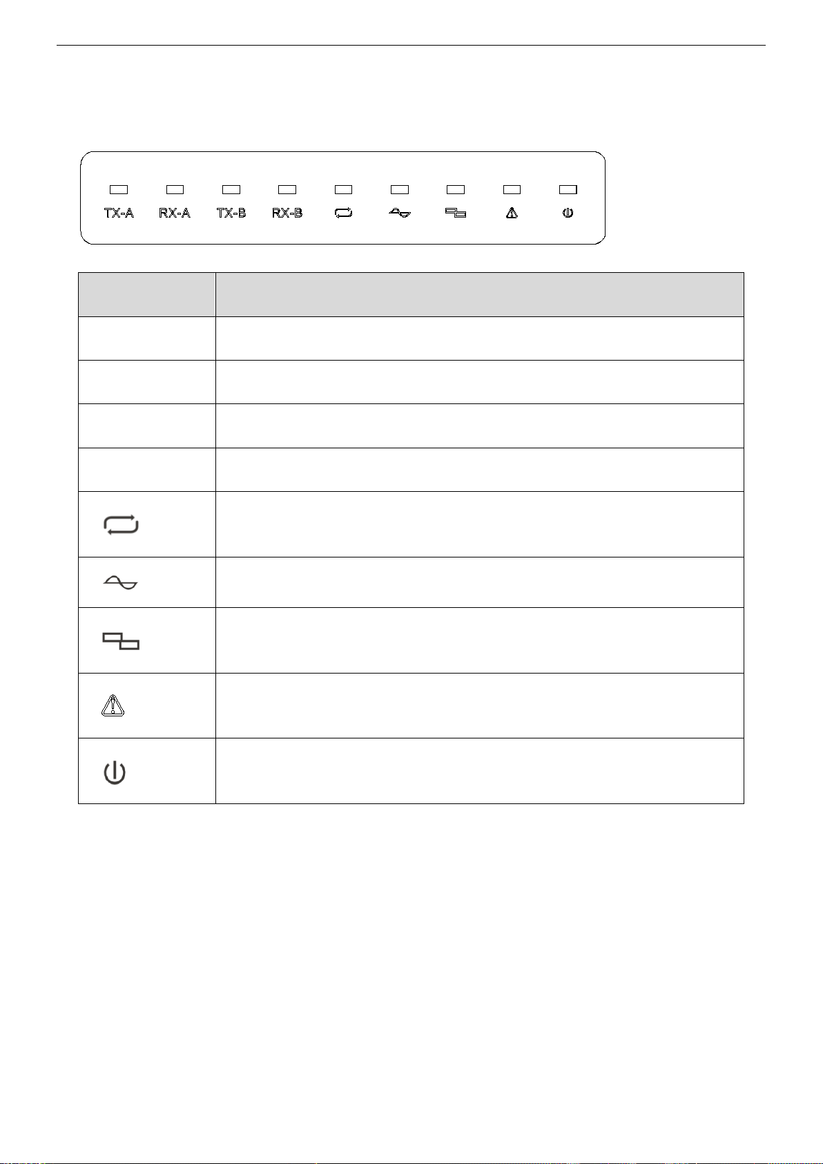
2.2. LED Indicator
LED Description
TX-A Indicates slot 1 is transmitting.
RX-A Indicates slot 1 is receivin g.
TX-B Indicates slot 2 is transmitting.
RX-B Indicates slot 2 is receivin g.
Repeater mode. When illuminated, the repeater is active. When the
repeater is inactive, the LED is o ff.
Analog mode. For analog or mixed signals the LED flashes when active.
The LED is off when inactive.
Digital mod e . F or di gi tal or m ix e d signals the LED flashes when active. The
LED is off when inactive.
Alarm mode. Illuminates when there is a problem with the repeater.
Illuminates when the repeater is switched on.
3. Circuit Description
3.1. RF Circuit
The RF part is compos ed of transmitter module, power amplifier mod ul e and receiver module.
3
Page 8
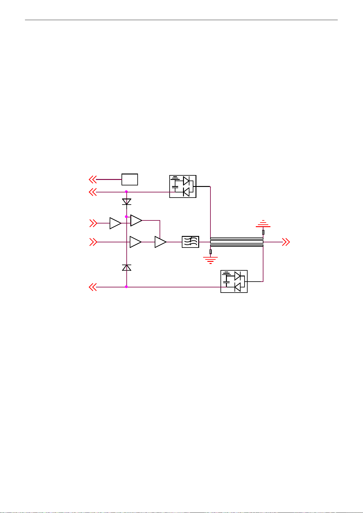
3.1.1. Tx Circuit
X100
MODE1
SDATA
TXPLLCS
SCLK
TXLD
MODEIN
Q2002
IC100 SKY72310
IC306
U402
TOTXPA
MODE2
TXVCOSELECT
TXVCO1+TXVCO2
Q105
Q106
TXENABLE
Figure 3-1 Transmitter Circuit
TR850 Service Manual
Transmitter circuit includes three parts:
Two Point Modulation Circuit
The RF center frequency cal ibrat ion from the baseband and the low frequency part of 4FSK signal will
be processed with addition algor it hm, then sent to the DAC to get MODE1 signal. The MODE1 directly
enters the reference cloc k X100, which is used for cent er frequenc y control a nd low fre quency modulation.
The MODE2 signal, which passes the two-level low pass filter which is composed of IC301s for DAC
sampling interference filter , will be sent into VCO for high frequency part modulation.
Transmitter Frequency Generation Unit Circuit
The transmitter PLL includes two VCOs,one PLL(IC100) IC SKY72310 and reference clock X100. The
transmitting frequencies of the two VCOs controlled by the TXVCOSELECT signal are 400~435M Hz a nd
435~470MHz respectively.(VHF is 136~ 155MHz and 155~174MHz)
a. Working Principle of Voltage Controlled Oscillator
The Tx Module employs two VCOs which cover the band of 400~435MHz and 435~470MHz (VHF is
136~155MHz and 155~174MHz). The switch of VCO is controlled by the TXVCOSELECT signal. VCO
employs thr ee point capac itanc e oscillation circuit. The VCO that c overs the band of 40 0~435M Hz (VHF is
136~155MHz) is composed of D106~D109、L119、Q106 and some other components, while the VCO
covers the band of 435~470MHz (VHF is 155~174MHz) is composed of D101~D104、L107、Q105 and
some other components .
The 12.8 MHz reference clock (X100) output signal which is controlled by MODE1 signal will enter the
reference input port of PLL IC (IC100 SKY72310), then according to the configuration of register, it will be
divided to get 3.2MHz reference frequency, and the frequency will be compared in phase difference with
the signal generated by t he frequenc y div ision which is resulted from the VCO’s enter into the input port of
PLL chip. The PLL (IC100 SKY72310) PD pin will output the positive or negative pulse current which is in
b. Working Principle of Frequency Generation Unit
output pulse width, is directly proportional to the aforementioned signal phase difference. When the pulse
4
Page 9
TR850 Service Manual
D103
SWR-R
IC100
POWERCONTROL
IC101
DS18B20
RFOUT
SWR-T
Q102
RF IN
U100
D104
current passes the loop f ilter, it will be converted to CV voltage via RC integral. The the CV voltage will be
sent to the VCO varactor to adjust and control the output frequency from the VCO until the CV voltage
becomes constant. The loop is locked in the meantime.
Buffer Amplifier Circuit
VCO outputs the modulated carrier signal to enter Q2002 for buffer amplication and then passes the LPF
U402 to eliminate the harmonic wave. A fter that, the signal will go into IC306 for pre-amplification, then
passes the LPF to filter the harmonic wave again, and the signal is output to the SMA connector which is
connected to the transmitt ing power amplification.
3.1.2. RF Power Amplifier Module Circuit
Figure 3-2 RF power amp lification module
The power amplifier module will amplify the modulated carrier signal from the transmitter module to a
certain power level, t hen send to the transmitter port.
The power amplifier modu le includes the three parts:
Power Amplification Part
The modulated carrier from the transmitter module will enter Q102 for pre-amplification, then the signal
will attenuate to a certain level to make the amplitude of the signal which will be input with U100 operates
between 17~20dBm. Under the control of POWERCONTROL signal, the RF signal output from U100 will
pass the LPF to suppress the harmonic wave and collect power stationary wave sample from the
directional coupler before being sent to the antenna port.
APC and Stat ion ar y Wave Protection Circuit
The directional coupler detects the forward and reverse directions RF signal and passes the Q103,Q104
to convert the signal to the DC voltage which is corresponding to the forwardand reverse direction power.
After the voltage division, the forward direction DC voltage with the reverse direction voltage pass the
selection switch which is composed of D201,D202 and enter IC100(NJM2904) for buffer amplification
before being sent to the reverse phase input port of the operational amplifier of IC100(NJM2904). The
5
Page 10
TR850 Service Manual
IC6003
FS
DATAOUTB
CLK
DATAOUTA
IC6001
AD9864SYNCB
IC1000
Q1009/1011
U5002
Q2002
PD
PC
PE
PLL
PLL CONFIG
12.8MHz
BPF AD J U ST
IC3000
L3006/8/9
L3000/1/2
Z3001
IC3005
L3010/11/12
Z3000
Q3001/2
U4000 AD9864
2rd LO
18MHz CLOCK
IC3003
RXVCOSELECT
POWERCONTROL control signal form the baseband will be sent to the identical phase input port of
IC100(NJM2904)’s operational amplifier. After the operational amplification and external circuit’s function
calculation, the signal is output as a conrol signal which controls the U100 gain control port to ensure that
the actual output power remains stable when the impedance matches and to decrease the output power
for power amplifier protection when the impedanc e mismatches.
Temperature Detection Circuit
The continuous temperature rise can lead to a decrease of transmitting power. The temperature detection
employs IC101(DS18B20) to collect the digital temperature sample.W hen the temperature exceeds the
threshold value, the fan wi ll be switched on for heat dissipation.
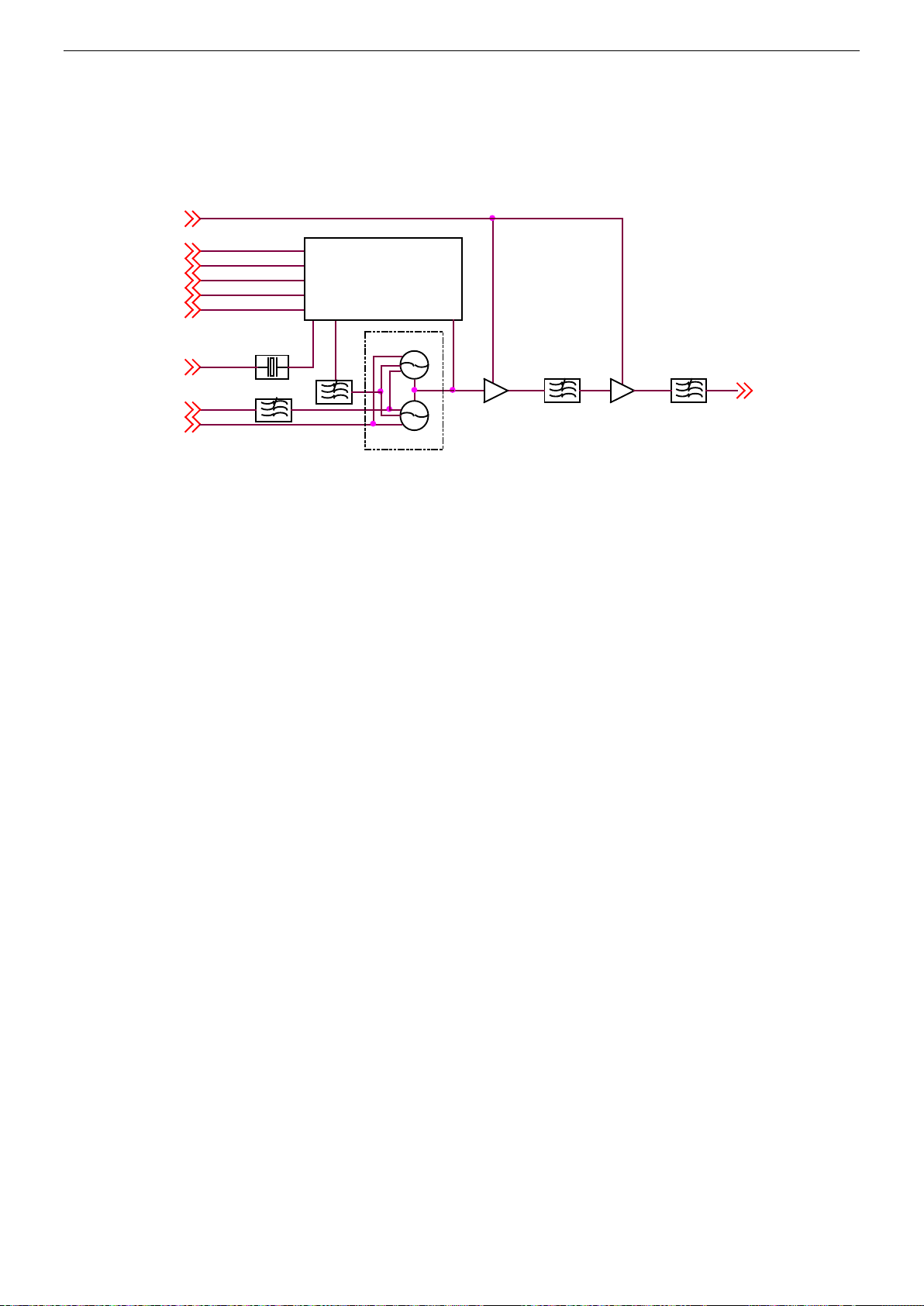
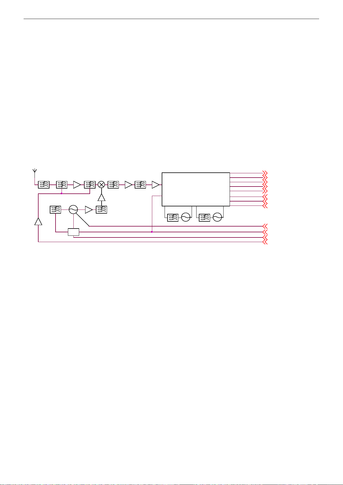
3.1.3. Rx Module Circuit
Figure 3-3 Receiver Module
Receiver Circu it
The receiver circuit includes RF Band pass filter, Low-noise amplifier, mixer, IF filter, IF ampli fier and IF
processor.
The signal from the receiving port first passes the low pass filter to suppress the high frequency
interference, and passes the electrical tuning BPF to suppress the image interference and the out-band
interference.The in-band signal is sent to the low noise amplifier (IC3000) and the amplified signal passes
the electrical tuning BPF contr olled by BPFADJUST to filter t he out-ba nd interf erence, so the ef fect ive high
frequency will be sent to the mixer(IC3005). Meanwhil e, the first loc al oscillation passes the LPF and gets
mixed with the effective signal in IC3005 to generate the first IF signal (51.65MHz). The first IF signal
passes the crystal filter (Z3001) to suppress the out-band signal. The signal is then sen t to IF amplif ier
(IC6003) for amplification before being sent to the crystal filter to strenghthen the suppression of the the
adjacent channel. After being sent to the limiting amplifier composed of Q3001 and Q3002, the signal
enters AD9864 (U4000) for the second freq uency mixing ,IF amplification and AD sampli ng. The digital IQ
signal will be finally output to the baseband for further processing.
6
Page 11
IF Processor Circuit
Figure 3-4 IF Processor
TR850 Service Manual
The 51.65MHz IF signal output from the IF amplifier enters the AD9864 via its pin 47, and it finishes the
second frequency mixing in the AD9864 to convert the fisrt IF to the second IF. The second IF signal is
converted to the digital signal through the ADC sampling and output from the SSI port, and the digital
signal is sent to FPGA f or demodulation.
The reference frequency of AD9864 is 12.8MHz. The second local oscillation VCO is composed of
external oscillation tube, varactor, and related components. The VCO provides the 49.4MHz local
oscillation signal. The clock frequency of AD9864 is18MHz and it is generated by external LC resonance
circuit.
Rx Module Frequency Generation Unit C irc uit
The Rx Module Frequency Generation Unit Circuit is composed of two VCOs and one PLL. Two VCOs
cover the band of 400~435M Hz and 435~470MHz respectively (VHF is 136~155MHz and 155~174MHz).
a. Working Principle of PLL
The 12.8MHz clock frequency provided by the baseband will enter the frequency divider for division, and
then the 3.2MHz phase detecting frequency will be generated. The signal generated by VCO enters the
PLL chip for frequency division, and goes into the PD to get compared in phase difference with the signal
generated by frequency division of reference clock, thus the continuous pulse current is generated. The
continuous pulse current p asses t he loop filter and w ill be conv erted t o CV volt age via R C integral. The C V
voltage will be sent to the varactor, and it controls and adjusts the VCO output frequency until the CV
becomes constant. In the mean time, the PLL is locked, and the stable output frequency from VCO
passes the two buffer amplifier to enter the frequency mixer.
b. Working Principle of VCO
The Rx module employs two VCOs which cover the band of 348.35~383.35MHz and 383.35~418.35MHz
7
Page 12
TR850 Service Manual
(VHF is 84.35~103.35MHz and 103.35~122.35MHz) respectively, and the switch of VCO is controlled by
the RXVCOSELECT sign al. VCO employs three point capacitance oscillation circu it. The VCO that covers
the band of 348.35~383.35MHz (VHF is 84.35~103.35MHz) is composed of D1006~D1009、L1017、
Q1011 and some other components, while while t he VCO covers the band of 383.35~418.35MHz (VHF is
103.35~122.35MHz) is composed of D1002~D1005、L1016、Q1009 and some other components.
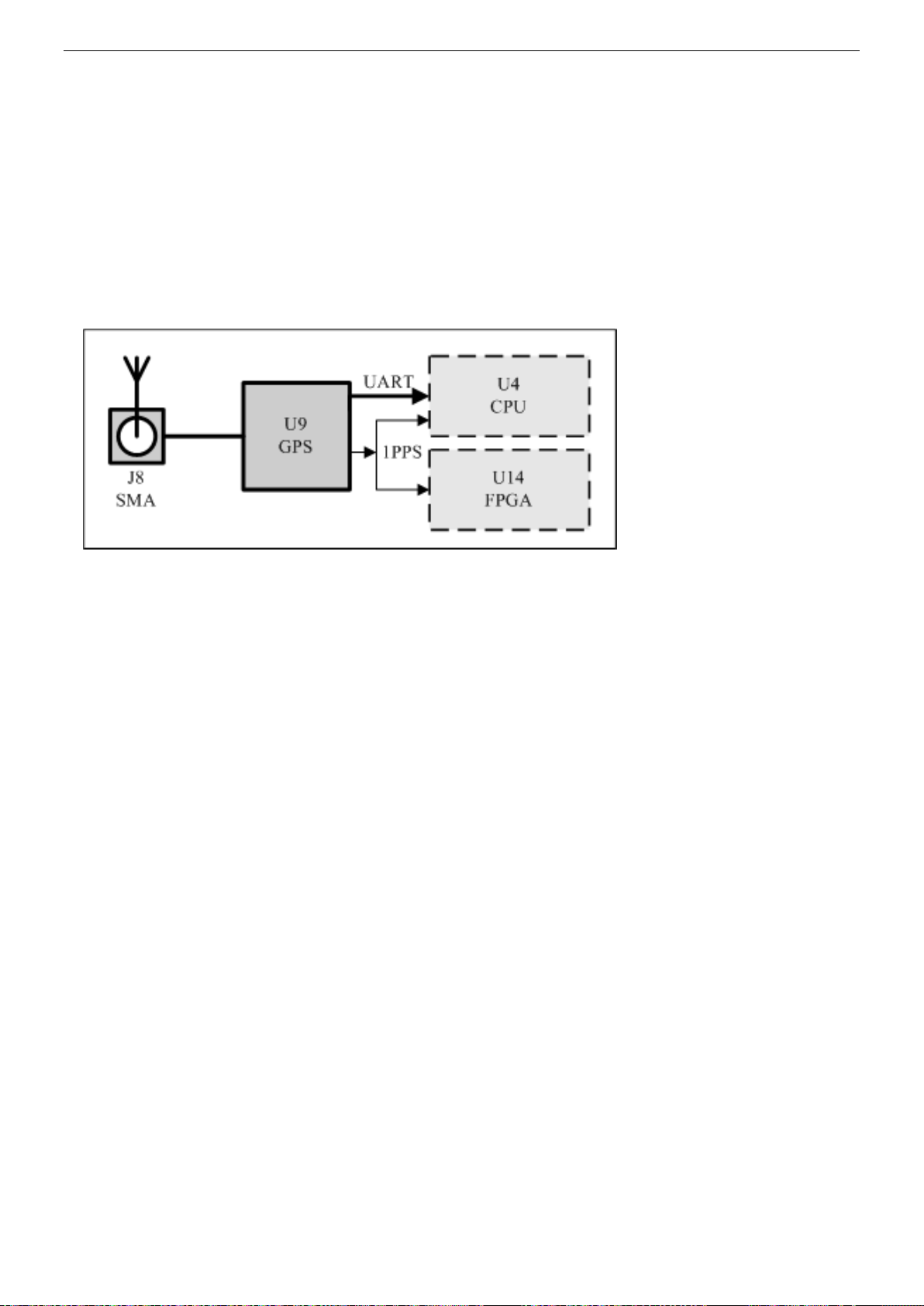
3.2. GPS Ciruit
Figure 3-5 GPS Schemat ic Diagram
As Figure 3-5 shows, the repeater baseband board includes the GPS module (U9) and the GPS an ten na
interface J8(SMA). The corresponding equipment box is also assembled with a GPS antenna interface
which supports the outdoor active antenna. The GPS module integrates a baseband processor, LNA and
SAW. The antenna receives the 1575.42M Hz GPS signal, a f ter t he inner a mpli ficati on and fi lter proce ss , it
will be sent to the baseband section for further calculating, to get the geographical location and time
information of the equipment. The output data information will be sent to processor (U4). M eanwhi le , the
GPS module hardware will provide the one-pulse-per-second signal (1PPS) for OMAP and FPGA
respectively.
8
Page 13
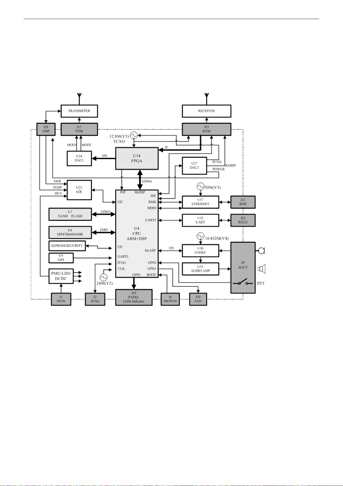
3.3. Baseband Section
3.3.1. Circuit Description
Figure 3-6 Baseband Circuit
TR850 Service Manual
As Figure 3-6 shows, inside the dotted line box is the baseband section circuits, which includes the four
major modules of dual core processor(U4), DDR2(U6), NAND FLASH(U7) and FPGA (U14). They are
used to run the Linux operation system with various drivers and protocols to achiev e call forwarding.
9
Page 14
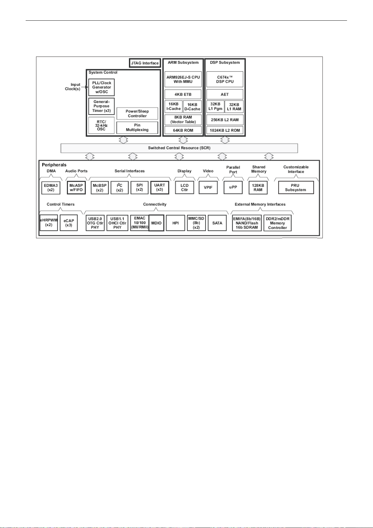
Figure 3-7 Processor Inter nal Circuit
TR850 Service Manual
The internal circuit of the proces sor is as Figure 3-7 shows, which is co mpos e d of variou s seri al inter fac es
such as 300MHz ARM926EJ MPU、300MHz C674x DSP、DMA controller、SDRAM EMIF interface、EMAC
Ethernet IC RMII interface、McASP digital audio interface and McBSP, SPI, I2C, UART.
U6 is DDR2 S DRAM wi th the capacity of 1Gb(64Mx16), and it is used to store the running program
codes and various dynamic data.
U7 is NAND FLASH with the capacity of 2GB, and it is used to store the drive rs of all the devices,
operation system and application program code wh ich includes the program code of FPGA.
The digital IF signal sent from the FPGA processing receiving unit communicate with the processor U4
via EMA BUS, and it communicate with DAC via the analog SPI interface to process the transmitting and
receiving data, which includes the data framing, filter, interpolation, extracting and etc. to achieve the
calculation and synchronization of frame number. The PLL module inside the FPGA IC will process the
external 12.8MHz, +/-1.5ppm reference clock to generate a 61.44MHz master clock via 24/5 frequency
doubling and frequency division.
The external circuit includes the parts of ADC, DAC, CODEC, AUDIO AMP, ETHERNET, RS232 and etc.
The Analog-Digital Convertor ADC (U22) collects data such as stationary wave signal detection and
power supply voltage detection which are controlled by RF power.
Digital-Analog Convertor DAC (U24) is used for transmitter two point modulation output, and the other
DAC(U27) is used to achieve the band pass adjusting and the RF power amplification control of the RF
receiver, the tuning control of the receiver local oscillation reference clock.
CODEC(U30) achieves the digital-analog converting. It is connected to the OMAP processor via I2S
digital audio interface to achieve the local monitoring, output and input of interposed speech or audio
10
Page 15
TR850 Service Manual
Tx/Rx index testing.
The output power of audio power amplifier (U31) is 1W, which is used for local monitoring or tested
speech output.
Network interface (U17) is the TRx components of 10/100M single Ethernet physical layer , and it is used
to the tuning of various parameter setting and communication control.
UART- Universal Asynchronous Receiver/Transmitter(U32)achieve s the RS232 electrical level switch,
when it communicates with the PC, it can initiate the programming burning, programming tuning
information printing, and e tc.
3.3.2. Power Section
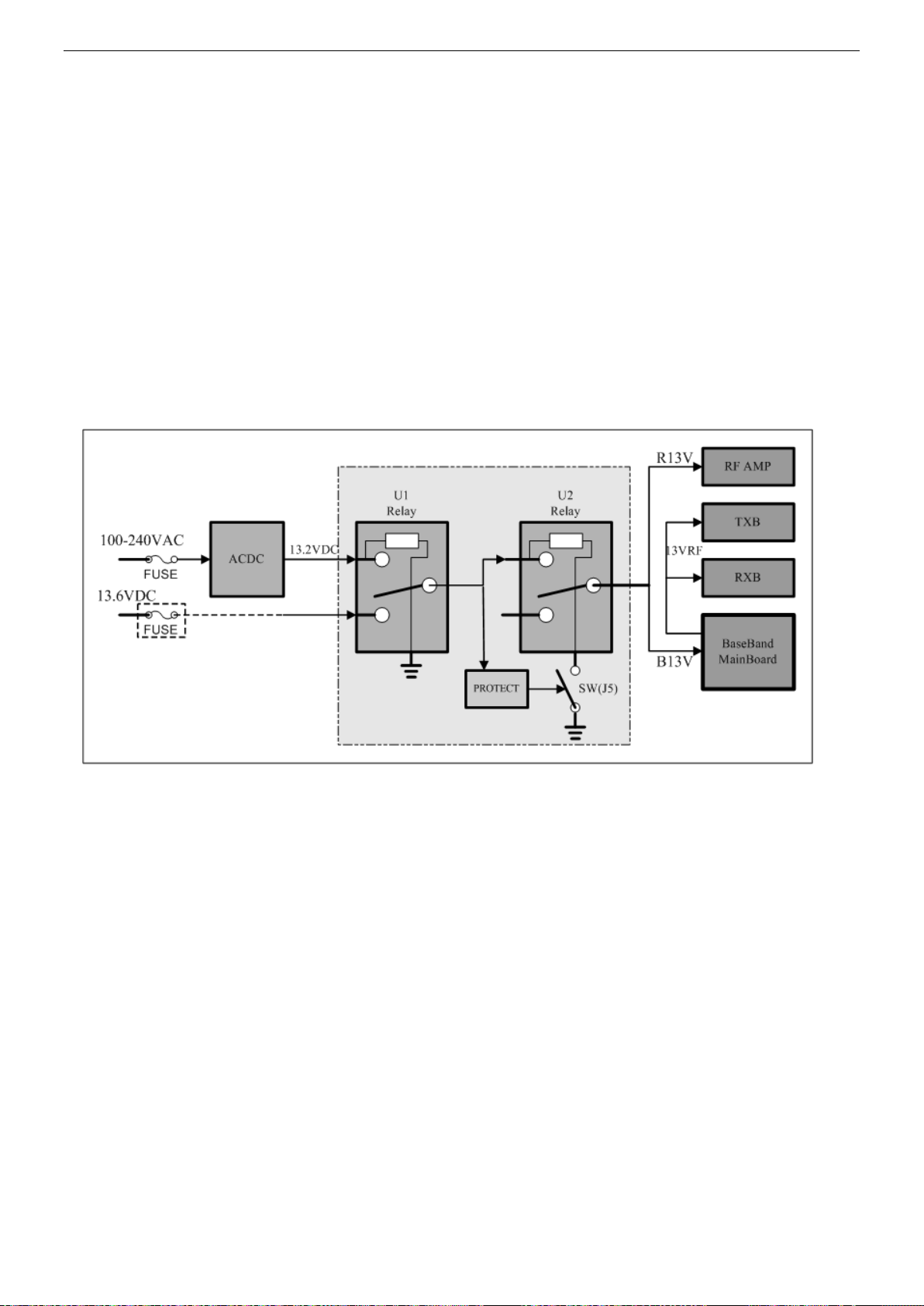
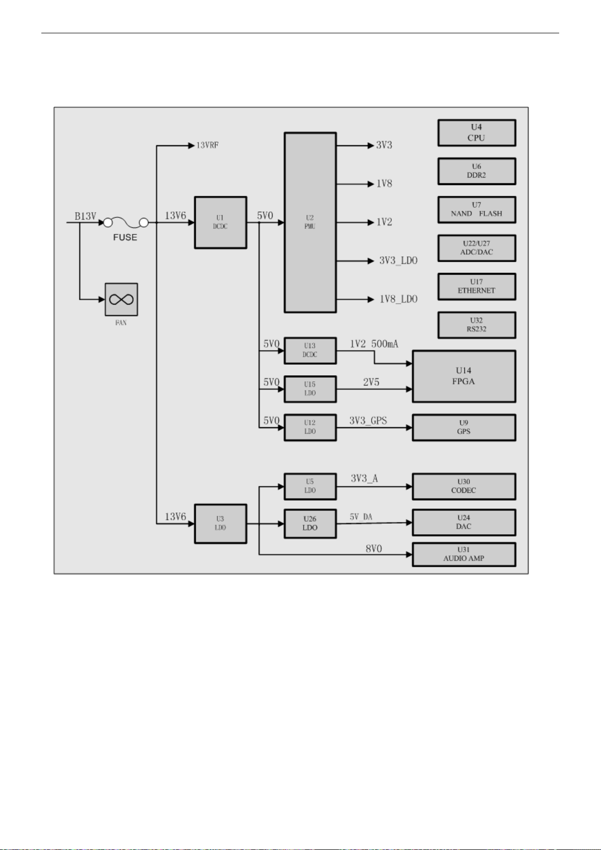
Figure 3-8 Whole Unit Power
As Figure 3-8 shows, the whole unit power supply employs adaptive ac/dc power supply with AC priority
and DC/AC auto switch. The output DC voltage which is switched and protected by the electric relay will
be divided into two paths. One path is for the RF power amplification, and the other is for banseband
mainboard. The switch in the front panel turns the power on/off via the electric relay U2. The protection
circuit wil l c u t off all the DC output when the DC exceeds 18V.
The AC/DC switching part employs an independent module power supply(320W), and it supports the AC
input range between 100V-240V, nominal output DC voltage is 12V, and the factory set is 13.2V.
The rated AC input voltage is between 100-240V, the socket is built in the dual protective tube.
Specification of the protective tube is 2.5A, 5x20mm cer amic tube, slow type.
The rated DC input voltage is 13.6V with the rated current being 15A. The protective tube is included in
the DC accessories.
Power Switch and AC/DC Switch
As the Figure 3-8 shows, t he elect ric re lay is sw itch ed on for t he AC power supply and it will cut off the DC
point. The 13.2VDC output from the ACDC m odule is c onnect ed to U2 thro ugh the U1 c ont a ct. If the panel
switch (J5) is on, the electric relay (U2) will be switched on, so is the repeater.
11
Page 16
TR850 Service Manual
When AC power supply is off, the electric relay (U1) is released. The DC is connected to U2 via the
electric relay (U1) contac t . I f t he panel switch (J5) is on, the electric relay U2 will be switch ed on, so is t he
repeater.
The panel switch (J5) is off, and U2 is released, which cut off the baseband DC power supply B13V
including the RF power supply R13V.
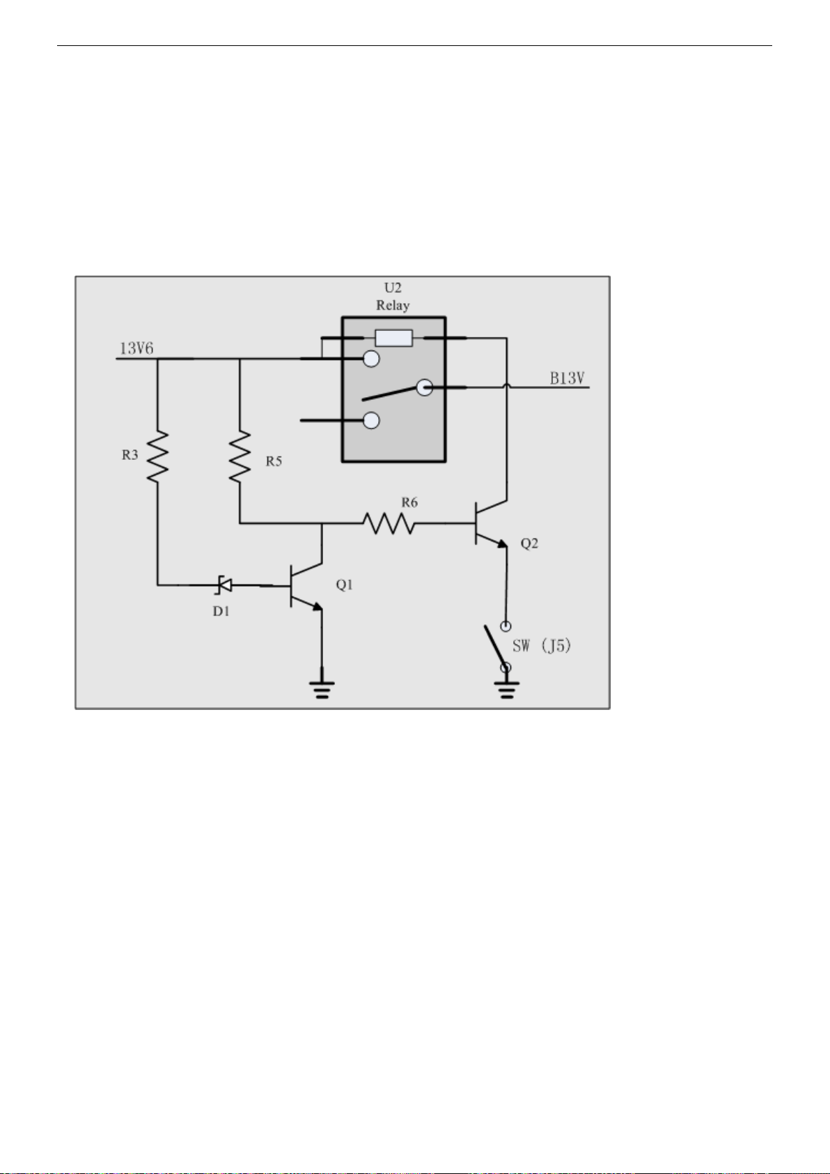
Over-voltage Prote ction
Figure 3-9 Over-voltage Circuit Protection
As the Figure 3-9 shows, the breakdown voltage of the voltage stabilizing diode is 18V+/-0.5V. If the input
DC volatage is over 18V+/-0.5V, the Q1 breaks over with Q2 being cut of f, and the electric relay U2 will be
released to cut off the DC power supply B13V, includ ing t he RF power supply R13V.
12
Page 17
TR850 Service Manual
Baseband Board Power Supply
Figure 3-10 Baseband Board Power Supply Distribution Diagram
As Figure 3-10 shows, the baseband and RF employs isolated power supply. B13V will be divided into
three paths. One path provides power for baseband circuit, the second one is provided for Tx and Rx
module af ter being isolated by magnetic bead, and the last one is provided for heat dissipation fan after
being isolated by the ferrit e Inductor.
The digital and analog part of the baseband circuit own separate power supply.
The power supply of the digital circuit is composed of two-level switch circuit. The first level decreases
the B13V to 5V via DC/DC (U1) ; the second level switches 5V to 3.3V, 1.8V, 1.2V and etc.. wh ich are
isolated by various magne t ic beads before being supplied to the circuit modul es.
The analog circuit power supply will be directly supplied to analog audio power amplification circuit after
being switched to 8V via LDO. One power path outputs 5V_DA via the low voltage LDO (U26) and
provide it for the analog power of DAC(U24, U27), and the other oupts 3.3V_A via the low voltage LDO
13
Page 18
TR850 Service Manual
(U5) and provide it for the analog p ow er of CODEC (U30).
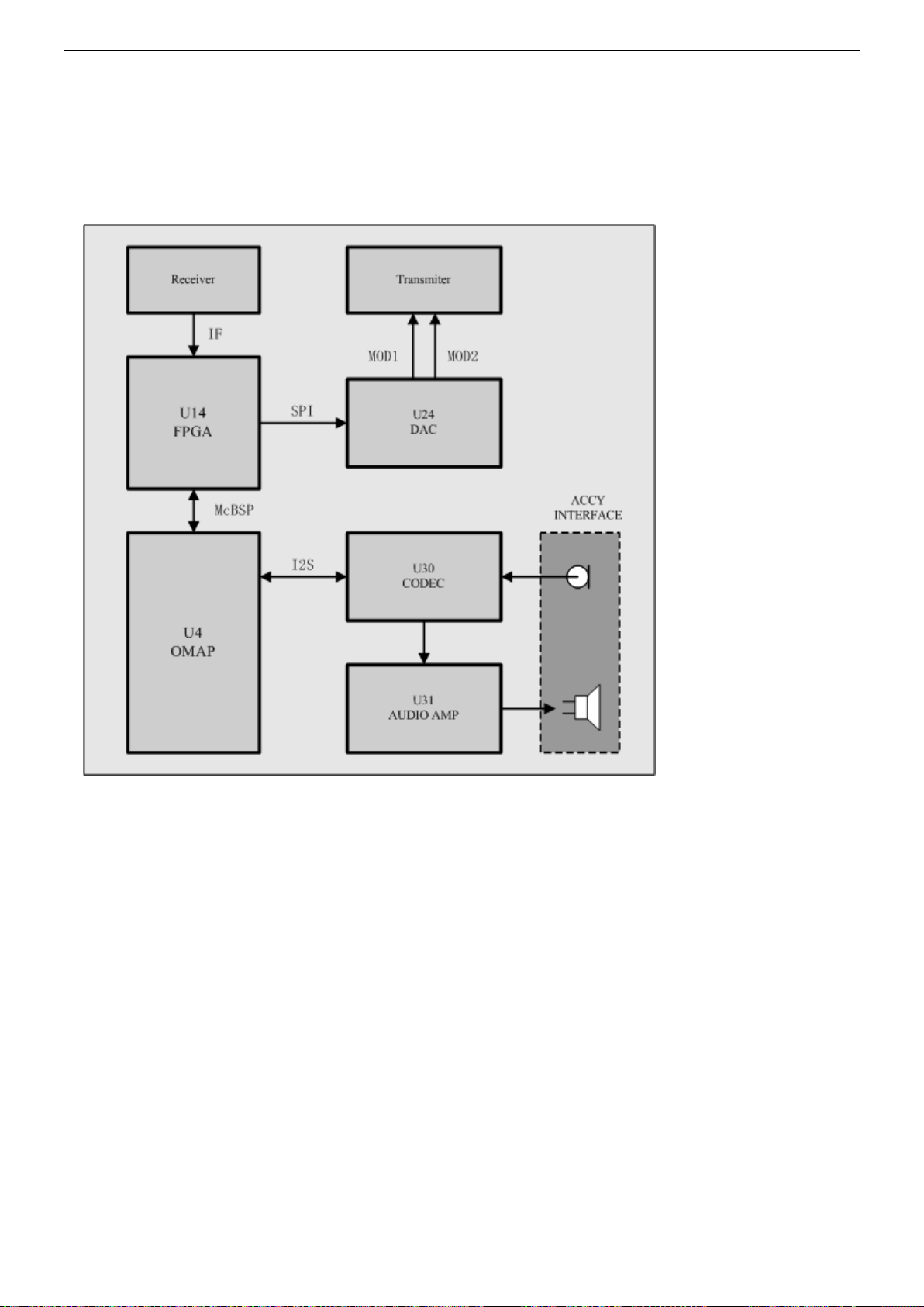
3.3.3. Audio Processing
Figure 3-11 Audio Proces s ing Schematic Diagra
As the Figure 3-11 shows, the audio processing module mainly achieves encoding and decoding with
ADC and DAC of the audio signal, including air audio forwarding and local audio TRx.
Air Audio Forwarding
The digi tal IF si gnal fr om the RF r ecei ver wil l be first sent to the FPGA(U14) for time slot processing and
achieving the framing, filtering and extracting of the data to realize the calculation and synchronization of
the frame number; the signal will be send to the DSP of CPU (U4)via the McBSP interface for 4FSK
decoding, digital audio signal decoding and etc.. Meanwhile, the internal DSP will send the digital audio
signal which achieves t he decodin g and enc oding to the FPGA(U14) for time slot processing and finishi ng
the framing, filtering and interpolation and other synchronization calculation of the data, and the digital
audio signal will then be sent to the DAC (U24) via the SPI interface for the audio digital/analog switch,
generating the analog speech two point modulation signal before being sent to the transmitter for the
audio forwarding.
Local Audio TRx
The internal DSP in the main processor(U4) connects to the CODEC(U30) via the I2S digital audio
interface. The CODEC(U30) will convert the analog audio input from the external to digital audio, then
14
Page 19

TR850 Service Manual
send into the internal DSP. In the meantime, converts the received digital audio from the internal DSP to
analog audio, then send t he audio t o audio pow er a mplifier( U31), be fore final ly send t o the ACCY external
interface, which is to drive the 1W, 16Ω speaker.
3.3.4. Ethernet Interface
Figure 3-12 Ethernet Interface
As Figure 3-12 shows, A RMII simpli fied interface is used between the CUP(U4) and network interface
chip(U17) . RMII inter fac e independent clock uses external clock mode and sh ar e 50MHz clock with U17.
CPU (U4) achieves the hardware information of internet interface U17 through the independent
configuration interface MDIO. CPU also initiate it and assi gn M AC and IP address.
The data transmitt ing and receiving bet ween netw ork inter face ch ip(U17) and interface connector(J12) are
achieved through connecting the transformer inside the connector jack RJ45 and LED through 2 pairs of
differential line.
The network interface can realize parameter adjustment and parameter conf igure, user programming and
firmware upgrade.
3.3.5. Boot Mode
A boot mode selection switch (J4) is provided on the baseband. The four position 1 to 4 of DIP encode
switcher are correspondingly connected with boot 1 to boot 4 of OMAP (U4), so the boot operation mode
will be changed after being powered on.
The level of position “ON” of encode switcher corresponding to boot which is connected to GND is
“0”.Conversely, the level of position “OFF” is “1”.
As showing in Figure 3-13, the level of boot1 to boot4 of switcher is 0101, and it enters to firmware
download mode after power on. It can upgrade the guide program and the low driver program by booting
from serial port(UART2).
15
Page 20
TR850 Service Manual
Figure 3-13 Firmware Download Mode Figure 3-14 User Mode
As showing in Figure 3-14, the level of boot 1 to boot4 is 1110, and it enters to normal running user mode
after power on. It starts from NAND FLASH. In this mode, it can upgrade operation system kernel, device
driver program, files syst em an d application program by network interfac e.
Please configure the boot mo de as user mode as shown in Figure 3-15 in normal use.
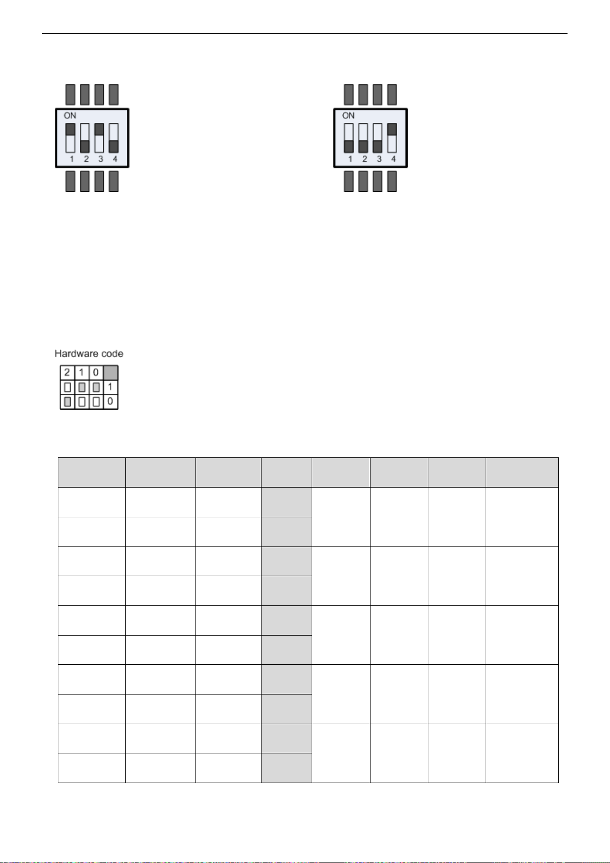
3.3.6. Hardware Version Encode
Figure 3-15 Hardware V er sion Enc ode
According to the position of chip resistor in Figure 3-15 the encoder is “001” and the corresponding
version is Ver3. 0.
2 1 0 D2 D1 D0 Version
NULL NULL 0R
0R 0R NULL
NULL 0R NULL
0R NULL 0R
NULL 0R 0R
0R NULL NULL
1
0 0 1 Ver1.0
0
1
0 1 0 Ver2.0
0
1
0 1 1 Ver3.0
0
0R NULL NULL
NULL 0R 0R
0R NULL 0R
NULL NULL NULL
1
1 0 0 Ver4.0
0
1
1 0 1 Ver5.0
0
16
Page 21
TR850 Service Manual
0R 0R 0R
1
1 1 0 Ver6.0
NULL NULL NULL
0R 0R 0R
0
1
1 1 1 Ver7.0
NULL NULL NULL
0
3.3.7. Baseband Board Interface and Indicator
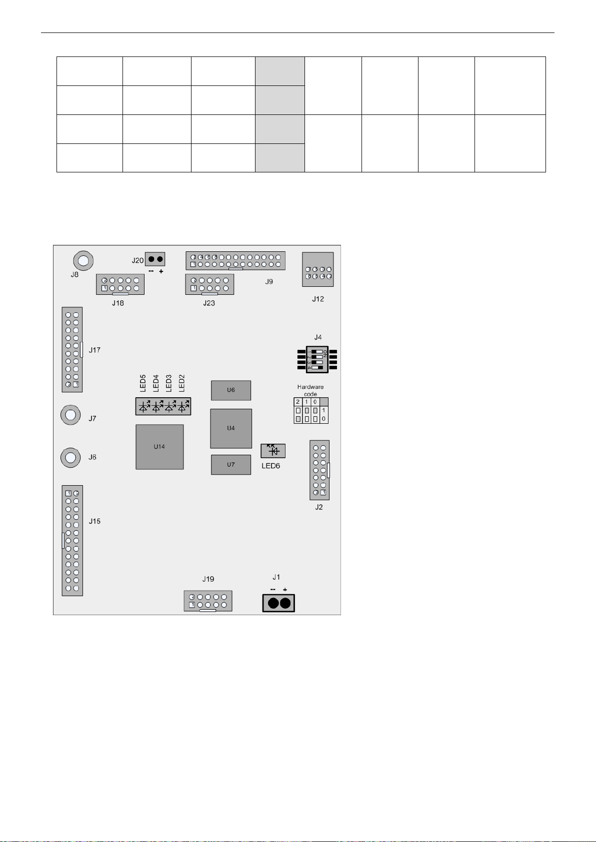
Figure 3-16 Baseband Board I nt er fac e and I ndicator
See Figure 3-16, Th e int erfaces and indicators of banseband are as follows:
J1 is the 13.2V(+/-20%) DC input interface of the whole banseband mainboard, and the polarity
should be noted. The input circuit includes isolating magnetic inductor (L12) and chip insurance resistor
(F1).
J2 is the JTAG adjustment interface of main processor, and it is used for program simulation
adjustment.
J4 is the switch for boot mode. See“3.3.5Boot Mode” for details.
J6、J7 are 12.8MHz clock and SMA offered by main board to other p art s. The two signals are the same
17
Page 22
TR850 Service Manual
and either one of them can be selected.
J8 is the interface and SMA of GPS interface, and it supp orts active antenna with 3.3V feed output.
J9 is the ACCY external interface provided by baseband, and it is used for function expansion or test.
It includes the input and output of loc al speech, external PTT, and pr ogramm able exp ans ion IO. It provides
12V/1A DC output.
J15 is the interface of Rx board, including digital IF, SPI interface signal, 12C interface sig nal for storing
data of test and adjust m e nt, etc.
J17 is the interface of Tx board, includ ing two point modulation si gnal, SPI int erface of Tx circu it PLL, Tx
control signal, etc.
J18 is the control interface of RF power amplifier, including SWR , TEMP_DET, POWER_CONTROL,
TX_ENABLE, etc.
J19 is the interface of LED status display board.
J20 is the 12VDC fan interface.The fan will be switched on when the r adio tr ansmits or the temperature
goes beyond the set range.
J23 is the serial port UART2.
LED2、LED3、LED4、LED5 indicates program operation status.
LED6 indicates CPU power.
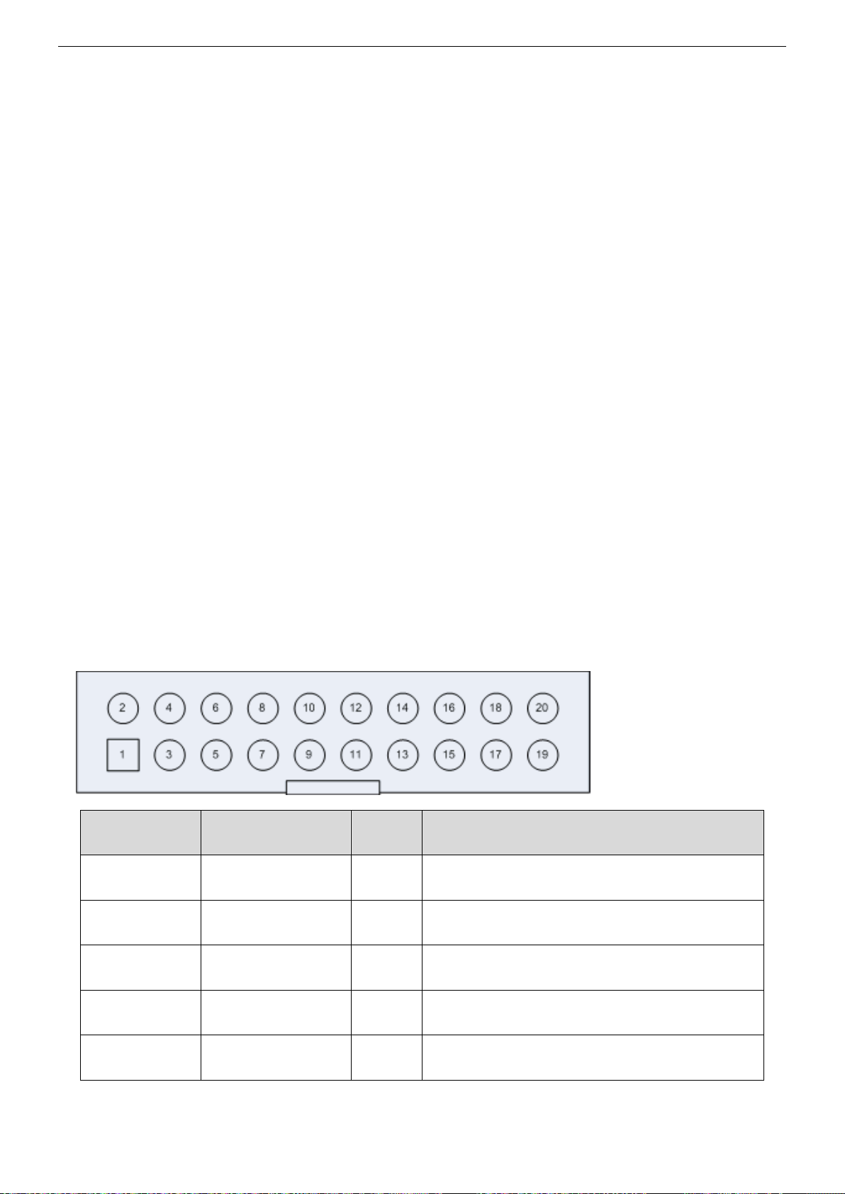
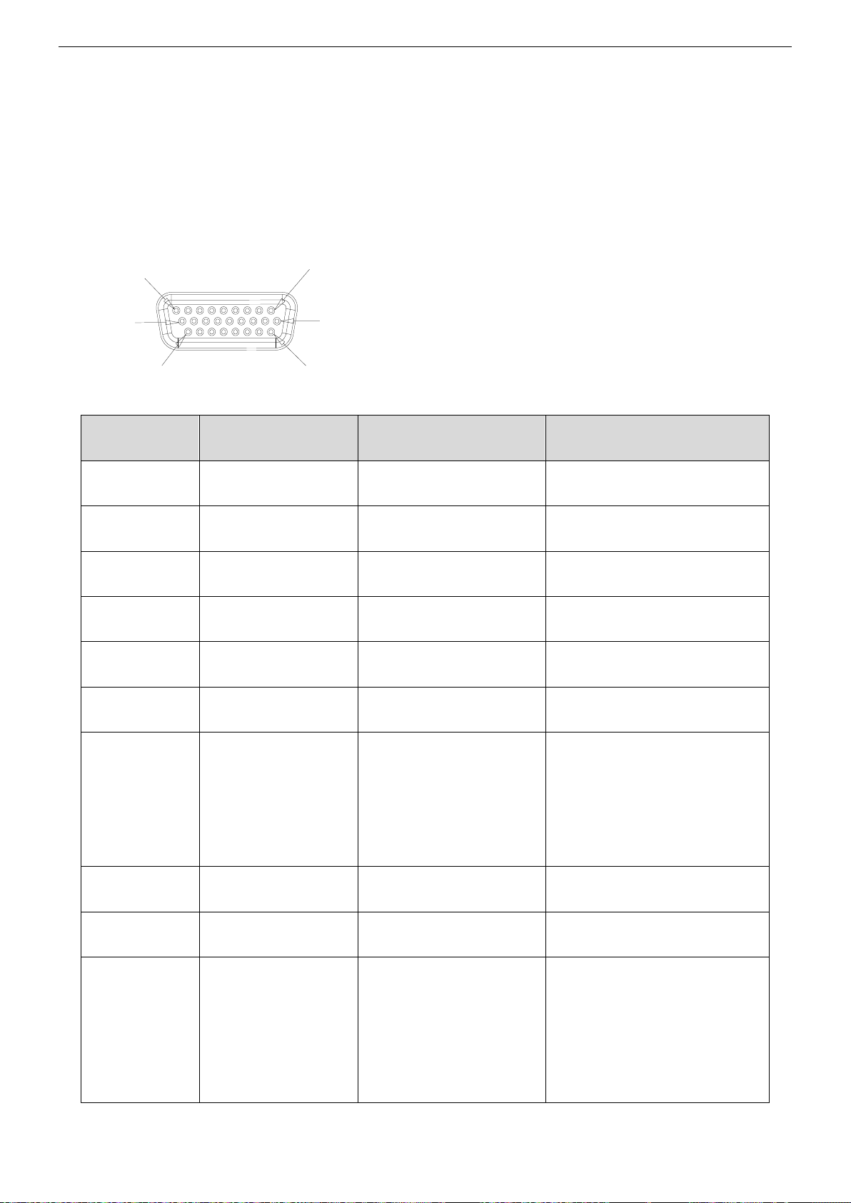
3.3.8. Tx Unit Interface Definition (J17)
Figure 3-17 Tx Unit Interface Definitio n
Ter minal NO. Terminal Name I/O Function
1 GND - Ground
2 MOD1 O TX Modulate signal output1
3 GND - Ground
4 MOD2 O TX Modulate signal output2
5 GND - Ground
18
Page 23
TR850 Service Manual
6 NC - -
7 GND - Ground
8 NC - -
9 TX_LD O PLL locked indicate,active high
10 TX_VCO_SEL O Select VCO band
11 SPI_CLK O SPI clk
12 GND - Ground
13 VCCTX O Open TX Power,active high
14 GND - Ground
15 SPI_MOSI I/O SPI data
16 GND - Ground
17 PLL_CS O PLL chip selected,,active low
18 TX_ENABLE O Enable TX PLL,,ac t iv e high
19 VCC O 13.2V output
20 VCC O 13.2V output
3.3.9. RF Power Amplifier Module Interface (J18)
Figure 3-18 RF Power Amplifier Module Interface
19
Page 24
TR850 Service Manual
Resets AD9864 SSI and DecimatorCounters;
Ter minal NO. Terminal Name I/O Function
1 POWER_CTRL O PO WER contr ol o utput
2 GND - Ground
3 POWER_SWITCH O POWER switch,active high
4 NC - -
5 TX_ENABLE O Power modul e enbale,active high
6 NC - -
7 SWR_R I Power SWR_R detector
8 TEMP_DET I Power tempreture detect or
9 SWR_T I Power SWR_T dete ct or
10 NC - -
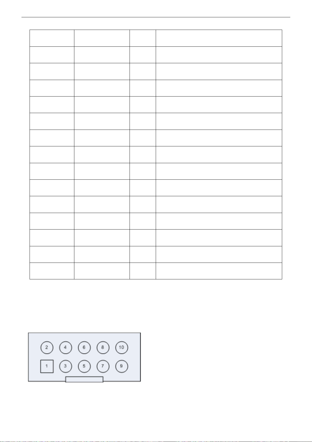
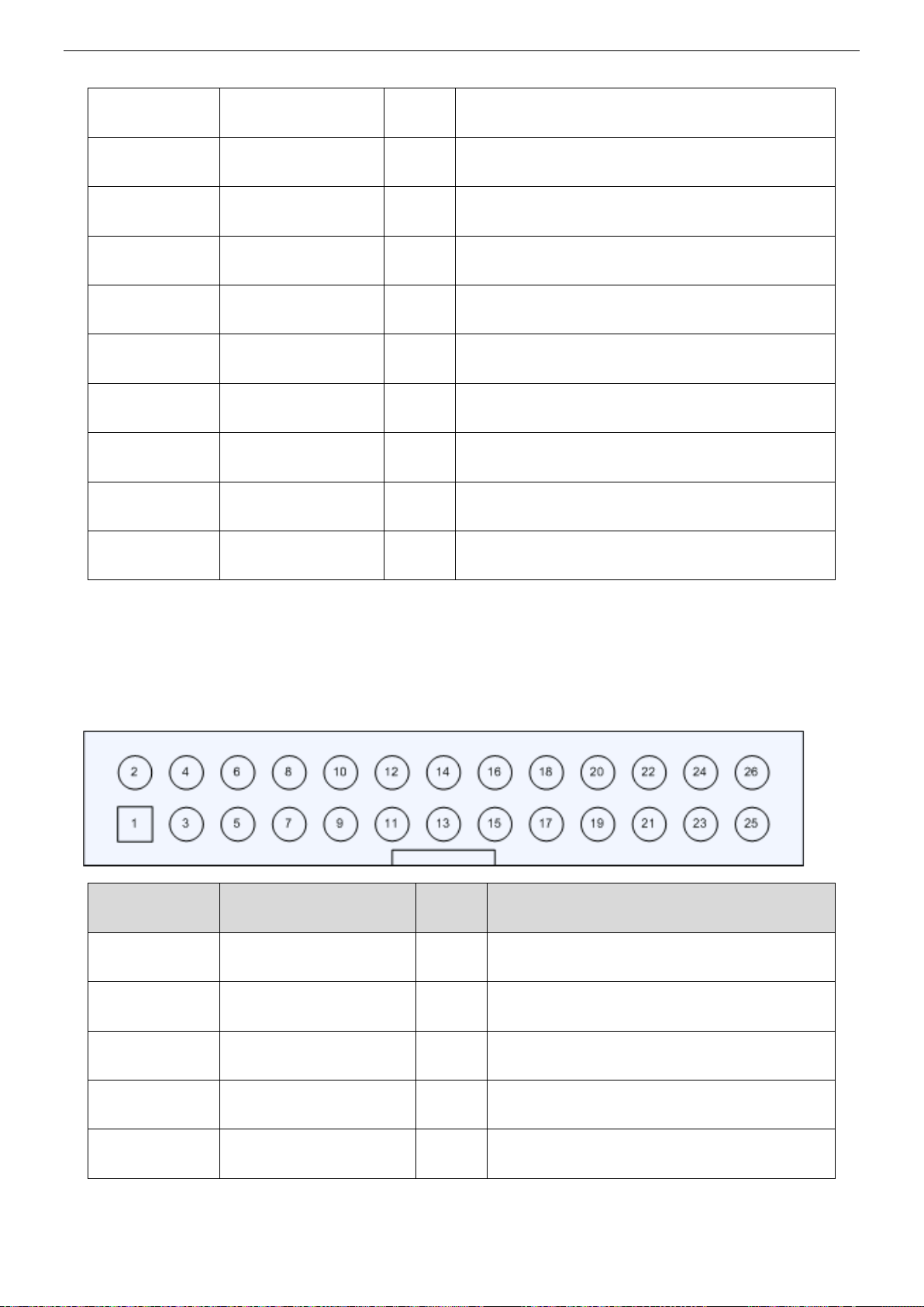
3.3.10. Rx Unit Interface Definition (J15)
Figure 3-19 Rx Unit Interface
Ter minal NO. Terminal Name I/O Function
1 SYNCB O
2 SPI_MISO I Data for AD9 864 SPI
3 AD9864_DATAOUT I Data for AD9864 SSI
4 AD9864_CLK I Clock for AD9864 SSI
Active Low
20
Page 25

TR850 Service Manual
5 AD9864_FS I Frame synchronous for AD9864 SSI
6 SPI_CLK O Clock for AD9864 SPI
7 SPI_MOSI O Data for A D9864 SPI
8 AD9864_SPI_CS O Enable for AD9864 SPI
9 RX_VCO_CTRL O VCO tunner
10 RX_PLL_CS O PLL chip selected, active low
11 I2C_SDA I/O EEPROM data
12 I2C_SCL O EEPROM clock
13 RX_LD O PLL locked ind icate,active high
14 GND - Ground
15 RX_BPF_CTRL O Output for RX BPF filter tunner
16 NC - -
17 VCCR8X O Open RX Power,active high
18 GND - Ground
19 RX_VCO_SEL O select VCO band
20 NC - -
21 I2C_A0 O EEPROM address
22 NC - -
23 GND - Ground
24 NC - -
25 VCC O 13.2V output
26 VCC O 13.2V output
21
Page 26
TR850 Service Manual
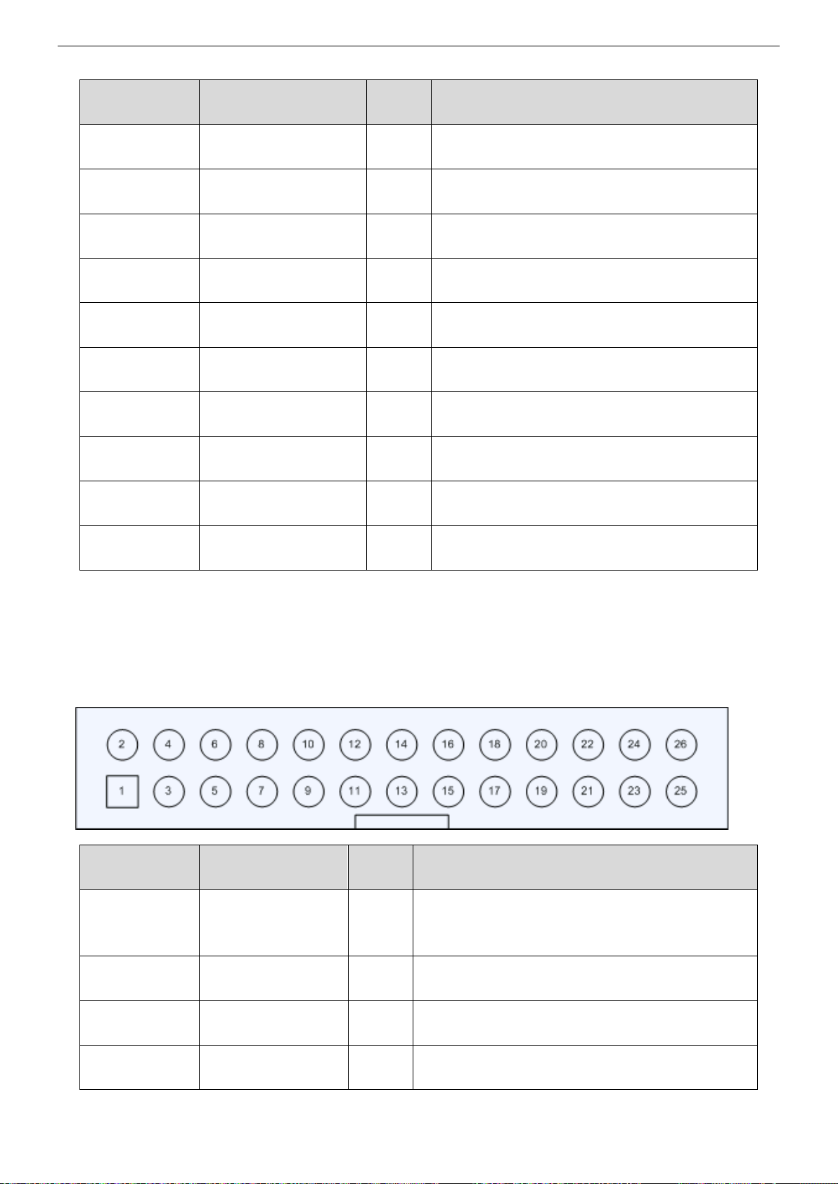
3.3.11. Front Panel Interface Definition (J19)
Figure 3-20 Front PanelInter fac e Definition
Terminal NO. T erminal Name I/O Function
1 3V3 - 3.3V
2 GND - Ground
3 LED0 O TX_A slot indicate, active high
4 LED4 O REPEATER mode indicate,active high
5 LED1 O RX_A slot indicate, act ive high
6 LED5 O ANALOG mode indicate,active high
7 LED2 O TX_B slot indicate,active high
8 LED6 O DIGITAL mode indicate,active high
9 LED3 O RX_B slot indicate,active high
10 LED7 O ALARM indicate,active high
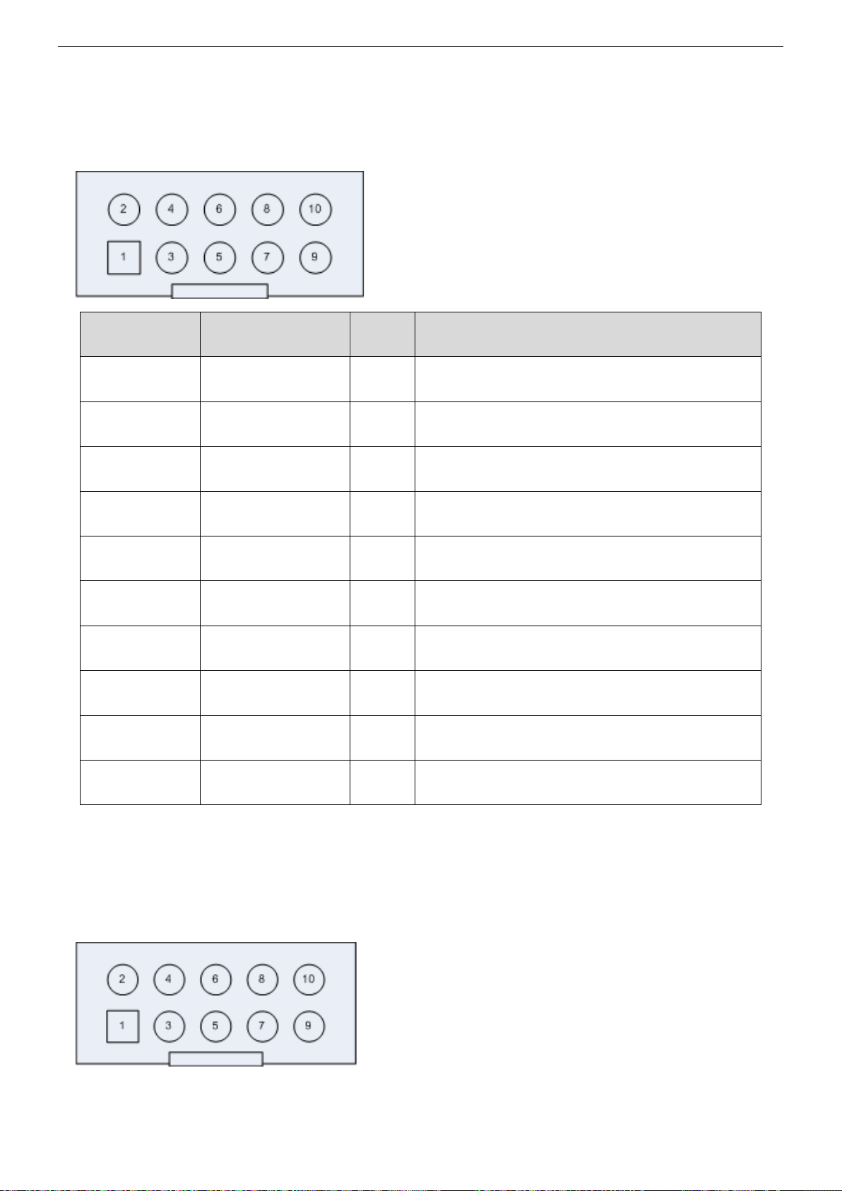
3.3.12. Serial Port Definition (J23)
Figure 3-21 Serial Port Definition
22
Page 27
TR850 Service Manual
Ter minal NO. Terminal Name I/O Function
1 NC - -
2 NC - -
3 TXOUT O RS232 TX output
4 NC - -
5 RXIN I RS232 RX input
6 NC - -
7 NC - -
8 NC - -
9 GND - Ground
10 NC - -
3.3.13. JTAG Simulator Interface Definition (J2)
Figure 3-22 JTAG Simulator Interface Definit ion
Ter minal NO. Terminal Name I/O Function
1 TMS - TMS
2 TRST - TRST
3 - - -
4 - - -
23
Page 28
TR850 Service Manual
5 - - -
6 NULL - NULL
7 - - -
8 - - -
9 - - -
10 - - -
11 - - -
12 - - -
13 - - -
14 - - -
3.3.14. External Interface Definition (J9)
Figure 3-23 Externa Interface D ef in it io n
Ter minal NO. Terminal Name I/O Function
1 USB_D+ I/O Reserved
2 USB_D- I/O Reserved
3 V_BUS O Reserved
4 USB_GND - Ground
5 ACC_ID2 I Reserved
24
Page 29
TR850 Service Manual
6 ACC_ID1 I Reserved
7 EXT_SWB+ O Power 13.2VDC switched out put
8 POWER_GND - Ground
9 EXT_SPK- O Annalog output speaker-
10 EXT_SPK+ O Analog output speaker+
11 TX_AUDIO I Analog audio input
12 AUDIO_GND - Ground
13 AUX_AUDIO_OUT1 O Reserved
14 RX_AUDIO I Reserved
15 AUX_AUDIO_OUT2 O Reserved
16 GND - Ground
17 PRGM_IO_1 I PTT input,high active
18 GND - Ground
19 PRGM_IO_2 I/O Reserved
20 PRGM_IO_6 I/O Reserved
21 PRGM_IO_3 I/O Reserved
22 PRGM_IO_7 O Output high level(2.8V)
23 PRGM_IO_4 I/O Reserved
24 PRGM_IO_8 I/O Reserved
25 PRGM_IO_5 I/O Reserved
26 PRGM_IO_9 I/O Reserved
25
Page 30
TR850 Service Manual
10
18
19
26
9
1
3.3.15. Case External Interface Definition
Extended interface (J9) of base ban d is conn ected t o access ory board by a flat gray cable, t hen connect ed
to the ACCY connector at the rear of repeater after conversion through accessory board. The ACCY
connector is as following Figure 3-24.
Figure 3-24 ACCY Interface
Ter minal NO. T erminal Name I/O Function
1 Ext_SWB+ +13V Output +13.8V output(Imax<1A)
2 GND Ground Ground
3 USB_D+ Reserved
4 USB_D- Reserved
5 USB_VBUS Reserved
6 USB_GND USB Ground
External PTT Signal
input, High level
7 Program_IN_1 (PTT)
8 Ext_Spk- External Speaker output 8 Ω /16Ω, 0.8W Max
active .when connected
with Pin20, enter
transmission mode
Digital Input:
(2.5V<VIH<3.3V,0V<VIL<0.4V)
9 Ext_Spk+ External Spea ker out put 8 Ω /16Ω, 0.8W Max
Accessory ID input Line 2
Control signal, when
10 ACC_MAP_ID_2
connected with Pin20,
mode of analog RX
performance testing
26
Digital Input:
(2.5V<VIH<5V,0V<VIL<0.4V)
Page 31

TR850 Service Manual
Accessory ID input Line 1
11 ACC_MAP_ID_1
12
Squelch
(Program_IO_6)
13 RXD
14 TXD
Control signal, when
connected with Pin20, the
IP address will be set t o
the default address:
192.168.1.100.
Digital Input. High lev el
will enable opening
squelch when connecte d
with Pin20.
Output.
Receive signal from
repeater to PC
Input.
Transmit signal from PC
to repeater
Digital Input:
(2.5V<VIH<5V,0V<VIL<0.4V)
Digital Input
(2.5V<VIH<5V,0V<VIL<0.4V)
RS232 Level:
-3V ~ -15V
+3V ~ +15V
RS232 Level:
-3V ~ -15V
+3V ~ +15V
15 GND Ground -
16 Rx_Audio NULL -
17 Audio_Ground Ground -
18 Tx_Audio
External Audio signal
input
19 GND Ground -
Output high level, used
with Pin7 (PTT functi on) ,
20 Program_IO_7
Pin10 (analog Rx
function) and Pin11 (IP
address reset function)
and pin23(open squelch)
21
Program_IO_4
(Emergency)
NULL -
Analog input:0V<VIL<0.5V
Digital Output
2.5V<VOH<3.3V
22 Program_IO_8 NULL -
27
Page 32

23 Program_IN_5
TR850 Service Manual
Digital Input
High level active Opening
squelch when connected
with Pin20
Digital Input:
(2.5V<VIH<5V,0V<VIL<0.4V)
24
Program_Out_9
(Ext_Alarm)
Reserved -
25 Aux_Audio_Out1 NULL -
26 Aux_Audio_Out2 NULL -
4. Function and Parameter Setting
4.1. Conventional Functions
Conventional DMR functions:
Supports DMR dual slot mode
Supports DMR private call , group calla and all call transfer
Supports short Message, status mes sage transfer
Supports end to end voice and dat a encryption
Supports GPS
Supports interruption and monitor function
Supports stun, activation, kill signal ing tr ansfer
Supports IP connection
Supports S tandard AIS Interface
Support Analo g and Digital Mode
Supports Pseudo Trunkin g
4.2. Parameter Setting
Repeater is set with default par ameters when l eaving t he factory. Parameters such as operatio n frequency,
channel paramenters, scan and encryption may be changed according to different requirement by
users.Therefore, Kirisun specially designed programmable software CPSp, which is interface-friendly,
easy to operate and display-friendly, to realize the setting for repeater function para meters.
28
Page 33

TR850 Service Manual
4.2.1. Parameters setting
Parameter settings steps are as follows
Step 1. Install the right versio n of the CPSp user programming software.
Step 2. Using RJ45 ethernet cable to connect the repeater with Ethernet port of computer through
HUB/switchboard.
Step 3. Make sure the repeater is power ed on.
Step 4. Operate CPSp user programming soft w ar e f or t he settings of related parameters.
The user can read parameter configuration through CPSp user programming software.
4.2.2. Install CPSp user programming software
Installation steps of CPSp user programming software:
Step 1. Double click the installation file of CPSp user programming software, and the interface below will
pop up.
Step 2. Click “Next” and enter the next interface.
Step 3. (Option) Click browse and select the inst allation route.
This step can be skipped if using t he default route.
29
Page 34

TR850 Service Manual
Step 4. Select the language you wish to install.
Step 5. Click “Next” and install the software.
30
Page 35

TR850 Service Manual
Step 6. Click “Finish” to finish the installation.
Step 7. Please double click the CPSp user programming so ftwar e to operate after acquiring authorization.
See the figure below.
31
Page 36

TR850 Service Manual
Please refer to the help file in the CPSp user programming software for more details.
Note:
1. Errors of parameter configuration may cause malfunctions, but normally you can rewrite the
correct parameter configuration.
2. Before parameter configuration modification, we strongly recommend a backup for the current
parameters to make sure that the parameters can be restored after an error occurs.
5. Assembly and Disassembly Instruction
5.1. Duplexer Assembly
Step 1. Loosen the four screws on the top and the three screws on both sides of the top shell, and
remove the shell upwards.
32
Page 37

TR850 Service Manual
Step 2. Loosen the two screws on the duplex baffle, and remove the duplex baf fle.
Step 3. Loosen the two screws which fix the duplex bracket till the bracket can be slided in the track
groove.
33
Page 38

TR850 Service Manual
Step 4. Use screws to fix the rear part of the duplex on the bracket, and push the duplex into the box till
the duplex can be properly fit into the three corresponding holes in t he box before fixing the screws on
the duplex bracket.
5.2. Disassembly Instruction
The repeater is divided into the two parts below:
Area allowed for users to assemble and disasse mble: I nternal area of the t op shell. Us ers can assemble
duplex.
34
Page 39

TR850 Service Manual
Area allowed for dealers with maint enance permit to assemble and disassemble: Internal area of the top
shell and internal area of t he lower shell.
35
Page 40

5.3. Exploded View
1
2
3
4
5
6
7
10
11
13
14
12
15
16
17 18
19
20
21
8
9
22
2
20
23
24
25
26
27
28
29
30
31
32
33
34
13
35
36
29
40
37
38
39
41
42
43
44
45
46
47
48
49
50
57
58
30
59
28
27
38
52
41
51
53
54
55
56
9
13
TR850 Service Manual
No. Part No. Description Quantity
1 7WOZ-4100-01A Top panel, 1mm color zinc-plated board, dusting, with
decorative stripes.
1
2 7SMF-030050M-SZC
T-N1
3 7SAF-040080M-SZH
T-N
M3*5 cross sunk machine screws. Mat er ial: stainless
steel, φ3mm*5mm cross sunk machine thread,
metric coarse thread, blac k nickel-plated
M4*8 cross thick head combination machine screw
Material: hardened iron,w i th flat spacer and spring
36
24
6
Page 41

TR850 Service Manual
spacer, pb-free.
4 7MBF-4027-02A-X0 DR550 50W duplex bracket, zinc-plated boar d, 1.5mm
1
thick, color zinc-plated, pb-free.
5 7NHF-040008030-N1 M4*3 hexagonal nut mate rial: iron, internal diameter
6
M4mm, maximum external diameter 8mm, 3mm thick,
hexagonal nickel-plated nut.
6 Duplex, self-purchase
7 0ADY-4071-D STR-U pow er module, SP-320-12, 12V, 320W, ROHS,
10
1
with fan.
8 7SAF-030050M-SZY
B-Z1
M3*5 cross round flat head co mb ination machine
screw. Material: hardeded iron, Φ3mm*5mm with flat
10
spacer and spring spacer, pb-free
9 3CB1-151007-B Cable tie holder NYLON 66, 15X10X7, pb-free 10
10 7SAF-040060M-SZH
M4*6 cross thick head combination machine screw. 4
T-N
11 7WOZ-4071-03A Intermediate board 2, 1mm thick color zinc-plated
1
board.
12 6SS2-4071-HWA STR-U repeater power board jacking 1
13 7SAF-030080M-SZY
B-Z1
M3*8 cross round flat head co mb ination machine
screw. Material: hardeded iron, Φ3mm*8mm, with flat
28
spacer and spring spacer, pb-free.
14 7NHC-055070306-LJ M3*7+6 Hexagonal Copper Cylinder 19
15 6SS2-4071-HBA
STR-U/V Repeater Base Band Board Jack in g 1
16 7MHF-4100-01A-W TR850 DMR front panel, 5mm thick aluminum
1
material, oxidized black, l aser car ving, with copper
cylinder
17 7MHP-4071-01-W0 Handle, aluminum, oxidized black 2
18 7MBP-4100-01A-W TR850 lens 2mmthick, PMMA, transparent, screen
1
printing
37
Page 42

TR850 Service Manual
19 3SB3-YB-S1-Q AC power switch. 1
20 7GCR-4071-01A-W0 Repeater foot pad (4 pieces) silica gel, with screws (4
1
pieces)
21 7GCJ-S4071-J STR-U lens double side ta pe, NITTO 57120B double
1
side tape, pb-free
22 7WOZ-4100-02A Down panel, 1mm thick color zinc-plated boar d,
1
dusting.
23 6SS2-4071-HFB STR-U/V repeater front panel jacking 1
24 7SMF-030050M-SZY
B-N
M3*5 cross round flat head machine screw
Material: hardened iron, Φ3mm*5mm cross round
5
flat head nickel-plated machine thread, metric coars e
thread
25 7WOZ-4071-02A Intermediat e boar dm 1, 2mm thick color zinc-plated
1
board, rivet screw column
26 7SMF-030250M-SZC
T-N1
27 7SMF-030180M-SZC
T-N1
28 7MHL-4071-03A-W STR-U receive module aluminium shield down case
M3*25 cross sunk machine screw
metric coarse thread, whit e nickel-plated
M3*18 cross sunk machine screw
metric coarse thread, whit e nickel-plated
8
16
1
Aluminum
29 7SMF-030060M-SZY
B-N
M3*6 cross round flat head machine screw
Material: hardeded iron,Φ3mm*6mm metr i c c oar se
61
thread
30 6SS2-4067-HRB DR650-02receiving board jacking 1
31 7MHL-4071-02A-W STR-U receive module aluminium shield down case
1
32 3CB1-004071-A
Aluminum
STR-U Power Amplifier Board fixed socket processed
with aluminum alloy
38
1
Page 43

TR850 Service Manual
33 7SAF-030050M-SZY
B-Z1
M3*5 cross round flat head machine screw
Material: hardeded iron, with flat spacer and spring
10
spacer, pb-free.
34 7MBC-4071-01A-W
STR-U power amplifier module big shield cover ,
stainless steel,
0.5mm thick
1
35 7MMC-1943-01A-N PT8200 power module shield cover; pb-free 1
36 1MR3-RA55H4047M UHF RF amplifier IC 8200-02, DR550H STU 1
37 6SS2-4071-HPC STR-U power amplifier jacking (130722) 1
38 7SMF-030060M-SZC
T-N1
M3*6 cross sunk machine screw
Material: hardened iron, φ3mm*6mm cross sunk
8
machine thread, metric co ar se t hr ead, black
nickel-plated.
39 7MHL-4071-01A-W STR-U radiator; processed with aluminum alloy 1
40 3CR7-N-KKF1 RF connector 1
41 7SMF-030100M-SZC
T-N1
M3*10 cross sunk machine screw
Material: hardened iron, φ3mm*10mm cross sunk
12
machine thread, metric co ar se t hr ead, black
nickel-plated.
42 4MF7-DFB602512HM Fan DFB602512HM, Specification: 12V/0.3A,
1
60X60X25mm
43 7MHF-4027-02A-Z DR550 Fan-fixing bracket, zinc-plated board,
1
0.8mm thick , black dusting on surface
44 7STF-050120A-SZHT
-N
45 7WOZ-4100-04A Duplex baffle 1mm, thick color zinc-plated board,
M5*12 cross thick head self-t apping screws.
Hardened iron
4
1
dusting
46 7WOZ-4100-03A Rear pan el (part no. cancelled) 1.5mm thick color
1
zinc-plated board, dusting
47 7SAF-040100M-SZLJ M4*10 Cross external hexagonal combination 4
39
Page 44

TR850 Service Manual
-Z1 machine screw. Material: har dened iron
48 7MHS-4027-06A-W M4*8 grounding screw; stainless steel, M4.0*8 1
49 3CR7-SMA-160 RF coaxial line-1 SMA-C-KY1.5-1 to SMA-C-JW1.5,
1
type: RG141A/U, line length 160mm
50 3CR7-BNC-440 BNCcoaxial line SMA-C-J1.5 to BNC(rectangular
1
flange plate 24*24),RG141A/U, line length: 440mm
51 3CP3-YB-B2-Q1 Power socket, 2.5A T 20mm HRC 250V type 1
52 3WPC-WS20K2Z Two core aviation socket, WS20K2Z 1
53 7NHF-030062025-Z1 M3*2.5 hexagonal nut. Mat erial: iron, inter nal diamet er
10
M3mm, maximum external diameter 6.2mm, 2.5mm
thick, hexagonal and zinc-plated, metric coarse
thread.
54 6SS2-4071-HL1A STR-U repeater accessory board plug-in material 1
55 3WPC-812028-A STR-U Network port connecting wire 8pin, wire length
1
120mm, 28AWG, with network port and crystal head.
56 7WOZ-4100-05A Network port ba ffle, 1mm thick color zinc-plated board 1
57 7MHL-4071-04A-W STR-U Tx module aluminum alloy shield bottom cover 1
58 6SS2-4067-HTB DR650-02 Tx module jacking DR650-02 Tx module
1
jacking, pb-free
59 7MHL-4071-05A-WA STR-U Tx module aluminum al loy s hie ld up cover 1
40
Page 45

5.4. Connection
1
2
3
4
6
8 7
5
9
10
13
14
15
16
18
17
11
12
TR850 Service Manual
41
Page 46

TR850 Service Manual
23
22
+ -
+ -+-
24
28 29
25
26
27
31
30
32
34
35
33
Part no. Description Connect mode
Power connecting line-1 3 Pin, 135mm long, wire
3WPD-S4071-A
size16AWG. one e nd with cold-press sockets
terminal, one end round term inal.
6—31
3WPD-S4071-B
Power connecting line-2, 2Pin,red length 950mm
long, black wire 415mm, wire size 12AWG, both
ends with two round terminals.
42
28—30
Page 47

TR850 Service Manual
3WPD-S4071-C
3WPD-S4071-D
3WPD-S4071-E
3WPD-S4071-F
3CR7-SMA-160
3CR7-SMA-110A
Power connecting line -3 2Pin, 665mm lon g, wire
size 12AWG
Power connecting line -4 2Pin, 315mm lon g, wire
size 12AWG. One end with two round terminals, an d
the other a base.
Power connecting line-5 2 pin, 575mm long, wire size
18AWG, 3.96 interval, with soc ket and round
terminal.
Power connecting line-6 2pin, wire lengt h 550mm,
wire size 20AWG, inter val 2.54, with socket and
cold-press sockets t erminal
RF coaxial wire-1 SMA-C-KY1.5-1 to SMA-C-JW1.5,
wire type: RG141A/U, wire length 160mm
RF coaxial wire -2 SMA-C-J1.5 to
SMA-C-JW1.5,wire type: RG141A/U, wire length
110mm
7—29
24—35
18—25
2—26
3—13
15—21
3CR7-BNC-440
3WPC-812028-A
3WPT-P26050PH25420P
3WPT-P26050PH25426P
3WPD-S4071-G
3CR7-SMA-350
BNC coaxial wire, SMA-C-J1.5 to BNC(rectangular
flange plate 24*24), RG141A/U, wire length: 440mm
STR-U internet port connecting wire 8pin, wire length
120mm, 28AWG, with internet port and crystal head,
With dual-plugged flat cable AWG26#, 2.54 interval,
wire length 50mm, 20P socket, dual-headed soc ket
With dual-plugged flat cable AWG26#, 2.54 interval,
double flat cable, wire len gth 50mm, 26Psocket,
dual-headed socket
Power connecting line-7 2pin, w ire l ength 350mm,
wire size 20AWG, 2.54 interval, with socket and
cold-press sockets t er m in al
RF coaxial wire -3 SMA-C-JW1.5 to SMA-C-JW1.5,
wire type:RG141A/U, wier length 350mm
8—20
5—9
14—23
16—19
2—27
22—34
3WPT-P26155PH25426P
With three-plugged flat cable, AWG26#, 2.54
interval, three flat cable, 155mm long
43
4—10
Page 48

TR850 Service Manual
3WPT-P26350PH25410P
3WPT-P26080PH25410P
3WPD-160140-1PIN
Fan wire Come with fan
With dual-plugged flat cable, AWG26#, 2.54 interval,
double flat cable, wire len gth 350mm, 10P socket.
With dual-plugged flat cab le, AWG26#, 2.54
interval, double flat cab le, wire length 80mm, 10P
socket, double-headed s ocket.
Connected to ground wire 1Pin, blue wire, 140mm
length,wire siz e ,:16AWG.; two ends with r ound
terminal
1—12
17—33
31(ground
terminal)—
machine case
11—32
6. Adjustment
During maintenance, the repeater may needs some testing and modulation for technical index after
changing the components.
6.1. Preparation
Please prepare the tools and equipment before testing the DMR repeat er:
Integrated tester
PC and CPSp software
AEROFLEX 3920
Spectrum analyzer FSU
Antenna interface converter
Universal interface
6.2. Method of Modulation and Test
6.2.1. Local Oscillator Adjustment
Subject Test Point Test Procedure Standard
12.8M
Clock
base band
board J6
1. Enter test mode “12.8M Cl ock”.
2. Set HP8921 to TX mode; connect the reference
frequency port to HP8921 RF high power input
port.
3. Enter computer modulation mode.
44
≤±1Hz
Page 49

Rx
localoscilla
tor power
Tx central
frequency
&power
Rx board
test point
TP3005
Tx module
J200
TR850 Service Manual
4. Adjust to 12.8MHz±1Hz.
1. Enter test mode “Receiver BPF”.
2. Set HP8921 to TX mode.
3. Connect the TP3005 test poit on the RX board
to HP8921RF high power input por t .
4. Check the frequency: (Rx frequency
-51.65MHz)±100Hz; output power >10dBm.
1. Enter test mode “Low Freq.M od Deviatio n”.
2. Set HP8921 to TX mode.
3. Connect Tx module RF output to HP8921 RF
high power input port.
4. 4. Adjust to :±100Hz, Chec k: out put pow er>
15dBm.
1. Turn on the repeater.
Frequnency
tolerance≤±
200Hz
Output power>
10dBm
Frequency
tolerance≤±
200Hz
Output power>
15dBm
2. Set HP8921 to TX mode.
Tx lock
voltage
testing
Rx lock
voltage
test
Tx board
TP100
Rx board
TP100
3. Connect TX por t t o HP8921 RF high power input
port.
4. Enter computer modulat io n mo de.
5. Click Tx low pow er tes t po int s to test lock v olt ag e
1. Turn on the repeater.
2. Set HP8921 to TXmode.
3. Connect TX por t t o HP8921 RF high power input
port
4. Enter computer modulat io n mo de.
5. Click Rx sensitivity test point s to t est lock volt ag e
0.5V≤CV voltage
≤4.5V
0.5V≤CV voltage
≤4.5V
6.2.2. Tx Adjustment
Subject Modulation Procedure Standard
Tx high
power
Tx low
power
1. Enter pc tuning mode.
2. Enter modulation mode”High Power”.
3. Adjust PC software val ue; observe power value on the
integrated tester.
4. Adjust to test power: 40±2W.
5. Modulate the frequency one by one.
1. Enter computer modulation mode.
2. Enter modulation mode “Low Power”.
3. Adjust PC software valu e; obser ve power value on the
45
40±5W
20W±1.5db
Page 50

Low
frequency
modulation
frequency
deviation
High
frequency
modulation
frequency
deviation
TR850 Service Manual
integrated tester.
4. Adjust to test power: 20W.
5. Modulate the frequency one by one.
1. Enter computer modulat io n mo de.
2. Click frequency F1 to F6.
3. When AF Freq is 0.1kHz, observe FM Deviation on the
integrated tester, and modulate PC soft w ar e value.
4. Adjust FM Deviation to 5.0±0.05kHz.
5. Click “ok” to save.
1. Enter computer modulat io n mo de.
2. Click Frequency F1 to F6.
3. When AF Freq is 6.0 kHz, observe FM Deviation on the
integrated tester, and modulate PC software value.
4. modulate FM Deviationto5.0±0.05kHz.
5. Click “ok” to save.
4.95kHz-5.05kHz
4.95kHz-5.05kHz
4FSK EER
test
Maximum
audio
frequency
deviation
test.
QT/DQT
frequency
deviation
and wave
form test.
1. Enter computer modulat io n mo de.
2. Modulate PC software value to make repe at er transmit
O.153.
3. Check 4FSK EER≤5%.
4. Modulate frequenciesone by one.
5. Observe FSK EER value on the integrated test er.
6. Check 4FSK EER≤5%.
1. Connect the audio input wire to repeater.
2. Output audio signal 1KHz RMS 120 mV to repeater and make it
transmit.
3. The audio frequency deviation should be: N: 2000±100Hz,
W:4000±100Hz.
4. Test frequencies one by one.
1. Observe frequency deviation of QT.
2. Observe frequency deviation and wave form of DQT.
FSK EER≤5%
N: 2000±200Hz
W: 4000±400Hz
N: 350±150Hz
W: 750±250Hz
Modulationdi
stortion
Observe distortion for m v alue.
Tx SNR Observe SNR form value
<3%
W: >45dB
N: >40dB
46
Page 51

TR850 Service Manual
Analog&digit
al ACP
Spurious
emission
Observe ACP display value.
Observe spectrum analyzer display value.
6.2.3. Rx Adjustment
Modulation
Subject
Modulation Procedure Standard
W: <-70dB
N: <-60dB
<1GHz: <
-36dBm
>1GHz: <
-30dBm
Rx Sensitivity
Narrow band
squelch level
9 on
Narrow band
squelch level
9 off
1. Enter computer modulation mode.
2. Enter modulation mode ”Receiver BPF”, and clic k the six
frequencies one by one.
3. Make SINA>12dB.
4. Set the four Rx frequencies as -25.825MHz(*1、*2、*3、*4),
and signal strength as -40dBm; the SINA should be<7dB.
1. Enter computer modulat io n mo de
2. Set the channel to the current modulation frequency.
3. Enter modulation mode “SQL9 Open (N)”, and click “start”,
and change to the next frequen cy after the value is stable.
4. Modualte the frequency of nar r ow band and wide band in
turn.
1. Enter computer modulation mode.
2. Set the channel to the current modulation mode.
3. Enter the modulation mode ”SQL9 Close(N)”, and click
“start”, and change to the next frequency after the value is
stable.
-
-
-
4. Modulate the frequency of narrow band and wide band in
turn.
47
Page 52

Narrow band
squelch level
1 on
Narrow band
squelch level
1 off
TR850 Service Manual
1. Enter computer modulation.
2. Set the channel to the current modulation mode.
3. Enter the modulation mode “SQL1 Open(N)”, and click
“start”, and change to the next frequency after the value is
stable.
4. Modulate the frequency of narrow band and wide band in
turn.
1. Enter computer modulation.
2. Set the channel to the current modulation mode.
3. Enter the modulation mode “SQL1 Close(N)”, and click
“start”, and change to the next frequency after the value is
stable.
4. Modulate the frequency of narrow band and wide band in
turn.
1. Enter computer modulat io n mo de.
-
-
Wide band
squelch level
9 on
Wide band
squelch level
9 off
Wide band
squelch level
1 on
2. Set the channel to the curr ent mo dulation mode.
3. Enter the modulation mode “SQL9 Open( W)” , and click
“start”, and change to the next frequency after the value is
stable.
4. Modulate the frequency of nar row band and wide band in
turn.
1. Enter computer modulation mdoe.
2. Set the channel to the current modulation mode,
3. Enter modulation mode “SQL9 Close(W)”, and click “start”,
and change to the next frequen cy after the value is stable.
4.Modulate the frequency of narrow band and wide band in
turn.
1. Enter the computer modulation mode.
2. Set the channel to the current modulation mode.
3. Enter the modulation mode “SQL1 Close(N)”, and click
“start”, and change to the next frequency after the value is
stable.
-
-
-
Wide band
squelch level
1 off
4. Modulate the frequency of nar row band and wide band in
turn.
1. Enter the the computer modulation mode.
2. Set the channel to the current modulation mode,
3. Enter the modulation mode “SQL1 Close(N)”, and click
“start”, and change to the next frequency after the value is
stable.
4. Modulate the frequency of nar row band and wide band in
turn.
48
-
Page 53

TR850 Service Manual
Rx distortion Observe the distorti on value,
Rx SNR Observe SNR value
CTCSS/CDC
SS
BER Test
-
1. Set the output range of 3920 as -118dBm.
2. Enter BER test mode.
3. Click “Start”, and observe BER.
<3%
W: >45dB
N: >40dB
Can transmit
EER≤5%
7. Main Technical Functions and Specifications
General Specificatio n
Frequency Range
UHF: 400-470MHz VHF:136-174MHz
Channel Capaci t y
Channel Spacing
Weight
Dimension(H*B*D)
Environment Index
Operating
Temperature
Storage Temperature -40℃~+85℃
Rx Parameter
Frequency Stability ±1.5ppm
16
12.5kHz/20kHz/25kHz
11.5kg
138mm*62mm*38mm
-30℃~+60℃
Analog Rx Sensitivity
Digital Rx Sensitivity
Intermodulation
-118dBm(12dB)/-121dBm(12dB)
-120dBm(5%)
ETSI: 70dB TIA603: 75dB
49
Page 54

TR850 Service Manual
Adjacent Channel
Selectivity
Spurious Res pons e
Rejection
Conducted Sp uri ous
Emission
Impedance
Rated Audio
Distortion
Hum and noise
Audio Respons e
Tx Parameter
ETSI/TIA603: 60dB@12.5kHz, 70dB@20/25kHz
ETSI/TIA603: 70dB
-57dBm
ETSI: 84dB TIA603: 80dB
<3%
-40dB@12.5kHz/-43dB@20kHz/-45dB@25kHz
+1dB ~ -3dB
Frequency Stability ±1.5ppm
Tx Power
Hum and noise
Conducted Radiated
Emission
Adjacent Channel
Power
FM Modulation
Low: 25W, high: 40W
-40dB@12.5kHz/-43dB@20kHz/-45dB@25kHz
-36dBm@<1GHz, -30dBm@>1GHz
60dB@12.5kHz, 70dB@20/25kHz
11K0F3E@12.5kHz, 14K0F3E@20kHz, 16K0F3E@25kHz
12.5kHz(Only data): 7K60FXD
4FSK Modulation
12.5kHz(data+speech): 7K60FXE
Modulation Limiting ±2.5kHz@12.5kHz, ±4kHz@20kHz, ±5kHz@25kHz
Audio Respons e
+1dB~-3dB
Audio Distorti on 3%
Vocoder
AMBE++
50
Page 55

TR850 Service Manual
High Sensitivity Frequency
Digital Protocol
GPS Index
TTFF(cold start)Time
to First Fix
TTFF(hot start)T ime to
First Fix
Horizontal A ccuracy
ETSI TS 102 361-1, -2, -3
<1 miniute
<10 seconds
<10 meters
8. Maintenance and Test Equipment
Equipment Major Specification
Frequency Range: 10MHz~3GHz
RF Signal Generator
Power meter
Deviation Meter Frequency Range: 100MHz~1000MHz
DVM
Oscilloscope 30 ~100MHz
Modualtion: frequency mo dulation and external modulation.
Output: -127dBm/0.1uV - >-47dBm/1mV
Input Impedance: 50Ω
Operating Frequency : 100MHz~1000MHz
Measurement Range: about 10W
Measurement Range: D C 10mV~20V
Input Impedance: minimu m c ircuit load high input impedance
Frequency Range: 100 ~1000MHz
Counter
Ammeter 5A
Audio voltmeter
Frequency Stabilization : 0.2ppm or lower
Measurement Range: 50Hz~10KHz
Volt age Range: 1mV~10V
51
Page 56

TR850 Service Manual
Voltage Stabilization Power
Measurement Range: 50Hz~5KHz or higher
Audio Generator
Output: 0~1V
Capacity: 3% or lower at 1KHz
Spectrum Tester
Input Level: 50mV~10Vms
Spectrum Analyzer Measurement Rnage: 100~3GHz or higher
5Ω dummy load
Supply
Integrated Tester HP8921, IFR3920
100W
Output Voltage: 5V~30V; Current: 20A
9. Troubleshooting
No. Problems Causes and Solut i on
1. Check the duplexer isolation, and whether the insertion loss
meets the requirement .
2. Check if there is any feeder connectin g damage or abnormal ity.
1 Short coverage
3. Check if the antenna frequency range matches with the
repeater, and check if the antenna is broken.
2 Unable to repeat
3 Unable to receive
Rx green light is on
4
without being able to
repeat
4. Check if there is high power radio antenna beside the repeater
1. Check if the settings such as terminal frequency, CTCSS,
CDCSS, color code, repeater slot are correct.
2. Check if there is interference on the uplink frequency.
3. Beyond the communication scope.
1. Bad antenna contact. Please fix the antenna tightly.
2. Inconsistent frequency between Tx and Rx. P lease select the
same frequency.
3. Beyond the communicat io n scope.
Check if the settings such as termina l frequency, CTCSS, CDCSS,
color code, repeater slot ar e cor r ect .
52
Page 57

TR850 Service Manual
baseband fail to light
1. Check if the GPS settings are right. If not, Please reset it.
5 GPS cannot locate.
LED lights fail to
6
lightup on the the
front panel.
7
Fails to be powered
on.
2. The antenna may be put in a close place, please put it in a
open place and relocate.
1. Check 13.6VDC input or 100-220VAC input and t he connector
status on the power board.
2. Check the protective tube ins ide t he socket if it is AC input.
3. Check the baseband board input volt age 13.6V and 3V3_OMAP
indicator light (LED6).
4. Check the status of front board interface and the flat cable.
1. Check the power indicator on the front panel.
2. Check 13.6VDC input or 100-220VAC.
3. Check the baseband board input voltage 13.6V and
3V3_OMAP indicator (LED6).
4. Check the DIP switch (J4) code location on the side of
baseband board, and it shoul d be in t he start mode normally (1, 2,
3, off).
8
9
10
The lights on the
up.
The alarm red light is
on or blinking on the
front panel after
powering on.
FPGA operating
LED is abnormal.
5. Check the baseband board OMAP 24M clock(Y2).
6. Connect the serial port (J23), and check the programming
printing information. Chec k if the program is loaded successfully
based on the print informat ion and if the ch ip is initial ized cor rectly.
Check if the DC input port voltage is 13.2V, check whether
DCDC (U1) input is 13.2V if the v oltage is right, if not, please
change the fuse F1. Or chec k if U1 out put is 5V, if n ot , c heck U1
periphery or change U1. O r check PMU (U2) or change U2.
1. Check the flat cable between Tx module and Rx module.
2. Check Tx module interface (J17) and Rx module
interface(J15).
3. Check if the baseband board 12.8MHz clock output interface
(J6 or J7) is normal.
1. Check the status of the four lights (LED2, LED3, LED4,
LED5) beside the baseband board FPGA (U14), and check the
operating status of OMAP and FPGA. Normally, 20 seconds after
powering on, LED3 lights up, and LED2 and LED4 blinks
simultaneously, indicatin g t he pr ogram is loaded successfully from
NAND; after another 40 seconds, LED3 and LED4 Lights up, and
LED2and LED5 blinks simultaneously , in dicating CPU and FPGA
are started. If the progra m keeps failing on loading or start ing,
please connect to the JTAG port (J2) to connect to the OMAP
simulator inspection program or reburn the program. If the burning
53
Page 58

TR850 Service Manual
the TXAF test point of bas eban d boar d, and c hec k the t rans mittin g
programming cannot be completed, changing NAND FLASH (U7)
for a second modulation and changing the parameter settings is
suggested.
2. Check the DC power supply of the processor unit b elow :
3V3_OMAP
1V2_OMAP
1V8_DDR
3. Check the DC power supp ly of the FPGA unit below.
VCCINT(1.2V)
VCCD_PLL(1.2V)
VCCA(2.5V)
VCCIO(3.3V)
4. Check the baseband board 12.8M clock (Y5) and 24M
clock(Y2).
11
Network connection
Fails
12 No voice repeated
13
No voice outside the
mode.
1. Check the cable connecting status.
2. Check the internet card chip power .
3. Check the 50M clock of the internet card chip.
Please check Pin2 of transmit unit connector (J17). If there is no
modulation signal, please check reference voltage VREF (2.048V)
of DAC output from U29. If the V RE F voltage is abnormal, please
change U29. If VREF is norm al, pl ease check DAC (U24).
1. Check the connecting st atus of ACCY connecting cable and
connector (U9).
2. Check the 18.432MHz clock of CODEC and power of 3VE_A,
3V3_OMAP. Please input 1KHz and 50mV testing audio signal on
deviation from Compreh ensive test instrument. If the deviation is
abnormal, please change CODEC chip (U30).
1. Check the connecting st atus of network connector (J12) and
network cable.
2. Check the network card running status of PC.
3. Check 50M clock(J23) of netw ork connector on baseband.
14
Abnormal
Programming
4. Check prompt content on t he programming running print
information and make the cor r esponding judgment.
54
Page 59

TR850 Service Manual
Name
2320
3216, 3A/32V
E ceramic
C3042, C3047, C3082,
Appendix1 400-470MHz UHF Band Spare Part List
Table1 Parts List (Rx Module Section)
Part No.
6PM7-4067-HRB
3FW1-42932-30
5FT1-LTWC450G E ceramic
5FT1-LTWC450
H
2CT1-TS32-160100M
2CC1-16-C0G50
0-101J
Accessory
DR650-02 Rx
board
R fuse
filter
filter 7200
7200EX 5200
6500, 6800,
7800, helmet
R tantalum
capacitor
R flake
multi-layer
capacitor
Description Quantity Location
DR650-02-RX-130304.PC
B, 4 layers, 1.6MM
thickness, 194X90mm,
FR-4, no frequency
distinction
429003/433003/466003,
LTWC450G 1 CF3000
LTWC450H 1 CF3001
3216, 10μF±20%, 16V, TS
series (level A)
1608, 100P±5%, 50V,
C0G
1
1 CB5000
C1000, C1005, C1014,
C1019, C1020, C1025,
C1030, C1031, C1057,
C1058, C4024, C4029,
28
60
C4040, C4045, C4047,
C4052, C6002, C6008,
C6011, C3029, C3030,
C3046, C3067, C3094,
C3097, C3109, C3112,
C3113
C1001, C1004, C1010,
C1015, C1018, C1021,
C1024, C1026, C1029,
C1034, C1035, C1037,
C1039, C1042, C1044,
C1046, C1049, C1051,
C1053, C1056, C1059,
C1063, C1064, C1104,
C1105, C1112, C1119,
C2008, C2010, C2012,
C2017, C3003, C3004,
C3027, C3031, C3040,
55
Page 60

2CC1-16-X7R50
C1002, C1003, C1016,
150M
capacitor
TS series (level A))
C3086, C3087, C3089,
0-103K
2CC1-16-C0G50
0-471J
2CT1-TS32-6R3-
2CC1-16-C0G50
0-6R0C
2CC1-16-C0G50
0-5R0B
2CC1-16-Y5V16
0-104Z
R flake
multi-layer
capacitor
R flake
multi-layer
capacitor
R tantalum
R flake
multi-layer
capacitor
flake
multi-layer
capacitor
flake
multi-layer
capacitor
TR850 Service Manual
1608, 10nF±10%, 50V,
X7R
1608, 470P±5%, 50V,
C0G
3216, 15μF±20%, 6.3V,
1608, 6P±0.25P , 50V,
C0G
57
11
3 C1009, C1011, C1013
7
1608, 5P±0.1P, 50V, C0G 11
1608, 100nF+80%/-20%,
16V, Y5V
25
C3091, C3095, C3110,
C4021, C4022, C4025,
C4028, C4034, C4035,
C4036, C4037, C4038,
C4039, C4041, C4044,
C4048, C4051, C4056,
C4059, C4060, C4061
C1017, C1022, C1023,
C1027, C1028, C1036,
C1038, C1040, C1041,
C1043, C1045, C1047,
C1048, C1050, C1052,
C1080, C1082, C3028,
C3032, C3043, C3048,
C3053, C3078, C3096,
C3098, C3111, C4000,
C4001, C4002, C4003,
C4005, C4008, C4012,
C4014, C4017, C4026,
C4027, C4032, C4033,
C4042, C4043, C4049,
C4050, C4054, C4057,
C5000, C5001, C5002,
C5004, C5006, C5007,
C5008, C6004, C6013
C3070, C1006, C1007,
C1008, C1012, C1032,
C1033, C1067, C1089,
C1090, R3037
C1054, C1055, C2030,
C2032, C3023, C3024,
C3025
C4062, C1060, C1061,
C1062, C1076, C1111,
C3010, C3011, C3013,
C3014, C3015
C1065, C1078, C1081,
C1083, C1106, C1113,
C2009, C2011, C2013,
C2014, C2038, C3041,
C3045, C3049, C3055,
C3071, C3079, C3081,
56
Page 61

2CT1-TS32-350-
R33M
capacitor
TS series (level A)
2CT1-TS32-100-
R tantalum
3216, 2.2μF±20%, 10V,
capacitor
R flake
capacitor
0-680J
multi-layer
R10M
2CT1-TS32-350-
2CC1-16-X7R50
0-102K
R tantalum
capacitor
R tantalum
R flake
multi-layer
capacitor
TR850 Service Manual
3216, 0.1μF±20%, 35V,
TS series (level A)
3216, 0.33μF±20%, 35V,
1608, 1000P±10%, 50V,
X7R
C3090, C3092, C3101,
C3103
3 C1069, C3100, C1071
1 C1070
C1072, C1092, C1093,
C1097, C3033, C3034,
C3035, C3036, C3037,
21
C3038, C3044, C3073,
C3075, C3093, C3099,
C3102, C6001, C6003,
C6010, C6012, C3076
2R2M
2CC1-16-C0G50
0-4R0B
2CC1-16-C0G50
0-8R0C
2CC1-16-C0G50
0-470J
capacitor
flake
multi-layer
capacitor
R flake
multi-layer
R flake
multi-layer
capacitor
TS series (level A)
1 C1075
1608, 4P±0.1P, 50V, C0G 4
1608, 8P±0.25P, 50V,
C0G
4
1608, 47P±5%, 50V, C0G 49
C3000, C3005, C3006,
C3019
C1079, C1108, C1068,
C4007
C1084, C1099, C2024,
C3007, C3008, C3009,
C3039, C4011, C6021,
C6022, C6023, C6024,
C6025, C6027, C6028,
C6029, C6030, C6031,
C6032, C6033, C6034,
C6035, C6037, C6038,
C6039, C6040, C6042,
C6043, C6044, C6045,
C6046, C6047, C6048,
C6049, C6050, C6051,
C6052, C6053, C6054,
C6055, C6056, C6058,
C4013, C6059, C6060,
C6061, C6062, C6064,
C6065
2CC1-16-C0G50
0-100D
2CC1-16-X7R50
0-271K
2CC1-16-C0G50
multi-layer
R flake
multi-layer
capacitor
R flake
1608, 10P±0.5P, 50V,
C0G
1608, 270P±10%, 50V,
X7R
3 C1085, C1086, C1100
2 C1087, C1088
1608, 68P±5%, 50V, C0G 3 C1091, C3056, C4053
57
Page 62

2CC1-16-C0G50
C1101, C1103, C1116,
R flake
capacitor
capacitor
capacitor
capacitor
capacitor
0-221J
multi-layer
C0G
C3088
0-180J
2CC1-16-C0G50
0-300J
capacitor
R flake
multi-layer
capacitor
R flake
multi-layer
capacitor
TR850 Service Manual
1608, 18P±5%, 50V, C0G 2 C1094, C3104
1608, 30P±5%, 50V, C0G 2 C1095, C1096
2CC1-16-C0G50
0-1R0B
2CC1-16-C0G50
0-390J
2CC1-16-C0G50
0-820J
2CC1-16-C0G50
0-121J
2CC1-16-C0G50
0-620J
2CC1-16-C0G50
0-120J
flake
multi-layer
capacitor
multi-layer
R flake
multi-layer
capacitor
R flake
multi-layer
capacitor
flake
multi-layer
R flake
multi-layer
1608, 1P±0.1P, 50V, C0G 10
C1117, C6020, C6026,
C6036, C6041, C6057,
C6063
1608, 39P±5%, 50V, C0G 2 C1102, C1118
1608, 82P±5%, 50V, C0G 2 C2020, C2026
1608, 120P±5%, 50V,
C0G
2 C2021, C2023
1608, 62P±5%, 50V, C0G 2 C2022, C2025
1608, 12P±5%, 50V, C0G 4
C2031, C3106, C1114,
C1115
2CC1-16-C0G50
0-3R5C
2CC1-16-C0G50
0-1R5B
2CC1-16-C0G50
0-2R0B
2RS1-16-000O
2CC1-16-C0G50
0-220J
2CC1-16-C0G50
R flake
multi-layer
capacitor
flake
multi-layer
flake
multi-layer
R flake
multi-layer
capacitor
R flake
multi-layer
capacitor
R flake
1608, 3.5P/3.6±0.25P,
50V, C0G
1608, 1.5P±0.1P, 50V,
C0G
1608, 2P±0.1P, 50V, C0G 4
2 C3020, C1110
1 C1109
C2019, C3001, C3026,
C3060
R1017, R1018, R1029,
R2010, L2012, C3012,
1608, 0Ω 17
L3015, R3027, R3028,
R3031, R3038, R3042,
R4003, R6012, R6013,
R6040, R6041
1608, 22P±5%, 50V, C0G 1 C3050
1608, 220P±5%, 50V,
4
C3052, C3057, C3084,
58
Page 63

2CC1-16-X7R50
R flake
capacitor
resistor
R flake
capacitor
capacitor
capacitor
0-331K
2CC1-16-C0G50
0-150J
capacitor
flake
multi-layer
capacitor
R flake
multi-layer
capacitor
TR850 Service Manual
1608, 330P±10%, 50V,
X7R
5
C3054, C3068, C3108,
C3114, C3115
1608, 15P±5%, 50V, C0G 3 C3064, C3107, C3072
2CC1-16-X7R50
0-182K
2CC1-16-C0G50
0-160J
2RE1-16-3301
2CC1-16-X7R50
0-152K
2CC1-16-Y5V50
0-104Z
2CC1-16-C0G50
0-560J
2CC1-16-C0G50
0-270J
2CC1-16-C0G50
0-181J
2CE1-VS250-10
1M0607D
multi-layer
R flake
multi-layer
capacitor
Precision
flake
multi-layer
capacitor
flake
multi-layer
capacitor
multi-layer
R flake
multi-layer
capacitor
flake
multi-layer
capacitor
Aluminum
electrolytic
1608, 1800P±10%, 50V,
X7R
1 C3077
1608, 16P±5%, 50V, C0G 1 C3080
1608, 3.3K±1% 2 R3029, C3083
1608, 1500P±10%, 50V,
X7R
1608, 0.1μF+80%/-20%,
50V, Y5V, replaced no:
2CC1-16-Y5V250-104Z
1 C3085
C4004, C4015, C4018,
9
C4023, C4030, C4031,
C4046, C4055, C4058
1608, 56P±5%, 50V, C0G 3 C4006, C4016, C3059
1608, 27P±5%, 50V, C0G 1 C4019
1608, 180P±5%, 50V,
C0G
SMD-6.3x7.7mm,
100uF/25V
1 C4020
1 C5003
2CT1-TS32-100220M
2CC1-16-Y5V25
0-105Z
1DS1-DA2S1010
0L
1DV1-HVC376B
Tantalum
capacitor
flake
multi-layer
R switch
diode
R varactor
(production
halt)
3216, 22μF±20%, 10V,
TSn series (level A)
1608, 1μF+80%/-20%,
25V, Y5V
2 C5005, C6007
3 R6004, C6014, C6015
DA2S10100L 2 D1000, D1001
D3001, D3002, D3003,
D3004, D3005, D3006,
HVC376B(B9) 26
D3007, D3008, D3009,
D3010, D3011, D3012,
D3013, D3014, D3015,
D3016, D3017, D3018,
59
Page 64

R switch
R6050, R6051
SPF5122Z/2mm*2mm,
amplifier IC
amplifier
Mini-Circuits,RoHS
1DS1-HSC277
diode(producti
on halt)
1DS1-RB706F-40 R switch
diode
1DR1-MM3Z15V
T1G
5FE1-BLM11A60
1S
Electrostatic-p
reventive
zener diode
R EMI
suppression
filter
TR850 Service Manual
HSC277, 1608 4
Schottky diode
RB706F-40, SOT-323
1 D3029
MM3Z2V4T1],15V,
W=1.2mm, L=2.5mm,
1 D5000
H=1.0mm, leadfree
1608,
BLM11A601S/BLM18AG6
44
01S(0138-05)
D3019, D3020, D3021,
D3022, D3023, D3024,
D4000, D4001
D3025, D3026, D3027,
D3028
L1000, L1001, L1003,
L1004, L1008, L1009,
L1010, L1012, L1014,
L1018, L2001, L2002,
L3019, FB4000, L6000,
L6001, R6014, R6015,
R6016, R6017, R6019,
R6020, R6022, R6023,
R6024, R6026, R6027,
R6028, R6029, R6030,
R6032, R6035, R6036,
R6037, R6038, R6039,
R6044, R6045, R6046,
R6047, R6048, R6049,
5XT3-JTBM450C
24
R ceramic
harmonic
oscillator
Frequency detector,
JTBM450C24, leadfree
1 FD3000
SKY72310,24 pin QFN
1IS1-SKY72310 PLL chip
4mmX4mm,leadfree(QFN-
1 IC1000
N24_B4x4-P0_5),leadfree
1IS1-SPF5122Z IC
8PIN, 50MHz-4GHz
2 IC3000, IC3003
1IS1-GT3136 E patch IC GT3136, SSOP16 1 IC3004
SYM-25DHW+,
80to2500MHz,
TTT167,Mini-Circuits,
RoHS
TC75S51F,
SSOP5-P-0.95
PGA-103+, 0.05to4GHz,
SOT-89, PACKAGE,
1 IC3005
2 IC6001, IC6002
1 IC6003
1IS1-SYM25DH
W
1IS1-TC75S51F
1IS1-PGA103
Patch
frequency
mixer
Patch single
operational
Broad band
low noise
1IM1-AT24C08C E R analog EEPROPM, 1 IC6005
60
Page 65

TR850 Service Manual
IC
K)
circles, pin height 0.5mm
L3012
N-SH commercial
handheld
radio and
patch
memorizer
2LW1-16UC-R33G Patch winding
conductor
2LL1-16-R82K
2LL1-16-1R0K
Laminated
conductor
R Laminated
conductor
2LW1-20UC-102J Patch winding
conductor
2LW1-16UC-120G Patch winding
conductor
2LW1-20UC-180
J
2RS1-20-000O
2LH1-R401R5-R
03-05
2LH1-R401R5-R
04-05
R patch
winding
conductor
R flake
resistor
R patch air
core inductor
R patch air
core inductor
AT24C08CN-SH(8-SOIC)
1608,
330nH±2%(C1608BR33G
10
), pb-free
1608,
0.82uH±10%(MLF1608DR
2 L1007,L1029
82K TA00)
1608,
1μH±10%(MLF1608A1R0
2012, 1μH±5%, ceramic
core (C2012C-1R0J)
1608, 12nH±2%, ceramic
core (C1608CB-12NG)
2012, 18nH±5%, ceramic
core (C2012C-18NJ)
2 L1025,L3013
3 L2004, L3007, L3024
1 L2006
2 L2009, L2010
2012, 0Ω 4
Wire diameter φ0.40,
internal diameter φ1.5, 3
2 L3000, L3002
circles, pin height 0.5ml
Wire diameter φ0.40,
internal diameterφ1.5, 4
7
L1005,L1006,L1011,L1
015,L1023,L1024,L102
6,L1027,L1028,L1030
L2011, L2013, L3003,
L3004
L3001, L3006, L3008,
L3009, L3010, L3011,
2LW1-25UC-103
J
R patch
winding
inductor
2LW1-16UC-271G patch winding
inductor
2RS1-16-271J
2LL1-16-R56K
R flake
resistor
R laminated
inductor
2LW1-20UC-331J patch winding
inductor
2LL1-16-3R3K
R laminated
inductor
2520, 10μH±5%, ceramic
core (FLM2520-100J)
4
L3005, L4002, L4003,
L1022
1608, 270nH±2%, ceramic
core
2 L3016, L3021
(C1608CB-R27G-RF)
1608, 270Ω±5% 1 L3018
1608,
560nH±10%(MLF1608DR
2 L3022, L3023
56K)
2012, 330nH±5%, ceramic
core (high frequency)
3 L4001, L1019, L1020
1608,
3.3μH±10%(MLF1608A3R
1 L4004
3K TA00)
61
Page 66

2LW1-25UC-332K patch winding
T-3R3K)
R
resistor
resistor
inductor
TR850 Service Manual
2520, 3.3μH±10%,
ceramic core
(NL252018T-3R3K/NLV25
1 L4005
5FE1-BLM21P30
0S
1IS1-XC6209F30
2PR
1TT1-2SC4617-
1IS1-XC6209F50
2PR
1IS1-XC6209F33
2PR
R patch
EMIsuppressi
on filter
Patch voltage
stabilization
IC
R patch triode 2SC4617-R(BR), EMT3 2 Q1001, Q1005
Patch voltage
stabilization
IC
Patch voltage
stabilization
IC
2012,
BLM21P300S/BLM21PG3
00S(0149-05)
XC6209F302PR,
SOT-89-5, 3.0V stable
voltage
XC6209F502PR,
SOT-89-5, 5.0V stable
voltage
XC6209F332PR,
SOT-89-5, 3.3V stable
voltage
1 L5000
2 Q1000, Q4002
6
Q1002, Q1004, Q3000,
Q3003, Q3005, Q4003
3 Q1003, Q1006, Q4004
1TT1-2SC5006 patch triode 2SC5006 1 Q1007
1TF1-2SJ243 R patch FET 2SJ243-SMD 2 Q1008, Q1010
1TT1-2SC3356R24
R patch triode
1TT1-DTC114YE patch triode
2RS1-16-472J
2RS1-16-392J
2RS1-16-682J
R flake
resistor
R flake
resistor
R flake
2SC3356-R24, SOT23,
NPN
Digital triode
DTC114YE-SMD
7
2 Q4001, Q5000
1608, 4.7K±5% 8
1608, 3.9K±5% 3 R1002, R1015, R3043
1608, 6.8K±5% 2 R1003, R1043
Q1009, Q1011, Q2002,
Q3001, Q3002, Q3004,
Q4000
R3033, R1006, R3021,
R1000, R1001, R3019,
R3044, R3047
2RS1-16-680J
2RE1-16-1200
2RS1-16-103J
R flake
resistor
Patch
precision
R flake
resistor
1608, 68Ω±5% 2 R1004, R1044
1608, 120Ω±1% 5
C4009, C4010,
R1021, R1005, R1025
R6007, R6009, R1007,
R1011, R1030, R1031,
R1032, R1033, R1034,
1608, 10K±5% 19
R1035, R1036, R1037,
R1039, R1040, R1041,
R3017, R4002, R4007,
R4008
62
Page 67

TR850 Service Manual
R1022, R1024
R flake
resistor
R flake
R4006
R6052, R6053
resistor
R3046
2RE1-16-1000
2RE1-16-47R0
2RS1-16-102J
2RS1-16-124J
2RS1-16-822J
2RS1-16-270J
Patch
precision
resistor
Patch
precision
resistor
R flake
resistor
R flake
resistor
resistor
R flake
R3002, R3003, R1020,
1608, 100Ω±1% 11
R1008, R1009, R1010,
R1013, R1014, R1016,
1608, 47Ω±1% 1 R1019
R1023, R1028, R1042,
1608, 1K±5% 7
R3018, R3036, R4004,
R4009
1608, 120K±5% 1 R1026
1608, 8.2K±5% 2 R2007, R5003
1608, 27Ω±5% 1 R2009
2RS1-16-221J
2RS1-16-510J
2RS1-16-104J
2RS1-16-821J
2RS1-16-473J
2RS1-16-182J
2RS1-16-363J
2RS1-16-223J
R flake
resistor
resistor
R flake
resistor
R flake
resistor
R flake
resistor
R flake
resistor
R flake
resistor
R flake
1608, 220Ω±5% 2 R2011, R2012
1608, 51Ω±5% 1 R2018
R3005, R3006, R3007,
R3008, R3009, R3010,
1608, 100K±5% 13
R3011, R3012, R3013,
R3014, R3015, R3016,
1608, 820Ω±5% 1 R3022
R3023, R3025, R5000,
1608, 47K±5% 8
R5001, R6042, R6043,
1608, 1.8K±5% 2 R3024, R3026
1608, 36K±5% 2 R3030, R3032
1608, 22K±5% 4
R3039, R3040, R3045,
63
Page 68

TR850 Service Manual
resistor
resistor
resistor
Patch
LM2941S/TO-236, 5PIN,
R patch
oscillator
2RS1-16-184J
R flake
resistor
1608, 180K±5% 1 R3041
2RS1-16-364J flake resistor 1608, 360K±5% 1 R3049
2RS1-16-562J
2RS1-16-153J
2RS1-16-560J
R flake
resistor
R flake
resistor
R flake
1608, 5.6K±5% 2 R3050, R6000
1608, 15K±5% 2 R3051, R6005
1608, 56Ω±5% 2 R3052, L4000
2RS1-16-511J flake resistor 1608, 510Ω±5% 1 R4000
2RS1-16-203J
2RS1-16-513J
2RS1-16-273J
2RS1-16-362J
R flake
R flake
resistor
R flake
resistor
R flake
1608, 20K±5% 1 R4001
1608, 51K±5% 1 R6001
1608, 27K±5% 2 R6008, R6010
1608, 3.6K±5% 1 R6011
R patch
1TC1-UMC4
compound
tube
1IS1-AD9864
1IS1-LM2941S
IF digital
system
specialized IC
5FQ1-LFCN-400 Low pass filter
5OT1-12R8-CEC
3-0503
5FC1-DSF51R6
M-0705
temperature
compensated
crystal
R patch
crystal filter,
PT568/78/72/
UMC4, NPN/PNP
compound tube
AD9864,
LFCSP-N48_B7X6_75_P
0_5, pb-free
pb-free
LFCN-400, 8.5W, DC to
400MHz, FV1206,
Mini-Circuits
NT5032SA/NT5032SC,
12.8MHz±2.5PPm,
5.0*3.2*1.6mm
DSF753SBF,
51.65MHz±4KHz/3dB,
7.0*5.0*1.3,
2 U1000, U3000
1 U4000
1 U5000
1 U5002
1 X1000
2 Z3000, Z3001
64
Page 69

TR850 Service Manual
inductor
core (C2012C-12NJ)
capacitor
resistors
resistor
2RS1-16-820J
flake resistor
1608, 82Ω±5%
1
R3000
Names
2320
3216, 3A/32V
62/65/68/DR5
5/DM58/3208/
V68/E66
2LW1-20UC-120J patch winding
1DV1-1SV305
2LW1-16UC-180
J
2LL1-16-R22K
2CC1-16-C0G50
0-151J
2RS1-16-561J
R patch
varactor
R patch
winding
inductor
R laminated
inductor
R flake
multi-layer
R flake
DP77/CD37/RD47/AP57
2012, 12nH±5%, ceramic
1SV305 8
1608, 18nH±5%, ceramic
core (C1608CB-18NJ)
1608,
0.22μH±10%(MLF1608D
R22K TA00)
1608, 150P±5%, 50V,
C0G
1608, 560Ω±5% 1 R4005
1 L1016
D1002, D1003, D1004,
D1005, D1006, D1007,
D1008, D1009
1 L1013
1 L3017
1 C3058
2CC1-16-C0G50
0-2R5B
2LW1-20UC-180G patch winding
2CC1-16-C0G50
0-3R0B
3CR7-SMA-50K
WE-2
3CB3-A2548WV2X13P
R R flake
multi-layer
inductor
flake
multi-layer
capacitor
RF coaxial
connector
Board-board
connector
1608, 2.5P/2.4P±0.1P,
50V, C0G
ceramic core
LQW2UAS18NG00 0805
18nH±2%
1608, 3P±0.1P, 50V, C0G 2 C3002, C2018
SMA-50KWE-2, 5PIN, 90
degrees,23mm long. pitch:
2.54mm
2*13 socket, 180 degrees,
spacing 2.54mm,
40.64X9X9.1mm,
manufacturer: JOINT
TECH
1 C1073
1 L1017
2 J3000, J3002
1 J6000
Table2 Parts List (Tx Module Section)
Part No.
3FW1-42932-30
Acccessory
R patch fuse
Description Quantity Location
429003/433003/466003,
65
1 CB400
Page 70

TR850 Service Manual
halt)
varactor
D108, D109
IC
voltage
IC
voltage
1TF1-2SJ243
R patch FET
2SJ243-SMD
1
Q104
1TT1-2SC4617DTC114YE-SMD
1DR1-MM3Z12V
T1G
Electrostatic-p
roof zener
diode
R patch
1DS1-HSC277
1DV1-1SV278
1DV1-1SV305
1IS1-LM2941S
switch diode
(production
R patch
R patch
varactor
Patch
specialized IC
1IS1-SKY72310 PLL chip
1IS1-SPF5122Z
Patch
specialized IC
Patch single
1IS1-TC75S51F
operational
amplification
IC
1IS1-XC6209F30
2PR
Patch voltage
stabilization
MM3Z12VT1G, 3V,
SOD323, pb-free
1 D400
HSC277, 1608 1 D100
1SV278(T1) 2 D105, D110
D101, D102, D103,
1SV305 8
D104, D106, D107,
LM2941S/TO-236, 5PIN,
Low dropout voltage
1 U400
regulator, pb-free
SKY72310, 24 pin QFN
4mmX4mm
pb-free(QFN-N24_B4x4-
1 IC100
P0_5), pb-free
SPF5122Z/2mm*2mm,
8PIN, 50MHz-4GHz low
1 IC304
noise amplifier, pb-free
TC75S51F,
SSOP5-P-0.95
2 IC300, IC301
XC6209F302PR,
SOT-89-5, stable 3.0V
1 IC101
1IS1-XC6209F33
2PR
1IS1-XC6209F50
2PR
Patch voltage
stabilization
Patch voltage
stabilization
IC
R patch
1TC1-UMC4
compound
tube
1TT1-2SC3356R24
R
R patch triode
R patch triode 2SC4617-R(BR), EMT3 1 Q101
1TT1-DTC114YE patch triode
XC6209F332PR,
SOT-89-5, stable 3.3V
XC6209F502PR,
SOT-89-5, stable 5.0V
voltage
UMC4, NPN/PNP
compound tube
2SC3356-R24, SOT23,
NPN
Digital triode
1 IC103
4
IC102, IC104, IC105,
IC302
1 U100
3 Q105, Q106, Q202
2 Q204, Q400
1TT1-FMMT717 R patch triode FMMT717A, PNP, 1 Q203
66
Page 71

TR850 Service Manual
C160,
capacitor
capacitor
TA SOT23
2CC1-16-C0G50
0-100D
2CC1-16-C0G50
0-101J
R flake
multi-layer
capacitor
R flake
multi-layer
capacitor
1608, 10P±0.5P, 50V,
C0G
1608, 100P±5%, 50V,
C0G
2 C188, C189
C161, C166, C167,
C182, C184, C186,
C199, C208, C212,
C214, C216, C224,
C228, C234, C239,
C242, C246, C255,
C289, C291, C295,
C297, C300, C301,
C302, C303, C304,
C305, C306, C307,
64
C308, C309, C310,
C311, C312, C315,
C316, C317, C320,
C321, C322, C323,
C340, C341, C344,
C345, C102, C106,
C111, C113, C117,
C119, C123, C124,
C138, C140, C142,
C144, C146, C150,
C151, C153, C157,
2CC1-16-C0G50
0-102J
2CC1-16-C0G50
0-120J
2CC1-16-C0G50
0-121J
2CC1-16-C0G50
0-180J
2CC1-16-C0G50
0-1R0B
2CC1-16-C0G50
0-430J
flake
multi-layer
capacitor
R flake
multi-layer
R flake
multi-layer
R flake
multi-layer
capacitor
flake
multi-layer
capacitor
R flake
multi-layer
capacitor
1608, 1000P±5%, 50V,
C0G
1608, 12P±5%, 50V,
C0G
1608, 120P±5%, 50V,
C0G
1608, 18P±5%, 50V,
C0G
1608, 1P±0.1P, 50V,
C0G
1608, 43P±5%, 50V,
C0G
8
3 C131, C132, C230
1 C244
1 C171
10
1 C221
C175, C240, C325,
C329, C332, C334,
C342, R333
C129, C133, C135,
C169, C177, C179,
C313, C314, C318,
C319
2CC1-16-C0G50 R flake 1608, 47P±5%, 50V, 2 C220, C256
67
Page 72

TR850 Service Manual
capacitor
capacitor
R flake
capacitor
capacitor
C196, C209, C213,
0-470J multi-layer
capacitor
2CC1-16-C0G50
0-471J
2CC1-16-C0G50
0-4R0C
2CC1-16-C0G50
0-5R0B
2CC1-16-C0G50
0-620J
2CC1-16-C0G50
0-6R0C
2CC1-16-C0G50
0-820J
2CC1-16-C0G50
0-8R0C
R flake
multi-layer
R flake
multi-layer
capacitor
flake
multi-layer
capacitor
flake
multi-layer
capacitor
R flake
multi-layer
R flake
multi-layer
capacitor
R flake
multi-layer
capacitor
C0G
1608, 470P±5%, 50V,
C0G
1608, 4P±0.25P, 50V,
C0G
1608, 5P±0.1P, 50V,
C0G
1608, 62P±5%, 50V,
C0G
1608, 6P±0.25P , 50V,
C0G
1608, 82P±5%, 50V,
C0G
1608, 8P±0.25P, 50V,
C0G
4
C105, C107, C108,
C127
3 C128, C168, C170
4
4
5
4
C130, C163, C164,
C165
C225, C232, C233,
C257
C155, C156, C183,
C231, C235
C136, C181, C222,
C226
1 C176
2CC1-16-C0G50
0-9R0C
2CC1-16-X7R50
0-103K
2CC1-16-X7R50
0-332K
2CC1-16-X7R50
0-333K
multi-layer
R flake
multi-layer
capacitor
flake
multi-layer
capacitor
R flake
multi-layer
1608, 9P±0.25P, 50V,
C0G
1608, 10nF±10%, 50V,
X7R
1608, 3300P±10%, 50V,
X7R
1608, 33nF±10%, 50V,
X7R
1 C137
C101, C103, C116,
C118, C122, C125,
C139, C141, C143,
C145, C147, C152,
29
C154, C245, C253,
C290, C292, C296,
C298, C326, C335,
C343, C400, C401,
C402, C404, C406,
C407, C408
1 C336
1 C327
2CC1-16-Y5V16
0-104Z
flake
multi-layer
capacitor
1608, 100nF+80%/-20%,
16V, Y5V
68
19
C110, C112, C114,
C158, C159, C162,
C185, C187, C195,
Page 73

2CC1-16-Y5V50
C100, C104, C115,
C405
R patch
capacitor
G), pb-free
inductor
core (C2012C-1R0J)
0-474Z
2CE1-VS250-10
1M0607D
2CT1-TS32-1002R2M
2CT1-TS32-160100M
flake
multi-layer
capacitor
Patch
aluminum
electrolytic
capacitor
R patch
tantalum
capacitor
R patch
tantalum
capacitor
TR850 Service Manual
1608, 470nF+80%/-20%,
50V, Y5V
SMD-6.3x7.7mm,
100uF/25V
3216, 2.2μF±20%, 10V,
TS series (level A)
3216, 10μF±20%, 16V,
TS series (level A)
C215, C217, C227,
C229, C238, C241,
C243
1 R344
1 C403
1 C178
C120, C121, C126,
C192, C252, C254,
22
C282, C283, C284,
C285, C286, C287,
C288, C293, C294,
C299, C328, C333,
2CT1-TS32-350R10M
2CT1-TS32-350R33M
2CT1-TS32-6R3150M
2LL1-16-R82K
R patch
tantalum
capacitor
R patch
tantalum
capacitor
tantalum
Laminated
inductor
2LW1-16UC-120G Patch winding
inductor
2LW1-16UC-180G Patch winding
inductor
2LW1-16UC-R33G Patch winding
inductor
3216, 0.1μF±20%, 35V,
TS series (level A)
3216, 0.33μF±20%, 35V,
TS series (level A)
3216, 15μF±20%, 6.3V,
TS series (level A)
1608,
0.82uH±10%(MLF1608D
R82K TA00)
1608, 12nH±2%,
ceramic core
(C1608CB-12NG)
1608, 18nH±2%,
ceramic core
(C1608CB-18NG)
1608,
330nH±2%(C1608BR33
1 C172
1 C173
1 C109
2 L105, L117
1 L205
2 L113, C237
6
L103, L104, L111, L115,
L116, L120
2LW1-20UC-102J Patch winding
2LW1-20UC-120
GM
Patch winding
inductor
2012, 1μH±5%, ceramic
ceramic core
LQW2UAS12NG00 ;,
69
1 L214
1 L119
Page 74

2LW1-20UC-180
2012, 8.2nH±5%,
(C2012C-8N2J)
Patch
resistor
resistor
resistor
J
R Patch
winding
inductor
2LW1-20UC-331J Patch winding
inductor
TR850 Service Manual
12nH±2%
2012, 18nH±5%,
ceramic core
(C2012C-18NJ)
2012, 330nH±5%,
ceramic core (high
frequency)
2 L209, L210
2 L106, L118
2LW1-20UC-8R2J Patch winding
inductor
2LW1-25UC-103
J
R Patch
winding
inductor
Patch
2RE1-16-1000
precision
resistor
2RE1-16-1001
precision
Patch
2RE1-16-1200
precision
resistor
Patch
2RE1-16-1801
precision
resistor
Patch
2RE1-16-47R0
precision
ceramic core
1 L107
2520, 10μH±5%,
ceramic core
1 L122
(FLM2520-100J)
R105, R106, R113,
1608, 100Ω±1% 9
R115, R117, R119,
R120, R121, R128
1608, 1K±1% 2 R134, R135
1608, 120Ω±1% 2 R108, R129
1608, 1.8K±1% 1 C339
1608, 47Ω±1% 1 R124
2RE1-16-8201
2RS1-16-000O
2RS1-16-103J
2RS1-16-104J
2RS1-16-123J
R Patch
precision
resistor
R Flake
resistor
R Flake
resistor
R Flake
resistor
R Flake
1608, 8.2K±1% 2 R342, R403
R122, R123, R125,
R130, R131, R137,
R138, C191, R210,
1608, 0Ω 23
L211, R313, R314,
R315, R316, R319,
R320, R325, R326,
R334, R335, R346,
R348, R350
R114, R132, R133,
1608, 10K±5% 9
R140, R141, R142,
R143, R144, R145
1608, 100K±5% 6
R100, R103, R107,
R111, R118, R127
1608, 12K±5% 2 R337, R343
70
Page 75

TR850 Service Manual
resistor
2RS1-16-302J
Flake resistor
1608, 3K±5%
2
R104, R116
R Flake
R110, R220, R345,
resistor
L100, L101, L102, L108,
R312, R329, R351
oscillator
70X194M, 4 layers
2RS1-16-124J
2RS1-16-220J
2RS1-16-221J
2RS1-16-270J
2RS1-16-472J
2RS1-16-473J
R Flake
resistor
R Flake
resistor
R Flake
R Flake
resistor
R Flake
resistor
resistor
1608, 120K±5% 2 R339, R341
1608, 22Ω±5% 1 R218
1608, 220Ω±5% 2 R211, R212
1608, 27Ω±5% 1 R209
1608, 4.7K±5% 2 R101, R109
1608, 47K±5% 5
R400, R401
2RS1-16-511J Flake resistor 1608, 510Ω±5% 1 R219
2RS1-16-563J
2RS1-16-682J
2RS1-20-000O
R Flake
resistor
R Flake
R Flake
resistor
1608, 56K±5% 1 R207
1608, 6.8K±5% 2 R102, R112
2012, 0Ω 2 L212, L213
5FE1-BLM11A60
1S
5FE1-BLM21P30
0S
5FQ1-LFCN-400 Low pass filter
5OT1-12R8-CEC
3-0503
6PM7-4067-HTB
R patch EMI
suppression
filter
R patch EMI
suppression
filter
R patch
temperature
compensated
crystal
DR650-02Tx
board
1608,
BLM11A601S/BLM18AG
601S(0138-05)
2012,
BLM21P300S/BLM21PG
300S(0149-05)
LFCN-400, 8.5W, DC to
400MHz, FV120,
Mini-Circuits
NT5032SA/NT5032SC,
12.8MHz±2.5PPm,
5.0*3.2*1.6mm
DR650-DVC0-TXBORA
D-20130319.PCB,
1.6MM thick, FR-4,
L109, L110, L112, L114,
L121, L123, L202, L207,
28
L300, R301, L301, R302,
R303, R304, R305,
R306, R307, R308,
R309, R310, R311,
1 L400
1 U402
1 X100
1
2RE1-16-2200
Patch
precision
resistor
1608, 220Ω±1% 1 R126
71
Page 76

TR850 Service Manual
Names
STR-U the
piezoresistor
long.pitch:2.54mm
temperature sensor,
-55℃--125℃, TO-92
Patch
2*10 socket, spacing
3CB3-A2548WV2X10P
3CR7-SMA-50K
WE-2
Board-to-boar
d connector
RF coaxial
connector
2.54mm,
33.02X9X9.1mm, black,
manufacturer:JOINT
TECH
SMA-50KWE-2, 5PIN
plug-in unit, 90 degrees,
23mm
long.pitch:2.54mm
1 J300
1 J200
Table3 Parts List (Power Amplification Section)
Part No.
3CB1-DC002
2RV3-22ZR-10D
3CR7-SMA-50K
WE-2
3CB3-A2548WV2X05P
1IS3-DS18B20 IC
Acccessory
power
amplifier
board power
supply socket
R plug-in unit
Rf coaxial
connector
Board-to-boar
d connector
Description Quantity Location
DC-002, combination
key, plastic pedistal+two
copper patches, pb-free
22ZR-10D 1 R306
SMA-50KWE-2, 5PIN
plug-in unit, 90 degrees,
23mm
A2548WV-2X05P, 180
degrees, 2.54mm
spacing,
20.32mmX9mmX9.1mm,
3.0V-5.5Vpower supply,
1 J302
1 J100
1 J300
1 IC101
3FW1-42932-30
2320
2CE1-VS250-10
1M0607D
2CC1-16-C0G50
0-101J
R patch fuse
aluminum
electrolytic
capacitor
R flake
multi-layer
capacitor
429003/433003/466003,
3216, 3A/32V
SMD-6.3x7.7mm,
100uF/25V
1608, 100P±5%, 50V,
C0G
72
1 CB300
3 C100, C105, C203
C101, C103, C106,
C108, C110, C112,
37
C113, C114, C116,
C121, C122, C123,
C124, C137, C139,
C150, C161, C164,
Page 77

TR850 Service Manual
C102, C104, C107,
capacitor
flake
capacitor
capacitor
2CC1-16-X7R50
R flake
1608, 10nF±10%, 50V,
10
C153, C162, C165,
C167, C300, C301,
C302, C303, C304,
C305, C306, C307,
C308, C309, C310,
C311, C312, C313,
C314, C315, C316,
C317
2CC1-16-Y5V16
0-104Z
2CT1-TS32-6R3100M
2CC1-16-C0G50
0-160J
2CC1-32-C0G10
2-2R0J
2CC1-32-C0G10
1-102J
2CC1-16-C0G50
0-2R0B
flake
multi-layer
capacitor
Patch
tantalum
R flake
multi-layer
capacitor
R flake
multi-layer
capacitor
flake
multi-layer
capacitor
multi-layer
1608, 100nF+80%/-20%,
16V, Y5V
3216, 10μF±20%, 6.3V,
TS series (level A)
1608, 16P±5%, 50V,
C0G
3216, 2P±0.25P, 1000V,
C0G
3216, 1000P±5%, 100V,
C0G,
GRM3195C2A102JA01
D
1608, 2P±0.1P, 50V,
C0G
10
C109, C115, C129,
C138, C140, C142,
C143
3 C111, C136, C166
1 C117
3 C118, C132, C135
3 C125, C126, C160
2 C127, C130
2CC1-32-C0G10
2-4R0J
2CC1-32-C0G10
2-5R0J
2CC1-16-C0G50
0-471J
2CC1-16-C0G50
0-5R0C
2CC1-16-C0G50
0-102J
2CC1-16-C0G50
0-221J
R flake
multi-layer
capacitor
R flake
multi-layer
capacitor
R flake
multi-layer
capacitor
R flake
multi-layer
flake
multi-layer
capacitor
R flake
multi-layer
capacitor
3216, 4P±0.25P, 1000V,
C0G
3216, 5P±5%, 1000V,
C0G
1608, 470P±5%, 50V,
C0G
1608, 5P±0.25P, 50V,
C0G
1608, 1000P±5%, 50V,
C0G
1608, 220P±5%, 50V,
C0G
1 C133
1 C134
C141, C145, C147,
8
C152, C154, C155,
C156, C157
2 C144, C146
1 C148
1 C149
73
Page 78

TR850 Service Manual
halts)
memerizor IC
R310
1.5 circles, back-roll, ,
0-103K multi-layer
capacitor
2CT1-TS32-100220M
Patch
tantalum
capacitor
Patch
1DR1-MM3Z15V
T1G
electrostatic-p
roof zener
diode
R patch
voltage
1DZ1-HZU5ALL
stabilization
diode
(production
halts)
1DS1-RB706F-40 R patch
switch diode
R patch
1DS1-HVC131
switch diode
(production
X7R C200, C201, C202,
C204, C206, C207,
C208
3216, 22μF±20%, 10V,
TS series (level A)
1 C205
MM3Z2V4T1 series,
15V, W=1.2mm,
L=2.5mm, H=1.0mm,
3 D100, D101, D200
pb-free
HZU5ALL, 2012, 5V 1 D102
Schottky tube
RB706F-40, SOT-323
2 D103, D104
HVC131(P1), 1608 1 D202
1IL1-NJM2904V
1IM1-AT24C08C
N-SH
5FE1-BLM41P60
0SPT
5FE1-BLM11A60
1S
2LW1-20UC-330
GA
2LL1-16-8N2D
2LH1-R903R0-L
02-03
R patch linear
IC
E R analog
commercial
portable and
mobile patch
R patch EMI
suppression
filter
R patch EMI
suppression
filter
R patch
winding
inductor
Laminated
inductor
R patch air
core inductor
Dual calculation
amplification NJM2904V,
1 IC100
TSSOP-8
EEPROPM,
AT24C08CN-SH(8-SOIC) 1 IC6005
EMI, FILTER, SMT,
BLM41P600SPT, 1206,
3 L100, L101, L102
pb-free
1608,
BLM11A601S/BLM18AG
601S(0138-05)
11
L103, L110, R300, R301,
R302, R303, R304,
R305, R308, R309,
2012,
33nH±2%(C2012C-33N
1 L104
G)
1608,
8.2nH±0.5nH(MLG1608
2 L105, L106
B8N2DT)
wire diameter φ0.9,
internal diameterφ3.0,
3 L107, L108, L109
74
Page 79

2RS1-16-471J
resistor
1608,
NJ)
TA
SOT23
R Flake
resistor
2RS1-16-820J
Flake resistor
1608, 82Ω±5%
2
R105, R115
resistor
R147, R311
R121, R122, R123,
R307
2RS1-16-104J
R Flake
1608, 100K±5%
1
R127
2LH1-R903R0-L
11-05
R flake
R patch air
core inductor
TR850 Service Manual
pb-free
1608, 470Ω±5% 1 L111
wire diameterφ0.9,
internal diameterφ3.0, 11
circles, pin height
1 L112
0.5mm, back-roll
2LL1-16-47NJ
5FE1-BLM21P30
0S
1TT1-FMMT717
R Laminated
inductor
R patch EMI
suppression
filte
R patch triode
1TT1-DTC114YE patch triode
1TT1-2SC3357 R patch triode
2RS1-16-473J
2RS1-16-561J
R Flake
resistor
resistor
R patch
2RE1-16-8201
precision
47nH±5%(MLG1608B47
2 L114, L115
2012,
BLM21P300S/BLM21PG
1 L200
300S(0149-05)
FMMT717A, PNP,
Digital triode
DTC114YE-SMD
2SC3357(RE),
SOT89(NEC)
2 Q100, Q103
3 Q101, Q104, Q200
1 Q102
R100, R118, R133,
1608, 47K±5% 9
R200, R201, R6042,
R6043, R6052, R6053
1608, 560Ω±5% 2 R101, R119
1608, 8.2K±1% 2 R102, R203
2RE1-16-1501
2RS1-16-270J
2RS1-16-221J
2RS1-16-000O
2RS1-16-222J
2RS1-16-103J
2RS1-16-202J
R patch
precision
resistor
R Flake
R Flake
resistor
R Flake
resistor
R Flake
resistor
R Flake
resistor
R Flake
resistor
1608, 1.5K±1% 1 R106
1608, 27Ω±5% 2 R108, R109
1608, 220Ω±5% 4
R110, R111, R112,
R114
R130, R141, R113,
1608, 0Ω 8
R128, R143, R146,
1608, 2.2K±5% 1 R120
1608, 10K±5% 7
R124, R125, R129,
1608, 2K±5% 1 R126
75
Page 80

2RS1-16-821J
resistor
9.PCB, pb-free
1B
by TOREX, pb-free
capacitor
3CB3-S6160BK1
Board-to-board connector
2
J2
resistor
R Flake
TR850 Service Manual
1608, 820Ω±5% 1 R131
2RS1-16-510J
2RS1-16-512J Flake resistor 1608, 5.1K±5% 3 R137, R138, R135
2RE1-16-1000
1IS1-XC6701D3
32PR
1IS1-LM2941S
6PM7-4071-HPA
R Flake
resistor
patch
precision
resistor
3.3VLDO
Patch
specialized IC
SEPURA
power
amplification
board PCB
1608, 51Ω±5% 1 R134
1608, 100Ω±1% 1 R142
28V high input voltage,
fast speed and low
consumption LDO with
fast speed and low
consumption, 3.3V
output, SOT-89
LM2941S/TO-236, 5PIN,
low dropout voltage
regulator, pb-free
power amplification
board PCB, four layers,
FR4, 58.24X70,
RFAMPLIFIER-2013071
1 U102
1 U200
1
3216, 1P±0.25%, 500V,
C0G,
GRM31M5C2H1R0CY2
XBS053V15R-1G,
SOD-523, VR=20V,
VF=0.40V, manufatured
3216, 1000P±5%, 50V,
C0G
1 C119
1 D201
1 L113
2CC1-32-C0G50
1-1R0C
1DR1-XBS053V
15R-1G
2CC1-32-C0G50
0-102J
Flake
multi-layer
capacitor
Patch
schottky diode
Flake
multi-layer
Table4 Parts List (Baseband M ainboard)
Part No. Acccessory Names Quantity Location
3CB3-VH3096-2P DC power socket 1 J1
3CR7-SMA-50KE RF coaxial connectorw 3 J6, J7, J8
3CB3-A2548WV-2X05P Board-to-board conn ector 4 J5, J18, J19, J23
3CB3-A2548WV-2X13P Board-to-board conn ector 2 J9, J15
76
Page 81

TR850 Service Manual
3CL3-PH-25402A
Bar connector
1
J27
capacitor
3CL3-PH-20003
Bar connector
1
J21
7MBC-4073-05A-W
Small shield
1
P3
6BLS-4814-03327U
Patch button battery
1
BT2
C506, C507, C512, C513
C371, C374, C508, C514
C428
3CT3-KRJ003NL-8P Crystal head RJ45 socket 1 J12
3CB3-A2548WV-2X10P Board-to-board conn ector 1 J17
3CL3-PH-20002 Bar connector 1 J20
2RV3-22ZR-10D piezoresistor 1 R2
2CE3-GM350-102M1320
Aluminum electrolytic
2 C331, C522
2LI3-0911-331K I-shaped inductor 3 L12, L16, L17
7MBC-4073-04A-W Large shield 4 P1, P2, P4, P5
2CC1-16-X7R500-103K Flake multi-layer capacitor 1 C1
C2, C6, C21, C24, C29, C30,
C31, C109, C175, C182, C183,
2CC1-32-Y5V500-106Z Flake multi-layer capacitor 23
C226, C263, C277, C285,
C286, , C251, C275, C288, ,
2CC1-16-Y5V500-104Z Flake multi-layer capacitor 52
2CC1-16-C0G500-101J Flake multi-layer capacitor 32
C3, C7, C8, C9, C12, C17,
C19, C22, C27, C90, C91, ,
C95, C96, C97, C103, C105,
C106, C110, C115, C116,
C136, C244, C318, C429,
C459, C262, C146, C147, ,
C170, C171, C172, C174,
C177, C178, C180, C181,
C194, C195, C205, C206,
C225, C264, C265, C279,
C282, C290, C291, C294,
C297, C299, C302, C304,
C245, C517, C518, C519,
C520, C521, C531, C532,
C519, C520,
C381, C385, C283, C284,
C295, C300, C4, C35, C36,
C37, C48, C60, C75, C148,
C246, C309, C327, C345,
2CE1-VS250-101M0607D
2CC1-32-Y5V100-226Z Flake multi-layer capacitor 19
Patch aluminum
electrolytic capacitor
77
7
C5, C13, C289, C316, C405,
C406, C411
C523, C524, C525, C526,
C527, C528, C529, C530, C10,
C11, C16, C18, C26, C107,
C111, C113, C142, C145,
Page 82

TR850 Service Manual
C332, C298, C511, C460
C369
C199, C218, C228, C236
2CC1-16-C0G500-221J
Flake multi-layer capacitor
3
C184, C185, C186
C515
C427, C510, C516
2CC1-16-X7R500-102K Flake multi-layer capacitor 3 C14, C20, C388
2CC1-16-C0G500-470J Flake multi-layer capacitor 1 C15
C292, C293, C25, C66, C67,
C68, C81, C82, C83, C100,
C108, C114, C117, C122,
C123, C124, C143, C144,
C154, C155, C156, C187,
2CC1-16-Y5V250-105Z Flake multi-layer capacitor 50
C188, C189, C190, C191,
C200, C201, C202, C203,
C204, C266, C267, C268,
C269, C271, C273, , C276,
C278, C281, C287, C112,
C137, C234, C235, C324,
2CC1-16-X7R100-225K Flake multi-layer capacitor 1 C28
C533, C534, C32, C33, C34,
C101, C118, C119, C120,
2CC1-20-Y5V160-106Z Flake multi-layer capacitor 18
C121, C138, C139, C176,
C179, , C242, C319, C325,
2CC1-16-C0G500-100D Flake multi-layer capacitor 8
C38, C39, C49, C61, C76,
C92, C93, C149
C384, C380, C50, C51, C52,
C53, C62, C63, C64, C65,
2CC1-16-X5R6R3-475K Flake multi-layer capacitor 23
C77, C78, C79, C80, C150,
C151, C152, C153, C198,
2CC1-16-C0G500-270J Flake multi-layer capacitor 1 C102
2CC1-16-C0G500-4R5C Flake multi-layer capacitor 1 C104
2CC1-32-C0G102-102J Flake multi-layer capacitor 1 C173
C306, C382, C386, C207,
C208, C209, C210, C213,
C214, C215,
C220, C221, C222, C223,
2CC1-16-C0G500-330J Flake multi-layer capacitor 29
C224, C247, C248, C249,
C252, C255,
C258, C259, C317, C326,
C372, C375, C377, C509,
2CC1-16-X7R500-471K Flake multi-layer capacitor 15
2CC1-10-X7R160-104K Flake multi-layer capacitor 126
C387, C383, C280, C370,
C373, C376, C378, C379,
C407, C408, C409, C410,
C40, C41, C42, C43, C44,
C45, , C54, C55, C56, C57,
78
Page 83

TR850 Service Manual
C354, C357
2CC1-10-C0G500-271J Flake multi-layer capacitor 35
C58, C59, C69, C70, C71,
C72, C73, C74, C84, C85,
C86, C87, C88, C89, C94,
C98, C99, C125, C126, C127,
C128, C129, C130, C131,
C132, C133, C134, C135,
C140, C141, C157, C158,
C159, C160, C161, C162,
C163, C164, C165, C166,
C167, C168, C169, C270,
C461, C462, C463, C464,
C465, C466, C467, C468,
C469, C470, C471, C472,
C473, C474, C475, C476,
C477, C478, C479, C480,
C481, C482, C483, C484,
C485, C486, C487, C488,
C489, C490, C491, C492,
C493, C494, C495, C496,
C497, C498, C499, C500,
C430, C431, C432, C433,
C434, C435, C436, C437,
C438, C439, C440, C441,
C442, C443, C444, C447,
C504, C505, C448, C449,
C450, C451, C452, C453,
C454, C455, C456, C457,
C458, C501, C502, C503
C46, C47, C227, C229, C230,
C231, C232, C233, , C238,
C239, C240, C315, C321, ,
C333, C334, C335, C336,
C337, C338, C339, C340,
C341, C342, C343, C344, ,
C346, C347, C348, C349,
C350, C351, C352, C353,
C389, C390, C391, C392,
C393, C394, C395, C396,
C397, C398, C399, C400,
2CC1-10-C0G500-471J Flake multi-layer capacitor 31
C401, C402, C403, C404,
C412, C413, C414, C415,
C416, C417, C418, C419,
C420, C421, C422, C423,
C424, C425, C426
1DG1-DSM3MA1 Patch normal diode 1 D2
79
Page 84

TR850 Service Manual
1DS1-HVC131
Patch switch diode
2
D9, D15
1TT1-2SA1641-S
Patch triode
1
Q42
1DS1-DA204U
Patch switch diode
2
D7, D21
R86, R87, R88, R89
FB61, FB33, FB34
R225, R94, R107, R109
2LG1-NR8040T842-4R7S
Patch power inductor
1
L1
2LW1-20UC-220J
Patch winding inductor
2
L13, L32
2LI1-1608-R47G
I-shaped inductor
2
L21, L23
1DR1-SMCJ20A Patch diode 1 D1
1DR1-SS36 Patch commutation diode 1 D3
1DS1-DA2S10100L Patch switch diode 4 D8, D11, D12, D13
1DP1-BV03C TVS diode 1 D10
1DS1-DAN222 Patch switch diode 1 D14
1DR1-MMBZ20VALT1G TVS diode 6 D16, D17, D18, D19, D20, D5
FB1, FB2, FB3, FB4, FB5,
FB17, FB18, , FB25, FB26,
FB27, FB28, FB29, FB30,
FB31, FB35, FB36, FB37,
FB38, FB39, FB40, FB41,
5FE1-BLM15AG221SN1D EMI suppression filter 50
FB42, FB43, FB44, FB45,
FB46, FB47, FB48, FB49,
FB50, FB51, FB52, FB53,
FB54, FB55, FB56, FB57,
FB58, FB59, FB60, FB62,
FB63, FB64, R77, R84, R85,
L8, L10, L11, FB20, FB22, L14,
5FE1-BLM41P600SPT EMI suppression filter 7
L15
FB6, FB7, FB8, FB9, FB10,
5FE1-BLM18PG181SN1 EMI suppress ion filter 16
FB11, FB12, FB13, FB14,
FB15, FB19, FB21, FB24,
C241, C320, R208, R231,
2RS1-16-000O Flake resistor 18
R332, R213, R217, FB16, R22,
R24, R209, R210, R214, R224,
3FW1-42932-302320 Patch fuse 1 F1
4PE1-16-F5 Patch LED 4 LED2, LED3, LED4, LED5
4PE1-16-F2 Patch LED 1 LED6
2LG1-SWPA4020-2R2S Patch power inductor 4 L2, L3, L4, L6
2LW1-16UC-221J Patch winding inductor 1 L5
2LW1-20UC-180J Patch winding inductor 2 L7, L33
2LW1-16UC-181J Patch winding inductor 2 L22, L26
2LW1-16UC-221G Patch winding induct or 1 L24
2LW1-16UC-271G Patch winding induct or 1 L25
2LW1-25UC-681JA Patch winding inductor 1 L20
80
Page 85

TR850 Service Manual
Q23, Q24
1TT1-MMBT3904
Patch triode
2
Q3, Q9
2RS1-16-332J
Flake resistor
4
R179, R293, R294, R363
2RE1-16-4302
Patch precision resistor
2
R13, R366
R353, R355, R367
R123, R215, R218, R223,
R313, R314, R315, R348,
Q1, Q2, Q5, Q8, Q10, Q12,
1TT1-DTC114YE Patch triode 18
Q13, Q14, Q15, Q16, Q17,
Q18, Q19, Q20, Q21, Q22,
2RE1-16-49R9 Patch precision resistor 4 R160, R166, R167, R168
2RE1-16-1001 Patch precision resistor 2 R32, R33
2RE1-16-2001 Patch precision resistor 1 R4
2RE1-16-4871 Patch precision resistor 1 R172
2RE1-16-8201 Patch precision resistor 1 R18
2RE1-16-1002 Patch precision resistor 3 R1, R120, R121
2RE1-16-18R0 Patch precision resistor 3 R28, R29, R95
2RS1-16-303J Flake resistor 1 R5
2RS1-16-100J Flake resistor 2 R6, R302
R7, R8, R9, R10, R14, R15,
R16, R17, R19, R20, R21,
R23, R25, R26, R53, R54,
R56, R57, R163, R174, R175,
R176, R177, R182, R183,
R186, R187, R188, R189,
2RS1-16-103J Flake resistor 56
R190, R192, R193, R195,
R196, R197, R198, R232,
R259, R118, , R199, R200,
R201, , R206, R211, R228,
R230, R295, R296, R298,
R299, R301, R303, R327,
2RS1-16-510J Flake resistor 1 R27
2RS1-16-472J Flake resistor 10
2RS1-16-330J Flake resistor 55
C260, C261, R133, R134,
R138, R140, R161, R169,
R202, R203
R237, R238, R239, R240,
R241, R242, R243, R244,
R245, R246, R247, R248,
R249, R250, R251, R252,
R254, R279, R280, R281,
R282, R283, R285, R286,
R288, R289, R146, R147,
R148, R149, R164, R165,
R171, R207, R229, R291,
R305, R306, R307, R308,
R309, R310, R311, R312,
81
Page 86

TR850 Service Manual
2RS1-16-473J
Flake resistor
2
R119, R300
R333
2RS1-16-104J
Flake resistor
1
R205
2RS1-10-101J
Flake resistor
3
R103, R104, R111
R45, R46, R47, R48, R49,
1IP1-OMAPL138BZWT3
Dual-core CPU
1
U4
1IS1-DP83848I
Patch specialized IC
1
U17
R350, R362, C296
R142, R143, R59, R105, R106,
2RS1-16-101J Flake resistor 11
R180, C272, R92, R93, C274,
FB32
2RS1-16-681J Flake resistor 1 R233
R91, R97, R98, R99, , R137,
2RS1-16-102J Fla ke r esistor 14
R156, R157, R158, R159,
R219, R253, R304, R329,
2RS1-16-222J Flake resistor 5
R122, R170, R290, R292,
R364
2RS1-16-755J Flake resistor 1 R173
2RS1-16-471J Flake resistor 2 R220, R222
2RS1-10-000O Flake resistor 4 R260, R51, R96, R41
R64, R73, R74, R75, R76,
R78, R79, R101, R102, R108,
2RS1-10-330J Flake resistor 26
R36, R37, R39, R40, R42,
R43, R126, R127, R135,
R136, , R150, R151, R152,
R153, R154, R155
2RS1-10-472J Flake resistor 9
R60, R61, R62, R63, R34,
R38, R80, R81, R145
R50, R65, R66, R67, R72,
2RS1-10-103J Flake resistor 21
R114, R116, R124, R125,
R128, R129, R130, R131,
R132, R204, R115
1IS1-TPS54331DDA Patch switch power IC 1 U1
1IS1-TPS65023 Power management chip 1 U2
1IS1-LM2941S Patch specialized IC 1 U3
1IM1-MT47H64M16 Patch me meriz or IC 1 U6
1IM1-K9GAG08U0M-I Patch memerizor IC 1 U7
1IS1-TPS2051BDGN
1IS1-RT9193-33PB Patch voltage regulator IC 1 U12
1IS1-RT8008GB
1IS1-EP4CE30F23I7N Patch specialized IC 1 U14
1IS1-RT9193-25PB Patch voltage regulator IC 1 U15
1DR1-TPD4S012DRY TVS diode 1 U19
LDO power voltage
regulator IC
Patch voltage transfor mer
IC
82
1 U8
1 U13
Page 87

TR850 Service Manual
1IS1-TLV320AIC14
CODEC chip
1
U30
1IM1-AT24C08CN-SH
memorizer IC
1
U23
Patch voltage stabilizat ion
IC
5OC1-24R0-MML-3225
crystal oscillator
1
Y2
H
2RE1-16-1801
Patch precision resistor
1
R365
2CC1-16-C0G500-150J
Flake multi-layer capacitor
2
C312, C329
2CC1-16-C0G500-121J
Flake multi-layer capacitor
1
C308
Repeater baseband board
1IS1-ADS1015 AD transformer IC 1 U22
1IS1-TLV5614 DA transformer chip 2 U24, U27
1IS1-LM4040B20IDBZT Patch voltage regulator IC 1 U29
1IS1-TDA8541T Audio power amplifier IC 1 U31
Patch
1IS1-MAX3232ESE
dual-channelRS-232 wire
1 U32
driver/receiver IC
1IL1-AD8031ARTZ Patch linear IC 1 U38
1IS1-XC6209F302PR
1IS1-XC6209F332PR
1IS1-XC6209F502PR
5XT1-MC146-32R76K
Patch voltage stabilizat ion
IC
IC
Patch voltage stabilizat ion
Patch ceramic harmonic
oscillator
1 U20
1 U5
1 U26
1 Y1
5OC1-50R0-MML-3225 crystal oscillator 1 Y3
5XC1-18R4-CEC5032SC
Patch crystal oscillator 1 Y4
1TF1-ST2301 Patch FET 2 Q7, Q11
Pressure temperature
5OD1-12R8-AL3-3225
compensated crystal
1 Y5
oscillator
1MR3-MAX-6Q GPS module 1 U9
2CC1-32-Y5V160-106Z Flake multi-layer capacitor 2 C243, C237
2CC1-16-C0G500-7R0C Flake multi-layer capacitor 2 C310, C328
2CC1-16-C0G500-9R0C Flake multi-layer capacitor 2 C311, C445
2CC1-16-C0G500-240J Flake multi-layer capacitor 2 C314, C446
2CC1-16-C0G500-390J Flake multi-layer capacitor 2 C313, C330
2CC1-16-C0G500-820J Flake multi-layer capacitor 3 C301, C303, C307
2CC1-16-C0G500-151J Flake multi-layer capacitor 1 C305
2RS1-16-301J Flake resistor 1 R144
3SE1-SDIP-04 Patch DIP 1 J4
6PM7-4071-HBC
PCB
1
83
Page 88

TR850 Service Manual
LED5, LED6, LED7, LED9
Q8
in unit aluminum
electrolytic capacitor
in unit connector
in unit connector
terminal
filter
2RS1-16-471J
Flake resistor
1
R3
atch voltage stabilization
diode
1DS1-DA2S10100L
Patch switch diode
1
D2
2CC1-16-X7R500-103K
Flake multilayer capacitor
1
C3
Table5 Parts L i st (Fron t Panel)
Part No. Acccessory Names Quantity Location
3CB3-A2548WV-2X05P
4PE3-0705-F4 Plug-in unit LED 8
4PE3-0705-F2 Plug-in unit LED 1 LED8
2CC1-16-Y5V500-104Z Flake multi-layer capacitor 1 C1
5FE1-BLM18PG181SN1
1TT1-DTC114YE Patch triode 8
2RS1-16-330J Flake resistor 8
2RS1-16-102J Flake resistor 1 R16
2RS1-16-101J Flake resistor 8
6PD7-4071-HFB Repeater PCB 1
Plug-in Board-to-board
connector
Patch EMI suppression
filter
1 J1
LED1, LED2, LED3, LED4,
1 FB1
Q1, Q2, Q3, Q4, Q5, Q6, Q7,
R1, R2, R3, R4, R5, R6, R7,
R8
R9, R10, R11, R12, R13, R14,
R15, R17
Table6 Parts List (Power Board)
Part No. Part Name Quantity location
2CE3-GM350-102M1320
3SJ3-G8P-1C4P-12VDC
3WPC-KF65-4P
3WPC-KF65-2P
3CL3-PH-25402A Bar connector 2 J4, J5
5FE1-BLM18PG181SN1
1DZ1-LM3Z18VT1G
Plug-
Plug-in unit power electric
relay
Plugterminal
Plug-
Patch EMI suppression
P
2 C1, C2
2 U1, U2
1 J1
2 J2, J3
1 R1
1 D1
1TT1-MMBT3904 Patch triode 2 Q1, Q2
2RS1-16-103J Flake resistor 1 R5
2RS1-16-102J Flake resistor 1 R6
84
Page 89

TR850 Service Manual
repeater power
connector
6PD7-4071-HWB
STR-U
board PCB
1
Table7 Parts List (Accessory Bo ar d)
Part No. Acccessory Names Quantity Location
3WPC-VGA-26PB 26 pins VGA 1 J9
3CB3-A2548WV-2X13P
6PD7-4071-HL1A
Board-to-board
STR-U repeater
accessory board
1 J10
1
85
Page 90

TR850 Service Manual
Figure 1 Rx Module To p Board PCB View
86
Page 91

TR850 Service Manual
Figure 2 Rx Module Bottom Board PCB View
87
Page 92

TR850 Service Manual
Figure 3 Tx Module Top Board PCB View
Figure 4 Power Amplifier Module Top Board PCB View
88
Page 93

TR850 Service Manual
Figure 5 Power Amplifier Module Bottom Board PCB View
89
Page 94

TR850 Service Manual
Figure 6 Baseband Mainboard Top Board PCB View
90
Page 95

TR850 Service Manual
Figure 7 Baseband Mainboard Bottom Board PCB View
91
Page 96

TR850 Service Manual
Figure 8 Front Panel Top Board PCB View
Figure 9 Front Panel Bottom Board PCB View
92
Page 97

TR850 Service Manual
Figure 10 Power Board Top Board PCB View
93
Page 98

TR850 Service Manual
Figure 11 Accessory Board Top Board PCB View
Figure 12 Accessory Board Bottom Board PCB View
94
Page 99

TR850 Service Manual
Figure 13 Rx Module Schematic Diagra m
RXVCOSELECT
SYN3V
IO3V3
RXLD
MODEIN
SDATA
SCLK
RXPLLCS
RXLD
MODEIN
SDATA
SCLK
RXPLLCS
12_8MHZ
SYN3V
RXAFC
C1020
10uF/10V
8R
C1014
10uF/10V
101
C1049
101
R1027
R1042 1K
C1042
C1080103
C1021
101
C1016
C1015
101
C1043
L1012
C1050
103
R1009 100R
R1010 100R
R1013 100R
R1014 100R
R1016 100R
TP1001
SKYLD
TP1002
SKYMOD
TP1003
SKYDATA
TP1004
SKYCLK
TP1005
SKYCS
C1081
104
NC
R1028 1K
R1032 10K
C1022
103
R1031 10K
103
L1008
103
L1021
C1093
102
BLM11A601S
BLM11A601S
NC
C1082
103
C1035
101
C1060
5pF
X1000
12.8MHz
C1092102
C1083
104
1234
5
1234
5
C1051101
C10615pF
R1038
TP1006
NC
RXAFC
Q1003
XC6209F331PR
Q1002
XC6209F501PR
C1017
103
SYN3V
C1044
C1036
103
101
C1052
103
C1063
C10625pF
101
3
4
VCC
GND OUT
1VC2
C1045
103
R1006
4.7K
C1064
101
IO3V38R SYN5V
C1024
C1023
C1025
103
101
10uF/10V
SYN5V
C1018
C1019
101
10uF/10V
BLM11A601S
L1009
25
MOD
7
NC
NC
NC
MUX
DATA
CLK
CS
R1023 1K
L1022 10uH
C1085
10pF
R1029 0R
J3002
3CR7-MCX-5PIN
1
234
1
GND
VCCECL
OSC10XTALOUT VCCXTAL
9
C1099
47pF
10K R1007
23
13
14
24
20
22
21
C1084
47pF
C1000
C1037
101
19
VDD
IC1000
SKY72310
OSC
8
C1072
102
5
10uF/10V
C1038
103
11
R1022
100R
C1086
10pF
R1030 10K
C1002
C1001
101
103
C1046
5
FVCO
FVCO
VCCCP
NC
NC
NC
NC
CPOUT
PS
GNDXTAL
12
C1097
102
271 C1087
R1026 120K
C1094
18pF
C1047
101
103
2
3
18
17
16
15
6
4
R1024 100R
Q1007
2SC5006
BLM11A601S
L1010
C1053
R1017
0R
L1023
330nH
C1089 471
L1000
Q1000
XC6209F301PR
1234
5
BLM11A601S
C1039
101
101
C1069
0.1uF/35V
271
C1095
30pF
R1018
0R
C1088
C1003
C1040
103
SYN5V
L1024
330nH
L1026
330nH
103
12
C1006
471
C1004
101
SYN5V
L1013 18nH
C1054
6pF
R1019
47R
R1021
120R
C1075
2.2uF/10V
68pF
C1091
Q1001
2SC4617-R
D1000
R1000
4.7K
DA2S10100L
SYN3V8R
C1005
10uF/10V
0.33uF/35V
L1025
1uH
C10556pF
R1020
100R
C1070
RXCV
C1007
471
C1009
15uF/6.3V
TP1000
R1011
10K
C1071
0.1uF/35V
C109630pF
L1001
R1008
100R
C1090 471
L1027
330nH
BLM11A601S
C1067
C1008
471
471
C1119101
Q1010
2SJ243
L1007
820nH
C1104
101
L1029
820nH
L1014
U1000
UMC4
C1111
C1110
1SV305D1003
D1004
1SV305
BLM11A601S
C1076
C1073
D1007
1SV305
1SV305
D10081SV305
D1009
1SV305
1SV305 D1002
D10051SV305
D1006
L1020
330nH
L1019
330nH
5pF
3.5pF
5pF
R1002
3.9K
C1108 8pF
C1109
1.5pF
C1112
R1015
3.9K
2pF
C1077
NC
C1010
101
C1068
L1016
12nH
101
L1017
18nH
R1003 6.8K
C1078
L1006
104
C10798pF
R1043
C1113
104
8pF
330nH
C1102
C110010pF
L1015
330nH
12pF
C1115
12pF
C1114
C1118
39pF
39pF
6.8K
L1018
BLM11A601S
L1005
330nH
Q1009
2SC3356
L1011
330nH
R1005
120R
L1030
330nH
Q1011
2SC3356
L1028
330nH
R1025
120R
C1105
R1004
68R
101
C1103 1pF
C1101 1pF
C1059
R1044
68R
101
C1116
C1117
C1106
104
RXVCOOUT
C1065104
1pF
1pF
LO2
95
Page 100

L2002
BLM11A601S
TR850 Service Manual
C2008
C2009104
101
IC6006 NC
L2001
BLM11A601S
C3113
C2011
C2010
C2013
C2012
10uF/16V
104
101
104
101
C3110
101
C3111
103
R3053 NC
C3112
10uF/16V
5
123 4
Q3005
XC6209F501PR
R1039
10K
C3109
10uF/16V
8R
C3040
101
C3053
103
RXVCOOUT
C2020 82pF
L20120R
C2036
NC
C2014
C2017
104
101
C2026 82pF
C2037
NC
R2007
8.2K
R2017
NC
R2008
NC
C2038
104
L2006
12nH
121
C2021
Q2002
2SC3356
51R R2018
U5002
LFCN-400
123
4
C2023
121
R2009
27R
R2011
220R
C2022
62pF
R2012
220R
L2013 0R
C2035NC
96
C2039
NC
IC3003
SPF5122
1
NA
2
RFIN
3
NA
4
NA NA
123
RFOUT
GND
0
R2006
L2004
1uH
NC
L2011 0R
C2033
NC
8
NA
7
6
NA
5
C2024
47pF
C2034NC
C2018
3pF
L200918nH
C2030
6pF
C2019
2pF
L201018nH
C2031
12pF
C2032
6pF
C2025
62pF
R2010
0R
R2015
NC
LO1
R2016
NC
 Loading...