

Page 1

TP660 Service Manual
Page 2

TP660 Service Manual
Contents
1. Overview ...................................................................................................................................................... 1
1.1. Scope ............................................................................................................................................................... 1
1.2. Safety Precaution ............................................................................................................................................. 1
2. Introduction ................................................................................................................................................. 2
2.1. External Views and Functional Keys................................................................................................................ 2
2.2. LED Indicator ................................................................................................................................................... 2
3. Circuit Description ...................................................................................................................................... 3
3.1. Tx/Rx Signal Procedure ................................................................................................................................... 3
3.1.1. Tx Circuit ....................................................................................................................................................... 3
3.1.2. Rx Circuit ....................................................................................................................................................... 4
3.1.3. Frequency Synthesizer Circuit ...................................................................................................................... 6
3.2. Power Section .................................................................................................................................................. 6
4. Function Description and Parameter Settings ........................................................................................ 8
4.1. Conventional Functions ................................................................................................................................... 8
4.2. Function Parameter Settings ........................................................................................................................... 8
5. Assemble and Disassemble I nstr uctions ............................................................................................... 11
5.1. Attaching and Detaching the Battery ............................................................................................................. 12
5.2. Attaching the Antenna .................................................................................................................................... 12
5.3. Attaching the Belt Clip .................................................................................................................................... 13
5.4. Separating the Shell from the Chassis .......................................................................................................... 13
5.5. Disassemble the Main Board from the Chassis ............................................................................................. 14
5.6. Separating the Keyboard from the Front Cover ............................................................................................. 15
5.7. Exploded View ............................................................................................................................................... 16
6. Adjustment ................................................................................................................................................ 18
6.1. Components for Adjustment ........................................................................................................................... 18
6.2. Adjustment Test Method ................................................................................................................................ 19
6.2.1. Frequency Description ................................................................................................................................ 19
6.2.2. T est Tools .................................................................................................................................................... 19
6.2.3. Tx T est and Modulation ............................................................................................................................... 19
6.2.4. Rx T est and Modulation ............................................................................................................................... 21
7. Tech ni cal Functions and Index ............................................................................................................... 22
8. Maintenance and T est Equip ment ........................................................................................................... 24
9. Troubleshooting ........................................................................................................................................ 25
Appendix ....................................................................................................................................................... 26
List 1 Material List(Electronic Section 400-470MHz) ...................................................................................... 26
List 2 Material List(Electronic Section 136-174MHz) ...................................................................................... 37
List 3 Material List (structure material) .................................................................................................................... 47
Figure 1 TP660 Main Board Top Side PCB View (400-470MHz) ........................................................................... 50
Figure 2 TP660 Main Board Bottom Side PCB View (400-470MHz) ...................................................................... 50
Figure 3 TP660 Main Board Top Side PCB View (136-174MHz) ........................................................................... 51
Figure 4 TP660 Main Board Bottom Side PCB View (136-174MHz) ...................................................................... 51
Figure 3 TP660 keypad Top Side PCB View .......................................................................................................... 52
Figure 4 TP660 keypad Bottom Side PCB View ..................................................................................................... 52
Figure 5 TP660 Mainboard Schematic Diagram(400-470MHz) ............................................................................. 53
I
Page 3

TP660 Service Manual
Figure 6 TP660 Mainboard Schematic Diagram(136-174MHz) ............................................................................. 59
Figure 6 TP660 Keyboard Schematic Diagr am ...................................................................................................... 65
II
Page 4

TP660 Service Manual
1. Overview
1.1. Scope
This manual applies to the serv ice and mainte nan ce of TP660 digital portabl e radi os, and it is intended for
use only by engineers and professional technicians trained by Kirisun. Data changes in this manual may
occur with the improvement of technology. To get the latest technology information, please contact us or
your local dealer .
Please read this manual before repairing the radio.
1.2. Safety Precau tion
Electromagnetic Radiation
Radios generate and radiate electromagnetic energy. The security design of TP660 radio’s
electromagnetic radiatio n on human meet s nat iona l and intern ation al st andar ds . To ensure radio’s optimal
performance and safe electromagnetic radiation on human, please keep the radio vertical to the ground
and 2-5 cms away from your m outh.
Electromagnetic Interference
To avoid electromagnetic interference, please turn off the radio wherever there are clear warnings, e.g.
hospitals, health car e centers, airports, where radios must be turned off.
Explosive and Harmful Gases
The radio should be turned off in area s wit h explosiv es and har mful gases, e.g. lower deck of the hull, fu el
and chemical storage fac ilities, ar ea where the air contains chemicals, particles, dust or metal dust.
Please turn off the radio when close to blasting are a and electric blasting deton at or s.
Replacing or charging batt er ies in pot entially explosiv e at mosp her e i s pr ohibited.
Antenna Damage
Do not use radios when the antenna is damaged. Damaged antenna may cause m il d bur ning to human
skin.
Replacing Components
When replacing components, please be awar e of the model. Do not arbitrarily replace any component s
that do not match Kirisun’s requirement.
Page 1 of 65
Page 5
TP660 Service Manual
2. Introduction
2.1. External Views and F unctional Keys
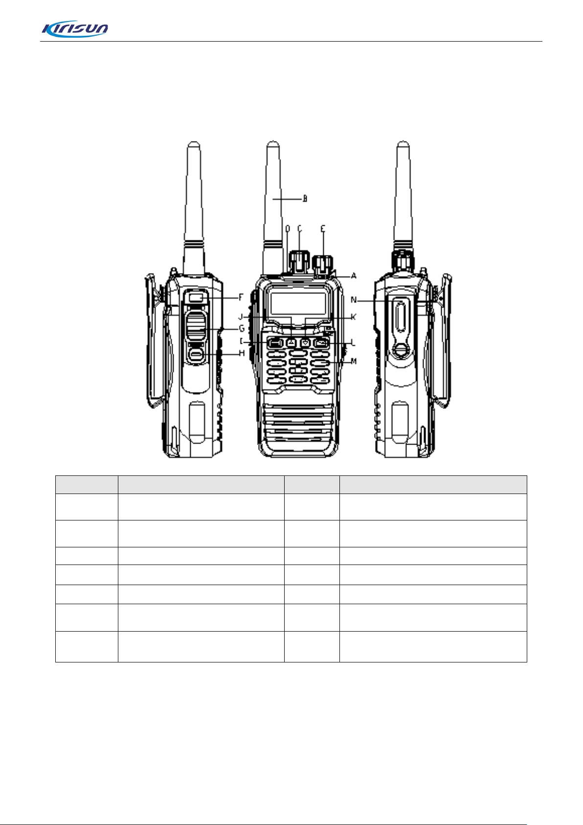
No. Part Name No Part Name
A LED Indicator H Programmable Button (SK2)
B Antenna I Return Key
C Channel Selector Knob J Up Key/Menu
D Emergency Button K Down Key
E On/Off/ Volume Control Knob L Con f irm Key
F Programmable Button (SK1) M Keypad
G PTT Button N
Earphone/Programming
Connector
2.2. LED Indicator
• The LED glows red: The radio is transmitting.
• The LED glows green: The radio is receiv ing (voice mail, messa ge, dat a) or ac tivit ies on the channe l are
Page 2 of 65
Page 6
TP660 Service Manual
ANT
LPF
RF AMP
Q505
MCF
IF AMP
Q507
GT3136
450K
AF AMPAF PA
SPK
D501
D503
D504
XF501
49
.95MHz
U102 NJM2902
IC101
TDA
8547
TX/
RX
SW
BPF
BPF
MIXER
CF501 450H
16.8MHz
TCXO
16.
8MHz
To 50.4MHz
Q605
X
601
Q509
450_IF AMP
CODEC
U201
HR
_C
5000
Q
506 3SK318
PLL
2
SK
72310
Loop
Filter
TX VCO
RX VCO
Buffer
PA
Pre
-driver
PA
driver
PA
Final
Q504 2
SC
3356 Q
503 2SC
3356 Q502 RD01 Q501 RD07
MIC
AF
AMP
CODEC
MOD_I
MOD_Q
U103
NJM2100
ANT
LPF
D501 D503
D504
TX/RX
SW
16.8MHz
TCXO
X601
U201
HR_C5000
PLL
2SK72310
Loop
Filter
TX VCO
Buffer
PA
Pre-driver
PA
driver
PA
Final
Q504 2SC3356 Q503 2SC3356 Q502 RD01 Q501 RD07
MIC
AF
AMP
CODEC
MOD_I
MOD_Q
U103
NJM2100
BATT+
APC
APC
U502
detected.
• The LED glows orange: The radio is sc anning.
3. Circuit Description
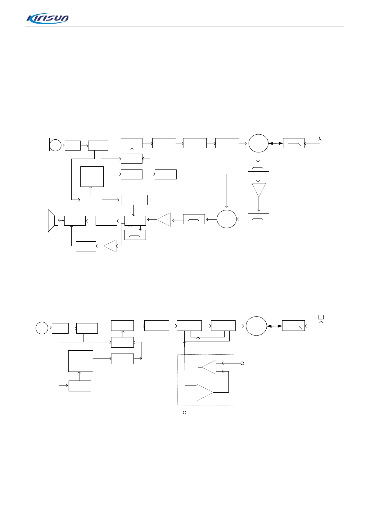
3.1. Tx/Rx Signal Proce du r e
Figure 3-1 RF Princ iple of Rec e iv er
3.1.1. Tx Circuit
Figure 3-2 Tx Circ uit Diagram
Tx circuit mainly includes four parts below:
• RF Power Amplifier Circuit
The carrier signal generated by VCO will be modulated and preliminarily amplified before entering Tx
circuit. The signal will first pass a Π-type pure resistance attenuator R536 R537 R538 to realize the level
isolation between the power amplifier circuit and Tx VCO; then the modulation signal will enter the first
Page 3 of 65
Page 7
TP660 Service Manual
ANT
LPF
RF AMP
Q505
MCF
IF AMP
Q507
GT3136
450K
AF AMP
AF PA
SPK
D501 D503
D504
XF501
49.95MHz
U102 NJM2902
IC101 TDA8547
TX/RX
SW
BPF
BPF
MIXER
CF501 450H
16.8MHz
TCXO
16.8MHz
To 50.4MHz
Q605
Q509
450_IF AMP
CODEC
Q506
3SK318
PLL
2SK72310
Loop
Filter
RX VCO
U201
HR_C5000
U301
STM32F
300Hz
LPF
U101
CTCSS/DCS
level pre-drive amplifier (Q504) for preli minary amplification, and ge nerate a ce rt ain level isolation fro m the
next level amplifier; the amplified signal will then enter the next level pre- drive amplifier (Q503 and drive
amplifier (Q502 RD01)) for further power amplification so as to ensure that enough drive power sign al ca n
be offered to the end-level power amplifier (Q501 RD07) for final power amplification. After being
processed by the a set of amplifiers at several levels, the Tx signal will complete the output impedance
match through a microstrip line at the output terminal of the end-level power amplifier, so the output
power loss caused by impedance mismatch can be avoided. The Tx signal will enter the low pass filter
through the Rx/Tx switch.
• Low Pass Filter Circuit for Harmoni c Su ppression
Low pass filter which suppress harmonic is a high order low pass filt er consisting of lumped inductor and
capacitor. With this filter , the out-of-band harmonic wave and spurious s ignal can be further suppres sed
on the condition that the certain in-band f luctuation is satisfied.
• Auto Power Control Circuit ( APC)
The drain current from the drive power amplifier and end-level power amplifier passes the sampling
resistor (R559 R560 R561) where the drain current completes the conversion from current to voltage with
the subtraction circuit composed of the first operational amplification. The voltage will be compared with
the PAC control voltage value output by DAC (U301 pin 29) at the second operational amplifier, and the
deviation voltage will change the Tx power strength by controlling the grid bias voltage of power amplifier
tube(including drive lev el and end level).
• Audio Processing
The microphone convert the speech signal to speech electric signal, and the signal will be amplified by
U103 before being input in to ADC of codec (U201 HR_C5000) for s a mpling; it w ill then b e outp ut int o D SP
after audio being digitally processed, and sent to DAC for modulation signal conversion; the modulation
signal will be separate d into path I and Q for modul ating VCO, TCXO.
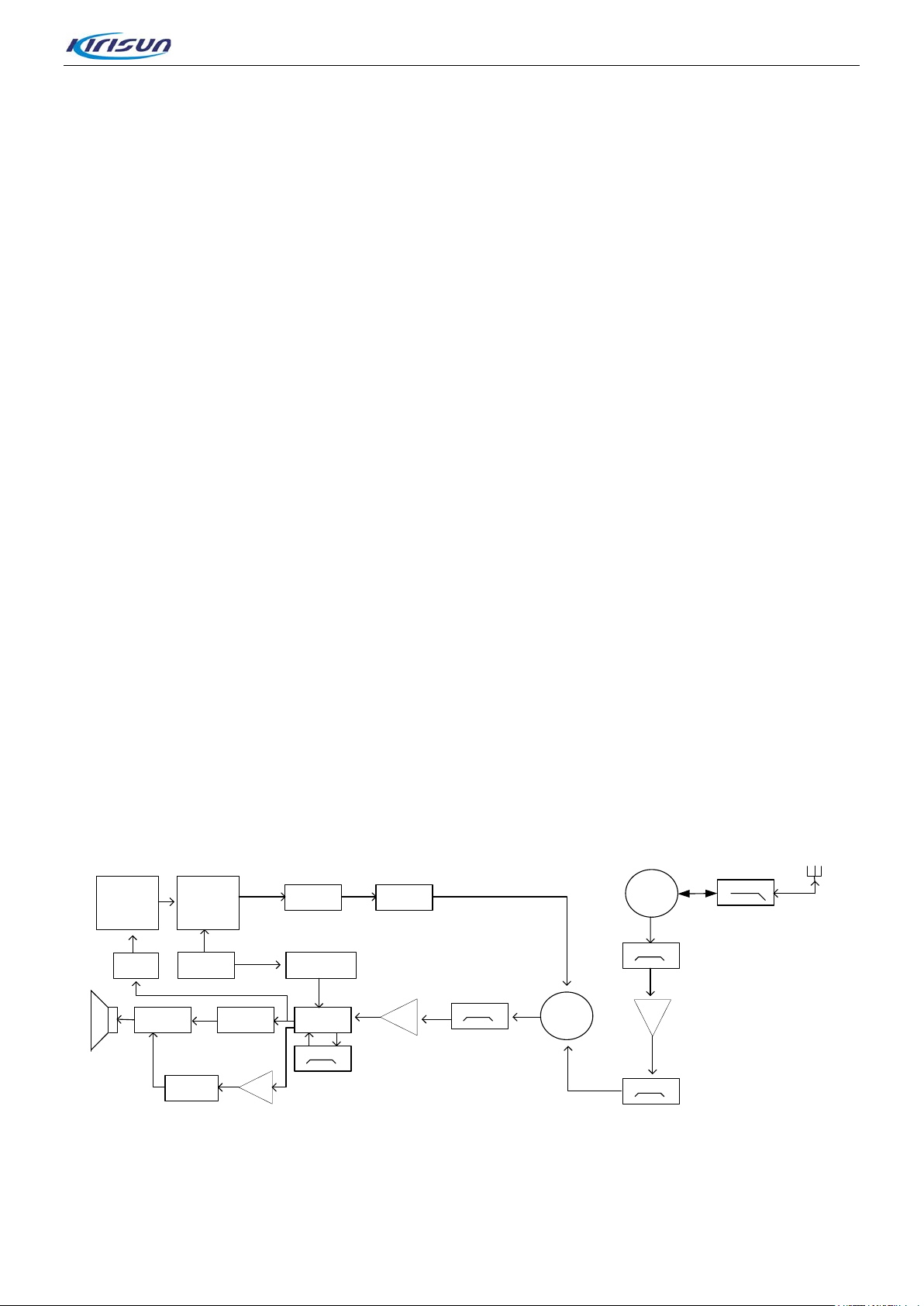
3.1.2. Rx Circuit
Figure 3-3 Rx Circuit Diagram
Rx circuit mainly includes:
RF band-pass filter, low noise amplifier, frequency mixer, IF filter, IF amplifier, IF processor and audio
Page 4 of 65
Page 8

TP660 Service Manual
circuit.
• Rx Circuit RF Part
The high frequency signal from low-pass filter passes the front stage electrically tunable band-pass filter
controlled by electric level and o utput by D AC (U301 PIN29 ) so as to filt er out t he out-of-band interfere nce
signal, sending ef fec tive b and-p ass signa l into the low noise amplifier (Q 505) . The amplified signa l p ass es
again the band-pass filter controlled by electric level and output by DAC so as to filter out the out-of-band
interference signal caused by amplification, sending effective high frequency signal into frequency mixer
(Q506).
The effective signal passes RF band-pass filter and low noise amplification and enters the frequency
mixer Q506, meanwhile, the first local oscillation generated by VCO passes the low-pass filter and enters
Q506 for making frequency difference with effective signal so as to generate the first IF signal. The signal
passes th e frequenc y selector network which consists of LC; it further suppresses the other carrier waves
other than the first IF, and increase the isolation between the frequency mixer and IF filter. The IF signal
will be filtered by the XF501 crystal filter, and then sent to the first IF amplifier(Q507) for am pl ifi cation
before being sent to the IC for IF processing (U501, GT3136).
The third harmonic frequency 50.4MHz produced by TCXO(X601 16.8MHz) is amplified by frequency
selector and become the second local oscillation signal source. The second local oscillation (50.4MHz)
mixes with the first IF signal in U501, generat in g t he s econd I F ( 450kHz). The second IF will be amplified,
limiting am plitud e inside U 501, and filter ed by the ceram ic filter CF50 1 450 kHz before going back to U501
for demodulating and outputting the audio signa l.
• Rx Circuit Audio Section
A. Digital Channel Audio Access: The second IF signal output from the eleventh pin of U501 is amplified
by Q509 and sent to U201 for ADC sampling and being converted to digita l signal; af ter t he digital audio
signal is compressed, decompressed and decoded by U301, U201 will complete DA conversion and
output audio signal from the 10th pin, and the audio signal will be amplified by U203 and sent to the
audio power amplifier IC101.
B. Analog Channel Audio Access: The audio signal out put from the 9th pin of U501 is ampl i fi ed by U102
and its unit circuit. The high frequency and low frequency will be removed from the audio signal,
keeping only the voice compone nt between 300 Hz to3000 Hz . The v oice compone nt will be ad juste d by
volume potentiometer and sent to audio power amplifier IC101.
C. Analog Channel CTCSS/DCS Signaling Access: The audio signal output from the 9th pin of U501
may include CTCSS/DCS signal. The 300Hz low-pass filter circuit composed of U101 filters out the
signals out of the CTCSS/DCS spect rum. After CTCSS/DCS is amplified, it will be sent to the 25th pin of
U301.
D. Analog Channel Squelch Circuit: The modulated output from U501 is sent to the frequency selector
noise amplifier which is composed of U501 internal noise amplifier and C555,R525,R524,C554,
C553,R527; the noise will be selected from the modulation si gnal and detected internally before being
outputting by the 14th pin and transformed as direct electric level to reach MCU U301; MCU identifies
the electric level strength and controls squelch.
Page 5 of 65
Page 9

TP660 Service Manual
16.8MHz
TCXO
U601
2SK72310
LPF
X601
Loop
Filter
TX VCO
RX VCO
LD
CS
DATA
PS
MOD_Q
MOD_I
RF
3.1.3. Frequency Synthesizer Circuit
Figure 3-4 Frequency Sy nthesizer Circuit Diagram
Frequency synthesizer circuit is composed of VCO and PLL, and it is the kernel module of the whole TRx
system. When transmitting, the circuit supplies accurate carrier frequency; when receiving, it supplies
stable local oscillati on signal. The circu it directly influences som e of the important functions in the system.
• PLL Working Principle
The 16.8MHz frequency generated by the reference crystal oscillator enters the frequency divider of PLL
chip, and becomes referenc e freque ncy (i.e. step freque ncy f1). The frequency generated by VCO passes
LPF for filtering out the second harmonic wave and enters PLL chip for frequency division and gets
frequency f2. The frequency f2 compared with f1 on phase difference in phase comparator, producing
continuous pulse current. When the pulse current passes the loop filter, it starts to accumulate RC and
converts to CV voltage. The CV voltage is sent to the VCO varactor, directly controlling and adjusting the
VCO output frequency until CV becomes constant. PLL will be currently locked, and the stable frequency
output from VCO pass es t wo buffer amplifiers before entering the TR x access.
• The Working Principle of Voltage Controlled Oscillator
The voltage controlled oscillator applies oscillation mode of three point capacitor. It changes the control
voltage of varactor to get different output frequency. Rx VCO is composed of oscillator circuit and Q603.
Tx VCO is composed of osci llat or c ircuit and Q601, supplying car r ier w ave of TX signal.
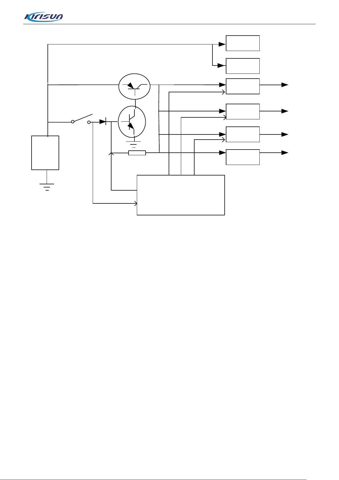
3.2. Power Section
Figure 3-5 Power Structure Diagram
Page 6 of 65
Page 10
TP660 Service Manual
Battery
SW401
POW_DET
POW_HOLD
RF PA
AF PA
U404
LDO
U403
LDO
U402
LDO
U401
DC-DC
5C
5R
5T
3.3V
Q401
Q402
U301
STM32F
SAVE
5RC
5TC
This radio applies 7.4V,2000mAh lithium battery, RF power amplification (Q501, Q502), AF power
amplification (IC101) , and direct battery power supply.
The power circuit is composed of power-on/off circuit, 5C, 5R, 5T, and 3.3V DC-DC voltage stabilizing
circuit.
Power-on Circuit: When SW 401 is closed, the B level of Q402 becomes high electrical level, and the
switch tube Q401 becomes conductive. The power supplies electricity for every power module through
Q401, when MCU is powered on, POW_HOLD will output high electric level to keep Q401 constantly
conductive so as to turn on t he r adio.
Power-off Circuit: When SW401 is cut off, POW_DET test pin becomes low electric level, and
POW_HOLD pin of MCU will first st ays on high e lectric level for a w hile before out putting low elect ric level.
The Q402 B level thus becomes low electric level, cutting off the switch tube Q401 and the power to turn
off the radio.
5C voltage stabilizing circuit: U404 applies 5V LDO voltage stabilizer and supply 5v power for PLL circuit.
Meanwhile, the 67th pin of U301 outputs high and low electric level to control the enable pin of U404,
making the voltage stabilizer switches between 5V and 0V so as to realize the functions such as energy
saving and Tx/Rx switch.
5R voltage stabilizing circuit: U403 applies 5V LDO volt age sta bilizer, and supplies 5V power for Rx circuit.
Meanwhile, the 66th pin of U301 outputs high and low electric level to control the enable pin of U403,
making the voltage stabilizer switches between 5V and 0V so as to realize the functions such as energy
saving and Tx/Rx switch.
5T volt age st abil izing c ircuit : U402 applies 5V LDO voltage stabilizer, and supplies 5V power for Tx circuit.
Meanwhile, the 34th pin of U301 outputs high and low electric level to control the enable pin of U402,
Page 7 of 65
Page 11

TP660 Service Manual
making the voltage stabilizer switches between 5V and 0V so as to realize the functions such as energy
saving and Tx/Rx switch.
voltage stabiliz ing circuit:U401 applies 3.3V DC-DC voltage stabilizer,and supplies 3.3V power for U201、
U301、U302、U307.
4. Function Description and Parameter Settings
4.1. Conventional Functions
• Supports private call, group cal l, al l cal l i n dig ital mode
• Supports end-to-end voice encryption, data encryption
• Supports short message
• Supports radio check, remot e monitor, radio disable and radio enable dig it al si gnalin g in DMR st an dard.
• Supports CTCSS/CDCSS on ana log mode
• Supports DTMF system on ana log mode
• Supports emergency alarm feat ur e
• Supports digital channel sc anning, analog channel scanning, and digital/an alog mix scanning.
• Supports a maximum of 1000 channels
• Supports a maximum 250 regio ns with each region contai ning 128 channels.
• Supports a maximum of 512 contacts.
• Supports LED, and alert tone which indicates option
• Supports programmable selection between 12.5 kHz and 25 kHz channel spa cing.
• Strength indicat ion for r eal time signal
• Battery power indication
4.2. Function Parameter Settings
The radios are set with default value when t hey are o ut of the factor y. But due to the different requ irement s
by the users, the rad io ma y be reset with operational frequency, channel parameter, scanning, encryption,
etc. Therefore, Kirisun specially designs a user programmable software which is interface-friendly,
operation-easily and display-visually to complet e t he parameter sett ings for the radio.
• Steps for p ar am eter settings are as below:
Step 1. Confirm that the right ver sion o f TP 660 us er progra m mabl e sof tw are is installed on the computer.
Step 2. Confirm that the right version o f TP660 USB driver software is instal le d on t he computer.
Step 3. Use TP660 programmable lead supp lied by Kirisu n to connec t the r adio w ith c omputer US B port.
Step 4. Confirm that the radio is powered on.
Page 8 of 65
Page 12
TP660 Service Manual
Step 5. Operate TP660 user programming software.
• Steps for installing TP660 user pr ogrammable software are as below:
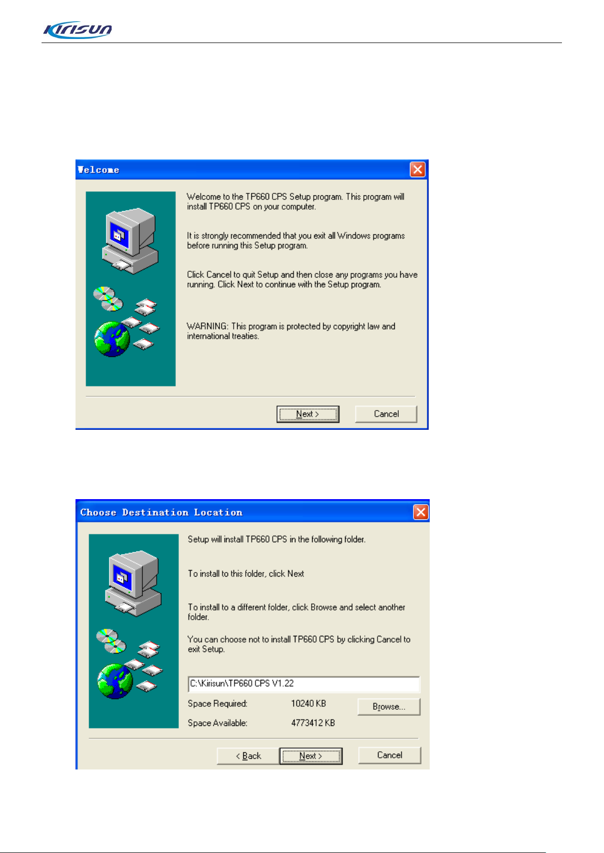
Step 1. Double click the installat ion file, and the interface in Fig ur e 4-1 pops up.
Figure 4-1
Step 2. Click “Next” to enter the next interface for selecting software installation path.
Figure 4-2
Page 9 of 65
Page 13
TP660 Service Manual
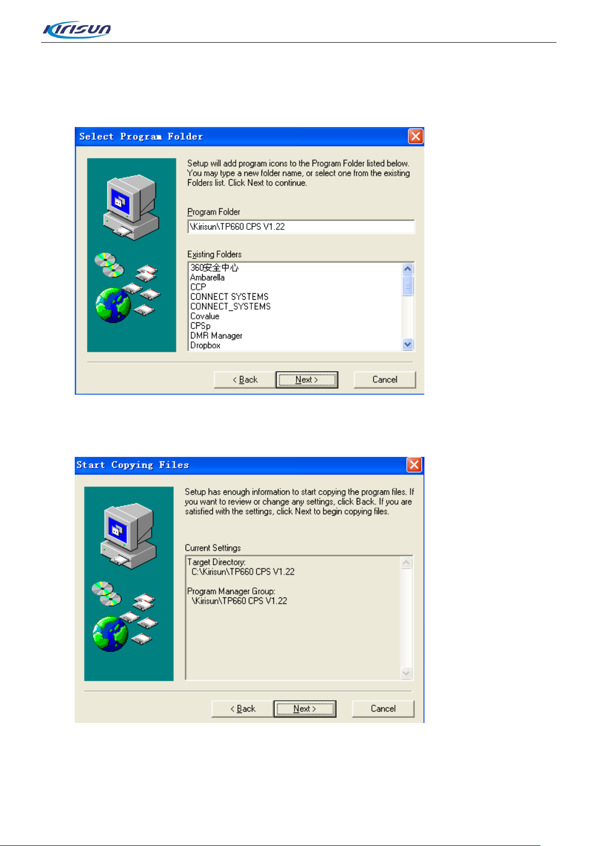
Step 3. As shown in figure 4-2, the user can click “Browse” to select the s oftware inst all at ion path or the
default installation path. Click “Next ” t o ent er t he installation confirmation interface.
Figure 4--3
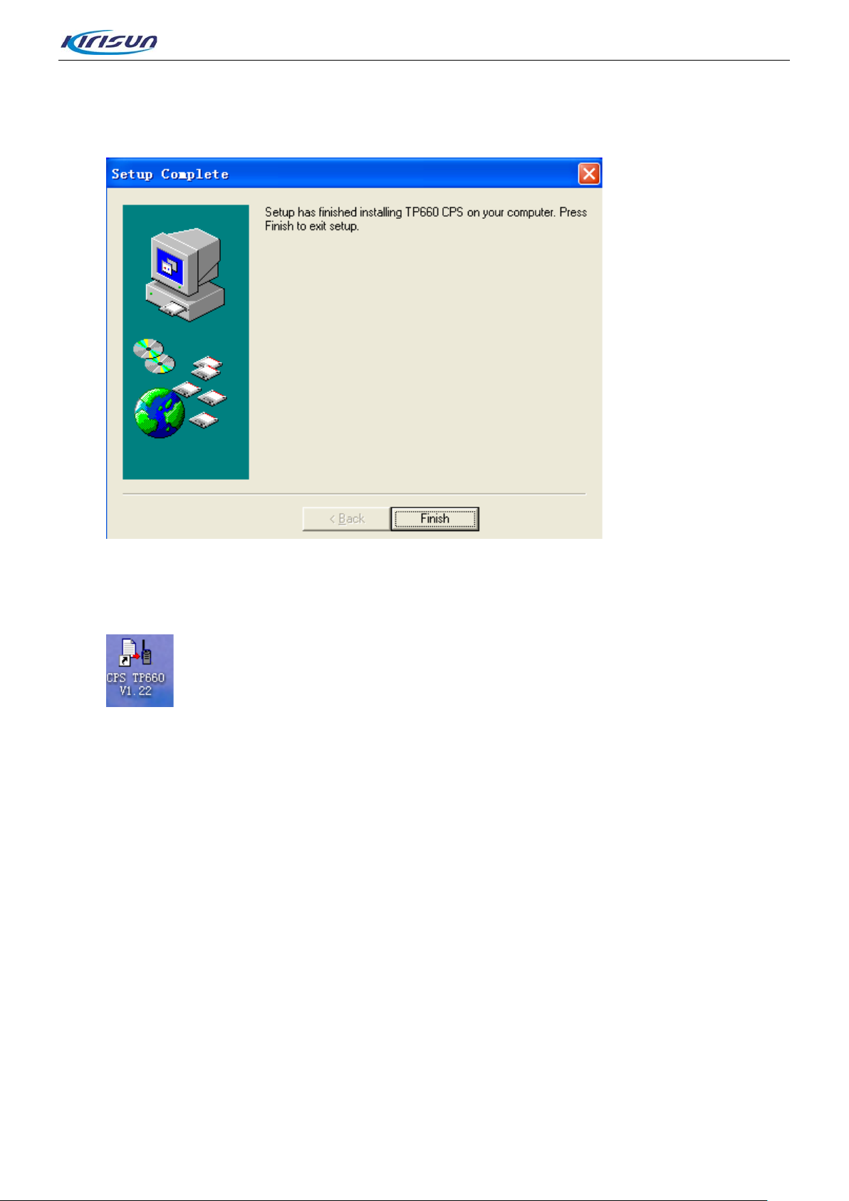
Step 4. Click “Next” to enter the installation completion interface.
Figure 4-4
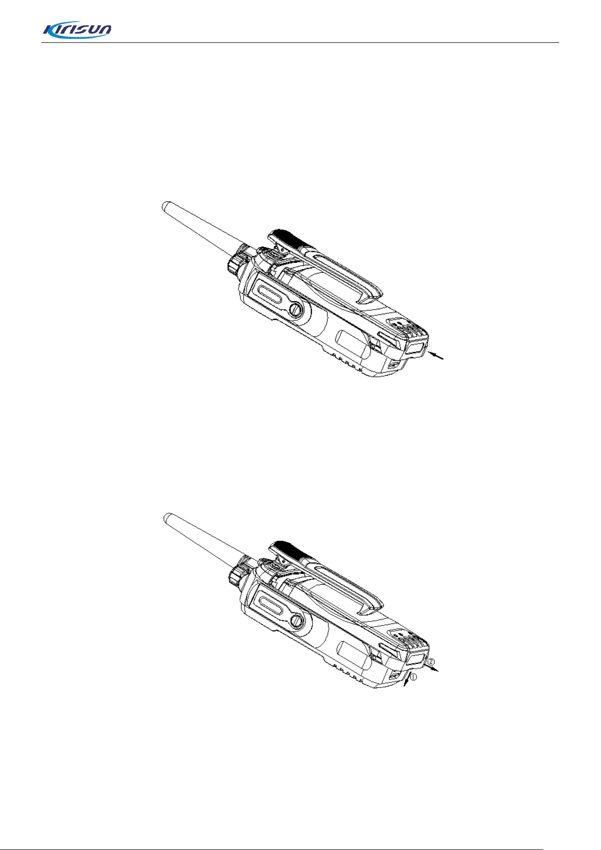
Step 5. Click “Finish” to complete the software installation.
Page 10 of 65
Page 14
TP660 Service Manual
Figure 4-5
Step 6. After the installation, double click T P660 user programmable software. See figur e 4-6.
Figure 4-6
The user can read the current parameter settings from the radio through TP660 user programmable
software, and the parameter can also be res et .
Note:
1. Wrong parameter sett in gs may cause malfunction. Normally, rewrite the correct parameter settings can
solve the problem.
2. Before rewriting the parameter settings, reading th e parameter settings out of the radio for bac k-up is
strongly recommended i n case t hat the recovery is neede d once the radio becomes faulty.
5. Assemble and Disassemble Instructions
This radio is sophisticated communication equipment with compact, precise mechanism. Please be
careful during the att ac hing and detaching.
The attaching and detaching instruct ions are as below:
Page 11 of 65
Page 15
TP660 Service Manual
5.1. Attaching and Detaching the Batter y
Attaching the battery
Press the belt clip and push the battery pack forwards in the arrow direction until a click is heard, which
indicates that the battery pack is properly fixed. (see figure 5-1)
Figure 5-1
Detaching the battery
When detaching the battery, press the latch in the direction shown in figure 5-2, and use other hand to
push the battery backwar ds unt i l it is separated from the rad io.
Figure 5-2
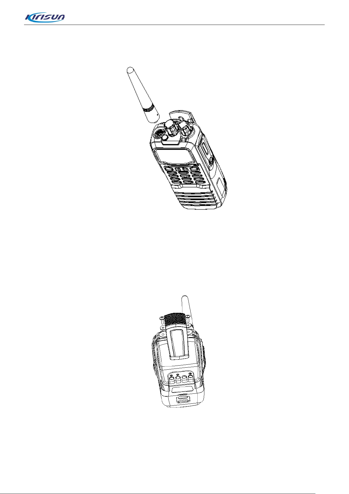
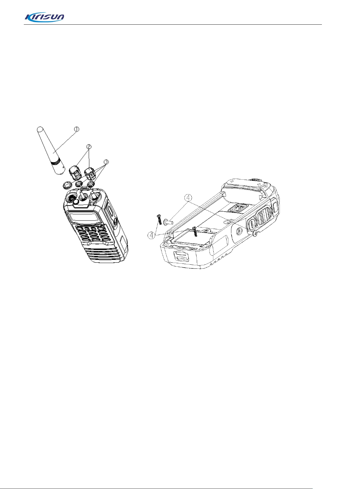
5.2. Att aching the Antenna
Hold the antenna base, turn the antenna clockwise into the interface on the radio top until it is fastened.
Page 12 of 65
Page 16
TP660 Service Manual
(see figure 5-3)
Figure 5-3
5.3. Attaching the Belt Clip
Step 1. Press the belt clip and align the two screw holes with those on the back aluminum shell. (See
figure 5-4)
Step 2. Fasten the two screws.
Figure 5-4
5.4. Separating the Shell from the Chassis
Step 1. Detaching the antenn a. (see figure5-5 and 5-6)
Page 13 of 65
Page 17
TP660 Service Manual
Step 2. Remove the knob and snap ring.
Step 3. Remove the two knob nut and antenna nut.
Step 4. Remove the four screws a s show n in the figure below.
Step 5. Insert a flat screw driver int o t he seal groove of the aluminum bracket, and push it upwards to
remove the zinc cover; push t he a luminu m brac ket bac kwards to make it out o f t he she ll, and t a ke out
the flex cable from the socket.
Figure 5-5 Figure 5-6
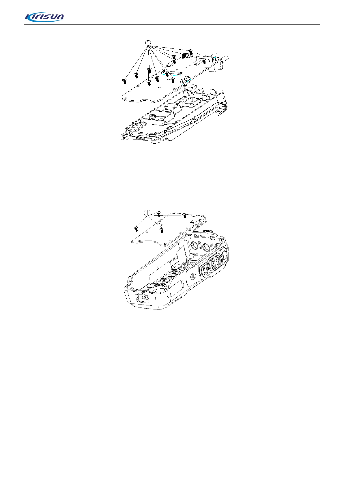
5.5. Disassemble the Main Board f r om the Chassis
Step 1. Remove the main board screw s and PTT, PCB screws.(see figure 5-7)
Step 2. Remove the top waterproof ring and use a soldering iron to solder of f the antenna, then the mai n
board can be separat ed from the aluminum bracket .
Figure 5-7
Page 14 of 65
Page 18
TP660 Service Manual
5.6. Separating the Keyboard from the Front Cover
Remove the four front cover sc r ew s to separate the keyboar d from the front cover.(see figure 5-8)
Figure 5-8
After the detachment above, the mainte nance and adjustment can be do ne accordingly.
Page 15 of 65
Page 19
TP660 Service Manual
1
2 3 4 5 6 7 8 9 10 11 12 13
14
15 16
23
24
16
25
26
27
28
17
18
19
20
21
22
2930313233343536
37
38
39
40
27
41
42
44
45
46
47
48
16
43
15
49
1
PT7800 PTT cover(cover die) PC+ABS, black, 2010B, pb-free
1
3
PT7800 lens double-si ded adhesive NITTO57120,43.4*28.2MM, supplier:
1
pb-free
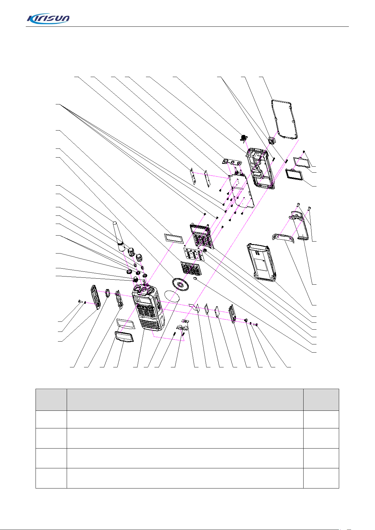
5.7. Exploded View
No. Part Name, Specif i cat i on and Model Number Unit
2 PT7800PTT keypad silica gel, black, hardness 60 degrees, supplier:
Mingkun, pb-free
Xinlongda, pb-free
4 PT7800 TP660 lens PC, transparent, screen printing KIRISUN+ black,
1
1
Page 16 of 65
Page 20

TP660 Service Manual
5
TP660 shell PC+ABS, black, 2008B, #4-40 nut,pb-free
1
7
PT3208 spring material: spring st eel, nikle-plated, wire diameter 0.2,D
2
flexible board, ;27.5X24.3MM;2 layers, pb-free
12
TP660-02 interface board, TP660-02_IO_140818, 2.0MM thick;
1
13
PT7800 earphone cov er (cover die) PC+ABS, black, 2008B,1405mode
1
IP black、pb-free
pb-free
19
spacer,φ3.0*5.0*0.3mm
2
21
TP660 keyboard jacking, pb-free
1
22
KB-78B battery, lithium polymer battery, 7.4V,2000mAh, pb-free
1
23
PT7800top cover (cover die) PC+ABS, black,s 2008B, pb-free
1
24
KBJ-09 belt clip, 568 belt clip (end item),PC+ABS, black, pb-free
1
26
PT7800 roof cover 0.5MM,SUS304,pb-free
1
6 PT7800 horn net material: black 250+nitto57120b,diameter φ36mm*
1
0.3mm thickness, with two-sided adhesive
external diameter 2,H length 9.5,circling 11
8 PT7800 1.2MM,IP vacumm plating, supplier: Junyu, pb-free 1
9 PT7800 battery latch (cover die) PC+ABS, embedded latch baffle, black,
1
2008B, pb-free
10
TP660-02 accessory FPC TP660-02_ACC_FPC_140819; 0.1MM thick;
11 TP660 earphone PCB board, double-sided adhesiv e 0.4mm thick,
1
1
NITTO 57120B double-sided adhesive
FR4,12.5X25MM; four layers,pb-free
changing,pb-free
14
R M3*4 earphone cover screws 、SUS303、# 4-40 thread、
vacuum plating,
1
15 O-type ring, D2.4X1.0MM, pb-free 2
16 M2.5*8 cross round flat machine screw. material: hardened
4
iron,Φ2.5mm*8mm. Cross round flat black zinc-plated machine thread,
metric coarse thread.
17 PT7800 mic-head waterproof p ad. Material: DY-E002A; breathable film,
1
φ6.6xφ4.4, pb-free
18 PT7800 digital keypad. METAL DOME sixteen D6 square metal dome,
1
20 R 558 mic cover; material: silica gel, hardness 40,orange, no surface
1
processing
25 PT7800 roof waterproof ring, silica gel, orange, hardness 60 degrees,
1
pb-free
27 M2*4 cross round flat machine screw. material: hardened iron,
19
Φ2mm*4mm cross round flat nickel-pl ated mac hine thread, metric coarse
thread
28 PT7800 big w aterpro of ring, silica gel, black, hardness 40 degrees, pb-free 1
29 PT7800pedesta l w at er pr oof pad, silica gel, black, hardness 60 degrees,
1
pb-free
30 M2*8 plum-type thick-headed machine screw. material: hardened iron,
2
Φ2mm*8mm plum-type thick-headed nickel-plated m achine threa d, metric
Page 17 of 65
Page 21

TP660 Service Manual
coarse thread
32
PT7800aluminum alloy bracket; aluminum alloy (ADC12),grinding,
1
pb-free
40
Antenna. R antenna 400-470MHZ,length:140mm.` SMA-K,TPEE black
1
41
PT7800 channel knob ABS, black , 2012B, pb-free
1
φ10mm, 3.5mm thick, black passivation
47
PT7800 guide beam PC, transparent, pb-free
1
49
PT7800 PTT side cover PC+ABS, black, 2008B/2010B, pb-free
1
31 RF coaxial connector an al og r adio SMA-J, flange plate (558,hole14mm,
chip length10.5mm)
polishing, pb-free
33 PT7800top waterproo f pad silica gel, black, hardness 60 degrees, pb-free 1
34 TP660 mainboard jackin g, pb-free 1
35
36 PT7800 PTT button metal dome. three D6 square metal dome,pb-free 1
37 R 6500LCDdust-proof pad. material: black foam 1
38 PT7800 keypad black +637C + white(laser carving), hardness 60 degrees,
39 7800 horn PT7800-05 Φ40,H=17±0.1mm,impedance16Ω, power 1.5W.
42 PT7800 volume knob ABS, black, 2012B, pb-free 1
43 R 3118/3208 knob s nap r ing. material: spring st eel 1
44 PT7800 programming knob snap ring. 0.3MM,stainless steel, pb-free 1
45 Switch nut. material: brass, internal diameter M6mm, external diam eter
TP660 PTT board TP660-02_PTT_131127.PCB;9.6X46.6MM;0.6MM;
FR-4, two layers, pb-free
pb-free
1
1
1
1
2
46 Antenna nut. internal d iameter M8.7mm, e xternal diameterφ12mm,
3.6mm thick, black zinc plated,
48 PT7800emergency keypad silica gel,orange, hardness 60 degrees,
pb-free
1
1
6. Adjustment
During the maintenance, it is necessary to test and adjust the radio’s technical parameters after changing
components.
6.1. Component s for A djustment
(1) Antenna connector conver t er
(2) Universal connector
Page 18 of 65
Page 22

TP660 Service Manual
Low
Intermediate/low
Intermediate
Intermediate/high
high
MHz)
MHz)
Requirement
1.Enter computer adjustment mode
6.2. Adjustment Test Method
6.2.1. Frequency Description
Model TP660(400-470)
Channel
Tx frequency
(MHz)
Rx frequency
(
Model TP660(134-176)
Channel
Tx frequency
(
Rx frequency
(MHz)
frequency
400.025 417.025 435.025 452.025 469.975
400.25 417.25 435.25 452.25 469.95
Low
frequency
136.025 145.025 155.025 162.025 173.975
136.25 145.25 155.25 162.25 173.95
6.2.2. Test Tools
frequency
Intermediate/low
frequency
frequency
Intermediate
frequency1
frequency
Intermediate/high
frequency
frequency
high
frequency
• Integrated tester
• Programming lead
• AEROFLEX 3920
• Spectrum analyzer FSU
6.2.3. Tx Test and Modulation
Item Steps
2.Enter “RF stability adjus tment”,
Frequency stability
3.Adjust PC software valu e, and observe integrated
tester frequency value.
4.Adjust to nominal freque ncy ±100Hz
Specification
≤0.5ppm
Page 19 of 65
Page 23

TP660 Service Manual
1. Enter computer adjustment mode.
adjusts the bit error r at e also adjusts fre quency deviation;
methods above).
Tx high power
Tx low power
I path and Q path
amplitude
adjustment for
analog transmit
1. Enter computer adjustment mode.
2. Enter adjustment mode “ Tx hig h power”
3. Adjust PC software value, obs erve integrated tester
frequency value..
4. Adjust to the nominal test pow er .
UHF:4.2±0.2W. VHF:5W±0.2W
5. Adjust the frequencies by turns
2. Enter modulation mde “Tx low p ower”,
3. Adjust PC software value; obs erve integrated tester
power value.
4. Adjust to nominal test pow er 1± 0. 2W.
5. Adjust the frequencies by turns.
1. Enter computer adjustment mode;
2. Enter “analog Tx I path amplitude and Q path
amplitude” to adjust I oat h value.
3.Observe FM Deviation as 1.95±0.05kHz;
5. Click “OK” to save
UHF:3.8-4.5W
current: less than
1.8A
VHF: 4.5-5.2W
current: less than
1.8A.8A
0.8-1.2W
current: less than1A
1.9KHZ~2.0KHZ
I path and Q path
amplitude
adjustment for
digital transmit
CTCSS frequency
deviation and
wave
1. Enter computer adjustment mode;
2. Enter “digital Tx I path amplitude a nd Q path
amplitude ”.
3. Click digital adjust ment item, and adjust Q p at h( see
figure 6) to adjust the digital frequency deviation in the
range between 1.9KHZ and 2KHZ; adjust the bit error
rate through the I path ad j ust m ent, and the I path w hich
the Q path which adjusts digital frequency deviation also
adjusts bit error rat e. When the Q path is turned up, the I
path also needs to be turn ed up or turned down. Adjust
the channel 1 within the specif ied range and click ok
before clicking the next channel for adjustment.
(Channel 3. 5. 7. 9 can be adjusted in turn based on the
1. Enter computer adjustment mode.
2. Enter the adjustment mode one by one
“CTCSS(67Hz)”, “CTCSS(51.4Hz)” “CTCSS(254.1Hz)”
3. Adjust PC software value and o bs er ve integrated
tester frequency deviati on value.
4. Adjust to the nominal frequency deviation: 350±5 0Hz.
5. Adjust the frequencies i n turn.
6. Check the frequencies in t ur n.
1.9KHZ~2KHZ
FSK EER≤5%Hz
200±200Hz.
< 15mV
Page 20 of 65
Page 24

TP660 Service Manual
Requirement
、
>
DCS frequency
deviation and
wave
1. Enter computer adjustment mode..
2. Enter the adjustment mode “ DC S frequency devia tion”,
3. Adjust PC software value and o bs er ve integrated
tester frequency deviati on value.
4. Adjust to nominal frequ ency deviation: 350±50Hz.
5. Adjust the frequencies i n t ur n.
6. Check the frequencies in turn.
350±150Hz
Modulation
distortion
Tx SNR Observe SNR form value
4FSK Tx error
Analog & digital
ACP
Spurious emission Observe spectrum analyzer display value
Observe distortion for m v alue
1.Select 3920 and put it on the DMR test int erface; set
the receiver frequency as t he low frequency of the radio
Tx frequency, Press PTT button to trans mit and re ad the
FSK Error on the apparatus. (select the test average
value);
2.Test the intermediate frequency and high freque ncy
channel with the same met hod.
Observe adjacent channel pow er dis play value
<3%
N:>40dB.
<5%
N:<-60dB.narrow
band)
<1GHz:<-36dBm;
>1GHz:<-30dBm.
6.2.4. Rx Test and Modulation
Item Steps
1. Enter the computer mo dul ation mode.
2. Enter the modulation mode”Rx se nsitiv ity”, c lick frequency 1
RF Rx
Sensitivity
3、5、7、9 one by one.
3. Observe the integrated t es t er spect r um analyzer property ;
adjust PC software value, Rx SINAD
4.Setting: Rx frequency -24.975MHz(*1、*2、*3、*4); set the
signal ass -40dBm,SINAD<7dB.
12d.
Specification
SINAD>=12dB
N:-118dBm
Page 21 of 65
Page 25

Squelch
4. Adjust frequency 1、3、5、7、9、one by turns.
4. Adjust frequency 1、3、5、7、9、one by turns.
Distortion
Observe SNR form value.
no interrupter
level9 on
Squelch
level9 off
Squelch
level1 on
Squelch
level1 off
TP660 Service Manual
1. Enter the computer mo dul ation mode.
2. Set the channel as current t est frequency.
3. Enter the modulat ion m ode ” SQL9 on”, clic k star t and sw itc h to
the next frequency when the number is stable.
4. Adjust frequency 1、3、5、7、9、one by turns.
1. Enter the computer mo dul ation mode.
2. Set the channel as current t est frequency.
3. Enter the modulation mode ” SQL9 off ”
, click start and switch to the next frequency when the number is
stable.
.4. Adjust frequency 1、3、5、7、9、one by turns.
1. Enter the computer mo dul ation mode.
2. Set the channel as current t est frequency.
3. Enter the modulation mode ” SQ L1 on ”, click start and switch
to the next frequency when the number is stable.
1. Enter the computer mo dul ation mode.
2. Set the channel as current t est frequency.
3. Enter the modulation mode ” SQ L1 off ”
”, click start and switch to t he next frequency when the number is
stable.
Input -115dBm to
turn it on,-120dm
to turn it off
Input -115dBm
and turn
on,-120dm and
turn off
Rx
Rx SNR
CTCSS/CDC
SS Decoding
BER Test
Observe SNR form value.
1.Set the output of 3920 as -118dBm.
2.Enter bit error rate test it em; click start and observe bit error
rate.
7. Technical Functions and Index
General Specificatio n
Frequency Range UHF1: 400-470MHz VHF: 136-174MHz
<3% (4 bars)
Decoded
successfully and
EER≤5%
Channel Capacity 1000
Channel Spacing 12.5kHz/25kHz
Weight 280 kg(with batter y and antenna)
Page 22 of 65
Page 26

TP660 Service Manual
Measurement
113mm*54mm*34mm
(H*W*T)
Battery Capacity 7.4V 2000mAH lithium-ion battery
Working hour
(5-5-90)
analog:13.5 hours
digital:15 hours
Environment Specification
Working Temperature -30 ℃~+60℃
Storage Temperature -40 ℃~+85℃
Waterproof and
IP67
Dust-proof
IEC 61000-4-2
Statics Prevention
±4kV±8kV (air)
American Military Standard MIL-STD-810 C/D/E/F/G
Damp proof MIL-STD-810 C/D/E/F/G
Shock and Oscillation MIL-STD-810 C/D/E/F/G
Receiver Specification
Frequency Stability ±1.5ppm
Analog Rx Sensit iv it y 0.3uV(12dB SINAD)/0.22uV(12dB SINAD,typical)
Digital Rx Sensitivit y 0.3uV(5% bit error rate)
Intermodulation ETSI:65dB TIA603:70dB
Adjacent Channel Selectivity ETSI/TIA603:60dB@12.5kHz,70dB@25kHz
Spurious Response Suppression ETSI/TIA603:70dB
Conductive Spurious Radiation -57dBm
Block ETSI:84dB TIA603:80dB
Rated Audio Power 0.5W
Rated Audio Distortion <3%(typical)
Hum and Noise -40dB@12.5kHz/-45dB@25kHz
Page 23 of 65
Page 27

TP660 Service Manual
Input Impedance The minimum circuit load high input imped ance
Audio Response +1dB ~ -3dB
Transmitting Specification
Frequency Stability ±1.5ppm
Tx Power UHF: 1W/4W; VHF:1W/5W
Hum and Noise -40dB@12.5kHz/-45dB@25kHz
Conductive Radiation Spurious -36dBm@<1GHz,-30dBm@>1GHz
Adjacent Channel Power 60dB@12.5kHz,70dB@25kHz
FM Modulation 11K0F3E@12.5kHz,16K0F3E@25kHz
4FSK Modulation
Modulation Limit ±2.5kHz@12.5kHz,±5kHz@25kHz
Audio Response +1dB~-3dB
Audio Distortion 3%(typical)
Vocoder Type AMBE++
Digital Communication Protocol ETSI TS 102 361-1, -2, -3
12.5kHz(data only):7K60FXD
12.5kHz(data + voice):7K60FXE
8. Maintenance and Test Equipment
During maintenance and adjustment, the major equ ip me nt and apparatus bel ow w ill be used.
Equipment Major Specification
Frequency Range 10MHz-3GHz
RF Signal Generator
Power Meter
Frequency Deviation
Meter
Digital Voltmeter
Oscilloscope 30-100MHz
High Sensitivity Frequency Range 100-1000MHz
Modulation Frequency modulation and ext er nal modulation
Output -127dBm/0.1uV-> 47dBm/1mV
Input Impedance 50Ω
Operation Frequency 100MHz-1000MHz
Measurement Range About 10W
Frequency Range 100MHz -1000MHz
Test Range DC 10Mv-10V
Page 24 of 65
Page 28

TP660 Service Manual
Frequency Counter
Frequency Stability ±0.2ppm or lower
Ammeter
5A
Voltage Range 1mV-10V
Power
signaling of the two r adios d if fer. Please reset
C.Beyond the communication scope.
The Tx frequency and Rx freq uency d if fer. Please select the same
C.Beyond the communication scope.
The Rx green
without any voice
Poor contact in earp hone i nterface b oard. If so, please ch ange the
Audio Voltmeter
Audio Signal Generator
Distortion Tester
Spectrum Analyzer Test Range 100-3GHz or highe
16Ω Dummy Load
Voltage Stabilizing
Frequency Range 50Hz-10kHz
Frequency Range 50Hz-5kHz or higher
Output 0 V-1V
capacity 3% or lower at 1kHz
Input Electric Level 50mV-0Vms
About 16Ω,3W
Output Voltage 5V-30V,Current:5A
9. Troubleshooting
No. Problem Cause and Solution
A.Check if the battery is in low power . If the battery is low, please
charge it or change it.
B.Check if ther e is poor c ontac t in the power-o n kno b. Please ch ange
the knob and try again.
C.The power connecting w ir e is in poor contact with the battery.
Please reinstall it and tr y again.
D.The reverse power connec t i on leads to the power prot
ective tube F401 being turned on. Please change the protect iv e t ube
and try again.
A.The frequencies between the two radios differ. Please select the
same channel with frequency.
B.The CTCSS/CDCSS
with your computer.
1
3
Failed to turn on the
radio
Failed to
communicate with
each other
A.Poor contact of the antenna. Please fasten the antenna.
4
5
6
Failed to receive the
signal
indicator lights up
The programming is
abnormal
B.
Tx/Rx frequency again.
A.Check if the volume is at its lowes t level. If so, turn on t he volume.
B.Check if the speaker is br oken. If so, please change t he speaker.
A.Wrong wire connection. Please check if the co nnection is right.
B.Check if the computer USB driv e is insta lled. If not, please inst all it
properly.
C.
interface board.
Page 25 of 65
Page 29

TP660 Service Manual
C180
0-271J
G
0-332K
7R
RU
BL112-38RU
220M
TP series ( level A)
Appendix
List 1 Material List(Electronic Section 400-470MHz)
Keyboard
No Part No. Specification Quantity Location
C126, C111,
2CC1-10-C0G50
1
0-101J
1005,100P±5%,50V,C0
G
14
C119 ,C121,C124,C125, C 150,C15
1,C152,C153,C154,C155,C156,
2CC1-10-X7R50
2
0-103K
2CC1-10-X7R16
3
0-104K
2CC1-10-C0G50
4
0-221J
2CC1-10-C0G50
5
2CC1-10-X7R50
6
0-471K
2CC1-10-X5R6R
7
3-105K
2CC1-10-X7R50
8
3FW1-S0603-50
9
1032
3CF1-BL112-14
10
RL
3CF1-BL112-10
11
RL
3CF1-BL112-38
12
1005,10nF±10%,50V,X7
R
1005,100nF±10%,16V,X
7R
1005,220P±5%,50V,C0
G
1005,270P±5%,50V,C0
1005,470P±10%,50V,X7
R
1005,1uF±10%,6.3V,X5
R
1005,3300P±10%,50V,X
S0603-S-0.5A,32V,SAR
T
Interval 0.5mm,14 core,
BL112-14RL
Interval 0.5mm,10 core,
BL112-10RL
interval 0.5mm,38 core,
3 C133,C157,C162
7
5 C143,C144,C147,C190,C191
6 C100,C103,C108,C109,C127,C128
6
6 C101,C102,C131,C166,C167,C181
2 C192,C193
1 F101
1 CN102
1 CN103
1 CN101
C104, C110,
C130 ,C145 ,C160 ,C170, C11 8
C117,
C129 ,C132 ,C146 ,C148, C15 9
13 1DP1-BV08C BV08C 11
14
15
16
17
2CT1-TP20-1004R7M
2CT1-TS32-100-
5FE1-BLM11A22
1SPT
5FE1-BLM21P30
0S
2012,4.7μF±20%,10V,T
P series ( level P)
3216,22μF±20%,10V,TS
1608,BLM11A221SPT/B
LM18AG221S(0138-05)
2012,BLM21P300S/BLM
21PG300S(0149-05)
D111,D112,D113,D114,D115,D116
,D117,D118,D119,D120,D121
2 EC120, EC131
1 C105
6 L101,L105,L107,L102,L103,L104
1 L106
Page 26 of 65
Page 30

TP660 Service Manual
DTC144EE(26),SOT323
22
2RS1-10-000O
1005,0Ω
1
R123
23
2RS1-10-220J
1005,22Ω±5%
2
R134,R135
24
2RS1-10-104J
1005,100K±5%
1
R108
25
2RS1-10-331J
1005,330Ω±5%
6
R119,R120,R121,R130,R131,R133
31
2RS1-10-272J
1005,2.7K±5%
4
R114,R116,R117,R118
32
2RS1-10-471J
1005,470Ω±5%
1
R109
33
2RS1-10-101J
1005,100Ω±5%
1
R124
size 46*71mm
0-105K
-65)
91CAA
29.4912MHz 3225
1608, orange light
18 4PE1-16-F3
19 1TF1-2SJ243 2SJ243-SMD 1 Q102
20 1TT1-DTC144EE
1TT1-FMMT717
21
TA
26 2RS1-10-103J 1005,10K±5% 5 R136,R101,R102, R125, R132
27 2RS1-10-100J 1005,10Ω±5% 2 R107,R129
28 2RS1-10-154J 1005,150K±5% 2 R105,R106
29 2RS1-10-102J 1005,1K±5% 2 R3, R110
30 2RS1-10-222J 1005,2.2K±5% 1 R137
(on),19-213/Y2C-ANQB/
3T
Digital trio de
FMMT717A,PNP,SOT23 1 Q107
6
5 Q101, Q103 ,Q104,Q105,Q106
LED1,LED2,LED3,LED4,LED5,LED
6
1IL1-TDA8547T
34
S
35 6PD7-4078-EDC
36 2RS1-10-473J 1005,47K±5% 1 R138
2CC1-16-X5R16
37
4SM7-6027-A40
38
B
Audio power
amplification ,TDA8547T
S,SSOP20,pb-free
TP660-KEY-V3.0-20140
507,board thickness
1.2mm,material FR-4
1608,1μF±10%,16V,X5R 1 C188
Φ6.0mm,height2.7mm,-4
0dB±2dB,omnidirectional
,2.2KΩ,2V(B6027AP402
1 IC101
1
1
Mainboard
No. Part No. Specification Quantity Location
1
2
5XC1-16R8-680
0CFA
5XC1-29R5-294
1XTV16800CFA
16.8MHz 3225
VC-TCXO KDS
1XTW29491CAA
1 X601
1 X201
Page 27 of 65
Page 31

TP660 Service Manual
R24
NPN
Q603
5
1TF1-2SK1824
2SK1824(B1)
1
Q104
SMD 4
legs package
SKY72310,24 pin QFN
5), pb-free
encrypted chip
-W
C678 ,C681
C544,C142,C546,C557,C597
TCXO KDS
3
4
6
1DR1-1SR154-4
00
1TT1-2SC3356-
5FT1-LTWC450
H
7 1IS1-SKY72310
8 1IP1-HRV3000S
9 1TT1-AT41511
10
11
1IM1-W25Q80D
VSIG
7MHP-7042-12A
1SR154-400,4532 1 D402
2SC3356-R24,SOT23,
6
Q503,Q504, Q507, Q509, Q601,
LTWC450Hs,
1 CF501
narrowband
4mmX4mm pb-free
( QFN-N24_B4x4-P0_
HR_V3000S, DVSI
SOT143-EEBC-B3X1_
4-P1_9, pb-free
W25Q80DVSIG ,
SOIC,8M bits,pb-free
1 U601
1 U307
1 Q505
1 U302
3600 568 567 7800 1 J401
12
13
14
15
16
5FE1-BLM21PG
221SN1
2CC1-10-C0G50
0-R50C
2CC1-10-C0G50
0-101J
2CC1-10-X7R50
0-102K
2CC1-10-X7R50
0-103K
2012,220Ω[domestic
product]
1005,0.5P±0.25P,50V,
C0G
1005,100P±5%,50V,C
0G
1005,1000P±10%,50V,
X7R
1005,10nF±10%,50V,X
7R
3 L104, L522, L525
1 C609
C100,C404,C108,C152,C153,C154
,C155,C156,C157,C158,C159,
20
C525, C529, C580,
C656,C657,C658,C659,
C105, C125 ,C233, C248,
17
C256 ,C314,C315 ,C410, C52 3,
C555, C584, C594, C639, C649,
C711,C720, C512
C102,C585,
C126,
C141,C144,C145,
C161,C162,C163, C191, C227,
C237, C257, C270 C272,
C276 ,C278 , C282,
57
C284 ,C312,C313,
C316,C317,C318,C319 , C 339 ,C34
1 C345 , C422 ,C427, C430 ,C433
C436 ,C439,C440 ,C532
C534,C535,C536,C537, C 540,
,
Page 28 of 65
Page 32

,
17
,
,
C682,C690,C709 C416 C350
0-100D
0G
2CC1-10-C0G50
1005,12P±5%,50V,C0
0-153K
7R
0-222K
X7R
27
2CC1-10-X7R25
1005,22nF±10%,25V,X
6
C408,C107 ,C112, C150,
TP660 Service Manual
C644,C646,C655,C672,C675
C706,C713,C718,C724 C424
C654
C115, C117, C130,
C133 ,C135 ,C160, C225, C22 6,
C230, C232 ,C235, C239, C24 0
C252, C273,C274 ,C290,
C305,C306,C307 ,C310, C 311 ,C32
0, C338, C346, C360,C36 1, C362,
2CC1-10-X7R16
0-104K
1005,100nF±10%,16V,
X7R
64
C405,C406,C407 ,C413, C42 8,
C432 ,C435, C438 ,C520
C547,C548,
C551,C552 ,C559 ,C571, C17 0、
C171,C583,C595,C577, C596,
C610,C613,C615,C627,C630
C637,C638,C663,C665,C676
18
19
20
21
22
23
24
25
26
2CC1-10-X5R6R
3-105K
2CC1-10-C0G50
2CC1-10-X7R25
0-123K
0-120J
2CC1-10-X7R50
2CC1-10-X7R50
0-183K
2CC1-10-C0G50
0-1R5C
2CC1-10-C0G50
0-221J
2CC1-10-X7R50
1005,1uF±10%,6.3V,X
5R
1005,10P±0.5P,50V,C
1005,12nF±10%,25V,X
7R
G
1005,15nF±10%,50V,X
1005,18nF±10%,50V,X
7R
1005,1.5P±0.25P,50V,
C0G
1005,220P±5%,50V,C
0G
1005,2200P±10%,50V,
C722,C445,C692,C114,
C118,C119,C120,C121, C 129,
C132,
C134 ,C136,C137,C138, C 146
42
C149 ,C190 C224, C238
C249,C250
C269 ,C271 ,C279 ,C281, C283,
C308, C337, C340 ,C343, C34 4,
C352 ,C412 ,C415,C419 , C66 6 ,C6
74 ,C680 ,C683, C685 ,C710 C712
4 C231,C635,C636, C716
1 C124
3 C574,C542,C543
2 C332, C686
4 C139 ,C333, C336, C677
3 C614 ,C631,C617
3 C128, C241, C244
1 C123
Page 29 of 65
Page 33

TP660 Service Manual
0-223K
7R
C549 ,C556
2CC1-10-C0G50
1005,33P±5%,50V,C0
0-392K
X7R
2CC1-10-X7R16
1005,47nF±10%,16V,X
0-470J
G
0-7R0C
0G
0-8R0C
0G
28
29
30
31
32
33
34
2CC1-10-X7R50
0-332K
0-330J
2CC1-10-X7R50
2CC1-10-X7R10
0-393K
2CC1-10-C0G50
0-3R0C
2CC1-10-C0G50
0-2R0C
2CC1-10-C0G50
0-471J
1005,3300P±10%,50V,
X7R
G
1005,3900P±10%,50V,
1005,39nF±10%,10V,X
7R
1005,3P±0.25P,50V,C
0G
1005,2P±0.25P,50V,C
0G
1005,470P±5%,50V,C
0G
2 C640,C687
4 C518 C545 C579 C647
1 C335
1 C127
3 C515 ,C528 ,C699
3 C524, C527,C689
C106,C554,C101,
C553,C653,C113,
C164,C165,C166 ,C172,
C253 ,C442 ,C521, C533, C538
43
C560,C561,C562,C563, C 566,
C570, C572,C573 ,C578,
C582 ,C598 C611,C612 ,C61 6,
C619, C628,C629, C634 , C66 2,
C667, C669,C670 ,C673,
C693,C684, C704 C707, C71 9
35
36
37
38
39
40
41
42
43
44
45
0-473K
2CC1-10-C0G50
2CC1-10-C0G50
0-4R0C
2CC1-10-C0G50
0-560J
2CC1-10-X7R16
0-683K
2CC1-10-C0G50
2CC1-10-X7R16
0-822K
2CC1-10-C0G50
0-121J
2CC1-10-C0G50
2CC1-10-C0G50
0-9R0C
2CC1-20-X7R16
0-224K
7R
1005,47P±5%,50V,C0
1005,4P±0.25P,50V,C
0G
1005,56P±5%,50V,C0
G
1005,68nF±10%,16V,X
7R
1005,7P±0.25P,50V,C
1005,8200P±10%,16V,
X7R
1005,120P±5%,50V,C
0G
1005,8P±0.25P,50V,C
1005,9P±0.25P,50V,C
0G
2012,220nF±10%,16V,
X7R
1 C705
5
C147, C519 ,C643,C401,C721
2 C514 ,C516
1 C708
1 C122
2 C539, C700
2 C140,C143
1 C550
4 C633,C513,C302,C303
2 C564 ,C698
2 C650, C652
46 2CC1-20-Y5V16 2012,10uF+80%/-20%, 5 C104, C148, C228, C236, C291
Page 30 of 65
Page 34

TP660 Service Manual
0-106Z
16V,Y5V
2CC1-16-C0G50
1608,120P±5%,50V,C
0-120J
G
0-2R0C
0G
0-4R0C
0G
0-6R0C
0G
C632,C660,C661
2320
3,3216,3A/32V
0L
65
1DS1-1SS372
Dual diode
3
D101, D114,D115
3
3
47
48
49
50
51
52
53
54
55
56
2CC1-16-C0G50
0-100D
0-121J
2CC1-16-C0G50
2CC1-16-C0G50
0-150J
2CC1-16-C0G50
0-180J
2CC1-16-C0G50
0-1R5B
2CC1-16-C0G50
2CC1-16-C0G50
0-390J
2CC1-16-C0G50
0-470J
2CC1-16-C0G50
1608,10P±0.5P,50V,C
0G
0G
1608,12P±5%,50V,C0
1608,15P±5%,50V,C0
G
1608,18P±5%,50V,C0
G
1608,1.5P±0.1P,50V,C
0G
1608,2P±0.25P,50V,C
1608,39P±5%,50V,C0
G
1608,47P±5%,50V,C0
G
1608,4P±0.25P,50V,C
3 C606,C623,C604
1 C507
5 C592, C601, C620, C587, C588
2 C625, C590
2 C605, C624
1 C503
2 C505,C506
1 C607
2 C586, C626
1 C502
57
58
59
60
61
62
2CC1-16-C0G50
0-680J
2CC1-16-C0G50
0-6R0C
2CC1-10-C0G50
3FW1-42932-30
3CF1-BL112-38
RU
5XC1-50R0-499
10GQ9
1608,68P±5%,50V,C0
G
1608,6P±0.25P ,50V,C
0G
1005,6P±0.25P,50V,C
429003/433003/46600
Interval 0.5mm,38
pins,BL112-38RU
1D49910GQ9
49.95MHz 7*5 KDS
1 C593
2 C504,C591
8
C510, C530,C526,C568,C618,
1 F401
1 CN101
1 XF501
63 1DS1-HSC277 HSC277,1608 4 D503,D504, D510,D511
64
66 1DV1-HVC350B
67 1DV1-1SV305 1SV305 8
1DS1-DA2S1010
DA2S10100L 3 D403,D404, D601
HVC350B(B0),SOD52
5 D505,D506,D507,D508, D 513
D602,D603,D604,D605,D606,D607
,D608,D609
68 1DV1-1SV278 1SV278(T1) 1 D610
Digital triode
69 1TT1-DTC144EE
DTC144EE(26),SOT32
5 Q206, Q301,Q302, Q402,Q510
Page 31 of 65
Page 35

TP660 Service Manual
2R2M
TP series (level P)
2CT1-TS32-160-
3216,10μF±20%,16V,T
220M
TS series(level A)
1608A3R3K TA00)
X24
82
2RS1-16-000O
1608,0Ω
1
L520
10uH+20% 3*3*1.2MM
ceramic core
1608,2.7nH±2%(MLG1
LQW18ANR39G00
L622,L623,L624
70
71
72
73
74
75
2CT1-TP20-100100M
2CT1-TP20-1001R0M
2CT1-TP20-100-
2CT1-TP20-1004R7M
100M
2CT1-TS32-100-
76 2LL1-16-3R3K
77 2LL1-16-R47K
78 2LL1-16-R56K
79
5XT1-JTBM450C
2012,10μF±20%,10V,T
P series (level P)
2012,1μF±20%,10V,
TP series (level P)
2012,2.2μF±20%,10V,
2012,4.7μF±20%,10V,
TP series (level P)
S series(level A)
3216,22μF±20%,10V,
1608,3.3μH±10%(MLF
1608,0.47μH±10%(ML
F1608DR47K)
1608,560nH±10%(MLF
1608DR56K)
5
2 EC167,EC168
2 EC151, EC651
1 C664
1 EC403
4 C409, C425, C441, C599
1 L601
1 L608
2 L607,L513
EC431, EC434, EC558, E C66 8,
EC671
Frequency detector 1 FD501
80 1IS1-HRC5000
Chip IC, HR_C5000
80Pin LQFP
1 U201
81 1DS1-HVU131 HVU131(P1),2012 1 D501
83
84
85
2LG1-VLS3012E
T-100M
2LW1-16UC-120
G
2LW1-16UC-180
G
86 2LL1-16-2N7S
87
88
2LW1-16UC-331
J
2LW1-16UC-820G 1608,82nH±2%,C1608
89 2LL1-16-22NJ
90 2LI1-1608-R39G
VLS3012ET-100M
power inductor ,
1608,12nH±2%,
ceramic
core(C1608CB-12NG)
1608,18nH±2%,
(C1608CB-18NG)
608B2N7S)
1608,330nH±5%,
ceramic core (high
frequency)
CB82NG
1608,22nH±5%(MLG1
608B22NJ)
0603,390nH±2%,
1 L404
1 L626
1 L602
1 L523
1 L609
1 L509
4 L508, L518, L519, L515
8
L611,L619,L614,L615,L616,
91 2LW1-16UC-330 1608,33nH±2%, 2 L612, L620
Page 32 of 65
Page 36

ceramic core
92
L610, L630,L600
LQW2BHN15NJ032
2012,220nH±5%,
ceramic core
(C2012C-R22J)
forward, high pin
Wire diameterφ0.40,
pin height
pin height
internal diameter
light,19-213/R6C-AP1
93
TP660 Service Manual
G
(C1608CB-33NG)
VLS3012ET-470M
2LG1-VLS3012E
T-470M
power inductor ,
470uH+20%
1 L203
3*3*1.2MM
5FE1-BLM11A60
1S
1608,BLM11A601S/BL
M18AG601S(0138-05)
14
L401,L110,
L202, L208, L528, L531, L603,
L111,L101,L102,L105,
94 2LL1-16-R47KA
95 2LI1-2012-10NJ
96 2LI1-2012-15NJ
97
98
99
100
2LW1-20UC-102J 2012,1μH±5%, ceramic
2LW1-20UC-221
JA
2LH1-R401R5-R
02-05
2LW1-33UF-1R0
M
1608,0.47μH±10%(LQ
M18NNR47K)
0805,10nH±5%,
LQW2BHN10NJ032
0805,15nH±5%,
core (C2012C-1R0J)
Wire diameter φ0.40,
internal diameterφ1.5,2
circles, winding
3225,1μH±20%, ferrite
core
(LQH32MN1R0M23L/L
QH3N1R0M04)
1 L514
1 L613
1 L621
1 L521
1 L527
1 L526
1 L501
101
102
103
2LH1-R401R5-R
03-05
2LH1-R401R5-R
04-05
2LH1-R401R5-R
08-05
104 4PE1-16-F5
105 4PE1-16-F2-A
internal diameterφ1.5,3
circles,
0.5mm, winding
forward
Wire diameterφ0.40,
internal diameterφ1.5,4
circles,
0.5mm, winding
forward
Wire diameterφ0.40,
φ1.5,8 circles, winding
forward ,high pin
1608,green
light ,H19-213SYGC
1608, red
3 L504,L505,L502,
6 L503, L506,L507, L511,L512, L530
1 L524
2 LED301,LED302
1 LED303
Page 33 of 65
Page 37

TP660 Service Manual
2B
RD07MUS2B,pb-free
108
1TF1-3SK318
3SK318(YB-)
1
Q506
Dual operational
NJM2904V,TSSOP-8
SOT323
115
1TT1-2SA1586
2SA1586
1
Q105
122
2RS1-10-100J
1005,10Ω±5%
5
R229, R528, R609, R630, R634,
123
2RS1-10-121J
1005,120Ω±5%
2
R603 ,R613
Q2B/3T,0.6mm high,
pb-free
106
107
1TF1-RD01MUS
2
1TF1-RD07MUS
1 Q502
MITSUBISHI,
1 Q501
109 1TF1-2SJ243 2SJ243-SMD 1 Q607
Dual operational
110 1IL1-NJM2100V
amplification
1 U103
NJM2100V,TSSOP-8
111 1IL1-NJM2904V
112
113
114
116
117
1TT1-2SC4116GR
1TT1-2SC4617R
1TT1-2SC5066-Y 2SC5066-Y(M2),NPN,
1TT1-FMMT717
TA
1IS1-PST9124N
R
amplification
2 U502, U603
2SC4116-GR 1 Q103
2SC4617-R(BR),EMT3 1 Q606
4 Q602,Q604,Q605,Q608
FMMT717A,PNP,SOT
23
1 Q401
Reset IC,PST9124NR 1 U303
118 2RS1-10-000O 1005,0Ω 5
119 2RS1-10-104J 1005,100K±5% 25
120 2RS1-10-101J 1005,100Ω±5% 10
121 2RS1-10-103J 1005,10K±5% 26
R263,R160,R320,R334,R655
R659,R113,R114, R118, R12 1,
R128,R129, R133, R154, R24 4,
R310, R402 R418,
R501,R502,R503,R504, R 510,
R513, R581, R599, R644, R64 5,
R650,R651
R517,R518, R604, R614, R57 1,
R627, R629,R642,R643
R638,R311,R233,R549,R652,R115
, R117, R132, R135, R150,R15 1,
R231,R232,R234, R240, R 306,
R313 R321, R342, R360,R36 1,
R419,R422 R631,R632, R637
124 2RS1-10-123J 1005,12K±5% 1 R143
125 2RS1-10-154J 1005,150K±5% 4 R124, R138, R621,R566
126 2RS1-10-153J 1005,15K±5% 3 R241, R335, R605
127 2RS1-10-150J 1005,15Ω±5% 1 R537
Page 34 of 65
Page 38

TP660 Service Manual
128
2RS1-10-184J
1005,180K±5%
4
R527,R126,R127, R525
129
2RS1-10-181J
1005,180Ω±5%
2
R314, R512
135
2RS1-10-224J
1005,220K±5%
4
R606,R131, R147, R243
136
2RS1-10-221J
1005,220Ω±5%
1
R315
140
2RS1-10-271J
1005,270Ω±5%
1
R568
141
2RS1-10-273J
1005,27K±5%
3
R524,R569,R701
144
2RS1-10-334J
1005,330K±5%
2
R639,R112
145
2RS1-10-331J
1005,330Ω±5%
1
R508
146
2RS1-10-333J
1005,33K±5%
2
R123,R552
R122, R312,
R405, R408, R550
154
2RS1-10-470J
1005,47Ω±5%
3
R516, R554, R635
130 2RS1-10-183J 1005,18K±5% 2 R134, R648
R680,R370,R308,R309,R332,R351
,R352, R353, R355, R356 , R357,
131 2RS1-10-102J 1005,1K±5% 28
R358,R149, R153, R225, R23 6,
R238, R253, R301, R391, R520,
R530 R533, R535, R542, R54 5,
R608, R628
132 2RS1-10-152J 1005,1.5K±5% 2 R411, R551
133 2RS1-10-105J 1005,1M±5% 1 R141
134 2RS1-10-204J 1005,200K±5% 1 R401
137 2RS1-10-223J 1005,22K±5% 9
138 2RS1-10-220J 1005,22Ω±5% 2
R111, R125, R148, R336, R340,
R425, R539, R574, R615
R543,R548
139 2RS1-10-274J 1005,270K±5% 1 R145
142 2RS1-10-222J 1005,2.2K±5% 7
R540, R341, R406, R515,R258,
R541,R570
143 2RS1-10-272J 1005,2.7K±5% 1 R156
147 2RS1-10-394J 1005,390K±5% 1 R146
148 2RS1-10-391J 1005,390Ω±5% 2 R556, R595
149 2RS1-10-332J 1005,3.3K±5% 2 R142, R526
150 2RS1-10-392J 1005,3.9K±5% 1 R617
151 2RS1-10-474J 1005,470K±5% 3 R136, R144, R155
152 2RS1-10-471J 1005,470Ω±5% 5 R619,R521, R531, R64 0,R658
153 2RS1-10-473J 1005,47K±5% 10
155 2RS1-10-472J 1005,4.7K±5% 13
156 2RS1-10-564J 1005,560K±5% 2 R641,R519
157 2RS1-10-563J 1005,56K±5% 2 R511, R514
158 2RS1-10-560J 1005,56Ω±5% 1 R636
159 2RS1-10-562J 1005,5.6K±5% 7
160 2RS1-10-683J 1005,68K±5% 3 R137, R410, R622
R316,R317,R318,R319, R 354,
R338,R339, R362,R363, R41 2,
R523, R547, R588, R602, R612,
R623,R646, R620
R139,R140, R505, R575, R60 1,
R611, R616
Page 35 of 65
Page 39

TP660 Service Manual
161
2RS1-10-682J
1005,6.8K±5%
2
R506, R546
162
2RS1-10-754J
1005,750K±5%
1
R529
STM32F405VG T6
MCU,14*14MM
171
1IS1-GT3136
GT3136,SSOP16
1
U501
NJM2902V-SMD
Voltage stabilizing
3.3V,SOT-23-5,150mA
Voltage stabilizing
5V,SOT-23-5
℃
,
N
MW2T1G
pb-free
163 2RS1-10-824J 1005,820K±5% 1 R116
164 2RS1-10-821J 1005,820Ω±5% 1 R152
165 2RS1-10-823J 1005,82K±5% 2 R130, R553
166 2RS1-10-822J 1005,8.2K±5% 2 R536, R538
167 2RS1-10-912J 1005,9.1K±5% 1 R649
168 2RS1-32-R39J 3216,0.39Ω±5% 3 R559,R560,R561
169
170
1IP1-STM32F40
5VGT6
3ST1-SKRTLBE
010
172 1IS1-TC75S51F
173 1IL1-NJM2902V
174 1TC1-UMC4
175
176
1IS1-XC6204B3
32MR
1IS1-XC6204B5
02MR
LQFP100 ,
SKRTLBE010,4.5*3.55
*3.3mm(ALPS)
TC75S51F,SSOP5-P-0
.95
Quartet operational
amplification
UMC4,NPN/PNP
compound tube
integration
integration
1 U301
1 SW301
1 U203
2 U101,U102
4 U104,U503,U505,U604
1 U602
4 U105, U402,U404,U403
DSX321G-8MHZ,8MH
177
5XC1-8R0-MML
08-2530
Z±30PPm,8PF,-40
85 ℃
1 X301
DC-DC power supply
178 1IS1-LN8259
IC,SMD,SOP8,DC23V
1 U401
1.8A, ,LN8259,pb-free
TP660-UHF-V3.0-2014
179
6PM7-4078-HM
C
0508,8
laminates,1.2mm,FR-4,
1
47*109mm
180
181
182
1DR1-NSR1020
2CC1-10-C0G50
0-181J
2CC1-10-C0G50
0-680J
NSR1020MW2T1G ,
1005,180P±5%,50V,C
0G
1005,68P±5%,50V,C0
G
1 D405
1 C645
1 C648
183 2LL1-16-33NJ 1608,33nH±5%(MLG1 2 L617,L625
Page 36 of 65
Page 40

TP660 Service Manual
608B33NJ)
184
2RS1-10-155J
1005,1.5M±5%
2
R567,R700
0-3R0C
0G
DTA143ZE-SMD
2CC1-10-C0G50
1005,20P±5%,50V,C0
0-220J
G
0-1R0B
G
608B18NJ)
185 2RS1-10-182J 1005,1.8K±5% 2 R555,R522
186
2CC1-16-C0G50
1608,3P±0.25P,50V,C
1 C501
187
188
189 1TT1-DTA143ZE
190
191
192
193 2RS1-10-4R7J 1005,4.7Ω±5% 2
194 2RS1-10-561J 1005,560Ω±5% 1 R157
195
196 2RE1-10-1503 1005,150KΩ±1% 3
197 2LL1-16-18NJ
1DS1-RB706F-40 Schottky diode
RB706F-40,SOT-323
2CC1-10-C0G50
0-5R0C
2CC1-20-Y5V16
0-225Z
0-200J
2CC1-16-C0G50
2CC1-10-C0G50
1005,5P±0.25P,50V,C
0G
Digital triode
2012,2.2uF+80%/-20%
,16V,Y5V
G
1608,22P±5%,50V,C0
1005,1P±0.1P,50V,C0
1608,18nH±5%(MLG1
1 D512
1 C517
1 Q511
1 C437
1 C531
1 C589
R507,R598
1 C608
R562、R564、R702
1 L533
List 2 Material List(Electronic Section 136-174MHz)
No Part No. Specification Quantity Location
2RW3-RP08110
1
SNBX-V02
3SE3-RE08110H
2
X-V02
2CC1-10-X7R50
3
0-103K
RP08110SNBX-V02-085
4,IP67
RE08110HX-V02-0414,
P67
1005,10nF±10%,50V,X7
R
1 SW401
1 SW302
C102,C126,C141,C142,C144,C145
,C161,C162,C163,C191,C227,C23
7,C257,C270,C272,C276,C278,C2
82,C284,C312,C313,C316,C317,C
318,C319,C339,C341,C345,C422,
59
C424,C427,C430,C433,C436,C439
,C440,C534,C535,C536,C537,C54
0,C544,C546,C557,C585,C597,C7
06,C713,C718,C722,C724,C644,C
646,C654,C655,C672,C675,C691,
C695
Page 37 of 65
Page 41

TP660 Service Manual
0-223K
R
2
C665,C676,C682
2CC1-10-X7R50
1005,2200P±10%,50V,X
0-123K
R
2CC1-20-Y5V16
4
0-106Z
2CC1-10-X7R50
5
0-102K
2CC1-10-C0G50
6
0-471J
2CC1-10-X7R25
7
2CC1-10-X7R50
8
0-331K
2CC1-10-X5R6R
9
3-105K
2012,10uF+80%/-20%,1
6V,Y5V
1005,1000P±10%,50V,X
7R
1005,470P±5%,50V,C0
G
1005,22nF±10%,25V,X7
1005,330P±10%,50V,X7
R
1005,1uF±10%,6.3V,X5
R
5 C104,C148,C228,C236,C291
C105,C125,C233,C248,C256,C314
23
,C315,C350,C410,C517,C523,C55
5,C580,C584,C594,C711,C720,C6
39,C649,C684,C690,C805,C806
C106,C164,C165,C166,C172,C253
,C442,C521,C533,C538,C553,C55
4,C560,C561,C562,C563,C566,C5
38
70,C572,C573,C578,C582,C598,
C707,C719,C611,C612,C616,C619
,C628,C629,C634,C662,C667,C66
9,C670,C673,C693
5 C107,C112,C408,C549,C556
1 C108
C114,C118,C119,C120,C121,C129
,C132,C134,C136,C137,C138,C14
6,C149,C190,C224,C238,C249,C2
41
50,C269,C271,C279,C281,C283,C
308,C337,C340,C343,C344,C352,
C412,C415,C419,C445,C710,C712
,C666,C674,C680,C683,C685,C69
2CC1-10-X7R16
10
0-104K
2CC1-10-X7R16
11
0-683K
12
0-222K
2CC1-10-X7R25
13
2CC1-10-X7R10
14
0-393K
2CC1-10-C0G50
15
0-221J
1005,100nF±10%,16V,X
7R
1005,68nF±10%,16V,X7
R
7R
1005,12nF±10%,25V,X7
1005,39nF±10%,10V,X7
R
1005,220P±5%,50V,C0
G
C115,C117,C130,C133,C135,C160
,C225,C226,C230,C232,C235,C23
9,C240,C252,C273,C274,C290,C3
10,C311,C305,C306,C307,C320,C
338,C346,C360,C361,C362,C405,
61
C406,C407,C413,C416,C428,C432
,C435,C438,C520,C532,C547,C54
8,C551,C552,C559,C571,C577,C5
83,C595,C596,C709,C610,C613,C
615,C627,C630,C637,C638,C663,
1 C122
1 C123
1 C124
2 C127,C150
4 C128,C241,C244,C525
Page 38 of 65
Page 42

TP660 Service Manual
0-470J
78,C681
1R0M
221SN1
1TF1-SSM3K15
R569,R113,R114,R118,R121,R128
637,R638,R652
2CC1-10-X7R50
16
0-183K
2CC1-10-X7R16
17
0-822K
2CC1-10-C0G50
18
1005,18nF±10%,50V,X7
R
1005,8200P±10%,16V,X
7R
4 C139,C333,C336,C677
2 C140,C143
1005,47P±5%,50V,C0G 6 C113,C147,C401,C518,C581,C643
C152,C153,C154,C155,C156,C157
2CC1-10-C0G50
19
0-101J
2CC1-10-X7R16
20
0-682K
3CF1-BL112-38
21
RU
1005,100P±5%,50V,C0
G
1005,6800P±10%,16V,X
7R
0.5mm,38pin,BL112-38R
U
19
,C158,C159,C404,C519,C524,C52
9,C653,C656,C657,C658,C659,C6
2 C170,C171
1 CN101
22 1DS1-1SS372 Dual diode 3 D101,D114,D115
2CT1-TP20-100-
23
2R2M
2CT1-TP20-100-
24
2012,2.2 μ
F±20%,10V,TP
2012,1μF±20%,10V,TP
1 EC651
2 EC167,EC168
5FE1-BLM11A60
25
1S
5FE1-BLM21PG
26
1TT1-2SC4116-
27
GR
28
AFS
1608,BLM11A601S/BLM
18AG601S(0138-05)
2012,220Ω
14
3 L104,L522,L525
2SC4116-GR 1 Q103
SSM3K15AFS(D1)
1 Q104
L101,L102,L105,L202,L208,L401,L
528,L531,L603,L610,L629,L630,L6
31,L632
29 1TT1-2SA1586 2SA1586 1 Q105
30 2RS1-10-223J 1005,22K±5% 9
R111,R125,R148,R336,R340,R425
,R539,R574,R615
31 2RS1-10-334J 1005,330K±5% 2 R112,R639
32 2RS1-10-104J 1005,100K±5% 23
,R129,R133,R154,R244,R310,R40
2,R418,R501,R502,R503,R504,
R510,R513,R581,R599,R645,R650
R115,R117,R132,R135,R150,R151
,R231,R232,R233,R234,R240,R30
33 2RS1-10-103J 1005,10K±5% 26
6,R311,R313,R321,R342,R360,R3
61,R419,R422,R549,R631,R632,R
34 2RS1-10-824J 1005,820K±5% 1 R116
35 2RS1-10-473J 1005,47K±5% 10 R122,R312,R316,R317,R318,R319
Page 39 of 65
Page 43

TP660 Service Manual
542,R545,R571,R606,R628,R680
2CC1-10-C0G50
1005,10P±0.5P,50V,C0
C231,C515,C527,C528,C728,C635
T-470M
470uH+20% 3*3*1.2MM
,R354,R405,R408,R550
36 2RS1-10-333J 1005,33K±5% 3 R123,R241,R552
37 2RS1-10-154J 1005,150K±5% 4 R124,R138,R621,R651
38 2RS1-10-184J 1005,180K±5% 5 R126,R127,R525,R527,R644
39 2RS1-10-823J 1005,82K±5% 2 R130,R553
40 2RS1-10-224J 1005,220K±5% 3 R131,R147,R243
41 2RS1-10-183J 1005,18K±5% 2 R134,R648
42 2RS1-10-474J 1005,470K±5% 3 R136,R144,R155
43 2RS1-10-683J 1005,68K±5% 3 R137,R410,R622
44 2RS1-10-562J 1005,5.6K±5% 5 R139,R140,R601,R611,R616
45 2RS1-10-105J 1005,1M±5% 1 R141
46 2RS1-10-332J 1005,3.3K±5% 2 R142,R526
47 2RS1-10-123J 1005,12K±5% 1 R143
48 2RS1-10-274J 1005,270K±5% 1 R145
49 2RS1-10-394J 1005,390K±5% 1 R146
R149,R153,R225,R236,R238,R253
,R301,R308,R309,R332,R351,R35
50 2RS1-10-102J 1005,1K±5% 29
2,R353,R355,R356,R357,R358,R3
70,R391,R520,R530,R533,R535,R
51 2RS1-10-821J 1005,820Ω±5% 1 R152
52 2RS1-10-272J 1005,2.7K±5% 1 R156
53 2RS1-10-561J 1005,560Ω±5% 1 R157
54 2RS1-10-000O 1005,0Ω 5 R249,R160,R263,R320,R334
55 1IL1-NJM2902V NJM2902V-SMD 2 U101,U102
56 1IL1-NJM2100V NJM2100V,TSSOP-8 1 U103
57 1TC1-UMC4 UMC4,NPN/PNP 4 U104,U503,U505,U604
1IS1-XC6204B5
58
02MR
59
0-100D
2LG1-VLS3012E
60
5V,SOT-23-5 4 U105,U402,U403,U404
G
VLS3012ET-470M ,
9
,C636,C700,C807
1 L203
Page 40 of 65
Page 44

TP660 Service Manual
95
TCXO KDS
0-8R0C
G
light,H19-213SYGC
1608 red
58,R659
R
0-225Z
16V,Y5V
61 1TT1-DTC144EE DTC144EE(26),SOT323 5 Q206,Q301,Q302,Q402,Q510
62 2RS1-10-100J 1005,10Ω±5% 6 R229,R528,R609,R610,R630,R634
63 2RS1-10-222J 1005,2.2K±5% 5 R258,R341,R406,R515,R570
64 1IS1-HRC5000 HR_C5000 80Pin LQFP 1 U201
65 1IS1-TC75S51F
5XC1-29R5-294
66
91CAA
2CC1-10-C0G50
67
2CC1-10-X7R50
68
0-153K
2CC1-10-X7R50
69
0-392K
70 4PE1-16-F5
71 4PE1-16-F2-A
TC75S51F,SSOP5-P-0.
1XTW29491CAA
29.4912MHz 3225
1005,8P±0.25P,50V,C0
1005,15nF±10%,50V,X7
R
1005,3900P±10%,50V,X
7R
1608,green
light,19-213/R6C-AP1Q2
1 U203
1 X201
3 C302,C303,C526
2 C332,C686
1 C335
2 LED301,LED302
1 LED303
B/3T,0.6mm,
72 2RS1-10-181J 1005,180Ω±5% 2 R314,R512
73 2RS1-10-221J 1005,220Ω±5% 1 R315
74 2RS1-10-153J 1005,15K±5% 2 R335,R605
R338,R339,R362,R363,R412,R505
75 2RS1-10-472J 1005,4.7K±5% 19
3ST1-SKRTLBE
76
010
1IM1-W25Q80D
77
VSIG
1IS1-PST9124N
78
SKRTLBE010,4.5*3.55*
3.3mm(ALPS)
W25Q80DVSIG ,
SOIC,8M
1 SW301
1 U302
reset IC,PST9124NR 1 U303
,R523,R541,R547,R575,R588,R60
2,R608,R612,R620,R623,R646,R6
79 1IP1-HRV3000S )HR_V3000S 1 U307
5XC1-8R0-MML
80
08-2530
2CT1-TS32-100-
81
220M
2CC1-20-Y5V16
82
DSX321G-8MHZ,8MHZ±
30PPm,8PF,-40 ℃ ~+85
℃,2.5mm*3mm,4PIN
3216,22 μ
F±20%,10V,TS
2012,2.2uF+80%/-20% ,
1 X301
3 C409,C425,C441
1 C437
Page 41 of 65
Page 45

1DR1-1SR154-4
MW2T1G
2CT1-TP20-100-
EC431,EC434,EC558,EC668,EC67
2320
3216,3A/32V
-W
8A,LN8259
0-7R0D
0-220J
0-3R0C
G
83
00
1DS1-DA2S1010
84
0L
1DR1-NSR1020
85
TP660 Service Manual
1SR154-400,4532 1 D402
DA2S10100L 3 D403,D404,D601
NSR1020MW2T1G 1 D405
2CT1-TS32-160-
86
100M
87
100M
3FW1-42932-30
88
7MHP-7042-12A
89
2LG1-VLS3012E
90
T-100M
1TT1-FMMT717
91
TA
3216,10 μ
F±20%,16V,TS
2012,10 μ
F±20%,10V,TP
429003/433003/466003,
1 EC403
5
1
1 F401
3600 568 567 7800 1 J401
VLS3012ET-100M
10uH+20% 3*3*1.2MM
1 L404
FMMT717A,PNP,SOT23 1 Q401
92 2RS1-10-204J 1005,200K±5% 1 R401
93 2RS1-10-152J 1005,1.5K±5% 1 R411
DC-DC
94 1IS1-LN8259
2CC1-16-C0G50
95
0-100D
2CC1-16-C0G50
96
0-120J
2CC1-16-C0G50
97
0-200J
2CC1-16-C0G50
98
IC,SMD,SOP8,DC23V1.
1608,10P±0.5P,50V,C0
G
1 U401
6 C591,C500,C505,C601,C623,C625
1608,12P±5%,50V,C0G 3 C501,C506,C604
1608,20P±5%,50V,C0G 1 C502
1608,7P±0.5P,50V,C0G 2 C503,C586
2CC1-16-C0G50
99
0-270J
2CC1-16-C0G50
100
0-102J
2CC1-10-C0G50
101
2CC1-10-C0G50
102
0-150J
2CC1-10-C0G50
103
0-7R0C
2CC1-10-C0G50
104
105 2CC1-10-C0G50 1005,18P±5%,50V,C0G 1 C568
1608,27P±5%,50V,C0G 1 C504
1608,1000P±5%,50V,C0
G
1 C507
1005,22P±5%,50V,C0G 5 C509,C510,C715,C721,C723
1005,15P±5%,50V,C0G 5 C513,C516,C564,C731,C618
1005,7P±0.25P,50V,C0
G
1005,3P±0.25P,50V,C0
2 C514,C539
3 C530,C541,C617
Page 42 of 65
Page 46

0-180J
0-120J
0-5R0C
G
2CC1-16-C0G50
0-300J
6ZT)
0-271K
R
G
07-05
2CC1-10-C0G50
106
2CC1-10-C0G50
107
0-330J
2CC1-10-C0G50
108
0-121J
2CC1-10-C0G50
109
TP660 Service Manual
1005,12P±5%,50V,C0G 6 C660,C661,C542,C574,C725,C633
1005,33P±5%,50V,C0G 2 C545,C647
1005,120P±5%,50V,C0
G
1005,5P±0.25P,50V,C0
1 C550
2 C575,C698
2CC1-16-C0G50
110
0-3R0C
111
0-560J
2CC1-16-C0G50
112
2CC1-16-C0G50
113
0-151J
2CC1-32-Y5V10
114
0-226Z
2CC1-10-X7R50
115
2CC1-10-X7R16
116
0-473K
2CC1-10-C0G50
117
0-560J
5FT1-LTWC450
118
1608,3P±0.25P,50V,C0
G
1 C590
1608,56P±5%,50V,C0G 1 C587
1608,30P±5%,50V,C0G 1 C592
1608,150P±5%,50V,C0
G
1 C593
3216,22μF+80%/-20%,1
0V,Y5V(C3216Y5V1A22
1005,270P±10%,50V,X7
1005,47nF±10%,16V,X7
R
1 C599
1 C704
1 C705
1005,56P±5%,50V,C0G 4 C708,C727,C729,C730
LTWC450G 1 CF501
119 1DS1-HVU131 HVU131(P1),2012 1 D501
120 1DS1-HSC277 HSC277,1608 6 D503,D504,D510,D511,D611,D612
121 1DV1-HVC362
122
123
124
125
126
127 2LH1-R401R5-R
HVC362,UFP
1DS1-RB706F-40 Schottky diode
RB706F-40,SOT-323
5XT1-JTBM450C
X24
2LW1-33UF-1R0
M
2LH1-R401R5-R
06-05
2LH1-R401R5-R
Frequency detector 1 FD501
3225,1 μ
H±20%,(LQH32MN1R0
M23L/LQH3N1R0M04)
φ0.40,*φ1.5,6T
φ0.40*φ1.5,7T
φ0.40,*φ1.5,8T
5 D505,D506,D507,D508,D513
1 D512
1 L501
2 L502,L504
1 L503
2 L505,L524
Page 43 of 65
Page 47

TP660 Service Manual
C-27NJ)
LQW18ANR39G00
8B68NJ)
J)
2LW1-16UC-R12
03-05
R24
PN
3
08-05
2LW1-20UC-270J 2012,27nH±5%,(C2012
128
5 L506,L507,L511,L512,L530
129 2LL1-16-56NJ
130 2LI1-1608-R39G
131 2LL1-16-R56K
132 2LL1-16-R47K
133 2LL1-16-68NJ
134 2LL1-16-39NJ
2LW1-25UC-102
135
JA
136 2LL1-16-27NJ
2LH1-R301R5-L
137
05-05
2LW1-25UC-222
138
J
1608,56nH±5%(MLG160
8B56NJ)
0603,390nH±2%
murata
1608,560nH±10%(MLF1
608DR56K)
1608,0.47μH±10%(MLF
1608DR47K)
1608,68nH±5%(MLG160
1608,39nH±5%(MLG160
8B39NJ)
2520,1 μ
H±5%,(FHW1008UC1R0
1608,27nH±5%(MLG160
8B27NJ)
线径φ0.30 内径φ1.5
5T
2520,2.2 μ
H±5%(NL252018T-2R2J
/NLV25T-2R2J)
1 L508
9
L509,L611,L614,L615,L616,L619,L
622,L623,L624
2 L513,L607
2 L514,L608
3
L518,L519,L515
2 L520,L533
1 L521
2 L523,L536
1 L535
1 L527
139
J
2LH1-R401R5-R
140
141 2LL1-16-4N7S
1TF1-RD07MUS
142
2B
1TF1-RD01MUS
143
2
1TT1-2SC3356-
144
145 1TT1-AT41511
1608,120nH±5% 1 L532
φ0.40,*φ1.5,3T,
1608,4.7nH±0.3nH(MLG
1608B4N7S)
RD07MUS2B,
2 L534,L526
1 L548
1 Q501
1 Q502
2SC3356-R24,SOT23,N
SOT143-EEBC-B3X1_4-
P1_9
6
1 Q505
Q503,Q504,Q507,Q509,Q601,Q60
146 1TF1-3SK318 3SK318(YB-) 1 Q506
147 1TT1-DTA143ZE DTA143ZE-SMD 1 Q511
148 2RS1-10-682J 1005,6.8K±5% 2 R506,R546
Page 44 of 65
Page 48

TP660 Service Manual
,R629,R635,R642,R643
2CC1-16-C0G50
0-150J
2CC1-10-C0G50
1005,1P±0.25P,50V,C0
149 2RE1-10-2R70 0402 2.7Ω±1%,1005. 1 R507
150 2RS1-10-331J 1005,330Ω±5% 1 R508
151 2RS1-10-563J 1005,56K±5% 2 R511,R514
152 2RS1-10-470J 1005,47Ω±5% 2 R516,R548
153 2RS1-10-101J 1005,100Ω±5% 10
R517,R518,R554,R604,R614,R627
154 2RS1-10-564J 1005,560K±5% 2 R519,R641
155 2RS1-10-471J 1005,470Ω±5% 4 R521,R531,R619,R640
156 2RS1-10-392J 1005,3.9K±5% 2 R522,R617
157 2RS1-10-273J 1005,27K±5% 2 R524,R701
158 2RS1-10-754J 1005,750K±5% 1 R529
159 2RS1-10-822J 1005,8.2K±5% 2 R536,R538
160 2RS1-10-150J 1005,15Ω±5% 1 R537
161 2RS1-10-220J 1005,22Ω±5% 1 R543
162 2RS1-10-151J 1005,150Ω±5% 1 R551
163 2RS1-10-242J 1005,2.4K±5% 1 R555
164 2RS1-10-391J 1005,390Ω±5% 2 R556,R595
165 2RS1-32-R39J 3216,0.39Ω±5% 3 R559,R560,R561
166 2RE1-10-1503 1005,150KΩ±1% 4 R562,R564,R566,R702
167 2RS1-10-155J 1005,1.5M±5% 2 R567,R700
168 2RS1-10-271J 1005,270Ω±5% 1 R568
169 1IS1-GT3136 GT3136,SSOP16 1 U501
170 1IL1-NJM2904V NJM2904V,TSSOP-8 2 U502,U603
5XC1-50R0-499
171
10GQ9
172
0-180J
2CC1-16-C0G50
173
2CC1-16-C0G50
174
0-390J
175
0-1R0C
1D49910GQ9
49.95MHz 7*5 KDS
1 XF501
1608,18P±5%,50V,C0G 2 C605,C624
1608,15P±5%,50V,C0G 1 C606
1608,39P±5%,50V,C0G 2 C607,C588
G
1 C608
176 2CC1-10-C0G50 1005,0.5P±0.25P,50V,C 2
C609,C622
Page 45 of 65
Page 49

TP660 Service Manual
0-1R5C
0G
0-6R0C
G
2CC1-10-C0G50
1005,180P±5%,50V,C0
0-680J
A88L
608A3R3K TA00)
1608,0.33μH±10%(MLF
CB-27NG)
C-15NJ)
0-R50C 0G
2CC1-10-C0G50
177
2CC1-16-C0G50
178
0-8R0C
2CC1-16-C0G50
179
0-330J
2CC1-10-C0G50
180
2CC1-10-X7R50
181
0-332K
182
0-181J
2CC1-10-C0G50
183
2CC1-20-X7R50
184
0-224K
2CC1-20-X7R16
185
0-475K
1005,1.5P±0.25P,50V,C
1608,8P±0.25P,50V,C0
G
4
C603,C614,C631,C804
2 C620,C508
1608,33P±5%,50V,C0G 1 C626
1005,6P±0.25P,50V,C0
1005,3300P±10%,50V,X
7R
G
1 C632
2 C640,C687
1 C645
1005,68P±5%,50V,C0G 1 C648
2012,220nF±10%,50V,X
7R
2 C650,C652
2012,4.7μF±10%,16V,X
7R,GRM21BR61C475K
1 C664
186 1DV1-HVC350B HVC350B(B0),SOD523 4 D602,D603,D608,D609
187 1DV1-HVC376B HVC376B(B9) 4 D604,D605,D606,D607
188 1DV1-1SV278 1SV278(T1) 1 D610
189 2RS1-16-000O 1608,0Ω 1 L600
190 2LL1-16-3R3K
2LW1-16UC-150J 1608,15nH±5%
191
192 2LL1-16-R33K
2LW1-16UC-270G 1608,27nH±2%,(C1608
193
2LW1-20UC-220J 2012,22nH±5%,(C2012
194
195 2LL1-16-82NJ
2LW1-16UC-270J 1608,27nH±5%,C1608C
196
2LW1-20UC-150J 2012,15nH±5%,(C2012
197
1608,3.3μH±10%(MLF1
C1608CB-15NJ)
1608DR33K)
C-22NJ)
1608,82nH±5%(MLG160
8B82NJ)
B-27NJ)
1 L601
1 L602
1 L609
1 L612
1 L613
2 L617,L625
1 L620
1 L621
2LW1-16UC-390J 1608,39nH±5%,(C1608
198
CB-39NJ)
1 L626
Page 46 of 65
Page 50

TP660 Service Manual
R
SKY72310,24 pin QFN
,
VC-TCXO KDS
2CC1-10-C0G50
0-270J
Part No.
mark
Quantity
7MHP
1
7MHP
1
2LW1-16UC-180J 1608,18nH±5%,C1608C
199
1TT1-2SC5066-Y 2SC5066-Y(M2),NPN,S
200
1TT1-2SC4617-
201
202 1TF1-2SJ243 2SJ243-SMD 1 Q607
203 2RS1-10-121J 1005,120Ω±5% 2 R603,R613
204 2RS1-10-560J 1005,56Ω±5% 1 R636
205 2RS1-10-912J 1005,9.1K±5% 1 R649
B-18NJ)
OT323
2SC4617-R(BR),EMT3 1 Q606
1 L633
2 Q604,Q605
206 1IS1-SKY72310
1IS1-XC6204B3
207
32MR
1IS1-UPB1509G
208
V
5XC1-16R8-680
209
0CFA
210 6PM7-4119-HMB
211
0-200J
2CC1-10-C0G50
212
2CC1-10-C0G50
213
0-4R0C
1IP1-00TP660-R
214
01
4mmX4mm
( QFN-N24_B4x4-P0_5
)
3.3V,SOT-23-5,150mA 1 U602
UPB1509GV,SSOP 1 U605
1XTV16800CFA
16.8MHz 3225
TP660-VHF-V1.0-15012
7,8
layer,1.2mm,FR-4,47*10
9mm
1005,20P±5%,50V,C0G 2
1005,27P±5%,50V,C0G 2
1005,4P±0.25P,50V,C0
G
STM32F405VG T6
LQFP100,MCU,14*14MM 1 U301
1 U601
1 X601
1
C716,C531
C802,C803
1 C699
List 3 Material List (structure m a teri al)
No
1
2
Description
-7069-02A-W0
-7069-07A-W0 PT7800 channel knob, ABS, black, 2012B, pb-free
PT7800 top cover (cover die), PC+ABS, black,
2008B, pb-free
Position
Page 47 of 65
Page 51

TP660 Service Manual
7MHP
1
7MHR
1
7MHR
1
7MHR
1
7MHR
1
7MHR
R 558mic cover,materia l: hardness 60 degrees,
processing
1
7MHR
1
3CR7
chip length 0.5mm)
1
7NRC
2
7NRC
1
7MHL
alloy(ADC12),ground,polished, , pb-free
1
7MHF
1
7MHS
1
7MHS
PT7800digital keypad, metal dome of 16 D6 ,
1
7MHS
PT7800 PTT button M E TAL DOME of 3 D6 ,
1
7MHS
1
7SMF
N
19
7SMF
-
headed machine screw,
2
7SMF
Z1
R M2.5*8 cross round flat ma chine scr ew, machine:
cross round flat black
zinc-plated machine thread, metric coarse t hr ead
4
7MHR
2
7GCB
DP770,PT567 radio Φ7mic cloth, diameter
1
3
4
5
6
7
8
9
10
11
12
13
-7069-08A-W0 PT7800volume knob ABS, black, 2012B, pb-free
-7069-04A-W0
PT7800big o ring silica gel, black, hardness 40
degrees, pb-free
-7069-05A-W3 PT7800skylight o ring, silica gel,orange, , pb-free
-7069-06A-W0
-7069-07A-W0
-1727-09A-W3
PT7800 top o ring, silica gel, black, hardness 60
degrees,, pb-free
PT7800 pedestal o ring. si lic a gel, black, hardness
60 degrees , pb-free
hardness 40 degrees, orange, without surface
R thermally conductiv e si li ca gel spacer, hardness
-7042-06B-W0
60 degrees, black,3*6*9mm,softer than A version.
pb-free
R for RF coaxial connector analog r adio. SMA-J,
-SMA-50JFB-4
Flange plate installation(558, hole distance14mm,
Switch nut, material: brass, internal diameter
-060100035-B1A
M6mm, external diameter φ10mm, thickness
3.5mm, black passivation,
R antenna nut, material: :copper, internal diameter
-087120036-Z1
M8.7mm, external diameter φ12mm,, thickness
3.6mm, black zinc-plated,
-7069-01A-W
PT7800aluminum bracket. aluminum
14
15
16
17
18
19
20
21
22
23
-7069-02A-W PT7800 skylight cover 0.5MM,SUS304, , pb-free
-7069-02A-W
-7069-03A-W
-7069-04A-W
PT7800 channel knob circlip 0.3MM,stai nle ss st eel,
pb-free
pb-free
pb-free
-1140-01A-W R 3118/3208knob circlip, material: spring steel
-020040M-SZYB-
R M2*4 cross round flat machine screw, material:
hardened iron, Φ2mm*4mm cross round flat
nickel-plated machine thread, metric coarse thread,
R M2*8 blossom type thick-
-020080M-MHHT
N1
material: hardened iron, Φ2mm*8mm blossom type
thick-headed nickel-plated machine thread, metric
coarse thread
-025080M-SZYBhardened iron, Φ2.5mm*8mm
-7069-08A-W0 O ring D2.4X1.0MM, pb-free
-070045005-J
Page 48 of 65
Page 52

24
7MHP
0
6MD7
1
7MBP
2008B,embedded with #4-40 nut,pb-free
1
7MHP
2008B/2010B, pb-free
1
7MHP
black, 2010B, pb-free
1
7MH
embedded latch baffle, black,2008B, pb-free
1
7MHF
vacuum electric plating, pb-free
1
7MHP
printing, KIRISUN+ black, pb-free
1
7MHP
pb-free
1
7MHR
1
7MHR
1
7MHR
1
4SS7
1
7MHS
11 circles
2
7GCB
1
7MHB
1
7GCM
1
7MHJ
1
7MHJ
1
7MHP
0
7GCM
);
0.33
25
26
TP660 Service Manual
φ7*φ4.5* thickness 0.1mm with tape on one side
-7069-11A-W0
PVC 片 4.0X4.0 MM , pb-free
E PT7800 LCD display m odel group
-S7069A
CMF1N5333-E,FSTN,TAB,VA(39*16),A/A(35.8*12.
5),
-4078-01A-W0
TP660 front cover PC+ABS, black,
27
28
29
30
31
32
33
34
35
36
37
-7069-03A-W0
-7069-04A-W0
P-7069-06A-W0
-7069-01A-N
-7069-09A-WCA
-7069-10A-WC
-7069-01A-W0
-7069-02A-W0
-7069-03A-W3
-4017-016-150
-1010-02A-N
PT7800 PTT side cover PC+ABS, black,
PT7800 PTT cover boar d (cover die) PC+ABS,
PT7800 battery latch (cover die), PC+ABS,
PT7800 latch baffle outs ourcing parts 1.2MM,IP,
PT7800 TP660 lens PC, transparent, screen
PT7800 guide beam, PC, transpar ent, transparent,
PT7800 key, black +637C+wgite(laser carving),
hardness 60 degrees, , pb-free
PT7800PTT key, silica ge l, black, hardness 60
degrees, , pb-free
PT7800 emergency keypad , silica gel, orange,
hardness 60 degrees, pb-free
7800 speakerPT7800-05 Φ40,H=17±0.1mm,
impedance16Ω, power 1.5W,, pb-free
PT3208 spring, materia l: spring steel, nickel-plated,
wire diameter 0.2,D,external diamet er 2, len gth 9.5,
PT7800speaker net, material: black 250,
38
-360003-J
+nitto57120b,diameter φ36mm* ,thickness 0.3mm,
with double-sided tape
39
40
41
42
43
44
-7069-01A-W0
-S1871-JA
-4078-01A-W
-7069-01A-W
-7069-11A-W0 PVC chip 4.0X4.0 MM pb-free
-360075040
PT7800mic head dust-proof pad, material:
DY-E002A breathable film,φ6.6xφ4.4, pb-free
R 6500LCD dust-proof pad, material: black foam
PVC pad , with tape on one side
TP660 earphone PCB board, double-sided tape,
thickness 0.4mm NITTO 57120B double-sided tape
PT7800 mirror double-sided tape,
NITTO57120,43.4*28.2MM, pb-free
KB-36Lflame retardant sponge pad, black bubble,
36*7.5*4mm, single-sided tape(flame retard ant
Page 49 of 65
Page 53

TP660 Service Manual
7GCM
2
7SSF
BA
1
7MHP
1
pb-free
45
46
47
-04007003-J
-030040M-YXHP-
-7069-05B-W0
Spacer,,φ3.0*5.0*0.3mm,
R M3*4 earphone cover screw, SUS303、#4-40、
vacuum-plated IP ,black、pb-free
PT7800 ear mic cover plate(cover die) PC+ABS,
black, 2008B,1405,pb-free
Figure 1 TP660 Main Board Top Side PCB View (400-470MHz)
Figure 2 TP660 Main Board Bottom Side PCB View (400-470MHz)
Page 50 of 65
Page 54

TP660 Service Manual
Figure 3 TP660 Main Board Top Side PCB View (136-174MHz)
Figure 4 TP660 Main Board Bottom Side PCB View (136-174MHz)
Page 51 of 65
Page 55
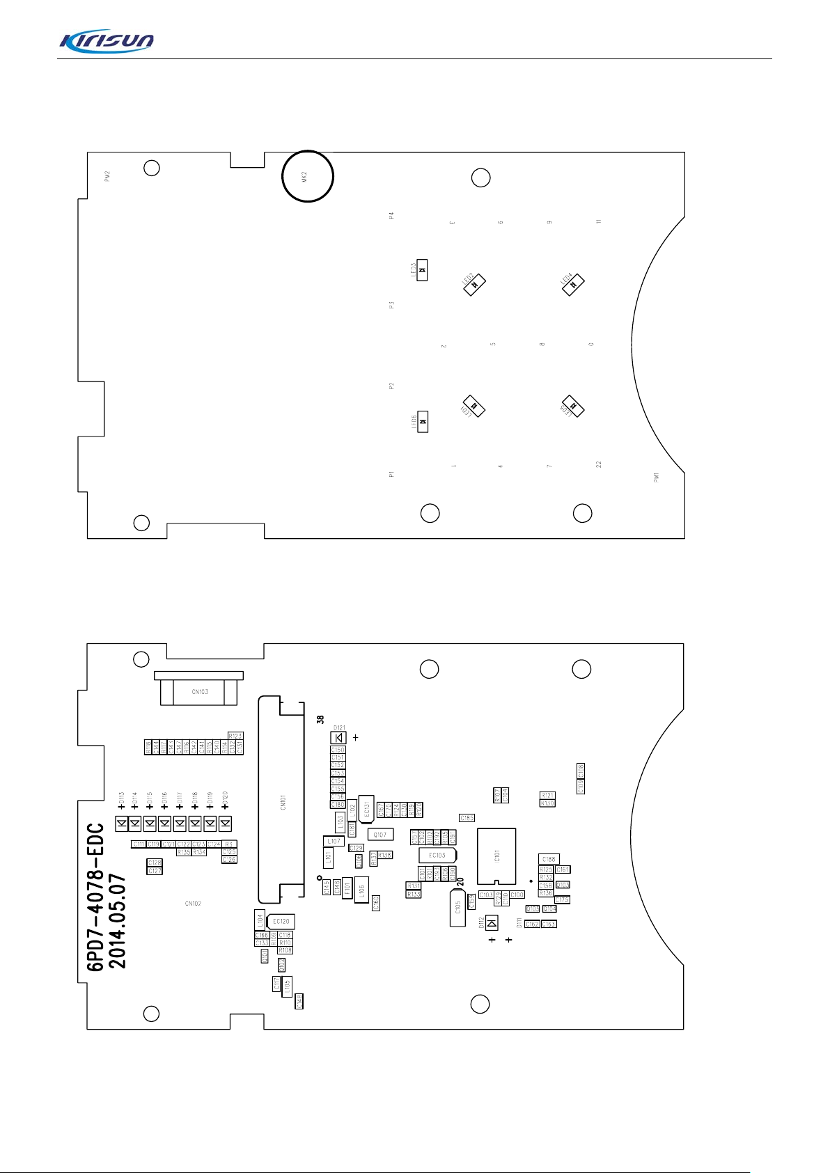
Figure 3 TP660 keypad Top Side PCB View
TP660 Service Manual
Figure 4 TP660 keypad Bottom Side PCB View
Page 52 of 65
Page 56

Figure 5 TP660 Mainboard Schematic Diagram(400-470MHz)
TP660 Service Manual
QT_DQT_IN
CN101
CON38
R131
220K
R132
C105
102
4039
1
2
3
4
5
6
7
8
9
10
11
12
13
14
15
16
17
18
19
20
21
22
23
24
25
26
27
28
29
30
31
32
33
34
35
36
37
38
C128 220P
10K
14
U101-D
C141
103
R145
270K
C152
C153
C154
C155
100P
100P
100P
100P
C161
C162
C163
103
103
103
13
12
C156
100P
L104
BLM21PG221S
21
R142
3K3
C142
103
C143
682
C158
C157
100P
100P
L105
BLM18AG601S
R130
82K
10
R144
470K
C159
100P
MSW
MODE1
MODE2
SELECT
SWB+
C127
393
7
R143
12K
U102-C
9
TP103
USB_D-
USB_D+
1
BOOT_CRL
EXT_PTT
LCD_CS1
LCD_SLK
LCD_SLD
LCD_RES
LCD_A0
K1
K2
K3
K4
K5
K6
K7
K8
MIC_5V
RSSI
VOL_OUT
3V3
LAMP
100P
R129
100K
U102-B
8
5R_A
TP102
1
BLM18AG601S
BLM18AG601S
C100
C126
103
R128
R133
100K
100K
10
8
9
C125
U101-C
C139
183
5
102
R139
R140
5K6
5K6
6
C140
R141
822
1M
R148
22K
C144
C145
103
103
R146
390K
R147
220K
USB_D+
USB_D-
L111
L110
MIC_IN
C101
470P
U102-D
12
13
2T/5T
1
2
3
Hole
H9
C124
123
5
7
6
U101-B
C138
14
C132
105
R150
10K
9
U102-A
105
C149
105
8
7
6
54
3
1
2
R138
150K
R137
68K
C136
5R_A
105
R155
470K
Q104
2SK1824
D
2S3
G
1
R153
1K
FM_MUTE
9
1
2
3
Hole
H10
R126
R127
180K
C123
222
R136
470K
R135
C134
10K
105
C146
105
R154
100K
8
7
6
54
R125
180K
22K
C122
683
C137
105
R134
U102-E
18K
NJM2902V
4
11
R149
1K
1
2
3
Hole
H11
C147
47P
R124
150K
2
1
3
U101-A
C120
105
AF_OUT
5R_A
C133
104
VOL_IN
BAT7V5
L102
BLM18AG601S
C190
105
VOX
9
8
7
6
54
C121
R123
33K
105
R121
100K
C191
MICPOW_SW
MIC_OUT
U105
XC6204B502MR
1
VIN
2
VSS
3
CE
103
EC151
2.2uF/10V
OUT
NC
+
4
11
U101-E
NJM2902V
C102
103
VOX
C115
104
C106
102
5
4
R122
C119
47K
105
AF PROCESS CIRCUIT
AF_OUT
5R_A
C148
10U/10V
C135
C117
104
104
5
C171
682
C170
682
C160
R157
104
2K2
MIC_5V
C104
C130
104
10U/10V
R113
100K
R117 10K
R118
100K
R114
100K
C114
105
D101
1SS372
C129
105
U104
UMC4N
D115
1SS372
C165
470P
C164
470P
D114
1SS372
C172
470P
AOUT2A-IN3A+IN4GND B+IN
1
C113 470P
C166
470P
7V+8
BOUT
34
2
1
+
+
C108 100P
R112
470K
5
6
B-IN
R116
820K
EC168
EC167
U103
NJM2100V
R156
R152
820R
2K7
1uF/16V
1uF/16V
5R
L101
BLM18AG601S
C118
105
FM_SW
Q10
5
2SA1586
23
1
Q103
2SC4116
R160
0R
C107
R111
223
22K
10K
R151
223
C150
TP101
MIC
1
C112
R115
223
10K
MIC_IN
9
1
2
3
45
Hole
H1
1
8
2
3
7
6
9
8
7
6
54
Hole
H2
9
1
2
3
45
Hole
H3
1
8
2
7
3
6
Hole
H4
9
8
7
6
54
9
1
2
3
8
7
6
54
Hole
H5
9
1
2
3
45
8
7
6
Hole
H6
9
1
2
3
8
7
6
54
Hole
H7
9
1
2
3
8
7
6
54
Hole
H8
Page 53 of 65
Page 57

TP660 Service Manual
C291
10U/10V
C290
A3V3
C278
103
C269
105
C279
105
C270
103
C281
C282
C271
105
C283
103
105
C273
104
C272
103
10U/10V
R235
NC
105
3V3
C276
104
103
C236
C274
104
C234
NC
C284
103
L208
BLM18AG601S
L202
BLM18AG601S
C235
104
3V3
C310
C239
104
L203
47uH
R234
10K
A3V3
104
R233
10K
1
HPVCC
9
CDC_AVCC
12
PLL_VDD33
66
ADC_AVDD33_Q
67
ADC_AVDD33_I
76
DAC_AVDD33
79
DCDC_VDD33
32
VDD12
53
VDD12
69
ADC_AVDD12_I
64
ADC_AVDD12_Q
77
DCDC_VDD12
80
DCDC_SW
18
BCLK
17
LRCK
16
MCLK
19
ADCDAT
39
RESETN
45
DBIST_IN
38
TEST_MODE
103
C238 105
2T/5T/DTMF_OUT
MIC_OUT
54
46
20
5
11
6
MIC1_P8MIC2_P
MIC1_N7MIC2_N
DACDAT
MICBIAS
DBIST_OUT
U201
HR_C5000
VSS1233VSS1252VSS123HPGND13PLL_VSS3365ADC_AGND_Q68ADC_AGND_I73DAC_AVSS3378DCDC_VSS41V_SDI42V_SDO43V_SCLK44V_CS59RF_RX_EN60RF_TX_EN61ADC_VBG_Q14XTAL15CLKOUT62ADC_QVINN63ADC_QVINP
21
C237
C240
C5000_RST
C311
104
104
DMR_SLEEP
22
23
24
25
26
27
28
29
30
31
47
RTS
PWD
VDD3340VDD33
TX_RDY
STDBY_ENB
V_SDI
V_SDO
MCBSP_FSX
MCBSP_TXD
MCBSP_FSR
MCBSP_RXD
MCBSP_CLKX
MCBSP_CLKR
PKT_RX_WAKE
C230
104
V_CS
V_SCLK
R231
10K
DAC_IVOUT
DAC_QVOUT
LINEOUT
ADC_VBG_I
HPOUT
U_CS
U_SCLK
U_SDI
U_SDO
RF_RX_INTER
RF_TX_INTER
SYS_INTER
TIME_SLOT_INTER
C_CS
C_SCLK
C_SDO
C_SDI
ADC_IVINP
ADC_IVINN
CDC_VREF
3V3
R232
10K
C231
10P
75
74
10
72
2
58
57
56
55
51
50
49
48
37
36
35
34
70
71
4
R229
10R
102 C233
C225 104
C226 104
C232
104
C227
103
R225 1K
4
3
C228
10U/10V
29.4912MHz
VCC
OUT
R238
1K
R236
1K
DMR_CS
DMR_SCLK
DMR_SDI
DMR_SDO
RF_RX_INTER
RF_TX_INTER
SYS_INTER
TIME_SLOT_INTER
I2S_FS
I2S_CK
I2S_TX
I2S_RX
IF_OUT
X201
NC
GND
C241
220P
1
2
C244
220P
ADC_IN_N
R227
MOD_Q
DMR_VCC
MOD_I
C252
104
R243
220K
C224
105
C248
R244
102
100K
3V3
R226
NC
NC
R240
10K
1
2
3
C249
105
U203
TC75S51F
1
-V
344
R241
15K
+V
C253
470P
5
C250
R253
105
1K
VOL_IN
VOL_OUT
C257
SWB+
R258
VOL_IN
2K2
103
1
2
3
VOL-SWITCH
SW401
R263
100R
R249
NC
4
5
Q206
DTC144EE
BAT+
C256
102
VOL_MAX
Page 54 of 65
Page 58

3V3
EXT_PTT
MSW
R312
47K
SW301
ALARM-KEY
C314
102
RX_LED TX_LED
2T/5T/DTMF_OUT
VOL_IN
R314
180R
LED301
GREEN
Q301
DTC144EE
W/N_SW
LED302
C346
104
FM_SW
BAT+
LED303
GREEN
R341
2K2
RED
ALARM_KEY
VCOVCC_SW
R313
10K
C352
105
CTC/DCS_OUT
R315
220R
DTC144EE
VOL_MAX
R370
1K
R358 1K
R357
MODE2
DMR_SW
FM_MUTE
BUSY
RSSI
RF_APC_SW
POW_C
POW_DET
MOD2_BIAS
APC/TV
QT_DQT_IN
C337
105
C315
102
Q302
TP660 Service Manual
PLL_CLK
PLL_CS
PLL_DAT
DMR_SDI
PLL_LD
DMR_SCLK
DMR_SDO
DMR_CS
3V3
R360
10K
54
R310
R311
100K
10K
1K
69
68
ECN3
48
ECN2
47
ECN1
46
ECN0
45
44
PTT_KEY
43
42
41
40
39
38
37
36
5TC
VOX
35
34
33
32
31
30
29
26
25
72
1
TP304
JTAG_SWDIO
R339
R340
4K7
22K
C335
C336
183
R336
22K
C333
183
PB1251PB1352PB1453PB15
PA10
PA9
PB11
PB10
PE15
PE14
PE13
PE12
PE11
PE10
PE9
PE8
PE7
PB2
PB1
PB0
PC5
PC4
PA7
PA6
PA5
PA4
PA3
PA2
PA13
BEEP
5RC
SAVE
R338
4K7
392
R335
15K
C332
153
R316
47K
1234
SW302
CODE-SWITCH
5
6
PD855PD9
FAST_LOCK
56
FL_C
R317
47K
C316
103
LCD_RES
PD1057PD1158PD1259PD1360PD14
STM32F405VGT6
MANDOWN
BATT
2T/5T
C302
8P
R318
47K
C317
103
R309 1K
R350 NC
LCD_A0
RF_RX_INTER
LCD_CS1
R308 1K
61
U301
RF_TX_INTER
104
C360
49
VSS_274VSS_510VSS_427VSS_3
VCAP_1
SYS_INTER
TIME_SLOT_INTER
R319
47K
C318
103
C343
105
C345
103
C344
105
3V3
C307
C305
C306
C308
C312
VCC
OUT
HOLDN
105
R307
NC
C338
104
PST9124
VCC
WPN
VEE1
VEE2
U303
8
7
3
4
C313
103
103
I2S_FS
I2S_CK
I2S_RX
I2S_TX
K2
K3
K4
K5
K6
K7
K8
V_CS
V_SCLK
V_SDO
V_SDI
SELECT
MODE1
K0
K1
USB_DUSB_D+
1
NC
2
3
R320 0R
R321 10K
3V3
MICPOW_SW
3V3
3V3
R305
10K
R306
10K
FAST_LOCK
C320
104
TP303
BOOT0
BOOT_CRL
1
R328
R327
NC
NC
C325
C326
NC
NC
104
104
104
99
22
21
19
100
75
6
VDD
RX_LED
FLASH_SDI
TX_LED
VDD_150VDD_511VDD_428VDD_3
FLASH_SDO
FLASH_CS
FLASH_SCK
K
1
R355
R356 1K
LCD_SLK
LCD_SLD
TP305
JTAG_RESET
VDD_2
1
VBAT
PE614NRST1PE22PE33PE44PE57PC13_ANTI_TAMP8PC14_OSC32_IN9PC15_OSC32_OUT12OSC_IN13OSC_OUT73VCAP_215PC016PC117PC218PC320VREF-23PA0_WKUP24PA162PD1563PC664PC765PC866PC967PA8
DMR_SLEEP
C339
VDDA
VREF+
104
C361
LAMP
R301 1K
TP301
JTAG_SWCLK
1
R391 1K
76
PA14
77
PA15
78
PC10
79
PC11
80
PC12
81
PD0
82
PD1
83
PD2
84
PD3
85
PD4
86
PD5
87
PD6
88
PD7
89
PB3
90
PB4
91
PB5
92
PB6
93
PB7
94
BOOT0
95
PB8
PB9
PE0
PE1
PA11
PA12
5
R361
10K
103
SCL
96
SDA
97
98
70
71
R342
10K
5
4
R334
0R
13
X301
C303
8MHz
8P
C5000_RST
3V3
U302
ECN0
ECN1
ECN2
ECN3
C319
103
FLASH_CS
FLASH_SDO
FLASH_SCK
FLASH_SDI
W25Q80BVSIG
1
CSN
2
SO
6
SCK
5
SI VSS
FPC301
3V3
MANDOWN
C370
5C
NC
SDA
SCL
1
2
3
R330
NC
7
6
5
4
3
2
1
C342
R362
4K7
L303
NC
U305
NC
1
-V
344
R329
NC
NC
+V
R332 1K
R353 1K
R352 1K
R351 1K
3V3
C340
R345
R363
4K7
HR_V3000S
4
SDA
3
SCL
2
GND
5
K2
K1
K0
PTT_KEY
R354
C350
47K
104
C341
4
3
2
1
NC
FL
VDA DOUTX
GND
VREF
DOUTY
TOUT
U304
NC
C362
104
C327
NC
103
R346
R343
NC
5
6
7
SCK
8
VDD
C331
NC
1
I/O VCC
2
I/O
3
GND
NC
R344
NC
C369
NC
5
4
FL_C
SW
U306
NC
105
NC
3V3
U307
6
VDD
5
VPP
1
RSTO
C328
C324
NC
R331
NC
Page 55 of 65
Page 59

POWER CIRCUT
TP660 Service Manual
J401
BATTERY-CON
+
-
2K2
DTC144EE
10uF/10V
BAT7V5
R401
+
C410
C406
104
102
C409
22uF/10V
Q402
C428
104
5C
+
C435
104
5T
C438
104
EC431
10uF/10V
C432
104
5R
R422
10K
D403
MA2S111
D404
MA2S111
R420
NC
200K
R419
10K
R418
100K
C422
103
BATT
C405
R402
100K
104
POW_C
SWB+
POW_DET
R408
47K
BATT
BAT+
F401
1
2
3
3AFUSE
21
C401
47P
1SR154-400
C404
100P
D402
12
BAT7V5
C419
105
C415
105
+
C407
104
EC403
10uF/16V
U404
XC6204B502MR
1
VIN
OUT
2
C412
105
VSS
3
CE
C439
103
U403
XC6204B502MR
1
VIN
2
VSS
3
CE
C440
103
U402
XC6204B502MR
1
VIN
2
VSS
3
CE
C442
470P
NC
OUT
NC
OUT
NC
Q401
FMMT717
R405
47K
5
4
SAVE
5
C433
103
4
5RC
5
C436
103
4
5TC
R406
C430
103
+
EC434
C437
2.2U/10V
L401
BLM18AG601S
4
EN
R412
2
C441
22U/10V
+
C445
105
4K7
C416
104
GND
U401
LN8259
C408
223
BS15IN
6
SW
3
FB
L404
10uH
C424
103
D405
XBS104S13R-G
R425
22K
TP401
R410
68K
R411
1K5
3V3
1
3V3
C413
+
C427
104
103
C425
22U/10V
Page 56 of 65
Page 60

W/N_SW
BUSY
C534
TP660 Service Manual
5T
J501
1
C507
C505
120P
2P
L504
3T
C506
2P
C509
NC
0.39R
R559
0.39R
R560
0.39R
C721
47P
5R
C520
C521
470P
104
C517
C512
102
RB706F
D512
C516
C568
6P
Q504
2SC3356
C548
104
FD501
C24450
R555
1.8K
15
16
MIXI
GND
XIN2XOUT3MIXOUT4VCC5IFI6DEC7FILO8FILI AF
1
2
OUT
C569
NC
RX_VCO
C544
C550
120P
14
NREC
C571
R545
104
1K
R546
6K8
Q503
2SC3356
R547
4K7
R548
22R
R518
103
100R
C543
12P
12
R522
1.8K
9
10
11
12
13
C555
102
IFO
RSSI
NDET
QUAD
C554
470P
R527
330K
C553
470P
C552
104
C572
470P
L519
22nH
C574
12P
C575
NC
C573
470P
C577
104
C547
104
XF501
49.95MHz
4
3
215
6
C542
12P
C559
104
450_IF
R523
4K7
C556
223
R525
R524
180K
27K
R526
3K3
Q502
RD01MUS2
L521
1uH
R551
1K5
12
L522
R549
R550
47K
C578
470P
5R
AF_OUT
10K
RX_VCO
BLM18AG601S
R517
100R
C541
NC
BLM21PG221S
C716
10P
L528
21
C537
C538
103
470P
C540
103
C710
105
C709
104
C580
L520
0R
C579
33P
C582
C583
470P
104
L533
22nH
C717
NC
R516
47R
L514
R515
470nH
2K2
L513
560nH
C539
DMR_VCC
C711
R531
470R
102
R530
1K
R529
750K
Q509
2SC3356
L523
100P
2.7nH
C581
NC
C585
103
C530
6P
L515
27nH
C531
20P
C536
103
R510
100K
R511
56K
7P
Q506
3SK318
R512
C535
180R
103
U503
UMC4N
5
C713
103
IF_OUT
Q501
RD07MUS2B
C588
L531
23
R553
82K
NC
C704
470P
1
1
5R
BLM18AG601S
C528
3P
12
L524
8T
2
2
1
1
L525
BLM21PG221S
D523
R599
100K
R504
100K
C712
105
DMR_SW
C586
47P
C598
470P
R570
2K2
R701
27K
C560
470P
L512
4T
D508
1
R554
47R
R552
33K
C584
102
C533
470P
APC/TV
R513
100K
R514
56K
C529
100P
TP1
RX
TP501
RX
34
2
1
C587
15P
C597
103
C705
C527
2P
HVC350B
C589
C590
15P
C596
104
R571
100R
473
C706
R574
22K
R503
100K
L511
4T
D507
HVC350B
C591
27P
6P
15P
5T
+
C599
22uF/10V
C532
103
8
27K
R569
103
R572
NC
7
6
5
C707
470P
C561
470P
R581
100K
C524
2P
L530
4T
C526
6P
D513
HVC350B
R543
22R
R540
2K2
R541
2K2
C566
470P
DTC144EE
R535 1K
RSSI
R533 1K
5R
R528
10R
103
C570
470P
C722
C723
105
470P
R537
15R
R536
8K2
LO
C546
103
Q510
C549
C557
+
103
EC558
10uF/10V
ELFY450H
R538
8K2
MA2S077
D511
MA2S077
223
CF501
C564
D510
C724
103
R542
9P
R520
Q507
2SC3356
C551
104
1K
1K
Q511
DTA143ZETL
C545
33P
2ND_LO
1
IN
GND3GND
4
R539
R588
4K7
R521
470R
GT3136
L518
22nH
22K
R519
560K
U501
L526
2T
C595
V+
BOUT
B-IN
B+IN GND
U502
NJM2904V
C593
D501
68P
HVU131
C592
12P
L527
220nH
R556
390R
R595
390R
104
5
U505
UMC4N
R568
270R
1
AOUT
2
A-IN
3
A+IN
4
L509
82nH
C525
100P
C513
8P
R598
22R
1
2
34
C708 56P
R567
1M5
R702
150K
C519 47P
C
E1
E2
R507
22R
C594
102
C
E1
E2
Q505
AT41511
C508
NC
R700
1M5
C523
102
B
RF_APC_SW
BAT+
R562
150K
R564
150K
R566
150K
R575
5K6
B
R506
6K8
L505
3T
R561
C720
102
R508
330R
R505
5K6
C518
33P
L508
22nH
C503
1P5
L503
4T
C504
6P
D504
MA2S077
C718
C719
103
470P
BAT+
R502
100K
5P
L507
4T
4P
D506
HVC350B
C501
3P
L502
3T
C502
C500
4P
D503
MA2S077
C563
C562
470P
470P
R501
100K
C515
3P
L506
4T
D505
HVC350B
Page 57 of 65
ANTENNA
1
1
TP502
ANT
L501
1uH
NC
C514
4P
1
TP503
GND
C510
4P
Page 61

TP660 Service Manual
PLL_LD
PLL_DAT
PLL_CLK
PLL_CS
PLL3V3
+
R642 100R
R643 100R
R629 100R
PLL3V3
R627
100R
C638
104
MOD_Q
CTC/DCS_OUT
MOD2_BIAS
U601
SKY72310
5C
C667
C666
105
470P
L603
BLM18AG601S
R609
10R
10K
R632
C669
470P
5
19NC7
24
VDD
MUX
C-C
FVCO
VC P
NC
NC
/FVCO
NC
GND
XTALOUT8/OSC
18NC12
C649
102
C644
103
L608
470nH
C645
180P
C683
C682
105
104
8
AOUT
V+
7
A-IN
BOUT
6
A+IN
B-IN
5
B+IN GND
U603
NJM2904V
R648
18K
C677
183
U602
XC6204B332MR
5
1
OUT
VIN
C665
104
R634
10R
R630
10R
C662
470P
C664
4.7U/10V
R628
C656
C657
C655
100P
100P
103
L601
3.3uH
3
4
C639
VCC
102
X601
16.8MHz
GND OUT
1VC2
C640
332
100K
R641
560K
R605
15K
VSS
4
CE
NC
C663
104
1K
C658
100P
C635
10P
C636
10P
C695
NC
C678
100P
2
3
C637
104
R631
10K
1
11
23
MOD
C-C
VC EL
VCC-XTAL
13
NC
4
PS
20
DATA
22
CLK
21
/CS CPOUT
OSC
9
17NC10
C634
470P
R638
10K
C643
L607
47P
560nH
R639
330K
Q605
2SC5066(Y)
R646
4K7
R655
0R
R644
100K
R615
22K
C686
153
PLL&VCO Circuit
5C
2
15
16
3
14
6
R640
470R
C646
103
BLM18AG601S
R651
100K
1
2
3
4
+
EC668
10uF/10V
C654
103
C676
104
C693
470P
C650
104
C689
L602
18nH
C660
6P
C659
100P
R635
47R
+
NC
R660
5R
C648
68P
L609
330nH
C647
33P
5C
L610
R652
10K
C681
100P
C680
R649
105
9K1
2P
R636
56R
EC651
FL
R650 100KR645
R658
470R
C661
R637
10K
2.2uF/10V
C688
L630
BLM18AG601S
C685
105
R659
100K
6P
Q608
2SC5066(Y)
TP601
CV
1
L600
BLM18AG601S
C652
104
2ND_LO
NC
C692
105
MOD_VCO
C687
332
MOD_I
C670
470P
MOD_VCO
C653
470P
FVCO
L611
390nH
L619
390nH
D601
MA2S111
R623
4K7
EC671
10uF/10V
D606
VCOVCC_SW
1SV305
VCOVCC
D604
Q606
2SC4617(S)
C673
470P
+
C672
103
R620
4K7
D610
1SV278
D609
1SV305
D608
1SV305
D607
1SV305
1SV305
1SV305
D605
1SV305
VCOVCC
C675
C674
103
105
R621
150K
R622
68K
L612
33nH
34
2
1
D603
D602
1SV305
U604
UMC4N
L620
33nH
C608
0P5
C609
0P5
C601
12P
L613
10nH
C620
10P
C603
RXVCO_VCC
5
C627
104
L621
15nH
Q607
2SJ243
RXVCO_VCC
C611
C610
R602
4K7
104
470P
C604
12P
C605
18P
C606
10P
NC
VCOVCC_SW:T:0V;R:3.3V
C628
R612
4K7
470P
C623
8P
C624
18P
C622
NC
C625
15P
R601
5K6
C612
C613
104
470P
R604
L616
100R
390nH
L615
390nH
C614
1P5
Q601
2SC3356
R603
C607
C626
120R
39P
L614
390nH
FVCO
R611
5K6
L623
390nH
L622
390nH
47P
R614
100R
Q603
2SC3356
C629
470P
R613
120R
L624
390nH
C690
104
C632
6P
C617
1P5
C630
104
C631
1P5
R608
1K
C616
470P
L617
33nH
R606
220K
2SC5066(Y)
C615
C619
470P
Q602
LO
R619
470R
104
C684
470P
L625
33nH
R616
5K6
R610
NC
C618
6P
R617
3K9
R680
1K
C700
7P
Q604
2SC5066(Y)
C633
8P
C699
3P
L626
12nH
C698
9P
Page 58 of 65
Page 62

Figure 6 TP660 Mainboard Schematic Diagram(136-174MHz)
TP660 Service Manual
QT_DQT_IN
CON38
CN101
R131
220K
C128 220P
R132
10K
14
C105
102
4039
1
2
3
4
5
6
7
8
9
10
11
12
13
14
15
16
17
18
19
20
21
22
23
24
25
26
27
28
29
30
31
32
33
34
35
36
37
38
U101-D
C141
103
R145
270K
C152
C153
C154
C155
100P
100P
100P
100P
C161
C162
C163
103
103
103
13
12
C156
100P
L104
BLM21PG221S
21
MIC_IN
MSW
MODE1
MODE2
SELECT
R142
3K3
C142
103
C143
103
C158
C157
100P
100P
L105
BLM18AG601S
SWB+
LAMP
R130
R129
82K
100K
C127
393
7
R143
12K
U102-C
10
9
R144
470K
TP103
TP102
USB_D-
USB_D+
1
C159
100P
BOOT_CRL
EXT_PTT
LCD_CS1
LCD_SLK
LCD_SLD
LCD_RES
LCD_A0
K1
K2
K3
K4
K5
K6
K7
K8
MIC_5V
RSSI
VOL_OUT
3V3
1
U102-B
8
5R_A
5
6
8
C139
183
C144
103
USB_D+
USB_D-
C126
103
R133
100K
10
9
C125
U101-C
R146
390K
102
R140
5K6
C140
R141
822
1M
C145
103
R147
220K
1
2
3
45
Hole
H9
C124
123
R126
R127
R128
100K
7
U101-B
C138
R139
105
5K6
R148
22K
U102-D
12
14
13
C132
105
R150
10K
2T/5T
9
8
1
2
7
3
6
U102-A
1
R138
150K
5R_A
R155
470K
C149
105
9
Hole
H10
5
6
Q104
2SK1824
D
R153
1K
180K
C123
222
3
2
R137
68K
C136
105
8
7
6
54
R136
470K
R135
C134
10K
105
C146
105
2S3
G
1
R154
100K
FM_MUTE
1
2
3
R125
180K
22K
C122
683
C137
105
R134
U102-E
18K
NJM2902V
4
11
R149
1K
9
8
7
6
54
Hole
H11
AF_OUT
VOL_IN
BAT7V5
1
5R_A
C133
104
L102
BLM18AG601S
C147
47P
R124
150K
2
3
U101-A
R122
C120
105
C190
105
VOX
C121
R123
33K
105
R121
100K
MIC_OUT
XC6204B502MR
1
VIN
2
VSS
3
CE
C191
103
EC151
2.2uF/10V
4
11
U101-E
NJM2902V
C106
470P
U105
5
OUT
4
NC
C102
103
VOX
C115
+
104
C119
47K
105
MICPOW_SW
AF PROCESS CIRCUIT
AF_OUT
5R_A
C148
10U/10V
C135
C117
104
104
5
C171
104
C170
104
C160
R157
104
560R
MIC_5V
C104
C130
R113
100K
C129
105
R117 10K
10U/10V
R118
100K
104
R114
100K
C114
105
D101
1SS372
U104
UMC4N
D115
1SS372
C165
470P
C164
470P
D114
1SS372
C172
470P
AOUT2A-IN3A+IN4GND B+IN
1
C113 470P
C166
470P
C108 220P
6
7V+8
B-IN
BOUT
R116
820K
34
2
1
5
+
+
R112
330K
NJM2100V
5R
L101
BLM18AG601S
C118
105
FM_SW
R156
2K7
Q105
2SA1586
EC168
1uF/16V
EC167
1uF/16V
R152
Q103
820R
2SC4116
R160
0R
C107
R111
223
22K
10K
R151
223
C150
U103
R115
10K
TP101
MIC
1
C112
223
MIC_IN
9
1
2
3
8
7
6
54
Hole
H1
9
1
2
3
8
7
6
54
Hole
H2
9
1
2
3
45
Hole
H3
1
8
2
3
7
6
Hole
H4
9
8
7
6
54
9
1
2
3
45
8
7
6
Hole
H5
9
1
2
3
Hole
H6
9
1
8
2
3
7
6
54
8
7
6
54
Hole
H7
9
1
2
3
45
8
7
6
Hole
H8
Page 59 of 65
Page 63

TP660 Service Manual
C291
10U/10V
C290
A3V3
C279
C276
104
C278
103
103
C269
105
C281
C282
C271
105
C283
103
105
C273
104
C272
103
10U/10V
R235
NC
105
105
C270
103
3V3
C236
C274
104
C284
103
C234
NC
L208
BLM18AG601S
L202
BLM18AG601S
C235
104
3V3
C310
C239
104
L203
47uH
R234
10K
C5000_RST
A3V3
104
R233
10K
1
HPVCC
9
CDC_AVCC
12
PLL_VDD33
66
ADC_AVDD33_Q
67
ADC_AVDD33_I
76
DAC_AVDD33
79
DCDC_VDD33
32
VDD12
53
VDD12
69
ADC_AVDD12_I
64
ADC_AVDD12_Q
77
DCDC_VDD12
80
DCDC_SW
18
BCLK
17
LRCK
16
MCLK
19
ADCDAT
39
RESETN
45
DBIST_IN
38
TEST_MODE
103
C238 105
2T/5T/DTMF_OUT
MIC_OUT
54
46
20
5
11
6
MIC1_P8MIC2_P
MIC1_N7MIC2_N
DACDAT
MICBIAS
DBIST_OUT
U201
HR_C5000
VSS1233VSS1252VSS123HPGND13PLL_VSS3365ADC_AGND_Q68ADC_AGND_I73DAC_AVSS3378DCDC_VSS41V_SDI42V_SDO43V_SCLK44V_CS59RF_RX_EN60RF_TX_EN61ADC_VBG_Q14XTAL15CLKOUT62ADC_QVINN63ADC_QVINP
21
C237
C240
C311
104
104
DMR_SLEEP
22
23
24
25
26
27
28
29
30
31
47
RTS
PWD
VDD3340VDD33
TX_RDY
V_SDI
STDBY_ENB
V_SDO
MCBSP_FSX
MCBSP_TXD
MCBSP_FSR
MCBSP_RXD
MCBSP_CLKX
MCBSP_CLKR
10K
DAC_IVOUT
DAC_QVOUT
LINEOUT
ADC_VBG_I
HPOUT
U_CS
U_SCLK
U_SDI
U_SDO
RF_RX_INTER
RF_TX_INTER
SYS_INTER
TIME_SLOT_INTER
C_CS
C_SCLK
C_SDO
C_SDI
ADC_IVINP
ADC_IVINN
CDC_VREF
3V3
R232
10K
C231
10P
75
74
10
72
2
58
57
56
55
51
50
49
48
37
36
35
34
70
71
4
R229
10R
102 C233
C232
C225 104
C226 104
C227
103
104
R225 1K
PKT_RX_WAKE
C230
104
V_CS
V_SCLK
R231
4
3
C228
10U/10V
29.4912MHz
VCC
OUT
R238
1K
R236
1K
DMR_CS
DMR_SCLK
DMR_SDI
DMR_SDO
RF_RX_INTER
RF_TX_INTER
SYS_INTER
TIME_SLOT_INTER
I2S_FS
I2S_CK
I2S_TX
I2S_RX
IF_OUT
X201
NC
GND
C241
220P
1
2
C244
220P
ADC_IN_N
R227
MOD_Q
DMR_VCC
MOD_I
C252
104
R243
220K
C224
105
C248
R244
102
100K
3V3
R226
NC
NC
R240
10K
1
1
2
-V
3
344
C249
105
U203
TC75S51F
R241
47K
+V
C253
470P
5
C250
R253
105
1K
VOL_IN
VOL_OUT
C257
SW401
R258
VOL_IN
2K2
103
VOL-SWITCH
1
2
345
R263
R249
NC
SWB+
BAT+
Q206
0R
DTC144EE
C256
102
VOL_MAX
Page 60 of 65
Page 64
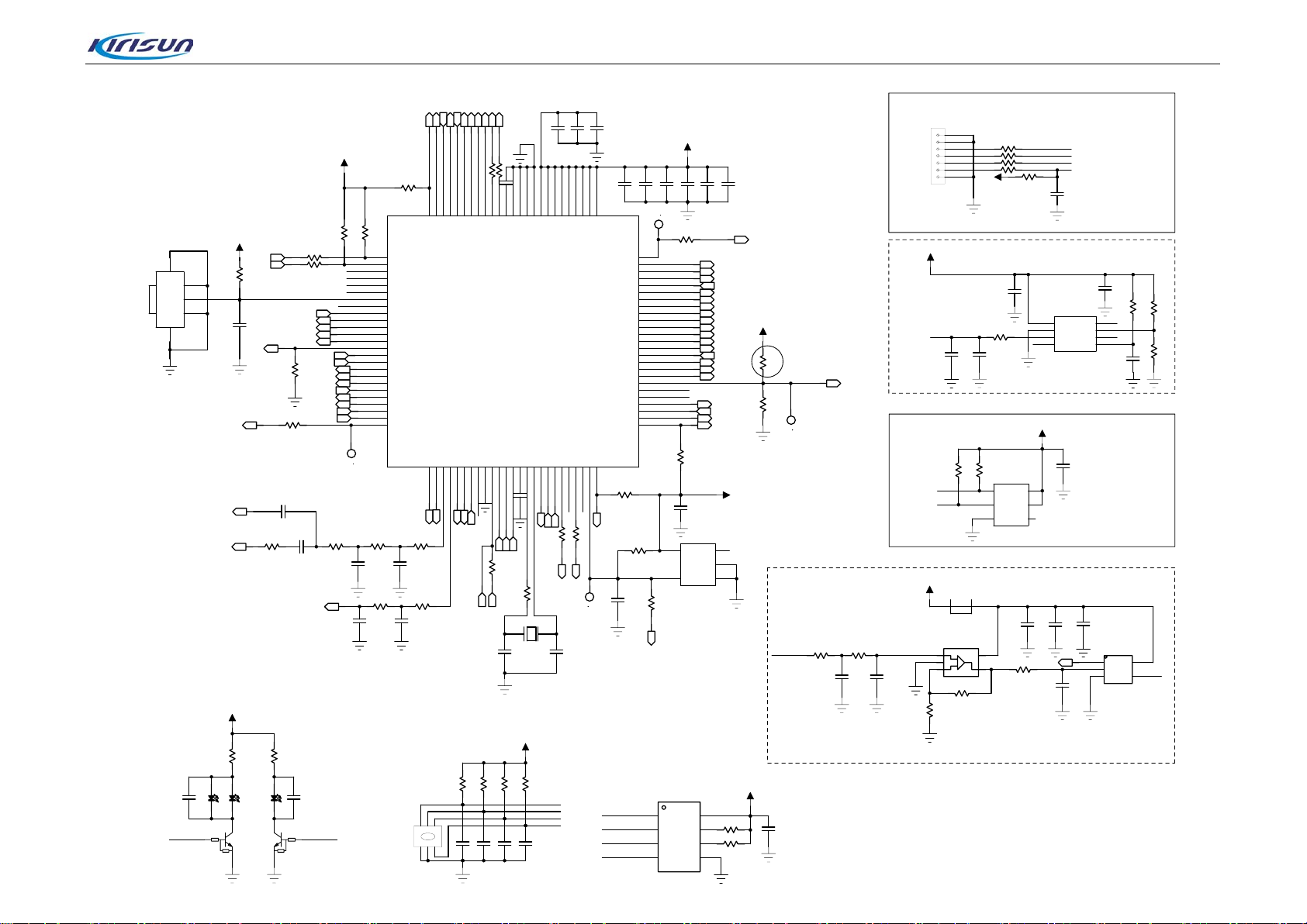
SW301
ALARM-KEY
2T/5T/DTMF_OUT
VOL_IN
R312
47K
W/N_SW
C346
BAT+
TP660 Service Manual
PLL_CLK
PLL_CS
PLL_DAT
DMR_SDI
PLL_LD
DMR_SCLK
DMR_SDO
DMR_CS
3V3
R360
10K
54
R310
R311
100K
RF_APC_SW
POW_C
POW_DET
MOD2_BIAS
APC/TV
QT_DQT_IN
BUSY
10K
1K
69
68
ECN3
48
ECN2
47
ECN1
46
ECN0
45
44
PTT_KEY
43
42
41
40
39
38
37
RSSI
5TC
VOX
R340
36
35
34
33
32
31
30
29
26
25
72
1
TP304
JTAG_SWDIO
R339
4K7
22K
C335
C336
392
183
R336
22K
C333
183
3V3
104
FM_SW
EXT_PTT
MSW
R341
2K2
ALARM_KEY
VCOVCC_SW
R313
10K
C352
105
CTC/DCS_OUT
VOL_MAX
FM_MUTE
R370
1K
R358 1K
R357
MODE2
DMR_SW
C337
105
PB1251PB1352PB1453PB15
PA10
PA9
PB11
PB10
PE15
PE14
PE13
PE12
PE11
PE10
PE9
PE8
PE7
PB2
PB1
PB0
PC5
PC4
PA7
PA6
PA5
PA4
PA3
PA2
PA13
BEEP
5RC
SAVE
R338
4K7
R335
15K
C332
153
56
PD855PD9
FAST_LOCK
PD1057PD1158PD1259PD1360PD14
FL_C
BATT
LCD_RES
R309 1K
STM32F405VGT6
MANDOWN
R350 NC
2T/5T
C302
8P
LCD_A0
RF_RX_INTER
LCD_CS1
R308 1K
61
RF_TX_INTER
104
C360
49
VSS_274VSS_510VSS_427VSS_3
VCAP_1
U301
SYS_INTER
TIME_SLOT_INTER
C343
105
C345
103
C344
105
3V3
C307
C305
C306
C308
C312
VCC
OUT
105
R307
NC
C338
104
U303
PST9124
VEE1
VEE2
103
NC
I2S_FS
I2S_CK
I2S_RX
I2S_TX
K2
K3
K4
K5
K6
K7
K8
V_CS
V_SCLK
V_SDO
V_SDI
SELECT
MODE1
K0
K1
USB_DUSB_D+
C313
103
MICPOW_SW
3V3
R305
NC
BOOT_CRL
R306
10K
1
TP303
BOOT0
3V3
1
2
3
R328
R327
NC
NC
FAST_LOCK
C325
C326
NC
NC
104
104
104
99
22
21
19
100
75
6
VDD
VDD_150VDD_511VDD_428VDD_3
FLASH_SDI
FLASH_SDO
FLASH_SCK
TX_LED
R355 1K
LCD_SLD
JTAG_RESET
C303
8P
FLASH_CS
R356 1K
LCD_SLK
TP305
VDD_2
1
VBAT
PE614NRST1PE22PE33PE44PE57PC13_ANTI_TAMP8PC14_OSC32_IN9PC15_OSC32_OUT12OSC_IN13OSC_OUT73VCAP_215PC016PC117PC218PC320VREF-23PA0_WKUP24PA162PD1563PC664PC765PC866PC967PA8
5
DMR_SLEEP
C339
103
VDDA
VREF+
104
C361
LAMP
RX_LED
R301 1K
13
X301
8MHz
BOOT0
R361
10K
PA14
PA15
PC10
PC11
PC12
PD0
PD1
PD2
PD3
PD4
PD5
PD6
PD7
PB3
PB4
PB5
PB6
PB7
PB8
PB9
PE0
PE1
PA11
PA12
JTAG_SWCLK
R342
10K
TP301
1
R391 1K
76
77
78
79
80
81
82
83
84
85
86
87
88
89
90
91
92
93
94
95
SCL
96
SDA
97
98
70
71
5
4
R334
0R
C5000_RST
FPC301
3V3
MANDOWN
C370
NC
SDA
SCL
5C
1
2
3
R330
NC
7
6
5
4
3
2
1
C342
L303
NC
U305
NC
1
-V
344
R329
NC
R332 1K
R353 1K
R352 1K
R351 1K
3V3
C340
105
R345
NC
NC
R362
R363
4K7
4K7
U307
HR_V3000S
4
SDA
VDD
3
SCL
VPP
2
GND
RSTO
C324
NC
5
+V
R331
K2
K1
K0
PTT_KEY
R354
C350
47K
104
C341
103
R346
R343
NC
4
3
2
1
3V3
6
5
1
C328
NC
FL
NC
VDA DOUTX
GND
DOUTY
TOUT
U304
NC
C362
104
C327
NC
VREF
5
6
7
SCK
8
VDD
C331
NC
1
I/O VCC
2
I/O
3
GND
NC
R344
NC
C369
NC
5
4
FL_C
SW
U306
NC
R314
180R
C314
102
RX_LED TX_LED
LED301
Q301
DTC144EE
LED302
GREEN
GREEN
R315
220R
C315
102
RED
LED303
Q302
DTC144EE
SW302
CODE-SWITCH
1234
6
3V3
R316
R317
R318
47K
5
R319
47K
47K
47K
ECN0
ECN1
ECN2
C316
C317
103
103
ECN3
C318
C319
103
103
FLASH_CS
FLASH_SDO
FLASH_SCK
FLASH_SDI
W25Q80BVSIG
1
CSN
2
SO
6
SCK
5
SI VSS
U302
VCC
HOLDN
WPN
8
7
R320 0R
3
R321 10K
4
3V3
C320
104
Page 61 of 65
Page 65

POWER CIRCUT
TP660 Service Manual
J401
BATTERY-CON
+
-
2K2
Q402
DTC144EE
10uF/10V
5T
BAT7V5
R401
+
C410
C406
104
102
C409
22uF/10V
C428
104
5C
+
C435
104
C438
104
EC431
10uF/10V
C432
104
5R
R422
10K
D403
MA2S111
D404
MA2S111
R420
NC
200K
R419
10K
R418
100K
C422
103
BATT
C405
R402
100K
104
POW_C
SWB+
POW_DET
R408
47K
BATT
BAT+
F401
1
2
3
3AFUSE
21
C401
470P
D402
1SR154-400
BAT7V5
C404
102
12
C419
105
C415
105
+
C407
104
EC403
10uF/16V
U404
XC6204B502MR
1
VIN
OUT
2
C412
105
VSS
3
CE
C439
103
U403
XC6204B502MR
1
VIN
2
VSS
3
CE
C440
103
U402
XC6204B502MR
1
VIN
2
VSS
3
CE
C442
470P
NC
OUT
NC
5RC
OUT
NC
Q401
FMMT717
R405
47K
5
4
SAVE
5
C433
103
4
5
C436
103
4
5TC
R406
C430
103
+
EC434
C437
2.2U/10V
L401
BLM18AG601S
4
EN
R412
2
C441
22U/10V
+
C445
105
4K7
C416
104
GND
U401
LN8259
C408
223
BS15IN
6
SW
3
FB
L404
10uH
C424
103
D405
XBS104S13R-G
R425
22K
TP401
3V3
R410
68K
R411
1K5
3V3
1
C413
+
C427
104
103
C425
22U/10V
Page 62 of 65
Page 66

BUSY
C534
RSSI
W/N_SW
103
5R
R541
4K7
C566
470P
LO
Q510
DTC144EE
R535 1K
R533 1K
R528
10R
TP660 Service Manual
5T
HVC362
J501
1
ANTENNA
1
1
TP502
ANT
L501
1uH
1
TP503
GND
22P
C510
R501
100K
C514
L506
27nH
7P
R553
NC
C528
10P
23
L524
82K
C704
270P
R599
100K
C730
56P
BLM18AG601S
8T
2
2
1
1
L525
BLM21PG221S
D523
C560
470P
R504
100K
C527
D508
HVC362
L531
C712
105
DMR_SW
C589
NC
C586
3P
10P
12
C568
18P
Q504
2SC3356
C548
104
FD501
C24450
R555
1k8
15
16
MIXI
GND
XIN2XOUT3MIXOUT4VCC5IFI6DEC7FILO8FILI AF
1
2
OUT
C569
NC
RX_VCO
C544
C550
120P
14
NREC
C571
R545
104
1K
L519
68nH
R546
6K8
Q503
2SC3356
R547
4K7
R548
47R
R518
103
100R
C543
NC
12
R522
1k8
9
10
11
12
13
C555
102
IFO
RSSI
NDET
QUAD
C554
470P
R527
180K
C553
470P
C552
104
C572
102
Q502
C574
12P
C575
C573
102
C577
104
C547
104
XF501
49.95MHz
3
6
C542
12P
C559
104
450_IF
R523
4K7
C556
223
R525
R524
180K
27K
R526
3K3
RD01MUS2
L548
4.7nH
5P
R551
150R
R549
R550
10K
47K
C578
470P
RX_VCO
5R
L528
BLM18AG601S
12
C537
103
R517
100R
4
C541
215
3P
AF_OUT
L520
39nH
L521
1uH
12
L522
BLM21PG221S
C716
18P
C538
102
C540
103
C710
105
C709
104
C580
L523
102
C579
C581
NC
47P
C582
C583
102
104
L533
39nH
C717
NC
R516
47R
L514
470nH
L513
560nH
DMR_VCC
C711
R531
470R
102
R530
1K
R529
750K
R515
2K2
C539
Q509
2SC3356
C585
103
C530
3P
L515
100nH
C531
18P
C536
103
R510
100K
R511
56K
7P
Q506
3SK318
R512
C535
180R
103
L536
UMC4N
5
C713
103
IF_OUT
Q501
RD07MUS2B
27nH
1
R554
100R
R552
33K
C584
102
C533
470P
APC/TV
R513
100K
R514
56K
RX
RX
TP1
TP501
1
1
C529
100P
L512
27nH
27nH
U503
34
2
1
R543
22R
C570
102
C722
103
R537
15R
R536
8K2
C546
103
C549
223
C557
+
103
EC558
10uF/10V
R538
8K2
MA2S077
D511
MA2S077
CF501
ELFY450H
D510
C724
103
C564
15P
2SC3356
C551
2ND_LO
R542
1K
R520
1K
Q507
DTA143ZETL
104
1
4
L518
68nH
R539
22K
R563
NC
R588
4K7
R521
470R
R519
560K
Q511
C545
33P
U501
GT3136
IN
GND3GND
C587
L534
56P
3T
C588
24P
C598
C597
C596
102
104
103
R571
100R
R570
2K2
C705
473
C706
R701
27K
R574
22K
R503
100K
C728
10P
C729
56P
D507
HVC362
L511
27nH
5R
C590
L535
3P
4T
C591
3P
5T
+
C599
22uF/10V
C532
104
8
27K
R569
103
R572
NC
C561
102
C526
8P
7
6
5
C707
470P
R581
100K
C524
100P
C727
56P
C726
NC
D513
HVC362
L530
27nH
L526
4T
V+
BOUT
B-IN
B+IN GND
U502
NJM2904V
C723
C513
15P
C593
D501
100P
HVU131
C592
2P
L527
2.2uH
R556
390R
R595
390R
C595
104
5
U505
UMC4N
R568
270R
1
AOUT
2
A-IN
3
A+IN
4
L509
390nH
22P
C525
L532
120nH
220P
C725
12P
1
2
34
C708 56P
R567
1M5
R702
150K1%
C519
C
E1
E2
R507
2R7
C594
102
C
E1
E2
AT41511
C508
24P
RF_APC_SW
R700
R566
150K1%
C523
102
100P
B
Q505
BAT+
R562
150K1%
1M5
B
R564
150K1%
R575
4K7
R506
6K8
C507
C505
102
10P
L504
6T
C506
12P
8T
L505
C509
22P
0.39R
0.39R
0.39R
R561
R559
R560
C720
102
R508
330R
C520
R505
104
4K7
C518
47P
C731
15P
5R
C521
102
C517
D512
L508
56nH
C503
7P
L503
7T
C504
27P
D504
MA2S077
C718
C719
103
470P
BAT+
R502
100K
102
RB706F
C721
22P
C516
15P
D506
C563
470P
HVC362
C501
12P
L502
6T
C502
C500
20P
10P
D503
MA2S077
C562
102
C515
10P
C715
22P
L507
27nH
D505
Page 63 of 65
Page 67
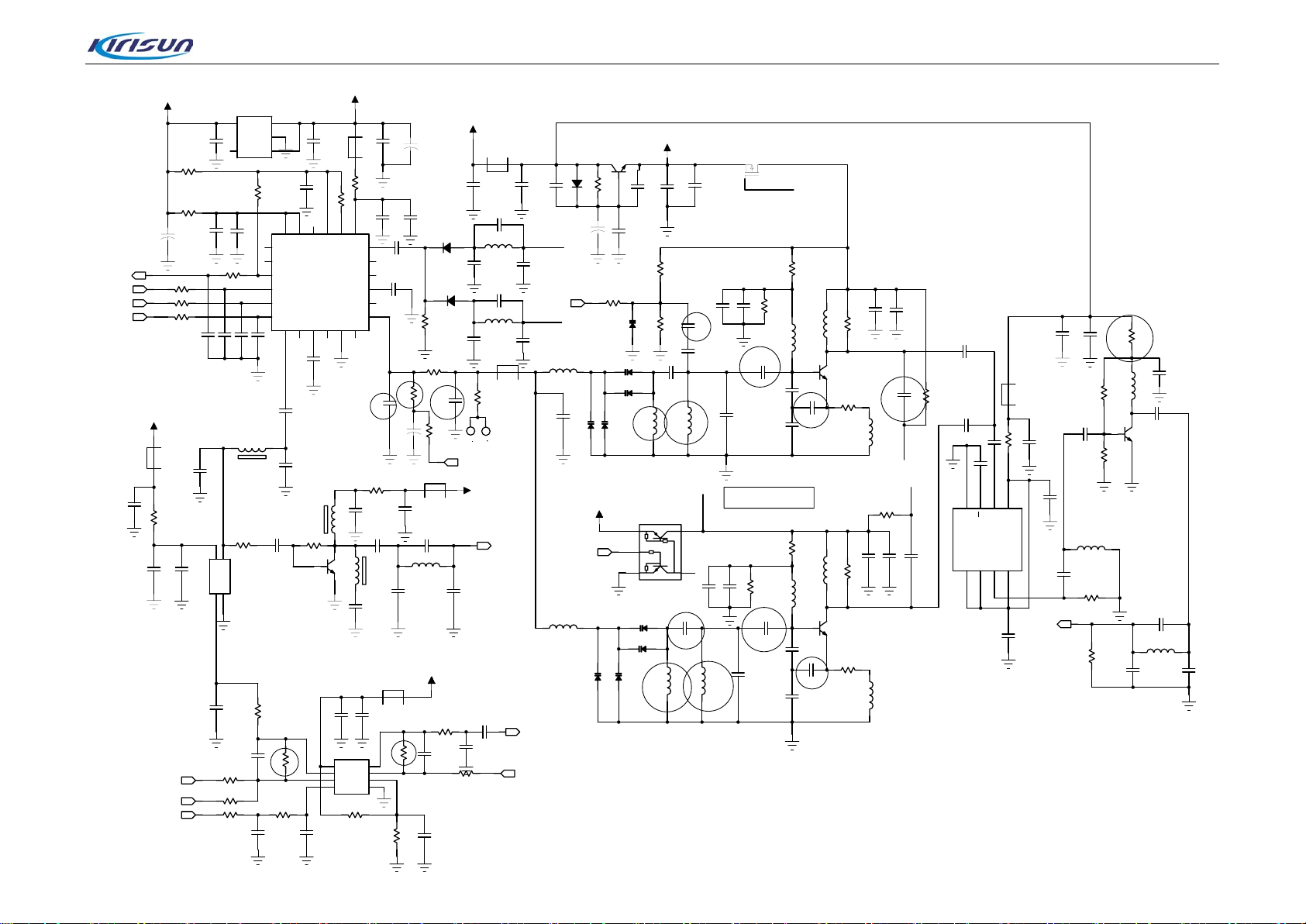
TP660 Service Manual
PLL_LD
PLL_DAT
PLL_CLK
PLL_CS
L631
BLM18AG601S
C691
103
PLL3V3
+
R642 100R
R643 100R
R629 100R
PLL3V3
R627
100R
C638
104
MOD_Q
CTC/DCS_OUT
MOD2_BIAS
560nH
R639
330K
5C
C667
C666
105
470P
L603
BLM18AG601S
R609
10R
10K
R632
C669
470P
5
19NC7
24
VDD
2
MUX
C-
FVCO
VC CP
15
NC
16
U601
L607
NC
3
/FVCO
14
NC
6
GND
XTALOUT8/OSC
18NC12
C649
102
C650
224
R640
470R
C644
103
L608
470nH
C645
180P
C683
C682
105
104
8
1
V+
AOUT
2
7
A-IN
BOUT
3
6
A+IN
B-IN
5
4
B+IN GND
U603
NJM2904V
R648
18K
C677
183
U602
XC6204B332MR
5
1
OUT
VIN
C665
104
R634
10R
R630
10R
C662
470P
C664
4.7U/10V
R628
C656
C657
C655
100P
100P
103
C636
10P
3
4
C639
VCC
102
X601
16.8MHz
GND OUT
1VC2
C640
332
100K
R641
560K
R605
15K
VSS
4
CE
NC
R631
10K
C663
104
23
13
1K
20
22
21
C658
100P
L601
3.3uH
R638
10K
R646
C678
100P
C686
2
3
C637
104
1
11
MOD
C-C
VC EL
VCC-XTAL
NC
4
PS
SKY72310
DATA
CLK
/CS CPOUT
OSC
9
17NC10
C634
470P
C635
10P
C643
47P
Q605
2SC5066(Y)
4K7
R644
220K
R615
22K
153
PLL&VCO Circuit
5C
C676
104
C693
470P
C659
100P
R635
EC651
2.2uF/10V
C695
103
C646
103
L610
BLM18AG601S
R651
180K
120R
C647
R649
9K1
+
+
330nH
33P
EC668
10uF/10V
MA2S077
R658
4K7
R636
56R
C652
224
R660
NC
L632
BLM18AG601S
C648
68P
L609
5C
R652
C681
100P
C680
105
D611
D612
MA2S077
10K
L630
BLM18AG601S
C654
103
R650 100KR645
C685
C670
105
470P
C689
3P
L602
15nH
F_RXVCO
C661
C660
6P
6P
C801
4P
L633
18nH
F_TXVCO
C803
C802
6P
6P
L600
BLM18AG601S
R637
10K
1
1
TP602
TP601
CV
CV
FL
5R
2ND_LO
C688
NC
C692
105
C687
332
C653
MOD_VCO
MOD_I
MOD_VCO
390nH
470P
390nH
MA2S111
L611
VCOVCC_SW
L619
D601
EC671
10uF/10V
D606
R623
4K7
HVC376B
D604
Q606
2SC4617(S)
C673
470P
+
C672
103
R620
4K7
D610
1SV278
D609
HVC350B
D608
HVC350B
D607
HVC376B
VCOVCC
34
2
1
D603
HVC350B
D602
HVC350B
D605
HVC376B
HVC376B
VCOVCC
C675
C674
103
105
R621
150K
R622
68K
L612
27nH
UMC4N
L620
27nH
C608
1P
C609
0P5
C601
10P
L613
27nH
U604
RXVCO_VCC
5
C620
8P
L621
15nH
C610
104
NC
C603
VCOVCC_SW:T:0V;R:3.3V
C628
C627
470P
104
Q607
2SJ243
C611
470P
C622
NC
C604
R612
C623
10P
RXVCO_VCC
R602
4K7
12P
4K7
R601
5K6
C612
C613
104
470P
R604
L616
100R
390nH
L615
390nH
C614
Q601
C605
18P
C606
15P
C624
18P
C625
10P
2SC3356
C617
R603
3P
C607
33P
C626
120R
L614
390nH
F_TXVCO
R608
4K7
F_RXVCO
R611
5K6
L623
390nH
L622
390nH
39P
R614
100R
Q603
2SC3356
C629
C630
104
470P
R613
120R
L624
390nH
1P5
R659
4K7
C631
1P5
4
GND
C804
1P5
UPB1509GV
SW16SW27OUT8VCC2
5
L629
BLM18AG601S
C632
6P
C805
3
U605
C806
R610
10R
102
102
C616
1
470P
IN2IN
VCC1
C807
C690
102
C615
C619
470P
10P
LO
R619
104
330R
C684
102
L625
82nH
R616
5K6
C618
15P
R617
3K9
L617
82nH
R606
1K
R680
1K
C700
10P
Q604
2SC5066(Y)
C633
12P
C699
7P
L626
39nH
C698
5P
Page 64 of 65
Page 68

Figure 6 TP660 Keyboard Schematic Diagram
SWB+
L106
EXT_SP-
EXT_SP+
CON14
CN102
H2
HOLE
1
H3
HOLE
+
BA
P2
SW-KEY
2
SW-KEY
6
SW-KEY
22
SW-KEY
1
C105
22uF/10V
R129
10R
C110
104
1
2
3
4
5
6
7
8
9
10
11
12
13
14
H4
HOLE
C160
104
C103
270P
C100
270P
BOOT_CTRL
RX_AUDIO
RSSI
USB_D+
USB_D-
MSW
EXT_PTT
EXT_MIC
SWB
EX_SPEX_SP+
1
C159
470P
SPK1
16R/1.5W
SPEAKER
R134
R135 22R
C127 270P
P3
SW-KEY
3
SW-KEY
7
SW-KEY
0
SW-KEY
C128 270P
150K
R105
10K
10K
R125
C185
NC
C108
270P
2
1
+
C109
270P
22R
USB_D+
USB_D-
BV08C
D113
D112 BV08C
D111 BV08C
P4
SW-KEY
4
SW-KEY
C104
104
R107
IC101
TDA8547TS
11
18
OUT-
VCC2
3
OUT+
13
OUT2-
8
10R
OUT+
MODE
SELECT
GND21GND12NC7NC9NC12NC19NC
10
C111 100P
BV08C
D114
100P
C119
BV08C
D115
NC
NC
C121 100P
C123
C122
BV08C
BV08C
BV08C
D117
D116
D118
100P
C150 100P
C152 100P
C154
C151 100P
C153 100P
VCC1
SVRR
20
IN1+
IN2+
C155 100P
R106
C190
220P
150K
17
IN1-
16
14
IN2-
15
5
4
6
+
C188
EC103
105
100P
100P
C125
C124
BV08C
BV08C
D120
D119
K1
K2
K3
K4
K5
K6
K7
K8
100P
100P
C156
C180
R132
C191
220P
C101
R101
10K
R102
10K
C192
C193
332
332
NC
C161
NC
100P
Q103
DTC144EE
SELECT
C175
NC
C126
EXT_SPEXT_SP+
BV08C
D121
CN103
CON10
10
9
8
7
6
5
4
3
2
1
11 12
8
SW-KEY
11
SW-KEY
C130
R119
R133
330R
104
LED3
LED
330R
LED6
LED
R131
330R
LED2
LED
R120
330R
LED1
LED
C147 220P
R130
330R
LED4
LED
C140 NC
C141 220P
C142 220P
R115 NC
R114 2.7K
R124
100R
R121
330R
C170
104
LED5
LED
H1
HOLE
P1
SW-KEY
1
SW-KEY
5
SW-KEY
9
SW-KEY
1
BLM21P300S
C102
105
105
C158
NC
R116 2.7K
C157
103
Q105
DTC144EE
R123 0R
C143 220P
R117 2.7K
C167
105
TP102
AF
R136
10K
MODE1
C144 220P
Q107
FMMT717
1
C162
103
EXT_MIC
R118 2.7K
F101
0.5AFUSE
Q104
DTC144EE
12
R138
47K
MODE2
C145
104
R137
2K2
DTC144EE
Q106
C163
NC
C132
470P
C146
470P
C131
105
VOL_OUT
R3
1K
C129
470P
LAMP
L102
BLM11A221S
TP660 Service Manual
MIC_5V
R109
470R
C133
EC120
103
4.7uF/10V
MK2
1
MIC
2
C148
470P
+
C181
105
4.7uF/10V
EC131
+
C118
L105
BLM11A221S
TP101
MIC
1
MIC_5V
C166
105
BLM11A221S
R110
104
1K
C117
470P
L101
Q102
2SJ243
L104
L103
BLM11A221S
R108
100K
USB_D+
USB_D-
3V3
L107
BLM11A221S
SWB+
Q101
DTC144EE
TP106
D+
1
BOOT_CTRL
BLM11A221S
VOL_OUT
LAMP
MSW
MODE1
MODE2
SELECT
TP105
1
D-
EXT_PTT
L_CS
L_LSK
L_SLD
L_RES
L_AO
K1
K2
K3
K4
RSSI
MIC_IN
SWB+
38
37
36
35
34
33
32
31
30
29
28
27
26
25
24
K5
23
K6
22
K7
21
K8
20
19
18
17
16
15
14
13
12
11
ME
10
9
8
7
6
5
4
3
2
1
40 39
CON38
CN101
Page 65 of 65
 Loading...