

Page 1

Page 2

PT8100 Service Manual
Dangerous!
Do not connect the AC power or DC power over 18V with
any connector or terminal of the radio. Otherwise it will cause
fire, electric shock or damage to the radio.
Warning!
Do not reverse power connection.
Do not turn on the radio before the antenna or load
connection is completed.
Do not touch the antenna while the radio is transmitting,
otherwise, it may cause light burning on skin.
The radio is not waterproof, so it's better to avoid putting it
in rain or snow, or any other liquid to ensure its life and
performance.
Statement!
Kirisun Electronics (Shenzhen) Co., Ltd owns the
copyright of KSP8100 software.
Unauthorized Duplication of KSP8100 software is strictly
prohibited.
Kirisun Electronics (Shenzhen) Co., Ltd owns the
copyright of the MCU software.
Kirisun Electronics (Shenzhen) Co., Ltd owns the
copyright of the radio outward appearance/structure/circuit
design.
Kirisun Electronics (Shenzhen) Co., Ltd owns the
copyright of this service manual. Unauthorized publication is
prohibited.
Kirisun Electronics (Shenzhen) Co., Ltd owns the
trademarks “KIRISUN”, “
立讯”.
”, “ ”, and “科
Contents
Chapter 1 Overview ...............................................................................1
Chapter 2 Unpacking and Checking....................................................... 1
Chapter 3 External View and Functional Keys....................................... 2
Chapter 4 Circuit Description................................................................. 4
Chapter 5 Mode Introduction .................................................................9
Chapter 6 Disassembly and Assembly for Maintenance.......................10
Chapter 7 Adjustment........................................................................... 12
Chapter 8 Specifications....................................................................... 16
Chapter 9 Troubleshooting ................................................................... 16
Appendix 1 Abbreviations.................................................................... 17
Appendix 2 Electronic Parts List.......................................................... 17
Appendix 3 Structural Parts List .......................................................... 22
Appendix 4 Accessories .......................................................................22
Figure 1 PT8100 Block Diagram..........................................................23
Figure 2 PT8100 Main Board Schematic Circuit Diagram...................24
Figure 3 PT8100 Main Board Top Layer Position Mark Diagram ....... 25
Figure 4 PT8100 Main Board Top Layer Position Value Diagram....... 26
Figure 5 PT8100 Main Board Bottom Layer Position Mark Diagram..27
Figure 6 PT8100 Main Board Bottom Layer Position Value Diagram .28
Figure 7 PT8100 Key Board Schematic Circuit Diagram .................... 29
Figure 8 PT8100 Key Board Top Layer Position Mark Diagram......... 30
Figure 9 PT8100 Key Board Top Layer Position Value Diagram......... 31
Figure 10 PT8100 Key Board Bottom Layer Position Mark Diagram .32
Figure 11 PT8100 Key Board Bottom Layer Position Value Diagram . 33
Page 3
PT8100 Service Manual
Chapter 1 Overview
1.1 Introduction
This manual applies to the service and maintenance of
PT8100 mobile radios, and is intended for use by engineers and
professional technicians that have been trained by Kirisun. It
contains all required service information for the equipment.
Kirisun reserves the right to modify the product structure and
specifications without notice in order to enhance product
performance and quality. You can also log on our website
www.kirisun.com
contact your local dealer or us.
Please read this manual before repairing the product.
1.2 Service Attentions
* Safety
Do not touch the antenna connector while repairing the radio.
Do not reverse the battery polarity.
Do not turn on the radio before the antenna or load
connection is completed.
Do not touch the antenna while the mobile radio is
transmitting, otherwise, it may cause light burning on skin.
* Explosive Atmosphere
It’s prohibited to use or repair the radio in the following
places:
Hospital, health center, airport
Any area with a potentially explosive atmosphere (e.g. orlop
deck of the ship, storage or transportation equipment for fuel and
chemical etc.)
Any place near blasting sites or area with electrical blasting
cap.
* Replacement Parts
All components used for repair should be supplied by
Kirisun.
Components of the same type available on the market are not
surely able to be used in this product and we do not guarantee the
quality of the product using such components.
If you want to apply for any component from Kirisun, please
fill in an application form as below.
e.g.
Component Application Form
Radio
Model
PT8100-01 FET Q18 3SK318 105-3SK318-R01 1
PT8100-01 Triode Q5 2SC3357 104-SC3357-R01 1
to download the latest service manual or
Component
Position
Mark
Model/
Specifications
Part No. Qty
1.3 Service
All the Kirisun products are subject to the service warranty.
After-sales service will be provided, and the length of
warranty is stated by Kirisun. The radio and its accessories are all
in the warranty. However, in one of the following cases, charge
free service will be not available.
* No valid warranty card or original invoice.
* Malfunction caused by disassembling, repairing or
reconstructing the radio by the users without permission.
* Wear and tear or any man-made damage such as mechanical
damage, burning or water leaking.
* Product’s serial number has been damaged or the product
trademark is difficult to identify.
After the warranty expires, lifetime service is still available.
We also provide service components to service stations and staffs.
Chapter 2 Unpacking and Checking
2.1 Unpacking and Checking
Unpack the radio carefully. We recommend that you check
the radio and the supplied accessories listed in the following table
before discarding the packing material. If any damage or loss has
occurred during shipment, please contact the dealer without
delay.
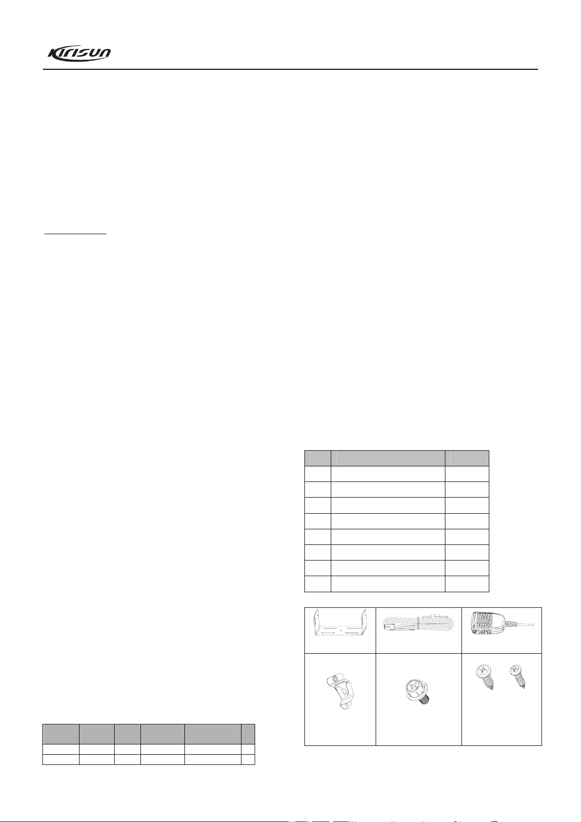
No. Item Qty
1 Mounting Bracket 1
2 Power Cable 1
3 Hand Microphone 1
4 Microphone Hanger 1
5 M4*10 SEMS Screw 4
6 M4*16 Self-tapping Screw 2
7 M5*16 Self-tapping Screw 4
8 Instruction Manual 1
Mounting Bracket
Microphone Hanger
1
Power Cable Hand Microphone
M4*10 SEMS Screw
M5*16 / M4*16
Self-tapping Screw
Page 4
PT8100 Service Manual
2.2 Licenses
It is requested by rules that each radio installation site (for
mobile station or base station) should be provided with a license.
The license carrier should guarantee that the Tx power, frequency
and deviation comply with the license requirements.
Transmission adjustment can only be conducted by
license-authorized technicians. Installation or operation of the
radio does not need a license.
2.3 Check before Installation
Every radio has been adjusted and checked before shipment.
Before installation, it’s better to check if the radio’s
transmission and receiving are normal to make sure its proper
operation.
The test should be performed with all cables and accessories
correctly connected.
Tx frequency, deviation, and power output should be checked,
as should Rx sensitivity, squelch, audio output, and signaling
operation.
2.4 Installation
1) Preparation
Check the vehicle and decide how and where to install the
radio antenna and accessories. Make sure that the cable will not
be extruded. And pay attention to the heat dissipation of the radio
to avoid overheating.
2) Antenna
The best position for the antenna is in the center of an open
and flat conduction region, usually the center of the vehicle roof
or the cover of the luggage trunk. Connect one end of the earth
wire to the cover of the luggage trunk and the other end to the car
outer shell so that the cover of the luggage trunk is grounded.
3) Connection of Power Cable
* First of all, please check whether there is a hole for the power
cable on the insulating board. If no, please bore the board with a
suitable drill bit and fix a rubber grommet on it to protect the
cable from abrasion.
* Afterwards, please pass the cable through the insulating board
and lead from the car into the engine room. Connect the red
conductor to the positive terminal of the accumulator and the
black conductor to the negative terminal.
* At last, ring the remained conductor and fix it.
Note: Please guarantee sufficient relaxation of the power
cable in the car so that the radio can be conveniently
disassembled, assembled, and repaired in the state of power
connection.
4) Installation
Warning: For passenger safety, please install the radio
securely using the supplied mounting bracket so that the
radio will not be loosened in case of collision.
* Take the mounting bracket as the sample to draw the position of
the four holes for screws. Then drill the holes on the instrument
panel, and then install the mounting bracket with 4 M5*16
self-tapping screws. (Note: Please install the radio at a position
convenient for operation, and leave enough space for connection
of the cable.)
* Slide the radio into the mounting bracket and fix it to the
bracket with 4 M4*10 SEMS screws (with flat washer and spring
washer). (Set an appropriate height and angle for the radio by
using different screw holes of the bracket.)
* Connect the antenna and the power cable to the radio.
* Install the microphone hanger at an appropriate position using 2
M4*16 self-tapping screws. (It should be made sure that the
microphone and its cable will not affect safe driving.)
* Connect the microphone to the MIC jack on the front panel of
the radio and put the microphone on the hanger.
Note: When replacing the fuse of the power cable, only use
fuses of the same type and rating; otherwise the radio could
be damaged.
5) Attention
If you have no plan to use external speaker, please cover the
speaker jack with the supplied rubber plug to prevent dust and
sand getting in.
Chapter 3 External View and Functional Keys
3.1 Front Panel
4
5
7
6
① Power Button
Press and hold this button (1.5 seconds or longer) to turn the
radio power ON or OFF.
② LED Indicator
Lights red while the radio is transmitting, lights green while
the radio is receiving.
Flashes orange while receiving DTMF, 2Tone or 5Tone
signals the same as the setting of the radio.
Flashes red while the radio is scanning (This function can be
2
2
3
8
1
9
Page 5
PT8100 Service Manual
enabled/disabled by PC software).
③ LCD Display
Refer to “LCD Display Screen” for details.
④ Volume Knob
Adjust volume of the mobile radio.
⑤ MIC Jack/Programming Interface
⑥ P1 Button (Programmable Button)
⑦ P2 Button (Programmable Button)
⑧ P3 Button (Programmable Button)
⑨
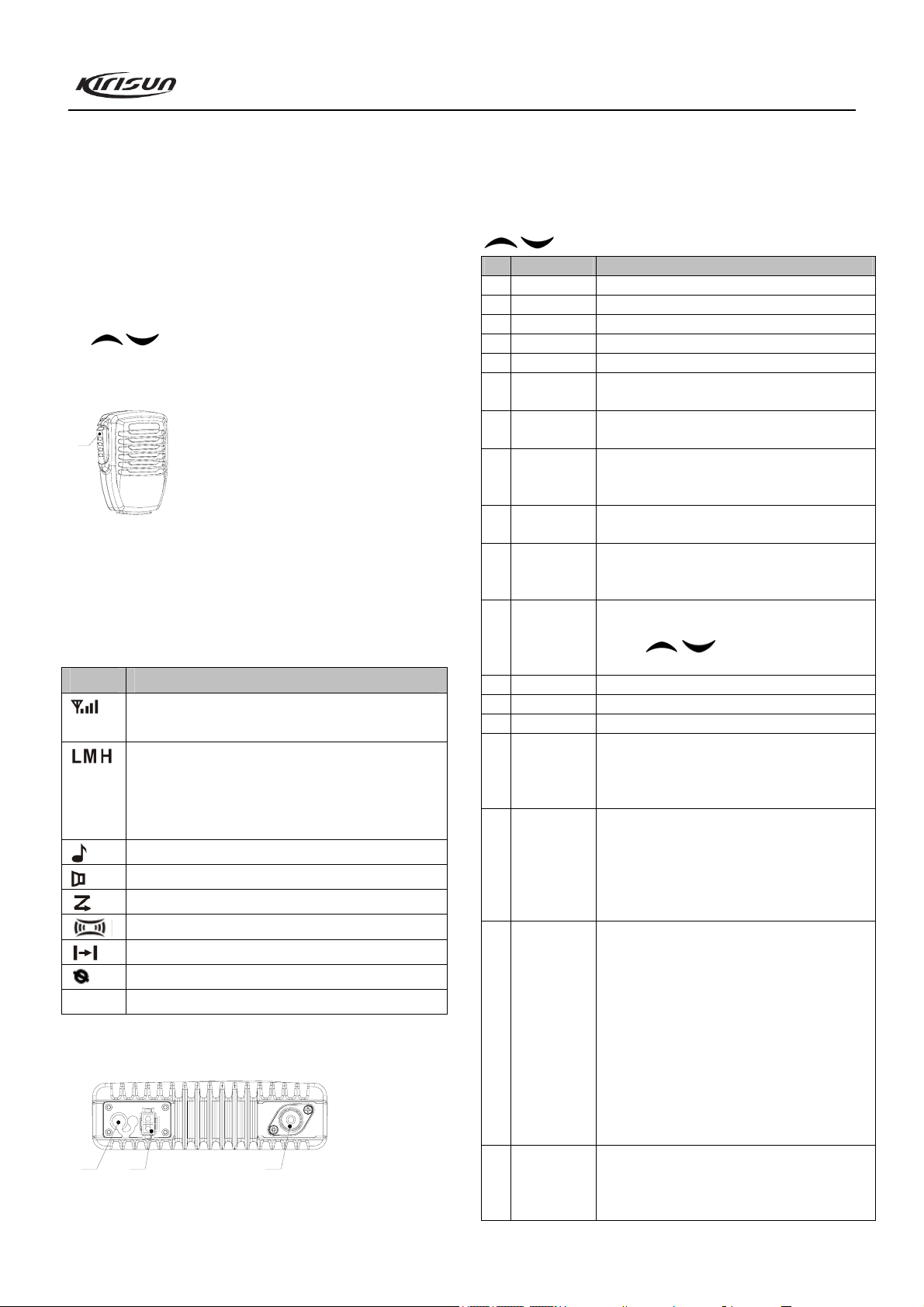
3.2 Microphone
⑩ PTT Button (on the hand microphone)
microphone, your voice can be transmitted to the recipient.
Release PTT to receive.
3.3 LCD Display Screen
Display Description
P2 Appears when the radio is in OST state.
3.4 Rear Panel
① Antenna Connector
/ Button (Programmable Button)
⑩
Press and hold the PTT button, then speak into the
Shows the strength of the received signals; 4 bars
indicates the strongest signal.
Shows the transmitting power level of the radio:
‘L’ indicates low Tx power level;
‘M’ indicates middle Tx power level;
‘H’ indicates high Tx power level.
Appears when the radio receives a Sel Call/Call Alert.
Appears when the radio is in “Monitor” state.
Appears when the radio is scanning.
Function not used.
Appears when the radio is in talk-around mode.
Function not used.
①②③
② Power Terminal
③ External Speaker Jack
3.5 Auxiliary Functions for Programmable Buttons
The following auxiliary functions can be assigned to
/ ,P1,P2,P3 buttons by the distributor.
No. Function Description
0 None No function is assigned.
1 Channel Up Select the next channel.
2 Channel Down Select the previous channel.
3 Zone Up Select the next zone.
4 Zone Down Select the previous zone.
5 Display CH
Frequency
6 Display CH
Alias
7 Display Mode
Switch
8 OST This allows the radio user to change the QT/DQT setting
9 Power Level This allows the radio user to adjust the transmit power
10 Squelch Level Press the button to enter “Squelch Level Adjustment
11 Key Lock Press to lock/unlock some keys.
12 Scan Press to start/stop scanning.
13 FCS Press to start free channel scanning (FCS).
14 Nuisance Delete
(temporarily)
15 Public Address Press to enable the public address function. When press
16 Home Channel Press the button to switch to the preset home channel. If
17 Talk Around Press the button to toggle between Repeater Mode and
Press the button, frequency of the current channel will be
shown on the LCD.
Press the button, alias of the current channel will be
shown on the LCD.
Press the button to switch the display mode between
“Channel No.”, “Channel Alias”, “Zone No.”, “Zone
Alias”, and “Channel Frequency”.
of current channel by pre-programmed OST list.
setting to “High”, “Mid” or “Low”. Meanwhile, the LCD
will display “H”, “M”, “L” respectively.
Mode”, then the user can adjust the squelch level by
pressing / . Press P3 button to save the
selected squelch level and the radio then quits this mode.
When the radio lands on an unwanted channel during
scanning, press the button to delete this channel
temporarily. When exit scan mode and enter it again, the
channel will be added to the scan list again.
and hold the PTT key and speak to the microphone, your
voice will be heard by yourself and surround people
through the external speaker, but will not be transmitted.
Press this button again to disable the public address
function, and the radio returns to user mode.
the radio has set two home channels, it will switch to
home channel 1 upon pressing this button, and will switch
to home channel 2 if you press this button again within 2
seconds, and will switch to the original channel if you
press this button for the third time within 2 seconds.
When switching to the home channel, the zone is also
switched. If the radio has only set one home channel, the
radio will switch between the working channel and the
home channel upon pressing this button within 2 seconds.
If the interval between two pressings is longer than 2
seconds, the radio will always switch to home channel 1.
Talkaround Mode. In Talkaround Mode, the Rx
parameters are used in place of the Tx parameters when
transmitting.
3
Page 6
PT8100 Service Manual
18 Momentary
Monitor / Call
Cancel
19 Monitor/Call
Cancel
20 Momentary
Squelch Off /
Call Cancel
21 Squelch
Off/Call Cancel
22 Emergency Press the button to make an alarm tone according to the
23 Call 1 Press to send the preset code.
24 Call 2 Press to send the preset code.
25 Call 3 Press to send the preset code.
26 Call 4 Press to send the preset code.
27 Menu
Select/Enter
28 Lone Worker Press to enable/disable Lone Worker function.
29 Scan List Edit This allows the radio-user to edit a Scan List. Scan List
30 Backlight Press to toggle between “Light”, “Dark” and “Auto” for
Chapter 4 Circuit Description
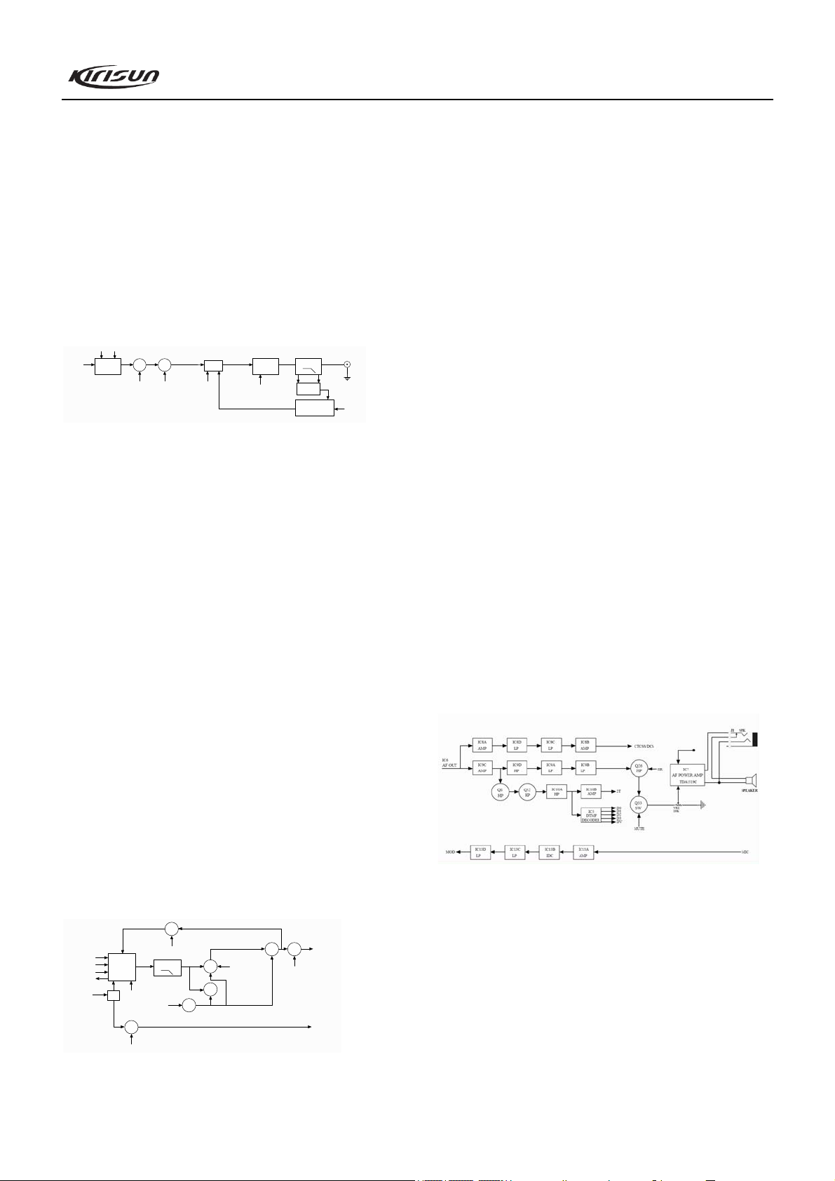
4.1 Frequency Configuration
ANT
ANT SW RF AMP
The receiver adopts double mixing. The first IF is 49.95MHz
and the second IF is 450kHz.
The first local oscillator signal of the receiver is generated by
the frequency synthesizer and the second local oscillator signal is
generated by frequency tripler X1.
The transmitter signal is produced by the frequency
synthesizer.
The reference frequency of the frequency synthesizer is
Press and hold the button, QT/DQT/2Tone/5Tone/DTMF
signaling will be closed. Release the button to return to
normal operation. Press the button during the Select Call
state, the radio will exit Select Call state.
Press the button to close QT/DQT/2Tone/5Tone/DTMF
signaling, then you can receive signals that cannot be
received during normal operation. Press the button again
to resume normal operation. Press the button during the
Select Call state, the radio will exit Select Call state.
Press and hold the button to open squelch; release it to
resume normal operation.
Press it during the Select Call state, the radio will exit
Select Call state.
Press the button to open squelch; press it again to resume
normal operation.
setting of the programming software or send your ID or
background sound to your partner or the system.
Press to enter the Menu Mode, to make menu selections
and save.
editing is only available for Scan Lists where the User
Programmable field has been enabled.
the backlight.
CF2
450KHz F
CF1
450KHz H
MCF
49.95MHz
RX
TX
16.8MHz
IF SYSTEM
TCXO
X3 multiply
AF AMP
MIC AMPPLL VCOTX AMPPA AMP
Figure 4.1 Frequency Configuration
provided by TCXO.
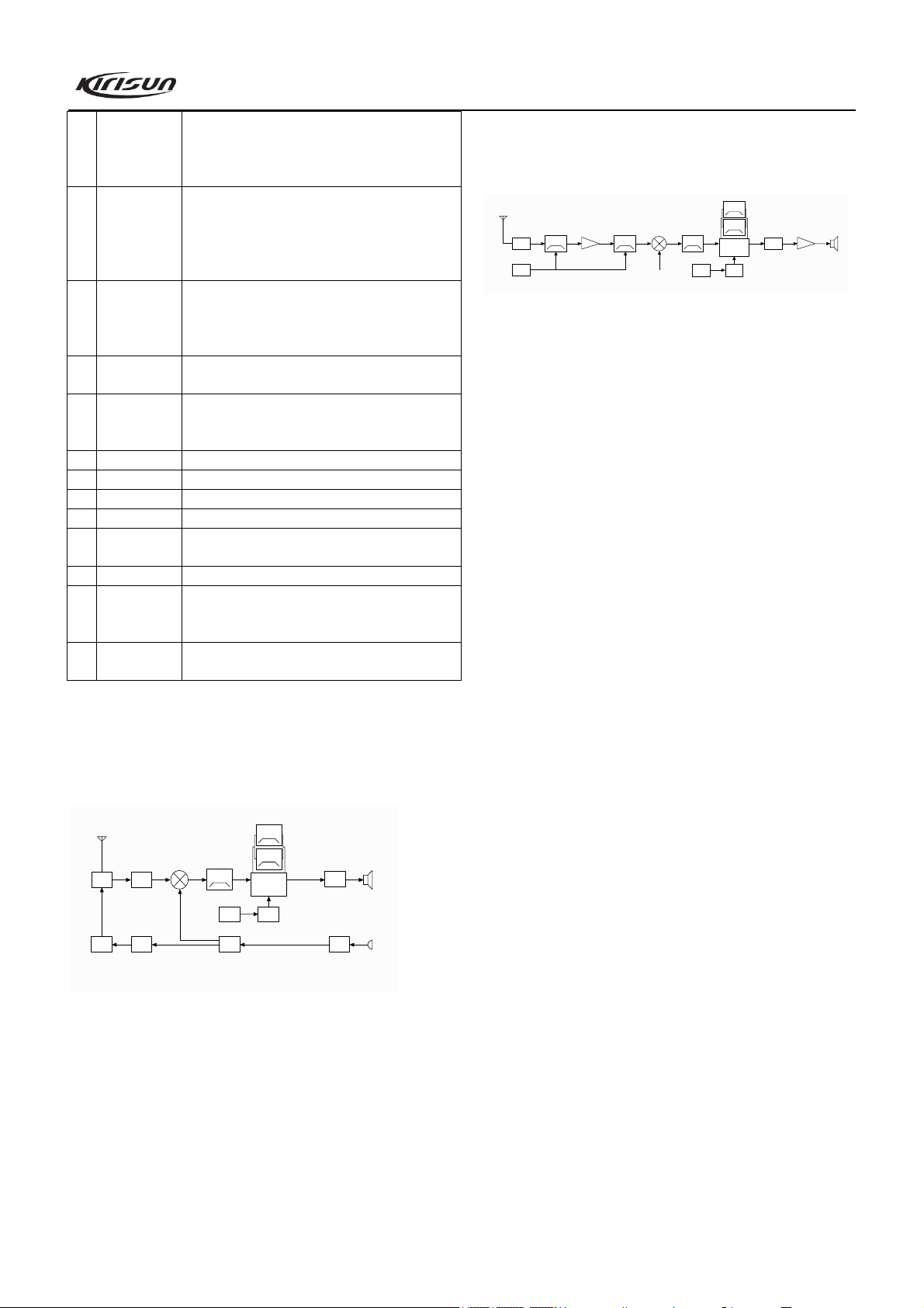
4.2 Principle of Receiver (RX)
CF2
49.95MHz
450KHz F
CF1
450KHz H
MCF
IF SYSTEM
IC4
TCXO
X3 multiply
16.8MHz
NJM2902
IC9 TDA1519C
IC9
AF AMP
ANT
D3 D11
ANT SW
IC11
MCU
Q18
BPF
RF AMP
Q19
BPF
1st Local OSC
Figure 4.2 Principle of Receiver
Front end
The signal coming from the antenna passes through the
RX/TX switch circuit (D3 and D37), and passes through a BPF
consists of two LCs to remove unwanted out-of-band signals, and
then is routed to the low noise amplifier (LNA) consists of Q18
and its peripheral components where it is amplified.
Output signal from the LNA passes through a BPF consists of
three LCs to further remove unwanted out-of-band signal, and
then goes to the first mixer (Q19).
AGC circuit
AGC circuit, which consists of Q16 and its peripheral circuit,
will work to reduce the gain of Q18 only when the input signal is
too large.
First mixer
The Rx signal from LNA is mixed with the first local
oscillator signal from the frequency synthesizer to produce the
first IF signal (49.95MHz).
IF circuit
The first IF signal passes through the crystal filter (XF1) to
remove the adjacent channel signal and signal outside the
adjacent channel. Then the filtered signal is amplified by the first
IF amplifier (Q20), and is sent to the IF processing IC (IC6,
TA31136).
IF IC consists of the second mixer, IF amplifier, limiter,
discriminator, noise amplifier, and audio low pass filter.
Signal (16.8MHz) from X1 is multiple-amplified by Q11 and
its peripheral circuit to produce the second local oscillator signal.
Then the second local oscillator signal (50.4MHz) is mixed with
the first IF signal (49.95MHz) in IC6 to generate the second IF
signal (450kHz). And then the second IF signal is amplified and
limited in IC6, filtered by its ceramic filter (CF1 or CF2,
450kHz), and then demodulated in IC6. After that, the
demodulated signal is routed to the audio circuit to output audio
signal.
The selection circuit of the second IF filter consists of CF1,
CF2, D20, D21, and the peripheral circuit. When the mobile radio
is set to wideband, CF2 is put through and takes effect, while
4
Page 7
PT8100 Service Manual
CF1 is cut off; when the mobile radio is set to narrowband, CF1
is put through and takes effect, while CF2 is cut off.
Squelch circuit
The demodulated signal from IC6 is sent to the internal noise
amplifier in IC6. Then the resulting signal is further amplified in
Q21 and demodulated in D25, and then the resulting DC level is
sent to the MCU squelch control circuit. This voltage is in inverse
proportion to the input signal.
4.3 Principle of Transmitter (TX)
TX power amplification
8T 8R
VCO
TX/RX SW
Q5
Q4
PRE
RF AMP
DRIVE
8T
8T
Figure 4.3 Principle of Power Amplifier and Antenna Switch
The modulated RF signal from VCO is amplified by Q1, Q2,
Q4, and Q5, and is sent to IC1 for power amplification. Output
power of IC1: 25W.
Grid bias of IC1 is controlled by the APC circuit. Through
changing the grid bias voltage, the Tx output power can be
controlled conveniently.
APC(Automatic Power Control)circuit
D9 and D10 are RF detector diodes. The output power of the
RF amplifier is detected by RF detector diodes and converted into
DC level. Then the DC level is compared with the signal from
MCU and amplified in IC4, and is sent to grid in IC1 to control
the power output.
If the Tx output power is too high, the voltage detected by the
detector diodes will increase; IC4 output voltage will decrease, so
the bias voltage imposed on IC1 will also decrease, which causes
the Tx output power to be lowered, and vice versa. Thus, the Tx
output power can keep stable under different working conditions.
MCU can set the power through changing the voltage input to
IC4.
4.4 Principle of Frequency Synthesizer
BUFF
UL
IC3
CK
QT TCXO
PLL IC
MB15E03SL
DT
UL
X1
TCXO
16.8MHz
3.5V
*3 2ND LOCAL AMP
Q11
8R
LOOP FILTER
5V
Figure 4.4 Frequency Synthesizer
PT8100 adopts PLL type frequency synthesizer.
IC1
RA30H
13.8V
Q7
5V
Q6
TX
VCO
Q14
RX
VCO
Q14
RIPPLE
FILTER
ANT SW
8T
Q1 Q2
RF AMP
BUFF
MOD
5V
2ND LOCAL
LPF
IC4
APC CONTROL
TO ANT
APC
VCO OUT
The frequency synthesizer consists of reference oscillator,
voltage control oscillator (VCO), programmable divider, phase
comparator, and low pass filter (LPF).
Tx VCO unit consists of Q6, D1, D4, D5, and D6. D8 is the
modulation circuit of Tx VCO.
Rx VCO unit consists of Q12, D14, D16, D17 and D18.
IC3 (MB15E03SL) is the PLL integrated circuit, which
consists of programmable reference divider, programmable
divider, phase comparator, and charge pump.
The low pass filter consists of R54 and C113.
The reference frequency is provided by X1 (TCXO,
16.8MHz).
Reference frequency from TCXO (Temperature-Controlled
Crystal Oscillator) is divided by the programmable reference
divider in IC3 to produce reference frequency of 5kHz or
6.25kHz (determined by the preset channel frequency and is
controlled by MCU).
The oscillation frequency from VCO goes to IC3 where it is
divided by the programmable divider and is then compared with
the reference frequency to obtain the error signal. The signal is
then filtered by a low pass filter and is sent to VCO to change the
oscillation frequency of the VCO, enabling the frequency to
reach the set value. Then the VCO is locked.
Unlock detection: When PLL is unlocked, pin14 of IC3 will
output low level signal to MCU. Then MCU prohibits the Tx
from transmitting and makes an alert tone.
4.5 Audio Processing Circuit
Figure 4.5 Audio Processing
MIC signal processing:
Voice signal from MIC is sent to IC13A for amplification
(IC13A, D32, Q32 and other components form the AGC circuit to
improve the dynamic range of the circuit). Then the resulting
signal is pre-emphasized by C322 and R267 and goes to the IDC
circuit consists of IC13B. After being limited, the signal is
switched into wideband or narrowband in Q30 and then passes
through the low pass circuit consists of IC13C and IC13D to
remove signals above 3000Hz. Then the filtered signal is sent to
VR2 to adjust the deviation and modulated by D8, and then is
5
Page 8

PT8100 Service Manual
sent to Tx VCO.
Rx audio signal processing:
Voice signal from IC6 is divided into two parts. One branch
of the signal is routed to the low pass circuit consists of IC8,
where it is amplified and filtered (to remove the voice signal) to
obtain more purified CTCSS/DCS signal, which is then sent to
MCU for processing. The other branch of the signal goes to IC9.
After being amplified by IC9C (Q29 is the gain switching circuit
which is used to switch volume between wideband and
narrowband), the signal is divided into two branches again. One
branch is sent to the 2-tone (5-tone) shaping circuit consists of
Q8, Q52 and IC10, where it is shaped into better square wave
signal, and then is sent to MCU to judge the 2-tone (5-tone)
signal; the other branch passes through the high pass circuit
consists of IC9D to remove the sub-audio signal and passes
through the de-emphasis circuit consists of R173 and C245. Then
the de-emphasized signal is passed through the low pass circuit
consists of IC9A and IC9B and the high pass circuit consists of
Q26. After that, the resulting signal goes to the volume switch
where the signal volume will be adjusted. After being amplified
in IC7, the signal will be output to drive the speaker.
Impedance of the speaker: 16
Note:
* None of the terminals of the speaker should be grounded.
* The emergency alarm sound has no volume limit.
4.6 Power Supply:
The radio uses 13.8V battery, and the Tx power amplification
circuit (IC1) and Rx audio power amplifier (IC7) directly adopt
the battery for power supply.
IC17: 3V, LDO, micropower regulator, which supplies power for
MCU, DTMF decoding unit etc.
IC16: 8V, LDO, micropower regulator.
Q38: 8T switch, which is controlled by MCU.
8T: Supplies power for front end of transmitter.
Q40: 8R switch, which is controlled by MCU.
8R: Supplies power for RF amplifier and mixer of the receiver.
4.7 MCU Unit
MCU unit controls the operation of each unit of the radio so
that all functions can be realized.
Communicate with external PC.
Access the status data of the radio.
Control the PLL to generate Rx and Tx local oscillator
frequencies.
Obtain status parameters of the working channel.
Control status of LED indicator.
Control power supply for each unit.
Check the actions of each functional key.
Generate CTCSS signal.
Generate DCS signal.
Generate power control signal.
Perform CTCSS decoding.
Perform DCS decoding.
Perform 2Tone (5Tone) decoding.
Test and control the squelch.
Control content of voice alert.
4.8 Memory (E
2
PROM, A T24C512)
The memory is stored with channel data, CTCSS/DCS data,
other data for function setting, and parameter adjusting data.
CTCSS/DCS signal encoding and decoding:
CTCSS/DCS signal (output from pin97, PWM wave)
generated by MCU is sent to TCXO for modulation; and the
CTCSS/DCS signal (output from pin98, PWM wave) is sent to
VCO modulation.
CTCSS/DCS signal from the receiver is sent to MCU for
decoding. MCU checks if the CTCSS/DCS signal in the receiving
signal matches the preset value of the radio, and determines
whether to open the speaker or not.
CTCSS
CTCSS (Continuous Tone Control Squelch System) is a
squelch control system which is modulated on carrier and is
guided by a continuous sub-audio signal. If CTCSS is set, the
communication between the transmitting and receiving radios can
be realized only when the two radios have set the same CTCSS
frequency. In doing this, disturbance from other signals can be
avoided.
PT8100 has 39 groups of standard CTCSS frequencies for
your selection. See Table 4.1.
CTCSS signal (PWM wave) is generated by MCU, and is
passed through low pass filter consists of RC to remove the high
frequency components (above 300Hz). Then the resulting signal
is routed to VCO for modulation.
Table 4.1 CTCSS Frequencies
No. Frequency
1 67.0 11 94.8 21 131.8 31 186.2
2 69.3 12 97.4 22 136.5 32 192.8
3 71.9 13 100.0 23 141.3 33 203.5
[Hz]
No. Frequency
[Hz]
No. Frequency
[Hz]
No. Frequency
6
[Hz]
Page 9
PT8100 Service Manual
4 74.4 14 103.5 24 146.2 34 210.7
5 77.0 15 107.2 25 151.4 35 218.1
6 79.7 16 110.9 26 156.7 36 225.7
7 82.5 17 114.8 27 162.2 37 233.6
8 85.4 18 118.8 28 167.9 38 241.8
9 88.5 19 123.0 29 173.8 39 250.3
10 91.5 20 127.3 30 179.9
DCS
DCS (Digital Code Squelch), which is used to control squelch,
is a series of continuous digital codes modulated on carrier
together with voice signal. If DCS is set, the speaker can be
opened only when the radio receives signal with the same DCS to
avoid disturbance of unwanted signals.
PT8100 has 83 standard codes (inverted and non-inverted) for
your selection. See Table 4.2.
DCS signal (PWM wave) is produced by MCU. It passes
through the low pass filter consists of RC to remove the high
frequency components (above 300Hz). Then the resulting signal
is sent to VCO and TCXO for modulation, with HF components
of the DCS signal being modulated by VCO, and the LF
components of the DCS signal being modulated by TCXO.
The DCS signal coming from the receiver is routed to MCU
for decoding. MCU checks if the DCS code in the received signal
matches the preset DCS of the radio, and determines whether to
open the speaker or not.
Table 4.2 DCS Codes
023 114 174 315 445 631
025 115 205 331 464 632
026 116 223 343 465 654
031 125 226 346 466 662
032 131 243 351 503 664
043 132 244 364 506 703
047 134 245 365 516 712
051 143 251 371 532 723
054 152 261 411 546 731
065 155 263 412 565 732
071 156 265 413 606 734
072 162 271 423 612 743
073 165 306 431 624 754
074 172 311 432 627
4.9 Semiconductor Data
MCU Description
Table 4.3 Port Description of MCU (MB90F882)
No. Port name
1 GLED P40 O Rx Green Indicator H: on
2NC
3 NC - -
4 NC - -
5 P5 P32 I P5 Button Input
6 P1 P33 I P1 Button Input
7 P2 P34 I P2 Button Input
8 P3 P35 I P3 Button Input
9 P4 P36 I P4 Button Input
10 POWER P37 I Power Button Input
11 N C
12 NC
11 NC - -
12 NC - -
13 VCC VCC - CPU Power Input
14 VSS VSS - GND
15 C C -
16 LCD RST P42 O LCD Reset Control
17 LCD BLC P43 O LCD Backlight Control
18 LCD DAT P44 I/O LCD Serial Data Input/Output
19 LCD WR P45 O LCD Write Clock Output
20 LCD RD P46 O LCD Read Clock Output
21 LCD CS P47 O LCD Chip Selection Signal Output
22 MICDAT P90 I
23 HOOK P91 I Hook Signal Input
24 DEV2 P92 O Max. Deviation Compensation
25 DEV1 P93 O
26 UL P94 I
27 CK P95 O PLL Clock Output
28 LE P96 O PLL IC Enable Pin
29 DT P97 O PLL Data Output
30 AVCC AVCC - Connect with VCC
31 AVRH AVRH - Connect with VCC
32 NC - -
33 AVSS AVSS - Connect with VSS
34 QT/DQT IN AN0 I(A/D0) QT/DQT Signal Input
35 RSSI AN1 I(A/D1) Signal Strength Input
36 BUSY AN2 I(A/D2) Busy Signal Input
37 TEMP AN3 I(A/D3) Power Amplifier Temperature Protection Input
38 NC - -
39 NC - -
40 NC - -
41 NC - -
42 VSS VSS - GND
43 DTMFD0 P71 I DTMF Detect Input
44 DTMFD1 P72 I DTMF Detect Input
45 DTMFD2 P73 I DTMF Detect Input
46 DTMFD3 P74 I DTMF Detect Input
47 RX P76 O
48 DTMFDV P75 I DTMF Decoding Valid Input
49 MD2 MD2 - Programming Test Point
50 MD1 MD1 - Programming Test Point
51 MD0 MD0 - Programming Test Point
52 RESET RST I Programming Test Point
53 SCL UI6 O E2PROM Clock Line
54 SDA UO6 I/O
55 TEST P82 O L:Writable
56 NC
57 RXD P84 I RS-232 Input, Programming Test Point
58 TXD P85 O RS-232 Output, Programming Test Point
59 NC - -
60 NC - -
61 NC - -
Pin
Name
I/O Function
Reserved: Hand MIC Digital Keypad Data
Input
PLL Unlock Detect Pin
H:Locked,L:Unlocked
TX/RX VCO Selection
H: TX, L: RX
7
Page 10
PT8100 Service Manual
62 INT IRQ20 I Power Detect Input
63 DVCC DVCC -
64 DVSS DVSS -
65 8TC PA2 O Tx Power Control H:On
66 8RC PA3 O Rx Power Control H:On
67 SBC P50 O Main Power Switch Control H: on
68 TXGSW P51 O Tx Gate Control L: Tx
69 PA P52 O Public Address Control H: PA
70 AF_MUTE P53 O Mute Control L: AF Mute
71 NC - -
72 NC - -
73 DTMF PPG6 O(PWM) DTMF/2T/5T/Beep Output
74 VCCN PPG7 O(PWM) Frequency Voltage Regulation Output VCCN
75 P00 P00 High Level Programming Test Point
76 P01 P01 Low Level Programming Test Point
77 MIC_MUTE P02 O Mute Control H: MIC Mute
78 AFCO P03 O
79 NC - -
80 NC - -
81 NC - -
82 PTT P07 I PTT Button Input
83 IGN P10 I Reserved: Ignition Switch Detect Input
84 EXT-ALARM P11 I Reserved: External Alarm Input
85 MAXAF P12 O
86 NC - -
87 NC - -
88 VCC VCC - CPU Power Input
89 VSS VSS - GND
90 X1 X1 - Oscillator
91 X0 X0 - Oscillator
92 SHIFT P15 O
93 W/N P16 O
94 W/N P17 O
95 APC PPG0 O(PWM) TX: Automatic Power Control Output
96 TV PPG1 O(PWM) RX:BPF Tuning Output
97 DCSTCXO PPG2 O(PWM) CTCSS/DCS Output to TCXO
98 DCSVCO PPG3 O(PWM) CTCSS/DCS Output to VCO
99 TONEIN TIO1 I 2T/5T Signal Input
100 RLED P25 O Tx Red Indicator H:Light
Table 4.4 Function Description of Semiconductor Components
Position
Mark
IC5 HT9172 DTMF decoder chip
IC14 PST9140NR MCU reset circuit
IC13 NJM2902V MIC amplification, limitation, filtering
IC3 MB15E03SL Frequency synthesizer
IC4 NJM2904 APC, Voltage comparison, driving
IC6 TA31136
IC9 NJM2902 Rx demodulated signal amplification and filtering
IC8 NJM2902 Rx CTCSS/DCS signal amplification and filtering
IC11 MB90F882 MCU
IC12 AT24C512
IC7 TDA7297D Rx AF power amplification
IC1 RA30H1317M Tx final power amplification
Model Function Description
Rx 2
limitation, demodulation, and noise amplification
E2PROM, memorizes channel frequency data,
function setting parameters, and adjusting status
parameters
AF Power Amplifier Control
L: Power Amplifier On
Max. Alarm Volume Control Switch
H: Controlled by Volume Switch
L: Max Volume at Emergency Alarm
Clock Beat Shift
H:On
Wideband/Narrowband Control
H:Narrowband L:Wideband (Reserved)
Wideband/Narrowband Control
H:Wideband L:Narrowband
nd
local oscillation, 2nd IF amplification,
IC17 TA78033AF 3V voltage regulation output
IC16 L7808CV 8V voltage regulation output
IC18 NJM78L05UA 5V voltage regulation output
IC19 UPB1509GV Frequency divider
Q9 DTC144EE APC control switch
Q12 2SK508NV Rx VCO oscillation circuit
Q14 2SC4617 VCO power filter
Q11 2SC5108 Rx 2
nd
local oscillation frequency multiplier circuit
Q16 2SK1829 Rx high power amplifier gain control switch
Q18 3SK318 Rx high power amplifier
Q19 3SK318 First mixer
Q1 2SC5108 VCO buffer amplifier
Q20 2SC5108 1st IF amplifier
Q21 2SC4617 Rx noise amplifier
Q22 DTC144EE Wideband/narrowband noise toggle switch
Q23 DTA144EE
Rx wideband/narrowband frequency discrimination
toggle switch
Q29 DTA144EE Rx wideband/narrowband toggle switch
Q30 2SK1824 Tx wideband/narrowband toggle switch
Q27 DTC144EE Beat shift control switch
Q33 2SK1824 Rx AF mute switch
Q45 2SK1824 Rx AF output switch, disconnect on emergency
Q28 DTC144EE AF power amplification control switch
Q35 DTA144EE Power switch of MIC amplification unit
Q40 KTA1298 8R switch
Q1 2SC5108 VCO buffer amplifier
Q38 KTA1298 8T switch
Q32 2SC4919 MIC AGC control switch
Q4 2SC3357 Tx 1st amplifier
Q5 2SC3357 Tx 2nd amplifier
Q46 2SK1824 Rx AF output switch, put through on emergency
Q6 2SK508NV Tx VCO oscillation circuit
Q3 2SC4116 Tx VCO control switch
Q7 2SC5108 VCO buffer amplifier
Q13 2SC4116 Rx VCO control switch
Q53 2SK1824 Speaker/PA toggle switch
Q54 2SK1824 Speaker/PA toggle switch
Table 4.5 Function Description of Diodes
Position Mark Model Function Description
D3, D37 L709CE Transmitter antenna switch diode
D12 MA2S111 Unlock detect diode
D14, D16, D17,
HVC376 Rx VCO oscillation varactor diode
D18
D7 HZU5ALL APC output voltage limiting diode
D2, D19 HSC277 VCO output switch
D20, D21 DAN222 Rx 2nd IF filter wideband/narrowband toggle
switch
D23 HVC355B Rx BPF varactor diode
D25 MA742 Noise demodulation
D27, D28, D30,
HVC376B Rx BPF varactor diode
D29
D32 1SS372 MIC AGC detect diode
D1, D4, D5, D6 HVC376 Tx VCO oscillation varactor diode
D8 1SV278 Tx VCO modulation diode
Table 4.6:Features of Crystal Filter XF1
Item Rated Value
Nominal center frequency 49.95MHz
Passband width ±7.5kHz or higher
8
Page 11
PT8100 Service Manual
40dB stop bandwidth ±20.0kHz or lower
Pulse 1.0dB or lower
Insertion loss 3.0dB or lower
Guarantee attenuation 80dB or higher
Terminal impedance 330
Table 4.7 Features of CF1 LTWC450H
Item Rated Value
Nominal center frequency 450kHz
6dB band width ±3.0kHz or higher
50dB band width ±9.5kHz or lower
Pulse 2.0dB or lower
Insertion loss 6.0dB or lower
Guarantee attenuation 47.0dB or higher
Terminal impedance 1.5k
Table 4.8 Features of CF1 LTWC450F
Item Rated Value
Nominal center frequency 450kHz
6dB band width ±6.0kHz or higher
50dB band width ±12.5kHz or lower
Pulse 2.0dB or lower
Insertion loss 6.0dB or lower
Guarantee attenuation 47.0dB or higher
Terminal impedance 1.5k
Chapter 5 Mode Introduction
Mode Introduction
Mode Function How to enter
User Mode For normal use Power ON
Data
Programming
Mode
PC
Mode
PC Test Mode
Firmware
Programming
Mode
Wired Clone Mode
Firmware Version Display
Mode
5.1 Data Programming Mode
The radio has been set before leaving the factory. However,
due to different requirements of users, the radio’s operating
frequency, channels, CTCSS/DCS, auto scan, and other
functional parameters should be reprogrammed. Therefore,
Kirisun has specially designed a set of Chinese/English
programming software KSP8100 with friendly interface,
Used to read and write
frequency data and
other features to and
from the radio
Tune the radio
parameters by PC
Upgrade the radio
when new features are
released
Used to transfer
programming data
from one radio to
another
Display firmware
version
Received commands
from PC. See below for
further information.
Received commands
from PC. See below for
further information.
Received commands
from PC. See below for
further information.
Press and hold P1 and P2
for over 2 seconds while
turning the radio power
ON
Press and hold
while turning the radio
power on to see the
firmware version; release
the button to enter user
mode
convenient operation and visualized display for setting functional
parameters of the radio.
Steps for setting the functional parameters of the radio by PC
are as follows:
A. Install KSP8100 on the PC.
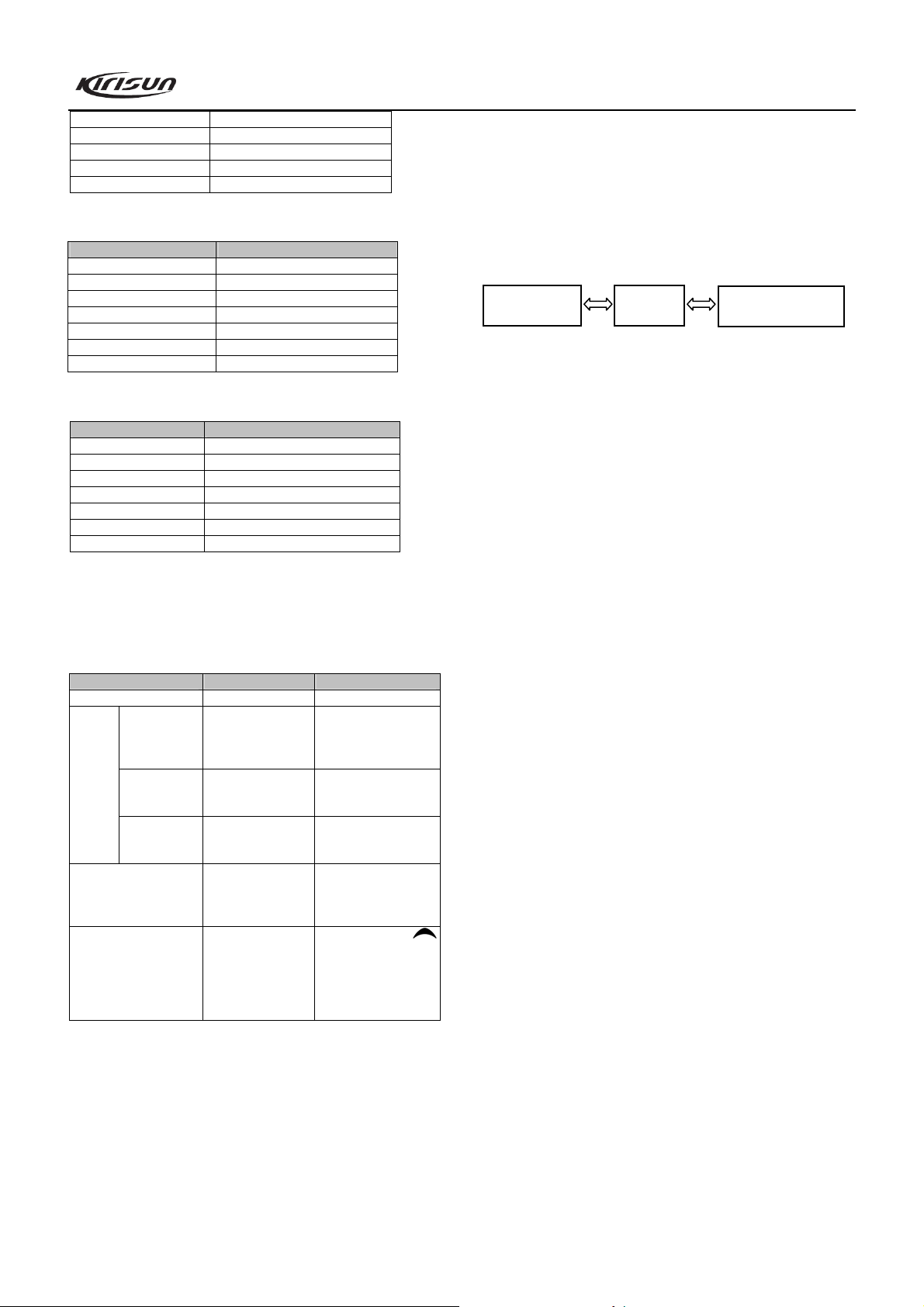
B. Connect the mobile radio to the serial port of the PC with
the special programming cable. Refer to the figure below.
PC
(RS232 Serial Port)
Programming
Cable
Radio (MIC/Programming
Interface)
Figure 5.1
C. Turn the computer power ON.
D. Turn the radio power ON.
E. Run the KSP8100 programming software by double
clicking on its executive program.
F. Click “Program” in the main menu of KSP8100, and click
“Read from radio” in the pull-down menu to read parameters of
the radio to the computer; click “Write to radio” in the pull-down
menu to write parameters in the computer to the radio.
G. The following parameters can be set by using KSP8100
according to requirements of the user:
1) Functions of programmable buttons
2) Alert tone
3) Optional functions
4) 2Tone/DTMF/5Tone signalling
5) TOT
6) Emergency alarm
7) Personal template
8) Scan/FCS/Vote functions
9) Channel information
Please refer to the “Help” document of KSP8100 for details.
Note:
1. Please turn the radio power off before connecting it to the PC.
2. While reading data from the mobile radio, the LED on the
radio lights red, and the PTT key should not be pressed; while
writing data to the mobile radio, the LED on the radio lights
green.
3. Please firstly read data of the radio and back up the data before
editing the parameters on KSP8100.
4. If the radio cannot function normally after being written in
with the edited data, please rewrite the backup data into the radio.
5. “Model Information” is important for the radio; users should
not modify it.
6. After the programming is finished, the mobile radio will restart
automatically and return to the user mode.
5.2 PC Test Mode
9
Page 12

PT8100 Service Manual
Connect the radio to the serial port of the computer with the
special programming cable. Refer to Figure 5.1.
Warning: Before entering the PC Test Mode, please firstly
connect a 50 HF load to the antenna connector of the radio or
connect the radio to a general test set.
With the KSP8100 programming software, you can enter the
Tuning Mode under PC Test Mode to tune the following
parameters of the radio:
1) Frequency
2) Low/Mid/High power
3) Tone Deviation
4) DTMF Deviation
5) DCS Balance
6) DCS Deviation
7) CTCSS (67) Deviation
8) CTCSS (151.4) Deviation
9) CTCSS (254.1) Deviation
10) Rx Sensitivity
11) SQL9/SQL1 On
12) SQL9/SQL1 Off
13) RSSI Level1/Level4
5.3 Firmware Programming Mode
The radio is equipped with an internal Flash ROM which can
be upgraded when new features are released. The operation
procedures are as follows:
1. Turn the radio power ON and the radio enters User Mode.
2. Run the firmware programming software KMU on PC.
3. Connect the radio to the computer by the programming cable.
4. Select a COM port and proper baud rate (115200 is
recommended) according to the actual situation. Then click on
“E.P” to start downloading. The LCD will display “Firmware”.
5. After the communication ends successfully, click on “OK” to
exit.
6. If you want to continue programming other radios, repeat steps
1 to 5.
Chapter 6 Disassembly and Assembly for
Maintenance
The radio is a kind of sophisticated communication
equipment with precise structure and small size. You should
assemble and disassemble it carefully during the maintenance.
The instructions for the assembly and disassembly are as follows.
6.1 Exploded View
28
26
27
26
25
24
23
19
22
21
20
19
Front Cabinet Assembly
面壳组件装配
29
30
19
31
32
33
34
35
12
13
14
15
16
17
18
6
No. Part No. Description PCS
201-008100-R02A
1
203-007200-R08
2
204-008200-R08A
3
4
201-008100-R05A
5
301-25050J-R01C
6
201-008100-R01A
7
204-008000-R01A
8
121-100000-R19
9
120-400000-R14
10
120-400000-R15
11
Volume Knob
Nut for Knob
LCD Protective Film
LOGO
Light Guide
Screw M2.5*5
Front Cabinet
Dustproof Net for Speaker
Speaker
Speaker Wire
Flat Cable
Upper Dustproof Strip for
12 204-008000-R02A
Front Cabinet
Lower Dustproof Strip for
13 204-008000-R03A
203-008000-R02B
14
120-100000-R42A
15
201-008100-R03A
16
203-008000-R03A
17
Front Cabinet
Al Top Case
Power Cable
Power Cable Fastener
Metal Baffle Plate
Rubber Plug for External
18 202-008200-R02A
Speaker Jack
Screw M3*10, with Spring
19 303-30100G-R01
203-008200-R03B
20
102-304452-R01
21
203-008200-R05A
22
204-008200-R10B
23
24
301-30060G-R01
25
Washe r
Antenna Connector
Power Module
Shield for Power Module
Electric Conductive Sponge
Main Board Assembly
Screw M3*6
10
1
2
3
4
5
6
7
8
9
10
11
1
1
1
1
1
6
1
1
1
1
1
1
1
1
1
1
1
1
5
1
1
1
1
1
7
Page 13

PT8100 Service Manual
26 204-008000-R04A
203-008000-R01B
27
301-30250D-R01
28
201-008100-R04A
29
202-008100-R01A
30
203-008100-R01A
31
32 202-008000-R03A
33 202-008100-R02A
34
302-26060D-R01
35
6.2 Instruction for Disassembly of the Radio for Maintenance
6.2.1 RF-PCB disassembly
① Screw off the six M3*25 screws on the Al bottom case, and
remove the Al bottom case (See figure below).
② Screw off the two screws for power module and then remove
the shield for power module. Then remove the solder of the
power module on the PCB with a soldering iron (See figure
below).
③ Screw off the four M2.5*5 screws on the baffle plate, and then
remove the metal baffle plate, the power cable fastener and the
rubber plug for external speaker jack (See figure below).
Dustproof Strip between Top
and Bottom Al Case
Al Bottom Case
Screw M3*25
Lens
Rubber Key
Metal Dome
Heat Conductive Rubber
Cushion
LCD Dustproof Rubber
Cushion
PCB Assembly
Screw M2.6*6
2
1
6
1
1
1
1
1
1
3
6.2.2 Key-PCB disassembly
① Screw off the six M3*25 screws on the Al bottom case, and
remove the bottom case (See figure below).
② Remove the flat cable and speaker wire (See figure below).
③ Screw off the two M2.5*5 screws on the front cabinet, and
then separate the front cabinet from the main machine (See figure
below).
④ Remove the flat cable and the speaker wire, and then remove
the solder between the antenna connector and the RF-PCB with a
soldering iron. Screw off the screws, and take the RF-PCB out of
the top Al case carefully (See figure below).
④ Pull out the volume knob, and then remove the circlip and nut
for volume knob (See figure below).
⑤ Screw off the three fixing screws (M2.6*6) for Key-PCB, and
then take the Key-PCB out of the plastic front cabinet (See figure
below).
After the disassembly above, you can repair and adjust the
radio according its actual malfunction.
11
Page 14

PT8100 Service Manual
Chapter 7 Adjustment
Before test/adjustment, make sure all equipment has been
well grounded!
Before test/adjustment, make sure the antenna output terminal
has been correctly connected to corresponding equipment or
load!
The transmitter output terminal must be terminated with an
RF power attenuator and connected to a standard signal generator
(SSG)/frequency counter/deviation meter/spectrum analyzer!
Make sure no transmission operation is being conducted
while measuring the receiver!
During the adjustment/test/maintenance, make sure reliable
anti-static measures are taken for human body and equipment.
7.1 Equipment and Software Required for Test and
Adjustment
Equipment and software listed in Table 7.1 are required for
test and adjustment of PT8100.
Table 7.1 Equipment and Software Required for Test and
Adjustment
No. Item Specifications
1 Computer
Programming
2
software
Programming
3
cable
4 Clone cable KCL02
DC regulated
5
power supply
6 RF power meter
Frequency
7
counter
8 Deviation meter
9 DMM
Audio signal
10
generator
RF power
11
attenuator
Standard signal
12
generator
13 Oscilloscope
Audio frequency
14
voltmeter
Recommendation: Item 6, 7, 8, 10, 11, and 12 listed in the
table can be replaced by HP8920 general test set.
P2 or above, IBM compatible PC, WINDOWS
98/ME/2000/XP Operating System
KSP8100
KSPL05
Output voltage: 13.8V
Output current: 20A
Measurement range: 0.5-50W
Frequency range: 100MHz-500MHz
Impedance: 50
SWR 1.2
Frequency range: 0.1 - 600MHz
Frequency accuracy: better than ±1×10⁻⁶
Sensitivity: better than 100mV
Frequency range: DC - 600MHz
Measurement range: 0 - ±5kHz
Input impedance: above 10M/V DC, capable of
measuring voltage, current and resistance.
Frequency range:2-3000Hz
Output level: 1-500mV
Attenuation: 40dB or 50dB
Supporting power : higher than 50W
Frequency range: 10MHz-1000MHz
Output level: 0.1uV-32mV (-127dBm~-17dBm)
Frequency range: DC~20MHz
Test range: 10mV-20V
Test range: 10mV-10V
18
81
(CM)
1
(HOOK)
2
(MIC)
3
(ME)
4
5
6
7
8
(PTT)
(GND)
(PSB)
(MBL)
Figure 7.1 External Microphone Interface Definition
7.2 Adjustment
After changing components during the maintenance, it is
necessary to test the radio and adjust its technical parameters. The
following part is going to introduce the adjustment items.
Some parameters can be adjusted by use of KSP8100
programming software (in the Tuning Mode). The adjustable
parameters are as follows:
7.2.1 VCO
a. Adjust the channel to its high frequency point (See Table 7.2).
b. Under the receiving status, measure the voltage of PD by
DMM. Then adjust the PD voltage to be 3.5V ± 0.3V by tuning
the trimming capacitor C122.
c. Under the transmitting status, measure the voltage of PD by
DMM. Then adjust the PD voltage to be 3.5V ± 0.3V by tuning
the trimming capacitor C39.
d. Adjust the channel to its low frequency point (See Table 7.2).
e. Under the receiving status, measure the voltage of PD by
DMM, the value should be larger than 0.6V.
f. Under the transmitting status, measure the voltage of PD by
DMM, the value should be larger than 0.6V.
Table 7.2 High/Center/Low Frequency Point for PT8100
Low Freq Point Center Freq Point High Freq Point
PT8100-01 136.125MHz 154.125MHz 173.975MHz
PT8100-02 400.125MHz 425.125MHz 449.975MHz
PT8100-03 438.125 MHz 464.125 MHz 489.975MHz
7.2.2 Tx deviation (set the HP8920 to be in the Tx status, and set
the filter to be 50Hz~15kHz)
a. Input audio signal of 120mV, 1000Hz to the MIC jack of the
radio.
b. Set the channel to its low frequency point (See Table 7.2).
c. Press and hold the PTT key while adjusting VR2 to make the
deviation be 4.2kHz.
d. Observe the deviation of other channels, which should be
larger than 3.5kHz.
12
Page 15

PT8100 Service Manual
7.2.3 PLL frequency (set the HP8920 to be in the Tx status)
In the “Tuning Mode”, double click “Frequency Stability”,
and adjust the value within the range of 0~255 to make the Tx
frequency reach the rated value (within ±100Hz).
7.2.4 Tx power (set the HP8920 to be in the Tx status)
a. In the “Tuning Mode”, double click “Tx High Power”, and
adjust the five frequency points of “Lowest”, “Low”, “Mid”,
“High” and “Highest” respectively within the range of 0~255 to
make the Tx power be 22W. Meanwhile, observe the operating
current, which should be no larger than 7A.
b. In the “Tuning Mode”, double click “Tx Mid Power”, and
adjust the five frequency points of “Lowest”, “Low”, “Mid”,
“High” and “Highest” respectively within the range of 0~255 to
make the Tx power be 10W. Meanwhile, the operating current
should be no larger than 5A.
c. In the “Tuning Mode”, double click “Tx Low Power”, and
adjust the five frequency points of “Lowest”, “Low”, “Mid”,
“High” and “Highest” respectively within the range of 0~255 to
make the Tx power be 5W.
7.2.5 DCS waveform balance (set the HP8920 to be in the Tx
status, and set the filter to be 20Hz ~ 300Hz)
a. In the “Tuning Mode”, double click “DCS Balance”, select
wideband, and adjust the five frequency points of “Lowest”,
“Low”, “Mid”, “High” and “Highest” respectively within the
range of 0~255 to make the waveform be similar to good square
wave.
b. In the “Tuning Mode”, double click “DCS Balance”, and select
narrowband. Adjust the value within the range of 0~255 to make
the waveform be similar to good square wave.
7.2.6 DCS Deviation (set the HP8920 to be in the Tx status, and
set the filter to be 20Hz ~ 300Hz)
a. In the “Tuning Mode”, double click “DCS Deviation”, and
select “Wideband”. Adjust the five frequency points of “Lowest”,
“Low”, “Mid”, “High” and “Highest” respectively within the
range of 0~255 to make the deviation be 0.75kHz.
b. In the “Tuning Mode”, double click “DCS Deviation”, and
select “Narrowband”. Adjust the value within the range of 0~255
to make the deviation be 0.35kHz.
7.2.7 QT (67) Deviation (set the HP8920 to be in the Tx status,
and set the filter to be 20Hz ~ 300Hz)
a. In the “Tuning Mode”, double click “QT(67) Deviation”, and
select “Wideband”. Adjust the five frequency points of “Lowest”,
“Low”, “Mid”, “High” and “Highest” respectively within the
range of 0~255 to make the deviation be 0.75kHz.
b. In the “Tuning Mode”, double click “QT(67) Deviation”, and
select “Narrowband”. Adjust the value within the range of 0~255
to make the deviation be 0.35kHz.
7.2.8 QT (151) Deviation (set the HP8920 to be in the Tx status,
and set the filter to be 20Hz ~ 300Hz)
a. In the “Tuning Mode”, double click “QT(151) Deviation”, and
select “Wideband”. Adjust the five frequency points of “Lowest”,
“Low”, “Mid”, “High” and “Highest” respectively within the
range of 0~255 to make the deviation be 0.75kHz.
b. In the “Tuning Mode”, double click “QT(151) Deviation”, and
select “Narrowband”. Adjust the value within the range of 0~255
to make the deviation be 0.35kHz.
7.2.9 QT (254) Deviation (set the HP8920 to be in the Tx status,
and set the filter to be 20Hz ~ 300Hz)
a. In the “Tuning Mode”, double click “QT(254) Deviation”, and
select “Wideband”. Adjust the five frequency points of “Lowest”,
“Low”, “Mid”, “High” and “Highest” respectively within the
range of 0~255 to make the deviation be 0.75kHz.
b. In the “Tuning Mode”, double click “QT(254) Deviation”, and
select “Narrowband”. Adjust the value within the range of 0~255
to make the deviation be 0.35kHz.
7.2.10 Tone Deviation/DTMF Deviation (set the HP8920 to be in
the Tx status, and set the filter to be 50Hz ~ 15kHz)
a. In the “Tuning Mode”, double click “Tone Deviation/DTMF
Deviation”, and select “Wideband”. Adjust the five frequency
points of “Lowest”, “Low”, “Mid”, “High” and “Highest”
respectively within the range of 0~255 to make the deviation be
3.5kHz.
b. In the “Tuning Mode”, double click “Tone Deviation/DTMF
Deviation”, and select “Narrowband”. Adjust the value within the
range of 0~255 to make the deviation be 1.7kHz.
7.2.11 Rx Sensitivity (set the HP8920 to be in the Rx status)
In the “Tuning Mode”, double click “Rx Sensitivity”, and
adjust the five frequency points of “Lowest”, “Low”, “Mid”,
“High” and “Highest” respectively within the range of 0~255 to
make the sensitivity of each frequency point be the highest.
See Table 7.4 for detailed parameters.
7.2.12 Rx squelch (set the HP8920 to be in the Rx status)
a. In the “Tuning Mode” (input RF signal with the same
13
Page 16

PT8100 Service Manual
frequency as the adjusted frequency point and with the signal
level of -116dBm, audio frequency of 1kHz, and deviation of
3kHz to the antenna connector of the mobile radio), double click
“SQL9 Open”, and select “Wideband”. Choose a frequency point,
and click “Begin”, the programming software will adjust the
value automatically. When the value keeps stable, click “OK”,
the adjustment of that frequency point is completed. Use the
method to adjust the five frequency points of “Lowest”, “Low”,
“Mid”, “High” and “Highest” respectively.
b. In the “Tuning Mode” (input RF signal with the same
frequency as the adjusted frequency point and with the signal
level of -116dBm, audio frequency of 1kHz, and deviation of
1.5kHz to the antenna connector of the mobile radio), double
click “SQL9 Open”, and select “Narrowband”. Choose a
frequency point, and click “Begin”, the programming software
will adjust the value automatically. When the value keeps stable,
click “OK”, the adjustment of that frequency point is completed.
Use the method to adjust the five frequency points of “Lowest”,
“Low”, “Mid”, “High” and “Highest” respectively.
c. In the “Tuning Mode” (input RF signal with the same
frequency as the adjusted frequency point and with the signal
level of -118dBm, audio frequency of 1kHz, and deviation of
3kHz to the antenna connector of the mobile radio), double click
“SQL9 Close”, and select “Wideband”. Choose a frequency point,
and click “Begin”, the programming software will adjust the
value automatically. When the value keeps stable, click “OK”,
the adjustment of that frequency point is completed. Use the
method to adjust the five frequency points of “Lowest”, “Low”,
“Mid”, “High” and “Highest” respectively.
d. In the “Tuning Mode” (input RF signal with the same
frequency as the adjusted frequency point and with the signal
level of -118dBm, audio frequency of 1kHz, and deviation of
1.5kHz to the antenna connector of the mobile radio), double
click “SQL9 Close”, and select “Narrowband”. Choose a
frequency point, and click “Begin”, the programming software
will adjust the value automatically. When the value keeps stable,
click “OK”, the adjustment of that frequency point is completed.
Use the method to adjust the five frequency points of “Lowest”,
“Low”, “Mid”, “High” and “Highest” respectively.
e. In the “Tuning Mode” (input RF signal with the same
frequency as the adjusted frequency point and with the signal
level of -123dBm, audio frequency of 1kHz, and deviation of
3kHz to the antenna connector of the mobile radio), double click
“SQL1 Open”, and select “Wideband”. Choose a frequency point,
and click “Begin”, the programming software will adjust the
value automatically. When the value keeps stable, click “OK”,
the adjustment of that frequency point is completed. Use the
method to adjust the five frequency points of “Lowest”, “Low”,
“Mid”, “High” and “Highest” respectively.
f. In the “Tuning Mode” (input RF signal with the same
frequency as the adjusted frequency point and with the signal
level of -123dBm, audio frequency of 1kHz, and deviation of
1.5kHz to the antenna connector of the mobile radio), double
click “SQL1 Open”, and select “Narrowband”. Choose a
frequency point, and click “Begin”, the programming software
will adjust the value automatically. When the value keeps stable,
click “OK”, the adjustment of that frequency point is completed.
Use the method to adjust the five frequency points of “Lowest”,
“Low”, “Mid”, “High” and “Highest” respectively.
g. In the “Tuning Mode” (input RF signal with the same
frequency as the adjusted frequency point and with the signal
level of -125dBm, audio frequency of 1kHz, and deviation of
3kHz to the antenna connector of the mobile radio), double click
“SQL1 Close”, and select “Wideband”. Choose a frequency point,
and click “Begin”, the programming software will adjust the
value automatically. When the value keeps stable, click “OK”,
the adjustment of that frequency point is completed. Use the
method to adjust the five frequency points of “Lowest”, “Low”,
“Mid”, “High” and “Highest” respectively.
h. In the “Tuning Mode” (input RF signal with the same
frequency as the adjusted frequency point and with the signal
level of -125dBm, audio frequency of 1kHz, and deviation of
1.5kHz to the antenna connector of the mobile radio), double
click “SQL1 Close”, and select “Narrowband”. Choose a
frequency point, and click “Begin”, the programming software
will adjust the value automatically. When the value keeps stable,
click “OK”, the adjustment of that frequency point is completed.
Use the method to adjust the five frequency points of “Lowest”,
“Low”, “Mid”, “High” and “Highest” respectively.
7.2.13 Rx RSSI (set the HP8920 to be in the Rx status)
a. In the “Tuning Mode” (input RF signal with the same
frequency as the adjusted frequency point and with the signal
level of -116dBm, audio frequency of 1kHz, and deviation of
3kHz to the antenna connector of the mobile radio), double click
“RSSI Level1”, and select “Wideband”. Choose a frequency
point, and click “Begin”, the programming software will adjust
the value automatically. When the value keeps stable, click “OK”,
the adjustment of that frequency point is completed. Use the
method to adjust the five frequency points of “Lowest”, “Low”,
“Mid”, “High” and “Highest” respectively.
b. In the “Tuning Mode” (input RF signal with the same
14
Page 17

PT8100 Service Manual
frequency as the adjusted frequency point and with the signal
level of -116dBm, audio frequency of 1kHz, and deviation of
1.5kHz to the antenna connector of the mobile radio), double
click “RSSI Level1”, and select “Narrowband”. Choose a
frequency point, and click “Begin”, the programming software
will adjust the value automatically. When the value keeps stable,
click “OK”, the adjustment is completed.
c. In the “Tuning Mode” (input RF signal with the same
frequency as the adjusted frequency point and with the signal
level of -80dBm, audio frequency of 1kHz, and deviation of
3kHz to the antenna connector of the mobile radio), double click
“RSSI Level4”, and select “Wideband”. Choose a frequency
point, and click “Begin”, the programming software will adjust
the value automatically. When the value keeps stable, click “OK”,
the adjustment of that frequency point is completed. Use the
Table 7.3 VCO
Item Test Condition Test Equipment
Setting BATT terminal voltage: 13.8V DMM PD
CH: Rx high freq point C122 3.5V ± 0.3V Adjust
VCO lock
voltage
Item Test Condition Test Equipment
BPF
Audio
Power
Sensitivity
Squelch
CH: Rx low freq point
CH: Tx high freq point C39 3.5V ± 0.3V Adjust
CH: Tx low freq point
General test set
Test freq: Mid freq point
Antenna connector input:
RF OUT: -47dBm (1V)
MOD: 1kHz
DEV: ± 3.0kHz/± 1.5kHz
Audio load: 8
CH: Mid freq point
CH: Low freq point
CH: High freq point
RF OUT: -119dBm
(0.25V)
MOD: 1kHz
DEV: ± 3.0kHz/± 1.5kHz
CH: Rx mid freq point
SQL9 Open
RF OUT: -116dBm
SQL9 Close
RF OUT: -118dBm
SQL1 Open
RF OUT: -123dBm
SQL1 Close
RF OUT: -125dBm
Oscilloscope
General test set
Table 7.4 Receiver Section
Spectrum
analyzer /
RF signal
generator
Audio
frequency
voltmeter
Distortion
meter
method to adjust the five frequency points of “Lowest”, “Low”,
“Mid”, “High” and “Highest” respectively.
d. In the “Tuning Mode” (input RF signal with the same
frequency as the adjusted frequency point and with the signal
level of -80dBm, audio frequency of 1kHz, and deviation of
1.5kHz to the antenna connector of the mobile radio), double
click “RSSI Level4”, and select “Narrowband”. Choose a
frequency point, and click “Begin”, the programming software
will adjust the value automatically. When the value keeps stable,
click “OK”, the adjustment is completed.
7.3 Adjustment Description
Refer to Table 7.3, 7.4, and 7.5 for the above mentioned
adjustment.
Measurement
Ter min al
Measurement
Ter min al
Before mixing
Speaker
connector
Adjustment Parts Requirement Remark
﹥0.6V Observe
﹥0.6V Observe
Adjustment
Parts
Tuning
mode
Tuning
mode
Tuning
mode
Tuning
mode
Requirement Remark
User
Smooth wave
(Turn the
volume knob
clockwise to
the end) Audio
power > 4W
SINAD: 12dB
or higher
Normal squelch
open after
adjustment
adjustment not
recommended
15
Page 18

PT8100 Service Manual
Table 7.5 Transmitter Section
Item Test Condition Test Equipment
Tx frequency
DCS waveform
(balance)
Power
Max. modulation
DEV
DTMF DEV Tuning mode
CTCSS DEV CTCSS: 67Hz Tuning mode
CTCSS DEV
CTCSS DEV
DCS DEV DCS: 023N
CH: Tx low freq
point
AG:
1kHz/120mV
CTCSS:
151.4Hz
CTCSS:
254.1Hz
Chapter 8 Specifications
8.1 General Specifications
Product Model PT8100
136-174MHz 400-450MHz Frequency
438-490MHz 350-400MHz
Type of Modulation 16KF3E/11KF3E
Number of Channels 256
Channel Spacing 25kHz/12.5kHz
IF 1st IF: 49.95MHz; 2nd IF: 450kHz
Operating Voltage 13.8V, cathode grounded
Operating
Temperature
Antenna Impedance 50
MIC Impedance 2.2k
Dimension 150*43*131mm (radio only)
Weight 1070g (radio only)
8.2 RX Part
Usable Sensitivity (12dB SINAD) -118dBm
Squelch Open Sensitivity -121dBm @ SQL1
Rx Residual Output W: -45dB; N: -40dB
Modulation Rx Bandwidth W: ± 7kHz; N: ± 3.5kHz
Adjacent Channel Selectivity W: 70dB; N: 60dB
Intermodulation Rejection 65dB
Spurious Response Rejection 70dB
Audio Output Power 4W, balanced @
Rx Current Consumption 1A
Standby Current 100mA
8.3 TX Part
Tx Power 20W/5W @ 13.8V DC
-30℃~ +60℃
Frequency counter
/ General test set
Oscilloscope /
General test set
Power meter /
General test set
Ammeter
Deviation meter /
General test set
distortion 5%, 8
Measurement
Ter min al
Antenna
Frequency Stability ± 2.5ppm
Max. Modulation Deviation ± 5kHz / ± 2.5kHz
Modulation Distortion (300-3000Hz) 3%
Adjacent Channel Tx Power W: 70dB; N 60dB
Spurious Emission 70dB
Residual FM W: -45dB; N: -40dB
Tx Current Consumption 7A @ 13.8V DC
No. Problem Causes and Solutions
1 Power on
2 PLL
3 Cannot
16
Adjustment
Parts
Tuning mode Within ± 100Hz
VR1
Tuning mode Adjust to 22W/5W
VR2
Tuning mode
Tuning mode
Tuning mode
Requirement Remark
Smooth and similar to
square wave
Adjust to ±
4.2kHz/2.1kHz
Adjust to
±3.5kHz/1.7kHz
Adjust to ±
0.75kHz/0.35kHz
Chapter 9 Troubleshooting
A. The power cable is not reliably connected
Failure
unlocked
(Beeping)
transmit
with the accumulator or the radio, please
reconnect it. Make sure the power voltage
should be larger than 13V.
B. The fuse of the power cable is burnt out.
Please change it.
C. The power button is in poor contact. Please
change the rubber key or change the key
PCB.
D. The accumulator is out of power. Please
charge it or change a new one.
E. The MCU is broken, please change the IC.
F. The zener diode IC17 is broken, please
change the IC.
A. The PLL crystal oscillator X1 is broken. Please
change it.
B. The oscillator transistor is broken. Please
change it.
D. The PLL IC3 is broken. Please change it.
A. The frequencies of both users are not the
same. Please select the same frequency
± 200Hz
± 50Hz
Page 19

PT8100 Service Manual
channel again.
B. The CTCSS/DCS signals of both users are
not the same. Please reset it.
C. The radio is out of effective communication
range.
4 No signal A. The antenna is in poor contact. Please fasten
the antenna until secure.
B. The sensitivity is low; please adjust it in the
“Tuning Mode”.
C. The high-frequency amplifying tube Q18 is
broken. Please change it.
D. The squelch level is too high and the squelch
cannot be opened. Please reset the squelch level.
E. The mixing tube Q19 is broken. Please
change it.
F. The FM processing chip IC16 is broken.
Please change it.
5 The
transmitting
red light is
on, but no
voice is
A. Power module IC1 is broken, so there is no
power output, please change it.
B. The microphone is broken, please change it.
C. The operational amplifier IC13 is broken,
please change it.
heard by the
recipient.
6 The
receiving
green light is
on, but no
voice is
heard.
A. The speaker is broken. Please change it.
B. The audio power amplifier IC7 is broken.
Please change a new IC.
C. The switching tube Q33 is broken, please
change a new one.
D. The operational amplifier IC9 is broken,
please change a new IC.
7 Abnormal
programmin
g
A. The programming cable connection is
abnormal, check the cable connection.
B. The RS-232 serial port output of the
computer is abnormal, please check the
computer.
AMP: Amplify, Amplifier
ANT: Antenna
APC: Automatic Power Control
BPF: Band Pass Filter
CTCSS: Continuous Tone Control Squelch System
DCS: Digital Code Squelch
DEMOD: Demodulation
2
E
PROM: Electrical Erasable Programmable Read Only Memory
HPF: High Pass Filter
IDC: Instantaneous Deviation Control
IF: Intermediate Frequency
LED: Light-Emitting Diode
LNA: Low Noise Amplifier
LPF: Low Pass Filter
MCU: Micro Control Unit
MIC: Microphone
MOD: Modulation
MONI: Monitor
PLL: Phase Lock Loop
PTT: Push-to-talk
RX: Receiver
SPK: Speaker
TCXO: Temperature Controlled Crystal Oscillators
TX: Transmitter
UL: Un-lock
VCO: Voltage Control Oscillator
C. The radio’s socket for programming cable is
in poor contact, please check the socket. If
the socket is abnormal, please change it.
Appendix 2 Electronic Parts List
No. Part No. Description Qty Position Mark
1 101-08100V-R04 PT8100PCB / FR4, 1.6mm, PT8100V-100325.PCB, ROHS 1
2 102-0MB90F-R01 CPU / MB90F882PMC-GE1,LQFP100,FUJITSU, ROHS 1 IC11
3 102-1509GV-R01 Frequency Divider IC / UPB1509GV, ROHS 1 IC19
4 102-301317-R01 power modules / RA30H1317M, ROHS 1 IC1
5 102-9124NR-R01 Reset IC / SYSTEM,RESET, PST9124NR,ROHS 1 IC14
6 102-A31136-R01 IF(FM) demodulation IC / TA31136FN,SSOP, ROHS 1 IC6
7 102-AT24C5-R01 Memory IC / AT24C512BN-SH25, ROHS 1 IC12
8 102-B15E03-R01 PLL IC / MB15E03SL,PLL,16-PIN,SSOP, ROHS 1 IC3
9 102-FP3502-R01 Voltage regulator IC / XC62FP3502PR,SOT-89, ROHS 1 IC2
10 102-HT9172-R01 DTMF decode IC/ HT9172,SOP, ROHS 1 IC5
11 102-L7808C-R01 Voltage regulator IC / L7808CV, ROHS 1 IC16
12 102-M2902V-R01 Operational amplifier / NJM2902V,OP-AMP, ROHS 4 IC8, IC9, IC10, IC13
13 102-M2904V-R01 Operational amplifier / NJM2904V,OP-AMP, ROHS 1 IC4
14 102-M78L05-R01 Voltage regulator IC / NJM78L05UA,ROHS 1 IC18
15 102-TA7803-R01 Voltage regulator IC / TA78033AF, TOSHIBA, ROHS 1 IC17
16 102-TDA729-R01 AUDIO, AMP IC / TDA7297D,ST, ROHS 1 IC7
17
Appendix 1 Abbreviations
Page 20

PT8100 Service Manual
17 103-00DZ18-R01 Chip Voltage regulator diode / 02DZ18(X.Y), ROHS 1 D35
18 103-0DA221-R01 Chip diode / DA221(ROHM), ROHS 1 D13
19 103-1SS372-R01 Chip switch diode / 1SS372(TOSHIBA), ROHS 1 D32
20 103-1SV278-R01 Chip variable capacitor diode / 1SV278, ROHS 1 D8
21 103-709CER-R01 Chip diode / L709CER, ROHS 4 D3, D11, D36, D37
22 103-A2S111-R01 Chip switch diode / 0603,MA2S111(PANASONIC), ROHS 2 D12, D15
23 103-DAN222-R01 Chip switch diode/ DAN222,(ROHM), ROHS 3 D20, D21, D33
24 103-HSC277-R01 Chip diode / Waveband switch,HSC277(HITACHI), ROHS 2 D2, D19
25 103-HVC376-R01 Chip variable capacitor diode / HVC376B, ROHS 12 D1, D4, D5, D6, D14, D16, D17, D18, D27, D28, D29, D30
26 103-HZU5AL-R01 Chip Voltage regulator diode / HZU5ALL(HITACHI), ROHS 1 D7
27 103-RB706F-R01 Chip switch diode / RB706F-40,SOT-323, ROHS 3 D9, D10, D25
28 103-SM3MA1-R01 diode / DSM3MA1, ROHS 1 D34
29 104-A144EE-R01 Chip transistor / DTA144EE(ROHM), ROHS 4 Q23, Q29, Q35, Q36
30 104-C144EE-R01 Chip transistor / DTC144EE(ROHM), ROHS 14
31 104-KRC404-R01 Chip transistor / KRC404RTK, ROHS 1 Q41
32 104-SA1641-R01 Chip transistor / 2SA1641(S.T),ROHS 1 Q39
33 104-SC3357-R01 Chip transistor / 2SC3357,ROHS 2 Q4, Q5
34 104-SC4116-R01 Chip transistor / 2SC4116-GR,ROHS 1 Q13
35 104-SC4617-R02 Chip transistor / 2SC4617(R)(ROHM),ROHS 6 Q8, Q14, Q21, Q26, Q31, Q52
36 104-SC4919-R01 Chip transistor / 2SC4919,MUTING,CIRCUIT(SANYO),ROHS 1 Q32
37 104-SC5108-R01 Chip transistor / 2SC5108Y(TOSHIBA),ROHS 5 Q1, Q2, Q7, Q11, Q20
38 104-TA1298-R01 Chip transistor / KTA1298(Y),ROHS 2 Q38, Q40
39 105-2SK508-R01 Chip FET(field-effect transistor) / 2SK508NV(K52),ROHS 2 Q6, Q12
40 105-3SK318-R01 Chip FET(field-effect transistor) / 3SK318,ROHS 2 Q18, Q19
41 105-SK1824-R01 Chip FET(field-effect transistor) / 2SK1824,ROHS 9 Q3, Q30, Q33, Q34, Q45, Q46, Q49, Q53, Q54
42 107-008200-R01 PT8200 LCD / 8200 LCD ,ROHS 1
43 108-450C24-R02 Chip phase frequency detector / JTBM450CX24,ROHS 1 CD1
44 108-CF450F-R01 Plug-in porcelain filter / LTM450FW,450kHz±7kHz, ROHS 1 CF2
45 108-CF450H-R01 Plug-in porcelain filter / LTM450HT,450kHz±3kHz, ROHS 1 CF1
46 108-XF4995-R01 plug-in IF filter / 49.95MHz±7.5KHz,U-5*2,ROHS 1 XF1, XF2
47 109-040000-R01 Chip resistor / 0402,0R±5%,ROHS 31
48 109-040100-R01 Chip resistor / 0402,10R±5%,ROHS 5 R2, R3, R71, R82, R266
49 109-040101-R01 Chip resistor / 0402,100R±5%,ROHS 5 R21, R26, R101, R121, R247
50 109-040102-R01 Chip resistor / 0402,1K±5%,ROHS 16
51 109-040103-R01 Chip resistor / 0402,10K±5%,ROHS 28
52 109-040104-R01 Chip resistor / 0402,100K±5%,ROHS 13
53 109-040105-R01 Chip resistor / 0402,1M±5%,ROHS 8 R130, R131, R133, R137, R139, R192, R277, R312
54 109-040121-R01 Chip resistor / 0402,120R±5%,ROHS 1 R61
55 109-040122-R01 Chip resistor / 0402,1.2K±5%,ROHS 2 R152, R267
56 109-040123-R01 Chip resistor / 0402,12K±5%,ROHS 2 R16, R245
57 109-040124-R01 Chip resistor / 0402,120K±5%,ROHS 2 R150, R175
58 109-040151-R01 Chip resistor / 0402,150R±5%,ROHS 2 R63, R111
59 109-040152-R01 Chip resistor / 0402,1.5K±5%,ROHS 2 R54, R218
60 109-040153-R01 Chip resistor / 0402,15K±5%,ROHS 2 R162, R272
61 109-040154-R01 Chip resistor / 0402,150K±5%,ROHS 8 R6, R11, R27, R168, R181, R216, R223, R226
62 109-040183-R01 Chip resistor / 0402,18K±5%,ROHS 5 R198, R207, R217, R259, R320
63 109-040184-R01 Chip resistor / 0402,180K±1%,ROHS 5 R92, R117, R169, R170, R177
64 109-040204-R01 Chip resistor / 0402,200K±5%,ROHS 1 R69
65 109-040220-R01 Chip resistor / 0402,22R±5%,ROHS 2 R37, R103
66 109-040222-R01 Chip resistor / 0402,2.2K±5%,ROHS 2 R1, R227
67 109-040223-R01 Chip resistor / 0402,22K±5%,ROHS 6 R106, R109, R110, R153, R171, R215
68 109-040224-R01 Chip resistor / 0402,220K±5%,ROHS 3 R183, R213, R311
69 109-040272-R01 Chip resistor / 0402,2.7K±5%,ROHS 3 R57, R148, R222
70 109-040273-R01 Chip resistor / 0402,27K±5%,ROHS 5 R78, R118, R161, R205, R251
71 109-040274-R01 Chip resistor / 0402,270K±5%,ROHS 5 R42, R164, R246, R306, R318
72 109-040331-R01 Chip resistor / 0402,330R±5%,ROHS 2 R14, R43
73 109-040332-R01 Chip resistor / 0402,3.3K±5%,ROHS 5 R124, R142, R146, R159, R211
74 109-040333-R01 Chip resistor / 0402,33K±5%,ROHS 7 R147, R151, R156, R157, R185, R249, R319
75 109-040334-R01 Chip resistor / 0402,330K±5%,ROHS 4 R73, R108, R134, R269
76 109-040361-R01 Chip resistor / 0402,360R±5%,ROHS 1 R299
77 109-040392-R01 Chip resistor / 0402,3.9K±5%,ROHS 1 R279
Q9, Q10, Q17, Q22, Q24, Q25, Q27, Q28, Q37, Q42, Q43, Q44,
Q47, Q50
C134, C135, C374, C375, R17, R66, R68, R72, R84, R85, R86,
R144, R145, R167, R172, R187, R188, R189, R196, R229, R236,
R237, R248, R252, R257, R268, R302, R322, R325, R336, R339
R9, R48, R70, R83, R104, R136, R201, R219, R231, R254, R265,
R270, R292, R297, R315, R338
R10, R12, R13, R15, R24, R35, R62, R65, R74, R79, R81, R112,
R174, R210, R228, R233, R280, R284, R285, R286, R287, R298,
R307, R308, R309, R313, R314, R316
R40, R52, R53, R59, R60, R67, R80, R199, R208, R214, R225,
R230, R239
18
Page 21

PT8100 Service Manual
78 109-040393-R01 Chip resistor / 0402,39K±5%,ROHS 3 R64, R143, R278
79 109-040394-R01 Chip resistor / 0402,390K±5%,ROHS 3 R202, R220, R310
80 109-040433-R01 Chip resistor / 0402,43K±5%,ROHS 1 R163
81 109-040470-R01 Chip resistor / 0402,47R±5%,ROHS 1 R33
82 109-040471-R01 Chip resistor / 0402,470R±5%,ROHS 4 R100, R271, R290, R291
83 109-040472-R01 Chip resistor / 0402,4.7K±5%,ROHS 22
84 109-040473-R01 Chip resistor / 0402,47K±5%,ROHS 16
85 109-040474-R01 Chip resistor / 0402,470K±5%,ROHS 6 R140, R165, R204, R250, R253, R305
86 109-040560-R01 Chip resistor / 0402,56R±5%,ROHS 2 R115, R135
87 109-040561-R01 Chip resistor / 0402,560R±5%,ROHS 2 R51, R55
88 109-040562-R01 Chip resistor / 0402,5.6K±5%,ROHS 7 R155, R178, R184, R193, R212, R241, R260
89 109-040563-R01 Chip resistor / 0402,56K±5%,ROHS 7 R97, R125, R149, R232, R258, R263, R275
90 109-040564-R01 Chip resistor / 0402,560K±5%,ROHS 2 R99, R243
91 109-040682-R01 Chip resistor / 0402,6.8K±5%,ROHS 6 R94, R95, R113, R114, R244, R317
92 109-040683-R01 Chip resistor / 0402,68K±5%,ROHS 3 R194, R264, R274
93 109-040821-R01 Chip resistor / 0402,820R±5%,ROHS 3 R76, R77, R255
94 109-040822-R01 Chip resistor / 0402,8.2K±5%,ROHS 2 R235, R242
95 109-040823-R01 Chip resistor / 0402,82K±5%,ROHS 3 R75, R88, R224
96 109-040913-R01 Chip resistor / 0402,91K±5%,ROHS 2 R190, R209
97 109-040914-R01 Chip resistor / 0402,910K±5%,ROHS 1 R221
98 109-060000-R01 Chip resistor / 0603,0R±5%,ROHS 5 C31, C176, D23, L52, L62
99 109-060100-R01 Chip resistor / 0603,10R±5%,ROHS 1 R8
100 109-060103-R01 Chip resistor / 0603,10K±5%,ROHS 1 R45
101 109-060121-R01 Chip resistor / 0603,120R±5%,ROHS 1 R4
102 109-060152-R02 Chip resistor / 0603,1.5K±1%,ROHS 1 R41
103 109-060220-R01 Chip resistor / 0603,22R±5%,ROHS 1 R30
104 109-060221-R01 Chip resistor / 0603,220R±5%,ROHS 1 L8
105 109-060222-R01 Chip resistor / 0603,2.2K±5%,ROHS 2 R18, R19
106 109-060271-R01 Chip resistor / 0603,270R±5%,ROHS 1 R44
107 109-060274-R01 Chip resistor / 0603,270K±5%,ROHS 1 R36
108 109-060332-R01 Chip resistor / 0603,3.3K±5%,ROHS 1 R32
109 109-060470-R01 Chip resistor / 0603,47R±5%,ROHS 2 R29, R34
110 109-060473-R01 Chip resistor / 0603,47K±5%,ROHS 2 R182, R206
111 109-060561-R01 Chip resistor / 0603,560R±5%,ROHS 2 R22, R23
112 109-060681-R01 Chip resistor / 0603,680R±5%,ROHS 1 R58
113 109-070000-R01 Chip resistor / 0805,0R±5%,ROHS 1 L54
114 109-070220-R01 Chip resistor / 0805,22R±5%,ROHS 1 L30
115 109-070470-R01 Chip resistor / 0805,47R±5%,ROHS 1 L31
116 109-100221-R01 Chip resistor / 1206,220R±5%,ROHS 2 R46, R47
117 110-110503-R01 Chip trimming resistor / EVM2NSX80B54,50K±25%,ROHS 1 VR2
118 111-010000-R01 plug-in piezoresistance / 10D220,ROHS 1 R281
119 111-030000-R07 Chip Resettable Fuse / 1206L150PR,1206,1.5A/6V,ROHS 1 F1
120 111-030000-R09 plug-in glass tube fuse / 313010,32V,10A,ROHS 4
121 112-043100-R01 Chip capacitor / 0402,10P±0.5P,50V,C0G,ROHS 6 C7, C16, C80, C138, C139, C307
122 112-043101-R01 Chip capacitor / 0402,100P±5%,50V,C0G,ROHS 28
123 112-043102-R01 Chip capacitor / 0402,1000P±10%,50V,X7R,ROHS 38
124 112-043103-R01 Chip capacitor / 0402,0.01uF±10%,50V,X7R,ROHS 15
125 112-043104-R02 Chip capacitor / 0402,0.1uF±10%,16V,X7R,ROHS 41
126 112-043105-R01 Chip capacitor / 0402,1uF±10%,6.3V,X5R,ROHS 11
127 112-043123-R01 Chip capacitor / 0402,0.012uF±10%,25V,X7R,ROHS 3 C252, C292, C386
128 112-043150-R01 Chip capacitor / 0402,15P±5%,50V,C0G,ROHS 5 C13, C53, C118, C168, C190
129 112-043151-R01 Chip capacitor / 0402,150P±5%,50V,C0G,ROHS 1 C195
130 112-043153-R01 Chip capacitor / 0402,0.015uF±10%,50V,X7R,ROHS 6 C249, C258, C263, C273, C387, C389
131 112-043181-R01 Chip capacitor / 0402,180P±10%,50V,X7R,ROHS 2 C2, C106
132 112-043182-R01 Chip capacitor / 0402,1800P±10%,50V,X7R,ROHS 3 C154, C158, C217
R5, R38, R39, R91, R128, R154, R158, R173, R176, R179, R180,
R191, R195, R197, R200, R203, R282, R283, R288, R289, R303,
R304
R89, R105, R123, R126, R127, R129, R141, R160, R238, R293,
R294, R300, R328, R331, R333, R337
C27, C28, C97, C103, C105, C108, C112, C114, C125, C335,
C336, C349, C350, C351, C352, C353, C354, C356, C359, C360,
C361, C362, C363, C364, C369, C382, C383, C384
C82, C98, C19, C21, C36, C37, C49, C57, C58, C59, C68, C87,
C89, C90, C91, C92, C95, C99, C167, C170, C171, C188, C189,
C196, C206, C214, C220, C223, C231, C266, C311, C321, C370,
C371, C372, C373, C413, C416
C33, C51, C55, C81, C110, C115, C121, C133, C145, C153, C242,
C284, C330, C333, C385
C17, C23, C24, C83, C102, C144, C172, C173, C183, C184, C186,
C187, C204, C209, C210, C211, C213, C230, C235, C253, C259,
C260, C261, C264, C268, C270, C271, C272, C275, C295, C300,
C308, C312, C319, C325, C329, C334, C337, C338, C394, R296
C56, C120, C254, C280, C298, C303, C304, C323, C367, C378,
C414
19
Page 22

PT8100 Service Manual
133 112-043183-R01 Chip capacitor / 0402,0.018uF±10%,25V,X7R,ROHS 4 C257, C276, C390, C391
134 112-0431R5-R01 Chip capacitor / 0402,1.5P±0.25P,50V,C0G,ROHS 2 C69, C70
135 112-043200-R01 Chip capacitor / 0402,20P±5%,50V,C0G,ROHS 2 C281, C296
136 112-043221-R01 Chip capacitor / 0402,220P±5%,50V,C0G,ROHS 1 C282
137 112-043222-R01 Chip capacitor / 0402,2200P±10%,50V,X7R,ROHS 1 C248
138 112-043223-R01 Chip capacitor / 0402,0.022uF±10%,25V,X7R,ROHS 5 C238, C239, C322, C355, C365
139 112-043270-R01 Chip capacitor / 0402,27P±5%,50V,C0G,ROHS 3 C194, C197, C198
140 112-043273-R01 Chip capacitor / 0402,0.027uF±10%,50V,X7R,ROHS 1 C396
141 112-0432R0-R01 Chip capacitor / 0402,2P±0.25P,50V,C0G,ROHS 2 C104, C201
142 112-043330-R01 Chip capacitor / 0402,33P±5%,50V,C0G,ROHS 5 C6, C93, C130, C147, C232
143 112-043331-R01 Chip capacitor / 0402,330P±10%,50V,X7R,ROHS 1 C140
144 112-043332-R01 Chip capacitor / 0402,3300P±10%,50V,X7R,ROHS 1 C297
145 112-043333-R01 Chip capacitor / 0402,0.033uF±10%,16V,X7R,ROHS 1 C243
146 112-043360-R01 Chip capacitor / 0402,36P±5%,50V,C0G,ROHS 1 C205
147 112-043390-R01 Chip capacitor / 0402,39P±5%,50V,C0G,ROHS 2 C225, C229
148 112-043392-R01 Chip capacitor / 0402,3900P±10%,50V,X7R,ROHS 8 C256, C301, C314, C377, C399, C400, C401, C402
149 112-043393-R01 Chip capacitor / 0402,0.039uF±10%,10V,X7R,ROHS 4 C156, C250, C251, C288
150 112-0433R0-R01 Chip capacitor / 0402,3P±0.25P,50V,C0G,ROHS 3 C124, C177, C291
151 112-043470-R01 Chip capacitor / 0402,47P±5%,50V,C0G,ROHS 2 C129, C255
C3, C9, C11, C12, C20, C38, C47, C52, C54, C71, C76, C88,
C116, C119, C123, C128, C136, C142, C143, C148, C151, C157,
152 112-043471-R01 Chip capacitor / 0402,470P±10%,50V,X7R,ROHS 55
153 112-043472-R01 Chip capacitor / 0402,4700P±10%,25V,X7R,ROHS 1 C262
154 112-043473-R01 Chip capacitor / 0402,0.047uF±10%,16V,X7R,ROHS 3 C287, C294, C306
155 112-043474-R01 Chip capacitor / 0402,0.47uF±10%,10V,X5R,ROHS 1 C267
156 112-0434R0-R01 Chip capacitor / 0402,4P±0.25P,50V,C0G,ROHS 4 C35, C162, C163, C208
157 112-0435R0-R01 Chip capacitor / 0402,5P±0.25P,50V,C0G,ROHS 1 C200
158 112-043681-R01 Chip capacitor / 0402,680P±10%,16V,X7R,ROHS 1 C132
159 112-043682-R01 Chip capacitor / 0402,6800P±10%,16V,X7R,ROHS 1 C299
160 112-043683-R02 Chip capacitor / 0402,0.068uF±10%,10V,X7R,ROHS 7 C236, C240, C357, C358,C244, C245, C320
161 112-0436R0-R01 Chip capacitor / 0402,6P±0.5P,50V,C0G,ROHS 7 C72, C73, C126, C161, C164, C166, C175
162 112-0437R0-R01 Chip capacitor / 0402,7P±0.5P,50V,C0G,ROHS 1 C107
163 112-043820-R01 Chip capacitor / 0402,82P±5%,50V,C0G,ROHS 1 C234
164 112-043821-R01 Chip capacitor / 0402,820P±10%,16V,X7R,ROHS 3 C406, C409, C412
165 112-0438R0-R01 Chip capacitor / 0402,8P±0.5P,50V,C0G,ROHS 2 C165, C192
166 112-0439R0-R01 Chip capacitor / 0402,9P±0.5P,50V,C0G,ROHS 1 C100
167 112-043R50-R01 Chip capacitor / 0402,0.5P±0.1P,50V,C0G,ROHS 5 C48, C60, C61, C65, C127
168 112-063101-R01 Chip capacitor / 0603,100P±5%,50V,C0G,ROHS 1 C18
169 112-063102-R01 Chip capacitor / 0603,1000P±10%,50V,X7R,ROHS 13
170 112-063104-R01 Chip capacitor / 0603,0.1uF±10%,50V,X7R,ROHS 1 C96
171 112-063150-R01 Chip capacitor / 0603,15P±5%,50V,C0G,ROHS 1 C30
172 112-0631R0-R01 Chip capacitor / 0603,1P±0.25P,50V,C0G,ROHS 2 C4, C5
173 112-0635R0-R01 Chip capacitor / 0603,5P±0.25P,50V,C0G,ROHS 1 C34
174 112-0636R0-R01 Chip capacitor / 0603,6P±0.5P,50V,C0G,ROHS 1 C32
175 112-0637R0-R01 Chip capacitor / 0603,7P±0.5P,50V,C0G,ROHS 1 C10
176 112-0638R0-R01 Chip capacitor / 0603,8P±0.5P,50V,C0G,ROHS 1 C75
177 112-063R50-R01 Chip capacitor / 0603,0.5P±0.1P,50V,C0G,ROHS 2 C41, C111
178 112-072105-R01 Chip Ta capacitor/ TP Model, SIZE P,1uF±20%,10V,ROHS 2 C290, C415
179 112-072106-R01 Chip Ta capacitor/ TP Model, SIZE P,10uF±20%, 6.3V, ROHS 1 C327
180 112-072225-R01 Chip Ta capacitor/TP Model, SIZE P,2.2uF±20%, 10V, ROHS 3 C233, C237, C313
181 112-072475-R01 Chip Ta capacitor/TP Model, SIZE P,4.7uF±20%, 10V, ROHS 13
182 112-073334-R01 Chip capacitor/0805,0.33uF+80%--20%,10V,Y5V,ROHS 1 C181
183 112-102104-R01 Chip Ta capacitor/ TS Model, SIZE A, 0.1uF±20%, 35V, ROHS 2 C109, C113
184 112-102105-R01 Chip Ta capacitor/ TS Model, SIZE A,1uF±20%, 16V, ROHS 2 C117, C411
185 112-102156-R01 Chip Ta capacitor/TS Model, SIZE A,15uF±20%, 6.3V, ROHS 2 C137, C149
186 112-102475-R02 Chip Ta capacitor/ TS Model, SIZE A,4.7uF±20%, 16V, ROHS 1 C380
187 112-103100-R02
188 112-103102-R02
189 112-103106-R01 Chip capacitor / 1206,10uF+80%--20%,16V,Y5V,ROHS 1 C265
190 112-103150-R02
Chip monolithic ceramic capacitors / 1206,10P ± 5%,
1000V,C0G,ROHS
Chip monolithic ceramic capacitors / 1206,1000P ±
10%,1000V,C0G,ROHS
Chip monolithic ceramic capacitors / 1206,15P ±
5%,1000V,C0G,ROHS
C160, C169, C174, C178, C182, C207, C212, C215, C218, C221,
C222, C247, C274, C279, C283, C285, C293, C302, C305, C310,
C317, C326, C328, C332, C339, C340, C342, C343, C347, C348,
C392, C395, C405
C22, C25, C26, C64, C67, C77, C78, C79, C84, C85, C86, C101,
R7
C1, C8, C42, C131, C159, C216, C226, C246, C278, C286, C345,
C346, C404
2 C44, C376
2 C29, C403
1 C45
20
Page 23

PT8100 Service Manual
191 112-103180-R02
192 112-103220-R01
193 112-103270-R01
194 112-1032R0-R02
195 112-103300-R02
196 112-1033R0-R02
197 112-1035R0-R01
198 112-1038R0-R02
199 112-191477-R01
200 112-201476-R02
201 113-010100-R01 Chip trimming capacitor / TZV2Z100A110,3~10p+100,ROHS 2 C39, C122
202 114-06E180-R01
203 114-06E330-R01
204 114-06E470-R01
205 114-06E560-R01
206 114-06G102-R01 Chip inductor / MLF1608A1R0K,1uH±5%,0603,ROHS 1 L48
207 114-06G151-R01 Chip inductor / MLF1608DR15K,150nH±10%,0603,ROHS 1 L47
208 114-06G221-R02 Chip inductor / LGHK1608R22J-T,220nH±5%,0603,ROHS 3 L21, L27, L44
209 114-06G332-R01 Chip inductor / MLF1608A3R3K,3.3uH±5%,0603,ROHS 2 L5, L37
210 114-06G471-R01 Chip inductor / MLF1608DR47K,470nH±10%,0603,ROHS 1 L41
211 114-06G561-R01 Chip inductor / MLF1608DR56K,560nH±10%,0603,ROHS 1 L42
212 114-06G680-R01 Chip inductor / MLG1608B68NJ,68nH±5%,0603,ROHS 2 L14, L15
213 114-06G682-R01 Chip inductor / MLF1608E6R8K,6.8uH±10%,0603,ROHS 4 L2, L12, L34, L38
214 114-06G820-R01 Chip inductor / MLG1608B82N,82nH±5%,0603,ROHS 1 L7
215 114-07E180-R01 Chip Wire inductor / C2012C-18NJ,18nH±5%,0805,ROHS 1 L35
216 114-07E270-R01 Chip Wire inductor / C2012C-27NJ,27nH±5%,0805,ROHS 1 L3
217 114-07E390-R01 Chip Wire inductor / C2012C-39NJ,39nH±5%,0805,ROHS 2 L29, L57
218 114-07E470-R02 Chip Wire inductor / C2012C-47NG,47nH±2%,0805,ROHS 1 L58
219 114-07E560-R02 Chip Wire inductor / C2012C-56NJ,56nH±5%,0805,ROHS 1 L55
220 114-08E103-R01 Chip inductor / FSLM2520-100J,10uH±5%,1008,ROHS 1 L40
221 114-08E471-R01 Chip inductor / FSLM2520-R47K,470nH±10%,1008,ROHS 1 L49
222 114-08E821-R01 Chip inductor / FSLM2520-R82K,820nH±10%,1008,ROHS 1 L50
223 115-3R0110-R01
224 115-3R05R0-R05 Chip air-cored coil / 0.9*3.0*4.5TR, positive, ROHS 4 L9, L10, L11, L79
225 115-3R06R0-R02
226 117-000000-R05 Chip bead / EMI,FILTER, SMT,BLM21P300S,0805,ROHS 3 L64, L72, L77
227 117-000000-R07 Chip bead / EMI,FILTER, SMT,BLM41P600SPT,1206,ROHS 2 L25, L26
228 117-000000-R08 Chip bead / EMI,FILTER, SMT,BLM11A601S,0603,ROHS 21
229 119-060104-R01 Thermistor / NTH5G16P42B104K07TH,100K,0603,ROHS 2 R90, R138
230 120-100000-R39C PT8200 Power Line with LV-2A jack, Length=3000mm, ROHS 1
231 120-100000-R42A
232 120-400000-R14 black and white twisted-pair with jack,2.0*2P*70mm, ROHS 1
233 120-400000-R15 flat cable / 0.5*34P*60mm,ROHS 1
234 121-100000-R19 Speaker / 16Ω,7W,SANYO ,ROHS 1
235 122-116M80-R01 Chip TCXO / DSA535SA,16.8MHz±2.5PPm,ROHS 1 X1
236 122-13M580-R02 Chip crystal resonator / 3.58MHz,SMT-49,30PPM,ROHS 1 X2
237 122-19M830-R01 Chip crystal resonator/ 9.8304MHZ-NX5032GA,ROHS 1 X3
238 124-020000-R08 Chip connector / 08 6210 034 340 800, 34PIN, P=0.5mm, ROHS 1 CN4
239 124-050000-R16 3.5mm MIC socket / MOTOROLA, PJ-D3027, DC30V0.5A, ROHS 1 J1
240 124-090000-R01 Speaker socket / WCPW20-02,ROHS 2 CN2, CN3
Chip monolithic ceramic capacitors / 1206,18P ±
5%,1000V,C0G,ROHS
Chip monolithic ceramic capacitors / 1206,22P ±
5%,1000V,C0G,ROHS
Chip monolithic ceramic capacitors / 1206,27P ±
5%,1000V,C0G,ROHS
Chip monolithic ceramic capacitors / 1206,2P ±
5%,1000V,C0G,ROHS
Chip monolithic ceramic capacitors / 1206,30P ± 5%,
1000V,C0G,ROHS
Chip monolithic ceramic capacitors / 1206,3P ± 5%,
1000V,C0G,ROHS
Chip monolithic ceramic capacitors / 1206,5P ± 5%,
1000V,C0G,ROHS
Chip monolithic ceramic capacitors / 1206,8P ± 5%,
1000V,C0G,ROHS
plug-in electrolytic capacitor / Ф 10*16,470UF25V, ±
20%,ROHS
Chip electrolytic capacitor / Φ 6.3*5.3,47U25V, ±
20%,ROHS
Chip Wire inductor / C1608CB-18NJ, ceramic 18NH ±
5%,0603,ROHS
Chip Wire inductor / C1608CB-33NJ, green,ceramic core ,
33NH±5%,0603,ROHS
Chip Wire inductor / C1608CB-47NJ, green,ceramic core47NH
±5%,0603,ROHS
Chip Wire inductor / C1608CB-56NJ, ceramic 56nH ±
5%,0603,ROHS
Chip air-cored coil / 0.9*3.0*11TR,
ROHS
Chip air-cored coil / 0.9*3.0*6TR,
ROHS
PT8000/PT8100 Power Line Unit main, with LV-2A jack and
SR,ROHS
positive, high pin,
positive, high pin,
1 C62
1 C94
1 C43
1 C14
1 C46
1 C63
1 C152
1 C15
1 C331
3 C66, C341, C379
1 L20
2 L13, L45
2 L36, L46
1 L53
1 L19
2 L18, L28
L1, L4, L22, L23, L24, L32, L33, L39, L51, L59, L60, L61,
L65, L66, L67, L69, L70, L74, L75, L76, L78
1
21
Page 24

PT8100 Service Manual
Appendix 3 Structural Parts List
No. Part number Description Unit Qty.
1 201-008100-R01A PT8100 Case Front/ ABS, Black, ROHS pcs 1
2 201-008100-R02A PT8100 Knob Volume / ABS, Black, white sign, ROHS pcs 1
3 201-008100-R03A PT8100 SR Power Line/ ABS, Black, ROHS pcs 1
4 201-008100-R04A PT8100 Lens Display Window / PC, Transparent, ROHS pcs 1
5 201-008100-R05A PT8100 Lens Led / PC, Transparent, ROHS pcs 1
6 202-008000-R03A
7 202-008100-R01A PT8100 Key Rubber / rubber, silkprint, ROHS pcs 1
8 202-008100-R02A PT8100 Dustproof Cushion LCD/ Rubber,45 degree, black, ROHS pcs 1
9 202-008200-R02A PT8200 Plug Speaker Jack/ Rubber, Black, ROHS pcs 1
10 203-00618A-R08 PT618A Handed Microphone Bracket/ with 2pcs Screw(SP4*16), ROHS pcs 1
11 203-007200-R08 PT7200 Nut Volume Knob/ Cu, Zn-Plated, Black, ROHS pcs 1
12 203-008000-R01B PT8000 Case Top / Al, Spray Black Oil, ROHS pcs 1
13 203-008000-R02B PT8000 Case Bottom / Al, Spray Black Oil, ROHS pcs 1
14 203-008000-R03A PT8000 Metal Plate/ SECC, Thk's=1.2mm,Spray Black Oil, ROHS pcs 1
15 203-008000-R04A V8000 Assemble Bracket/ SUS304,Spray Black Oil, ROHS pcs 1
16 203-008100-R01A PT8100 METAL DOME,ROHS pcs 1
17 203-008200-R03B PT8200 Base Antenna / SL16-50KF-3,Plated Gold, ROHS pcs 1
18 203-008200-R05A PT8200 Shield Cover Power Module/Cu, Ni-Plated, ROHS pcs 1
19 204-008000-R01A PT8000 Dustproof Net Speaker/Black, ROHS pcs 1
20 204-008000-R02A PT8000 Dustproof Strip Case Front Top/ with Tape, Black, ROHS pcs 1
21 204-008000-R03A PT8000 Dustproof Strip Case Front Bottom/ with Tape, Black, ROHS pcs 1
22 204-008000-R04A PT8000 Dustproof Case Al/ with Tape, Black, ROHS pcs 2
23 204-008000-R06A PT8000/8100 Washer Sponge/ Sponge,60*38*10mm,ROHS pcs 1
24 204-008200-R08A PT8200 Film LCD Lens/ 0.1mm PVC,ROHS pcs 1
25 204-008200-R10B PT8200 Conductive Sponge/ 50*18.5*3,with Tape, ROHS pcs 1
26 301-25050J-R01C Screw/ M2.5*5.0,Black Zn-Plated, ROHS pcs 6
27 301-30060G-R01 Screw/ M3.0*6.0,Black Zn-Plated, ROHS pcs 7
28 301-30250D-R01 Screw/ M3.0*25.0,Black Zn-Plated, ROHS pcs 6
29 302-26060D-R01 Screw/ SP2.6*6.0,Black Zn-Plated, ROHS pcs 3
30 302-50160E-R01 Screw/ SP5.0*16.0,Ni-Plated,ROHS pcs 4
31 303-30100G-R01 Screw/ M3.0*10.0,with Flat and Spring Washer, Ni-Plated, ROHS pcs 5
32 303-40100D-R01 Screw/ M4.0*10.0, with Flat and Spring Washer, Black Zn-Plated, ROHS pcs 4
Item Model Specifications External View
Mounting Bracket
Power Cable
PT8000/8100 Washer Transmit Thermal / Rubber, Black, 3*7*15mm, HC240,
ROHS
Appendix 4 Accessories
pcs 1
Hand Microphone KME215
Microphone Hanger
SEMS Screw M4.0*10.0
Self-tapping Screw M5.0*16.0
Self-tapping Screw M4.0*16.0
22
Page 25

PT8100 Service Manual
Figure 1 PT8100 Block Diagram
D D
GLED LCD RST LCD BLC LCD WR
TXD
AF_MUTE
1
LCD RD DEV2 DEV1 CKLEDT RX SCL TEST
AFCO MAXAFSHIFT
W/N RLED
TXGSW
PA
MIC_MUTE
8TC8RC SBC
RXD
IGN
TONEIN
TEMP
INT
PTT
UL
C C
RSSI BUSY
DV
MICDAT HOOK
SDA
RESET
EXT-ALARM
QT/DQT IN
D0D1D2D3
B B
QT TCXO
16.8MHz
TCXO
X1
*3 2ND LOCAL AMP
Q11
8R
3.5V
A A
CK
DT
UL
UL
MB15E03SL
PLL IC
IC3
1
5V
MB90F882
CPU
AT24C512
EEPROM
IC12
2
3
5C
3V
NJM78L05UA
4
IC18
8R
8RC
Q40
SW
IC11
X3
9.8304MHz
KEY BOARD
P1P2POWER
P3P4P5
450KHz
CF2
MOD
5T
IC13D IC13AIC13BIC13C
LP LP IDC AMP
8TC
Q38
SW
Q8
HP
Q52
HP
AMP LP LP AMP
IC9C IC9BIC9AIC9D
AMP HP LP LP
BUSY
D25
DET
NOISE
AMP
Q21
5V
IF DEMODULATOR
450KHz
CF1
IF AMP
8R
IC8A IC8BIC8CIC8D
MIX
8R
5V
RIPPLE
FILTER
Q14
AF OUT
IC6
5V
DET COLL
450KHZ
CD1
Q20
49.95MHz
XF1
Q19
LOOP FILTER
BUFF
Q7
5V
VCO
VCO
Q14
Q6
TX
RX
MOD
BUFF
Q1 Q2
DIVIDER
IC19
5V
RF AMP
5V
TX/RX SW
RF AMP
Q4
8T
DRIVE
Q5
PRE
8T
2
3
8T 8R
4
RA30H
HP
TA78033AF
IC17
5
Title
Date: 2010-4-15 Sheet of
File: C:\Documents and Settings\..\PT8000 BLOCK DEAGRAM.SchDocDrawn By:
A3
Number RevisionSize
6
BATTARY
13.8V
TA7808S
IC16
DECODER
DTMF
IC10BIC10A
AMP
IC5
2T
D0D1D2D3DV
MUTE
Q33
SW
VR1
10K
TDA7297D
MIC
SPEAKER
CTCSS/DCS
Q26
HP
8R
AF POWER AMP
IC7
J1 SPK
BPF
Q18
MIX
8R
8T
BPF
APC CONTROL
IC4
APC
IC1
ANT SW
5
LPF
TO ANT
6
23
Page 26

PT8100 Service Manual
Figure 2 PT8100 Main Board Schematic Circuit Diagram
D D
R303
C335
C336
C349
C350 101
C351
C352 101
C353 101
CN4
CN34
C354
C356 101
1
GND
MD
HOOK
ME
MIC
ME
PTT
NC
SB
NC
GND
AFIN
AFOUT
GND
MD0
MD2
3M
POWER
P1
P2
P3
P4
P5
RXL
TXL
L_RST
L_BLC
5C
5C
L_DA
L_WR
L_RD
L_CS
GND
35
C359 101
C360 101
C361 101
C362 101
C363 101
C364 101
C369 101
C382 101
2
C383 101
C384 101
3
4
Prepare:
Check:
5
Approve:
Page:
6
4.7K
101
101
101
101
101
1
2
3
4
5
6
7
8
SB
9
10
11
12
13
14
15
16
17
18
19
20
21
22
23
24
25
26
27
28
5C
29
30
31
32
33
34
DTC144EE
R292
1K
C348 471
C347
471
02DZ18<X.Y>
470R
Name:
File No:
MAIN BOARD SCH PT8100-01(136-174MHz)
Model Name:
REV:
Scale:
Q44
R325 0R
DTC144EE
DTC144EE
KRC404RTK
D35
R291
R282
4.7K
BLM11A601S
L65
R187
BLM11A601S
L22
C272
104
C275
104
C278
4.7uF/10V
C230
104
C204
104
C24
0R
MD
HOOK
ME
MIC
PTT
R302
0R
R188
0R
TXD
AFIN
AFOUT
MD0
MD2
POWER
P1
P2
P3
P4
P5
RXL
TXL
L_RST
L_BLC
L_DA
L_WR
L_RD
L_CS
SBC
8RC
8TC
C337
104
Q38
KTA1298
Q43
R288
4.7K
R284
10K
C338
104
Q40 KTA1298
R285 10K
R289
4.7K
8C
4.7uF/10V
C345
C339
471
IC16 L7808CV
OUTIN
C340
471
SB
C341
47uF/25V
Q39 2SA1641
Q42
R290
470R
R283
C346
4.7uF/10V
4.7K
C342
471
IC17 TA78033AF
Q41
OUTIN
C343
471
B3M
F1
1.5A
C329
104
C330
103
L72
BLM21P300S
IGN
Q48
*
C219
*
C318
*
R295
*
R261 *
R281
10D220
D34
DSM3MA1
470uF/25V
C331
C332
471
C333
103
C334
104
DC1
13.8V
+
-
104
C76
471
R200
4.7K
1
8
A0
VCC
R20647K
2
7
A1
TEST
R230
100K
3
6
A2
SCL
R219 1K
5
GND4SDA
IC12
?
T7
MARKERT8MARKER
QT IN
W/N
C404
4.7uF/10V
L77
BLM21P300S
104
R214
100K
C405
471
5C
R211
3.3K
IC18 NJM78L05UA
R226
150K
OUTIN
R218
1.5K
C289
*
R222
2.7K
R227 2.2K
R223
150K
4.7K
105
C368
103
A-MU
AFIN
MAX
2TIN
AFOUT
Q35
DTA144EE
PA
W/N
BLM11A601S
C328 471
C327
10uF/6.3V
M-MU
MIC
2TOUT
APCO
E-ALA
1K
C312
104
R293
47K
MAX AF:L
DTC144EE
R294
47K
R268
0R
R262
*
C311
102
C317
471
L68
*
R270
1K
2SK1824
R273 *
R264
C323 105
R275
56K
68K
C314
392
C412
821
R276
*
R272
15K
C310
471
14
L70
A+in
B+in
Aout
A-in
V+
4
1
2
3
R278
39K
R263
56K
C322
R267 1.2K
R277
1M
223
R279
C320
C308
104
683
3.9K
C321
102
C319
104
R274
68K
C313
2.2uF/10V
C326
471
R271
470R
TX MUTE:H
820R
C325
104
BLM11A601S
L69
C316*
CN3
R182
47K
4.7K
Q47
R2605.6K
Q34
56K
18K
5
RXL
2TIN
TO0
R180
4.7K
100
98
99
NC
TONEIN
1
TXL
NC
2
NC
3
NC
4
NC
5
P5
POWER
6
P1
P1
7
P2
P2
8
P3
P3
9
P4
P4
10
POWER
P5
11
GLED
12
TEST
RLED
13
VCC
14
VSS
15
C23 104
C
16
L_RST
LCD RST
17
L_BLC
LCD BLC
18
L_DA
LCD DAT
19
L_WR
LCD WR
20
L_RD
LCD RD
21
L_CS
SCL
LCD CS
22
MD
MICDAT
23
HOOK
SDA
HOOK
24
DEV2
DEV2
25
DEV1
DEV1
CK
UL
LE
26
27
28
UL
CK
LE
TXD
INT
RXD
MD0
MD2
T3
T1
3
TXDT6VCCT4RXDT5RESET
MD0T2MD2
C315*R301
OUT
3
*
IC15
*
OUT1VDD2GND
4
C300 104
NC4NC
5
C302 471
R287
10K
R286
10K
C393
*
R228
10K
R224
82K
R220
390K
100K
R225
C264
C287473
393
333
R203
C254
0R
R258
R259
2SK1824
R2570RR248
C306 473
C307
123
C290 1uF/10V
W:H N:L
C250
393
DTA144EE
150K
R168
Q8
2SC4617(R)
R197
510K
R221
R144
0R
R166
*
C293
471
C251
C243
R181 150K
L67
BLM11A601S
R167 0R
Q52
2SC4617(R)
C394
104
R243
560K
R254
R336
0R
Q33
R31610K
C392
471
Q46
2SK1824
L66
BLM11A601S
C395
471
R317
6.8K
R315 1K
Q31
2SC4617(R)
C304
Q45 2SK1824
105
R252
R2311KR239
100K
R251
27K
R236
100K
0R
C298
105
C303
105
R234
*
R229
0R
R300
47K
C301
392
R337
47K
R232
56K
R321 *
C294
473
C305
471
R241
5.6K
W:H N:L
IC13NJM2902V
Cout8C-in9C+in10GND11D+in12D-in13Dout
W:H N:L
Bout
B-in
7
6
BLM21P300S
SB
R24512K
R249
33K
Q30
2SK1824
10P
C295
104
R244
6.8K
D32
1SS372
R237
0R
100R
R247
R240
*
C396273
C299
682
D33
DAN222
R255
R242
8.2K
Q32 2SC4919
R2358. 2K
C297
332
R256*
CN5
CN2
APC
XOUT
XIN
TO1
W/N
TV
QT/DQT IN
AVRH
AVCC
BUSY36TEMP
AVSS
RSSI
NC
DT
34
33
32
29
31
35
30
QT IN
BUSY
RSSI
DT
R266
10R
L51
BLM11A601S
9.8304MHz
IC14 PS T9124NR
NC1VEE12VEE2
VCC
5
R269330K
L63
*
C285
471
4.7uF/10V
C286
R207
18K
R198
18K
C282 221
7
GND
C+in
Cout
C-in
8
9
10
11
R208 100K
C284 103
C288 393
R199
100K
R21010K
R217
C279 471
18K
R204 470K
1M
R192
R209 91K
Q29
C267
105
150K
R216
Cout8C-in9C+in10GND11D+in12D-in13Dout
B+in
Bout
B-in
V+
3
4
1
2
R215
22K
C273
123
R213
220K
R202 390K
C276
333
333
R193
5.6K
91K
R212
5.6K
C280
105
C390
183
C391
183
Cout8C-in9C+in10GND11D+in12D-in13Dout
A+in
Aout
A-in
V+
7
4
6
5
R313
10K
1M
R312
R314 10K
R307
10K
R310
390K
R311
220K
C270
104
R196 0R
R205
27K
0r-16r
0R
C277
*
DTC144EE
2SK1824
Q50
C374
0R
Q49
2SK1824
47K
C375
0R
C265
10uF
C268
104
C274
471
C411
1uF/16V
L64
Q28
DTC144EE
68K
C283
471
2
R2011K
112
R238
47K
SPEAKER ON:L
C269
*
1
2
CN2
C C
R176 4.7K
R179 4.7K
R333 47K
R334 *
R335 *
IGN
E-ALA
M-MU
APCO
MAX
SHIFT
PTT
R132
*
R128
4.7K
R17
84
82
IGN83EXT-ALARM
MAXAF85NC86SHIFT87VCC88VSS89X190X091NC92NC93W/N94APC95TV96DCSTCXO97DCSVCO
DTMFD043DTMFD144DTMFD245DTMFD3
VSS
NC38NC39NC40NC
41
42
37
TEMP
D0
D1D2D3
XOUT
XIN
C281
20P
C29620P
R265
1K
Q27
DTC144EE
X3
C291
3P
R185 33K
L75
47P
C255
BLM11A601S
R183
220K
R171
22K
IC8 NJM2902V
Aout1A-in2A+in3V+4B+in5B-in6Bout
D+in
Dout
D-in
14
13
12
C266 102
C252
123
D31 *
C261
104
C26222 2
C256
103
R184
5.6K
R173
3.3K
R178 5.6K
123
14
IC9 NJM2902V
A+in
Aout
A-in
7
6
5
C263 123
C258
123
R174
10K
C257
R175
120K
R190
R172 0R
Q26
2SC4617(R)
C253 104
C389
153
R308
10K
C387
153
14
IC10 NJM2902V
B+in
Bout
B-in
1
2
3
R309 10K
R304 4.7K
C386
123
103
C367
105
C415
1uF/10V
R339
Q54
47K
C409
821
C271
104
R105
PW GND10PW GND
9
STAND-BY
8
MUT
7
IN1
6
VCC
5
OUT-
4
NC
R194
3
NC
2
OUT1+
1
PW GND
R332
*
C410
*
R330
*
C408*
J1 SPK
0R
78
76
R28
*
MIC_MUTE77APCO
P01
NC79NC80NC81PTT
75
P00
74
VCCN
VCCN
73
2TOUT
DTMF
72
NC
71
NC
70
A-MU
AF_MUTE
69
PA
PA
68
TGSW
TXGSW
67
SBC
SBC
66
8RC
8RC
65
8TC
8TC
64
DVSS
63
DVCC
62
INT
INT
61
D0
NC
60
D1
NC
59
D2
NC
58
D3
TXD
TXD
57
RXD
DV
RXD
56
NC
55
TEST
TEST
54
SDA
SDA
53
SCL
SCL
52
RESET
RESET
DTMFDV
51
TO1
MD0
MD0
MD249MD1
RX
R122
*
50
47
46
48
RX
DV
SHIFT
C246
4.7uF/10V
C244
683
R170 180K
R169 180K
C248 222
C245
473
C249
R164
270K
R165
470K
C247
471
R306270 K
C292 123
R305
470K
C385
R331
OUT2-
OUT2+
PWGND
TDA7297D
TO0
MD2
IC11
MB90F882
R38
4.7K
Q24
DTC144EE
RSSI
APC
DEV1
DEV2
TV
RESET
VR2
50K
Q25
DTC144EE
R163
43K
C242
103
3.3K
Q23
DTA144EE
2.7K
R152
1.2K
CD1
C24450
C235
104
R318
270K
R253 470K
R250 470KR246 27 0K
Q53
2SK1824
C259104
R328
47K
C406
821
11
12
NC
13
SGND
14
IN2-
15
VCC
16
17
NC
18
NC
R157
33K
19
C239
223
20
R156
33K
C238
223
IC7
R327
*
R329
*
C324
*
C407
*
1
2
CN3
CN2
C225
39P
C229
39P
X2
3.58MHz
R139
1M
9
DV
OE
D011D112D213D3
14
10
R151
33K
C357
683
C358
683
R191
4.7K
R195 4.7K
C236
683
C240
683
R186
*
R158
4.7K
R154
4.7K
R189
0R
VR1
*
15K
R162
C241
*
R149
56K
120K
R150
R153
22K
C233
2.2uF/10V
R160
47K
R161
27K
R155
5.6K
2.2uF/10V
C237
R159
471
W:L N:H
C227 *
C224
*
L62 0R
C231
102
R177
180K
R142
R146
3.3K
C370
3.3K
R233
10K
R148
102
9
FILI8AF
7
10
FILO
QUAD
6
11
R140470K
DEC
IFO
5
12
IFI
RSSI
C234
82P
4
13
VCC
NDET
3
14
MIXOUT
NREC
2
15
XOUT
GND
1
16
XIN
MIXI
182
IC6
TA31136
C232
33P
102
C226
4.7uF/10V
39K
R143
R141
47K
R319
33K
102
C365
223
R147
33K
C220 102
C355
223
15
C222
471
HVC376B
C223
R137 1M
EST
4.7uF/10V
R138 100K
1K
C221 471
C218
C21
D30
HVC376B
C215
471
VP1VN2GS3VREF4INH5PWDN6X17X28VSS
RT/GT
VDD
17
16
330K
C216
104
56R
R136
R1450R
C217
BLM11A601S
D29
HVC376B
1M
1M
L61 BLM11A601S
C214
102
D28
HVC376B
D27
B B
3M
47K
R126
R127
47K
IC5 HT9172
18
R134
C210104
C183
104
R116
*
R106
22K
C211
104
BLM11A601S
C184
104
L60
R296
104
C366
R129
47K
C213
102
R135
3.3K
*
Q22
DTC144EE
C212 4 71
104
L59
471
56K
R130
R131
R133 1M
C208 4P
*
R112
10K
R322
0R
L76 BLM11A601S
BUSY
W/N
C181
334
T
C189
102
104
C206
R124
C228
102
R119
*
R120
*
C209
R121 100R
C190
15P
C191
*
C1928PR107
C193
*
C207
R125
R117
180K
C197
27P
C202 *
C198
27P
C203 *
C200 5P
C195
151
C196
102
R123 47K
R118
27K
C194
27P
47nH
L58
C205 36P
C201 2P
L57 39nH
C199 *
R280
10K
D25
RB706F-40
Q37
DTC144EE
Q36
DTA144EE
C187
Q21 2SC4617(R)
R108
330K
C188
R109 22K R110 22K
R113
6.8K
CF2450KHz F
R114 6.8K
471
Q20
2SC5108
*
*
C185
*
*
R111
150R
104
C186
L55
56nH
0R
L56
*
R115
56R
0R
W:H N:L
Q17
DTC144EE
R338
1K
C120
105
W:L N:H
C56
105
W:H N:L
C172
104
D20
DAN222
R94 6.8K R95 6.8K
CF1
450KHz HT
D21
DAN222
C173
104
2LO
L48 1uH
C182
*
R102
560K
R99
C170
102
C179
R100
470R
49.95MHz
XF1
49.95MHz
XF2
R101
100R
C180
C171
102
R91
4.7K
L50
0.82uH
0.47uH
L49
R92
180K
R97
56K
Q19
3SK318
C167
102
C166
6P
C178
471
L47
150nH
RSSI
R93
*
D22
*
R96
*
C175
6P
Q16
*
R98
*
D23
C176
0R
C169
471
L53
56nH
R104
1K
R103
22R
Q18
3SK318
L52
C174
471
C177
3P
L54 0R
C168
15P
VCCN
C132
681
L39
BLM11A601S
R76
820R
C158 182
C143
471
R71
10R
C144
104
C154
182
R78 27KR7782 0R
C145
103
4.7uF/10V
C131
R88
82K
1
4
VC
VCC
C159
4.7uF/10V
2
3
16.8MHz
GND
OUT
R84
0R
X1
16.8MHz
C155
*
R85
0R
C138
10P
C156
393
L40
10uH
R86
0R
R70
1K
C139
10P
C129
47P
C150
*
R69
200K
Q11
2SC5108
560nH
L42
C142
R82 10R
471
C133 103
L41
470nH
C140
331
C146 *
C1340RL43
*
C147 33P
C130
33P
L44
220nH
C135 0R
C141
*
2LO
RX
C165
8P
C163
4P
C164
6P
TGSW
TEMP
16.8*3 MHz
D18
HVC376B
C127
0.5P
C148
471
Q12 2SK508NV(K52)
15uF/6.3V
C149
R74
Q14 2SC 4617(R)
10K
471
C151
Q13 2SC4 116
C153
103
0R
C137
15uF/6.3V
R68
C128
471
DTC144EE
C400
C402
C401
BLM11A601S
392
392
L74
392
392
TX:H RX:L
D19 HSC277
C161
6P
33nH
C162
4P
47nH
C160
471
47K
T
100K
C399
L45
L46
TX:L TX OFF:H
R89
R79
10K
R83
1K
R75
82K
R90
471
C157
R81 10K
R87
*
R73
330K
C136
471
Aout1A-in2A+in3GND
R80 100K
Bout
B-in
V+
8
7
6
R72
0R
C416
102
A A
*
C114 101
R50 *
C105
101
*
C112
101
C103
101
1K
C108
101
16
IC3
MB15E03SL
OSCOUT
OSCIN
1
2
R66
0R
C116
471
C113
0.1uF/35V
R54 1.5K
R55
560R
R57
2.7K
C117
1uF/16V
R51
560R
C109
0.1uF/35V
BLM11A601S
L33
C125 101
L34
6.8uH
D17
HVC376B
HVC376B
HVC376B
D16
D14
C106
180P
L38 6.8uH
C118
15P
C122
10P
L35
18nH
C124
3P
C107
7P
104
L37 3.3uH
C126
6P
C123
471
R61 120R
102
BLM11A601S
C111 0.5P
R65
10K
R62 10K
Q10
C377
392
R58 680R
C101
102
DA221
Q9
DTC144EE
C102104
R63
150R
C37947uF/25V
C121
103
C99
102
C110
103
C115
103
102P
22P
R52
100K
C119
471
R59100K
R67
100K
R53
100K
MA2S111
D15
4
R64
39K
IC4 NJM29 04
C152
R60 100K
B+in
5
C104
2P
C1009PL36
47nH
R10 10K
R15 10K
R24 10K
R35 10K
UNLOCK:0V
R49
D12
MA2S111
R48
100K
R40
VCC
DO
VP
4
5
3
R37
22R
C88
471
BLM11A601S
L23
R39
4.7K
R42
270K
270K
102
C96
104
R44 270RL27 220nH
C95
L32
C89
102
R45 10K
1.5K
R41
D13
47R
L31
L24
BLM11A601S
R43
330R
C92 102
C97 101P
L25
L26
BLM41P600SPT
R46 220R
C98
R47 220R
C94
102
L28
6T
L709CE
5P
D11
102
L709CE
D36
39nH
L29
C93
33P
C9 471
1
IC2
XC62FP3502
OUTIN
3.5V
C1 4.7uF/10V
R11 150K
BLM11A601S
C11
471
L4
C12
471
CLOCK9DATA10LE11PS12ZC13LD/FOUT14P/15R/
R2 10R
C20
471
XFIN
GND
FIN
C8 4.7uF/10V
8
6
7
C58
102
C72 6P
C73 6P
Q7
2SC5108
150K
C80 10P
TX OR RX H:4.0V
C69
1.5P
R36
C70
1.5P
C87
C71
471
C83
C68
102
102
C413
102
R299
360R
R33
47R
471
R32
C77 102
C84 102
3.3K
47R
L3022R
C85 102
C67
102
C75
C78 102
C86 102
R34 47R
22R
102
C79
102
4.7uF/16V
C74
NC
47uF/25V
C82102PC81 103
C90
D10
RB706F-40
D9 RB706F-40
C91
C42 4.7uF/10V
C52
471
L20
18nH
15P
C53
33nH
R27
D6 HVC376B
1SV278
D8
L21 220 nH
Q6
2SK508NV(K52)
R26 100R
*
R20
105
C57
102
C59
R21
100R
UPB1509GV
SW15SW2
L78
BLM11A601S
R13
10K
C49
102
*
C50
R16
C54
12K
L16
*
L17
R31*R7 102
*
R25 *
R29
R18
2.2K
68nH
8P
R30
R19
2.2K
68nH
C64
*
R22 560R
R23 560R
C380
D7 HZU5ALL
C51
103
C55 103
C66
C45
15P
C46
30P
L18
6T
C403
102
C376
10P
0.5P
C65
0.5P
27P
18P
C60
0.5P
0.5P
10P
*
L19
11T
L1 B LM11A601S
R3
10R
C3 471
C33 103
C17 104
C35 4P
L13
C38 471
1K
D5
HVC376B
HVC376B
C41 0.5P
L12 6. 8uH
C39 10P
6P
C34 5P
C47
471
10K
C378
105
102
4
R14
330R
102
L14
L15
C40
10R
C36
102
C37 102
5T
D37
L709CE
102
5T
C48
C43
5T
C62
C61
5T
C44
C381
TO ANT
2
R9
C18
101
L2
6.8uH
HVC376B
D4
D1
C2
180P
C16
10P
27nH
L3
C32
C10 7P
L5 3 .3uH
R4 120R
C4 1P
Q3 2S K1824
C414
C5 1P
R12
3
Q1
2SC5108
R6
150K
L8
220R
C6
33P
C13 15P
C371
IC19
VCC11IN2IN-3GND
VCC2
OUT
7
8
6
R297
1K
C372
102
C373102
R298
10K
2SC5108
Q2
R1
2.2K
L7
82nH
C7 10P
4
R5
4.7K
D2
HSC277
C19
102
C22 102
C25
Q4
2SC3357
C30 15P
Q5
2SC3357
C31 0R
L6
*
5
C26 102
IC1 RA30H1317M
R8
PIN
C27 101P
VGG
C28 101P
VDD
POUT
L10
D3
L709CE
C29
C14
2P
L9
C15
8P
L11
6
C63
3P
L79
CN1
ULLEDT
CK
R56
24
Page 27

PT8100 Service Manual
Figure 3 PT8100 Main Board Top Layer Position Mark Diagram
25
Page 28

PT8100 Service Manual
Figure 4 PT8100 Main Board Top Layer Position Value Diagram
26
Page 29

PT8100 Service Manual
Figure 5 PT8100 Main Board Bottom Layer Position Mark Diagram
27
Page 30

PT8100 Service Manual
Figure 6 PT8100 Main Board Bottom Layer Position Value Diagram
28
Page 31

PT8100 Service Manual
Figure 7 PT8100 Key Board Schematic Circuit Diagram
D D
1
C3
101
C4
*
C5
0
1
FLASH
CN34
35
34
33
32
31
30
29
28
27
26
25
24
23
22
21
20
19
18
17
16
15
14
13
12
11
10
9
8
7
6
5
4
3
2
1
CN2
0R
MD2MD0
MODE
101
C6
101
C7
*
C8
101
F1
1812L110PR
C13
101
C14
101
C15
101
C16
101
C17
101
C12
101
R27
6.8K
R22
1K
R23
1K
R30
6.8K
SW2
MOD0
MOD2
R36
SW1
R14
*
K1 P1
R15
*
K2 P2 K3 P3
R16
*
K4 P4 K5 P5 K6 POWER
R6
*
R9
*
R10
*
2
GND
MD
3
File No:
Prepare:
Check:
4
5
HOOK
ME
MIC
ME
PTT
NC
SB
NC
GND
AFIN
AFOUT
GND
MD0
MD2
3M
POWER
P1
P2
P3
P4
P5
RXL
TXL
L_RST
L_BLC
5C
5C
KEY BOARD SCH(M:R03)Name:
L_DA
L_WR
L_RD
L_CS
GND
1
6
REV:
Approve:
Page:
7
0 NORMAL
Model Name:
PT8100
C C
CN1 RJ45
GND
BLC
B
7
8
R26 220R
C27 101
C28 101
R21
*
D13
1DZ1-MA8039
C10 101 C29 101 C30 101
C31 101 C32 101
R8 6.8K
R7 6.8K
R5 6.8K
R32 6.8K
R29 6.8K
R28 6.8K
C33 101
HOOK
MIC
PTT
6
MD
ME
4
5
2
1
3
R11 220R
R12 220R
R13 0R
DTC144EE
C26
471
C22 *
C23 101
C24 101
C25 *
C21
101
D11
1DZ1-MA8039
D12
1DZ1-MA8039
R18
0R
*
R33
6.8K
C18
471
Q2
DTC144EE
R24
220R
D15
3RG9HWA
R25
220R
Q3
DTC144EE
C19
471
R34
6.8K
B B
R1 330R
R2
D3
YELLOW
D1
YELLOW
D2
YELLOW
330R
VR1
10K
D4
YELLOW
D6
YELLOW
D5
YELLOW
Q1
R31
0R
BLM11A601S
L4
C36
471
R19
*
R20
*
R3
0R
R17
R4
100R
CN3
CN10
10
NC
9
NC
8
RST
7
LED
6
VDD
5
VSS
4
DA
3
WR
2
RD
1
CS
A A
1
2
C2 *
IC2 *
OUTIN
C1 *
C20
*
3
4
5
6
7
Scale:
8
8
29
Page 32

PT8100 Service Manual
Figure 8 PT8100 Key Board Top Layer Position Mark Diagram
30
Page 33

PT8100 Service Manual
Figure 9 PT8100 Key Board Top Layer Position Value Diagram
31
Page 34

PT8100 Service Manual
Figure 10 PT8100 Key Board Bottom Layer Position Mark Diagram
32
Page 35

PT8100 Service Manual
Figure 11 PT8100 Key Board Bottom Layer Position Value Diagram
33
 Loading...