

Page 1
PT8000
SERVICE MANUAL
VHF/UHF MOBILE RADIO
V071215
Page 2

PT8000 SERVICE MANUAL
DANGEROUS!!
Do not connect AC power or the DC power that
exceeds the specified input value with any
connector or terminals of the radio. Otherwise it will
cause fire or electric shock.
WARNING!
Do not reverse power connection.
It may cause harm to the radio if signal input on the
antenna connector is bigger than 20 dBm (100mW).
Do not turn on the power before the antenna or load
connection is completed.
If the antenna has been damaged, do not use the radio.
Damaged antenna may cause tightly burning on skin.
CONTENTS
Chapter 1 Introduction.......................................................................2
Chapter 2 Radio Overview.................................................................3
Chapter 3 Circuit Introduction............................................................3
Chapter 4 Mode Introduction.............................................................7
Chapter 5 Maintenance, Assembly and Disassembly........................8
Chapter 6 Overall Debugging..........................................................10
Chapter 7 Main T echnical Indexes...................................................13
Chapter 8 Trouble Shooting Guide..................................................13
Appendix 1 Abbreviations................................................................14
Appendix 2 Electronic components list............................................14
Appendix 3 Framework components list..........................................18
Appendix 4 Accessories..................................................................19
Appendix 5 PT8000 Spare Mechanical Part BOM...........................20
Figure 1 PT8000 Schematic Circuit Diagram...................................21
Figure 2 PT8000 Main Board Schematic Circuit Diagram................22
Figure 3 PT8000 T op Main Board Position Mark Diagram...............23
Figure 4 PT8000 Bottom Main Board Position Mark Diagram..........24
Figure 5 PT8000 Keyboard Schematic Diagram............................. 25
Figure 6 PT8000 T op Keyboard Position Mark Diagram..................26
Figure 7 PT8000 Bottom Keyboard Position Mark Diagram............27
It's better to avoid putting it in rain or snow, or any other
liquid to ensure its life and performance.
STATEMENT!
Kirisun Electronic (Shenzhen) Co., Ltd owns the copyright
of KSP8000 software.
Unauthorized Duplication of KSP8000 software is strictly
prohibited.
Kirisun Electronic (Shenzhen) Co., Ltd owns the copyright
of the MCU software.
Kirisun Electronic (Shenzhen) Co., Ltd owns the copyright
of the radio outward/structure/circuit design.
Kirisun Electronic (Shenzhen) Co., Ltd owns the copyright
of this service manual. Unauthorized publication is
prohibited.
Kirisun Electronic (Shenzhen) Co., Ltd owns the
trademarks KIRISUN , , .
1
Page 3
PT8000 SERVICE MANUAL
Chapter 1 Introduction
Installation Condition
1.Unpack
1.1 Introduction
This manual applies to the service and maintenance of PT8000 series of
FM mobile radio, and is designed for the engineers and professional
technicians that have been trained by our company. In this manual you
can find all the information of product service. Kirisun reserves the rights
to modify the product construction and specification without notice in
order to enhance product performance and quality. You can also log on
our website www.kirisun.com to download the latest service manual or
contact your local dealer or us.
Read this manual before repair the product.
1.2 Service Precautions
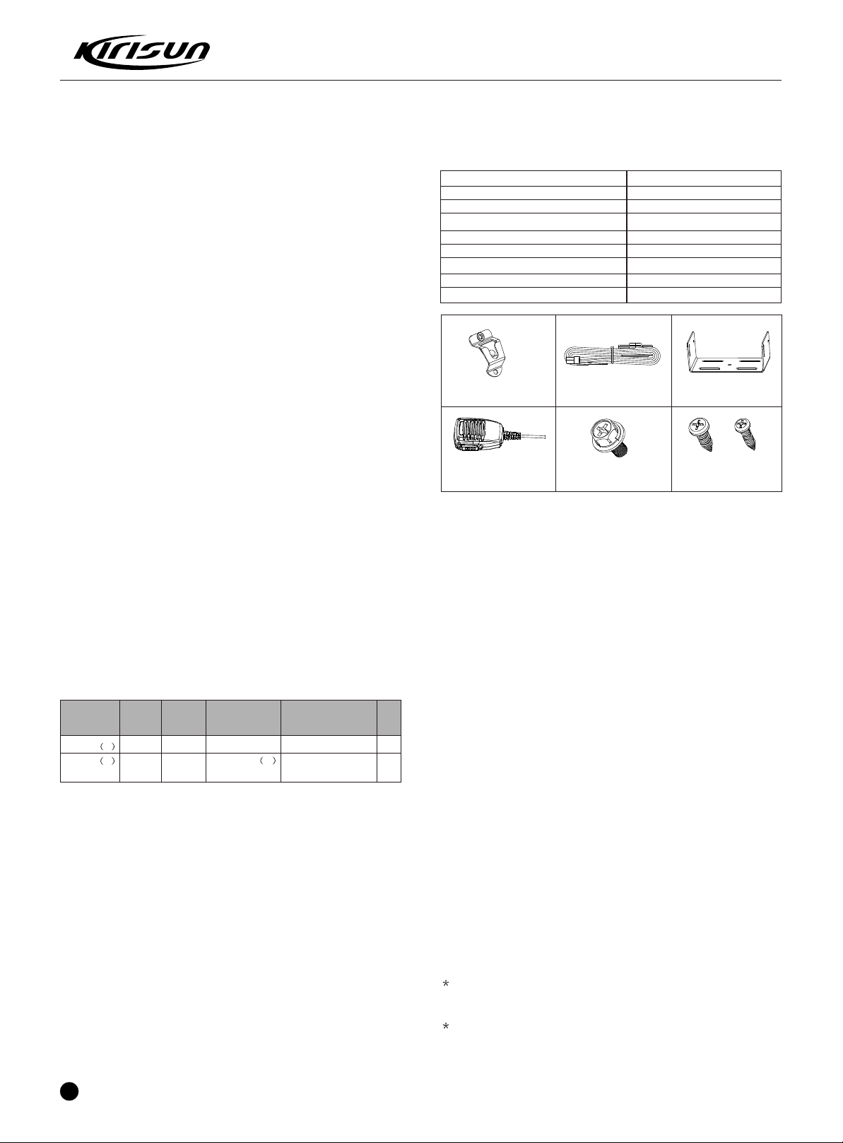
Please check the host in the package and the supplied accessories in
the following table before using. Any articles are found lost or damaged,
please contact the distributor without delay.
Accessories
Fixed bracket
Power Cable
Hand Microphone
Microphone Hanger
M4*10 Combination Screw
M4*16 Self-tapping Screw
M5*16 Self-tapping Screw
Instruction Manual
Quantity
1
1
1
1
4
2
4
1
Safety
Avoid skin contacting with the antenna connector and PCB.
Do not reverse the power polarities.
If signal input is bigger than 20dBm (100mW) it may cause damage to
the radio.
Do not turn on the power before the antenna and load connection is
Microphone Hanger
Power Cable
Fixed bracket
completed.
Do not use the radio if the antenna has been damaged. Contact the
damaged antenna will cause lightly burning on the skin.
Repair service can only conducted by professional technicians.
Electromagnetism Interference
It's prohibited to use or repair the radio in the following places:
Hand Microphone
M4*10 Combination
Screw
M5*16 / M4*16
Self-tapping Screw
Hospital, health center, air port
Any area with a potentially explosive atmosphere (where the air contains
gas, dust and smog, etc.), such as the storage or transportation facilities.
Any area of dynamite or exploder.
Change Components
All the components use in repair service should be supplied by
Kirisun.
Other components of the same models available on the market are not
surely able to use in this product and we do not guarantee the quality of
the product using such components.
Please fill in the following forms if you want to apply for any components
from Kirisun.
Component Application
Radio M o del/
Model
PT-8000 2
PT-8000 2
Compo
nent
ChipFET
Triode
Chip
No.
Q3
Q49
pecifications
S
RD01MUS1
2SC5108 Y
Mat e r i a l Serial
No.
105-RD01MU-R01
104-SC5108-R0111
Qua
ntity
2. Licenses
Rules require that the radio installation point (mobile station or base
station) needs permission license. The license carrier guarantees that
the RF power, frequency and frequency deviation comply with the
license requirements. The radio assembling or operation must be
conducted by the license-authorized technicians.
3. Installation Preparation
3.1 Description
Every radio has been adjusted and checked before the shipment. Before
installation it's better to check if the radio transmitting or receiving is
normal to make sure its proper operation.
3.2 Test
Connect all the cables and accessories to test the radio.
Transmitter frequency, deviation, and power output should be
checked, as should receiver sensitivity, squelch operation, and
audio output. Signlling operation should be verified.
4. Installation Steps
1.3 Service
All the Kirisun products are subject to the service warranty.
After-sales service will be provided, and the length of warranty is stated by
Kirisun. The radio and its accessories are all in the warranty. However, in
one of the following cases, charge free service will be not available.
No valid service warranty or original invoice.
Malfunction caused by disassembling, repairing or reconstructing the
radio by the users without permission.
Wearing and tearing or any man-made damage such as mechanical
damage, burning or water leaking.
Product serial number has been damaged or the product trademark is
difficult to identify.
After the warranty expires, lifetime service is still available. And we also
provide service components to service stations and service staff.
4.1 Introduction
Check the car and decide how and where to install the radio antenna
and accessories. Allocate the cable in a proper place to avoid pressing
or squeezing it. And pay attention to the heat scattering of the radio
equipments.
4.2 Antenna
The most ideal place for antenna is the center of an open and flat
conduction region. It usually at the center of the car top or at the top of the
luggage cabinet. Stick the ground wire at the top of the luggage cabinet
and the car outer shell and make sure to connect the luggage cabinet with
the ground.
4.3 Connection of Power Cable
First of all, please check whether there is a hole for the power cable
on the insulating board. If no, please bore the board with the suitable drill
bit and fix a rubber grommet on it.
Afterwards, please have the cable pass through the insulating board
and lead from the car into the car engine. Connect the re
conductor to the
positive terminal of the accumulator and the black conductor to the
negative terminal.
2
Page 4

PT8000 SERVICE MANUAL
1
2
3
4
ANT
ANT SW RF AMP
MCF
49.95MHz
IF SYSTEM
CF1
450KHz H
CF2
450KHz F
X3 multi ply
AF AMP
TCXO
16.8MHz
MIC AMPPLL VCOTX AMPPA AMP
RX
TX
At last, ring the remained conductor and fix it.
Note: Please maintain the sufficient relaxation of the power cable to
make it convenient to dismantle the radio in the state of power
connection.
4.4 Radio Installing
Warning: For passengers' safety, please fix the radio firmly on the fixed
bracket so that the radio will not be loosened in case of collision.
The fixed bracket is taken as an example. Draw the position and drill a
hole on the instrument panel first, and then install the fixed bracket with
4 M5*16 self-tapping screws. (Note: please fix the radio at the position
convenient for operation and control, and leave an enough space for fixation
and connection of the cable.)
Slide the radio into the fixed bracket and fix it with 4 M4*10 combination
screws (plus plain washer and spring washer). (Different combinations of
fixing holes are selectable to adjust the radio to the proper height and visual
angle.)
Connect the antenna and the power cable to the radio.
Install the microphone hanger at the position easy to use, with 2 M4*16
self-tapping screws. (The microphone and its cable should be fixed at the
position not affecting safe driving.)
Connect the microphone to the microphone jack on the front panel of the
radio and put it on the hanger.
Note: When replacing the protective tube for the power cable, please
use the one of the same specification without fail. It is not allowed to
change it into the tube of higher capacity.
4.5 If you do not intend to use the external speaker, fit the supplied
speaker-jack cap to stop dust and sand getting in.
Display
SCAN indicator
LOW indicator
8.
2.3 Rear Panel
Description
Scan indication: on when scan is enabled.
Power level indication: on when in low power.
Indicates the current channel in normal use, ranging
from 1~8.
Indicates the current squelch level when squelch
selection is enabled ranging from 0.~9.
Displays b when Public Address is enabled.
Displays - when the radio has no channel.
Displays u when the radio is in the remote stun status.
Displays h when the radio is in the remote kill status.
Displays P when the radio enters the PC
Programming Mode.
Displays t when the radio enters the PC Adjustment
Mode.
Displays C when the radio enters the Wired Clone
Mode
Chapter 2 Radio Overview
2.1 Description of External View
power button
Press this button for a
long time (more than
1.5 seconds) to switch
the radio on/off.
LED indicator
The red indicator will light
while transmitting; the green
indicator will light when it receives the carrier.
/ button (programmable button)
Display screen
For details, see Display .
Volume Control knob
To be used to adjust volume.
Microphone/Programming Interface
P1button (programmable button)
P2 button (programmable button)
P3button (programmable button)
PTT button (on the hand microphone)
Press the PTT button first, and then speak to the
microphone to transmit the voice to the other. Loosen to receive.
2.2 Display Screen
8
P1 P2 P3
8
Antenna Interface
Power Interface
External Speaker Interface
Chapter 3 Circuit Principles
3.1 Frequency Structure
Figure 3.1 Frequency Chart
The receiver adopts quadric mixing mode. The first IF is 49.95MHz, and
the second IF is 450kHz.
The first local oscillation signal of the receiver is produced by frequency
synthesizer and the second local oscillation signal is produced by X1 THG.
The signal of transmitter is produced by frequency synthesizer.
The reference frequency of frequency synthesizer is produced by TCXO.
3.2 Principles of Receiver RX
Figure 3.2 Schematic Diagram for Receiver
3
Page 5
PT8000 SERVICE MANUAL
Front End of Receiver
Signals from the antenna are filtered by BPF which consists of two-LC via
RX/TX switch (D3 D11). After being filtered out the useless out-of-band
signals, the signals are amplified by LNA consisting of Q18 and external
components.
Signals from LNA are filtered again by BPF which consists of three-LC
before entering the 1st mixer (Q19).
AGC Circuit
It consists of Q16 and peripheral circuit. AGC will work to reduce the gain
of Q18 only when the input signal is oversize.
1st mixer
The first IF (49.95MHz) signal is produced after mixing of the receiving
signal from LNA and the 1st local oscillation signal from frequency
synthesizer.
IF Circuit
The first IF signal is filtered out adjacent channel and other useless signals
by crystal filter (XF1).
The first IF signal from crystal filter is amplified by the first IF amplifier (Q20)
before processing of IC in IF( IC6 TA31 136).
IF IC consists of the 1st mixer, IF amplifier, limiter, frequency discriminator,
noise amplifier, audio low pass filter.
Signals (16.8MHz) from X1 are amplified by Q1 1 and peripheral circuit and
then generate the second local oscillator (50.4MHz). The second IF signals
(450kHz) a re generated after signals mixing of the second local oscillation
(50.4MHz) and the first IF (49.9 5MHz) in IC6. Audio signals are demodulated
and outputted by IC6 after the second IF signals are amplified and limited
in IC6 and then filtered by ceramic filter(CF1 or CF2 450kHz).
The second IF filter selective circuit consists of CF1, CF2, D20, D21 and
peripheral circuit. When vehicle station is set on broadband, CF2 is
connected and CF1 is cut off; when it is narrowband, CF1 is connected
and CF2 is cut off.
Squelch Circuit
Signals demodulated by IC6 are amplified by noise amplifier of IC6 and
then amplified further by Q21. After that, the signals are demodulated by
D25, and then the generated DC level enters squelch circuit controlled by
MCU. The voltage is in inverse proportion to the input signals.
3.3 Principles of Transmitter (TX)
Transmitter Power Amplifier
8T 8R
Q5
VCO
TX/RX SW
Q4
RF AMP
8T
PRE
DRIVE
8T
13.8V
IC1
RA30H
ANT SW
8T
LPF
IC4
APC CONTROL
TO ANT
APC
Figure 3.3 Schematic Diagram
for Power Amplifier and Antenna Switch
The modulated RF signals from VCO are amplified by Q1, Q2, Q4 and Q5
before the power amplification in IC1. IC1 Output Power: 25W
Gate bias of IC1 is controlled by APC circuit, so the output power of
transmitter can be controlled conveniently by changing the gate bias voltage.
APC Automatic Power Control Circuit
The output power of RF power amplifier is detected and converted into DC
level by RF detector diode (D9, D10). The DC level is then compared with
signals from MCU and amplified in IC4 before power output control in Ic1
gate.
The voltage detected by detector diode will increase with oversized output
power of transmitter. When the output voltage of IC4 decreases, the bias
4
voltage of IC1 will decrease, finally the output power of transmitter will
decrease or vice versa. Thus, the output power of transmitter will keep stable
under any different working condition.
MCU can set the power by changing the voltage input to IC4.
3.4 Principles of Frequency Synthesizer
Q7
BUFF
Q1 Q2
BUFF
RF AMP
5V
2ND LOCAL
VCO OUT
UL
CK
DT
UL
QT TCXO
IC3
PLL IC
MB15E03SL
X1
TCXO
16.8MHz
*3 2ND LOCAL AMP
5V
Q6
TX
LOOP FILTER
3. 5V
Q14
RIPPLE
5V
FILTER
Q11
8R
VCO
VCO
MOD
Q14
RX
Figure 3.4 Schematic Diagram for Frequency Synthesizer
The PT8000 adopts PLL frequency synthesizer.
Frequency synthesizer consists of reference oscillator, voltage controlled
oscillator (VCO), programmable frequency divider (PFD), phase comparator
and low pass filter (LPF).
Transmitting VCO Unit consists of Q6, D1, D4, D5 and D6, etc. D8 is the
modulation circuit of transmitting VCO.
Receiving VCO Unit consists of Q12, D14, D16, D17 and D18, etc.
IC3 (MB15E03SL) is PLL integrated circuit and contains programmable
parametric frequency divider (PPFD), programmable frequency divider
(PFD), phase comparator and charge pump, etc.
Low pass filter consists of R54, C113 and so on.
Reference frequency is provided by X1(TCXO, 16.8MHz).
Reference frequency of TCXO (Temperature-controlled Crystal Oscillator)
is divided by PPFD in IC3 to produce reference frequen cy of 5kHz or 6.25kHz
(controlled by MCU based on the set channel frequency).
The oscillation frequency of VCO is compared with reference frequency to
produce error signal after divided by PFD in IC3. The error signal is filtered
by low pass filter before changing the VCO frequency to the set value in
VCO (it is locking).
Lock lost detection: When PLL is out of lock, IC3 pin14 will output low level
signal to MCU and then MCU prohibit transmitter from transmitting with a
warning tone.
3.5 Audio Processing Circuit:
IC8A IC8BIC8CIC8D
AMP LP LP AMP
IC6
IC9C IC9BIC9AIC9D
AF OUT
AMP HP LP LP
IC13D IC13AIC13BIC13C
MOD
LP LP IDC AMP
CTCSS/DCS
Q26
8R
HP
IC10BIC10A
2T
AMP
HP
IC5
DTMF
DECODER
Q33
SW
D0
D1
D2
D3
DV
MUTE
IC7
AF POWER AMP
TDA1519C
VR1
10K
J1 SPK
SPEAKER
MIC
Figure 3.5 Schematic Diagram for Audio Processing Circuit
MIC Signal Processing:
Voice signals from MIC are amplified in IC13A (IC13A composes the AGC
circuit with D32 and Q32 to increase the dynamic range of the circuit), and
then sent to IDC circuit composed by IC13B after the pre-emphasis of C322
and R267. The limited signals are switched broad/narrowband in Q30 and
then filtered signals over 3000Hz in the two-level low pass circuit composed
by IC13C a nd D. Then the filtered signals are modulated to transmitting VCO
by D8 after frequency offset adjustment in VR2.
Page 6
PT8000 SERVICE MANUAL
Receiving Audio Signal Processing:
Audio signals from IC6 are classified into two groups. One group is amplified
and filtered in low pass circuit composed by IC8 (for audio signal), then the
relatively purified CTCSS/DCS signals are sent to MCU for p rocessing; the
other group is amplified by IC9C in IC9 (Q29 is gain s switch circuit used for
the volume switch of broad/narrowband), after that, one group is sha ped to
better square signal in two-tone shaping circuit composed by IC10, and then
sent to MCU for two-tone signal test; the other group is filtered CTCSS
signals in high pass circuit composed by IC6 D and then sent to the
de-emphasis circuit composed by R173 and C245, after that, the signals,
through the two-level low pass circuit (composed by IC9A and D) and high
pass circuit (composed by Q26), are amplified to make the speaker work
in IC7 after volume adjustment by the volume switch.
Speaker Impedance: 16ohm
Caution: Neither end of the speaker can be grounded!
Emergency alarm tone has no volume limitation.
3.6 Power Supply:
The station use 13.8V battery, while transmitter amplifier circuit (IC1) and
receiver audio amplifier (IC7) use battery directly for power supply.
IC17: 5V LDO, micro-power voltage stabilizer. Supply power for units such
as MCU, IF processing and frequency synthesizer.
IC16: 8V LDO, micro-power voltage stabilizer.
Q38: 8T switch (controlled by MCU)
8T: supply power for the front end of transmitter
Q40: 8R switch (controlled by MCU)
8R: supply power for the RF amplification and mixing units of receiver.
3.7 MCU Unit:
MCU Unit controls the operation of every unit to realize all functions of the
PT8000.
Communication with external PC
State data access
Control PLL for the generation, receiving and transmitting of local oscillation
frequency
Access to the current channel state
Control LED status indicator
Control power supplied condition of every unit
Detect action of every function key
Produce CTCSS signal
Produce DCS signal
Produce power controlled signal
Finish CTCSS decoding
Finish DCS decoding
Squelch detection and control
Control voice prompt content
Memory (E2PROM, AT24C08)
Channel data, CTCSS/DCS data and other function setting data and
parameter adjustment data.
CTCSS signals produced by MCU (PWM waveform) are sent to VCO for
modulation after filtered the HF components over 300Hz in low pass filter
composed by RC.
Table 3.1 CTCSS Frequency Table
Frequency
No.
[Hz]
67.0
1
69.3
2
71.9
3
74.4
4
77.0
5
79.7
6
82.5
7
85.4
8
88.5
9
91.5
10
DCS signaling
DCS (Digital code squelch), is a kind of continuous digital code modulated
on carrier with voice signal and used for squelch control. If DCS function is
set, the speaker is available only when receiving the same DCS code to
avoid the disturbance of useless signals.
The station has 83 kinds of standard codes including positive and inverse
code for your selection, such as Table 2.
DCS signals produced by MCU (PWM waveform) are sent to VCO and
TCXO for modulation (the HF components of DCS signals are modulated
by VCO, while the LF components by TCXO) after filtered the HF components over 300Hz in low pass filter composed by RC.
CTCSS/DCS signals from receiver are sent to MCU for decoding, and then
MCU test if there are DCS codes with the same setting of the station to
decide whether open the speaker or not.
Table 3.2 DCS Coding Schedule
023
114
025
115
026
116
031
125
032
131
043
132
047
134
051
143
054
152
065
155
071
156
072
162
073
165
074
172
Frequency
No.
[Hz]
94.8
11
97.4
12
100.0
13
103.5
14
107.2
15
110.9
16
114.8
17
118.8
18
123.0
19
127.3
20
174
205
223
226
243
244
245
251
261
263
265
271
306
311
315
331
343
346
351
364
365
371
411
412
413
423
431
432
No.
21
22
23
24
25
26
27
28
29
30
445
464
465
466
503
506
516
532
546
565
606
612
624
627
Frequency
[Hz]
131.8
136.5
141.3
146.2
151.4
156.7
162.2
167.9
173.8
179.9
631
632
654
662
664
703
712
723
731
732
734
743
754
No.
31
32
33
34
35
36
37
38
39
Frequency
[Hz]
186.2
192.8
203.5
210.7
218.1
225.7
233.6
241.8
250.3
CTCSS/DCS signal coding and decoding:
CTCSS/DCS signals from MCU (pin12 output, PWM wave) are sent to VCO
and TCXO for modulation after the balance adjustment by VR1.
CTCSS/DCS signals from receiver are sent to MCU for decod ing, and then
MCU test if there are CTCSS/DCS signals with the same setting of the
station to decide whether open the speaker or not.
CTCSS
CTCSS (continuous tone control squelch system, hereinafter referred to
as CTCSS), is a kind of squelch control systemwith modulation on carrier
and continuous sub-audio signals as pilot tone. If CTCSSfunction is set,
the call is available only at the same CTCSSfrequency of both receiving
and transmitting parties to avoid the disturbance of othersignals.
Thestation has 39groups of standard CTCSS frequencyfor your selection,
such as Table1.
3.8 Description of Semiconductor Devices
MCU Description
Table 3.3 Port Description of Microprocessor (R5F212A8)
Port name
O.
N
IGN
1
EXT-ALARM
2
MODE
3
SCL
4
SDA
5
RST
6
XOUT
7
VSS
8
XIN
9
Pin Name
P33
P34
P43
P44
I/O
Function
I
Reserved
I
External Alarm Input
I
Connect resistor of 4.7K with VCC
O
EEPROM Clock Line
EEPROM Data Line
I/O
Reset Input
I
Oscillator
O
Grounding
-
Oscillator 7.3MHz
I
5
Page 7
N Port name Pin Name I/O Function
O.
10
11
12
13
14
15
16
17
18
19
20
21
22
23
24
25
26
27
28
29
30
31
32
33
34
35
CLK
36
INT
37
TXD
38
RXD
39
BLC
40
8TC
41
8RC
42
APC/TV
43
SBC
44
TXGSW
45
P A
46
AF_MUTE
47
MIC_MUTE
48
AFCO
49
TI
50
RSSI
51
BUSY
52
TEMP
53
KEY2
54
KEY1
55
PTT
VCC
SHIFT
TO0
TO1
DEV1
DEV2
SCNLED
LOWLED
GLED
RLED
UL
CK
LE
DT
DTMFD0
DTMFD1
DTMFD2
DTMFD3
DTMFDV
RX
MICDAT
T2IN
HOOK
LEDC
DATA
P54
P53
P52
P51
P50
P27
P26
P25
P24
P23
P22
P21
P20
P17
P16
P15
P14
P86
P85
P84
P83
P82
P81
P80
P60
P45
P66
P67
P65
P64
P63
P31
P30
P36
P32
P13
P12
P11
P10
P00
P01
P02
P03
P04
P62
O
O(PWM)
O(PWM)
O
O
O
O
O
O
I
O
O
O
I
I
I
I
I
O
I
I(TRFI)
I
O
O
O
I
O
I
O
O
O
O(PWM)
O
O
O
O
O
O
I(A/D8)
I(A/D7)
I(A/D6)
I(A/D5)
I(A/D4)
I(A/D3)
I
CPU Power 5V Input
Clock Beat Frequency Shift
HOn
QT/DQT Output
QT/DQT Output
Max Frequency Compensation
(four frequency band)
Scanning Indicator Light H on
Low-power Indicator Light H on
Receiving Green Indicator Light
Hon
Transmitting Red Indicator Light
Hon
PLL Lock Detection Pin
H: Locking L: Out of Lock
PLL Clock Output
PLL IC Enable Pin H: Locking
PLL Data Output
DTMF Detection Input
DTMF Detection Input
DTMF Detection Input
DTMF Detection Input
DTMF Decoding Effective Input
TX/RX VCO Selection
HTX LRX
Preservation: Digital Keyboard
Microphone Data Input
Reserved: 2TONE Detection
Output
Hang Signal Input, Connect
R0ohm with RXD
LED Display Control
H Effective
LED Display Control Data
LED Display Control Clock
Power Detection Input
RS-232C Output
RS-232C Input
Reserved
Transmitting Power Control
H: on
Receiving Power Control
H: on
TX: Automatic Power Control
Output
RX: BPF Tuning Output
Main Power Switch Control H: on
Transmitting Gate Control
L: Transmitting
PA Control H: PA
Mute Control L: AF Mute
Mute Control H: Mic Mute
Audio Power Amplification Control
L: Power Amplification
QT/DQT Signal Input
Signal Strength Input
Busy Signal Input
Power Amplification Temperature
Protection Input
Keyboard Entry
Keyboard Entry
Press [PTT] to input, Connect
R0 ohm with TXD
6
PT8000 SERVICE MANUAL
N Port name Pin Name I/O Function
O.
NC
56
NC
57
VCCN
58
AVSS
59
DTMF
60
VREF
61
AVCC
62
MAXAF
63
WNTC
64
3.4 Functional description of semiconductor device
Item Model Function Description
HT9172
IC5
PST9140NR
IC12
NJM2902V
IC13
MB15E03SL
IC3
NJM2904
IC4
TA31136
IC6
NJM2902
IC9
NJM2902
IC8
R5F212A8
IC11
AT24C08
IC15
TDA1519C
IC7
RA30H
IC11
NJM78L05
IC17
TA7808S
IC16
DTC144EE
Q9
2SK508NV
Q12
2SC4617
Q14
2SC5108
Q11
2SK1829
Q16
3SK318
Q18
3SK318
Q19
2SC5108
Q1
2SC5108
Q20
2SC4617
Q21
DTC144EE
Q22
Q23
DTA144EE
Q29
DTA144EE
Q30
2SK1824
Q27
DTC144EE
Q33
2SK1824
Q45
2SK1824
Q28
DTC144EE
Q35
DTA144EE
Q40
KTA1298
Q1
2SC5108
Q38
KTA1298
Q32
2SC4919
Q4
2SC3357
Q5
2SC3357
Q46
2SK1824
P06
P07
P37
P35
O(D/A0)
O(D/A1)
-
O
O
DTMF Decoder Chip
MCU Reset Circuit
MIC Amplification, Limitation, Filtering
Frequency Synthesizer
APC, Voltage Comparison, Driving
Receiver 2nd Local Oscillation, 2nd IF Amplification,
Limitation, Demodulation, Noise Amplification
Receiver demodulated signal Amplification, Filtering
Receiver CTCSS Signal Amplification, Filtering
MCU
E2PROM, Channel Frequency Data Storage,
Function Setting Parameter, Debug Mode Parameter
Audio Frequency Power Amplification
Transmitter Final Power Amplification
5V Voltage Regulation Input
8V Voltage Regulation Input
APC Control Switch
Receiving VCO Oscillation Circuit
VCO Power Filters
Receiving 2nd Local Oscillation Frequency
Multiplier Circuit
Receiving High Power Amplification Gains
Control Switch
Receiver High Power Amplification
First Level Mixer
VCO Buffer Amplifier
1st IF Amplifier
Receiver Noise Amplifier
Broad/narrowband Noise Switch
Receiving Broad/narrowband Frequency Switch
Receiving Broad/narrowband Switch
Transmitting Broad/narrowband Switch
Beat Frequency Control Switch
Receiving Audio Mute Switch
Receiver Audio Output Switch, Disconnection
on Emergency
Audio Power Amplification Control Switch
MIC Power Switch of Amplification Unit
8R Switch
VCO Buffer Amplifier
8T Switch
MIC AGC Control Switch
Transmitter 1st Amplification
Transmitter 2nd Amplification
Receiver Audio Output Switch, Connection on
Connect Pull-down Resistor
with VSS
Connect Pull-down Resistor
with VSS
Frequency Voltage Regulation
Output VCCN
Connect with VSS
D/A Output: DTMF/BEEP Output
Connect with AVCC
CPU Power 5V Input
Alarm Max Volume Control Switch
H: Controlled by Volume Switch
L: Max Volume at Emergency Alarm
Broad/narrowband Control
H: Broad L: Narrow
Page 8
PT8000 SERVICE MANUAL
Item Model Function Description
Emergency
Q6
Q3
Q7
Q13
2SK508NV
2SC4116
2SC5108
2SC4116
Transmitting VCO Oscillation Circuit
Transmitting VCO Control Switch
VCO Buffer Amplifier
Receiving VCO Control Switch
Table 3.5 Functional description of Diode
Item Model Function Description
D3 D11
D12
D14 D16
L709CE
MA2S111
HVC376
Transmitter antenna switch diode
Lock Lost Detection Diode
Receiving VCO Oscillation Varactor Diode
D17 D18
D16
D17
D18
D7
D2 D19
D20 D21
HVC376
HVC376
HVC376
HZU5ALL
HSC277
DAN222
Receiving VCO Oscillation Varactor Diode
Receiving VCO Oscillation Varactor Diode
Receiving VCO Oscillation Varactor Diode
APC Output Voltage-limiting Diode
VCO Output Switch
Receiving 2nd IF Filter Broad/narrowband
Switch
D8
D23
D25
D27 D28
HVC376
HVC355B
MA742
HVC376B
Transmitting VCO Oscillation Varactor Diode
Receiving BPF Varactor Diode
Noise Demodulation
Receiving BPF Varactor Diode
D26 D30
D29
D32
D1 D4
1SS372
HVC376
1SV278
MIC AGC Detection Diode
Transmitting VCO Oscillation Varactor Diode
D5 D6
D8
Transmitting VCO Modulation Diode
Table 3.6 Characteristic of XF1 crystal filter
Item Rated Value
Nominal center frequency
Transmission band width
40dbstop band width
Ripple
Insertion loss
Ensure attenuation
Terminal impedance
49.95MHz
7.5khz or higher, but within 3db
20.0khz or lower
1.0db or lower
3.0db or lower
80db or higher, but between f0-910khz
330
Chapter 4 Mode Introduction
Mode combinations
Mode Function How to access
User Mode For normal use Power on
Data
Programming
PC
mode
Mode
Test Mode
Reading and writing
frequency data and
other functions
Used to tune the radio
using the PC.
Firmware
Programming
Mode
Wired Clone
mode
Upgrades the software
when new features are
added
Used to transfer programming data from one
radio to another.
User Mode
You can enter User Mode (conventional communication mode) by turning
on the power switch. Users in the mode can use the de fined function of the
vehicle station.
Data programming mode:
Before leaving the factory, the radio has been set in factory. However, due
to different requirements of users, functional parameters of the radio like
working frequency, channels, CTCSS/DCS and auto scanning, etc. Should
be reset. Therefore, the company has specially designed a set of Chinese
/English programming software KSP8000 with friendly interface, convenient operation and visualized display for setting functional parameters of
the radio.
Steps for setting the functional parameters of the radio by PC are as follows:
A. Install KSP8000 on the PC.
B. As shown in the figure below, connect the radio and the serial port of the
PC with the special programming cable KSPL-05
Pesonal
to an RS-232c port
DB9 female plug
computer
Receive instructions
from the PC
Receive instructions
from the PC
Press button P3 for over
2 seconds and connect
the power at the same
time; Receive instructions
from the computer
Press button P1 for over
2 seconds and connect
the power at the same
time.
to the antenna
connector
DC power supply
13.8V/7A
to DC cable
Table 3.7 Performance and characteristic of CF1 LTWC450H
Item Rated Value
Nominal center frequency
6db band width
50db band width
Ripple
Insertion loss
Ensure attenuation
Terminal impedance
450kHz
3.0khz or higher
9.5khz or lower
2.0db or lower, but between f0 4kHz
6.0db or lower
47.0db or higher, but between f0 100kHz
1.5k
Table 3.8 Performance and characteristic of CF1 LTWC450F
Item Rated Value
Nominal center frequency
6db band width
50db band width
Ripple
Insertion loss
Ensure attenuation
Terminal impedance
450kHz
6.0khz or higher
12.5khz or lower
2.0db or lower, but between f0 4kHz
6.0db or lower
47.0db or higher, but between f0 100kHz
1.5k
to the MIC connector
Figure 4-1
C. Turn on the power of the PC.
D. Turn on the power of the radio.
E. Click on KSP8000 to perform the program and run KSP8000.
F. In the main menu of KSP8000, click on [Read] to read the parameters
of the radio into the PC; click on [Write] to write the parameters set in the
PC into the radio.
G. With the KSP8000 Programming Software, you can set the following
parameters according to the requirements of customers:
The station information:
Model of vehicle station (model/ frequency range), serial number, embedded information, MCU version and hardware version, etc
The station parameters:
(1) Programmable buttons: P1, P2, P3, and can be set to long/short
button and the long button time can be defined
(2) Miscellaneous settings
. Cable copy mode allowed
. TOT transmitting time limitation
. TOT transmitting time limitation reset
7
Page 9
PT8000 SERVICE MANUAL
. Pre-tips for TOT transmitting time limitation
. Re-key time of TOT transmitting overtime
. Squelch level option
. Warning tone
. Frequency reading code
. Frequency writing code
(3) Scanning settings
Scanning option, priority channel selection, back-channel selection, transmitting pause time, scanning detention time and fly-back period
(4) Emergency alarm settings
Channel parameters:
(1) Channel receiving frequency and transmitting frequency. (stepping frequency: 2.5KHz / 5KHz / 6.25KHz
(2) Channel receiving signaling and transmitting signaling
none
sub-audio frequency CTCSS (60~260Hz @ 0.1Hz step)
CTCSS digital DCS(-777 ~ 777 @ octal umber)
(3) Busy channel lock option
(4) Clock beat frequency shift selection
(5) Channel spacing selection 25KHz/12.5KHz(Wide/Narrow)
(6) Scanning adding/deletion selection
(7) Channel high/low power selection
(8) CTCSS rhyme flip & phase shift selection
(9) Code selection of CALL1 and CALL2
(10) Code selection of PTT ID on-line code and off-line code
DTMF setting:
DTMF encoding template
DTMF encoding sequence (group 1~12)
DTMF decoding sequence (group 1~4
Decoding response
Please refer to the Help document of KSP8000 for details.
Caution:
1. Before editing for the first time, the data should be read from the vehicle
station and properly backed up.
2. If the edited data cannot work normally after being written into the vehicle
station, please open the backup data and rewrite them.
3. Model Information is the important information of the vehicle station
and should not be altered.
Test Mode
According to Figure 4-1, connect the vehicle station and the serial port of
the computer with the special programming cable.
Warning: Before entering the Test Mode, please first connect a high-frequency load of 50 ohm to the antenna port of the vehicle station or connect the
vehicle station to a comprehensive tester.
With the KSP8000 Programming Software, you can enter the adjustment
status in Computer Test Mode to adjust the following parameters of the vehicle station:
1. Frequency stability
2. Transmitting five frequency points of high power
3. Transmitting five frequency points of low power
4. Level- 9 broadband of squelch level opens five frequency points
5. Level- 9 broadband of squelch level closes five frequency points
6. Level- 9 narrowband of squelch level opens five frequency points
7. Level- 9 narrowband of squelch level closes five frequency points
8. Level- 1 broadband of squelch level opens five frequency points
9. Level- 1 broadband of squelch level closes five frequency points
10.Level- 1 narrowband of squelch level opens five frequency points
11.Level- 1 narrowband of squelch level closes five frequency points
12.Five frequency points of broadband QT(67Hz) frequency offset
13.IF points of narrowband QT(67Hz) frequency offset
14.Five frequency points of broadband QT(151.4Hz) frequency offset
15.IF points of narrowband QT(151.4Hz) frequency offset
16.0Five frequency points of broadband QT (254.1Hz) frequency offset
8
IF points of narrowband QT(254.1Hz) frequency offset
Five frequency points of broadband DQT frequency offset
IF points of narrowband DQT frequency offset
Receiving five frequency points of sensitivity tuning voltage
IF points of broadband/narrowband DTMF frequency offset
Firmware Programming Mode
The vehicle station is equipped with FLASH ROM internally, when new
features are announced, it can be upgraded.
1. Press P3 for over 2 seconds and connect the power at the same time.
Enter Firmware Programming Mode when orange indicator is on.
2. Run computer programming software KMU.
3. Connect the vehicle station and the computer with the programming cable.
4. Select the com port to load firmware upgrade file and then click on E.P
for downloading.
5. Turn off the power to quit after the communication is successful.
6. Just repeat steps 1-5 if you want to program another vehicle station.
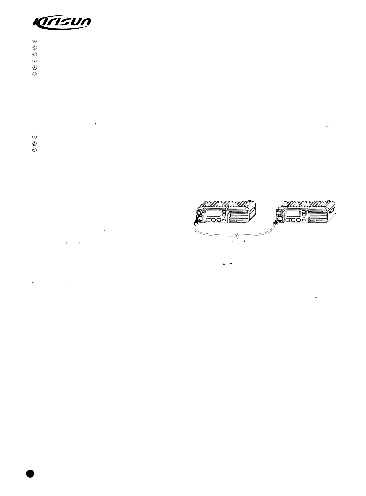
Cable Copy Mode
The vehicle station will not exit automatically after entering cable copy mode
if the cable copy function is set. But the user need to turn on the power again
if return the user mode.
The operation steps are as follows:
Main machine
Cable copy line KCL02
Sub machine
Figure 4-2
1. Press [P1] and connect the power at the same time for entering copy
mode when it C appears. Please enter user mode if copy mode is
prohibited.
2. Connect sub-machine with cable copy line (KCL02) and turn on the power
of sub-machine.
3 .Press [P2] of Host for copy with the red indicator on, thus the data can be
copied from Host to sub-machine. The sub-machine shows P with green
indicator on when receiving the data. The red indicator of Host is off after
copy, while sub-machine reset automatically after receiving all data.
4. You may continue the copy of step 3.
Notes: You may turn on or prohibit cable copy mode by PC Programming
Software. The vehicle station can not enter cable copy mode once the cable
copy function is prohibited.
Chapter 5 Maintenance, Assembly and Disassembly
The station is a kind of sophisticated communication equipment with small
and fine mechanical structure. You should assemble and disassemble it
carefully during the maintenance process. The Instruction for assembly and
disassembly are as follows:
Page 10

1.Exploded view of the station
PT8000 SERVICE MANUAL
Figure 5-1
ITEM
PART NUMBER
1
201-008000-R02
2
203-006800-R26
3
203-007200-R08
4
204-006800-R01
5
6
301-25050J-R01
7
201-008000-R01
8
204-008000-R01
9
121-100000-R19
10
120-400000-R04
11
120-400000-R05
12
204-008000-R02
13
204-008000-R03
14
203-008000-R02
15
120-100000-R15
16
201-008000-R06
17
203-008000-R03
18
202-008200-R02
19
303-30100G-R01
20
203-008200-R03
21
102-304452-R01
22
203-008200-R05
23
203-008200-R09
24
25
301-30060G-R01
DESCRIPTION
KNOB VOLUME
SPRING PLATE
NUT VOLUME KNOB
LABEL LCD LENS
LABEL LOGO
SCREW M2.5*5
CASE FRONT
NET DUSTPROOF SPEAKER
SPEAKER
LINE SPEAKER
LINE 0.5*34P*110mm
STRIP DUSTPROOF C
STRIP DUSTPROOF B
CASE TOP AL
CABLE POWER
FASTENER POWER CABLE
PLATE METAL
PLUG RUBBER SPEAKER HOLE
SCREW M3*10 WITH SPRING PLATE
ANTENNA BASE
MODULE POWER
SHIELD POWER MOUDLE
CUSHION SHIELD
PCB ASSEMBIY MAIN
SCREW M3*6
QTY.
1
1
1
1
1
6
1
1
1
1
1
1
1
1
1
1
1
1
1
1
1
1
8
ITEM
26
27
28
29
30
31
32
33
PART NUMBER
204-008000-R04
203-008000-R01
301-30250D-R01
201-008000-R04
201-008000-R03
202-008000-R01
302-26060D-R01
DESCRIPTION
STRIP DUSTPROOF A
CASE BOTTOM AL
SCREW M3*25
LENS LED
LENS LCD WINDOW
KEY RUBBER
PCB ASSEMBLY CONTROL
SCREW M2.6*6
QTY.
2
1
6
1
1
1
1
5
9
Page 11

PT8000 SERVICE MANUAL
2.Instruction for disassembly of the station for maintenance
1 RF-PCB Disassembly
Release the 6 screws (M3x25) for the upper and lower covers and
open the aluminum alloy lower cover (see the figure below).
2 Instruction for disassembly of KEY-PCB
Figure 5-4
.Release the 6 screws (M3x25) for the upper and low er covers and open
the aluminum alloy lower cover (see the figure above).
.Unplug the flat cable and horn cable.
.Release the 2 screws (M2.5x5) for the panel to separate the pa nel from
the station.
.Unplug the volume knob and then remove the knob circlip and the switch
nub.
.Release the 5 fixing screws (M2.6x6) for KEY-PCB to take out the KEYPCB from the plastic panel (see the figure above).
After the disassembly above, you can carry out corresponding reparation
and debugging according to the actual malfunction.
Chapter 6 Overall Debugging
Please ensure good grounding of all equipment before testing/debugging
Please ensure the correct connection of antenna output with the corresponding equipment or load before testing/debugging.
Figure 5-2
.Remove the power module shield and unsolder the welding leg of
power amplification module from PCB with the electric iron (see the figure
above).
.Release the 4 screws (M2.5x5) of the baffle and remove the metal baffle,
plastic buckle and horn hole plug (see the right figure above).
.Unplug the flat cable and horn cable, unsolder the antenna head from
RF-PCB with the electric iron, release the screws and then carefully remove
the RF-PCB from the aluminum alloy upper cover (see the figure below).
Figure 5-3
Transmitter output must connect with standard signal source/ frequency
meter/ frequency deviator/frequency spectrograph by RF Power Attenuator.
Please ensure no transmitting operation when testing the receiver.
Please ensure the good antistatic measures for human body and equipment during the debugging /testing/reparation process.
6.1 Equipment and software for repair
It is necessary to list the equipment and software in the following table to
repair and test this product.
Table 6.1 For repair and test: equipment and software
Name
N
O.
Computer
1
Programming software
2
Programming cable
3
Dubbing cable
4
DC regulator
5
power meter
6
RF
Frequency
7
meter
Frequency
8
deviator
DMM
9
Audio signal generator
10
Parameter requirements
Above P2, compatible IBM PC, WINDOWS
98/ME/2000/XPOperating System
KSP8000
KSPL-05
KCL-02
Output voltage:13.8V, output electric
current: 20A
Test range: 0.5---50W
Frequency range: 100MHz500MHz
Resistance: 50Ù
SWR 1.2
Frequency range: 0.1600MHz
Frequency accuracy: higher than 1 10
Sensitivity: higher than 100mV
Frequency range: DC600MHz
Test range: 0-- 5kHz
Input resistance: above 10MÙ/V DC,
capable of measuring voltage, electric
current and resistance.
Frequency range:2---3000Hz
Output level: 1---500mV
-6
10
Page 12

PT8000 SERVICE MANUAL
N Name Parameter requirements
O.
power attenuator
RF
11
Standard signal source
12
Oscillograph
13
Audio Frequency voltmeter
14
Recommend how to use: item 6, 7, 8, 10, 11 and 12 which listed in the table
can be substituted by integrated tester Hp8920.
Figure 6.1 External microphone Interface Definition
6.2 Debugging
6.2.1 VCO Adjustment
a.Adjust channel to high frequency point see Table 6.2
b.In the rec eiving state, test voltage of PD by DMM and adjust fine tuning capacitor C122 to get PD voltage of 3.5V 0.1V
c.In the transmitting state, test voltage of PD by DMM and adjust fine tuning capacitor C39 to get PD voltage of 3.5V 0.1V
d.Adjust channel to low frequency point see Table 6.2
e.In the receiving state, test voltage of PD by DMM (>0.6V)
f.In the transmitting state, test voltage of PD by DMM (>0.6V)
Table 6.2High/ Intermediate/ Low Frequency Point of All Models
Low Frequency
PT8000(2) 400.125MHz 425.125MHz 449.975MHz
PT8000(3) 438.125MHz 464.125MHz 489.975MHz
6.2.2 Transmitting frequency offset adjustment (HP8920 is set to TX state
and filter is at 50Hz~ 15kHz) :
a.Input audio signal of 60mV, 1000Hz at MIC jack of vehicle station.
b.Adjust channel to low frequency point see Table 6.2
c.Press PTT to adjust VR2 and set frequency offset to 4.2kHz
d.Observe frequency offset of other channels (>3.5kHz)
6.2.3 PLL frequency calibration (HP8920 is set to TX state)
Enter Frequency Stability in Computer Test Mode to achieve the
rated transmitting frequency by adjusting the number from 0 to 255
(Error<100Hz).
6.2.4 Transmitting frequency adjustment (HP8920 is set to TX state)
a.Enter Transmitting High Power in Computer Test Mode to
adjust the five frequency points including min., low, intermediate, high
and max points respectively and set transmitting power to 22W by
adjusting the number from 0 to 255.
b.Enter Transmitting Low Power in Computer Test Mode to adjust
the five frequency points including min., low, intermediate, high and
Decrement: 40db or 50db
Receive power : higher than 50W
Frequency range:10MHz---1000MHz
Output level:0.1uV~32mV
(-127dBm~-17dBm)
Frequency range: DC~20MHz
Test range: 10mV~20V
Test range: 10mV~10V
PointIntermediate
Frequency Point
High Frequency Point
max points respectively and set transmitting power to 5W by adjusting the
number from 0 to 255.
6.2.5 Smooth regulation for DCS waveform (HP8920 is set to TX state
and filter is at 20Hz~300Hz)
Enter DCS frequency offset in Computer Test Mode to adjust
VR1 close to square wave.
6.2.6 DCS frequency offset (HP8920 is set to TX state and filter is at
20Hz~300Hz)
a.Enter DCS frequency offset in Computer Test Mode and select
Broadband to set the frequency offset to 0.75 kHz by adjusting the
number from 0 to 255 and the five frequency points including min., Low,
intermediate, high and max points.
b.Enter DCS frequency offset in Computer Test Mode and select
Narrowband to set the frequency offset to 0.35 kHz by adjusting the
number from 0 to 255.
6.2.7 (QT67) frequency offset (HP8920 is set to TX state and filter is at
20Hz~300Hz)
a.Enter (QT67) frequency offset in Computer Test Mode and
select Broadband to set the frequency offset to 0.75 kHz by adjusting
the number from 0 to 255 and the five frequency points including min.,
low, intermediate, high and max points.
b.Enter (QT67) frequency offset in Computer Test Mode and
select Narrowband to set the frequency offset to 0.35 kHz by adju sting the number from 0 to 255.
6.2.8 (QT254) frequency offset (HP8920 is set to TX state and filter is at
20Hz~300Hz)
a.Enter (QT254) frequency offset in Computer Test Mode and
select Broadband to set the frequency offset to 0.75 kHz by adju
sting the number from 0 to 255 and the five frequency points including
min., low, intermediate, high and max points.
b.Enter (QT254) frequency offset in Computer Test Mode and
select Narrowband to set the frequency offset to 0.35 kHz by adju sting the number from 0 to 255.
6.2.9 Receiving Sensitivity (HP8920 is set to RX)
Enter Receiving Sensitivity in Computer Test Mode to adjust the
five frequency points including max, high, intermediate, low and min.
points and the number from 0 to 255 for setting max sensitivity of all points.
6.3.0 Receiver Squelch setting (HP8920 is set to RX)
a.Enter SQL9 open in Computer Test Mode (input the frequency
of adjusted frequency point, transmitting signal with amplitude of -115dBm,
audio frequency of 1kHz and frequency offset of 3kHz in antenna interface
of vehicle station) and click Broadband to adjust the five frequency
points including min., low, intermediate, high and max points.
b.Enter SQL9 open in Computer Test Mode (input the frequency
of adjusted frequency point, transmitting signal with amplitude of -115dBm,
audio frequency of 1kHz and frequency offset of 1.5kHz in antenna int erface of vehicle station) and click Narrowband to adjust the five
frequency points including min., low, intermediate, high and max points.
c.Enter SQL9 close in Computer Test Mode (input the frequency
of adjusted frequency point, transmitting signal with amplitude of -116dBm,
audio frequency of 1kHz and frequency offset of 3kHz in antenna inte rface of vehicle station) and click “Broadband” to adjust the five freq uency points including min., low, intermediate, high and max points.
d.Enter SQL9 close in Computer Test Mode (input the frequency
of adjusted frequency point, transmitting signal with amplitude of -116dBm,
audio frequency of 1kHz and frequency offset of 1.5kHz in antenna int erface of vehicle station) and click Narrowband to adjust the five fre quency points including min., low, intermediate, high and max points.
e.Enter SQL1 close in Computer Test Mode (input the frequency
of adjusted frequency point, transmitting signal with amplitude of -122dBm,
audio frequency of 1kHz and frequency offset of 3kHz in antenna inter face of vehicle station) and click Broadband to adjust the five frequ ency points including min., low, intermediate, high and max points.
f.Enter SQL1 open in Computer Test Mode (input the frequency
11
Page 13

of adjusted frequency point, transmitting signal with amplitude of -122dBm,
audio frequency of 1kHz and frequency offset of 1.5kHz in antenna int erface of vehicle station) and click Narrowband to adjust the five fre quency points including min., low, intermediate, high and max points.
g.Enter SQL1 close in Computer Test Mode (input the frequ ency of adjusted frequency point, transmitting signal with amplitude of
-123dBm, audio frequency of 1kHz and frequency offset of 3kHz in an tenna interface of vehicle station) and click Broadband to adjust the
five frequency points including min., low, intermediate, high and max
points.
h.Enter SQL1 close in Computer Test Mode (input the frequ ency of adjusted frequency point, transmitting signal with amplitude of
-123dBm, audio frequency of 1kHz and frequency offset of 1.5kHz in
antenna interface of vehicle station) and click Narrowband to adjust
6.3.2 Adjusting explanation
Please refer Table3, 4 and 5 for the debugging of the parts above
Table 6.3 Voltage controlled oscillator
Item
Setting
Locking
voltage
Test condition
Supply voltage battery terminal:13.8V
CH: Receiving high frequency point
CH: Receiving low frequency point
CH: Transmitting high frequency point
CH: Transmitting low frequency point
Instrumentation
DMM
PT8000 SERVICE MANUAL
the five frequency points including min., low, intermediate, high and max
points.
6.3.1 DTMF frequency offset (HP8920 is set to TX state and filter is at 50Hz
~15 kHz)
a.Enter DTMF frequency offset in Computer Test Mode and select
Narrowband to set frequency offset to 3.5 kHz by adjusting the five
frequency points including min., low, intermediate, high and max points
and the number from 0 to 255.
b.Enter DTMF frequency offset in Computer Test Mode and select
Narrowband to set frequency offset to 1.7 kHz by adjusting the number
from 0 to 255.
Test point
PD
Correcting member
C122
C39
Requirement
3.5V 0.1V
>0.6V
3.5V 0.1V
>0.6V
Remarks
Adjustment
Observation
Adjustment
Observation
Table 6.4 Receiving part
Item
BPF
Audio
Power
Sensitivity
Squelch
Test condition
Test frequency:
Intermediate
Frequency Point
Antenna Interface Input:
RF OUT: -47dBm(1 V)
MOD: 1kHz
DEV: 3.0kHz/ 1.5kHz
Audio load: 16
CH: Low Frequency Point
CH: Intermediate
Frequency Point
CH: High Frequency Point
therefore OUT:
-119dBm(0.25 V)
MOD: 1kHz
DEV: 3.0kHz/ 1.5kHz
CH: Receiving Center
Frequency Point
Level-9
RF OUT output:-114dBm
Level-1
RF OUT output:-121dBm
Instrumentation
Spectrum Analyzer /
Integrated Tester
therefore signal
generator
Oscillograph
Audio frequency
voltmeter
distortion tester
/Integrated tester
Test point
Before
Mixing
Speaker
Interface
Correcting member
Test mode
Test mode
Test mode
Test mode
Requirement
Smooth Wave.
(Volume knob clockwise to the
end) Audio Power>4W
SINAD
12dB or higher
Normal squelch opening
after adjustment
Normal squelch opening
after adjustment
Remarks
User's adjustment
not recommended
12
Page 14

Table 6.5 Transmitting part
Item
RF rate
DCS waveform
(balance)
Power
Max Modulation
Frequency
Deviation
DTMF DEV
CTCSS DEV
CTCSS DEV
DCS DEV
Test condition
CH: Transmitting
Low Frequency Point
AG: 1kHz/60mV
CTCSS: 67Hz
CTCSS: 254.1Hz
DCS: 023N
Instrumentation
Frequency Counter / Integrated Test er
Oscillograph / Integrated Tester
Power Tester / Integrated Tester
Ammeter
Frequency deviator/Integration Test er
Frequency deviator/Integration Test er
Frequency deviator/Integration Test er
Frequency deviator/Integration Test er
Frequency deviator/Integration Test er
Test point
Antenna
PT8000 SERVICE MANUAL
correcting member
Test mode
VR1
Test Mode
VR2
Test Mode
Test Mode
Test Mode
Test Mode
requirement
Within 100Hz
Nearly flat waveform
Square wave
Adjust to 22W/5W
Adjust to 4.2kHz/2.1kHz
Adjust to 3.5kHz1.7 kHz
Adjust to 0.75kHz /0.35 kHz
Adjust to 0.75kHz /0.35 kHz
Adjust to 0.75kHz /0.35 kHz
remarks
200Hz
50Hz
Chapter 7 Main Technical Indexes
7.1 General Indexes
Model
Frequency
Modulation
Number of channels
Channel separation
IF
Working voltage
Working temperature
Antenna Impedance
Microphone Impedance
Dimension
Weight
7.2 Receiving part
Usable Sensitivity (12dB SINAD)
Squelch-on sensitivity
Receiver residue output
Modulation receiving bandwidth
Adjacent channel selectivity
Intermodulation immunity
Spurious response immunity
Audio Output Power
Receiving consumption current
Standby current
7.3 Transmitting part
Transmitting Power
Frequency Stability
Max Modulation Frequency Deviation
Modulation Distortion 300~3000Hz
Adjacent-channel Transmitting Power
Spurious Emissions
Residual FM
Transmitting Consumption Current
PT8000
(1) (136 ~ 174) MHz(2) (400 ~ 450) MHz
(3) (438 ~ 490) MHz(5) (350 ~ 400) MHz
16K F3E/11K F3E
8
25 kHz/12.5kHz
1St IF: 49.95MHz 2nd IF: 450kHz
13.8V Negative Earth
-25 ~ +55
50
2.2k
W -45dB/N -40dB
W 7kHz/N 3.5kHz
W 70dB/N 60dB
4W, Balance @ Distortion 5% 16
-118dBm
-121dBm @ Level-1 Squelch
65dB
70dB
1A
100mA
20W/5W @13.8V DC
2.5ppm
5kHz/ 2.5kHz
3%
W 70dB/N 60dB
70 dB
W -45dB/N -40dB
7A @ 13.8V DC
Chapter 8 Trouble Shooting Guide
Problem
No.
Power on Failure
1
Phase lock loop
2
unlocked (Beeping)
No talkback
3
No receiving signal
4
The red transmission
5
Indicator lights but no
sound is heard.
The green receiving
6
indicator lights but no
sound is heard.
Solution
A. The power cable is not connected with the
accumulator or the host reliably. Please connect the power cable reliably.
B. The protective tube of power cable is burnt
out. Please change it.
C. The power button is of poor contact. Please
change the silica gel button or PCB button.
D. The rechargeable battery is out of power.
Please recharge or change a new one.
E. CPU is broken, Please change the IC.
A. Channel frequency beyond the range, reset
channel data.
B. The crystal X1 of phase lock loop is broken.
Please change it.
C. The oscillator tube is broken. Please change it.
D. The IC3 of phase lock loop is broken. Please
change IC.
A. The frequency is not right. Please reselect
the channel of the same frequency.
B. The CTCSS/DCS code is not the same.
Please reset it.
C. It is out of the effective communication range.
A. The antenna is not in good contact. Please
fasten the antenna head.
B. The high-frequency amplifying tube Q18 is
broken. Please change it.
C. The squelch level is set to high Please reset
the squelch level.
D. The mixed tube Q19 is broken. Please
change it.
E. The FM IC6 is broken. Please change IC.
A. Power module IC1 damaged, no power
output, please change the module.
B. MIC damaged, please change it.
A. The speaker is broken. Please change it.
B. The audio power amplifierIC7 is broken.
Please change IC.
13
Page 15

Appendix 1 Abbreviations
AMP amplify, amplifier
ANT antenna
APC automatic power control
BPF band pass filter
CTCSS continuous tone control squelch system
DCS Digital code squelch
DEMOD demodulation
E2PROM E2PROM
HPF high pass filter
IDC instantaneous deviation control
IF intermediate frequency
LED Light-Emitting Diode
LNA low noise amplifier
LPF low pass filter
Appendix 2 Mainboard Bom(438-490MHz)
PT8000 SERVICE MANUAL
MCU micro control unit
MIC microphone
MOD modulation
MONI monitor
PLL phase lock loop
PTT push-to-talk
RX
SPK speaker
TCXO temperature control X' oscillator
TX
UL un-lock
VCO voltage control oscillator
N
Material Serial No.
O.
1
101-08000U-R03
2
102-0R8C2A-R01
3
102-304452-R01
4
102-9140NR-R01
5
102-A1519C-R01
6
102-A31136-R01
7
102-AT2408-R01
8
102-B15E03-R01
9
102-FP3502-R01
10
102-HT9172-R01
11
102-M2902V-R01
12
102-M2904V-R01
13
102-M78L05-R01
14
102-TA7808-R01
15
103-0DA221-R01
16
103-0MA742-R01
17
103-1SS372-R01
18
103-1SV278-R01
19
103-A2S111-R01
20
103-AP1250-R01
21
103-DAN222-R01
22
103-HSC277-R01
23
103-HVC355-R02
24
103-HVC376-R01
25
103-HZU5AL-R01
26
103-SM3MA1-R01
27
104-A144EE-R01
28
104-C144EE-R01
29
104-MT717T-R01
30
104-SC3357-R01
31
104-SC4116-R01
32
104-SC4617-R01
33
104-SC4919-R01
34
104-SC5108-R01
35
104-TA1298-R01
36
105-2SK508-R01
37
105-3SK318-R01
38
105-SK1824-R01
39
105-SK1829-R01
Name/Spec.
PT8000PCB / PT8000U-080403.PCB,ROHS
MCU / R8C/2A,R5F212A8SNFP ,PLQP-64,ROHS
Power module / RA30H4452M ROHS
MOS IC / PST9140NR,ROHS
MOS IC / TDA1519C,SIL9,ROHS
MOS IC / TA31136FN,SSOP ,ROHS
MOS IC / A T24C08AN-SU27,ROHS
MOS IC / MB15E03SL,PLL,16-PIN,SSOP ,ROHS
MOS IC / XC62FP3502PR,SOT-89,ROHS
MOS IC / HT9172,SOP ,ROHS
MOS IC / NJM2902V,OP-AMP,ROHS
MOS IC / NJM2904V,OP-AMP,ROHS
MOS IC / NJM78L05UA ROHS
MOS IC / TA7808S,TO-220,ROHS
Chip diode / DA221(ROHM),ROHS
Chip diode / MA742(PANASONIC),ROHS
Chip diode / 1SS372(TOSHIBA),ROHS
Chip variable capacitor diode/ 1SV278,ROHS
Chip diode / 0603,MA2S111(PANASONIC),ROHS
Chip diode / MA4P1250-1072T,ROHS
Chip diode / DAN222,(ROHM),ROHS
Chip diode /,HSC277(HITACHI),ROHS
Chip variable capacitor diode/ 0603,HVC355B(HITACHI),ROHS
Chip variable capacitor diode/ HVC376B,ROHS
Chip diode / HZU5ALL(HITACHI),ROHS
Chip diode / DSM3MA1,ROHS
Chip capacitor / DTA144EE(ROHM),ROHS
Chip capacitor / DTC144EE(ROHM),ROHS
Chip capacitor / FMMT717TA,ROHS
Chip capacitor / 2SC3357 ROHS
Chip capacitor / 2SC4116-GR ROHS
Chip capacitor / 2SC4617(S)(ROHM),ROHS
Chip capacitor / 2SC4919,MUTING,CIRCUIT(SANYO),ROHS
Chip capacitor / 2SC5108Y(TOSHIBA),ROHS
Chip capacitor / KTA1298(Y),ROHS
FET / 2SK508NV(K52),ROHS
FET / 3SK318,ROHS
FET / 2SK1824,ROHS
FET / 2SK1829,ROHS
Installation Positon
IC11
IC1
IC12
IC7
IC6
IC15
IC3
IC2
IC5
IC8, IC9, IC13
IC4
IC17
IC16
D13
D9, D10, D25
D32
D8
D12, D15, D22
D3, D11
D20, D21, D33
D2, D19
D23
D1, D4, D5, D6, D14, D16, D17, D18, D26, D27,
D28, D29, D30
D7
D34
Q15, Q23, Q29, Q35, Q36
Q9, Q10, Q17, Q22, Q24, Q25, Q28, Q37, Q42,
Q43, Q44, Q47
Q39
Q4, Q5
Q3, Q13
Q14, Q21, Q26, Q31
Q32
Q1, Q2, Q7, Q11, Q20
Q38, Q40
Q6, Q12
Q18, Q19
Q30, Q33, Q34, Q45, Q46
Q16
14
Page 16

40
108-450C24-R02
41
108-CF450F-R01
42
108-CF450H-R01
43
108-XF4995-R01
44
109-040000-R01
45
109-040100-R01
46
109-040101-R01
47
109-040102-R01
48
109-040103-R01
49
109-040104-R01
50
109-040105-R01
51
109-040122-R01
52
109-040123-R01
53
109-040124-R01
54
109-040151-R01
55
109-040153-R01
56
109-040154-R01
57
109-040183-R01
58
109-040184-R01
59
109-040184-R02
60
109-040204-R01
61
109-040220-R01
62
109-040221-R01
63
109-040223-R01
64
109-040224-R01
65
109-040241-R01
66
109-040272-R01
67
109-040273-R01
68
109-040274-R01
69
109-040331-R01
70
109-040332-R01
71
109-040333-R01
72
109-040334-R01
73
109-040363-R01
74
109-040392-R01
75
109-040393-R01
76
109-040394-R01
77
109-040433-R01
78
109-040471-R01
79
109-040472-R01
80
109-040473-R01
81
109-040474-R01
82
109-040560-R01
83
109-040561-R01
84
109-040562-R01
85
109-040563-R01
86
109-040564-R01
87
109-040682-R01
88
109-040683-R01
89
109-040684-R01
90
109-040821-R01
91
109-040824-R01
450kHz Phase Frequency Detector /
JTBM450CX24,ROHS
Plug-in porcelain filter / LTM450FW,
450kHz 7kHz,ROHS
Plug-in porcelain filter / LTM450HT,
450kHz 3kHz,ROHS
Plug-in IF filter / 49.95MHz 7.5KHz,
U-5*2,ROHS
Chip resistor / 0402,0R 5%,ROHS
Chip resistor / 0402,10R 5%,ROHS
Chip resistor / 0402,100R 5%,ROHS
Chip resistor / 0402,1K 5%,ROHS
Chip resistor / 0402,10K 5%,ROHS
Chip resistor / 0402,100K 5%,ROHS
Chip resistor / 0402,1M 5%,ROHS
Chip resistor / 0402,1.2K 5%,ROHS
Chip resistor / 0402,12K 5%,ROHS
Chip resistor / 0402,120K 5%,ROHS
Chip resistor / 0402,150R 5%,ROHS
Chip resistor / 0402,15K 5%,ROHS
Chip resistor / 0402,150K 5%,ROHS
Chip resistor / 0402,18K 5%,ROHS
Chip resistor / 0402,180K 1%,ROHS
Chip resistor / 0402,180K 5%,ROHS
Chip resistor / 0402,200K 5%,ROHS
Chip resistor / 0402,22R 5%,ROHS
Chip resistor / 0402,220R 5%,ROHS
Chip resistor / 0402,22K 5%,ROHS
Chip resistor / 0402,220K 5%,ROHS
Chip resistor / 0402,240R 5%,ROHS
Chip resistor / 0402,2.7K 5%,ROHS
Chip resistor / 0402,27K 5%,ROHS
Chip resistor / 0402,270K 5%,ROHS
Chip resistor / 0402,330R 5%,ROHS
Chip resistor / 0402,3.3K 5%,ROHS
Chip resistor / 0402,33K 5%,ROHS
Chip resistor / 0402,330K 5%,ROHS
Chip resistor / 0402,36K 5%,ROHS
Chip resistor / 0402,3.9K 5%,ROHS
Chip resistor / 0402,39K 5%,ROHS
Chip resistor / 0402,390K 5%,ROHS
Chip resistor / 0402,43K 5%,ROHS
Chip resistor / 0402,470R 5%,ROHS
Chip resistor / 0402,4.7K 5%,ROHS
Chip resistor / 0402,47K 5%,ROHS
Chip resistor / 0402,470K 5%,ROHS
Chip resistor / 0402,56R 5%,ROHS
Chip resistor / 0402,560R 5%,ROHS
Chip resistor / 0402,5.6K 5%,ROHS
Chip resistor / 0402,56K 5%,ROHS
Chip resistor / 0402,560K 5%,ROHS
Chip resistor / 0402,6.8K 5%,ROHS
Chip resistor / 0402,68K 5%,ROHS
Chip resistor / 0402,680K 5%,ROHS
Chip resistor / 0402,820R 5%,ROHS
Chip resistor / 0402,820K 5%,ROHS
PT8000 SERVICE MANUAL
CD1
Cf2
Cf1
Xf1, XF2
C134, C135, C162, C289, R66, R72, R145, R149, R172, R186, R196, R197,
R222, R223, R229, R238, R242, R252, R257, R268, R282, R287
R2, R3, R71, R82, R84, R219
R21, R26, R101, R121, R247
R9, R48, R70, R78, R83, R136, R188, R194, R201, R206, R231, R235,
R254, R266, R270, R292
R10, R12, R13, R15, R20, R24, R35, R62, R65, R68, R74, R79, R81, R112,
R174, R210, R228, R233, R237, R280, R283, R284, R285
R40, R52, R53, R60, R64, R67, R80, R92, R117, R123, R199, R208, R225,
R236, R239, R248, R269, R273
R128, R130, R131, R132, R133, R137, R139, R147, R192, R277
R152, R267
R88, R245
R150, R175
R63, R111
R49, R50, R56, R155, R162, R272
R6, R11, R27, R140, R216
R198, R207, R217, R259
R169, R170, R221
R93, R143
R69
R33, R37, R103
R115
R85, R86, R106, R109, R110, R153, R171, R215
R183, R213
R61
R1, R57, R148
R59, R161, R177, R205
R42, R141, R164
R14, R43
R124, R142, R146, R159, R173
R151, R156, R157, R185, R249
R73, R108, R134, R230
R98
R271, R279
R278
R202, R220
R160, R163
R100
R5, R16, R39, R76, R77, R91, R179, R187, R191, R195, R288, R289, R290
R75, R89, R105, R126, R127, R129, R293, R294
R96, R165, R204
R135
R51, R54, R55
R178, R184, R193, R212, R241, R260
R97, R125, R232, R258, R263, R275
R99, R243
R94, R95, R113, R114, R244
R118, R264, R274
R209
R255
R224
15
Page 17

109-040913-R01
92
109-060000-R01
93
109-060100-R01
94
109-060102-R01
95
109-060121-R01
96
109-060151-R01
97
109-060221-R01
98
109-060271-R01
99
109-060272-R01
100
109-060274-R01
101
109-060471-R01
102
109-0605R6-R01
103
109-060681-R01
104
109-060821-R01
105
109-070000-R01
106
109-070220-001
107
109-070470-001
108
109-100221-R01
109
110-110473-R01
110
110-110683-R01
111
111-010000-R01
112
111-030000-R01
113
112-043100-R01
114
112-043101-R01
115
112-043102-R01
116
112-043103-R01
117
112-043104-002
118
112-043104-R02
119
112-043105-R01
120
112-043110-R01
121
112-043120-R01
122
112-043123-R01
123
112-043150-R01
124
112-043180-R01
125
112-043182-R01
126
112-0431R0-R01
127
112-0431R5-R01
128
112-043220-R01
129
112-043221-R01
130
112-043222-R01
131
112-043223-R01
132
112-0432R0-R01
133
112-0432R5-R01
134
112-043330-R01
135
112-043331-R01
136
112-043333-R01
137
112-043390-R01
138
112-043392-R01
139
112-043393-R01
140
112-0433R0-R01
141
112-043470-R01
142
Chip resistor / 0402,91K 5%,ROHS
Chip resistor / 0603,0R 5%,ROHS
Chip resistor / 0603,10R 5%,ROHS
Chip resistor / 0603,1K 5%,ROHS
Chip resistor / 0603,120R 5%,ROHS
Chip resistor / 0603,150R 5%,ROHS
Chip resistor / 0603,220R 5%,ROHS
Chip resistor / 0603,270R 5%,ROHS
Chip resistor / 0603,2.7K 5%,ROHS
Chip resistor / 0603,270K 5%,ROHS
Chip resistor / 0603,470R 5%,ROHS
Chip resistor / 0603,5.6R 5%,ROHS
Chip resistor / 0603,680R 5%,ROHS
Chip resistor / 0603,820R 5%,ROHS
Chip resistor / 0805,0R 5%,ROHS
Chip resistor / 0805,22R 5%
Chip resistor / 0805,47R 5%,
Chip resistor / 1206,220R 5%,ROHS
Chip trimming resistor / MVR22HXBRN473,
47K 25%,B Linear,ROHS
Chip trimming resistor / MVR22HXBRN683,
68K 25%,B Linear,ROHS
Plug-in voltage-dependent resistor / 10D220 ROHS
Chip Fuse / 433003,3A/32V,1206(429003) ROHS
Chip capacitor / 0402,10P 0.5P ,50V,C0G,ROHS
Chip capacitor / 0402,100P 5%,50V,C0G,ROHS
Chip capacitor / 0402,1000P 10%,50V,X7R,ROHS
Chip capacitor / 0402,0.01uF 10%,50V,X7R,ROHS
Chip capacitor / 0402,0.1uF 10%,10V,X5R,
Chip capacitor / 0402,0.1uF 10%,10V,X5R,ROHS
Chip capacitor / 0402,1uF 10%,6.3V,X5R,ROHS
Chip capacitor / 0402,11P 5%,50V,C0G,ROHS
Chip capacitor / 0402,12P 5%,50V,C0G,ROHS
Chip capacitor / 0402,0.012uF 10%,50V,X7R,ROHS
Chip capacitor / 0402,15P 5%,50V,C0G,ROHS
Chip capacitor / 0402,18P 5%,50V,C0G,ROHS
Chip capacitor / 0402,1800P 10%,50V,X7R,ROHS
Chip capacitor / 0402,1P 0.25P ,50V,C0G,ROHS
Chip capacitor / 0402,1.5P 0.25P ,50V,C0G,ROHS
Chip capacitor / 0402,22P 5%,50V,C0G,ROHS
Chip capacitor / 0402,220P 5%,50V,C0G,ROHS
Chip capacitor / 0402,2200P 10%,50V,X7R,ROHS
Chip capacitor / 0402,0.022uF 10%,50V,X7R,ROHS
Chip capacitor / 0402,2P 0.25P ,50V,C0G,ROHS
Chip capacitor / 0402,2.4P/2.5P 0.1P,50V,C0G,ROHS
Chip capacitor / 0402,33P 5%,50V,C0G,ROHS
Chip capacitor / 0402,330P 10%,50V,X7R,ROHS
Chip capacitor / 0402,0.033uF 10%,16V,X7R,ROHS
Chip capacitor / 0402,39P 5%,50V,C0G,ROHS
Chip capacitor / 0402,3900P 10%,50V,X7R,ROHS
Chip capacitor / 0402,0.039uF 10%,50V,X7R,ROHS
Chip capacitor / 0402,3P 0.25P ,50V,C0G,ROHS
Chip capacitor / 0402,47P 5%,50V,C0G,ROHS
PT8000 SERVICE MANUAL
R190
L52, L62
R29, R30
R18, R19
R41
R4
R45
R44
R34
R36
R32
R8
R58
R22, R23
L29
L30
L31
R46, R47
VR2
Vr1
R281
F1
C7, C53, C80, C138, C139, C307
C36, C37, C81, C90, C91, C99, C103, C105, C108, C112,
C114, C115, C349, C350, C351, C352, C353, C354, C356,
C359, C360, C361, C362, C363
C58, C167, C170, C171, C188, C189, C195, C196, C206,
C212, C214, C221, C231, C266, C311, C321, C370
C33, C102, C121, C133, C145, C153, C191, C242, C256,
C284, C297, C330, C333
C173
C17, C83, C144, C172, C183, C184, C186, C187, C210,
C211, C213, C235, C253, C259, C261, C268, C270, C271,
C295, C300, C308, C319, C325, C329, C334, C337, C338
C56, C120, C267, C278, C280, C291, C298, C303, C304,
C312, C323, C335, C336
C197
C2, C16, C106, C118, C194
C249, C252, C258, C263, C273
C13, C190, C198
C204
C217
C69, C70, C175
C203
C27, C28, C82, C97, C98, C168, C272, C281
C282
C248, C262
C158, C238, C239, C322
C60, C161, C177
C200
C6, C130, C147, C232
C140
C125, C154, C156, C257, C276
C225, C229
C301, C314
C288
C35, C124, C275
C129, C255
16
Page 18

143
112-043471-R01
144
112-043473-R01
145
112-0434R0-R01
146
112-0435R0-R01
147
112-043681-R01
148
112-043683-R01
149
112-043683-R02
150
112-043820-R01
151
112-043821-R01
152
112-0438R0-R01
153
112-0439R0-R01
154
112-043R50-R01
155
112-063102-R01
156
112-063104-R01
157
112-0631R0-R01
158
112-0632R0-R01
159
112-063333-R01
160
112-063471-R01
161
112-0634R0-R01
162
112-0635R0-R01
163
112-0636R0-R01
164
112-063R50-R01
165
112-072105-R01
166
112-072106-R01
167
112-072225-R01
168
112-072475-R01
169
112-073334-R01
170
112-102104-R01
171
112-102105-R01
172
112-102156-R01
173
112-103102-R01
174
112-103106-R01
175
112-103120-R01
176
112-103140-R01
177
112-1031R0-R01
178
112-1032R0-R01
179
112-1034R0-R01
180
112-191477-R01
181
112-201476-R02
182
113-010100-R01
183
114-06E180-R01
184
114-06E560-R01
185
114-06E680-R01
186
114-06G102-R01
187
114-06G120-R01
188
114-06G180-R01
189
114-06G181-R01
190
114-06G220-R01
191
114-06G221-R02
192
114-06G332-R01
Chip capacitor / 0402,470P 10%,50V,X7R,ROHS
Chip capacitor / 0402,0.047uF 10%,16V,X7R,ROHS
Chip capacitor / 0402,4P 0.25P ,50V,C0G,ROHS
Chip capacitor / 0402,5P 0.25P ,50V,C0G,ROHS
Chip capacitor / 0402,680P 10%,16V,X7R,ROHS
Chip capacitor / 0402,0.068uF 10%,16V,X7R,ROHS
Chip capacitor / 0402,0.068uF 10%,10V,X7R,ROHS
Chip capacitor / 0402,82P 5%,50V,C0G,ROHS
Chip capacitor / 0402,820P 10%,16V,X7R,ROHS
Chip capacitor / 0402,8P 0.5P ,50V,C0G,ROHS
Chip capacitor / 0402,9P 0.5P ,50V,C0G,ROHS
Chip capacitor / 0402,0.5P 0.1P ,50V,C0G,ROHS
Chip capacitor / 0603,1000P 10%,50V,X7R,ROHS
Chip capacitor / 0603,0.1uF 10%,50V,X7R,ROHS
Chip capacitor / 0603,1P 0.25P ,50V,C0G,ROHS
Chip capacitor / 0603,2P 0.25P ,50V,C0G,ROHS
Chip capacitor / 0603,0.033uF 10%,16V,X7R,ROHS
Chip capacitor / 0603,470P 10%,50V,X7R,ROHS
Chip capacitor / 0603,4P 0.25P ,50V,C0G,ROHS
Chip capacitor / 0603,5P 0.25P ,50V,C0G,ROHS
Chip capacitor / 0603,6P 0.5P ,50V,C0G,ROHS
Chip capacitor / 0603,0.5P 0.1P ,50V,C0G,ROHS
Chip T a capacitor ,SIZE P,1uF 20%,10V,ROHS
Chip T a capacitor ,SIZE P,10uF 20%,6.3V,ROHS
Chip T a capacitor ,SIZE P,2.2uF 20%,10V,ROHS
Chip T a capacitor ,SIZE P,4.7uF 20%,10V,ROHS
Chip capacitor / 0805,0.33uF+80%--20%,10V,Y5V,ROHS
Chip T a capacitor ,SIZE A,0.1uF 20%,35V,ROHS
Chip T a capacitor ,SIZE A,1uF 20%,16V,ROHS
Chip T a capacitor ,SIZE A,15uF 20%,6.3V,ROHS
Chip capacitor / 1206,1000P 10%,50V,X7R,ROHS
Chip capacitor / 1206,10uF+80%--20%,16V,Y5V,ROHS
Chip capacitor / 1206,12P 5%,50V,C0G,ROHS
Chip capacitor / 1206,14P 5%,50V,C0G,ROHS
Chip capacitor / 1206,1P 0.25P ,50V,C0G,ROHS
Chip capacitor / 1206,2P 0.25P ,50V,C0G,ROHS
Chip capacitor / 1206,4P 5%,50V,C0G,ROHS
Plug-in electrolytic capacitor / 10*16,470UF25V, 20% ROHS
Chip electrolytic capacitor / 6.3*5.3,47U25V, 20%,ROHS
Chip trimming capacitor / TZV2Z100A110,3~10p+100,ROHS
Chip inductor / C1608CB-18NJ, 18NH 5%,0603,ROHS
Chip inductor / C1608CB-56NJ, 56nH 5%,0603,ROHS
Chip inductor / C1608CB-68NJ, 68nH 5%,0603,ROHS
Chip inductor / MLF1608A1R0K,1uH 5%,0603,ROHS
Chip inductor / MLG1608B12NJT,12nH 5%,0603,ROHS
Chip inductor / MLG1608B18NJT,18nH 5%,0603,ROHS
Chip inductor/ LGHK1608R18J-T,180nH 5%,0603,ROHS
Chip inductor / MLG1608B22NJT,22nH 5%,0603,ROHS
Chip inductor/ LGHK1608R22J-T,220nH 5%,0603,ROHS
Chip inductor / MLF1608A3R3K,3.3uH 5%,0603,ROHS
PT8000 SERVICE MANUAL
C3, C9, C11, C12, C19, C20, C21, C38, C47,
C49, C50, C51, C52, C54, C55, C57, C59, C68,
C71, C87, C88, C89, C92, C95, C110, C116,
C119, C123, C128, C136, C142, C143, C148,
C151, C157, C160, C169, C174, C178, C185,
C207, C215, C218, C220, C222, C223, C247,
C274, C279, C283, C285, C293, C296, C305,
C309, C310, C315, C317, C326, C328, C332,
C339, C340, C342, C343, C348, C369
C245, C294, C306
C100, C107, C126
C72, C73, C166, C205
C132
C155, C244, C320
C357, C358
C234
C324
C192
C93
C48, C62, C65
C26
C96
C4, C5, C176
C40
C18
C22, C23, C24, C25, C64, C67, C77, C78,
C79, C84, C85, C86, C101, R7
C30, C32, D24
C10, C34
C31
C41, C111
C290
C327
C233, C237, C313
C1, C8, C42, C131, C159, C216, C226, C246,
C286, C345, C346
C181
C109, C113
C117
C137, C149
C29
C265
C45
C94
C43
C15
C61
C331
C66, C74, C341, C344
C39, C122
L20, L45
L36
L47, L53
L48
L14, L15
L13
L2
L7, L8
L12, L21, L27, L44
L5, L37
17
Page 19

PT8000 SERVICE MANUAL
193
114-06G471-R01
194
114-06G561-R01
195
114-06G820-R01
196
114-08E103-R01
197
114-08E331-R01
198
114-08E821-R01
199
114-10D170-R01
200
114-10D330-R01
201
115-1R23R0-R01
202
115-2R02R0-R01
203
115-3R0110-R01
204
115-3R06R0-R02
205
117-000000-R05
206
117-000000-R07
207
117-000000-R08
208
119-060104-R01
209
122-116M80-R02
210
122-13M580-R01
211
122-17M300-R01
212
124-020000-R08
213
124-050000-R14
214
124-090000-R01
Chip inductor / MLF1608DR47K,470nH 10%,0603,ROHS
Chip inductor / MLF1608DR56K,560nH 10%,0603,ROHS
Chip inductor / MLG1608B82N,82nH 5%,0603,ROHS
Chip inductor / FSLM2520-100J,10uH 5%,1008,ROHS
Chip inductor / FSLM2520-R33K,330nH 10%,1008,ROHS
Chip inductor / FSLM2520-R82K,820nH 10%,1008,ROHS
Chip inductor/ LQW31HN17NJ03L,17nH,1206,MURATA,ROHS
Chip inductor/ LQW31HN33NJ03L,33nH,1206,MURATA,ROHS
Chip air-cored coil / 0.4*1.2*3TR,ROHS
Chip air-cored coil / 1.4*2.0*2TR,ROHS
Chip air-cored coil / 0.9*3.0*11TR,ROHS
Chip air-cored coil / 0.9*3.0*6TR,ROHS
Chip bead / EMI,FILTER, SMT,BLM21P300S,0805,ROHS
Chip bead / EMI,FILTER, SMT,BLM41P600SPT,1206,ROHS
Chip bead / EMI,FILTER, SMT,BLM11A601S,0603,ROHS
Temperature Chip resistor / NTH5G16P42B104K07TH,100K,0603,ROHS
Chip crystal resonator / TVCGDCSANF,16.8MHz 2.5PPm ROHS
Chip crystal resonator / ZTACC3.58MG,ROHS
Chip crystal resonator / CSTCR7M30G53-R0,7.3M,ROHS
FFC/FPC Connector / 08 6210 034 340 800,34PIN,P=0.5mm,ROHS
3.5mm Plug-in Speaker-Mic socket / MOTOROLA ,ROHS
2PIN Plug-in Speaker socket / WCPW20-02,ROHS
L41
L42
L34, L38
L40
L49
L50
L3
L35
L51, L54, L55, L56, L57, L58
L9, L10, L11, L28
L19
L18
L64, L72, L73
L25, L26
L1, L4, L23, L24, L32, L33, L39, L59, L60,
L61, L65, L66, L67, L68, L69, L70, L74,
L75, L76, L77
R90, R138
X1
X2
X3
CN4
J1
Cn2
Appendix 3 Structured Part List
Number P/N NAME QTY.
1
2
3
4
5
6
7
8
9
10
11
12
13
14
15
16
17
18
19
20
21
22
23
24
25
26
27
28
29
30
31
120-100000-R38B
120-400000-R04
120-400000-R05
121-100000-R19
201-008000-R01A
201-008000-R02A
201-008000-R03A
201-008000-R04A
201-008000-R05A
201-008000-R06A
202-008000-R01B
202-008200-R02A
203-006800-R26
203-007200-R08
203-008000-R01A
203-008000-R02A
203-008000-R03A
203-008000-R05A
203-008200-R03A
203-008200-R05A
204-006800-R01
204-008000-R01A
204-008000-R02A
204-008000-R03A
204-008000-R04A
204-008200-R09A
301-25050J-R01
301-30060G-R01
301-30250D-R01
302-26060D-R01
303-30100G-R01
cable power
wire speaker
cable 34pin
speaker
case front
knob volume
lens display
lens led
bracket display
SR power cable
key rubber
plug speaker hole
spring plate volume knob
nut volume knob
case top Al
case bottom Al
plate metal of cable power
metal dome rubble key
base antenna
shield cover power module
lable display lens
dustproof net speaker
dustproof up case front
dustproof down case front
dustproof case top and bottom
plate grounding with power module
screw m2.5*5
screw m3*6
screw m3*25
screw m2.6*6
screw m3*10
1
1
1
1
1
1
1
1
1
1
1
1
1
1
1
1
1
1
1
1
1
1
1
1
2
1
6
7
6
5
7
18
Page 20

Appendix 4 Appendix
PT8000 SERVICE MANUAL
Name
Bracket
Powercable
Hand Microphone MIC
Microphone Hanger
Combination Screw
Self-tapping Screw
Type
KME215
Specification
M4.0*10.0
M5.0*16.0
Accessories
Self-tapping Screw
M4.0*16.0
19
Page 21

Appendix 5 PT8000 SPARE MECHANICAL PART BOM
PT8000 SERVICE MANUAL
PART NUMBER
ITEM
604-080000-R02
1
203-007200-R08
2
301-25050J-R01
3
604-080000-R01
4
120-400000-R14
5
202-008000-R01B
6
604-080000-R05
7
120-400000-R15
8
301-26060D-R01
9
604-080000-R03
10
201-008000-R06A
11
203-008000-R03A
12
PT8000 SUBASSEMBLY CASE FRONT 604-080000-R01 BOM
ITEM
PART NUMBER
1
201-008000-R01A
2
204-008000-R01A
3
121-100000-R21
4
201-008000-R04A
PT8000 SUBASSEMBLY VOLUME KNOB (604-080000-R02 BOM
ITEM PART NUMBER DESCRIPTION QTY
1 201-008000-R02A KNOB VOLUME 1
2 203-006800-R26 SPRING PLATE 1
DESCRIPTION
SUBASSEMBLY VOLUME KNOB
NUT VOLUME KNOB
SCREW M2.5*5
SUBASSEMBLY FRONT CASE
LINE SPEAKER
KEY RUBBER
SUBASSEMBLY PCB CONTROL
CABLE 0.5*34P*110mm
SCREW M2.6*6
SUBASSEMBLY CASE TOP AL
FASTENER POWER CABLE
METAL PLATE
DESCRIPTION
CASE FRONT
NET DUSTPROOF SPEAKER
SPEAKER
LENS LED
QTY
1
1
6
1
1
1
1
1
5
1
1
1
QTY
1
1
1
1
PART NUMBER
ITEM
202-008200-R02A
13
120-100000-R15
14
301-30100G-R01
15
203-008200-R03
16
102-304452-R01
17
203-008200-R05A
18
204-008200-R10A
19
20
301-30060G-R01
21
604-080000-R04
22
301-30250D-R01
23
ITEM
PART NUMBER
5
201-008000-R03A
6
204-006800-R01
7
PT8000 SUBASSEMBLY CASE TOP AL 604-080000-R03 BOM
ITEM PART NUMBER DESCRIPTION QTY
1 203-008000-R02A CASE TOP AL 1
2 204-008000-R03A STRIP DUSTPROOF B 1
3 204-008000-R02A STRIP DUSTPROOF C 1
DESCRIPTION
PLUG SPEAKER HOLE
CABLE POWER
SCREW M3*10 WITH SPRING PLATE
ANTENNA BASE
POWER MODULE
SHIELD POWER MOUDLE
CUSHION ELECTRIC
PCB MAIN ELEC. PARTS
SCREW M3*6
SUBASSEMBLY CASE BOTTOM AL
SCREW M3*25
DESCRIPTION
LENS WINDOW
LABLE LCD
LABLE LOGO
QTY
1
1
1
QTY
1
1
7
1
1
1
1
1
8
1
6
PT8000 SUBASSEMBLY CASE BOTTOM AL 604-080000-R04 BOM
ITEM PART NUMBER DESCRIPTION QTY
1 203-008000-R01A CASE BOTTOM AL 1
2 204-008000-R04A STRIP DUSTPROOF A 2
20
PT8000 SUBASSEMBLY PCB CONTROL 604-080000-R05 BOM
ITEM PART NUMBER DESCRIPTION QTY
1 PCB CONTROL ELEC. PART 1
2 203-008000-R05A METAL DOME 1
Page 22

Figure 1 PT8000 Schematic Circuit Diagram
SPEAKER
6
J1 SPK
13.8V
BATTARY
MIC
6
TO ANT
LPF
5
ANT SW
APC
IC4
APC CONTROL
BPF
8T
IC7
TDA1519C
VR1
AF POWER AMP
10K
Number RevisionSize
A3
Title
Date: 2009-1-9 Sheet of
File: X:\PT8000\..\PT800 0 B LOCK DEAGRAM .SchDocDrawn By:
8R
HP
Q26
CTCSS/DCS
SW
Q33
MUTE
IC16
2T
D0D1D2D3DV
TA7808S
IC17
NJM78L05UA
5
BPF
IC5
IC1
RA30H
8R
Q19
MIX
4
8T
Q5
PRE
DRIVE
8T
Q4
RF AMP
TX/RX SW
8T 8R
3
5V
RF AMP
XF1
49.95MHz
Q20
IF AMP
CD1
450KHZ
DET COLL
5V
IC6
IF DEMODULATOR
IC8A IC8BIC8CIC8D
AMP LP LP AM P
8R
CF2
CF1
450KHz
450KHz
AF OUT
AMP
IC10BIC10A
DTMF
DECODER
HP
SW
Q38
IC9C IC9BIC9AIC9D
AMP HP LP LP
LP LP IDC AMP
IC13D IC13AIC13BIC13C
5T
MOD
SW
Q40
8TC
8RC
8R
5V
4
3
Q1 Q2
BUFF
5V
Q21
AMP
NOISE
MOD
D25
DET
RX
TX
Q6
Q14
VCO
2
Q7
BUFF
1
VCO
Q14
RIPPLE
FILTER
5V
LOOP FILTER
5V
3.5V
IC3
UL
A A
PLL IC
MB15E03SL
CKDTUL
*3 2ND LOCAL AMP
X1
TCXO
16.8MHz
QT TCXO
BUSY
8R
Q11
INT
D0
BUSY
SDA
PTT
B B
C C
PF1
PF2
POWER
PF3
PF4
KEY BOARD
X3
7.3MHz
IC15
AT24C08
IC11
CPU
R5F212A8
EEPROM
2
5V
TITEMP
RESET
UL
APC
LE
DTCKPA
E-ALA
MODE
D1D2D3
DV
HOOK
IGN
KEY1 RSSI
2TIN
RXD
TGSW
M-MU
AFCO
A-MU
MD
KEY2
RPTT
SHIFT
TO1
DEV1
DEV2
SCANL
LOWL
RXL
TXL
VCCN
2TOUT SCL
TXD
BLC
MAX
8TC
8RC
SBC
RX
W/N
DATA
CLK
D D
1
21
Page 23

Figure 2 PT8000 Main Board Schematic Circuit Diagram
J1 SPK
C269
INV
9
M/SS
8
VP
7
OUT2
6
GND2
5
OUT1
4
RR
3
GND1
2
NINV
1
C251*C254
*
R168
*
R167
*
IC10 *
C250
*
*
C253 104
R172 0R
R175
120K
C247
471
10K
R174
470K
7
270K
Aout
IC9 NJM2902V
14
C249
153
R173
4.7K
C256
C245
683
C248 222
D31 *
C252
123
14
R169 180K
Dout
Aout1A-in2A+in3V+4B+in5B-in6Bout
IC8 NJM2902V
22K
R171
R170 180K
C244
683
C255
C246
4.7uF/10V
RSSI
APC
DEV2
SHIFT
RESET
HOOK
32
MR
MR
33
HOOK
DATA
34
CLK
CLK
35
INT
INT
36
TXD
TXD
37
RXD
RXD
38
BLC
BLC
39
8TC
8TC
40
8RC
8RC
41
APC
APC
42
SBC
SBC
43
TGSW
44
PA
PA
45
A-MU
46
M-MU
47
AFCO
AFCO
48
495051525354555657585960616263
TI
R105 47K
C265
*
C260
C259
105
C264
*
R181 *
7
8
V+
Aout1A-in2A+in3GND
Q26
2SC4617
C257
333
C258
153
C263 153
5
6
A-in
A+in
R178 5.6K
R184
5.6K
392
C262 472
C261
104
12
13
D-in
D+in
R183
220K
*
47P
L75
R185 33K
RX
MD
2TIN
RX
MD
2TIN
DATA
TGSW
AF-MUTE
MIC-MUTE
TEMP
BUSY
RSSITINC
BUSY
RSSI
TEMP
*
R194 22K
C268
104
10uF
C271
R196 4.7K
C270
6
Bout
R197
R190
91K
5.6K
R193
C273
4
V+
C267
474
R192
1M
R199
C266 102
11
GND
R198
L63
*
Q27
C272
DV
D3
DV
IC11
KEY1
KEY2
KEY2
KEY1
PTT
27P
L36
56nH
4P
C93
L19
11T
C63
L29
*
D11
L709CE
*
C44
D36
L709CE
C61 10P
C91
101
D9 MA742
C60
2P
C62 0.5P
C43
*
L28
D10
MA742
C48
0.5P
C65
0.5P
C90
101
R47 220R
L18
6T
R46 220R
*
C46
C8222PC81101
C45
6P
L26
C55 471
C66
47uF/25V
BLM41P600SPT
L25
471
C92471
C51
D7 H ZU5ALL
C74
R23 430R
R43
47uF/25V
C372
*
L24
BLM11A601S
R22 430R
2P
C64
471
C79
471
L31
L15
18nH
100R
1K
R19
R30
10R
D13
R34 2.7K
C78 471
C86 471
C75
*
R41
120R
471
C67
L30
L14
18nH
C85 471
100R
1K
R18
R29
10R
470R
C77 471
C84 471
R32
R45 220R
L22
*
R38
*
C76
*
R28
*
*
R17
*
Q8
R25 180R
*
R31
180R
L17
*
L16
4.7K
C54
471
R16
C50
471
C49
471
330R
R14
R33
22R
10K
R13
C89
471
R21
100R
C59
471
C57
471
392
R20
10K
C68
471
R44 270RL27 220nH
C83
104
R26 100R
2SK508NV(K52)
Q6
C71
471
C87
471
L21 220nH
C39 10P
C70
1P
R36
270K
R42
270K
C69
1P
D8
R39
4.7K
1SV278
C41 0.5P
D6 HVC376B
L23
BLM11A601S
TX OR RX H:4.0V
C80 10P
R27
150K
C88
471
2SC5108
Q7
18nH
C53
10P
R37
22R
C73 5P
L20
18nH
C72 5P
C52
471
C42 4.7uF/10V
C58
102
8
5
7
6
4
DO
FIN
VCC
GND
XFIN
CLOCK9DATA10LE11PS12ZC13LD/FOUT14P/15R/
R40
100K
R48
MA2S111
D12
R15 10K
R24 10K
R35 10K
CK
C100
33P
*
R72
0R
C152
R53
22K
2T
R52
22K
C94
15P
C98
C99
C97 22P
330R
C102103
Q9
C101
471
L32
BLM11A601S
C95
471
C96
104
L33
BLM11A601S
R51
560R
R55
R54 560R
3
VP
1K
R49
15K
R50 15K
R56
0R
C104
5
6
8
7
V+
B-in
Bout
B+in
R60 100K
R64
100K
*
D15 MA2S111
R59 27K
C119
471
22P
C115
101
C110
471
101
C121
103
R63
150R
DTC144EE
DA221
R58 680R
R62 10K
R65
C111 0.5P
R61 240R
L37 3.3uH
C107
4P
L35
39nH
C118
12P
C106
15P
D14
HVC376B
L34
82nH
C109
0.1uF/35V
C117
1uF/16V
R57
2.7K
560R
C113
0.1uF/35V
C116
471
R66
2
1
OSCIN
OSCOUT
IC3
MB15E03SL
16
C108
101
C103
101
C112
101
C105
101
C114 101
15K
R80 10K
Aout1A-in2A+in3GND
IC4 NJM2904
4
C136
471
R67
100K
R73
330K
R87
*
R81 10K
C157
471
C373
47uF/25V
C230
392
Q10
C128
R68
10K
Q13 2SC4116
C123
471
4P
C126
3P
C124
Q12 2SK508NV(K52)
C122
10P
L38 82nH
C127
D16
HVC376B
D18
HVC376B
D17
C125 333
C130
Q11
R69
C129
0R
16.8MHz
L39
BLM11A601S
R90
100K
T
R75
47K
R83
1K
R79
10K
R89
47K
C160
TX:L TX OFF:H
L46
*
C162
L45
18nH
C161
D19HSC277
L78
BLM11A601S
DTC144EE
471
C137
15uF/6.3V
10K
C153
103
C151
471
10K
Q14 2SC4617
R74
C149
15uF/6.3V
C148
471
*
HVC376B
16.8*3 MHz TX:H RX:L
C141
*
C135 0R
33P
L44
220nH
C147 33P
C1340RL43
*
C146 *
C140
331
L41
470nH
C133 103
471
L42
C142
R82 10R
560nH
2SC5108
200K
C150
*
47P
C139
10P
R70
1K
R86
12K
L40
10uH
393
C156
C138
10P
R85
0R
*
C155
X1
16.8MHz
R84
0R
GND
OUT
2
3
C159
4.7uF/10V
VC
VCC
1
4
R88
C131
4.7uF/10V
R71
C132
15K
C145
103
R78 1KR77820R
C154
182
C144
104
10R
C143
471
C158 182
R76
820R
681
Q16
471
2SK1829
TEMP
TGSW
R93
180K
RSSI
L47
68nH
C166
5P
*
C167
102
C164
0R
6P
C163
R92
100K
2P
*
C165
R91
4.7K
2LO
R94 6.8K R9 5 6.8K
W:H N:L
W:L N:H
RX
Q15
DTA144EE
W:H N:L
Q36
DTA144EE
R280
10K
W/N
BUSY
L76 BLM11A601S
2LO
VCCN
CN1
TO ANT
6
L11
2T
L9
2T
C14 2P C15 4P
C29
102
D3
L709CE
L10
2T
POUT
VDD
C28 22P
C37 101
101
VGG
C27 22P
C36
PIN
5
R8
12R
IC1 RA30H4047M
4
3
2
1
C40
C26 102
*
L6
C31 6P
Q5
2SC3357
C30 6P
Q4
2SC3357
C25
471
471
C23 471 C24
R7 33R
C22 471
C19
471
D2
HSC277
4.7K
R5
C7 10P
L7
22nH
R1
2.7K
Q2
2SC5108
C13 15P
C6
33P
L8
22nH
R6
150K
Q1
2SC5108
C364
392
C371
R1210K
C5 1P
Q3 2SC4116
C4 1P
R4 150R
C47
471
L5 3.3uH
C34 5P
C10 5P
4P
C32
L3
23nH
C16
12P
L12 220nH
C2
12P
D1
D4
HVC376B
HVC376B
HVC376B
D5
L2
180nH
C18
333
R9
1K
C38 471
L13
C35 3P
C33 103
C17 104
C3 471
R3
10R
L1 BLM11 A601S
C8 4.7uF/10V
C20
471
R2 10R
C12
471
L4
C11
471
BLM11A601S
R11 150K
C1 4.7uF/10V
3.5V
OUTIN
IC2
XC62FP3502PR
C9 471
UNLOCK:0V
R10 10K
ULLEDT
C199 *
C168
L57 3T
L54 3T
C201 *
D27
HVC376B
C205 10P
C177
2P
*
R137 1M
R122
4P
D24
L58 3T
C208 *
10P
R133 1M
HVC376B
C194
D28
C174
471
L52
0R
C223
R118
68K
R123 100K
Q18
3SK318
R115
220R
R103
22R
C196
102
R104
*
68nH
C195
102
C214
102
L53
L61BLM11A601S
C200 1P
C169
471
L51
3T
D26
HVC376B
C204 18P
R132
1M
C176
0.5P
R128 1M
C203 1P
C21
D23
HVC355B
15P
R131
1M
3T
L56
R98
36K
R96
470K
D22
R97
56K
R101
XF2
XF1
R100
R99
L48 1uH
D21
CF1
450KHz HT
D20
C56
105
Q17
DTC144EE
DTC144EE
Q37
HVC376B
C198
D30
C202 *
C175
1P
8P
MA2S111
R130
3T
1M
L55
HVC376B
C197
D29
R117
100K
471
C178
R125
56K
C186
104
Q19
3SK318
C207
471
150R
R111
C193
*
L49
C1928PR107
*
0.82uH
L50
0.82uH
L59
BLM11A601S
C191
103
471
C185
C171
102
C218
471
C180
*
100R
49.95MHz
C190
15P
49.95MHz
470R
C179
*
C170
102
560K
Q20
2SC5108
R121 100R
R102
C209
*
*
C182
*
104
C173
DAN222
C217
R120
*
R114 6.8K
CF2 450KHz F
*
R119
6.8K
R113
C221 102
C212 102
DAN222
R109 22K R 110 22K
C172
104
R1450R
R136
1K
Q22
DTC144EE
C120
105
C188
102
C228
*
R108
330K
R124
3.3K
C222
R135
56R
Q21 2SC4617
C206
102
C187
104
C213
104
102
D25
MA742
C189
T
C181
334
R138 100K
R112
10K
R129
47K
R296
104
L60
C184
104
BLM11A601S
C216
4.7uF/10V
C211
104
R106
22K
R116
*
C183
104
C210 104
R134
330K
17
15
18
16
EST
VDD
RT/GT
VP1VN2GS3VREF4INH5PWDN6X17X28VSS
IC5 HT9172
R127
47K
R126
47K
C215
471
R147
1M
C238
C220 471
471
R141
270K
R143
180K
C226
4.7uF/10V
471
IC6
TA31136
182
XIN
MIXI
1
XOUT
GND
2
MIXOUT
NREC
3
VCC
NDET
4
IFI
RSSI
5
DEC
IFO
6
R140150K
FILO
QUAD
7
FILI8AF
102
R233
10K
3.3K
C370
R142
R177
27K
L62 0R
C224
*
C227 *
471
R151
33K
10
14
D011D112D213D3
OE
DV
223
R156
33K
C239
223
R157
33K
IC7 TDA1519C
C243 *
R166
R165
C232
33P
C235
104
16
15
14
13
C234
82P
CD1
12
11
10
9
2.7K
R148
3.3K
R146
C231
102
W:L N:H
C233
2.2uF/10V
R150
120K
R149
0R
VR1
68K
R189
*
R186
0R
C236
*
R191
4.7K
C357
683
R164
C24450
1.2K
R152
Q23
DTA144EE
R159
3.3K
C237
C242
103
2.2uF/10V
R155
15K
R163
43K
Q25
DTC144EE
27K
R161
43K
R160
R153
22K
VR2
47K
DEV1
Q24
DTC144EE
R162
C241
*
15K
R158*R154
*
TO0
C240
*
R195 4.7K
TO1
C358
683
DV
D3
D2
D1
D0
9
R139
1M
X2
3.58MHz
C225
39P
C229
39P
-
+
DC1
CN2
CN2
CN5
CN4
123
4
R253
*
C355
*
R256*
C367
*
103
Q32 2SC4919
0R
R255
D33
DAN222
C299
*
R247
100R
D32
1SS372
R244
6.8K
C307
10P
R249
33K
R245 12K
5
6
7
B-in
Bout
Cout8C-in9C+in10GND11D+in12D-in13Dout
IC13NJM2902V
C305
471
R259
18K
C301
392
R258
56K
C306 473
Q34
105
C303
105
R2570RR248
0R
*
R251
R252
0R
105
Q31
2SC4617
C304
Q47
Q46
2SK1824
Q33
2SK1824
R243
560K
R254
R144
*
R246
*
C365
*
R286
10K
R287
10K
5
C300 104
OUT1VDD2GND
IC14
3
*
R182
C302
*
MODET2TXDT5VCCT3RXDT4RESET
T1
MODE
TXD
INT
SCANL
DEV2
DEV1
TO1
TO0
SDA
SHIFT
XIN
SCL
XOUT
RESET
SDA
SCL
MODE
E-ALA
IGN
C336
105
C335
105
CN3
C316*
L69
BLM11A601S
C325
104
820R
TX MUTE:H
R271
100K
C326
471
2.2uF/10V
C313
R274
68K
104
C319
C321
222
3.9K
683
C320
C308
104
R279
R277
560K
223
C322
R267 1.2K
R263
56K
R278
39K
4
1
3
2
V+
A-in
Aout
B+in
A+in
L70
14
C310
471
R272
15K
C324
821
R276
*
392
C314
68K
R275
56K
R264
C323 105
R273 *
2SK1824
R270
1K
L79
*
C317
471
C311
102
R2605.6K
R262
*
0R
R268
R294
47K
DTC144EE
R293
47K
MAX AF:L
C312
105
C309
471
1K
C366
*
L73
BLM21P300S
NC4NC
*
IC15
AT2408N
GND4SDA
R269 100K
5
R266 1K
A2
SCL
3
6
*
A1
TEST
2
7
R265*R200
A0
VCC
1
8
C315
471
CN3
1
2
123
C368
*
R250
*
C297
VR3
*
R235 1K
R242
0R
R238
R240
*
R237
R201 1K
Q28
L64
C274
471
105
C375
C374
C277
R205
105
10K
C295
104
C283
471
Q30
2SK1824
DTC144EE
BLM21P300S
W:H N:L
5.6K
R241
105
C294 473R232 56K
R297 *
2SK1824
Q49
R299
47K
105
47K
R300
Q50
DTC144EE
R234
*
*
R229 0R
C298
R236
100K
27K
R2311KR239
100K
Q45 2SK182 4
R211
*
R214 *
R227
*
R203 *
5
B-in
B+in
R218 *
R226
*
4
C289
0R
C287 *
0R
C280
105
R212
5.6K
R223
0R
333
C276
220K
R202 390K
R213
C292
*
153
R215
22K
R222
0R
L67
BLM11A601S
1
3
2
B-in
Bout
B+in
Cout8C-in9C+in10GND11D+in12D-in13Dout
C293
471
R221
180K
R216
270K
Q29
DTA144EE
R209 680K
W:H N:L
R204 470K
C290 1uF/10V
18K
C279 471
R217
R21010K
100K
C288 393
C284 103
R208 100K
8
10
9
R225
100K
C-in
Cout
C+in
7
R220
390K
C282 221
R207
18K
18K
R224
82K
C286
4.7uF/10V
C285
471
R228
10K
BLM11A601S
471
C296
R230 330K
5
3P
C275
R206
22P
D0
D1D2D3
D2
D1
D0
R5F212A8
PTT
RPTT
RPTT
OUT4VCC
X3
7.3MHz
NC1VEE12VEE2
L66
BLM11A601S
3
IC12 PST9140NR
1K
C28122P
R219
10R
XOUT
XIN
UL
CK
LE
DT
LOWL
RXL
TXL
171819202122232425262728293031
UL
LE
DT
CK
SCL
TXL
RXL
16
LOWL
DEV2
15
DEV1
14
TO1
13
TO0
12
SHIFT
11
VCC
10
XIN
9
VSS
8
XOUT
7
RESET
6
SDA
5
SCL
4
MODE
3
E-ALA
2
IGN
1
VCCN
AVSS
W/N
VREF
AVCC
MAXAF
DTMF
R180
*
64
4.7K
VCCN
W/N
MAX
2TOUT
R179
R176
*
L77BLM11A601S
C278
105
C369 471
C291
105
L65 BLM11A601S
L68
BLM11A601S
13.8V
C334
104
E-ALA
C333
103
RPTT
RAFOUT
C332
471
AFCO
C331
2TOUT
MIC
470uF/25V
D34
DSM3MA1
R281
10D220
M-MU
C327
10uF/6.3V
C328 471
BLM11A601S
W/N
PA
R261 *
R295
Q35
C318
DTA144EE
C219
Q48
*
AFOUT
IGN
2TIN
MAX
R291
L72
BLM21P300S
D35
C330
103
C329
104
Q41
*
F1 3A
AFIN
C344
47uF/25V
C343
471
A-MU
OUT IN
IC17 NJM78L05UA
RAFOUT
C342
471
10K
R283
C346
R290
4.7K
L71
*
Q39 2SA1641
C341
47uF/25V
C340
471
OUT IN
W/N
IC16 L78 08CV
C339
471
C345
R289
4.7K
R285 10K
Q40 KTA1298
C338
104
R284
10K
R288
4.7K
Q38
KTA1298
C337
104
8TC
8RC
SBC
TI
CLK
DATA
KEY2
KEY1
SCANL
LOWL
RXL
TXL
MR
RXD
TXD
MODE
AFOUT
AFIN
BLC
R187
4.7K
PTT
MIC
ME
HOOK
MD
0R
R282
L74
BLM11A601S
*
*
*
*
*
4.7uF/10V
Q42
4.7uF/10V
Q43
PT8000-02(400-450MHz)
机型版本审核
主板电原理图名称
C347
*
DTC144EE
DTC144EE
Q44
DTC144EE
文件号设计批准
C348 471
R292
1K
C362 101
C361 101
C360 101
C359 101
C356 101
C363 101
35
34
33
32
31
30
29
28
27
R188 1K
26
25
24
23
22
21
20
19
18
17
16
15
14
13
12
11
10
9
8
7
6
5
4
3
2
1
C354 101
C353
101
C352 101
C351 101
C350
101
C349 101
1
6
/
1
第张 张共
5
4
3
2
KEY2
KEY1
GND
GND
SCANL
LOWL
RXL
TXL
MR
CLK
DATA
GND
VCC
RESET
NC
RXD
TXD
NC
MODE
GND
AFOUT
AFIN
GND
BLC
B
B
GND
PTT
ME
MIC
ME
HOOK
MD
GND
1
CN4
CN34
A A
B B
C C
D D
22
Page 24

Page 25

Page 26

Figure 5 PT8000 Keyboard Schematic Diagram
8
R25
220R
Q3
*
D10 RED
R4
0R
7
6
C2
5
dp
5
g
dp
10
f
9
e
cde
1
d
2
g
c
b
f
4
b
6
a
a
7
COM3COM
IC1 SEG-0.5
8
R35
*
R3
4
0R
Q5
FMMT591
Q4
DTC144EE
R21 220R
R20 220R
R19 220R
R18 220R
R17 220R
R16 220R
R15 220R
R14 220R
L2
BLM11A601S
IC17
NJM78L05UA
OUTIN
C1
471
R27
10K
R10
10R
C39
C38
*
471
L1
D9 *
D8 GREE N
D7 GREE N
D14 GREEN
D13 GREEN
*
IC2
74LS164
GND7CP
8
Q3
MR
9
Q2
Q4
10
Q1
Q5
11
Q0
Q6
12
B
Q7
13
A
VCC
14
471
D3
GREEN
D4
GREEND6GREEN
3
330R
D2
D1
GREEN
R1 330R
R2
VR1
10K
2
C19
*
R34
0R
R5
10K
R24
220R
Q2
*
C18
*
R33
0R
R23
470R
Q7
*
C37
*
R39
0R
R22
470R
Q6
*
C36
*
R38
0R
C30 101
R8 0R
C29 101
R7 4.7K
C10 101
R6 20K
6
5
4
3
2
1
C20
*
C21 101
C22 101
C23 101
C24 101
C25 101
C26
471
Q1
DTC144EE
D5
GREEN
GREEN
R11 220R
R12 220R
R13 220R
3
1
MD
CN1 RJ45
5
4
2
ME
PTT
MIC
HOOK
R9
10K
R37
*
C33 101
R32 0R
C32 101
K2 P2 K3 P3
K1 P1
R29 4.7K
R28 20K
K4 P4 K5 P5 K6 POWER
C31 101
PT8000
机型版本审核
C12
101
C17
101
C16
101
C15
101
C14
101
C13
101
C11
101
C34
101
C35
101
R36 4.7K
R31 220R
R30 220R
POWO
C27 101
C28 101
R26 220R
6
7
8
B
BLC
GND
POWI
C9
101
C8
101
C7
101
C6
101
C5
101
C4
101
C3
101
KEY2
1
KEY1
2
DOWN
DOWN
3
UP
UP
4
SCANL
5
6
7
8
9
10
11
12
13
14
15
16
17
18
19
20
21
22
23
24
25
26
27
28
29
30
31
32
33
34
35
CN2
CN34
按键板电原理图名称
LOWL
RXL
TXL
MR
CLK
DATA
GND
VCC
RESET
POWO
RXD
TXD
POWI
MODE
GND
AFOUT
AFIN
GND
BLC
B
B
GND
PTT
ME
MIC
ME
HOOK
MD
GND
8
1
7
/
1
第张 张共
6
5
4
文件号设计批准
3
2
1
A A
B B
C C
D D
1
25
Page 27

Figure 6 PT8000 Top Keyboard Position Mark Diagram
26
Page 28

Figure 7 PT8000 Bottom Keyboard Position Mark Diagram
27
 Loading...