

Page 1
PROFESSIONAL
TWO-WAY RADIO
PT7200
FM PORTABLE RADIO
SERVICE MANUAL
V071215
Page 2
PT7200 SERVICE MANUAL
DANGEROUS!!
Do not connect the AC power or DC power over 7.4V
with any connector or terminals of the radio. Otherwise it will
cause fire, electric shock or damage to the radio.
WARNING
Do not reverse power connection.
It may cause harm to the radio if signal input on the
antenna connector is bigger than 20 dBm (100mW).
Do not turn on the power before the antenna or load
connection is completed.
If the antenna has been damaged, do not use the radio.
Damaged antenna may cause lightly burning on skin.
Though the radio is waterproof, it's better to avoid
putting it in rain or snow, or any other liquid to ensure its life
and performance.
Contents
Chapter 1 Introduction.....................................................................1
Chapter 2 Radio Overview and Function Keys................................1
Chapter 3 Electric circuit..................................................................2
Chapter 4 Function Description and Parameter Setting..................6
Chapter 5 Service Assemble and Disassemble...............................8
Chapter 6 Radio Debugging..........................................................10
Chapter 7 Major Specifications......................................................11
Chapter 8 Trouble Shooting...........................................................12
Chapter 9 KBC-70C Charger.........................................................13
Appendix 1 Abbreviations..............................................................14
Appendix 2 Spare List....................................................................15
Appendix 3 Framework Component List........................................15
Appendix 4 Electronic Component List..........................................16
Appendix 5 Accessory List.............................................................26
Figur 1 PT7200 Schematic Circuit Pane Diagram......................
Figur 2 PT7200 Schematic Circuit Pane Diagram.......................28
Figure 3 PT7200Top Board Position Mark Diagram......................29
Figure 4 PT7200 Bottom Board Position Mark Diagram................30
.27
STATEMENT
Kirisun Electronic (Shenzhen) Co., Ltd owns the
copyright of KSP7200 software.
Unauthorized Duplication of KSP7200 software is strictly
prohibited.
Kirisun Electronic (Shenzhen) Co., Ltd owns the
copyright of the MCU software.
Kirisun Electronic (Shenzhen) Co., Ltd owns the
copyright of the radio outward/structure/circuit design.
Kirisun Electronic (Shenzhen) Co., Ltd owns the
copyright of this service manual. Unauthorized publication
is prohibited.
Kirisun Electronic (Shenzhen) Co., Ltd owns the
trademarks KIRISUN , , .
Figure 5 KBC-70CSchematic Circuit Diagram...............................31
Figure 6 KBC-70CSchematic Circuit Diagram...............................32
Figure 7 KBC-70CSchematic Circuit Diagram...............................33
Page 3
PT7200 SERVICE MANUAL
Chapter 1 Introduction
1.1 Introduction
This manual applies to the service and maintenance of PT7200
series of FM portable radios, and is designed for the engineers and
professional technicians that have been trained by Kirisun. In this
manual you can find all the information of product service. Kirisun
reserves the rights to modify the product structure and specification
without notice in order to enhance product performance and quality.
You can also log on our website www.kirisun.com to download the
latest service manual or contact your local dealer or us.
Read this manual before repairing the product.
1.2 Service Precautions
Safety
Avoid skin contacting with the antenna connector and PCB.
Do not reverse the power polarities.
If signal input at antenna connector is bigger than
20dBm(100mW), it may cause damage to the radio.
Do not turn on the power before the antenna and load
connection is completed.
Do not use the radio if the antenna has been damaged.
Contacting the damaged antenna will cause slightly burning on the
skin.
Electromagnetism Interference
It's prohibited to use or repair the radio in the following
places:
Hospital, health center, air port
Any area with a potentially explosive atmosphere (where the air
contains gas, dust and smog, etc.), such as the storage or
transportation facilities of fuel or chemicals.
Any area of dynamite or exploder.
It's recommended to avoid using or repairing the radio in the
following places:
It's recommended to avoid using the radio in a car that is
moving. The radio wave might interfere the auto engine and cause it
to stop working.
Component Replacement
All the components used in repair service should be supplied by
Kirisun.
Other components of the same models available on the market
are not surely able to use in this product and we do not guarantee
the quality of the product using such components.
Please fill in a component application forms if you want to apply
for any components from Kirisun.
The following is one sample form that might be used to apply
for any components from Kirisun.
Component Application
Radio M o del/
Model
PT7200-01 FET Q68 RD07MVS1 105-RD07MV-001 1
PT7200-01 Triode Q57 2SC5108(Y) 104-SC5108-001 1
months. Accessories (such as battery pack, power adapter, antenna
or charger) are guaranteed for free service of 6 months. Earphones
Compo
nent
1.3 Service
All the Kirisun products are subject to the service warranty.
The main unit of the radio is guaranteed for free service of 18
No.
pecifications
S
Mat e r i a l Serial
No.
Qua
ntity
are wearing parts and out of warranty.
In one of the following situations, charge-free service will not be
available.
No valid service warranty or original invoice.
Malfunction caused by disassembling, repairing or
reconstructing the radio by the users without permission.
Wearing and tearing or any man-made damage such as
mechanical damage, burning or water leaking.
Product serial number has been damaged or the product
trademark is difficult to identify.
After the warranty expires, lifetime service is still available. And
we also provide service components to service stations and service
staff.
Chapter 2 Radio Overview and Function Keys
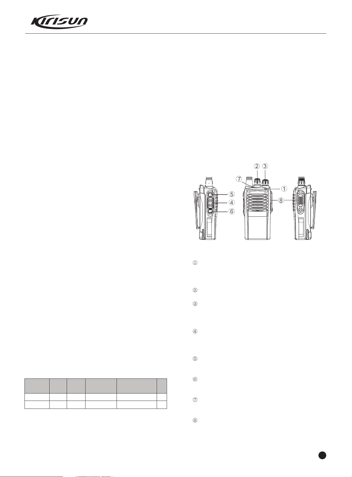
2.1 Radio Overview
Figure2-1
LED Indicator
Lights red while transmitting signals; lights green while receiving
signals.
Flashes red while in low battery power during transmitting.
Channel Selector
Rotate it to select channel 1-16.
Power/Volume Switch
Turn clockwise till a click is heard to switch on the radio.
Turn counterclockwise till a click is heard to switch off the radio.
Rotate it to adjust the volume after turning on the radio.
PTT (Push-to-talk)
To make a call, press and hold the PTT button, then speak into
the microphone in normal voice.
Release the PTT button to receive a call.
Side key 1
Programmable function button: Press it to activate the
programed auxiliary function.
Side key 2
Programmable function button: Press it to activate the
programed auxiliary function.
Top Button
Programmable function button: Press it to activate the
programed auxiliary function.
Microphone/Speaker Jacks
For connecting the optional Microphone/Speaker.
1
Page 4
PT7200 SERVICE MANUAL
Chapter 3 Electrocircuit
3.1 Frequency Configuration
This radio receiver adopts the 2 Mixer, the 1 IF 51.65MHz,
nd
the 2 IF 450kHz.
The receiver's first local oscillation is generated by the
frequency synthesizer, the 2 local oscillation selects the 4
harmonic wave 51.2MHZ of TCXO.
The transmitter signal is generated by the
synthesizer.
The standard frequency of the frequency synthesizer is
generated by TCXO.
Figure 3.3 Frequency structure
nd st
nd th
frequency
3.2 Receiver Elements (RX)
as the 2 local oscillation signal source after amplification. The 2
local oscillation (51.2MHz) and the 1 IF signal (51.65MHz) are
mixed at U9 to generate the 2 IF (450MHz). After the 2 IF signal
nd nd
st
nd nd
is amplified and its amplitude is limited inside U9, and then filtered
at porcelain filter (wideband CF4/Nattowband 3, 450kHz) and then
sent to U9 to demodulate the output audio signals which are finally
output from the 9 pin of U9.
th
Figure 3.5 IF System
Receiver Audio Signal Processing
IC13, IC12, IC16, IC15 and their peripheral circuit compose the
receiver audio signal processing circuit. After being sent to IC13
from U9 for amplification Audio, the audio signal is sent to IC15
CTCSS signaling filter circuit for waveform shaping and then sent to
MCU; and it is simultaneously sent to IC12 and through IC12
amplification, deemphasis, filtration to remove high frequency and
low frequency elements in the audio, only audio components of
300--3000Hz are kept to be sent to audio power amplifier (U9) after
volume potentiometer adjustment, and simultaneously sent to MCU
through IC15 (2 tone/5 tone filtration circuit).
Figure 3.4 Receiver Illustration
The receiver front terminal
Signals from the antenna pass through the low pass filter
consisting of L104, C546, L103, C545, L102, C534 and the RX/TX
switch (D51); and then undesirable out-of-band signals will be
filtered out at the band pass filter (BPF) consisting of L104, C546,
L103, C545, L102, C534; then signals are amplified at the low noise
amplifier (LNA) consisting of Q81 and its peripheral components.
The output of LNA is sent to the first mixer (Q79) through the
BPF filter consisting of L115, C541, D63, C528, C591, L114, D62,
C527, C590, L113, D60 and C526.
The First Frequency Mixer
After mixing the receiving signals and the first local oscillation
signals from the frequency synthesizer, the 1 IF signals (51.65MHz)
are generated. The 1 IF signals pass the crystal filter (XF2), which
st
st
will filter the signals of adjacent channel and those out of band, and
are sent to the IF amplifier.
IF Circuit
The IF signals from the crystal filter are amplified at the 1 IF
st
amplifier (Q78), and then are sent to the IF processing IC (U9,
TA31136FN). The IF IC consists of the 2 frequency mixer, the 2
nd nd
local oscillator, IF amplifier, limiter, phase frequency detector, and
noise amplifier.
TCXO (X4, 12.8MHz) selects the 4 harmonic wave 51.2MHZ
th
2
Figure 3.6 Receiver Audio Processing
Squelch Circuit
The audio signal output from the demodulation of U9 is sent
back to U9 internal noise amplifier and composes the frequency
selection noise amplifier together with C320, Q77, R167, C439 and
C319. Filtered from the demodulation signals, the noise is changed
into DC level by D57 demodulation after amplification by Q77 and
then sent to MCU, which distinguishes the noise volume so as to
decide whether to enable the squelch, which achieves the control of
the squelch.
Audio Power Amplifier
Q92 and peripheral compose the BTL-audio and power
amplifier.
The audio receiving signals, voice indication signals, indication
tone signals and warning tone signals are converged to be
amplified by the audio power amplifier to drive the speaker.
Speaker impedance: 16Ù
Q95: Receiving audio signal switch
Note: No terminal of the speaker can be grounded!
CTCSS signaling filter
The U9 Demodulation output audio signals may contain CTCSS
(continuous tone coded squelch system) or DCTCSS (Digital coded
squelch) signals. The frequency spectrum of CTCSS/DCS is 20250Hz. The filtering circuit constructed by IC16can filter out the
signals out of the CTCSS/DCS frequency spectrum to ensure MCU
Page 5
to decode CTCSS/DCS more precisely.
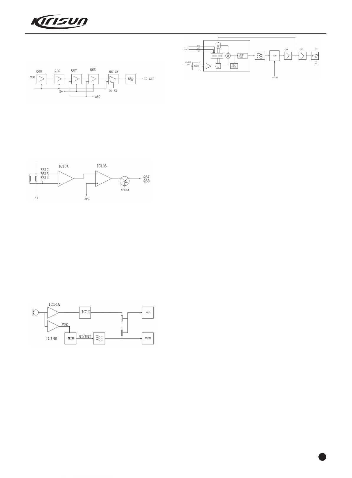
3.3 Transmitter (TX)
Transmitter Power Amplifier
Figure 3.7 Amplifier and antenna switch diagram
The modulated RF signals from VCO are amplified at Q60, Q66,
Q67 and then are sent to Q68 for power amplification. Q68 output
power: 4.5W.
The Q67, Q68 grid offset is controlled by APC circuit. Changing
the grid bias can control the transmitter output power conveniently.
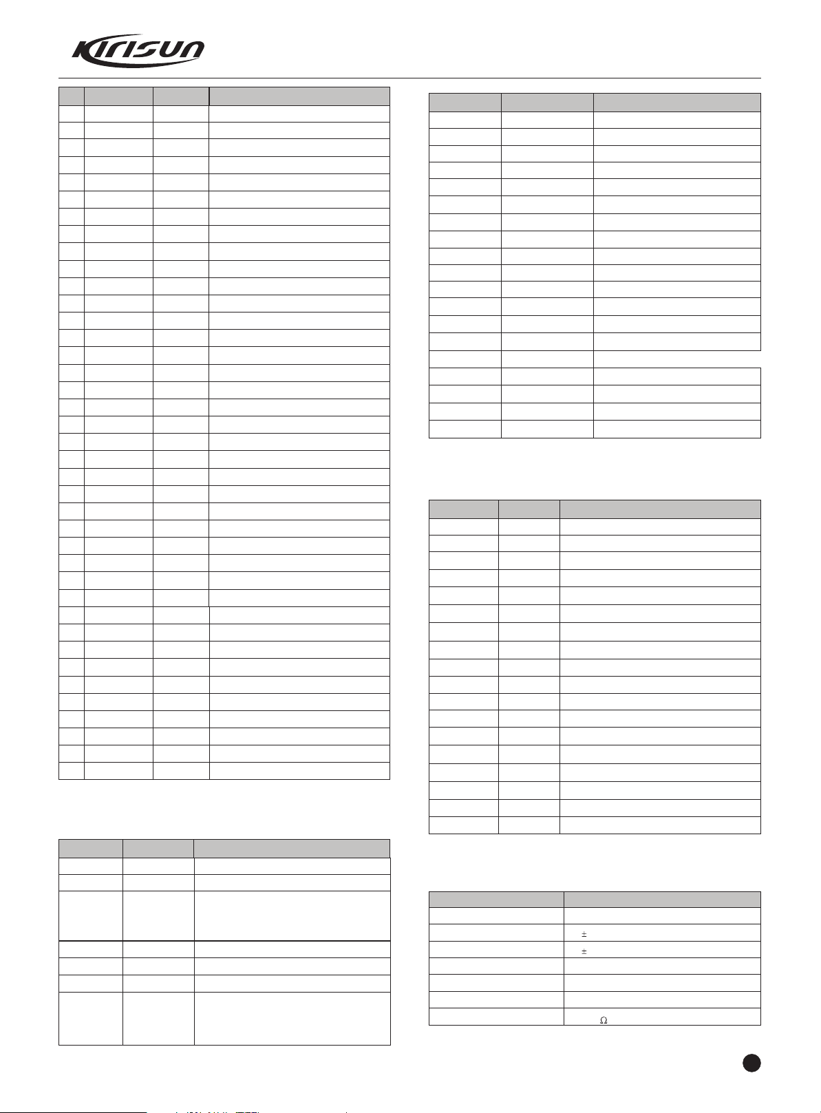
APC (Auto Power Control)
Figure 3.8 APC Circuits
R512, R513, R514 are the amplifier current checker; IC10A the
sample amplifier of the amplification current. IC10B is the power
comparison amplifier.
If the transmitter output power is too high, the amplifier current
will increase, IC10A output will mount, IC10B output voltage
decrease, the offset voltage added to Q67 and Q68 will decrease,
and then the transmitter output power will decrease. Vice versa,
such can ensure steady transmitter output power in different
working circumstances.
MCU changes the voltage input to IC10B to set the power.
Transmitter Audio Signal Processing
PT7200 SERVICE MANUAL
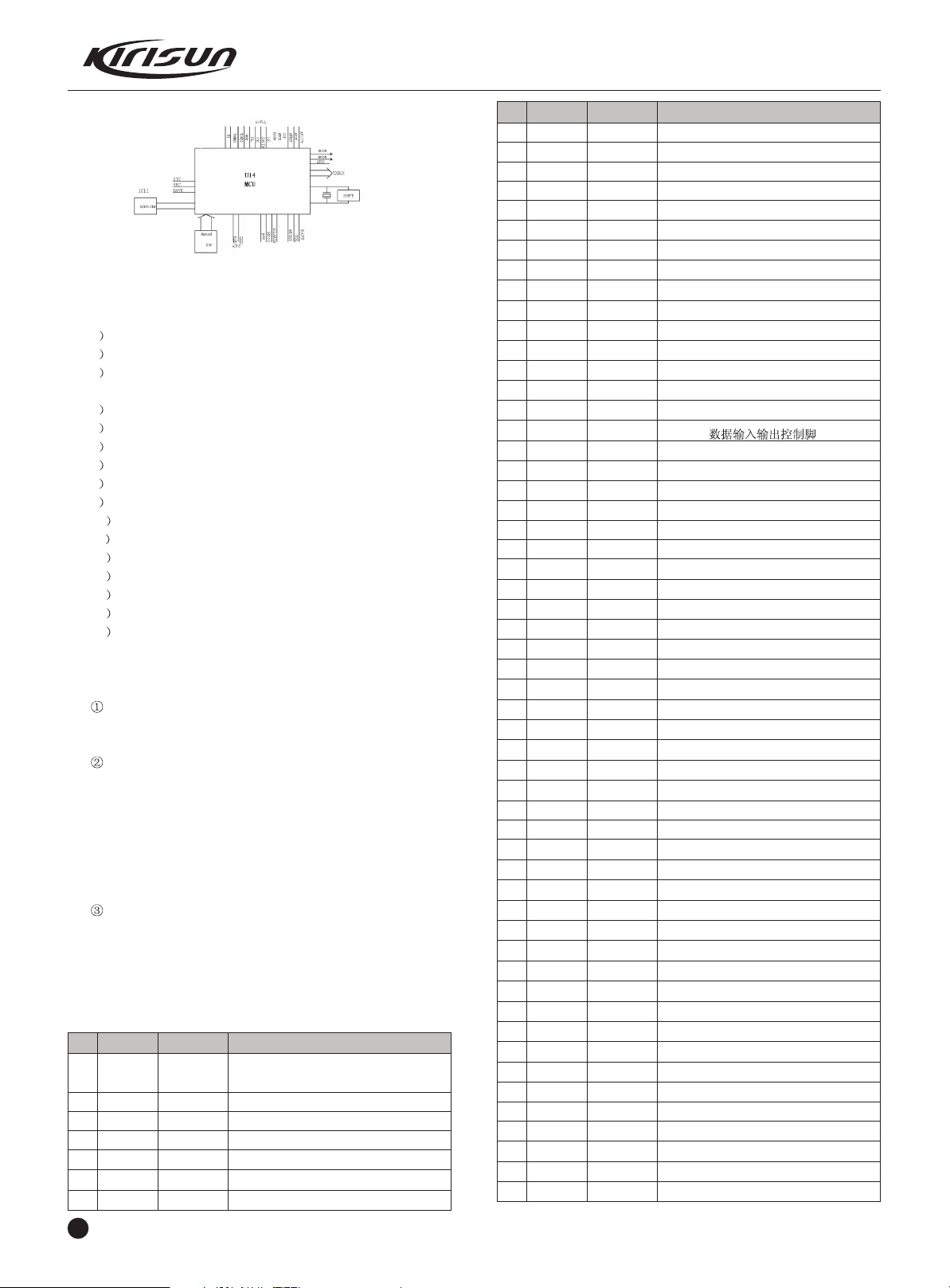
Figure 3.10 Frequency Synthesizer
The radio adopts Phase Locked Loop (PLL) frequency
synthesizer.
The frequency synthesizer consists of standard oscillator,
voltage controlled oscillator (VCO), programmable frequency
demultiplier, phase comparator, and low pass filter.
IC9 (ADF4111) is PLL integrated circuit, including
programmable reference frequency demultiplier, programmable
frequency demultiplier, phase comparator, and charge pump.
R334, C464, R333, R311, C448, C484 and R336 construct the
low pass filter.
The standard frequency is supplied by X4 (TCXO, 12.8MHz).
The standard frequency from TCXO (Temperature Control
Transistor Oscillator) is demultiplied by the programmable reference
frequency demultiplier at IC9 to acquire 6kHz or 6.5kHz reference
frequency (controlled by MCU according to the preset channel
frequency).
The oscillation frequency from VCO is sent to IC1, and
demultiplied by programmable frequency demultiplier and
compared with reference frequency to acquire the error signals.
Then pass the low pass filter and are sent to VCO to change VCO
oscillation frequency to the preset value, and then VCO is locked.
N=F /F
N: Frequency demultiplication times
F : VCO oscillation frequency
F : Reference frequency
Check Loss of Lock: When PLL is in loss of lock, IC pin14
sends out low level signals to MCU, which controls the transmitter
not to transmit and initiate warning tone.
3.5 Voice Prompt Circuit:
The radio features voice prompt, which is very useful at night or
in the environment of dim light.
The internal memory IC of MCU is provided with voices like
channel indication, etc., each time switch a channel, the speaker
will prompt the current channel number by voice prompt.
VCO R
VCO
R
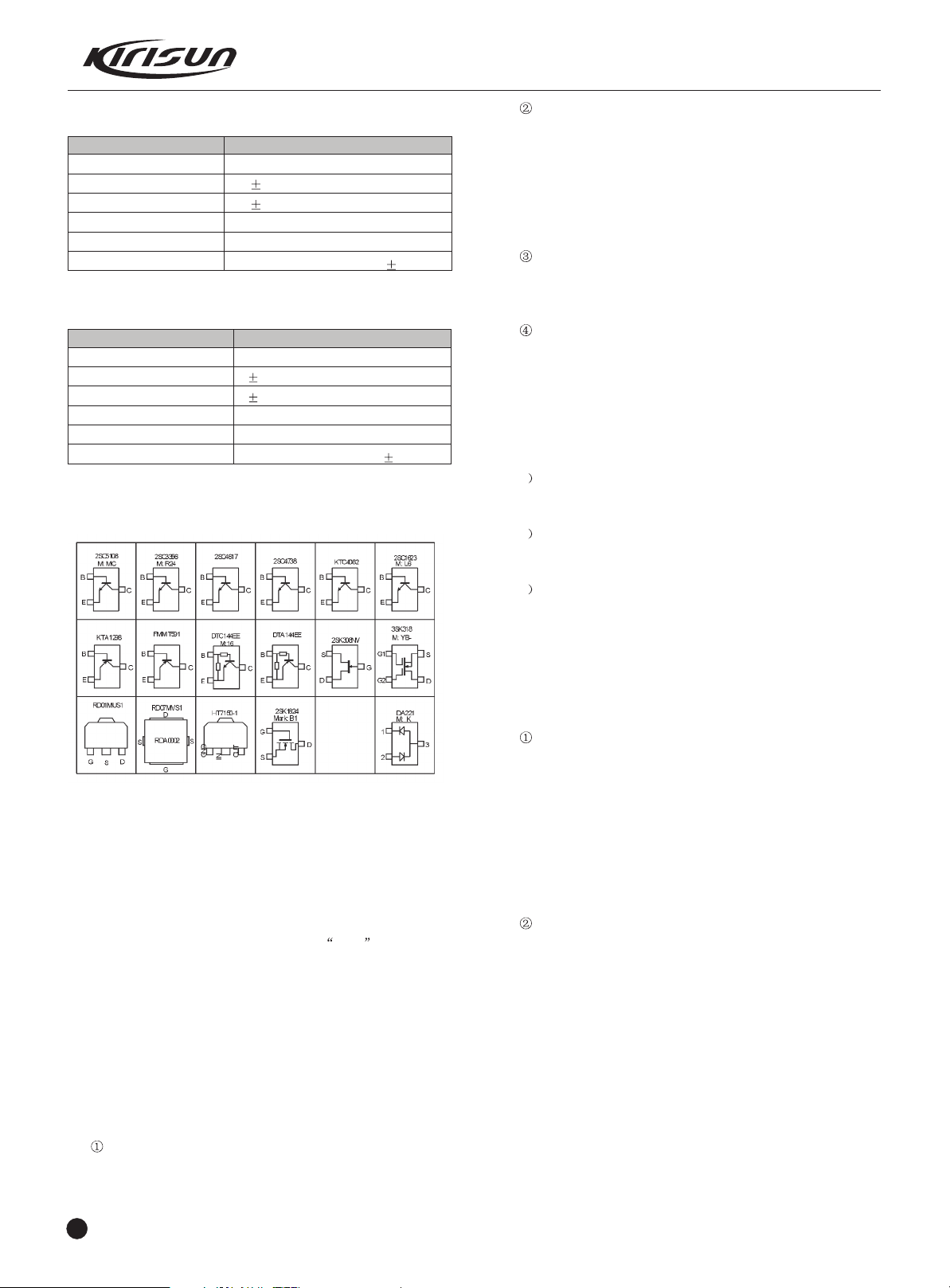
Figure 3.9 Transmitter Audio Circuits
IC14, IC12 and the peripherals components compose the
transmitter audio processing circuit. The audio signals from MIC are
amplified to be sent to MCU after the demodulation (VOX signal);
simultaneously they are amplified after preemphasis, amplitude limit
and filtration in the C12 where they have been sent there through
the ACC circuit and finally sent to VCO modulation together with
CTCSS/DCS for modulation.
J2 is the external MIC socket, when the external MIC is used,
the internal MIC will be off automatically while the internal PTT will
remain activated.
3.4 Frequency Synthesizer
3.6 Power Supply:
The radio is equipped with 7.4V, 1700mAh li-polymer battery,
transmitter power amplifier circuit (Q67, Q68), receiver audio power
amplifier (Q92) directly adopt the power supplied by the battery and
other circuits adopt the regulated 5V to supply power.
U13: 5V low voltage difference, micro-power regulator, together
with U12 to supply 5V power with high current.
Q76: T5V switch, controlled by MCU.
T5V: Supply power for the Transmitter front terminal
Q85: R5V switch, controlled by MCU.
R5V: Supplies power for the receiver RF amplification, mixing,
IF processing, audio signal processing.
Q83: C5V switch, controlled by MCU.
C5V: The 5V power controlled by power saving supplies power
for the frequency synthesizer.
3
Page 6
PT7200 SERVICE MANUAL
3.7 MCU:
Figure 3.11 MCU Diagram
MCU controls the working of each unit of the radio to realize
all the radio functions.
1 Connects with the PC
2 Accesses the radio status data
3 Controls PLL to generate the receiving and transmitting local
oscillation frequency.
4 Accesses the current channel status.
5 Controls the LED status indication
6 Controls the power supply of each location
7 Checks the action of each function key
8 Generates voice contents
9 Generates power on voice prompt
10 Generates CTCSS/DCS signals
11 Generates 2 tone/5 tone signals
12 Generates power control signals
13 Completes CTCSS/DCS decoding
14 Completes 2 tone/5 tone decoding
15 Squelch check and control
16 VOX level sampling
Controls the audio processing chips to complete
emphasis/deemphasis, scrambling/descrambling, companding,
filtration and amplification etc.
Memorizer (E PROM, AT24C64)
2
Memorizes the channel data, CTCSS/DCS data as well as
other function setting data and parameter setting data of the radio.
CTCSS/DCS Encoding and Decoding:
CTCSS/DCS signals generated by MCU (pin24, pin28 output,
PWM wave) are filtered at the filter circuit and then sent to VCO and
TCXO modulation respectively.
CTCSS/DCS signals from the receiver are sent to MCU for
decoding. MCU determines whether the signals contain the same
CTCSS/DCS as that set on the radio and decides whether to turn
on the speaker.
Power adjustment:
MCU PIN1 output DC signals, inputted to APC unit to control
the output power of the transmitter.
3.8 Semiconductor Component
MCU Description
Table 3.3 Microprocessor (M30620FCPFP) Port Description
PinNo. Port Name
1 PCTV
2 DTMF
3 HSDI
4 EPDT
5 EPCK
6 BYTE
7 CNVSS
Input/ output
D/A Output
D/A Output
I
I/O
O
I
I
Function
Receiver sensitivity adjusting voltage
output/power control (V)
DTMF/Tone output, beep output
Tone decoding input
EEPROM data input/ output
EEPROM clock
Gnd
Gnd
4
PinNo. Port Name Input/ output Function
8 BSHIFT
9SV
10 RESET
11 XOUT
12 VSS
13 XIN
14 VCC
15 NC
16 VDET
17 RDT
18 TCLK
19 SCLK
20 QT/DQT
21 TDATA
22 StCtrl
23 DI/O
24 QTVCO
25 DIR
26 APC
27 NC
28 QTTCXO
29 TXD
30 RXD
31 NC
32 APC SW
33 TXD0
34 RXD0
35 DC SW
36 TX W/N
37 RX SW
38 TX SW
39 NC
40 PLL UL
41 PLL STD
42 PLL DATA
43 PLL CLK
44 NC
45 RX W/N
46 EN1
47 EN2
48 EN3
49 EN4
50 EN5
51 W/N R1
52 W/N R2
53 AFCON
54 RX MUTE
55 A BUSY
56 A DATA
57 A SCLK
58 A MUTE
59 NC
60 ACC
61 NC
O
Clock beat frequency control
O
Min. volume control
I
CPU reset input
O
CPU reset output
-
Gnd
I
CPU clock input
-
+5V
I
+5V
I
Voltage down detection
I
AK2346 MSK signal input
I
AK2346 MSK data transmission clock
O
AK2346 data transmission clock
I/O
CTCSS/DCS output
O
AK2346 MSK data transmission outp ut
O
Side tone volume control pin
I
AK2346
O
CTCSS/DCS output VCO (PWM)
O
AK2346 IO control
O
Power control (U)
-
NC
QT/DQT TCXO (PWM)
O
O
TXD1 output
I
RXD1 input
NC
-
O
Power control output switch
O
Extension
I
Extension
O
Power control switch
O
Transmission bandwidth switch
O
Receiver VCO switch
O
Transmitter VCO switch
Gnd
I
Phase-locked loop loss of lock check pi n
O
Phase-locked loop enabling control
O
Phase-locked loop data output
O
Phase-locked loop clock
-
NC
O
Receiving bandwidth switch
I
UV band selection
I
Encoding switch input pin
I
Encoding switch input pin
I
Encoding switch input pin
I
Encoding switch input pin
O
Receiving IF bandwidth switch
O
Receiving IF bandwidth switch
O
Audio power amplifier enablingcontrol
O
Receiving mute switch
I
Number reporting chip control
O
Number reporting chip data output
O
Number reporting chip clock
O
Number reporting chip control
-
NC
-
+5V
-
NC
Outputs
Page 7
PT7200 SERVICE MANUAL
PinNo. Port Name Input/ output Function
62 VSS
63 NC
64 SELF
65 OPT S1
66 OPT S2
67 PIO3
68 PIO2
69 PIO1
70 PINT
71 TK1
72 PTT
73 Sk2
74 SK1
SP SW
75
MIC SW
76
R LED
77
G LED
78
5T C
79
5R C
80
5C C
81
P03
82
P02
83
NC
84
NC
85
MAN DOWN
86
BATT
87
RSSI
88
BUSY
89
VOX
90
QT/DQT IN
91
DTMF IN
92
AVSS
93
NC
94
VREF
95
AVCC
96
NC
97
MIC MUTE
98
MIC MUTE
99
HPF PC
100
-
-
-
I
I
I/O
I/O
I/O
I
I
I
I
I
O
O
O
O
O
O
O
O
O
O
-
I
I
I
I
I
I
I
-
-
-
-
-
O
O
O
Gnd
NC
Factory control options
Earphone check
External PTT
MAN DOWN input
Extension
Extension
Extension
Extension
Top key
PTT key
Side key 2
Side key 1
Speaker switch
MIC switch
LED red switch
LED green switch
5T control pin
5R control pin
5C control pin
Fixed side tone control
Phase-locked loop filter
NC
NC
Reverse detection input
Voltage check input
Receiving filed intensity signal input
Squelch voltage check input
VOX voltage check input
CTCSS/DCS input
DTMF input
Gnd
NC
+5V
+5V
NC
External and internal MIC switch
High pass filter switch
Table3.4: Semi-Conductor Component Function
Location mark Model
Ic9 ADF4111
Ic10 NJM2904
U9 Ta31136
Ic12 AK2346
IC14 TC75W51FU
Q92 TDA8541
Ic11 AT24C64
Function description
Phase-locked loop chip
APC, voltage comparison, drive
Receiver's 2nd local oscillation, 2nd IF
amplifier, amplitude limit, demodulation ,
noise amplification
Audio processing
MIC amplification
Receiver audio power amplifier
E2PROM, memory channel frequency
data, function setting parameter,
debugging status parameter
Location mark Model Functiondescription
U14 M30620FCPFP
U11 PST9140NR
Q60 2SC5108
Q66 2SC3356
Q56 2SC5108
Q57 2SC5108
Q65 2SC4617
Q77 2SC2412K
Q68 RD07MVS1
Q67 RD01MUS1
Q69 DTA144EE
Q79 3SK318
Q81 3SK318
Q78 2SC5108
Q73 DTC144EE
Q74 DTC144EE
Q83 2SJ243
Q76 2SA1745
Q85 2SJ243
MCU
MCU reset circuit
Transmitter 1st amplification
Transmitter 2nd amplification
VCO buffering amplifier
VCO buffering amplifier
VCO power filter
noise amplifier
Transmitter final amplifier
Transmitter amplifier drive
APC output switch
The first frequency mixer
Receiver HF amplifier
The first IF amplifier
Red LED drive
Green LED drive
C5V switch
T5V switch
R5V switch
Table 3.5 Diode Function Description
Location mark Model
D Ma77
D101 HSC277
D103 HSC277
D104 HSC277
D201 HSC277
D302 MA2S376
D304 MA2S376
D305 MA360
D310 MA2S376
D308 MA2S376
ZD12 HZU5ALL
D38 MA2S111
D48 MA2S111
D57 1N4148
D53 LED RED
D55 LED GREEN
D54 LED RED
D56 LED GREEN
Function Description
Transmitter antenna switch diode
VCO output switch
Antenna switch
Antenna switch
VCO output switch
VCO oscillation variable capacitance diode
VCO oscillation variable capacitance diode
VCO modulation diode
VCO oscillation variable capacitance diode
VCO oscillation variable capacitance diode
APC output voltage-limiting diode
Loss of lock check diode
VCO power filtering accelerating diode
Noise detector
Transmitting indication
Receiving indication
Transmitting indication
Receiving indication
Table 3.6: XF203 crystal filter features
Item
Nominal center frequency
Transmission bandwidth
40dB barrage bandwidth
Pulse
Insertion loss
Guarantee attenuation
Terminal resistance
Rated value
51.65MHz
7.5kHz or bigger within 3dB
20.0kHz or smaller
1.0dB or smaller
3.0dB or smaller
80dB or bigger within fo-910kHz
1.5k /6PF
5
Page 8
PT7200 SERVICE MANUAL
Table 3.7 CF201 LTWC450F functions and features
Item
Nominal center frequency
6Db bandwidth
50dB bandwidth
Pulse
Insertion loss
Guarantee attenuation
Rated value
450kHz
5.0kHz or bigger
13.5kHz or smaller
3.0dB or smaller
7.0dB or smaller
45.0dB or bigger within f0 100kHz
Table 3.8 CF202 LTWC450G functions and features
Item
Nominal center frequency
6Db bandwidth
50dB bandwidth
Pulse
Insertion loss
Guarantee attenuation
Rated value
450kHz
3.5kHz or bigger
12kHz or smaller
3.0dB or smaller
7.0dB or smaller
45.0dB or bigger within f0 100kHz
Table 3.9 Semiconductor Component Packaging
Illustration:
Chapter 4 Function Description and Parameter Set ting
4.1 Major Functions
4.1.1 16 Channels
The radio stores 16 channels.
4.1.2 Scanning Channel Function (this function can be
disabled by the programming software)
1) Press the key set to the function of scan to enter the
scanning function. During the scanning, the radio will check signals
of each channel to the signal is found, and then the radio will stay
on the channel with signals till the signal disappear. If the time delay
between the signals disappearing and the scan is set, the radio will
remain on the channel when any signal is received during the
delayed time.
The scanning function can be used only when at least one
channel is programmed and the scanning is valid.
2) Response channel (the transmitting channel when scanning)
during the scanning set by the dealer has the following options:
. The start channel
Press PTT or the CALL key or enable VOX transmitting during
the scanning or when the scanning stays, the radio will transmit
signals on the channel under scanning.
6
. Start channel + current channel (when response channel is
enabled)
If pressing PTT or the CALL key or enabling VOX transmitting
during the scanning, the radio will transmit signals on the channel
under scanning.
If pressing PTT or the CALL key or enabling VOX transmitting
when the scanning is staying, the radio will transmit signals in the
current channel.
. Designated channel
If pressing PTT or the CALL key or enabling VOX transmitting
during the scanning or when the scanning stays, the radio will
transmit signals in the designated channel.
. Designated channel + current channel (when response
channel is enabled)
If pressing PTT or the CALL key or enabling VOX transmitting
during the scanning, the radio will transmit signals at the designated
channel.
If pressing PTT or the CALL key or enabling VOX transmitting
when the scanning is staying, the radio will transmit signals in the
current channel.
1 . Last received call channel
When pressing PTT key, the radio will transmit signals on the
channel of the last received call.
2 . Last used channel
When pressing PTT key, the radio will transmit signals on the
channel where the last transmitting was made.
3 . Last used channel + current channel (when response
channel is enabled)
If pressing PTT or the CALL key or enabling VOX transmitting
during the scanning, the radio will transmit signals on the channel
where the last transmitting was made.
If pressing PTT or the CALL key or enabling VOX transmitting
when the scanning stays, the radio will transmit signals in current
channel.
Priority scan:
During the scanning, if priority channels of the radio have been
set, even if the normal channels are receiving signals, the radio will
scan the priority channels according to the preset time of scanning,
when the priority channels receive signals, the radio will
automatically switch to the priority channels and stay there till the
signals disappear, the dealer has set the time delay between the
signal disappearing and the continuing scanning, if the scanning
stays on 2 priority channel, it will scan back 1 priority channel, on
nd st
which if it stays, no channel will be scanned back.
Excrescent channel (temporary) deletion
If the scanning stays on a certain channel, you can press the
key programmed for deletion of excrescent channel (temporary) to
temporarily delete the channel for the scan list, if you press the
scan key to resume the scanning, this channel will be automatically
added into the scan list again.
Note: priority channels cannot be deleted, when there are only
2 channels for scanning, neither of them can be deleted.
4.1.3 CTCSS and DCS
The dealer may have programmed CTCSS or DCS signals on
channels of the radio, you can ignore calls from other irrelevant
stations using the same channel.
If a certain channel is programmed CTCSS or DCS signals,
only when the correct CTCSS or DCS signals are received can the
squelch be enabled. Similarly, only stations using the same
Page 9
PT7200 SERVICE MANUAL
CTCSS/DCS signals as being used in your radio can receive the
signals you transmit.
4.1.4 TOT function
1) TOT timer:
a) The purpose of the time-out timer is to prevent any person
from overlong using a channel to speak and to prevent radio from
too long continuous transmitting.
b) TOT timer indicates the time allowed for the radio to
continuously transmit signals. If the allowed time is exceeded, the
radio will alarm and stop transmitting.
2) TOT key:
a) It regulates the time span of prohibited transmitting after the
action of the TOT timer.
B) During the time span of prohibited transmitting, if pressing
the PTT key or the CALL or starting the VOX, indication tone will be
generated and the transmitting will be prohibited.
3) TOT Pre-alarm
a) The radio will alarm in advance before the TOT timer stops
the transmitting.
b) After the alert, if the transmitting time exceeds the preset
time, the TOT timer will act.
4) TOT Reset:
a) It regulates the time delay from PTT key releasing to the TOT
timer resetting.
b) If the time of releasing the PTT key is shorter than that of the
resetting time, the countdown will continue.
4.1.5 Auto Power Saving
The dealer can set the power-saving mode of the battery by
programming.
Provided that the function is enabled, the radio will be in the
power-saving mode in 10 seconds if no signal is received or no
operation is carried out. When any signal is received or any
operation is carried out, the radio can automatically quit this mode.
Power-saving modes: short, med, long and off.
Setting the power-saving function of a battery can reduce the
power consumption of the battery.
4.1.6 Low Power Warning
Receiving low power warning: If the battery power is lower than
the preset value during receiving, the radio will produce a alert tone
of Doo every 15 seconds.
Transmitting low power warning: When the battery power
appears low, the indicator flashes. If the battery power is lower than
the preset value during transmitting, the status indicator flashes red.
If the battery level is too low, the radio cannot transmit signals.
4.1.7 Squelch enabled function
If no signal is received, the squelch circuit of the radio will
prevent the speaker from making any sound.
Press the function key for squelch off switch , you can disable
the squelch control circuit and the speaker will produce continuous
sound (whether signals are received). This operation is very useful
for adjusting volume or receiving weak signals (avoiding
discontinuous sound due to weak signals).
Press the function key for squelch on switch , the green light
will be on and the radio is in the monitoring status.
4.1.8 5TONE signaling
5Tone has 9 encoding formats: CCIR1, CCIR2, ZVEI1, ZVEI2,
ZVEI3, EEA, EIA, USER DEFINED1 and USER DEFINED2. The
last two formats are customized modes.
1. 5tone decoding
The decoding template is the 5tone decoding template. If the
decoding template is the same to that of encoding, the decoding will
be successful.
When the radio receives correct 5tone signaling, turning on
squelch according to the receiving squelch mode set by the user,
you can receive the call and the orange LED will flash.
After successful decoding, the radio will operate according to
the decoding call response set by the dealer.
2. 5tone encoding
The ending template is made of 1-3 encoding sequences. Each
encoding sequence can be set to 5tone or DTMF. If 5tone is
selected, you need to set its content.
If the PTT ID of the selected channel is set to 5Tone , 5Tone
will be transmitted when calling.
Or, when pressing the side key for Call1/2/3/4 , 5tone
signaling will be sent, this function is programmed by the dealer.
4.1.11 PC Programmable
You can program the radio functions and adjust some
parameters by PC programming software KSP7200.
4.1.12 Squelch Level Selection
The purpose of the squelch is to mute the speaker noise when
no signals are received or the signals are weak. When the squelch
is activated, you can hear noise from the speaker; when the
squelch is inactivated, you will not hear noise form the speaker.
Selecting the squelch level is to select which the signal strength
level is strong enough to enable the squelch or weak enough to
disable the squelch. Over high squelch level will make the radio
unable to receive signals efficiently when signals are weak; over low
squelch level will make the radio communication affected by noise
or other irrelevant signals. The squelch level has 0-9 options..
4.1.13 Beep Tone Volume
This setting controls the power on tone, channel busy tone and
TOT tone, etc..
4.2 Parameter Setting (PC Mode)
The radio parameters have been programmed in the factory.
The user can reset the radio parameters such as working frequency,
channels, CTCSS/DCS and auto scanning. We designed a userfriendly and convenient programming software KSP7200 for users
to set parameters on the radio. The programming steps are as
follows:
a. Install the programming software KSP7200.
b. Connect the radio to the computer serial port with the
specified programming line (KSPL-08), See Figure 4-1.
Computer
(RS232 serial port)
Figure 4-1
c. Turn on the computer power.
d. Turn on the radio power.
e. Click the KSP7200 program to run the programming software.
Programming
cable
Radio
(Speaker/MIC socket)
7
Page 10
PT7200 SERVICE MANUAL
f. Click on [Read] in the KSP7200 main menu to read the radio
parameters into the computer; click on [Write] to transfer the PC
programming parameters into the radio.
g. You can program the following parameters with the KSP
7200:
1) The RX and TX frequency of each channel;
2) The receiving and transmitting signaling of each channel;
3) Busy channel lockout option;
4) TOT;
5) Squelch level option;
6) 5-tone or 2-tone settings
7) Power saving option.
8) Alarm function setting.
9) Monitor mode option.
10) Scan mode option.
11) Scan the reverting channel option.
12) Scan the priority channel selection.
For more details, please refer to the Help document of
KSP7200 software.
ATTENTION:
1. Turn off the radio before connection.
2. When the data is read on the radio, the indicator light turn red
and it's prohibited to press the PTT button; when the data is written
on the radio, the indicator light turns green.
3. Before the first time of editing, you should read data on the
radio firstly and then and backup the data.
4. If the radio cannot work normally after being written in with
the editing data, open the data backup and rewrite the backup into
the radio.
5. Model information is important radio data and is prohibited
to modify.
4.3 Computer Test Mode:
As shown in figure 4-1,connect the radio to the radio
communication port with the specified testing cable.
Warning: Before enter the computer test mode, connect a HF
load of 50 to the radio antenna connector or connect the radio to a
comprehensive test device.
Under the computer test mode, you can modify the following
parameters with KSP7200 programming software:
1) Frequency Stability
2) Low/High power
3) Max. Tone deviation
4) DCTCSS balance
5) DCTCSS frequency deviation
6) CTCSS frequency deviation
7) DTMF frequency deviation
8) Tone frequency deviation
9) MSK frequency deviation
10) VOX plus
11) Sensitivity
12) SQL 1/9 (OPEN/SQUELCH)
For mort details,please refer to the Help document of
ksp7200 software.
4.4 Wired Clone Parameters
Wired clone mode:
It can be enabled/disabled by programming software, this mode
can only be entered when the wired clone functions of both the host
radio and the client radio are enabled.
Operating steps are as follows:
1.Press the side keys SK1 and SK2 of the primary, and then press
and hold the power switch of the radio for about 2 seconds, the
orange light flashes twice and the beep sound of Clone will be
produced, and then the radio enters the wired clone mode.
2.Press the PTT button on the host radio, the host radio will start to
send data, the client radio for receiving data will enter the wired
clone mode.
3.During the data duplication, the red light of the host radio will be
continuously on and the green light of the client radio will be
continuously on.
4.After the data are successfully cloned, the host radio will report
Success and be automatically restarted; the client radio will
also be automatically restarted.
Note: During the duplication of data, if the radio models or software
versions are not consistent, the red light of the host radio will flash
(0.25s On 0.25s Off) and the sub radio will be automatically
restarted; if no data was received within 3 seconds, the red light of
the host radio will flash (0.5s On 0.5s Off) and the client radio will be
automatically restarted.
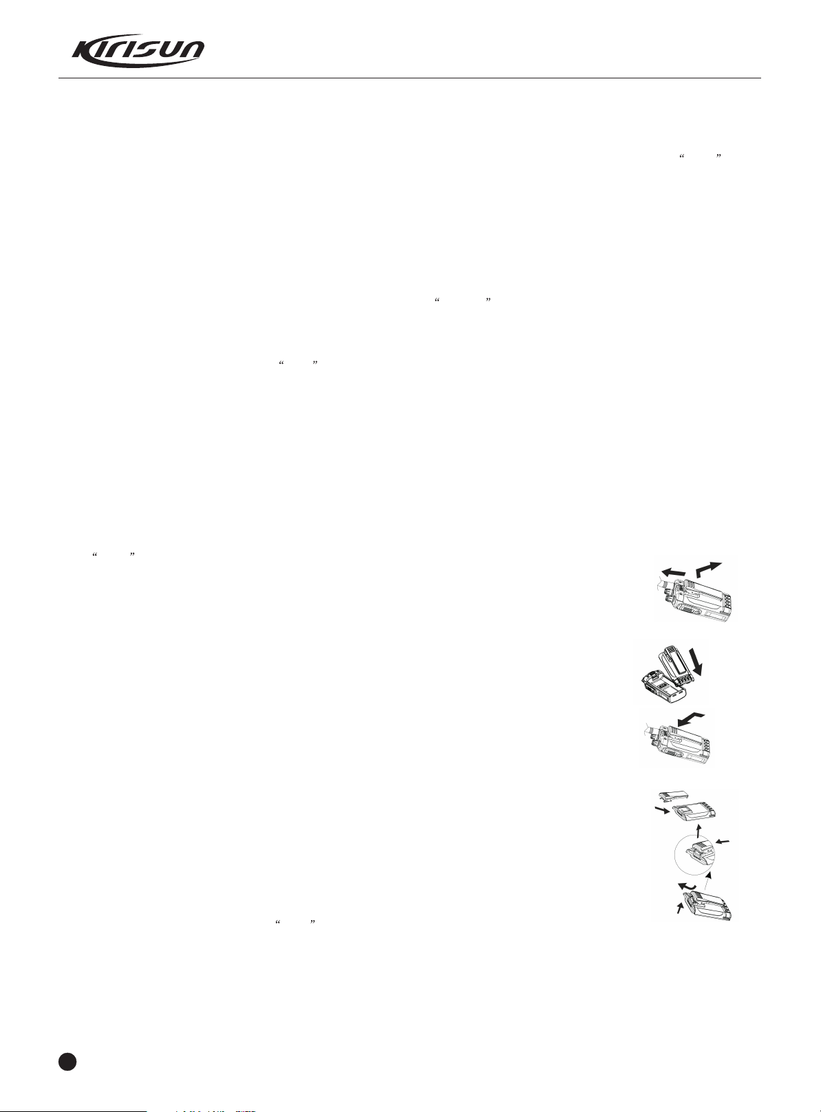
Chapter 5 Service, Assembly and Disassembly
The radio is a precision communication equipment. Please be
careful when assemble or disassemble the radio during service.
Instructions for assembly and disassembly are as follows:
5. 1 Removing and Installing
the Battery
To remove the battery, push the
latch upwards and remove the
battery away from the radio. (See
figure 5.1)
To install the battery, match the
tow bulges at the bottom of the
battery with the corresponding
grooves at the radio aluminum alloy
frame and insert it in. Then press the
upper end of the battery till the latch
secure. (See figure 5.2 and figure
5.3)
5. 2 Removing and Installing
the Belt Clip
To remove the belt clip, use
your nail or a tool to lift the metal
spring piece in the belt clip from the
topside, and then pull the belt out
wards.
To install the belt clip, match the
upper head of the belt clip with the
glides on the rear of the battery, and
then press the belt clip downwards
Figure 5.4
Figure5.1
Figure5.2
Figure5.3
8
Page 11
5. 3 Removing the Casing from
the Chassis
1.Remove the knobs;
2.Remove the two knob nuts and
the antenna nut;
3.Remove the two cross head
screws that fix the top cover at the top;
4.Remove the two cross head
screws that fix the aluminum alloy
frame at the bottom by tool;
5.Pull the aluminum alloy frame
out of the casing;
See Figure 5-5
Figure5-5
PT7200 SERVICE MANUAL
5. 4 Remove the Chassis
from the Main Board
1.Remove the screw;
2.Melt the solder at the antenna
point with a electric soldering iron and
take off the main board;
3.Take away the two screws and
the antenna connector..
See Figure 5-6
After the aforesaid operations, you can carry out corresponding
service or debugging according to the actual situation.
5-6 Figure
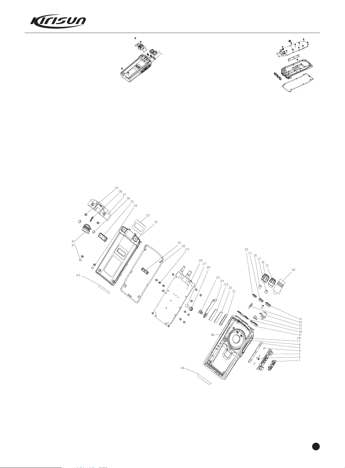
Figure 5-7 Exploded View
9
Page 12

PT7200 SERVICE MANUAL
NO PART NUMBER DESCRIPTION NUMBER
1
2
3
4
5
6
7
8
9
10
11
12
13
14
15
16
17
18
19
20
21
22
23
24
25
26
27
28
29
30
31
32
33
34
35
36
37
38
39
40
41
42
201-007200-R04
301-20040G-R01
202-007200-R04
203-007200-R04
101-007200-R03
201-007200-R01
121-100000-R18
204-000558-R01
202-007200-R03
202-007200-R02
202-007200-R05
203-007200-R01
201-007200-R10
203-007200-R07
201-007200-R03
201-007200-R02
203-006800-R26
203-003208-R09
203-007200-R08
203-000558-R02
204-007200-R02
101-072001-R03
204-007200-R01
201-007200-R08
304-30040G-R01
202-000558-R09
204-006800-R06
203-007200-R02
202-007200-R01
201-007200-R09
203-007200-R03
204-007200-R03
301-20080G-R03
202-007200-R06
202-007200-R07
201-007200-R06
203-007200-R06
301-25050J-R01
201-007200-R07
204-007200-R05
KEY PTT
SCREW 2*4
RUBBER KEY PTT
METAL DOME
PCB FOR PTT
FRONT CABINET
SPEAKER
DUST-PROOF NET FOR SPEAKER
WATERPROOF FOR ANTENNA SOCKET
WATERPROOF FOR ENCODER & VR
EMERGENCY RUBBER KEY
ANTENNA SOCKET
LIGHT GUIDER
NUT FOR ANTENNA SOCKET
ENCODER KNOB
VR KNOB
ENCODER CIRCLIP
VR CIRCLIP
ENCODER NUT
VR NUT
EARPHONE ADHESIVE TAPE
EARPHONE PCB
EARPHONE LABEL
EARPHONE COVER
SPECIAL SCREW M3.0*4 ANSI 4-40#
MIC WATERPROOF
DUST-PROOF NET FOR MIC
MIAN PCB
POGO PIN
MAIN WATERPROOF
POGO PIN SOCKET
AL CABINET
AL CABINET SPONGE
SCREW M2.0*8
POGO PIN WATERPROOF
RUBBERY STUFFER
COPING
CROSSBAR SPRING
SCREW M2.5*5
ANTENNA
SLIDE CROSSBAR
SCREW PLATE
1
12
1
1
1
1
1
1
1
1
1
1
1
1
1
1
1
1
1
1
1
1
1
1
1
1
1
1
3
1
1
1
1
2
1
2
1
1
2
1
1
2
Chapter 6 Radio Debugging
Before test/debugging, make sure all the equipments have
been well connected to the ground!
Before test/debugging, make sure the antenna output terminal
has been connected properly to the corresponding devices and
load!
The transmitter output must pass RF power attenuator before
being connected to the standard signal source/ frequency
deviator/frequency spectrum!
When testing the receiver, make sure not to conduct
transmitting operation!
When in debugging/testing/service, make sure static free
measures for human body and equipments.
6.1 Service Equipment and Software.
The following equipments and software in Table 6.1 are
necessary for the service and test of the radio.
Table 6.1 For Test and Service: Equipment and Software
No.
1
Name
Computer
Parameter requirements
Above P2, compatible with IBM
PC, WINDOWS 98/ME/2000/XP
2
Programming
software
Programming
3
Cable
Tunning cable
4
Cloning line
5
DC regulated
6
KSP7200
Order
Output voltage: 7.5V, output current: 5A
power
Measuring rang: 0.5---10W
7
Power
meter
Frequency range: 100MHz500MHz
Impedance: 50Ù
Frequency meter
8
Frequency range: 0.1600MHz
Frequency precision: higher than 1 10
Sensitivity: higher than 100mV
9
Frequency
Deviator
Digital Multimeter
10
Frequency range: DC600MHz
Measuring range: 0-- 5kHz
Input impedance: higher than 10MÙ/V DC, with
the ability of testing voltage, current, impedance
Audio Signal
11
Generator
RF Power
12
attenuator
Standard signal
13
source
Frequency range: 2---3000Hz
output level: 1---500mV
Attenuation: 40dB or 50dB
Supporting power: Higher than 10W
Frequency range: 10MHz---1000MHz
Output level: 0.1uV~32mV (-127dBm~-17dBm)
-6
10
14
Oscillograph
15
Audio voltmeter
Frequency range: DC~20MHz
Test range: 10mV~20V
Test range: 10mV~10V
Page 13

PT7200 SERVICE MANUAL
Recommendation: Equipment in item 6, 7, 8, 10, 11, and 12 can be
replaced by the HP8920 comprehensive test instrument.
6.2 Debugging
1 . VCO:
Receiving:
High end, adjust TC4 to make VCO voltage-controlled
voltage (CV terminal) be 4.2V 0.2V.
Low end, check VCO voltage-controlled voltage (CV terminal)
to be 0.8V.
Transmitting:
High end, adjust TC3, to make VCO voltage-controlled
voltage (CV terminal) be 4.2V 0.2V.
Low end, check VCO voltage-controlled voltage (CV terminal)
to be 0.8V.
2 . Transmitting:
In computer debugging mode
Frequency adjustment
Adjusts the transmitting frequency to within +/-100Hz of the
nominal frequency in the computer debugging mode.
High power adjustment
Adjusts the transmitting power to 3.8-4.6W in the computer
debugging mode..
(5 frequency points including Higher, High, Med, Low, lower)
Low power adjustment
Adjust the transmitting power to 0.8-1.5W in the computer
debugging mode..
(5 frequency points including Higher, High, Med, Low, lower)
Max. frequency deviation
Signal source: MOD:1kHz/120mV LPF:15kHz
Adjust the max frequency deviation in the computer debugging
mode.
3.9kHz---4.6kHz (wideband)
3.2kHz---3.9kHz (median band)
between 1.8kHz---2.4kHz (narrowband)
DCTCSS balance
Signal source: LPF: 300Hz
Adjust DCTCSS balance in the computer debugging mode.
Make the transmitting demodulation waveform be flat square
wave.
CTCSS frequency deviation
Signal source: LPF: 300Hz
Adjust CTCSS frequency deviation in the computer debugging
mode.
0.50kHz---0.85kHz (wideband)
0.50kHz ---0.65kHz (median band)
0.25kHz--0.50kHz (narrowband)
The waveform shall be good.
DCTCSS frequency deviation
Signal source:LPF:300Hz
Adjust DCTCSS frequency deviation in the computer debugging
mode.
0.70kHz ---1.10kHz (wideband)
0.60kHz ---0.85kHz (median band)
0.25kHz---0.50kHz (narrowband)
The waveform shall be good.
DTMF TONE FSK 5T/2T frequency deviation
Adjust DTMF, TONE, FSK and 5T/2T frequency deviation in the
computer debugging mode.
3.2---4.0 kHz (wideband)
3.0kHz---3.6kHz (median band)
1.6---2.4kHz (narrowband)
Transmitting low battery warning
Adjust the transmitting low battery warning in the computer
debugging mode.
Set the power supply voltage at 6.8V, and press start
and then end
3)Receiving :
Sensitivity adjustment
Adjust the sensitivity in the computer debugging mode.
Make the sensitivity of all frequency points the highest
(provided the sensitivity is the highest, the bigger computer
debugging data, the better)
Squelch adjustment
Adjust squelch in the computer debugging mode.
1 9-level squelch on
T he signal level output should be -118dBm (wideband)
-117dBm (narrowband)
Automatically records the corresponding squelch level
2 9-level squelch off
signal level output -120dBm(wideband
-119dBm (narrowband)
Automatically records the corresponding squelch level
1-level squelch on
Signal level output -124dBm (wideband)
-123dBm (narrowband)
Automatically records the corresponding squelch level
3 1-level squelch off
Signal level output -126dBm(wideband)
-125dBm (narrowband)
Automatically records the corresponding squelch level
Note: Voltage for the aforesaid tests: 7.5V +/-0.1V in room
temperature
Frequency range: 350MHz400MHz 400MHz470MHz
450MHz520MHz
Chapter 7 Technical Specifications
7.1 General Specification
Frequency MHz
Modulation
Number of Channels
Channel Spacing
MF
Working Voltage
Working Temperature
Antenna Impetance
Mic Impedance
Battery (Standard)
Dimension (WxHxD)
Weight
7.2 Receiver
136~174MHz 470~512 MHz
400~470MHz 350~390 MHz
16K0F3E/8K0F3E
16
25 kHz W 20 kHz M 12.5 kHz N
1st MF 51.65MHz 2nd MF 450kHz
7.5V +/-0.1V negative grounding
-25 ~ +55
50
2k
Model KB-70B Li-Ion Battery DC 7.4V , 1700mAh
56 mm 102 mm 29 mm
235g With battery and antenna
11
Page 14

PT7200 SERVICE MANUAL
1 . Sensitivity <= -116dBm (0.35uV) (wideband) (narrowband)
Hi, Med, Low frequency points 14dB SINAD
MOD:1kHz, DEV:+/-3kHz (wideband)
+/-1.5kHz(narrowband)
2 . Distortion half audio power <= 8%
Max audio power <= 20%
16ÙSpeaker, BTL output, 1000mW audio power .
MOD:1kHz, DEV:+/-3kHz (wideband)
+/-1.5kHz(narrowband)
3 . Current
a. Static current <= 85 mA
Volume at the min. value, squelch off.
b.1000mW audio power, current <= 500 mA
4 . Audio correspondence (relative to 6dB/octave deviation) +
2dB / -6dB
5 . Adjacent-channel selectivity >=70dB
(Wideband) / >=60dB(narrowband)
6 . Intermediation rejection >=65dB(wideband) (narrowband)
7 . Parasitic suppression >=70Db
8 . Signal-to-Noise Ratio >=40dB(wideband) / >=35dB
(narrowband)
9 . Squelch off: off when signal source level = -125dBm+/
-3 dBm (level-1 squelch )
10. Squelch on: on when signal source level = -123dBm
+/-3 dBm (level-1 squelch )
7.3. Transmitter
1 .output power High power (3.8W---4.6W)
Low power (0.8W---1.5W)
Hi, Med, Low frequency points, MOD:1kHz, DEV:+/-3kHz.
Red light on when transmitting.
2 .Transmitting current High power <= 1.8A low power <=1.1A
3 .Max. frequency deviation
3.9kHz---4.6kHz (wideband)
3.2kHz---3.9kHz (median band)
1.8kHz---2.4kHz (narrowband)
MOD:1kHz/120mv
4 .Modulation Sensitivity
(mic input1kHz/19mv
2.2---3.8kHz(wideband)
1.2---1.8kHz(narrowband)
5 .Transmitting distortion
MOD: 1kHz, DEV: 3kHz < 3%
MOD: 0.3kHz, DEV: 3kHz < 10%
MOD: 0.4kHz, DEV: 3kHz < 5%
MOD: 0.5kHz, DEV: 3kHz < 5%
MOD: 0.6kHz, DEV: 3kHz < 5%
MOD: 0.8kHz, DEV: 3kHz < 5%
MOD: 1.5kHz, DEV: 3kHz < 5%
MOD: 2.0kHz, DEV: 3kHz < 5%
MOD: 2.5kHz, DEV: 3kHz < 5%
MOD: 1kHz/120mv < 15%
6 .CTCSS frequency deviation
0.50kHz---0.85kHz (wideband)
0.50kHz ---0.65kHz (median band)
0.25kHz--0.50kHz (narrowband)
The waveform shall be good.
7 .DCTCSS frequency deviation
0.70kHz ---1.10kHz (wideband)
12
0.60kHz ---0.85kHz (median band)
0.25kHz---0.50kHz (narrowband)
The waveform shall be good.
8 .DTMF TONE FSK 5T/2T frequency deviation
3.2---4.0 kHz(wideband)
3.0kHz---3.6kHz (median band)
1.6---2.4 kHz (narrowband)
9 .Transmitting frequency deviation
nominal frequency +/-200Hz
10 .modulation feature (relative to 6dB/ octave deviation)
+3dB / -3dB
11 .Transmitting harmonic suppression >=70dB
12 .Signal-to-Noise Ratio >=40dB(wideband) / >=
35dB(narrowband)
13 .Frequency stability +/- 2.5ppm
14 .Under voltage indication
Set the voltage at 6.8V, press the ptt key and the red light
Hould flash and no transmitting power .
15 .Starting time of transmitting should be =55ms
Voltage for aforesaid tests: 7.5V +/-0.1V in room temperature
Frequency range:136MHz-174MHz 350MHz--400MHz
400MHz--470MHz 450MHz--520MHz
Chapter 8 Troubleshooting
No.
Problem
Power on
failnre
1
Phase-locked
loop is
unlocked
(Beep sounds)
2
Cannot talk
to or hear
3
other group
Cannot
receive
Signals.
4
Cause and Solutions
A. Battery power may be insufficient. Recharge
or change the battery pack.
B. The power switch is broken, please change it.
C. The CPU is broken, please change it.
D. Turned off remotely, reprogramming is
required.
A. The PLL crystal oscillator X4 is broken,
please change it.
B. The oscillating tube is broken, and please
change it.
C. Phase-locked loop chip IC9 is broken please
change it.
A. Make sure the two communication radios are
using the channel of the same frequency.
B. Make sure the CTCSS/DCS tone is the same
as that of your group members.
C. Out of the effective communication range.
A. The antenna is not well connected, please
screw the antenna again until secure.
B. The high frequency amplification tube Q81 is
broken, please change it.
C. The squelch level is too high and the squelch
cannot be activated. Reset the squelch level
with a computer.
D. Mixer tube Q79 is broken, and please change
it.
E. MF processing chip U9 is broken, please
change it.
Page 15

PT7200 SERVICE MANUAL
The indicator
lights red
when in
transmitting
5
but no voice
can be heard.
The indicator
lights green
when in
6
receiving but
no voice can
be heard.
Cannot
program the
radio
7
parameters
normally.
A. The power amplifier tube Q68 is broken and
there is no power output, please change it
with a new tube.
B. The microphone is broken, please change it
with a new one.
C. The operational amplifier IC14 is broken,
please change it with a new one.
A. The speaker is broken, please change it with
a new one.
B. The audio amplifier Q92 is broken, please
change it with a new one.
C. The switch tubes Q86 and Q87 are broken
and please change them with new ones.
D. The operational amplifier IC13 is broken,
please change it with a new one.
A. Make sure the programming cable is well
connected.
B. The computer RS-232 serial port output is
unmoral, please fix the computer.
C. The MIC is not well connected with the SPK
socket. Check the socket and if it is unable to
work normally please change it with a new one.
Chapter 9 KBC-70C Charger
9.1 General Description:
Function: intelligent rapid charging
Applicable battery: KB-70B (1700mAH, 7.4V Li-ion battery),
KB-70A (1350mAH, 7.2V nickel-hydrogen pile)
Battery type identification: External
Input power supply: DC11V-20V, 500mA, ripples <500mV
9.2 Operating environment
Temperature: -5 2 -- +55 2
Humidity: 95%@40
9.3 Safety requirements
In accordance with safety requirements of CCC, CE and UL, etc.
Pre-charging current of battery: 180mA 10mA for nickel-
hydrogen battery
90mA 10mA for li-ion battery
Pre-charging time: 15~20m
The battery voltage is checked during the pre-charging, when it
reaches the threshold voltage of the battery, the charging will turn
to fast charging.
Conditions to stop charging:
Normal conditions: battery full, nickel-hydrogen battery: V=30mV 60mV
Abnormal conditions:
1) Battery temperature is higher than the limit value
2) Battery voltage exceeds the limit value
3) Charging time exceeds the limit value
4) The battery voltage fails to reach the min. voltage allowed for
normal battery during the pre-charging
Charging efficiency: after being charged in constant temperature,
the capacity of the battery should not be lower than 90% of the
actual capacity.
After being charged in high temperature, the capacity of the battery
should not be lower than 70% of the actual capacity.
After being charged in low temperature, the capacity of the battery
should not be lower than 80% of the actual capacity.
Other functions:
1 Charging process indication
2 Charging abnormality indication
3 Pre-charging function for over-discharged battery
4 Trickle charging for nickel-hydrogen battery
5 Output short-circuit protection function (short-circuit current <
10mA)
9.5 LED Status Table:
Charger status
Charging
Indication
(red)
LED Status
Power
LED(green)
Battery Temperature,
battery and circuit
abnormality indication
(yellow)
9.4 Technical Specifications
Idling input current: 15mA
Fast charging current: 410 25mA
Max. charging time of nickel-hydrogen battery: 285m 15m
Max. charging time of li-ion battery: 510m 30m
Max. charging limit voltage : 9.6V 0.2V
Max. battery temperature: +50 2
Specified voltage of charged battery:
Nickel-hydrogen battery: pre-charging when the voltage < 5.5 0.1V,
when the battery voltage reaches 6.5 0.1V, the charging turns to
rapid charging. When the battery voltage reaches 9.6V 0.2V, the
battery will be deemed as full and the charging will be stopped.
Li-ion battery: pre-charging when the voltage < 6.5 0.1V, when
the battery voltage reaches 6.5 0.1V, the charging turns to rapid
charging.
Charging process checking: battery voltage, battery temperature
rise, - V, charging time, max. Battery temperature
Min battery voltage:5.5V 0.1V for nickel-hydrogen battery
6.5V 0.1V for Li-ion battery
Standby/battery
not installed
Pre-charging
Fast charging
Charging
completed
Charger output
short circuit
Abnormal
charging status
ON
Flashing
ON
ON(Nickel-
hydrogen
battery
ON
13
Page 16

PT7200 SERVICE MANUAL
9.6 Description of interfaces
LED red: Charging indication
LED green: Power indication or charging completion indication
or Trickle charging indication
LED yellow: Charging abnormality indication
Facing the charger, from left to right:
BAT- : Charging output cathode
TYPE: battery type detection
Suspension: nickel-hydrogen battery
Grounding: Li-ion battery
TEMP: battery temperature detection
BAT+ : Charging output anode
Appendix 1 Abbreviations
AMP amplify, amplifier
ANT antenna
APC automatic power control
BPF band pass filter
CTCSS continuous tone control squelch system
DCS digital code squelch
DEMOD demodulation
E2PROM electrically erasable programmable read-only
memory
HPF high pass filter
IDC instantaneous deviation control
IF intermediate frequency
LED Light-Emitting Diode
LNA low noise amplifier
LPF low pass filter
MCU micro control unit
MIC microphone
MOD modulation
MONI monitor
PLL phase lock loop
PTT push-to-talk
RX receiver
SPK speaker
TCXO temperature compensated crystal oscillators
TX transmitter
UL un-lock
VCO voltage control oscillator
14
Page 17

PT7200 SERVICE MANUAL
Appendix 2 Spare List
NO
PART NUMBER
NO. PART NUMBER DESCRIPTION NUMBER
604-072000-R01 CABINET ASM.
1
304-30040G-R01 SPECIAL SCREWM3.0*4
2
604-072000-R02 EARPHONE PCB ASM.
3
201-007200-R08 EARPHONE COVER
4
203-000558-R02 VR NUT
5
203-007200-R08 ENCODER NUT
6
203-007200-R07 NUT FOR ANTENNA SOCKET
7
8
604-072000-R03 VR KNOB ASM.
9
604-072000-R04 ENCODER KNOB ASM.
10
202-007200-R04 RUBBER KEY PTT
11
201-007200-R04 KEY PTT
12
202-007200-R09 POGO PIN SOCKET
13
MAIN PCB ASM.
14
604-072000-R07 AL CABINET ASM.
202-007200-R06 POGO PIN WATERPROOF
15
301-20040G-R01 SCREW M2.0*4
16
17
203-007200-R01 ANTENNA SOCKET
202-007200-R01 WATERPROOF FOR ENCODER & VR
18
202-007200-R03 WATTERPROOF FOR ANTENNA SOCKET
19
20
202-007200-R01 MAIN WATERPROOF
21
204-007200-R05 SCREW PLATE
301-20080G-R03 SCREW M2.0*8.0
22
23
604-072000-R05 PTT PCB ASM.
604-072000-R06 COPING ASM.
24
301-25050J-R01 SCREW M2.5*5
25
202-007200-R07 RUBBERY STUFFER
26
NO. PART NUMBER DESCRIPTION NUMBER
201-007200-R01 FRONT CABINET
1
204-000558-R01 PT558 DUST PROOF NET FOR SPEAKER
2
204-006800-R06 DUST-PROOF NET FOR MIC
3
204-000558-R09 MIC WATERPROOF
4
5
201-007200-R10 LIGHT GUIDER
6
204-006200-R09 SPEAKER
7
401-0101E1-RD8
8
1
101-072001-R03 EARPHONE PCB
2
204-007200-R01 EARPHONE LABEL
3
204-007200-R02 EARPHONE ADHESIVE TAPE
4
101-072002-R03 EARPHONE FPC
203-007200-R04
1
204-007200-R03 AL CABINET SPONGE
2
202-003208-R07 TRANSMITTING RUBBER
3
1
201-007200-R03 ENCODER KNOB
2
203-006800-R26 ENCODER CIRCLIP
1
201-007200-R02 VR KNOB
2
203-003208-R09 VR CIRCLIP
201-007200-R06 COPING
1
201-007200-R07 SLIDE CROSSBAR
2
203-007200-R06 CROSSBAR SPRING
3
101-007200-R03 PCB FOR PTT
1
203-007200-R04 METAL DOME
2
CABINET ASM.
LOGO
EARPHONE PCB ASM.
AL CABINET ASM.
AL CABINET
ENCODER KNOB ASM.
VR KNOB ASM.
COPING ASM
PTT PCB ASM
DESCRIPTION
1
1
1
1
1
1
1
1
1
1
1
1
1
1
1
12
1
1
1
1
2
2
1
1
2
2
1
1
1
1
1
1
1
1
1
1
1
1
1
1
1
1
1
1
1
1
1
1
1
Appendix 3 STRUCTURE PART LIST
NO PART NUMBER DESCRIPTION REMARK
101-007200-R03 MAIN PCB / PTT PCB
1
121-100000-R18B SPEAKER
2
201-007200-R01 FRONT CABINET
3
201-007200-R02 VR KNOB
4
201-007200-R03 ENCODER KNOB
5
201-007200-R04 KEY PTT
6
201-007200-R06 COPING
7
201-007200-R07 SLIDE CROSSBAR
8
201-007200-R08 EARPHONE COVER
9
201-007200-R09 POGO PIN SOCKET
10
201-007200-R10 LIGHT GUIDER
11
202-000558-R09 MIC WATERPROOF
12
202-003208-R07 TRANSMITTING RUBBER
13
202-007200-R01 MAIN WATERPROOF
14
202-007200-R02 WATERPROOF FOR ENCODER & VR
15
202-007200-R03 WATERPROOF FOR ANTENNA SOCKET
16
202-007200-R04 RUBBER KEY PTT
17
202-007200-R05 EMERGENCY RUBBER KEY
18
202-007200-R06 POGO PIN WATERPROOF
19
202-007200-R07 RUBBERY STUFFER
20
203-000558-R02 VR NUT
21
203-003208-R09 VR CIRCLIP
22
203-006800-R26 ENCODER CIRCLIP
23
203-007200-R01 ANTENNA SOCKET
24
203-007200-R03 AL CABINET
25
203-007200-R04 METAL DOME
26
203-007200-R06 CROOSBAR SPRING
27
203-007200-R07 NUT FOR ANTENNA SOCKET
28
203-007200-R08 ENCODER NUT
29
204-000558-R01 DUST-PROOF NET FOR SPEAKER
30
204-006800-R06 DUST-PROOF NET FOR MIC
31
204-006800-R07 MIC SPONGE
32
204-007200-R01 EARPHONE LABEL
33
204-007200-R02 EARPHONE ADHESIVE TAPE
34
204-007200-R03 AL CABINET SPONGE
35
204-007200-R05 SCREW PLATE
36
204-0KB36L-R03 SPONGE PLATE
37
301-20040G-R01 SCREW M2.0*4.0
38
301-20080G-R03 SCREW M2.0*8.0 FOR CABINET
39
301-25050J-R01 SCREW M2.5*5.0 FOR COPING
40
304-30040G-R02 ASPECIAL SCREW M3.0*4.0 ANSI 4-40#
41
FOR SCREW
M2.0*8.0
FOR ANTENNA\
MAIN PCB\PTT PCB
FOR CRYSTAL
OSCILLATOR
FOR EARPHONE
COVER
NU
MB
ER
0.3
12
1
2
1
2
2
2
1
15
Page 18

Appendix 4 Electronic Component List 136-174MHz
PT7200 SERVICE MANUAL
No Material Serial No Component Name/Specification
1 101-072001-R04
2 101-072002-R04
3 101-07200V-R02
4 102-1509GV-R01
5 102-9140NR-R01
6 102-A31136-R01
7 102-AK2346-R01
8 102-B502MR-R01
9 102-C75W51-R01
10 102-DA8541-R01
11 102-DF4111-R01
12 102-M2904V-R01
13 102-M3062L-R01
14 102-T24C64-R01
15 103-00MA77-R01
16 103-0MA742-R01
17 103-1SR154-R01
18 103-1SV278-R01
19 103-1SV305-R01
20 103-1SV325-R01
21 103-A2S111-R01
22 103-DAN222-R01
23 103-HSC277-R01
24 103-HVC131-R01
25 103-HVC376-R01
26 103-L190YG-R01
27 103-MHC190-R02
28 103-Z80680-R01
29 104-A123JE-R01
30 104-A144EE-R01
31 104-C114EE-R01
32 104-C144EE-R01
33 104-SA1774-R01
34 104-SC2412-R01
35 104-SC3356-R01
36 104-SC4116-R01
37 104-SC4617-R01
38 104-SC4627-R01
39 104-SC5108-R01
40 105-2SJ243-R01
41 105-2SK508-R01
42 105-3SK318-R01
43 105-RD01MU-R01
44 105-RD07MV-R01
45 105-SK1824-R01
46 105-ST2301-R01
47 105-ST2302-R01
48 106-EC10SP-R01
49 106-TD30EA-R01
50 108-450C24-R02
51 108-CF450F-R02
52 108-CF450H-R02
53 108-XF5165-R01
PT7200PCB/speaker connector,double,
FR4,0.6MM,PT7200JK1-071121.PCB, ROHS
PT7200PCB/FPC,Double,0.1MM,
PT7200JK2-FPC-071121.PCB, ROHS
PT7200PCB/V band mainboard, PT7200V-070411.PCB, ROHS
Frequency Divider / UPB1509GV, ROHS
Reset IC / PST9140NR, ROHS
IF(MF) modulation IC /T A31136FN,SSOP, ROHS
IC /A K2346 ROHS
Voltage regulator IC / XC6204B502MR ROHS
Operational amplifier /T C75W51FU,SSOP8-P-0.65,
ROHS
,AUDIO,AMP /T DA8541,SO8, ROHS
PLL IC /A DF4111,TSSOP ROHS
Operational amplifier/ NJM2904V,OP-AMP, ROHS
MCU / M16C-M3062LFGPGP,FLASH,100P6Q-A, ROHS
Memory IC /A T24C64AN-10SU2.7, ROHS
Chip HF switch diode / MA77,0805, ROHS
Chip switch diode / MA742(PANASONIC), ROHS
Chip diode / 1SR154-400(ROHM), ROHS
Chip varialble capacitor diode / 1SV278, ROHS
Chip varialble capacitor diode / 1SV305, ROHS
Chip varialble capacitor diode / 1SV325, ROHS
Chip switch diode / 0603,MA2S111(PANASONIC), ROHS
Chip switch diode / DAN222,(ROHM), ROHS
Chip diode / Waveband switch,HSC277(HITACHI),ROHS
Chip HF switch diode / 0603,HVC131(HITACHI), ROHS
Chip varialble capacitor diode / HVC376B, ROHS
Chip LED / 0603, green,,H19-213SYGC, ROHS
Chip LED / 0603,red,19-21SURC/S530-A2/TR8, ROHS
Chip regulator diode / MAZ806800L, ROHS
Chip triode / DTA123JE(ROHM), ROHS
Chip triode / DTA144EE(ROHM), ROHS
Chip triode / DTC114EE(ROHM), ROHS
Chip triode / DTC144EE(ROHM), ROHS
Chip triode / 2SA1774(Q R) ROHS
Chip triode / 2SC2412K, ROHS
Chip triode / 2SC3356, ROHS
Chip triode / 2SC4116-GR ROHS
Chip triode/ 2SC4617(S)(ROHM), ROHS
Chip triode / 2SC4627J-C (TX), ROHS
Chip triode / 2SC5108Y(TOSHIBA), ROHS
Chip FET(field-effect transistor) / 2SJ243, ROHS
Chip FET(field-effect transistor) / 2SK508NV(K52), ROHS
Chip FET(field-effect transistor) / 3SK318, ROHS
Chip FET(field-effect transistor) / RD01MUS2, ROHS
Chip FET(field-effect transistor) / RD07MVS1, ROHS
Chip FET(field-effect transistor) / 2SK1824, ROHS
Chip FET(field-effect transistor) / ST2301, ROHS
Chip FET(field-effect transistor) / ST2302, ROHS
Carbon encoder switch / EC10SP16-85A0,ROHS
Alarm switch /T D-30EAY-K00, ROHS
Plug-in phase frequency detector/ JTBM450CX24, ROHS
Plug-in porcelain filter / LTWC450F,450kHz 7kHz, ROHS
Chip Ceramic Filter / LTWC450H,450kHz 3kHz,ROHS
chip IF filter/ DSF753SBF,51.65MHz 4kHz/3dB,
(7.0x5.0x1.3)mm, ROHS
Quantity
U8
U11, U12
U10
Ic12
U13, U14
IC13, IC14, IC15, IC16, U9
Q90
IC9
IC10
U16
IC11
D48
D65, D66, D67, D68, D54
D49
D44
D60
D36, D37, D38, D39
D64, D35, D45
D55, D56
D46, D47
D62, D63
D57, D58, D59
D52, D53
D50, D51
ZD13, ZD14, ZD15, ZD16, ZD17, ZD18, ZD19, ZD20, ZD21, ZD22
Q84, Q85
Q69, Q70
Q71, Q72, Q73, Q74, Q75, Q95
Q86
Q94
Q78
Q66
Q93
Q87, Q88, Q89, Q65
Q79
Q55, Q56, Q57, Q58
Q63, Q64
Q61, Q62
Q80, Q82
Q67
Q68
Q47, Q48, Q49, Q50, Q51, Q52, Q53, Q54, Q83
Q76, Q77
Q91, Q92
K5
K6
L113
CF4
CF3
Xf2
16
1
1
1
1
2
1
1
2
5
1
1
1
1
1
1
5
1
1
1
4
3
2
2
2
3
2
2
10
2
2
6
1
1
1
1
1
4
1
4
2
2
2
1
1
9
2
2
1
1
1
1
1
1
Page 19

PT7200 SERVICE MANUAL
No Material Serial No Component Name/Specification
54 109-040000-R01
55 109-040100-R01
56 109-040101-R01
57 109-040102-R01
58 109-040103-R01
59 109-040104-R01
60 109-040105-R01
61 109-040122-R01
62 109-040123-R01
63 109-040124-R01
64 109-040131-R01
65 109-040150-R01
66 109-040152-R01
67 109-040153-R01
68 109-040154-R01
69 109-040180-R01
70 109-040182-R01
71 109-040183-R01
72 109-040184-R01
73 109-040185-R01
74 109-040203-R01
75 109-040204-R01
76 109-040221-R01
77 109-040222-R01
78 109-040223-R01
79 109-040224-R01
80 109-040243-R01
81 109-040272-R01
82 109-040273-R01
83 109-040274-R01
84 109-040331-R01
85 109-040332-R01
86 109-040333-R01
87 109-040334-R01
88 109-040391-R01
89 109-040392-R01
90 109-040393-R01
91 109-040394-R01
92 109-040433-R01
93 109-040470-R01
94 109-040471-R01
95 109-040472-R01
96 109-040473-R01
97 109-040474-R01
98 109-040513-R01
99 109-040561-R01
100 109-040562-R01
101 109-040563-R01
102 109-040564-R01
103 109-040680-R01
104 109-040681-R01
105 109-040682-R01
106 109-040683-R01
107 109-040684-R01
108 109-040823-R01
Chip resistor
/ 0402,0R 5%, ROHS
Chip resistor/ 0402,10R 5%, ROHS
Chip resistor / 0402,100R 5%, ROHS
Chip resistor / 0402,1K 5%, ROHS
Chip resistor / 0402,10K 5%, ROHS
Chip resistor / 0402,100K 5%, ROHS
Chip resistor / 0402,1M 5%, ROHS
Chip resistor/ 0402,1.2K 5%, ROHS
Chip resistor/ 0402,12K 5%, ROHS
Chip resistor / 0402,120K 5%, ROHS
Chip resistor / 0402,130R 5%, ROHS
Chip resistor / 0402,15R 5%, ROHS
Chip resistor / 0402,1.5K 5%, ROHS
Chip resistor/ 0402,15K 5%, ROHS
Chip resistor / 0402,150K 5%, ROHS
Chip resistor / 0402,18R 5%, ROHS
Chip resistor / 0402,1.8K 5%, ROHS
Chip resistor/ 0402,18K 5%, ROHS
Chip resistor / 0402,180K 1%, ROHS
Chip resistor / 0402,1.8M 5%, ROHS
Chip resistor / 0402,20K 5%, ROHS
Chip resistor / 0402,200K 5%, ROHS
Chip resistor / 0402,220R 5%, ROHS
Chip resistor / 0402,2.2K 5%, ROHS
Chip resistor / 0402,22K 5%, ROHS
Chip resistor/ 0402,220K 5%, ROHS
Chip resistor / 0402,24K 5%, ROHS
Chip resistor / 0402,2.7K 5%, ROHS
Chip resistor / 0402,27K 5%, ROHS
Chip resistor / 0402,270K 5%, ROHS
Chip resistor / 0402,330R 5%, ROHS
Chip resistor / 0402,3.3K 5%, ROHS
Chip resistor / 0402,33K 5%, ROHS
Chip resistor / 0402,330K 5%, ROHS
Chip resistor / 0402,390R 5%, ROHS
Chip resistor / 0402,3.9K 5%, ROHS
Chip resistor/ 0402,39K 5%, ROHS
Chip resistor / 0402,390K 5%, ROHS
Chip resistor / 0402,43K 5%, ROHS
Chip resistor / 0402,47R 5%, ROHS
Chip resistor / 0402,470R 5%, ROHS
Chip resistor / 0402,4.7K 5%, ROHS
Chip resistor / 0402,47K 5%, ROHS
Chip resistor / 0402,470K 5%, ROHS
Chip resistor/ 0402,51K 5%, ROHS
Chip resistor / 0402,560R 5%, ROHS
Chip resistor/ 0402,5.6K 5%, ROHS
Chip resistor/ 0402,56K 5%, ROHS
Chip resistor/ 0402,560K 5%, ROHS
Chip resistor / 0402,68R 5%, ROHS
Chip resistor/ 0402,680R 5%, ROHS
Chip resistor / 0402,6.8K 5%, ROHS
Chip resistor / 0402,68K 5%, ROHS
Chip resistor / 0402,680K 5%, ROHS
Chip resistor/ 0402,82K 5%, ROHS
Quantity
C392, R413, R339, R345, R346, R347, R348, R351, R352, R353,
R354, R355, R357, R358, R563, C367, R559
R102, R103, R106, R107, R109
R114, R167, R385, R386
R282, R283, R287, R288, R289, R280, R284, R290
R415, R416, R417, R418, R419, R392, R307, R309 ,R300,
R292, R360, R373, R406, R407, R421, R285, R323, R324, R330
R497, R505, R503, R504, R506, R507, R509, R510, R511, R423, R281, R435
R525, R527, R526, R493, R494, R499, R500
R404
R562, R299, R539,
R479, R481
R377
R424
R389, R468, R467, R311, R488, R432
R306, R308
R240, R244, R380, R169, R245, R279, R508, R490,
R341
R557
R540, R541, R542, R543
R530, R531, R533
R561
R362
R335, R480, R491, R492, R480
R400, R379
R401, R403, R438
R293, R294, R295, R296, R291, R301, R302, R304, R305
R546, R545
R551, R552
R310, R313, R314, R412, R297
R553, R554, R555, R409
R560, R363, R452
R398, R427, R430, R431, R512, R513, R455, R466
R428, R429
R446, R447, R449, R450
R484, R485, R486
R112
R298
R478, R361, R444
R535, R537, R538
R502
R340, L121, R343
R558, R464, R465
R319, R321, R322, R325, R326, R327, R328, R329, R331,
R334, R333, R303, R420, R405, R422
R370, R371, R372, R375, R376, R451, R359, R374
R470, R471, R473, R476, R477
R544
R336, R337, R338, R391, R410, R393
R388, R390, R394, R395, R414, R469
R516, R517
R498
R113
R101
R396, R397, R532
R453, R383, R381
R536
R534, R514, R515, R382,
17
5
4
8
19
12
7
1
3
2
1
1
6
2
8
1
1
4
3
1
1
5
2
3
9
2
2
5
4
3
8
2
4
3
1
1
3
3
1
3
3
15
8
5
1
6
6
2
1
1
1
3
3
1
4
17
Page 20

PT7200 SERVICE MANUAL
No Material Serial No Component Name/Specification
109 109-040824-R01
110 109-040913-R01
111 109-060000-R01
112 109-060100-R01
113 109-060101-R01
114 109-060103-R01
115 109-060105-R01
116 109-060124-R01
117 109-060151-R01
118 109-060154-R01
119 109-060184-R01
120 109-060220-R01
121 109-060222-R01
122 109-060271-R01
123 109-060470-R01
124 109-060473-R01
125 109-060683-R01
126 109-100R39-R01
127 110-220103-R03
128 111-030000-R01
129 112-043100-R01
130 112-043101-R01
131 112-043102-R01
132 112-043103-R01
133 112-043104-R02
134 112-043105-R01
135 112-043110-R01
136 112-043123-R01
137 112-043130-R01
138 112-043150-R01
139 112-043151-R01
140 112-043180-R01
141 112-043181-R01
142 112-043182-R01
143 112-0431R0-R01
144 112-043200-R01
145 112-043220-R01
146 112-043221-R01
147 112-043222-R01
148 112-043223-R01
149 112-043224-R02
150 112-043244-R01
151 112-043270-R01
152 112-043273-R01
153 112-0432R0-R01
154 112-043330-R01
155 112-043331-R01
156 112-043333-R01
157 112-043360-R01
158 112-043390-R01
Chip resistor / 0402,820K 5%, ROHS
Chip resistor / 0402,91K 5%, ROHS
Chip resistor/ 0603,0R 5%, ROHS
Chip resistor / 0603,10R 5%, ROHS
Chip resistor/ 0603,100R 5%, ROHS
Chip resistor / 0603,10K 5%, ROHS
Chip resistor/ 0603,1M 5%, ROHS
Chip resistor / 0603,120K 5%, ROHS
Chip resistor / 0603,150R 5%, ROHS
Chip resistor / 0603,150K 5%, ROHS
Chip resistor / 0603,180K 5%, ROHS
Chip resistor / 0603,22R 5%, ROHS
Chip resistor/ 0603,2.2K 5%, ROHS
Chip resistor / 0603,270R 5%, ROHS
Chip resistor / 0603,47R 5%, ROHS
Chip resistor / 0603,47K 5%, ROHS
Chip resistor / 0603,68K 5%,ROHS
Chip resistor/ 1206,0.39R 5%, ROHS
Volume switch / RY-6932 ROHS
Chip FUSE / 433003,3A/32V,
1206(429003) ROHS
Chip capacitor / 0402,10P 0.5P,50V,C0G, ROHS
Chip capacitor / 0402,100P 5%,50V,C0G, ROHS
Chip capacitor/
0402,1000P 10%,50V,X7R, ROHS
Chip capacitor/ 0402,0.01uF 10%,50V,X7R, ROHS
Chip capacitor / 0402,0.1uF 10%,10V,X5R, ROHS
Chip capacitor/ 0402,1uF 10%,6.3V,X5R, ROHS
Chip capacitor / 0402,11P 5%,50V,C0G, ROHS
Chip capacitor/ 0402,0.012uF 10%,50V,X7R, ROHS
Chip capacitor / 0402,13P 5%,50V,C0G, ROHS
Chip capacitor / 0402,15P 5%,50V,C0G, ROHS
Chip capacitor/ 0402,150P 5%,50V,C0G, ROHS
Chip capacitor / 0402,18P 5%,50V,C0G, ROHS
Chip capacitor / 0402,180P 10%,50V,X7R, ROHS
Chip capacitor/ 0402,1800P 10%,50V,X7R, ROHS
Chip capacitor / 0402,1P 0.25P,50V,C0G, ROHS
Chip capacitor / 0402,20P 5%,50V,C0G, ROHS
Chip capacitor / 0402,22P 5%,50V,C0G ROHS
Chip capacitor / 0402,220P 5%,50V,C0G,ROHS
Chip capacitor / 0402,2200P 10%,50V,X7R, ROHS
Chip capacitor / 0402,0.022uF 10%,50V,X7R, ROHS
Chip capacitor / 0402,0.22uF 10%,16V,X7R, ROHS
Chip capacitor / 0402,0.24uF 10%,16V,X7R, ROHS
Chip capacitor / 0402,27P 5%,50V,C0G, ROHS
Chip capacitor / 0402,0.027uF 10%,50V,X7R, ROHS
Chip capacitor/ 0402,2P 0.25P,50V,C0G, ROHS
Chip capacitor / 0402,33P 5%,50V,C0G, ROHS
Chip capacitor/ 0402,330P 10%,50V,X7R, ROHS
Chip capacitor / 0402,0.033uF 10%,16V,X7R, ROHS
Chip capacitor / 0402,36P 5%,50V,C0G, ROHS
Chip capacitor/ 0402,39P 5%,50V,C0G, ROHS
Quantity
R564
R482, R483
L125, R342, R344, R349, R350, R445
R318
R387, R316, R317
R408, R332
R524
R474
R378
R241, R456, R457, R458, R459, R460, R461
R528
R556
R402
R462, R463
R433
R365, R366, R367, R368, R369
R364
R519, R521, R522
K4
Fs2
C460, C462, C464, C466, C467
C439, C420, C421, C422, C321,C999
C305, C306, C308, C309, C310, C312, C313, C314, C316, C317, C318,
C319, C322, C323, C324, C325, C328, C329, C330, C331, C334, C335,
C339, C355, C332, C333, C357, C360, C463, C465, C579, C18, C560,
C423, C425, C300, c514, C522, C404, C639, C638, C636, C537
C618, C424, C572, C573 C576, C577, C307, C557, C559, C556 ,C625
C593, C19, C20, C385, C386, C387, C388, C389, C391, C394, C395,
C396, C397, C398, C399, C400, C401, C402, C403, C405, C407, C409,
C410, C411, C412, C413, C414, C415, C416, C417, C418, C22, C17,
C558 ,C626
C12, C601, C406, C393, C471, C472, C518, C540, C637, C635, C547,
C533, C542, C548, C549, C535, C536, C539, C541, C543, C544, C545, C546
C499
C623
C480
C481, C509
C606
C517, C475
C364, C365
C571
C486
C592
C504, C505, C506
C13, C534
C622
C427, C430, C21
C600, C602, C575
C602
C493, C492
C605
C366
C478, C482, C503, C483
C566
C594, C595, C596, C597, C615, C616,C431, C432, C433, C434
C470
C489, C511, C510
1
2
6
1
3
2
1
1
1
7
1
1
1
2
1
5
1
3
1
1
5
6
44
11
35
23
1
1
1
2
1
2
2
1
1
1
3
2
1
3
3
1
2
1
1
4
1
10
1
3
18
Page 21

PT7200 SERVICE MANUAL
No Material Serial No Component Name/Specification
159 112-043392-R01
160 112-0433R5-R01
161 112-043430-R01
162 112-043470-R01
163 112-043471-R01
164 112-043472-R01
165 112-043474-R01
166 112-0434R0-R01
167 112-0434R7-R01
168 112-043561-R01
169 112-043562-R01
170 112-0435R0-R01
171 112-043680-R01
172 112-043681-R01
173 112-043683-R01
174 112-0436R0-R01
175 112-0437R0-R01
176 112-043820-R01
177 112-0438R0-R01
178 112-0439R0-R01
179 112-043R50-R01
180 112-043R75-R01
181 112-063100-R01
182 112-063101-R01
183 112-063102-R01
184 112-063103-R01
185 112-063104-R01
186 112-063110-R01
187 112-063121-R01
188 112-063150-R01
189 112-063160-R01
190 112-063180-R01
191 112-063181-R01
192 112-063220-R01
193 112-063240-R01
194 112-063334-R01
195 112-063390-R01
196 112-0633R0-R01
197 112-063471-R01
198 112-063472-R01
199 112-0634R0-R01
200 112-063560-R01
201 112-0635R0-R01
202 112-063680-R01
203 112-0636R0-R01
204 112-0638R0-R01
205 112-063R50-R01
206 112-072105-R01
207 112-072106-R01
208 112-072155-R01
209 112-072475-R01
210 112-102104-R01
211 112-102106-R02
212 112-102334-R01
213 112-102335-R01
Chip capacitor / 0402,3900P 10%,50V,X7R, ROHS
Chip capacitor / 0402,3.5P 0.25P,50V,C0G, ROHS
Chip capacitor / 0402,43P 5%,50V,C0G, ROHS
Chip capacitor / 0402,47P 5%,50V,C0G, ROHS
Chip capacitor / 0402,470P 10%,50V,X7R, ROHS
Chip capacitor / 0402,4700P 10%,25V,C0G, ROHS
Chip capacitor / 0402,0.47uF 10%,10V,X5R, ROHS
Chip capacitor / 0402,4P 0.25P,50V,C0G, ROHS
Chip capacitor / 0402,4.5P/4.7P 0.25P,50V,C0G, ROHS
Chip capacitor / 0402,560P 10%,16V,X7R, ROHS
Chip capacitor / 0402,5600P 10%,16V,X7R, ROHS
Chip capacitor/ 0402,5P 0.25P,50V,C0G, ROHS
Chip capacitor / 0402,68P 5%,50V,C0G, ROHS
Chip capacitor / 0402,680P 10%,16V,X7R, ROHS
Chip capacitor / 0402,0.068uF 10%,16V,X7R, ROHS
Chip capacitor / 0402,6P 0.5P,50V,C0G, ROHS
Chip capacitor / 0402,7P 0.5P,50V,C0G, ROHS
Chip capacitor/ 0402,82P 5%,50V,C0G, ROHS
Chip capacitor/ 0402,8P 0.5P,50V,C0G, ROHS
Chip capacitor/ 0402,9P 0.5P,50V,C0G, ROHS
Chip capacitor/ 0402,0.5P 0.1P,50V,C0G, ROHS
Chip capacitor/ 0402,0.75P 0.1P,50V,C0G, ROHS
Chip capacitor/ 0603,10P 5%,50V,C0G, ROHS
Chip capacitor / 0603,100P 5%,50V,C0G, ROHS
Chip capacitor / 0603,1000P 10%,50V,X7R, ROHS
Chip capacitor / 0603,0.01uF 10%,50V,X7R, ROHS
Chip capacitor/ 0603,0.1uF 10%,50V,X7R, ROHS
Chip capacitor / 0603,11P 5%,50V,C0G, ROHS
Chip capacitor/ 0603,120P 5%,50V,C0G, ROHS
Chip capacitor / 0603,15P 5%,50V,C0G, ROHS
Chip capacitor / 0603,16P 5%,50V,C0G, ROHS
Chip capacitor / 0603,18P 5%,50V,C0G, ROHS
Chip capacitor / 0603,180P 10%,50V,X7R, ROHS
Chip capacitor / 0603,22P 5%,50V,C0G, ROHS
Chip capacitor / 0603,24P 5%,50V,C0G, ROHS
Chip capacitor / 0603,0.33uF 10%,50V,X7R, ROHS
Chip capacitor / 0603,39P 5%,50V,C0G, ROHS
Chip capacitor / 0603,3P 0.25P,50V,C0G, ROHS
Chip capacitor / 0603,470P 10%,50V,X7R, ROHS
Chip capacitor / 0603,4700P 10%,50V,X7R, ROHS
Chip capacitor / 0603,4P 0.25P,50V,C0G, ROHS
Chip capacitor/ 0603,56P 5%,50V,C0G, ROHS
Chip capacitor / 0603,5P 0.25P,50V,C0G, ROHS
Chip capacitor ROHS/ 0603,68P 5%,50V,C0G, ROHS
Chip capacitor / 0603,6P 0.5P,50V,C0G, ROHS
Chip capacitor / 0603,8P 0.5P,50V,C0G, ROHS
Chip capacitor/ 0603,0.5P 0.1P,50V,C0G, ROHS
Chip Ta capacitor/ TP Model,SIZE P,1uF 20%,10V, ROHS
Chip Ta capacitor/ TP Model,,SIZE P,10uF 20%,6.3V, ROHS
Chip Ta capacitor/ TP Model,SIZE P,1.5uF 20%,10V, ROHS
Chip Ta capacitor/ TP Model,SIZE P,4.7uF 20%,10V, ROHS
Chip Ta capacitor/ TS Model,SIZE A,0.1uF 20%,35V, ROHS
Chip Ta capacitor/ TS Model,SIZE A,10uF 20%,10V,ROHS
Chip Ta capacitor/ TS Model,SIZE A,0.33uF 20%,35V, ROHS
Chip Ta capacitor/ TS Model,SIZE A,3.3uF 20%,16V, ROHS
Quantity
C14, C15, C16
C495, C587
C586, C588
C562, C564, C565, C563, C485
C627, C628, C629, C630, C631, C632, C578, C580, C582, C583,
C584, C340, C341, C342, C343, C344, C345, C346, C347, C348,
C350, C351, C352, C354, C356, C358, C361, C363, C370, C371,
C372, C373, C378, C379, C380, C381, C382, C383, C384
C552, C554, C555
C608
C461, C476, C477, C529, C585, C449
C451
C598, C599
C619
C450, C530
C484
C338
C624, C621
C445, C497, C498
C520
C570
C519, C443, C442
C468
C501
C494
C491
C440, C426
C38, C311, C315
C574
C408
C524, C525, C527
C620
C507, C508, C523
C455
C448
C488
C531, C515, C532
C454
C567
C490
C458
C581, C349, C359, C362, C368, C369, C374, C375, C376, C377
C553
C452, C528,
C441
C446, C447, C453C496
C516
C444
C469
C500
C435, C436, C419, C603, C604, C590, C591
C550, C551, C607, C502, C589
C633, C634
C568, C561, C526, C612, C609, C610, C611
C487
C512, C614, C513
C459
C437
3
1
2
5
39
3
1
6
1
2
1
2
1
1
2
3
1
1
3
1
1
1
1
2
3
1
1
3
1
3
1
1
1
3
1
1
1
1
10
1
2
1
4
1
1
1
1
7
5
2
7
1
3
1
1
19
Page 22

PT7200 SERVICE MANUAL
No Material Serial No Component Name/Specification
214 112-102475-R02
215 112-172107-R02
216 113-010100-R01
217 114-06E180-R01
218 114-06E181-R01
219 114-06E221-R01
220 114-06E330-R01
221 114-06E390-R01
222 114-06E560-R01
223 114-06G101-R01
224 114-06G102-R01
225 114-06G151-R01
226 114-06G270-R01
227 114-06G332-R01
228 114-06G470-R01
229 114-06G471-R01
230 114-06G561-R01
231 114-06G820-R01
232 114-07E220-R01
233 114-07E390-R01
234 114-07E470-R01
235 114-07E560-R02
236 114-08E102-R01
237 114-08E103-R01
238 114-08E222-R02
239 114-08E331-R01
240 114-08E821-R01
241 115-1R04R0-R02
242 115-1R25R0-R01
243 115-1R55R0-R02
244 115-1R56R0-R04
245 115-1R57R0-R05
246 115-1R58R0-R03
247 117-000000-R04
248 117-000000-R08
249 117-000000-R09
250 119-060332-R01
251 119-060473-R01
252 121-200000-R01
253 122-112M80-R01
254 122-13M686-R01
255 122-19M830-R01
256 124-020000-R04
257 125-041022-R01
258 125-041024-R01
259 203-000558-R04
260 203-007200-R02
261 603-0W558A-R01
Chip Ta capacitor/ TS Model,SIZE A,4.7uF 20%,16V, ROHS
Chip Ta capacitor/ TS Model,SIZE C,100uF 20%,10V, ROHS
Chip trimming capacitor / TZV2Z100A110,3~10p+100, ROHS
Chip wire inductor/ C1608CB-18NJ, ceramic core18NH 5%,0603,ROHS
Chip wire inductor / C1608CB-R18J, ceramic core180nH 5%,0603, ROHS
Chip wire inductor/ C1608CB-R22J, ceramic core220nH 5%,0603, ROHS
Chip wire inductor / C1608CB-33NJ, green, ceramic core33NH 5%,0603,ROHS
Chip wire inductor / C1608CB-39NJ, ceramic core39nH 5%,0603, ROHS
Chip wire inductor/ C1608CB-56NJ, ceramic core56nH 5%,0603,ROHS
Chip inductor / MLF1608DR10K,100nH 10%,0603, ROHS
Chip inductor/ MLF1608A1R0K,1uH 5%,0603, ROHS
Chip inductor/ MLF1608DR15K,150nH 10%,0603, ROHS
Chip inductor / MLG1608B27NJ,27nH 5%,0603, ROHS
Chip inductor/ MLF1608A3R3K,3.3uH 5%,0603, ROHS
Chip inductor / MLG1608B47NJ,47nH 5%,0603,ROHS
Chip inductor / MLF1608DR47K,470nH 10%,0603, ROHS
Chip inductor/ MLF1608DR56K,560nH 10%,0603, ROHS
Chip inductor / MLG1608B82N,82nH 5%,0603, ROHS
Chip wire inductor/ C2012C-22NJ,22nH 5%,0805, ROHS
Chip wire inductor / C2012C-39NJ,39nH 5%,0805, ROHS
Chip wire inductor / C2012C-47NJ,47nH 5%,0805, ROHS
Chip wire inductor/ C2012C-56NJ,56nH 5%,0805, ROHS
Chip wire inductor/ FHW1008UC1R0GB, ceramic core,1uH 2%,1008, ROHS
Chip inductor / FSLM2520-100J,10uH 5%,1008, ROHS
Chip inductor / FSLM2520-2R2K,2.2uH 10%,1008, ROHS
Chip inductor/ FSLM2520-R33K,330nH 10%,1008, ROHS
Chip inductor / FSLM2520-R82K,820nH 10%,1008, ROHS
Chip air-cored coil / 0.3*1.0*4TR, positive, high pin, ROHS
Chip air-cored coil/ 0.3*1.2*5TR, positive, high pin, ROHS
Chip air-cored coil/ 0.3*1.5*5TR, positive, high pin ROHS
Chip air-cored coil/ 0.3*1.5*6TR, positive, high pin ROHS
Chip air-cored coil / 0.3*1.5*7TR, positive, high pin ROHS
Chip air-cored coil / 0.4*1.5*8TR, positive, high pin, ROHS
Chip bead/ EMI,FILTER, SMT,BLM11A221S,0603, ROHS
Chip bead / EMI,FILTER, SMT,BLM11A601S,0603, ROHS
Chip bead/ EMI,FILTER, SMT,BLM21P600S,0805, ROHS
thermistor / NTH5G16P39B332J,3.3K 5%,0603, ROHS
thermistor / NTH5G16P40B473J,47K 5%,0603, ROHS
Microphone / B6027AP402-88(B6027AP402-65), ROHS
Chip transistor/ NT5032SC,12.8 2.5PPM,5.0*3.2*1.6mm, ROHS
Chip crystal resonator / 3.6864MHz, ROHS
Chip crystal resonator / 9.8304MHZ-NX5032GA, ROHS
Chip connector / BL112-14RL,14PIN, ROHS
Chip network resistor / 1K*2,0402,1/16W, ROHS
Chip network resistor / 1K*4,0402,1/16W, ROHS
Speaker contact spring,carbon spring steel wire 0.25 gilt
PT7200pogo pin /brass/ Au plate/ ROHS
Voice recorder IC / W588A080,binding
Quantity
C613
C617, C569
TC3, TC4
L63, L67
L71, L72
L77, L78, L73, L74
L118
L82
L120, L127
L87
L400
L116
L96, L97
L79, L80
L117
L64, L65, L66
L62
L84
L76
L75
L126
L104, L122
L99
L61
L106
L115
L114
L102, L103
L105
L108,
L107, L109
L128
L101
L88, L89, L90, L91, L92, L93, L94, L95, L98
L81, L83, L111, L112, L68, L70, L123, L124
L100
TH3
TH1
MIC2
X4
X6
X5
RP2
CP14, CP15, CP16, CP17, CP18
CP10, CP11, CP12, Cp13
JP4
1
2
2
2
2
4
1
1
2
1
1
1
2
2
1
3
1
1
1
1
1
2
1
1
1
1
1
2
1
1
2
1
1
9
8
1
1
1
1
1
1
1
1
5
4
2
3
1
20
Page 23

Appendix 4 Electronic Component List 400-470MHz
PT7200 SERVICE MANUAL
No Material Serial No Component Name/Specification
1 101-072001-R05
2 101-072002-R05
3 101-07200U-R05
4 102-9140NR-R01
5 102-A31136-R01
6 102-AK2346-R01
7 102-B502MR-R01
8 102-C75W51-R01
9 102-DA8541-R01
10 102-DF4111-R01
11 102-M2904V-R01
12 102-T24C64-R01
13 103-00MA77-R01
14 103-0MA742-R01
15 103-1SR154-R01
16 103-1SV278-R01
17 103-1SV325-R01
18 103-A2S111-R01
19 103-DAN222-R01
20 103-HSC277-R01
21 103-HVC131-R01
22 103-HVC355-R02
23 103-HZU5AL-R01
24 103-L190YG-R01
25 103-MHC190-R02
26 103-Z80680-R01
27 104-A123JE-R01
28 104-A144EE-R01
29 104-C114EE-R01
30 104-C144EE-R01
31 104-SA1774-R01
32 104-SC2412-R01
33 104-SC3356-R01
34 104-SC4116-R01
35 104-SC4617-R01
36 104-SC5108-R01
37 105-2SJ243-R01
38 105-2SK508-R01
39 105-3SK318-R01
40 105-QA0002-R01
41 105-RD01MU-R01
42 105-SK1824-R01
43 105-ST2301-R01
44 105-ST2302-R01
45 106-EC10SP-R01
46 106-TD30EA-R01
47 108-450C24-R02
48 108-CF450F-R02
49 108-CF450H-R02
50 108-XF5165-R01
51 109-040000-R01
PT7200PCB/speaker connector,double,
FR4,0.6MM,PT7200JK1-071228.PCB, ROHS
PT7200PCB/FPC,Double,0.1MM,
PT7200JK2-FPC-071228.PCB, ROHS
PT7200PCB/U band mainboard,
PT7200U-070614.PCB, ROHS
Reset IC / PST9140NR, ROHS
IF(MF) modulation IC / TA31136FN,SSOP, ROHS
IC / AK2346 ROHS
Voltage regulator IC / XC6204B502MR ROHS
Operational amplifier / TC75W51FU,SSOP8-P-0.65,ROHS
AUDIO,AMP / TDA8541,SO8, ROHS
PLL IC / ADF4111,TSSOP ROHS
Operational amplifier/ NJM2904V,OP-AMP, ROHS
Memory IC / AT24C64AN-10SU2.7, ROHS
Chip HF switch diode / MA77,0805, ROHS
Chip switch diode / MA742(PANASONIC), ROHS
Chip diode / 1SR154-400(ROHM), ROHS
Chip varialble capacitor diode / 1SV278, ROHS
Chip varialble capacitor diode / 1SV325, ROHS
Chip switch diode / 0603,MA2S111(PANASONIC), ROHS
Chip switch diode / DAN222,(ROHM), ROHS
Chip diode / Waveband switch,HSC277(HITACHI),ROHS
Chip HF switch diode / 0603,HVC131(HITACHI), ROHS
Chip varialble capacitor diode / HVC355B, ROHS
Chip regulator diode / HZU5ALL(HITACHI),ROHS
Chip LED / 0603, green,,H19-213SYGC, ROHS
Chip LED / 0603,red,19-21SURC/S530-A2/TR8, ROHS
Chip regulator diode / MAZ806800L, ROHS
Chip triode / DTA123JE(ROHM), ROHS
Chip triode / DTA144EE(ROHM), ROHS
Chip triode / DTC114EE(ROHM), ROHS
Chip triode / DTC144EE(ROHM), ROHS
Chip triode / 2SA1774(Q R) ROHS
Chip triode / 2SC2412K, ROHS
Chip triode / 2SC3356, ROHS
Chip triode / 2SC4116-GR ROHS
Chip triode/ 2SC4617(S)(ROHM), ROHS
Chip triode / 2SC5108Y(TOSHIBA), ROHS
Chip FET(field-effect transistor) / 2SJ243, ROHS
Chip FET(field-effect transistor) / 2SK508NV(K52), ROHS
Chip FET(field-effect transistor) / 3SK318, ROHS
Chip FET(field-effect transistor) / RQA0002, ROHS
Chip FET(field-effect transistor) / RD01MUS2, ROHS
Chip FET(field-effect transistor) / 2SK1824, ROHS
Chip FET(field-effect transistor) / ST2301, ROHS
Chip FET(field-effect transistor) / ST2302, ROHS
Carbon encoder switch / EC10SP16-85A0,
Alarm switch / TD-30EAY-K00, ROHS
Plug-in phase frequency detector/ JTBM450CX24, ROHS
Plug-in porcelain filter / LTWC450F,450kHz 7kHz, ROHS
Chip Ceramic Filter / LTWC450H,450kHz 3kHz,ROHS
chip IF filter/ DSF753SBF,51.65MHz 4kHz/3dB,
(7.0x5.0x1.3)mm, ROHS
Chip resistor / 0402,0R 5%,ROHS
Quantity
U11, U10
U9
IC12
U13, U12
IC14, IC15, IC13, IC16, U8
Q92
IC9
IC10
IC11
D51
D57, D72, D73, D74, D71
D52
D47
D40, D39, D41, D42
D70, D38, D48
D59, D58
D49, D50
D68, D69
D61, D65, D60, D62, D63, D64, D66
ZD12
D55, D56
D53, D54
ZD20, ZD13, ZD14, ZD15, ZD16, ZD17, ZD18, ZD19, ZD21,
Zd22, ZD23
Q83, Q84
Q69, Q70
Q95, Q71, Q72, Q73, Q74, Q75
Q88
Q96
Q77
Q66
Q93
Q90, Q89, Q91, Q65
Q58, Q57, Q56, Q55, Q60, Q78
Q63, Q64
Q61, Q62
Q81, Q79
Q68
Q67
Q47, Q59, Q48, Q49, Q50, Q51, Q52, Q53, Q54, Q82
Q76, Q85
Q86, Q87
K5
K6
L108
CF4
CF3
XF2
R578, R421, C317, R341, R344, R345, R349, R350, R351, R352,
1
1
1
2
1
1
2
5
1
1
1
1
1
5
1
1
4
3
2
2
2
7
1
2
2
11
2
2
6
1
1
1
1
1
4
6
2
2
2
1
1
10
2
2
1
1
1
1
1
1
20
21
Page 24

PT7200 SERVICE MANUAL
No Material Serial No Component Name/Specification
52 109-040100-R01
53 109-040101-R01
54 109-040102-R01
55 109-040103-R01
56 109-040104-R01
57 109-040105-R01
58 109-040121-R01
59 109-040122-R01
60 109-040123-R01
61 109-040124-R01
62 109-040150-R01
63 109-040151-R01
64 109-040152-R01
65 109-040153-R01
66 109-040154-R01
67 109-040182-R01
68 109-040183-R01
69 109-040184-R01
70 109-040204-R01
71 109-040220-R01
72 109-040221-R01
73 109-040222-R01
74 109-040223-R01
75 109-040224-R01
76 109-040243-R01
77 109-040272-R01
78 109-040273-R01
79 109-040274-R01
80 109-040302-R01
81 109-040331-R01
82 109-040332-R01
83 109-040333-R01
84 109-040334-R01
85 109-040392-R01
86 109-040393-R01
87 109-040394-R01
88 109-040471-R01
89 109-040472-R01
90 109-040473-R01
91 109-040474-R01
92 109-040513-R01
93 109-040560-R01
94 109-040561-R01
95 109-040562-R01
96 109-040563-R01
97 109-040564-R01
98 109-040682-R01
99 109-040683-R01
Chip resistor / 0402,10R 5%,ROHS
Chip resistor / 0402,100R 5%,ROHS
Chip resistor / 0402,1K 5%,ROHS
Chip resistor / 0402,10K 5%,ROHS
Chip resistor/ 0402,100K 5%,ROHS
Chip resistor / 0402,1M 5%,ROHS
Chip resistor/ 0402,120R 5%,ROHS
Chip resistor / 0402,1.2K 5%,ROHS
Chip resistor / 0402,12K 5%,ROHS
Chip resistor / 0402,120K 5%,ROHS
Chip resistor / 0402,15R 5%,ROHS
Chip resistor / 0402,150R 5%,ROHS
Chip resistor / 0402,1.5K 5%,ROHS
Chip resistor / 0402,15K 5%,ROHS
Chip resistor / 0402,150K 5%,ROHS
Chip resistor/ 0402,1.8K 5%,ROHS
Chip resistor/ 0402,18K 5%,ROHS
Chip resistor / 0402,180K 1%,ROHS
Chip resistor / 0402,200K 5%,ROHS
Chip resistor / 0402,22R 5%,ROHS
Chip resistor / 0402,220R 5%,ROHS
Chip resistor / 0402,2.2K 5%,ROHS
Chip resistor/ 0402,22K 5%,ROHS
Chip resistor / 0402,220K 5%,ROHS
Chip resistor / 0402,24K 5%,ROHS
Chip resistor/ 0402,2.7K 5%,ROHS
Chip resistor/ 0402,27K 5%,ROHS
Chip resistor / 0402,270K 5%,ROHS
Chip resistor/ 0402,3K 5%,ROHS
Chip resistor / 0402,330R 5%,ROHS
Chip resistor / 0402,3.3K 5%,ROHS
Chip resistor/ 0402,33K 5%,ROHS
Chip resistor / 0402,330K 5%,ROHS
Chip resistor / 0402,3.9K 5%,ROHS
Chip resistor / 0402,39K 5%,ROHS
Chip resistor/ 0402,390K 5%,ROHS
Chip resistor / 0402,470R 5%,ROHS
Chip resistor/ 0402,4.7K 5%,ROHS
Chip resistor / 0402,47K 5%,ROHS
Chip resistor/ 0402,470K 5%,ROHS
Chip resistor/ 0402,51K 5%,ROHS
Chip resistor / 0402,56R 5%,ROHS
Chip resistor / 0402,560R 5%,ROHS
Chip resistor / 0402,5.6K 5%,ROHS
Chip resistor/ 0402,56K 5%,ROHS
Chip resistor / 0402,560K 5%,ROHS
Chip resistor / 0402,6.8K 5%,ROHS
Chip resistor / 0402,68K 5%,ROHS
Quantity
R353, R355, R356, R406, R423, R424, R510, R515, R573, R587
R101, R288, R102, R103, R106, R107, R435, R109
R240, R402, R403, R405
CP13a, CP13b, CP13c, CP13d, CP11a, CP11b, CP11c, CP11d,
CP15a, CP15b, CP16a, CP16b, CP18a, CP18b, R112, R474,
R284, R285, R290, R282, R292, R291
R340, R360, R411, R414, R419, R431, R358, R420, R425, R427,
R428, R429, R430, R570
R393, R426, R394, R397, R398, R399, R400, R401, R519, R385,
R386, R387, R388, R389, R390, R391, R396, R486, R508
R524, R525, R527
R506
R338, R501
R576
R495, R493
R113
R378
R444, R445
R306, R308, R309, R307
R244, R241, R280, R281
R571
C573, R540, R541, R542, R543, R544
R532, R531
R494, R329, R384
R437, L117, R382, R441
R434
R337
R415, R416, R417, R418, R294, R293, R297, R298, R299, R300,
R301, R302, R304, R305
R332
R564, R546
R289, R310, R311, R312, R313, R314
R395, R518, R521
R575, R574
R500, R502
R114, R436, C324, R505, R481, R482, R483, R459
R438, R498, R499
R462, R460, R465, R464
R330, R331, R333
C318, R303
R461, R374, R452
R538, R539, R534, R537, R536
R572, R503
R295, R296, R315, R316, R317, R318, R319, R320, R321, R322,
R323, R324, R325, R328, R409, R327
R357, R283, R361, R362, R375, R359, R371, R372, R376,
R377, R412
R489, R509, R484, R485, R490, R491, R492
R545
R167
R476, R334, R335, R336
R477, R478, R479, R480
R565, R566
R279
R432, R433, R533
R451, R567, R422
22
8
4
22
14
19
3
1
2
1
2
1
1
2
4
4
1
6
2
3
4
1
1
14
2
2
6
3
2
2
8
3
4
3
2
3
5
2
16
11
7
1
1
4
4
2
1
3
3
Page 25

PT7200 SERVICE MANUAL
No Material Serial No Component Name/Specification
100 109-040822-R01
101 109-040823-R01
102 109-040824-R01
103 109-040913-R01
104 109-060000-R01
105 109-060101-R01
106 109-060102-R01
107 109-060103-R01
108 109-060104-R01
109 109-060105-R01
110 109-060121-R01
111 109-060151-R01
112 109-060152-R01
113 109-060154-R01
114 109-060154-R02
115 109-060184-R01
116 109-060220-R01
117 109-060271-R01
118 109-060332-R01
119 109-060333-R01
120 109-060470-R01
121 109-060472-R01
122 109-060473-R01
123 109-060474-R01
124 109-060562-R01
125 109-060683-R01
126 109-100R39-R01
127 110-220103-R03
128 111-030000-R01
129 112-043100-R01
130 112-043101-R01
131 112-043102-R01
132 112-043103-R01
133 112-043104-R01
134 112-043105-R01
135 112-043120-R01
136 112-043123-R01
137 112-043150-R01
138 112-043151-R01
139 112-043153-R01
140 112-043180-R01
141 112-043182-R01
142 112-043183-R01
143 112-0431R5-R01
144 112-043200-R01
145 112-043220-R01
146 112-043221-R01
147 112-043222-R01
148 112-043223-R01
149 112-043224-R02
150 112-043270-R01
Chip resistor / 0402,8.2K 5%,ROHS
Chip resistor / 0402,82K 5%,ROHS
Chip resistor / 0402,820K 5%,ROHS
Chip resistor / 0402,91K 5%,ROHS
Chip resistor / 0603,0R 5%,ROHS
Chip resistor/ 0603,100R 5%,ROHS
Chip resistor / 0603,1K 5%,ROHS
Chip resistor/ 0603,10K 5%,ROHS
Chip resistor / 0603,100K 5%,ROHS
Chip resistor / 0603,1M 5%,ROHS
Chip resistor / 0603,120R 5%,ROHS
Chip resistor / 0603,150R 5%,ROHS
Chip resistor/ 0603,1.5K 5%,ROHS
Chip resistor / 0603,150K 5%,ROHS
Chip resistor / 0603,150K 1%,ROHS
Chip resistor/ 0603,180K 5%,ROHS
Chip resistor/ 0603,22R 5%,ROHS
Chip resistor/ 0603,270R 5%,ROHS
Chip resistor/ 0603,3.3K 5%,ROHS
Chip resistor / 0603,33K 5%,ROHS
Chip resistor / 0603,47R 5%,ROHS
Chip resistor/ 0603,4.7K 5%,ROHS
Chip resistor / 0603,47K 5%,ROHS
Chip resistor / 0603,470K 5%,ROHS
Chip resistor / 0603,5.6K 5%,ROHS
Chip resistor / 0603,68K 5%,ROHS
Chip resistor / 1206,0.39R 5%,ROHS
Volume switch / RY-6932 ROHS
Chip FUSE / 433003,3A/32V,1206 ROHS
Chip capacitor / 0402,10P 0.5P,50V,C0G,ROHS
Chip capacitor / 0402,100P 5%,50V,C0G,ROHS
Chip capacitor / 0402,1000P 10%,50V,X7R,ROHS
Chip capacitor / 0402,0.01uF 10%,50V,X7R,ROHS
Chip capacitor / 0402,0.1uF,+80%--20%,16V,Y5V,ROHS
Chip capacitor / 0402,1uF 10%,6.3V,X5R,ROHS
Chip capacitor / 0402,12P 5%,50V,C0G,ROHS
Chip capacitor / 0402,0.012uF 10%,50V,X7R,ROHS
Chip capacitor/ 0402,15P 5%,50V,C0G,ROHS
Chip capacitor/ 0402,150P 5%,50V,C0G,ROHS
Chip capacitor / 0402,0.015uF 10%,50V,X7R,ROHS
Chip capacitor / 0402,18P 5%,50V,C0G,ROHS
Chip capacitor / 0402,1800P 10%,50V,X7R,ROHS
Chip capacitor / 0402,0.018uF 10%,25V,X7R,ROHS
Chip capacitor / 0402,1.5P 0.25P,50V,C0G,ROHS
Chip capacitor / 0402,20P 5%,50V,C0G,ROHS
Chip capacitor / 0402,22P 5%,50V,C0G,ROHS
Chip capacitor / 0402,220P 5%,50V,C0G,ROHS
Chip capacitor / 0402,2200P 10%,50V,X7R,ROHS
Chip capacitor / 0402,0.022uF 10%,50V,X7R,ROHS
Chip capacitor / 0402,0.22uF 10%,16V,X7R,ROHS
Chip capacitor / 0402,27P 5%,50V,C0G,ROHS
Quantity
R439, R440
R535, R568, R569, R488, R507, R383, R450
R526
R496, R497
L85, D411, L124, R404, R343, R347, R348
R380, R381, R407
CP17a, CP17b
R413, R408
R365, R453
R522
R511
R379
R454
R245
R466, R467, R468, R469, R470, R471
R528, R530
R442
R472, R473
R339
R463
R456
R326
R363, R366, R367, R368, R369, R370
R364
R443
R516
R512, R513, R514
K4
FS2
C473, C465, C466, C467, C468, C471, C472
C450, C431, C432, C433
C306, C434, C307, C308, C309, C310, C311, C313, C315, C316,
C319, C320, C321, C322, C327, C328, C329, C330, C331, C334,
C336, C337, C383, C370, C340, C341, C548, C554, C414
C631, C323, R504, C594, C595, C596, C403
C19, C393, C394, C395, C396, C398, C400, C404, C405, C406,
C408, C409, C410, C413, C415, C20, C402, C412, C417, C419,
C420, C421, C422, C424, C426, C427, C428
C12, C3H, C4F, C559, C547, C561, C549, C550, C551, C553,
C555, C556, C557, C558, C401, C605, C416
C470, C506
C635
C530
C620
C569, C22
C494, C587
C585
C21, C552, C571, C570, C572
C543
C522
C500, C502, C503, C501
C633
C601
C437, C438, C439, C441
C606, C604
C526, C527, C529, C518, C478
2
7
1
2
7
3
2
2
2
1
1
1
1
1
6
2
1
2
1
1
1
1
6
1
1
1
3
1
1
7
4
29
7
27
17
2
1
1
1
2
2
1
5
1
1
4
1
1
4
2
5
23
Page 26

PT7200 SERVICE MANUAL
No Material Serial No Component Name/Specification
151 112-043273-R01
152 112-043330-R01
153 112-043331-R01
154 112-043333-R01
155 112-043390-R01
156 112-043392-R01
157 112-043393-R01
158 112-0433R0-R01
159 112-0433R5-R01
160 112-043470-R01
161 112-043471-R01
162 112-043472-R01
163 112-043474-R01
164 112-0434R0-R01
165 112-043561-R01
166 112-043562-R01
167 112-0435R0-R01
168 112-043682-R01
169 112-043683-R01
170 112-0436R0-R01
171 112-043820-R01
172 112-043822-R01
173 112-0438R0-R01
174 112-043R50-R01
175 112-043R75-R01
176 112-063100-R01
177 112-063101-R01
178 112-063102-R01
179 112-063103-R01
180 112-063104-R01
181 112-063130-R01
182 112-063150-R01
183 112-0631R0-R01
184 112-0631R5-R01
185 112-063220-R01
186 112-063270-R01
187 112-0632R0-R01
188 112-063334-R01
189 112-0633R0-R01
190 112-0633R5-R01
191 112-063471-R01
192 112-063472-R01
193 112-0634R0-R01
194 112-0635R0-R01
195 112-0635R6-R01
196 112-063680-R01
197 112-0636R0-R01
198 112-0637R0-R01
199 112-0639R0-R01
200 112-063R50-R01
201 112-072105-R01
Chip capacitor / 0402,0.027uF 10%,50V,X7R,ROHS
Chip capacitor / 0402,33P 5%,50V,C0G,ROHS
Chip capacitor / 0402,330P 10%,50V,X7R,ROHS
Chip capacitor / 0402,0.033uF 10%,16V,X7R,ROHS
Chip capacitor / 0402,39P 5%,50V,C0G,ROHS
Chip capacitor / 0402,3900P 10%,50V,X7R,ROHS
Chip capacitor / 0402,0.039uF 10%,50V,X7R,ROHS
Chip capacitor / 0402,3P 0.25P,50V,C0G,ROHS
Chip capacitor / 0402,3.5P 0.25P,50V,C0G,ROHS
Chip capacitor / 0402,47P 5%,50V,C0G,ROHS
Chip capacitor/ 0402,470P 10%,50V,X7R,ROHS
Chip capacitor / 0402,4700P 10%,25V,C0G,ROHS
Chip capacitor / 0402,0.47uF 10%,10V,X5R,ROHS
Chip capacitor / 0402,4P 0.25P,50V,C0G,ROHS
Chip capacitor / 0402,560P 10%,16V,X7R,ROHS
Chip capacitor / 0402,5600P 10%,16V,X7R,ROHS
Chip capacitor / 0402,5P 0.25P,50V,C0G,ROHS
Chip capacitor / 0402,6800P 10%,16V,X7R,ROHS
Chip capacitor / 0402,0.068uF 10%,16V,X7R,ROHS
Chip capacitor / 0402,6P 0.5P,50V,C0G,ROHS
Chip capacitor / 0402,82P 5%,50V,C0G,ROHS
Chip capacitor / 0402,8200P 10%,16V,X7R,ROHS
Chip capacitor / 0402,8P 0.5P,50V,C0G,ROHS
Chip capacitor / 0402,0.5P 0.1P,50V,C0G,ROHS
Chip capacitor / 0402,0.75P 0.1P,50V,C0G,ROHS
Chip capacitor / 0603,10P 5%,50V,C0G,ROHS
Chip capacitor / 0603,100P 5%,50V,C0G,ROHS
Chip capacitor / 0603,1000P 10%,50V,X7R,ROHS
Chip capacitor / 0603,0.01uF 10%,50V,X7R,ROHS
Chip capacitor / 0603,0.1uF 10%,50V,X7R,ROHS
Chip capacitor / 0603,13P 5%,50V,C0G,ROHS
Chip capacitor / 0603,15P 5%,50V,C0G,ROHS
Chip capacitor / 0603,1P 0.25P,50V,C0G,ROHS
Chip capacitor / 0603,1.5P 0.25P,50V,C0G,ROHS
Chip capacitor / 0603,22P 5%,50V,C0G,ROHS
Chip capacitor / 0603,27P 5%,50V,C0G,ROHS
Chip capacitor / 0603,2P 0.25P,50V,C0G,ROHS
Chip capacitor / 0603,0.33uF 10%,50V,X7R,ROHS
Chip capacitor / 0603,3P 0.25P,50V,C0G,ROHS
Chip capacitor / 0603,3.5P 0.25P,50V,C0G,ROHS
Chip capacitor / 0603,470P 10%,50V,X7R,ROHS
Chip capacitor / 0603,4700P 10%,50V,X7R,ROHS
Chip capacitor/ 0603,4P 0.25P,50V,C0G,ROHS
Chip capacitor / 0603,5P 0.25P,50V,C0G,ROHS
Chip capacitor / 0603,5.6P 0.25P,50V,C0G,ROHS
Chip capacitor / 0603,68P 5%,50V,C0G,ROHS
Chip capacitor / 0603,6P 0.5P,50V,C0G,ROHS
Chip capacitor / 0603,7P 0.5P,50V,C0G,ROHS
Chip capacitor / 0603,9P 0.5P,50V,C0G,ROHS
Chip capacitor / 0603,0.5P 0.1P,50V,C0G,ROHS
Chip Ta capacitor/ TP Model,SIZE P,1uF 20%,10V, ROHS
Quantity
C618
C476, C516, C480, C475, C479
C580
C429, C440, C520, C600, C619, C442, C443, C444, C445
C477
C13, C16, C17, C18, C14, C15
C634
C463, C535
C335
C349, C350, C575, C579, C576, C528
C354, C639, C640, C641, C646, C647, C648, C325, C326, C333,
C407, C586, C435, C343, C344, C345, C346, C347, C348, C352,
C353, C355, C356, C357, C358, C359, C361, C362, C364, C365,
C367, C368, C369, C372, C375, C376, C377, C378, C390, C371,
C342, C384, C385, C386, C387, C388, C389, C397
C565, C567, C568
C622
C455
C602, C603
C632
C453, C454, C462, C460
C637, C391, C392
C636
C496
C510
C638
C588
C498
C487
C486, C469
C452, C451, C436
C312, C314, C332, C305, C338, C339
C593
C418
C511
C509
C539, C546, C461, C491
C536
C481
C512
C545, C534, C532
C581
C492, C533, C590, C591, C542
C474
C411, C351, C360, C366, C363, C373, C374, C379, C380, C381,
C382, Q54
C566
C488, C489, C457, C493, C458, C490
C456, C459
C541
C485
C531
C523
C524, C521
C497
C562, C597, C598, C621, C446, C447, C607, C608, C430
1
5
1
9
1
6
1
2
1
6
48
3
1
1
2
1
4
3
1
1
1
1
1
1
1
2
3
6
1
1
1
1
4
1
1
1
3
1
5
1
12
1
6
2
1
1
1
1
2
1
9
24
Page 27

PT7200 SERVICE MANUAL
No Material Serial No Component Name/Specification
202 112-072106-R01
203 112-072155-R01
204 112-072475-R01
205 112-102104-R01
206 112-102105-R01
207 112-102106-R02
208 112-102106-R03
209 112-172107-R02
210 113-010100-R01
211 114-06E150-R01
212 114-06E180-R01
213 114-06E221-R01
214 114-06E270-R01
215 114-06E470-R01
216 114-06E680-R01
217 114-06G332-R01
218 114-06G3R9-R01
219 114-06G471-R01
220 114-06G561-R01
221 114-06G6R8-R01
222 114-06GR27-R01
223 114-07E220-R01
224 114-07E221-R01
225 114-07E270-R01
226 114-08E100-R02
227 114-08E102-R01
228 114-08E331-R01
229 114-08E821-R01
230 114-11D102-R01
231 115-1R53R0-R03
232 115-1R54R0-R03
233 115-1R58R0-R01
234 117-000000-R04
235 117-000000-R05
236 117-000000-R08
237 119-060104-R01
238 119-060332-R01
239 121-200000-R01
240 122-112M80-R01
241 122-13M686-R01
242 122-19M830-R01
243 124-020000-R04
244 125-041022-R01
245 125-041024-R01
246 203-007200-R02
247 603-007200-R01
248 603-0W558A-R01
Chip Ta capacitor/ TP Model,,SIZE P,10uF 20%,6.3V, ROHS
Chip Ta capacitor/ TP Model,SIZE P,1.5uF 20%,10V, ROHS
Chip Ta capacitor/ TP Model,SIZE P,4.7uF 20%,10V, ROHS
Chip Ta capacitor/ TS Model,SIZE A,0.1uF 20%,35V, ROHS
Chip Ta capacitor/ TS Model,SIZE A,1uF 20%,35V, ROHS
Chip Ta capacitor/ TS Model,SIZE A,10uF 20%,10V,ROHS
Chip Ta capacitor / TS Model,SIZE A,10uF 20%,16V,ROHS
Chip Ta capacitor/ TS Model,SIZE C,100uF 20%,10V,ROHS
Chip trimming capacitor / TZV2Z100A110,3~10p+100, ROHS
Chip wire inductor / C1608CB-15NJ, ceramic core15nH 5%,
0603,ROHS
Chip wire inductor / C1608CB-18NJ, ceramic core18NH 5%,
0603,ROHS
Chip wire inductor / C1608CB-R22J, ceramic core220nH 5%,
0603,ROHS
Chip wire inductor/ C1608CB-27NJ,green, ceramic core
27NH 5%,0603,ROHS
Chip wire inductor/ C1608CB-47NJ,green, ceramic core
47NH 5%,0603,ROHS
Chip wire inductor/ C1608CB-68NJ, ceramic core68nH 5%,
0603,ROHS
Chip inductor / MLF1608A3R3K,3.3uH 5%,0603,ROHS
Chip inductor / MLG1608B3N9ST,3.9nH 0.3nH,0603,ROHS
Chip inductor / MLF1608DR47K,470nH 10%,0603,ROHS
Chip inductor / MLF1608DR56K,560nH 10%,0603,ROHS
Chip inductor / MLG1608B6N8DT,6.8nH 0.5nH,0603,ROHS
Chip inductor / MLG1608BR27J,270nH 5%,0603,ROHS
Chip wire inductor / C2012C-22NJ,22nH 5%,0805,ROHS
Chip wire inductor / LQW2BHNR22NJ03L / LQN21AR22J,
220nH 5%,0805,ROHS
Chip wire inductor / C2012C-27NJ,27nH 5%,0805,ROHS
Chip wire inductor / SDWL2520F100JT,10uH 10%,1008,ROHS
Chip wire inductor / FHW1008UC1R0GB, ceramic core,
1uH 2%,1008,ROHS
Chip inductor / FSLM2520-R33K,330nH 10%,1008,ROHS
Chip inductor / FSLM2520-R82K,820nH 10%,1008,ROHS
Chip inductor / LQH32MN1R0M23,1uH 20%,1210,ROHS
Chip air-cored coil / 0.4*1.5*3TR, positive,low pin,ROHS
Chip air-cored coil/ 0.4*1.5*4TR, positive,low pin,ROHS
Chip air-cored coil / 0.4*1.5*8TR, positive,low pin,ROHS
Chip bead / EMI,FILTER, SMT,BLM11A221S,0603, ROHS
Chip bead / EMI,FILTER, SMT,BLM21P300S,0805, ROHS
Chip bead / EMI,FILTER, SMT,BLM11A601S,0603, ROHS
thermistor / NTH5G16P40B473J,100K 5%,0603, ROHS
thermistor / NTH5G16P39B332J,3.3K 5%,0603, ROHS
Microphone / B6027AP402-88, ROHS
Chip transistor/NT5032SC,12.8 2.5PPM,5.0*3.2*1.6mm, ROHS
Chip crystal resonator / 9.8304MHZ-NX5032GA, ROHS
Chip crystal resonator / 9.8304MHZ-NX5032GA, ROHS
Chip connector / BL112-14RL,14PIN, ROHS
Chip network resistor / 1K*2,0402,1/16W, ROHS
Chip network resistor / 1K*4,0402,1/16W, ROHS
PT7200pogo pin /brass/ Au plate/ ROHS
MCU / M16C-M3062LFGPGP,FLASH,100P6Q-A, ROHS
Voice recorder IC / W588A080,binding
Quantity
C499
C629, C650
C574, C564, C626, C544, C623, C625, C624, C592, C582
C484, C464
C449, C448
C628, C627
C508, C507
C630, C584
TC3, TC4
L84, L83, L86, L69
L68, L64
L66, L78, L79
L112,
L111, L120
L116
L80, L81
R342
L65
L63
L87
L75, L72, L73, L74
L76
L101
L77
L62
L97
L110
L109
L105+
L104, L102, L100, L115, L119, L113, L114, L118
L103, L122
L99
L88, L95, L89, L90, L91, L92, L93, L94
L61, L96, L98
L107, L106, L82, L70, L71
TH4
TH3
MIC2
X4
X6
X5
RP2
CP14
CP12, CP10
U14
Jp4
1
2
9
2
2
2
2
2
2
4
3
3
1
2
1
2
1
1
1
1
4
1
1
1
1
1
1
1
1
8
2
1
8
3
5
1
1
1
1
1
1
1
1
2
3
1
1
25
Page 28

PT7200 SERVICE MANUAL
Appendix 5: Accessory List
Name Type Specification Accessories
Battery
Hanging
Loop
Earphone
KB - 7 0 B
7.4V 1700mAH Li-ion battery
KGS-03 Clip
KME-011
Earphone
KBC - 7 0 C
Charger Standard charger
Antenna
Stubby antenna
KA
KA
Whip Antenna
26
Page 29

Figure 1 PT7200 Top Board Position Mark Diagram(136-174)
Page 30

Page 31

Figure 1 PT7200 Top Board Position Mark Diagram(400-470)
Page 32

Page 33

PT7200电路原理图(136-----174)
Figure 5 PT7200 Schematic Circuit Pane Diagram(136-174MHz)
RX VCO
L77220nH
R280
JP3
BATTERY
123
B+
C38
2
102
FS2
1
3A/32V
2
1
L28
BLM21P600S
RFP VCC
C340
470P
D49
1SR154-400
4
1
K4
C392
4
1
2
2
5
3
0R
5
3
Q48
2SK1824
R390
5.6k
C16
C15
392
392
C513
10uF/10V
D64
MA2S111
C334
102
PST9140NR
1
NC
2
VEE1
345
VEE2OUT
U12
PST9140NR
1
NC
2
VEE1
345
VEE2OUT
C409
104
R387
100R
EDZ6.8B
CP17
ZD14
ZD13
EDZ6. 8B
JP4
1k
AUDIO
1
16
C20
vss
rst
2
15
104
spk
nc
3
14
vdd1
nc
4
13
pwm
nc
5
12
vss
busy1
sclk
nc
sdata8nc
Q47
2SK1824
R362
20K
R467
1.5k
R169
11
osc
10
150k
vdd
9
R102
C14
10R
392
C419
1U/10V
C19
104
C534
220P
C533
105
Q50
2SK1824
C393
105
R422
4k7
6
7
C12105
R101
680R
C13
R113
220P
68R
Q49
2SK1824
S V
6
5
2
3
1
4
K5
ENCODE
R470
470K
C394
R471
R466
R455
R465
R464
470R
470R
D52
D51
D50
red
greed
red
Q73
DTC114EE
U14
Vin
OUT
Vss
CE NC
XC6204B502MR
C333
102
U13
Vin
OUT
Vss
CE NC
XC6204B502MR
U11
VCC
104
C379
470P
C410
VCC
R486
330K
C378
470P
104
470K
330R
330R
10u/6.3V
R473
470K
Q76
ST2301
D53
greed
Q74
DTC114EE
C551
5M
C589
10uF/6.3V
R485
330K
R535
390K
R352
0R
5T
C552
472
C550
10u/6.3V
5TC
C370
471
5R
C553
472
C372
Q77
471
ST2301
5RC
C371
471
Q84
DTA123JE
5C
C574
103
C590
1uF/10V
C554
472
4
3
J4
2
1
CON4
5M
CP121K*4
C591
1u/10V
R367
470P
C373
SAVE
R368
R366
47k
47k
K6
TK1
C374
470P
C375
470P
C376
470P
C377
470P
J5
2
1
NC
5M 5M
CP18
1K*2
1K*2
1011121314
RP2
14PIN
EDZ6. 8B
ZD15
123456789
ZD19
ZD17
EDZ6. 8B
ZD18
ZD16
EDZ6. 8B
ZD20
EDZ6. 8B
ZD21
EDZ6. 8B
EDZ6. 8B
C435
R109
C342
10R
470P
1U/10V
CP10
1K*4
100P
C424
C420
100P
C422
100P
C421
103
R281
R306
R291
15k
22k
100K
C431
C427
333
223
R478
39K
R292
R307
10K
10K
C556
C557
103
103
W/N R1
W/N R2
AFCO
RX MU TE
51
A17
52
P40/A16
53
P37/A15
54
P36/A24
55
A BUSY
P35/A13
56
A DATA
P34/A12
57
A SCLK
P33/A11
58
A MUTE
P32/A10
59
L89
P31/A9
11A221S
60
ACC
61
C535
P30/A8
1uF
62
VSS
63
P27/A7
64
P26/A6
65
OPT S1
47k
P25/A5
66
OPT S2
P24/A4
67
R369 47k
MANDN
P23/A3
68
PIO3
P22/A2
69
PIO2
P21/A1
70
PIO1
P20/A0
71
PINT
P17/INT5
72
TK1
P16/INT4
73
PTT
P15/INT3
74
SK2
P14/D12
75
SK1
P13/D11
C343
IC9 ADF4111
470P
9
R310
2.7K
10
Ce
11
Clk
12
Data
13
1K
R107
R10610R
C561
4.7U 10V
R482
91K
EN4
49
Le
14
D35
Muxout
15
Dvdd
MA2S111
16
Vp
10R
C344
470P
C386
C436
104
1uF/10V
X4
L61
12.8M
10uH
3
out
vcc
2
C466
gnd
vc
10P
R322
4.7K
CP11
1K*4
EN3
EN2
EN1
RX W/N
PLL CLK
PLL DA TA
PLL ST D
PLL UL
40
42
43
44
41
P52 /RD
P47 /CS 345P46 /CS 246P45 /CS 147P44 /CS 048P42 /A1 850P43 /A1 9
P50 /WR L
P51 /WR H
P53 /BC LK
R282
R240
150K
C385
104
R103
10R
C341
470P
4
1
R479
120K
t
TH3
3.3K
R285
10K
EN5
D1076P11 /D9
1
77
78
2
3
5T C
5R C
5C C
G led
R led
4
J6
SP S W
MIC S W
5
NC
6
7
8
ZD22
EDZ6. 8B
EDZ6. 8B
C345
C451
L67
C460
1K
R283
18nH
10P
470P
4.5P
L63
Refin8Dgnd
Avdd
Rfina
Rfinb
Vgnd
Cgnd
Rset
C305
102
C467
10P
TX SW
R323 10K
38
P56 /AL E
P55 /HO LD39P54 /HL DA
U16
M30622
18nH
7
C442
6
8P
5
C439
100P
4
3
R336
560R
2
Cp
1
C459
4.7K
R319
0.33U /35V
C306
102
L62
560nH
5R
R315
R335
10R
200K
L64
R287
1K
CP14
RX SW
TX W/N
36
37
P57 /RD Y
470NH
C562
C566
47P
C475
330P
Q58
18p
2SC5108
R325
1K*2
R3264.7K
R308
10K
R324
DC SW
APC S W
RXD
TXD
QT TCX O
27
28
29
30
31
32
33
34
35
TXD 2
RXD 2
P64 /CT S1
P60 /CT S0
P65 /CL K1
P61 /CL K0
P67 /TX D1
P63 /TX D0
P66 /RX D1
P62 /RX D0
P96 /AN X199P97 /AD trg98AVC C97VRE F96P10 0/A N095AVS S94P10 1/A N193P10 2/A N292P10 3/T N391P10 4/T N490P10 5/T N589P10 6/A N688P10 7/A N787P00 /D086P01 /D185P02 /D284P03 /D383P04 /D482P05 /D581P06 /D680P07 /D779P08 /D8
C536
BAT T
RSS I
BUS Y
VOX
1u
C380
DTM F IN
QT/D QT IN
MIC M UTE
471
0R
R559
L93
11A221S
C443
8P
C307
103
1/2O SC
26
CLK 2
P73/CTS2
P74/TA2out
P75/TA2in
P76/TA3out
P77/TA3in
P80/TA4out
P81/TA4in
P82/INT0
P83/INT1
P84/NT2
P85/NMI
P86/Xout
P87/Xcin
P90/TB0in
P91/TB1
P92/TB2in
P93/DA0
P94/DA1
ANX 0
100
HPF PC
C346
470P
R241
150K
Q55
2SC5108
R337
560R
R311
R312
1.5K
NC
C438
NC
C437
3.3U/16V
C480
C484
C470
13P
36p
68P
L66
L65
470nH
470nH
C485
C486
47P
1P
15P
C481
4.7K
15k
25
DIR
24
QTVCO
23
D/O
22
21
TDATA
20
19
SCLK
18
TCLK
17
RDT
16
VDET
R331
15
14
4.7K
VCC
13
XIN
12
VSS
11
XOUT
10
RESET
RESET
9
S V
8
7
CNVSS
CNVSS
6
BYTE
BYTE
5
EPCK
4
EPDT
3
HSDI
2
DTMF
1
PC/TV
R330
10K
R332
10K
D36
ISV325
R338
R339
L68
BLM11A601S1U
560R
0R
C487
0.1U/35V
Q59
NC
D37
R320
NC
PLL T/R
L90
5M
11A221S
C539
472
C555
1u
L91
11A221S
C490
D42
L72
180nH
L71
D40NC
180nH
D38
ISV325
ISV325
DTC144EE
D39
D43
NC
D41
NC
R435
100K
Q86
CP15
1K*2
1
2
3
NC
ISV325
C488
180P
L73
220nH
C363
470P
IC11AT24C64
A0
A1
A2
GND4SDA
L76
39P
C453
5P
22nH
Q61
C444
2SK508NV
6P
C452
TC4
C446
10P
4P
L74
220nH
L75
39nH
C461
4P
TC3
10P
47K
L111
R288
C450
5PBSHIFT
VCC
TEST
SCL
5P
L78
220nH
C494
5P
0.75p
C496
Q62
2SK508NV
C447
D44
R359
BLM11A601S
1K
R3450R
R370
47k
8
7
6
5
5P
ISV278
C445
6P
L112BLM11A601SR363
270K
C514
102
X5
9.8304MHZ
C592
C504
20p
22p
R441
NC
C402
104
R37147k
R353
0R
R416
C999
10k
100P
R245
150k
R316
100R
C500
C347
0.5P
471
L80
3.3uH
R377
130R
C348
C501
470P
0.5P
L79
3.3uH
R378
150R
C567
334
R446
33K
R364
68k
R290
R279
1k
150k
R417
10k
C575
4.7uF/10v
224
C308
102
C309
102
TH4
NC
R412
2.7k
R418
10k
C610
C618
103
C387
104
R317
100R
C388
104
C428
104
D54
MA742
R297
2.7k
C17
104
R526
1
1M
2
3
4 5
C411
104
C310
C311
102
C321
100P
C429
NC
C558
104
TC75W51FU
R333
4.7k
Q64
2SJ243
102
Q63
2SJ243
L81
BLM11A601S
R321
4.7K
MA2S111
R428
3K3
R484
330K
C322
102
Q78
2SC2412K
R114
100R
R392
10k
R298
3.9k
Q87
2SC4617(S)
R391
560R
5C
C412
104
IC15
8
7
6
C338
C479
NC
680P
C503
Q56
2SC5108
33P
R384
NC
L82
39nH
R380
150K
C349
470P
R385
100R
Q65
2SC4617(S)
C350
470P
D45
C502
10uF/6.3V
C396
104
R318
C364
R244
10R
180p
680K
C365
TH1
180p
47K
R423
100K
R405
R409
4.7K
R327
27K
4.7K
C323
C324
102
102
R436
R4293.3K
NC
C395
104
C568
4.7uF/10V
R413
C537
0R
C403
104
102
C518
C404
102
105
C522
102
Q53
2SK1824
C381
470P
R419
R506
10k
100k
C413
R302
C619
R301
22k
104
562
22k
R507
100k
1
C507
C462
15P
10P
2
C312
3
102
C351
470P
C571
182
6
7
8
FILI
IFIN5DEC
FILO
U10
TA31136FN
AFO9QUAD10IFO11RSSI12NDET13NREC14GND15MIXI
R468
C570
R447
1.5K
82P
C397
L113
450K
1.5K
R488
Q70
DTA144EE
CP16
CP13
1K*2
1K*4
R289
1K
Q88
2SC4617(S)
R393
560R
R487
NC
R536680k
R383
C339
102
C611
4.7uF/10v
UPB1509
VCC1
IN
IN/
VSS4SW1
3
4
VCC
33K
104
R480
200k
C432
333
R532
6.8k
68k
U8
VCC2
OUT
SW2
1
OSCO2MIXO
16
C620
120p
R543
18k
R542 18k
R420
4K7
C314
102
8
7
R284
6
5
C313
L83
102
BLM11A601S
R112
390R
R386
100R
OSCI
C482
33P
C639
102
C540
105
R397
6.8K
R508
150k
C621
0.068uF
IC16
1
2
3
4 5
TC75W51FU
R303
4K7
C18
C560
102
102
C527
C524
2SK1824
R556
22R
C408
104
R3500R
DTC114EE
2SC4116
C632
Q83
Q93
C361
R402
2.2k
R349
0R
R505
100K
Q95
Q94
2SA1774
C525
11p
11p
C362
470P
L107
L109
0.3*1.5*6T
0.3*1.5*6T
C521
*
C455
C448
16p
18p
470P
C526
Q71
4.7u/10v
DTC114EE
R445
0R
R440
NC
R344
0R
D62
HVC131
C499
C478
11P
33P
L126
C531
22P
47nH
Q92
ST2302
C337
NC
Q91
ST2302
NC
C336
C569
100uF/10V
R351
0R
R415
C615
10k
0.033uF
R357
0R
C631
470P
R358
0R
470P
C390
R454
NC
NC
RFP VCC
R400 220R
L95
5M
0.033uF
Q68
RD07
C596
100K
R497
C547
1uF
R5630R
11A221S
TC75W51FU
L102
0.3*1.0*4T
C491
L101
10P
8T
C358
C319
C391
104
470P
102
L100
BLM21P600SG
C440
100p
R457
150k 1%
R456
150k 1%
R458150k 1%
R519
R521
R522
0.39
0.39
0.39
R461
150k 1%
R460
150k
R459
150k
R343
47R
C583
470P
R499
470P
560K
1 M
C582
R452 270K
R439 NC
R498
C332
102
Q75
DTC114EE
C407
104
C613
4.7U/16V
R443
NC
R5271M
C56547P
R555
27k
678
C548
NC
-
+
IC14
+
-
R356 NC
123
4 5
R511
C564
100k
0.033uF
47P
R564
820K
C463
Q57
102
2SC5108
L84
1k
C398104
R490
L400
150K
1uH
C572
103
Q79
2SC4627
R309
10k
Q51
2SK1824
82nH
R388
5.6K
470P
C578
R512
330R
C456
NC
R300
10k
C559
103
R299
12k
C584
470P
C471
223
105
D55
R328
4.7K
6.8K
R396
DAN222
XF251.65MHZ
R360
10k
R502
43k
C593
104
R442
NC
C354
470P
C352
470P
R398
330R
R293
C423
22K
102
22K
R294
CF4
CF3
103
C573
C457
NC
18P
C517
L124
BLM11A601S
C637
105
C541
1uFC21
R533
180k
C594
0.033uF
C22
R539
104
12k
5C
D65
MA742
180k
R530
8
7
C623
6
123
R531
180k
C622
222
5R
Q89
R304
2SC4617(S)
R376
22k
47k
C624
683
C415
104
C414
C382
470P
104
C465
C464
10P
R401
R340
47R
C425
102
450F
450H
R513
330R
C399 104
R503100k
C595
0.033uF
R481
120k
R395
5.6k
R394
5.6k
2.2K
R372
NC
C5421uF
C509
R389
D47
15P
102
1.5K
HSC277
R404
1.2k
D46
HSC277
R406
10K
5R
C472
R296
105
22K
R295
22K
DAN222
L115
0.33uH
L114
0.82uH
R437NC
C520
C579
7P
102
C580 470P
C638
102
R553
R544
27k
51K
C598
R346
0R
C492
R545
220k
R551
R534
82k
C433
C434
333
333
R483
91k
560P
24k
D56
C400
104
27p
C576
103
R407
10K
1
2
3
4
5
6
7
8
9
10
11
R410 560R
R329
4.7K
C401
104
Q80
3SK318
R379 220R
AGNDIN
AGND
TXIN
TXINO
LIMLV
EXIT
MOD
VSS
TCLK
TDATA
DI/O
RDF/FD12SCLK
IC12
R504
100k
R305
22k
C577
103
R560
270k
Q66
2SC3356
C355
102
R424
15R
C449
C366
2P
L117
47nH
C497
6p
L116150nH
C325
102
C581
470P
R515
200K
200K
82K
R491
R514 82K
R492
C603
1U/10V
C604
1U/10V
TEST
RXIN
RXINO
RXLPFO
RXAF
RXAFIN
EXFOUT
VDD
XIN
XOUT
DIR
AK2346
R552
24k
C600
R373
10K
224
U9
TC75W51FU
1
AOUT
2
A-IN
3
A+IN
4
GND
R476
470k
C315
C489
L87
R427
330R
100nH
C356
11A221S
470P
4p
C468
9p
C328
102
C599
24
23
22
21
20
19
18
17
16
15
14
13
V+
BOUT
B-IN
B+IN
R561
1.8M
L96
R341
39P
102
18R
27nH
RD01MUS1
Q67
R431
R430
330R
330R
C469
8p
C625
R414
5.6k
R554
27k
R517
3. 68 64 M Hz
C506
33p
BLM11A601S1U
C383
470P
103
R432
1.5k
C316
R361
102
R381
68K
39k
C585
C529
4P
4P
C511
39P
C528
56nH
4P
R494
L104
HVC376B
C329
102
C608
R348
474
0R
C563
R453
68K
C406
105
56k
IC13
C405
C607
104
10u/6.3v
L70
Q85
DTA123JE
L94
11A221S
C626
HP F PC
104
L88
C498
6p
L118
33nH
R342
C510
0R
39P
1 M
R493
D57
HVC376B
560P
R347
0R
C483
33p
C606
150p
R516
C605
273
56k
R525
1M
X6
C505
33p
C416
104
8
7
R562
6
12k
5
R477
470k
1 M
D58
R546
470K
TC75W51FU
R38282k
5R
R509
100k
47p
123
C317
L97
102
27nH
C515
R433
22p
R434
R444
L99
NC
1 uH
C357
L98
102
BLM21P221SN 1D
10uF/10V
C512
C367
C530
0R
5P
L119
NC
L123
C635
105
C543
R449
1uF
33k
45
+
+
-
C609
678
C493
27P
R45033k
47R
39k
C318
R451
102
47K
C389
104
Q81
NC
R448
R472
NC
NC
R411
NC
D61
NC
L121
47R
Q82
3SK318
R438
L120
2.2K
56nH
C330
102
C331 102
BLM11A601S
C636
102
C545
1uF
R374
47K
L92
11A221S
R540
C546
18k
1uF
4.7u/10v
R541
18k
C544
1uF
R354
0R
D66
R510
C602
MA742
100k
224
R537
R538
390k
390k
0R
R355
VOX
C508
15p
L103
0.3*1.0*4T
C516
C519
68P
8P
1
AOUT
2
A-IN
C368
471
3
A+IN
4
GND
Q72
DTC114EE
L122
56nH
C586
43P
D59
HVC376B
1
2
3
4
R403
2.2K
2SK1824
223
C430
1uF
C549
C597
R408
10k
NJM2904
R469
5.6k
Q52
C441
D48
L105
56p
0.3*1.2*5T
MA77
C454
L106
C473
2.2uH
NC
24P
C360
102
R462
R463
270
270
C359
471
IC10
8
V+
Q69
DTA144EE
7
BOUT
R524
1M
6
B-IN
C369
471
5
B+IN
R528
R365
180k
47k
C587
3.5P
R500
1 M
Q90
C426100P
120k
OUT+
GND
VCC
OUT-
C627470P
C629470P
C630470P
C418 682
C628
L125
0R
C588
C477
43P
4P
D60
1SV305
8
7
6
5
C1000
C614
10uF/10V
470P
C300
102
R313
D67
2.7K
MA742
C633
1.5uF/10V
C634
1.5uF/10V
D68
R314
MA742
2.7K
470P
C495
3.5P
C476
4P
R375
47k
MO
SVR
IN+
TDA8541
IN-
R474
C601
105
C335
102
C417
682
ZD12
0.3*1.5*5T
C523
15P
D63
HVC131
L127
56nH
EXIT SPEXIT SP+
11P
L108
C458
3P
R167
100R
C616
EXIT M IC
C474
NC
C617
100uF/10V
0.033uF
Q542SK1824
ANT2
L110
L129
NC
NC
L128
0.3*1.5*7T
C532
22P
1
1
LSI
2
SP2
2
R558
R557
470R
1.8K
R334
C612
4.7u/10v
4.7K
C384
MIC2
470P
R421
10K
PDF created with pdfFactory Pro trial version www.pdffactory.com
Page 34

1
Figure 6 PT7200 Schematic Circuit Pane Diagram(400-470MHz)
2
3
4
PT7200-02电路原理图(400-----470)
RX VCO
L78
C485
D45
NC
L73
R109
C431
101
C437
A BUSY
A DATA
A SCLK
A MUTE
L89
223
RX MUTE
OPT S2
MANDN
C344
C446
10
471
1U/10V
R244
C432
C433
C434
101
150K
101
1000p
C393
104
R283
R306
C343
471
47K
15k
C442
333
R452
R294
39K
22K
R493
C569
C570
120K
183
153
TH3
3K
R287
NC
W/N R1
W/N R2
AFCO
51
A17
52
P40/A16
53
P37/A15
54
P36/A24
55
P35/A13
56
P34/A12
57
P33/A11
58
P32/A10
59
P31/A9
60
ACC
61
C549
P30/A8
1u
62
VSS
63
R457
P27/A7
NC
64
P26/A6
65
P25/A5
66
P24/A4
67
P23/A3
PIO3
68
P22/A2
PIO2
69
P21/A1
PIO1
70
P20/A0
PINT
71
P17/INT5
TK1
72
P16/INT4
PTT
73
P15/INT3
SK2
74
P14/D12
SK1
75
P13/D11
1
2
3
4
J6
5
CON8
6
7
8
C345
IC9 ADF4111
471
9
R310
2.7K
10
Ce
11
Clk
12
Data
13
Le
14
Muxout
D38
15
R284
Dvdd
MA2S111
1K
16
Vp
R107
10
R106 10
C346
471
C394
104
R103
C447
1U/10V
10
X4
L62
12.8M
10UH
3
4
out
vcc
2
1
vc
C574
4.7U 10V
R496
91K
t
1K
1K
CP11b
CP11a
EN5
EN4
EN3
49
D1076P11/D9
77
78
R led
SP SW
MIC SW
C472
C471
gnd
10P
10P
1K
R318
4.7K
CP11c
CP11d1K
R319
4.7K
EN2
EN1
RX W/N
PLL CLK
PLL DATA
PLL STD
PLL UL
42
44
41
43
40
P52/RD
P47/CS345P46/CS246P45/CS147P44/CS048P42/A1850P43/A19
P50/WRL
P51/WRH
P53/BCLK
P55/HOLD39P54/HLDA
M30620
5T C
5R C
5C C
G led
102
TX SW
38
BATT
Refin8Dgnd
Avdd
Rfina
Rfinb
Vgnd
Cgnd
Rset
5R
C306
RX SW
37
P56/ALE
RSSI
Cp
P57/RDY
C307
102
R112
R288
10R
CP14
1K*2
TX W/N
36
BUSY
1k
P60/CTS0
7
6
5
4
3
2
1
DC SW
35
VOX
C575
47P
34
P61/CLK0
QT/DQT IN
R315
C515
NC
33
P63/TXD0
P62/RXD0
DTMF IN
100P
4.7K
560NH
R329200K
Q58
2SC5108
APC SW
32
P64/CTS1
C550
1u
C386
471
R573
0
C450
L63
R320
4.7K
31
P65/CLK1
C347
471
RXD
TXD
29
30
P66/RXD1
C463
3P
L64
18NH
C453
5P
R334
560R
470NH
QT TCXO
28
27
TXD2
P67/TXD1
MIC MUTE
L93
11A221S
C465
C454
5P
C464
0.1U /35V
C308
102
L65
C580
330P
R321
R322
R308
15k
1/2OSC
26
CLK2
RXD2
P73/CTS2
P74/TA2out
P75/TA2in
P76/TA3out
P77/TA3in
P80/TA4out
P81/TA4in
P82/INT0
P83/INT1
P84/NT2
P85/NMI
RESET
P86/Xout
P87/Xcin
CNVSS
P90/TB0in
P91/TB1
P92/TB2in
P93/DA0
P94/DA1
ANX0
P96/ANX199P97/ADtrg98AVCC97VREF96P100/AN095AVSS94P101/AN193P102/AN292P103/TN391P104/TN490P105/TN589P106/AN688P107/AN787P00/D086P01/D185P02/D284P03/D383P04/D482P05/D581P06/D680P07/D779P08/D8
100
HPF PC
R285
1K
C348
L68
18NH
471
10P
R245
150K
Q55
2SC5108
R335
R336
560R
560R
R311
R312
2.7K
2.7K
C449
1U /16V
C448
1U/16V
C475
C476
C480
33P
33P
L66
33P
L67
220N
C516
NC
33P
C482
C483
NC
NC
4.7K
4.7K
223
C224
R1
33K
U14
25
DIR
24
QTVCO
23
D/O
22
21
TDATA
20
19
SCLK
18
TCLK
17
RDT
16
VDET
R325
15
4.7K
14
VCC
13
XIN
C568
12
VSS
11
XOUT
RESET
10
9
S V
BSHIFT
8
CNVSS
7
6
BYTE
BYTE
5
EPCK
4
EPDT
HSDI
3
2
DTMF
1
PC/TV
R324
4.7K
R326
4.7K
R2
33K
C484
0.1U/35V
472
R341
R316
4.7K
PLL T/R
0R
BLM11A601S1U
Q59
2Sk1824
C225
223
L90
11A221S
C551
11A221S
D39
ISV325
L70
L72
270nH
D40
ISV325
5M
1u
L91
JP3
BATTERY
1SR154-400
R733
MOSFET N2
123
B+
C305
102
2
FS2
F
2
1
1
L61
BLM21P300S
RFP VCC
C342
471
D52
K4
C317
0R
R474
1k
C16
C15
392
392
C508
10uF/16V
HSMH-C190
D70
MA2S111
A A
B B
C C
1
2
345
1
2
345
C419
104
R407
100R
Q48
2SK1824
C336
102
C337
102
PST9140NR
NC
VEE1
VEE2OUT
U11
PST9140NR
NC
VEE1
VEE2OUT
R101
D53
U10
VCC
VCC
10
R114
330R
Q49
2SK1824
S V
R481
330R
D54
HSMH-C190
Q73
DTC114EE
Vin
Vss
CE NC
XC6204B502MR
U12
Vin
Vss
CE NC
XC6204B502MR
C385
471
C384
471
C12 105
R482
330R
CL-190YG-CD
U13
C420
104
C13
392
OUT
OUT
R333
330K
JP4
1
vss
2
spk
3
vdd1
4
pwm
5
vss
6
sclk
7
nc
sdata8nc
Q47
2SK1824
R360
10K
R444
1.5k
R459
330R
D55
R490
470K
R536
390K
3
4
C564
4.7u/10V
R3500R
R2821k
AUDIO
16
C20
rst
15
104
nc
14
nc
busy1
osc
vdd
C547
1u
C401
105
6
5
R483
330R
D56
CL-190YG-CD
Q74
DTC114EE
5M
C592
4.7uF/10V
R331
330K
13
nc
R241
12
150k
11
10
9
R102
10
C14
392
C430
C19
1U/10V
104
C548
1000P
C318
3.9K
Q50
2SK1824
2
1
K5
ENCODE
R484
470K
C402
R485
104
470K
Q76
ST2301
5T
C565
472
C562
1u/10V
5TC
C375
471
5R
C566
472
C377
471
Q85
C598
ST2301
1u/10V
5RC
C376
471
Q83
DTA123JE
5C
C593
C597
103
471
1u/10V
C378
C567
SAVE
472
J4
4
3
2
1
CON4
CP10
1K*4
R293
22k
R307
15K
1K*4
CP12
11A221S
K6
TK1
J5
2
1
CON2
OPT S1
R367
R368
R369
R370
47k
47k
47k
47k
C379
471
C380
471
C381
471
C382
471
5M
5M 5M
68P
270nH
D42
ISV325
D46
NC
L75
270nH
C481
L76
22nH
NC
22P
D43
C466
10P
D41
ISV325
R357
47K
L74
D44
NC
TC3
270nH
10P
R361
C367
47k
471
L106
1K
R290
C462
DTC144EE
5P
Q88
CP15a
1K
1K
CP15b
IC11 AT24c64
1
8
A0
VCC
2
7
A1
TEST
3
6
A2
SCL
5
GND4SDA
D D
1k
CP17b
1K
1K
CP18b
CP18a
ZD15
EDZ6.8B
ZD16
EDZ6.8B
16
RP2 14PIN
1k
CP17a
ZD14
EDZ6.8B
123456789101112131415
ZD19
ZD18
EDZ6.8B
ZD17
EDZ6.8B
ZD13
EDZ6.8B
1
ZD22
EDZ6.8B
ZD21
EDZ6.8B
ZD20
EDZ6.8B
ZD23
EDZ6.8B
EDZ6.8B
2
220N
L77
27nH
C486
10P
TC4
10P
C487
0.75p
D47
ISV278
R362
BLM11A601S
47K
BLM11A601S
9.8304MHZ
R3440R
C522
20p
R371
47k
R449NC
R37247k
ST
678
PGM
VDD
VOUT
123
4 5
C1
GND
MODE
CLK
C488
4P
C455
4P
X5
U17
SCA60C
C489
Q61
2SK508NV
C493
2SK508NV
L107
C497
4P
0.5P
L81
C456
R378
5P
150R
L79
220N
4P
Q62
L80
3.3uH
C457
R379
4P
150R
R461
39K
R363
47K
C501
22p
C412
104
R292
R351
R426
1k
0R
10k
R280
150k
R380
100R
C349
47P
3.3uH
C350
C498
47P
0.5P
C581
334
TH4
100K(TH)
R420
2.2k
Q64
C309
C395
C311
102
104
102
R381
100R
C312
C310
C396
102
102
104
C438
223
D57
MA742
C319
102
C439
223
R297
R298
2.7k
2.7k
C17
C571
392
183
Q63
2SJ243
2SJ243
2SC2412K
R167
56R
Q56
2SC5108
R402
100R
R383
82K
C351
471
L82
BLM11A601S
2SC4617(S)
R317
C352
4.7K
471
D48
C499
10uF/6.3V
MA2S111
C404104
R382
22R
R498
3.3K
R330
330K
R279
C320
560K
102
C368
R477
5.6k
Q89
2SC4617(S)
471
R501
1.2K
R323
4.7K
C321
102
R447
R4993.3K
NC
C403
103
4.7uF/10V
R421
0R
Q77
R476
560R
C500
22P
L83
15nH
R403
100R
C353
471
Q65
8
7
C369
FILI
471
R414
10K
AFO9QUAD10IFO11RSSI12NDET13NREC14GND15MIXI
C322
102
R500
3K
L108
C582
450K
DTA144EE
CP16a
CP16b
R291
1K
C413
104
C414
102
C467
10P
FILO
Q70
1K
1K
C585
182
6
DEC
U9
TA31136FN
C510
82P
3K
R502
CP13a
CP13b 1K
CP13c 1K
CP13d
Q90
2SC4617(S)
R478
5.6k
C468
10P
Q57
2SC5108
L84
15nH
C354
R408
10K
6.8K
R432
471
R434
220R
5
4
3
1
IFIN
VCC
OSCI
OSCO2MIXO
16
C477
39P
R46233K
C405
104
1K
1K
R494
200k
C443
333
R533
6.8k
L85
C469
0R
10P
C504
C505
NC
NC
2.2K
R337
C355
471
R404
0R
C406
104
R405
R503
470R
100R
2SC5108
R295
C407
R384
4.7K
470P
200K
C323
R505
330R
103
C495
Q78
CN
R309
R300
22k
15k
C572
183
R299
R433
22k
6.8K
Q51
C586
2SK1824
470P
5C
D71
MA742
R399
Q53
2SK1824
C422
C387
5C
104
IC15
1
R5251MR281
150k
2
R427
3
4 5
10k
R428
10k
TC75W51FU
C594
C624
C421
103
4.7u/6.3v
R327
104
4.7k
C631
0.01u
471
8
7
R429
6
C340
102
R397
10k
100k
R302
C632
22k
R301
C519
562
22k
NC
R537
R569
C424
104
R398
C625
C341
100k
4.7u/10v
102
100k
C634
0.039uF
390k
1
C633
220p
82k
2
3
4 5
R544
R543
18k
18k
IC16
TC75W51FU
R430
R303
10k
3.9k
C18
C573
392
18k
R304
22k
R531
C636
180k
683
8
7
C388
C635
471
6
123
R532
180k
C601
222
5R
R338
1.2k
R409
4.7K
C3H
105
D58
DAN222
XF2 51.65MHZ
C587
18P
C22
153
C553
1u
R534
390k
R393
100k
C552
0.018uF
R540
18k
R517
NC
C426
104
C356
C470
R358
D50
471
12P
HSC277
L69
D49
15NH
HSC277
5R
R416
22K
0.033uF
C21
2SC5108
R411
10K
R415
22K
R417
22K
CF4
450F
450H
CF3
C324
L110
R504
0.33uH
103
330R
C535
L109
0.82uH
3P
R2892.7k
R435
10R
C588
C325
C408
8P
470P
104
51K
R545
R423
0R
R373
910K
R332
C600
R422
220k
0.033uF
C599
68k
0.018uF
102
C554
120k
R495
Q91
C444
333
2SC4617(S)
R377
47k
C427
R480
5.6k
104
R497
R479
91k
5.6k
C506
10k
12p
L86
330
R436
15NH
Q60
R546
24k
R535
82k
C445
333
C326
470P
R518
27k
R418
22K
D59
DAN222
C602
561
C478
27p
C4F
105
C595
471
C409
104
103
C357
R441
R296
4.7K
C410
104
Q79
3SK318
R506
120R
R507
82K
1
AGNDIN
2
AGND
3
TXIN
4
TXINO
5
LIMLV
6
EXIT
7
MOD
8
VSS
9
TCLK
10
TDATA
11
DI/O
RDF/FD12SCLK
IC12
R394
100k
R305
22k
C596
103
R574
R491
270k
470k
47k
R412
R446
22
C460
5p
L111
47nH
C370
102
R486
100K
R508
C607
1U/10V
C608
1U/10V
RXINO
RXLPFO
RXAFIN
EXFOUT
AK2346
R564
24k
C604
224
1
2
3
4
AOUT
A-IN
A+IN
GND
RXAF
XOUT
TEST
RXIN
R443
5.6K
C358
471
NC
C496
6p
R488
100K
VDD
XIN
DIR
R374
39K
TC75W51FU
C494
C360
R113
18P
471
22R
R440
R439
L87
8.2K
8.2K
R438
6.8NH
3.3K
Q66
2SC3356
L88
R437
C359
11A221S
22R
471
C313
R450
82K
102
C371
471
L112
27nH
C473
10p
D61
C536
C527
C435
470P
R385
82K
100K
C327
102
24
23
22
21
20
19
18
17
16
R5241M
15
14
13
U8
C428
104
8
V+
7
BOUT
6
B-IN
5
B+IN
R575
270k
HVC355B
1.5P
L113
3T
C603
561
R425
10k
R395
27k
C503
C637
682
C590
NC
C328
102
C622
474
R566
56k
C621
1u/10v
3.6864MHz
22p
BLM11A601S1U
C389
471
R386
C415
104
L94
11A221S
9P
R387
100K
100K
HVC376B
C329
102
R345
0R
R567
68K
C416
105
L71
Q84
DTA123JE
C638
HPF PC
822
R510
C526
9P
0R
D60
HVC376B
R424
0R
C479
33p
C620
R565
150p
56k
C618
273
X6
C502
22p
R576
12k
R492
470k
RD01MUS1
Q67
R454
1.5K
R359
47k
D62
L114
C539
0.75P
C591
1.5P
3T
R509
180K
C576
47p
123
IC13
TC75W51FU
R56882k R46533k
5R
R400
100k
C314
102
L97
R455
NC
1UH
C361
C398
L96
471
104
BLM21P300S
10uF/16V
C507
C372
C528
471
9P
L115
3T
C541
100K
3P
R388
D63
HVC376B
C330
102
C555
R464
1u
33k
R541
45
18k
-
C623
+
4.7u/10v
+
-
678
R542
18k
C518
27P
C556
1u
R401
100k
VOX
3
R458
C399
NC
R456
R460
33k
C332
L92
11A221S
C558
1u
NC
Q68
RQA0002
47R
R451
68K
RFP VCC
Q80
NC
R419
10K
Q81
3SK318
102
R453
100K
R364
R511
120R
C521
C5237pC525
C513
C512
L99
8T
9P
NC
27P
C316
102
L98
BLM21P300S
150k 1%
R466
150k 1%
R512
R513
0.39
0.39
C333
470P
470P
C411
R365
470K
R467
R468150k 1%
R515
0R
Comment: 100K
C400
104
R514
0.39
150k 1%
R470
150k 1%
R469
150k 1%
R516
68K
Q75
DTC114EE
C417
104
CN
C362
471
R413
C451
10k
100p
1
AOUT
2
A-IN
C373
3
471
A+IN
R471
4
GND
NJM2904
Q72
DTC114EE
L118
3T
C529
9P
D64
HVC376B
R389
100K
C334
102
R376
1
2
3
C627
10U/10V
4
R445
1.5k
R340
10K
C452
L100
100p
3T
C524
C532
L101
C511
220NH
13P
2p
9p
C364
R472
R473
471
270
270
C363
BOUT
1.5P
471
8
V+
B-IN
B+IN
R390
100K
MO
SVR
IN+
TDA8541
IN-
C383
102
HVC355B
D65
Q69
DTA144EE
7
R522
1M
6
C374
471
5
R528
180k
R366
47k
C474
D66
3.5P
HVC376B
C491
Comment: NC
C530
8P
L119 3 T
R391
100K
8
OUT+
7
Q92
GND
6
VCC
5
OUT-
R530
180k
101
C436
C628
10uF/10V
IC10
C543
C542
NC
47k
C605
105
R342
3.9NH
C509
15P
C315
102
R463
33k
R489
470K
D67
NC
L117
22R
L116
R448
NC
68N
R406
C331
0R
102
C557
1u
R375
47K
MUTE
R3520R
C606
224
NC
R5271M
D72
C559 1U
MA742
R538
390k
R353
C579
47P
R521
R578 0
R539
390k
L95
0R
11A221S
TC75W51FU
5M
C560
0.033uF
27k
678
-
+
NC
R354
NC
+
IC14
-
123
4 5
C520
R519
C578
100k
CN
R526
820K
Q52
2SK1824
C441
C639 470
223
C561
1u
C440
0.033uF
R313
D73
2.7K
MA742
C391
C629
682
1.5uF/10V
C641 470
C646 470
C392
682
C650
D74
1.5uF/10V
R314
MA742
2.7K
C640 470
名称:
文件号: 版本:
\
日期: 审核\日期:
设计
\
日期:
批准
R346
4
D51
MA77
R442
2SK1824
22R
C418
104
L120
56NH
C397
2SC4116
C647 470
C648
C4584pC533
C365
471
Q71
DTC114EE
R339
3.3k
Q82
R343
C531
6P
C335
4P
R347 0R
R3480R
R396
100K
Q95
DTC114EE
471
Q93
470
Q96
2SA1774
PT7200-02
C366
471
L1023TL1034TL104
3p
4.7u/10v
D411
0R
R392
NC
0R
L124
0R
C517
NC
C339
102
C338
102
R349
0R
R570
10k
R355
0.033uF
0R
电路原理图
C534
2p
C544
HVC131
C619
R356
0R
ANT2
C545
C546
2p
1p
L105+
3T
C4904pC459
L105
1uH
5p
D68
ST2302
NC
C514
NC
ZD12
HZU5ALL
C223
NC
L122
D69
3T
HVC131
C492
C461
1P
3P
EXIT SPEXIT SP+
Q87
C630
ST2302
100uF/10V
1
1
LSI
2
SP2
100uF/10V
R240
100
C429
0.033uF
Q54
2SK1824
EXIT MIC
R571
1.8K
R328
4.7K
R431
C701
10K
471
机型:
张\共 2
第
2
R572
470R
C626
4.7u/10v
C390
MIC2
471
PT7200-02
张
Q86
C584
Page 35

Figure 7 Schematic Circuit Pane Diagram
PT7200 SERVICE MANUAL
2633
 Loading...