

Page 1

PT6800 Service Manual
Dangerous!
Do not connect the AC power or DC power over 8.6V with
any connector or terminal of the radio. Otherwise it will cause
fire, electric shock or damage to the radio.
Warning!
Do not reverse power connection.
It may cause harm to the radio if signal input on the antenna
connector is larger than 20 dBm (100mW).
Do not turn on the radio before the antenna or load
connection is completed.
If the antenna has been damaged, do not use the radio.
Damaged antenna may cause light burning on skin.
Though the radio is waterproof, it's better to avoid putting it
in rain or snow, or any other liquid to ensure its life and
performance.
Statement!
Kirisun Electronics (Shenzhen) Co., Ltd owns the copyright
of KSP6800 software.
Unauthorized duplication of KSP6800 software is strictly
prohibited.
Kirisun Electronics (Shenzhen) Co., Ltd owns the copyright
of the MCU software.
Kirisun Electronics (Shenzhen) Co., Ltd owns the copyright
of the radio outward appearance/structure/circuit design.
Kirisun Electronics (Shenzhen) Co., Ltd owns the copyright
of this service manual. Unauthorized publication is prohibited.
Kirisun Electronics (Shenzhen) Co., Ltd owns the
trademarks “KIRISUN”, “
”, and “科立讯”.
Contents
Chapter 1 Overview .......................................................................................... 1
Chapter 2 External View and Functional Keys ................................................ 1
Chapter 3 Mode Introduction ........................................................................... 2
Chapter 4 Circuit Description........................................................................... 3
Chapter 5 Function Description and Parameter Setting................................... 8
Chapter 6 Disassembly for Repair.................................................................. 10
Chapter 7 Adjustment ..................................................................................... 12
Chapter 8 Specifications ................................................................................. 16
Chapter 9 Servicing and Testing Equipment.................................................. 16
Chapter 10 Troubleshooting ........................................................................... 16
Appendix 1 Abbreviations .............................................................................. 17
Appendix 2 Electronic Parts List.................................................................... 17
Appendix 3 Structural Parts List .................................................................... 23
Appendix 4 Accessories.................................................................................. 24
Figure 1 PT6800 Block Diagram ................................................................... 25
Figure 2 PT6800 Main Board Schematic Circuit Diagram ............................ 26
Figure 3 PT6800 Main Board Top Layer Position Mark Diagram ................27
Figure 4 PT6800 Main Board Bottom Layer Position Mark Diagram ..........28
Figure 5 PT6800 Main Board Top Layer Position Value Diagram................ 29
Figure 6 PT6800 Main Board Bottom Layer Position Value Diagram.......... 30
Figure 7 PT6800 Key Board Schematic Circuit Diagram.............................. 31
Figure 8 PT6800 Key Board Top Layer Position Mark Diagram .................. 32
Figure 9 PT6800 Key Board Bottom Layer Position Mark Diagram ............ 33
Figure 10 PT6800 Key Board Top Layer Position Value Diagram................ 34
Figure 11 PT6800 Key Board Bottom Layer Position Value Diagram.......... 35
Figure 12 PT6800 PTT Board Schematic Circuit Diagram ........................... 36
Figure 13 PT6800 PTT Board Top Layer Position Mark Diagram................ 37
Figure 14 PT6800 PTT Board Bottom Layer Position Mark Diagram.......... 37
Figure 15 KB-36C Schematic Circuit Diagram ............................................. 38
Figure 16 KBC-60Q Schematic Circuit Diagram .......................................... 39
Figure 17 PCB Layout 1................................................................................. 40
Figure 18 PCB Layout 2................................................................................. 41
Page 2
PT6800 Service Manual
Chapter 1 Overview
1.1 Introduction
This manual applies to the service and maintenance of
PT6800 trunking portable radios, and is intended for use by
engineers and professional technicians that have been trained
by Kirisun. It contains all required service information for the
equipment. Kirisun reserves the right to modify the product
structure and specifications without notice in order to enhance
product performance and quality. You can also log on our
website www.kirisun.com
manual or contact your local dealer or us.
Please read this manual before repairing the product.
1.2 Safety Precautions
* Electromagnetic Energy Radiation
Radios will generate and radiate electromagnetic energy
during transmit mode.
The safety design of Kirisun radios complies with national
and international standards.
In order to obtain best performance, and to guarantee that
the electromagnetic radiation does no harm to you, always keep
the radio vertical to the ground and make sure that the
microphone is 2-5cm from your mouth while using the radio.
* Explosive Atmosphere
It’s prohibited to use or repair the radio in the following
places:
Hospital, health center, airport, or where “TURN OFF
TWO-WAY RADIO” signs have been posted.
Any area with a potentially explosive atmosphere (e.g.
orlop deck of the ship, storage and transportation equipment for
fuel and chemical etc.)
Any place near blasting sites or area with electrical blasting
cap.
It is also prohibited to change or charge the battery in any
area with a potentially explosive atmosphere.
* Antenna
If the antenna has been damaged, do not use the radio.
Damaged antenna may cause light burning on skin.
* Replacement Parts
All components used for repair should be supplied by
Kirisun.
Components of the same type available on the market are
to download the latest service
not surely able to be used in this product and we do not
guarantee the quality of the product using such components.
If you want to apply for any component from Kirisun,
please fill in an application form as below.
e.g.
Component Application Form
Radio
Model
Component
PT6800-01 FET Q3 RD01MUS1 105-RD01MU-R01 1
PT6800-01 Triode Q49 2SC5108(Y) 104-SC5108-001 1
Position
Mark
Model/
Specifications
Parts No. Qty
1.3 Service
All the Kirisun products are subject to the service warranty.
After-sales service will be provided, and the length of
warranty is stated by Kirisun. The radio and its accessories are
all in the warranty. However, in one of the following cases,
charge free service will not be available.
* No valid warranty card or original invoice.
* Malfunction caused by disassembling, repairing or
reconstructing the radio by users without permission.
* Wear and tear or any man-made damage such as mechanical
damage, burning or water leaking.
* Product’s serial number has been damaged or the product
trademark is difficult to identify.
After the warranty expires, lifetime service is still available.
We also provide service components to service stations and
staffs.
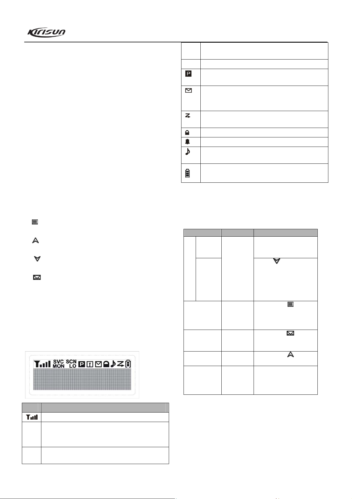
Chapter 2 External View and Functional
Keys
2.1 External View and Functional Keys
See Figure 2.1.
Figure 2.1
A. LED Indicator
Lights red while transmitting; lights green while receiving;
1
Page 3
PT6800 Service Manual
flashes red while in low battery power.
B. On/Off/Volume Control Knob
Rotate clockwise till a sound of click is produced to turn on
the radio; and rotate anticlockwise till a sound of click is
produced to turn off the radio. Rotate this knob to adjust the
volume while the radio is on.
C. Rotary Encoder
Rotate this knob to select your desired call address or
features for setting.
D. Antenna
E. Emergency Button
Press it to enable the “Emergency Call” function.
F. Clear Button
Press to return to Trunking Mode while in Conventional
Mode, or to end a call.
G. PTT (Push-To-Talk) Button
Press to call or transmit voice.
H. Redial/Monitor Button
Press to redial a number or monitor the channel.
I. “
” Key
Press to enter the Menu Mode.
J. “
” Key
Scroll upwards to view the previous page.
K. “ ” Key
Scroll downwards to view the next page.
L. “
” Key
Press to view status messages or data messages.
M. Numeric Keypad
Press to input the call address or dial a number.
N. Universal Connector
Connect to earphone or optional speaker/microphone.
2.2 Display Screen
Icon Description
Indicates the signal strength.
SVC
MON
Appears when a control channel is found. Flashes while
the radio is hunting for a control channel. (Trunking
Mode only)
Appears while you are monitoring a channel by pressing
the Monitor button. (Conventional Mode only)
SCN
Appears while you are scanning. (Conventional Mode
only)
Lo
Appears when the transmitting power is low.
Appears when you are in home system, and disappears
when in roaming. (Trunking Mode only)
Appears when there is new data received, including
voice message, digital data message and missed calls.
(Trunking Mode only)
Appears when you are in roaming. (Trunking Mode
only)
Appears when the keypad is locked.
Appears when the Rotary Encoder is locked.
Appears when the setting is not All Mute, and the ring
alert function is active.
Indicates the current battery power level, and flashes
when the battery power is low.
Chapter 3 Mode Introduction
3.1 Mode Introduction
Mode Function How to Enter
Trunking
Mode
User
Mode
Conventional
Mode
Panel Test Mode
Panel Tuning Mode
Version Information
Mode
PC Test Mode
3.2 Panel Test Mode
Please refer to Chapter 7 Adjustment.
3.3 Panel Tuning Mode
Please refer to Chapter 7 Adjustment.
3.4 PC Test Mode
2
For normal use.
Used by the
dealer to check
the fundamental
characteristics.
Used by the
dealer to tune the
radio.
Used to check
the version.
Used to tune the
radio by PC.
Press the Clear Button to return to
Trunking Mode while in
Conventional Mode.
Press “ ” key to enter
Conventional Mode while in
Trunking Mode. Or press the
combination keys set in PC
software to switch between the
two modes.
Press and hold “ ” key while
turning the radio power ON.
Press and hold “ ” key while
turning the radio power ON.
Press and hold “ ” key while
turning the radio power ON.
Run KSP6800 programming
software. Click “Program” in the
main menu, and then click “Test
Mode” in the pull-down menu.
Page 4
PT6800 Service Manual
Please refer to Chapter 7 Adjustment.
Chapter 4 Circuit Description
4.1 Preface
This portable radio is FM trunking portable equipment.
4.2 Frequency Configuration
Figure 4.1 Frequency Configuration
The receiver adopts double mixing. The first IF is
51.65MHz and the second IF is 450KHz.
The first local oscillator signal of the receiver is generated
by the frequency synthesizer. The second local oscillator signal
is generated by quadrupler X1.
The transmitter signal is directly produced by the frequency
synthesizer.
The reference frequency of the frequency synthesizer is
provided by TCXO.
4.3 Principle of Receiver (RX)
Figure 4.2 Principle of Receiver
Front End
The signal coming from the antenna passes through the
RX/TX switch circuit (D1, D39, D7, and D8), and passes
through a BPF consists of two LCs to remove unwanted
out-of-band signal, and then is routed to the low noise amplifier
(LNA) consists of Q18 and its peripheral components where it
is amplified.
Output signal from the LNA passes through a BPF consists
of three LCs to further remove unwanted out-of-band signal,
and then goes to the first mixer (Q19).
AGC Circuit
AGC circuit, which consists of Q17 and its peripheral
circuit, will work to reduce the gain of Q18 only when the input
signal is oversize.
First Mixer
The receiving signal from LNA is mixed with the first local
oscillator signal from the frequency synthesizer to produce the
first IF signal (51.65MHz).
IF Circuit
The first IF signal passes through crystal filter (XF1) to
remove the adjacent channel signal and signal outside the
adjacent channel. Then the filtered signal is amplified by the
first IF amplifier (Q20), and is routed to the IF processing IC
(IC4, TA31136).
IF IC consists of the second mixer, IF amplifier, limiter,
discriminator, noise amplifier, and audio low pass filter.
Signal (12.8MHz) from X1 is multiple-amplified by Q15
and its peripheral circuit to produce the second local oscillator
signal (51.2MHz). Then the second local oscillator signal
(51.2MHz) is mixed with the first IF signal (51.65MHz) in IC4
to generate the second IF (450KHz). And then the second IF
signal is amplified and limited in IC4, filtered in the ceramic
filter (CF1 or CF2, 450KHz), and demodulated in IC4. After
that, the demodulated signal is routed to the audio circuit to
output audio signal.
The selection circuit of the second IF filter consists of CF1,
CF2, D18, D19 and the peripheral circuit. When the radio is set
to wideband, CF2 is put through and takes effect, while CF1 is
cut off; when the radio is set to narrowband, CF1 is put through
and takes effect, while CF2 is cut off.
Squelch Circuit
The demodulated signal from IC4 is sent to the internal
noise amplifier in IC4. Then the resulting signal is further
amplified in Q21 and demodulated in D22, and then the
resulting DC level is routed to the MCU squelch control circuit.
This voltage is in inverse proportion to the input signal.
4.4 Principle of Transmitter (TX)
TX Power Amplification
3
Page 5
PT6800 Service Manual
Figure 4.3 Principle of Power Amplifier and Antenna Switch
The modulated RF signal from VCO is amplified in Q2, Q4,
Q59, Q5, and Q3, and is routed to Q1 for power amplification.
Grid bias of Q1 and Q3 is controlled by the APC circuit.
Through changing the grid bias voltage, the Tx output power
can be controlled conveniently.
APC (Automatic Power Control) Circuit
R57, R65, and R66 are used to test the power amplification
current. IC3A is the sampling amplifier for the power
amplification current. IC3B is the power comparator amplifier.
If the Tx output power is too high, the power amplification
current and IC3A output will increase; IC3B output voltage will
decrease, so the bias voltage of Q1 and Q3 will also decrease,
which causes the Tx output power to be lowered, and vice versa.
Thus the output power of Tx can keep stable under different
working conditions.
MCU can set the power through changing the voltage input
to IC3B.
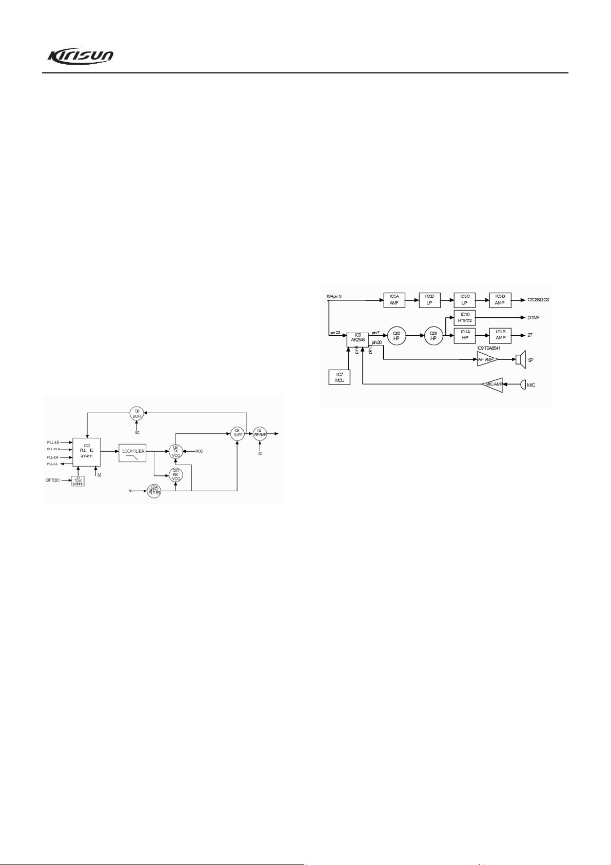
4.5 Principle of Frequency Synthesizer
The oscillation frequency from VCO goes to IC2 where it is
divided by the programmable divider and is then compared
with the reference frequency to obtain the error signal. The
signal is then filtered by a low pass filter, and is routed to VCO
to change the oscillation frequency of the VCO, enabling the
frequency to reach the set value. Then the VCO is locked.
Unlock detection: When PLL is unlocked, Pin 14 of IC2
will output the low level signal to MCU. Then MCU prohibits
the Tx from transmitting and makes an alert tone.
Q13 and other relevant circuits are used to switch the low
pass filters.
4.6 Audio Processing Circuit
Figure 4.4 Frequency Synthesizer
The radio adopts PLL type frequency synthesizer.
The frequency synthesizer consists of reference oscillator,
voltage control oscillator (VCO), programmable divider, phase
comparator, and low pass filter.
Tx VCO unit consists of Q6, D2, D4, D5, and D6. D9 is the
modulation circuit of Tx VCO.
Rx VCO unit consists of Q11, D11, D12, D13, and D14.
IC2 (ADF4111) is the PLL integrated circuit, which consists
of programmable reference divider, programmable divider,
phase comparator, and charge pump.
The low pass filter consists of R43 and C96.
The reference frequency is provided by X1 (TCXO,
12.8MHz).
The reference frequency from TCXO (Temperature
Controlled Crystal Oscillator) is divided by the programmable
reference divider in IC2 to produce reference frequency of
5KHz or 6.25KHz (determined by the preset channel frequency
and is controlled by MCU).
Figure 4.5 Audio Processing
IC6 (AK2346) is a special voice processing chip, which is
provided with functions of amplification, filtering,
pre-emphasis, de-emphasis, scrambling, companding, MSK
MODEM, etc. Most of the radio’s voice processing is done by
IC6.
MIC Signal Processing
The voice signal coming from the MIC passes through the
AGC circuit, and goes to IC24. One branch of the signal is
routed to IC24B (VOX circuit) for amplification, and then goes
to D35, where it is processed and turned into DC voltage, and
then sent to MCU for processing. The other branch of the signal
is routed to IC24A for amplification, and then goes to pin3 of
IC6, where it is amplified, filtered, companded (optional),
pre-emphasized, scrambled (optional), and limited, and then is
output from pin7 of IC6. After that, the resulting signal is sent
to VCO for modulation together with CTCSS/DCS. The 2T/5T
signal is input to pin6 of IC6. After being limited and amplified,
it is then output from pin7 of IC6, and is routed to VCO for
modulation.
RX Audio Signal Processing
Voice signal output from IC4 is divided into two parts. One
branch of the signal is routed to the low pass circuit consists of
IC5 and other components, where it is amplified and filtered (to
remove the voice signal) to obtain more purified CTCSS/DCS
4
Page 6

PT6800 Service Manual
signal, which is then sent to MCU for processing. The other
branch of the signal is routed to pin23 of IC6. After being
amplified and filtered, the signal is divided into two branches.
One branch (DTMF/2T/5T signals) is output from pin21 of IC6.
The DTMF/2T/5T signals passes through the high pass circuit
consists of Q30, Q31, and other components to remove the
subaudio signal. The DTMF signal goes to IC10 (HT9172
special DTMF decoding chip) to be decoded, and then is sent to
MCU for processing. The 2T/5T signal goes to IC1, where it is
filtered and reshaped, and then is routed to MCU for processing.
The other branch (voice signal) is scrambled, de-emphasized,
and companded, and is output from pin18 of IC6. Then the
resulting signal is input to pin19 of IC6. After being buffered
and amplified, it is then output from pin20 of IC6.
IC13 is a voice memory chip, which is stored with voices of
channel indication etc. Once the rotary encoder is switched, the
speaker will announce the current channel number. User can
press the preprogrammed “Voice Alert” key to repeat the
current channel number.
After the RX audio signal, voice alert signal, 2T/5T/DTMF
signal, alert tone signal, and emergency alarm signal join
together, they are amplified by audio power amplification IC9,
and then drive the speaker.
Impedance of the speaker: 16
Note:
* None of the terminals of the speaker should be grounded.
* The emergency alarm sound has no volume limit.
4.7 Power Supply
The radio adopts 7.2V battery as power supply. The Tx
power amplification circuit (Q1 and Q3) and the Rx audio
power amplifier (IC9) directly adopts the battery as power
supply. Power of other circuits is supplied by the regulated
voltage (5V).
Q40 and Q45: 5V low dropout, micro-power regulator.
Q43: 5T switch, controlled by MCU.
5T: Supplies power for front end of Tx.
Q39: 5R switch, controlled by MCU.
5R: Supplies power for RF amplifier, mixer, IF processing
unit, and audio signal processing unit etc. of Rx.
Q44: 5C switch, controlled by MCU.
5C: 5V power supply under SAVE control. Supplies power
for frequency synthesizer.
4.8 MCU Unit
MCU unit controls the operation of each unit of the radio so
that all functions can be realized.
Communicate with external PC.
Access the status data of the radio.
Control the PLL to generate Rx and Tx local oscillator
frequencies.
Obtain status parameters of current channel.
Control status of LED indicator.
Control power supply for each unit.
Check the actions of each functional key.
Generate CTCSS signal.
Generate DCS signal.
Generate power control signal.
Perform CTCSS decoding.
Perform DCS decoding.
Test and control the squelch.
Control content of voice alert.
Memory (E
2
PROM, A T24C256):
The memory is stored with channel data, CTCSS/DCS data,
other data for function setting, and parameter adjusting data of
the radio.
CTCSS/DCS Signal Encoding and Decoding
The CTCSS/DCS signal (output from pin24 and pin28,
PWM wave) generated by MCU is routed to VCO and TCXO
respectively for modulation.
The CTCSS/DCS signal from the receiver is decoded by
MCU. MCU checks if the CTCSS/DCS signal in the receiving
signal matches the preset CTCSS/DCS of the radio, and
determines whether to open the speaker or not.
CTCSS Signal
CTCSS (Continuous Tone Control Squelch System) is a
squelch control system which is modulated on carrier and is
guided by a continuous subaudio signal. If CTCSS is set, the
communication between the transmitting and receiving radios
can be realized only when the two radios has set the same
CTCSS. In doing this, disturbance from other signals can be
avoided.
PT6800 has 39 groups of standard CTCSS frequencies for
your selection. See table 4.1.
CTCSS signal is generated by MCU (PWM waveform), and
is passed through low pass filter consists of RC to remove high
frequency component (above 300Hz). Then the resulting signal
is routed to VCO for modulation.
Table 4.1 CTCSS Frequencies
5
Page 7
PT6800 Service Manual
No. Frequency
1 67.0 11 94.8 21 131.8 31 186.2
2 69.3 12 97.4 22 136.5 32 192.8
3 71.9 13 100.0 23 141.3 33 203.5
4 74.4 14 103.5 24 146.2 34 210.7
5 77.0 15 107.2 25 151.4 35 218.1
6 79.7 16 110.9 26 156.7 36 225.7
7 82.5 17 114.8 27 162.2 37 233.6
8 85.4 18 118.8 28 167.9 38 241.8
9 88.5 19 123.0 29 173.8 39 250.3
10 91.5 20 127.3 30 179.9
DCS Signal
DCS (Digital Code Squelch), which is used to control the
squelch, is a series of continuous digital codes modulated on
carrier together with voice signal. If DCS is set, the speaker can
be opened only when the radio receives signal with the same
DCS, so disturbance of unwanted signals can be avoided.
PT6800 has 83 standard codes (inverted and non-inverted)
for your selection. See table 4.2.
DCS signal is generated by MCU (PWM waveform). It
passes through the low pass filter consists of RC to remove the
high frequency components (above 300Hz). Then the resulting
signal is routed to VCO and TCXO for modulation, with HF
components of the DCS signal being modulated by VCO, and
the LF components of the DCS signal being modulated by
TCXO.
The DCS signal coming from the receiver is routed MCU
for decoding. MCU checks if the DCS code in the received
signal matches the preset DCS of the radio, and determines
whether to open the speaker or not.
Table 4.2 DCS codes
023 114 174 315 445 631
025 115 205 331 464 632
026 116 223 343 465 654
031 125 226 346 466 662
032 131 243 351 503 664
043 132 244 364 506 703
047 134 245 365 516 712
051 143 251 371 532 723
054 152 261 411 546 731
065 155 263 412 565 732
071 156 265 413 606 734
072 162 271 423 612 743
[Hz]
No. Frequency
[Hz]
No. Frequency
[Hz]
No. Frequency
[Hz]
073 165 306 431 624 754
074 172 311 432 627
4.9 Semiconductor Data
MCU Description
Table 4.3 Description for Ports of Microprocessor (M30620)
No. I/O Port Name Function
1 O VCCN PLL reference frequency adjust
2 O TONEO 2T/5T/DTMF/BEEP signal output
3 I TONEI 2T/5T signal input
4 O E-SDA E2PROM data line
5 O E-SCL E2PROM clock line
6 - C-BYTE GND
7 - C-CNVSS GND
8 O SHIFT Clock beat shift H: Clock beat shift
9 O E-TEST E2PROM write protect pin H: Not writable L: Writable
10 I RESET Reset pin
11 O XOUT Clock output pin
12 - VSS GND
13 I XIN Clock input pin
14 - VCC 5V power supply
15 - CMMI GND
16 I INTO Power down detect pin
17 O A-RDT AK2346 control pin
18 O A-TCLK AK2346 control pin
19 O A-SCLK AK2346 control pin
20 O A-DI/O AK2346 control pin
21 O A-TDATA AK2346 control pin
22 O A-DIR AK2346 control pin
23 - NC -
24 O CTCSS VCO CTCSS/DCS output pin (to VCO for modulation)
25 O PLL-LP
26 O PC/TV Power control or Rx pass band tuning voltage control
27 - NC -
28 O
29 O C-TXD1 Serial data output, communicate with PC
30 O C-RXD1 Serial data input, communicate with PC
31 - C-CLK1 GND
32 - NC -
33 - ICA -
34 O PABC Power control for final power amplifier H: Transmitting
35 O APC2 SW Power amplifier control switch H: Transmitting
36 O APC1 SW Power amplifier control switch L: Transmitting
37 O RX SW Rx VCO power switch L: Receiving
38 O TX SW Tx VCO power switch L: Transmitting
39 - C-HOLD GND
40 I PLL-UL PLL unlock detect pin
41 O PLL-STB PLL enable pin
42 O PLL-DATA PLL data pin
43 O PLL-CLK PLL clock pin
44 - C-VCC Connect to power supply
45 O
46 O GREEN Green LED H: ON
47 O RED Red LED H: ON
48 O 5TC 5T control switch L: 5T is 5V
49 O 5RC 5R control switch L: 5R is 5V
50 O 5CC Battery save control switch L: 5C is 5V
51 O W/N N Wideband/Narrowband-Narrowband H: Narrowband
52 O W/N W Wideband/Narrowband-Wideband H: Wideband
53 O AFCO AF power amplifier control H: Amplifier works
54 O RX MUTE Rx mute control L: Mute
55 I W-BUSY Voice announcing chip busy signal detect H: Busy
CTCSS
MAX AF
PLL - low pass filter toggle switch
H: Switch above center frequency point
CTCSS/DCS output pin (to TCXO for modulation)
TCXO
Max. volume control L: Max. volume
SW
6
Page 8
PT6800 Service Manual
56 O W-DATA Voice announcing data signal
57 O W-SCLK Voice announcing clock signal
58 O W-MUTE Voice announcing mute control L: Mute
59 O S-SCK -
60 - ACC 5V power supply
61 O S-SI -
62 - VSS GND
63 O S-SO -
64 O S-CS -
65 - - -
66 I PTT PTT key input L: Transmitting
67 I H-D3 DTMF data input
68 I H-D2 DTMF data input
69 I H-D1 DTMF data input
70 I H-D0 DTMF data input
71 I H-DV DTMF data input
72 I DN Encoder switch signal
73 I UP Encoder switch signal
74 O L-AO LCD control signal
75 O L-AO LCD control signal
76 O L-AO LCD control signal
77 O L-AO LCD control signal
78 O L-AO LCD control signal
79 I/O K1 Keyboard signal
80 I/O K1 Keyboard signal
81 I/O K1 Keyboard signal
82 I/O K1 Keyboard signal
83 I/O K1 Keyboard signal
84 I/O K1 Keyboard signal
85 I/O K1 Keyboard signal
86 I/O K1 Keyboard signal
87 O LAMP Backlight control signal H: ON
88 I BATT Battery voltage detect
89 I RSSI Received signal strength indication detect
90 I BUSY Noise level detect
91 I VOX Voice control level detect
CTCSS/DCS
92 I
93 I PF Programmable button input
94 - AVSS GND
95 I MANDOWN MANDOWN signal input L: Valid
96 - VREF Connect to power supply
97 - AVCC Connect to power supply
98 O VOX SW VOX power control L: VOX enabled H: VOX disabled
99 O MIC MUTE MIC mute switch L: Mute
100 O HPF PC
Table 4.4 Function Description of Semiconductor Components
Position
Mark
IC11 PST9140NR MCU reset circuit
IC14 TC75W51FU MIC amplification, limitation, and filtering
IC2 ADF4111 Frequency synthesizer
IC3 NJM2904 APC, voltage comparison, driving
IC4 TA31136
IC5 NJM2902
IC6 AK2346 Audio processing chip
IC7 M30620 MCU
IC8 AT24C256
IC9 TDA8541 Rx audio power amplifier
RD07L RQA0002 Tx final power amplifier
CTCSS/DCS signal input
IN
High pass power control L: Scramble enabled H:
Scramble disabled
Model Function Description
Rx second local oscillator, second IF
amplification, limitation, demodulation, and
noise amplification
Rx demodulation signal amplification and
filtering
E2PROM, stores channel frequency data,
function setting parameters, and adjusting status
parameters
Q10 DTC144EUA APC control switch
Q11 2SK508NV Rx VCO oscillator circuit
Q12 DTA144EE APC output switch
Q12 DTA144EE APC control switch
Q13 2SC4116 PLL low pass switch
Q14 2SC4617 VCO power supply filter
Q15 2SC5108 Rx second oscillator frequency multiplier circuit
Q16 DTC144EE APC control switch
Q17 2SK1829 Rx high power amplifier gain control switch
Q18 3SK318 Rx high power amplifier
Q19 3SK318 First mixer
Q2 2SC5108 VCO buffer amplifier
Q20 2SC5108 First IF amplifier
Q21 2SC4617 Rx noise amplifier
Q22 DTC144EE Red LED drive
Q23 DTC144EE Wideband-Narrowband noise toggle switch
Q24 DTC144EE Green LED drive
Q25 DTA144EE
Wideband-Narrowband discriminator toggle
switch
Q26 DTA123JE 2T high pass filter control switch
Q29 2SK1824 2T high pass filter control switch
Q3 RD01MUS1 Tx power amplifier drive
Q30 2SC4617 2T high pass filter circuit
Q31 2SC4617 2T high pass filter circuit
Q32 DTC144EE Beat control switch
Q33 2SK1824 Rx audio mute switch
Q34 2SK1824
Rx audio output switch, disconnect when
emergency alarm ON.
Q35 DTC144EE Audio power amplifier control switch
Q36 DTA144EE MIC amplification unit power switch
Q37 2SK1824 Voice alert switch
Q38 2SA1586 External PTT detect switch
Q39 ST2301 5R switch
Q4 2SC5108 VCO buffer amplifier
Q40 XC6024B502MR 5V regulated voltage output
Q41 2SC4116 MIC AGC control switch
Q42 DTC144EE External PTT detect switch
Q43 ST2301 5T switch
Q44 DTA123JE 5C switch
Q45 XC6024B502MR 5V regulated voltage output
Q47 2SA1586 MIC AGC control switch
Q48 ST2302 External speaker control switch
Q49 2SC5108 Tx first amplifier
Q5 2SC3356 Tx second amplifier
Q51 2SK1824
Rx audio output switch, connect when
emergency alarm ON.
Q6 2SK508NV Tx VCO oscillator circuit
Q7 DTA143TE Tx VCO control switch
Q8 2SC5108 VCO buffer amplifier
Q9 DTA143TE Rx VCO control switch
Table 4.5 Function Description of Diodes
Position
Mark
D1 HVC131 Tx antenna switch diode
D10 MA2S111
D11 HVC376
D12 HVC376 Rx VCO oscillation varactor diode
D13 HVC376 Rx VCO oscillation varactor diode
D14 HVC376
D15 HZU5ALL APC output voltage limiting diode
D16 MA2S111 VCO power filtering acceleration diode
D17 HSC277 VCO output switch
D18 DAN222
D19 DAN222
Model Function Description
Unlock detect diode
Rx VCO oscillation varactor diode
Rx VCO oscillation varactor diode
Rx second IF filter wideband-narrowband toggle
switch
Rx second IF filter wideband-narrowband toggle
switch
7
Page 9
PT6800 Service Manual
D2 HVC376
D21 HVC355B
D22 MA742
D23 HVC355B
D26 LED green
D27 HVC376B Rx bandpass filter varactor diode
D28 LED red
D28 HVC376B Rx bandpass filter varactor diode
D29 HVC376B Rx bandpass filter varactor diode
D3 HSC277 VCO output switch
D30 HVC376B Rx bandpass filter varactor diode
D31 LED green Receiving indication
D35 MA742 VOX detect diode
D36 MA742 MIC AGC detect diode
D37 MA742 MIC AGC detect diode
D39 HVC131 Tx antenna switch diode
D4 HVC376 Tx VCO oscillation varactor diode
D40 HVC376B Rx bandpass filter varactor diode
D5 HVC376 Tx VCO oscillation varactor diode
D6 HVC376 Tx VCO oscillation varactor diode
D7 HSC277 Antenna toggle switch
D9 1SV278 Tx VCO modulation diode
Table 4.6 Features of Crystal Filter XF1
Item Rated Value
Nominal center frequency 51.65MHz
Pass bandwidth ±7.5kHz or higher
40dB stop bandwidth ±20.0kHz or lower
Pulse 1.0dB or lower
Insertion loss 3.0dB or lower
Guarantee attenuation 80dB or higher
Terminal impedance 330
Table 4.7 Performances and Features of CF1 LTWC450H
Item Rated Value
Nominal center frequency 450kHz
6dB bandwidth ±3.0kHz or higher
50dB bandwidth ±9.5kHz or lower
Pulse 2.0dB or lower
Insertion loss 6.0dB or lower
Guarantee attenuation 47.0dB or higher
Terminal impedance 1.5k
Table 4.8 Performances and Features of CF1 LTWC450F
Item Rated Value
Nominal center frequency 450kHz
6dB bandwidth ±6.0kHz or higher
50dB bandwidth ±12.5kHz or lower
Pulse 2.0dB or lower
Insertion loss 6.0dB or lower
Guarantee attenuation 47.0dB or higher
Terminal impedance 1.5k
Tx VCO oscillation varactor diode
Rx bandpass filter varactor diode
Noise demodulation
Rx bandpass filter varactor diode
Receiving indication
Transmitting indication
Chapter 5 Function Description and
Parameter Setting
5.1 Characteristics
1) The radio conforms to the MPT1327 signaling protocol
standard, applies to a variety of base station systems including:
Tait, TaiHe, WanGe, QiaoHang etc., and supports various call
methods.
2) The radio conforms to the MPT1343 standard.
3) The radio is provided with special functions of remote killing,
reactivating, and dynamic grouping.
4) 32 conventional channels, standard CTCSS/DCS signaling,
BCL, TOT, and scan function.
5) 16 test frequencies and parameter indications, which are
convenient for the dealer to test the radio.
6) Power, deviation, sensitivity and other parameters are
programmed at the factory.
5.2 Trunked Features
1) Trunking signaling
The radio conforms to MPT1327 trunking signaling and
MPT1343 standard.
2) Hunt
64 control channels can be programmed for the radio, and
the radio will hunt for a control channel automatically.
3) Trunking calls
The following calls can be performed by the radio:
inter-prefix individual call, inter-prefix group call, inter-fleet
individual call, inter-fleet group call, voice call, status message
call, short data message call, conference call, broadcast call,
priority call, emergency call, PABX call, PSTN call, NPD
transfer, own call diversion, third party call diversion, include
call, ALLI call, network operator service call, technician call,
don’t disturb facility, queue incoming call, etc.
4) Emergency call
Press the orange “Emergency Button” to send an emergency
call in case of emergency.
5) Dynamic grouping
Dynamic grouping function allows the base station to group
units as a new team by remote control.
6) Remote killing
The base station can give remote killing order to the lost or
stolen radio to prohibit its operation.
7) Reactivating
The base station can give reactivating order to the remote
killed radio so that it can return to normal operation.
8) Missed calls
Missed calls can be displayed, and the status of the missed
calls can be stored.
9) Contact list
Large memory of 200 contacts.
10) Status message
8
Page 10
PT6800 Service Manual
Content of status messages can be programmed by PC
software. Alert tone sounds while messages are received, and
the status message can be checked by the user.
11) Redialing
10 groups of dialed number can be stored in the radio. Press
the Redial Button, the dialed number can be displayed on LCD,
select the number you want and press PTT or “#” key to call.
12) Don’t disturb
This function allows the radio to refuse voice calls, status
message calls, and short data calls.
5.3 Conventional Features
1) CTCSS/DCS
The dealer may have set CTCSS/DCS on channels of the
radio. In doing this, other irrelevant calls using the same
channel can be ignored. If a channel has set CTCSS/DCS, the
squelch can be opened only when the received signal has the
same CTCSS/DCS.
2) DTMF dialing
Input the number while pressing the PTT key. Then you can
hear DTMF sound from the speaker.
3) Busy channel lockout (BCL)
This function can prevent other radios on the same channel
from being interfered. When the channel is occupied, the radio
will prohibit transmitting signals.
4) Time-Out Timer (TOT, TOT pre-alarm, TOT-rekey, TOT
reset)
TOT is used to prevent any person from using a channel to
transmit for an extended period of time. If the continuous
transmission time is longer than the preset time limit, the radio
will make alarm tone and stop transmitting.
5) Channel scan
32 conventional channels can be set through PC
programming software, and the parameters on each channel can
be set, such as CTCSS/DCS encoding and decoding,
wideband/narrowband, BCL, high power/low power,
compander, channel name, etc. If signals are detected while in
channel scanning, the scanning will pause and the information
of the paused channel will be displayed.
5.4 General Features
1) Channel spacing
The channel spacing can be selected (12.5kHz/25kHz)
through PC programming software.
2) Signal strength display
The real time signal strength can be displayed on the screen.
3) Battery power display and low battery warning
The battery power can be displayed on the screen and when
the battery power is low, the battery indicator will flash to
warn.
5.5 Functional Parameter Setting
The radio’s functional parameters have been set before
leaving the factory. However, due to different requirements of
users, the radio’s trunked features, operating frequency,
channels, CTCSS/DCS, scan, and other function parameters
should be reset. Therefore, the company has specially designed
a set of Chinese/English programming software KSP6800 with
friendly interface, convenient operation and visualized display
for setting functional parameters of the radio.
Steps for setting the functional parameters of the radio by
computer are as follows:
A. Install KSP6800 on the computer.
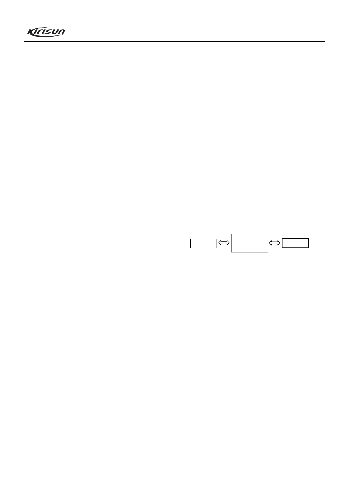
B. Connect the radio to the COM port of the computer with
the special programming cable. Refer to the figure below.
Note: While connecting, make sure that the power of the
computer and the radio are both turned off.
Computer
Programming cable
for PT6800
Radio
C. Turn the computer power ON.
D. Turn the radio power ON.
E. Run the KSP6800 programming software by double
clicking its executive program.
F. Click “Program” in the main menu of KSP6800, and
click “Read from radio” in the pull-down menu to read
parameters of the radio to the computer; click “Write to radio”
in the pull-down menu to write parameters in the computer to
the radio.
G. The following parameters can be set by using KSP6800
according to requirements of the user:
1) Basic parameters of the system
2) System code
3) Channel parameters
4) Frequencies
5) Hunt option of control channel
6) Personalization
7) Call facilities
8) Call scope limit
9) Call address
10) Default call address
11) Contact list and relevant options
12) 5 digit dialed string
9
Page 11

PT6800 Service Manual
13) Security feature
14) Function menu
15) Trunked features
16) Conventional features
17) Conventional channels
18) Power ON message
Please refer to the “Help” document of KSP6800 and
Instruction Manual of PT6800 for details.
Chapter 6 Disassembly for Repair
The radio is a kind of sophisticated communication
equipment with precise structure and small size. You should
disassemble it carefully during the maintenance. The
instructions for the disassembly are as follows.
6.1 Installing/Removing the Battery
6.1.1 Installing the battery
1) Insert the three bulges at the lower end of the battery into the
holes at the lower end of the shell of the radio.
2) Press down the battery to lock it in place until a click is
heard. (See Figure 6.1)
Figure 6.1
6.1.2 Removing the battery
Use your thumb to press the belt clip, and one side of your
index finger to press the release button (See Figure 6.2), the
battery will bounce out automatically. And then pull the battery
away from the radio.
Figure 6.3
6.3 Installing/Removing the Belt Clip
Slide the guide rails on the belt clip along the grooves on
the rear of the battery until the belt clip is hooked. When
removing the belt clip, lift the sheet metal on the top of the belt
clip with your finger nail or a tool while pushing the belt clip
upward. (Refer to Figure 6.4)
Figure 6.4
6.4 Removing the Front Cabinet from the Chassis
1) Pull out the knobs and screw off the antenna;
2) Remove the two nuts of the knobs and nut of the antenna
with a special tool;
3) Remove the two fixing screws at the lower part of the Al
chassis by a hexagonal screwdriver;
4) Insert a flat-blade screwdriver into the slot at the lower part
of the Al chassis, and prize up it. Then pull the chassis to
remove it from the front cabinet.
5) Take off the flat cable connecting the main PCB and the key
board PCB from the main PCB.
See Figure 6.5.
Figure 6.2
6.2 Installing the Antenna
Hold the bottom of the antenna and turn it (clockwise) into
the connector on the top of the radio until secure. See Figure
6.3.
Figure 6.5
6.5 Removing the Main Board from the Al Chassis
1) Remove the top waterproof material;
2) Remove the screw on the PTT board, and then take off the
PTT board;
10
Page 12
PT6800 Service Manual
3) Remove the screws on the PCB;
4) Remove the solder of the antenna terminal with a soldering
iron. Then take off the main board.
See Figure 6.6.
Figure 6.6
6.6 Removing the Key Board from the Front Cabinet
Remove the screws on the key board, and then you can
separate the key board from the front cabinet. (Refer to Figure
6.7)
Figure 6.7
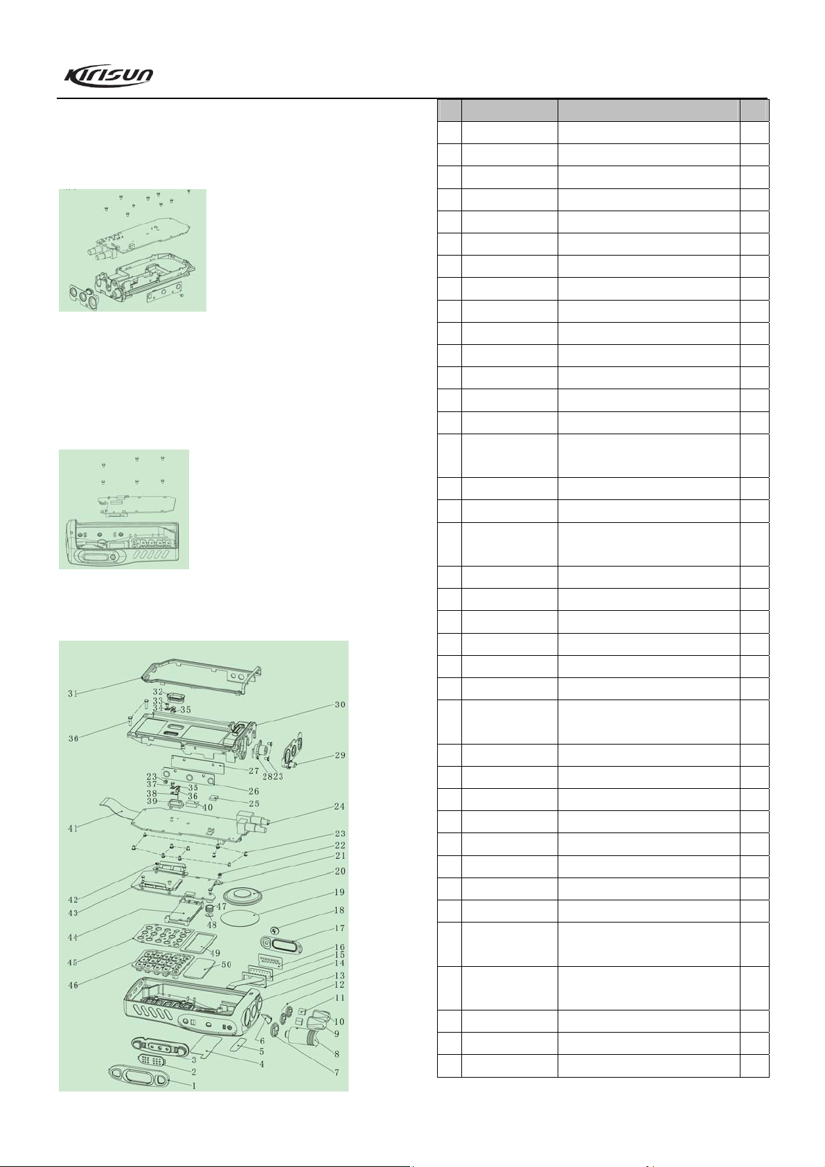
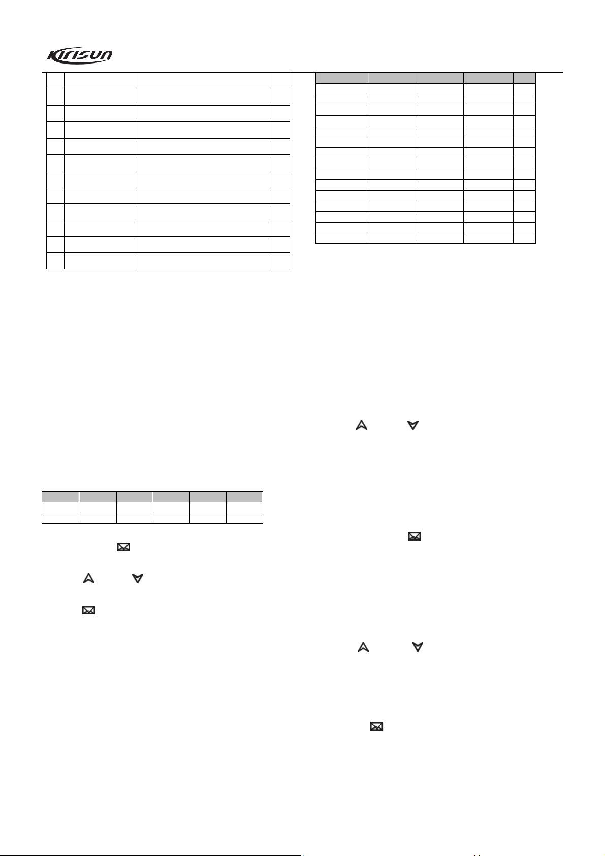
6.7 Exploded View
No. Part No. Description PCS
1 201-006500-R02 PTT Cover 1
2 201-006500-R05 PTT Key 1
3 202-006500-R01 Rubber PTT Key 1
4 204-006800-R01 LCD Protective Film 1
5 LOGO 1
6 201-006500-R09 Light Guide 1
7 203-000558-R11 Nut for Antenna 1
8 Antenna 1
9 201-006500-R04 Rotary Encoder 1
10 201-006500-R03 Volume Knob 1
11 203-006800-R26 Circlip for Knob 2
12 305-108020-R01 Nut for Knob 2
13 201-006500-R01 Front Cabinet 1
14 204-007200-R02 Tape for Universal Connector PCB 1
15
16 204-006500-R03 Tape for Universal Connector 1
17 204-006800-R22 Universal Connector Cover 1
18 304-30030G-R02
19 204-003208-R02 Waterproof Net for Speaker 1
20 121-100000-R17 Speaker 1
21 Keypad PCB 1
22 302-20060G-R01 Self-tapping Screw ST2.0*6.0 1
23 301-20040G-R01 Machine Screw M2.0*4.0 13
24 Main PCB 1
25 202-003208-R07
26 203-006500-R06 Metal Dome for PTT Key 1
27 PTT Key PCB 1
28 203-000558-R07 Antenna Connector 1
29 202-006500-R03 Top Waterproof 1
30 203-006500-R01 Al Chassis 1
31 202-006500-R02 Main Waterproof 1
32 202-006500-R05 Waterproof for Anode Bracket 1
33 301-20030G-R01 Machine Screw M2.0*3.0 1
34 203-006500-R04
35 202-000558-R08
36 301-20080G-R02 Machine Screw M2.0*8.0 2
37 302-17040G-R01 Self-tapping Screw ST1.7*4.0 1
38 203-006500-R02 Anode Connecting Sheet 1
11
Universal Connector PCB &
FPCB
Screw for Universal Connector
Cover
Heat-conductive Silicone Rubber
Washe r
Battery Contact Sheet
(Anode/Cathode)
Rubber Washer for Battery Contact
Sheet
1
1
1
2
2
Page 13
PT6800 Service Manual
39 201-006500-R06 Anode Bracket 1
40 204-006200-R04 Sponge Cushion 1
41 120-400000-R13 Flat Cable 1
42 301-20020G-R01 Machine Screw M2.0*2.0 4
43 203-006500-R07 Grounded Sheet 2
44 102-6800CN-R01 LCD Display Module 1
45 203-006500-R03 Keypad Metal Dome 1
46 202-006500-R06 Numeric Keypad 1
47 202-000558-R09 Waterproof MIC Cover 1
48 204-006800-R06 MIC Washer 1
49 204-006500-R01 Dustproof Washer for LCD Lens 1
50 201-006500-R08 LCD Lens 1
Chapter 7 Adjustment
7.1 Adjustment Method
After changing components during the maintenance, it is
necessary to test the radio and adjust its technical parameters.
7.1.1 Components required during adjustment
1) Antenna connector converter
2) Universal connector
7.1.2 Manual tuning method
1) Five frequency points of the radio need to be adjusted.
The following table is the frequencies corresponding to the
numeric keys.
Radio Model Key 1 Key 2 Key 3 Key 4 Key 5
PT6800 (2) 350.05MHz 370.05MHz 389.95MHz 360.05MHz 380.05MHz
PT6800 (4) 400.05MHz 435.05MHz 469.95MHz 417.05MHz 452.05MHz
2) Panel tuning mode (Manual)
Press and hold “
to enter the panel tuning mode.
Press “
” key or “ ” key to select the item you want to
adjust.
Press “
” key to save the adjusted parameters.
Press the “Redial Button” to switch between wideband and
narrowband.
Press key “7” to switch between “Emphasis” and
“De-emphasis”.
Press key “8” to enable or disable “Compander” function.
Press key “9” to enable or disable “Beat Shift” function.
Turn the rotary encoder to adjust the parameters of the radio.
Press key “1”, “2”, “3”, “4”, and “5” to choose the five
frequency points of the radio.
Items need to be adjusted and the tuning points under tuning
mode are listed in the following table:
” key while turning the radio power ON
Item Display Tuning Method Tuning Point Tx/Rx
Frequency FREQUENCY Rotary Encoder Center freq point Tx
High power HIGH POWER Rotary Encoder Five freq points Tx
Low power LOW POWER Rotar y Encoder Five freq points Tx
DQT balance DQT BALANCE Rotary Encoder Five freq points Tx
Max deviation MAX DEV Rotary Encoder Five freq points Tx
QT deviation QT DEV Rotary Encoder Five freq points Tx
DQT deviation DQT DEV Rotary Encoder Five freq points Tx
DTMF deviation DTMF DEV Rotary Encoder Center freq point Tx
FFSK deviation FFSK DEV Rotary Encoder Center freq point Tx
Tone deviation TONE DEV Rotary Encoder Center freq point Tx
Battery detect BATT Rotary Encoder Center freq point Tx
Sensitivity SENS Rotary Encoder Five freq points Rx
Squelch SQL Rotary Encoder Five freq points Rx
RSSI (low) LOW RSSI Rotary Encoder Five freq points Rx
RSSI (high) HIGH RSSI Rotary Encoder Five freq points Rx
3) Parameter adjustment
Rx Part
Set the general test set and the radio, and make sure that the
test set is in its Rx interface, and the radio is in the Tuning
Mode.
1. Sensitivity: SENS
a) Set the signal strength of the general test set to be -119dBm
(wideband/narrowband), set its modulation signal to be 1kHz,
and the deviation to be ±3kHz (wideband), ±1.5kHz
(narrowband). Set the filter of the general test set to be in the
bandpass status.
b) Press “
” key or “ ” key to select SENS in the radio.
Then turn the volume knob of the radio to make the output
audio power indicated in the general test set to be 500mW.
Then adjust the five frequency points.
c) Press key “1”, “2”, “3”, “4”, “5” respectively (corresponding
to the five frequency points of the radio), turn the rotary
encoder to make the SINAD indicated in the general test set to
be 12dB. Then press “
” key to save.
2. Squelch: SQL CLOSE, SQL OPEN
a) Set the signal strength of the general test set to be -121dBm
(SQL OPEN)/-123dBm (SQL CLOSE), set its modulation
signal to be 1kHz, and the deviation to be ±3kHz (wideband),
±1.5kHz (narrowband). Set the filter of the general test set to be
in the bandpass status.
b) Press “
” key or “ ” key to select SQL OPEN/SQL
CLOSE in the radio. Then turn the volume knob of the radio to
make the output audio power indicated in the general test set to
be 500mW.
c) Turn the rotary encoder. When the value displayed keeps
stable, press “
” key to save. (Press key “1”, “2”, “3”, “4”,
“5” respectively to adjust the five frequency points of “Low”,
“Lower”, “Mid”, “Higher”, and “High”)
Note: Press the “Redial Button” to switch between
wideband and narrowband.
12
Page 14

PT6800 Service Manual
3. RSSI: LOW RSSI/HIGH RSSI
a) Set the signal strength of the general test set to be -120dBm
(LOW RSSI)/-70dBm (HIGH RSSI), set the modulation signal
of the audio signal generator to be 1kHz, and the deviation to
be ±3kHz (wideband), ±1.5kHz (narrowband). Set the filter of
the general test set to be in the bandpass status.
b) Press “
turn the volume knob of the radio to make the output audio
power indicated in the general test set to be 500mW.
c) After the signal source transmit the signal, turn the rotary
encoder of the radio, and then press “
key “1”, “2”, “3”, “4”, “5” respectively to adjust the five
frequency points of “Low”, “Lower”, “Mid”, “Higher”, and
“High”)
Note: Press the “Redial Button” to switch between
wideband and narrowband.
Tx Part
Set the general test set and the radio, and make sure that the
test set is in its Tx interface, and the radio is in the Tuning
Mode.
1. Tx frequency: FREQUENCY
a) Press “
radio.
b) Turn the rotary encoder to make the Tx frequency to be
within ±100Hz.
2. Tx power: HIGH POWER/LOW POWER
a) Press “
POWER in the radio.
b) Turn the rotary encoder to make the Tx power to be
3.5~5.0W (HIGH POWER)/0.3~0.7W (LOW POWER). (Press
key “1”, “2”, “3”, “4”, “5” respectively to adjust the Tx power
of the five frequency points.)
3. Max. deviation: MAX DEV
a) Set the modulation signal of the general test set to be
1kHz/320mV. And set the filter to be in the low pass status.
b) Press “
radio.
c) Turn the rotary encoder to make the max. deviation to be
1.8-2.5kHz (narrowband)/3.8-4.8kHz (wideband). (Press key
“1”, “2”, “3”, “4”, “5” respectively to adjust the max. deviation
of the five frequency points of “Low”, “Lower”, “Mid”,
“Higher”, and “High”)(Pre-emphasis is disabled, and no SVC is
displayed.)
Note: Press the “Redial Button” to switch between
wideband and narrowband.
” key or “ ” key to select RSSI in the radio. Then
” key to save. (Press
” key or “ ” key to select FREQUENCY in the
” key or “ ” key to select HIGH POWER/LOW
” key or “ ” key to select MAX DEV in the
4. DQT balance: DQT BALANCE
a) Set the filter to be in the low pass status.
b) Press “
radio.
c) Turn the rotary encoder to make the waveform of DQT to be
flat square wave. (Press key “1”, “2”, “3”, “4”, “5” respectively
to adjust the DQT balance of the five frequency points of
“Low”, “Lower”, “Mid”, “Higher”, and “High”)
5. QT/DQT deviation: QT DEV/DQT DEV
a) Set the filter to be in the low pass status.
b) Press “
radio.
c) Turn the rotary encoder to make the QT/DQT deviation to be
0.3-0.5kHz (narrowband)/0.5-0.85kHz (wideband). (Press key
“1”, “2”, “3”, “4”, “5” respectively to adjust the QT/DQT
deviation of the five frequency points of “Low”, “Lower”,
“Mid”, “Higher”, and “High”)
Note: Press the “Redial Button” to switch between
wideband and narrowband.
6. FFSK deviation: FFSK DEV
a) Set the filter to be in the band pass status.
b) Press “
radio.
c) Turn the rotary encoder to make the FFSK deviation to be
1.5kHz (narrowband)/3.4kHz (wideband).
Note: Press the “Redial Button” to switch between
wideband and narrowband. Only the center frequency point
needs to be adjusted.
7. DTMF deviation: DTMF DEV
a) Set the filter to be in the band pass status.
b) Press “
radio.
c) Turn the rotary encoder to make the DTMF deviation to be
1.5kHz (narrowband)/3.4kHz (wideband).
Note: Press the “Redial Button” to switch between
wideband and narrowband. Only the center frequency point
needs to be adjusted.
8. Tone deviation: TONE DEV
a) Set the filter to be in the band pass status.
b) Press “
radio.
c) Turn the rotary encoder to make the tone deviation to be
1.5kHz (narrowband)/3.4kHz (wideband).
Note: Press the “Redial Button” to switch between
wideband and narrowband. Only the center frequency point
needs to be adjusted.
13
” key or “ ” key to select DQT BALANCE in the
” key or “ ” key to select QT/DQT DEV in the
” key or “ ” key to select FFSK DEV in the
” key or “ ” key to select DTMF DEV in the
” key or “ ” key to select TONE DEV in the
Page 15

PT6800 Service Manual
9. Battery detect: BATT
Set the voltage of the power supply to be 6.8V. Press “
key or “
value keeps stable, press “ ” key to save the data.
Note: After the above mentioned items are adjusted to the
target value, you need to press “
7.1.3 PC test mode
1. VCO
In the receiving status:
a) Set the Rx frequency to the high frequency point, and tune
C117 to make the voltage of T1 to be 3.6 ± 0.1V.
b) Set the Rx frequency to the low frequency point, and make
the voltage of T1 to be >0.6V.
In the transmitting status:
c) Set the Tx frequency to the high frequency point, and tune
C52 to make the voltage of T1 to be 3.6 ± 0.1V.
d) Set the Tx frequency to the low frequency point, and make
the voltage of T1 to be >0.6V.
Run the PT 6800 programming software. Click
“Program” in the main menu, and click “Test Mode” in
the pull-down menu. Then the PC tuning interface will pop up.
The adjusting items will be listed on the left of the interface.
Double click the item you want to adjust, and then the
following parameters can be tuned.
2. Tx part
1) Tx frequency
Tune the value of “Frequency Stability” to adjust the Tx
frequency to be within nominal frequency ± 100Hz.
2) Power
a) Tune the value of “High Power” (five frequency points) to
make the Tx high power to be 3.5-5.0W.
b) Tune the value of “Low Power” (five frequency points) to
make the Tx low power to be 0.3-0.7W.
3) Max. deviation (the modulation signal is set to
1kHz/320mV)
Tune the value of “Max. Deviation” (five frequency points
for wideband and one frequency point for narrowband) to make
the Tx max. deviation to be 3.8-4.8kHz (W)/1.8-2.5kHz (N).
4) DTMF deviation
Tune the value of “DTMF Deviation” (one frequency point
for wideband and one frequency point for narrowband) to make
the DTMF deviation to be 3-4.0kHz (W)/1.5-2kHz (N).
5) DQT balance
Tune the value of “DQT Balance” (five frequency points for
” key to select BATTERY in the radio, when the
” key to save the data.
”
wideband and one frequency point for narrowband) to make the
waveform of the demodulated DQT to be flat square wave.
6) DQT deviation (DQT: 023N)
Tune the value of “DQT Deviation” (five frequency points
for wideband and one frequency point for narrowband) to make
the DQT deviation to be:
W: 0.5-0.85kHz (Note: Adjust the DQT to be 0.9kHz when
using HP8920/8921)
N: 0.3-0.5kHz (Note: Adjust the DQT to be 0.4kHz when
using HP8920/8921)
7) QT deviation (QT: 67.0Hz, 136.5Hz, 250.4Hz)
Tune the value of “QT Deviation (67Hz, 136.5Hz,
250.4Hz)” to make the QT deviation to be 0.5-0.85kHz
(W)/0.3-0.5kHz (N).
8) Tx battery low voltage
Set the voltage of the power supply to be 6.8V, double click
“Battery” in the test mode. When the value keeps stable, click
“OK” to save.
3. Rx part
1) Rx passband
a) Set the spectrum analyzer, and use high frequency probe to
test the Rx passband of T2.
b) Tune the value of “Sensitivity” (five frequency points) to
make the Rx passband to be the corresponding center
frequency.
2) Max. volume
Set the RF frequency of the general test set to be the center
frequency, the signal strength to be 1mV, the modulation
deviation to be 3.0kHz/1.5kHz (wideband/narrowband). Tune
the value of “Max. Volume” (wideband/narrowband) to make
the audio power to be 1.5-1.8W.
3) Squelch
a) Set the RF signal of the general test set to be -121dBm, the
modulation deviation to be 3.0kHz/1.5kHz
(wideband/narrowband). Double click “SQL Open (wide,
narrow)” (five frequency points) in the PC test mode. When the
value keeps stable, click “OK” to save.
b) Set the RF signal of the general test set to be -123dBm, the
modulation deviation to be 3.0kHz/1.5kHz
(wideband/narrowband). Double click “SQL Close (wide,
narrow)” (five frequency points) in the PC test mode. When the
value keeps stable, click “OK” to save.
4) Field strength
a) Set the RF signal of the general test set to be -120dBm, the
modulation deviation to be 3.0kHz/1.5kHz
(wideband/narrowband). Double click “RSSI Low (wide,
14
Page 16

PT6800 Service Manual
narrow)” (five frequency points) in the PC test mode. When the
value keeps stable, click “OK” to save.
b) Set the RF signal of the general test set to be -70dBm, the
modulation deviation to be 3.0kHz/1.5kHz
(wideband/narrowband). Double click “RSSI High (wide,
narrow)” (five frequency points) in the PC test mode. When the
value keeps stable, click “OK” to save.
7.2 Panel Test Mode
Press and hold “
to enter the Panel Test Mode.
The radio will display Rxxx.xxx or Txxx.xxxx
R indicates the receiving frequency, T indicates the
transmitting frequency.
The operations and corresponding displays under the panel
test mode are as follows:
Key
PTT
Clear
Redial
Rotary Encoder
Press to transmit,
release to receive
Enable/Disable
monitor
Switch between
wideband and
narrowband
Enable/Disable
8
compander
Enable/Disable beat
9
shift
Switch between high
power and low power
Select the signaling 67, 100, 151.4, 210.7,
Select the channel Channel frequency
Note:
1) The following tests are performed under the voltage of 7.5V
± 0.1V in room temperature.
2) Frequency range
PT6800(4): 400MHz – 470MHz
PT6800(2): 350MHz – 390MHz
3) When testing the following parameters, pre-emphasis
function should be enabled (“SVC” icon is displayed in LCD).
Refer to the following tables for channel frequencies.
a) 400 – 470 MHz
Channel NO. Rx Tx
1 400.15000 400.15000
2 435.15000 435.15000
3 469.975000 469.975000
4 417.15000 417.15000
5 452.15000 452.15000
6
7
” key while turning the radio power ON
Corresponding
function
Display
Receiving: R
Transmitting: T
Enabled: MON
Wideband: W
Narrowband: N
Enabled:
Enabled:
Low: LO
250.3, DQT023N,
DQT754I, DTMF9,
FFSK 1200, FFSK 1800
8
9
10
350 -390MHz:
Channel NO. Rx Tx
1 350.15000 350.15000
2 370.15000 370.15000
3 389.97500 389.97500
4 360.15000 360.15000
5 380.15000 380.15000
6
7
8
9
10
Note: The above frequencies can be edited by PC programming
software.
Operating method:
a) Run the PC programming software.
b) Click “Edit” in the main menu, and click “Test Frequency”
in the pull-down menu, or click “Test Frequency” in the tree
menu (or click the shortcut key “
”).
c) The test frequency table will pop up, and you can edit the
frequencies.
The following parameters need to be tested under the panel
test mode:
1. Rx part
1) Sensitivity: -116dBm (0.35V) (wideband, narrowband)
12dB SINAD
2) Distortion: 10%
3) Current: Static current 100mA
Rx operating current 500mA
4) QT/DQT decoding: Correct decoding for signal strength
-116dBm (0.35V) (wideband, narrowband)
5) Squelch close sensitivity: Squelch should be closed when RF
input -124dBm.
6) Squelch open sensitivity: Squelch should be opened when
RF input -119dBm.
2. Tx part
1) Output power: High (3.5W – 5W), Low (0.3W – 0.7W)
2) Tx current: High power transmission 0.8A, Low power
transmission 1.0A
3) Max. deviation: 3.8kHz – 4.8kHz (wideband)/1.8kHz –
2.5kHz (narrowband)
4) Tx distortion: 5%
5) QT/DQT deviation: 0.5 – 0.85kHz (wideband), 0.3 – 0.5kHz
(narrowband), and with good waveform.
15
Page 17

PT6800 Service Manual
6) Tx deviation: nominal frequency ± 500Hz
7) DTMF deviation: 3 – 4kHz (wideband)/1.5 – 2.0kHz
(narrowband)
8) FFSK deviation: 3 – 4kHz (wideband)/1.5 – 2.0kHz
(narrowband)
9) Battery low voltage indication: When the voltage is 6.6V, the
LED blinks red while pressing PTT button, and the radio has no
Tx power.
Chapter 8 Specifications
8.1 General Specifications
Product Model PT6800
Frequency
Type of Modulation 16KF3E/11KF3E
Number of Control Channel 6*64
Channel Spacing 25kHz/12.5kHz
Intermediate Frequency 1st IF: 51.65MHz, 2nd IF: 450kHz
Operating Voltage 7.5V, cathode grounded
Operating Temperature -25℃~ +55℃
Antenna Impedance 50
MIC Impedance 2.2k
Battery (Standard
Configuration)
Dimension (W×H×D) 56mm × 120mm × 35mm
Weight 413g (with battery and antenna)
8.2 Rx Part
Usable Sensitivity (12dB
SINAD)
Squelch ON Sensitivity 0.185V
Rx Residual Output -40dB/-35dB
Rx Modulation Bandwidth ±7kHz/±3.5kHz
Adjacent Channel
Selectivity
Intermodulation Rejection 60dB
Spurious Response
Rejection
Audio Output Power 1.5W, balanced @ distortion 10%,
Rx Current Consumption 400mA
8.3 Tx Part
Tx Power 4.0W/0.5W @ 7.5V DC
Frequency Stability ±2.5ppm
Max. Modulation Deviation ±5kHz/±2.5kHz
Modulation Distortion (300 3%
(136 ~ 174) MHz (400 ~ 470) MHz
(470~ 520) MHz (350 ~ 390) MHz
Model: KB-36C, Li-ion Battery: DC
7.4V, 1750mAh, using time: 8h (cycle:
5: 5: 90)
0.25V
70dB/60dB
70dB
16
~ 3000Hz)
Adjacent Channel Tx Power 70dB/60dB
Spurious Emission 70dB
Residual FM 45dB
Tx Current Consumption 1.7A @ 7.5V DC
Chapter 9 Servicing and Testing Equipment
Equipment and apparatus listed below are required for
servicing and test of PT6800.
No. Name Major Specifications
Standard signal
1
generator
Power meter Input impedance: 50
2
3 Deviation meter Frequency range: 350 ~ 390MHz
Digital voltmeter Measuring range: DC 10mV ~ 10V
4
5 Oscilloscope DC ~ 30MHz
High sensitivity
6
frequency counter
7 Ammeter 5A
Audio frequency
8
voltmeter
Audio frequency
9
generator
Distortion tester Capacity: 3% or lower @ 1kHz
10
11 Spectrum analyzer Measuring range: DC ~ 1GHz or higher
Path generator Center frequency: 50kHz ~ 600MHz
12
13 16 dummy load Around 16 , 3W
Adjustable power
14
supply
Frequency range: 350 ~ 390MHz
Modulation: FM and external modulation
Output: -127dBm/0.1V ~ > -47dBm/1mV
Operating frequency: 350 ~ 390MHz
Measuring range: around 10W
Input impedance: High input impedance of
min. circuit load
Frequency range: 50Hz ~ 10kHz
Frequency stability: 0.2ppm or lower
Frequency range: 50Hz ~ 10kHz
Voltage range: 1mV ~ 10V
Frequency range: 50Hz ~ 5kHz or higher
Output: 0 ~ 1V
Input level: 50mV ~ 10vms
Output voltage: 100mV or higher
5V ~ 10V, around 5A
Chapter 10 Troubleshooting
No. Problem Causes and Solutions
16
Power ON
failure
1
PLL unlocked
(Beeping)
2
A. The battery pack may be out of power. Please charge
it or change a new one.
B. Power switch in failure; please change it.
C. CPU is broken, please change the IC.
D. Zener diode Q45 is broken; please change the IC.
A. The PLL crystal oscillator X1 is broken. Please
change it.
B. The oscillator transistor is broken. Please change it.
C. The PLL IC2 is broken. Please change it.
Page 18

PT6800 Service Manual
b
p
Cannot talk to
or hear other
radios
3
No signal A. The antenna is in poor contact. Please fasten it.
4
The indicator
lights red while
transmitting,
5
ut no voice is
heard by the
recipient.
The indicator
lights green
while
6
receiving, but
no sound is
heard.
The
rogramming is
abnormal
7
A. The frequency of the radio’s current channel is not
the same with that of the other radio. Please reselect a
channel.
B. The CTCSS/DCS is not the same. Please reset it.
C. The radio is out of the effective communication
range.
B. The sensitivity is too low. Please adjust it under “PC
Test Mode”.
C. The HF amplifying tube Q18 is broken. Please
change it.
D. The squelch level is too high, so the squelch cannot
be opened. Please adjust the squelch level.
E. The mixing tube Q19 is broken. Please change it.
F. The FM processing chip IC4 is broken. Please
change it.
A. The power amplifying tube is broken, so there is no
power output. Please change it.
B. The MIC is broken. Please change it.
C. The operational amplifier IC14 is broken. Please
change it.
A. The speaker is broken. Please change it.
B. The audio power amplifier IC9 is broken. Please
change it.
C. The switch diode Q48 is broken. Please change it.
D. The operational amplifier IC6 is broken. Please
change it.
A. The programming cable connection is wrong. Please
check the cable connection.
B. The Computer’s RS-232 serial port output is
abnormal. Please check the computer.
C. The universal connector of the radio is in poor
contact. Please check the universal connector. If it is
abnormal, please change it.
Appendix 1 Abbreviations
AMP: Amplify, amplifier
ANT: Antenna
APC: Automatic Power Control
BPF: Band Pass Filter
CTCSS: Continuous Tone Control Squelch System
DCS: Digital Code Squelch
DEMOD: Demodulation
2
E
PROM: Electrical Erasable Programmable Read Only
Memory
HPF: High Pass Filter
IDC: Instantaneous Deviation Control
IF: Intermediate Frequency
LED: Light-Emitting Diode
LNA: Low Noise Amplifier
LPF: Low Pass Filter
MCU: Micro Control Unit
MIC: Microphone
MOD: Modulation
MONI: Monitor
PLL: Phase Lock Loop
PTT: Push-to-talk
RX: Receiver
SPK: Speaker
TCXO: Temperature Controlled Crystal Oscillators
TX: Transmitter
UL: Un-lock
VCO: Voltage Control Oscillator
Appendix 2 Electronic Parts List
Key Board
No. Part No. Description Qty. Position Mark
1 101-06500K-R03 PT6500PCB / PT6500KEY-070928.PCB, RoHS 1
2 103-Y2CANQ-R01 Surface Mounted LED / 0603, Orange, 19-213/Y2C-ANQB/3T, RoHS 6 D2, D3, D4, D5, D6, D7
3 104-C144EE-R01 Surface Mounted Triode / DTC144EE(ROHM), RoHS 1 Q2
4 104-T591TA-R01 Surface Mounted Triode / FMMT591TA, SOT-23, PNP( ZETEX), RoHS 1 Q1
5 105-SK1824-R01 Surface Mounted FET / 2SK1824, RoHS 1 Q3
6 109-040000-R01 Surface Mounted Resistor / 0402, 0R±5%, RoHS 3 R4, R28, R29
7 109-040101-R01 Surface Mounted Resistor / 0402, 100R±5%, RoHS 3 R17, R18, R19
8 109-040102-R01 Surface Mounted Resistor / 0402,1K±5%, RoHS 8 R9, R10, R11, R12, R13, R14, R15, R16
9 109-040104-R01 Surface Mounted Resistor / 0402,100K±5%, RoHS 1 R21
10 109-040182-R01 Surface Mounted Resistor / 0402, 1.8K±5%, RoHS 2 R22, R26
11 109-040272-R01 Surface Mounted Resistor / 0402, 2.7K±5%, RoHS 6 R1, R2, R3, R5, R6, R7
12 109-040363-R01 Surface Mounted Resistor / 0402, 36K±5%, RoHS 1 R31
17
Page 19

PT6800 Service Manual
13 109-040471-R01 Surface Mounted Resistor / 0402, 470R±5%, RoHS 2 R20, R25
14 109-060000-R01 Surface Mounted Resistor / 0603, 0R±5%, RoHS 1 R24
15 112-042214-R01 Surface Mounted Network Capacitor / 220P*4, 0402, RoHS 3 C6, C7, C11
16 112-043102-R01 Surface Mounted Capacitor / 0402,1000P±10%,50V,X7R,RoHS 6 C12, C14, C18, C19, C21, C22
17 112-043103-R01 Surface Mounted Capacitor / 0402, 0.01uF±10%, 50V, X7R, RoHS 2 C13, C15
18 112-043104-R02 Surface Mounted Capacitor / 0402, 0.1uF±10%, 10V, X5R, RoHS 3 C17, C41, C42
19 112-043105-R01 Surface Mounted Capacitor / 0402,1uF±10%,6.3V,X5R,RoHS 1 C20
20 112-043221-R01 Surface Mounted Capacitor / 0402,220P±5%,50V,C0G,RoHS 12
21 112-043471-R01 Surface Mounted Capacitor / 0402,470P±10%,50V,X7R,RoHS 2 C38, C39
22 112-072475-R01 Surface Mounted Tantalum Capacitor / TP type, SIZE P, 4.7uF±20%, 10V, RoHS 2 C16, C40
23 117-000000-R04 Surface Mounted Bead / EMI,FILTER, SMT,BLM11A221S,0603,RoHS 5 L1, L2, L3, L4, L5
24 121-200000-R01 MIC / B6027AP402-88 (Old type: B6027AP402-65), RoHS 1 MIC1
25 124-020000-R03 Surface Mounted Connector / BL112-10RL,10PIN,RoHS 1 CN2
26 124-020000-R04 Surface Mounted Connector / BL112-14RL,14PIN,RoHS 1 CN1
27 124-020000-R15 Surface Mounted Connector / BL112-38RU,38PIN,RoHS 1 CN3
28 201-003208-R29 PT3208PVC MIC Gasket / transparent PVC, 0.5MM thickness, RoHS 1
RF Board
No. Part No. Description Qty. Position Mark
1 101-06500U-R04 PT6500PCB / PT6500U-070928.PCB, RoHS 1
2 102-24C256-R02 Memory IC / 24LC256I/SN, RoHS 1 IC8
3 102-9140NR-R01 Reset IC / PST9140NR,RoHS 1 IC11
4 102-A31136-R01 Modulator IC / TA31136FN,SSOP,RoHS 1 IC4
5 102-AK2346-R01 IC / AK2346,RoHS 1 IC6
6 102-B502MR-R01 Memory IC / XC6204B502MR,RoHS 2 Q40, Q45
7 102-C75W51-R01 Operational Amplifier / TC75W51FU, SSOP8-P-0.65, RoHS 2 IC1, IC14
8 102-DA8541-R01 Audio Amplifier / TDA8541,SO8,RoHS 1 IC9
9 102-DF4111-R01 PLL IC / ADF4111,TSSOP,RoHS 1 IC2
10 102-DS2431-001 Memory IC / DS2431P, TSOC 1 IC17
11 102-FP3502-R01 Regulator IC / XC62FP3502PR,SOT-89,RoHS 1 IC16
12 102-M2902V-R01 Operational Amplifier / NJM2902V, OP-AMP, RoHS 1 IC5
13 102-M2904V-R01 Operational Amplifier / NJM2904V, OP-AMP, RoHS 1 IC3
14 102-W25X40-R01 Memory IC / W25X40VSNIG,RoHS 1 IC15
15 103-0MA742-R01 Surface Mounted Switch Diode / MA742(PANASONIC), RoHS 4 D22, D35, D36, D37
16 103-1SR154-R01 Surface Mounted Rectifier Diode / 1SR154-400(ROHM), RoHS 1 D33
17 103-1SV278-R01 Surface Mounted Varactor diode / 1SV278, RoHS 1 D9
18 103-A2S111-R01 Surface Mounted Switch Diode / 0603, MA2S111(PANASONIC), RoHS 4 D10, D16, D20, D38
19 103-DAN222-R01 Surface Mounted Switch Diode / DAN222, (ROHM), RoHS 2 D18, D19
20 103-HSC277-R01 Surface Mounted Diode / Wave Band Switch, HSC277(HITACHI), RoHS 3 D3, D7, D17
21 103-HVC131-R01 Surface Mounted PIN Diode / 0603, HVC131(HITACHI), RoHS 2 D1, D39
22 103-HVC355-R02 Surface Mounted Varactor diode / 0603, HVC355B(HITACHI), RoHS 7 D21, D23, D27, D28, D29, D30, D40
23 103-HVC376-R01 Surface Mounted Varactor diode / HVC376B,RoHS 8 D2, D4, D5, D6, D11, D12, D13, D14
24 103-HZU5AL-R01 Surface Mounted Zener Diode / HZU5ALL(HITACHI), RoHS 1 D15
25 103-L190YG-R01 Surface Mounted LED / 0603, Green, H19-213SYGC, RoHS 2 D26, D31
26 103-MHC190-R02 Surface Mounted LED / 0603, Red, 19-21SURC/S530-A2/TR8, RoHS 1 D25
27 104-A123JE-R01 Surface Mounted Triode / DTA123JE(ROHM), RoHS 2 Q26, Q44
28 104-A143TE-R01 Surface Mounted Triode / DTA143TE,RoHS 2 Q7, Q9
29 104-A144EE-R01 Surface Mounted Triode / DTA144EE(ROHM), RoHS 4 Q12, Q25, Q36, Q50
30 104-C144EE-R01 Surface Mounted Triode / DTC144EE(ROHM), RoHS 8 Q13, Q16, Q22, Q23, Q24, Q32, Q35, Q52
31 104-C144EU-R01 Surface Mounted Triode / DTC144EUA(ROHM), RoHS 1 Q10
32 104-SA1586-R01 Surface Mounted Triode / 2SA1586,RoHS 1 Q47
33 104-SC3356-R01 Surface Mounted Triode / 2SC3356,R24,RoHS 1 Q5
34 104-SC4116-R01 Surface Mounted Triode / 2SC4116-GR, RoHS 1 Q41
35 104-SC4617-R01 Surface Mounted Triode / 2SC4617(S)(ROHM), RoHS 5 Q14, Q21, Q30, Q31, Q53
36 104-SC5108-R01 Surface Mounted Triode / 2SC5108Y(TOSHIBA), RoHS 6 Q2, Q4, Q8, Q15, Q20, Q49
C1, C2, C8, C9, C23, C24, C25, C26,
C27, C28, C36, C37
18
Page 20

PT6800 Service Manual
37 105-2SK508-R01 Surface Mounted FET / 2SK508NV(K52),RoHS 2 Q6, Q11
38 105-3SK318-R01 Surface Mounted FET / 3SK318,RoHS 2 Q18, Q19
39 105-RD01MU-R01 Surface Mounted FET / RD01MUS2,RoHS 1 Q3
40 105-RD07MV-R01 Surface Mounted FET / RD07MVS1,RoHS 1 Q1
41 105-SK1824-R01 Surface Mounted FET / 2SK1824,RoHS 6 Q29, Q33, Q34, Q46, Q51, Q54
42 105-SK1829-R01 Surface Mounted FET / 2SK1829,RoHS 1 Q17
43 105-ST2301-R01 Surface Mounted FET / ST2301,RoHS 2 Q39, Q43
44 105-ST2302-R01 Surface Mounted FET / ST2302,RoHS 1 Q48
45 106-LBE010-R01 Surface Mounted Touch Switch / SKRTLBE010, RoHS 1 SW3
46 106-RY6472-R01 Encode Switch / RY-6472, RoHS 1 SW2
47 108-450C24-R02 Surface Mounted Discriminator / JTBM450CX24, RoHS 1 CD1
48 108-CF450F-R02 Surface Mounted Ceramic Filter / LTWC450F, 450kHz±7kHz, RoHS 1 CF2
49 108-CF450H-R02 Surface Mounted Ceramic Filter / LTWC450H, 450kHz±3kHz, RoHS 1 CF1
50 108-XF5165-R01
51 109-040000-R01 Surface Mounted Resistor / 0402,0R±5%,RoHS 20
52 109-040100-R01 Surface Mounted Resistor / 0402,10R±5%,RoHS 5 R2, R47, R49, R69, R77
53 109-040101-R01 Surface Mounted Resistor / 0402, 100R±5%, RoHS 3 R20, R22, R108
54 109-040102-R01 Surface Mounted Resistor / 0402,1K±5%,RoHS 52
55 109-040103-R01 Surface Mounted Resistor / 0402,10K±5%,RoHS 11
56 109-040104-R01 Surface Mounted Resistor / 0402, 100K±5%, RoHS 5 R186, R213, R279, R300, R304
57 109-040105-R01 Surface Mounted Resistor / 0402,1M±5%,RoHS 13
58 109-040123-R01 Surface Mounted Resistor / 0402,12K±5%,RoHS 4 R140, R191, R209, R231
59 109-040124-R01 Surface Mounted Resistor / 0402, 120K±5%, RoHS 2 R193, R204
60 109-040151-R01 Surface Mounted Resistor / 0402, 150R±5%, RoHS 1 R100
61 109-040152-R01 Surface Mounted Resistor / 0402, 1.5K±5%, RoHS 3 R13, R28, R180
62 109-040153-R01 Surface Mounted Resistor / 0402,15K±5%,RoHS 5 R50, R80, R141, R233, R281
63 109-040154-R01 Surface Mounted Resistor / 0402, 150K±5%, RoHS 8 R6, R25, R42, R121, R157, R159, R179, R182
64 109-040181-R01 Surface Mounted Resistor / 0402, 180R±5%, RoHS 1 R52
65 109-040183-R01 Surface Mounted Resistor / 0402,18K±5%,RoHS 3 R184, R185, R278
66 109-040184-R01 Surface Mounted Resistor / 0402, 180K±1%, RoHS 4 R174, R194, R196, R210
67 109-040202-R01 Surface Mounted Resistor / 0402,2K±5%,RoHS 1 R257
68 109-040204-R01 Surface Mounted Resistor / 0402, 200K±5%, RoHS 1 R61
69 109-040220-R01 Surface Mounted Resistor / 0402,22R±5%,RoHS 4 R31, R36, R92, R230
70 109-040222-R01 Surface Mounted Resistor / 0402, 2.2K±5%, RoHS 2 R135, R189
71 109-040223-R01 Surface Mounted Resistor / 0402,22K±5%,RoHS 9
72 109-040224-R01 Surface Mounted Resistor / 0402, 220K±5%, RoHS 2 R161, R203
73 109-040271-R01 Surface Mounted Resistor / 0402, 270R±5%, RoHS 2 C164, R19
74 109-040272-R01 Surface Mounted Resistor / 0402, 2.7K±5%, RoHS 8 R24, R45, R46, R133, R181, R212, R254, R295
75 109-040273-R01 Surface Mounted Resistor / 0402,27K±5%,RoHS 7 R101, R125, R147, R153, R195, R275, R280
76 109-040274-R01 Surface Mounted Resistor / 0402, 270K±5%, RoHS 3 R34, R38, R146
77 109-040331-R01 Surface Mounted Resistor / 0402, 330R±5%, RoHS 3 R14, R107, R119
78 109-040332-R01 Surface Mounted Resistor / 0402, 3.3K±5%, RoHS 4 R112, R123, R128, R177
79 109-040333-R01 Surface Mounted Resistor / 0402,33K±5%,RoHS 4 R171, R215, R248, R311
80 109-040334-R01 Surface Mounted Resistor / 0402, 330K±5%, RoHS 2 R97, R232
81 109-040363-R01 Surface Mounted Resistor / 0402,36K±5%,RoHS 1 R87
82 109-040393-R01 Surface Mounted Resistor / 0402,39K±5%,RoHS 1 R35
Surface Mounted Crystal Filter / DSF753SBF, 51.65MHz±4kHz/3dB,
(7.0x5.0x1.3)mm, RoHS
1 XF1
C135, C136, C255, C330, R54, R94, R152,
R175, R178, R187, R227, R240, R258, R262,
R264, R269, R291, R298, R307, R308
R11, R12, R40, R51, R68, R76, R118, R129,
R130, R131, R148, R154, R160, R162, R163,
R164, R165, R167, R192, R198, R202, R205,
R208, R217, R221, R225, R226, R238, R245,
R251, R253, R277, R297, R299, R301, R310,
R316, R3
R21, R59, R126, R144, R172, R199, R211,
R252, R284, R287, R288
R8, R60, R109, R113, R114, R115, R116, R120,
R127, R234, R237, R261, R270
R79, R82, R83, R86, R102, R103, R139, R166,
R244
19
Page 21

PT6800 Service Manual
83 109-040433-R01 Surface Mounted Resistor / 0402,43K±5%,RoHS 1 R142
R4, R16, R37, R48, R62, R73, R74, R75, R89,
84 109-040472-R01 Surface Mounted Resistor / 0402, 4.7K±5%, RoHS 17
85 109-040473-R01 Surface Mounted Resistor / 0402,47K±5%,RoHS 12
86 109-040474-R01 Surface Mounted Resistor / 0402, 470K±5%, RoHS 7 R29, R85, R156, R265, R271, R342, R343
87 109-040513-R01 Surface Mounted Resistor / 0402,51K±5%,RoHS 1 R151
88 109-040560-R01 Surface Mounted Resistor / 0402,56R±5%,RoHS 1 R117
89 109-040561-R01 Surface Mounted Resistor / 0402, 560R±5%, RoHS 3 R41, R43, R44
90 109-040562-R01 Surface Mounted Resistor / 0402, 5.6K±5%, RoHS 3 R10, R176, R303
91 109-040563-R01 Surface Mounted Resistor / 0402,56K±5%,RoHS 2 R71, R220
92 109-040564-R01 Surface Mounted Resistor / 0402, 560K±5%, RoHS 3 R88, R218, R219
93 109-040682-R01 Surface Mounted Resistor / 0402, 6.8K±5%, RoHS 2 R98, R99
94 109-040683-R01 Surface Mounted Resistor / 0402,68K±5%,RoHS 2 R246, R313
95 109-040753-R01 Surface Mounted Resistor / 0402,75K±5%,RoHS 1 R283
96 109-040823-R01 Surface Mounted Resistor / 0402,82K±5%,RoHS 2 R15, R169
97 109-040824-R01 Surface Mounted Resistor / 0402, 820K±5%, RoHS 1 R285
98 109-060000-R01 Surface Mounted Resistor / 0603,0R±5%,RoHS 11
99 109-060100-R01 Surface Mounted Resistor / 0603,10R±5%,RoHS 1 L61
100 109-060101-R01 Surface Mounted Resistor / 0603, 100R±5%, RoHS 1 R39
101 109-060102-R01 Surface Mounted Resistor / 0603,1K±5%,RoHS 1 R18
102 109-060104-R01 Surface Mounted Resistor / 0603, 100K±5%, RoHS 4 R78, R105, R110, R250
103 109-060150-R01 Surface Mounted Resistor / 0603,15R±5%,RoHS 1 R5
104 109-060151-R01 Surface Mounted Resistor / 0603, 150R±5%, RoHS 1 R9
105 109-060154-R02 Surface Mounted Resistor / 0603, 150K±1%, RoHS 6 R53, R55, R58, R63, R67, R72
106 109-060184-R01 Surface Mounted Resistor / 0603, 180K±5%, RoHS 1 R124
107 109-060220-R01 Surface Mounted Resistor / 0603,22R±5%,RoHS 1 R27
108 109-060221-R01 Surface Mounted Resistor / 0603, 220R±5%, RoHS 1 R104
109 109-060222-R01 Surface Mounted Resistor / 0603, 2.2K±5%, RoHS 1 R1
110 109-060271-R01 Surface Mounted Resistor / 0603, 270R±5%, RoHS 3 C165, R17, R23
111 109-060273-R01 Surface Mounted Resistor / 0603,27K±5%,RoHS 1 R70
112 109-060274-R01 Surface Mounted Resistor / 0603,270K±5%,RoHS 1 R122
113 109-060330-R01 Surface Mounted Resistor / 0603,33R±5%,RoHS 1 R33
114 109-060472-R01 Surface Mounted Resistor / 0603, 4.7K±5%, RoHS 1 R138
115 109-060560-R01 Surface Mounted Resistor / 0603,56R±5%,RoHS 1 L59
116 109-060563-R01 Surface Mounted Resistor / 0603,56K±5%,RoHS 2 R84, R111
117 109-060683-R01 Surface Mounted Resistor / 0603,68K±5%,RoHS 1 R106
118 109-070000-R01 Surface Mounted Resistor / 0805,0R±5%,RoHS 2 L22, L54
119 109-100R47-R01 Surface Mounted Resistor / 1206, 0.47R±5%, RoHS 3 R57, R65, R66
120 110-220103-R01 Volume Control Switch / 10K,RY-6473,RoHS 1 SW1
121 111-030000-R01
122 112-043100-R01 Surface Mounted Capacitor / 0402, 10P±0.5P, 50V, C0G, RoHS 6 C11, C59, C70, C108, C142, C143
123 112-043101-R01 Surface Mounted Capacitor / 0402, 100P±5%, 50V, C0G, RoHS 6 C84, C104, C105, C106, C121, C296
124 112-043102-R01 Surface Mounted Capacitor / 0402, 1000P±10%, 50V, X7R, RoHS 9
125 112-043103-R01 Surface Mounted Capacitor / 0402, 0.01uF±10%, 50V, X7R, RoHS 18
126 112-043104-002 Surface Mounted Capacitor / 0402, 0.1uF±10%, 10V, X5R, Stop using 1 C167
127 112-043104-R02 Surface Mounted Capacitor / 0402, 0.1uF±10%, 10V, X5R, RoHS 24
128 112-043105-R01 Surface Mounted Capacitor / 0402, 1uF±10%, 6.3V, X5R, RoHS 18 C45, C87, C217, C218, C237, C263, C271,
Surface Mounted Self Resume Fuse / 433003, 3A/32V, 1206(former 429003),
RoHS
R134, R136, R137, R145, R173, R197, R207,
R216
R7, R30, R32, R183, R206, R214, R228, R242,
R274, R276, R286, R292
C139, L16, L52, L56, L77, R95, R170, R201,
R222, R282, R305
1 F1
C179, C180, C192, C198, C204, C211, C212,
C283, C363
C44, C54, C91, C95, C115, C134, C152, C181,
C196, C207, C232, C234, C256, C268, C275,
C352, C362, R90
C33, C83, C99, C114, C151, C166, C177, C178,
C199, C209, C216, C231, C233, C251, C257,
C274, C280, C293, C303, C319, C328, C331,
C351, C359
20
Page 22

PT6800 Service Manual
C289, C299, C304, C315, C339, C353, C354,
C371, C372, C380, C381
129 112-043123-R01 Surface Mounted Capacitor / 0402, 0.012uF±10%, 50V, X7R, RoHS 1 C249
130 112-043150-R01 Surface Mounted Capacitor / 0402, 15P±5%, 50V, C0G, RoHS 1 C22
131 112-043151-R01 Surface Mounted Capacitor / 0402, 150P±5%, 50V, C0G, RoHS 1 C264
132 112-043153-R01 Surface Mounted Capacitor / 0402, 0.015uF±10%, 50V, X7R, RoHS 1 C159
133 112-043180-R01 Surface Mounted Capacitor / 0402, 18P±5%, 50V, C0G, RoHS 2 C38, C176
134 112-043182-R01 Surface Mounted Capacitor / 0402, 1800P±10%, 50V, X7R, RoHS 2 C201, C267
135 112-043183-R01 Surface Mounted Capacitor / 0402, 0.018uF±10%, 25V, X7R, RoHS 1 C158
136 112-0431R0-R01 Surface Mounted Capacitor / 0402, 1P±0.25P, 50V, C0G, RoHS 3 C68, C69, C88
137 112-0431R5-R01 Surface Mounted Capacitor / 0402, 1.5P±0.25P, 50V, C0G, RoHS 2 C169, C170
138 112-043200-R01 Surface Mounted Capacitor / 0402, 20P±5%, 50V, C0G, RoHS 1 C250
139 112-043220-R01 Surface Mounted Capacitor / 0402, 22P±5%, 50V, C0G, RoHS 4 C101, C242, C297, C298
140 112-043221-R01 Surface Mounted Capacitor / 0402, 220P±5%, 50V, C0G, RoHS 12
141 112-043222-R01 Surface Mounted Capacitor / 0402, 2200P±10%, 50V, X7R, RoHS 2 C241, C246
142 112-043223-R01 Surface Mounted Capacitor / 0402, 0.022uF±10%, 50V, X7R, RoHS 6 C140, C161, C214, C226, C325, C220
143 112-043224-R02 Surface Mounted Capacitor / 0402, 0.22uF±10%, 16V, X7R, RoHS 1 C313
144 112-043270-R01 Surface Mounted Capacitor / 0402, 27P±5%, 50V, C0G, RoHS 5 C190, C194, C260, C342, C347
145 112-0432R5-R01 Surface Mounted Capacitor / 0402, 2.4P/2.5P±0.1P, 50V, C0G, RoHS 1 C195
146 112-043330-R01 Surface Mounted Capacitor / 0402, 33P±5%, 50V, C0G, RoHS 4 C10, C129, C154, C258
147 112-043331-R01 Surface Mounted Capacitor / 0402, 330P±10%, 50V, X7R, RoHS 1 C144
148 112-043332-R01 Surface Mounted Capacitor / 0402, 3300P±10%, 50V, X7R, RoHS 1 C286
149 112-043333-R01 Surface Mounted Capacitor / 0402, 0.033uF±10%, 16V, X7R, RoHS 4 C157, C219, C240, C265
150 112-043393-R01 Surface Mounted Capacitor / 0402, 0.039uF±10%, 50V, X7R, RoHS 3 C239, C243, C277
151 112-0433R0-R01 Surface Mounted Capacitor / 0402, 3P±0.25P, 50V, C0G, RoHS 2 C48, C334
152 112-043470-R01 Surface Mounted Capacitor / 0402, 47P±5%, 50V, C0G, RoHS 3 C128, C252, C309
153 112-043471-R01 Surface Mounted Capacitor / 0402, 470P±10%, 50V, X7R, RoHS 86
154 112-043473-R01 Surface Mounted Capacitor / 0402, 0.047uF±10%, 16V, X7R, RoHS 1 C238
155 112-0434R0-R01 Surface Mounted Capacitor / 0402, 4P±0.25P, 50V, C0G, RoHS 1 C123
156 112-043561-R01 Surface Mounted Capacitor / 0402, 560P±10%, 16V, X7R, RoHS 1 C245
157 112-0435R0-R01 Surface Mounted Capacitor / 0402, 5P±0.25P, 50V, C0G, RoHS 3 C74, C75, C254
158 112-043682-R01 Surface Mounted Capacitor / 0402, 6800P±10%, 16V, X7R, RoHS 1 C287
159 112-043683-R01 Surface Mounted Capacitor / 0402, 0.068uF±10%, 16V, X7R, RoHS 1 C269
160 112-043820-R01 Surface Mounted Capacitor / 0402, 82P±5%, 50V, C0G, RoHS 1 C215
161 112-0438R0-R01 Surface Mounted Capacitor / 0402, 8P±0.5P, 50V, C0G, RoHS 3 C103, C124, C186
162 112-063100-R01 Surface Mounted Capacitor / 0603, 10P±5%, 50V, C0G, RoHS 1 C19
163 112-063101-R01 Surface Mounted Capacitor / 0603, 100P±5%, 50V, C0G, RoHS 3 C30, C32, C111
164 112-063102-R01 Surface Mounted Capacitor / 0603, 1000P±10%, 50V, X7R, RoHS 8 C12, C13, C39, C132, C160, C183, C184, C200
165 112-063103-R01 Surface Mounted Capacitor / 0603, 0.01uF±10%, 50V, X7R, RoHS 1 R91
166 112-063130-R01 Surface Mounted Capacitor / 0603, 13P±5%, 50V, C0G, RoHS 1 C8
167 112-063150-R01 Surface Mounted Capacitor / 0603, 15P±5%, 50V, C0G, RoHS 1 C25
168 112-0631R0-R01 Surface Mounted Capacitor / 0603, 1P±0.25P, 50V, C0G, RoHS 3 C9, C55, C90
169 112-063270-R01 Surface Mounted Capacitor / 0603, 27P±5%, 50V, C0G, RoHS 4 C4, C29, C188, C191
170 112-0632R5-R01 Surface Mounted Capacitor / 0603, 2.4P/2.5P±0.1P, 50V, C0G, RoHS 3 C1, C3, C185
171 112-063330-R01 Surface Mounted Capacitor / 0603, 33P±5%, 50V, C0G, RoHS 1 C213
172 112-063360-R01 Surface Mounted Capacitor / 0603, 36P±5%, 50V, C0G, RoHS 1 C27
173 112-0633R0-R01 Surface Mounted Capacitor / 0603, 3P±0.25P, 50V, C0G, RoHS 1 C41
174 112-0633R5-R01 Surface Mounted Capacitor / 0603, 3.5P±0.25P, 50V, C0G, RoHS 1 C2
175 112-063470-R01 Surface Mounted Capacitor / 0603, 47P±5%, 50V, C0G, RoHS 1 C36
176 112-063471-R01 Surface Mounted Capacitor / 0603, 470P±10%, 50V, X7R, RoHS 5 C5, C72, C168, C171, C206
177 112-063474-R01 Surface Mounted Capacitor / 0603, 0.47uF+80%-20%, 16V, Y5V, RoHS 2 C320, C337
C66, C162, C230, C288, C340, C345, C346,
C364, C375, C377, C378, C379
C6, C7, C21, C23, C31, C34, C43, C46, C49,
C56, C57, C58, C62, C63, C65, C67, C71,
C73, C76, C77, C78, C79, C80, C81, C82,
C85, C86, C92, C94, C97, C98, C100, C109,
C110, C113, C119, C125, C126, C127, C131,
C133, C
21
Page 23

PT6800 Service Manual
178 112-0634R0-R01 Surface Mounted Capacitor / 0603, 4P±0.25P, 50V, C0G, RoHS 1 C17
179 112-0635R0-R01 Surface Mounted Capacitor / 0603, 5P±0.25P, 50V, C0G, RoHS 7 C16, C18, C28, C60, C156, C174, C189
180 112-0636R0-R01 Surface Mounted Capacitor / 0603, 6P±0.5P, 50V, C0G, RoHS 3 C14, C42, C50
181 112-0638R0-R01 Surface Mounted Capacitor / 0603, 8P±0.5P, 50V, C0G, RoHS 2 C24, C182
182 112-0639R0-R01 Surface Mounted Capacitor / 0603, 9P±0.5P, 50V, C0G, RoHS 1 C147
183 112-063R50-R01 Surface Mounted Capacitor / 0603, 0.5P±0.1P, 50V, C0G, RoHS 2 C40, C107
184 112-072105-R01 Surface Mounted Tantalum Capacitor / TP type, SIZE P, 1uF±20%,10V,RoHS 4 C229, C236, C322, C355
C20, C89, C93, C120, C122, C130, C163, C197,
185 112-072475-R01 Surface Mounted Tantalum Capacitor / TP type, SIZE P, 4.7uF±20%,10V,RoHS 21
186 112-073105-R01 Surface Mounted Capacitor / 0805, 1uF+80%-20%, 16V, Y5V, RoHS 1 C227
187 112-073334-R01 Surface Mounted Capacitor / 0805, 0.33uF+80%-20%, 10V,Y5V,RoHS 1 C172
188 112-102104-R01 Surface Mounted Tantalum Capacitor / TS type, SIZE A,0.1uF±20%,35V,RoHS 2 C96, C102
189 112-102105-R01 Surface Mounted Tantalum Capacitor / TS type, SIZE A,1uF±20%,16V,RoHS 2 C112, C118
190 112-102156-R01 Surface Mounted Tantalum Capacitor / TS type, SIZE A,15uF±20%,6.3V,RoHS 1 C141
191 112-112476-R02 Surface Mounted Tantalum Capacitor / TS type, SIZE B,47uF±20%,10V,RoHS 1 C294
192 113-010100-R01 Surface Mounted Trimming Capacitor / TZV2Z100A110, 3~10p+100, RoHS 2 C52, C117
193 114-06E180-R01
194 114-06E560-R01
195 114-06E680-R01
196 114-06G101-R03 Surface Mounted Inductor / MLG1608BR10J, 100nH±5%, 0603, RoHS 1 L35
197 114-06G102-R01 Surface Mounted Inductor / MLF1608A1R0K, 1uH±5%, 0603, RoHS 1 L48
198 114-06G120-R01 Surface Mounted Inductor / MLG1608B12NJT, 12nH±5%, 0603, RoHS 1 L23
199 114-06G180-R01 Surface Mounted Inductor / MLG1608B18NJT, 18nH±5%, 0603, RoHS 1 L21
200 114-06G181-001
201 114-06G220-R01 Surface Mounted Inductor / MLG1608B22NJT, 22nH±5%, 0603, RoHS 2 L15, L17
202 114-06G221-R02
203 114-06G270-R01 Surface Mounted Inductor / MLG1608B27NJ, 27nH±5%, 0603, RoHS 1 L26
204 114-06G2R2-R01 Surface Mounted Inductor / MLG1608B2N2S, 2.2nH±0.3nH, 0603, RoHS 1 R314
205 114-06G332-R01 Surface Mounted Inductor / MLF1608A3R3K, 3.3uH±5%, 0603, RoHS 2 L10, L37
206 114-06G471-R01 Surface Mounted Inductor / MLF1608DR47K, 470nH±10%, 0603, RoHS 1 L43
207 114-06G561-R01 Surface Mounted Inductor / MLF1608DR56K, 560nH±10%, 0603, RoHS 1 L44
208 114-07E221-R01
209 114-07E330-R01
210 114-07E390-R01 Surface Mounted Wire Wound Inductor / C2012C-39NJ,39nH±5%,0805,RoHS 2 L36, L47
211 114-08E103-R01 Surface Mounted Inductor / FSLM2520-100J, 10uH±5%,1008,RoHS 1 L42
212 114-08E821-R01 Surface Mounted Inductor / FSLM2520-R82K, 820nH±10%,1008,RoHS 2 L50, L51
213 115-1R53R0-R04 Surface Mounted Air-cored Coil / 0.4*1.5*3TL, negative, high pin, RoHS 6 L1, L2, L3, L55, L57, L58
214 115-1R54R0-R04 Surface Mounted Air-cored Coil / 0.4*1.5*4TL, negative, high pin, RoHS 4 L4, L5, L6, L12
215 115-1R55R0-R01 Surface Mounted Air-cored Coil / 0.5*1.5*5T, positive, high pin, RoHS 1 L19
216 115-1R58R0-R02 Surface Mounted Air-cored Coil / 0.4*1.5*8TL, negative, high pin, RoHS 1 L18
217 117-000000-R04 Surface Mounted Bead / EMI,FILTER, SMT, BLM11A221S, 0603, RoHS 21
218 117-000000-R05 Surface Mounted Bead / EMI, FILTER, SMT, BLM21P300S, 0805, RoHS 6 L27, L28, L32, L65, L67, R143
219 119-060104-R01 Heat Sensitive Resistor / NTH5G16P42B104K07TH, 100K, 0603, RoHS 1 R188
220 122-112M80-R01
221 122-19M830-R01 Surface Mounted Crystal / 9.8304MHZ-NX5032GA, RoHS 1 X2
222 122-23M686-R01 Dip Crystal / 3.6864MHz,RoHS 1 X3
Surface Mounted Wire Wound Inductor / C1608CB-18NJ, Ceramic
chip18NH±5%, 0603, RoHS
Surface Mounted Wire Wound Inductor / C1608CB-56NJ, Ceramic chip
56nH±5%, 0603, RoHS
Surface Mounted Wire Wound Inductor / C1608CB-68NJ, Ceramic chip
68nH±5%, 0603, RoHS
Surface Mounted Multilayer Inductor / LGHK1608R18J-T, 180nH±5%, 0603,
Stop using
Surface Mounted Multilayer Inductor / LGHK1608R22J-T, 220nH±5%, 0603,
RoHS
Surface Mounted Wire Wound Inductor / LQW2BHNR22NJ03L /
LQN21AR22J, 220nH±5%, 0805, RoHS
Surface Mounted Wire Wound Inductor / C2012C-33NJ, 33nH±5%, 0805,
RoHS
Surface Mounted Temperature Compensated Crystal / NT5032SC,
12.8±2.5PPM, 5.0*3.2*1.6mm, RoHS
C208, C225, C261, C262, C273, C284, C305,
C307, C317, C336, C344, C350, C361
2 L24, L39
1 L78
1 L53
1 L7
5 L20, L25, L31, L38, L46
1 L14
1 L8
L9, L29, L30, L33, L34, L41, L49, L60, L62,
L63, L64, L66, L68, L69, L71, L72, L73, L74,
L75, L76, L79
1 X1
22
Page 24

PT6800 Service Manual
223 124-020000-R15 Surface Mounted Connector / BL112-38RU, 38PIN, RoHS 1 CN3
224 124-030000-R01 Surface Mounted Connector / 532680670, 6PIN, RoHS 1 CN2
225 204-006500-R04A PT6500 Potentiometer Gasket / PVC,White , 0.3mm thickness, RoHS 1
226 603-06500M-R01 Programming IC / CPU, M16C-M3062LFGPGP, RoHS 1 IC7
227 102-M3062L-R01 CPU / M16C-M3062LFGPGP, FLASH, 100P6Q-A, RoHS 1
Appendix 3 Structural Parts List
No. Part No. Description Qty.
1 101-650051-R02 PT6500PCB / Universal Connector PCB, Double-sided, PT6500BA-070928. PCB, RoHS 1
2 101-650052-R04 PT6500PCB / FPCB, Double-sided, 0.1MM, PT6500BC-080515.PCB, RoHS 1
3 102-6800CN-R01B Display Module / FSTN, COB, RoHS 1
4 120-100000-R07 Plastic-packaged Wire / L=70mm,D=0.7mm, Red, AWG22, RoHS 1
5 120-100000-R08 Plastic-packaged Wire / L=70mm,D=0.7mm, Black, AWG22, RoHS 1
6 120-400000-R13 Flat Cable / 0.5*38P*90mm, RoHS 1
7 121-100000-R17 Speaker / MM3660-1601, 16, 1W, 36, RoHS 1
8 201-006500-R02B PT6500 PTT Cover / PC+ABS, Black, RoHS (Improved) 1
9 201-006500-R03 PT6500 VR Knob / ABS, Black, RoHS 1
10 201-006500-R04 PT6500 Rotary Encoder / ABS, Black, RoHS 1
11 201-006500-R05 PT6500 PTT Key / PC+ABS, Black, RoHS 1
12 201-006500-R06B PT6500 Anode Bracket / PC+ABS, Black, RoHS (The screw hole is changed to 1.4) 1
13 201-006500-R08B PT6500 LCD Lens / PMMA, Transparent, RoHS 1
14 201-006500-R09 PT6500 Light Guide / PMMA, RoHS 1
15 201-006500-R10C PT6500 Front Cabinet / PC+ABS, Black, RoHS 1
16 201-006800-R22 PT6800 Universal Connector Cover / ABS, Black, TPE, RoHS 1
17 202-000558-R08 PT558 Rubber Washer for Anode/Cathode Contact Sheet / Black, Silicone Rubber, Rigidity 40, RoHS 2
18 202-000558-R09 PT558 Waterproof MIC Cover / Orange Silicone Rubber, Rigidity 40, RoHS 1
19 202-003208-R07 PT3208 Heat-conductive Silicone Rubber Washer / Heat-conductive rubber, 2*6*9, Blue, RoHS 1
20 202-006500-R01 PT6500 Rubber PTT Key / Silicone Rubber, RoHS 1
21 202-006500-R02 PT6500 Main Waterproof / Silicone Rubber, RoHS 1
22 202-006500-R03 PT6500 Top Waterproof / Silicone Rubber, RoHS 1
23 202-006500-R05 PT6500 Waterproof for Anode Bracket / Silicone Rubber, Orange, 45°, RoHS 1
24 202-006500-R06A PT6500 Numeric Keypad / Silicone Rubber, Oil Spray, Laser Carving, RoHS 1
25 203-000558-R07B PT558 Antenna Connector, Nickel-plated Brass, RoHS 1
26 203-000558-R11 PT558 Nut for Antenna, Brass, Black Passivated, RoHS 1
27 203-006500-R01 PT6500 Al Chassis / ADC12, Nickel-electroplated, RoHS 1
28 203-006500-R02 PT6500 Anode Connecting Sheet / Nickel-plated P-Bronze, RoHS 1
29 203-006500-R03 PT6500 Keypad Metal Dome / METAL DOME, RoHS 1
30 203-006500-R04 PT6500 Anode/Cathode Contact Sheet / Gold-plated P-Bronze, RoHS 2
31 203-006500-R06 PT6500 PTT Key Metal Dome / METAL DOME, RoHS 1
32 203-006500-R07A PT6500 Grounded Sheet / P-Bronze, Nickel-plated, 0.15mm thickness, RoHS 2
33 203-006800-R26 PT6800 Circlip for Knob / Stainless Steel SUS304-1/2H, Heat Hardening Processed, RoHS 2
34 203-007200-R08 PT7200 Nut for Knob / Brass, Black Zn-plated, RoHS 2
35 204-006500-R01 PT6500 Dustproof Washer for LCD Lens / PORON, one side sticky, RoHS 1
36 204-006500-R03A PT6500 Tape for Universal Connector / PVC, one side sticky, Black, RoHS 1
37 204-006800-R01 PT6800 LCD Protective Film / THK‘S=0.15, PE, RoHS 1
38 204-006800-R05 PT6800 Waterproof Net for Speaker / Black, Waterproof Fabric, RoHS 1
39 204-006800-R06 PT6800 MIC Washer / Dustproof Net, Black, RoHS 1
40 204-007200-R02 PT7200 Tape for Universal Connector PCB / Sticky on both sides, RoHS 1
41 204-0KB36L-R03 KB-36L Sponge Cushion / Sponge, one side sticky, RoHS 1
42 301-20020G-R01 Machine Screw / M2.0*2.0 Pan Plus Ni-plated, RoHS 4
43 301-20030G-R03 Machine Screw / M2.0*3.0 Pan Plus Ni-plated, Outer Diameter 3.2,RoHS 1
44 301-20040G-R01 Machine Screw / M2.0*4.0 Pan Plus Ni-plated, RoHS 13
45 301-20080G-R02 Machine Screw / M2.0*8.0 Pan Torx Ni-plated, RoHS 2
46 301-30035D-R01 Machine Screw / M3.0*3.5 Pan Plus Black Zn-plated, RoHS 1
23
Page 25

PT6800 Service Manual
47 302-17040G-R01 Self-tapping Screw / M1.7*4.0 Pan Plus Ni-plated, RoHS 1
48 302-20060G-R01 Self-tapping Screw / M2.0*6.0 Round Plus Black Ni-plated, RoHS 1
49 304-30030G-R02 Nonstandard Screw / M3.0*3.0 Thick Head Black Ni-plated, RoHS 1
Appendix 4 Accessories
Name Model Specification External View
Battery KB-36C 7.4V, 1750mAH, Li-ion Battery
Hand Strap KGS-03
KME-68B
Earphone
KME-68D
Charger KBC-60Q 7-hour standard charger
Power Adapter KTC-50D1
KA Whip Antenna
Antenna
KA Stubby Antenna
24
Page 26

PT6800 Service Manual
Figure 1 PT6800 Block Diagram
D D
C-RXD1
VCCN
TONEO
E-SCL
SHIFT
E-TEST
A-SCLK
A-TDATA
A-DIR
QTVCO
PLL-LP
PC/TV
QT TCXO
C-TXD1
PABC
APC2 SW
APC1 SW
RX SW
RSSI
VOX SW
MIC MUTE
TX SW
PLL-STB
PLL-DATA
PLL-CLK
MAX AF SW
GREEN
RED
5TC
5RC
5CC
W/N N
W/N W
AFCO
RX MUTE
W-DATA
1
5M
EEPROM
24C256
IC8
2
123
456
789
0*#
MIC MIC
3
W-SCLK
W-MUTE
LAMP
HPC PC
M30620
PF1
PF2
PF3
PTT
KEY
KEY BOARD
5M
SCLK
SDATA
BUSY1
C C
A-DI/O
E-SDA
TONEI
RESET
PLL-UL
W-BUSY
A-TCLK
A-RDT
H-D0
H-D1
H-D2
H-D3
H-DV
BATT
BUSY
VOX
QT/DQT IN
MANDOWN
CPU
IC7
X2
9.8304MHz
PTT BOARD
SW
LCD
ENCODER
SW2
MOD
pin 23
pin 7
W588A08 0
IC13
AK2346
IC6
B B
Q15
5C
BUSY
D22
DET
NOISE
AMP
Q21
5R
AF OUT
IF DEMODULATOR
450KHz
450KHz
CF2
IC4
CF1
QT TCXO
12.8MHz
TCXO
X1
*4 2ND LOCAL AMP
5C
5C
RIPPLE
FILTER
Q14
VCO
RX
5R
A A
PLL-CLK
PLL-DA
PLL-UL
PLL-LE
PLL IC
ADF4111
IC2
LOOP FILTER
5C
VCO
Q11
Q6
TX
MOD
BUFF
Q5 Q4
RF AMP
5C
TX/RX SW
1
BUFF
Q8
2
3
5T 5R
W588C
Q37
SW
pin 19
5T
pin 20
pin 3
5TC
Q43
SW
VOX
XC6204B502MR
Q40
MIC RXD
MIC AMP
IC14A
IC14B
AMP
MUTE
SW1
POW&VOL
MUTE
Q46
SW
pin 7
AMP LP LP AMP
Q30
HP
Q31
HP
HT9172
IC10
IC1A
HP AMP
IC1B
DTMF
2T
Q33
SW
AF POWER AMP
TDA8541
IC9
TXD
SPEAKER
5R
IC5A IC5BIC5CIC5D
5R
5R
CTCSS/DCS
5RC
BATTARY
5R
Q39
SW
5M
4
5
Title
Date: 2007-7-26 Sheet of
File: X:\PT6500\..\PT6500 BLOCK DEAGRAM.SchDocDrawn By:
A3
Number RevisionSize
6
5C
SAVE
Q44
SW
XC6204B502MR
Q45
7.5V
DET COLL
450KHZ
CD1
IF AMP
Q20
51.65MHz
XF1
Q19
MIX
BPF
APC
Q12
RF AMP
Q18
BPF
SW
APC CONTROL
IC3
APC
RF AMP
Q4
5T
DRIVE
Q5 Q3
PRE
5T
4
DRIVE
RF POWER
Q1
5T
ANT SW
5
LPF
TO ANT
6
25
Page 27

PT6800 Service Manual
Figure 2 PT6800 Main Board Schematic Circuit Diagram
CNCSS
RXD
TXD5VPF
C329 471
5
VIN
1
*
471
0R
C330
R283
C331
Q46
R284
104
L73 BLM11A221S
J2
C332
471
C333
471
R258
0R
ST2301
Q44
DTA123JE
Q45
C326
16
15
14
13
12
11
10
9
356810
C327
471
R282
TC75W51FU
1
2
3
4 5
C325
223
C328
PTT
1234567891011121314151617181920212223
CN3
CN38
CNVSS
13 RXD
12 TXD
35 PF
38 PTT
R330 1K
R331 1K
R332 1K
R333 1K
UP
46 BATT
SW2ENCODER
47 RSSI
48 BUSY
GND
R274
47K
47K
35 PF
38 PTT
SW3 PF3
C323
471
471
4.7uF/10V
C317
ST2301
Q43
XC6204B502M R
NC4OUT
VSS
CE
3
C315
105
IC13
*
VSS1
RST
SPK
NC
VDD1
NC
PWM-
NC
VSS
BUSY1
SCLK
OSC
NC
VDD
SDATA8NC
11121612
C320
392
C316 471
D36
MA742
C324
C322
1uF/10V
R277
1K
C321
471
C313 224
IC14
*
8
7
+
6
+
R278
18K
R281
15K
C319
104
R280
27K
Q42
*
49 VOX
50 QT IN
DN
R276
45 UP
MANDOWN
BLM11A221S
44 DN
C366 471
C367 471
C368 471
C369 471
C370 471
54 VOX SW
51 MIC MUTE
52 HPF PC
CNVSS
46 BATT
MANDOWN
*
C376
471
R315
*
L76
BLM11A221S
MANDOWN
J3
1
2
7
CN2 CN6
6
5
C301
471
4
3
2
1
C311
4.7uF/10V
Q39
471
4.7uF/10V
5
VIN
2
1
1
2
3
4
5
6
7
Q41
2SC4116
C314
105
C310
*
*
*
3
*
OUT1VDD2GND
NC4NC
R264
0R
C303
104
R265
470K
R271
470K
55 MICOUT
2 TO
C305
C306
C307
R250 100K
Q40
30 RX MUTE
58 RX AF OUT
50 QT IN
33 W-SCLK
32 W-DATA
31 W-BUSY
R267
*
R268
*
C302
*
Q37
*
42 H-D0
41 H-D1
40 H-D2
39 H-D3
57 W588
43 H-DV
R272 *
34 W-MUTE
56 AGC
57 W588
2 TO
3 TI
R316 1K
14 PABC
58 RX AF OUT
26 MAXAF
R279 100K
55 MICOUT
R269
0R
MA742
D35
29 AFCO
Q36
DTA144EE
L72 BLM11A221S
C304
R270 1M
C309 47P
R263 *
C308
*
R266 *
Q38
*
R273
SPSP+
EXT SW
12 TXD
R236
R249
IC12
5
5 A-TCLK
8 A-TDATA
7 A-DI/O
4 A-RDT
6 A-SCLK
9 A-DIR
*
*
DTC144EE
101
*
R167 1K
R326
1K
R3271K
R3281K
R3291K
L71
C299 105
C297 22P
C298 22P
X4
47K
471
C C
C247
471
38 PTT
39 H-D3
40 H-D2
41 H-D1
42 H-D0
43 H-DV
44 DN
45 UP
S-CS
R322 1K
R323 1K
R324 1K
R325 1K
R217 1K
R221 1K
R226
R192
R242
47K
1K
1K
75
76
L-SLD
77
L-SLK
78
L-CS
79
K1
80
K2
81
K3
82
K4
83
K5
84
K6
85
K7
86
K8
87
LAMP
88
BATT
89
RSSI
90
BUSY
91
VOX
92
QT/DQT IN
R2451K35 PF
93
PF
94
AVSS
95
MANDOWN
96
VREF
97
AVCC
98
VOX SW
99
MIC MUTE
C-CNVSS
100
HPF PC
C-BYTE
TONEO
E-TEST
TONEI
RESET
E-SDA
SHIFT
E-SCL
XOUT
VCCN
C365
471
332
682
3
PST9140NR
NC1VEE12VEE2
OUT
VCC
4
C293
C290
471
104
*
12
XOUT
SCLK
DIR
15
14
13
3.6MHz
X3
R237 1M
4.7uF/10V
C295
*
C291 *
R243
*
9
DV
OE
D011D112D213D3
10
14
R239 *
R247
*
R206
47K
Q52
R2400RC283
C289
105
R238
1K
R246 68K
C296
OUT-
R262
0R
C318
C312
471
R241 *
C292
*
SPK1
VSS12XIN
6
7
8
5
11
2
9
1
4
3
10
R222 0R
R227 0R
R216 4.7K
R201 0R
R207
R233
15K
4.7K
C286
R223
R231 12K
C253
471
C287
*
R198
1K
R170 0R
C254
5P
IC11
Q32 DTC 144EE
5
R232330K
5
GND4SDA
R228 47K
R224 *
6
R21110 K
A2
SCL
7
A1
TEST
8
C270 471
A0
VCC
1 VCCN
2 TO
3 TI
24LC256
C265
333
R306
100K
R215 33K
R203
220K
0R
R210
180K
C260
27P
EXFOUT
RXLPFO
RXAFIN
RXINO
RXAF
VDD
XIN
21
16
18
22
19
17
20
C258
33P
C271
105
C264 15 1
R220
56K
R195
27K
R209
12K
C274
104
C275
103
C263 105
C251 104
R169
82K
BLM11A221S
L69
C284
180K
R218
C279
471
Q33 2SK1824
560K
100K
R213
R225
1K
C281
*
R144
10K
R235 *
R229
*
C239
393
C238
473
R177
3.3K
IC10
R179
150K
VP1VN2GS3VREF4INH5PWDN6X17X28VSS
RT/GT
VDD
EST
R180
1.5K
C243
393
17
15
16
18
R181
2.7K
333
C285*
R189 2.2K
R182
150K
C276 *
Q31
2SC4617
R244
22K
C248
*
C259
*
*
C372
105
C278
L70*
R292
Q51
2SK1824
R190
*
Q35
DTC144EE
Q34
2SK1824
102
C255
0R
C273 4.7uF/10V
R214
47K
4
IC9 TDA8541
MODE1SVR2IN+3IN-
R178
0R
BLM11A300S
OUT+
GND
VCC
5
6
7
8
L67
C256
103
C257
104
R230
22R
C280
104
C261
4.7uF/10V
C272
471
C282
471
R317*
Q48 ST2302
R261
1M
R259
*
C294
*
R260
L56
0R
47UF/10V
J1 *
27 W/N N
28 W/N W
29 AFCO
30 RX MUTE
31 W-BUSY
32 W-DATA
33 W-SCLK
34 W-MUTE
S-SCK
S-SI
S-SO
L63
BLM11A221S
R165 1K
R163 1K
R162 1K
W/N-N51W/N-W52AFCO53RX MUTE54W-BUSY55W-DATA56W-SCLK57W-MUTE58S-SCK59ACC60S-SI61VSS62S-SO63S-CS64NC65PTT66H-D367H-D268H-D169H-D070H-DV71DN72UP73L-AO74L-RES
50
5CC
49
5RC
48
5TC
47
RED
46
GREEN
45
MAX AF SW
44
C-VCC
43
PLL-CLK
17
R3211K
C242 22P
4 A-RDT
18K
9
103
470K
R304
102
R303
C353
R305
D33
A-TC LK
A-SCLK
19
18
R3201K
R3181K
5 A-TCLK
6 A-SCLK
C236
1uF/10V
AK2346
105
18K
R184
C+in
10
R204 120K
120K
C352
104
R197
R342
*
C354
105
C363
SW1
10K
104
103
471
F1 3A
104
103
DC
+
A-TDATA
A-DI / O
A-DI R
21
22
20
R160 1K
R154 1K
R1641K
7 A-DI/O
8 A-TDAT A
9 A-DIR
27K
IC6
R155
*
C237
L68 BLM11A221S
33K
R185
GND
11
C267 182
R193
R219
560K
R148
1K
TC75W51FU
C351
1
2
+
3
4 5
R302
R301
1K
100K
Q53
2SC4617
C233
C234
C235
C231
C232
NC
*
R171
D+in
IC1
470K
23
10 PLL T/R
0R
105
220K
12
R300
1K
PLL-DATA
PLL-STB
C-HOLD
APC1 SW
APC2 SW
C-RXD1
QT TCXO
QT VCO
PLL T/R25PC/TV
24
R153
C229 1uF/10V
C228
R152
C227
47P
R161
D-in
L62
BLM11A221S
+
10K
R156
R299
*
*
C225
4.7uF/10V
42
41
40
PLL-UL
39
R137 4.7K
38
TX SW
37
RX SW
36
35
34
PABC
33
NC
32
R1384.7K
NC
31
C-CLK1
30
29
C-TXD1
28
27
NC
26
4.7K
R145
4.7K
R136
4.7K
C89
4.7uF/10V
R141
15K
C93
4.7uF/10V
C219
333
R139
22K
C220
223
*
C217
105
R256
R146
270K
R140
12K
C221
*
C218
105
R147
27K
R275
R288
10K
27K
DTA144EE
28 W/N W
R142 43K
Q50
R255
NC
11 PC/TV
47 RSSI
52 HPF PC
R151 51K
Q25
DTA144EE
R135
2.2K
CD1
C24450
104
C252
C269
683
R174 18 0K
R166
22K
IC5 NJM2902V
Aout1A-in2A+in3V+4B+in5B-in6Bout
Dout
R194 180K
13
14
C249
123
D34 *
C241222
Q26
DTA123JE
C244
471
8
L79BLM11A221S
7
R199 10K
6
R234
1M
R172
R29
470K
C350 4.7uF/10V
C224
*
Q27
*
R150
R248
33K
C214
223
R311
33K
C226
223
R149
*
C222
*
Q28
R143 BLM21P 300S
C223
471
IC7
M30620
A-RDT
C-NMI
INTO
VCC
15
13
14
16
L66 BLM11A221S
4.7K
R173
L64 BLM11A221S
9.8304MHz
C250 20P
X2
3
2
1
IC8
R186
C246
222
R187
AGNDI N1AGND2TXIN3TXINO4LIMLV5EXIT6MOD7VSS8TCLK9TDATA10DI/O11RDF/FD
RXIN23TEST
24
R175
0R
C245
561
R176
5.6K
C266
471
4.7uF/10V
C262
C230 221
7
R196
Cout
C-in
8
C268 103
C277 393
Q29
2SK1824
R157
150K
2SC4617
Q30
R307 0R
C240
R159 150K
4.7K
R191
12K
C371
105
R343
470K
R95
0R
100K
5.6K
105
0R
BLM21P300S
L65
1SR154-400
7.5V
-
B B
6
IC17
DS2431
A34A45A5
GND
A12A2
1
3
R257
2K
R129 1K
R130 1K
R131 1K
DTC144 EE
R134
471
2.7K
2.7K
C216
Q24
IC16 XC62FP 3502
GND
OUTIN
BLM11A221S
L49
R2122.7K
R252
10K
C34
8
SO
CS
2
1
R253 1K
R254
R2511K
C212
102
R128
3.3K
R133
9
10
11
12
C215
82P
13
14
15
16
C213
33P
D25 RED
D26 GREEN
D31 GREEN
330R
R119
330R
1K
R202
R2081K
R200*
IC15W25X40
SI5SCK6HOLDB7VCC
WPD
GND
4
3
R205
1K
R183
47K
R188 100K
T
C199
104
C192
102
R117
56R
C205
471
R112
3.3K
C210471
C209 104
C207
103
C197
4.7uF/10V
L61
Q23
DTC144EE
1K
R118
10R
R125
27K
R123
C211
3.3K
C198 102
C204 102
R126 10K
102
FILI8AF
7
FILO
QUAD
R121150K
6
DEC
IFO
5
IFI
RSSI
4
VCC
NDET
3
MIXOUT
NREC
2
XOUT
GND
1
XIN
MIXI
C201
182
IC4
TA31136
C196
103
C176
18P
C202
471
103
L59
56R
*
C193
471
R84
56K
D40
HVC355B
1M
R8
D30
HVC355B
1M
R114
R113 1M
R115
1M
C190 27P
D27
HVC355B
L60BLM 11A221S
C200
102
C208
4.7uF/10V
180K
R124
R122
270K
C206
471
D29
HVC355B
R116 1M
C203
471
C195 2.5P
R127
1M
R120 1M
C191 27P
D28
HVC355B
ICA
25 SAVE
24 5RC
23 5TC
26 MAXAF
22 P-CLK
21 P-DT
20 P-STB
19 P-UL
18 TX SW
17 RX SW
16 APC1
15 APC2
14 PABC
ICA
13 RXD
12 TXD
11 PC/TV
Q22
DTC144EE
R107
R108 100R
100K
C347
27P
C334 3P
C194
27P
C189 5P
C186 8P
C183
102
C184
102
R11010 0K
68K
C188
27P
L58 3T
R109
1M
C187 *
L573T
C185 2.5P
C161 223
R313
68K
C163
4.7uF/10V
22K
22K
15K
D24 *
S-SCK
S-SI
S-SO
S-CS
R101
27K
27 W/N N
28 W/N W
48 BUSY
C172
334
C180
D22
MA742
102
C178
104
Q21
2SC4617
R97
330K
C179
102
C166
104
C380
105
R98 6 .8K R99 6.8K
D18
DAN222
R10222K R103 22K
R82 2 2K R83 22K
CF1 450H
CF2 450 F
DAN222
D19
C167
104
C381
105
4.7K
L48 1uH
C173
471
R89
Q20
2SC5108
560K
R88
R90
103
C300
*
270R
C164
XF1 51.65MHz
C349
*
C165
270R
R91
103
C175
471
C181
L51
0.82uH
C1828PR96
*
0.82uH
L50
100K
C373
R100
150R
R111
56K
Q19
3SK318
104
C177
102
C171
471
R78
39nH
R94
0R
L1
3T
D20
MA2S 11 1
*
R85
470K
C88
1P
2SK1829
R87
36K
L55
3T
HVC355B
D23
C169
1.5P
L2
3T
C78
471
L53
68nH
R93
*
R92
22R
R104
220R
Q18
3SK318
R106
L52
0R
C168
471
HVC355B
D21
C170
1.5P
L54 0R
C174
5P
10 PLL T/R
1 VCCN
C133
471
L41
BLM11A221S
R74
4.7K
C150
471
R69
10R
C151
104
C157
333
R76 1KR754.7 K
C152
103
4.7uF/10V
C130
1
4
VC
VCC
2
3
GND
OUT
R86
X1
12.8MHz
C158
183
R79
C142
10P
C159
153
L42
10uH
R80
R68
1K
0R
C143
10P
C128
47P
C155
*
R61
200K
Q15
2SC5108
560nH
L44
C146
R77 10R
471
R59
10K
C134103
L43
470nH
C144
331
C153 *
C1350RL45
*
C154 33P
C129
33P
L46
220nH
C136
0R
C145
*
C116
*
C137
471
D16
MA2S111
C141
15uF/6.3V
R62
2SC4617(S)
4.7K
C127 47 1
18 TX SW
17 RX SW
D17HSC277
R73
4.7K
C149
*
C138
*
L39
18nH
R105
C147
9P
C139
0R
L40
*
C148
C160
*
C156
5P
L47
R81
Q17
47 RSSI
15 APC2
Q16
DTC144EE
0.47R
R65
0.47R
R66
R56
*
R57 0.47R
150K
R58
150K
R67
R72
150K
471
150K
150K
C125
R63
4
B+in
Bout
B-in
5
7
6
R70
27K
C126
471
C131
471
R71
56K
R60
1M
C132
102
R64
*
Q54
2SK1824
R312
*
R310
1K
R3080R
R309
*
C140
223
4.7uF/10V
R54
DTC144EE
HVC376B
4P
8P
Q14
D15
HZU5ALL
150K
R55
Aout1A-in2A+in3GND
V+
A A
19 P-UL
20 P-STB
21 P-DT
22 P-CLK
C104
101
C105
101
C106
101
C95
103
C110
L34
BLM11A221S
471
C113
471
R49
10R
C114
104
R40 1K
R47 10R
R42 15 0K
C115
103
C122
MA2S111
D10
C109
471
16
CPGND
AGND
RFinB
Rset
CP
1
5
4
3
2
C119
471
R48
4.7K
101
R43
560R
C96
0.1uF/35V
R44
560R
R45
2.7K
C112
1uF/16V
R36
C121 101
HVC376B
L38220nH
10P
2SK508NV(K52)
C120
R53
DTA144EE
C118
1uF/16V
Q11
DTC144 EUA
IC3 NJM2904
Q12
D14
HVC376B
C117
22R
R46
2.7K
R41
560R
C102
0.1uF/35V
C86
471
BLM11A221S
L33
BLM11A221S
L35
100nH
L30
HVC376B
D12
D11
R37
4.7K
C101
22P
R38
270K
R34
270K
C108
10P
39nH
L36
C85
471
L31
220nH
C103
8P
104
C99
104
R39100R
L37
3.3uH
R52
C97
471
C107 0.5P
180R
DTA143T E
C100
471
C98
471
L29
BLM11A221S
471
BLM21P300S
L32
C92 47 1
R35
39K
Q10
471
C91
103
105
C94
471
C111
101
R50 15K
R51
1K
Q13
D13
C123
C124
16 APC1
4.7uF/10V
8
2.7K
RFinA
6
C84
C74 5P
C75 5P
Q8
2SC5108
10P
1SV278
1P
1P
C76
471
C83
471
Q9
471
C82
22R
C79
471
47K
C81
L27
BLM21P300S
C87
C77 471
R3247K
C80
471
L28 B LM21P300S
56nH
C6
471
BLM11A221S
L9
1
C21
471
R2 10R
R24
C33
104
C61
*
C20
4.7uF/10V
IC2 ADF4111
DGND9CE10CLK11DATA12LE13MUXOUT14DVDD15Vp
AVDD
REFin
7
8
C58
471
C48 3P
L24
18nH
C59
10P
L21
18nH
C49 471
R25
150K
C70
D5
HVC376B
C40 0.5P
D9
C68
L20220nH
C69
C5210P
3P
2SK508NV( K52)
L25
220nH
R20 100R
C73
Q7
DTA143T E
C62
471
C65
R22
100R
R31
R21 10K
R14
330R
C56
471
471
C57
R16
4.7K
C23
471
R12
1K
C7
471
R33
33R
L26
27nH
*
R26
18P
5.6K
C72
471
R27
22R
R18
1K
12nH
L23
C67
471
R23 2 70R
R17
270R
C51
*
C53
R28
*
1.5K
R30
C47 *
103
C54
R15
82K
C71
471
471
103
105
R19
270R
C63
471
C46
471
C55
1P
HSC277
*
0R
C64
*
L22
C50
6P
L78
C60
5P
1K
HVC376B
Q6
C42 6P
R131.5K
C43
C44
C45
D7
D8
D6
HVC376B
D4
C41
150K
22nH
L19
5T
*
2
R11
C30
101
L7
180nH
HVC376B
D2
3
C8
13P
C24
8P
33nH
L8
C14 6P
L10
3.3uH
R9
150R
C9
1P
C90
1P
Q2
2SC5108
R6
L17
4
C10
33P
C22 1 5P
2SC5108
Q4
R1
2.2K
L15
22nH
C11 1 0P
R4
HSC277
4.7K
D3
C31
471
R7
47K
Q49
2SC5108(Y)
5
C38
R10
Q5
2SC3356
C374
NC
C39 10 2
R5
15R
C32
100P
L16
0R
6
Q3
RD01M US1
R3
*
C12
102
R314
2.2nH
C36
47P
C13
102
Q1
RD07
C35
C29
27P
C37 *
C348
L18
8T
C25 15P
*
C26 *
7
C27 36P
L3
3T
5P
C28
C4
27P
L14
HVC131
D1
D39 HVC131
220nH
C19
10P
L12
4T
C5
471
C16
5P
C1
2.5P
L4
4T
C17
4P
C2
3.5P
L5
4T
C18
5P
C3
2.5P
L6
4T
C15
*
L13
*
CN1
TO ANT
8
MIC
SP-
SP+
SP SW
D D
38
C162 221
C288 221
C345 221
C346 221
1
C66 221
C340 221
C375 221
C377 221
C378 221
C379 221
SP-
2
3
4
5
文件号
设计
批准
6
主板电原理图名称
7
机型
版本
审核
第张 张共
1
/
1
8
243925262728293031323334353637
EXT SW
SP+
C362 103
L75
BLM11A221S
C364
221
C359 104
C361
4.7uF/10V
BLM11A221S
L74
C360
471
R286
47K
R287
10K
C335
471
C336
4.7uF/10V
23 5TC
24 5RC
25 SAVE
C344
4.7uF/10V
XC6204B502M R
NC4OUT
VSS
CE
2
3
D38
MA2S111
C339
105
R289
*
R293
*
C358 *
R290
*
C341
*
56 AGC
C337
392
C356 471
D37
MA742
C355
1uF/10V
R295
2.7K
C338
471
Q47
2SA1586
54 VOX SW
49 VOX
0R
R291
0R
R298
0R
C342
27P
R285
820K
75K
R296
*
104
2SK1824
51 MIC MUTE
R297
1K
10K
38 PTT
L77
0R
13 RXD
R294
*
C357
*
*
26
Page 28

PT6800 Service Manual
Figure 3 PT6800 Main Board Top Layer Position Mark Diagram
27
Page 29

PT6800 Service Manual
Figure 4 PT6800 Main Board Bottom Layer Position Mark Diagram
28
Page 30

PT6800 Service Manual
Figure 5 PT6800 Main Board Top Layer Position Value Diagram
29
Page 31

PT6800 Service Manual
Figure 6 PT6800 Main Board Bottom Layer Position Value Diagram
30
Page 32

PT6800 Service Manual
Figure 7 PT6800 Key Board Schematic Circuit Diagram
D D
1
2
3
文件号
设计
批准
4
按键板电原理图名称
5
6
机型
版本
审核
第张 张共
YELLOW
D2
YELLOW
D6
YELLOW
D7
MIC
102
102
R27 *
2SK1824
R31
36K
R17
100R
D3
YELLOW
R18
100R
D4
YELLOW
YELLOW
D5
R19
100R
C17
104
D1
*
FMMT591
BLM11A221S
L4
Q2
DTC144EE
C18
102
C16
4.7uF/10V
MIC1
R22
1.8K
R20
470R
C22
C20 105
C19
102
L3
BLM11A221S
C21
R23
*
R21
100K
Q3
C41
104
C42
104
C C
R24
0R
Q1
R13 1K
R14 1K
R15 1K
R16 1K
BLM11A221S
L5
C38
470P
R25
470R
C39
470P
4.7uF/10V
C40
R26
1.8k
R29
NC
C13
103
R28
0R
C12
102
R30
*
C14
102
L1 BLM11A221S
C15
103
L2 BLM11A221S
R9
1K
R10
1K
R11
1K
R12
1K
B B
KEY14
*
KEY15
0
KEY16
#
CN2
CN10
R8
*
CN1
CN14
12345678910111213
GND
RXD
TXD5VGNDCNPF
4
KEY11
7
5
KEY12
8
6
KEY13
9
123456789
R4 0R
R7 2.7K
R6 2.7K
R5 2.7K
PTTMEMIC
1
KEY8
2
KEY9
3
KEY10
10
R3 2.7K
R2 2.7K
R1 2.7K
15
14
M SW
SP-
SP+
GND
1
/
7
1
A A
1
KEY1
F1
KEY5
KEY2
F2
KEY6
KEY3
F3
KEY7
KEY4
F4
C1
221
C2
221
C23
221
C24
221
C25
221
C26
221
C27
221
C28
221
C6
221
C7
221
C8
221
C9
221
C10
*
C29
*
C30
*
C31
*
C32
*
C33
*
C34
*
C35
*
C36
221
C37
221
2
LCD
3
4
5
6
7
C11
221
CN3
8
CN38
1011121314151617181920212223243925262728293031323334353637
123456789
5V
MIC
SP-
SP+
SP SW
38
CNCSS
RXD
TXD
PF
PTT
8
31
Page 33

PT6800 Service Manual
Figure 8 PT6800 Key Board Top Layer Position Mark Diagram
32
Page 34

PT6800 Service Manual
Figure 9 PT6800 Key Board Bottom Layer Position Mark Diagram
33
Page 35

PT6800 Service Manual
Figure 10 PT6800 Key Board Top Layer Position Value Diagram
34
Page 36

PT6800 Service Manual
Figure 11 PT6800 Key Board Bottom Layer Position Value Diagram
35
Page 37

PT6800 Service Manual
Figure 12 PT6800 PTT Board Schematic Circuit Diagram
1
2
批准
设计
D D
文件号
C C
CN6
SW1
*
B B
CN1
12345
6
7
A A
1
2
SW2
*
R1
20K
PTT
SW3
*
R2
4.7K
板原理图名称
3
机型
版本
审核
第张 张共
3
11/
4
4
36
Page 38

PT6800 Service Manual
Figure 13 PT6800 PTT Board Top Layer Position Mark Diagram
Figure 14 PT6800 PTT Board Bottom Layer Position Mark Diagram
37
Page 39

PT6800 Service Manual
Figure 15 KB-36C Schematic Circuit Diagram
L1
D1
1N5819
Charger +
CN1
T
1uH
L3
0140-05
C1
TH1
1000p
10k
t
BAT +
LTP190
BAT -
Charger -
2.2k
L2
1uH
38
Page 40

PT6800 Service Manual
Figure 16 KBC-60Q Schematic Circuit Diagram
39
Page 41

PT6800 Service Manual
Figure 17 PCB Layout 1
40
Page 42

PT6800 Service Manual
Figure 18 PCB Layout 2
41
 Loading...