

Page 1

PT6700 Service Manual
1
Dangerous!
Do not connect the AC power or DC power over 8.6V with
any connector or terminal of the radio. Otherwise it will cause fire,
electric shock or damage to the radio.
Warning!
Do not reverse power connection.
It may cause harm to the radio if signal input on the antenna
connector is higher than 20 dBm (100mW).
Do not turn on the radio before the antenna or load connection
is completed.
If the antenna has been damaged, do not use the radio.
Damaged antenna may cause light burning on skin.
Though the radio is waterproof, it's better to avoid putting it in
rain or snow, or any other liquid to ensure its life and
performance.
Statement!
Kirisun Communications Co., Ltd owns the copyright of
KSP6700 software.
KSP6700 software is free for copying.
Kirisun Communications Co., Ltd owns the copyright of the
MCU software code.
Kirisun Communications Co., Ltd owns the copyright of the
radio outward appearance/structure/circuit design.
Kirisun Communications Co., Ltd owns the copyright of this
service manual. Unauthorized publication is prohibited.
Kirisun Communications Co., Ltd owns the trademarks
“KIRISUN”, “ ”, “ ”, and “科立讯”.
Content
Chapter 1 Overview ..................................................... 2
Chapter 2 External View and Functional Keys ............ 2
Chapter 3 Circuit Description ...................................... 3
Chapter 4 Mode Introduction ....................................... 8
Chapter 5 Disassembly for Repair ............................. 10
Chapter 6 Specifications .............................................. 1
Chapter 7 Troubleshooting ......................................... 17
Appendix 1 Abbreviations ......................................... 17
Appendix 2 Electronic Parts List ............................... 17
Appendix 3 Structural Parts List ................................ 26
Appendix 4 Accessories ............................................. 27
Figure 1 PT6700 Block Diagram 错误!未定义书签。
Figure 2 PT6700 Schematic Circuit Diagram ............ 30
Figure 3 PT6700 Top Layer Position Mark Diagram 38
Figure 4 PT6700 Bottom Layer Position Mark Diagram
................................................................................... 39
Figure 5 PT6700 Top Layer Position Value Diagram 40
Figure 6 PT6700 Bottom Layer Position Value Diagram
................................................................................... 41
Page 2
PT6700 Service Manual
2
Radio
Model
Component
Position
Mark
Model/
Specifications
Part No.
Qty
PT6700-01
FET
Q203
2SK1824
1TF1-2SK1824
1
Chapter 1 Overview
1.1 Introduction
This manual applies to the service and maintenance of PT6700
series of FM portable radios, and is intended for use by engineers
and professional technicians that have been trained by Kirisun. It
contains all required service information for the equipment.
Kirisun reserves the right to modify the product structure and
specifications without notice in order to improve product
performance and quality. You can also log on our website
www.kirisun.com to download the latest service manual or contact
your local dealer or us.
Please read this manual carefully before repairing the product.
1.2 Service Attentions
* Safety
Do not touch the antenna connector or the PCB while
repairing the radio.
Do not reverse the battery polarity.
It may cause harm to the radio if signal input on the antenna
connector is higher than 20 dBm (100mW).
Do not turn on the radio before the antenna or load connection
is completed.
If the antenna has been damaged, do not use the radio.
Damaged antenna may cause light burning on skin.
* Electromagnetic Interference
It’s prohibited to use or repair the radio in the following
places:
Hospital, health center, airport
Any area with a potentially explosive atmosphere (e.g. orlop
deck of the ship, storage or transportation equipment for fuel and
chemical etc.)
Any place near blasting sites or area with electrical blasting
cap.
It’s recommended to avoid using or repairing the radio in the
following place:
It’s recommended to avoid using radios in a car that is moving
as the radio wave might interfere the auto engine and cause it to
stop working.
* Replacement Parts
All components used for repair should be supplied by Kirisun.
Components of the same type available on the market are not
surely able to be used in this product and we do not guarantee the
quality of the product using such components.
If you want to apply for any component from Kirisun, please
fill in an application form as below.
e.g.
Component Application Form
1.3 Service
All the Kirisun products are subject to the service warranty.
The main unit of the radio is guaranteed for free service of 12
months. Accessories (such as battery pack, antenna, charger and
power adapter etc.) are guaranteed for free service of 6 months.
However, in one of the following cases, charge free service will be
not available.
* No valid warranty card or original invoice.
* Malfunction caused by disassembling, repairing or
reconstructing the radio by the users without permission.
* Wear and tear or any man-made damage such as mechanical
damage, burning or water leaking.
* Product’s serial number has been damaged or the product
trademark is difficult to identify.
After the warranty expires, lifetime service is still available.
We also provide service components to service stations and staffs.
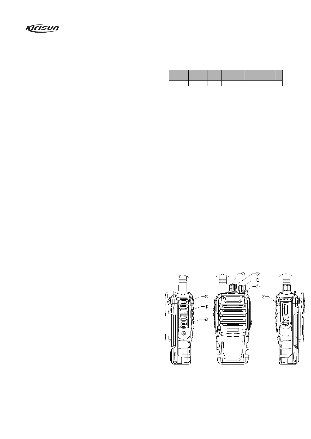
Chapter 2 External View and Functional Keys
2.1 External View
2.2 Functional Keys
① LED Indicator
Lights red while transmitting; lights green while receiving;
flashes red when the radio is in low power.
Page 3
PT6700 Service Manual
3
RF
AMP
5T
TX/RX SW
5T5R
RF
AMP
5C
BUFFERRXVCO
TXVCO
MODE
RIPPLE
FILTER
5C
BUFFER
PLL IC
DATA FROM MCU
CLK FROM MCU
LE FROM MCU
PS FROM MCU
LOCK TO MCU
TCXO
12.8MHz
QT/DQT FROM MCU
CENTER FREQUENCY ADJUST FROM MCU
5C
5C
MIXER
5R
IF
AMP
5R
5C
12.8MHz TO
51.2MHz
DET COLL
51.65MHz
+/- 15KHz
+/- 7.5KHz
450KHz
NOISE
AMP
TA31136NOISE DETBUSY SIGNEL TO MCU
5R
② On/Off/Volume Control Knob
Turn clockwise until you hear a click to turn on the radio. Turn
counterclockwise until you hear a click to turn it off. Rotate it to
adjust the volume after turning on the radio.
③ Channel Selector Knob
Rotate the knob to select channel 1-16.
④ PTT (Push-To-Talk) Button
Press and hold the PTT button and speak into the microphone,
your voice can be sent to the recipient. Release the PTT button to
receive.
⑤ Side Button 1 (programmable button)
⑥ Side Button 2 (programmable button)
⑦ Top Button (programmable button)
⑧ External Speaker/Microphone Jack Cover
Remove the cover; you will see the external
speaker/microphone jack. External speaker/microphone can be
connected to the radio through this jack.
Chapter 3 Circuit Description
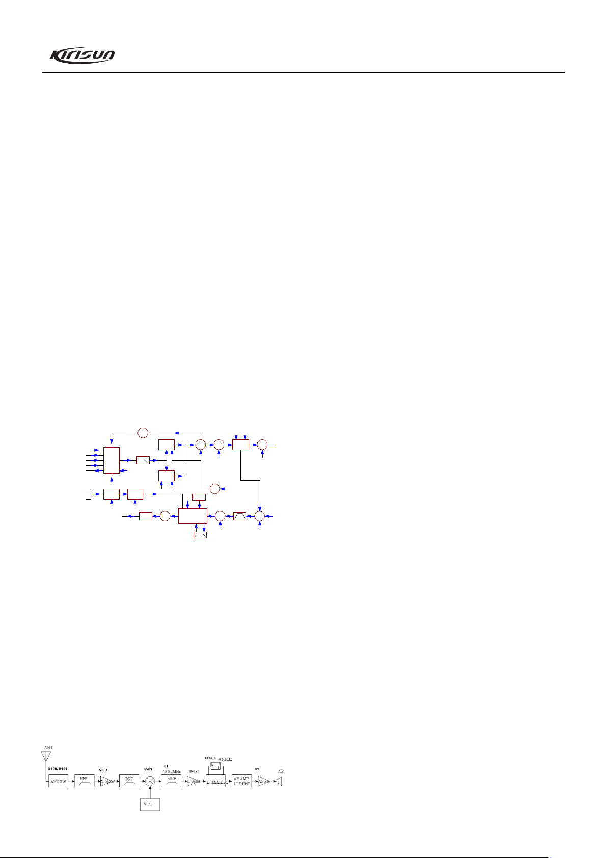
3.1 Frequency Configuration
Figure 3.1 Frequency Configuration
The reference frequency of the frequency synthesizer is
provided by 12.8MHz crystal oscillator X300 TCXO. The receiver
adopts double mixing. The first IF is 51.65MHz and the second IF
is 450kHz. The first local oscillator signal of the receiver is
generated by the frequency synthesizer. The second local
oscillator signal adopts the fourth harmonics (51.2MHz) of the
crystal oscillator X300 (TCXO, 12.8MHz). Transmitter signal is
directly produced by the frequency synthesizer.
3.2 Principle of Receiver (RX)
Figure 3.2 Principle of Receiver
Front end
The signal coming from the antenna passes through the
RX/TX switch circuit (D400, D401, D403 and D404), and passes
through a BPF comprises of C504,C510,L502,L507,C526,
C549,D508,C548,L515,C547,C532,D503,C544 and L513
to remove unwanted out-of-band signal, and is sent to the low
noise amplifier (LNA) consists of Q504 and its peripheral
components to be amplified.
Output signal from the LNA passes through a BPF comprises
of L511,C530,C540,D506,C539,L510,C538,C529,
D505,C537,L509,C536 and D504 and goes to the first mixer
(Q503).
PWM wave is output from pin 12 of the MCU. The wave is
filtered and rectified into adjustable voltage, which can control the
center frequency of the band pass filter through changing capacity
of the varactor diodes (D503, D504, D505, D506, D507, and
D508).
First mixer
The received signal from LNA is mixed with the first local
oscillator signal from the frequency synthesizer to produce the
first IF signal (51.65MHz). Then the first IF signal passes through
crystal filter (Z1) to remove the adjacent channel signal and signal
outside the adjacent channel.
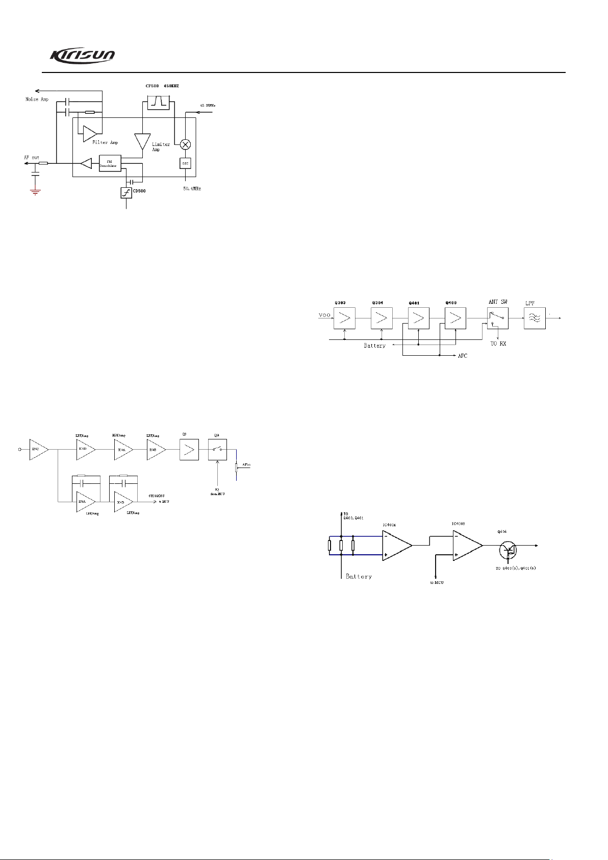
IF circuit
The first IF signal from the crystal filter is amplified by the
first IF amplifier (Q502), and is sent to the IF processing IC
(IC500, TA31136).
IF IC consists of second mixer, second local oscillator, IF
amplifier, limiter, discriminator, and noise amplifier.
The 12.8MHz frequency produced by TCXO (X300) is
multiple-amplified and then the fourth harmonics (51.2MHz) is
adopted as the second local oscillator signal source. The second
local oscillator signal (51. 2MHz) is mixed with the first IF signal
(51.65MHz) in IC500 to generate the second IF (450kHz). And
then the second IF signal is amplified and limited in IC500,
filtered by the ceramic filter (CF500, 450kHz), and demodulated
in IC500 to output audio signal.
Page 4
PT6700 Service Manual
4
Figure 3.3 IF System
Rx audio signal processing
The voice signal processing circuit of the receiver consists of
IC702 and its peripheral circuits. After being amplified in
IC702-C, voice signal from IC500 is sent to IC4 (CTCSS signal
filtering circuit) and IC702-D respectively. The signal is then
amplified, deemphasized and filtered by other units of IC702 to
remove HF and LF components contained in the audio frequency,
with only voice components within 300~3000Hz left. The
resulting signal is then sent to Q701 for amplification. The
amplified signal is adjusted by the volume potentiometer and then
is sent to the audio power amplifier (U2).
Figure 3.4 Audio Processing of Receiver
Squelch circuit
The demodulated signal from IC500 goes to the selective
noise amplifier consists of internal noise amplifier of IC500, C522,
R521, C522 and R516 to remove the noise component. The
resulting signal is then amplified by Q500 and demodulated by
D501 and is sent to the MCU. MCU identifies level of the noise
and controls the squelch.
Audio power amplifier
The audio power amplifier circuit consists of U2 and its
peripheral components.
The received audio signal, voice alert signal, alert tone signal
and warning tone signal are collected and pass through the audio
amplifier where they are amplified and output to drive the speaker.
The volume of the warning tone is not controlled by the preset
volume level of the radio.
When AFCO is in high level, Q707 turns on, U2 starts to
operate, and the speaker makes sound. Speaker impedance: 16Ω.
CTCSS/DCS signal filtering
Audio signal demodulated by IC500 may contain CTCSS
(Continuous Tone Control Squelch System) or DCS (Digital Code
Squelch) signal. The spectrum components of CTCSS/DCS are
within 2-250Hz. The filtering circuit consists of IC4 can remove
signals outside the CTCSS/DCS spectrum, which enables the
MCU to decode CTCSS/DCS more accurately.
3.3 Principle of Transmitter (TX)
TX power amplification
Figure 3.5 Principle of Power Amplifier and Antenna Switch
The modulated RF signal from VCO is amplified by Q303,
Q304 and Q401, and is sent to Q400 for power amplification.
Grid bias of Q400 and Q401 is controlled by the APC circuit.
Through changing the grid bias voltage, the Tx output power can
be controlled conveniently.
APC (Automatic Power Control)
Figure 3.6 APC Circuit
R422, R423 and R424 are used to test the power amplification
current. IC400A is the sampling amplifier for the power
amplification current. IC400B is the power comparator amplifier.
If the Tx output power is too high, the power amplification
current and IC400A output will increase; IC400B output voltage
will decrease, so the bias voltage of Q400 and Q401 will also
decrease, which causes the Tx output power to be lowered, and
vice versa. Thus the Tx output power can keep stable under
different working conditions.
MCU can set the power through changing the voltage input to
IC400B.
Page 5
PT6700 Service Manual
5
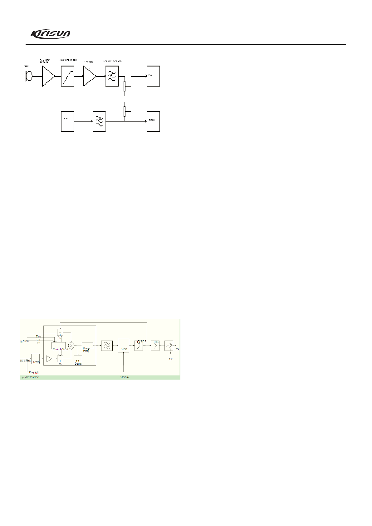
Tx voice signal processing
Figure 3.7 Transmitter Audio Circuit
The Tx voice signal processing circuit consists of IC600 and
its peripheral components. After being amplified, limited and
filtered, the voice signal from MIC is sent to VCO for modulation
together with CTCSS/DCS signal.
The AGC circuit consists of D600, D601 and Q601. When
signal from MIC is too strong, the AGC circuit will lower the
signal strength to make sure that no distortion happens to the
signal.
Q600 is the power switch of the voice processing circuit. It is
controlled by MCU. Power supply of IC7 will be turned on when
the radio is transmitting.
J2 is the jack for external MIC. When using external MIC, the
internal MIC will be turned off automatically. But the internal
PTT is still effective.
3.4 Principle of Frequency Synthesizer
Figure 3.8 Frequency Synthesizer
The radio adopts PLL type frequency synthesizer.
The frequency synthesizer consists of reference oscillator,
voltage control oscillator (VCO), programmable divider, phase
comparator, and low pass filter.
Rx VCO unit consists of Q302, L308, C331, C335, C332、
D301 and D303. Tx VCO unit consists of Q307, L322, C355,
C363, C371, C364, D306 and D308. D304 is the modulation
circuit of VCO.
IC300 (MB15E03) is PLL integrated circuit, which consists of
programmable reference divider, programmable swallowing
divider, phase comparator, and charge pump.
The low pass filter consists of R329, C358, R330, R331, C359,
R332, C356, C365 and C360.
The reference frequency is provided by X300 (TCXO,
12.8MHz).
The reference frequency from TCXO (Temperature
Compensated Crystal Oscillator) is divided by the programmable
reference divider in IC1 to produce reference frequency of 5kHz
or 6.25kHz (determined by the preset channel frequency and is
controlled by MCU).
The oscillation frequency from VCO goes to IC300 where it is
divided by the programmable swallowing divider and is then
compared with the reference frequency to obtain error signal. The
signal is then filtered by a low pass filter and is sent to VCO to
change the oscillation frequency of the VCO, enabling the
frequency to reach the set value. Then the VCO is locked.
N=F
VCO/FR
N: Times of frequency division
F
: Oscillation frequency of VCO
VCO
FR: Reference frequency
Unlock detection: When PLL is unlocked, Pin 14 of IC will
output low level signal to MCU. Then MCU prohibits the
transmitter from transmitting and makes an alert tone.
Q308: Power filter, which provides more purified power for
PLL to reduce noise of the frequency synthesizer.
3.5 Voice Alert Circuit
The radio is provided with voice alert function, which is
especially useful at night or in dark environment.
IC203 is a voice memory chip, which is stored with voices of
channel indication etc. Once the channel selector knob is switched,
the speaker will announce the current channel number. You can
press the preprogrammed “Voice Alert” key to repeat the current
channel number.
If voice alert function is enabled, the speaker will announce
the current channel number once the “Voice Alert” key is pressed
under standby mode. You can switch the voice type by pressing
and holding the “Voice Alert” key while restarting the radio. Do it
repeatedly to switch the voice type in the order of “Chinese
Male-English Male-Chinese Female-English Female-No Alert”.
3.6 Power Supply
The radio uses 7.4V, 1700mAh Li battery. The Tx power
amplification circuit (Q400 and Q401) and the Rx audio power
amplifier (U2) directly adopt the battery for power supply. Power
Page 6

PT6700 Service Manual
6
No.
Frequency
[Hz]
No.
Frequency
[Hz]
No.
Frequency
[Hz]
No.
Frequency
[Hz]
1
67.0
11
94.8
21
131.8
31
186.2 2 69.3
12
97.4
22
136.5
32
192.8
3
71.9
13
100.0
23
141.3
33
203.5 4 74.4
14
103.5
24
146.2
34
210.7
5
77.0
15
107.2
25
151.4
35
218.1 6 79.7
16
110.9
26
156.7
36
225.7 7 82.5
17
114.8
27
162.2
37
233.6
8
85.4
18
118.8
28
167.9
38
241.8
9
88.5
19
123.0
29
173.8
39
250.3
10
91.5
20
127.3
30
179.9
EEPROM
D/A
chananl
SW
PTT
MONI
ALARM
PF1
CTCSS/DCS IN
SQL
BATT
VCCN
CTCSS/DCS
BEEP
LE
DATA
CK
to PLL
VIOCE CHIP
TX/RX CONTROL
RXD
TXD
to PC
UL
5TC
5RC
SAVE
APC CONTR
SHIFT
IC200
IC203
MCU
of other circuits is supplied by 5V regulated voltage.
IC100: 5V low dropout, micro-power regulator, which
supplies 5V power with large current for the radio together with
Q104.
Q100: 5T switch, which is controlled by MCU.
5T: Supplies power for front end of Tx.
Q102: 5R switch, which is controlled by MCU.
5R: Supplies power for RF amplifier, mixer, IF processing unit,
and audio signal processing unit etc. of the receiver.
Q103: 5C switch, which is controlled by MCU.
5C: 5V power supply under SAVE control. Supplies power for
frequency synthesizer.
3.7 MCU Unit
Figure 3.9 Principle of MCU Unit
MCU unit controls the operation of each unit of the radio so
that all functions can be realized.
Communicate with external PC.
Access the status data of the radio.
Control the PLL to generate Rx and Tx local oscillator
frequencies.
Obtain status parameters of current channel.
Control status of LED indicator.
Control power supply for each unit.
Check the actions of each functional key.
Generate CTCSS signal.
Generate DCS signal.
Generate power control signal.
Perform CTCSS decoding.
Perform DCS decoding.
Test and control the squelch.
Control content of voice alert.
Memory (E2PROM, AT24C08):
The memory is stored with channel data, CTCSS/DCS data,
other function setting data, and parameter adjusting data.
CTCSS/DCS signal encoding and decoding:
The CTCSS/DCS signal (output from pin 12) generated by
MCU is filtered by R155, R156, C242 and C243. Then the
resulting signal is divided into two parts and sent to VCO and
TCXO respectively for modulation.
The CTCSS/DCS signal from the receiver is sent to MCU (pin
49) for decoding. MCU checks if the CTCSS/DCS signal in the
received signal matches the preset value of the radio, and
determines whether to open the speaker or not.
Power adjustment:
Output from pin 42 of the MCU passes through integrating
filter (R161, C317, R206, and C318), and is sent to the APC unit
to control the output power of the transmitter.
CTCSS
CTCSS (Continuous Tone Control Squelch System) is a
squelch control system which is modulated on carrier and is
guided by a continuous sub-audio signal. If CTCSS is set, the
communication between the transmitting and receiving radios can
be realized only when the two radios have set the same CTCSS
frequency. In doing this, disturbance from other signals can be
avoided.
PT6700 has 39 groups of standard CTCSS frequencies for
your selection. See table 3.1.
The CTCSS signal is generated by MCU, and is passed
through low pass filter consists of RC to remove high frequency
components (above 300Hz). Then the resulting signal is sent to
VCO for modulation.
Table 3.1 CTCSS Frequencies
Page 7
PT6700 Service Manual
7
023
114
174
315
445
631
025
115
205
331
464
632
026
116
223
343
465
654
031
125
226
346
466
662
032
131
243
351
503
664
043
132
244
364
506
703
047
134
245
365
516
712
051
143
251
371
532
723
054
152
261
411
546
731
065
155
263
412
565
732
071
156
265
413
606
734
072
162
271
423
612
743
073
165
306
431
624
754
074
172
311
432
627
No.
Port
name
Pin
Name
I/O
Function
1
NC
NC 2 AFCO2
P35 O Audio frequency switch 2
3
GLED
P33 O Green LED switch
4
PTT
P34 I [PTT] input
5
MODE I
Connect the 4.7K resistor with VCC, programming test
point 6 VDEVC2
P43 O VHF deviation switch 2
7
VDEVC1
P44 O VHF deviation switch 1
8
RST I
Reset input, programming test point
9
XOUT O
10
VSS I
GND, programming test point
11
XIN I
Oscillator (7.3MHz)
12
VCC I
5V CPU power input, programming test point
13
SHIFT
P27 O Clock beat shift. H: On
14
VCCN
P26
O(PWM)
Frequency stability output
15
TO
P25
O(PWM)
QT/DQT output
16
WNTC
P24
O
Wideband/Narrowband control
H: Wideband, L: Narrowband
17
APC
P23
O(PWM)
TX: Automatic power control output, RX: 0
18
TUNE
P22
O(PWM)
TX: 0 RX: BPF tuning output
19
BEEP
P21
O(PWM)
BEEP/DTMF output
20
SDA
P20
I/O
EEPROM data line
21
ENC0
P17 I Encoder input
22
ENC2
P16 I Encoder input
23
ENC3
P15 I Encoder input
24
ENC1
P14 I Encoder input
25
SCL
P13 O EEPROM clock line
26
NC
NC
27
UL
P45
I
PLL circuit unlock detect pin
H: locked, L: unlocked
28
TXD
P66 O RS-232C output, programming test point
29
RXD
P67 I RS-232C input, programming test point
30
CK
P12 O PLL clock output
31
DT
P11 O PLL data output
32
LE
P10 O PLL IC enable pin, H: locked
33
RX
P31 O Receiving enable
34
BUSY_V
P30 O Busy signal of voice annunciation IC
35
DATA_V
P65 O Data of voice annunciation IC
36
SCLK_V
P64 O Clock of voice annunciation IC
37
RLED
P63 O Red LED control, H: On
38
NC
P07
I(A/D0)
Connect the pull-up resistor with VCC, and connect the
pull-down resistor with VSS
39
NC
NC
40
NC
NC
41
TI
P06
I(A/D1)
QT/DQT signal input
42
BUSY
P05
I(A/D2)
Busy signal input
43
BATT
P04
I(A/D3)
Battery voltage detect
44
VREF I
Connect with VCC
45
SAVE
P60
O
Battery saving control, H: supply power, L: power
saving
46
MUTE
P62 O Mute control H: Mic mute L: audio mute
47
5RC
P61 O Receiving power control L: On
48
KEYIN
P03
I(A/D4)
Programmable key P1, P2, P3 detect
49
5TC
P02 O Transmitting power control, H: On
50
RLED
P01 O Red LED switch
51
AC
P00
O
Alarm switch control, H: controlled by volume switch
Radio should be in low level in emergency alarm
52
AFCO1
P37 I Audio control switch 1
Position
Mark
Model
Function Description
1
IC300
MB15E03
Frequency synthesizer
2
IC701
NJM2904
APC, voltage comparison, driving
DCS
DCS (Digital Code Squelch), which is used to control squelch,
is a series of continuous digital codes modulated on carrier
together with voice signal. If DCS is set, the speaker can be
opened only when the radio receives signal with the same DCS to
avoid disturbance of unwanted signals.
PT6700 has 83 standard codes (inverted and non-inverted) for
your selection. See table 3.2.
DCS signal is produced by MCU (in waveform of PWM). It
passes through the low pass filter consists of RC to remove the
high frequency components (above 300Hz). Then the resulting
signal is sent to VCO and TCXO for modulation, with HF
components of the DCS signal being modulated by VCO, and the
LF components of the DCS signal being modulated by TCXO.
The CTCSS/DCS signal coming from the receiver is sent to
MCU for decoding. MCU checks if the DCS code in the received
signal matches the preset DCS of the radio, and determines
whether to open the speaker or not.
Table 3.2 DCS Codes
3.8 Semiconductor Data
Refer to table 3.3 for descriptions of each pin.
Table 3.3 Definition of CPU Pins
Table 3.4 Function Description of Semiconductor Components
Page 8
PT6700 Service Manual
8
3
IC500
TA31136
Rx second local oscillation, second IF
amplification, limitation, demodulation, and
noise amplification
4
IC702
NJM2902
Amplification and filtering of demodulation
signal of receiver.
5
IC600
NJM2902
MIC amplification, limitation and filtering
6
U2
TDA2822
Audio frequency power amplification of
receiver
7
IC200
AT24C08
E2PROM, memorizes channel frequency data,
function setting parameters and adjusting status
parameters
8
IC201
R5F212A8
MCU
9
IC202
PST9140NR
MCU reset circuit
10
IC100
HT7150-1
LDO, low-power voltage regulator
11
IC203
W588A080
Voice storage IC
12
Q402
2SC5108
First amplification of transmitter
13
Q403
2SC3356
Second amplification of transmitter
14
Q304
2SC5108
VCO buffer amplifier
15
Q303
2SC5108
VCO buffer amplifier
16
Q308
2SC4617
VCO power supply filter
17
Q500
2SC4738
Noise amplifier
18
Q701
2SC4617
Audio frequency signal amplification of receiver
19
Q400
2SK3476
Transmitter final power amplification
20
Q401
RD01MUS1
Transmitter power amplification driving
21
Q404
DTA144EE
APC output switch
22
Q503
3SK318
First mixer
23
Q504
3SK318
Receiver high power amplifier
24
Q502
KTC4082
1st IF Amplifier
25
Q200
DTC144EE
Red LED Driving
26
Q201
DTC144EE
Green LED Driving
27
Q601
2SK1824
Voice alert switch
28
Q100
KTA1298
5T switch
29
IC102
KTA1298
5R switch
Position Mark
Model
Function Description
D400
MA77
Transmitter antenna switch diode
D401
HVC131
Transmitter antenna switch diode
D402
HSC277
VCO output switch
D403
HVC131
Antenna toggle switch
D301
HVC376B
VCO oscillation varactor diode
D303
HVC376B
VCO oscillation varactor diode
D304
MA360
VCO modulation diode
D405
HZU5ALL
APC output voltage-limiting diode
D309
MA2S111
Unlock detection diode
D310
MA2S111
VCO oscillation varactor diode
D501
1N4148
Noise demodulation
D202
GREEN LED
Receiving indicator
D509
MA2S111
APC single diode
D201
RED LED
Transmitting indicator
D202、D203
GREEN LED
Receiving indicator
Item
Rated Value
Nominal center frequency
51.65MHz
Pass band width
±7.5kHz or higher but within 3dB
40dB stop band width
±20.0kHz or lower
Pulse within band
1.0dB or lower
Insertion loss
3.0dB or lower
Guarantee attenuation
80dB or higher, within f0-910kHz
Terminal impedance
1.2kΩ
Item
Rated Value
Nominal center frequency
450kHz
6dB band width
±6kHz or higher
50dB band width
±12.5kHz or lower
Pulse
2.0dB or lower, within f0±4kHz
Insertion loss
6.0dB or lower
Guarantee attenuation
35.0db or higher, within f0±100kHz
Terminal impedance
2.0kΩ
Mode
Function
How to enter
User Mode
For normal use
Power ON
PC
Mode
Data
Programming
Mode
Used to read and write
frequency data and
other features to and
from the radio
Received commands
from PC.
PC Test Mode
Tune the radio
parameters by PC
Received commands
from PC.
Firmware
Programming
Mode
Upgrade the radio
when new features are
released
Press and hold the top
key for over 2 seconds
while turning the radio
power ON, and received
commands from PC
Wired Clone Mode
Used to transfer
programming data
from one radio to
another
Press and hold side key 1
for over 2 seconds while
turning the radio power
ON
3SK31 8
M: YB-
G1
G2
D
S
G
S
D
CC
C
C
B
B
B
B
E
E
E
E
G
D
S
2SK18 24
Mark: B1
2SC510 8
M: MC
C
B
E
M: R24
2SC335 6
C
B
E
2SC461 7
C
B
E
C
B
E
2SC473 8
KTC4082
C
B
E
2SC162 3
M: L6
KTA12 98
DTC144EE
M:16
GNDINOUT
HT7150 -1
RD01MUS1
D
G
S
S
RD07MVS1
RDA000 2
1
2
3
DA2 21
M: K
2SK30 8N V
DTA14 4EE
C
B
E
FMMT591
GSD
Table 3.7 Features of CF500LTVPC450EB
Table 3.8 Schematic Diagram for Packaging of Semiconductor
Devices
Table 3.5 Function Description of Diodes
Mode Introduction
Chapter 4 Mode Introduction
Table 3.6 Features of Crystal Filter Z1
4.1 User Mode
You can enter User Mode (conventional communication mode)
by turning the radio power ON. Under this mode, users can use
the defined functions of the radio.
4.2 Data Programming Mode
Page 9
PT6700 Service Manual
9
Computer
(RS232 serial port)
Programming
cable
Radio
(Earphone/Program
ming interface)
The radio has been set before leaving the factory. However,
due to different requirements of users, the radio’s operating
frequencies, channels, CTCSS/DCS, scan, and other functional
parameters should be reprogrammed. Therefore, Kirisun has
specially designed a set of Chinese/English programming software
KSP6700 with friendly interface, convenient operation and
visualized display for setting functional parameters of the radio.
Steps for setting the functional parameters of the radio by PC
are as follows:
A. Install KSP6700 on the computer.
B. Connect the radio to the serial port of the PC with the
special programming cable (KSPL-U08). Refer to the
figure below.
Figure 4.1
C. Turn on the computer.
D. Turn on the radio.
E. Run the KSP6700 programming software by double
clicking on its executive program.
F. Click “Program” in the main menu of KSP6700, and
click “Read” in the pull-down menu to read parameters
of the radio to the computer; click “Write” in the
pull-down menu to write parameters in the computer to
the radio.
G. The following parameters can be set by using KSP6700
according to requirements of the user:
Radio Information:
Radio Model (model/frequency range), Serial Number,
Embedded Information, MCU Version, Hardware Version, etc.
Radio Parameters:
1) Key Assignment: Side Button 1, Side Button 2, Top Button
can be set as long/short key and the hold time can be defined.
2) Optional Functions
1. Wired Clone enable
2. TOT All Low Power Switch
3. TOT Reset Time Firmware Programming Mode enable
4. TOT Pre-alert Beep Tone
5. TOT Rekey Time All Low Power
6. Squelch Level Selection
7. Voice Annunciation Setting Battery Save
8. Password of Read Radio
9. Password of Write Radio
3) Scans
Scan function setting: Priority Channel selection, Revert
Channel selection, Tx Dwell Time, Dropout Delay Time,
Lookback Time.
4) Emergency Setting
Channel Parameter:
(1) CH Rx frequency and Tx frequency (Step value:
2.5kHz/5kHz/6.25kHz)
(2) CH Rx signaling and Tx signaling.
a) None
b) CTCSS (60~260Hz @ 0.1Hz step)
c) DCS(-777 ~ 777 @ octal umber)
(3) Busy channel lockout selection
(4) Clock beat control
(5) Channel spacing 25kHz/12.5kHz (Wide/Narrow) selection
(6) Add/delete scan list
(7) High/low power level selection
(8) QT Reverse
For detailed operation, please refer to “Help” of KPS6700
programming software.
Note:
1. Firstly, please read data of the radio and back up the data before
editing the parameters on KSP6700.
2. If the radio cannot function normally after being written in with
the edited data, please rewrite the backup data into the radio.
3. “Model Information” is important for the radio; users should
not modify it.
4.3 PC Test Mode
Connect the radio to the serial port of the computer with the
special programming cable. Please refer to Figure 4.1.
Warning: Non-professionals should not enter PC Test Mode;
otherwise, the radio may be damaged. Before entering the PC Test
Mode, please firstly connect a 50Ω high frequency load to the
antenna connector of the radio or connect the radio to a general
test set.
In the programming software, enter the Tuning Mode under
the PC Test Mode to tune the following parameters of the radio:
1) Frequency Stability
2) Five frequency points of Tx High Power
3) Five frequency points of Tx Low Power
4) Five frequency points for SQL9 On (Wideband)
5) Five frequency points for SQL9 Off (Wideband)
6) Five frequency points for SQL9 On (Narrowband)
Page 10
PT6700 Service Manual
10
7) Five frequency points for SQL9 Off (Narrowband)
8) Five frequency points for SQL1 On (Wideband)
9) Five frequency points for SQL1 Off (Wideband)
10) Five frequency points for SQL1 On (Narrowband)
11) Five frequency points for SQL1 Off (Narrowband)
12) Five frequency points for QT (67.0Hz) Deviation
(Wideband)
13) Center frequency point for QT (67.0Hz) Deviation
(Narrowband)
14) Five frequency points for QT (151.4Hz) Deviation
(Wideband)
15) Center frequency point for QT (151.4Hz) Deviation
(Narrowband)
16) Five frequency points for QT (254.1Hz) Deviation
(Wideband)
17) Center frequency point for QT (254.1Hz) Deviation
(Narrowband)
18) Five frequency points for DQT Deviation (Wideband)
19) Center frequency point for DQT Deviation (Narrowband)
20) Five frequency points for Rx Sensitivity
21) Tx Low Voltage
4.4 Firmware Programming Mode
The radio is in possession with an internal Flash ROM which
can be upgraded when new features are released.
Procedure:
1. Press and hold the Top Key for over 2 seconds while turning the
radio power ON. The LED will light orange and the radio enters
the Firmware Programming Mode.
2. Run the firmware programming software KMU on PC.
3. Connect the radio to the computer by the programming cable.
4. Select a COM port and load the firmware upgrading file. Then
click on “E.P” to start downloading.
5. If the communication ends successfully, turn the radio power
OFF to exit.
6. If you want to continue programming other radios, repeat steps
1 to 5.
4.5 Wired Clone Mode
If the wired clone function is enabled, the radio can enter the
Wired Clone Mode. After entering this mode, the radio will not
exit automatically. The user needs to restart the radio if he wants
the radio to return to the User Mode.
The operation procedure is as follows:
1. Press and hold Side Button 1 while turning the radio power ON
to enter the Wired Clone Mode. If the wired clone function is
disabled, the radio will enter User Mode.
2. Connect the slave radio to the master radio by the cloning cable
and turn on the power of the slave radio.
3. Press Side Button 2 of the master radio to start cloning. The
LED on the master radio will light red, and the data of the master
is sent to the slave. While the slave is receiving the data, the LED
lights green. When cloning of data is completed, the LED of the
master will go out, and the slave will restart automatically.
4. Carry out the operation in step 3 to clone other slave radios.
Note: The user can enable or disable the wired clone function
through PC programming software. Once the wired clone function
is disabled, the radio cannot enter the Wired Clone Mode.
Chapter 5 Disassembly for Repair
The radio is a piece of precision communication equipment.
Please be careful when disassemble the radio during service. The
instructions for the disassembly are as follows.
5.1 Attaching and Removing the Battery
1) Attaching the Battery
Fit the two extensions at the top of the battery into the slots at
the top of the radio’s body.
Press the bottom part of the battery towards the radio until a
click is heard and the battery is hooked.
2) Removing the Battery
Push the battery latch at the bottom of the radio forward, the
bottom part of the battery will bounce up automatically. Then
release the belt clip and remove the battery from the radio’s body.
Note:
* Do not short-circuit the battery terminals or dispose battery
in fire.
* Do not disassemble the battery casing by yourself.
5.2 Installing the antenna
Page 11
PT6700 Service Manual
11
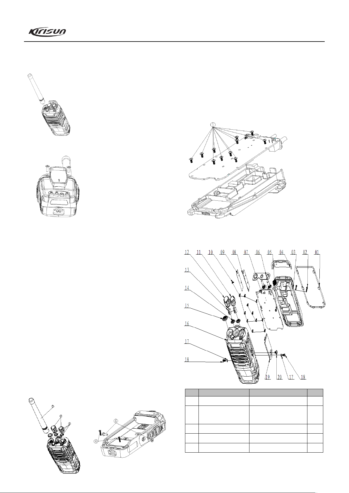
No.
Name
Part number
Pcs
1
7MHR-7069-04A-W0
Main Waterproof Loop
1
2
7SMF-020080M-MH
HT-N1
M2*8 Machine Screws
1
3
Al cabinet assembly
1
4
7MHP-7069-02A-W0
Top Cover
1
5
7MHR-1727-09A-W3
MIC Seal
1
Hold the base of the antenna, and rotate it clockwise to the
connector on the top of the radio until it secures.
5.3 Installing the belt clip
5.4 Removing the mainboard from the Al chassis
1. Remove 11 screws on the PCB by a cross screwdriver;
2. Remove the solder of the antenna connector with a soldering
iron, and remove the mainboard.
See figure below:
Match the two holes of the belt clip with those on the rear of
the radio, and then fix the belt clip to the radio using the two
supplied screws. Loose the fixing screws to remove the belt clip.
5.4 Removing the chassis from the front cabinet
1. Remove the antenna;
2. Pull out the volume knob and the channel selector knob.
3. Remove the two nuts for knobs and the nut for the antenna
connector by the special tool;
4. Remove the two fixing screws at the lower part of the Al
chassis and remove the two fixing screws on two sides of the
cover;
5. Insert a flat-blade screwdriver into the slot at the bottom of
the Al chassis, and prize it up. Then pull the Al chassis
backwards to remove it from the front cabinet. Be careful not
to break the speaker wire.
See figure below:
5.5 Exploded View
Page 12

PT6700 Service Manual
12
6
7MHR-7210-02A-W0
PT6700 Top Waterproof
Gasket
1
7
Mainboard assembly
1
8
PTT PCB
1
9
7MHS-7069-04A-W
PT7800 PTT key
1
10
7SMF-020040M-SZY
B-N
M2*4 Screws
12
11
7MHP-7210-04A-W0
Volume Knob
1
12
7MHP-7210-03A-W0
Channel Selector Knob
1
13
7MHS-1140-01A-W
Circlip for knob
2
14
7NRC-060100035-B
1
Nut for knob
2
15
7NRC-090115025-G1
Nut
1
16
Front cover assembly
2
17
7MHR-7069-08A-W0
O-type gasket
2
18
7SMF-025080M-SZY
B-Z1
M2.5*8 Screws
2
19
7MHP-7210-02A-W0
MIC cover
1
20
1
No.
Name
Part No.
Pcs
1
7MHP-7210-01A-W0
Front cover
1
2
7MHP-7069-03A-W0
PTT Side cover
1
3
7MHP-7069-04A-W0
PTT cover
1
4
7MHP-7069-06A-W0
Battery latch
1
5
7MHP-7069-10A-WC
Light guide
1
6
7MHR-7069-02A-W0
PTT key
1
7
7MHR-7210-01A-W3
Emergency key
1
8
7GCJ-S1867-01
Paste for earphone PCB
board
1
9
7MHS-1010-02A-N
Spring
2
10
7GCB-3950001
φ 39.5 Speaker net
1
11
4SS7-4564-016-100
φ 45 Speaker
1
12
7MHS-7210-01A-W
Fixed sheet for speaker
1
13
7GCB-070045005-J
3 对讲机 Φ7 话筒布
1
14
7SMF-020040M-SZY
B-N
M2*4 Machine screw
1
15
6PD7-1867-HLC
Earphone PCB board
1
16
6PF7-1867-HLC
7200 耳机连接软板
1
No.
Name
Part number
Pcs
1
7MHL-7069-01A-W
Al bracket
2
3CR7-SMA-50JFB-4
RF co-axis connector
3
7SMF-020040M-SZYB
-N
M2*4 machine screw
4
7MHR-7069-07A-W0
water-proof gasket for
bracket
5
7MHR-7069-05A-W3
Water-proof gasket for
dormer
6
7MHF-7069-02A-W
dormer cover
No.
Name
Specifications
1
Computer
P2 or above, IBM compatible PC, WINDOWS
98/ME/2000/XP Operating System
2
Programming
software
KSP6700
3
Programming
cable
4
Clone cable
KCL01
5
DC regulated
power supply
Output voltage: 13.8V
Output current: ≥ 20A
6
RF power
meter
Measurement range: 0.5-10W
Frequency range: 100MHz-500MHz
Impedance: 50Ω
SWR ≤ 1.2
7
Frequency
counter
Frequency range: 0.1-600MHz
Frequency accuracy: better than ±1×10⁻⁶
Sensitivity: better than 100mV
8
Deviation
Frequency range: DC600MHz
Front cover assembly:
Chapter 6 Adjustment
Before test/adjustment, make sure all equipment has been
grounded!
Before test/adjustment, make sure the antenna output
terminal has been correctly connected to corresponding equipment
or load!
The transmitter output terminal must be terminated with an
RF power attenuator and connected to a standard signal generator
(SSG)/frequency counter/deviation meter/spectrum analyzer!
Make sure no transmission operation is being conducted
while measuring the receiver!
During the adjustment/test/maintenance, make sure reliable
anti-static measures are taken for human body and equipment.
6.1 Equipment and Software Required for Test and
Adjustment
Equipment and software listed in Table 6.1 are required for test
and adjustment of PT6700.
Table 6.1 Equipment and Software Required for Test and
Adjustment
Al cover assembly:
Page 13

PT6700 Service Manual
13
meter
Measurement range: 0 - ±5kHz
9
DMM
Input impedance: above 10MΩ/V DC, capable of
measuring voltage, current and resistance.
10
Audio signal
generator
Frequency range:2-3000Hz
Output level: 1-500mV
11
RF power
attenuator
Attenuation: 40dB or 50dB
Supporting power : higher than 50W
12
Standard signal
generator
Frequency range:10MHz-1000MHz
Output level: 0.1uV-32mV (-127dBm~-17dBm)
13
Oscilloscope
Frequency range: DC~20MHz
Test range: 10mV-20V
14
Audio
frequency
voltmeter
Test range: 10mV-10V
Low Freq Point
Intermediate Freq
Point
High Freq Point
PT6700
420.125MHz
445.125MHz
469.975MHz
Recommendation: Item 6, 7, 8, 10, 11, and 12 listed in the table
can be replaced by HP8920 general test set.
Figure 6.1 External Speaker/Microphone Interface Definition
6.2 Adjustment
After changing components during the maintenance, it is
necessary to test the radio and adjust its technical parameters. The
following part is going to introduce the adjustment items.
Some parameters can be adjusted by use of KSP6700
programming software (in the Tuning Mode). The adjustable
parameters are as follows:
1) 6250Hz Precision
2) 2500Hz Precision
3) Tx Power
4) Tx Low Voltage
5) Squelch Level
6) QT Deviation
7) DCS Deviation
8) Rx Sensitivity
Steps for adjustment:
a. Enter PC Test Mode. Refer to Section 4.2.1.
b. Click “Edit” in the main menu of KSP6700 programming
software, and then click “Entry Tuning” in the pull-down menu to
enter the Tuning Mode.
c. Then the “Tuning Item List” screen will pop up. Double
click the item you want to adjust, and then you can adjust the
parameters.
d. Exit the PC Test Mode after adjustment.
6.3 Adjustment
6.3.1 VCO
Disable the “Battery Save” function, and set the Rx frequency
at the high frequency point (see Table 6.2). Under the receiving
status, measure the voltage of PD by DMM. Then adjust the PD
voltage to be 4.0V±0.2V by tuning the trimming capacitor C371.
Set the Tx frequency at the low frequency point (see Table
6.2), and press the PTT button. Then measure the voltage of PD
by DMM. The resulting voltage should be higher than 0.5V.
Table 6.2 High/Intermediate/Low Frequency Point for PT6700
6.3.2 PLL frequency
1. In the Tuning Mode, double click “6250Hz precision” to
enter. Adjust the parameter among 0-255 to make the Tx
frequency at the rated value (error within ±200Hz).
2. In the Tuning Mode, double click “2500Hz precision” to
enter. Adjust the parameter among 0-255 to make the Tx
frequency at the rated value (error within ±200Hz).
6.3.3 Tx Power
In the Tuning Mode, double click Tx “High power” to enter.
Adjust the five frequency points of “Lowest”, “Low”, “Mid”,
“High” and “Highest” among 0-255 to make the Tx power at 4W.
Meanwhile, observe the operating current, and make sure that the
current ≤1.8A.
In the Tuning Mode, double click Tx “Low power” to enter.
Adjust the five frequency points of “Lowest”, “Low”, “Mid”,
“High” and “Highest” among 0-255 to make the Tx power higher
than 0.5W.
6.3.4 Tx Low Voltage
Firstly, adjust the power voltage to be 6.8V. Double click “Tx
low voltage” in the Tuning Mode to enter. The software will test
automatically. When the value changes no more or only changes a
little, click SAVE to exit.
6.3.5 Deviation
Input audio signal (120mV, 1000Hz) to the MIC jack of the
radio. Adjust the potentiometer VR2 to make the Tx deviation at ±
4.2kHz.
6.3.6 DCS Tx Signal Waveform and Deviation
In the Tuning Mode, double click “DCS DEV” to enter. Adjust
Page 14

PT6700 Service Manual
14
Item
Test Condition
Test Equipment
Measurement Point
Parts to be adjusted
Requirements
Remark
Setting
BATT terminal voltage: 7.5V
DMM
CV
VCO lock voltage
CH: Rx high freq point
C180
4.0V±0.2V
Adjust
CH: Tx high freq point
4.0V±0.2V
Adjust
Item
Test
Condition
Test Equipment
Measurement
Terminal
Adjustment
Parts
Requirement
Remark
Audio level
Test freq: Mid freq
point
Antenna input:
RF OUT: -53dBm
(501μV)
MOD: 1kHz
DEV: ±3.0kHz
RF signal
generator
Oscilloscope
Audio frequency
voltmeter
Speaker
connector
(Turn the volume knob
clockwise to the end)
Audio power > 1.2W
the potentiometer VR1 and observe the demodulation signal (the
waveform should be smooth and similar to square wave). Click
wideband, and adjust the five frequency points of “Lowest”,
“Low”, “Mid”, “High”, and “Highest” to make the deviation at
0.75kHz. Then click narrowband, and adjust the value to make the
deviation at 0.35kHz.
6.3.7 CTCSS Deviation
In the Tuning Mode, double click “QT (67.0) DEV” to enter.
Click wideband, and adjust the five frequency points of “Lowest”,
“Low”, “Mid”, “High”, and “Highest” to make the deviation at
0.75kHz. Then click narrowband, and adjust the value to make the
deviation at 0.35kHz.
In the Tuning Mode, double click “QT(2541) DEV” to enter.
The tuning method is the same as that of “QT(670) DEV”.
6.3.8 Receiver Sensitivity
In the Tuning Mode, double click “Sensitivity” to enter. Adjust
the five frequency points of “Lowest”, “Low”, “Mid”, “High”,
and “Highest” among 0-255 to make the sensitivity be the highest.
6.3.9 Receiver Squelch
In the Tuning Mode, double click “SQL9 On” to enter. Click
wideband and use the following method to adjust the five
frequency points of “Lowest”, “Low”, “Mid”, “High”, and
“Highest” respectively. Firstly, click one of the frequency points,
and adjust the RF signal frequency of the test equipment to be the
same with the receiving frequency of that frequency point, and
adjust the signal level to be -116dBm. Then adjust the frequency
of the modulation signal to be 1kHz and the deviation to be 3kHz.
6.4 Adjustment Description
See Table 6.3, 6.4, and 6.5.
Table 6.3 VCO
The programming software will adjust the value automatically.
When the value keeps stable, the adjustment of that frequency
point is completed. Then click the next frequency point to do the
adjustment. After all of the five frequency points are adjusted, use
the same method to adjust the five frequency points for
narrowband. The only difference is that the frequency of the
modulation signal should be 1kHz, and the deviation should be
1.5kHz.
In the Tuning Mode, double click “SQL9 Off” to enter. Click
wideband and use the following method to adjust the five
frequency points of “Lowest”, “Low”, “Mid”, “High”, and
“Highest” respectively. Firstly, click one of the frequency points,
and adjust the RF signal frequency of the test equipment to be the
same with the receiving frequency of that frequency point, and
adjust the signal level to be -118dBm. Then adjust the frequency
of the modulation signal to be 1kHz and the deviation to be 3kHz.
The programming software will adjust the value automatically.
When the value keeps stable, the adjustment of that frequency
point is completed. Then click the next frequency point to do the
adjustment. After all of the five frequency points are adjusted, use
the same method to adjust the five frequency points for
narrowband. The only difference is that the frequency of the
modulation signal should be 1kHz, and the deviation should be
1.5kHz.
In the Tuning Mode, double click “SQL1 On” and “SQL1
Off” to enter respectively. Use the same method stated above to do
the adjustment. The only difference is that the RF signal level for
“SQL1 On” should be 123dBm, and the RF signal level for
“SQL1 Off” should be 125dBm.
Table 6.4 Rx Part
Page 15

PT6700 Service Manual
1
Audio load: 16Ω
Distortion
meter/General test
set
Sensitivity
CH: Mid freq point
CH: Low freq point
CH: High freq point
RF OUT: -119dBm
(0.25μV)
MOD: 1kHz
DEV: ±3.0kHz
PC Tuning
Mode
SINAD: 12dB or higher
SQL On
sensitivity
CH: Rx center freq
point
PC Tuning
Mode
Normal squelch on after
adjustment
Level 9
RF OUT: -116dBm
Level 1
RF OUT: -123dBm
Item
Test condition
Test equipment
Measuring
terminal
Adjustment
parts
Requirement
Remark
Tx frequency
Frequency counter /
General test set
Antenna
PC Tuning
Mode
Within ±200Hz
DCS waveform
(balance)
Oscilloscope /
General test set
VR1
Smooth and similar to
square wave
Power
Power: 7.5V
Power meter/ General
test set
Ammeter
PC Tuning
Mode
Adjust to 4W
Within
±0.2W
Max. modulation
deviation
CH:Tx center
freq point
AG:1kHz/220mV
Deviation meter/
General test set
VR2
Adjust to ±4.2kHz
±200Hz
Modulation
sensitivity
CH:Tx center
freq point
AG:1kHz/22mV
Deviation checked
should be
2.2kHz~3.6kHz
CTCSS DEV
CTCSS:67Hz
Deviation meter/
General test set
PC Tuning
Mode
Adjust to ±0.75kHz
±50Hz
DCS DEV
DCS:023N
Deviation meter/
General test set
PC Tuning
Mode
Adjust to ±0.75kHz
±50Hz
Low battery
warning
Battery terminal:
6.8V
PC Tuning
Mode
Indicator flashes after
adjustment
Product Model
PT6700
Frequency
136 ~ 174 MHz
400 ~ 450MHz
420 ~ 470 MHz
Number of Channels
16
Channel Spacing
W: 25 kHz /N:12.5kHz
Operating Temperature
-25℃~ +55℃
Antenna Impedance
50Ω
Frequency Stability
±2.5ppm
Sensitivity (12dB SINAD)
0.25μV(W) / 0.28μV(N)
Adjacent Channel Selectivity
W: ≥ 70dB / N:≥ 60dB
Intermodulation Interference
≥ 65dB
Audio Output Power
1W (16Ω)
Audio Distortion
≤ 5%
Tx Power
4W(UHF) / 5W(VHF)
Modulation Type
W:16KφF3E / N:11KφF3E
Clutter and Harmonic
≤-36 dBm
Residual FM(300~3000Hz)
W:≤-45 dB / N:≤-40dB
Audio Distortion(300~3000Hz)
≤ 5%
Adjacent Channel Power
W:≥ 70dB / N:≥ 60dB
Max. Deviation
W: <±5kHz / N: <±2.5kHz
Table 6.5 Tx Part
Chapter 7 Specifications
7.1 General Specifications
7.2 Receiver Section
7.3 Transmitter Section
Page 16

PT6700 Service Manual
17
No.
Problem
Causes and Solutions
1
No display after
switching on
the radio
A. Battery power may be insufficient, please recharge
or change the battery pack.
B. The power switch is broken, please change it.
C. The CPU is broken, please change the IC.
D. The regulator tube IC100 is broken, please change
the IC.
2
PLL
unlocked
(Beeping)
A. The PLL crystal oscillator X300 is broken. Please
change it.
B. The oscillator transistor Q302 and Q307 are
broken. Please change them.
C. The PLL IC300 is broken. Please change it.
3
Cannot talk to
or hear other
group members
A. The frequencies of both users are not the same,
select the same frequency channel.
B. The CTCSS/DCS of both users are not the same.
Please reset it with PC.
C. The radio is out of the effective communication
range.
4
Cannot receive
signals
A. The antenna is in poor contact. Please fasten the
antenna until secure.
B. The sensitivity is too low, please adjust it with PC.
C. The HF amplifier Q504 is broken. Please change
it.
D. The squelch level is too high and the squelch cannot be
opened. Please reset the squelch level with PC.
E. The mixing tube Q503 is broken. Please change it.
F. The FM processing chip IC500 is broken. Please
change it.
G. The crystal filter Z1 is broken, please change it.
H. The ceramic filter CF500 is broken, please change
it.
5
The
transmitting red
light is on, but
no voice is
heard by the
recipient.
A. The amplifier tube Q400 is broken, so there is no
power output, please change it.
B. The microphone is broken, please change it.
C. The operational amplifier IC400 is broken, please
change it.
6
The receiving
green light is
on, but no voice
is heard.
A. The speaker is broken. Please change it.
B. The audio power amplifier U2 is broken. Please
change it.
C. The operational amplifier IC702 is broken, please
change it.
7
Cannot program
A. The cable connection is wrong, please check the
the radio
parameters
normally
cable connection.
B. The computer RS232 serial port output is
abnormal, please check the computer.
C. The external MIC/Speaker jack is in poor contact,
please change the jack.
No.
Part No.
Name
Specifications
Qty
Position mark
1
4SM7-6027-A40B
MIC
MIC_PT567
1
MIC600
2
1DG1-CM1293A
Diode
CM1293A
2
D101,D102
3
1DP1-BV08C
Diode
SOD323
3
D1,D2,D4
4
1DR1-1SR154-400
Diode
1SR154_400
1
D100
Chapter 8 Troubleshooting
Appendix 1 Abbreviations
AMP: Amplify, amplifier
ANT: Antenna
APC: Automatic Power Control
BPF: Band Pass Filter
CTCSS: Continuous Tone Control Squelch System
DCS: Digital Code Squelch
DEMOD: Demodulation
E2PROM: Electrical Erasable Programmable Read Only Memory
HPF: High Pass Filter
IDC: Instantaneous Deviation Control
IF: Intermediate Frequency
LED: Light-Emitting Diode
LNA: Low Noise Amplifier
LPF: Low Pass Filter
MCU: Micro Control Unit
MIC: Microphone
MOD: Modulation
MONI: Monitor
PLL: Phase Lock Loop
PTT: Push-to-talk
RX: Receiver
SPK: Speaker
TCXO: Temperature Compensated Crystal Oscillators
TX: Transmitter
UL: Un-lock
VCO: Voltage Control Oscillator
Appendix 2 Electronic Parts List
Page 17

PT6700 Service Manual
18
5
1DS1-1SS372
Diode
1SS372
1
D600
6
1DS1-DAN222
Diode
DAN222
1
D601
7
1DS1-HSC277
Diode
HSC277
3
D402,D403,D500
8
1DS1-HVC131
Diode
HVC131
2
D400,D401
9
1DS1-MA2S111
Diode
MA2S111
3
D309,D310,D509
10
1DS1-RB706F-40
Diode
RB706F
1
D501
11
1DV1-1SV278
Diode
1SV278
1
D304
12
1DV1-HVC376B
Diode
HVC376B
15
D300,D301,D302,D303,D305,D306,D607
,D308,D502,D503,D504,D505,D506,D50
7,D508
13
1DZ1-HZU5ALL
Voltage
regulator Diode
HZU5ALL
1
D405
14
1IL1-NJM2902V
Operational
amplifier IC
NJM2902
3
IC600,IC701,IC702
15
1IL1-NJM2904V
Operational
amplifier IC
NJM2904
1
IC400
16
1IM1-AT24C512BN
Memory IC
AT24C08N
1
IC200
17
1IS1-BT588
Voice IC
BT588
1
IC1
18
1IP1-R5F212B8SNFP
CPU IC
R8C_PT4208
1
IC201
19
1IS1-HT7130-1
Voltage
regulator IC
HT7130
1
IC100
20
1IS1-MB15E03SL
PLL IC
MB15E03
1
IC300
21
1IS1-PST9140NR
Reset IC
PST9124NR
1
IC202
22
1IS1-GT3136
IF IC
TA31136
1
IC500
23
1IS1-TA7805AF
Voltage
regulator IC
TA78033AF
1
Q104
24
1IS1-TDA2822
AUDIO AMP
IC
TDA2822
1
U2
25
1IS1-W588A080
Voice IC
W588-PT567
1
IC203
26
1TF1-2SK1824
FET
2SK1824
7
Q203,Q406,Q600,Q604,Q702,Q704,Q710
27
1TF1-2SK508NV-K52
FET
2SK508
2
Q302,Q307
28
1TF1-3SK318
Dual-gate FET
3SK318
2
Q503,Q504
29
1TF1-RD01MUS2
FET
RD01
1
Q401
30
1TF1-RD07MUS2B
FET
RD07
1
Q400
31
1TF1-ST2302
FET
ST2302
4
Q4,Q5,Q700,Q703
32
1TT1-2SC3356-R24
Triode
2SC3356
1
Q403
33
1TT1-2SC4617-R
Triode
2SC4617
4
Q202,Q308,Q500,Q701
34
1TT1-2SC4919
Triode
2SC4919
1
Q601
35
1TT1-2SC5108-Y
Triode
2SC5108
6
Q300,Q301,Q303,Q304,Q402,Q502
36
1TT1-DTA143TE
Triode
DTA143TE
2
Q305,Q306
37
1TT1-DTA144EE
Triode
DTA144EE
3
Q404,Q505,Q705
Page 18

PT6700 Service Manual
19
38
1TT1-DTC144EE
Triode
DTC144EE
13
Q2,Q3,Q101,Q105,Q106,Q200,Q201,Q40
5,Q501,Q602,Q603,Q706,Q707
39
1TT1-KTA1298-Y
Triode
KTA1298
4
Q1,Q100,Q102,Q103
40
2CA1-TZVY2Z100A110
Capacity
VC-1
2
C335,C371
41
2CC1-10-C0G500-100D
Capacity
C0402
7
C308,C309,C318,C321,C328,C547,C603
42
2CC1-10-C0G500-101J
Capacity
C0402
16
C113,C118,C119,C120,C121,C122,C123,
C124,C125,C126,C127,C128,C375,C422,
C447,C566
43
2CC1-10-C0G500-120J
Capacity
C0402
3
C331,C363,C534
44
2CC1-10-C0G500-150J
Capacity
C0402
3
C327,C536,C544
45
2CC1-10-C0G500-160J
Capacity
C0402
2
C311,C419
46
2CC1-10-C0G500-180J
Capacity
C0402
2
C421,C524
47
2CC1-10-C0G500-1R0C
1P Capacity
C0402
2
C325,C357
48
2CC1-10-C0G500-1R5C
1.5P Capacity
C0402
1
C532
49
2CC1-10-C0G500-200J
20P Capacity
C0402
2
C538,C540
50
2CC1-10-C0G500-220J
22P Capacity
C0402
2
C225,C227
51
2CC1-10-C0G500-221J
221 Capacity
C0402
1
C734
52
2CC1-10-C0G500-270J
27P Capacity
C0402
1
C313
53
2CC1-10-C0G500-2R0C
2P Capacity
C0402
1
C302
54
2CC1-10-C0G500-2R5C
2.5P Capacity
C0402
1
C539
55
2CC1-10-C0G500-3R0B
3P Capacity
C0402
3
C226,C305,C541
56
2CC1-10-C0G500-330J
33P Capacity
C0402
3
C355,C326,C555
57
2CC1-10-C0G500-390J
39P Capacity
C0402
1
C526
58
2CC1-10-C0G500-470J
47P Capacity
C0402
3
C306,C504,C711
59
2CC1-10-C0G500-4R0C
4P Capacity
C0402
5
C324,C332,C333,C364,C510
60
2CC1-10-C0G500-5R0C
5P Capacity
C0402
4
C314,C315,C356,C503
61
2CC1-10-C0G500-680J
68P Capacity
C0402
1
C323
62
2CC1-10-C0G500-6R0C
6P Capacity
C0402
1
C500
63
2CC1-10-C0G500-820J
82P Capacity
C0402
1
C560
64
2CC1-10-C0G500-R50B
0.5P Capacity
C0402
4
C343,C362,C529,C530
65
2CC1-10-X5R100-474K
474 Capacity
C0402
1
C720
66
2CC1-10-X5R6R3-105K
105 Capacity
C0402
8
C213,C215,C217,C377,C431,C442,C739,
R27
67
2CC1-10-X7R100-393K
393 Capacity
C0402
1
C737
68
2CC1-10-X7R100-683K
683 Capacity
C0402
3
C209,C210,C707
69
2CC1-10-X7R160-104K
104 Capacity
C0402
22
C100,C101,C102,C105,C108,C223,C224,
C334,C345,C379,C507,C515,C550,C565,
C606,C617,C619,C621,C701,C713,C716,
C723
70
2CC1-10-X7R160-333K
333 Capacity
C0402
4
C361,C600,C722,C732
Page 19

PT6700 Service Manual
20
71
2CC1-10-X7R160-473K
473 Capacity
C0402
2
C211,C212
72
2CC1-10-X7R160-681K
681 Capacity
C0402
3
C602,C610,C614
73
2CC1-10-X7R160-683K
683 Capacity
C0402
2
C615,C705
74
2CC1-10-X7R250-123K
123 Capacity
C0402
1
C709
75
2CC1-10-X7R250-472K
472 Capacity
C0402
1
C719
76
2CC1-10-X7R500-102K
102 Capacity
C0402
26
C103,C114,C219,C304,C322,C329,C347,
C351,C366,C412,C439,C449,C451,C506,
C509,C511,C512,C513,514,C519,C520,C
542,C543,C552,C554,C725
77
2CC1-10-X7R500-103K
103 Capacity
C0402
12
C3,C27,C106,C109,C205,C430,C444,C45
2,C527,C605,C700,C735
78
2CC1-10-X7R500-153K
153 Capacity
C0402
4
C708,C717,C721,C728
79
2CC1-10-X7R500-182K
182 Capacity
C0402
3
C341,C342,C508
80
2CC1-10-X7R500-222K
222 Capacity
C0402
1
C706
81
2CC1-10-X7R500-223K
223 Capacity
C0402
3
C200,C201,C612
82
2CC1-10-X7R500-392K
392 Capacity
C0402
5
C2,C206,C601,C609,C712
83
2CC1-10-X7R500-332K
332 Capacity
C0402
1
C616
84
2CC1-10-X7R500-471K
471 Capacity
C0402
89
C25,C48,C107,C111,C115,C116,C202,C2
03,C204,C207,C208,C218,C220,C221,C2
22,C228,C229,C230,C232,C233,C234,C2
35,C236,C300,C301,C307,C316,C320,C3
36,C337,C338,C339,C340,C346,C349,C3
50,C352,C353,C367,C368,C369,C370,C3
72,C373,C420,C423,C424,C427,C428,C4
29,C432,C433,C434,C435,C436,C438,C4
40,C441,C443,C445,C448,C450,C454,C5
16,C517,C518,C521,C522,C528,C531,C5
33,C535,C556,C557,C558,C559,C561,C5
62,C563,C564,C618,C620,C710,C714,C7
24,C726,C730,C738,R629
85
2CC1-16-C0G500-100C
10P Capacity
C0603
1
C402
86
2CC1-16-C0G500-1R0C
1P Capacity
C0603
1
C437
87
2CC1-16-C0G500-1R5C
1.5P Capacity
C0603
1
C404
88
2CC1-16-C0G500-200J
20P Capacity
C0603
2
C401,C407
89
2CC1-16-C0G500-270J
27P Capacity
C0603
1
C410
90
2CC1-16-C0G500-2R0C
2P Capacity
C0603
2
C403,C415
91
2CC1-16-C0G500-3R5C
3.5P Capacity
C0603
1
C405
92
2CC1-16-C0G500-4R0C
4P Capacity
C0603
1
C417
93
2CC1-16-C0G500-5R0C
5P Capacity
C0603
3
C365,C414,C416
94
2CC1-16-C0G500-6R0D
6P Capacity
C0603
1
C409
95
2CC1-16-X7R500-471K
471 Capacity
C0603
1
C411
Page 20

PT6700 Service Manual
21
96
2CC1-20-X7R6R3-475K
4.7uF/6.3V
Capacity
E_0805
21
C104,C110,C112,C117,C231,C319,C344,
C348,C378,C446,C453,C505,C553,C607,
C608,C611,C622,C702,C704,C727,C731
97
2CC1-20-Y5V160-106Z
10uF/16V
Capacity
E_0805
1
C26
98
2CT1-TP20-6R3-4R7M
4.7uF/6.3V Ta
Capacity
E_0805
1
C551
99
2CT1-TS32-160-1R0M
1uF/16V Ta
Capacity
E_1206
1
C359
100
2CT1-TS32-350-R10M
0.1uF/35V Ta
Capacity
E_1206
2
C358,C360
101
2CT1-TS32-6R3-150M
15uF/6.3V Ta
Capacity
E_1206
2
C1,C376
102
2CT1-TS35-100-470M
47uF/10V Ta
Capacity
E_1412
2
C4,C715
103
2LH1-R401R5-R03-05
3T Inductance
L_1_3T
10
L400,L401,L403,L406,L507,L509,L510,L
511,L513,L515
104
2LH1-R401R5-R04-05
4T Inductance
L_1_3T
1
L402
105
2LH1-R401R5-R08-05
8T Inductance
L_1_8T
1
L408
106
2LH1-R501R5-L05-05
5T Inductance
5T 1 L407
107
2LL1-16-12NJ
12nH
Inductance
L_1_0603
1
L412
108
2LL1-16-1R0K
1uH
Inductance
L_1_0603
1
L503
109
2LL1-16-22NJ
22nH
Inductance
L_1_0603
1
L311
110
2LL1-16-27NJ
27nH
Inductance
L_1_0603
1
L410
111
2LL1-16-33NJ
33nH
Inductance
L_1_0603
1
L313
112
2LL1-16-3N9D
3.9nH
Inductance
L_1_0603
1
L405
113
2LL1-16-3R3K
3.3uH
Inductance
L_1_0603
2
L309,L323
114
2LL1-16-82NJ
82nH
Inductance
L_1_0603
2
L307,L310
115
2LL1-16-R22J
220nH
Inductance
L_1_0603
3
L306,L319,L324
116
2LL1-16-R56KA
560nH
Inductance
L_1_0603
1
L300
117
2LP1-20-27NG
27nH
Inductance
L_2_1206
1
L308
Page 21

PT6700 Service Manual
22
118
2LW1-16UC-180J
18nH
Inductance
L_2_0603
3
L301,L304,L500
119
2LW1-16UC-181J
180nH
Inductance
L_1_0603
1
L321
120
2LW1-16UC-331K
330nH
Inductance
L_1_0603
1
L303
121
2LW1-16UC-560J
56nH
Inductance
L_2_0603
1
L502
122
2LW1-16UC-680J
68nH
Inductance
L_2_0603
2
L501,L506
123
2LW1-20UC-221J
220nH
Inductance
L_2_0805
1
L409
124
2LW1-25UC-103J
10uH
Inductance
L_2_1008
1
L305
125
2LW1-25UC-331K
0.33uH
Inductance
L_2_1008
1
L504
126
2LW1-25UC-561J
0.56uH
Inductance
L_2_1008
1
L505
127
2LW1-32UC-170J
17nH
Inductance
L_2_1206
1
L322
128
2RA1-EVM2NSX80B54
50K
Resistance
VR2
1
VR601
129
2RA1-EVM2NSX80BS4
68K
Resistance
VR1
1
VR600
130
2RE1-10-2201
2.2K
Resistance
R0402
4
R24,R101,R103,R106
131
2RE1-16-1503
150K
Resistance
R0603
8
R419,R420,R421,R426,R427,R429,R430,
R529
132
2RS1-10-000O
0R Resistance
R0402
18
R41,R108,R111,R220,R226,R345,R404,R
418,R604,R623,R711,R744,R747,R749C
214,C567,C703,C741
133
2RS1-10-100J
10R Resistance
R0402
8
R4,R202,R219,R231,R233,R300,R308,R3
24
134
2RS1-10-562J
100R
Resistance
R0402
5
R221,R321,R503,R541,R612
135
2RS1-10-102J
1K Resistance
R0402
21
R109,R118,R119,R207,R214,R222,R223,
R227,R229,R230,R234,R235,R301,R304,
R329,R341,R402,R408,R511,R520,R754
Page 22

PT6700 Service Manual
23
136
2RS1-10-103J
10K
Resistance
R0402
19
R25,R100,R104,R105,R116,R117,R327,R
337,R338,R339,R340,R344,R501,R519,R
622,R630,R710,R731,R753
137
2RS1-10-104J
100K
Resistance
R0402
14
R107,R208,R213,R342,R504,R525,R528,
R605,R614,R703,R721,R725,R734,R741
138
2RS1-10-105J
1M Resistance
R0402
9
R428,R526,R530,R531,R532,R533,R534,
R535,R718
139
2RS1-10-122J
1.2K
Resistance
R0402
2
R540,R620
140
2RS1-10-123J
12K
Resistance
R0402
1
R602
141
2RS1-10-124J
120K
Resistance
R0402
1
R715
142
2RS1-10-151J
150R
Resistance
R0402
2
R333,R513
143
2RS1-10-152J
1.5K
Resistance
R0402
1
R409
144
2RS1-10-153J
15K
Resistance
R0402
7
R315,R334,R335,R336,R610,R621,R625
145
2RS1-10-154J
150K
Resistance
R0402
3
R232,R303,R314
146
2RS1-10-182J
1.8K
Resistance
R0402
1
R617
147
2RS1-10-183J
18K
Resistance
R0402
4
R611,R720,R724,R732
148
2RS1-10-184J
180K
Resistance
R0402
3
R537,R704,R735
149
2RS1-10-204J
200K
Resistance
R0402
1
R302
150
2RS1-10-220J
22R
Resistance
R0402
6
R305,R323,R413,R515,R522,R716
151
2RS1-10-221J
220R
Resistance
R0402
4
R203,R204,R523,R527
152
2RS1-10-223J
22K
Resistance
R0402
3
R606,R705,R736
153
2RS1-10-224J
220K
Resistance
R0402
3
R102,R709,R727
154
2RS1-10-241J
240R
Resistance
R0402
2
R310,R328
155
2RS1-10-271J
270R
Resistance
R0402
3
R309,R318,R405
Page 23

PT6700 Service Manual
24
156
2RS1-10-272J
2.7K
Resistance
R0402
2
R313,R331
157
2RS1-10-273J
27K
Resistance
R0402
3
R224,R433,R521
158
2RS1-10-274J
270K
Resistance
R0402
3
R325,R326,R701
159
2RS1-10-330J
33R
Resistance
R0402
1
R412
160
2RS1-10-332J
3.3K
Resistance
R0402
4
R312,R508,R518,R536
161
2RS1-10-333J
33K
Resistance
R0402
7
R200,R201,R211,R212,R608,R712,C29
162
2RS1-10-334J
330K
Resistance
R0402
2
R228,R502
163
2RS1-10-392J
3.9K
Resistance
R0402
6
R2,R206,R416,R618,R627,R632
164
2RS1-10-393J
39K
Resistance
R0402
2
R414,R631
165
2RS1-10-394J
390K
Resistance
R0402
1
R722
166
2RS1-10-470J
47R
Resistance
R0402
1
R400
167
2RS1-10-471J
470R
Resistance
R0402
2
R514,R609
168
2RS1-10-472J
4.7K
Resistance
R0402
10
R1,R205,R209,
R210,R322,R343,R406,R407,R500 R706
169
2RS1-10-473J
47K
Resistance
R0402
19
R112,R113,R114,R115,R215,R216,R217,
R218,R236,R238,R239,R240,R241,R401,
R410,R415,R506,R746,R748
170
2RS1-10-474J
470K
Resistance
R0402
5
R3,R516,R702,R717,R726
171
2RS1-10-560J
56R
Resistance
R0402
1
R510
172
2RS1-10-561J
560R
Resistance
R0402
2
R330,R332
173
2RS1-10-562J
5.6K
Resistance
R0402
8
R225,R317,R403,R601,R713,R714,R728,
R737
174
2RS1-10-563J
56K
Resistance
R0402
7
R431,R505,R524,R600,R607,R619,R624
Page 24

PT6700 Service Manual
25
175
2RS1-10-564J
560K
Resistance
R0402
3
R512,R626,R752
176
2RS1-10-682J
6.8K
Resistance
R0402
1
R603
177
2RS1-10-683J
68K
Resistance
R0402
1
R615
178
2RS1-10-684J
680K
Resistance
R0402
1
R733
179
2RS1-10-821J
820R
Resistance
R0402
4
R316,R319,R320,R613
180
2RS1-10-822J
8.2K
Resistance
R0402
1
R539
181
2RS1-10-823J
82K
Resistance
R0402
2
R411,R739
182
2RS1-10-913J
91K
Resistance
R0402
1
R719
183
2RS1-16-000O
0R Resistance
L_3_0603
3
L100,L411,L508
184
2RS1-16-153J
15K
Resistance
R0603
1
R417
185
2RS1-32-R47J
0.47R
Resistance
R1206
3
R422,R423,R424
186
2RT1-NTH5G16P42B104K
100K
Thermistor
R0603
1
R507
187
3CF1-BL112-14RL
FFC/FPC
Connector
PT7200_EXT
_CON
1
J100
188
3FW1-42932-302320
3A Fuse
FUSE_3A
1
F100
189
3ST1-SKRTLBE010
ALARM
contact switch
SW_ALPS_1
1
K200
190
4PE1-16-F2-A
RED
Light-emitting
diodes
RED_LED_06
03
1
D201
191
4PE1-16-F5
GREEN
Light-emitting
diodes
GREEN_LED
_0603
2
D202,D203
192
5FC1-DSF51R6M-0705
51.65MHz
Crystal filter
BW_51.65M
1
Z1
193
5FE1-BLM11A221SPT
EMI filter
603
1
L700
194
5FE1-BLM11A601S
EMI filter
L_3_0603
17
L104,L200,L201,L202,L203,L314,L315,L
316,L317,L318,L320,L414,L512,L516,L6
00,L601,L701
195
5FE1-BLM21P300S
EMI filter
805
6
L1,L101,L102,L103,L413,L415
Page 25

PT6700 Service Manual
26
196
5FT1-LTWC450G
450G Ceramic
Filters
CF450_SMD
1
CF500
197
5OT1-12R8-CEC3-0503
12.8M TCXO
TCXO_12.8M
1
X300
198
5XT1-CSTCR-7R30G53
7.3M R
Ceramic
resonator
XTAL_7.3M
1
X200
199
7MHP-7042-12A-W
7.5V
PT568battery
connector
BATTARY_P
T567
1
DC
203
2RW3-TP76N97N15FB103
Volume Switch
POW&VOL
1
POW&VOL
204
3SE3-ED08731616HCF18
Channel Switch
SW200
1
SW200
205
5XT3-JTBM450C24
C24_450 R
Ceramic
resonator
CD500
1
CD500
No.
Part No.
Name
Specifications
Qty. 1 7MHP-7210-01A-W0
Front cover
PC+ABS, black, surface-treatment, ROHS
1 2 7MHP-7069-02A-W0
Top cover
PC+ABS, black, surface-treatment, ROHS
1 3 7MHP-7069-03A-W0
PTT Side cover
PC+ABS, black, surface-treatment, ROHS
1 4 7MHP-7069-04A-W0
PTT cover
PC+ABS,black, surface-treatment, ROHS
1 5 7MHP-7210-02A-W0
MIC seal
PC+ABS,black, surface-treatment, ROHS
1
6
7MHP-7069-06A-W0
Battery latch
PC+ABS, black, surface-treatment
1
7
7MHP-7210-03A-W0
Rotary encoder
ABS, black, surface-treatment, ROHS
1 8 7MHP-7210-04A-W0
Volume knob
ABS, black, surface-treatment, ROHS
1 9 7MHP-7069-10A-WC
Light guide
PC, transparent, ROHS
1
10
7MHR-7069-02A-W0
PTT key
Silica gel, black, hardness 60°, ROHS
1
11
7MHR-7210-01A-W3
Emergency alarm key
Silica gel, orange, hardness 60°, ROHS
1
12
7MHR-7069-04A-W0
water-proof gasket
Silica gel, black, hardness 40°, ROHS
1
13
7MHR-7069-05A-W3
天窗 water-proof gasket
Silica gel, orange, hardness 60°, ROHS
1
14
7MHR-7210-02A-W0
top water-proof
Silica gel, black, hardness 60°, ROHS
1
15
7MHR-7069-07A-W0
Water-proof gasket for
chassis
Silica gel, Silica gel, hardness 60°, ROHS
1
16
7MHR-1727-09A-W3
Radio MIC cover
Silica gel, hardness 40°, orange, no surface treatment
1
17
7MHR-7042-06B-W0
Heat-conducted silica gel
gasket
Silica gel, Silica gel, 3*6*9mm, ROHS
1
18
3CR7-SMA-50JFB-4
RF co-axis connector
SMA-J, installation by flange plate (558, pitch 14mm,
core length 10.5mm)
1
19
7NRC-060100035-B1
Nut for knob
Brass, inner diameter M6mm, outer diameter φ10mm,
depth 3.5mm, black passivated
2
20
7NRC-087120036-Z
Nut for antenna
Brass, inner diameter M8.7mm, outer diameter φ12mm,
1
Appendix 3 Structural Parts List
Page 26

PT6700 Service Manual
27
connector
depth 3.6mm, black Ni-plated
21
7MHL-7069-01A-W
Al alloy bracket
Al alloy (ADC12), ROHS
1
22
7MHF-7069-02A-W
天窗 Cover
0.5MM,SUS304, ROHS
1
23
7MHS-7069-04A-W
PTT key
METAL DOME, ROHS
1
24
7MHS-1140-01A-W
Circlip for knob
Spring steel
2
25
7MHS-1010-02A-N
spring
Spring steel, Ni-plated, wire diameter 0.2, OD 2, H 9.5,
number of turns 11
2
26
7MHS-7210-01A-W
Speaker packing sheet
Spring steel, D 0.7mm, ROHS
1
27
4SS7-4564-016-100
φ45 Speaker
16OHM 1W, diameter 45MM, H 6.4MM, IP67
1
28
7GCB-3950001
φ39.5 Net for speaker
Black dustproof net,φ39.5mm (diameter) * 0.1mm (D)
1
29
7GCM-074044
Water-proof gasket for
MIC head
DY-E002Afilm,φ7.4xφ4.4, ROHS
1
30
7GCJ-S1867-01
Paster for earphone PCB
board
Double-sided adhesive tape
1
31
7SMF-020040M-SZY
B-N
M2*4 Flat round cross
head machine screw
Steel hardened, Φ2mm*4mm, Flat round cross head
machine screw, nylon patch
16
32
7SMF-020080M-MH
HT-N1
M2*8 Thick head
machine screw
Steel hardened, Φ2mm*8mm Torx thick head Ni-plated
machine screw, metric coarse thread
2
33
7SMF-025080M-SZY
B-Z1
M2.5*8 Flat round cross
head machine screw
Steel hardened, Φ2.5mm*8mm Flat round cross head
black Zn-plated machine screw, metric coarse thread
2
34
7SSF-030040M-YXH
P-BA
M3*4 Washer added
screw (screw on the
earphone cover)
Screw on the earphone cover, SUS303, ROHS
1
35
7MHR-7069-08A-W0
O-type ring
D2.4X1.0MM, ROHS
2
Name
Model
Specifications
External View
Antenna
PT6500
Belt clip
DP770
Screw
M2.5X8.0
Appendix 4 Accessories
Page 27

PT6700 Service Manual
28
Battery
KB-77B
Hand Strap
KGS-01
Charger
KBC-77Q
Power Adaptor
KTC-24
Page 28

PT6700 Service Manual
29
Figure 1 PT6700 Block Diagram
Page 29

PT6700 Service Manual
30
Figure 2 PT6700 Schematic Circuit Diagram
Page 30

PT6700 Service Manual
31
Page 31

PT6700 Service Manual
32
Page 32

PT6700 Service Manual
33
Page 33

PT6700 Service Manual
34
Page 34

PT6700 Service Manual
35
Page 35

PT6700 Service Manual
36
Page 36

PT6700 Service Manual
37
Page 37

PT6700 Service Manual
38
Figure 3 PT6700 Top Layer Position Mark Diagram
Page 38

PT6700 Service Manual
39
Figure 4 PT6700 Bottom Layer Position Mark Diagram
Page 39

PT6700 Service Manual
40
Figure 5 PT6700 Top Layer Position Value Diagram
Page 40

PT6700 Service Manual
41
Figure 6 PT6700 Bottom Layer Position Value Diagram
 Loading...