

Page 1
PROFESSIONAL
TWO-WAY RADIO
PT5200
FM P RTABLE RADIO
SERVICE MANUAL
O
V070607
Page 2

DANGEROUS!!
Do not connect the AC power or DC power over 8.6V with
any connector or terminals of the radio. Otherwise it will
cause fire, electric shock or damage to the radio.
WARNING
Do not reverse power connection.
It may cause harm to the radio if signal input on the
antenna connector is bigger than 20 dBm (100mW).
Do not turn on the power before the antenna or load
connection is completed.
PT5200 SERVICE MANUAL
CONTENTS
Chapter 1 Introduction.......................................................
Chapter 2 Radio Overview and Function Keys.....................2
Chapter 3 Electrocircuit........................................................3
Chapter 4 Function Description and Parameter Setting.......8
Chapter 5 Service Assemble and Disassemble.................10
Chapter 6 Radio Debugging...............................................13
Chapter 7 Technical Specifications.....................................15
Chapter 8 Trouble Shooting................................................15
Chapter 9 KBC-42A Charger..............................................16
Appendix 1 Abbreviations...................................................16
Appendix 2 Electronic Component List...............................16
Appendix 3 Framework Component List.............................17
Appendix 4 Accessory List..................................................21
...2
If the antenna has been damaged, do not use the radio.
Damaged antenna may cause lightly burning on skin.
Though the radio is waterproof, it's better to avoid putting
it in rain or snow, or any other liquid to ensure its life and
performance.
STATEMENT
Kirisun Electronic (Shenzhen) Co., Ltd owns the copyright
of KSP5200 software.
Unauthorized Duplication of KSP5200 software is strictly
prohibited.
Kirisun Electronic (Shenzhen) Co., Ltd owns the copyright
of the MCU software.
Kirisun Electronic (Shenzhen) Co., Ltd owns the copyright
of the radio outward/structure/circuit design.
Kirisun Electronic (Shenzhen) Co., Ltd owns the copyright
of this service manual. Unauthorized publication is
prohibited.
Kirisun Electronic (Shenzhen) Co., Ltd owns the
trademarks “KIRISUN”, “ ”, .
“科立讯”
Figure1 PT5200 Top Board Position Mark Diagram..........22
Figure2 PT5200 Bottom Board Position Mark Diagram.....23
Figure 3 PT5200 Schematic Circuit Pane Diagram............24
Figure 4 PT5200 Schematic Circuit Pane Diagram............25
Figure 5 KBC-42A Schematic Circuit Diagram...................26
1
Page 3
PT5200 SERVICE MANUAL
Chapter 1 Introduction
1.1 Introduction
This manual applies to the service and maintenance of PT5200
series of FM portable radios, and is designed for the engineers and
professional technicians that have been trained by Kirisun. In this
manual you can find all the information of product service. Kirisun
reserves the rights to modify the product structure and specification
without notice in order to enhance product performance and quality.
You can also log on our website www.kirisun.com to download the
latest service manual or contact your local dealer or us.
Read this manual before repairing the product.
1.2 Service Precautions
Safety
Avoid skin contacting with the antenna connector and PCB.
Do not reverse the power polarities.
If signal input at antenna connector is bigger than 20dBm(100mW),
it may cause damage to the radio.
Do not turn on the power before the antenna and load connection is
completed.
Do not use the radio if the antenna has been damaged. Contacting
the damaged antenna will cause slightly burning on the skin.
1.3 Service
All the Kirisun products are subject to the service warranty.
The main unit of the radio is guaranteed for free service of 12
months. Accessories (such as battery pack, power adapter, antenna
or charger) are guaranteed for free service of 6 months. Earphones
are wearing parts and out of warranty.
In one of the following situations, charge free service will not be
available.
No valid service warranty or original invoice.
Malfunction caused by disassembling, repairing or reconstructing
the radio by the users without permission.
Wearing and tearing or any man-made damage such as mechanical
damage, burning or water leaking.
Product serial number has been damaged or the product trademark
is difficult to identify.
After the warranty expires, lifetime service is still available. And we
also provide service components to service stations and service
staff.
Chapter 2 Radio Overview and Function Keys
2.1 Radio Overview
Electromagnetism Interference
It's prohibited to use or repair the radio in the following places:
Hospital, health center, air port
Any area with a potentially explosive atmosphere (where the air
contains gas, dust and smog, etc.), such as the storage or
transportation facilities of fuel or chemicals.
Any area of dynamite or exploder.
It's recommended to avoid using or repairing the radio in the
following places:
It's recommended to avoid using the radio in a car that is moving.
The radio wave might interfere the auto engine and cause it to stop
working.
Component Replacement
All the components used in repair service should be supplied by
Kirisun.
Other components of the same models available on the market are
not surely able to use in this product and we do not guarantee the
quality of the product using such components.
Please fill in a component application forms if you want to apply for
any components from Kirisun.
The following is one sample form that might be used to apply for
any components from Kirisun.
Component Application
Radio M o
Model
PT5200-01 FET Q104 RD07MVS1 105-RD07MV-001 1
PT5200-01 Triode Q101 2SC5108(Y) 104-SC5108-001 1
Compo
nent
N o.
del/
pecifications
S
Mat e r i a l Serial
No.
Qua
ntity
2
2
7
1
3
5
4
8
6
Figure2-1
① LED Indicator
Lights red while transmitting signals; lights green while receiving
signals.
Flashes red while in low battery power during transmitting.
② Channel Selector
Rotate it to select channel 1-16.
③ Power/Volume Switch
Turn clockwise till a click is heard to switch on the radio.
Turn counterclockwise till a click is heard to switch off the radio.
Rotate it to adjust the volume after turning on the radio.
④ PTT (Push-to-talk)
To make a call, press and hold the PTT button, then speak into the
microphone in normal voice.
Release the PTT button to receive a call.
⑤ Side key 1
Prog rammable fun ction but ton : Press it to acti vate the
programmable auxiliary function.
⑥ Side key 2
Prog rammable fun ction but ton : Press it to acti vate the
programmable auxiliary function.
Page 4
⑦ Top Button
Prog rammable fun ction but ton : Press it to acti vate the
programmable auxiliary function.
⑧ Microphone/Speaker Jacks
For connecting the optional Microphone/Speaker.
Chapter 3 Electrocircuit
3.1 Frequency Configuration
Figure 3.3 Frequency Configuration
This radio adopts the 2nd Mixer, the 1st IF 51.65MHz, the 2nd IF
450kHz.
The receiver's first local oscillation is generated by the frequency
synthesizer. The second local oscillation adopts the 4th harmonic
51.2MHZ of TCXO.
The transmitter signals are generated by frequency synthesizer.
The reference frequency of frequency synthesizer is generated by
TCXO.
3.2 Receiver (RX)
PT5200 SERVICE MANUAL
IF Circuit
The 1st IF signals from the crystal filter are amplified at the first IF
amplifier (Q204), and then are sent to the IF processing IC (IC204,
TA31136FN).
The IF IC consists of the 2nd frequency mixer, the 2nd local
oscillator, IF amplifier, limiter, phase frequency detector, and noise
amplifier.
After amplifying TCXO (X301), the 4th harmonic 51.2MHz is made
as the signal source of the 2nd local oscillation. The 2nd oscillation
signal(51.2MHz)and the 1st IF signal(51.65MHz)are mixed at
IC204 to generate 2nd IF( 450kHz) . After the 2nd IF signal is
amplified and its amplitude is limited at IC204, and then filtered at
porcelain filter (wide band CF201/ narrow band CF202, 450kHz),
IC204 demodulates and sends out audio signals.
Figure 3.5 IF System
Receiver Audio Signal Processing
IC404, IC405, IC407, and IC408 and their peripheral circuit
compose the receiver audio signal processing circuit. IC204 sends
audio signals to IC404 for amplification, and then one route goes to
IC405 (CTCSS signaling filtering circuit) for waveform shaping and
then to IC6-D; one route goes to IC408 where the signals are
amplified, de-emphasized, filtered and the HF (high frequency) and
LF (low frequency) will be eliminated, and then for the remaining
300-3000Hz audio, one route is sent to volume potentiometer for
adjustment and finally sent to the audio amplifier (IC401), and the
other one route passes IC407 (2-Tone/5-Tone filter ) to MCU.
Figure 3.4 Receiver (RX)
The Receiver Front Terminal
Signals from the antenna pass through the RX/TX switch (D102,
D103, D104); and then undesirable out-of-band signals will be
filtered out at the band pass filter (BPF) consisting of C260, L756,
L732, C259, C750,C731,D700,C730,L212,C256, C257, D210,
C255, L211,C253, and D209; then signals are amplified at the
low noise amplifier (LNA) consisting of Q26 and its peripheral
components.
The output from the LNA passes the BPF consisting of L207,
L206,L720, C248, C702, D207, C245, C244, and C733 for
filtering and then is sent to the first grade frequency mixer (Q21).
The First Frequency Mixer
After mixing the receiving signals from LNA with the first local
oscillation signals from the frequency synthesizer, the 1st IF signals
( 51.65MHz) are generated. The first IF signals pass the crystal
filter (XF203), which will filter the signals of adjacent channel and
those out of band.
Figure 3.6 Receiver Audio Signal Processing
Squelch Circuit
Demodulation output from IC204 is sent to the selection frequency
noise amplifier, which consists of IC204 inner noise amplifier and
C121,R252,R211,C209,and R212 to be filtered off the noise.
After being amplified at Q205, noise is sent to D299 for wave
checking and then sent to MCU, which determines the noise
volume to control the squelch.
Audio Amplifier
IC401 and its peripheral components construct the BTL audio
amplifier.
Receiving audio signals, voice indication signals, indication tone
signals and warning tone signals are collected for audio
amplification to drive the speaker. Warning tone has no volume
3
Page 5
PT5200 SERVICE MANUAL
control.
Speaker Impedance: 16Ω
Q405: Receiving Audio Signal Switch
Notice: Any terminal of the speaker cannot be connected with the
ground!
CTCSS Signal Filtering
The IC204 demodulated output audio signals may contain CTCSS
(continuous tone coded squelch system) and DCS (digital coded
squelch). The frequency spectrum of CTCSS/DCS is 2-250Hz. The
filtering circuit constructed by IC405 can filter out the signals out of
the CTCSS/DCS frequency spectrum to ensure MCU to decode
CTCSS/DCS more precisely.
3.3 Transmitter (TX)
Transmitter Power Amplifier
Figure 3.7 Power Amplifier and Antenna Switch Diagram
The modulated RF signals from VCO are amplified at Q101, Q102,
and Q103 and then are sent to Q104 for amplification. Q104 output
power: 4.5W.
The Q103 and Q104 gate offset is controlled by APC circuit.
Changing gate-offset voltage can control the transmitter output
power conveniently.
transmitter output power will decrease. Vice versa, such can ensure
steady transmitter output power in different working circumstances.
MCU changes the input power to IC3B to set the power.
Transmitter Audio Signal Processing
Figure 3.9 Transmitter Audio Circuit
IC402 and IC408 and their peripherals components construct the
transmitter audio processing circuit. After the audio signals from
MIC are amplified, one route is sent for demodulation (VOX signals)
and then sent to MCU; the other one route passes AGG circuit to
IC408, where the amplitude of signals is limited, and signals are
filtered and amplified, and then are sent together with CTCSS/DCS
to VCO for modulation.
J2 is the external MIC socket. When the external MIC is in use, the
inner MIC will be cut off automatically, but inner PTT will remain
activated.
3.4 Frequency Synthesizer
APC (Auto Power Control)
Figure 3.8 APC Circuit
R167, R168, and R169 are the amplifier current checker; IC101A is
the sample amplifier of the amplification current; IC101B is the
power comparison amplifier.
If the transmitter output power is too large, the amplifier current will
increase, IC101A output will mount, IC101B output voltage
decrease, the offset voltage added to Q103 and Q104 will
decrease, and then the transmitter output power will decrease. Vice
versa, such can ensure steady transmitter output power in different
working circumstances.
MCU changes the input power to IC101B to set the power.
Transmitter Audio Signal Processing
R167, R168, and R169 are the amplifier current checker; IC3A is
the sample amplifier of the amplification current; IC3B is the power
comparison amplifier.
If the transmitter output power is too big, the amplifier current will
increase, IC3A output will mount, IC3B output voltage decrease, the
offset voltage added to Q11 and Q12 will decrease, and then the
4
Figure 3.10 Frequency Synthesizer
The radio adopts PLL (Phase Locked Loop) frequency synthesizer.
The frequency synthesizer consists of standard oscillator, voltage
controlled oscillator (VCO), programmable frequency demultiplier,
phase comparator, and low pass filter.
Q302, Q307, L304, L310, D304, D302, D310, D308,
C309,C310, C308, C307, C322, C323, and C321 constitute
VCO.
IC30 1 (MB1 5E03S L) i s PL L int egrat ed c ircui t, inc lud ing
programmable reference frequency demultiplier, programmable
swallowing frequency demultiplier, phase comparator, and charge
pump.
C326, R316, C328, C327, R317, R318, and R319 construct
the low pass filter.
The standard frequency is supplied by X301 (TCXO, 13MHz).
The standard frequency from TCXO (Temperature Control
Transistor Oscillator) are demultiplied by the programmable
reference frequency demultiplier at IC301 to acquire 6kHz or
6.5kHz reference frequency (controlled by MCU according to the
preset channel frequency).
The oscillation frequency from VCO is sent to IC1, and demultiplied
by swallowing frequency demultiplier and compared with reference
frequency to acquire the error signals. Then pass the low pass filter
Page 6
PT5200 SERVICE MANUAL
and are sent to VCO to change VCO oscillation frequency to the
preset value, and then VCO is locked.
N=FVCO/FR
N: Frequency demultiplication times
FVCO:VCO oscillation frequency
FR: Reference frequency
Check Loss of Lock: When PLL is in loss of lock, IC pin14 sends out
low level signal to MCU, which controls the transmitter not to
transmit and initiate warning tome.
3.5 Voice Indication Circuit
The radio features voice indication, which is very useful at night or
in the environment of dim light.
MCU stores the voice indication of channels. If Channel
Annunciation function has been activated, every time you change
the channel, the speaker will sound voice annunciation of the
current channel number.
3.6 Power Supply
The radio is equipped with 7.4V, 1200mAh Li-Ion battery. The
battery supplies power directly to the transmitter amplifier circuit
(Q103, Q104) and the receiver amplifier (IC401). The power supply
of other circuits is the regulated 5V power.
IC502: 5V low voltage difference, micropower regulator, together
with Q10, and Q30 supply big current 5V power to the whole radio.
Q502: T5V switch, controlled by MCU.
T5V: Supplies power for the front terminal of the transmitter.
Q505: R5V switch, controlled by MCU.
R5V: Supplies power for the receiver RF amplification, mixing, IF
processing, audio signal processing.
Q503: C5V switch, controlled by MCU
C5V: The 5V power controlled by power saving supplies power for
the frequency synthesizer.
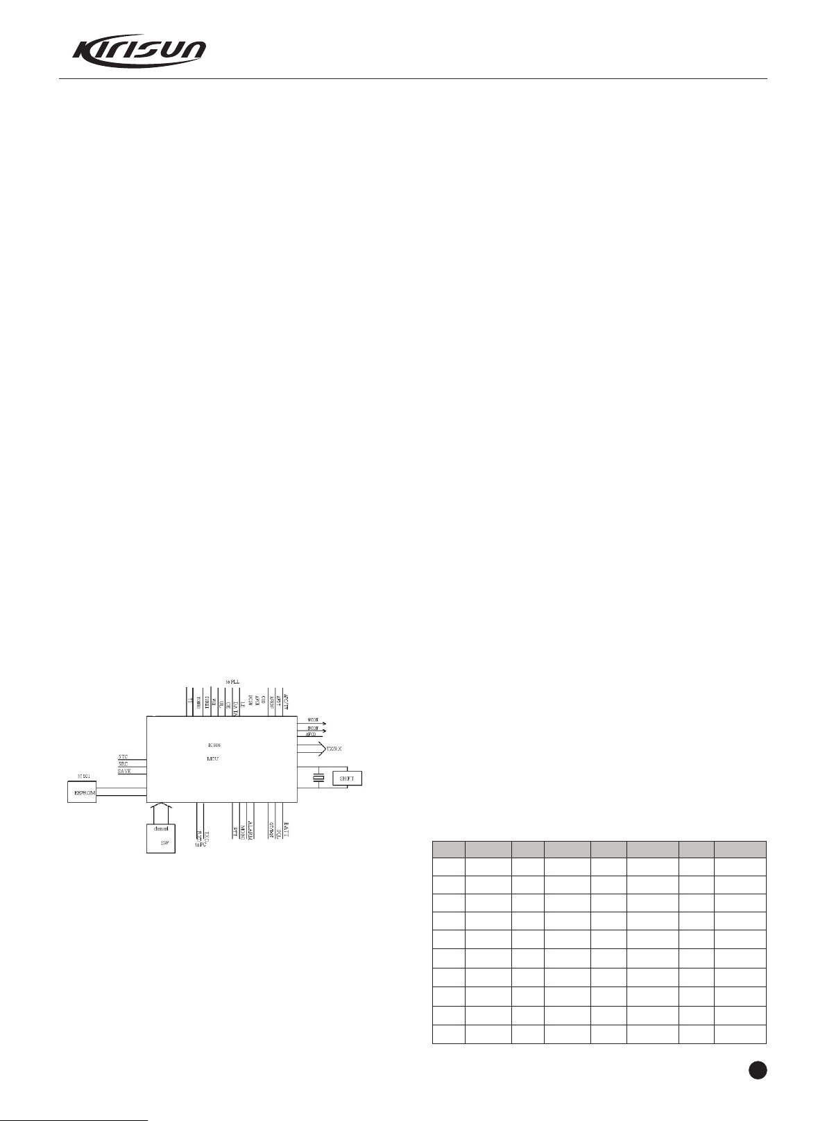
3.7 MCU
Checks the action of each function key
Generates content of voice indication
Generates Power-On Indication Tone
Generates CTCSS/DCS signals
Generates 2-Tone/5-Tone signals
Generates power control signals
CTCSS/DCS decoding
2-Tone/5-Tone decoding
Squelch check and control
Samplings VOX level
Controls audio processor to conduct audio emphasis/de-emphasis,
scrambler/descrambler, compander, filter and amplification.
Memorizer (E PROM,AT24C64)
Memorizes the radio channel data, CTCSS/DCS data, and other
data of function setting and parameter adjustment.
CTCSS/DCS Encoding and Decoding
CTCSS/DCS signals generated by MCU (output form pin20 and
pin26, PWM wave) are filtered at the filter circuit and then sent to
VCO and TCXO for modulation.
CTCSS/DCS signals from the receiver are sent to MCU for
demodulation. MCU determines whether the signals contain the
same CTCSS/DCS as that set on the radio and decides whether to
turn on the speaker.
Power Adjustment
MCU PIN2 sends DC signals to APC to control the transmitter
output power.
CTCSS
CTCSS (continuous tone control squelch system) is a squelch
control system modulated on carrier wave with continuous subaudio
frequency as pilot frequency. If a channel is set with CTCSS, only
when both the CTCSS of the receiver and that of the transmitter are
identical, communication is available, which avoids interference of
other signals.
2
Figure 3.11 MCU Diagram
MCU controls the working of each location of the radio to realize all
the radio functions.
Connects with the PC
Accesses the radio status data
Controls PLL to generate the receiving and transmitting local
oscillation frequency.
Accesses the current channel status.
Controls the LED status indication
Controls the power supply of each location
39 groups of standard CTCSS frequency is available on the radio,
see Table 3.1.
CTCSS signals generated by MCU (PWM wave) pass the low pass
filter consisting of RC to be filtered off the high frequency over
300Hz and then are sent to VCO for modulation.
No. Fr q [Hz] No. Frq [Hz] No. Frq [Hz] No. Frq[Hz]
1 67.0 11 94.8 21 131.8 31
2 69.3 12 97.4 22 136.5 32
3 71.9 13 100.0 23 141.3 33
4 74.4 14 103.5 24 146.2 34
5 77.0 15 107.2 25 151.4 35
6 79.7 16 110.9 26 156.7 36
7 82.5 17 114.8 27 162.2 37
8 85.4 18 118.8 28 167.9 38
9 88.5 19 123.0 29 173.8 39
10 91.5 20 127.3 30 179.9
186.2
192.8
203.5
210.7
218.1
225.7
233.6
241.8
250.3
5
Page 7
PT5200 SERVICE MANUAL
DCS
DCS (digital code squelch) is a kind of continuous digital code
modulated with voice signals on carrier wave to control squelch.
83 groups of standard codes (positive and inverse code) are
available. See table 3.2.
DCS signals generated by MCU (PWM wave shape) pass the low
pass filter to be filtered off the high frequency over 300Hz and then
are sent to VCO and TCXO for modulation. VCO modulates the
high frequency of DCS signals; TCXO modulates the low frequency
of DCS signals.
CTCSS/DCS signals from the receiver are sent to MCU for
modulation. MCU determines whether the DCS encoding of the
receiving signals is identical with that set on the radio and decides
whether to turn on the speaker.
Table 3.2 DCS Encoding List
023 114 174 315 445 631
025 115 205 331 464 632
026 116 223 343 465 654
031 125 226 346 466 662
032 131 243 351 503 664
043 132 244 364 506 703
047 134 245 365 516 712
051 143 251 371 532 723
054 152 261 411 546 731
065 155 263 412 565 732
071 156 265 413 606 734
072 162 271 423 612 743
073 165 306 431 624 754
074 172 311 432 627
3.9 Semiconductor Component
MCU Description
Table 3.3 Microprocessor (M30620FCPFP) Port Description
PIN
1
2
3
4
5
6
7
8
9
10
11
12
13
14
15
16
17
18
Port Name
TONEO
APC/TV
AFMUTE
SHIFT
SAVE
BYTE
CNVSS
XCIN
COUT
RESET
XOUT
GND
XIN
VCC
NMI
AFRDF
AFDT
TCLCK
I/O
Function
O
2T/5T output,warning tone output
O
TX power/ RX sensitivity adjustment
voltage output
O
RX audio mute control output, H: audio
output; L: mute
O
Frequency shift selection control
O
Control Power Save mode output
I
To select the width of the external data
bus, high level is 8-digit width.
I
working mode switching control
I
Backup clock input
O
Backup clock output
I
Reset input
O
Clock output
I
Ground
I
Clock input
I
Power positive polarity input
I
I
AK2346 RDF input
O
AK2346 TATA output
I
AK2346 MSK clock
19
20
21
22
23
24
25
26
27
28
29
30
31
32
33
34
35
36
37
38
39
40
41
42
43
44
45
46
47
48
49
50
51
52
53
54
55
56
57
58
59
60
61
62
63
64
65
66
67
68
69
70
71
72
73
74
75
CODIO
CTCOUT
PS
NC
NC
NC
NC
CTC_PLL
TONE1
NC
TXD
RXD
CLK1
RTSI
EECLK
EEDAT
NC
NC
NC
NC
NC
NC
NC
NC
NC
WE
NC
NC
NC
NC
NC
EEPROMR/W
NC
W588C
SCLK588
ADA588
BUSY588
NC
T/R
R5C
PLLUS
VCC
T5C
GND
MICMUTE
PLLDAT
PLLCLK
LE
TK
PTT
SK1
SK2
NC
NC
INT
NC
WCON
AK2346 DIO input
I/O
QT/DQT output
O
PLL power save mode control
O
NC
NC
NC
NC
NC
NC
NC
NC
QT/DQT PLL modulation output
O
2T/5T input test
I
NC
NC
Serial port output
O
Serial port input
I
NC
I
NC
O
EEPROM clock wire
I
EEPROM data wire
O
NC
NC
NC
NC
NC
NC
NC
NC
NC
NC
NC
NC
NC
NC
NC
NC
NC
NC
MCU read & write control
I
NC
NC
NC
NC
NC
O
NC
O
NC
O
EEPROM read & write enable
I/O
NC
NC
W588 audio chip control
W588 clock
W58 data
W58 test
NC
TX/RX VCO switching control. H: RX,
L:TX
R5V voltage control. L:R5V output
Unlock check,H:Lock,L: Unlock
I
5V voltage input
I
T5V voltage control. L:T5V output
O
GND
I
MIC mute control。L: mute
O
PLL data output
O
PLL clock output
O
PLL enabling output
O
Key check
I
PTT check
I
Key check
I
Key check
I
NC
O
NC
O
Low voltage check
NC
I
Wide band RX control. H:effective in wide
O
band
6
Page 8
PT5200 SERVICE MANUAL
76
77
78
79
80
81
82
83
84
85
86
87
88
89
90
91
92
93
94
95
96
97
98
99
100
NCON
LEDR
LEDG
NC
NC
AFCO
AFSCK
EN4
EN3
EN2
EN1
NC
NC
NC
TI
RSSI
BATT
VOX
GND
SQL
VCC
VCC
AFDIR
APCSW
DCSW
Narrow band RX control. H:effective in narrow
I
band
RX indicator control. H:Light
O
TX indicator control. H:Light
O
NC
I
NC
O
Audio power amplifier control. L: power
O
amplifier working
AK2346 data input/output clock
O
Channel encoding input (channel selection)
I
Channel encoding input (channel selection)
I
Channel encoding input (channel selection)
I
Channel encoding input (channel selection)
I
NC
I
NC
I
NC
I
CTCSS/DCS input
I
RX field strength signal input
I
Battery voltage check input
I
VOX voltage check input
I
GND
I
Squelch voltage check input
I
5V voltage input
I
5V voltage input
I
AK2346 data input/output control pin
O
TX power adjustment voltage input control
O
switch. H:Control is effective
TX power output control. L: TX power output
O
enabling
3.4 Semiconductor Function Description
Q503
Q502
Q504
Q405
Q404
2SJ243
2SA1745
2SJ243
DTC144EE
2SK1824
C5V switch
T5V witch
R5V switch
Receiver audio output switch, cut off
when in emergency mode.
Receiver audio output switch.
Table 3.5 Diode Function Description
Position
D102
D101
D103
D104
D201
D302
D304
D305
D310
D308
ZD101
D311
D306
D299
D508
D509
D505
D506
Type
MA77
HSC277
HSC277
HSC277
HSC277
MA2S376
MA2S376
MA360
MA2S376
MA2S376
HZU5ALL
MA2S111
MA2S111
1N4148
LED Red
LED Green
LED Red
LED Green
Function Description
Transmitter antenna switch diode
VCO output switch
Antenna switch
Antenna switch
VCO output switch
VCO oscillation variable capacitance diode
VCO oscillation variable capacitance diode
VCO modulation diode
VCO oscillation variable capacitance diode
VCO oscillation variable capacitance diode
APC output voltage-limiting diode
Loss of lock check diode
VCO power filtering accelerating diode
Noise demodulation
Transmitting indication
Receiving Indication
Transmitting indication
Receiving Indication
Table3.6:XF 203 Crystal Filter Features
Position
IC301
IC101
Ic204
IC408
IC402
IC401
Ic9
IC10
IC505
Q101
Q102
Q304
Q111
Q306
Q205
Q10
Q104
Q103
Q107
Q21
Q26
Q204
Q507
Q06
Type
MB15E03SL
NJM2904
Ta31136
AK2346
TC75W51FU
TDA2822D
AT2432NI
M30620FCPFP
R3111N45IC
2SC5108
2SC3356
2SC5108
2SC5108
2SC4617
2SC2412K
2SC1623
RD07MVS1
RD01MUS1
DTA144EE
3SK318
3SK318
2SC5108
DTC144EE
DTC144EE
Function Description
Frequency synthesizer
APC, voltage comparison, drive
Receiver's 2nd local oscillation, 2nd IF
a m p l if i c a ti o n , a mp l i t u de l i m i t ,
demodulation, noise amplification
Audio processing
MIC amplification
Receiver audio power amplifier
2
E PROM, memory channel frequency
data, function se t t i n g p a r a m e t e r,
debugging state parameters
MCU
MCU reset circuit
Transmitter 1st amplification
Transmitter 2nd amplification
VCO buffering amplifier
VCO buffering amplifier
VCO power filter
Noise amplifier
5V regulated output current stretcher
Transmitter final power amplifier
Transmitter power amplifier drive
APC output switch
The 1st frequency mixer
Receiver HF amplifier
The 1st IF amplifier
Red LED drive
Green LED drive
Item
Nominal center frequency
Transmission bandwidth
40dB barrage bandwidth
Pulse
Insertion loss
Guarantee attenuation
Terminal resistance
Specified Value
51.65MHz
±7.5kHz or bigger, within 3dB
±20.0kHz or smaller
1.0dB or smaller
3.0dB or smaller
80dB or bigger, within fo-910kHz
1.5kΩ/6PF
Table 3.7 CF201 LTWC450F Features
Item
Nominal center frequency
6Db bandwidth
50dB bandwidth
Pulse
Insertion loss
Guarantee attenuation
Specified Value
450kHz
±5.0kHz or bigger
±13.5kHz or smaller
3.0dB or smaller z
7.0dB or smaller
45.0dB or bigger, f0±100kHz
Table 3.8 CF202 LTWC450G Features
Item
Nominal center frequency
6Db bandwidth
50dB bandwidth
Pulse
Insertion loss
Guarantee attenuation
Specified Value
450kHz
±3.5kHz or bigger
±12kHz or smaller
3.0dB or smaller
7.0dB or smaller
45.0dB or bigger, f0±100kHz
7
Page 9
3SK318
M: YB-
G1
G2
D
S
G
S
D
CC
C
C
B
B
B
B
E
E
E
E
G
D
S
2SK1824
Mark: B1
2SC5108
M: MC
C
B
E
M: R24
2SC3356
C
B
E
2SC4617
C
B
E
C
B
E
2SC4738
KTC4082
C
B
E
2SC1623
M: L6
KTA1298
DTC144EE
M:16
GNDINOUT
HT7150-1
RD01MUS1
D
G
S
S
RD07MVS1
RDA0002
1
2
3
DA221
M: K
2SK308NV
DTA144EE
C
B
E
FMMT591
GSD
PT5200 SERVICE MANUAL
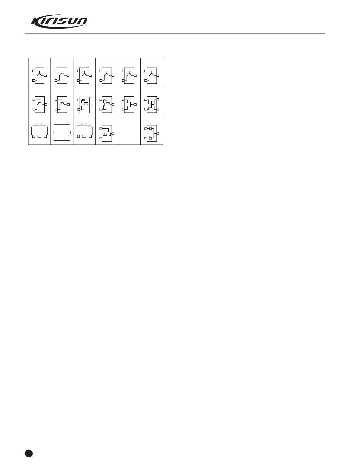
Figure 3.8 Semiconductor Component Packaging
Illustration:
Chapter 4 Function Description and Parameter
Setting
4.1 Major Functions
4.1.1 16 Channels
The radio stores 16 channels.
4.1.2 Scan Channel (programmable by PC software)
a) Press the key designated as “ Scan” to activate scanning.
While in scanning, the radio checks every channel and stops on the
channel on which a signal is detected until that signal disappears. If
the delay time between signal disappearing and continuing
scanning has been preset, the radio will remain on that channel in
the delay time even receiving any signals at that time.
Only when there are two channels added in the scan list and the
scan function has been activated, the radio can start scanning.
b) The dealer can set the revert channel (transmitting channel) in
scanning among the following options:
1) Selected: The radio always reverts to the channel selected
before scanning when pressing PTT.
2) Selected + Talk Back: When the radio is in scanning, press the
PTT button and the radio will transmit signals on the selected
channel.
When the radio is in scanning pause, press the PTT button and the
radio will transmit signals on the current talk back channel.
3)Priority: When pressing PTT, the radio will transmit signals on
the priority channel in the scanning list.
4) Priority + Talk Back: When the radio is in scanning, press the
PTT button and the radio will transmit signals on the priority
channel. When the radio is in scanning pause, press the PTT button
and the radio will transmit signals on the current talk back channel.
5) Last Called: When pressing PTT button, the radio will transmit
from the last channel that received a call. If it has never received
any calls, it will revert to the first channel in the scanning list.
6) Last Used: When pressing PTT button during the scanning, the
radio will transmit from the last channel that you used to transmit. If
it has never made any calls, it will revert to the first channel in the
scanning list
c) Priority Scan
During scanning, if the priority channel has been set on the radio,
8
when the priority channel receives a signal the radio will
automatically switch to the priority channel even the normal channel
is receiving signals at that time. And the radio will stay on the
priority channel till that signal disappears. The dealer can set the
delay time between signal disappearing and continuing scanning.
d) Temporarily Delete
When scanning pauses on a channel,channel, press and hold the
button programmed as “Temporarily Delete” or “Scan +
Temporarily Delete” for 1 second to delete this channel temporarily
from the scanning list.
Note: The priority channel cannot be deleted. And when the number
of scanning channels is less than 2, you cannot delete any channel,
either.
After exiting scanning mode and entering it again, the temporarily
deleted channel will be added in the scanning list again.
4.1.3 CTCSS/DCS
CTCSS/DCS can realize selective calls and group calls. On the
same channel, only the two parties whose CTCSS/DCS are
identical can communicate. CTCSS/DCS signaling code on the
channel is preset.
4.1.4 TOT
The purpose of the time-out timer is to prevent any single person
from overlong using a channel to transmit and affecting the whole
group communication.
If the radio transmits longer than the preset TOT time limit, the radio
will stop transmitting and warning tone sounds. To stop the warning
tone, release the PTT button. Press the PTT again you can resume
transmitting.
TOT Pre-Alert:
You can set the time when the radio generates a "Pre-Alert tone",
before the TOT (Time Out Timer) expires. TOT will expire when the
selected time passes after a “Pre-Alert Tone”.
TOT Rekey Time:
TOT Rekey-Time sets the "penalty" time in which the radio cannot
be re-keyed for transmitting after the Time Out Timer setting is
exceeded. During the Rekey time, if you press PTT, warning tone
sounds and transmission is prohibited.
TOT Reset Time:
TOT Reset Time sets the minimum "wait" time allowed between
transmissions that will reset the Time Out Timer. After setting this,
TOT continues even after PTT is released unless the TOT Reset
Timer has expired.
4.1.5 Auto Power Save
When no signals are being received or no operations are being
conducted for over 10 seconds, the battery power saving will be
activated to reduce power consumption. When it is receiving signals
or in operating state, battery power saving is inactive.
Power Save Type: 1:1, 1:2, 1:4, and OFF.
4.1.6 Low Battery Warning
When the battery power appears low, the indicator flashes. If the
battery power is lower than the preset value during transmitting, the
status indicator flashes red. When the speaker sounds warning
tone, the radio will stop transmitting.
Page 10

PT5200 SERVICE MANUAL
4.1.7 Monitor
When no signals are being received, the radio squelch circuit mutes
the speaker.
Press the MONI key to cut off the squelch control circuit, and you
will hear noise from speaker (no mater whether there are signals).
Such operation is very useful when you want to adjust voice volume
or receive weak signals (to avoid voice intermittence when in weak
signals).
When you press the MONI key, the green indicator lights, and the
radio is in the state of monitoring.
4.1.8 、 5-Tone Signaling
The dealer can activate or inactivate this function by programming.
5-Tone Signaling has 17 coding formats: CCIR1, CCIR2, PCCIR,
ZVEI1, ZVEI2, ZVEI3, PZVEI, DZVEI, PDZVEI, EEA, EURO
SIGNAL,NATEL, EIA, CCITT, MODAT, USER DEFINED1, and
USER DEFINED2. The last two are customized models.
1) 5-Tone Decoding
When receiving proper 5-tone signal, squelch will be activated
according to the “SP unmute” set by the user, and the radio can
receive the call and orange LED flashes.
The dealer can program the response way after decoding
succeeds.
2) 5-Tone Encoding:
If the PTT ID on the channel you select has been set with 5-Tone, 5Tone signal will be transmitted when making a call.
Or transmit 5-Tone signal by pressing the PTT button and CALL1 or
CALL2 button, which can be set by the dealer.
4.1.9、 2-Tone Signaling
The dealer can activate or inactivate this function by programming.
1) 2-Tone Decoding
When receiving proper 2-Tone signal, squelch will be activated
according to the “SP unmute” set by the user, and the radio can
receive the call and orange LED flashes.
The dealer can program the response way after decoding
succeeds.
2) 2-Tone Encoding:
If the PTT ID on the channel you select has been set with 2-Tone, 2Tone signal will be transmitted when making a call.
Or transmit 2-Tone signal by pressing the PTT button and CALL1 or
CALL2 button, which can be set by the dealer.
4.1.10、 PC Programmable
You can program the radio functions and adjust some parameters
by PC programming software KSP5200.
4.1.11、 Busy Channel Lockout
If “busy channel lockout” has been activated, transmitting signals
is prohibited on the busy channel. If you press the PTT to transmit
on the busy channel, the speaker will sound busy channel lockout
tone, and you cannot transmit signals.
The dealer can set one of the following BCL types:
1) OFF: BCL is inactive and you can transmit on the busy channel.
2) Carrier wave: If carrier wave is detected, the radio is unable to
transmit.
3) CTCSS/DCS: The radio is allowed to transmit when the
CTCSS/DCS signalings are identical.
4) Selective signaling: The radio is allowed to transmit when the
selective signalings (2-Tone or 5-Tone) are identical.
4.1.12 Squelch Level Selection
The purpose of the squelch is to mute the speaker noise when no
signals are received or the signals are weak. When the squelch is
activated, you can hear noise from the speaker; when the squelch
is inactivated, you will not hear noise form the speaker. Selecting
the squelch level is to select which the signal strength level is
strong enough to enable the squelch or weak enough to disable the
squelch. Over high squelch level will make the radio unable to
receive signals efficiently when signals are weak; over low squelch
level will make the radio communication affected by noise or other
irrelevant signals. The squelch level has 0-9 options.
4.1.13 Beep Tone
This option controls power on tone, channel busy tone and TOT
tone.
4.2 Parameter Setting (PC Mode)
The radio parameters have been programmed in the factory. The
user can program the radio parameters such as working frequency,
channels, CTCSS/DCS, auto scanning. We designed a user friendly
and convenient Chinese/English programming software KSP20 for
users to set parameters on the radio. The programming steps are
as follows:
A. Install the programming software KSP 5200 on the computer.
b. Connect the radio to the computer serial port with the specified
PC
programming line (KSPL02). See Figure 4.1
(RS232
Serial Port)
Programming
Line
(KSPL02)
Radio
(Speaker/ Mic
Socket)
Figure 4.1
C. Turn on the computer power.
D. Turn on the radio power.
E. Click the KSP5200 program to run the programming software.
F. Click the “Program” in the KSP5200 pull-down menu, and click
“Read from Radio” to read the radio parameters into the
computer; click “Write to Radio” to transfer the PC programming
parameters into the radio.
G. You can program the following parameters with the KSP5200
software.
1) The RX and TX frequency of each channel.
2) The receiving and transmitting signaling of each channel.
3) Busy channel lockout option.
4) TOT
5) Squelch level option.
6) 5-Tone
7) 2-Tone
8) Power saving option.
9) Beep tone option.
10) Monitor mode option.
11) Scan mode option.
12) Scan the revert channel option.
13) Scan the priority channel option.
For more details, please refer to the “Help” in the KSP5200
software.
Notice:
9
Page 11

PT5200 SERVICE MANUAL
1) Turn off the radio before connection.
2) When the radio is being read data, the indicator lights green and
it's prohibited to press the PTT button; when the radio is being
written data, the indicator lights red.
3) Before the first time editing, you should read data form the radio
and backup the data.
4) If the radio cannot work normally after being written in with the
editing data, open the data backup and rewrite the backup into the
radio.
5) Model information is important radio data and is prohibited to
modify.
6) After programming, you need to turn on the radio power again to
make the radio resume the normal work.
4.3 Computer Test Mode:
Connect the radio to the radio communication port with the
specified programming line (KSPL02). See Figure 4.1.
Warning: Before entering the computer test mode, connect a HF
load of 50Ωto the radio antenna connector or connect the radio to a
comprehensive test device.
Under the computer test mode, you can modify the following
parameters with KSP5200 programming software:
1) TX/RX low voltage
2) High/Medium/Low power
3) AK2346 VR 1/ 2 / 3 / 4
4) DCS (DQT) balance
5) DCS (DQT) frequency deviation
6) CTCSS (QT) frequency deviation
7) DTMF frequency deviation
8) Tone frequency deviation
9) MSK frequency deviation
10) VOX gaining
11) Sensitivity
12) SQL 1/9(OPEN/SQUELCH)
4.4 Wired Clone (It can be prohibited by programming
software)
When the wired clone function is activated, the radio can enter the
wired clone mode. After entering the wired clone mode, the radio
will not exit it automatically and you have to turn on the radio again
to enter the user's mode. Operating steps are as follows:
1) Turn on the radio with the MONI key pressed, and 2 seconds
later the red light flashes twice and two beep tones sound, and then
the radio enters the wired clone mode.
2) Press the PTT button on the host radio to activate/inactivate the
wired clone mode on the sub radio. But the wired clone mode of the
host radio will not be changed. When pressing the PTT button, the
green light flashing twice and one beep mean to activate the clone
mode on the sub radio; the red light flashing twice and two beeps
mean to inactivate the clone mode on the sub radio.
3) Press the MONI key, red light flashes, and it starts cloning. After
cloning is finished, the red light turns dim.
Chapter 5 Service Assemble and Disassemble
The radio is precision communication equipment. Please be careful
when assemble or disassemble the radio during service.
5.1 Removing and Installing the Battery
To remove the battery, push the latch upwards and remove the
battery away from the radio. (See Figure 5.1)
Figure 5.1
To install the battery, match the tow bulges at the bottom of the
battery with the corresponding grooves at the radio aluminum alloy
frame and insert it in. Then press the upper end of the battery till
the latch secure. (See Figure 5.2 and 5.3)
Figure 5.2 Figure 5.3
5.2 Removing and Installing the Belt Clip
To remove the belt clip, use your nail or a tool to lift the metal
spring piece in the belt clip from the topside, and then pull the belt
clip away from the radio.
To install the belt clip, match the upper head of the belt clip with the
glides on the rear of the battery, and then press the belt clip
downwards to lock it in place. (See Figure 5.4)
Note:
You can also activate/inactivate the wired clone mode by PC
Cloning Line
Host Radio
Figure 4.2
Sub Radio
10
Figure 5.4
Page 12

PT5200 SERVICE MANUAL
5.3 Removing the Casing from the Chassis
1) Remove the knobs;
2) Remove the two knob nuts and the antenna nut;
3) Remove the two cross head screws that fix the top cover at
the top;
4) Remove the two cross head screws that fix the aluminum
alloy frame at the bottom;
5) Pull the aluminum alloy frame out of the casing.
See Figure 5.5
Figure 5.5
5.4 Remove the Chassis from the Main Board
1) Remove the screw of from the PCB;
2) Melt the solder at the antenna point with an electric soldering
iron and take off the main board;
3) Take away the two screws and the antenna connector.
See Figure 5.6.
Figure 5.6.
5.4 Exploded View
No . MATE R AL No .I DECR IPT ION QTY
1
201- 000 668 -R0 4
2
201- 000 668 -R0 5
3
202- 000 668 -R0 1
203- 000 558 -R0 4
4
5
201- 005 200 -R0 1
6
121- 100 000 -R0 7
7
204- 000 558 -R0 1
8
201- 000 558 -R0 9
9
10
202- 000 558 -R0 5
11
202- 000 558 -R0 4
203- 000 558 -R0 1
12
13
203- 000 558 -R0 2
14
203- 003 208 -R0 9
15
201- 000 668 -R0 3
16
201- 000 668 -R0 2
17
202- 000 5
18
201- 000 558 -R0 8
19
202- 000 558 -R0 1
20
204- 006 800 -R0 6
21
202- 000 558 -R0 9
22
301- 200 40G -R0 1
23
204- 000 558 -R0 4
24
204- 003 208 -R0 5
25
202- 000 558 -R0 6
26
27
201- 000 558 -R0 7
28
202- 000 558 -R0 8
29
203- 003 208 -R0 2
30
302- 170 40G -R0 1
31
202- 003 208 -R0 7
32
202- 000 558 -R0 7
33
203- 000 558 -R0 7
34
204- 000 558 -R0 5
35
203- 004 200 -R0 1
36
203- 003 208 -R0 4
37
201- 000 558 -R0 5
38
203- 000 558 -R0 5
39
201- 000 558 -R0 6
40
301- 250 60J -R0 1
41
204- 000 558 -R0 2
42
401- 020 1C1 -R0 6
43
301- 200 80G -R0 1
44
204- 000 558 -R0 3
58-R 03
PTT CO VER B OAR D
PTT PL ASTIC KEYSTRO KE
PTT KE YSTROKE
SPEA KER S PRI NG
LOGO L ABL E
SURFA CE SH ELL
SPEA KER
WATERP RO OF WA SHER
LIGH T POLE
ANTE NNA WATE RPR OOF WAS HER
SWIT CH WATE RPR OOF WASHER
ANTE NNA NU T
SWIT CH NU T
KNOB R ETAINING RI NG
ENCO DER K NOB
VOLU ME KN OB
ANNU NCI ATO R KEY STR OKE
ANNU NCI ATO R KEY STR OKE STAK E
MIC CO VER
MIC WASH ER
MIC UN DER LAY
SCRE W M2
PCB SU BAS SEM BLY
WAS HER
WAS HER
WAS HER
ANOD E SHR APN EL BRAC KET
ANOD E CATHODE WA SHE R
ANOD E SHR APN EL
SCRE W M1. 7
INSU LATING WAS HER
WATERP ROO F WA SHE R
ANTE NNA HE AD
ALNI CO AEG IS PASTE R
ALNI CO BR ACK ET
CATHO DE SHRAPNEL
COPI NG
PUSH FA STE NER S PRI NG
PUSH FA STE NER
SCRE W M2. 5
WATERP ROO F WA SHE R
ALNI CO LA BLE
SCRE W M2
BUTT OM LABLE
1
1
1
2
1
1
1
2
1
1
2
1
2
2
1
1
1
1
1
3
1
10
1
2
2
1
1
2
1
1
1
1
1
1
1
1
1
1
1
2
1
1
2
1
11
Page 13

PT5200 SERVICE MANUAL
0
4
39
8
3
37
36
35
34
3
3
2
3
31
0
3
29
8
2
7
2
26
5
2
24
3
2
2
1
4
2
4
19
20
3
4
44
21
18
7
1
16
5
1
2
14
13
2
1
11
10
9
8
7
6
5
4
3
2
1
5. 6 Wearing Parts List
Material Serial No.
No .
111-030000-R03
1
110-220103-R12
2
106-ED0873-R01
3
124-050000-R05
4
124-050000-R04
5
604-052000-R01
6
202-000558-R01
7
202-000668-R01
8
201-000668-R05
9
201-000668-R04
10
604-006680-R02
11
604-006680-R03
12
203-000558-R11
13
203-000558-R02
14
204-003208-R05
15
202-000558-R04
16
202-000558-R05
17
203-000558-R07
18
19
20
202-000558-R09
21
301-20040G-R01
22
604-005580-R04
23
301-20080G-R02
24
604-005580-R05
25
301-25050J-R01
604-005580-R06
26
202-000558-R07
27
Name
Chip protective tube
Volume switch
Channel/Encoder switch
Earphone rod bearing
MIC rod bearing
PT5200 front cover components
PT558 earphone/Mic cover
PT668PTT rubber key
PT668PTT key
PT668PTT cover
PT668 Volume knob module
PT668Channel knob module
PT558 Antenna knob
PT558 Switch knob
PT3208 Potention meterention
meter washer
PT558 switch waterproof gasket
PT558 antenna waterproof gasket
PT558 antenna connector
PT5200 electrical material
PT558 MIC cover
M2.0*4.0 Woven belly-tooth screw
PT558 Positive pole terminal module
M2.0*8.0 Woven belly-tooth screw
PT558 Al alloy chassis
M2.5*5.0 Woven belly-tooth screw
PT558 Top cover module
PT558 Large waterproof gasket
Figure 5.7 Exploded View
QTY
FS01
K501
K502
J401
J402
1
1
1
1
1
1
1
1
2
2
2
1
1
1
1
10
1
2
1
2
1
1
28
29
30
31
32
33
34
35
36
37
38
39
40
41
42
43
44
45
46
47
48
49
50
51
121-100000-R07
201-000558-R08
201-000558-R09
201-005200-R02
202-000558-R03
204-000558-R01
204-006800-R06
201-000668-R03
203-003208-R09
201-000558-R07
202-000558-R06
202-000558-R08
203-003208-R02
302-17040G-R01
202-000558-R08
203-003208-R04
203-004200-R01
204-000558-R02
204-000558-R03
204-000558-R05
301-20030G-R03
201-000558-R05
202-000558-R14
203-000558-R05
Speaker
PT558 Emergency Key Panel
PT558 Light guide lens
PT5200 Front cover
PT558 Emergency Key
PT558 Speaker waterproof net
PT6800 MIC gasket
PT668 Channel knob
PT3208 Knob retaining ring
PT 5 5 8 P o s itiv e po le ter m i nal
chassis
PT558 chassis waterproof gasket
PT558 Positive pole terminal gasket
PT558 Positive pole terminal
Screw
PT 5 5 8 Posit i v e /Ne g a t ive po l e
terminal gasket
PT3208 Negative pole terminal
PT4200 Al alloy chassis
PT558 waterproof spacer
PT558 Al alloy sticker
PT558 Al alloy spacer
Screw
PT558 Top cover
PT558 Push fastener
PT558 Push fastener spring
1
1
1
1
1
1
3
1
1
1
1
1
1
1
1
1
1
1
1
1
1
1
1
1
12
Page 14

MIC JACK
SPEAKER JACK
PTT/RXD
MIC
5MS
GND
TXD
SP
PT5200 SERVICE MANUAL
Chapter 6 Radio Debugging
Before test/debugging, make sure all the equipments have been
well connected to the ground.
Before test/debugging, make sure the antenna output terminal has
been connected properly to the corresponding devices and load.
The transmitter output must pass RF power attenuator before being
connected to the standard signal source/ frequency deviator/
frequency spectrum.
When testing the receiver, make sure not to conduct transmitting
operation.
When in debugging/testing/service, make sure static free measures
for human body and equipments.
6.1 Service Equipment and Software.
The following equipments and software in Table 6.1 are necessary
for the service and test of the radio.
Table 6.1 For Test and Service: Equipment and Software
No.
Item
1
Computer
2
Programming
Software
3
Programming Line
4
Cloning Line
5
DC Regulated
Power
6
RF power meter
7
Frequency Meter
8
Frequency
Deviator
9
Digital Multimeter
10
Audio Signal
Generator
11
RF power
Attenuator
12
Standard signal
source
13
Oscillograph
14
Audio voltmeter
The equipments in item 6, 7, 8, 10, 11, and 12 can be replaced by a
comprehensive test instrument.
Specifications
Higher than P2, compatible with IBM PC,
WINDOWS 98/ME/2000/XP
KSP-5200
KSPL02
KCL01
Output voltage:7.5V, Output current:≥ 5A
Test range:0.5---10W
Frequency range:100MHz500MHz
Impedance:50Ω
SWR≤1.2
Frequency range: 0.1600MHz
Frequency precision: Higher than ± 1×10
Sensitivity: Higher than 100mV
Frequency range:DC600MHz
Test range:0--±5kHz
Input impedance:Higher than 10MΩ/V DC , with
the ability of testing voltage, current, impedance.
Frequency range: 2---3000Hz
Output level: 1---500mV
Attenuation:40dB or 50dB
Supporting power:Bigger than 10W
Frequency range:10MHz---1000MHz
Output level:0.1uV~32mV (-127dBm~-17dBm)
Frequency range: DC~20MHz
Test range:10mV~20V
Test range:10mV~10V
-6
6.2 Debugging Items
During the course of maintenance, the radio needs to be tested and
debugged after replacing components. Some certain radio
parameters can be modified (computer mode) with our KSP 5200
programming software. The modifiable parameters are as follows:
1) Frequency difference
2) TX power
3) Low battery power warning threshold
4) Squelch level
5) CTCSS (QT) frequency deviation
6) DCS (DQT) frequency deviation
7) TX frequency deviation
8) DTMF frequency deviation
9) TONE frequency deviation
10) RX sensitivity
11) RX AF power
Debugging Procedures
a. Enter the computer test mode. Access method refers to the
instruction in 4.2.1 parameter setting.
b. Select the “Test Mode” option is KSP5200 program to
enter the computer test mode.
c. Select the options that you want to adjust and adjust the
parameters on the computer.
d. After adjustment, exit the computer test mode.
6.3 Debugging
6.3.1 TX Low Power Warning
Adjust the voltage to 6.6V.
In “Test Mode” press “↓” to select “TX lower power” and
press Enter key.
6.3.2 VCO Modification
Turn off the power saving mode. Set the RX frequency at the low
frequency (see Table 6.2). In receiving status, test the PD power
with the digital multimeter. Adjust the trimming capacitor TC302 to
make the PD power at 1V±0.1V. Set the RX frequency at the high
frequency, and PD power is 3.5V±0.1V.
Set the TX frequency at low frequency (see Table 6.2), press the
PTT button, test the PD power with the digital multimeter. Adjust the
trimming capacitor TC301 to make the PD power at 1V±0.1V. Set
the TX frequency at the high frequency, and PD power is 3.5V±
0.1V.
Table 6.2 Radio H/I/L Frequency
Low Frequency Medium Frequency High Frequency
TX 420.165MHz 445.165MHz 469.965MHz
RX 420.165MHz 445.165MHz 469.965MHz
Figure 6.1 External Speaker/Mic Connector Definition
6.3.3 PLL Frequency Adjustment
Under the computer test mode, press “ ”on the keyboard to
↓
enter “Low Power (Low)” and press Enter. Adjust VR1 to make
the TX frequency error at +/-200HZ.
6.3.4 TX Frequency Adjustment
Under the computer test mode, press “↓”on the keyboard to
enter “Low Power (Low)” and press Enter. Press “←/→”key to
make the TX power at 0.5+/-0.1w and then press Enter to store the
setting. Use the same way to adjust “Low Power (Medium), Low
Power (Medium High), Low Power (High)” at 0.5+/-0.1w.
13
Page 15

Press “ ”on the keyboard to enter “Medium Power (Low)”
and press Enter. Press “←/→”key to make the TX power at 2+/-
0.2w and then press Enter to store the setting. Use the same way to
adjust “Medium Power (Medium), Medium Power (Medium High),
Medium Power (High)” at 2+/-0.2w.
Press “↓”on the keyboard to enter “High Power (Low)” and
press Enter. Press “←/→”key to make the TX power at 4+/-0.3w
and then press Enter to store the setting. Use the same way to
adjust “High Power (Medium), High Power (Medium High), High
Power (High)” at 4+/-0.3w.
6.3.5 Frequency Deviation Adjustment
Input 150mV, 1000Hz audio signals from the radio MIC, and press
“↓”to enter “AK2346 VR2 Wide Band Low” and press Enter.
Press “←/→”key to make the maximum frequency deviation at
3.9+/-0.2KHZ.
Use the same way to make the maximum frequency deviation of “
AK2346 VR2 Wide Band Medium”, “AK2346 VR2 Wide Band
High” at 3.9+/-0.2KHZ; “ AK2346 VR2 Medium Band Medium”
at 3.2+/-0.1KHZ; “AK2346 VR2 Narrow Band Medium” at 2.0+/-
0.2KHZ. (Notice: On the comprehensive test device, the audio
output level is 150mv and the filter is set to 50HZ~15K.)
6.3.6 DCS (DQT) TX Signal Wave Shape and Frequency
Adjustment
Under the computer test mode, press “↓”on the keyboard to
enter “DCS Frequency Deviation (Wide, Low)” and press Enter.
Press “←/→”key to make the DCS Frequency Deviation at
0.85+/-0.15KHZ. Use the same way to adjust “DCS Frequency
Deviation (Wide, Medium)” “DCS Frequency Deviation (Wide,
High)” at 0.80+/-0.10KHz; “DCS Frequency Deviation (Medium,
Medium)” at 0.6+/-0.1KHz; “DCS Frequency Deviation (Narrow,
Medium)” at 0.4+/-0.1KHz. (Notice: The filter is set to
20HZ~300HZ.)
6.3.7 CTCSS (QT) Frequency Deviation Adjustment
Under the computer test mode, press “↓”on the keyboard to
enter “CTC Frequency Deviation (67.0HZ ,Wide, Low)” and
press Enter. Press “←/→”key to make the CTC Frequency
Deviation at 0.80+/-0.10KHZ. Use the same way to adjust “CTC
Frequency Deviation (67.HZ ,Wide, Medium)”, “CTC Frequency
Deviation (67.HZ, Wide, High)” at 0.80+/-0.10KHZ; “CTC
Frequency Deviation (67.0HZ, Medium, Medium)” at 0.6+/-
0.1KHZ; “CTC Frequency Deviation (67.0HZ, Narrow, Medium)”
at 0.4+/-0.1KHZ; the test and specifications are the same for “CTC
Frequency Deviation (136.5HZ) and ”CTC Frequency Deviation
(254.1HZ). (Notice: The filter is set to 20HZ~300HZ.)
6.3.8 DTMF Frequency Deviation Adjustment
Under the computer test mode, press “↓”on the keyboard to
enter “DTMF Frequency Deviation (Wide Band)” and press
Enter. Press “←/→”key to make the DTMF Frequency Deviation
at 3+/-0.3KHZ.
Press “↓”on the keyboard to enter “DTMF Frequency
Deviation (Medium Band)” and press Enter. Press “←/→”key to
make the DTMF Frequency Deviation at 2.3+/-0.2KHZ.
Press “↓”on the keyboard to enter “DTMF Frequency
↓
PT5200 SERVICE MANUAL
Deviation (Narrow Band)” and press Enter. Press “←/→”key to
make the DTMF Frequency Deviation at 1.5+/-0.1KHZ.
6.3.9 TONE Frequency Deviation Adjustment
Under the computer test mode, press “↓”on the keyboard to
enter “TONE Frequency Deviation (Wide Band)” and press
Enter. Press “←/→”key to make the TONE Frequency Deviation
at 3+/-0.3KHZ.
Press “↓”on the keyboard to enter “TONE Frequency
Deviation (Medium Band)” and press Enter. Press “←/→”key to
make the TONE Frequency Deviation at 2.3+/-0.2KHZ.
Press “↓”on the keyboard to enter “TONE Frequency
Deviation (Narrow Band)” and press Enter. Press “←/→”key to
make the TONE Frequency Deviation at 1.5+/-0.1KHZ.
6.3.10 VOX Gain Debugging
Under the computer test mode, press “↓”on the keyboard to
enter “VOX Gain 5 (Medium)” (set the output level on the
comprehensive test device to 15mv) and press Enter to store the
data ----- do not press Enter until the numbers on the screen
become steady.
Press “↓”on the keyboard to enter “VOX Gain 1 (Medium)”
(set the output level on the comprehensive test device to 100mv)
and press Enter. Do not press Enter to store the data until the
numbers on the screen become steady.
6.3.11 Receiver Sensitivity
Under the computer test mode, set the comprehensive test device
at the sate of testing pass band, and press “↓”on the keyboard
to enter “Receiver Sensitivity (Low)” and press Enter. Press “←
/→”key to make the frequency waveform to the middle of the
whole waveform. Then press Enter to store the data. It's the same
to other 4 testing points (notice the corresponding frequency
change).
6.3.12 AK2346 Receiving Voice Debugging
Under the computer test mode, set the RX frequency on the
comprehensive test device to the middle frequency among the 5
testing frequency points; signal strength at 1mv; AF voltage unit is
“W”.
Press “↓”on the keyboard to enter “AK2346 VR3 (Wide Band,
Medium)” and press Enter. Press “←/→”key to make the AF
power to 0.4+/-0.05W. Set the AF power of “AK2346 VR3 (Medium
Band, Medium)” and “AK2346 VR3 (Narrow Band, Medium)” to
0.4+/-0.05W. (On the comprehensive test device, the AF deviation
is 3KHZ, 2.5KHZ, and 1.5KHZ separately.)
6.3.13 Receiver Squelch Setting
Under the computer test mode, press “↓”on the keyboard to
enter “SQL 1 ON (Wide Band, Low)” (on the comprehensive test
device the RX frequency is low frequency, SIAND is adjusted to
10dB). Press Enter to watch the RX sensitivity and press Enter to
store the data after the value becomes steady. It's the same for
“SQL 1 ON (Wide Band, Medium Low)”, “SQL 1 ON (Wide
Band, Medium)”, “SQL 1 ON (Wide Band, Medium High)”, and
“SQL 1 ON (Wide Band, High)”. (On the comprehensive test
device, the AF deviation is 3KHZ, 2.4KHZ, and 1.5KHZ separately.)
Press “↓”on the keyboard to enter “SQL 1 OFF (Wide Band,
Low)” (on the comprehensive test device the RX frequency is low
14
Page 16

PT5200 SERVICE MANUAL
frequency, SIAND is adjusted to 8dB. Press Enter to watch the RX
sensitivity and press Enter to store the data after the value
becomes steady. It's the same for “SQL 1 OFF (Wide Band,
Medium Low)”, “SQL 1 OFF (Wide Band, Medium)”, “SQL 1
OFF (Wide Band, Medium High)”, and “SQL 1 OFF (Wide Band,
High)”.
Press “↓”on the keyboard to enter“SQL 9 ON (Wide Band,
Low)” (on the comprehensive test device the RX frequency is low
frequency, SIAND is adjusted to -117dB). Press Enter to watch the
RX sensitivity and press Enter to store the data after the value
becomes steady. It's the same for “SQL 9 ON (Wide Band,
Medium Low)”, “SQL 9 ON (Wide Band, Medium)”, “SQL 9
ON (Wide Band, Medium High)”, “SQL 9 ON (Wide Band,
High)”, “SQL 9 OFF (Medium Band, Medium)” and “SQL 9
OFF (Narrow Band, Medium)”.
Press “↓”on the keyboard to enter “SQL 9 OFF (Wide Band,
Low)” (on the comprehensive test device the RX frequency is low
frequency, SIAND is adjusted to -119dB. Press Enter to watch the
RX sensitivity and press Enter to store the data after the value
becomes steady. It's the same for “SQL 9 OFF (Wide Band,
Medium Low)”, “SQL 9 OFF (Wide Band, Medium”, “SQL 9
OFF (Wide Band, Medium High)”, “SQL 9 OFF (Wide Band,
High)”, “SQL 9 OFF (Medium Band, Medium)” and “SQL 9
OFF (Narrow Band, Medium)”.
Chapter 7 Technical Specifications
7.1 General Specification
Frequency( )
Modulation
Number of Channels
Channel Spacing
MF
Working Voltage
Working Temperature
Antenna Impetance
Mic Impedance
Battery (Standard)
Dimension (WxHxD)
Weight
7.2 Receiver
Available Sensitivity (12dB SINAD)
Squelch Activation Sensitivity
Receiver Surplus Output
Modulation Receiving Bandwidth
Adjacent Channel Selectivity
Intermediation Reject Ratio
Spurious Response Reject Ratio
Audio Output Power
Receiver Surplus Output
Modulation Receiving Bandwidth
MHz
136~174MHz 470~512 MHz
400~450MHz 350~390 MHz
420 ~ 470MHz
16K0F3E
16
25 kHz(W),20 (M),12.5 (N)
1st MF:51.65MHz 2nd MF:450kHz
7.5V negative grounding
-25℃~ +55℃
50Ω
2kΩ
Model:KB-58L,Li-Ion Battery DC 8.4V , 1200mAh
56 mm×102 mm×29 mm
235g(With battery and antenna)
kHz kHz
≤0.28μV
≤0.25uV @ level 3 squelch
≤-45dB
±7kHz
≥70dB
≥65dB
≥70dB
Internal speaker:500mW,balance
@ distortion≤5%,16Ω
≤350mA
≤20mA
7.3 Transmitter
RF Power
Frequency Stability
Maximum Modulation Frequency
Deviation
Modulation Sensitivity
Modulation Distortion(300~3000Hz)
Adjacent Channel RF Power
Spurious and Harmonics
Residential Frequency
Modulation
Transmitting Current Sinking
4.0W @7.5V DC
±
≤ 2.5×10
±5kHz
15mV
≤ 3%
≤-70dB
≤ -70 dB
≤ -45 dB
≤1.8A @ 7.5V DC
-6
Chapter 8 Trouble Shooting
No display after
1
switching on the
radio.
PLL is
2
unlocked.
(Beep
sounds)
3
Cannot talk to
or hear other
group
members.
4
Cannot receive
signals.
5
The indicator
lights red when
in transmitting
but no voice
can be heard.
6
The indicator
lights green
when in
receiving but no
voice can be
heard.
7
Cannot
program the
radio
parameters
normally.
Battery power may be insufficient. Recharge or
change the battery pack.
The power switch is broken, and please change it.
The CPU is broken, and please change it.
The radio is remote killed and reprogram it.
The PLL crystal oscillator X301 is broken, and
please change it.
The oscillatingtube is broken, and please change
it.
The PLL chip IC301 is broken, and please change
it.
Make sure the two communication radios are
using the channel of the same frequency.
Make sure the CTCSS/DCS tone is the same as
that of your group members.
Out of the effective communication range.
The antenna is not well connected, and please
screw the antenna again until secure.
HF amplifier Q26 is broken, and please change it.
The squelch level is too high and the squelch
cannot be activated. Reset the squelch level with a
computer.
Mixer tube Q21 is broken, and please change it.
MF processing chip IC408 is broken, and please
change it.
The power amplifier tube Q104 is broken and
there is no power output and please change it with a
new tube.
The microphone is broken, and please change it
with a new one.
The operational amplifier IC402 is broken, and
please change it with a new one.
The speaker is broken, and please change it with
a new one.
The audio amplifier IC401 is broken and please
change it with a new one.
The switch tube Q404 and Q405 is broken, and
pleas change it with a new one.
The operational amplifier IC408 is broken, and
please change it with a new one.
Make sure the programming cable is well
connected.
The computer RS-232 serial port output is
unmoral, and please fix the computer.
The MIC is not well connected with the SPK
socket. Check the socket and if it is unable to work
normally please change it with a new one.
15
Page 17

PT5200 SERVICE MANUAL
Chapter 9 KBC-42A Charger
9.1 Charger Specifications
A) Idling Input Current: ≤15mA
B) Charging Terminal Maximum Idling Voltage: 96%~97% of the
Input voltage
C) Ni-MH Battery's Maximum Charging Time : 285±15 seconds
D) Lithium Battery's Maximum Charging Time: 510±30 seconds
E) Maximum Charging Voltage Limit: 9.4V±0.1V
9.2 Charging and Charging Indicator
Charger Status
Standby/ No
Connection with
Battery
Precharge
Rapid Charge
Complete Charging or
in Trick Charge
Output Short-circuit
Abnormal
LED Status
Charging Power Indicator Battery Temperature
Indicator Abnormal Indicator
(RED) GREEN (YELLOW)
/ Light /
Flash / /
Light / /
/ Light (Ni-MH) /
/ / /
/ / Light
( )
Appendix 1 Abbreviations
AMP amplify, amplifier
ANT antenna
APC automatic power control
BPF band pass filter
CTCSS continuous tone control squelch system
DCS digital code squelch
DEMOD demodulation
2
E PROM electrically erasable programmable read-only memory
HPF high pass filter
IDC instantaneous deviation control
IF intermediate frequency
LED Light-Emitting Diode
LNA low noise amplifier
LPF low pass filter
MCU micro control unit
MIC microphone
MOD modulation
MONI monitor
PLL phase lock loop
PTT push-to-talk
RX receiver
SPK speaker
TCXO temperature compensated crystal oscillators
TX transmitter
UL un-lock
VCO voltage control oscillator
LED red: Charging indication
LED yellow: Power indication
LED green: Charging completion
Note:
After putting the battery pack that has been discharged completely
into the charger, its red indicator needs about 1~2 minutes to turn
light.
16
Appendix 2 Framework Component List
No. Material Serial No. Name/Specification Note QTY
1
201-005200-R04
2
201-000668-R02
3
201-000668-R03
4
201-000668-R04
5
201-000668-R05
6
201-000558-R05
7
201-000558-R14
8
201-000558-R07
9
201-000558-R08
10
201-000558-R09
11
203-000558-R07
12
203-000558-R11
13
203-000558-R02
14
203-003208-R09
15
203-003208-R02
16
203-003208-R04
17
203-004200-R01
18
203-000558-R04
19
203-000558-R05
Surface shell,PC+ABS, black
Volume knob,PC+ABS,black
Encoder knob,PC+ABS,black
PTTcover board,PC+ABS,black
PTT plastic
keystroke,PC+ABS,black
Coping,PC+ABS,black
Push fastener,PC+ABS,black
Anode shrapnel
bracket,PC+ABS,black
Annunciator keystroke
stake,PC+ABS,black
Light pole,PMMA,transparent
Antenna head, brass nickle
plating
Antenna nut,brass,black
passivation
Switch nut,brass,black
passivation
Knob retaining ring,stainless
steel,0.18THK
Anode shrapnel, phosphorus
copper gold plating
Cathode shrapnel, phosphorus
copper gold plating
Alnico bracket
Speaker contact spring,carbon
spring steel wire ∮0.25,gilt
Push fastener spring,carbon
spring steel wire ∮0.35,nickle
plating
2 nuts inlaid
Refer to
PT3208
Refer to
PT3208
Refer to
PT3208
1
1
1
1
1
1
1
1
1
1
1
1
2
2
1
1
1
2
1
Page 18

PT5200 SERVICE MANUAL
No. Material Serial No. Name/Specification Position Note QTY
20
202-000558-R01
21
202-000668-R01
22
202-000558-R03
23
202-000558-R04
24
202-000558-R05
25
202-000558-R06
26
202-000558-R07
27
202-000558-R08
28
202-000558-R09
29
204-000558-R01
30
204-006800-R06
31
204-000558-R02
32
204-000558-R03
33
204-000558-R04
34
202-003208-R07
35
302-17040G-R01
36
301-20040G-R01
37
301-20080G-R02
38
301-25050J-R01
Earpiece-Mic jack panel cover black silica gel(enhanced elasticity)
hardness70
PTT keystroke black silica gel(enhanced elasticity)
Annunciator keystroke orange silica gel(enhanced elasticity) hardness60
Switch water-proof gasket black silica gel hardness60
Antenna water-proof gasket black silica gel hardness60
Waterproof gasket black silica gel hardness60
Waterproof gasket black silica gel(enhanced elasticity) hardness40
Negative & positive terminal cushion black silica gel hardness40
Mic case orange silica gel hardness40
Speaker waterproof net,black waterproof cloth
Mic cushion,dustproof net black
Waterproof spacer PORON black self-adhesice 0.8THK
Aluminium alloy sticker 1 PVC black self-adhesice 0.3THK
Potentionmeter cushion PVC transparent self-adhesive 0.35THK
Thermally conductive insulator,thermally conductive rubber,2*6*9 blue
Self-tapping screw,M1.7X4.0 flat round cross head nickle plating
Woven belly-tooth screw,M2.0X4.0 flat round cross head, nickle plating
Woven belly-tooth screw,M2.0X8.0 flat round cross head,nickle plating
Woven belly-tooth screw,M2.5X5.0 flat round cross head,nickle plating
Appendix 3 Electronic Component List
Refer to PT6800
Refer to PT3208
Refer to PT3208
Refer to PT3208
Under FET
Positive terminal screw
PCB,antenna head,negative terminal
screw
terminal screw
Alnico bracket fixing coping fixing
1
1
1
2
1
1
1
2
1
1
3
1
1
1
1
1
10
2
2
No. Material Serial No. Name/Specification QTY
1
101-05200U-R03
2
102-5VL45C-R01
3
102-9140NR-R01
4
102-A31136-R01
5
102-AK2346-R01
6
102-B15E03-R01
7
102-C75W51-R01
8
102-DA2822-R01
9
102-FP3502-R01
10
102-K11250-R01
11
102-M2904V-R01
12
102-M30620-R01
13
102-P502PR-R01
14
102-T24C64-R01
15
103-00MA77-R01
16
103-0MA742-R01
17
103-1SR154-R01
18
103-1SS373-R01
19
103-1SV278-R01
20
103-A2S077-R01
21
103-A2S111-R01
22
103-DAN222-R01
23
103-HVC350-R01
24
103-HVC376-R01
25
103-L190YG-R01
26
103-MHC190-R02
27
103-RB706F-R01
28
103-Z80680-R01
29
104-00UMC4-R01
30
104-A144EE-R01
31
104-C114EE-R01
32
104-C144EE-R01
33
104-SA1745-R01
34
104-SC2412-R01
35
104-SC3356-R01
36
104-SC4116-R01
37
104-SC4617-R01
38
104-SC5108-R01
PT5200PCB / PT5200U-070110.PCB,
ResetIC / R3111N451C,
ResetIC / PST9140NR,
IF(MF)modulationIC / TA31136FN,SSOP,IC / AK2346
PLL IC / MB15E03SL,PLL,16-PIN,SSOP,
Operational amplifier / TC75W51FU,SSOP8-P-0.65,
AUDIO AMP IC / TDA2822,
RegulatorIC / XC62FP3502PR,SOT-89,
RegulatorIC / TK11250CMCL,
Operational amplifier/ NJM2904V,OP-AMP,
MCU / CPU,M16C-M30620FCPG,
RegulatorIC / XC6201P502PR,
MemoryIC / AT24C64AN-10SU2.7,
Chip HF switch diode / MA77,0805,
Chip switch diode / MA742(PANASONIC),
Chip commute diode / 1SR154-400(ROHM),
Chip switch diode / 0603,1SS373,
Chip variable capacitor diode / 1SV278,
Chip HF switch diode / MA2S077,SSSMini2-F1,
Chip switch diode / 0603,MA2S111(PANASONIC),
Chip switch diode / DAN222,(ROHM),
Chip variable capacitor diode / 0603,HVC350B(HITACHI),
Chip variable capacitor diode / HVC376B,
Chip LBD/ 0603,green,H19-213SYGC,
Chip LBD / 0603,red,19-21SURC/S530-A2/TR8,
Chip switch diode / RB706F-40,SOT-323,
Chip Regulator diode / MAZ806800L,
Chip complex triode / UMC4,SOT-25,
Chip triode / DTA144EE(ROHM),
Chip triode / DTC114EE(ROHM),
Chip triode / DTC144EE(ROHM),
Chip triode / 2SA1745(6,7),
Chip triode / 2SC2412K,
Chip triode / 2SC3356,
Chip triode / 2SC4116-GR,
Chip triode / 2SC4617(S)(ROHM),
Chip triode / 2SC5108Y(TOSHIBA),
Chip triode / KTA1298(Y),
IC505
U306
IC204
IC408
IC301
IC402, IC404, IC405, IC407
IC401
U600
IC503
IC101
IC506
IC502, IC504
IC501
D102
D410
D501
D502, D503
D305
D101, D103, D104, D201, D100
D311, D504, D306
D13, D202
D206, D207, D209, D210, D700, D701
D302, D304, D308, D310
D506, D509
D505, D508
D406, D299, D720
ZD101, ZD401, ZD402, ZD405, ZD407, ZD403
Q305
Q110, Q201
Q108, Q109, Q506, Q507, Q105
Q405, Q501, Q505
Q502
Q205
Q102
Q401, Q720
Q306
Q101, Q111, Q204, Q301, Q304, Q308,
1
1
1
1
1
1
4
1
1
1
1
1
2
1
1
1
1
2
1
5
3
2
6
4
2
2
3
6
1
2
5
3
1
1
1
2
1
6
17
Page 19

PT5200 SERVICE MANUAL
104-TA1298-R01
39
105-2SJ243-R01
40
105-2SK508-R01
41
105-3SK318-R01
42
105-RD01MU-R01
43
105-RD07MV-R01
44
105-SK1824-R01
45
105-ST2301-R01
46
106-0BA010-R01
47
106-454548-R01
48
106-ED0873-R01
49
106-LBE010-R01
50
108-450C24-R02
51
108-CF450F-R02
52
108-CF450G-R02
53
108-XF5165-R01
54
109-040000-R01
55
109-040100-R01
56
109-040101-R01
57
109-040102-R01
58
109-040103-R01
59
109-040104-R01
60
109-040105-R01
61
109-040122-R01
62
109-040124-R01
63
109-040152-R01
64
109-040153-R01
65
109-040154-R01
66
109-040181-R01
67
109-040182-R01
68
109-040183-R01
69
109-040184-R01
70
109-040185-R01
71
109-040202-R01
72
109-040203-R01
73
109-040204-R01
74
109-040220-R01
75
109-040221-R01
76
109-040222-R01
77
109-040223-R01
78
109-040224-R01
79
109-040271-R01
80
109-040273-R01
81
109-040301-R01
82
109-040303-R01
83
109-040304-R01
84
109-040331-R01
85
109-040332-R01
86
109-040333-R01
87
109-040334-R01
88
109-040391-R01
89
109-040393-R01
90
109-040394-R01
91
109-040470-R01
92
109-040471-R01
93
109-040472-R01
94
109-040473-R01
95
18
Chip FET(field-effect transistor) / 2SJ243,
Chip FET(field-effect transistor) / 2SK508NV(K52),
Chip FET(field-effect transistor) / 3SK318,
Chip FET(field-effect transistor) / RD01MUS1,
Chip FET(field-effect transistor) / RD07MVS1,
Chip FET(field-effect transistor) / 2SK1824,
Chip FET(field-effect transistor) / ST2301,
Knob switch / SKHLLBA010,
touch switch / 4.5*4.5*4.8,
3208/558 Carbon encoder switch/ ED0873-16-16HCF18(9),BAND,
Chip touch switch / SKRTLBE010,
Chip phase frequency detector / JTBM450CX24,
Chip procelain filter / LTWC450F,450kHz±7kHz,
Chip porcelain filter/ LTWC450G,450kHz±5kHz,
Chip IF filter / DSF753SBF,51.65MHz±
4kHz/3dB,(7.0x5.0x1.3)mm,
Chip resistor / 0402,0R±5%,
Chip resistor / 0402,10R±5%,
Chip resistor / 0402,100R±5%,
Chip resistor / 0402,1K±5%,
Chip resistor / 0402,10K±5%,
Chip resistor / 0402,100K±5%,
Chip resistor / 0402,1M±5%,
Chip resistor / 0402,1.2K±5%,
Chip resistor / 0402,120K±5%,
Chip resistor / 0402,1.5K±5%,
Chip resistor / 0402,15K±5%,
Chip resistor / 0402,150K±5%,
Chip resistor / 0402,180R±5%,
Chip resistor / 0402,1.8K±5%,
Chip resistor / 0402,18K±5%,
Chip resistor / 0402,180K±1%,
Chip resistor / 0402,1.8M±5%,
Chip resistor / 0402,2K±5%,
Chip resistor / 0402,20K±5%,
Chip resistor / 0402,200K±5%,
Chip resistor / 0402,22R±5%,
Chip resistor / 0402,220R±5%,
Chip resistor / 0402,2.2K±5%,
Chip resistor / 0402,22K±5%,
Chip resistor / 0402,220K±5%,
Chip resistor / 0402,270R±5%,
Chip resistor / 0402,27K±5%,
Chip resistor / 0402,300R±5%,
Chip resistor / 0402,30K±5%,
Chip resistor / 0402,300K±5%,
Chip resistor / 0402,330R±5%,
Chip resistor / 0402,3.3K±5%,
Chip resistor / 0402,33K±5%,
Chip resistor / 0402,330K±5%,
Chip resistor / 0402,390R±5%,
Chip resistor / 0402,39K±5%,
Chip resistor / 0402,390K±5%,
Chip resistor / 0402,47R±5%,
Chip resistor / 0402,470R±5%,
Chip resistor / 0402,4.7K±5%,
Chip resistor / 0402,47K±5%,
Chip resistor / 0402,470K±5%,
Q721
Q303, Q503, Q504
Q302, Q307
Q21, Q26
Q103
Q104
Q107, Q404, Q409, Q807, Q999
Q403
K507
K504, K506
K502
K503
CD201
CF201
Cf202
XF203
R147, R254, R315, R404, R424, R444, R453, R457, R495, R510,
R519, R752, R318
R152, R214, R344, R349, R435, R456, R387, R800, R804
R805, R41, R305, R308, R434, R454
R42, R402, R999, R1009, R1003, R1001, R1004, C707, R545,
R301, R311, R400, R417, R436, R466, R468, R522, R551, R563,
R594, R506, R514, R534, R801, R346, R219
R395, R1111, R1002, R1005, R204, R207, R206, R208, R141,
R201, R321, R252, R347, R407, R418, R426, R442, R461, R463,
R467, R471, R476, R480, R487, R489, R556, R517, R350, R396,
R393, R352
R146, R740, R234, R235, R755, R241, R242, R310, R428, R429,
R430, R448, R475, R486, R493, R516, R557, R559, R432
R142, R408, R462, R474
R211
R339
R106
R409, R440, R498, R419
R302, R464, R465, R212, R803
R314, R531, R304, R704, R712
R416
R421, R422, R438, R451, R452, R482
R143, R446, R447
R425
R217, R850, R203
R205, R209, R388, R389, R390, R392, R455, C426
R218, R439
R104, R107, R707, R706, L701
R757, R530, R822, R823
R420, R144, R317
R431, R433, R445, R458, R478, R483, R494, R499
R307, R345, R521, R220
R121, R122, R150
R437, R45
R812, R222
R703, R403, R338
R481
R103, R108
R101, R118, R124, R148, R151, R216, R221, R772
R117, R443, R477
R523, R601, R709, R711
R123
R112, R116, R484, R700
R449, R492, R603, R351
R111, R115
R415
R1011, R1013, R213, R312, R459, R490, R520
R102, R113, R145, R215, R313, R322, R414, R488, R502, R515,
R525, R526, R527, R528, R535, R536, R538, R539, R549, R504,
R558, R561, R598, R512, R702
1
3
2
2
1
1
5
1
1
2
1
1
1
1
1
1
13
9
6
26
31
19
4
1
1
1
4
5
5
1
6
3
1
3
8
2
5
4
3
8
4
3
2
2
3
1
2
8
3
4
1
4
4
2
1
7
25
Page 20

PT5200 SERVICE MANUAL
109-040474-R01
96
109-0404R7-R01
97
109-040513-R01
98
109-040560-R01
99
109-040561-R01
100
109-040562-R01
101
109-040563-R01
102
109-040681-R01
103
109-040682-R01
104
109-040683-R01
105
109-040752-R01
106
109-040822-R01
107
109-040823-R01
108
109-040824-R01
109
109-060000-R01
110
109-060154-R02
111
109-070000-R01
112
109-100R39-R01
113
110-110683-R01
114
110-220103-R12
115
111-030000-R03
116
112-043100-R01
117
112-043101-R01
118
112-043102-R01
119
112-043103-R01
120
112-043104-R02
121
112-043105-R01
122
112-043110-R01
123
112-043150-R01
124
112-043151-R01
125
112-043153-R01
126
112-043180-R01
127
112-043182-R01
128
112-043183-R01
129
112-0431R0-R01
130
112-0431R5-R01
131
112-043200-R01
132
112-043220-R01
133
112-043221-R01
134
112-043222-R01
135
112-043223-R01
136
112-043224-R02
137
112-043270-R01
138
112-043273-R01
139
112-0432R0-R01
140
112-0432R5-R01
141
112-043300-R01
142
112-043330-R01
143
112-043333-R01
144
112-043393-R01
145
112-0433R0-R01
146
112-043470-R01
147
112-043471-R01
148
112-043472-R01
149
112-043474-R01
150
Chip resistor / 0402,4.7R±5%,
Chip resistor / 0402,51K±5%,
Chip resistor / 0402,56R±5%,
Chip resistor / 0402,560R±5%,
Chip resistor / 0402,5.6K±5%,
Chip resistor / 0402,56K±5%,
Chip resistor / 0402,680R±5%,
Chip resistor / 0402,6.8K±5%,
Chip resistor / 0402,68K±5%,
Chip resistor / 0402,7.5K±5%,
Chip resistor / 0402,8.2K±5%,
Chip resistor / 0402,82K±5%,
Chip resistor / 0402,820K±5%,
Chip resistor / 0603,0R±5%,
Chip resistor / 0603,150K±1%,
Chip resistor / 0805,0R±5%,
Chip resistor / 1206,0.39R±5%,
Chip trimming resistor / MVR22HXBRN683,68K±
25%,BLinear,
Chip volume switch / R08710NS-FE15C07-A103-00I,
Chip self resume safety / 466003,3A,
Chip capacitor / 0402,10P±0.5P,50V,C0G,
Chip capacitor / 0402,100P±5%,50V,C0G,
Chip capacitor / 0402,1000P±10%,50V,X7R,
Chip capacitor / 0402,0.01uF±10%,50V,X7R,
Chip capacitor / 0402,0.1uF±10%,16V,X7R,
Chip capacitor / 0402,1uF±10%,50V,X7R,
Chip capacitor / 0402,11P±5%,50V,C0G,
Chip capacitor / 0402,15P±5%,50V,C0G,
Chip capacitor / 0402,150P±5%,50V,C0G,
Chip capacitor / 0402,0.015uF±10%,50V,X7R,
Chip capacitor / 0402,18P±5%,50V,C0G,
Chip capacitor / 0402,1800P±10%,50V,X7R,
Chip capacitor / 0402,0.018uF±10%,25V,X7R,
Chip capacitor / 0402,1P±0.25P,50V,C0G,
Chip capacitor / 0402,1.5P±0.25P,50V,C0G,
Chip capacitor / 0402,20P±5%,50V,C0G,
Chip capacitor / 0402,22P±5%,50V,C0G,
Chip capacitor / 0402,220P±5%,50V,C0G,
Chip capacitor / 0402,2200P±10%,50V,X7R,
Chip capacitor / 0402,0.022uF±10%,50V,X7R,
Chip capacitor / 0402,0.22uF±10%,16V,X7R,
Chip capacitor / 0402,27P±5%,50V,C0G,
Chip capacitor / 0402,0.027uF±10%,50V,X7R,
Chip capacitor / 0402,2P±0.25P,50V,C0G,
Chip capacitor / 0402,2.5P±0.1P,50V,C0G,
Chip capacitor / 0402,30P±5%,50V,C0G,
Chip capacitor / 0402,33P±5%,50V,C0G,
Chip capacitor / 0402,0.033uF±10%,16V,X7R,
Chip capacitor / 0402,0.039uF±10%,50V,X7R,
Chip capacitor / 0402,3P±0.25P,50V,C0G,
Chip capacitor / 0402,47P±5%,50V,C0G,
Chip capacitor / 0402,470P±10%,50V,X7R,
Chip capacitor / 0402,4700P±10%,25V,C0G,
Chip capacitor / 0402,0.47uF±10%,16V,X7R,
R602, R708, R710
R411, R412, R309
R479, R701, R410, R337
R713
R319, R316
R149
R472, R473
R105
R427
R470, R811
R401
R599
R441, R450, R485
R756, R760
R110, L19, L504
R134, R135, R136, R137, R138, R139
R114
R125, R126, R127
VR1
K501
FS01
C303, C330, C335, C359, C205, C306, C320
C338, C388, C225, C152, C339, C340, C341, C455
C820, C231, C114, C118, C210, C238, C304, C318, C324, C331,
C332, C347, C406, C409, C497, C512, C517, C538, C601, C546,
C251, C329, C700, C704, C705, C706, C708, C701, C789, C784
C348, C419, C468, C121, C147, C219, C226, C230, C246, C357,
C450, C461, C465, C539, C540, C541, C542, C545, C448
C109, C112, C122, C159, C206, C208, C213, C214, C215, C224,
C227, C229, C334, C337, C345, C355, C356, C400, C404, C405,
C416, C417, C432, C456, C457, C459, C463, C469, C484, C523,
C490, C397, C602, C787, C709, C850
C999, C221, C422, C123, C146, C403, C425, C445, C489, C491,
C496, C525, C531, C532, C559, C520, C761, C806
C702
C514, C350
C473
C493, C424
C352, C305
C222, C430
C421, C492
C254
C734, C733
C268
C100, C471, C472, C319
C411, C431, C451
C447, C480
C467
C407
C515, C516
C474
C349, C703
C750
C259
C228, C476, C481
C427
C449
C302, C248, C256
C408, C444, C402
C1004, C101, C104, C106, C107, C108, C113, C115, C120, C124,
C132, C133, C145, C148, C149, C153, C154, C155, C156, C158,
C201, C209, C212, C301, C311, C314, C315, C317, C343, C413,
C423, C498, C499, C518, C521, C522, C524, C527, C528, C529,
C533, C535, C537, C458, C783, C786, C351, C785, C712, C781,
C236, C247, C252, C258, C260, C741, C742, C743, C744, C745,
C808, C462
C770, C900
C410, C475
3
3
4
1
2
1
2
1
1
2
1
2
3
2
3
6
1
3
1
1
1
7
8
30
19
36
18
1
2
1
2
2
2
2
1
2
1
4
3
2
1
1
2
1
2
1
1
3
1
1
3
3
62
2
2
19
Page 21

PT5200 SERVICE MANUAL
112-043561-R01
151
112-043562-R01
152
112-0435R0-R01
153
112-043683-R01
154
112-0437R0-R01
155
112-0438R0-R01
156
112-043R50-R01
157
112-043R75-R01
158
112-063100-R01
159
112-063101-R01
160
112-063102-R01
161
112-063130-R01
162
112-063150-R01
163
112-0631R5-R01
164
112-063240-R01
165
112-0632R0-R01
166
112-0632R5-R01
167
112-0633R0-R01
168
112-063430-R01
169
112-063471-R01
170
112-0634R0-R01
171
112-0635R0-R01
172
112-0636R0-R01
173
112-0638R0-R01
174
112-0639R0-R01
175
112-063R50-R01
176
112-072106-R01
177
112-072475-R01
178
112-073105-R01
179
112-073225-R01
180
112-102105-R02
181
112-102106-R03
182
112-102225-R01
183
112-102334-R01
184
112-103104-R01
185
112-112476-R02
186
113-010100-R01
187
114-06E150-R01
188
114-06E180-R01
189
114-06E220-R01
190
114-06E270-R01
191
114-06E390-R01
192
114-06E470-R01
193
114-06G101-R03
194
114-06G221-R02
195
114-06G332-R01
196
114-06G471-R01
197
114-06G560-R01
198
114-06G561-R01
199
114-08E221-R01
200
114-08E561-R01
201
114-08E821-R01
202
115-1R53R0-R04
203
115-1R54R0-R04
204
115-1R55R0-R01
205
115-1R58R0-R02
206
117-000000-R04
207
117-000000-R09
208
119-060222-R01
209
Chip capacitor / 0402,560P±10%,16V,X7R,
Chip capacitor / 0402,5600P±10%,16V,X7R,
Chip capacitor / 0402,5P±0.25P,50V,C0G,
Chip capacitor / 0402,0.068uF±10%,16V,X7R,
Chip capacitor / 0402,7P±0.5P,50V,C0G,
Chip capacitor / 0402,8P±0.5P,50V,C0G,
Chip capacitor / 0402,0.5P±0.1P,50V,C0G,
Chip capacitor / 0402,0.75P±0.1P,50V,C0G,
Chip capacitor / 0603,10P±0.5P,50V,C0G,
Chip capacitor / 0603,100P±5%,50V,C0G,
Chip capacitor / 0603,1000P±10%,50V,X7R,
Chip capacitor / 0603,13P±5%,50V,C0G,
Chip capacitor / 0603,15P±5%,50V,C0G,
Chip capacitor / 0603,1.5P±0.25P,50V,C0G,
Chip capacitor / 0603,24P±5%,50V,C0G,
Chip capacitor / 0603,2P±0.25P,50V,C0G,
Chip capacitor / 0603,2.5P±0.1P,50V,C0G,
Chip capacitor / 0603,3P±0.25P,50V,C0G,
Chip capacitor / 0603,43P±5%,50V,C0G,
Chip capacitor / 0603,470P±10%,50V,X7R,
Chip capacitor / 0603,4P±0.25P,50V,C0G,
Chip capacitor / 0603,5P±0.25P,50V,C0G,
Chip capacitor / 0603,6P±0.5P,50V,C0G,
Chip capacitor / 0603,8P±0.5P,50V,C0G,
Chip capacitor / 0603,9P±0.5P,50V,C0G,
Chip capacitor / 0603,0.5P±0.1P,50V,C0G,
Chip Ta capacitor/ TP Model,SIZE P,10uF±20%,6.3V,
Chip Ta capacitor/ TPModel,SIZE P,4.7uF±20%,10V,
Chip capacitor / 0805,1uF+80%--20%,16V,Y5V,
Chip capacitor / 0805,2.2uF+80%--20%,10V,Y5V,
Chip Ta capacitor / TS Model,SIZE A,1uF±20%,10V,
Chip Ta capacitor / TS Model,SIZE A,10uF±20%,16V,
Chip Ta capacitor / TS Model,SIZE A,2.2uF±20%,10V,
Chip Ta capacitor/ TS Model,SIZE A,0.33uF±20%,35V,
Chip capacitor / 1206,0.1uF±10%,50V,X7R,
Chip Ta capacitor/ TS Model,SIZE B,47uF±20%,10V,
Chip trimming capacitor / TZV2Z100A110,3~10p+100,
Chip Wire inductor / C1608CB-15NJ,ceramic
core15nH±5%,0603,
Chip Wire inductor / C1608CB-18NJ,ceramic
core18NH±5%,0603,
Chip Wire inductor / C1608CB-22NJ,ceramic
core22NH±5%,0603,
Chip Wire inductor / C1608CB-27NJ,green,ceramic
core27NH±5%,0603,
Chip Wire inductor / C1608CB-39NJ,ceramic
core39nH±5%,0603,
Chip Wire inductor / C1608CB-47NJ,green,ceramic
core47NH±5%,0603,
Chip inductor / MLG1608BR10J,100nH±5%,0603,
Chip stacked inductor / LGHK1608R22J-T,220nH±
5%,0603,
Chip inductor / MLF1608A3R3K,3.3uH±5%,0603,
Chip inductor / MLF1608DR47K,470nH±10%,0603,
Chip inductor / MLG1608B56NJ,56nH±5%,0603,
Chip inductor / MLF1608DR56K,560nH±10%,0603,
Chip inductor / FSLM2520-R22K,220nH±10%,1008,
Chip inductor / FSLM2520-R56K,560nH±10%,1008,
Chip inductor / FSLM2520-R82K,820nH±10%,1008,
Chip air-cored coil/ 0.4*1.5*3TL,negative,high pin,
Chip air-cored coil/ 0.4*1.5*4TL,negative,high pin,
Chip air-cored coil/ 0.5*1.5*5T,high pin,
Chip air-cored coil/ 0.4*1.5*8TL,negative,high pin,
Chip bead / EMI,FILTER, SMT,BLM11A221S,0603,
Chip bead / EMI,FILTER, SMT,BLM21P600S,0805,
Hot quick resistor / NTH5G16P39B222J,2.2K±
5%,0603,
C477
C460
C360, C361
C401, C446
C731, C105, C240, C257
C244, C880, C253
C245, C255
C730
C162
C131
C117
C128
C129
C139
C126
C137, C308, C321
C141
C310, C322, C323, C309, C136
C161
C135
C140
C134, C138
C157, C313
C110
C130
C312, C325, C307
C220, C342, C412, C418, C519, C526, C536, C470, C398, C780
C344, C150, C316, C336, C530, C452, C464, C483, C487, C760,
C762, C788
C354, C299
C800
C478, C479
C415
C327
C328
C326
C1112
TC301, TC302
L103
L102, L301, L322
L117, L305
L304
L310
L306
L302, L308, L303, L309
L312, L321
L313, L320
L318
L702, L700
L315, L317
L108
L704
L703
L100, L112, L114, L116, L206, L207, L212, L720, L756, L211
L732, L113
L105
L109
L104, L106, L311, L314, L401, L307, L316, L503
L110, L501
Th301
1
1
2
2
4
3
2
1
1
1
1
1
1
1
1
3
1
5
1
1
1
2
2
1
1
3
10
12
2
1
2
1
1
1
1
1
2
1
3
2
1
1
1
4
2
2
1
2
2
1
1
1
10
2
1
1
8
2
1
20
Page 22

PT5200 SERVICE MANUAL
119-060473-R01
210
121-200000-R01
211
122-110M00-R01
212
122-112M80-R02
213
122-23M686-R01
214
124-050000-R04
215
124-050000-R05
216
125-041022-R01
217
125-041024-R01
218
603-0W558A-R01
219
Hot quick resistor / NTH5G16P40B473J,47K±5%,0603,
Mic socket / B6027AP402-88(old Model:B6027AP402-65),
Chip transistor / 10MHz,CSTCC10.0MG-TC,3*7mm,
Chip transistor/ 12.8MHz,TCXO,DSA535SA,
Plug-in crystal oscillator / 3.6864MHz,
3.5mm Mic socket/ SP/MIC,ST-212,
2.5mm Eearphone socket / SP/MIC,EJ-2507-CCPA,
Chip net resistor / 1K*2,0402,1/16W,
Chip net resistor / 1K*4,0402,1/16W,
Voice recorder IC / W588A080,binding,
TH101, TH22
X501
X301
X402
J402
J401
CP509, CP517, CP524, CP599, CP505, CP591
CP507, CP516, CP518, CP519, CP525, CP593
U407
Appendix 4 Accessory List
Item Model Specification Accessory Figure
Battery
KB - 4 2 A 7.4V 1200mAH
Li-Poly Battery
2
1
1
1
1
1
1
6
6
1
Hand Strap KGS-01
Earphone
KME-005
KME-009
KBC - 4 2 A 7
Charger -hour standard charger
Antenna
KA-3U064
Shor t Antenna
21
Page 23

Page 24

Page 25

87654321
C139
1.5p
5p
C144*D103
G
R147
0
C255
0.5p
L211
3T
R242
100k
C258
471
5
4
2
1
5
4
2
1
Q406
Q720
2SC4116
R448
100k
C449
0.039u
TC75W51FU
ANT
C141
2.5p
IN -60dB
3T
L115
C1404pC138
C142
NC
NC
400-450 420-470 470-512 350-390
C105
D104
MA2S077
MA2S077
DCSW
DS
R146
100k
APCSW
C260
471
L756
3T
C259
L732
30P
C257
7p
D210
HVC3508
J401
1
1
2
2
MIC JACK
MIC801
C495
*
R491
*
IC405
4T
C256
C730
3P
0.75P
C750
L212
C731
2.5P
7P
3T
D700
HVC3508
R755
100K
APC/TV
C741
471
SPK JACK
LSI
SP
J402
T12
PTT
R486
100k
Q407
*
5CNS
Q721
KTA1298Y
R445
22k
C446
D410
MA742
0.068u
R446
180k
8
7
6
R5V
C448
103
R447
180k
C447
2200p
7P 7P 7P 8P
C126
C128
18P
13p
C129
13P 15p
C130
10p
C136
3P 3p 2p 3p
C138
5p 5p 6p5p
C140
3p 3p 4p3p
C161
47P 43P 33P 56p
C244
8P 8P 8P 5P
C731
8P 7P 6P 6P
C255 0.5P 0.5P 0.5P 1P
C750
2.5P 2.5p * *
C256
4P 3P 3P 5P
C257
8p 7p 4p 10p
C253
8P 8P 5P 5P
C254
1P 1P 1P 4p
C308
2p 2p 2p 3p
C309
2p 3p 5P 4p
C310 3p 3p 5p 4p
C322
3p 3p 4p 4p
C323
3p 3p 2P 5p
C248
4p 3p 4p 6p
C702
11p 11p 8P 5p
C703
2p 2p 1p 8p
C240
C734
1.5p 1.5p 1.5p 6p
C321
2P 3P2p 3P
L304
33n 27n 18n
6P
13P
9p 11p6p
L310
27P15p24p22P
23P
D
18P
7p7P7P6p
C
33n
47N22N39N47N
B
A
C302
3p
C301
C304
1000p
L308
100nH
D307
R317
2.2K
C335
10p
C353
NC
DTC114EE
R519
0
*
11A221S
T7
PD
R318
0
C327
2.2U/16V
R321
10k
2
C348
0.01u
R345
220K
Q308
2SC5108
Q507
Q506
DTC114EE
220K
C530
4.7u/10v
C529
XC6201P502R
IC502
C602
0.1u
470p
L302
100nH
D301
C39810u/6.3v
C397
R319
C328
0.33u/ 20v
C332
1000p
x301
OUT3VCC
12.8M
R531
180
R530
220
Q505
DTC144EE
470p
*
D310
HVC376B
HVC376B
560
SWB+
SWB+
L301
18nH
C361
5p
D303
*
D304
HVC376B
D302
HVC376B
C354
L311
1U/6.3V
D309
C319
22P
D308
L309
TC302
100nH
0.1u
C342
10u/6.3v
VC1GND
R346
R5V
1K
L317
560nH
C349
C350
2p
15p
D505
LED
D506
D509
LED
R549
47k
Q502
2SA1745C523
C559
1u
T5V
CTC OUT
R602
470K
R603
390k
GGND
3
4
IC501
A01A12A2
GND
AT24c64
SDA5SCL6TES T7VCC
47k
R502
D
8
EEC LK
EED AT
EEC LK
EED AT
CP59 9
1K*2
C512
1000p
TC
DTC144EE
Q501
C97
C770
472
PS
TXD
RTS1
RXD
CLK1
TON EI
CTC P LL
CP505
1K*2
R599
8.2k
CP59 1
C514
D100
15P
MA2S07 7
SHIF T
AFCK
CODIC
AFDT
AFRD F
CTC OU T
1K*4
CP507
1k* 2
T29
25
24
22
23
47k
R598
26
CLK2
P73/CTS2
27
28
29
30
31
32
33
34
35
36
37
38
R1013
39
40
4.7K
C
L503
10k
11A221S
R1002
R53647k
R53947k
R53547k
R53847k
C534
NC
C537
470p
C536
10u/6.3v
M5V
IC504
C535
470p
XC6201P502R
C533
470p
C532
1u
D503
1SS373
B
A
RESET
RTS 1
5m
T24
T23
T20
T21
41
42
43
10k
R556
44
45
46
47
48
1k
49
R1001
50
PTT
K507
MONI
K506
FK2
K504
ALARM
K503
RXD
TX D
CLK 1
T25
T26
T27
R1011
4.7K
SWB+
5M
M5V
P75/TA2in
P74/TA2out
P76/TA3out
RXD2
TXD2
P67/TXD1
P66/RXD1
P65/CLK1
P64/CTS1
P63/TXD0
P62/RXD0
P61/CLK0
P60/CTS0
P57/RDY
P56/ALE
P55/HOLD
P54/HLDA
P53/BCLK
P52/RD
P51/WRH
P50/WRL
P47/CS3
P46/CS2
P45/CS1
P44/CS0
P43/A19
P42/A18
52
w588c
datav
clokv
busyv
R1004
10k
R1005
R5V
C1004 470
2
MD
1
R804
10
1
2
3
4
5
6
clokv
7
datav
c783
c784
c785
471
c786
102
471
471
19
20
21
P77/TA3in
P80/TA4out
1k
1K*2
T/R
R805
100
U407
vss
spk
vdd
pwm
vss
sclk
nc
sdata8nc
P81/TA4in
c787
104
18
CP509
R5C
W588-3
16
P84/NT2
P83/INT117P82/INT0
IC506
3062L
ACC
60
C545
0.01u
R534
1k
PLL UL
c806
1u
rst
nc
nc
nc
busy
osc
vdd
c780
10uF/6.3V
T5C
14
15
VCC
P85/NMI
GGND
D S
R800
10
10MHZ
13
MICAF MUT E
16
15
14
13
12
11
10
9
L504
0
NC
R554
27p
X501
27p
C515
C516
OSC
C527470p
SAV E
CNV SS
SHI FT
APC/T V
GGND
102
R5100
C546
10k
R561
47k
47k
7
9
10
11
VSS12XIN
XOUT
CNVSS
RESET
P87/Xcin8P86/Xout
1K*4
CP518
1K*4
CP519
PTT
PK
PLL CLKLEALA RM
MONI
PLL DAT
w588c
G
q807
MOSF
TONEO
AFM UTE
1K*2
CP517
T11
R517
R558
2
3
4
5
6
BYTE
P91/TB1
P94/DA11P93/DA0
ANX0
P92/TB2in
P90/TB0in
ANX1
P97/ADtrg
AVCC
VREF
P100/AN0
AVSS
P101/AN1
P102/AN2
P103/AN3
P104/AN4
P105/AN5
P106/AN6
P107/AN7
P00/D0
P01/D1
P02/D2
P03/D3
P04/D4
P05/D5
P06/D6
P07/D7
P08/D8
P11/D9
D10
P13/D1175P14/D1274P15/INT373P16/INT472P17/INT571P20/A070P21/A169P22/A268P23/A367P24/A466P25/A565P26/A664P27/A763VSS62P30/A861P31/A959P32/A1058P33/A1157P34/A1256P35/A1355P36/A1454P37/A1553A1751P40/A16
R594
1k
1k
R514
R512
47k
M5V
INT
WCON
C5V
D502
1SS373
bh
C800
225
R801
1K
R803
150K
busyv
c808
2
2
3
G
NC
R518
1
R31 11N 45 1C
IC505
DCSW
AFDIR
AFSCK
LEDG
R506
INT
MOD
C318
1000p
*
SAVE
L314
R347
11A221S
10k
R315
0
R316
560
C326
0.1u/20v
AQL
VOX
C331
BATT
RSSI
1000p
TI
EN1
L315
EN2
EN3
560nH
EN4
C330
10p
C347
R344
1000p
10
LEDR
SWB+
LEDG
R5221kR521
BATT
R523
C538
330k
1000p
T5C
R5C
EN2
R5V
Q504
2SJ243
1k
2SJ243
Q503
R515
SD
5CNS
47k
5CNS
C528
470p
NC
VCC
VEE1
VEE2
OUT
PST9140NR
U306
C601
102
1
R516
100k
D504
MA2S111
100k
R559
C525
R557
100k
1u
L502 0
CP516
APCSW
1K*4
100
99
98
97
10u/6.3v
C526
96
R551 1k
95
94
GGND
93
92
CP593
91
90
1K*4
89
88
T10
R50447k
87
86
CP525
85
1K*4
84
83
82
R1003
81
80
79
R5631k
78
77
76
CP524
1K*2
47k
R525
C539
0.01u
0.01u
C540
47k
R526
6
5
47k
R527
0.01u
C541
0.01u
C542
47k
R528
AFCO
1K
MAXAF
LEDR
NCON
1
2
K502
ENCODE
3
4
EN4
EN3
EN1
SAVE
C524
470p
C519
10u/6.3v
4
5
6
C521
470p
C520
G
C522
470p
1
2
3
0.1u
IC503
TK11250CM
1u
M5V
R601
330k
INT
471
c781
471
R5V
C5V
R301
L322
C359
10p
C360
5p
C305
L303
100nH
L310
39NH
C320
10P
10p
4
C352
18p
LED
D508
LED
R520
4.7k
C531
1u
NCON
1K
18nH
R302
150K
C303
10p
0.1u
C357
0.01u
VR1
C308
2p
2SK508NV
R498
15k
Q409
2SK1824
C309 3p
Q302
C323
3p
R314
180
ld/fout
68K
R484
R339
120k
t
MOD
C425
R305
100
C311
C355
470p
0.1u
R307
C312
220K
0.5p
Q304
L320
2SC5108
3.3UH
C310
2SJ243
Q303
R304
3p
180
C314
C356
R309
0.1u
5 1
0508UMC4
U600
XC62FP
332
1
1
C388
100P
MA2S111
R395
10k
C900
472
C227
0.1u
3
1
2
R488
47k
C489
1u
Q305
C339
100p
R5V1
34
11A221S
2
T:0V
R:4.3V
2
C336
4.7u/10v
R388
20k
10k
R392
20k
C340
100p
CTC PLL
R221
3.3k
200k
Q205
2SC2412K
C299
1uF
R811
68k
R487
10k
R481
300k
R479
51K
R478
22k
470p
4.7
C325
R310
0.5p
100k
L313
3.3UH
C324
1000p
T14
3.5V
R38710
16
r/
15
p/
D311
14
13
zc
12
ps
11
le
10
data
9
C341
R389
100p
C5V
20k
R396
R458
R409
39K
22k
15k
C424
C421
0.015u
0.018uF
OSCI
D299
RB706F-40
SQL
R490
R489
4.7k
10k
C486*C485
*
R494
22k
C493
C492
0.015u
0.018u
C491
1u
R492
390k
R493
100k
1u
R4950R482
18k
R437
R483
27K
22k
AFCK
AFDT
CODIO
AFRDF
AFSCK
AFDIR
R390
R393
PLLCLK
C484
0.1u
Q111
2SC5108
C100
C313
6p
22p
R148
L305
L306
R149
C155
R150
5.6K
22nH
3.3K
47NH
270
470p
R308
100
C159
R311
1k
T/R
10k
PS
10k
TH22
47K
t
C231
1000P
R460
*
R407
10k
10
11
C315
470p
C316
4.7u/10v
11A221S
R351
390k
C338
100P
LE
PLLDAT
AFDET
R485
82k
C410
0.47u
1
2
3
4
5
6
7
8
9
0.1u
C317
470p
Q306
2SC4617
L316
PLLUL
T3
R215
47k
SWB+
AFDET
C432
0.1u
C490
0.1u
R404
C479
1u
AGNDIN
AGND
TXIN
TXINO
RXLPFO
LIMLV
EXIT
RXAFIN
MOD
EXFOUT
VSS
TCLK
TDATA
DI/O
RDF/FD12SCLK
AK2346
IC408
NCON
0
C478
RXINO
XOUT
1u
TEST
RXIN
RXAF
D306
MA2S111
4.7u/6.3v
VDD
XIN
DIR
C221
1u
L307
T/R
T:0V
R:5V
C337
0.1u
R352
R350
20k
10k
C789
1000P
R218
C480
2200p
R480
10k
C481
33p
Q301
2SC5108
L321
220nH
L304
C307
27nH
18p
C306
0.5p
10p
D305
TC301
1SV278
10p
R313
R322
47k
L312
47k
220nH
C322
3p
C321
2p
Q307
2SK508NV
R349
C329
10
IC301
102
1
oscin
2
oscout
C745
3
vp
4
471
vcc
5
do
6
gnd
C334
7
xfin
0.1u
Fin8clock
MB15E03SL
C343
470p
TC
C345
R337
51k
R338
30K
C344
4.7u 10v
TH301
2.2K
C351
470p
L318
470nH
TONEO
MOD
C430
1800P
R427
6.8K
D101
C157
6p
MA2S077
R151
L117
R118
22nH
3.3K
3.3K
D201
C156
MA2S077
470p
R152
10
C5V
R5V
C158
C201
470p
470p
NCON
R312
4.7k
-75dB
R205
20k
WCON
C208
0.1u
T6
C209
R211
1.2K
470p
C212
R252
10k
470p
4.7k
C210
R213
1000p
R216
R254
0
3.3K
C222
1800P
R203
2K
RSSI
Q201
DTA144EE C224
J502
1
c788
4.7uf/10v
C487
C483
4.7u/6.3v
T16
C467
223
C477
560P
R476
10k
24
23
C476
22
21
33p
20
19
18
C474
17
0.027U
R474
16
1M
15
X402
14
13
3.6864MHz
R428
100k
R477
33k
C101
470p
R101
3.3K
R201
10k
C206
0.1u
D202
DAN222
R206
C213
0.1u
150k
R212
6
7
8
FILI
DEC
FILO
AF9QUAD10IFO11RISI12NDET13NREC14E15MIXI
R217
2K
0.1u
L501
FS01
BLM21P600SG
221
F
C517
1000p
D501
1SR154-400
1
C445
1u
R421
R422
18k
18k
R443
33k
R471
0.47u
10k
R475
100k
C473
150p
R473
56k
C472
22p
C471
22p
Q101
2SC5108
10k
C214
0.1u
R472
5
C475
56k
C105
R102
47k
R204
10k
CF201
450khz
C215
0.1u
CF202
450khz
R106
1.5K
7p
Q102
L102
R103
330
18NH
R105
2SC3356
C104
680
470p
T5V
112
334
4
1 2
3
C106
R104
R107
470p
22
22
R208
10k
2
D13
R209
4
20k
DAN222
10k
R207
-70dB
1
3
4
IFI
VCC
C225
82p
CD201
450K
C226
0.01u
R419
221
15k
45
C414
NC
R441
82k
C470
10u/6.3v
678
R470
68K
R5V
OSCI
OSCO2MIXO
IC204
TA31136FN
16
C228
-65dB
C229
R219
1K
0.1u
R220
Q204
2SC5108
220K
33p
R5V1
B+
C518
470p
R439
200K
123
IC404
TC75W51FU
R444
0
C456
0.1u
2SK1824
R45
C457
27K
0.1u
C468
0.01u
C458
470p
AFMUTE
MICAFMUTE
C444
47p
R5V
C409
1000p
C5V
C469
0.1u
L19
C110
0
8p
C111
R108
*
L103
330
15nH
C107
L104
470p
11A221S
C108
C109
470p
0.1u
C205
10p
R5V
R214
10
C220
C219
10u/6.3v
0.01u
c820
102
XF203
51.65MHZ
C230
R222
300
0.01u
C233
*
Q404
5
R1009
1K
R400
1k
R42
1k
bh
R426
10k
Q401
2SC4116
T13
Q103
C117
RD01MUS1
C15
*
R113
47k
B+
R713
56R
L703
0.82uH
C268
20p
R453
0
D402
RB706F-40
L105
5t
R111
47
C114
C115
1000p
470p
L106
R124
3.3K
Q105
DTC114EE
L702
56nH
C707
1K
L704
560nH
C880
8P
C712
C708
470p
102
r812
300
C234
*
R41
R436
1
100
1k
Q999
2sk1824
R999
1k
R435
maxa f
10
3
C408
47p
1
2
VOX
R110
0
R112
39K
C112
0.1u
TH101
t
47k
C145
R123
390
470p
-75dB
K501
RD810S
445
221
3
3
R434
100
C426
20K
R424
0
1000p
11A221S
C146
1u
Q21
3SK318
C709
104
C418
10u/6.3v
AFCO
Q104
RD07
C125NCC126
C127
L109
R114
8T
*
C120
470p
C123
1u
C150
150k 1%
R126
0.39
R125
0.39
150k 1%
R708
470K
C734
1.5P
C247
471
L720
3T
C240
7P
HVC3508
D701
R740
100K
C743
471
OUTPUT1
OUTPUT2
Q403
ST2031
223
1
R414
47k
1
R420
2.2k
DTC144EE
1
R402
2
1k
D406
RB706F-40
TI
R466
1k
R467
10k
R465
150k C465
L110
R134
C132
470p
R135
Q405
C704
102
C733
1.5P
HVC3508
+VS
C415
10u
R457
0
150k
R461
10k
0.1u
C121
0.01u
BLM21P600SG
C124
470p
ZD101
4.7u/10v
D206
R234
100k
3
5CNS
R442
10k
4.7u/6.3v
24p
C122
0.1u
150k 1%
R136
150k 1%
R138
150k 1%
C703
2p
C245
C244
8P
L206
3T
HVC3508
C246
0.01u
1
2
3
4
C413
470p
C403
3
1u
R410
51k
1
R4621mR464
2
3
4 5
R463
10k
C464
R137
0.5p
D207
0
R115
C161
47
43p
C118
R117
R116
1000p
39K
33k
C113
470p
Q108
DTC114EE
C147
C148
R127
470p
0.01u
0.39
C149
470p
C706
R710
102
470K
C705
1.8V
102
-24dB
R711
330K
R709
330K
-80dB
1.8V
R707
22R
R712
180R
IC401
R413
8
INPUT-1
NC
7
INPUT+1
6
INPUT+2
INPUT-25GND
TDA2822
C419
0.01u
SWB+
T15
R417
1k
R418
10k
C407
R403
30k
0.22u
TONEI
C128
13p
C152
100p
R139
150k 1%
C702
11p
R235
100k
R412
4.7
C417
0.1u
5CNS
C406
1000p
TC75W51FU
C427
0.033u
C761
1uF
IC407
TC75W51FU
C463
L100
D102
C131
3T
100p
C162
C129
10p
15p
IC101
1
AOUT
2
A-IN
3
A+IN
4
GND
NJM2904
Q109
DTC114EE
C701
R705
102
*
L207
C236
3T
471
C248
3P
0.7V
C744
471
RXD
R411
4.7
ZD403
EDZ6.8B
C416
R454
0.1u
100
C499
ZD405
470p
EDZ6.8B
EDZ6.8B
C850
104
R415
470
10u/6.3v
C402
R408
47p
1M
678
C405
0.1u
IC402
123
R4251.8M
C420
*
R772
3.3K
T18
8
7
6
C462
1000p
0.1u
MA77
C130
9p
L108
220NH
R121
R122
270
270
R141
8
10k
V+
7
BOUT
R142
6
B-IN
C153
1M
470p
5
B+IN
R143
180k
R145
C154
47k
470p
R706
22R
56nH
R700
L700
39K
51K
R701
-80dB
2.6V
L701
22
R702
Q26
47K
3SK318
C238
R704
R703
180R
30K
102
TXD
R468
1k
C411
220p
ZD402
EDZ6.8B
R456
10
C400
0.1u
R850
2k
ZD407
R416
1.8K
C412
R401
7.5K
4 5
C431
220p
C429
NC
C999
105
R455
20K
C455
C496
100p
1u
C401
683
R438
18k
R440
15k
C404
C423
0.1u
470p
R756
820k
D720
RB706F-40
C459
R431
0.1u
22k
R433
R429
22k
100k
C460
5600p
100k
4.7k
R432
100k
R430
R459
C466
NC
C461
0.01u
C137
2p
L1123TL1134TL114
C135
470p
C136
C134
5p
3p
L116
C133
470p
3T
R144
2.2k
Q110
DTA144EE
Q107
2SK1824
R5V
APC/TV
102
C700
C254
C251
1p
C252
102
C253
471
R752
D209
8p
HVC3508
0
-98dB
1.7V
R241
100k
C742
471
ZD401
EDZ6.8B
C1112
3
47u/10v
R1111
10k
3
R823
220
R822
220
C498
470p
R496
*
R469
L401
*
C422
11A221S
R497
1u
*
0
R499
22k
R757
220
C762
4.7uF
R760
820k
C760
4.7uF
R450
82k
C451
220p
C497
R449
1000p
390k
1
2
3
4 5
R452
R451
C450
C452
18k
18k
0.01u
4.7u/6.3v
PT5200-02 420-470MHZ
1 2 3 4 5 6 7 8
PDF created with pdfFactory Pro trial version www.pdffactory.com
Page 26

Figure4 PT5200 Schematic Circuit Pane Diagram
PT5200 SERVICE MANUAL
25
Page 27

Figure 5 KBC-42A Schematic Circuit Diagram
PT5200 SERVICE MANUAL
26
 Loading...