

Page 1
Page 2

PT4208 Service Manual
Dangerous!
Do not connect the AC power or DC power over
8.6V with any connector or terminal of the radio.
Otherwise it will cause fire, electric shock or
damage to the radio.
Warning!
Do not reverse power connection.
It may cause harm to the radio if signal input on
the antenna connector is higher than 20 dBm
(100mW).
Do not turn on the power before the antenna or
load connection is completed.
If the antenna has been damaged, do not use the
radio. Damaged antenna may cause light burning on
skin.
Though the radio is waterproof, it's better to
avoid putting it in rain or snow, or any other liquid
to ensure its life and performance.
Statement!
Kirisun Electronics (Shenzhen) Co., Ltd owns
the copyright of KSP4208 software.
Unauthorized Duplication of KSP4208 software
is strictly prohibited.
Kirisun Electronics (Shenzhen) Co., Ltd owns
the copyright of the MCU software.
Kirisun Electronics (Shenzhen) Co., Ltd owns
the copyright of the radio outward appearance
/structure/circuit design.
Kirisun Electronics (Shenzhen) Co., Ltd owns
the copyright of this service manual. Unauthorized
publication is prohibited.
Kirisun Electronics (Shenzhen) Co., Ltd owns
the trademarks “KIRISUN”, “
立讯”.
”, and “科
Contents
Chapter 1 Overview..............................................................................................................2
Chapter 2 External View and Functional Keys ....................................................................2
Chapter 3 Circuit Description...............................................................................................3
Chapter 4 Mode Introduction ...............................................................................................9
Chapter 5 Assembly and Disassembly for Maintenance....................................................11
Chapter 6 Adjustment......................................................................................................... 12
Chapter 7 Specifications..................................................................................................... 16
Chapter 8 Troubleshooting .................................................................................................16
Chapter 9 KBC-70C Charger .............................................................................................17
Appendix 1 Abbreviations.................................................................................................. 18
Appendix 2 Electronic Parts List .......................................................................................18
Appendix 3 Structural Parts List ........................................................................................29
Appendix 4 Accessories .....................................................................................................31
Figure 1 PT4208 Block Diagram .......................................................................................32
Figure 2 PT4208 Schematic Circuit Diagram (420-470MHz) ..........................................33
Figure 3 PT4208 Main Board Top Layer Position Mark Diagram (420-470MHz)...........34
Figure 4 PT4208 Main Board Bottom Layer Position Mark Diagram (420-470MHz).....35
Figure 5 PT4208 Main Board Top Layer Position Value Diagram (420-470MHz) ..........36
Figure 6 PT4208 Main Board Bottom Layer Position Value Diagram (420-470MHz) ....37
Figure 7 PT4208 Main Board Top Layer Layout (420-470MHz) .....................................38
Figure 8 PT4208 Main Board Bottom Layer Layout (420-470MHz) ...............................39
Figure 9 PT4208 Schematic Circuit Diagram (136-174MHz) ..........................................40
Figure 10 PT4208 Main Board Top Layer Position Mark Diagram (136-174MHz).........41
Figure 11 PT4208 Main Board Bottom Layer Position Mark Diagram (136-174MHz)...42
Figure 12 PT4208 Main Board Top Layer Position Value Diagram (136-174MHz) ........43
Figure 13 PT4208 Main Board Bottom Layer Position Value Diagram (136-174MHz) ..44
Figure 14 PT4208 Main Board Top Layer Layout (136-174MHz) ...................................45
Figure 15 PT4208 Main Board Bottom Layer Layout (136-174MHz) .............................46
Figure 16 KBC-70C Schematic Circuit Diagram ..............................................................47
Figure 17 KBC-70C Top Layer Position Value Diagram ..................................................48
Figure 18 KBC-70C Top Layer Position Mark Diagram................................................... 49
Figure 19 KBC-70C Bottom Layer Position Value Diagram ............................................50
Figure 20 KBC-70C Bottom Layer Position Mark Diagram .............................................51
Figure 21 KBC-70C Layout ...............................................................................................52
1
Page 3
PT4208 Service Manual
Chapter 1 Overview
1.1 Introduction
This manual applies to the service and maintenance of
PT4208 series portable radios, and is intended for use by
engineers and professional technicians that have been trained
by Kirisun. It contains all required service information for
the equipment. Kirisun reserves the right to modify the
product structure and specifications without notice in order
to enhance product performance and quality. You can also
log on our website www.kirisun.com
service manual or contact your local dealer or us.
Please read this manual before repairing the product.
1.2 Service Attentions
* Safety
Do not contact the antenna connector or PCB with your
skin directly.
Do not reverse the battery polarity.
It may cause harm to the radio if signal input on the
antenna connector is larger than 20 dBm (100mW).
Do not turn on the radio before the antenna and load
connection is completed.
If the antenna has been damaged, do not use the radio.
Damaged antenna may cause light burning on skin.
* Explosive Atmosphere
It’s prohibited to use or repair the radio in the following
places:
Hospital, health center, and airport.
Any area with a potentially explosive atmosphere (e.g.
orlop deck of the ship, storage and transportation equipment
for fuel and chemical etc.)
Any place near blasting sites or area with electrical
blasting cap.
* Replacement Parts
All components used for repair should be supplied by
Kirisun.
Components of the same type available on the market are
not surely able to be used in this product and we do not
guarantee the quality of the product using such components.
If you want to apply for any component from Kirisun,
please fill in an application form as below.
2
to download the latest
e.g.
Component Application Form
Radio Model Component
PT4208-02 FET Q3 RD01MUS1 105-RD01MU-R01 1
PT4208-02 Triode Q49 2SC5108(Y) 104-SC5108-001 1
Position
Mark
Model/
Specifications
Parts No. Qty
1.3 Service
All the Kirisun products are subject to the service
warranty.
After-sales service will be provided, and the length of
warranty is stated by Kirisun. The radio and its accessories
are all in the warranty. However, in one of the following
cases, charge free service will not be available.
* No valid warranty card or original invoice.
* Malfunction caused by disassembling, repairing or
restructuring the radio by users without permission.
* Wear and tear or any man-made damage such as
mechanical damage, burning or water leaking.
* Product’s serial number has been damaged or the
product trademark is difficult to identify.
After the warranty expires, lifetime service is still
available. We also provide service components to service
stations and staffs.
Chapter 2 External View and Functional
Keys
2.1 External View
See Figure 1.
Figure 1
2.2 Functional Keys
1. LED Indicator
Lights red while transmitting; lights green while
Page 4
PT4208 Service Manual
receiving; flashes red while in low battery power.
2. Channel Selector Knob
Rotate the knob to select channel 1-16.
3. On/Off/Volume Control Knob
Rotate clockwise to turn on the radio, and keep turning
to adjust the volume. To turn off the radio, rotate the knob
anticlockwise till a sound of click is produced.
4. PTT (Push-To-Talk) Key
Press the PTT key and talk to the microphone to send the
voice to the recipient.
5. Side Key 2 (Programmable key)
6. Side Key 1 (Programmable key)
7. Top Key (Programmable key)
8. Speaker/Microphone Jack
Jack for connecting external speaker or external
microphone to the radio.
Chapter 3 Circuit Description
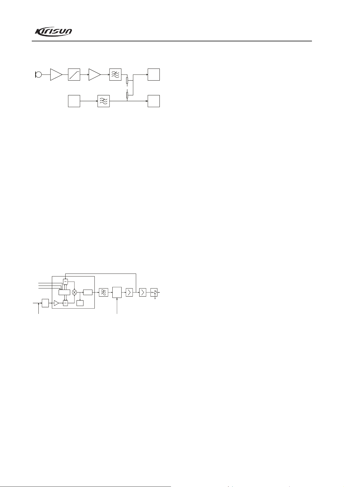
3.1 Frequency Configuration
Figure 3.1 Frequency Configuration
The reference frequency of the frequency synthesizer is
provided by crystal oscillator X4 (TCXO, 16.8MHz). The
receiver adopts double mixing. The first IF is 49.95MHz and
the second IF is 450kHz. The first local oscillator signal of
the receiver is generated by the frequency synthesizer. The
second local oscillator signal adopts the third harmonic
(50.4MHz) of the crystal oscillator X4 (TCXO, 16.8MHz).
Transmitter signal is directly produced by the frequency
synthesizer.
3.2 Principle of Receiver (RX)
Figure 3.2 Principle of Receiver
Front end
The signal coming from the antenna passes through the
RX/TX switch circuit (D1, D2, D4 and D5), and passes
through a BPF (C37, C227, L8, L15, C70, C126, D30, C218,
L9, C230, C128, D26, C217, L10, C229, C127 and D24) to
remove unwanted out-of-band signal, and is routed to the
low noise amplifier (LNA) consists of Q20 and its peripheral
components where it is amplified.
Output signal from the LNA passes through a BPF (L7,
C228, C47, D23, C219, L6, C182, C124, D22, C216, L5,
C132, C32 and D21) and goes to the first mixer (Q19).
PWM wave is output from pin 12 of the MCU. The wave
is filtered and rectified into adjustable voltage, which can
control the center frequency of the band pass filter through
changing capacity of the varactor diode (D21, D22, D23,
D24, D26 and D30).
First mixer
The receiving signal from LNA is mixed with the first
local oscillator signal from the frequency synthesizer to
produce the first IF signal (49.95MHz). Then the first IF
signal passes through crystal filter (XF1 and XF2) to remove
the adjacent channel signal and signal outside the adjacent
channel.
IF circuit
The first IF signal from the crystal filter is amplified by
the first IF amplifier (Q21), and is routed to the IF
processing IC (IC5, TA31136).
IF IC consists of the second mixer, second local
oscillator, IF amplifier, limiter, discriminator, and noise
amplifier.
The 16.8MHz frequency produced by TCXO (X4) is
multiple-amplified and then adopts the third harmonic
(50.4MHz) as the second local oscillator signal source. The
second local oscillator signal (50.4MHz) is mixed with the
first IF signal (49.95MHz) in IC5 to generate the second IF
(450kHz). And then the second IF signal is amplified and
limited in IC5, filtered in the ceramic filter (CF1, 450kHz),
and demodulated in IC5. After that, the demodulated signal
is routed to the audio circuit to output audio signal.
3
Page 5
PT4208 Service Manual
Figure 3.3 IF System
Audio signal processing
The voice signal processing circuit of the receiver
consists of IC6 and its peripheral circuits. After being
amplified in IC6-C, voice signal from IC5 is sent to IC4
(CTCSS signaling filtering circuit) and IC6-D respectively.
The signal is then amplified, deemphasized and filtered by
other units of IC6 to remove HF and LF components
contained in the audio frequency, with only voice
components within 300~3000Hz left. The resulting signal is
then routed to Q9 for amplifying. The amplified signal is
adjusted in volume potentiometer and then is routed to the
audio power amplifier (IC8).
operate, and the speaker sounds. Speaker impedance: 16.
Q38: RX audio signal switch
Q51: Warning tone switch
Q25: Alert tone switch
CTCSS signal filtering
Demodulated audio signal from IC5 may contain CTCSS
(Continuous Tone Control Squelch System) or DCS (Digital
Code Squelch) signal. The spectrum components of
CTCSS/DCS are within 67-250Hz. The filtering circuit
consists of IC4 can remove signals outside the CTCSS/DCS
spectrum, which enables the MCU to decode CTCSS/DCS
more accurately.
3.3 Principle of Transceiver (TX)
TX power amplification
Figure 3.5 Principle of Power Amplification and Antenna
Switch
The modulated RF signal from VCO is amplified in Q2,
Q3 and Q12, and is routed to Q11 for power amplification.
Grid bias of Q11 and Q12 is controlled by the APC
circuit. Through changing the grid bias voltage, the Tx
output power can be controlled conveniently.
APC (Automatic Power Control)
Figure 3.4 Audio Processing of Receiver
Squelch circuit
The demodulated signal from IC5 goes to the selective
noise amplifier consists of noise amplifier within IC5, C211,
R99, R100, C107 and R94 to remove the noise component.
The resulting signal is then amplified in Q7 and
demodulated in D17 and is routed to the MCU. MCU
identifies level of the noise and controls the squelch.
Audio power amplifier
The audio power amplifier circuit consists of IC8 and its
peripheral components.
The received audio signal, voice alert signal, alert tone
signal and warning tone signal are collected and pass
through the audio amplifier where it is amplified and output
to drive the speaker. The warning tone has no volume
limitation.
When AFCO is in high level, Q35 turns on, IC8 starts to
4
R167, R168 and R169 are used to test the power
amplification current. IC3A is the sampling amplifier for the
power amplification current. IC3B is the power comparator
amplifier.
If the Tx output power is too high, the power
amplification current and IC3A output will increase; IC3B
output voltage will decrease, so the bias voltage of Q11 and
Q12 will also decrease, which causes the Tx output power to
be lowered, and vice versa. Thus the output power of Tx can
keep stable under different working conditions.
MCU can set the power through changing the voltage
Figure 3.6 APC Circuit
Page 6
PT4208 Service Manual
input to IC3B.
Tx voice signal processing
MIC Amp
MIC
Pre-Emphasis
IC7A
CTCSS/DCS
MCU
Figure 3.7 Audio Circuit of Tx
The Tx voice signal processing circuit consists of IC7
and its peripheral components. After being amplified, limited
and filtered, the voice signal from MIC is routed to VCO for
modulation together with CTCSS/DCS signal.
The AGC circuit is consisting of D13, D308 and Q24.
When signal from MIC is too large, the AGC circuit will
lower the signal strength to make sure that no distortion
happens to the signal.
Q34 is the power switch of the voice processing circuit.
It is controlled by MCU. Power supply of IC7 will be turned
on when the radio is transmitting.
J2 is the jack for external MIC. When using external
MIC, the internal MIC will be turned off automatically. But
the internal PTT is still effective.
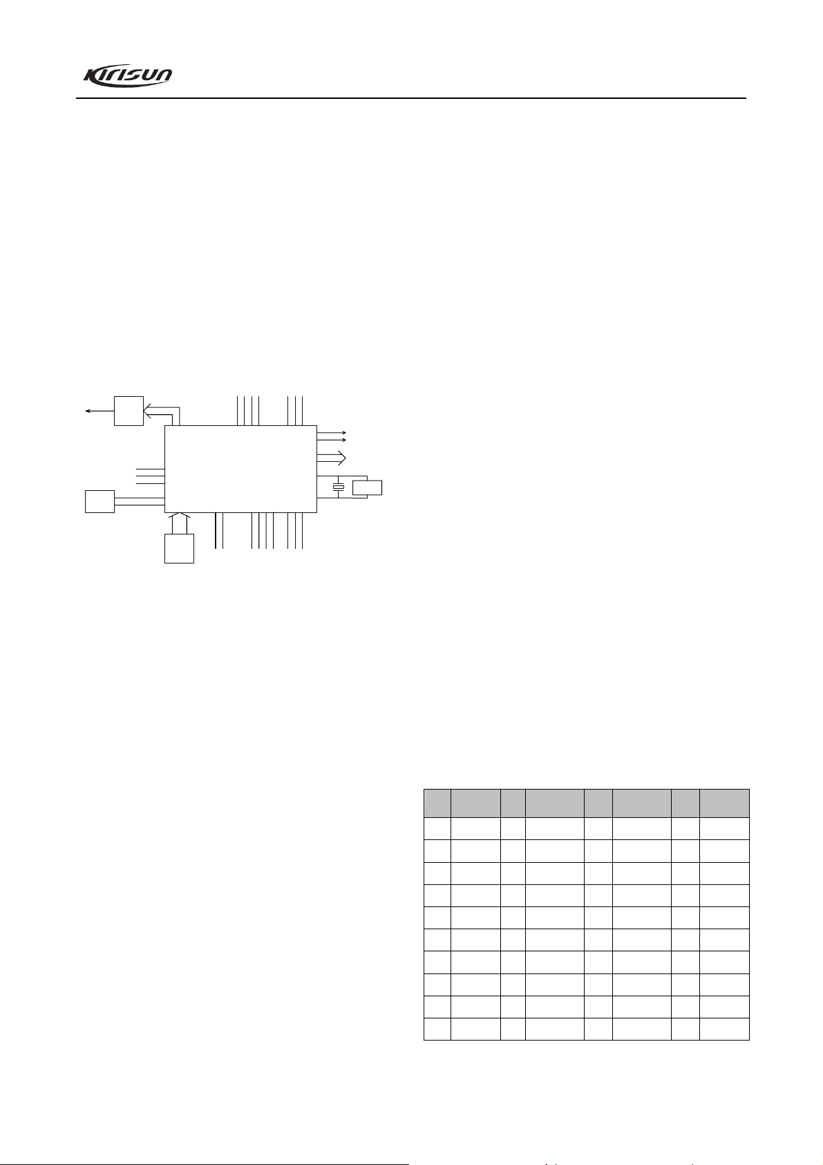
3.4 Principle of Frequency Synthesizer
to MCU
DCS Mod
Freq Adj
to MCU VCCN
TCXO
Data
CK
LE
1
N
Control Circuit
1
Nr
Detect
Charge
Pump
UL
Figure 3.8 Frequency Synthesizer
The radio adopts PLL type frequency synthesizer.
The frequency synthesizer consists of reference oscillator,
voltage control oscillator (VCO), programmable divider,
phase comparator, and low pass filter.
Rx VCO unit consists of Q14, L30, C120, C88, C142,
C180, D8 and D9. Tx VCO unit consists of Q15, L51, C121,
C137, C206, C194, D10 and D11. D12 is the modulation
circuit of VCO.
IC1 (MB15E03) is PLL integrated circuit, which consists
of programmable reference divider, programmable
swallowing divider, phase comparator, and charge pump.
The low pass filter consists of R244, C193, R202, R40,
C207, R141, C205, R2 and C204. The reference frequency is
IC7C,IC7D
IC7B
Q5
VCO
MOD in
VCO
TCXO
Q4
D3,D6
TX
RX
provided by X4 (TCXO, 16.8MHz).
The reference frequency from TCXO (Temperature
Controlled Crystal Oscillator) is divided by the
programmable reference divider in IC1 to produce reference
frequency of 5kHz or 6.25kHz (determined by the preset
channel frequency and is controlled by MCU).
The oscillation frequency from VCO goes to IC1 where
it is divided by the programmable swallowing divider and is
then compared with the reference frequency to obtain the
error signal. The signal is then filtered by a low pass filter
and is routed to VCO to change the oscillation frequency of
the VCO, enabling the frequency to reach the set value. Then
the VCO is locked.
N=F
VCO/FR
N: Times of frequency division
F
F
: Oscillation frequency of VCO
VCO
: Reference frequency
R
Unlock detection: When PLL is unlocked, Pin 14 of IC
will output the low level signal to MCU. Then MCU
prohibits the Tx from transmitting and makes an alert tone.
Q6: Power filter, which provides more purified power for
PLL to reduce noise of the frequency synthesizer.
3.5 Voice Alert Circuit
The radio is provided with voice alert function, which is
especially useful at night or in dark environment.
IC15 is a voice memory chip, which is stored with voices
of channel indication etc. Once the channel selector knob is
switched, the speaker will announce the current channel
number. User can press the preprogrammed “Voice Alert”
key to repeat the current channel number.
If voice alert function is enabled, the speaker will
announce the current channel number once the “Voice Alert”
key is pressed under standby mode. You can switch the voice
type by pressing and holding the “Voice Alert” key while
rebooting the radio. Do it repeatedly to switch the voice type
in the order of “Chinese Male-English Male-Chinese
Female-English Female-No Alert”.
3.6 Power Supply
The radio uses 7.4V, 1700mAh Li polymer battery. The
Tx power amplification circuit (Q11 and Q12) and the Rx
audio power amplifier (IC8) directly adopt the battery for
power supply. Power of other circuits is supplied by 5V
regulated voltage.
5
Page 7
PT4208 Service Manual
IC12: 5V, low dropout, micro-power regulator, which
supplies 5V power with large current for the radio together
with Q10 and Q30.
Q29: 5T switch, which is controlled by MCU.
5T: Supplies power for front end of Tx.
Q31: 5R switch, which is controlled by MCU.
5R: Supplies power for RF amplifier, mixer, IF
processing unit, and audio signal processing unit etc. of Rx.
Q32: 5C switch, which is controlled by MCU.
5C: 5V power supply under SAVE control. Supplies
power for frequency synthesizer.
3.7 MCU Unit
to PLL
APC CONTR
IC9
EEPROM
D/A
5TC
5RC
SAVE
chananl
SW
RXD
to PC
UL
LE
DATA
CK
IC10
MCU
TXD
PTT
MONI
VCCN
BEEP
CTCSS/DCS OUT
VIOCE CHIP
TX/RX CONTROL
SHIFT
PF1
ALARM
SQL
BATT
CTCSS/DCS IN
Figure 3.9 Principle of MCU Unit
MCU unit controls the operation of each unit of the radio
so that all functions can be realized.
Communicate with external PC.
Access the status data of the radio.
Control the PLL to generate Rx and Tx local oscillator
frequencies.
Obtain status parameters of current channel.
Control status of LED indicator.
Control power supply for each unit.
Check the actions of each functional key.
Generate CTCSS signal.
Generate DCS signal.
Generate power control signal.
Perform CTCSS decoding.
Perform DCS decoding.
Test and control the squelch.
Control content of voice alert.
Memory (E
2
PROM, A T24C08):
The memory is stored with channel data, CTCSS/DCS
data, other data for function setting, and parameter adjusting
data.
6
CTCSS/DCS signal encoding and decoding:
The CTCSS/DCS signal (output from pin 12) generated
by MCU is filtered by R155, R156, C242 and C243. Then
the resulting signal is divided into two parts and sent to VCO
and TCXO respectively for modulation.
The CTCSS/DCS signal from the receiver is decoded by
MCU (pin 49). MCU checks if the CTCSS/DCS signal in the
receiving signal matches the preset value of the radio, and
determines whether to open the speaker or not.
Power adjustment:
Output from pin 42 of the MCU passes through
integrating filter (R161, C317, R206, and C318), and is
routed to the APC unit to control the output power of the
transmitter.
CTCSS signal
CTCSS (Continuous Tone Control Squelch System) is a
squelch control system which is modulated on carrier and is
guided by a continuous sub-audio signal. If CTCSS is set,
the communication between the transmitting and receiving
radios can be realized only when the two radios has set the
same CTCSS frequency. In doing this, disturbance from
other signals can be avoided.
PT4208 has 39 groups of standard CTCSS frequencies
for your selection. See table 3.1.
The CTCSS signal is generated by MCU, and is passed
through low pass filter consists of RC to remove high
frequency components (above 300Hz). Then the resulting
signal is routed to VCO for modulation.
Table 3.1 CTCSS Frequencies
No. Frequency
1 67.0 11 94.8 21 131.8 31 186.2
2 69.3 12 97.4 22 136.5 32 192.8
3 71.9 13 100.0 23 141.3 33 203.5
4 74.4 14 103.5 24 146.2 34 210.7
5 77.0 15 107.2 25 151.4 35 218.1
6 79.7 16 110.9 26 156.7 36 225.7
7 82.5 17 114.8 27 162.2 37 233.6
8 85.4 18 118.8 28 167.9 38 241.8
9 88.5 19 123.0 29 173.8 39 250.3
10 91.5 20 127.3 30 179.9
[Hz]
No. Frequency
[Hz]
No. Frequency
[Hz]
DCS signal
No. Frequency
[Hz]
Page 8
PT4208 Service Manual
DCS (Digital Code Squelch), which is used to control
squelch, is a series of continuous digital codes modulated on
carrier together with voice signal. If DCS is set, the speaker
can be opened only when the radio receives signal with the
same DCS to avoid disturbance of unwanted signals.
PT4208 has 83 standard codes (inverted and
non-inverted) for your selection. See table 3.2.
DCS signal is produced by MCU (in waveform of PWM).
It passes through the low pass filter consists of RC to
remove the high frequency components (above 300Hz).
Then the resulting signal is sent to VCO and TCXO for
modulation, with HF components of the DCS signal being
modulated by VCO, and the LF components of the DCS
signal being modulated by TCXO.
The DCS signal coming from the receiver is routed to
MCU for decoding. MCU checks if the DCS code in the
received signal matches the preset DCS of the radio, and
determines whether to open the speaker or not.
Table 3.2 DCS Codes
023 114 174 315 445 631
025 115 205 331 464 632
026 116 223 343 465 654
031 125 226 346 466 662
032 131 243 351 503 664
043 132 244 364 506 703
047 134 245 365 516 712
051 143 251 371 532 723
054 152 261 411 546 731
065 155 263 412 565 732
071 156 265 413 606 734
072 162 271 423 612 743
073 165 306 431 624 754
074 172 311 432 627
3.8 Semiconductor Data
Refer to table 3.3 for descriptions of each pin.
Table 3.3 Definition of CPU Pins
No. Port name Pin Name I/O Function
1 TOPKEY P33 I Top key detect
2 UPKEY P34 I Up key detect
3 MODE I Connect the 4.7K resistor with VCC,
programming test point
4 PTT P43 I [PTT] input
5 DNKEY P44 I Down key detect
6 RST I Reset input, programming test point
7 XOUT O Oscillator
8 VSS I GND
9 XIN I Oscillator(7.3MHz)
7
10 VCC I 5V CPU power input
11 SHIFT P54 O Clock beat shift. H:On
12 TO0 P53 O (PWM) BPF tuning output
13 TO1 P52 O (PWM) QT/DQT output
14 VDEVC2 P51 I Deviation switch 2 of VHF
15 VDEVC1 P50 I Deviation switch 1 of VHF
16 NC Connect the pull-down resistor with VSS
17 PABC P26 O Final power supply H:On
18 OSCSI P25 I VCO crystal select and connect the
19 WNTC P24 O Wideband/Narrowband control.
20 ENC0 P23 I Encoder input
21 ENC2 P22 I Encoder input
22 ENC3 P21 I Encoder input
23 ENC1 P20 I Encoder input
24 PS P17 O PLL power-saving control. H: Normal L:
25 NC Connect the pull-down resistor with VSS
26 NC Connect the pull-down resistor with VSS
27 NC P86 Connect the pull-down resistor with VSS
28 SDA P85 I/O E2PROM data line
29 SCL P84 O E2PROM clock line
30 UL P83 I
I (TRFI)
31 T2IN P82 Reserved:2TONE input
32 DT P81 O PLL data output
33 CK P80 O PLL clock output
34 LE P60 O PLL IC enable pin. H: Locked
35 5MC P45 O Power control except CPU and E2PROM
36 INT P66 I Power detect input
37 TXD P67 O RS-232C output, programming test point
38 RXD P65 I RS-232C input, programming test point
39 AFCO P64 O AF amplification power
40 RX P63 O TX/RX VCO select H: Receiving
41 GLED P31 O Green LED control H: On
42 APC P30 O (PWM) TX: Automatic power control output
43 RLED P36 O Red LED control H: On
44 SAVE P32 O O Battery saving control. H:Supply power,
45 MUTE P13 O Mute control. H: MIC mute; L: Audio
46 5RC P12 Receiving power control. L: On
47 5TC O Transmitting power control. H:On
48 NC P10 Speaker mute switch output
49 TI P00 I (A/D8) QT/DQT signal input
50 RSSI I (A/D7) Signal strength detect
51 BUSY P01 I (A/D6) Busy signal input
52 MANDO
WN
53 BATT P03 I (A/D4) Battery voltage detect
54 NC Connect the pull-down resistor with VSS
55 W588C P62 O Voice alert switch. H: Channel No.
56 AC P61 O Alarm switch control. H: Controlled by
57 BUSY_V P05 I Voice alert circuit busy detect
58 VCCN P06 O (D/A0) Frequency stability output
59 AVSS I Connect with VSS
60 DTMF P07 O (D/A1) DTMF Output
61 VREF I Connect with VCC
62 AVCC I Connect with VCC
63 DATA_V P37 O Voice alert data
P02 I (A/D5) Man-down switch detect
pull-down resistor with VSS. H: 13, L:
16.8
H: Wideband L: Narrowband
Power Saving
PLL unlock detect pin
H: Locked L: Unlocked
L:On
H: On
L: Power saving
mute
reporting
Volume Switch
The power level must be low in case of
emergency alarm
Page 9
PT4208 Service Manual
64 SCLK_V P35 O Voice alert clock
Table 3.4 Function Description of Semiconductor
Components
Position
Mark
IC1 MB15E03 Frequency synthesizer
IC4 NJM2904 APC, voltage comparison, driving
IC5 TA31136 Rx second local oscillator, second IF
IC6 NJM2902 Amplification and filtering of demodulation
IC7 NJM2902 MIC amplification, limitation and filtering
IC8 TDA8541 Audio frequency power amplification of
IC9 AT24C08 E2PROM, memorizes channel frequency data,
IC10 R5F212A8 MCU
IC11 PST9140NR MCU reset circuit
IC12 HT7150-1 LDO, low-power voltage regulator
IC15 W588A080 Voice storage IC
Q2 2SC5108 First amplification of transmitter
Q3 2SC3356 Second amplification of transmitter
Q4 2SC5108 VCO buffer amplifier
Q5 2SC5108 VCO buffer amplifier
Q6 2SC4617 VCO power filter
Q7 2SC4738 Noise amplifier
Q9 2SC4617 Audio frequency signal amplification of
Q10 2SC1623 5V voltage regulation output current stretching
Q11 RD07MVS1 Transmitter final power amplification
Q12 RD01MUS1 Transmitter power amplification driving
Q17 DTA144EE APC output switch
Q19 3SK318 First mixer
Q20 3SK318 Receiver high power amplifier
Q21 KTC4082 1st IF Amplifier
Q22 DTC144EE Red LED Driving
Q23 DTC144EE Green LED Driving
Q24 2SK1824 Voice alert switch
Q26 DTC144EE 5C switch
Q29 KTA1298 5T switch
Q30 KTA1298 5V voltage regulation output current stretching
Q31 KTA1298 5R switch
Q32 KTA1298 5C switch
Q34 DTA144EE Power switch of MIC amplification unit
Q35 2SK1824 Receiver audio output switch. Disconnect on
Q36 2SK1824 Receiver audio output switch
Model Function Description
amplification, limitation, demodulation, and
noise amplification
signal of receiver.
receiver
function setting parameters and adjusting
status parameters
receiver
Emergency
Table 3.5 Function Description of Diodes
Position
Mark
D1 MA77 Transmitter antenna switch diode
D2 MA77 Transmitter antenna switch diode
D3 HSC277 VCO output switch
8
Model Function Description
D4 HSC277 Antenna toggle switch
D5 HSC277 Antenna toggle switch
D6 HSC277 VCO output switch
D7 HSC277 5V voltage regulation output current stretching
D8 HVC376B VCO oscillation varactor diode
D9 HVC376B VCO oscillation varactor diode
D12 MA360 VCO modulation diode
D14 HZU5ALL APC output voltage-limiting diode
D15 MA2S111 Unlock detection diode
D16 MA2S111 VCO power filtering acceleration diode
D17 1N4148 Noise demodulation
D18 1N4148 Noise demodulation
D20 Green
Receiving indicator
LED
D25 MA2S111 APC single diode
D28 Red LED Transmitting indicator
D29 Green
Receiving indicator
LED
Table 3.6 Features of Crystal Filter XF1, XF2
Item Rated Value
Nominal center frequency 49.95MHz
Passband width ±7.5kHz or higher
40dB stop bandwidth ±20.0kHz or lower
Pulse 1.0dB or lower
Insertion loss 3.0dB or lower
Guarantee attenuation 80dB or higher
Terminal impedance ---
Table 3.7 Features of CF1 LTVPC450EB
Item Rated Value
Nominal center frequency 450kHz
6dB bandwidth ±6kHz or higher
50dB bandwidth ±12.5kHz or lower
Pulse 2.0dB or lower
Insertion loss 6.0dB or lower
Guarantee attenuation 35.0db or higher
Terminal impedance 2.0k
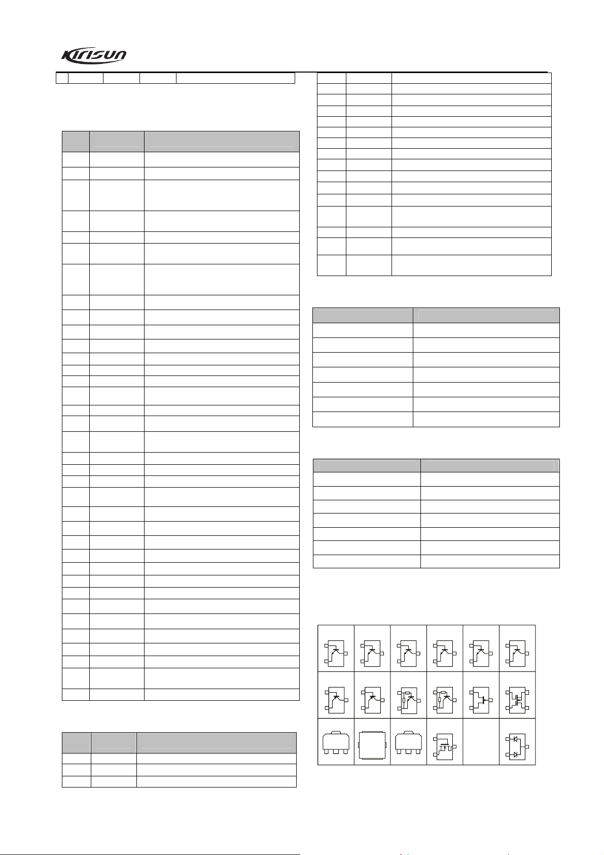
Table 3.8 Schematic Diagram for Packaging of
Semiconductor Devices
B
E
B
E
RD01MUS1
GSD
2SC5108
M: MC
KTA1298
2SC3356
M: R24
B
C
E
FMMT591
B
E
RD07MVS1
D
RDA0002
S
G
C
C
S
2SC4617
B
E
DTC144EE
M:16
B
E
HT7150-1
GNDINOUT
2SC4738
B
C
E
DTA144EE
B
C
E
2SK1824
Mark: B1
G
S
KTC4082
B
C
E
2SK308NV
S
CC
D
D
2SC1623
M: L6
B
C
E
3SK318
M: YB-
G1
G
G2
DA221
M: K
1
2
C
S
D
3
Page 10
PT4208 Service Manual
Chapter 4 Mode Introduction
Mode Introduction
Mode Function How to enter
User Mode For normal use Power ON
Data
Programming
Mode
PC
PC Test Mode
Mode
Firmware
Programming
Mode
Wired Clone Mode
* User Mode
You can enter User Mode (conventional communication
mode) by turning the radio power ON. Under this mode,
users can use the defined functions of the radio.
* Data Programming Mode
The radio has been set before leaving the factory.
However, due to different requirements of users, the radio’s
operating frequency, channels, CTCSS/DCS, scan, and other
functional parameters should be reprogrammed. Therefore,
Kirisun has specially designed a set of Chinese/English
programming software KSP4208 with friendly interface,
convenient operation and visualized display for setting
functional parameters of the radio.
Steps for setting the functional parameters of the radio by
PC are as follows:
A. Install KSP4208 on the computer.
B. Connect the radio to the serial port of the PC with
the special programming cable. Refer to the figure
below.
Computer
(RS232 serial port)
Figure 4.1
C. Turn the computer power ON.
D. Turn the radio power ON.
E. Run the KSP4208 programming software by
double clicking on its executive program.
F. Click “Program” in the main menu of KSP4208,
Used to read and write
frequency data and
other features to and
from the radio
Tune the radio
parameters by PC
Upgrade the radio
when new features are
released
Used to transfer
programming data
from one radio to
another
Programming
cable
Received commands
from PC. See below for
further information.
Received commands
from PC. See below for
further information.
Press and hold the top
key for over 2 seconds
while turning the radio
power ON, and received
commands from PC
Press and hold side key 2
for over 2 seconds while
turning the radio power
ON
(Earphone/Program
Radio
ming interface)
and click “Read from radio” in the pull-down menu
to read parameters of the radio to the computer;
click “Write to radio” in the pull-down menu to
write parameters in the computer to the radio.
G. The following parameters can be set by using
KSP4208 according to requirements of the user:
Radio Information:
Radio Model (model/frequency range), Serial Number,
Embedded Information, MCU Version, Hardware Version,
etc.
Radio Configuration:
(1) Key Assignment: Side Key 1 (Up Key), Side Key 2
(Down Key), and Top Key can be set as long/short key and
the hold time can be defined.
(2) Miscellaneous
1. Wired Clone Mode
2. TOT (Time Out Timer)
3. TOT Reset
4. TOT Pre-alert
5. TOT Re-key time
6. Squelch Level selection
7. Alert Tone
8. Read Data Password
9. Write Data Password
(3) Scan
Scan Function option, Priority Channel, Revert Channel,
Tx Dwell Time, Dropout Delay Time, Lookback Time.
(4) Emergency settings
Channel Parameters
(1) Rx Frequency and Tx Frequency (Step:
2.5KHz/5KHz/6.25KHz)
(2) Rx Signaling and Tx Signaling
a) None
b) CTCSS (60~260Hz @ 0.1Hz step)
c) DCS (-777~777@octal number)
(3) Busy Channel Lockout (BCL)
(4) Beat Shift
(5) Channel Spacing: 25KHz/12.5KHz (Wide/Narrow)
(6) Scan Add/Delete
(7) Tx Power (High/Low)
(8) Clear Tail Tone
(9) CALL1 and CALL2 encode
(10) PTT ID Keyup Telegram, PTT ID Dekey Telegram
DTMF Setting
DTMF Encoder Template
9
Page 11

PT4208 Service Manual
DTMF Encoder Sequences (1~12)
Please refer to the “Help” document of KSP4208 for
details.
Note:
1. Please firstly read data of the radio and back up the data
before editing the parameters on KSP4208.
2. If the radio cannot function normally after being written in
with the edited data, please rewrite the backup data into the
radio.
3. “Model Information” is important for the radio; users
should not modify it.
* PC Test Mode
Connect the radio to the serial port of the computer with
the special programming cable. Refer to figure 4.1.
Warning: Before entering the PC Test Mode, please firstly
connect a 50 HF load to the antenna connector of the radio
or connect the radio to a general test set.
With the KSP4208 programming software, you can enter
the Tuning Mode under PC Test Mode to tune the following
parameters of the radio:
(1) Frequency stability
(2) Five frequency points of Tx High Power
(3) Five frequency points of Tx Low Power
(4) Five frequency points for SQL9 On (Wideband)
(5) Five frequency points for SQL9 Off (Wideband)
(6) Five frequency points for SQL9 On (Narrowband)
(7) Five frequency points for SQL9 Off (Narrowband)
(8) Five frequency points for SQL1 On (Wideband)
(9) Five frequency points for SQL1 Off (Wideband)
(10) Five frequency points for SQL1 On (Narrowband)
(11) Five frequency points for SQL1 Off (Narrowband)
(12) Five frequency points for QT (67.0Hz) Deviation
(Wideband)
(13) Center frequency point for QT (67.0Hz) Deviation
(Narrowband)
(14) Five frequency points for QT (151.4Hz) Deviation
(Wideband)
(15) Center frequency point for QT (151.4Hz) Deviation
(Narrowband)
(16) Five frequency points for QT (254.1Hz) Deviation
(Wideband)
(17) Center frequency point for QT (254.1Hz) Deviation
(Narrowband)
(18) Five frequency points for DQT Deviation (Wideband)
(19) Center frequency point for DQT Deviation
(Narrowband)
(20) Five frequency points for Rx Sensitivity
(21) Center frequency of DTMF Deviation (Wideband and
Narrowband)
(22) Tx Low Voltage
(23)
Rx Low Voltage
* Firmware Programming Mode
The radio is in possession with an internal Flash ROM
which can be upgraded when new features are released.
Procedure:
1. Press and hold the Top Key for over 2 seconds while
turning the radio power ON. The LED will light orange
and the radio enters the Firmware Programming Mode.
2. Run the firmware programming software KMU on PC.
3. Connect the radio to the computer by the programming
cable.
4. Select a COM port and load the firmware upgrading file.
Then click on “E.P” to start downloading.
5. If the communication ends successfully, turn the radio
power OFF to exit.
6. If you want to continue programming other radios,
repeat steps 1 to 5.
* Wired Clone Mode
If the wired clone function is enabled, the radio can enter
the Wired Clone Mode. After entering this mode, the radio
will not exit automatically. The user needs to reboot the
radio if he wants the radio to return to the User Mode.
The operation is as follows:
1. Press and hold Side Key 2 for over 2 seconds while
turning the radio power ON to enter the Wired Clone
Mode. The radio will enter User Mode if wired clone
function is disabled.
2. Connect the slave radio to the master radio by the
cloning cable (KCL-01) and turn on the power of the
slave radio.
3. Press Side Key 1 on the master radio to start cloning.
Then the red LED on the master will light. The data of
the master is sent to the slave. While the slave is
receiving the data, the LED lights green. When cloning
of data is completed, the red LED on the master will go
out, and the slave radio will reboot automatically.
10
Page 12
PT4208 Service Manual
4. The other slaves can be continuously cloned. Carry out
the operation in step 3.
Note: The user can enable or disable the wired clone
function through PC programming software. Once the wired
clone function is disabled, the radio cannot enter the Wired
Clone Mode.
Chapter 5 Assembly and Disassembly for
Maintenance
The radio is a kind of sophisticated communication
equipment with precise structure and small size. You should
assemble and disassemble it carefully during the
maintenance. The instructions for the assembly and
disassembly are as follows.
5.1 Install/Remove the battery
1) Install the battery
Insert the two protrusions at the lower end of the battery
into the holes at the lower end of the shell of the radio.
Note:
* Never short the terminals of the battery.
* Do not throw the battery into fire.
* Do not remove the housing of the battery by yourself.
5.2 Install/Remove the belt clip
Slide the guide rails on the belt clip along the guide slots
on the rear of the battery with proper strength until the belt
clip is hooked. When removing the belt clip, lift the sheet
metal on the top of the belt clip with your finger nail or a
tool while pushing the belt clip upward.
Press down the upper part of the battery until the latch on
the radio completely bounces out and locked.
2) Remove the battery
Press the back of the battery slightly, and push the latch
upward. Then remove the battery from the radio.
11
5.3 Remove the front cabinet from the chassis
1) Pull out the knobs and screw off the antenna;
2) Remove the two nuts of the knobs and one nut of the
antenna with a special tool;
3) Screw off the screw on the earphone jack cover with a
cross screwdriver, and then remove the rubber cover;
4) Remove the two rubber plugs on the screws of the coping;
screw off the screws by a hexagonal screwdriver, and then
take off the coping;
5) Remove the two fixing screws at the lower part of the Al
chassis by a hexagonal screwdriver;
6) Insert a flat-blade screwdriver into the slot at the bottom
of the Al chassis, and prize up it. Then pull the Al chassis
backward to remove it from the front cabinet. Please be
careful not to break the cable of the speaker.
Refer to Figure 5.5.
Page 13
PT4208 Service Manual
Figure 5.5
5.4 Remove the main board from the Al chassis
1) Remove the screws from the PCB board by a cross
screwdriver;
2) Remove the solder of the antenna terminal with a
soldering iron. Then take off the main board.
Refer to Figure 5.6
Figure 5.6
After the aforesaid disassembly, you can repair and
adjust the radio according to its actual malfunction.
1
2
3
4
5
6
7
8
9
10
Figure 5.7 Exploded View
No. Part No. Description PCS
1 710-420470-R06 Antenna 1
2 201-004208-R07 Channel Selector Knob 1
3 201-004208-R06 Volume Knob 1
4 203-003208-R09 Circlip 2
11 12 13
17 18 19 20 21 22
36
35
26 32 33 34
25
23 24
27
37
28 29 30 31
14
15
16
5 203-007200-R07 Nut for Antenna Socket 1
6 203-000558-R02 Nut for Knob 2
7 201-004208-R09 Light Guide 1
8 201-004208-R01 Front Cabinet 1
9 201-004208-R08 Earphone Jack Cover 1
10 301-25080J-R01 Screw M2.5*8.0 1
11 202-004208-R01 Main Waterproof 1
12 201-004208-R02 Coping 1
13 301-25050J-R01 Screw M2.5*5.0 2
14 202-007200-R07 Rubber Plug 2
15 203-000558-R05 Spring for Battery Latch 1
16 201-004208-R03 Battery Latch 1
17 204-003208-R02 Dust-proof Net for Speaker 1
18 202-004208-R02 Rubber PTT Key 1
19 201-004208-R04 PTT Key 1
20 121-100000-R20 Speaker 1
21 301-20040G-R01 Screw M2.0*4.0 12
22 602-04208X-HXX Main Board 1
23 201-004208-R05 POGO Pin Socket 1
24 203-004208-R02 Earphone Plate 1
25 203-000558-R07 Antenna Socket 1
26 204-004208-R02 Dust-proof Net for MIC 1
27 202-007200-R06 POGO Pin Waterproof 1
28 203-004208-R01 Al Chassis 1
29 301-20080G-R02 Screw M2.0*8.0 2
30 204-007200-R03 Sponge for POGO Pin 1
31 706-0KB70B-R01 Battery 1
32 202-004208-R03 MIC Rubber Waterproof 1
33 120-100000-007 Plastic-packaged Wire 1
34 120-100000-008 Plastic-packaged Wire 1
202-003208-R07 Heat Exchange Silicone
35
Rubber Washer
1
36 204-006500-R02 MIC Socket Guardian 1
37 204-0KB36L-R03 Sponge Cushion 1
Chapter 6 Adjustment
Before test/adjustment, make sure all equipment has
been well connected to the ground!
Before test/adjustment, make sure the antenna output
terminal has been correctly connected to corresponding
equipment or load!
The transmitter output terminal must be terminated with
12
Page 14
PT4208 Service Manual
an RF power attenuator and connected to a standard signal
generator (SSG)/frequency counter/deviation
meter/spectrum analyzer!
Make sure no transmission operation is being conducted
while measuring the receiver!
During the adjustment/test/maintenance, make sure
reliable anti-static measures are taken for human body and
equipment.
6.1 Equipment and Software Required for Test and
Adjustment
Equipment and software listed in Table 6.1 are required
for test and adjustment of PT4208.
Table 6.1 Equipment and Software Required for Test and
Adjustment
No. Name Major Specifications
1 Computer
Programming
2
software
Programming
3
cable
4 Clone cable KCL01
DC regulated
5
power supply
6 RF power meter
Frequency
7
counter
8 Deviation meter
9 DMM
Audio signal
10
generator
RF power
11
attenuator
Standard signal
12
generator
13 Oscilloscope
Audio frequency
14
voltmeter
Recommendation: Item 6, 7, 8, 10, 11, and 12 listed in
the table can be replaced by HP8920 general test set.
P2 or above, IBM compatible PC, WINDOWS
98/ME/2000/XP Operating System
KSP4208
Output voltage:7.5V
Output current: 5A
Measurement range: 0.5-10W
Frequency range: 100MHz-500MHz
Impedance: 50
SWR1.2
Frequency range: 0-1600MHz
Frequency accuracy: better than ±1×10⁻⁶
Sensitivity: better than 100mV
Frequency range: DC600MHz
Measurement range: 0-±5kHz
Input impedance: above 10M/V DC, capable of
measuring voltage, current and resistance.
Frequency range:2-3000Hz
Output level: 1-500mV
Attenuation: 40dB or 50dB
Supporting power : higher than10W
Frequency range:10MHz-1000MHz
Output level: 0.1uV-32mV (-127dBm~-17dBm)
Frequency range: DC~20MHz
Test range: 10mV-20V
Test range: 10mV-10V
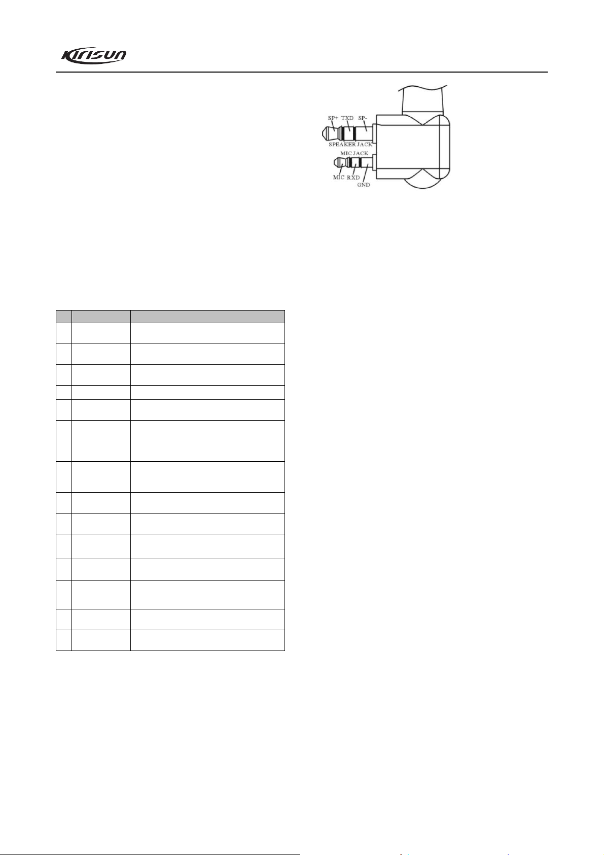
Figure 6.1 External Speaker/MIC Plug
6.2 Adjustment Items
After changing components during the maintenance, it is
necessary to test the radio and adjust its technical parameters.
The following part is going to introduce the adjustment
items.
Some parameters can be adjusted by use of KSP4208
programming software (in the Tuning Mode). The adjustable
parameters are as follows:
1) 6250Hz stability/2500Hz stability
2) Tx high power/low power
3) BATT Tx low voltage /Rx low voltage
4) SQL9/SQL1 On/Off
5)
QT DEV
6) DCS DEV
7) DTMF DEV
8) Rx sensitivity
Steps for adjustment:
a. Enter PC Test Mode. Refer to Chapter 4.
b. Click “Edit” in the main menu of KSP4208
programming software, and then click “Entry Tuning” in the
pull-down menu to enter the Tuning Mode.
c. Then the “Tuning Item List” screen will pop up.
Double click the item you want to adjust, and then you can
adjust the parameters.
d. Exit the PC Test Mode after adjustment.
6.3 Adjustment
6.3.1 VCO
Disable the “Battery Save” function, and set the Rx
frequency to the low frequency point (see Table 6.2). Under
the receiving status, measure the voltage of PD by DMM.
Then adjust the PD voltage to be 0.7V±0.3V by tuning the
trimming capacitor C180.
Set the Tx frequency to the high frequency point (see
13
Page 15

PT4208 Service Manual
Table 6.2), and press the PTT key. Then measure the voltage
of PD by DMM. The resulting voltage should be lower than
4.5V.
Table 6.2 High/Center/Low Frequency Point for PT4208
Low Freq Point Center Freq Point High Freq Point
PT4208(1) 136.125 MHz 145.125 MHz 173.975 MHz
PT4208(2) 400.125MHz 425.125MHz 449.975MHz
PT4208(3) 420.125MHz 445.125MHz 469.975MHz
6.3.2 PLL frequency
In the Tuning Mode, double click the “6250Hz
stability/2500Hz stability” item to enter. Adjust the
parameter within the adjusting range of 0-255 to make the
Tx frequency be the rated value (with error within ±200Hz).
6.3.3 Tx power
In the Tuning Mode, double click the Tx “High power”
item to enter. Adjust the five frequency points of “Lowest”,
“Low”, “Mid”, “High” and “Highest” within the adjusting
range of 0-255 to make the Tx power be higher than 4W.
Meanwhile, observe the operating current, and make sure
that the current is no larger than 1.7A.
In the Tuning Mode, double click the Tx “Low power”
item to enter. Adjust the five frequency points of “Lowest”,
“Low”, “Mid”, “High” and “Highest” within the adjusting
range of 0-255 to make the Tx power be higher than 1W.
See Table 6.5 for detailed parameters.
6.3.4 Tx low voltage/Rx low voltage for BATT
Firstly, adjust the power voltage to be 6.8V. Double click
the “Tx low voltage/Rx low voltage” in the Tuning Mode.
Click “Begin” to let the software test automatically. When
the value changes no more or only changes a little, click
SAVE to exit.
6.3.5 Max. deviation
Input audio signal (100mV, 1000Hz) to the MIC jack of
the radio. Adjust the potentiometer VR2 to make the Max.
deviation be ±4.5kHz.
6.3.6 DCS Tx signal waveform and deviation
In the Tuning Mode, double click the “DCS DEV” item
to enter. Adjust the potentiometer VR1 and observe the
demodulation signal (the waveform should be smooth and
similar to square wave). Click wideband, and adjust the five
frequency points of “Lowest”, “Low”, “Mid”, “High”, and
“Highest” to make the deviation be 0.8kHz. Then click
narrowband, and adjust the five frequency points to make the
deviation be 0.4kHz.
6.3.7 CTCSS deviation
In the Tuning Mode, double click the “QT(67.0) DEV”
item to enter. Click wideband, and adjust the five frequency
points of “Lowest”, “Low”, “Mid”, “High”, and “Highest” to
make the deviation be 0.75kHz. Then click narrowband, and
adjust the value to make the deviation be 0.35kHz.
In the Tuning Mode, double click the “QT(151.4) DEV”
item to enter. The tuning method is the same as that of
“QT(67.0) DEV”.
In the Tuning Mode, double click the “QT(254.1) DEV”
item to enter. The tuning method is the same as that of
“QT(67.0) DEV”.
6.3.8 Rx sensitivity
In the Tuning Mode, double click the “Sensitivity” item
to enter. Adjust the five frequency points of “Lowest”,
“Low”, “Mid”, “High”, and “Highest” within the adjusting
range of 0-255 to make the sensitivity be the highest.
See Table 6.4 for detailed parameters.
6.3.9 Rx squelch
In the Tuning Mode, double click the “SQL9 On” item to
enter. Click wideband and use the following method to
adjust the five frequency points of “Lowest”, “Low”, “Mid”,
“High”, and “Highest” respectively. Firstly, click one of the
frequency points, and adjust the RF signal frequency of the
test equipment to be the same with the receiving frequency
of that frequency point, and adjust the signal level to be
-116dBm. Then adjust the frequency of the modulation
signal to be 1kHz and the deviation to be 3kHz. Click
“Begin”, the programming software will adjust the value
automatically. When the value keeps stable, click “OK”, the
adjustment of that frequency point is completed. Then click
the next frequency point to do the adjustment. After all of the
five frequency points are adjusted, use the same method to
adjust the five frequency points of the narrowband. The only
difference is that the frequency of the modulation signal
should be 1kHz, and the deviation should be 1.5kHz.
In the Tuning Mode, double click the “SQL9 Off” item
to enter. Click wideband and use the following method to
adjust the five frequency points of “Lowest”, “Low”, “Mid”,
14
Page 16
PT4208 Service Manual
“High”, and “Highest” respectively. Firstly, click one of the
frequency points, and adjust the RF signal frequency of the
test equipment to be the same with the receiving frequency
of that frequency point, and adjust the signal level to be
-118dBm. Then adjust the frequency of the modulation
signal to be 1kHz and the deviation to be 3kHz. Click
“Begin”, the programming software will adjust the value
automatically. When the value keeps stable, click “OK”, the
adjustment of that frequency point is completed. Then click
the next frequency point to do the adjustment. After all of the
five frequency points are adjusted, use the same method to
Table 6.3 VCO
Item Test Condition
Setting
VCO lock
voltage
Item Test Condition
Audio level
Sensitivity
SQL On
sensitivity
Item Test condition Test equipment
Tx
frequency
DCS
waveform
(balance)
BATT terminal
voltage: 7.5V
CH: Rx low freq
point
CH: Tx high freq
point
Test freq: Mid freq
point
Antenna input:
RF OUT: -53dBm
(501V)
MOD: 1kHz
DEV: ±3.0kHz
Audio load: 16
CH: Mid freq point
CH: Low freq point
CH: High freq point
RF OUT: -119dBm
(0.25V)
MOD: 1kHz
DEV: ±3.0kHz
CH: Rx center freq
point
Level 9
RF OUT: -116dBm
Level 1
RF OUT: -123dBm
Tes t
Equipment
DMM PD
Equipment
RF signal
generator
Oscilloscope
frequency
voltmeter
Distortion
/General test
Measurement
Ter min al
Table 6.4 Receiver Section
Tes t
Audio
meter
set
Frequency counter
/ General test set
Oscilloscope /
General test set
Measure
ment
Ter min al
Speaker
connector
Table 6.5 Transmitter Section
adjust the five frequency points of the narrowband. The only
difference is that the frequency of the modulation signal
should be 1kHz, and the deviation should be 1.5kHz.
In the Tuning Mode, double click the “SQL1 On” and
“SQL1 Off” item to enter respectively. Use the same method
stated above to do the adjustment. The only difference is that
the RF signal level for “SQL1 On” should be 123dBm, and
the RF signal level for “SQL1 Off” should be 125dBm.
6.4 Adjustment Description
See Table 6.3, 6.4, and 6.5.
Adjustment
Parts
C180 0.7V±0.3V Adjustment
Adjustment
Parts
PC Tuning
Mode
PC Tuning
Mode
Measuring
terminal
Antenna
Requirement Remark
Lower than
4.5V
Requirement Remark
(Turn the
volume knob
clockwise to
the end) Audio
power >
0.3W
SINAD: 12dB
or higher
Normal
squelch on
after
adjustment
Normal
squelch on
after
adjustment
Adjustment
parts
PC Tuning
Mode
VR1
Requirement Remark
Within ±200Hz
similar to square
Observation
Internal speaker
power > 1.2W
Smooth and
wave
15
Page 17

PT4208 Service Manual
Power Power: 7.5V
Max
modulation
deviation
Modulation
sensitivity
CTCSS
DEV
CH:Tx center freq point
AG:1kHz/220mV
CH:Tx center freq point
AG:1kHz/22mV
CTCSS:67Hz
DCS DEV DCS:023N
Low
battery
Battery terminal: 6.8V
Chapter 7 Specifications
Technical Parameters
7.1 General Specifications
Frequency
Number of Channels 16
Channel Spacing W:25 kHz /N:12.5kHz
Operating Temperature -25℃~ +55℃
Antenna Impedance 50
Frequency Stability ±2.5ppm
Battery (Standard
Configuration)
Dimension (W×H×D) 54mm × 119mm × 34mm
Weight 157g (Radio only);
7.2 Receiver
Sensitivity (12dB
SINAD)
Adjacent Channel
Selectivity
Intermodulation
Interference
Audio Output Power 1W (16)
Audio Distortion 5%
7.3 Transmitter
Transmitting Power 4W(UHF) / 5W(VHF)
Modulation Mode W:16KF3E / N:11KF3E
Clutter and Harmonic -36 dBm
Residual FM
(300~3000Hz)
PT4208
(136 ~ 174) MHz (400 ~ 450) MHz
(350 ~ 390) MHz (420 ~ 470) MHz
Lithium Polymer Battery: 1700mAH 7.4V
255g: with antenna and 1700mAh Lithium
Polymer Battery
330g: with antenna and 1350mAh Ni-MH
Battery
0.25V(W) / 0.28V(N)
W: 70dB / N: 60dB
65dB
W:-45 dB / N:-40dB
Power meter/
General test set
Ammeter
Deviation meter/
General test set
Deviation meter/
General test set
Deviation meter/
General test set
PC Tuning
Mode
VR2
Adjust to 4W
Adjust to
±4.5kHz
Within
±0.2W
±200Hz
Deviation
checked should
be
2.2kHz~3.6kHz
PC Tuning
Mode
PC Tuning
Mode
PC Tuning
Mode
Audio Distortion
(300~3000Hz)
Adjacent Channel
Power
Max. Deviation W:<±5kHz / N:<±2.5kHz
Adjust to
±0.75kHz
Adjust to
±0.75kHz
Indicator flashes
after adjustment
5%
W: 70dB / N: 60dB
±50Hz
±50Hz
Chapter 8 Troubleshooting
No. Problem Causes and Solutions
1 Power on
Failure
2 PLL
unlocked
(Beeping)
3 No talkback A. The frequency of the radio’s current channel is not
4 No receiving
signal
A. Unreliable connection between the battery and the
radio, please reinstall the battery.
B. The fuse of the power supply is burnt out. Please
change it.
C. Power switch in failure, please change it.
D. The battery is out of power. Please charge it or
change a new one.
E. The CPU is broken, please change the IC.
A. Channel frequency goes beyond the limit, please
reset the channel data.
B. The PLL crystal oscillator X4 is broken. Please change
it.
C. The oscillator transistor is broken. Please change
it.
D. The PLL IC1 is broken. Please change it.
the same with that of the other radio. Please
reselect a channel.
B. The CTCSS/DCS is not the same. Please reset it.
C. The radio is out of the effective communication
range.
A. The antenna is in poor contact. Please fasten the
antenna until secure.
B. The high-frequency amplifying tube Q20 is
broken. Please change it.
C. The squelch level is too high and the squelch cannot be
opened. Please reset the squelch level.
D. The mixing tube Q19 is broken. Please change it.
16
Page 18

PT4208 Service Manual
E. The FM processing chip IC5 is broken. Please
change it.
5 The
transmitting red
light is on, but
no voice is
heard by the
recipient.
6 The receiving
green light is
on, but no voice
is heard.
A. Power module Q11 is broken, so there is no power
output, please change the module.
B. The microphone is broken, please change it.
A. The speaker is broken. Please change it.
B. The audio power amplifier IC8 is broken. Please
change it.
Chapter 9 KBC-70C Charger
9.1 General
Function: Intelligent rapid charging
Applicable battery: KB-70B (1700mAH, 7.4V Li-ion battery)
/ KB-70A (1350mAH, 7.2V Ni-MH Battery)
Identification for battery type: External
Input power: DC12V, 500mA, ripple < 500mV
9.2 Operating Environment
Temperature: -5℃ ± 2℃ ~ +55℃ ± 2℃
Humidity: 95%@40℃
9.3 Safety Requirement
Comply with CCC, CE, UL and other safety
requirements.
9.4 Specifications
* Idling input current: 15mA
* Charging terminal maximum idling voltage: 96% ~ 97% of
the input voltage
* Rapid charging current: 410 ± 25mA
* Max. charging time of Ni-MH battery: 285 minutes ± 15
minutes
* Max. charging time of Li-ion battery: 510 minutes ± 30
minutes
* Max. charging voltage: 9.6V ± 0.2V
* Highest battery temperature: +50℃ ± 2℃
* Specified voltage for charged battery:
Ni-MH battery: Pre-charge when the voltage is lower than
5.5 ± 0.1V. When the battery voltage reaches 6.5 ± 0.1V, the
17
charging turns to rapid charging. Or pre-charge when the
voltage is lower than 8.3V ± 0.1V. When the battery voltage
reaches 9.6V ± 0.2V, the battery will be deemed as full and
the charging will stop.
Li-ion battery: Pre-charge when the voltage is lower than
6.5 ± 0.1V. When the voltage reaches 6.5 ± 0.1V, the
charging turns to rapid charging.
* During the charging process, battery voltage, battery
temperature rise, - V△ , charging time, max. battery
temperature will be checked.
* Min. battery voltage:
Ni-MH battery: 5.5V ± 0.1V
Li-ion battery: 6.5V ± 0.1V
* Pre-charge current for battery:
Ni-MH battery: 180mA ± 10mA
Li-ion battery: 90mA ± 10mA
* Pre-charge time: 15 ~ 20 minutes
* Check the battery voltage during the pre-charging process,
when the voltage reaches the threshold of the battery, the
charging will turn to rapid charging.
* Conditions for stopping charging:
Normal conditions: The battery is fully charged. Ni-MH
battery: - V△ = 30mV ~ 60mV
Abnormal conditions:
(1) The battery temperature is higher than the limit.
(2) The battery voltage is higher than the limit.
(3) The charging time exceeds the limit.
(4) In the pre-charging process, the battery voltage fails to
reach the min. voltage allowed for normal battery.
* Status of the charger after the charging is finished: Ni-MH
battery enters trickle charging status (current: 30mA ±
10mA).
* Charging efficiency:
After being charged under normal temperature, the
battery capacity should not be lower than 90% of its actual
capacity.
After being charged under high temperature, the battery
capacity should not be lower than 70% of its actual capacity.
After being charged under low temperature, the battery
capacity should not be lower than 80% of its actual capacity.
* Other functions:
1. Charging indication
2. Abnormal charging indication
3. Pre-charging function for over-discharged battery
4. Trickle charging function for Ni-MH battery
Page 19

PT4208 Service Manual
5. Output short circuit protection function (the current for
short circuit is lower than 10mA)
9.5 LED Status Table
Charger Status LED Status
Charging
Standby/Unconnect
ed with Battery
Pre-charge Flash / /
Rapid charge Light / /
Charging completed / Light (Ni-MH) /
Charger output
short circuit
Abnormal
charging status
Indicator
(red)
/ Light /
/ / /
/ / Light
Power
Indicator
(green)
9.6 Descriptions
Face the charger, from left to right:
Red LED: Charging indication
Green LED: Power indication or charging completion
indication
Yellow LED: Abnormal charging indication
BAT-: Charging output cathode
DECT: Battery type detection
Suspended: Ni-MH battery
Grounded: Li-ion battery
TEMP: Battery temperature detection. In the battery pack,
there is a thermosensitive resistor (model: NTC103J)
between the output terminal and the ground to detect the
battery temperature.
BAT+: Charging output anode
Indicator for
abnormal battery
temperature
(yellow)
Appendix 1 Abbreviations
AMP: Amplify, amplifier
ANT: Antenna
APC: Automatic Power Control
BPF: Band Pass Filter
CTCSS: Continuous Tone Control Squelch System
DCS: Digital Code Squelch
DEMOD: Demodulation
2
E
PROM: Electrical Erasable Programmable Read Only
Memory
HPF: High Pass Filter
IDC: Instantaneous Deviation Control
IF: Intermediate Frequency
LED: Light-Emitting Diode
LNA: Low Noise Amplifier
LPF: Low Pass Filter
MCU: Micro Control Unit
MIC: Microphone
MOD: Modulation
MONI: Monitor
PLL: Phase Lock Loop
PTT: Push-to-talk
RX: Receiver
SPK: Speaker
TCXO: Temperature Controlled Crystal Oscillators
TX: Transmitter
UL: Un-lock
VCO: Voltage Control Oscillator
Appendix 2 Electronic Parts List
Electronic Parts List (420-470MHz)
No. Part No. Description Unit Qty. Position Mark
1 101-04208U-R04 PT4208PCB, FR-4, 1.2mm, PT4208U-081224, ROHS pcs 1
2 102-0R8C2A-R01 MCU / R8C/2A, R5F212A8SNFP, PLQP-64, ROHS pcs 1 IC10
3 102-9140NR-R01 Reset IC / PST9140NR, ROHS pcs 1 IC11
4 102-A31136-R01 IF(MF) modulation IC / TA31136FN, SSOP, ROHS pcs 1 IC5
5 102-AT2408-R01 Memory IC / AT24C08BN-SH, ROHS pcs 1 IC9
6 102-B15E03-R01 PLL IC / MB15E03SL, PLL,16-PIN, SSOP, ROHS pcs 1 IC1
7 102-DA8541-R01 AUDIO, AMP / TDA8541, SO8, ROHS pcs 1 IC8
8 102-HT7130-R01 Voltage regulator IC / HT7130-1, SOT-89, ROHS pcs 1 IC14
9 102-HT7150-R01 Voltage regulator IC / HT7150-1, ROHS pcs 1 IC12
10 102-M2902V-R01 Operational amplifier/ NJM2902V, OP-AMP, ROHS pcs 3 IC4, IC6, IC7
18
Page 20

PT4208 Service Manual
11 102-M2904V-R01 Operational amplifier/ NJM2904V, OP-AMP, ROHS pcs 1 IC3
12 103-00MA77-R01 Chip switch diode / MA77, 0805, ROHS pcs 1 D1
13 103-0MA360-R01 Chip variable capacitor diode/ 0805,
MA360(PANASONIC), ROHS
14 103-0MA742-R01 Chip switch diode / MA742(PANASONIC), ROHS pcs 1 D17
15 103-1SR154-R01 Chip diode, / 1SR154-400(ROHM), ROHS pcs 1 D33
16 103-1SS372-R01 Chip switch diode / 1SS372(TOSHIBA), ROHS pcs 1 D13
17 103-1SV325-R01 Chip variable capacitor diode / 1SV325, ROHS pcs 4 D8, D9, D10, D11
18 103-A2S111-R01 Chip switch diode / 0603,
MA2S111(PANASONIC), ROHS
19 103-DAN222-R01 Chip switch diode / DAN222, (ROHM), ROHS pcs 1 D308
20 103-HSC277-R01 Chip diode / Waveband switch, HSC277(HITACHI),
ROHS
21 103-HVC350-R01 Chip variable capacitor diode / 0603,
HVC350B(HITACHI), ROHS
22 103-HZU5AL-R01 Chip Voltage regulator diode / HZU5ALL(HITACHI),
ROHS
23 103-L190YG-R01 Chip LED / 0603, green, H19-213SYGC,ROHS pcs 2 D20, D29
24 103-MHC190-R02 Chip LED / 0603,red,19-21SURC/S530-A2/TR8,
ROHS
25 104-A144EE-R01 Chip triode / DTA144EE(ROHM),ROHS pcs 3 Q17, Q34, Q40
26 104-C144EE-R01 Chip triode / DTC144EE(ROHM),ROHS pcs 11 Q8, Q22, Q23, Q26, Q27, Q35, Q39, Q42, Q44, Q52, Q101
27 104-C144EU-R01 Chip triode / DTC144EUA(ROHM),ROHS pcs 1 Q18
28 104-KRX102-R01 Chip triode / KRX102U,with,bias,resistor,ROHS pcs 1 IC2
29 104-MT717T-R01 Chip triode / FMMT717TA,ROHS pcs 1 Q30
30 104-SA1586-R01 Chip triode / 2SA1586,ROHS pcs 1 Q43
31 104-SC1623-R01 Chip triode / 2SC1623,ROHS pcs 1 Q10
32 104-SC3356-R01 Chip triode / 2SC3356,R24,ROHS pcs 1 Q3
33 104-SC4617-R01 Chip triode / 2SC4617(S)(ROHM),ROHS pcs 4 Q6, Q7, Q9, Q37
34 104-SC4919-R01 Chip triode / 2SC4919, MUTING,
CIRCUIT(SANYO), ROHS
35 104-SC5108-R01 Chip triode / 2SC5108Y(TOSHIBA), ROHS pcs 3 Q2, Q4, Q5
36 104-TA1298-R01 Chip triode / KTA1298(Y),ROHS pcs 3 Q29, Q31, Q32
37 104-TC4082-R01 Chip triode / KTC4082,(KEC),ROHS pcs 2 Q1, Q21
38 105-2SJ243-R01 Chip FET(field-effect transistor) / 2SJ243,ROHS pcs 1 Q16
39 105-2SK508-R01 Chip FET(field-effect transistor) / 2SK508NV(K52),
ROHS
40 105-3SK318-R01 Chip FET(field-effect transistor) / 3SK318,ROHS pcs 2 Q19, Q20
41 105-RD01MU-R01 Chip FET(field-effect transistor) / RD01MUS2,ROHS pcs 1 Q12
42 105-SK1588-R01 Chip FET(field-effect transistor) / 2SK1588(NEC),
ROHS
43 105-SK1824-R01 Chip FET(field-effect transistor) / 2SK1824,ROHS pcs 7 Q13, Q25, Q33, Q36, Q38, Q41, Q51
44 105-SK3476-R01 Chip FET(field-effect transistor) / 2SK3476,ROHS pcs 1 Q11
45 106-0BA010-R01 Knob switch / SKHLLBA010,ROHS pcs 1 K1
46 106-454548-R01 Touch switch / 4.5*4.5*4.8,ROHS pcs 2 K2, K4
47 106-ED0873-R01 3208/558 Carbon encoder switch /
ED0873-16-16HC-F18(9), BAND, ROHS
48 106-LBE010-R01 Chip touch switch / SKRTLBE010,ROHS pcs 1 K3
49 108-450C24-R02 Chip phase frequency detector/ JTBM450CX24,
ROHS
50 108-CF450G-R02 Chip porcelain filter/ LTWC450G, 450kHz±5kHz,
ROHS
51 108-XF4995-R01 Chip IF filter / 49.95MHz±7.5KHz,U-5*2,ROHS pair 2 XF1, XF2
52 109-040000-R01 Chip resistor / 0402,0R±5%,ROHS pcs 13 C67, C166, C250, R7, R24, R141, R182, R183, R217, R241, R260, R261, R278
53 109-040100-R01 Chip resistor / 0402,10R±5%,ROHS pcs 7 R95, R96, R98, R101, R127, R200, R283
54 109-040101-R01 Chip resistor / 0402,100R±5%,ROHS pcs 8 R58, R4, R12, R89, R90, R128, R180, R240
55 109-040102-R01 Chip resistor / 0402,1K±5%,ROHS pcs 24 R97, R37, R38, R41, R42, R47, R48, R49, R50, R69, R129, R130, R131, R150,
56 109-040103-R01 Chip resistor / 0402,10K±5%,ROHS pcs 25 R29, R92, R100, R109, R110, R117, R119, R120, R121, R122, R123, R133, R136,
57 109-040104-R01 Chip resistor / 0402,100K±5%,ROHS pcs 26 C170, R279, R6, R43, R79, R80, R84, R102, R103, R104, R107, R113, R115,
19
pcs 1 D12
pcs 3 D15, D16, D25
pcs 5 D3, D4, D5, D6, D7
pcs 6 D21, D22, D23, D24, D26, D30
pcs 1 D14
pcs 1 D28
pcs 1 Q24
pcs 2 Q14, Q15
pcs 1 Q102
pcs 1 SW2
pcs 1 CD1
pcs 1 CF1
R152, R157, R191, R199, R226, R234, R256, R262, R280, R281
R137, R138, R139, R140, R194, R203, R228, R254, R264, R266, R268, R275
R116, R154, R158, R174, R197, R235, R236, R243, R247, R249, R257, R272,
Page 21

PT4208 Service Manual
R297
58 109-040105-R01 Chip resistor / 0402,1M±5%,ROHS pcs 2 R160, R162
59 109-040111-R01 Chip resistor / 0402,110R±5%,ROHS pcs 1 R91
60 109-040122-R01 Chip resistor / 0402,1.2K±5%,ROHS pcs 2 C276, R188
61 109-040123-R01 Chip resistor / 0402,12K±5%,ROHS pcs 2 R211, R301
62 109-040124-R01 Chip resistor / 0402,120K±5%,ROHS pcs 4 R5, R8, R9, R17
63 109-040151-R01 Chip resistor / 0402,150R±5%,ROHS pcs 1 R179
64 109-040152-R01 Chip resistor / 0402,1.5K±5%,ROHS pcs 1 R54
65 109-040153-R01 Chip resistor / 0402,15K±5%,ROHS pcs 10 C187, C188, C189, C265, R28, R76, R142, R155, R156, R192
66 109-040154-R01 Chip resistor / 0402,150K±5%,ROHS pcs 2 R94, R201
67 109-040181-R01 Chip resistor / 0402,180R±5%,ROHS pcs 3 R70, R71, R189
68 109-040182-R01 Chip resistor / 0402,1.8K±5%,ROHS pcs 1 R224
69 109-040183-R01 Chip resistor / 0402,18K±5%,ROHS pcs 5 R149, R210, R218, R219, R27
70 109-040184-R01 Chip resistor / 0402,180K±1%,ROHS pcs 3 R66, R67, R86
71 109-040220-R01 Chip resistor / 0402,22R±5%,ROHS pcs 3 R73, R93, R274
72 109-040221-R01 Chip resistor / 0402,220R±5%,ROHS pcs 3 R214, R215, R216
73 109-040222-R01 Chip resistor / 0402,2.2K±5%,ROHS pcs 4 R2, R185, R186, R187
74 109-040223-R01 Chip resistor / 0402,22K±5%,ROHS pcs 3 R106, R198, R209
75 109-040224-R01 Chip resistor / 0402,220K±5%,ROHS pcs 4 R87, R164, R233, R246
76 109-040271-R01 Chip resistor / 0402,270R±5%,ROHS pcs 1 R35
77 109-040272-R01 Chip resistor / 0402,2.7K±5%,ROHS pcs 5 R40, R124, R148, R223, R363
78 109-040273-R01 Chip resistor / 0402,27K±5%,ROHS pcs 4 R99, R171, R172, R193
79 109-040274-R01 Chip resistor / 0402,270K±5%,ROHS pcs 1 R231
80 109-040330-R01 Chip resistor / 0402,33R±5%,ROHS pcs 1 R72
81 109-040332-R01 Chip resistor / 0402,3.3K±5%,ROHS pcs 8 R26, R55, R56, R57, R59, R60, R111, R238
82 109-040333-R01 Chip resistor / 0402,33K±5%,ROHS pcs 9 R114, R153, R161, R196, R206, R258, R263, R265, R375
83 109-040334-R01 Chip resistor / 0402,330K±5%,ROHS pcs 3 R15, R82, R105
84 109-040392-R01 Chip resistor / 0402,3.9K±5%,ROHS pcs 3 R39, R221, R222
85 109-040393-R01 Chip resistor / 0402,39K±5%,ROHS pcs 2 R53, R68
86 109-040394-R01 Chip resistor / 0402,390K±5%,ROHS pcs 1 R165
87 109-040470-R01 Chip resistor / 0402,47R±5%,ROHS pcs 2 R31, R32
88 109-040471-R01 Chip resistor / 0402,470R±5%,ROHS pcs 2 R3, R81
89 109-040472-R01 Chip resistor / 0402,4.7K±5%,ROHS pcs 9 R52, R208, R118, R125, R151, R159, R204, R205, R282
90 109-040473-R01 Chip resistor / 0402,47K±5%,ROHS pcs 14 R10, R11, R13, R14, R19, R20, R21, R22, R25, R46, R75, R273, R277, R292
91 109-040474-R01 Chip resistor / 0402,470K±5%,ROHS pcs 3 R166, R232, R374
92 109-040511-R01 Chip resistor / 0402,510R±5%,ROHS pcs 1 R18
93 109-040561-R01 Chip resistor / 0402,560R±5%,ROHS pcs 2 R202, R244
94 109-040562-R01 Chip resistor / 0402,5.6K±5%,ROHS pcs 11 R30, R44, R61, R62, R63, R64, R65, R132, R184, R195, R302
95 109-040563-R01 Chip resistor / 0402,56K±5%,ROHS pcs 9 R16, R173, R175, R176, R177, R178, R239, R248, R376
96 109-040564-R01 Chip resistor / 0402,560K±5%,ROHS pcs 1 R163
97 109-040682-R01 Chip resistor / 0402,6.8K±5%,ROHS pcs 2 R212, R220
98 109-040683-R01 Chip resistor / 0402,68K±5%,ROHS pcs 2 R190, R245
99 109-040684-R01 Chip resistor / 0402,680K±5%,ROHS pcs 1 R77
100 109-040753-R01 Chip resistor / 0402,75K±5%,ROHS pcs 1 R78
101 109-040821-R01 Chip resistor / 0402,820R±5%,ROHS pcs 1 R33
102 109-040822-R01 Chip resistor / 0402,8.2K±5%,ROHS pcs 3 R36, R229, R230
103 109-040823-R01 Chip resistor / 0402,82K±5%,ROHS pcs 4 R51, R255, R271, R300
104 109-040913-R01 Chip resistor / 0402,91K±5%,ROHS pcs 1 R213
105 109-060000-R01 Chip resistor / 0603,0R±5%,ROHS pcs 5 L16, L23, L34, L62, R23
106 109-060100-R01 Chip resistor / 0603,10R±5%,ROHS pcs 1 L21
107 109-060101-R01 Chip resistor / 0603,100R±5%,ROHS pcs 2 R74, R88
108 109-060154-R02 Chip resistor / 0603,150K±1%,ROHS pcs 6 R143, R144, R145, R146, R147, R170
109 109-060220-R01 Chip resistor / 0603,22R±5%,ROHS pcs 1 L54
110 109-060271-R01 Chip resistor / 0603,270R±5%,ROHS pcs 1 R34
111 109-100R47-R01 Chip resistor / 1206,0.47R±5%,ROHS pcs 3 R167, R168, R169
112 110-110223-R01 Chip trimming resistor / MVR22HXBRN223,
22K±25%, B Linear, ROHS
113 110-110683-R01 Chip trimming resistor / MVR22HXBRN683,
68K±25%, B Linear, ROHS
114 110-220103-R03 Volume switch / RY-6932,ROHS pcs 1 SW1
115 111-030000-R01 Chip self resume safety / 433003,3A/32V, 1206 pcs 1 F1
pcs 1 VR2
pcs 1 VR1
20
Page 22

PT4208 Service Manual
(former 429003),ROHS
116 112-043100-R01 Chip capacitor / 0402, 10P±0.5P,50V,C0G,ROHS pcs 5 C142, C195, C257, C282, C288
117 112-043101-R01 Chip capacitor / 0402,100P±5%,50V,C0G,ROHS pcs 1 C196
118 112-043102-R01 Chip capacitor / 0402,1000P±10%,50V,X7R,ROHS pcs 33 C1, C38, C72, C73, C74, C75, C96, C97, C98, C99, C100, C103, C104, C105,
C106, C107, C109, C111, C112, C114, C123, C150, C151, C169, C172, C184,
C241, C263, C264, C272, C278, C279, C294
119 112-043103-R01 Chip capacitor / 0402,0.01uF±10%,50V,X7R,ROHS pcs 15 C50, C79, C138, C149, C153, C155, C159, C160, C161, C162, C190, C226, C232,
C253, C296
120 112-043104-R02 Chip capacitor / 0402,0.1uF±10%,10V,X5R,ROHS pcs 20 C35, C82, C83, C85, C101, C167, C168, C173, C174, C175, C176, C177, C178,
C221, C231, C233, C254, C271, C307, C310
121 112-043105-R01 Chip capacitor / 0402,1uF±10%,6.3V,X5R,ROHS pcs 11 C170A, C25, C30, C225, C235, C248, C251, C261, C300, C303, C400
122 112-043122-R01 Chip capacitor / 0402,1200P±10%,50V,X7R,ROHS pcs 1 C211
123 112-043123-R01 Chip capacitor / 0402,0.012uF±10%, 50V, X7R,
ROHS
124 112-043150-R01 Chip capacitor / 0402,15P±5%,50V,C0G,ROHS pcs 2 C69, C86
125 112-043152-R01 Chip capacitor / 0402,1500P±10%,50V,X7R,ROHS pcs 1 C289
126 112-043153-R01 Chip capacitor / 0402, 0.015uF±10%, 50V, X7R,
ROHS
127 112-043180-R01 Chip capacitor / 0402,18P±5%,50V,C0G,ROHS pcs 1 C212
128 112-043182-R01 Chip capacitor / 0402,1800P±10%,50V,X7R,ROHS pcs 2 C51, C113
129 112-0431R0-R01 Chip capacitor / 0402,1P±0.25P,50V,C0G,ROHS pcs 2 C217, C218
130 112-043200-R01 Chip capacitor / 0402,20P±5%,50V,C0G,ROHS pcs 2 C141, C200
131 112-043220-R01 Chip capacitor / 0402,22P±5%,50V,C0G,ROHS pcs 3 C143, C255, C256
132 112-043221-R01 Chip capacitor / 0402,220P±5%,50V,C0G,ROHS pcs 1 C295
133 112-043222-R01 Chip capacitor / 0402,2200P±10%,50V,X7R,ROHS pcs 1 C262
134 112-043223-R01 Chip capacitor / 0402, 0.022uF±10%, 50V, X7R,
ROHS
135 112-043224-R02 Chip capacitor / 0402,0.22uF±10%,10V,X7R,ROHS pcs 1 C280
136 112-043270-R01 Chip capacitor / 0402,27P±5%,50V,C0G,ROHS pcs 1 C224
137 112-0432R0-R01 Chip capacitor / 0402,2P±0.25P,50V,C0G,ROHS pcs 3 C89, C110, C132
138 112-043330-R01 Chip capacitor / 0402,33P±5%,50V,C0G,ROHS pcs 3 C119, C171, C227
139 112-043333-R01 Chip capacitor / 0402, 0.033uF±10%, 16V, X7R,
ROHS
140 112-043392-R01 Chip capacitor / 0402,3900P±10%,50V,X7R,ROHS pcs 3 C222, C238, C284
141 112-043393-R01 Chip capacitor / 0402, 0.039uF±10%, 50V, X7R,
ROHS
142 112-0433R0-R01 Chip capacitor / 0402,3P±0.25P,50V,C0G,ROHS pcs 4 C70, C90, C131, C230
143 112-043470-R01 Chip capacitor / 0402,47P±5%,50V,C0G,ROHS pcs 2 C4, C293
144 112-043471-R01 Chip capacitor / 0402,470P±10%,50V,X7R,ROHS pcs 70 C6, C7, C8, C9, C10, C11, C12, C13, C14, C15, C16, C17, C18, C19, C20, C21,
145 112-043472-R01 Chip capacitor / 0402,4700P±10%,25V,X7R,ROHS pcs 1 C285
146 112-043473-R01 Chip capacitor / 0402,0.047uF±10%,16V,X7R, ROHS pcs 1 C301
147 112-043474-R01 Chip capacitor / 0402,0.47uF±10%,10V,X5R,ROHS pcs 2 C80, C192
148 112-0434R0-R01 Chip capacitor / 0402,4P±0.25P,50V,C0G,ROHS pcs 1 C182
149 112-0435R0-R01 Chip capacitor / 0402,5P±0.25P,50V,C0G,ROHS pcs 5 C87, C118, C122, C145, C228
150 112-043681-R01 Chip capacitor / 0402,680P±10%,16V,X7R,ROHS pcs 3 C57, C258, C260
151 112-043683-R01 Chip capacitor / 0402, 0.068uF±10%, 16V, X7R,
ROHS
152 112-043820-R01 Chip capacitor / 0402,82P±5%,50V,C0G,ROHS pcs 1 C214
153 112-0438R0-R01 Chip capacitor / 0402,8P±0.5P,50V,C0G,ROHS pcs 4 C32, C47, C124, C128
154 112-0439R0-R01 Chip capacitor / 0402,9P±0.5P,50V,C0G,ROHS pcs 2 C126, C127
155 112-043R50-R01 Chip capacitor / 0402,0.5P±0.1P,50V,C0G,ROHS pcs 2 C147, C219
156 112-043R75-R01 Chip capacitor / 0402,0.75P±0.1P,50V,C0G,ROHS pcs 1 C216
157 112-063101-R01 Chip capacitor / 0603,100P±5%,50V,C0G,ROHS pcs 1 C93
158 112-063102-R01 Chip capacitor / 0603,1000P±10%,50V,X7R,ROHS pcs 1 C95
159 112-063105-R01 Chip capacitor / 0603,1uF±10%,50V,X7R,ROHS pcs 1 C209
160 112-063120-R01 Chip capacitor / 0603,12P±5%,50V,C0G,ROHS pcs 1 C133
161 112-063180-R01 Chip capacitor / 0603,18P±5%,50V,C0G,ROHS pcs 3 C94, C91, C78
162 112-0631R0-R01 Chip capacitor / 0603,1P±0.25P,50V,C0G,ROHS pcs 2 C148, C236
21
pcs 7 C156, C157, C158, C215, C239, C249, C275
pcs 1 C244
pcs 8 C179, C185, C245, C317, C318, C357, C358, C386
pcs 3 C213, C223, C283
pcs 2 C252, C299
C22, C24, C26, C28, C29, C31, C34, C36, C37, C39, C40, C41, C42, C43, C44,
C45, C48, C49, C52, C53, C54, C55, C56, C58, C59, C60, C61, C71, C84, C102,
C108, C125, C152, C154, C163, C183, C186, C220, C237, C267, C268, C269,
C270, C274, C277, C286, C287, C290, C291, C297, C305, C315, C316, C502
pcs 4 C242, C243, C247, C259
Page 23

PT4208 Service Manual
163 112-0632R0-R01 Chip capacitor / 0603,2P±0.25P,50V,C0G,ROHS pcs 1 C3
164 112-0632R5-R01 Chip capacitor / 0603, 2.4P/2.5P±0.1P, 50V, C0G,
ROHS
165 112-063334-R01 Chip capacitor / 0603,0.33uF±10%,50V,X7R,ROHS pcs 1 C204
166 112-0633R0-R01 Chip capacitor / 0603,3P±0.25P,50V,C0G,ROHS pcs 1 C137
167 112-0633R5-R01 Chip capacitor / 0603,3.5P±0.25P,50V,C0G,ROHS pcs 2 C63, C88
168 112-063471-R01 Chip capacitor / 0603,470P±10%,50V,X7R,ROHS pcs 2 C5, C27
169 112-0634R0-R01 Chip capacitor / 0603,4P±0.25P,50V,C0G,ROHS pcs 2 C117, C129
170 112-063560-R01 Chip capacitor / 0603,56P±5%,50V,C0G,ROHS pcs 2 C139, C194
171 112-0635R0-R01 Chip capacitor / 0603,5P±0.25P,50V,C0G,ROHS pcs 1 C116
172 112-063680-R01 Chip capacitor / 0603,68P±5%,50V,C0G,ROHS pcs 1 C144
173 112-063683-R01 Chip capacitor / 0603,0.068uF±10%,16V,X7R, ROHS pcs 1 C193
174 112-0636R0-R01 Chip capacitor / 0603,6P±0.5P,50V,C0G,ROHS pcs 2 C136, C206
175 112-0638R0-R01 Chip capacitor / 0603,8P±0.5P,50V,C0G,ROHS pcs 2 C135, C77
176 112-063R50-R01 Chip capacitor / 0603,0.5P±0.1P,50V,C0G,ROHS pcs 1 C115
177 112-072105-R01 Chip Ta capacitor/ TP Model, SIZE P, 1uF±20%, 10V,
ROHS
178 112-072106-R01 Chip Ta capacitor/ TP Model, SIZE P, 10uF±20%,
6.3V, ROHS
179 112-072225-R01 Chip Ta capacitor / TP Model, SIZE P, 2.2uF±20%,
10V, ROHS
180 112-072475-R01 Chip Ta capacitor / TP Model, SIZE P, 4.7uF±20%,
10V, ROHS
181 112-073105-R01 Chip capacitor / 0805, 1uF+80%--20%, 16V, Y5V,
ROHS
182 112-073225-R01 Chip capacitor / 0805, 2.2uF+80%--20%, 10V, Y5V,
ROHS
183 112-102106-R02 Chip Ta capacitor / TS Model, SIZE A, 10uF±20%,
10V, ROHS
184 112-102156-R01 Chip Ta capacitor / TS Model, SIZE A, 15uF±20%,
6.3V, ROHS
185 112-102475-R02 Chip Ta capacitor / TS Model, SIZE A, 4.7uF±20%,
16V, ROHS
186 112-172107-R02 Chip Ta capacitor / TS Model, SIZE C, 100uF±20%,
10V, ROHS
187 113-010100-R01 Chip trimming capacitor / TZV2Z100A110,
3~10p+100, ROHS
188 114-06E221-R01 Chip Wire inductor / C1608CB-R22J, 220nH±5%,
0603, ROHS
189 114-06E331-R02 Chip inductor / MLF1608R33K, 330nH±10%, 0603,
ROHS
190 114-06E560-R01 Chip Wire inductor / C1608CB-56NJ, 56nH±5%,
0603, ROHS
191 114-06E680-R01 Chip Wire inductor / C1608CB-68NJ, 68nH±5%,
0603, ROHS
192 114-06G120-R01 Chip inductor / MLG1608B12NJT, 12nH±5%, 0603,
ROHS
193 114-06G181-R01 Chip inductor / LGHK1608R18J-T, 180nH±5%, 0603,
ROHS
194 114-06G221-R02 Chip inductor / LGHK1608R22J-T, 220nH±5%, 0603,
ROHS
195 114-06G270-R01 Chip inductor / MLG1608B27NJ, 27nH±5%, 0603,
ROHS
196 114-06G332-R01 Chip inductor / MLF1608A3R3K, 3.3uH±5%, 0603,
ROHS
197 114-06G470-R01 Chip inductor / MLG1608B47NJ, 47nH±5%, 0603,
ROHS
198 114-07E220-R01 Chip Wire inductor/ C2012C-22NJ, 22nH±5%, 0805,
ROHS
199 114-07E221-R01 Chip Wire inductor/ LQW2BHNR22NJ03L /
LQN21AR22J, 220nH±5%, 0805, ROHS
200 114-07E330-R01 Chip Wire inductor / C2012C-33NJ, 33nH±5%, 0805, pcs 1 L30
pcs 4 C2, C120, C121, C62
pcs 1 C33
pcs 3 C191, C198, C199
pcs 3 C140, C207, C246
pcs 7 C165, C201, C202, C273, C292, C298, C308
pcs 1 C306
pcs 1 C234
pcs 3 C197, C203, C210
pcs 1 C208
pcs 3 C46, C240, C266
pcs 1 C401
pcs 2 C180, C181
pcs 2 L18, L36
pcs 2 L11, L59
pcs 1 L13
pcs 1 L53
pcs 1 L31
pcs 2 L27, L50
pcs 2 L49, L52
pcs 3 L12, L32, L33
pcs 2 L28, L29
pcs 1 L35
pcs 1 L51
pcs 1 L26
22
Page 24

PT4208 Service Manual
ROHS
201 114-08E103-R01 Chip inductor / FSLM2520-100J, 10uH±5%, 1008,
ROHS
202 114-08E821-R01 Chip inductor / FSLM2520-R82K, 820nH±10%,
1008, ROHS
203 115-1R53R0-R04 Chip air-cored coil/ 0.3*1.5*3TR,negative,high pin,
ROHS
204 115-1R54R0-R04 Chip air-cored coil/ 0.3*1.5*4TR,negative,high pin,
ROHS
205 115-1R55R0-R01 Chip air-cored coil/ 0.3*1.5*5TR, negative, high pin,
ROHS
206 115-1R58R0-R02 Chip air-cored coil/ 0.4*1.5*8TR,negative,high pin,
ROHS
207 117-000000-R04 Chip bead / EMI, FILTER, SMT, BLM11A221S,
0603, ROHS
208 117-000000-R05 Chip bead / EMI, FILTER, SMT, BLM21P300S,
0805, ROHS
209 119-060104-R01 Hot quick resistor / NTH5G16P42B104K07TH,
100K, 0603, ROHS
210 121-200000-R01 MIC socket / B6027AP402-88,ROHS pcs 1 MIC1
211 122-116M80-R01 Chip transistor / TVCGDCSANF,16.8MHz ±
2.5PPm,ROHS
212 122-17M300-R01 Chip crystal resonator / CSTCR7M30G53-R0, 7.3M,
ROHS
213 124-050000-R15 2.5mm Earphone socket / MOTOROLA, PJ-D2008B,
DC30V0.5A, ROHS
214 124-050000-R16 3.5mm MIC socket / MOTOROLA, PJ-D3027,
DC30V0.5A, ROHS
216 203-007200-R02 PT7200 pogo pin /brass/ Au plate/ ROHS pcs 3
218 603-0W558A-R01 Voice recorder IC / W588A080,binding, ROHS pcs 1 IC15
Electronic Parts List (136-174MHz)
No. Part No. Description Unit Qty. Position Mark
1 101-04208V-R02 PT4208PCB / VHF, FR-4, 1.2mm, PT4208V-090401,
ROHS
2 102-0R8C2A-R01 MCU / R8C/2A, R5F212A8SNFP, PLQP-64, ROHS pcs 1 IC10
3 102-9140NR-R01 Reset IC / PST9140NR, ROHS pcs 1 IC11
4 102-A31136-R01 IF(MF) modulation IC / TA31136FN, SSOP, ROHS pcs 1 IC5
5 102-AT2408-R02 Memory IC / AT24C08BN-SH, ROHS pcs 1 IC9
6 102-B15E03-R01 PLL IC / MB15E03SL, PLL, 16-PIN, SSOP, ROHS pcs 1 IC1
7 102-DA8541-R01 AUDIO, AMP / TDA8541, SO8, ROHS pcs 1 IC8
8 102-HT7130-R01 Voltage regulator IC / HT7130-1, SOT-89, ROHS pcs 1 IC14
9 102-HT7150-R01 Voltage regulator IC / HT7150-1, ROHS pcs 1 IC12
10 102-M2902V-R01 Operational amplifier / NJM2902V, OP-AMP, ROHS pcs 3 IC4, IC6, IC7
11 102-M2904V-R01 Operational amplifier/ NJM2904V, OP-AMP, ROHS pcs 1 IC3
12 103-0MA742-R01 Chip switch diode / MA742(PANASONIC), ROHS pcs 1 D17
13 103-1SR154-R01 Chip diode, / 1SR154-400(ROHM), ROHS pcs 1 D33
14 103-1SS372-R01 Chip switch diode / 1SS372(TOSHIBA),ROHS pcs 1 D13
15 103-1SV278-R01 Chip variable capacitor diode / 1SV278, ROHS pcs 1 D12
16 103-1SV305-R01 Chip variable capacitor diode / 1SV305,ROHS pcs 1 D30
17 103-1SV325-R01 Chip variable capacitor diode / 1SV325, ROHS pcs 8 D8, D9, D10, D11, D18, D31, D32, D34
18 103-A2S111-R01 Chip switch diode / 0603, MA2S111(PANASONIC),
ROHS
19 103-DAN222-R01 Chip switch diode / DAN222, (ROHM), ROHS pcs 1 D308
20 103-HSC277-R01 Chip diode / Waveband switch, HSC277(HITACHI),
ROHS
21 103-HVC131-R01 Chip HF switch diode / 0603, HVC131(HITACHI),
ROHS
22 103-HVC376-R01 Chip variable capacitor diode / HVC376B, ROHS pcs 3 D21, D23, D24
23 103-HZU5AL-R01 Chip Voltage regulator diode / HZU5ALL(HITACHI),
ROHS
pcs 1 L45
pcs 2 L55, L56
pcs 10 L1, L2, L3, L4, L5, L6, L7, L8, L9, L10
pcs 2 L14, L15
pcs 1 L24
pcs 1 L25
pcs 13 L19, L20, L40, L41, L42, L44, L46, L47, L48, L60, L61, L65, L66
pcs 7 L22, L37, L38, L39, L43, L58, L67
pcs 1 R85
pcs 1 X4
pcs 1 X2
pcs 1 J2
pcs 1 J1
pcs 1
pcs 3 D15, D16, D25
pcs 3 D3, D6, D7
pcs 4 D1, D2, D4, D5
pcs 1 D14
23
Page 25

PT4208 Service Manual
24 103-L190YG-R01 Chip LED / 0603, green, H19-213SYGC, ROHS pcs 2 D20, D29
25 103-MHC190-R02 Chip LED / 0603, red, 19-21SURC/S530-A2/TR8,
ROHS
26 104-A144EE-R01 Chip triode / DTA144EE(ROHM), ROHS pcs 3 Q17, Q34, Q40
27 104-C144EE-R01 Chip triode / DTC144EE(ROHM), ROHS pcs 11 Q8, Q22, Q23, Q26, Q27, Q35, Q39, Q42, Q44, Q52, Q101
28 104-C144EU-R01 Chip triode / DTC144EUA(ROHM), ROHS pcs 1 Q18
29 104-KRX102-R01 Chip triode / KRX102U, with, bias, resistor, ROHS pcs 1 IC2
30 104-MT717T-R01 Chip triode / FMMT717TA,ROHS pcs 1 Q30
31 104-SA1586-R01 Chip triode / 2SA1586, ROHS pcs 1 Q43
32 104-SC1623-R01 Chip triode / 2SC1623,ROHS pcs 1 Q10
33 104-SC4617-R02 Chip triode / 2SC4617(R)(ROHM), ROHS pcs 4 Q6, Q7, Q9, Q37
34 104-SC4919-R01 Chip triode / 2SC4919, MUTING,
CIRCUIT(SANYO), ROHS
35 104-SC5108-R01 Chip triode / 2SC5108Y(TOSHIBA), ROHS pcs 3 Q2, Q4, Q5
36 104-TA1298-R01 Chip triode / KTA1298(Y), ROHS pcs 3 Q29, Q31, Q32
37 104-TC4082-R01 Chip triode / KTC4082, (KEC), ROHS pcs 2 Q1, Q21
38 105-2SJ243-R01 Chip FET (field-effect transistor) / 2SJ243, ROHS pcs 1 Q16
39 105-2SK508-R01 Chip FET(field-effect transistor) / 2SK508NV(K52),
ROHS
40 105-2SK880-R01 Chip FET (field-effect transistor) / 2SK880,ROHS pcs 1 Q90
41 105-3SK318-R01 Chip FET (field-effect transistor) / 3SK318, ROHS pcs 2 Q19, Q20
42 105-SK1588-R01 Chip FET (field-effect transistor) / 2SK1588(NEC),
ROHS
43 105-SK1824-R01 Chip FET (field-effect transistor) / 2SK1824, ROHS pcs 7 Q13, Q25, Q33, Q36, Q38, Q41, Q51
44 105-SK3475-R01 Chip FET (field-effect transistor) / 2SK3475(6200 add
WB"), ROHS"
45 105-SK3476-R01 Chip FET (field-effect transistor) / 2SK3476, ROHS pcs 1 Q11
46 106-0BA010-R01 Knob switch / SKHLLBA010, import, ROHS pcs 1 K1
47 106-454548-R01 Touch switch / 4.5*4.5*4.8, ROHS pcs 2 K2, K4
48 106-ED0873-R01 3208/558 Carbon encoder switch /
ED0873-16-16HC-F18(9), BAND, ROHS
49 106-LBE010-R01 Chip touch switch / SKRTLBE010, ROHS pcs 1 K3
50 108-450C24-R02 Chip phase frequency detector/ JTBM450CX24,
ROHS
51 108-CF450G-R02 Chip porcelain filter/ LTWC450G, 450kHz±5kHz,
ROHS
52 108-XF4995-R01 Chip IF filter / 49.95MHz±7.5KHz, U-5*2, ROHS pair 2 XF1, XF2
53 109-040000-R01 Chip resistor/ 0402,0R±5%, ROHS pcs 16 C34, C67, C166, C250, R7, R24, R27, R30, R36, R43, R103, R202, R241, R260,
54 109-040100-R01 Chip resistor/ 0402,10R±5%, ROHS pcs 7 R37, R96, R98, R101, R200, R217,R283
55 109-040101-R01 Chip resistor/ 0402,100R±5%, ROHS pcs 6 R4, R12, R89, R128, R180, R240
56 109-040102-R01 Chip resistor/ 0402,1K±5%, ROHS pcs 22 R41, R42, R45, R47, R48, R49, R50, R69, R129, R130, R131, R150, R152, R157,
57 109-040103-R01 Chip resistor/ 0402,10K±5%, ROHS pcs 26 R29, R46, R100, R109, R110, R119, R120, R121, R122, R123, R133, R136, R137,
58 109-040104-R01 Chip resistor/ 0402,100K±5%, ROHS pcs 23 R6, R79, R80, R84,R257, R104, R107, R113, R115, R116, R154, R158, R174,
59 109-040105-R01 Chip resistor/ 0402,1M±5%, ROHS pcs 3 R108, R160, R162
60 109-040121-R01 Chip resistor/ 0402,120R±5%, ROHS pcs 1 R244
61 109-040122-R01 Chip resistor/ 0402,1.2K±5%, ROHS pcs 3 R44, R141, R188
62 109-040123-R01 Chip resistor/ 0402,12K±5%, ROHS pcs 2 R211, R301
63 109-040124-R01 Chip resistor/ 0402,120K±5%, ROHS pcs 3 R5, R8, R9
64 109-040151-R01 Chip resistor/ 0402,150R±5%, ROHS pcs 1 R179
65 109-040152-R01 Chip resistor/ 0402,1.5K±5%, ROHS pcs 2 R10, R54
66 109-040153-R01 Chip resistor/ 0402,15K±5%, ROHS pcs 8 C187, C188, C189, C265, R142, R192, R203, R209
67 109-040154-R01 Chip resistor/ 0402,150K±5%, ROHS pcs 4 R66, R94, R201,R279
68 109-040180-R01 Chip resistor/ 0402,18R±5%, ROHS pcs 1 R38
69 109-040182-R01 Chip resistor/ 0402,1.8K±5%, ROHS pcs 1 R224
70 109-040183-R01 Chip resistor/ 0402,18K±5%, ROHS pcs 4 R149, R210, R218, R219
71 109-040184-R01 Chip resistor/ 0402,180K±1%, ROHS pcs 2 R67, R86
72 109-040220-R01 Chip resistor/ 0402,22R±5%, ROHS pcs 3 R274, R799, R945
24
pcs 1 D28
pcs 1 Q24
pcs 2 Q14, Q15
pcs 1 Q102
pcs 1 Q12
pcs 1 SW2
pcs 1 CD1
pcs 1 CF1
R261, R278
R191, R199, R234, R256, R280, R281, R826, R902
R138, R139, R140, R183, R194, R228, R254, R264, R266, R268, R275, R900,
R953
R197, R235, R236, R243, R247, R249, R272, R297, R300, R864
Page 26

PT4208 Service Manual
73 109-040221-R01 Chip resistor/ 0402,220R±5%, ROHS pcs 5 R71, R189, R214, R215, R216
74 109-040222-R01 Chip resistor/ 0402,2.2K±5%, ROHS pcs 7 R18, R39, R57, R181, R185, R186, R187
75 109-040223-R01 Chip resistor/ 0402,22K±5%, ROHS pcs 3 R106, R153, R198
76 109-040224-R01 Chip resistor/ 0402,220K±5%,ROHS pcs 5 R17, R87, R164, R233, R246,
77 109-040271-R01 Chip resistor/ 0402,270R±5%,ROHS pcs 2 R70, R91
78 109-040272-R01 Chip resistor/ 0402,2.7K±5%,ROHS pcs 3 R124, R148, R223
79 109-040273-R01 Chip resistor/ 0402,27K±5%,ROHS pcs 4 R171, R172, R193, R271
80 109-040274-R01 Chip resistor/ 0402,270K±5%,ROHS pcs 1 R231
81 109-040303-R01 Chip resistor/ 0402,30K±5%,ROHS pcs 3 R28, R76, R212
82 109-040331-R01 Chip resistor/ 0402,330R±5%,ROHS pcs 5 R23, R35, R73, R920, R921
83 109-040332-R01 Chip resistor/ 0402,3.3K±5%,ROHS pcs 6 R26, R55, R59, R60, R97, R111
84 109-040333-R01 Chip resistor/ 0402,33K±5%,ROHS pcs 6 R114, R161, R196, R206, R258, R375
85 109-040334-R01 Chip resistor/ 0402,330K±5%,ROHS pcs 3 R15, R82, R105
86 109-040362-R01 Chip resistor/ 0402,3.6K±5%,ROHS pcs 1 R62
87 109-040363-R01 Chip resistor/ 0402,36K±5%,ROHS pcs 1 R248
88 109-040392-R01 Chip resistor/ 0402,3.9K±5%,ROHS pcs 4 R52, R205, R221, R222
89 109-040393-R01 Chip resistor/ 0402,39K±5%,ROHS pcs 2 R53, R68
90 109-040394-R01 Chip resistor/ 0402,390K±5%,ROHS pcs 1 R165
91 109-040470-R01 Chip resistor/ 0402,47R±5%,ROHS pcs 2 R95, R182
92 109-040471-R01 Chip resistor/ 0402,470R±5%,ROHS pcs 3 R2, R3, R81
93 109-040472-R01 Chip resistor/ 0402,4.7K±5%,ROHS pcs 13 R56, R61, R155,R156,R92, R99, R118, R125, R151, R159, R204, R282, R808
94 109-040473-R01 Chip resistor/ 0402,47K±5%,ROHS pcs 11 R11, R13, R19, R20, R21, R22, R25, R273, R277, R292, R901
95 109-040474-R01 Chip resistor/ 0402,470K±5%,ROHS pcs 4 R166, R232, R374, R903
96 109-040560-R01 Chip resistor/ 0402,56R±5%,ROHS pcs 1 R58
97 109-040561-R01 Chip resistor/ 0402,560R±5%,ROHS pcs 3 R40, R72,R238,
98 109-040562-R01 Chip resistor/ 0402,5.6K±5%,ROHS pcs 8 R63, R64, R65, R132,C276, R184, R195, R302
99 109-040563-R01 Chip resistor/ 0402,56K±5%,ROHS pcs 8 R16, R173, R175, R176, R177, R178, R239, R376
100 109-040681-R01 Chip resistor/ 0402,680R±5%,ROHS pcs 1 R127
101 109-040682-R01 Chip resistor/ 0402,6.8K±5%,ROHS pcs 1 R220,
102 109-040683-R01 Chip resistor/ 0402,68K±5%,ROHS pcs 3 R75, R190, R245
103 109-040684-R01 Chip resistor/ 0402,680K±5%,ROHS pcs 1 R77
104 109-040750-R01 Chip resistor/ 0402,75R±5%,ROHS pcs 1 R31
105 109-040753-R01 Chip resistor/ 0402,75K±5%,ROHS pcs 1 R78
106 109-040754-R01 Chip resistor/ 0402,750K±5%,ROHS pcs 1 R163
107 109-040821-R01 Chip resistor/ 0402,820R±5%,ROHS pcs 1 R33
108 109-040822-R01 Chip resistor/ 0402,8.2K±5%,ROHS pcs 2 R229, R230
109 109-040823-R01 Chip resistor/ 0402,82K±5%,ROHS pcs 2 R51, R255,
110 109-040913-R01 Chip resistor/ 0402,91K±5%,ROHS pcs 1 R213
111 109-060000-R01 Chip resistor/ 0603,0R±5%,ROHS pcs 6 C95, L9, L18, L49, L54, L62
112 109-060100-R01 Chip resistor/ 0603,10R±5%,ROHS pcs 1 L21
113 109-060101-R01 Chip resistor/ 0603,100R±5%,ROHS pcs 2 R74, R88
114 109-060154-R02 Chip resistor/ 0603,150K±1%,ROHS pcs 6 R143, R144, R145, R146, R147, R170
115 109-060271-R01 Chip resistor/ 0603,270R±5%,ROHS pcs 2 R34, R934
116 109-060470-R01 Chip resistor/ 0603,47R±5%,ROHS pcs 1 L34
117 109-100R47-R01 Chip resistor/ 1206,0.47R±5%,ROHS pcs 3 R167, R168, R169
118 110-110223-R01 Chip trimming resistor / MVR22HXBRN223,
22K±25%, B Linear, ROHS
119 110-110683-R01 Chip trimming resistor / MVR22HXBRN683,
68K±25%, B Linear, ROHS
120 110-220103-R03 Volume switch / RY-6932,ROHS pcs 1 SW1
121 111-030000-R01 Chip self resume safety / 433003, 3A/32V, 1206(old
429003),ROHS
122 112-043100-R01 Chip capacitor / 0402, 10P±0.5P, 50V, C0G, ROHS pcs 5 C87, C92, C257, C282, C288
123 112-043101-R01 Chip capacitor / 0402,100P±5%, 50V, C0G, ROHS pcs 1 C196
124 112-043102-R01 Chip capacitor / 0402, 1000P±10%, 50V, X7R,
ROHS
125 112-043103-R01 Chip capacitor / 0402, 0.01uF±10%, 50V, X7R,
ROHS
126 112-043104-R02 Chip capacitor / 0402, 0.1uF±10%, 16V, X7R, ROHS pcs 19 C35, C80, C82, C83, C85, C101, C167, C168, C173, C174, C175, C178, C221,
25
pcs 1 VR2
pcs 1 VR1
pcs 1 F1
pcs 60 C1, C6, C7, C8, C9, C10, C11, C12, C13, C14, C15, C16, C18, C19, C20, C21,
C29, C38, C39, C40, C41, C42, C44, C72, C73, C74, C75, C96, C97, C100, C103,
C105, C106, C107, C109, C111, C112, C114, C123, C124, C128, C147, C150,
C151, C169, C172, C182, C184, C186, C241, C263, C264, C268, C272, C278,
C279, C294, C652, C658, C943
pcs 20 C50, C79, C104, C149, C153, C155, C159, C160, C161, C162, C190, C226, C232,
C253, C296, C509, C853, C900, C901, C902
Page 27

PT4208 Service Manual
C231, C233, C254, C271, C307, C310
127 112-043105-R01 Chip capacitor / 0402, 1uF±10%, 6.3V, X5R, ROHS pcs 13 C25, C30, C138, C170, C183, C192, C225, C235, C248, C251, C300, C303, C400
128 112-043110-R01 Chip capacitor / 0402, 11P±5%, 50V, C0G, ROHS pcs 1 C651
129 112-043120-R01 Chip capacitor / 0402, 12P±5%, 50V, C0G, ROHS pcs 1 C145
130 112-043122-R01 Chip capacitor / 0402, 1200P±10%, 50V, X7R,
ROHS
131 112-043123-R01 Chip capacitor / 0402, 0.012uF±10%, 25V, X7R,
ROHS
132 112-043150-R01 Chip capacitor / 0402, 15P±5%, 50V, C0G, ROHS pcs 1 C143
133 112-043152-R01 Chip capacitor / 0402, 1500P±10%, 50V, X7R,
ROHS
134 112-043153-R01 Chip capacitor / 0402, 0.015uF±10%, 50V, X7R,
ROHS
135 112-043180-R01 Chip capacitor / 0402, 18P±5%, 50V, C0G, ROHS pcs 4 C69, C127, C212, C230
136 112-043182-R01 Chip capacitor / 0402, 1800P±10%, 50V, X7R,
ROHS
137 112-043220-R01 Chip capacitor / 0402, 22P±5%, 50V, C0G, ROHS pcs 3 C110, C255, C256
138 112-043221-R01 Chip capacitor / 0402, 220P±5%, 50V, C0G, ROHS pcs 1 C295
139 112-043222-R01 Chip capacitor / 0402, 2200P±10%, 50V, X7R,
ROHS
140 112-043223-R01 Chip capacitor / 0402, 0.022uF±10%, 25V, X7R,
ROHS
141 112-043224-R02 Chip capacitor / 0402, 0.22uF±10%, 10V, X7R,
ROHS
142 112-043240-R01 Chip capacitor / 0402, 24P±5%, 50V, C0G, ROHS pcs 1 C227
143 112-0432R0-R01 Chip capacitor / 0402, 2P±0.25P, 50V, C0G, ROHS pcs 1 C122
144 112-043300-R01 Chip capacitor / 0402, 30P±5%, 50V, C0G, ROHS pcs 1 C32
145 112-043330-R01 Chip capacitor / 0402, 33P±5%, 50V, C0G, ROHS pcs 4 C37, C47, C141, C171
146 112-043333-R01 Chip capacitor / 0402, 0.033uF±10%, 16V, X7R,
ROHS
147 112-043390-R01 Chip capacitor / 0402, 39P±5%, 50V, C0G, ROHS pcs 1 C119
148 112-043392-R01 Chip capacitor / 0402, 3900P±10%, 50V, X7R,
ROHS
149 112-043393-R01 Chip capacitor / 0402, 0.039uF±10%, 10V, X7R,
ROHS
150 112-0433R0-R01 Chip capacitor / 0402, 3P±0.25P, 50V, C0G, ROHS pcs 2 C90, C131
151 112-043470-R01 Chip capacitor / 0402, 47P±5%, 50V, C0G, ROHS pcs 4 C4, C118, C293, C904
152 112-043471-R01 Chip capacitor / 0402, 470P±10%, 50V, X7R, ROHS pcs 45 C22, C24, C26, C28, C31, C36, C43, C45, C48, C49, C52, C53, C54, C55, C56,
153 112-043472-R01 Chip capacitor / 0402, 4700P±10%, 25V, X7R,
ROHS
154 112-043473-R01 Chip capacitor / 0402, 0.047uF±10%, 16V, X7R,
ROHS
155 112-0434R0-R01 Chip capacitor / 0402, 4P±0.25P, 50V, C0G, ROHS pcs 4 C132, C218, C228, C654
156 112-0434R7-R01 Chip capacitor / 0402, 4.5P/4.7P±0.25P, 50V, C0G,
ROHS
157 112-043560-R01 Chip capacitor / 0402, 56P±5%, 50V, C0G, ROHS pcs 2 C200, C224
158 112-043680-R01 Chip capacitor / 0402, 68P±5%, 50V, C0G, ROHS pcs 1 C945
159 112-043681-R01 Chip capacitor / 0402, 680P±10%, 16V, X7R, ROHS pcs 3 C57, C258, C260
160 112-043683-R01 Chip capacitor / 0402, 0.068uF±10%, 16V, X7R,
ROHS
161 112-0436R0-R01 Chip capacitor / 0402, 6P±0.5P, 50V, C0G, ROHS pcs 2 C653, C657
162 112-043820-R01 Chip capacitor / 0402, 82P±5%, 50V, C0G, ROHS pcs 1 C214
163 112-0438R0-R01 Chip capacitor / 0402, 8P±0.5P, 50V, C0G, ROHS pcs 2 C229, C655
164 112-0439R0-R01 Chip capacitor / 0402, 9P±0.5P, 50V, C0G, ROHS pcs 1 C656
165 112-043R50-R01 Chip capacitor / 0402, 0.5P±0.1P, 50V, C0G, ROHS pcs 1 C120
166 112-063101-R01 Chip capacitor / 0603, 100P±5%, 50V, C0G, ROHS pcs 2 C5, C93
167 112-063102-R01 Chip capacitor / 0603, 1000P±10%, 50V, X7R,
ROHS
168 112-063104-R01 Chip capacitor / 0603, 0.1uF±10%, 50V, X7R, ROHS pcs 1 C193,
pcs 1 C211
pcs 7 C156, C157, C158, C215, C239, C249, C275
pcs 1 C289
pcs 1 C244
pcs 2 C51, C113
pcs 1 C262
pcs 7 C179, C185, C243, C245, C317, C318, C386
pcs 1 C280
pcs 4 C213, C223, C242, C283
pcs 3 C222, C238, C284
pcs 2 C252, C299
C58, C59, C60, C61, C71, C84, C86, C102, C108, C125, C152, C154, C163, C220,
C237, C267, C269, C270, C274, C277, C286, C287, C290, C291, C297, C305,
C315, C316, C502, C969
pcs 1 C285
pcs 1 C301
pcs 4 C126, C216, C217, C219
pcs 4 C247, C259, C176, 177
pcs 2 C27, C139
26
Page 28

PT4208 Service Manual
169 112-063110-R01 Chip capacitor / 0603, 11P±5%, 50V, C0G, ROHS pcs 4 C2, C62, C63, L35
170 112-063130-R01 Chip capacitor / 0603, 13P±5%, 50V, C0G, ROHS pcs 1 C133
171 112-063150-R01 Chip capacitor / 0603, 15P±5%, 50V, C0G, ROHS pcs 1 C129
172 112-063160-R01 Chip capacitor / 0603, 16P±5%, 50V, C0G, ROHS pcs 1 C3
173 112-063220-R01 Chip capacitor / 0603, 22P±5%, 50V, C0G, ROHS pcs 3 C117, C135, C195
174 112-063240-R01 Chip capacitor / 0603, 24P±5%, 50V, C0G, ROHS pcs 1 C78
175 112-063270-R01 Chip capacitor / 0603, 27P±5%, 50V, C0G, ROHS pcs 4 C65, C81, C142, C650
176 112-063300-R01 Chip capacitor / 0603, 30P±5%, 50V, C0G, ROHS pcs 1 C144
177 112-0634R7-R01 Chip capacitor / 0603, 4.5P/4.7P±0.25P, 50V, C0G,
ROHS
178 112-063560-R01 Chip capacitor / 0603, 56P±5%, 50V, C0G,R OHS pcs 1 C194
179 112-0635R0-R01 Chip capacitor / 0603, 5P±0.25P, 50V, C0G, ROHS pcs 2 C94, C98
180 112-0637R0-R01 Chip capacitor / 0603, 7P±0.5P, 50V, C0G, ROHS pcs 2 C121, C137
181 112-063820-R01 Chip capacitor / 0603, 82P±5%, 50V, C0G, ROHS pcs 1 C91
182 112-063R50-R01 Chip capacitor / 0603, 0.5P±0.1P, 50V, C0G, ROHS pcs 1 C236
183 112-063R75-R01 Chip capacitor / 0603, 0.75P±0.25P, 50V, C0G,
ROHS
184 112-072105-R01 Chip Ta capacitor / TP Model, SIZE P, 1uF±20%,10V,
ROHS
185 112-072106-R01 Chip Ta capacitor / TP Model, SIZE P, 10uF±20%,
6.3V, ROHS
186 112-072106-R02 Chip Ta capacitor / TP Model, SIZE P, 10uF±20%,
10V, ROHS
187 112-072225-R01 Chip Ta capacitor / TP Model, SIZE P, 2.2uF±20%,
10V, ROHS
188 112-072475-R01 Chip Ta capacitor / TP Model, SIZE P, 4.7uF±20%,
10V, ROHS
189 112-073104-R01 Chip capacitor / 0805, 0.1uF±10%, 50V, X7R, ROHS pcs 2 C205,C204
190 112-073105-R01 Chip capacitor / 0805, 1uF+80%--20%, 16V, Y5V,
ROHS
191 112-073225-R01 Chip capacitor / 0805, 2.2uF+80%--20%, 10V, Y5V,
ROHS
192 112-073475-R01 Chip capacitor / 0805, 4.7uF±10%, 6.3V, X7R,
ROHS
193 112-102106-R02 Chip Ta capacitor / TS Model, SIZE A,10uF±20%,
10V, ROHS
194 112-102156-R01 Chip Ta capacitor / TS Model, SIZE A, 15uF±20%,
6.3V, ROHS
195 112-102475-R02 Chip Ta capacitor / TS Model, SIZE A, 4.7uF±20%,
16V, ROHS
196 112-172107-R02 Chip Ta capacitor / TS Model, SIZE C, 100uF±20%,
10V, ROHS
197 113-010100-R01 Chip trimming capacitor / TZV2Z100A110,
3~10p+100, ROHS
198 114-06E330-R01 Chip Wire inductor/ C1608CB-33NJ, green, ceramic
core33NH±5%, 0603, ROHS
199 114-06E331-R02 Chip inductor / MLF1608R33K, 330nH±10%, 0603,
ROHS
200 114-06E470-R01 Chip Wire inductor/ C1608CB-47NJ, green, ceramic
core47NH±5%, 0603, ROHS
201 114-06E560-R01 Chip Wire inductor/ C1608CB-56NJ, ceramic
core56nH±5%,0603, ROHS
202 114-06G101-R01 Chip inductor / MLF1608DR10K, 100nH±10%, 0603,
ROHS
203 114-06G101-R03 Chip inductor / MLG1608BR10J, 100nH±5%, 0603,
ROHS
204 114-06G151-R01 Chip inductor / MLF1608DR15K, 150nH±10%, 0603,
ROHS
205 114-06G270-R01 Chip inductor / MLG1608B27NJ, 27nH±5%, 0603,
ROHS
206 114-06G561-R01 Chip inductor / MLF1608DR56K, 560nH±10%, 0603,
ROHS
pcs 1 C88
pcs 1 C115
pcs 1 C33
pcs 3 C165, C191, C198,
pcs 1 C199
pcs 2 C140, C246
pcs 7 C201, C202, C207,C273, C292, C298, C308
pcs 1 C306
pcs 1 C234
pcs 1 C209
pcs 3 C197, C203, C210
pcs 1 C208
pcs 3 C46, C240, C266
pcs 1 C401
pcs 2 C180, C181
pcs 1 L120
pcs 1 L59
pcs 1 L121
pcs 1 L13
pcs 1 L12
pcs 2 L32, L33
pcs 1 L11
pcs 2 L16, L23
pcs 1 L124
27
Page 29

PT4208 Service Manual
207 114-06G682-R01 Chip inductor / MLF1608E6R8K, 6.8uH±10%, 0603,
ROHS
208 114-06GR15-R01 Chip inductor / MLG1608BR15J, 150nH±5%, 0603,
ROHS
209 114-07E220-R01 Chip Wire inductor/
C2012C-22NJ,22nH±5%,0805,ROHS
210 114-07E330-R01 Chip Wire inductor/ C2012C-33NJ, 33nH±5%, 0805,
ROHS
211 114-07E470-R01 Chip Wire inductor/ C2012C-47NJ, 47nH±5%, 0805,
ROHS
212 114-07E560-R01 Chip Wire inductor/ LQN21A56NJ04, 56nH±5%,
0805, ROHS
213 114-08E102-R02 Chip Wire inductor/ 2520, 1H±5%, ceramic
core(FHW1008UC1R0J), ROHS
214 114-08E103-R01 Chip inductor / FSLM2520-100J, 10uH±5%, 1008,
ROHS
215 114-08E222-R02 Chip inductor / FSLM2520-2R2K, 2.2uH±10%, 1008,
ROHS
216 114-08E331-R01 Chip inductor / FSLM2520-R33K, 330nH±10%, 1008,
ROHS
217 114-08E561-R01 Chip inductor / FSLM2520-R56K, 560nH±10%, 1008,
ROHS
218 115-1R07R0-R01 Chip air-cored coil/ 0.3*1.0*7TR, negative, high pin,
ROHS
219 115-1R53R0-R04 Chip air-cored coil/ 0.4*1.5*3TL, negative, high pin,
ROHS
220 115-1R55R0-R02 Chip air-cored coil/ 0.3*1.5*5TR, negative, high pin,
ROHS
221 115-1R56R0-R04 Chip air-cored coil/ 0.3*1.5*6TR, negative, high pin,
ROHS
222 115-1R58R0-R03 Chip air-cored coil/ 0.4*1.5*8TR, negative, high pin,
ROHS
223 117-000000-R04 Chip bead / EMI,FILTER, SMT, BLM11A221S,
0603, ROHS
224 117-000000-R05 Chip bead / EMI, FILTER, SMT, BLM21P300S,
0805, ROHS
225 117-000000-R08 Chip bead / EMI,FILTER, SMT, BLM11A601S,
0603, ROHS
226 119-060104-R01 Hot quick resistor / NTH5G16P42B104K07TH, 100K,
0603, ROHS
227 121-200000-R01 MIC socket / B6027AP402-88,ROHS pcs 1 MIC1
228 122-116M80-R02 Chip transistor / TVCGDCSANF, 16.8MHz±2.5PPm,
ROHS
229 122-17M300-R01 Chip crystal resonator / CSTCR7M30G53-R0, 7.3M,
ROHS
230 124-050000-R15 2.5mm Earphone socket / MOTOROLA, PJ-D2008B,
DC30V0.5A, ROHS
231 124-050000-R16 3.5mm MIC socket / MOTOROLA, PJ-D3027,
DC30V0.5A, ROHS
232 603-0W558A-R01 Voice recorder IC / W588A080, binding, ROHS pcs 1 IC15
pcs 6 L27, L28, L29, L36, L50, L52
pcs 1 L53
pcs 1 L30
pcs 1 L51
pcs 1 L15
pcs 3 L5, L8, L10
pcs 1 L24
pcs 1 L45
pcs 1 L26
pcs 1 L55
pcs 1 L56
pcs 1 L4
pcs 2 L80, L83
pcs 2 L3, L81
pcs 2 L2, L14
pcs 1 L25
pcs 14 L19, L20, L39, L40, L41, L42, L44, L46, L47, L48, L60, L61, L65, L66
pcs 6 L22, L37, L38, L43, L58, L67
pcs 2 L409, L419
pcs 1 R85
pcs 1 X4
pcs 1 X2
pcs 1 J2
pcs 1 J1
28
Page 30

PT4208 Service Manual
Appendix 3 Structural Parts List
Front Cabinet ASM.
No. Part No. Description PCS No. Part No. Description PCS
1 201-004208-R01 Front Cabinet 1 6 204-003208-R02 Dust-proof Net for Speaker 1
2 201-004208-R09 Light Guide 1 7 121-100000-R20 Speaker 1
3 201-004208-R08 Earphone Jack Cover 1 8 202-004208-R02 Rubber PTT Key 1
4 301-25080J-R01 Screw M2.5*8.0 1 9 201-004208-R04 PTT Key 1
5 204-004208-R02 Dust-proof Net for MIC 1 10 202-004208-R03 MIC Rubber Waterproof 1
Al Chassis ASM.
No. Part No. Description PCS No. Part No. Description PCS
1 203-004208-R01 Al Chassis 1 5 301-20040G-R01 Screw M2.0*4.0 2
2 203-000558-007 Antenna Socket 1 6 202-003208-R07 Heat Exchange Silicone
Rubber Washer
3 202-007200-R06 POGO Pin Waterproof 1 7 204-007200-R03 Sponge for POGO 1
4 202-004208-R01 Main Waterproof 1
Channel Selector Knob ASM.
No. Part No. Description PCS No. Part No. Description PCS
1 201-004208-R07 Channel Selector Knob 1 2 203-003208-R09 Circlip 1
Volume Knob ASM.
No. Part No. Description PCS No. Part No. Description PCS
1 201-004208-R06 Volume Knob 1 2 203-003208-R09 Circlip 1
Coping ASM.
No. Part No. Description PCS No. Part No. Description PCS
1 201-004208-R02 Coping 1 3 201-004208-R03 Battery Latch 1
2 301-25050J-R01 Screw M2.5*5.0 2 4 203-000558-R05 Spring for Battery Latch 1
1
29
Page 31

PT4208 Service Manual
NO. PART NUMBER DESCRIPTION PCS
1 121-100000-R20 SPEAKER 1
2 201-004208-R01A FRONT CABINET 1
3 201-004208-R02A COPING 1
4 201-004208-R03A BATTERY LATCH 1
5 201-004208-R04A PTT KEY 1
6 201-004208-R05A POGO PIN SOCKET 1
7 201-004208-R06A VOLUME KNOB 1
8 201-004208-R07A CHANNEL SELECTOR KNOB 1
9 201-004208-R08A EARPHONE JACK COVER 1
10 201-004208-R09A LIGHT GUIDE 1
11 202-003208-R07 HEAT EXCHANGE SILICONE RUBBER WASHER 1
12 202-004208-R01A MAIN WATERPROOF 1
13 202-004208-R02A RUBBER PTT KEY 1
14 202-004208-R03A MIC RUBBER WATERPROOF 1
15 202-007200-R06 POGO PIN WATERPROOF 1
16 203-000558-R02 NUT FOR KNOB 2
17 203-000558-R05B SPRING FOR BATTERY LATCH 1
18 203-000558-R07 ANTENNA SOCKET 1
19 203-003208-R09 CIRCLIP 2
20 203-004208-R01A AL CHASSIS 1
21 203-004208-R02A EARPHONE PLATE 1
22 203-007200-R07B NUT FOR ANTENNA SOCKET 1
23 204-003208-R02 DUST-PROOF NET FOR SPEAKER 1
24 204-004208-R02A DUST-PROOF NET FOR MIC 1
25 204-005583-R01 SPONGE 4MM 2
26 204-006500-R02 MIC SOCKET GUARDIAN 1
27 204-007200-R03 SPONGE FOR POGO PIN 1
28 301-20040G-R01 SCREW M2.0*4.0 12
29 301-20080G-R02 SCREW M2.0*8.0 2
30 301-25050J-R01 SCREW M2.5*5.0 2
31 301-25080J-R01 SCREW M2.5*8.0 1
30
Page 32

PT4208 Service Manual
Appendix 4 Accessories
Name Model Specifications External View
Battery KB-70B 7.4V 1700mAh Li Polymer
Battery
Hand strap KGS-03
Earphone KME-014
KME-015
Charger KBC-70Q Fast Charger
DC OUT 12V 800mA
Power adaptor KTC-50A1/50C1/50E1/50F1
Antenna KA stubby antenna
31
Page 33

PT4208 Service Manual
Figure 1 PT4208 Block Diagram
J1
SPK JACK
MIC1
6
CN1
APC
5C
5R
Q34
BATTARY
IC3
LPF
APC CONTROL
BPF
5
ANT SW
5T
Q17
APC
5R5R
Q20
RF AMP
MIC
J2
MIC JACK
SW
5M
IC7 A
C245&R188
IC7 B
RXD
AF AMP
Preemphasis
IDC
AF2
SW
Q36
IC8
Q9
SPEAKER
CN601
6
MUTE2
TDA8541
AF POWER AMP
AC
SW
Q35
SW
Q36
MUTE
BATTARY
7.5V
TXD
AFCO
SW1
POW&VOL
PT-4208 UHF SCHEMATIC
IC12
HT7150-1
5
HP
5V
Q11
RF POWER
DRIVE
4
5T
Q3 Q12
PRE
DRIVE
BPF
Q19
MIX
49.95MHz
XF1&XF2
PTV-R
5T
Q2
RF AMP
TX/RX SW
5T 5R
3
5C
RF AMP
Q5 Q4
BUFF
CD1
450KHZ
DET COLL
5R
TX/RX SW
SW
IC 2
Q6
RIPPLE
FILTER
5M
2
Q14
RX-VCO
MOD
Q15
TX-VCO
5R
Q21
IF AMP
CF1
IC5
IF DEMODULATOR
AF OUT
Q7
AMP
NOISE
DET
D17&D18
LP
IC7 C
HP
IC6 B
LP
IC7 C
IC6 A
VR2
MOD
VR1
IC6 D
TI
Q30
FMMT591
5R
LP
HP
IC4 B
5M
LP
LP
IC4 A
SW
Q32
IC11
RESET
PST9140NR
RESET
SW
Q26
SAVE
4
5C
450KHz
5R
CTC OUT
AF2
Q37
DTMF0 &BEEP & ALARM
BUFFER
R59&C223
De-emphasized
5R
Q31
SW
5R
IC6 C
AF AMP
5T
SW
Q29
SW2
ENCODER
K1:PTT
KEY
K2:MONI
5RC5TC
SW
Q27
K4:SW
K3:ALARM
3
2
BUSY
50.4MHZ
Q1
IC 14
CTC OUT
TCXO
16.8MHz
7130
3 th
16.8MHz
5V
B B
LOOP FILTER
IC1
PLL IC
1
5M
PLL-CLK
PLL-LE
A A
X4
MB15E03SL
3V
PLL-DA
PLL-UL
W588A080-AF
SW
Q24
5V
32
X2
W588C
APC
BUSY1
SDATA
SCLK
SDA
SCL
UL
RXD
TI
C C
7.3MHz
IC9
24LC08
IC10
CPU
R5F212A8
EEPROM
5V
1
BUSY1
BATT
RST
BUSY
AFCORXG-LED
ALARM BELL
SCLK
SDATA
CTC OUT
BEEPACCK
DATA
R-LED
SAVE
MUTE
5RC
5TC
TXD
W588C
LE
PTV-R
TX/RX SW
D D
Page 34

PT4208 Service Manual
Figure 2 PT4208 Schematic Circuit Diagram (420-470MHz)
J1
SPK1
SPK JACK
C401
100UF/10V
471
Q1022SK1588
C267
471
C277
R274
22R
104
C271
8
7
5
6
VCC
GND
OUT-
OUT+
MODE1SVR2IN+3IN-
4
R273
47K
C273 4. 7uF/10V
102
Q35
DTC144EE
Q51
2SK1824
R292
R157
C170A
105
Q36
2SK1824
100K
C170
5.6K
R184
R64
5.6K
393
C252
220K
R165 390K
R87
C158
123
R211
12K
2
4
3
1
V+
B-in
B+in
Bout
Cout8C-in9C+in10GND11D+in12D-in13Dout
R9
82K
R300
68K
470K
C235
105
R77 470 K
R166
R162
1M
C199
10uF/6.3V
C53
18K
R218
R133 10K
R174
100K
C299 393
C296 103
R236 100K
9
8
10
C-in
Cout
C+in
GND
7
C295 221
R149
18K
R210
18K
C298
4.7uF/10V
C297
471
R46
47K
R212
6.8K
Q42
DTC144EE
Q39
DEVC2
DTC144EE
DEVC1
DT
UL
2T IN
SCL
IC10
R5F212A8
32
UL
DT
CK
2TIN
CK
33
LE
LE
34
5MC
35
INT
INT
36
TXD
TXD
37
RXD
RXD
38
AFCO
AFCO
39
RX
RX
40
GLED
GLED
41
APC
APC
42
RLED
RLED
43
SAVE
SAVE
44
MUTE
MUTE
45
5RC
5RC
46
5TC
5TC
47
NC
MUTE2
48
BUSY
RSSI
TI
495051525354555657585960616263
TI
BUSY
RSSI
MANDOWN
C270471
8.2K
R230
220R
R215
471
C269
8.2K
R229
220R
DTC144EE
R214
Q22
*
*
R81
470R
R405
5M
Q101
DTC144EE
R110
10K
R2261K
C286
471
R279 180K
R238
1.2K
C280
224
R2780RC279
DTC144EE
Q52
47K
R277
47K
AC
1K
AC
5R
AF
Q40
DTA144EE
W:H N:L
471
R272
100K
R246
220K
R255
82K
R275 10K
R276 *
TI
C246
2.2uF/10V
R60
3.3K
C155
103
10K
R266 10K
R268 1 0K
R254
PS
ECO1
ECO2
ECO3
SDA
NCNCNC
PS
SCL
SDA
ENC1
ENC2
ENC3
AC
BUSY_V
VCCN
AVSS
DTMF
NC
BATT
MANDOWN
W588C
DTMFO
BATT
W588C
BUSY V
VSS-1
VCCN1
AC
10K
L61
R228
BLM11A221S
C152 471
C71
8
VCC
A01A12A23GND
IC9 AT2408N
C308
Q43
R198
Q41
Q34
333
C213
R175
56K
R233
R235
WNTC
R29 10K
WNTC
ECO0
WNTCNCENC0
SCLK_V
DATA_V
VREF
AVCC
VCC-1
C54
C52
L60
BLM11A221S
471
7
TEST
4.7uF/10V
C310
104
2SA1586
22K
5V
DTMF
R280
1K
105
C300
R220
2SK1824
R301 12K
DTA144EE
IC7 NJM2902V
5.6K
R65
C238
392
102
C272
220K
R234 1K
100K
L62
0R
5M
5M
C201
5V
5R 5C
5T
5
VCC
NC1VEE12VEE2
IC11
R299
*
R282
171819202122232425262728293031
OSCSI
PABC
16
DEV2
15
DEV1
14
TO1
13
TO0
12
SHIFT
11
VCC
10
XIN
9
VSS
8
XOUT
7
RST
6
DNKEY
5
PTT
4
MODE
3
UPKEY
2
TOPKEY
1
64
DATA V
SCLK V
471
471
SCL
R135
*
R134 *
R49
1K
R115
100K
6
5
SCL
SDA
4
MIC1
MIC
C55
471
5.6K
R30
Q44
DTC144EE
L48
Q24
2SC4919
R33
820R
R221
D308
DAN222
R12
100R
C176
C140
2.2uF/10V
10P
D13
1SS372
6.8K
C101
104
C257
R188 1.2K
R196
33K
56K
R177
L19 BLM11A221S
5
7
3
6
4
V+
B-in
B+in
Bout
A+in
Cout8C-in9C+in10GND11D+in12D-in13Dout
C258
681
C57
681
R219
18K
392
C284
R176
56K
333
C283
68K
R245
GND
IC12
HT7150-1
OUT IN
R139
10K
2SC1623
Q10
Q30 FMMT717
C56
471
4.7uF/10V
L43
BLM21P300S
C112
102
R187
2.2K
R138
10K
Q26
Q32 K TA1298
C175
104
5C
R186
2.2K
R137 10K
Q31 KTA1298
C174
104
5R
R136
10K
R185
2.2K
Q27
Q29
KTA1298
C173
104
5T
C84
471
5
104
330K
C85
R82
OUT1VDD2GND
4
IC13
OUT
R296
*
C123102
PST9140NR
3
RESET
T2 MODE
T4 TXD
T3
4.7K
RST
MODE
TXD
INT
10K
R264
DEVC2
471
DEVC1
C315
TO1
PCTV-RO
SHIFT
R101
10R
VCC
XIN
VSS
XOUT
C256
22P
1K
C90
3P
C255 22P
R47
*
Q28
RST
TOPKEY
PTT
UPKEY
DNKEY
MODE
SHIFT
MANDOWN
1K
SDA
*
R281
PGM
ST
VDD
VOUT
678
IC17
MANDOWN
123
4 5
CLKC1MODE
GND
J2
MIC JACK
C400
105
PTT
471
C61
C59
471
R216 220R
R302
5.6K
5M
RXD
MUTE2
TXD
R501K
R140
10K
C111
102
BLM11A221S
R224
1.8KR3470R
C203 10uF/10V
C177
104
3.9K
C58
471
MUTE
R78
75K
683
C113
182
R222
3.9K
683
R163
560K
C259
223
C210
10uF/10V
C245
R53
39K
1
2
C178
104
A-in
Aout
14
R192
15K
C260
681
R83
*
R178
56K
BATT
MUTE
AFCO
C114
102
4.7uF/10V
C202
R159
4.7K
D7
HSC277
DTC144EE
2T IN
SAVE
C312
*
C309*C311
*
R293
*
R289
R285
5RC
R284
*
DTC144EE
5TC
C302 *
NC4NC
*
3
UPKEY
VCCS
T8
T5 RXD
RXD
TOPKEY
R116
100K
BLM11A221S
L42
C316
471
PTT
L66
DNKEY
BLM11A221S
ECO1
X2
7.3MHz
ECO3
ECO2
ECO0
10R
R283
*
473
12345
6
C301
*
SCA60C
*
*
R287 *
R291 *
R290 *
6
8
5
7
V+
B-in
B+in
Bout
R295
*
Aout1A-in2A+in3GND
IC16 *
4
R294
C146
*
R286
C49
R80
100K
K4
C287
471
R249
100K
R172
27K
R223
2.7K
SW2
*
*
R288
*
C314
*
C313
*
R252
*
R253
*
R251
*
AF
471
PFI
K3
ALARM
C502
471
K1
PTT
471
C60
K2
MONI
47K
R22
47K
R21
47K
R20
47K
C159 103 C160 103 C161 103 C1 62 103
R19
ENCODER
6
PT4208-03(420-470MHz)
page 1 of 1
Model Na me
REV
5
S C H
2009/6/15
4
Check
Name
File No
Desined By Appreoved by
3
2
1
-
+
DC
C46
4.7uF/16V
C45
C230 3P
R103 100K R107 100KR79 100KR43
100K
C229 1P
R84
R247 100K
C43
471
C47 7P
C182 3.5P
100K
R297
6P
C32
C42
471
C145
5P
5R
IC5
XIN
XOUT
MIXOUT
VCC
DEC
FILO
FILI8AF
R100 10K
27K
10R
L21
C163471
L59
330nH
C200
20P
47P
C212
18P
510
SCLK V
1K
R130
471
D30
HVC350B
R108
*
C318
223
PCTV-R
D26
HVC350B
C261
105
R206
33K
C317
C186
HVC350B
D24
223
471
R161
33K
SB
C44
471
*
R112
R197
100K
5R
D23
HVC350B
471
C183
HVC350B
D22
100K
HVC350B
1K
D21
R262
C268
471
RSSI
TA31136
C171
33P
RSSI
C221
104
MIXI
16
GND
15
NREC
14
NDET
13
C214
100P
RSSI
CD1
C24450
12
IFO
11
QUAD
10
9
3K
R148
122
R124
*
C211
*
3.3K
Q33
R111
C169
102
W:H N:L
C165
4.7uF/10V
225
C234
APC
C67
0R
R363
2.7K
C166
0R
R131
1K
C224 27P
Q25
2SK1824
R152
Q1
KTC4082
R128
R127
DATA V
1K
1K
R154
C303
105
C304
*
100R
10R
W588C
IC15W588A080
R129
SDATA8NC
9
NC
VDD
7
10
SCLK
OSC
6
11
VSS
BUSY1
5
12
PWM-
NC
4
13
VDD1
NC
3
14
SPK
NC
2
15
VSS1
RST
1
16
6
5
4
3
2
1
L17
*
C64
*
C63
3.5P
L3
3T
C129
4P
C62
1.5P
L14
4T
C117
3.5P
D5
C2
C78
12P
C77
10P
C76
*
C125
R1
*
HSC277
2P
L2
3T
C3
2P
D4
HSC277
C5
471
C65
*
L4
3T
C7
471
C116
5P
D1
C93
L1
Q11
PT-4208 UHF SCHEMATIC
R241
C86
471
4
3
C263 102
270R
MA77
D2
*
L26 220nH
R34
8P
82P
C135
C80
474
11P
3T
C133
C149
103
15P
C91
C9
471
L25
8T
C94
18P
C8
471
R51
82K
RD07MVS1
R31
47R
*
C81
47K
R11
C139
43P
L16
0R
C12
471
L38
L24
5T
C95
102
BLM21P300S
C10
471
R54
1.5K
RD01MUS1
Q12
C92
*
R23
0R
L23
0R
C134
*
L31
12nH
C119
100P
R38
1K
Q3
2SC3356
R36
8.2K
C118
5P
L12
27nH
C11
471
R37
1K
Q2
2SC5108(Y)
R10
47K
5.6K
C6
471
R61
D3
3.3K
HSC277
R56
5P
C87
R57 3.3K
L33 27nH
2SC5108(Y)
Q4
R55
3.3K
47nH
C143
22P
L35
R240
100R
C141
20P
L32 27nH
Q5
2SC5108(Y)
R66
180K
C147 0.5P
L28
3.3uH
0R
C120 2.5P
Q14 2SK508NV(K52)
370-420MHz
L30
33nH
C142
C144
47P
15P
D8ISV32 5
D18 *
L27
180nH
R256
1K
C75
102
VCCN
R261 0R
X4
16.8MHz
R258 33K
VC
VCC
100K
1
C289 152
R257
GND
OUT
2
L45
10uH
C25
C288
10P
C282
10P
R96 10R
L41
BLM11A221S
C30
105
R39
C22
471
R142
C15 471
5T
C79
103
C21
471
C192
474
L37 BLM21P300S
5T
R75 47K
C97
102
R68
39K
C17
471
L39
BLM21P300S
C20
471
R73
22R
471
C16
5T 5T
R72
33R
C13
471
5T
471
C18
R95
10R
C24 471
C19 471
C100
102
R35 270R
C23
R62 5.6K
L40
BLM11A221S
2
3
R88
100R
C14
471
C102
IC2 KRX10 2U
4
5 1
Q16
C236 1P
R70 180R
6P
C99
102
R74
100R
C136
L29
R89 100R
C98
102
2.5P
C88
L49
220nH
L18
220nH
C115 0.5P
10P
L51
MA360
C180
5P
D12
L36
220nH
C194
C66
*
*
R90
100R
D9ISV325
D31
R13 47K
R14
47K
D34*
R117
10K
L50
R102
100K
C96
102
L46
BLM11A221S
R119
T1 PD
R2
R141
R202
C191
10uF/6.3V
C190
103
0R
R260
C172
102
*
R259
C154
471
BLM11A221S
L20
OSCIN
R/
1
OSCOUT
P/
2
C31
471
VP
LD/FOUT
105
3
VCC
ZC
4
DO
PS
5
GND
LE
6
XFIN
DATA
7
FIN8CLOCK
C264
102
10uF/6.3V
C198
IC1
MB15E03SL
3.9K
15K
C196
100P
*
471
R104 100K
2SJ243
C148 1P
3.3uH
C137 2.5P
Q15
22nH
39P
D10 ISV325
180nH
L47
10K
2.2K
0R
560R
R244
560R
16
15
14
13
12
11
10
9
Q17
DTA144EE
8
7
V+
Aout1A-in2A+in3GND
IC3 NJM2904
R144
150K
R143
150K
R145
R24
0R
DTC144EUA
Q18
HZU5ALL
D14
10uF/10V
C197
5C
R150
1K
C26
Q6
2SC4617(S)
C104
102
110R
R91
C206 6P
C121
2P
2SK508NV(K52)
C195
10P
C181
10P
L52 220nH
2P
C89
ISV325
D11
*
D32
C103
102
BLM11A221S
C204
334
C205
*
C207
2.2uF/10V
R40
2.7K
C193 683
R123
R164 220K
D15
MA2S111
R41
C187
15K
C188 15K
C189 15K
C68
*
R105
330K
R160
1M
C106
102
56K
R173
C29
471
R171
27K
C105
102
R42
6
5
B-in
B+in
Bout
4
R250
C27
R147
150K
471
R170
150K
R146
150K
150K
R168
0.47R
R167
0.47R
R169
0.47R
Q13
C122
5P
R92
D6 HSC277
471
C208
15uF/6.3V
4.7K
R151
D16
MA2S111
C28
471
5C
420-470MHz
D17
RX
L44
BLM11A221S
5C
UL
10K
*
C164
1K
R10910K
PS
R122
LE
10K
R12110K
DT
CK
R120
10K
C265 15K
TO ANT
CN1
C37 471C227 33P
L8 3T
L15
4T
C70 3P
C126 6P
C218
1P
L9 3T
C128 7P
C217
0.75P
1K
*
2SK1824
L53
68nH
C278
102
R239
R158
100K
10K
5R
C153
103
CF1 450G
C51
C38
R15
330K
Q7
2SC4617
C35
MA742
1uF/10V
C33
R25
BUSY
C292
4.7uF/10V
C291
471
GND
OUT IN
C290
471
R502
L10 3T
C127 7P
C220
471
L34
0R
R190
68K
3SK318
Q20
R189
180R
R182
0R
C41
471
R181
*
56nH
C40
471
L54
22R
L13
R93 22R
C228 4P
C34
471
L7
3T
C219
0.5P
L6 3T
7P
C124
*
C132
C216
0.75P
L5 3T
R243
100K
471
C36
R16 56K
R71
180R
56K
3SK318
Q19
L55
R45
*
0.82uH
L56
0.82uH
R32
47R
C151
102
C39
471
C131
3P
R180
100R
XF2
49.95MHz
C69
15P
XF1
49.95MHz
R179
150R
C130
*
C150
102
Q21
KTC4082
R5
120K
R44
5.6K
1
2
3
4
IFI
5
6
R94 150K
7
C107 102
182
C74 102
1K
R97
R99
R69
1K
Q8
DTC144EE
C138
103
102
C83 104
R26
3.3K
C108
471
R58
100R
C73
102
104
C82
104
102
C72
T
R85 100K
47K
R28
15K
105
C209
R153 33K
C184
102
C1102P
C1
102
R4 100R
R17
120K
L11
330nH
HT7130-1
C4
11121612
R18
IC14
356810
IC105
*
CLK
VDD
1
8
DATA
COUT
2
7
*
BUSY
OSC
3
6
VDD4GND
5
7.5V
B+
C232
103
R376 56K
33K
C231
104
D25
MA2S111
C48
471
L58
BLM21P300S
C109
102
5R
F1 3A
C237
471
C226
103
C233
104
C240
4.7uF/16V
D33
1SR154-400
L22
SW1 P OW&VOL
BEEP&W588AFAFO
C274
471
R232
470K
R231
270K
C239
C223
333
C262222
R67 180K
R86 180K
C247
683
C251
105
WNTC
R375
R374
470K
C266
4.7uF/16V
C254
104
C253
103
BLM21P300S
L67
BLM21P300S
R217
0R
IC8 TDA8541
C250
0R
Q38
2SK1824
R237
*
6.8K
C276
C167 104
Q9
2SC4617(S)
R7 0R
R213
R8
120K
C244
153
10K
R194
C249
123
C157 123
6
7
5
A-in
Aout
A+in
IC6 NJM2902V
14
123
R63 5.6K
R132
5.6K
R59
3.3K
123
C156
C215 123
C168
104
D27 *
C275
123
C294102
13
12
14
D-in
D+in
Dout
Aout1A-in2A+in3V+4B+in5B-in6Bout
IC4NJM2902V
22K
R106
R113
100K
C293
47P
R114
33K
L65 BLM11A221S
91K
11
5R
22K
56K
R248
VR2
R209
22K
R76 15K
R6
100K
82K
R2084.7K
R271
*
20K
R27
C281
VR1
68K
R155
15K
R156
15K
TO1
683
C243
C242
683
R265 33K
R263
33K
PCTV-RO
C358
223
C357
223
VCCN
223
C179
R125 4.7K
4.7K
R118
C185
223
1K
R191
C248
105
223
C386
DTMF
VCCN1
R195
5.6K
Q37
2SC4617
100K
C225
R183
C305
471
10R
R200
150K
R201
R199
472
C285
R205
4.7K
C50
103
C241
102
R204
4.7K
105
C222
392
10K
R193
27K
R203
10k
R524.7 K
DTMFO
105
BUSY V
C306
1K
R48
1K
C307 104
GLED
RLED
D29
GREEN
Q23
DTC144EE
D20
GREEN
D28
RED
R98
10R
D19
*
A A
B B
33
C C
D D
Page 35

Page 36

Page 37

PT4208 Service Manual
Figure 5 PT4208 Main Board Top Layer Position Value Diagram (420-470MHz)
36
Page 38

PT4208 Service Manual
Figure 6 PT4208 Main Board Bottom Layer Position Value Diagram (420-470MHz)
37
Page 39

PT4208 Service Manual
Figure 7 PT4208 Main Board Top Layer Layout (420-470MHz)
38
Page 40

PT4208 Service Manual
Figure 8 PT4208 Main Board Bottom Layer Layout (420-470MHz)
39
Page 41

PT4208 Service Manual
Figure 9 PT4208 Schematic Circuit Diagram (136-174MHz)
*
SPK1
3344221
J1 SPK JACK
-
+
DC
C46
4.7uF/16V
C45
D30
100K
R84
C652
NC
R112
102
C943
D23
R79 100K
R297
100K
5R
BLM11A601S
R945
22R
IC5
TA31136
XIN
XOUT
MIXOUT
VCC
DEC
FILO
FILI8AF
4.7K
C163471
R953
10K
C945
68P
56P
C224
56P
C200
Q1
18P
47P
C212
2.2K
SCLK V
1K
R130
471
1SV305
R108
1M
C318
223
R206
C128
C186
HVC376B
D24
102
102
R197
100K
R799
22R
C43
471
HVC376B
C124
C182
HVC376B
D21
C268
C183
33K
102
PCTV-R
C317
223
102
R161
33K
SB
C44
5R
102
102
R262
*
102
105
RSSI
RSSI
R924
NC
C171
33P
C221
104
MIXI
16
GND
15
NREC
14
NDET
13
CD1
RSSI
C214
82P
12
C24450
IFO
11
QUAD
10
9
2.7K
R148
122
R124
2.7K
C211
3.3K
Q33
R111
2SK1824
C169
102
C165
10uF/6.3V
W:H N:L
225
C234
C67
0R
APC
C166 0R
R131
1K
Q25
2SK1824
R152
105
R154
C303
KTC4082
C304
*
R128
100R
R127
680R
W588C
DATA V
IC15W588A080
R129
1K
SDATA8NC
9
NC
VDD
7
10
SCLK
OSC
6
11
VSS
BUSY1
5
12
PWM-
NC
4
13
VDD1
NC
3
14
SPK
NC
2
15
VSS1
RST
1
16
CN1
6
5
4
3
2
1
TO ANT
24P
L17
*
C64
*
C63
11P
L3
0.3*1.5*5T
C129
15P
C62
11P
L14
HVC131
0.3*1.5*6T
C117
22P
D5
D4
C2
HVC131
11P
L2
27P
0.3*1.5*6T
C3
16P
100P
C5
D1
HVC131
100P
C93
L83
3T
L81
5T
C91
82P
L80
3T
C134
C17
PT4208 -01 VHF SCHEMATIC
R241
C86
C650
L4
0.3*1.0*7T
24P
C65
*
C116
C7
102
D2
R34
270R
HVC131
C15 102
24P
L26
C78
2.2uH
R934
270R
T:1.6V
R:0.4V
22P
C135
C80
104
C149
103
C9
102
13P
L25
8T
C133
BLM21P300S
L37
C94
5P
C8
102
Q11
R51
82K
R31
75R
2SK3476
*
47K
R11
L16
27nH
C81
27P
C139
1000P
R23
330R
C95
0R
C12
102
*
L24
1uH
C10
102
R75
68K
Q12
C97
R54
1.5K
2SK3475
R68
39K
C92
10P
L23
27nH
C20
1000P
R921
330R
18R
R38
R920
330R
39P
C119
102
R73
C16
330R
L12
100nH
R37
10R
102
R10
1.5K
C11
Q2
R72
560R
C118
47P
2SC5108(Y)
0R
R36
C6
102
102
4.7K
C13
R61
D3
4.7K
HSC277
R56
10P
C87
R57 330R
C18
102
C19
102
L33
100nH
2SC5108(Y)
Q4
R35
330R
R55
3.3K
R62
3.6K
C143
15P
L35
11p
C141
33P
R240
100R
L32100nH
Q5
R66
150K
2SC5108(Y)
0.5P
C236
*
C99
C136
*
C120
0R
471
0.5P
R70
270R
L18
0R
L28
Q14
C88
4.5P
C98
5P
L30
22nH
136-174MHz
2SK508NV(K52)
10P
C180
27P
C142
L36
6.8uH
C144
30P
*
C66
D8 ISV325
D18 ISV325
L27
6.8uH
C96
102
Q90
C900
103
1K
R256
1K
R902
C75
102
C125
471
X4
4
3
C263 102
C282
R1
*
VCCN
R261 0R
16.8MHz
0R
R260
R258 33K
VC
VCC
100K
1
*
C289 152
R259
R257
GND
OUT
2
BLM11A221S
L45
10uH
C288
10P
10P
C31
471
10R
C25
105
R96
L41
BLM11A221S
C264
102
C30
105
C198
10uF/6.3V
L38
102
C14
R89100R
6.8uH
D9ISV325
D34ISV325
2SK880
C191
C172
L20
Q17
DTA144EE
R39
3.3K
R105
R160
1M
C106
C22
471
C29
C105
102
6
8
7
V+
B-in
Bout
Aout1A-in2A+in3GND
IC3 NJM2904
R142
15K
5T
C79
103
C21
102
C192
105
BLM21P300S
L39
BLM11A221S
C27
R144
R147
102
150K
R143
150K
C196
100P
150K
R145
R146
150K
R168
R167
R169
R24
0R
DTC144EUA
Q18
5T
HZU5ALL
D14
10uF/10V
C197
C657
47nH
4P
L121
C654
33nH
6P
L120
C653
D6 HSC277
5T 5T
T:0V
R:2.8V
5T
R95
5C
47R
C24
471
102
C100
NC
R150
1K
C23
C26
L40
BLM11A221S
3
R88
100R
IC2 KRX102U
4
102
102
C147
470K
R903
R901
47K
103
C902
10K
C901
R900
10uF/6.3V
C190
102
C154
471
1
2
VP
3
4
DO
5
6
7
471
2
5 1
C115
0.75P
D12
47K
R13
L46
BLM11A221S
T1 PD
103
103
OSCIN
VCC
GND
XFIN
FIN8CLOCK
IC1
MB15E03SL
C208
Q6
2SC4617(S)
R151
4.7K
471
C102
D16
MA2S111
C28
471
R104
100K
Q16
2SJ243
R74
100R
C104
103P
R91
270R
L49
0R
6.8uH
Q15
2SK508NV(K52)
C1217PC137
7P
L51 33nH
C195
22P
C181
10P
56P
L52 6.8uH
C194
1SV278
C89 *
ISV325
D11
D31
ISV325
ISV325
D10
D32ISV325
C103102
L50
6.8uH
L47
C204
104
BLM11A221S
R119
10K
R2
470R
R90
*
*
C905
*
R102
*
Q906
104
C207
4.7uF/6.3V
C205
R141
1.2K
0R
R202
R40
560R
R244
C193
104
120R
R123
10K
R164
220K
*
R/
D15
16
MA2S111
OSCOUT
P/
15
LD/FOUT
R41
1K
14
ZC
13
PS
R10910K
12
LE
R12210K
11
DATA
R121 10K
10
R120
9
10K
15K
C187
C188
15K
C189 15K
15K
C265
L15
C227
47nH
C37
C68
330K
102
R173
102
5
B+in
4
150K
R170
0.47R
0.47R
0.47R
6P
C656
9P
C655
8P
15uF/6.3V
5C
L29
5C
C164
PS
LE
DT
CK
33P
*
56K
R171
27K
R42
1K
R250
*
150K
Q13
2SK1824
L53 150nH
2P
C122
C278
102
R158
100K
R92
4.7K
5R
C509
CF1 450G
Q7
D17
MA742
C33
RX
L44
BLM11A221S
OUT IN
L8
56nH
11P
C651
C70
NC
L9
0R
C218
4P
18P
C126
4.5P
R107
C230
100K
4.5P
C217
L10
56nH
8P
C229
0R
18P
R103
C127
47R
L34
C220
471
R190
68K
R247100K
3SK318
R189
220R
Q20
47R
C41
102
R182
C40
102
R181
2.2K
56nH
L54
0R
L13
BLM11A601S
L409
C34
0R
4P
C228
L7
NC
C47 33P
C219
4.5P
3.5P
C132
C216
4.5P
L5
56nH
C32
30P
0R
R43
R243
100K
471
C36
R16
56K
C688
*
R71
R239
C658
C153
103
560nH
R15
330K
2SC4617(S)
C35
1uF/10V
BUSY
C292
C291
471
GND
C290
471
R502
220R
56K
3SK318
Q19
C42
102
12P
1K
C145
L55
102
0.33uH
R45
L419
L56
0.56uH
C151
102
102
C39
C969
471
C131
3P
R180
100R
XF2
49.95MHz
C69
18P
XF1
103
49.95MHz
R179
150R
C130
*
102
C150
Q21
KTC4082
R5
240K
R44
1.2K
L124
1
2
3
4
IFI
5
R94
6
7
150K
182
102
102
C74
C51
C107
10K
R100
R99
R97
3.3K
R69 1K
10R
Q8
L21
DTC144EE
C83
C138
105
C38
102
104
R26
3.3K
C108
471
R58
100R
C73
102
104
C82
104
102
C72
T
R85 100K
R25
47K
R28
30K
4.7uF
C209
R153 22K
C184
102
L59
330nH
47P
4.7uF/10V
C904
22P
100R
C110
R4
C1
102
R17
220K
L11
150nH
HT7130-1
C4
IC14
R18
IC105
NC
CLK
VDD
1
8
DATA
COUT
2
7
NC
BUSY
OSC
3
6
VDD4GND
5
7.5V
B+
C232
103
C231
104
D25
MA2S111
F1 3A
D33
1SR154-400
C48
471
C237
471
L22
BLM21P300S
C226
103
C233
104
SW1 PO W&VOL
L58
BLM21P300S
C240
4.7uF/16V
C109
102
BEEP&W588AFAFO
R7 0R
C274
471
R232
470K
270K
R231
IC6 NJM29 02V
5R
123
C239
R59
C223
333
C262222
C275
123
180K
14
R67
IC4 NJM2902V
180K
22K
R106
R86
C247
683
C251
105
WNTC
5R
R209
15K
R6
100K
*
R27
R208
0R
VR1
68K
R155
4.7K
C243223
C242
333
R263*
C358
*
C357 *
R125 4.7K
R191
1K
R1184.7K
C248
105
DTMF
R195
5.6K
1K
Q37
2SC4617(S)
R205
3.9K
100K
C241
102
R204
4.7K
105
C225
C222
R183
10K
R193
27K
R203
15K
DTMFO
C305
470
BUSY V
105
C306
D20
GREEN
1K
R201
150K
R199
10R
R200
R48
1K
R98
10R
C307 104
56K
R375
33K
R376
R374
470K
C266
4.7uF/16V
471
C267
C254
104
C253
103
L67
8
7
OUT+
BLM21A300S
R217
10R
MODE1SVR2IN+3IN-
IC8 TDA8541
4.7uF/10V
R273
47K
C250
0R
Q38
2SK1824
Q35
DTC144EE
R237
*
Q51
2SK1824
5.6K
C276
104
C170
105
C167
Q9
2SC4617(S)
R213
91K
R8
120K
C244
153
R184
5.6K
R165
390K
10K
R194
C249
123
C157 123
7
4
6
5
3
V+
A-in
Aout
B+in
A+in
14
470K
5.6K
C235
105
R63
R132
5.6K
3.3K
R166
R162
1M
123
123
C156
C215
C168
104
R174
100K
D27*
C294 102
100K
12
13
10
11
D-in
Dout
C+in
D+in
GND
Aout1A-in2A+in3V+4B+in5B-in6Bout
R113
100K
R149
18K
R210
C293
47P
R114
33K
L65 BLM11A221S
DTC144EE
Q42
22K
R248
36K
VR2
R76 30K
R271
27K
R80839K
C281
*
DEVC1
DEVC2
4.7K
R156
TO1
IC10
TO0
R265
*
CK
33
LE
34
35
INT
36
VCCN
TXD
37
RXD
223
38
C179
AFCO
39
RX
40
GLED
41
C185
223
APC
42
RLED
43
223
SAVE
44
C386
MUTE
45
5RC
46
VCCN1
5TC
47
MUTE2
48
472
C285
C50
103
392
R523. 9K
GLED
RLED
D29
GREEN
Q23
DTC144EE
R230
C269
471
D28
RED
Q22
DTC144EE
220R
D19
*
1
*
C401
R405
100UF/10V
C853
103
Q102
R81
2SK1588
5M
C277
471
Q101
DTC144EE
R274
22R
104
C271
5
6
VCC
GND
OUT-
R279 150K
4
560R
C273
R238
C280
224
R2780RC279
102
Q52
R292
47K
R277
47K
R157
1K
AC
Q36
2SK1824
AC
R862
*
R864
100K
R860
*
5.6K
R865
*
R64
C252393
R87
220K
123
R211
12K
C158
5R
2
1
B-in
Bout
Cout8C-in9C+in10GND11D+in12D-in13Dout
AF
R9
120K
R300
100K
680K
W:H N:L
R77
Q40
DTA144EE
C199
10uF/10V
C53
471
R218
18K
R133
10K
103
393
R236
C299
C296
8
9
R272
100K
C-in
Cout
R246
220K
7
C295221
18K
R255
82K
C298
4.7uF/10V
C297
471
R275 10K
R276 *
TI
2.2uF/10V
C246
R46
10K
R60
3.3K
R212
30K
103
C155
Q39
DTC144EE
10K
R266 10K
R268 10K
R254
SDA
SCL
ULULDT
2T IN
ECO1
PS
R5F212A8
32
NCNCNC
UL
DT
PS
CK
SDA
SCL
2TIN
ENC1
LE
5MC
INT
TXD
RXD
AFCO
RX
GLED
APC
RLED
R5F212A8SNFP
SAVE
MUTE
5RC
5TC
NC
AC
BUSY_V
VCCN
NC
BATT
MANDOWN
BUSY
RSSI
TI
W588C
495051525354555657585960616263
BATT
TI
BUSY
W588C
BUSY V
MANDOWN
RSSI
VCCN1
AC
10K
R228
C270
471
8.2K
C152 471
R215
220R
R229
8.2K
R214
470R
R110
10K
R826
1K
470P
C286
DTC144EE
C213
R175
WNTC
ECO0
ECO2
ECO3
ENC2
ENC3
AVSS
DTMF
VSS-1
DTMFO
L61
L60
BLM11A221S
C71
471
8
VCC
A01A12A23GND
IC9 AT2408N
4.7uF/10V
C308
Q43
2SA1586
22K
R198
5V
Q41
2SK1824
Q34
333
56K
R233
220K
R235
100K
R29 10K
WNTC
WNTCNCENC0
OSCSI
SCLK_V
DATA_V
VREF
AVCC
DATA V
VCC-1
C52
471
BLM11A221S
7
TEST
Q44
C310
104
DTMF
R280
1K
R12
C300
105
C257
R220
6.8K
R196
12K
R301
7
Bout
DTA144EE
Cout8C-in9C+in10GND11D+in12D-in13Dout
IC7 NJM2902V
5.6K
R65
C238
392
102
C272
R2341K
L62
0R
Q30 FMMT717
5M
4.7uF/10V
5M
C201
L43
BLM21P300S
5V
Q32 KTA1298
5C
Q31 KTA1298
5R 5C
5R
Q29
KTA1298
5T
5T
C84
471
R82
330K
5
OUT4VCC
PST9140NR
NC1VEE12VEE2
IC11
3
R282
4.7K
R299
*
171819202122232425262728293031
16
PABC
DEV2
15
DEV1
14
TO1
13
TO0
12
SHIFT
11
VCC
10
XIN
9
VSS
8
XOUT
7
RST
6
DNKEY
5
PTT
4
MODE
3
UPKEY
2
TOPKEY
1
64
TOPKEY
UPKEY
SCLK V
C54
471
SCL
SDA
R135
*
R134 *
R49
1K
R115
100K
5
6
SCL
SDA
4
MIC1
MIC
471
C55
J2
MIC JACK
105
DTC144EE
C400
R30
0R
L48
Q24
2SC4919
R33
820R
R221
D308
DAN222
100R
C176
C140
2.2uF/10V
D13
1SS372
C113
10P
C259
C101
104
R188 1.2K
33K
56K
R177
6
5
4
3
L19 BLM11A22 1S
V+
B-in
B+in
A+in
C258
681
C57
681
R219
18K
R192
392
C284
R176
56K
333
C283
68K
R245
GND
IC12
HT7150-1
OUT IN
C114
R139
10K
2SC1623
Q10
R159
D7
C56
471
C112
102
R187
2.2K
R138
10K
Q26
DTC144EE
C175
104
R186
2.2K
R137 10K
C174
104
10K
R136
R185
2.2K
Q27
DTC144EE
C173
104
5
*
C85 104
OUT1VDD2GND
IC13
3
R296
*
C123102
RESET
T2 MODE
T4 TXD
T5 RXD
T3
INT
MODE
TXD
RXD
RST
10K
R264
DEVC2
DEVC1
471
C315
TO1
TO0
BLM11A221S
SHIFT
10R
R101
VCC
XIN
VSS
13
XOUT
22P
C255
C256
22P
R47
1K
3P
C90
*
Q28
PTT
RST
MODE
DNKEY
SHIFT
MANDOWN
1K
R281
ST
VOUT
VDD
678
IC17
MANDOWN
123
4 5
CLKC1MODE
GND PGM
PTT
C61
471
C59
471
R216 220R
5M
R3025.6K
RXD
MUTE2
R50 1K
TXD
R3
R140
10K
C111
102
470R
BLM11A221S
R224
1.8K
C203
10uF/10V
C177
683
3.9K
C58
471
MUTE
R78
75K
683
182
R222
3.9K
R163
750K
683
223
C210
10uF/10V
C245
R53
39K
2
1
C178
104
A-in
Aout
14
C260
681
R83
*
15K
R178
56K
BATT
MUTE
AFCO
102
4.7uF/10V
C202
4.7K
HSC277
2T IN
SAVE
C312
*
C309*C311
*
R293
*
R289
5RC
R285
R284
*
5TC
C302 *
NC4NC
UPKEY
VCCS
T8
TOPKEY
R116
100K
BLM11A221S
L42
471
C316
PTT
L66
DNKEY
2
2
ECO1
X2
7.3MHz
ECO3
ECO2
ECO0
R283
10R
12345
6
C301
473
SCA60C
*
*
R287 *
R291 *
8
6
5
7
R290 *
V+
B-in
Bout
B+in
R295
*
Aout1A-in2A+in3GND
IC16 *
4
R294
C146
*
R286
*
C49
471
R80
100K
K4
C287
471
R249
100K
R172
27K
R223
2.7K
C159 103 C160 103 C161 103 C162 103
SW2
*
R288
*
C314
*
C313
*
R252
*
R253
*
R251
*
AF
PFI
K3
ALARM
C502
471
K1
PTT
471
C60
K2
MONI
47K
R22
47K
R21
47K
R20
47K
R19
ENCODER
6
1 of 1
PT4208-01(136~174MHz)
Page:
Model Name:
REV:
Approve:
5
SCH
4
Name:
File No:
Prepare:
Check:
3
2
1
A A
B B
40
C C
D D
Page 42

PT4208 Service Manual
Figure 10 PT4208 Main Board Top Layer Position Mark Diagram (136-174MHz)
41
Page 43

PT4208 Service Manual
Figure 11 PT4208 Main Board Bottom Layer Position Mark Diagram (136-174MHz)
42
Page 44

PT4208 Service Manual
Figure 12 PT4208 Main Board Top Layer Position Value Diagram (136-174MHz)
43
Page 45

PT4208 Service Manual
Figure 13 PT4208 Main Board Bottom Layer Position Value Diagram (136-174MHz)
44
Page 46

PT4208 Service Manual
Figure 14 PT4208 Main Board Top Layer Layout (136-174MHz)
45
Page 47

PT4208 Service Manual
Figure 15 PT4208 Main Board Bottom Layer Layout (136-174MHz)
46
Page 48

PT4208 Service Manual
Figure 16 KBC-70C Schematic Circuit Diagram
47
Page 49

PT4208 Service Manual
Figure 17 KBC-70C Top Layer Position Value Diagram
48
Page 50

PT4208 Service Manual
Figure 18 KBC-70C Top Layer Position Mark Diagram
49
Page 51

PT4208 Service Manual
Figure 19 KBC-70C Bottom Layer Position Value Diagram
50
Page 52

PT4208 Service Manual
Figure 20 KBC-70C Bottom Layer Position Mark Diagram
51
Page 53

PT4208 Service Manual
Figure 21 KBC-70C Layout
52
 Loading...