

Page 1
PROFESSIONAL
TWO-WAY RADIO
PT4200
FM PORTABLE RADIO
SERVICE MANUAL
V060802
Page 2
PT4200 SERVICE MANUAL
DANGEROUS!
Do not connect the AC power or DC power over 8.6V
with any connector or terminals of the radio. Otherwise it will
cause fire or electric shock or damage to the radio.
WARNING!
Do not reverse power connection.
It may cause harm to the radio if signal input on the
antenna connector is bigger than 20 dBm (100mW).
Do not turn on the power before the antenna or load
connection is completed.
If the antenna has been damaged, do not use the radio.
Damaged antenna may cause lightly burning on skin.
Though the radio is waterproof, it's better avoid putting it
in rain or snow, or any other liquid to ensure its life and
performance.
CONTENTS
Chapter 1 Introduction...................................................1
Chapter 2 Radio Overview and Function Keys .................1
Chapter 3 Electrocircuit ..................................................2
Chapter 4 Function Description and Parameter Setting......7
Chapter 5 Service Assemble and Disassemble.................9
Chapter 6 Radio Debugging..........................................11
Chapter 7 Major Specifications......................................13
Chapter 8 Trouble Shooting...........................................13
Chapter 9 KBC-58L Charger.........................................14
Appendix 1 Abbreviations..............................................14
Appendix 2 Spare List..................................................15
STATEMENT
Kirisun Electronic (Shenzhen) Co., Ltd owns the
copyright of KSP20 software. KSP20 software is free for
duplication.
Kirisun Electronic (Shenzhen) Co., Ltd owns the
copyright of the MCU software.
Kirisun Electronic (Shenzhen) Co., Ltd owns the
copyright of the radio outward/structure/circuit design.
Kirisun Electronic (Shenzhen) Co., Ltd owns the
copyright of this service manual. Publication without
authorization is prohibited.
Kirisun Electronic (Shenzhen) Co., Ltd owns the
trademarks KIRISUN
Appendix 3 Framework Component List ........................15
Appendix 4 Electrical Component List............................16
Appendix 5 Accessory List............................................21
Figure 1 PT4200 Top Board Position Mark Diagram.........22
Figure 2 PT4200 Bottom Board Position Mark Diagram....23
Figur3 PT4200 Schematic Circuit Pane Diagram............24
Figur4 PT4200 Schematic Circuit Pane Diagram............25
Figure 5 KBC-58L Schematic Circuit Diagram................26
Page 3
PT4200 SERVICE MANUAL
Chapter 1 Introduction
1.1 Introduction
This manual applies to the service and maintenance of PT4200
series of FM mobile radios, and is designed for the engineers and
professional technicians that have been trained by Kirisun. In this
manual you can find all the information of product service. Kirisun
reserves the rights to modify the product structure and specification
without notice in order to enhance product performance and quality.
You can also log on our website www.kirisun.com to download the
latest service manual or contact your local dealer or us.
Read this manual before repairing the product.
1.2 Service Precautions
Safety
Avoid skin contacting with the antenna connector and PCB.
Do not reverse the power polarities.
Do not turn on the power before the antenna and load
connection is completed.
Do not use the radio if the antenna has been damaged.
Contacting the damaged antenna will cause lightly burning on the
skin.
Repairing service can only conducted by professional
technicians.
reconstructing the radio by the users without permission.
Wearing and tearing or any man-made sabotage such
as mechanical damage, burning or water leaking.
Product serial number has been damaged or the product
trademark is difficult to identify.
After the warranty expires, lifetime service is still
available. And we also provide service components to
service stations.
Chapter 2 Radio Overview and Function Keys
2.1 Radio Overview
Electromagnetism Interference
It's prohibited to use or repair the radio in the following
places:
Hospital, health center, air port
Any area with a potentially explosive atmosphere (where the air
contains gas, dust and smog, etc.), such as the storage or
transportation facilities.
Any area of dynamite or exploder.
Component Replacement
All the components used in repair service should be supplied by
Kirisun.
Other components of the same models available on the market
are not surely able to use in this product and we do not guarantee
the quality of the product using such components.
Please fill in a component application forms if you want to apply
for any components from Kirisun.
The following is one sample form that might be used to apply
for any components from Kirisun.
Component Application
Model Component No . Model/
PT4200-2 FET Q11 RD07MVS1 105-RD07MV-001 1
PT4200-2 Triode Q5 2SC5108 Y 104-SC5108-001 1
PT4200-2 Belt Clip KBJ-05 1
1.3 Service
All the Kirisun products are subject to the service warranty.
The main unit of the radio is guaranteed for service of 18 months. In
one of the following situations, charge free service will not available.
No valid service warranty or original invoice.
Malfunction caused by disassembling, repairing or
Specifications
Material
Serial
Quantity
No .
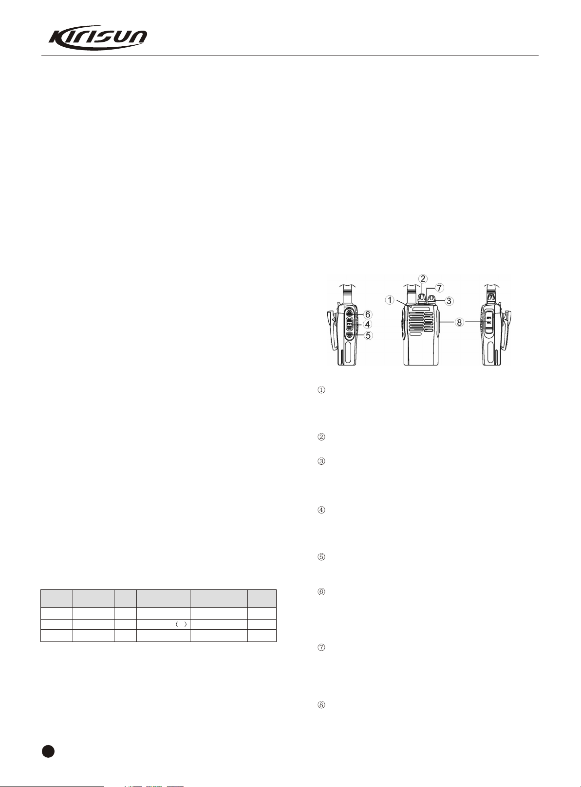
LED Indicator
Lights red while transmitting; lights green while receiving a
signal.
Flashes red while in low battery power.
Channel Selector
Rotate to select channel 1-16.
Power/Volume Switch
Turn clockwise to switch on the radio.
Turn counterclockwise till a click is heard to switch off the radio.
Rotate it to adjust the volume after turning on the radio.
PTT (Push-to-talk)
To make a call, press and hold the PTT button, then speak into
the microphone in normal voice.
Release the PTT button to receive a call.
Monitor Button
Press to disable the SQUELCH, and release to enable the
SQUELCH again.
Channel Annunciation Button
Press it in standby state, and the channel number will be
annunciated. If press and hold this button, and at the same time
switch on the radio again, the type of voice annunciation of channel
number will be changed.
Emergency Button
Press and hold this button for over 2 seconds to activate
warning tone. Press it again to exit the emergency alert state.
Note: When warning tone sounds, all of the buttons are
disabled.
Microphone/Speaker Jacks
For connecting external Microphone/Speaker.
1
Page 4
PT4200 SERVICE MANUAL
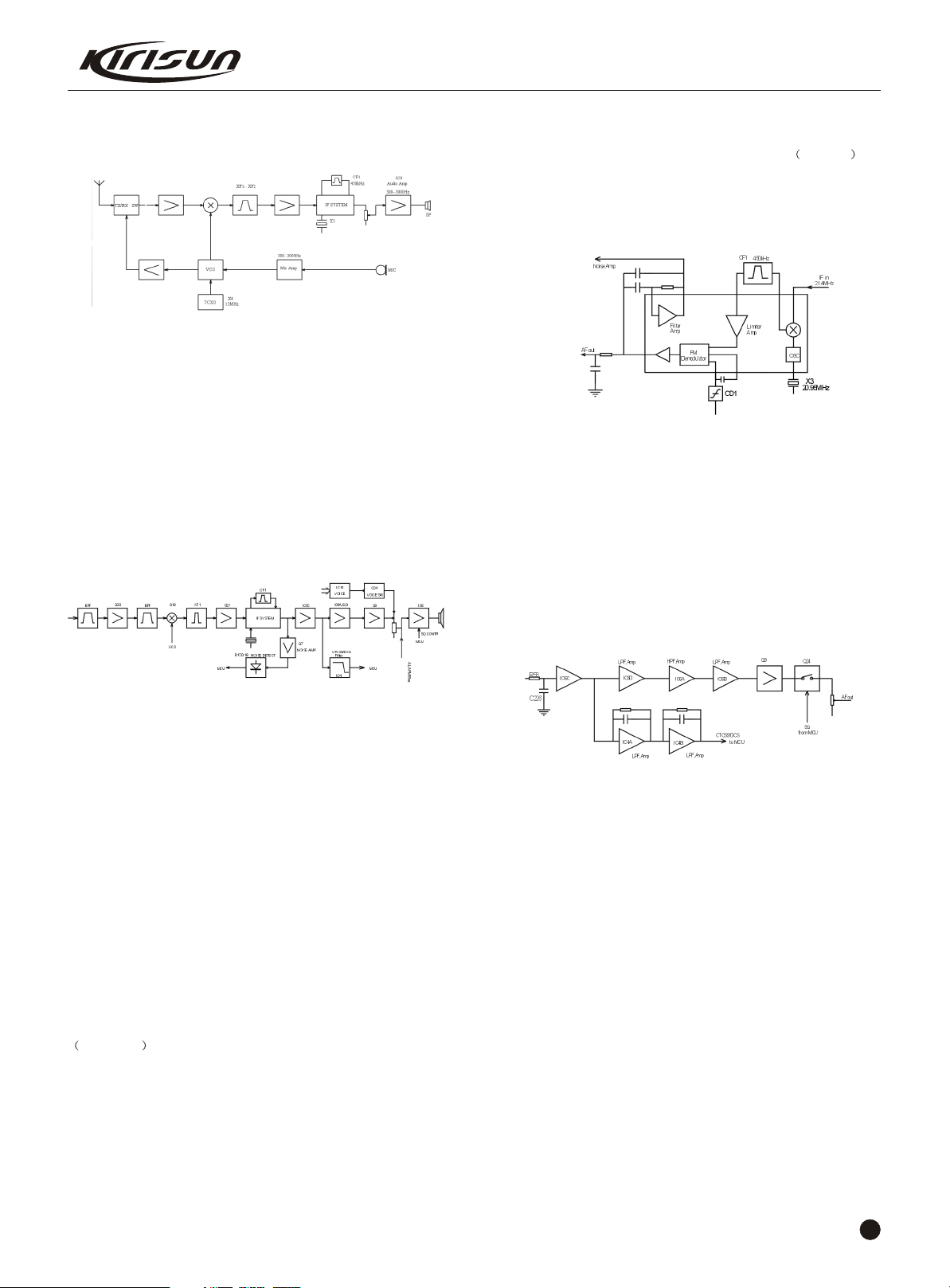
Chapter 3 Electrocircuit
3.1 Frequency Configuration
Figure3.1 Frequency Configuration
This radio adopts the 2nd Mixer, the 1st IF 49.95MHz, the 2nd
IF 450kHz.
The receiver's first local oscillation is generated by the
frequency synthesizer. The second local oscillation is generated by
the crystal oscillator.
The transmitter signals are generated by frequency synthesizer.
The reference frequency of frequency synthesizer is generated
by TCXO.
3.3 Receiver (RX)
IC5 inner circuit and X3 (49.5MHz) compose the 2nd local
oscillator. The 2nd local oscillation (49.5MHz) and the 1st IF signal
(49.95MHz) are mixed at IC5 to generate the 2nd IF 450MHz .
After the 2nd IF signal is amplified and its amplitude is limited at
IC5, and then filtered at porcelain filter (CF1,450kHz), IC5
demodulates and sends out audio signals.
Figure 3.3IF System
Receiver Audio Signal Processing
IC6 and its peripheral circuit compose the receiver audio signal
processing circuit. IC5 sends audio signals to IC6-C for
amplification, and then to IC4 (CTCSS signaling filtering circuit) and
IC6-D. After the signals are amplified, de-emphasized, filtered at
IC6 and other cells, the HF (high frequency) and LF (low frequency)
will be eliminated, and the remaining 300-3000Hz audio is sent to
Q9 for amplification and then to volume potentiometer for
adjustment and finally sent to the audio amplifier (Ic8).
Figure 3.2 Receiver Illustration
The Receiver Front Terminal
Signals from the antenna pass through the RX/TX switch (D1,
D2, D4, D5); and then undesirable out-of-band signals will be
filtered out at the band pass filter (BPF) consisting of C227, L8, L15,
C70, C126, C218, L9, C217, L10, C127; then signals are amplified
at the low noise amplifier (LNA) consisting of Q20 and its peripheral
components.
The output from the LNA passes the BPF consisting of L5, L6,
L7, C228, C124, and C132 for filtering and then is sent to the first
grade frequency mixer (Q19).
MCU produces output voltages and alters the capacitance of
the variable capacitor diodes D21, D22, D23, D24, D26, D30 to
control the center frequency of the band-pass filter.
The First Frequency Mixer
After mixing the receiving signals and the first local oscillation
signals from the frequency synthesizer, the 1st IF signals
49.95MHz are generated. The first IF signals pass the crystal
filter (XF1, XF2) , which will filter the signals of adjacent channel
and those out of band.
IF Circuit
The 1st IF signals from the crystal filter are amplified at the first
IF amplifier (Q21), and then are sent to the IF processing IC (IC5,
MC3361). The IF IC consists of the 2nd frequency mixer, the 2nd
local oscillator, IF amplifier, limiter, phase frequency detector, and
noise amplifier.
Figure 3.4 Receiver Audio Processing
Squelch Circuit
Demodulation output from IC5 is sent to the selection frequency
noise amplifier, which consists of IC5 inner noise amplifier and
C107, R124, R152, C33, and C35, to be filtered off the noise. After
being amplified at Q7, noise is sent to D17 and D18 for wave
checking and then sent to MCU, which determines the noise
volume to control the squelch.
Audio Amplifier
IC8 and peripheral components construct the audio amplifier.
Receiving audio signals, voice indication signals, indication tone
signals and warning tone signals are collected for audio
amplification to drive the speaker. Warning tone has no volume
control.
When AFCO is at the high level, Q37, Q8, Q33, and Q38 will be
connected, and IC8 starts working and voice comes out from the
speaker.
Q36: Receiving audio signal switch
Q35: Warning tone switch
Q25: Indication tone switch
2
Page 5
PT4200 SERVICE MANUAL
CTCSS Signal Filtering
The IC5 demodulated output audio signals may contain CTCSS
(continuous tone coded squelch system) and DCS (digital coded
squelch). The frequency spectrum of CTCSS/DCS is 2-250Hz. The
filtering circuit constructed by IC4 can filter out the signals out of the
CTCSS/DCS frequency spectrum to ensure MCU to decode
CTCSS/DCS more precisely.
3.2 Transmitter (TX)
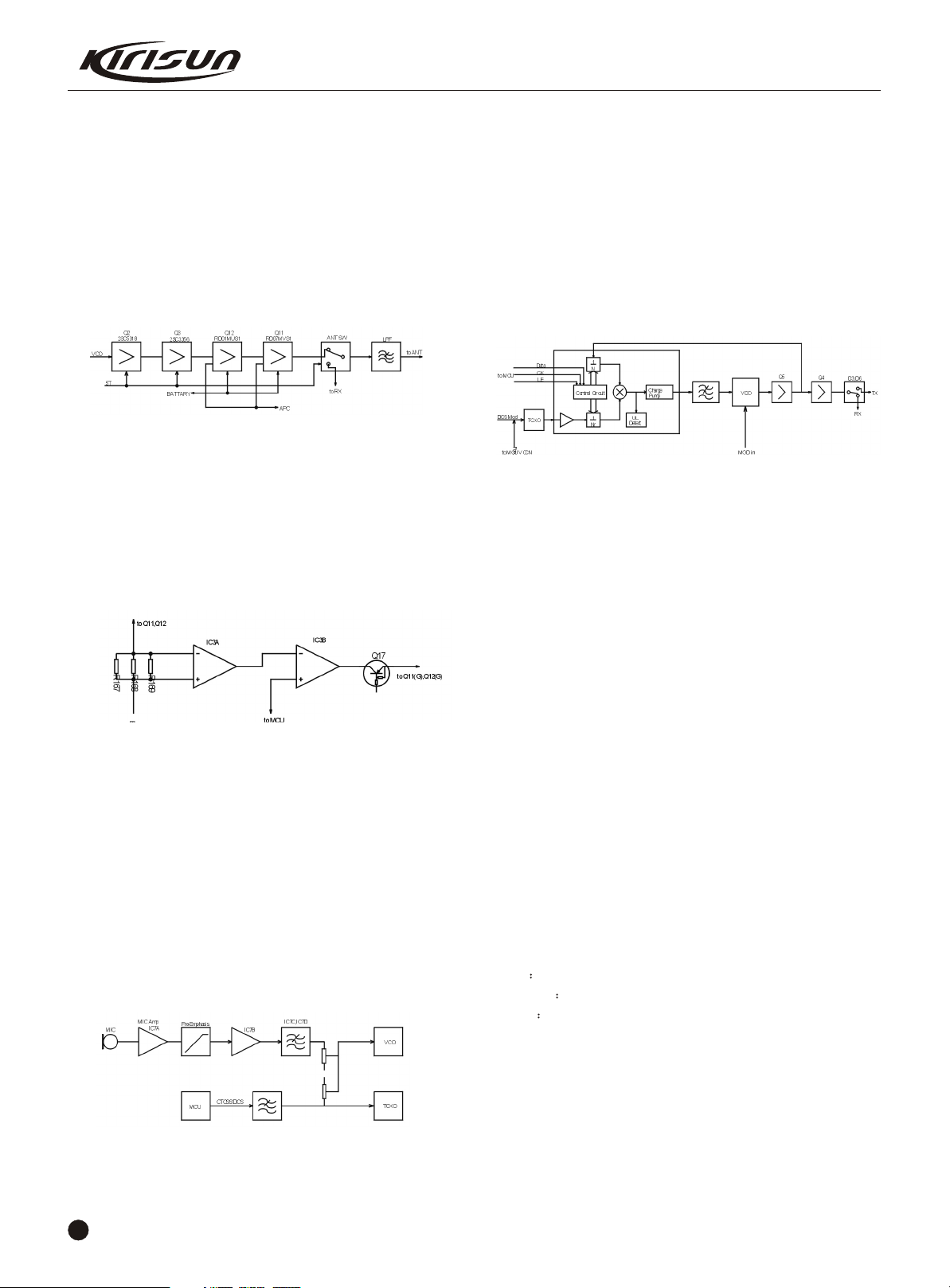
Transmitter Amplifier
Figure 3.5 Amplifier and Antenna Switch Diagram
The modulated signals from VCO are amplified at Q2, Q3, and
Q12 and then are sent to Q11 for amplification. Q11 output power:
4.5W.
The Q11 and Q12 gate offset is controlled by APC circuit.
Changing gate-offset voltage can control the transmitter output
power conveniently.
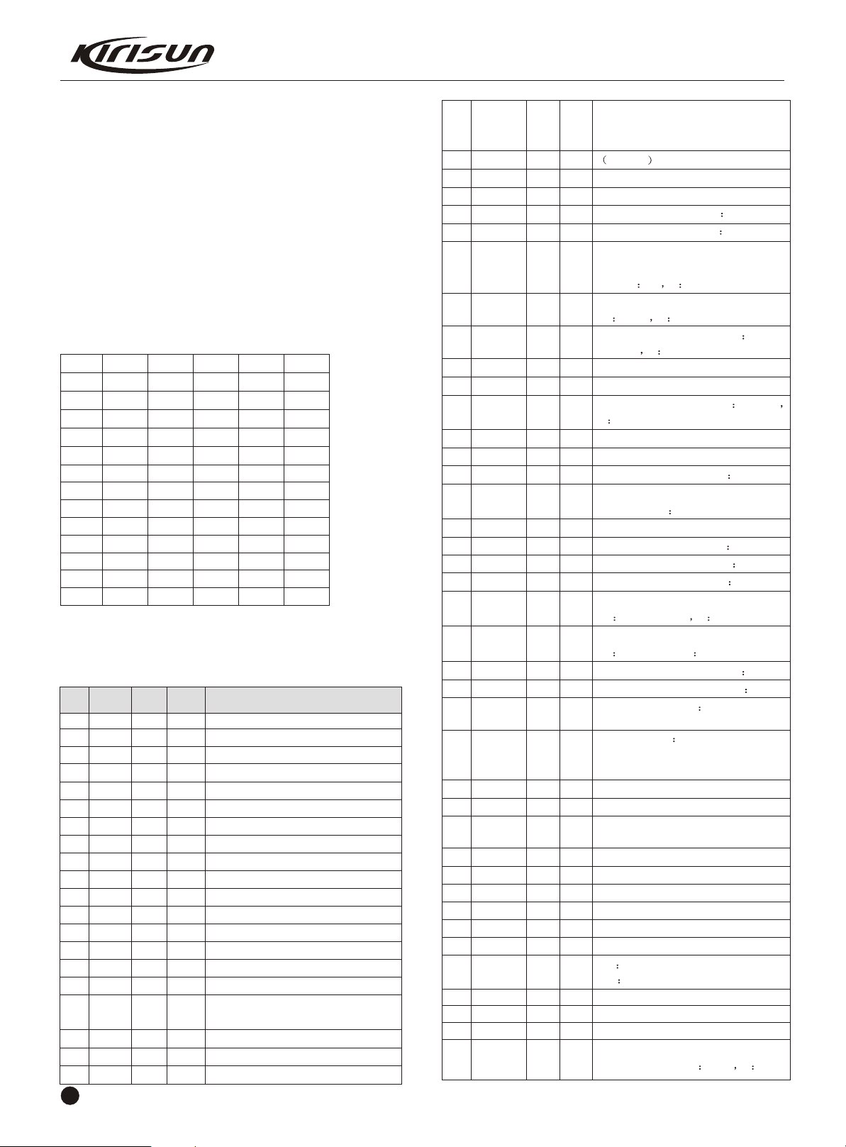
APC (Auto Power Control)
Figure 3.6 APC Circuit
R167, R168, and R169 are the amplifier current checker; IC3A
is the sample amplifier of the amplification current; IC3B is the
power comparison amplifier.
If the transmitter output power is too big, the amplifier current
will increase, IC3A output will mount, IC3B output voltage decrease,
the offset voltage added to Q11 and Q12 will decrease, and then
the transmitter output power will decrease. Vice versa, such can
ensure steady transmitter output power in different working
circumstances.
MCU changes the input power to IC3B to set the power.
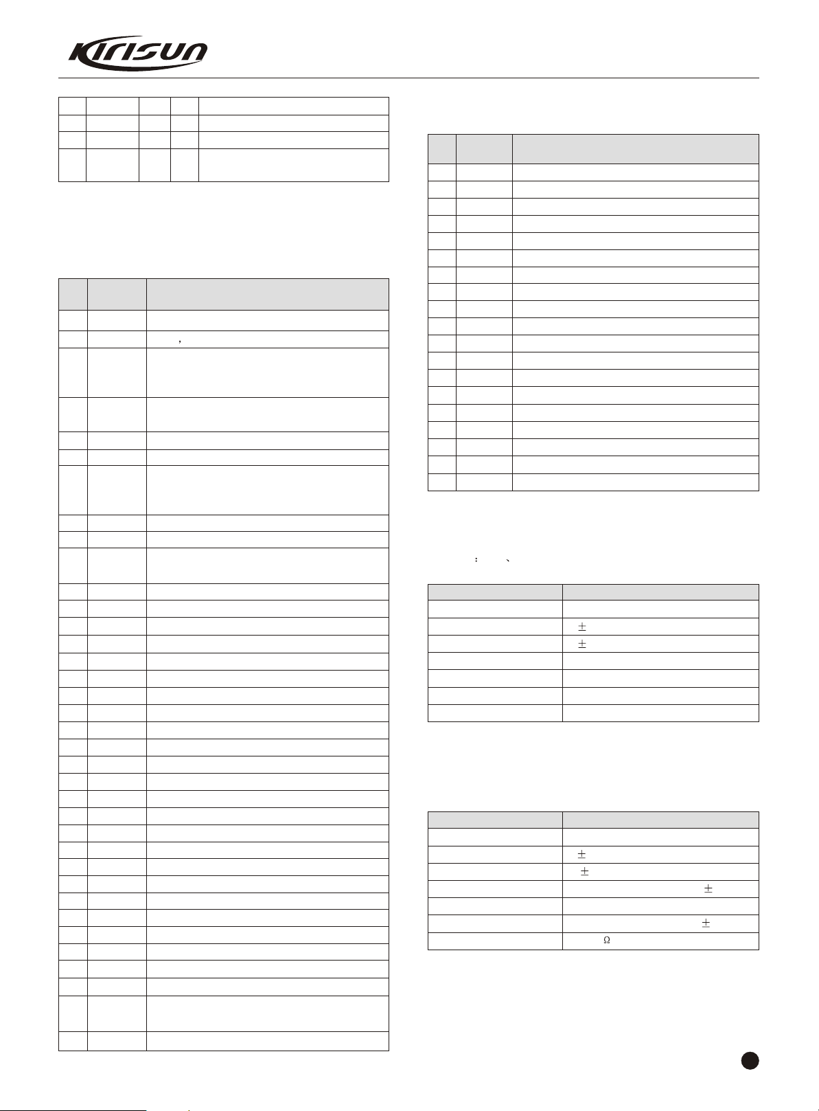
Transmitter Audio Signal Processing
amplified, the amplitude of them is limited, and are filtered, they are
sent to VCO together with CTCSS/DCS for modulation.
D13, D308, and Q24 constitute AGC circuit which decreases
signal amplitude to avoid signal distortion when MIC signal is too
big.
Q34 is the power switch of audio processing circuit. It supplies
power to IC7 only when in transmitting and it is controlled by MCU.
J2 is the external MIC socket. When external MIC is used, the
inner MIC will cut off automatically, but PTT will remain activated.
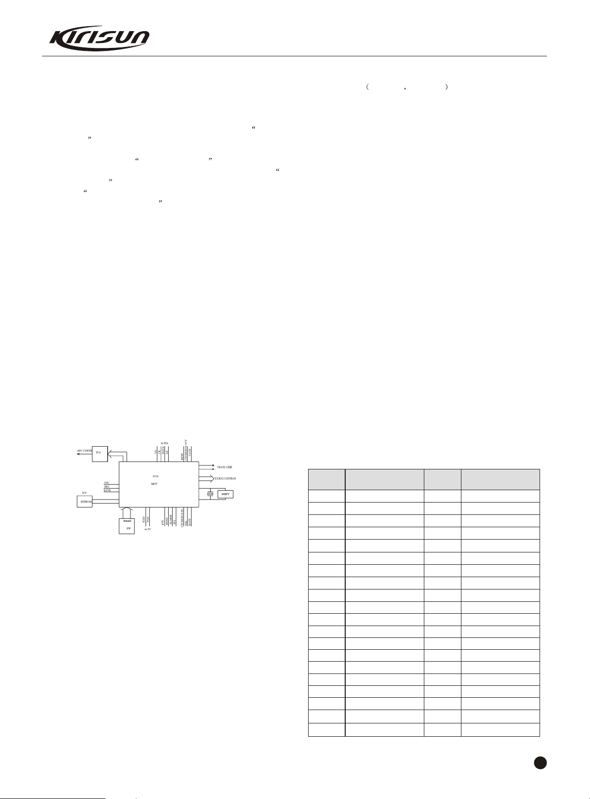
3.3 Frequency Synthesizer
Figure 3.8 Frequency Synthesizer
The radio adopts PLL (Phase Locked Loop) frequency
synthesizer.
The frequency synthesizer consists of standard oscillator,
voltage controlled oscillator (VCO), programmable frequency
demultiplier, phase comparator, and low pass filter.
Q14, L30, C120, C88, C142, C180, D8, and D9 constitute RX
VCO. D12 is the modulation circuit of VCO.
ICI (MB15E03) is PLL integrated circuit, including
programmable reference frequency demultiplier, programmable
swallowing frequency demultiplier, phase comparator, and charge
pump.
R244, c193, R202, R40, C207, R141, C205, R2, and C204
construct the low pass filter.
The standard frequency is supplied by X4 (TCXO, 13MHz).
The standard frequency fromTCXO (Temperature Control
Transistor Oscillator) are demultiplied by the programmable
reference frequency demultiplier at IC1 to acquire 5kHz or 6.25kHz
reference frequency (controlled by MCU according to the preset
channel frequency).
The oscillation frequency from VCO is sent to IC1, and
demultiplied by swallowing frequency demultiplier and compared
with reference frequency to acquire the error signals. Then pass the
low pass filter and are sent to VCO to change VCO oscillation
frequency to the preset value, and then VCO is locked.
N=FVCO/FR
N Frequency demultiplication times
FVCO VCO oscillation frequency
FR Reference frequency
Figure 3.7 Transmitter Audio Circuit
IC7 and the peripherals components construct the transmitter
audio processing circuit. After the audio signals from MIC are
3
Check Loss of Lock: When PLL is in loss of lock, IC pin14
sends out low level signals to MCU, which controls the transmitter
not to transmit and initiate warning tome.
Q6: Power filter to supply more pure power to reduce the noise
of the frequency synthesizer.
3.4 Voice Indication Circuit
The radio features voice indication, which is very useful at night
or in the environment of dim light.
Page 6
IC15 is a voice memory chip which stores the voice indication of
channels, and every time you change the channel, the speaker will
sound voice annunciation of the current channel number. Press
voice annunciation key will repeat the voice annunciation of the
current channel number.
If the voice annunciation function has been set, press voice
annunciation key in the stand by mode and the speaker will
sound voice annunciation of the current channel number. If turn on
the radio again with the voice annunciation key pressed, the
voice type will be changed. Repeat turning on the radio with the
voice annunciation key pressed, the voice type will change in the
sequence Chinese Male--- English Male--- Chinese Female --English Female ---- No Indication .
3.5 Power Supply
The radio is equipped with 7.4V, 1200mAh Li-Ion battery. The
battery supplies power directly to the transmitter amplifier circuit
(Q11, Q12) and the receiver amplifier (IC8). The power supply of
other circuits is the regulated 5V power.
IC12: 5V low voltage difference, micropower regulator, together
with Q10, and Q30 supply big current 5V power to the whole radio.
Q29: 5T switch, controlled by MCU.
5T: Supplies power for the front terminal of the transmitter.
Q31: 5R switch, controlled by MCU.
5R: Supplies power for the receiver RF amplification, mixing, IF
processing, audio signal processing.
Q32: 5C switch, controlled by MCU
5C: The 5V power controlled by power saving supplies power
for the frequency synthesizer.
3.6 MCU
PT4200 SERVICE MANUAL
Memorizer E2PROM AT24C08
Memorizes the radio channel data, CTCSS/DCS data, and
other data of function setting and parameter adjustment.
CTCSS/DCS Encoding and Decoding
CTCSS/DCS signals generated by MCU (output form pin5) are
filtered at R155, R156, C242, and C243, and then sent to VCO and
TCXO for modulation.
CTCSS/DCS signals from the receiver are sent to MCU(pin1)
for demodulation. MCU determines whether the signals contain the
same CTCSS/DCS as that set on the radio and decides whether to
turn on the speaker.
Power Adjustment
MCU P56 output is sent to APC part to control the transmitter
output power.
CTCSS
CTCSS (continuous tone control squelch system) is a squelch
control system modulated on carrier wave with continuous subaudio
frequency as pilot frequency. If a channel is set with CTCSS, only
when both the CTCSS of the receiver and that of the transmitter are
identical, communication is available, which avoids interference of
other signals.
39 groups of standard CTCSS frequency is available on the
radio, see Table 3.1.
CTCSS signals generated by MCU pass the low pass filter
consisting of RC to be filtered off the high frequency over 300Hz
and then are sent to VCO for modulation.
Figure 3.9 MCU Diagram
MCU controls the working of each unit of the radio to realize all
the radio functions.
Connects with the PC
Accesses the radio status data
Controls PLL to generate the receiving and transmitting local
oscillation frequency.
Accesses the current channel status.
Controls the LED status indication
Controls the power supply of each location
Checks the action of each function key
Generates CTCSS signals
Generates DCS signals
DCS decoding
Squelch check and control
Controls the content of voice indication
Table 3.1 CTCSS Frequency Table
.
No
FREQUENCY
(Hz)
1 67.0 131.8
2 69.3 136.5
3 71.9 23 141.3
4 74.4 24 146.2
5 77.0 25 151.4
6 79.7 26 156.7
7 82.5 27 162.2
8 85.4 28 167.9
9 88.5 29 173.8
10 91.5 30 179.9
11
12
13
14
15
16
17
18
19
20
94.8
97.4
100.0
103.5
107.2
110.9
114.8
118.8
123.0
127.3
No
.
21
22
31
32
33
34
35
36
37
38
39
FREQUENCY
(Hz)
186.2
192.8
203.5
210.7
218.1
225.7
233.6
241.8
250.3
4
Page 7
PT4200 SERVICE MANUAL
DCS
DCS (digital code squelch) is a kind of continuous digital code
modulated with voice signals on carrier wave to control squelch.
83 groups of standard codes (positive and inverse code) are
available. See table 3.2.
DCS signals generated by MCU (PWM wave shape) pass the
low pass filter to be filtered off the high frequency over 300Hz and
then are sent to VCO and TCXO for modulation. VCO modulates
the high frequency of DCS signals; TCXO modulates the low
frequency of DCS signals.
CTCSS/DCS signals from the receiver are sent to MCU for
modulation. MCU determines whether the DCS encoding of the
receiving signals is identical with that set on the radio and decides
whether to turn on the speaker.
Table 3.2 DCS Encoding List
023 114 174 315 445 631
025 115 205 331 464 632
026 116 223 343 465 654
031 125 226 346 466 662
032 131 243 351 503 664
043 132 244 364 506 703
047 134 245 365 516 712
051 143 251 371 532 723
054 152 261 411 546 731
065 155 263 412 565 732
071 156 265 413 606 734
072 162 271 423 612 743
073 165 306 431 624 754
074 172 311 432 627
3.7 Semiconductor Component
MCU Description
Table 3.3 Microprocessor (M38034) Port Description
Port
No
.
1 TI P1 I
2 BUSY P2 I Busy s ignal in put
3 BATT P3 I Ba ttery vo ltage check
4 ALARM P4 I Alarm key check
5 TO P5 O QT/DQT output
6 BEEP P6 O Beep output/warning tone output
7
8
9
10
11
12
13
14
15
16
17 SELF P17 I Self programming
L: Model setting mode
18 CNVSS P18 I Connect 10K resistor with VSS
19 RST P19 I R e set i nput
20 INT0 P20 I P o w er ch eck in put
Name
PF1
ENC0
ENC2
ENC3
ENC1
NC
PTT
TXD
RXD
MONI
Pin
Name
I/O
QT/DQT signal input
P7 I Voice indication key check
P8 I Encoding input
P9 I Encoding input
P10 I Encoding input
P11 I Encoding input
P12 I Not used
P13 I [PTT] key input, connected with RXD
P14 O RS-232C input
P15 I RS-232C input
P16 I [MONI] key input
FunctionPin
5
21 ENC P21 I
-SEL
Connect the pull down resistor with
VSS .
22 XIN P22 I 7.3MHz Osc illator
23 XOUT P23 O
24 VSS P24 I
25 SHIFT P25 O
26 PABC P26 O
27 OSCSI P27 I
28 WNTC P28 O Wide/Narrow band contro l
H Wide L Narrow
29 PS P29 O PLL p ower s aving co ntrol H No rmal
working L Power saving
30 SDA P30 I/O EE PROM data wire
31 SCL P31 O EE PROM cloc k wire
32 UL P32 I PLL unlock che c k pin H Locked
33 DT P33 O PL L data output
34 CK P34 O PL L clock output
35 LE P35 O PLL IC en abl i n g pin H L atched
36 5MC P36 O Power control excep t CPU and
EEPROM L Open
37 AFCO P37 O
38 RX P38 O TX/RX VCO Se l e c tion H Rece iving
39 GLED P39 O Gree n indicato r contro l H Ligh t
40 RLED P40 O Re d indicato r contro l H Light
41 SAVE P41 O Battery power saving c o ntrol
H Power supply L Power saving
42 MUTE P42 O Squelc h contro l
H L Audio squelch
43 5RC P43 O
44 5TC P44 O
45 W588C P45 O
46 AC P46 O
47 DAOUT1 P47 O
48 DAOUT0 P48 O
49 DAOUT7 P49 O
50 DAOUT6 P50 O D/A output6
51 DAOUT5 P51 O D/A output5
52 DAOUT4 P52 O D/A output4
53 DAOUT3 P53 O D/A output3
54 DAOUT2 P54 O D/A output2
55 NC P55 O Not used
56 APC P 5 6 O
RX BPF tuning output
57 VCC P57 I CPU pow er 5V input
58 VREF P58 I Connected with VCC
59 AVSS I Conn ecte d with VSS
60 IF_SEL
resistor with VSS H 49.95 L 21.4
P59
P60
Encoding switch selection.
Earthing
Clock frequency shift H Open
Final power supply H Open
VCO crystal selection.
Connect the pull down resistor with
VSS H 13 L 16.8
L Loss of lock
Audio amplification power H:Open
Mic squelch
eceiving power control L Open
R
Transmitter power control H Open
Voice indication H Voice
annunciation of channel
Alert control H Control by voice
volume.
It must be in low battery
when in emergency alert state
D/A output 1
D/A output 0
D/A output 7 frequency regulated
output VCCN
TX Auto power contro l outpu t
I
IF selection. Connect the pull down
level
.
Page 8
PT4200 SERVICE MANUAL
61 BUSY_V P61 I Voice indication of circuit busy check
62 DATA_V P62 I/O Voice indication data
63 SCLK_V P63 I/O Voice indication clock
64 NC Not used
3.4 Semiconductor Function Description
Posi
Type Function Description
IC1 MB15E03 Frequenc y synthesizer
IC4 NJM2904 APC Voltag e comparison , driv e
IC5 MC3361 Receiver' s 2n d loca l oscillation , 2n d I F
IC6 NJM2902 Receive r demodulatio n signa l
IC7 NJM2902
IC8 KIA6278F
IC9 AT24C08
function setting parameter,
IC10 M38034
IC11 PST9140NR
IC12 HT7150-1 Lo w voltag e differenc e, lo w powe r
IC15 W588A080 Voic e storag e I C
Q2 2SC5108 Transmitt er 1 st amplification
Q3 2SC3356 Transmitt er 2n d amplificatio n
Q4 2SC5108 VC O bufferin g amplifi er
Q5 2SC5108 VC O bufferin g amplifi er
Q6 2SC4617 VC O pow er filter
Q7 2SC4738 Nois e amplifier
Q9 2SC4617 Receiv er aud io signa ls amplification
Q10 2SC1623 5 V regulate d outp ut curre nt stretch er
Q11 RD07MVS1 Transmitter fina l pow er amp lifier
Q12 RD01MUS1 Transmitter pow er amp lifier driv e
Q17 DTA144EE AP C outp ut switc h
Q19 3SK318 Th e 1 st frequenc y mix er
Q20 3SK318 Receiv er H F amplifi er
Q21 KTC4082 Th e 1 st IF amplifier
Q22 DTC144EE Re d LE D driv e
Q23 DTC144EE Gree n LE D drive
Q24 2SK1824 Voic e indicatio n switch
Q26 DTC144EE 5 C switc h
Q29 KTA1298 5 T switc h
Q30 KTA1298 5 V regulate d outp ut curre nt stretch er
Q31 KTA1298 5 R switc h
Q32 KTA1298 5 C switc h
Q34 DTA144EE Pow er switc h of M IC amplificatio n un it
Q35 2SK1824 Aud io outp ut switc h of receiver.
Q36 2SK1824 Receive r aud io outp ut switc h
P64 I
amp lificati on, amplitude limit,
demodulation, noise amplification
am plification, filtering
MIC amplification , amplitud elimi
Receive raudi o amplifie
E2PROM , memor ychanne l frequenc ydata ,
Debugging state parameters
MCU
MCU rese tcircu it
consumption, and regulator
Cut off when in emergency alert state.
filterin
t,
g
r
Table 3.5 Diode Function Description
Posi
Type Function Description
tion
D1 MA77 Trans mitter an tenna s witch diode
D2 MA77 Trans mitter an tenna s witch diode
D3 HSC277 VCO output switch
D4 HSC277 Antenna switch
D5 HSC277 Antenna switch
D6 HSC277 VCO output switch
D7 HSC277 5V regulated output current stretcher
D8 HVC376B VCO oscillation variable capacitance diode
D9 HVC376B VCO oscillation variable capacitance diode
D12 MA360 VCO modulation diode
D14 HZU5ALL APC output voltage-limiting diode
D15 MA2S111 Loss of lock check diode
D16 MA2S111 VCO power filtering accelerating diode
D17 1N4148 Noise detector
D18 1N4148 Noise detector
D20 LED Green Receiving indication
D25 MA2S111 APC individual diode
D28 LED Red Transmitting indication
D29 LED Green Receiving Indication
Table3.6 XF1 XF2 Crystal Filter Features
Item Specified Value
Nominal center frequency 49.95MHz
Transmission bandwidth 7.5kHz or bigger within 3dB
40dB Barrage bandwidth 20.0kHz or smaller
Pulse 1.0dB or smaller
Insertion loss 3.0dB or smaller
Guarantee attenuation 80dB or bigger within fo-910kHz
Terminal resistance ---
Table 3.7 CF1 LTVPC450EB Features
Item Specified Value
Nominal center frequency 450kHz
6Db bandwidth 3.5kHz or bigger
50dB bandwidth 12.5kHz or smaller
Pulse 2.0dB or smaller within f0 4kHz
Insertion loss 6.0dB or smaller
Guarantee attenuation 35.0dB or bigger within f0 100kHz
Terminal resistance 2.0k
6
Page 9
PT4200 SERVICE MANUAL
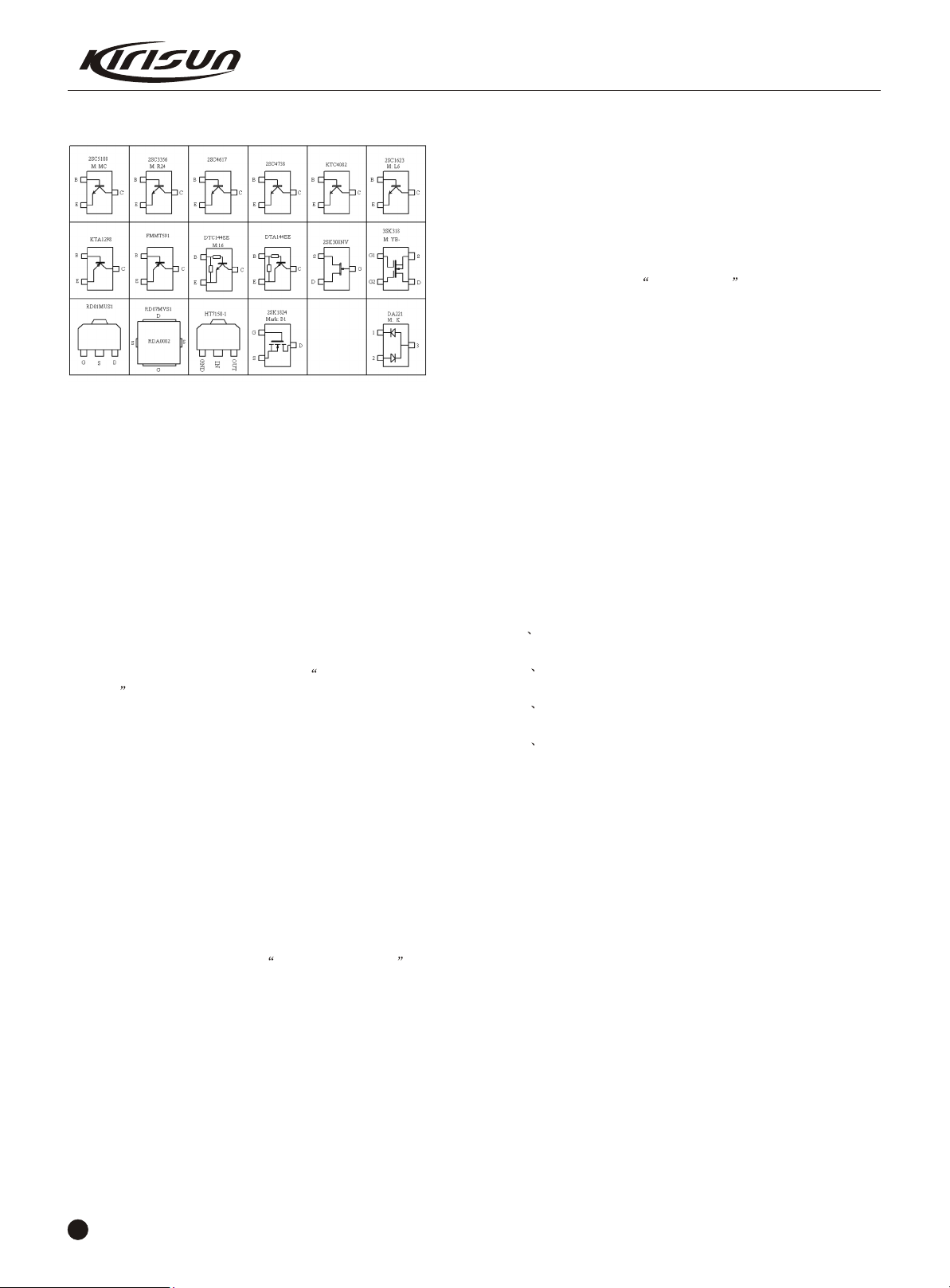
Figure 3.8 Semiconductor Component Packaging Illustration:
Chapter 4 Function Description and Parameter
Setting
4.1 Major Functions
4.1.1 16 Channels/15 Channels +Scanning Channel
The radio stores 16 channels including one scanning channel.
4.1.2 Scanning Function Control
If you switch the channel to channel 16, the radio is in the
scanning state. After starting scanning, it will pause when receiving
signals.
If you switch the channel to channel 1-15, the scanning function
is inactivated.
4.1.2.1 Carrier Wave Control Scanning
If the radio scanning setting is carrier wave control
scanning , switch the channel to channel 16 to set the radio in the
scanning working mode.
Each channel can be set the scanning added/deleted function
solely: if the setting is scanning added, the channel will be added in
the scanning list; if the setting is scanning deleted, the channel will
not be in the scanning list.
The radio starts scanning from channel 1 to 16 repeatedly in the
consequence of the scanning list. If signals are detected on a
channel ( if the channel is set with receiving signaling the carrier
wave must match the signaling), the radio pauses on that channel
and will restarts scanning 0.5~5 seconds (scanning delay time) after
the signals disappear.
If you switch the channel to channel 1~15, scanning is
inactivated.
4.1.2.2 Time Control Scanning
If the radio scanning setting is time control scanning , switch
the channel to channel 16 to set the radio in the scanning working
mode.
Each channel can be set canning added/deleted function solely:
if the setting is scanning added, the channel will be added in the
scanning list; if the setting is scanning deleted, the channel will not
be in the scanning list.
The radio starts scanning from channel 1 to 16 repeatedly in the
consequence of the scanning list. If signals are detected on a
channel (if the channel is set with receiving signaling the carrier
wave must match the signaling), the radio pauses on that channel
and will restarts scanning 0.5~5 seconds (scanning delay time) after
the signals disappear.
If you switch the channel to channel 1~15, scanning is
inactivated.
7
4.1.2.3 Priority Channel
You can set one channel in the scanning list as the priority
channel, which has the highest priority during scanning. The radio
scans the first non-priority channel in the canning list and then
scans the priority channel, the next non-priority channel in the
scanning list, and then the priority channel again. It goes on
scanning in such sequence.
4.1.2.4 Revert Channel
If you press PTT button when the radio is in scanning state, the
radio will transmit on the revert channel , which has 6 types:
Selected channel: The first channel in the scanning list.
Selected channel + current channel: If the radio is in the state of
scanning pause, it will transmit on the current communication
channel. Otherwise it will transmit on the first channel in the
scanning list.
Priority channel: The radio will always transmit on the priority
channel set in the scanning list when pressing PTT.
Priority channel + current channel: If the radio is in the state of
scanning pause, the radio will transmit on the current
communication channel. Otherwise it will transmit on the priority
channel in the scanning list.
Last called channel: The last channel that received signals.
Last called channel + current channel: If the radio is in the state
of scanning pause, the radio will transmit on the current
communication channel. Otherwise it will transmit on the last called
channel.
The current communication channel is the channel on which the
radio pauses in the 4 following situations:
1 When the radio receives signals and does not restart
scanning, the radio will stay on the current channel.
2 The radio will stay on the current channel during 0.5~5
seconds (scanning delay time) after signals disappear.
3 The radio will stay on the current channel when pressing
the PTT during scan.
4 After releasing the PTT to end transmitting, during the
preset transmitting dwell time, the radio will stay on the current
channel. After the preset transmitting dwell time 0.5~5 seconds, the
radio will restart scanning again.
4.1.2.5 Retrace Period
If the priority channel has been set in the scanning list and
retrace period is also set, when the radio receives signals on a nonpriority channel and pauses scanning, it will retrace the priority
channel in a certain period (0.3~5s). If signals are detected on the
priority channel, it will stay on the priority channel; if no signal is
detected on the priority channel, it returns to the original channel it
stays on.
4.1.3 CTCSS/DCS
CTCSS/DCS can realize selective calls and group calls. On the
same channel, only the two parties whose CTCSS/DCS are
identical can communicate. CTCSS/DCS signaling code on the
channel is preset.
4.1.4 TOT
The purpose of the time-out timer is to prevent any single
person from overlong using a channel to transmit and affecting the
whole group communication.
If the radio transmits longer than the preset TOT time limit, the
radio will stop transmitting and warning tone sounds. To stop the
warning tone, release the PTT button. Press the PTT again you can
resume transmitting.
4.1.5 Auto Power Saving
When no signals are being received or no operations are being
Page 10

PT4200 SERVICE MANUAL
conducted for over 10 seconds, the battery power saving will be
activated. When it is receiving signals or in operating state, battery
power saving is inactive.
4.1.6 Low Battery Warning
When the battery power appears low, the indicator flashes. If
the battery power is lower than the preset value during transmitting,
the status indicator flashes red. When the speaker sounds warning
tone, the radio will stop transmitting.
4.1.7 Monitor
When no signals are being received, the radio squelch circuit
mutes the speaker.
Press the MONI key to cut off the squelch control circuit, and
you will hear noise from speaker (no mater whether there are
signals). Such operation is very useful when you want to adjust
voice volume or receive weak signals (to avoid voice intermittence
when in weak signals).
When you press the MONI key, the green indicator lights, and
the radio is in the state of monitoring.
4.1.8 Busy Channel Lockout
If busy channel lockout has been activated, transmitting
signals is prohibited on the busy channel. If you press the PTT to
transmit on the busy channel, the speaker will sound busy channel
lockout tone, and you cannot transmit signals.
4.1.9 PC Programmable
You can program the radio functions and adjust some
parameters by PC programming software KSP20.
4.1.10 Wired Clone
The radio can transfer the stored data to another radio of the
same mode by a specified cable.
4.1.11 Squelch Level Selection
The purpose of the squelch is to mute the speaker noise when
no signals are received or the signals are weak. When the squelch
is activated, you can hear noise from the speaker; when the
squelch is inactivated, you will not hear noise form the speaker.
Selecting the squelch level is to select which the signal strength
level is strong enough to enable the squelch or weak enough to
disable the squelch. Over high squelch level will make the radio
unable to receive signals efficiently when signals are weak; over low
squelch level will make the radio communication affected by noise
or other irrelevant signals. The squelch level has 0-9 options.
4.1.12 Beep Tone
This option controls power on tone, channel busy tone and TOT
tone.
4.2 Parameter Setting (PC Mode)
The radio parameters have been programmed in the factory.
The user can program the radio parameters such as working
frequency, channels, CTCSS/DCS, auto scanning. We designed a
user friendly and convenient Chinese/English programming
software KSP20 for users to set parameters on the radio. The
programming steps are as follows:
a.Install the programming software KSP 20 on the computer.
b.Connect the radio to the computer serial port with the
specified programming line (KSPL02). See Figure 4.1
a.Turn on the computer power.
b.Turn on the radio power.
c.Click the KSP20 program to run the programming software.
d.Click the Tools in the KSP20 pull-down menu, and click
Read Data to read the radio parameters into the computer;
click Write Data to transfer the PC programming parameters
into the radio.
e.You can program the following parameters with the KSP20
software.
1) The RX and TX frequency of each channel.
2) The receiving and transmitting signaling of each channel.
3) Busy channel lockout option.
4) TOT
5) Squelch level option.
6) Power saving option.
7) Beep tone option.
8) Monitor mode option.
9) Scan mode option.
10) Scan the revert channel option.
11) Scan the priority channel option.
For more details, please refer to the Help in the KSP20
software.
Notice:
1) Turn off the radio before connection.
2) When the radio is being read data, the indicator lights green
and it's prohibited to press the PTT button; when the radio is being
written data, the indicator lights red.
3) Before the first time editing, you should read data form the
radio and backup the data.
4) If the radio cannot work normally after being written in with
the editing data, open the data backup and rewrite the backup into
the radio.
5 )Model information is important radio data and is prohibited to
modify.
6) After programming, you need to turn on the radio power
again to make the radio resume the normal work.
4.3 Computer Test Mode:
Connect the radio to the radio communication port with the
specified programming line (KSPL02). See Figure 4.1.
Warning: Before enter the computer test mode, connect a HF
load of 50 to the radio antenna connector or connect the radio to a
comprehensive test device.
Under the computer test mode, you can modify the following
parameters with KSP20 programming software:
1) Frequency tuning;
2) Transmitting power;
3) Low voltage threshold;
4) The 9th squelch level;
5) The 3rd squelch level;
6) Sub-audio wide band modulation degreed;
7) Sub-audio narrow band modulation degreed;
8) Wide band sub-audio center.
PC
(RS232 Serial
Port)
Programming
Line (KSPL02)
Radio
(Speaker/ Mic
Socket)
4.4 Wired Clone (It can be prohibited by programming
software)
When the wired clone function is activated, the radio can enter
the wired clone mode. After entering the wired clone mode, the
8
Page 11

PT4200 SERVICE MANUAL
radio will not exit it automatically and you have to turn on the radio
again to enter the user's mode. Operating steps are as follows:
1) Turn on the radio with the MONI key pressed, and 2 seconds
later the red light flashes twice and two beep tones sound, and then
the radio enters the wired clone mode.
2) Press the PTT button on the host radio to activate/inactivate
the wired clone mode on the sub radio. But the wired clone mode of
the host radio will not be changed. When pressing the PTT button,
the green light flashing twice and one beep mean to activate the
clone mode; the red light flashing twice and two beeps mean to
inactivate the clone mode. When entering clone mode, the default
setting of the sub radio receiving data is to prohibit wired clone
mode.
3) Press the MONI key, red light flashes, and it starts cloning.
After cloning is finished, the red light turns dim.
Note: You can activate/inactivate the wired clone mode. Short
circuit the two SELF terminals, enter the model setting mode and
then the manually adjustment function and wired clone function will
become active automatically. If you press the MONI key at this
moment, the wired clone function will be prohibited.
You can also activate/inactivate the wired clone mode by PC
programming software.
If the wired clone function has been prohibited, it cannot enter
the wired clone mode. The wired clone mode has been prohibited in
the factory.
The cloning data includes all the data in 4.2 Parameter
Setting but the adjustment parameters in 4.3 Computer Test
Mode .
Cloning Line
Host Radio
Sub Radio
5.2 Removing and Installing the Belt Clip
To remove the belt clip, use your nail or a tool to lift the metal
spring piece in the belt clip from the topside, and then pull the belt
clip away from the radio.
To install the belt clip, match the upper head of the belt clip with
the glides on the rear of the battery, and then press the belt clip
downwards to lock it in place. (See Figure 5.4)
Figure 5.4
5.3 Removing the Casing from the Chassis
1) Remove the knobs;
2) Remove the two knob nuts and the antenna nut;
3) Remove the two cross head screws that fix the top cover at
the top;
4) Remove the two cross head screws that fix the aluminum
alloy frame at the bottom;
5) Pull the aluminum alloy frame out of the casing.
See Figure 5.5
Chapter 5 Service Assemble and Disassemble
The radio is a precision communication equipment. Please be
careful when assemble or disassemble the radio during service.
5.1 Removing and Installing the Battery
To remove the battery, push the latch upwards and remove the
battery away from the radio. (See Figure 5.1)
Figure 5.1
To install the battery, match the tow bulges at the bottom of the
battery with the corresponding grooves at the radio aluminum alloy
frame and insert it in. Then press the upper end of the battery till the
latch secure.
Figure 5.5
5.4 Remove the Chassis from the Main Board
1) Remove the screw of from the PCB;
2) Melt the solder at the antenna point with a electric soldering
iron and take off the main board;
3) Take away the two screws and the antenna connector.
See Figure 5.6.
Figure 5.2
9
Figure 5.3
Figure 5.6
Page 12

5.7 Exploded View
41
42
43
44
40
39
38
37
36
35
34
33
32
31
21
30
20
PT4200 SERVICE MANUAL
29
28
27
26
25
24
23
22
18
17
16
15
19
NO.
MATERIAL NO.
21
202-000558-009
20
204-006800-006
19
202-000558-001
18
201-000558-008
17
202-000558-003
16
201-000558-002
15
201-000558-003
14
203-003208-009
13
203-000558-002
12
203-000558-001
11
202-000558-004
10
202-000558-005
9
201-000558-009
8
204-000558-001
7
121-100000-007
6
201-000558-001
5
401-0101E1-057
4
203-000558-004
3
202-000558-002
2
201-000558-004
1
401-0101E1-058
DECRIPTION
MIC CAP
MIC WASHER
MIC COVER
EMERGENCY BUTTON COVER
EMERGENCY BUTTON
VOLUME KNOB
CHANNEL KNOB
KNOB CIRCLIP
SWITCH NUT
ANTENNA NUT
arial
arial
LIGHT PIPE
SPEAKER WATERPROOF NET
SPEAKER
FRONT COVER
LOGO LABLE
SPEAKER SPRING
PTT BUTTON
PTT BUTTON FRAME
MODEL LABLE
QTY
1
1
1
1
1
1
1
2
2
1
2
1
1
2
1
1
1
2
1
1
1
44
204-000558-003
43
301-20080G-001
42
401-0201C1-006
41
204-000558-002
40
301-25060J-001
39
201-000558-014
38
203-000558-005
37
201-000558-005
36
203-003208-004
35
203-004200-001
34
204-000558-005
33
203-000558-007
32
202-000558-007
31
202-003208-007
30
302-17040G-001
29
203-003208-002
28
202-000558-008
27
201-000558-007
26
202-000558-006
25
204-003208-005
24
204-000558-004
23
22
301-20040G-001
14
13
12
11
10
9
8
7
6
5
4
3
2
1
AL LABLE
M2 SCREW
AL LABLE
WATERPROOF LABLE
M2.5 SCREW
PUSH FASTENER
PUSH FASTENER SPRING
TOP COVER
arial
Aluminum bracket
AL ALLOY LABLE
ANTENNA HEAD
WATERPROOF WASHER
INSULATING WASHER
M1.7 SCREW
arial
POSITIVE TERMINAL WASHER
POSITIVE TERMINAL FRAME
WASHER
WASHER
WASHER
PCB BOARD
M2 SCREW
1
2
1
1
2
1
1
1
1
1
1
1
1
1
1
1
2
1
1
2
2
1
11
10
Page 13

PT4200 SERVICE MANUAL
Chapter 6 Radio Debugging
Before test/debugging, make sure all the equipments have
been well connected to the ground.
Before test/debugging, make sure the antenna output terminal
has been connected properly to the corresponding devices and load.
The transmitter output must pass RF power attenuator before
being connected to the standard signal source/ frequency deviator/
frequency spectrum.
When testing the receiver, make sure not to conduct
transmitting operation.
When in debugging/testing/service, make sure static free
measures for human body and equipments.
6.1 Service Equipment and Software.
The following equipments and software in Table 6.1 are
necessary for the service and test of the radio.
Table 6.1 For Test and Service Equipment and Software
6.2 Debugging Items
During the course of maintenance, the radio needs to be tested
and debugged after replacing components. Some certain radio
parameters can be modified (computer mode) with our KSP 20
programming software. The modifiable parameters are as follows:
1) Frequency difference
2) TX power
3) Low battery power warning threshold
4) Squelch level
5) CTCSS frequency deviation
6) DCS frequency deviation
Debugging Procedures
a.Enter the computer test mode. Access method refers to the
instruction in 4.2 parameter setting.
b.Select the Test Mode option to enter the computer test
mode.
c.Select the options that you want to adjust and adjust the
parameters on the computer.
d.After adjustment, exit the computer test mode.
6.3 Debugging
6.3.1 VCO Modification
Turn off the power saving mode. Set the frequency at the low
frequency (see Table 6.2). In receiving status, test the PD power
with the digital multimeter. Adjust the trimming capacitor C180 to
make the PD power at 1V 0.1V.
Set the TX frequency at high frequency (see Table 6.2), press
the PTT button, test the PD power with the digital multimeter. The
power should lower than 3.5V.
The equipments in item 6, 7, 8, 10, 11, and 12 can be replaced by a
comprehensive test instrument.
Figure 6.1 External Speaker/Mic Connector Defi ni ti on
Table 6.2 Radio H/I/L Frequency
Low Frequency Medium Frequency High Frequency
PT4200(1) 420.125MHz 445.125MHz 469.975MHz
PT4200(2) 400.125MHz 425.125MHz 449.975MHz
6.3.2 PLL Frequency Adjustment
Under the computer test mode, select frequency tune
option and click adjustment to enter. Adjust the TX frequency
among 0~255 to the specified value. (Frequency error should less
than 200Hz.)
6.3.3 TX Frequency Adjustment
Under the computer test mode, select high power, low
frequency and click adjustment to enter. Adjust the TX power
among 0~255 to 4W. And watch the working current and make sure
it not higher than 1.5A.
Adjust high power, medium frequency , high power, high
frequency to set the TX power at 4W.
6.3.4 TX Low Power Warning
Adjust the power to 6.8V.
Under the computer test mode, select the low power
threshold , and click adjustment to enter. Adjust the figure
among 0~255 to make the red light flash.
6.3.5 Frequency Deviation Adjustment
Input 100mV, 1000Hz audio signals from the radio MIC, and
adjust the potentiometer VR2 to set the TX frequency deviation at
2.2kHz.
11
Page 14

PT4200 SERVICE MANUAL
6.3.6 DCS TX Signal Wave Shape and Frequency
Adjustment
Under the computer test mode, select DCS wide band
modulation and click adjustment to enter Adjust the
potentiometer VR1, and watch the demodulation signals. The wave
shape should be smooth (close to square wave) and then adjust the
figure to set the frequency deviation at 0.35kHz.
6.3.7 CTCSS Frequency Deviation Adjustment
Under the computer test mode, select CTCSS wide band
modulation , and click adjustment to enter. Adjust the figure to
set the frequency deviation at 0.35kHz.
6.3.8 Receiver Sensitivity
Repeat adjusting L9, L10, L6, and L5 to make the frequencies
at highest sensitivity.
6.3.9 Receiver Squelch Setting
Under the computer test mode, select the 9th squelch and
click adjustment to enter. Input the receiver with the signals of
1kHz modulation frequency, 3kHz frequency deviation, and 117dBm level. Adjust the figure to make the green light flash.
Under the computer test mode, select the 1st squelch and
click adjustment to enter. Input the receiver with the signals of
1kHz modulation frequency, 3kHz frequency deviation, and 124dBm
level. Adjust the figure to make the green light flash.
6.4 Debugging
The above debugging refers to Table3, Table4, and Table 5.
Table 6.3 Voltage Controlled Oscillator (VCO)
Item
Sensit
ivity
Squel
ch
Activa
tion
Sensit
ivity
Test
Condition
CH: MF
CH:LF
CH: HF
RF OUT:
-116dBm
(0.35 V)
MOD:1kHz
DEV:
1.5kHz
(W/N)
Ch: RX
Center
Frequency
9th
RF OUT:
-117dBm
1st
RF OUT:
-124dBm
Test
Equipment
RF Audio
Signal
Generator
Oscillator
Audio
Voltmeter
Distortion
Test
Device
/Comprehe
nsive Test
Device
Test
Point
Speak
er
Conne
ctor
Adjustment
Part
Computer
Test Mode
Computer
Test Mode
Require
-ment
SINAD
12dB or
higher
Computer
Test Mode
After
adjustmen
t, squelch
activation
is normal.
After
adjustment,
squelch
activation
is normal.
Note
Item
Test
Condition
Setting
Locked
Power
Battery
Power:
7.5V
CH:RX
Frequency
CH:RX
Frequency
CH:TX Low
Frequency
CH:TX High
Frequency
Table 6.4 Receiver
Item
Test
Condition
Band
Pass
Filter
Ch: RX
Audio
center
frequency
RF OUT
Level
-53dBm
(501 V)
MOD:1kHz
DEV: 3.0
(kHz)
Audio
Load:16
Low
High
Test
Equipment
Digital
Multimeter
Test
Equipment
Spectroanalizer/
Compreh
-ensive
Test
Device
RF Audio
Signal
Generator
Oscillator
Audio
Voltmeter
Distortion
Test Device
/Comprehe
nsive Test
Device
Test
Adjustment
Point
PD
C180 1.0V 0.1V
C181 1.0V 0.1V
Test
Adjustment
Point
Before
Computer
Mixing
Test
Speak
er
Conne
ctor
Part
Part
Require
-ment
Lower
than 3.5V
Lower
than 3.5V
Require
-ment
ModePass
Band
25MHz,
smooth
wave
Shape
(Turn the
volume
knob
clockwise)
Audio
power
0.3 W
Note
Adjust
-ment
Watch
Adjust
-ment
Watch
Note
Not
recommend
user
the
to
adjust
it!
Inner
speake
r power
1.2W
Table 6.5 Transmitter
Item
TX
Frequ
ency
DCS
Wave
Shape
(Balan
ce)
Power
Maxim
um
Modul
ation
Frequ
ency
Deviati
on
Modul
ation
Sensiti
vity
Test
Condition
CH: TX
Center
Frequency
AG:1kHz/
70mV
AG:1kHz/
7mV
Test
Equipment
Frequency
Meter/
Comprehe
nsive Test
Device
Oscillator /
Comprehe
nsive Test
Device
Power
Meter/
Comprehe
nsive Test
Device/
Ammeter
Frequency
Deviation
Meter/
Comprehe
nsive Test
Device
Test
Point
Anten
na
Adjustment
Part
Computer
Test Mode
Vr1
Computer
Test Mode
Require
-ment
Within
±
200Hz
Wave
shape is
close to
smooth
square
wave.
Adjust to
4W
Adjust to
±
4.5kHz
Checking
frequency
deviation:
2.2kHz~
3.6kHz
Note
Within
±
200H
z
±
200
Hz
12
Page 15

PT4200 SERVICE MANUAL
Item
CTCSS
DEV
DCS
DEV
Battery
Power
Warnin
g
Test
Condition
CTCSS:
67Hz
DCS
023N
Battery
Terminal:
6.8V
Test
Equipment
Frequenc
y
Deviation
Meter/
Compreh
ensive
Test
Device
Test
Point
Anten
na
Adjustment
Part
Computer
Test Mode
Require
-ment
Adjust
±
to 0.75kHz
Adjust
±
to 0.35kHz
After
adjustment,
the indicator
flashes.
Note
±
±
50Hz
50Hz
Chapter 7 Major Specifications
7.1 General Specification
Model PT4200
Frequency (1)420~470MHz (2)400~450MHz
Modulation 11K F3E
Number of Channels 16(15+S)
Channel Spacing 12.5 kHz
MF 1st MF 49.95 MHz 2nd MF 450kHz
Working Voltage 7.5V
Working Temperature -25 ~ +55
Antenna Impetance 50
Mic Impedance 2k
Battery (Standard) Model KB-58A Li-Ion Battery DC 7.2V ,
1000mAh
Dimension (WXHXD) 56 mmx120 mmx29 mm
Weight 235 With battery and Antenna
7.2 Receiver
Available Sensitivity
(12dBSINAD)
Squelch Activation
Sensitivity
Receiver Surplus
Output
Modulation Receiving
Bandwidth
Adjacent Channel
Selectivity
Intermediation
Reject Ratio
Spurious Response
Reject Ratio
Audio Output
Power
Receiving Current
Sinking
Standby Current
(Average)
0.35 V
0.20 V @level 3 squelch
-40dB
3.5kHz
60dB
60dB
70dB
500mW @distortion 5% 4
250mA
25mA
RF Power
Frequency Stability
Maximum Modulation
Frequency Deviation
Modulation Sensitivity
Modulation
300~3000Hz
Adjacent Channel
RF Power
Spurious and
Harmonics
Residential Frequency
Modulation
Transmitting Current
Sinking
Chapter 8 Trouble Shooting
No
.
PROBLEM
No
display
after
1
switching
on the
radio.
PLL is
unlocked.
(Beep
2
sounds)
Cannot
talk to or
hear
3
other
group
members.
4
Cannot
receive
signals.
A. Battery power may be insufficient. Recharge or
change the battery pack.
B. The power switch is broken, and please change it.
C. The CPU is broken, and please change it.
D.The regulator IC12 is broken, and please change
it.
A. The PLL crystal oscillator C4 is broken, and please
change it.
B. The oscillatingtube is broken, and please change it.
C. The oscillatingtube is broken, and please change it.
A. Make sure the two communication radios are
using the channel of the same frequency.
B. Make sure the CTCSS/DCS tone is the same as
that of your group members.
C. Out of the effective communication range.
A. The antenna is not well connected, and please
screw the antenna again until secure.
B. The sensitivity is too low and minitrim L9, L10, L7,
L6, and L5.
C.HF amplifier Q20 is broken, and please change it.
D. The squelch level is too high and the squelch
cannot be activated. Reset the squelch level with a
computer.
E. Mixer tube Q19 is broken, and please change it.
F. MF processing chip IC5 is broken, and please
change it.
4.0W @7.5V DC
2.5kHz
2.5x10
-6
16mV
3%
-60dB
-70 dB
-40 dB
1.8A @ 7.5V DC
SOLUTION
13
Page 16

No
.
PROBLEM
The
indicator
lights red
when in
transmitti
5
ng but no
voice can
be heard.
PT4200 SERVICE MANUAL
SOLUTION
A. The power amplifier tube Q11 is broken and
there is no power output and please change it with
a new tube.
B. The microphone is broken, and please change it
with a new one.
C. The operational amplifier IC3 is broken, and
please change it with a new one.
The
indicator
lights
green
when in
6
receiving
but no
voice can
be heard.
Cannot
program
the radio
7
parameter
s
normally.
A. The speaker is broken, and please change it
with a new one.
B. The audio amplifier IC8 is broken and please
change it with a new one.
C. The switch tube Q36 and Q35 is broken, and
pleas change it with a new one.
D. The operational amplifier IC6 is broken, and
please change it with a new one.
A. Make sure the programming cable is well
connected.
B. The computer RS-232 serial port output is
unmoral, and please fix the computer.
C. The MIC is not well connected with the SPK
socket. Check the socket and if it is unable to work
normally please change it with a new one.
Chapter 9 KBC-58L Charger
9.1 Charger Specifications
A) Idling Input Current: 30mA
B) Charging Terminal Maximum Idling Voltage: 8.8V
C) Constant current charging: 200 270mA
D) Maximum Charging Time: 7 hours
E) Maximum Charging Voltage Limit: 8.45 0.1V
9.2 Charging and Charging Indicator
A) When DC inputs power voltage 14~20V, the indicator lights
yellow.
B) When the battery is inserted into the charger, the red and
yellow indicator lights. (The battery power is lower than 8.1 0.1 V. )
(When the voltage is lower than 6.0V, the red indicator become light
slowly after about 20 seconds.)
C) When the battery voltage is lower than 8.1 0.1 V, the
charger charge the battery with constant current. (Charging current
is 200 270mA. It needs 3~4 hours to charge a battery that has
been discharged completely.)
D) When the battery voltage is higher than 8.1 0.1 V, the
charging current will decrease gradually; when the battery voltage is
8.2 8.4V, the charging current will decrease quickly; when the
battery voltage is 8.4 8.5V, the charging current will close to zero
(then the charger begins constant voltage output) and charging
stops. This course takes about 2~3 hours.
E) When the battery voltage is 8.2 8.4V, the red, yellow and
green indicator lights. When the battery voltage is 8.3 8.5V, the
red indicator becomes dime and the green and yellow indicator light.
LED red: Charging indication
LED yellow: Power indication
LED green: Charging completion
Note: After putting the battery pack that has been discharged
completely into the charger, its red indicator needs about 1~2
minutes to turn light.
Appendix 1 Abbreviations
AMP amplify, amplifier
ANT antenna
APC automatic power control
BPF band pass filter
CTCSS continuous tone control squelch system
DCS digital code squelch
DEMOD demodulation
2
E PROM electrically erasable programmable read-only memory
HPF high pass filter
IDC instantaneous deviation control
IF intermediate frequency
LED Light-Emitting Diode
LNA low noise amplifier
LPF low pass filter
MCU micro control unit
MIC microphone
MOD modulation
MONI monitor
PLL phase lock loop
PTT push-to-talk
RX receiver
SPK speaker
TCXO temperature compensated crystal oscillators
TX transmitter
UL un-lock
VCO voltage control oscillator
14
Page 17

Appendix 2 Spare List
No.
Material Serial No.
201-000558-002
1
201-000558-003
2
201-000558-005
3
201-000558-006
4
202-000558-001
5
203-000558-001
6
203-000558-002
7
203-000558-005
8
203-003208-002
9
203-003208-004
10
301-20040G-001
11
301-20080G-001
12
301-25060J-001
13
302-17040G-001
14
102-MC3361-R01
15
103-L190YG-R01
16
103-MHC190-R02
17
104-MT717T-001
18
104-TA1298-R01
19
105-RD01MU-R01
20
105-RD07MV-R01
21
106-RD835E-001
22
108-455C24-R01
23
108-CF450H-R01
24
108-XF4995-R01
25
110-110473-R01
26
110-110683-R01
27
110-220103-008
28
121-200000-001
29
122-113M00-001
30
122-17M300-R01
31
122-249M50-001
32
124-050000-005
33
124-050000-R04
34
603-0W558A-001
35
PT4200 SERVICE MANUAL
Name/Specification
PT558 volume knob / PC+ABS,black
PT558 encoder knob / PC+ABS,blak
PT558 upper cover / PC+ABS,black
PT558 latch / PC+ABS,black
PT558 Earpiece-Mic jack panel cover / black silica gel(enhanced elasticity)hardness70
PT558 antenna nut£¬brass£¬black passivation
PT558 witch nut£¬brass£¬black passivation
PT558 latch spring, carbon spring steel wire¡Ó0.35£¬nickle plating
PT3208 positive terminal£¬phosphorus copper gold plating
PT3208 negative terminal£¬phosphorus copper gold plating
Woven belly-tooth screw,M2.0x4.0 flat round cross head, nickle plating
Woven belly-tooth screw,M2.0x8.0 flat round cross head, nickle plating
Woven belly-tooth screw,M2.5x6.0 flat round cross head,black zinc plating
Self-tapping screw,¦Õ1.7x4.0 flat round cross head nickle plating
IF(MF) modulation IC/MC3361BP,lead-free
Chip LBD/ 0603,green,CL-190YG-CD, lead-free
Chip LBD/ 0603,red,HSMH-C190,lead-free
Chip triode / FMMT717TA
Chip triode / KTA1298(Y),lead-free
Chip FET(field-effect transistor)/ RD01MUS1,lead-free
Chip FET(field-effect transistor)/ RD07MVS1,lead-free
Carbon-film encoder switch / RD835E-GA1-16C-0F01 18mm BAND HONGHUA
Plug-in phase frequency detector/ JTBM455C24,lead-free
Plug-in porcelain filter/ LTM450HT,450kHz¡À3kHz,lead-free
Plug-in IF filter / 49.95MHz 7.5KHz,U-5*2,lead-free
Chip trimming resistor/ MVR22HXBRN473,47K 25%,B Linear,lead-free
Chip trimming resistor/ MVR22HXBRN683,68K 25%,B Linear,lead-free
Volume switch / RD810S-JA1-A103-0C61
MIC / B6027AP402-65
Chip transistor / 13MHz 2.5PPm
Chip crystal resonator/ CSTCR7M30G53-R0,7.3M,lead-free
Plug-in crystal oscillator/ 49.5MHz 10PPM,UM-1
2.5mm Eearphone socket/ SP/MIC,EJ-2507-CCPA
3.5mm MIC socket / SP/MIC,ST-212,lead-free
Voice recording IC IC / W588A080,binding
Position
PCB, antenna head, negative
terminal screw
Aluminium alloy bracket fixing
Upper cover fixing
Positive terminal screw
IC5
D20, D29
D28
Q8, Q30
Q29, Q31, Q32
Q12
Q11
SW2
L57
CF1
XF1, XF2
VR2
VR1
SW1
MIC1
X4
X2
X3
J1
J2
Ic15
Quantity
1
1
1
1
1
1
2
1
1
1
11
2
2
1
1
2
1
2
3
1
1
1
1
1
1
1
1
1
1
1
1
1
1
1
1
Appendix 3 Framework Component List
No. Material Serial No. Description Position Quantity Note
Plastic
1
201-000558-001
2
201-000558-002
3
201-000558-003
4
201-000558-004
5
201-000558-005
6
201-000558-014
7
201-000558-007
8
201-000558-008
9
201-000558-009
Metal
10
203-000558-007
11
203-000558-001
12
203-000558-002
Casing,PC+ABS,black
Volume switch, PC+ABS,black
Channel knob, PC+ABS,black
PTT button frame, PC+ABS,black
Upper cover, PC+ABS,black
Latch, PC+ABS,black
Positive terminal chassis, PC+ABS,black
Alert button frame, PC+ABS,black
Light guide, PMMA, transparent
Antenna holder,brass nickle plating
Antenna nut brass black passivation
Switch nut brass black passivation
1
1
1
1
1
1
1
1
1
1
1
2
2 nuts inlaid
15
Page 18

PT4200 SERVICE MANUAL
203-003208-009
13
203-003208-002
14
203-003208-004
15
203-004200-001
16
203-000558-004
17
203-000558-005
18
Rubber
19
202-000558-001
20
202-000558-002
21
202-000558-003
22
202-000558-004
23
202-000558-005
24
202-000558-006
25
202-000558-007
26
202-000558-008
27
202-000558-009
Mechanical Parts
28
204-000558-001
29
204-006800-006
30
204-000558-002
31
204-000558-003
32
204-000558-004
33
202-003208-007
Screws & Nuts
302-17040G-001
34
301-20040G-001
35
301-20080G-001
36
301-25060J-001
37
Knob retaining ring stainless steel 0.18THK
Positive terminal phosphorus copper gold plating
Negative terminal phosphorus copper gold plating
Aluminum bracket
Speaker contact spring,carbon spring steel wire 0.25 gilt
Latch spring,carbon spring steel wire 0.35 nickle plating
Earpiece-Mic jack panel cover£¬black silica gel(enhanced elasticity)£¬hardness70
PTT button£¬black silica gel£¬hardness50
Alert button£¬orange silica gel (enhanced elasticity)£¬hardness60
Switch water-proof gasket£¬black silica gel£¬hardness60
Antenna water-proof gasket£¬black silica gel£¬hardness60
Waterproof gasket£¬black silica gel£¬hardness60
Waterproof gasket£¬¡¡black silica gel(enhanced elasticity)£¬hardness40
Negative & positive terminal cushion£¬black silica gel£¬hardness40
Mic case£¬orange silica gel£¬hardness40
Speaker waterproof net,black waterproof cloth
Mic cushion,dustproof net£¬black
Waterproof spacer£¬PORON£¬black£¬self-adhesice¡£0.8THK
Aluminium alloy sticker 1£¬PVC black£¬self-adhesive 0.3THK
Potentionmeter cushion£¬PVC transparent£¬self-adhesive 0.35THK
Thermally conductive insulator, thermally conductive rubber,2*6*9 blue
Self-tapping screw,¦Õ1.7x4.0 flat round cross head nickle plating
Woven belly-tooth screw,M2.0x4flat round cross head, nickle plating
Woven belly-tooth screw,M2.0x8flat round cross head, nickle plating
Woven belly-tooth screw,M2.5x6 flat round cross head, black zinc
plating
Positive terminal screw
PCB£¬antenna head£¬negative
terminal screw
Aluminium alloy bracket fixing
Upper cover fixing
Under FET
Refer to PT3208
2
Refer to PT3208
1
Refer to PT3208
1
1
2
1
1
1
1
2
1
1
1
2
1
1
1
1
1
2
1
1
11
2
2
Refer to PT6800
Refer to PT3208
Refer to PT3208
Refer to PT3208
Appendix 4 Electrical Component List
No.
Material Serial No.
1
101-005583-004
2
102-9140NR-001
3
102-A6278F-001
4
102-AT2408-001
5
102-B15E03-001
6
102-HT7130-001
7
102-HT7150-001
8
102-M2902V-001
9
102-M2904V-001
10
102-M38034-001
11
102-MC3361-001
12
103-00MA77-001
13
103-0MA360-001
14
103-1SS372-001
15
103-A2S111-001
16
103-DAN222-001
17
103-HSC277-001
18
103-HVC350-001
19
103-HVC376-001
20
103-HZU5AL-001
21
103-IN4148-001
22
103-L190YG-001
23
103-MHC190-002
24
104-A144EE-001
25
104-C144EE-001
26
104-KRX102-001
Component Name/Specification
PT558PCB / Mainboard,PT558N-060228
Reset IC / PST9140NR
KIA6278F,AUDIO,AMP
Memory IC / AT24C08N-10SI2.7
PLL IC / MB15E03SL,PLL,16-PIN,SSOP
Regulator IC / HT7130-1,SOT-89
Regulator IC / HT7150-1
Operational amplifier / NJM2902V,OP-AMP
Operational amplifier/ NJM2904V,OP-AMP
MCU / M38034M4H-284HP
IF(MF) modulation IC / MC3361BP
Chip HF switch diode / MA77,0805
Chip variable capacitor diode / 0805,MA360(PANASONIC)
Chip switch diode / 1SS372(TOSHIBA)
Chip switch diode / 0603,MA2S111(PANASONIC)
Chip switch diode / DAN222,(ROHM)
Chip diode / Waveband switch,HSC277(HITACHI)
Chip varialble capacitor diode / 0603,HVC350B(HITACHI)
Chip varialble capacitor diode / HVC376B
Chip regulator diode / HZU5ALL(HITACHI)
Chip diode / IN4148
Chip LBD / 0603,green,H19-21SYGC
Chip LBD/ 0603,red,19-21SURC/S530-A2/TR8
Chip triode / DTA144EE(ROHM)
Chip triode / DTC144EE(ROHM)
Chip triode / KRX102U,with,bias,resistor,
Quantity
1
1
1
1
1
1
1
3
1
1
1
1
1
1
3
1
4
6
4
1
2
2
1
2
6
1
IC11
IC8
IC9
IC1
IC14
IC12
IC4, IC6, IC7
IC3
IC10
IC5
D1
D12
D13
D15, D16, D25
D308
D3, D4, D6, D7
D21, D22, D23, D24, D26, D30
D8, D9, D10, D11
D14
D17, D18
D20, D29
D28
Q17, Q34
Q22, Q23, Q26, Q27, Q33, Q37
IC2
16
Page 19

PT4200 SERVICE MANUAL
27
104-MT717T-001
28
104-SC1623-001
29
104-SC3356-001
30
104-SC4617-001
31
104-SC4738-001
32
104-SC4919-001
33
104-SC5108-001
34
104-TA1298-001
35
104-TC4082-001
36
105-2SJ243-001
37
105-2SK508-001
38
105-3SK318-001
39
105-RD01MU-001
40
105-RD07MV-001
41
105-SK1588-001
42
105-SK1824-001
43
106-0BA010-001
44
106-454548-001
45
106-LBE010-001
46
106-RD835E-001
47
108-455C24-001
48
108-CF450H-001
49
108-XF4995-001
50
109-040000-001
51
109-040100-001
52
109-040101-001
53
109-040102-001
54
109-040103-001
55
109-040104-001
56
109-040105-001
57
109-040122-001
58
109-040123-001
59
109-040124-001
60
109-040153-001
61
109-040154-001
62
109-040182-001
63
109-040183-001
64
109-040184-002
109-040203-001
65
109-040221-001
66
109-040222-001
67
109-040223-001
68
69
109-040224-001
70
109-040272-001
71
109-040273-001
72
109-040274-001
73
109-040332-001
74
109-040333-001
75
109-040334-001
76
109-040392-001
77
109-040393-001
78
109-040394-001
79
109-040471-001
80
109-040472-001
17
Chip triode / FMMT717TA
Chip triode / 2SC1623
Chip triode / 2SC3356
Chip triode / 2SC4617(S)(ROHM)
Chip triode / 2SC4738(GR),AF,AMPLIFIER(TOSHIBA)
Chip triode / 2SC4919,MUTING,CIRCUIT(SANYO)
Chip triode / 2SC5108Y(TOSHIBA)
Chip triode / KTA1298(Y)
Chip triode / KTC4082,(KEC)
Chip FET(field-effect transistor) / 2SJ243
Chip FET(field-effect transistor) / 2SK508NV(K52)
Chip FET(field-effect transistor) / 3SK318
Chip FET(field-effect transistor) / RD01MUS2
Chip FET(field-effect transistor) / RD07MVS1
Chip FET(field-effect transistor) / 2SK1588(NEC)
Chip FET(field-effect transistor) / 2SK1824
Knob switch / SKHLLBA010,exported
Chip switch/ 4.5*4.5*4.8
Chip touch switch / SKRTLBE010
Carbon encoder switch / RD835E-GA1-16C-0F01 18mm BAND
Plug-in phase frequency detector/ JTBM455C24
Plug-in porcelain filter/ LTM450HT,450kHz¡À3kHz
Plug-in IF filter / 49.95MHz¡À7.5KHz,U-5*2
Chip resistor / 0402,0R¡À5%
Chip resistor / 0402,10R¡À5%
Chip resistor / 0402,100R¡À5%
Chip resistor / 0402,1K¡À5%
Chip resistor / 0402,10K¡À5%
Chip resistor / 0402,100K¡À5%
Chip resistor / 0402,1M¡À5%
Chip resistor / 0402,1.2K¡À5%
Chip resistor / 0402,12K¡À5%
Chip resistor / 0402,120K¡À5%
Chip resistor / 0402,15K¡À5%
Chip resistor / 0402,150K¡À5%
Chip resistor / 0402,1.8K¡À5%
Chip resistor / 0402,18K¡À5%
Chip resistor / 0402,180K¡À5%
Chip resistor / 0402,20K¡À5%
Chip resistor / 0402,220R¡À5%
Chip resistor / 0402,2.2K¡À5%
Chip resistor / 0402,22K¡À5%
Chip resistor / 0402,220K¡À5%
Chip resistor / 0402,2.7K¡À5%
Chip resistor / 0402,27K¡À5%
Chip resistor / 0402,270K¡À5%
Chip resistor / 0402,3.3K¡À5%
Chip resistor / 0402,33K¡À5%
Chip resistor / 0402,330K¡À5%
Chip resistor / 0402,3.9K¡À5%
Chip resistor / 0402,39K¡À5%
Chip resistor / 0402,390K¡À5%
Chip resistor / 0402,470R¡À5%
Chip resistor / 0402,4.7K¡À5%
Q8, Q30
2
Q10
1
Q3
1
Q6, Q9
2
Q7
1
Q24
1
Q2, Q4, Q5
3
Q29, Q31, Q32
3
Q21
1
Q16
1
Q14, Q15
2
Q19, Q20
2
Q12
1
Q11
1
Q38
1
Q13, Q25, Q35, Q36
4
K1
1
K2, K4
2
K3
1
SW2
1
L57
1
CF1
1
XF1, XF2
1
C67, C166, C247, C276, C277, R4, R24, R30,
15
R99, R154, R174, R217, R255, R260, R261
R98, R127, R200, R238
4
R12, R94, R128, R237
4
R29, R39, R41, R42, R48, R49, R50, R111, R129,
16
R130, R131, R157, R184, R195, R199, R273
R109, R120, R121, R122, R123, R126, R133,
18
R140, R194, R205, R206, R212, R228, R254,
R264, R266, R268, R295
R105, R108, R113, R114, R115, R116
6
R160, R162
2
R188
1
R208
1
R6, R7, R8, R9
4
C187, C188, C189, C265, R64, R76, R142,
8
R192
1
R201
1
R224
2
R218, R219
1
R67
10
R27, R207, R225, R226, R227, R240, R263, R265,
R267, R269
R214, R215, R216
3
R294
1
R209, R210, R211
3
R86, R87, R164
3
R223
1
R46, R171, R172, R257
4
R231
1
R59, R60
2
R196, R258, R290
3
R82
1
R221, R222
2
R53, R149, R153
3
R165
1
R3
1
R118, R125, R155, R156, R204, R248
6
Page 20

109-040473-001
81
109-040474-001
82
83
109-040562-001
84
109-040563-001
85
109-040564-001
86
109-040682-001
109-040683-001
87
109-040821-001
88
109-040822-001
89
109-040823-001
90
109-040913-001
91
109-060000-001
92
109-060100-001
93
109-060101-001
94
109-060102-001
95
109-060103-001
96
97
109-060104-001
109-060122-001
98
109-060124-001
99
109-060150-001
100
109-060151-001
101
109-060152-001
102
109-060153-001
103
109-060154-002
104
109-060181-001
105
109-060220-001
106
109-060222-001
107
109-060224-001
108
109-060271-001
109
109-060272-001
110
109-060274-001
111
109-060330-001
112
109-060332-001
113
109-060393-001
114
109-060470-001
115
109-060471-001
116
109-060472-001
117
109-060473-001
118
109-060561-001
119
109-060562-001
120
109-060563-001
121
109-060564-001
122
109-060680-001
123
109-060683-001
124
109-060822-001
125
109-060823-001
126
109-070000-001
127
109-100R47-001
128
110-110473-001
129
110-110683-001
130
110-220103-008
131
112-043100-001
132
112-043101-001
133
112-043102-001
134
Chip resistor / 0402,47K¡À5%
Chip resistor / 0402,470K¡À5%
Chip resistor / 0402,5.6K¡À5%
Chip resistor / 0402,56K¡À5%
Chip resistor / 0402,560K¡À5%
Chip resistor / 0402,6.8K¡À5%
Chip resistor / 0402,68K¡À5%
Chip resistor / 0402,820R¡À5%
Chip resistor / 0402,8.2K¡À5%
Chip resistor / 0402,82K¡À5%
Chip resistor / 0402,91K¡À5%
Chip resistor / 0603,0R¡À5%
Chip resistor / 0603,10R¡À5%
Chip resistor / 0603,100R¡À5%
Chip resistor / 0603,1K¡À5%
Chip resistor / 0603,10K¡À5%
Chip resistor / 0603,100K¡À5%
Chip resistor / 0603,1.2K¡À5%
Chip resistor / 0603,120K¡À5%
Chip resistor / 0603,15R¡À5%
Chip resistor / 0603,150R¡À5%
Chip resistor / 0603,1.5K¡À5%
Chip resistor / 0603,15K¡À5%
Chip resistor / 0603,150K¡À1%
Chip resistor / 0603,180R¡À5%
Chip resistor / 0603,22R¡À5%
Chip resistor / 0603,2.2K¡À5%
Chip resistor / 0603,220K¡À5%
Chip resistor / 0603,270R¡À5%
Chip resistor / 0603,2.7K¡À5%
Chip resistor / 0603,270K¡À5%
Chip resistor / 0603,33R¡À5%
Chip resistor / 0603,3.3K¡À5%
Chip resistor / 0603,39K¡À5%
Chip resistor / 0603,47R¡À5%
Chip resistor / 0603,470R¡À5%
Chip resistor / 0603,4.7K¡À5%
Chip resistor / 0603,47K¡À5%
Chip resistor / 0603,560R¡À5%
Chip resistor / 0603,5.6K¡À5%
Chip resistor / 0603,56K¡À5%
Chip resistor / 0603,560K¡À5%
Chip resistor / 0603,68R¡À5%
Chip resistor / 0603,68K¡À5%
Chip resistor / 0603,8.2K¡À5%
Chip resistor / 0603,82K¡À5%
Chip resistor / 0805,0R¡À5%
Chip resistor / 1206,0.47R¡À5%
Chip trimming resistor/ MVR22HXBRN473,47K¡À25%,B Linear
Chip trimming resistor/ MVR22HXBRN683,68K¡À25%,B Linear
Volume switch / RD810S-JA1-A103-0C61
Chip capacitor / 0402,10P¡À0.5P,50V,C0G
Chip capacitor / 0402,100P¡À5%,50V,C0G
Chip capacitor / 0402,1000P¡À10%,50V,X7R
PT4200 SERVICE MANUAL
7
R17, R18, R19, R20, R21, R22, R292
3
R166, R232, R293
3
R63, R65, R132
6
R173, R175, R176, R177, R178, R291
1
R163
1
R220
2
R78, R245
1
R33
2
R229, R230
1
R52
2
R77, R213
15
C1, C86, C266, C273, L16, L34, L42, L62, R23,
R28, R81, R141, R182, R241, R262
R95, R96, R97, R101
4
R74, R88, R89, R90, R180
5
R37, R38, R47, R150, R234, R256
6
R92, R117, R119, R124, R136, R137, R138,
9
R139, R203
R43, R79, R80, R84, R102, R103, R104, R107,
15
R158, R197, R235, R243, R247, R249, R297
1
R69
2
R5, R66
1
R31
1
R179
1
R54
1
R75
6
R143, R144, R145, R146, R147, R170
4
R70, R71, R91, R189
2
L54, R93
4
R2, R185, R186, R187
1
R233
2
R34, R35
1
R40
1
R85
1
R72
4
R55, R56, R57, R58
2
R68, R193
2
R15, R32
1
R25
4
R151, R152, R159, R183
4
R10, R11, R13, R14
2
R202, R244
4
R44, R61, R62, R191
2
R16, R239
1
R148
1
R73
1
R190
1
R36
1
R51
1
L63
3
R167, R168, R169
1
VR2
1
VR1
1
SW1
1
C257
2
C171, C196
8
C75, C105, C106, C110, C111, C263, C278,
C310
18
Page 21

112-043103-001
135
136
112-043104-001
112-043104-002
137
112-043105-001
138
112-043152-001
139
112-043183-001
140
112-043222-001
141
112-043223-001
142
112-043273-001
143
112-043332-001
144
112-043333-001
145
112-043392-001
146
112-043393-001
147
112-043471-001
148
149
112-043472-001
150
112-043473-001
112-043474-001
151
112-043560-001
152
112-043562-001
153
112-043681-001
154
112-043683-001
155
112-043822-001
156
112-063100-001
157
112-063101-001
158
112-063102-001
159
112-063103-001
160
161
112-063104-001
162
112-063105-001
163
112-063120-001
164
112-063150-001
165
112-063152-001
166
112-063180-001
167
112-063182-001
168
112-0631R0-001
169
112-0631R5-001
170
112-063200-001
171
112-063220-001
172
112-063221-001
173
112-0632R0-001
174
112-063300-001
175
112-063330-001
176
112-063333-001
177
112-063390-001
178
112-0633R0-001
179
112-0633R5-001
180
112-063471-001
112-063472-001
181
112-063473-001
182
112-063474-001
183
112-0634R0-001
184
Chip capacitor / 0402,0.01uF¡À10%,50V,X7R
Chip capacitor / 0402,0.1uF,+80%--20%,16V,Y5V
Chip capacitor / 0402,0.1uF¡À10%,16V,X7R
Chip capacitor / 0402,1uF¡À10%,50V,X7R
Chip capacitor / 0402,1500P¡À10%,50V,X7R
Chip capacitor / 0402,0.018uF¡À10%,50V,X7R
Chip capacitor / 0402,2200P¡À10%,50V,X7R
Chip capacitor / 0402,0.022uF¡À10%,50V,X7R
Chip capacitor / 0402,0.027uF¡À10%,50V,X7R
Chip capacitor / 0402,3300P¡À10%,50V,X7R
Chip capacitor / 0402,0.033uF¡À10%,16V,X7R
Chip capacitor / 0402,3900P¡À10%,50V,X7R
Chip capacitor / 0402,0.039uF¡À10%,50V,X7R
Chip capacitor / 0402,470P¡À10%,50V,X7R
Chip capacitor / 0402,4700P¡À10%,25V,C0G
Chip capacitor / 0402,0.047uF¡À10%,16V,X7R
Chip capacitor / 0402,0.47uF¡À10%,16V,X7R
Chip capacitor / 0402,56P¡À5%,50V,C0G
Chip capacitor / 0402,5600P¡À10%,16V,X7R
Chip capacitor / 0402,680P¡À10%,16V,X7R
Chip capacitor / 0402,0.068uF¡À10%,16V,X7R
Chip capacitor / 0402,8200P¡À10%,16V,X7R
Chip capacitor / 0603,10P¡À0.5P,50V,C0G
Chip capacitor / 0603,100P¡À5%,50V,C0G
Chip capacitor / 0603,1000P¡À10%,50V,X7R
Chip capacitor / 0603,0.01uF¡À10%,50V,X7R
Chip capacitor / 0603,0.1uF¡À10%,50V,X7R
Chip capacitor / 0603,1uF¡À10%,50V,X7R
Chip capacitor / 0603,12P¡À5%,50V,C0G
Chip capacitor / 0603,15P¡À5%,50V,C0G
Chip capacitor / 0603,1500P¡À10%,50V,X7R
Chip capacitor / 0603,18P¡À5%,50V,C0G
Chip capacitor / 0603,1800P¡À10%,50V,X7R
Chip capacitor / 0603,1P¡À0.25P,50V,C0G
Chip capacitor / 0603,1.5P¡À0.25P,50V,C0G
Chip capacitor / 0603,20P¡À5%,50V,C0G
Chip capacitor / 0603,22P¡À5%,50V,C0G
Chip capacitor / 0603,220P¡À5%,50V,C0G
Chip capacitor / 0603,2P¡À0.25P,50V,C0G
Chip capacitor / 0603,30P¡À5%,50V,C0G
Chip capacitor / 0603,33P¡À5%,50V,C0G
Chip capacitor / 0603,0.033uF¡À10%,16V,X7R
Chip capacitor / 0603,39P¡À5%,50V,C0G
Chip capacitor / 0603,3P¡À0.25P,50V,C0G
Chip capacitor / 0603,3.5P/3.6P¡À0.25P,50V,C0G
Chip capacitor / 0603,470P¡À10%,50V,X7R
Chip capacitor / 0603,4700P¡À10%,50V,X7R
Chip capacitor / 0603,0.047uF¡À10%,16V,X7R
Chip capacitor / 0603,0.47uF+80%--20%,16V,Y5V
Chip capacitor / 0603,4P¡À0.25P,50V,C0G
PT4200 SERVICE MANUAL
C50, C149, C155, C159, C160, C161, C162, C279
8
C85, C101, C167, C168, C173, C176, C177, C178, C271,
10
C286
1
C307
4
C170, C235, C252, C303
C289
1
C156
1
1
C215
3
C242, C243, C245
2
C179, C185
1
C113
2
C224, C244
4
C82, C222, C238, C284
1
C223
C4, C9, C22, C29, C48, C51, C52, C53, C54, C57, C58,
33
C59, C60, C61, C71, C83, C84, C125, C152, C163, C248,
C258, C269, C270, C274, C275, C290, C291, C305, C308,
R161, R270, R271
1
C285
4
C212, C213, C253, C283
2
C169, C302
1
C184
1
C251
1
C260
1
C259
4
C157, C158, C239, C249
4
C124, C135, C142, C195
C93
1
C95, C96, C97, C98, C99, C100, C103, C104, C107,
18
C108, C109, C112, C114, C150, C151, C172, C264,
C272
4
C79, C153, C190, C280
8
C74, C165, C174, C175, C193, C204, C231, C232
4
C25, C30, C207, C233
2
C92, C133
3
C72, C73, C91
2
C33, C35
2
C69, C94
1
C226
3
C148, C229, C236
C62
1
C134
1
C143, C255, C256
3
C309
1
C2, C3, C88, C121, C182
5
C144, C194
2
C227
1
C221
1
C139
1
C70, C78, C87, C90, C131, C230
6
C63
1
C5, C6, C7, C10, C11, C12, C13, C14, C15, C16, C17,
42
C18, C19, C20, C21, C24, C26, C27, C28, C31, C34,
C36, C37, C38, C39, C40, C41, C42, C43, C44, C45,
C49, C55, C56, C102, C154, C183, C186, C220, C261,
C268, C287
C214
1
C211
1
C8, C80, C192
3
C129, C228
2
19
Page 22

PT4200 SERVICE MANUAL
185
112-0635R0-001
112-0636R0-001
186
112-0637R0-001
187
188
112-0638R0-001
112-063R50-001
189
190
112-072225-001
191
112-072475-001
192
112-073105-001
193
112-073225-001
194
112-102105-001
195
112-102106-002
196
112-102156-001
197
112-172107-002
113-010100-001
198
199
114-06E220-001
200
114-06E270-001
201
114-06E560-001
202
114-06E680-001
203
114-06G101-003
204
114-06G102-001
114-06G120-001
205
114-06G221-002
206
114-06G270-001
207
114-06G332-001
208
114-06G470-001
209
114-06G6R8-001
210
114-08E103-001
211
114-08E821-001
212
114-10E221-001
213
115-1R53R0-004
214
115-1R54R0-004
215
115-1R55R0-001
216
115-1R58R0-002
217
117-000000-004
218
117-000000-005
219
121-200000-001
220
122-113M00-001
221
122-17M300-001
222
122-249M50-001
223
124-050000-004
224
124-050000-005
225
603-0W558A-001
226
Chip capacitor / 0603,5P¡À0.25P,50V,C0G
Chip capacitor / 0603,6P¡À0.5P,50V,C0G
Chip capacitor / 0603,7P¡À0.5P,50V,C0G,
Chip capacitor / 0603,8P¡À0.5P,50V,C0G
Chip capacitor / 0603,0.5P¡À0.1P,50V,C0G
Chip Ta capacitor/ TP Model,SIZE P,2.2uF¡À20%,10V
Chip Ta capacitor/ TP model,SIZE P,4.7uF¡À20%,10V
Chip capacitor / 0805,1uF+80%--20%,16V,Y5V
Chip capacitor / 0805,2.2uF+80%--20%,10V,Y5V
Chip Ta capacitor / TS Model,SIZE A,1uF¡À20%,16V
Chip Ta capacitor / TS Model,SIZE A,10uF¡À20%,10V
Chip Ta capacitor / TS Model,SIZE A,15uF¡À20%,6.3V
Chip Ta capacitor / TS Model,SIZE C,100uF¡À20%,10V
Chip trimming capacitor / TZV2Z100A110,3~10p+100/-%,Np0¡À
300ppm/¡æ
Chip wire inductor / C1608CB-22NJ,ceramic core22NH¡À
5%,0603
Chip wire inductor / C1608CB-27NJ,green,ceramic core27NH¡À
5%,0603
Chip wire inductor / C1608CB-56NJ,ceramic core56nH¡À
5%,0603
Chip wire inductor / C1608CB-68NJ,ceramic core68nH¡À
5%,0603
Chip inductor / MLG1608BR10J,100nH¡À5%,0603
Chip inductor / MLF1608A1R0K,1uH¡À5%,0603
Chip inductor / MLG1608B12NJT,12nH¡À5%,0603
Chip stacked inductor/ LGHK1608R22J-T,220nH¡À5%,0603
Chip inductor / MLG1608B27NJ,27nH¡À5%,0603
Chip inductor / MLF1608A3R3K,3.3uH¡À5%,0603
Chip inductor / MLG1608B47NJ,47nH¡À5%,0603
Chip inductor / MLG1608B6N8DT,6.8nH¡À0.5nH,0603
Chip inductor / FSLM2520-100J,10uH¡À5%,1008
Chip inductor / FSLM2520-R82K,820nH¡À10%,1008
Chip wire inductor / LQN21AR22J,220nH¡À5%,1206
Chip air-cored coil / 0.4*1.5*3TL,negative,high pin
Chip air-cored coil / 0.4*1.5*4TL,negative,high pin
Chip air-cored coil / 0.5*1.5*5T,positive,high pin
Chip air-cored coil / 0.4*1.5*8TL,negative,high pin
Chip bead / EMI,FILTER,SMT, BLM11A221S,0603
Chip bead / EMI,FILTER,SMT, BLM21P300S,0805
Microphone / B6027AP402-65
Chip transistor/ 13MHz¡À2.5PPm
Chip crystal resonator / CSTCR7M30G53-R0,7.3M
Plug-in crystal oscillator/ 49.5MHz¡À10PPM,UM-1
3.5mm Mic socket / SP/MIC,ST-212
2.5mm Eearphone socket / SP/MIC,EJ-2507-CCPA
Voice recorder IC / W588A080,binding
6
C116, C117, C118, C119, C122, C145
4
C127, C128, C137, C206
3
C32, C47, C126
4
C120, C136, C138, C141
6
C115, C147, C216, C217, C218, C219
3
C140, C209, C246
5
C46, C201, C202, C240, C292
2
C267, C306
1
C234
3
C199, C200, C225
4
C197, C203, C210, C237
3
C191, C198, C208
1
C254
2
C180, C181
1
L51
1
L30
1
L13
1
L53
4
L27, L36, L50, L52
1
1
2
3
2
1
1
1
2
1
10
2
1
1
11
5
1
1
1
1
1
1
1
L21
L31
L18, L49
L12, L32, L33
L28, L29
L35
L23
L45
L55, L56
L26
L1, L2, L3, L4, L5, L6, L7, L8, L9, L10
L14, L15
L24
L25
L19, L20, L40, L41, L44, L46, L47, L48, L60, L61,
L66
L37, L38, L39, L43, L58
MIC1
X4
X2
X3
J2
J1
Ic15
20
Page 23

Appendix 5 Accessory List
PT4200 SERVICE MANUAL
Item
Battery
Hand Strap
Earphone
Charger
Model
KB-42A
8AJD-20K
KME-201
KME-202
KBC-58L
Specification
7.4V 1200mAh Li-Poly
7-hour standard charger
Accessory Figure
Adapter
Antenna
KTC-58C1
KA-3U064
Short Antenna
DC OUT 15V 400mA
21
Page 24

Figure 1 PT4200 Top Board Position Mark Diagram
PT4200 SERVICE MANUAL
22
Page 25

Figure 2 PT4200 Bottom Board Position Mark Diagram
PT4200 SERVICE MANUAL
23
Page 26

Figur3 PT4200 Schematic Circuit Pane Diagram
24
Page 27

Figur4 PT4200 Schematic Circuit Pane Diagram
25
8
Page 28

Figure 5 KBC-58L Schematic Circuit Diagram
26
KBC-58L Schematic Circuit Diagram
8
 Loading...