

Page 1
Page 2

PT3600 Service Manual
Dangerous!
Do not connect AC power or DC power over 8.6V with any
connector or terminal of the radio. Otherwise it will cause fire,
electric shock or damage to the radio.
Warning!
Do not reverse power connection.
It may cause harm to the radio if signal input on the antenna
connector is higher than 20 dBm (100mW).
Do not turn on the radio before the antenna or load connection
is completed.
If the antenna has been damaged, do not use the radio.
Damaged antenna may cause light burning on skin.
Though the radio is waterproof, it's better to avoid putting it in
rain or snow, or any other liquid to ensure its life and
performance.
Statement!
Shenzhen Kirisun Electronics Co., Ltd owns the copyright of
KSP3600 software.
Duplication of KSP3600 software is allowed.
Shenzhen Kirisun Electronics Co., Ltd owns the copyright of
the MCU software code.
Shenzhen Kirisun Electronics Co., Ltd owns the copyright of
the radio outward appearance/structure/circuit design.
Shenzhen Kirisun Electronics Co., Ltd owns the copyright of
this service manual. Unauthorized publication is prohibited.
Shenzhen Kirisun Electronics Co., Ltd owns the trademarks
“KIRISUN”, “
”, “ ”, and “科立讯”.
Contents
Chapter 1 Overview ......................................................................2
Chapter 2 External View and Functional Keys.............................. 2
Chapter 3 Circuit Description........................................................3
Chapter 4 Function Description and Parameter Setting.................6
Chapter 5 Disassembly for Repair.................................................9
Chapter 6 Adjustment..................................................................12
Chapter 7 Specifications..............................................................13
Chapter 8 Troubleshooting ..........................................................13
Chapter 9 KBC-31A Charger ......................................................13
Appendix 1 Abbreviations...........................................................14
Appendix 2 Electronic Parts List.................................................15
Appendix 3 Structural Parts List ................................................. 21
Appendix 4 Accessories ..............................................................22
Figure 1 PT3600-01 Baseband Circuit of Main Board................ 23
Figure 2 PT3600-01 MCU Circuit of Main Board ...................... 24
Figure 3 PT3600-01 TX/RX Circuit of Main Board....................25
Figure 4 PT3600-02 Baseband Circuit of Main Board................ 26
Figure 5 PT3600-02 MCU Circuit of Main Board ...................... 27
Figure 6 PT3600-02 TX/RX Circuit of Main Board....................28
Figure 7 PT3600 Top Layer Position Mark Diagram ..................29
Figure 8 PT3600 Bottom Layer Position Mark Diagram ............30
1
Page 3
PT3600 Service Manual
Chapter 1 Overview
1.1 Introduction
This manual applies to the service and maintenance of PT3600
series of FM portable radios, and is intended for use by engineers
and professional technicians that have been trained by Kirisun. It
contains all required service information for the equipment.
Kirisun reserves the right to modify the product structure and
specifications without notice in order to enhance product
performance and quality. You can also log on our website
www.kirisun.com
your local dealer or us.
Please read this manual before repairing the product.
1.2 Service Attentions
* Safety
Do not touch the antenna connector or the PCB while
repairing the radio.
Do not reverse the battery polarity.
It may cause harm to the radio if signal input on the antenna
connector is higher than 20 dBm (100mW).
Do not turn on the radio before the antenna or load connection
is completed.
If the antenna has been damaged, do not use the radio.
Damaged antenna may cause light burning on skin.
* Electromagnetic Interference
It’s prohibited to use or repair the radio in the following
places:
Hospital, health center, airport
Any area with a potentially explosive atmosphere (e.g. orlop
deck of the ship, storage or transportation equipment for fuel and
chemical etc.)
Any place near blasting sites or area with electrical blasting
cap.
It’s recommended to avoid using or repairing the radio in the
following place:
It’s recommended to avoid using radios in a car that is moving
as the radio wave might interfere the auto engine and cause it to
stop working.
* Replacement Parts
All components used for repair should be supplied by Kirisun.
Components of the same type available on the market are not
surely able to be used in this product and we do not guarantee the
quality of the product using such components.
to download the latest service manual or contact
If you want to apply for any component from Kirisun, please
fill in an application form as below.
e.g.
Component Application Form
Radio
Component
Model
PT3600 FET
PT3600 Triode
PT3600 Belt Clip
Position
Mark
Q501 RD07MVS1 105-RD07MV-001 1
Q506 2SC5108(Y) 104-SC5108-001 1
KBJ-10 1
Model/
Specifications
Part No. Qty
1.3 Service
All the Kirisun products are subject to the service warranty.
The main unit is guaranteed for free service of 12 months.
Accessories (such as battery pack, antenna, charger and power
adapter etc.) are guaranteed for free service of 6 months. Earphone
is a damageable part, and is not included in the warranty scope. In
one of the following cases, charge free service will be not
available.
* No valid warranty card or original invoice.
*Malfunction caused by disassembling, repairing or
reconstructing the radio by the users without permission.
* Wear and tear or any man-made damage such as mechanical
damage, burning or water leaking.
* Product’s serial number has been damaged or the product
trademark is difficult to identify.
After the warranty expires, lifetime service is still available.
We also provide service components to service stations and staffs.
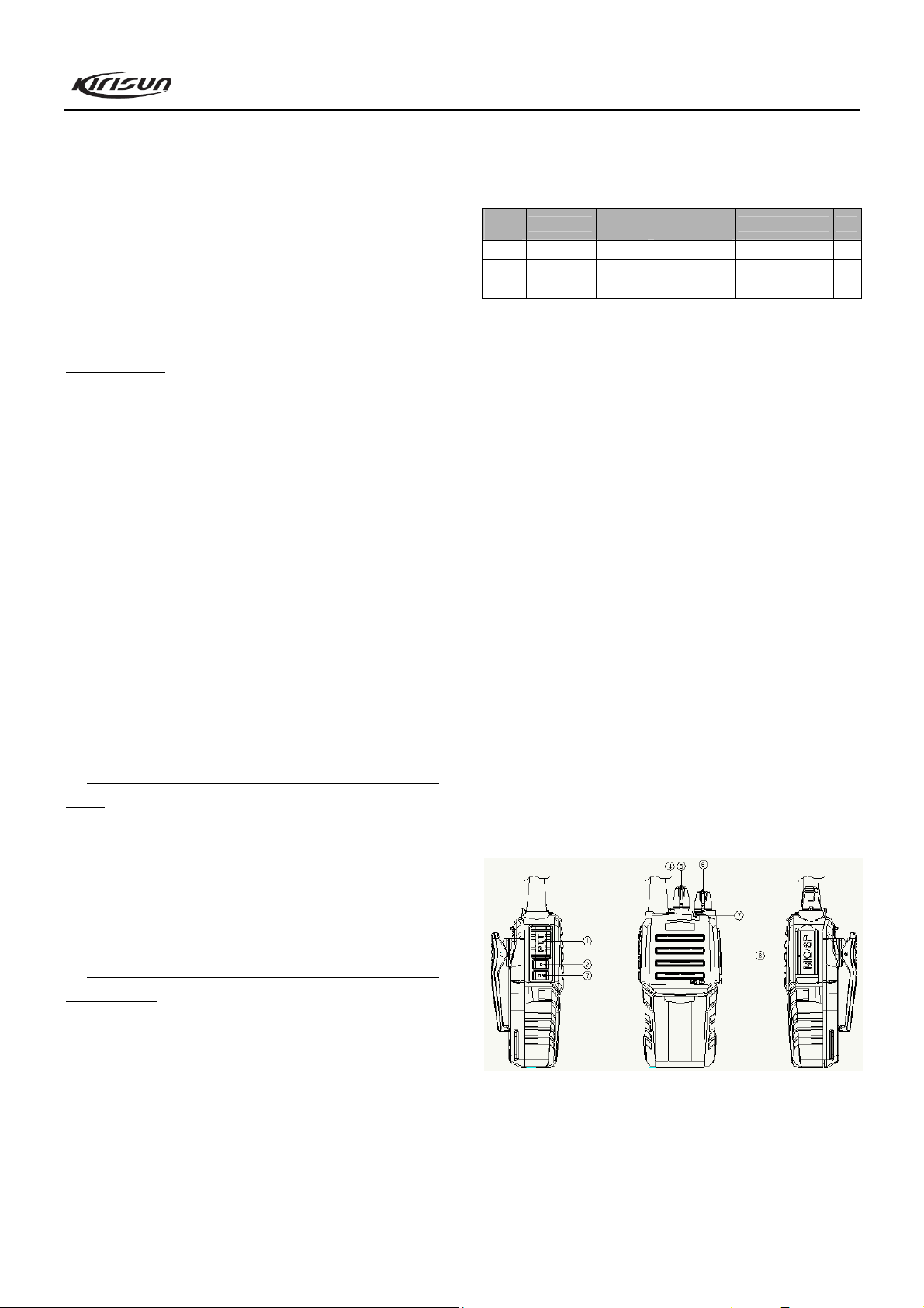
Chapter 2 External View and Functional Keys
2.1 External View
2.2 Functional Keys
① PTT (Push-To-Talk) Button
Press and hold the PTT button and speak into the microphone,
your voice can be sent to the recipient. Release the PTT button to
receive.
2
Page 4
PT3600 Service Manual
② Programmable Button 1
Functions can be assigned to this button through PC software.
③ Programmable button 2
Functions can be assigned to this button through PC software.
④ Emergency Button
Press the button to activate warning tone. Press it again to exit
the emergency alert state. Under the emergency state, all the other
switches and buttons are disabled.
⑤ Channel Selector Knob
Rotate the knob to select channel 1-16.
⑥ On-Off/Volume Control Knob
Turn clockwise until you hear a click to turn the radio power
on. Turn counterclockwise until you hear a click to turn it off.
Rotate it to adjust the volume after turning on the radio.
⑦ LED Indicator
Lights red while transmitting; lights green while receiving;
flashes red when the radio is in low power.
⑧ External Speaker/Microphone Jack Cover
Open the cover; you will see the external speaker/microphone
jacks. External speaker/microphone can be connected to the radio
through these jacks.
Chapter 3 Circuit Description
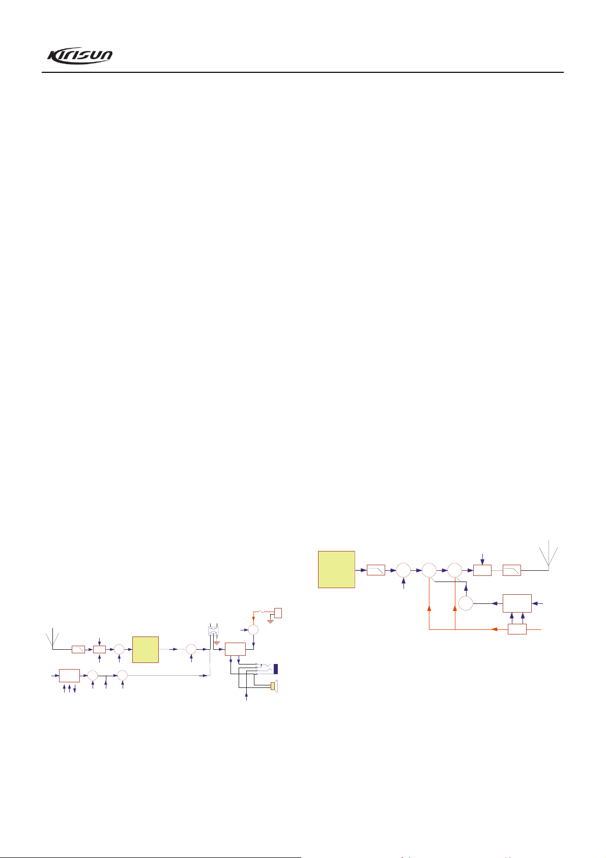
3.1 Frequency Configuration
The receiver adopts single mixing mode. The first IF is
9.375kHz. The first local oscillator signal of the receiver and the
transmitter signal are generated by the frequency synthesizer.
The reference frequency of the frequency synthesizer is
produced by TCXO.
3.2 Receiver (RX)
3A
BAT T
1
23
POWER
AFCN
5T
RF
RDA1846ANT SW
AMP
FROM TX
5R
AF
W558
5M
MUTE
CLK F RO M MC U
DAT A F RO M M CU
BUS Y T O MCU
AF
AMP
MUT E
DTMF/BEEP FROM MCU
5C
MUTE
SW
4
5
GND
AF
MUTE
AF POW ER AMP
Figure 3.1 Receiver Diagram
Front end
The signal coming from the antenna passes through the
RX/TX switch circuit (D511, D515, D508, and D517), and is sent
to pin 15 of U8 (RDA1846) to be demodulated and to output
GND
AF
POWER
sw
SP K JACK
2
2
2
4
4
3
3
1
1
TXD
audio signal.
Audio signal processing
The demodulated audio signal output from U8 (RDA1846)
passes through the volume potentiometer to be adjusted, and then
goes to the audio power amplifier U1 (TDA2822).
Squelch circuit
Output from pin 26 of U8 (RDA1846) is sent to the MCU.
MCU identifies the level of the noise and controls the squelch.
Audio power amplifier
The BTL type audio power amplifier circuit consists of U1
and its peripheral components.
Base electrode of Q621 is the control terminal. High level:
Open; Low level: Close.
The Rx audio signal, voice alert signal, alert tone signal and
warning tone signal are collected and passed through the audio
power amplifier where they are amplified and output to drive the
speaker. The volume of the warning tone is not controlled by the
preset volume level of the radio. Speaker impedance: 16.
Note: Any terminal of the speaker should not be grounded!
CTCSS/DCS signal processing
CTCSS/DCS signal output from pin 32 of U8 (RDA1846) is
sent to MCU for decoding.
3.3 Transmitter (TX)
TX power amplification
5T
PRE
RDA1 846
DRIVER
5T
RF PA
DRI VER
POWER SUPPLY
RF PA
ANT SW
APC
SW
APC
CONTROL
CURRENT
SENSING
Figure 3.2 Power Amplifier and Antenna Switch Diagram
The modulated RF signal from IC4 (RDA1846) is amplified
by Q506, Q507 and Q502, and is sent to Q501 for power
amplification. Output power of Q501: 4.5W.
Grid bias of Q502 and Q501 is controlled by the APC circuit.
Through changing the grid bias voltage, the Tx output power can
be controlled conveniently.
APC (Automatic Power Control)
3
APC FR OM MCU
Page 5
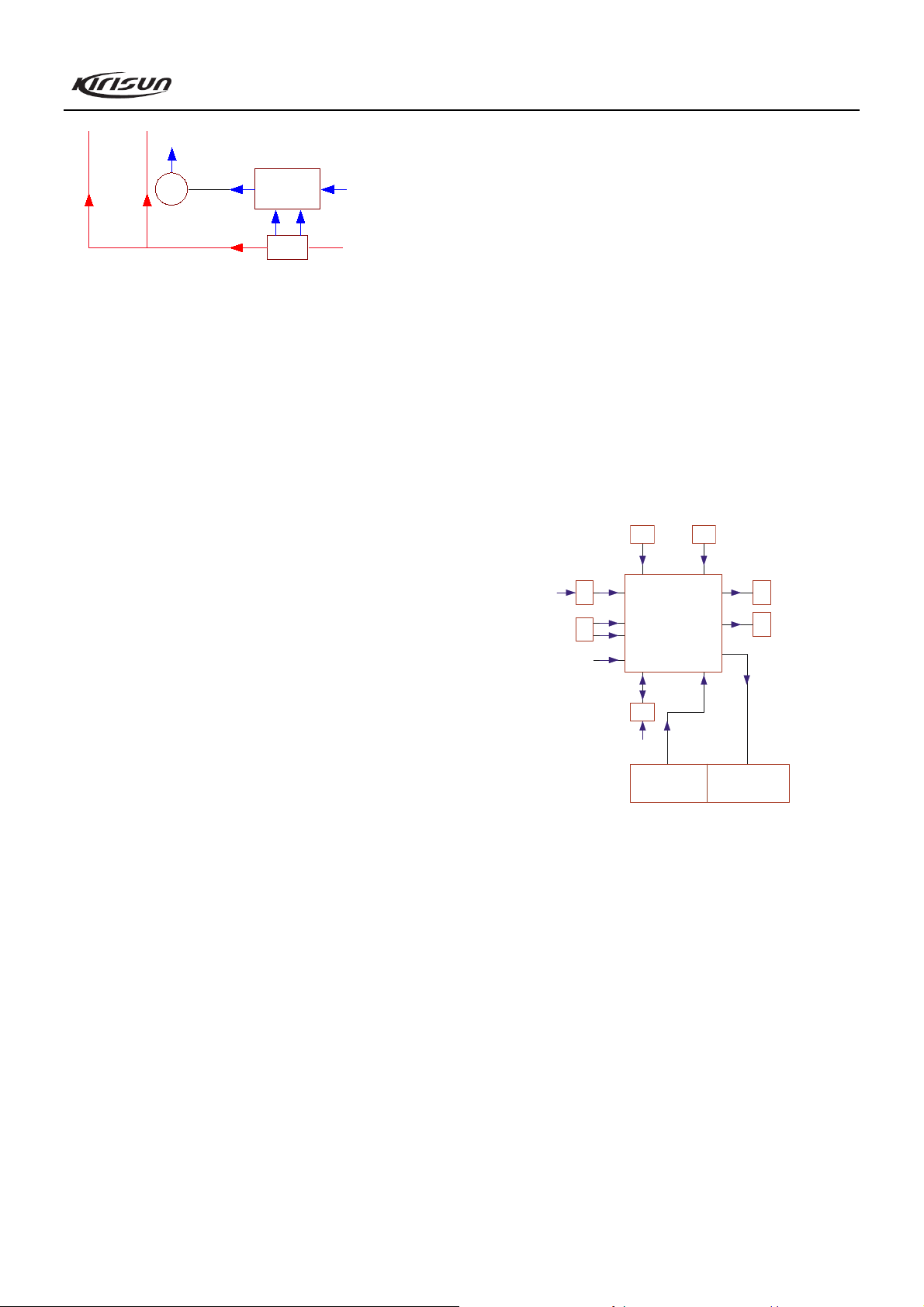
PT3600 Service Manual
APC
SW
POWER SUPPLY
Figure 3.3 APC Circuit Diagram
R525, R523 and R524 are used to test the power amplification
current. IC502A is the sampling amplifier for the power
amplification current. IC502B is the power comparator amplifier.
If the Tx output power is too high, the power amplification
current and IC502A output will increase; IC502B output voltage
will decrease, so the offset voltage added to Q501 and Q502 will
also decrease, which causes the Tx output power to be lowered,
and vice versa. Thus the Tx output power can keep stable under
different working conditions.
MCU can set the power through changing the voltage input to
IC502B.
Tx voice signal processing
MIC signal passes through the internal/external MIC switch
circuit and is sent to pin 11 of U8 (RDA1846) for carrier
modulation.
3.4 Frequency Synthesizer
The 12.8MHz reference frequency signal provided by X603 is
divided by the internal reference frequency divider of U8
(RDA1846), and is then sent to the internal phase comparator of
U8, where the signal is compared with the signal divided by the
fractional frequency divider of internal VCO. Then the output
signal is used to control the internal VCO, enabling the frequency
to reach the set value.
3.5 Voice Alert Circuit
The radio is provided with voice alert function, which is
especially useful at night or in dark environment.
IC305 is a Flash voice memory chip, which is stored with
voices of channel indication etc. Once the channel selector knob is
switched, the speaker will announce the current channel number.
You can press the preprogrammed “Channel Annunciation” button
to repeat the current channel number.
If Channel Annunciation function is enabled, the speaker will
annunciate the current channel number once the “Channel
Annunciation” button is pressed under standby mode. You can
switch the voice type by pressing and holding the “Channel
APC
CONTROL
CURRENT
SENSING
APC F ROM MCU
Annunciation” button while restarting the radio. Do it repeatedly
to switch the voice type in the order of “Chinese Male-English
Male-Chinese Female-English Female-No Alert”.
3.6 Power Supply
The radio uses 7.4V, 1300mAh Li-Poly battery. The Tx power
amplification circuit (Q501 and Q502) and the Rx audio power
amplifier (U1) directly adopt the battery for power supply. Power
of other circuits is supplied by 3.3V regulated voltage.
Q636, Q639: 3V low dropout, micro-power regulators, which
supply 3V power with large current for the radio together with
Q637.
Q637: 3T switch, which is controlled by MCU.
3T: Supplies power for front end of Tx.
U8: 3C power supply, and supplies power for RD1846.
3.7 MCU Unit
ENCODER KEYS
CLK LE 3 RC
MUTE
WDATA
G/R LED RD A1 84 6
WSCLK
TXD
3TC
CFA
3M
MCU
7.3MHz RE S E T
3M
R8C/2 A/2C
EEPROM
3M
KEYAD MODE PTT SHIFT QTOUT PABC
RXD
QTIN
BATT
SQL
DTAT
AFCO AP C
W558C
Figure 3.4 MCU Unit Diagram
MCU unit controls the operation of each unit of the radio so
that all functions can be realized.
Communicate with external PC.
Access the status data of the radio.
Control the transmission and reception of RDA1846.
Obtain status parameters of current channel.
Control status of LED indicator.
Control power supply for each unit.
Check the actions of each functional key.
Generate CTCSS signal.
Generate DCS signal.
Generate power control signal.
Perform CTCSS decoding.
Perform DCS decoding.
Test and control the squelch.
Control content of voice alert.
4
Page 6
PT3600 Service Manual
2
Memory (E
The memory is stored with channel data, CTCSS/DCS data,
other function setting data, and parameter adjusting data.
CTCSS/DCS signal encoding and decoding:
The CTCSS/DCS signal (output from pin 17, PWM wave)
generated by MCU is filtered by R359, R356, C324 and C325.
Then the resulting signal is sent to RDA1846 for modulation.
The CTCSS/DCS signal from the receiver is sent to MCU for
decoding. MCU checks if the CTCSS/DCS signal in the received
signal matches the preset value of the radio, and determines
whether to open the speaker or not.
Power adjustment:
Output signal from pin 19 of the MCU passes through low
pass filter to be changed into DC signal, and is sent to the APC
unit to control the output power of the transmitter.
CTCSS
CTCSS (Continuous Tone Control Squelch System) is a
squelch control system which is modulated on carrier and is
guided by a continuous sub-audio signal. If CTCSS is set, the
communication between the transmitting and receiving radios can
be realized only when the two radios have set the same CTCSS
frequency. In doing this, disturbance from other signals can be
avoided.
PT3600 has 39 groups of standard CTCSS frequencies for
your selection (meanwhile, any CTCSS frequency between 67 and
254.1Hz is compatible). See table 3.1.
The CTCSS signal (PWM wave) is generated by MCU, and is
passed through low pass filter consists of RC to remove high
frequency components (above 300Hz). Then the resulting signal is
sent to VCO for modulation.
No.
1 67.0 11 94.8 21 131.8 31 186.2
2 69.3 12 97.4 22 136.5 32 192.8
3 71.9 13 100.0 23 141.3 33 203.5
4 74.4 14 103.5 24 146.2 34 210.7
5 77.0 15 107.2 25 151.4 35 218.1
6 79.7 16 110.9 26 156.7 36 225.7
7 82.5 17 114.8 27 162.2 37 233.6
8 85.4 18 118.8 28 167.9 38 241.8
9 88.5 19 123.0 29 173.8 39 250.3
10 91.5 20 127.3 30 179.9
PROM, A T24C08):
Frequency
[Hz]
No.
Table 3.1 CTCSS Frequencies
Frequency
[Hz]
No.
Frequency
[Hz]
No.
Frequency
[Hz]
DCS
DCS (Digital Code Squelch), which is used to control squelch,
is a series of continuous digital codes modulated on carrier
together with voice signal. If DCS is set, the speaker can be
opened only when the radio receives signal with the same DCS to
avoid disturbance of unwanted signals.
PT3600 has 83 standard codes (normal and inverse) for your
selection. See table 3.2.
DCS signal (PWM wave) is produced by MCU. It passes
through the low pass filter consists of RC to remove the high
frequency components (above 300Hz). Then the resulting signal is
sent to VCO and TCXO for modulation, with HF components of
the DCS signal being modulated by VCO, and the LF components
of the DCS signal being modulated by TCXO.
The DCS signal coming from the receiver is sent to MCU for
decoding. MCU checks if the DCS code in the received signal
matches the preset DCS of the radio, and determines whether to
open the speaker or not.
Table 3.2 DCS Codes
023 114 174 315 445 631
025 115 205 331 464 632
026 116 223 343 465 654
031 125 226 346 466 662
032 131 243 351 503 664
043 132 244 364 506 703
047 134 245 365 516 712
051 143 251 371 532 723
054 152 261 411 546 731
065 155 263 412 565 732
071 156 265 413 606 734
072 162 271 423 612 743
073 165 306 431 624 754
074 172 311 432 627
3.8 Semiconductor Data
MCU Description
Table 3.3 Microprocessor (R8C/2A/2B) Port Description
Pin No. I/O Port Name Function
1 I/O ERDATA EEPROM data line
2 O EPCLK EEPROM clock line
3 MODE
4 I TOP KEY Top key
5 I UP KEY Up key
6 RESET Reset pin, programming test point
7 I XOUT Oscillator 7.3m
8 VSS/AVSS GND
9 I XIN Oscillator 7.3m
10 I VCC Power supply, programming test point
Connect the 4.7K resistor with VCC,
programming test point
5
Page 7
PT3600 Service Manual
Pin No. I/O Port Name Function
11 I DOWN KEY Down key
12 I PTT KEY PTT key, programming test point
13 O 3TC Tx power control
I/TRCI
14
OA
15 I SQL RDA1846 SQL test input (RDA GPIO6)
16 O RDA PDN RDA1846 power supply control
17 I VOXIN RDA1846 VOX test input (RDA GPIO7)
I/TRDI
18
OB1
19 O SHIFT Beat shift selection
O/TRD
20
IOD0
O/TRD
21
IOC0
O/TRD
22
IOB0
23 I RDA GPIO4 Connect to RDA1846 GPIO4
24 I/INT1 RDA INT
25 O MAXAF Max. audio frequency
26 I RDA GPIO5 Connect to RDA1846 GPIO5
27 O AFCO Audio frequency amplifier power supply
28 O 3RC Rx power supply control
29 O UVSEL UHF and VHF switch control
30 I RDAOSC RDA crystal frequency selection
31 O RDA EN RDA1846 enabling control
32 O RDA CLK RDA1845 clock line
33 I/O RDA DATA RDA1845 data line
34 O - -
35 O - -
36 O - -
O/TXD
37
I/RXD
38
39 O - -
40 O - -
41 O - -
42 O - -
43 O - -
44 O - -
45 O - 46 O FlashClk Flash IC clock(for FLASH IC and W588)
47 I/O FlashDio Flash IC data input/output
48 O FlashCs Flash IC selection
49 O FlashDo Flash IC data output
50 I ENC0 Encoder input
51 I ENC1 Encoder input
52 I ENC2 Encoder input
53 I ENC3 Encoder input
54 O GLED Green LED control
55 O RLED Red LED control
56 O SPKC Speaker second level control switch
57 I/AN2 LOW BATT Low battery test input
58 O/DA0 BEEP
59 I VSS/AVSS MCU(GND)
60 - - -
61 I VREF A/D reference voltage
62 I VCC MCU power supply
63 - - -
64 - - -
CTCSS/CDCSS
CTCSS/CDCSS
1
1
2T/5T IN
INPUT
OUTPUT
CFA Frequency stability output (TimerD PWM)
APC
TXD RS-232C output (programming test point)
RXD RS-232C input (programming test point)
TONE test input (reserved), programming
test point, connect to RDA1846 GPIO1
CTCSS/CDCSS input (TimerD input
capture),(RDA GPIO0)
CTCSS/CDCSS output(TimerD PWM )
(RDA GPIO0)
Automatic power control output (TimerD
PWM)
RDA1846 interrupt signal detect ( RDA
GPIO2)
Alert tone/TONE output(and connect to
RDA GPIO1)
Chapter 4 Function Description and
Parameter Setting
4.1 Main Functions
4.1.1 Programmable Buttons
Long Press Duration: Amount of time that the radio-user is
required to press (and hold down) a button, for the press to be
interpreted by the radio as a long press. A short press is defined as
any button-press that is shorter than the duration.
The dealer can assign one of the following auxiliary functions
to the long press or short press of the programmable button 1 and
programmable button 2:
● None: No function is assigned.
● Monitor Momentary
Press and hold the preprogrammed Monitor Momentary button
to open squelch for monitoring the transmission on the channel
whether the CTCSS/DCS, audio squelch conditions match or not.
Release it to exit monitor mode. Press this button can also cancel
the current incoming call.
● Monitor
Press the preprogrammed Monitor button to open squelch for
monitoring the transmission on the channel whether the
CTCSS/DCS, audio squelch conditions match or not or cancel the
current incoming call. Press it again to exit monitor mode.
● Squelch Off Momentary
Press and hold the preprogrammed Squelch Off Momentary
button to open squelch momentarily, and release it to resume
normal operation. Press this button can also cancel the current
incoming call.
● Squelch Off
Press the preprogrammed Squelch Off button to open squelch,
and press it again to resume normal operation. Press this button
can also cancel the current incoming call.
● Channel Annunciation
Press the preprogrammed Channel Annunciation button, the
current channel number can be heard.
● Scan
Press the preprogrammed Scan button to start scanning (the
scan list should be effective), press it again during the scanning to
stop scanning.
● High/Low Power Switch
Press the preprogrammed High/Low Power Switch button to
switch the current channel power between high and low.
● Battery Check
Press the preprogrammed Battery Check button, the current
battery power level can be heard. There are four levels in all.
6
Page 8

PT3600 Service Manual
Level 4 indicates that the battery power is full, and level 1
indicates that the battery power is low.
● Squelch Adjust
Press the preprogrammed Squelch Adjust button to change the
current squelch level, and the squelch level after the change can be
heard.
4.1.2 VOX
VOX function enables you to use the radio without manual
operations. This function can only be set by the dealer, and you
have to be equipped with the specified earphones.
Before using VOX, you must set VOX gain level. Such setting
enables the radio to identify the voice volume. If the microphone
is too sensitive, the background noise will trigger the radio to
transmit. If the microphone is not sensitive enough, it cannot
receive your voice when you speak. Make sure to adjust the VOX
gain level to proper sensitivity.
4.1.3 Scan Function (this function can be disabled by the dealer)
If the scan function is enabled, you can press the
preprogrammed Scan button to start scanning and press it again to
stop scanning.
Explanations:
● After scan pauses, there are two ways to resume scanning:
1. Time operate: After pausing on an active channel, the radio will
resume scanning after a preprogrammed delay. The scan delay
time can be preset from 0.5 to 5 seconds.
2. Carrier operate: After pausing on an active channel, the radio
will resume scanning after a preprogrammed delay after the
channel becomes inactive. The scan delay time can be preset from
0.5 to 5 seconds.
● The revert channel during scan can be designated through PC
software. There are following options available:
1. Last Rx channel:
When pressing the PTT button during scanning, the radio will
transmit from the last channel that received a call.
2. Designated Tx channel:
When pressing the PTT button during scanning, the radio will
transmit from the designated TX Ch.
3. Priority channel (the priority channel must be set)
When pressing the PTT button during scanning, the radio will
transmit from the priority channel in the scan list.
4. Last Tx channel:
When pressing the PTT button during scanning, the radio will
transmit from the last channel that transmits signals.
5. Selected channel:
When pressing the PTT button during scanning, the radio will
transmit from the channel selected by the channel selector knob.
● You can choose to set one of the following 3 operations when
the channel is switched during scanning:
1. No operation.
2. Scan the current channel: The scanning will pause on the
current channel, and the pause time will be the Dropout Delay
Time. However, this channel will not be added to the scan list.
3. Exit scanning.
● Power-on scanning: If this function is enabled, the radio will
start scanning after the radio power is turned on.
4.1.4 CTCSS/DCS
CTCSS (Continuous Tone Control Squelch System) and DCS
(Digital Code Squelch) are sub-audible signals, which can realize
selective call and group call function. Only radios with the same
CTCSS/DCS can realize communication. CTCSS/DCS are preset
on channels of the radio.
4.1.5 TOT (Time-Out Timer) Function
The time-out-timer can prevent the user from continuously
talking and occupying a channel overlong, which will influence
the team communication.
If you continuously transmit longer than the preset TOT time,
the radio will make an alert tone and stop transmitting. To stop the
warning tone, release the PTT button.
4.1.6 TOT Pre-alert
The TOT Pre-Alert is the number of seconds the alert tone will
sound before the Time Out Timer times out. If the continuous
transmit time exceeds the preset limit, the radio will make alert
tone, which signifies that the communication is going to be
overtime.
4.1.7 TOT Rekey Time
A period in which the radio is forbidden to transmit after its
overtime activity. During the period, if the PTT button is pressed,
an alert tone will be sounded, and the transmission is forbidden.
4.1.8 TOT Reset Time
The time delay from releasing the PTT button to the resetting
of the timer is limited. The countdown will go on if the time after
releasing the PTT key is shorter than the reset time.
7
Page 9
PT3600 Service Manual
4.1.9 Automatic Battery Saving
If no signal is received and no operation is conducted for over
8 seconds, the radio will enter Battery Saving Mode. When a
signal is received or any operation occurs, the radio will exit the
Battery Saving Mode automatically. The battery save proportion
can be set to Long or Short. Long proportion has longer standby
time.
4.1.10 Low Battery Warning
When the battery voltage drops too low, the indicator will
flash. If the battery voltage drops too low while transmitting, the
indicator will flash red. When the radio make alert tone of “Di,
Di…”, the radio is prohibited to transmit.
4.1.11 Monitor
When there is no signal received, the radio's squelch circuit
will mute the speaker automatically so that the background noise
will not be heard by the user.
You can press and hold the preprogrammed Monitor button to
open squelch manually. Then the speaker will make sound
continuously (whether signals are received or not). This function
is especially useful when you need to adjust the volume level or to
receive weak signals (avoid weak signals intermitting).
When the Monitor button is pressed and held, the LED
indicator lights green, and the radio is in the monitoring state.
4.1.12 Busy Channel Lockout (BCL)
If BCL function is enabled, transmission is prohibited when
the channel is busy. If you press the PTT button on a busy channel,
an alert tone of “Di, Di, Di” will be sounded, and the transmission
will be prohibited.
4.1.13 PC Programming
You can set the functions of the radio and adjust part of its
parameters through PC programming software KSP3600.
4.1.14 Wired Clone Mode
Parameters of a radio can be transferred to other radios of the
same model by using a special clone cable.
4.1.15 Squelch Level
Squelch function is used to mute the speaker when there is no
signal or only weak signals are received. The speaker will unmute
when the squelch is opened, and will mute when the squelch is
closed. The function of selecting a squelch level is to determine
the signal strength for open and close squelch. If the signal
strength is stronger than the set level, the squelch will be opened,
and if the signal strength is weaker than the set level, the squelch
will be closed. If the squelch level is set too high, weak signals
will not be received effectively; if the squelch level is set too low,
you will be interfered by noise or other irrelevant signals. Squelch
level can be set to 0 – 9.
4.2 Functional Parameter Setting (PC Mode)
The radio has been set before leaving the factory. However,
due to different requirements of users, the radio’s operating
frequency, channels, CTCSS/DCS, scan, and other functional
parameters should be reprogrammed. Therefore, Kirisun has
specially designed a set of Chinese/English programming software
KSP3600 with friendly interface, convenient operation and
visualized display for setting functional parameters of the radio.
Steps for setting the functional parameters of the radio by PC
are as follows:
A. Install KSP3600 on the PC.
B. Connect the radio to the serial port of the PC with the special
programming cable (KSPL02). Refer to the figure below.
Computer
(RS232 serial port)
Programming
cable (KSPL02)
Radio
(Speaker/MIC Jack)
Figure 4.1
C. Turn the computer power ON.
D. Turn the radio power ON.
E. Run the KSP3600 programming software by double clicking on
its execution program.
F. Click “Read” in the main menu of KSP3600 to read parameters
of the radio to the computer; click “Write” to write parameters in
the computer to the radio.
G. The following parameters can be set by using KSP3600
according to requirements of the user:
1) Receive and transmit frequency for each channel;
2) CTCSS/DCS encode and decode for each channel;
3) Busy Channel Lockout selection;
4) TOT
5) Squelch level selection;
6) Battery saving selection
7) Monitor mode selection
8) Scan mode selection
9) Scan revert channel selection
10) Scan priority channel selection
Please refer to the “Help” document of KSP3600 for details.
Note:
1. Turn the radio power off before connecting it to the computer.
2. When reading data from the radio, the radio’s LED indicator
8
Page 10
PT3600 Service Manual
will flash red. Do not press the PTT button at this moment. When
writing data to the radio, the radio’s LED indicator will flash
green.
3. Please firstly read data of the radio and back up the data before
editing the parameters on KSP3600.
4. If the radio cannot function normally after being written in with
the edited data, please rewrite the backup data into the radio.
5. “Model Information” is important for the radio; users should
not modify it.
4.3 PC Test Mode
Connect the radio to the serial port of the computer with the
special programming cable. Refer to figure 4.1.
Warning: Before entering the PC Test Mode, please firstly
connect a 50 HF load to the antenna connector of the radio or
connect the radio to a general test set.
With the KSP3600 programming software, you can enter the
Test Mode to adjust the following parameters of the radio:
1) Middle frequency
2) Tx power
3) Battery
4.4 Wired Clone Mode
Wired clone function can be used to improve the working
efficiency. After setting parameters of a radio, you can copy the
data of the radio (master) to another radio (slave) using a special
clone cable.
The operation procedure is as follows:
a. Turn the master radio power off. Press and hold the Monitor
button while turning the radio power ON until the red LED flashes
twice and two beep tones sound to enter the Wired Clone Mode.
b. Connect the slave radio to the master radio by the special
clone cable, see figure 4.2.
Clone Cable
Master Radio Slave Radio
Figure 4.2
c. Press the Monitor button of the master radio to start cloning.
The LED on the master radio will light red when data of the
master is sent to the slave.
d. While the slave is receiving the data, the LED lights green.
Note: The data being cloned includes all the data in “4.2
Functional Parameter Setting” but the adjustment parameters in
“4.3 PC Test Mode”.
Chapter 5 Disassembly for Repair
The radio is a piece of precision communication equipment.
Please be careful when disassemble the radio during service. The
instructions for the disassembly are as follows.
5.1 Attaching and Removing the Battery
1) Attaching the Battery
Match the two bulges at the bottom of the battery pack with
the corresponding slots at the rear bottom of the radio. Press the
top part of the battery towards the radio to lock it in place until a
click is heard.
2) Removing the battery
To remove the battery pack, push the battery latch upwards,
and then remove the battery away from the radio.
Note:
* Do not short-circuit the battery terminals or dispose battery
in fire.
* Do not disassemble the battery casing by yourself.
5.2 Installing the Antenna
Hold the base of the antenna and turn the antenna clockwise
into the connector on the top of the radio until secure.
5.3 Installing the External Speaker/MIC
Open the cover for external speaker/MIC jacks, and then insert
the external speaker/MIC plug into the jacks on the radio.
Note: When using the external speaker/MIC, the radio will not
be waterproof.
5.4 Installing and Removing the Belt Clip
Align the grooves of the belt clip with those on the rear of the
battery. Then press the belt clip downwards until a click is heard.
9
Page 11

PT3600 Service Manual
To remove the belt clip, use your fingernail or a tool to press
the belt clip tab away from the battery. Then slide the belt clip
upwards to remove it.
5.5 Removing the chassis from the front casing
1. Pull out the volume knob and the channel selector knob;
2. Remove the two nuts for knobs and the nut for the antenna
connector;
3. Remove the two torx head fixing screws for the top cover;
4. Remove the two torx head fixing screws at the lower part of the
Al alloy chassis;
5. Insert a flat-blade screwdriver into the slot at the bottom of the
Al alloy chassis, and prize it up.
6. Pull the Al alloy chassis backwards to remove it from the front
casing.
5.6 Removing the mainboard from the Al alloy chassis
1. Remove the screws on the PCB;
2. Remove the main waterproof for the Al alloy chassis;
3. Remove the solder of the antenna connector with a soldering
iron, and remove the mainboard;
4. Remove the two screws fixing the antenna connector, and
remove the connector.
5.7 Exploded View
10
Page 12

PT3600 Service Manual
No. Part No. Description PCS Remark
1 7MHR-7123-01A-W9 Light guide 1 Silica gel, transparent, ROHS
2 7PLJ-7123-E01A LOGO 1
3 7MHP-7123-05A-W0 Cover for external speaker/MIC jacks 1 TPU, black, ROHS
4 7MHP-7123-01A-W0 Front casing 1 PC+ABS, black, ROHS
5 7GCB-360001-W0 Protective net for speaker 1
6 7GCB-070005 Dustproof net for MIC 1
7 7SMF-020040M-SZYB-N1 M2.0*4.0 pan plus machine screws 8 For fixing the PCB
8 7MHR-1727-09A-W3 MIC waterproof 1 Silica gel, hardness 40, orange, no surface treatment
9 6PM7-7115-HMA PT3600 mainboard 1
10 7MHR-7042-05A-W0 PT568 waterproof gasket for bracket 1 Silica gel, black, hardness 60, ROHS
11 7MHP-7042-11A-W PT568 battery connector assembly 1
12 7MHP-7123-07A-W0 MIC/SPK jack cover plug 1 PC+ABS, black, ROHS
13 7SMF-020080M-MHHT-N1 M2*8 Torx thick head machine screws 2 For fixing Al alloy chassis
14 7MDP-7126-02A-W0 Battery bottom casing 1 PC+ABS, black, ROHS (with hardware piece)
15 6BPM-063760-074130-A KB-31A Li-poly battery pack 1 M063760Q01,TCL,7.4V,1300mAh, ROHS
16 7MDP-7126-01A-W0 Battery top casing 1 PC+ABS, black, ROHS (with hardware piece)
7MJP-1740-02A-W0
17
(7ML-1826-01A-L0,
7MJS-1826-01A-W)
18 7MJS-7128-01A-N KBJ-10 Belt clip bolt 1 Carbon steel, Ni-plated, ROHS
19 7MJP-7128-01A-W0 Belt clip 1 PC+ABS, black, ROHS
20 7MJS-3851-02A-W KBJ-01 Spring 1 Stainless steel, ROHS
21 7SMF-025050M-MHYB-Z2
22 7MHP-7123-08A-W0 Battery latch 1 PC+ABS, black, ROHS
23 7MHS-1727-02A-N Battery latch spring 1 Carbon Spring Wire 0.35,∮ Ni-plated, ROHS
24 7MHP-7123-06A-W0 Top cover 1 PC+ABS, black, ROHS
25 7MHR-7123-02A-W0 Main waterproof 1 Black silica gel, hardness 45, ROHS
26 7MHL-7123-01A-WA Al alloy chassis 1 ADC12, abrasive, polished, ROHS
27 3CR7-SMA-50JFB-4 PT558 antenna connector 1 Ni-plated brass, ROHS
28 7SMF-020040M-SZYB-N1 M2.0*4.0 Pan plus machine screws 2 For fixing the antenna connector
29 7NRC-060100035-B1 Switch nut 2
30 7NRC-090136039-B1 Antenna nut 1
31 3SE3-RE08140AX-V01 Encoder switch 1
32 2RW3-R08710NS-A103 Volume potentiometer 1
33 7MHP-1010-15A-W 3208 PVC MIC gasket 1 Transparent PVC, 0.5mm thick
34 4SS7-4005-016-100B 7200 speaker 1
35 7MHP-7123-04A-W0 PTT button cover 1 PC+ABS, black, ROHS
36 7MHR-7123-03A-W0 PTT button 1 Black silica gel, hardness 60, ROHS
37 xxxxxxxxx PT3600 antenna 1
38 7MHP-7123-03A-W3 Channel selector knob 1 ABS, black, painted, ROHS
39 7MHP-7123-02A-W0 Volume knob 1 ABS, black, painted, ROHS
40 7MHR-7123-04A-W3 Emergency button 1 Orange silica gel, hardness 60, ROHS
KBJ-05 Belt clip bracket (metal bracket) 1 PC+ABS, black, ROHS (Al alloy, stainless steel)
M2.5*5 Pan torx black Zn-plated
machine screws
Black waterproof cloth, diameter 36mm* thick
0.1mm
Black non-woven cloth, diameter 7mm* thick
0.5mm, waterproof
2 For fixing the top cover
Brass, inner diameter M6mm, outer diameter
10mm, thick 3.5mm, black passivation
Brass, inner diameter M9mm, outer diameter
13.6mm, thick 3.9mm,
40*H4.8, impedance 16, power 1W, gold-plated
11
Page 13

PT3600 Service Manual
Chapter 6 Adjustment
Before test/adjustment, make sure all equipment has been well
connected to the ground!
Before test/adjustment, make sure the antenna output terminal
has been correctly connected to corresponding equipment or load!
The transmitter output terminal must be terminated with an RF
power attenuator and connected to a standard signal generator
(SSG)/frequency counter/deviation meter/spectrum analyzer!
Make sure no transmission operation is being conducted while
measuring the receiver!
During the adjustment/test/maintenance, make sure reliable
anti-static measures are taken for human body and equipment.
6.1 Equipment and Software Required for Service
Equipment and software listed in Table 6.1 are required for
test and service of PT3600.
Table 6.1 Equipment and Software Required for Test and Service
No. Item Specifications
1 Computer
Programming
2
software
Programming
3
cable
4 Clone cable KCL-01
DC regulated
5
power supply
6 RF power meter
7 Frequency counter
8 Deviation meter
9 DMM
Audio signal
10
generator
RF power
11
attenuator
Standard signal
12
generator
13 Oscilloscope
Audio frequency
14
voltmeter
Recommendation: Item 6, 7, 8, 10, 11, and 12 listed in the
table can be replaced by HP8920 general test set.
Item Test condition Test equipment
P2 or above, IBM compatible PC, WINDOWS
98/ME/2000/XP Operating System
KSP3600
KSPL-02
Output voltage: 7.5V
Output current: 5A
Measurement range: 0.5-10W
Frequency range: 100MHz-500MHz
Impedance: 50
SWR 1.2
Frequency range: 0.1 - 600MHz
Frequency accuracy: better than ±1×10⁻⁶
Sensitivity: better than 100mV
Frequency range: DC - 600MHz
Measurement range: 0 - ±5kHz
Input impedance: above 10M/V DC, capable of
measuring voltage, current and resistance.
Frequency range:2-3000Hz
Output level: 1-500mV
Attenuation: 40dB or 50dB
Supporting power : higher than 10W
Frequency range: 10MHz-1000MHz
Output level:
0.1uV-32mV (-127dBm~-17dBm)
Frequency range: DC~20MHz
Measurement range: 10mV-20V
Measurement range: 10mV-10V
Table 6.2 Transmitter Section
6.2 Adjustment Items
During the course of maintenance, it is necessary to test the
radio and adjust its technical parameters after changing
components. The following part is going to introduce the
adjustment items.
Some parameters can be adjusted by use of KSP3600
programming software (in the Test Mode). The adjustable
parameters are as follows:
1) Middle frequency
2) Tx power
3) Battery
Steps for adjustment:
a. Enter PC Test Mode. Refer to Section 4.3.
b. Click “Tools” in the main menu of KSP3600 programming
software, and then click “Test Mode” in the pull-down menu to
enter.
c. Then the test screen will pop up. Double click the item you
want to adjust, and then you can adjust the parameters.
d. Exit the PC Test Mode after adjustment.
6.3 Adjustment
6.3.1 PLL frequency
In the Test Mode, double click “Middle Frequency” to enter.
Adjust the parameter among 0-255 to make the Tx frequency at
the rated value (error within 200Hz).
6.3.2 Tx power
In the Test Mode, double click “High Power (Low)” to enter.
Adjust the parameter among 0-255 to make the Tx power at 4W.
Meanwhile, observe the operating current, and make sure that the
current 1.8A.
Use this method to adjust “High Power (Lower)”, “High
Power (Mid)”, “High power (Higher)”, “High Power (High)”, and
make the Tx power at 4W.
6.3.3 Tx low battery voltage warning
Set the voltage of the power supply at 6.8V.
In the Test Mode, double click “Battery” to enter. Adjust the
parameter among 0-255 to make the red LED flash.
6.4 Adjustment Description
See Table 6.2.
Measuring
terminal
Adjustment
parts
Requirement Remark
12
Page 14

PT3600 Service Manual
Middle
frequency
Power
Low battery
warning
Battery terminal:6.8V
Chapter 7 Specifications
7.1 General Specifications
Product Model PT3600
Frequency 400 ~ 470MHz 136 ~ 174MHz
Modulation Type 16K0F3E
Number of Channels 16 (15 + S)
Channel Spacing 25 kHz (W) / 12.5kHz (N)
Intermediate Frequency None
Operating Voltage 7.5V Negative grounded
Operating Temperature -25℃~ +55℃
Antenna Impedance 50
MIC Impedance 1.8k
Battery (Standard
Configuration)
Dimension (W×H×D) 56mm × 102mm × 29mm
Weight 235g (with battery and antenna)
7.2 Receiver Section
Usable Sensitivity (12dB SINAD) 0.25V
Open Squelch Sensitivity 0.18V@ squelch level 3
Residual Output -45dB
Modulation Receiving Bandwidth ± 7kHz
Adjacent Channel Selectivity 65dB
Intermodulation Rejection 60dB
Spurious Response Rejection 60dB
Audio Output Power Internal speaker: 1W, balance
Receiving Consumption Current 250mA
Standby Current (Average) 20mA
7.3 Transmitter Section
Tx Power 4.5W @7.4V DC
Frequency Stability ±2.5×10⁻⁶
Max. Modulation Deviation ±5kHz
Modulation Sensitivity 12mV
Modulation Distortion (300-3000Hz) 3%
Adjacent Channel Tx power -70dB
Spurious Tx -70 dB
Residual FM -45 dB
Tx Power Consumption Current 1.8A @ 7.5V DC
Model: KB-31A, Li-Poly Battery, DC
7.4V 1300mAh
@ distortion 5%, 16
External speaker: 125mW,
unbalance @ distortion 5%,
16
Frequency
counter/General test set
Power meter/General test
set, Ammeter
Error within
±200Hz
Error within
±0.2W
Indicator flashes
after adjustment
Antenna
PC Test Mode
PC Test Mode Adjust to 4W
PC Test Mode
Chapter 8 Troubleshooting
No. Problem Causes and Solutions
1 No display after
switching on
the radio
2 Cannot talk to
or hear other
group members
3 Cannot receive
signals
4 The
transmitting red
light is on, but
no voice is
heard by the
recipient.
5 The receiving
green light is
on, but no voice
is heard.
6 Cannot program
the radio
parameters
normally
A. Battery power may be insufficient, please recharge
or change the battery pack.
B. The power switch is broken, please change it.
C. The CPU is broken, please change the IC.
D. The regulator tube is broken, please change the IC.
A. The frequencies of both users are not the same,
select the same frequency channel.
B. The CTCSS/DCS of both users are not the same.
Please reset it with PC.
C. The radio is out of the effective communication
range.
A. The antenna is in poor contact. Please fasten the
antenna until secure.
B. The HF amplifier is broken. Please change it.
C. The squelch level is so high that the squelch cannot be
opened. Please reset the squelch level with PC.
A. The power amplifier tube Q11 is broken, so there
is no power output, please change it.
B. The microphone is broken, please change it.
A. The speaker is broken. Please change it.
B. The audio power amplifier is broken. Please
change the IC.
A. The cable connection is wrong, please check the
cable connection.
B. The computer RS232 serial port output is
abnormal, please check the computer.
C. The external MIC/Speaker jack is in poor contact,
please change the jack.
Chapter 9 KBC-31A Charger
9.1 Working Conditions and General Specifications
a) Applicable battery: Li-poly (2*3.7v) and Ni-MH (6*1.2) battery
(battery capacity: 1 – 2.4AH).
b) Applicable power adapter: DC 11V-16V, 500 - 1500mA.
Voltage of standard power adapter: 12V.
c) Idling input current: 15mA.
d) Pre-charge current: 75mA ± 10mA.
13
Page 15

PT3600 Service Manual
e) Pre-charge time limit: 15Min.
f) Constant charging current: 400mA ± 40mA.
g) Max. charging voltage for Li-poly battery: 8.32 – 8.42V;
Max. charging voltage for Ni-MH battery: 9.6 ± 0.1V.
9.2 Function Description
1. KBC-31A is an intelligent charger which is safe and reliable,
and has fast charging speed and high charging saturation.
2. Status indication function: In the pre-charge process, the red
LED will flash; in the charging process, the red LED will light; if
the radio is fully charged, or no battery is inserted into the charger
slot, or the battery is in the protection status, the green LED will
light; if the battery output is in short circuit, the yellow LED will
flash.
3. External port of KBC-31A can identify Li-poly battery and
Ni-MH battery.
4. Short circuit protection: If the positive and negative terminals
of the charger are in short circuit, the yellow LED will flash, and
the charging current will be cut off. After the fault is removed, the
charger will resume normal operation.
5. Fully charged battery identification: If the user recharges a
Ni-MH battery that has been fully charged, the charger will still
charge the battery, and will judge if the battery is fully charged
according to normal –V; if the user recharges a Li-poly battery
that has been fully charged, the charger will detect the voltage of
the battery. If the voltage is higher than 8.25V, the charger will not
charge; if the voltage is lower than 8.25V, the charger will charge
the battery again.
6. Temperature protection: For Li-poly battery, when the
temperature is higher than 55℃, the charger will stop charging,
and the yellow LED will light; when the temperature comes back
to 45℃, the charger will start charging again. For Ni-MH battery,
when the temperature is higher than 60℃, the charger will stop
charging, and the yellow LED will light; when the temperature
comes back to 50℃, the charger will start charging again.
7. When the radio is in the standby mode, if it is inserted into the
charger slot, the charger will charge it automatically if the battery
voltage is lower than 8.2V.
8. If the charger is in the automatic protection state, the yellow
LED will light. After the fault is removed, the charger will resume
normal operation.
Red LED: Charging indication
Green LED: Power indication or charging completion indication
Yellow LED: Abnormal charging indication
Appendix 1 Abbreviations
AMP: Amplify, amplifier
ANT: Antenna
APC: Automatic Power Control
BPF: Band Pass Filter
CTCSS: Continuous Tone Control Squelch System
DCS: Digital Code Squelch
DEMOD: Demodulation
2
E
PROM: Electrical Erasable Programmable Read Only Memory
HPF: High Pass Filter
IDC: Instantaneous Deviation Control
IF: Intermediate Frequency
LED: Light-Emitting Diode
LNA: Low Noise Amplifier
LPF: Low Pass Filter
MCU: Micro Control Unit
MIC: Microphone
MOD: Modulation
MONI: Monitor
PLL: Phase Lock Loop
PTT: Push-to-talk
RX: Receiver
SPK: Speaker
TCXO: Temperature Compensated Crystal Oscillators
TX: Transmitter
UL: Un-lock
VCO: Voltage Control Oscillator
14
Page 16

PT3600 Service Manual
Appendix 2 Electronic Parts List
PT3600-01
No. Part No. Name Specifications Unit Qty Position Mark
1 2RW3-RP08110SNAX-B Volume Switch RP08110SNAX-V01-0037,A103, ROHS PCS 1 SW403
2 3CE3-EJ-2507-CCPAK Plug-in Earphone Socket 2.5,EJ-2507-CCPA PCS 1 J502
3 3CE3-ST212-35K Plug-in MIC Socket 3.5,ST212-3.5 PCS 1 J503
4 3SE3-RE08140AX-V01-A Encoder Switch RE08140AX-V01-0000,16P16, ROHS PCS 1 SW404
5 3ST3-454548 Plug-in Touch Switch 4.5*4.5*4.8 PCS 2 SW305,SW303
6 3ST3-SKHLLBA010 Plug-in Touch Switch SKHLLBA010 imported, 7.5*7.5*4.0 PCS 1 SW302
7 4SM7-6027-A40B Microphone
8 7GCM-050050010-J
9 7GCJ-S1727-A
10 7MHP-1010-15A-W 3208 PVC MIC Gasket Transparent PVC, 0.5mmTHK PCS 1
11 7MHP-1727-10A-JC 558 Potentiometer Gasket
12 5XT1-CSTCR-7R30G53 Chip Ceramic Resonator CSTCR7M30G53-R0 PCS 1 X301
13 5OT1-12R8-CEC3-0503 Chip TCXO
14 5FE1-BLM21P300S Chip EMI Control Filter 2012,BLM21P300S/BLM21PG300S(0149-05) PCS 4 L512,L513,L634,L636
15 5FE1-BLM11A221SPT Chip EMI Control Filter
16 4PE1-16-F5 Chip LED 1608, green, H19-213SYGC PCS 1 LED303
17 4PE1-16-F2 Chip LED 1608, red, 19-21SUR/S530-A2/TR8 PCS 1 LED304
18 3ST1-SKRTLBE010 Chip Touch Switch SKRTLBE010,4.5*3.55*3.3mm(ALPS) PCS 1 SW304
19 2RS1-32-R47J Chip Resistor 3216,0.47±5% PCS 3 R523,R524,R525
20 2RS1-16-473J Chip Resistor 1608,47K±5% PCS 1 R288
21 2RS1-16-224J Chip Resistor 1608,220K±5% PCS 1 R448
22 2RS1-16-221J Chip Resistor 1608,220±5% PCS 1 R511
23 2RS1-16-153J Chip Resistor 1608,15K±5% PCS 1 R532
24 2RS1-16-105J Chip Resistor 1608,1M±5% PCS 1 R537
25 2RS1-16-104J Chip Resistor 1608,100K±5% PCS 1 R445
26 2RS1-16-102J Chip Resistor 1608,1K±5% PCS 1 R447
27 2RS1-16-000O Chip Resistor 1608,0 PCS 4 R449,C579,L639,R444
28 2RS1-10-823J Chip Resistor 1005,82K±5% PCS 1 R509
29 2RS1-10-822J Chip Resistor 1005,8.2K±5% PCS 3 R346,R366,R522
30 2RS1-10-683J Chip Resistor 1005,68K±5% PCS 6 R270,R286,R301,R513,R208,R209
31 2RS1-10-563J Chip Resistor 1005,56K±5% PCS 5 R373,R377,R379,R381,R534
32 2RS1-10-562J Chip Resistor 1005,5.6K±5% PCS 1 R546
33 2RS1-10-474J Chip Resistor 1005,470K±5% PCS 1 R300
34 2RS1-10-473J Chip Resistor 1005,47K±5% PCS 12
35 2RS1-10-472J Chip Resistor 1005,4.7K±5% PCS 7 R323,R353,R356,R359,R362,R651,R655
36 2RS1-10-471J Chip Resistor 1005,470±5% PCS 1 R292
37 2RS1-10-470J Chip Resistor 1005,47±5% PCS 1 R510
38 2RS1-10-393J Chip Resistor 1005,39K±5% PCS 1 R512
39 2RS1-10-392J Chip Resistor 1005,3.9K±5% PCS 2 R283,R303
40 2RS1-10-334J Chip Resistor 1005,330K±5% PCS 2 R321,R535
41 2RS1-10-333J Chip Resistor 1005,33K±5% PCS 2 R354,R357
42 2RS1-10-332J Chip Resistor 1005,3.3K±5% PCS 1 R569
43 2RS1-10-331J Chip Resistor 1005,330±5% PCS 2 R536,R550
44 2RS1-10-273J Chip Resistor 1005,27K±5% PCS 1 R533
45 2RS1-10-272J Chip Resistor 1005,2.7K±5% PCS 7 R268,R277,R278,R374,R376,R378,R380
378 Crystal Sponge
Cushion
PT558 Earphone Socket
Gasket
6.0mm, height 2.7mm, -40dB±2dB, all
direction, 2.2K, 2V(B6027AP402-65)
Black foam, 5*5*1, double-sided self-adhesive
(on the bottom of crystal oscillator)
PVC, 0.4mmTHK, double-sided self-adhesive PCS 1
Transparent PVC, single-sided self-adhesive,
0.35THK
NT5032SA/NT5032SC,12.8MHz±2.5PPm,5.0*3.
2*1.6mm
1608,BLM11A221SPT/BLM18AG221S(0138-05
)
PCS 1 MK1
PCS 2
PCS 2
PCS 1 X603
PCS 8 L208,L209,L402,L403,L520,L521,L635,L638
R255,R260,R370,R371,R425,R426,R427,R428,
R508,R547,R665,R666
15
Page 17

PT3600 Service Manual
46 2RS1-10-271J Chip Resistor 1005,270±5% PCS 2 R506,R507
47 2RS1-10-223J Chip Resistor 1005,22K±5% PCS 1 R654
48 2RS1-10-222J Chip Resistor 1005,2.2K±5% PCS 1 R289
49 2RS1-10-221J Chip Resistor 1005,220±5% PCS 2 R347,R355
50 2RS1-10-220J Chip Resistor 1005,22±5% PCS 2 R521,R545
51 2RS1-10-182J Chip Resistor 1005,1.8K±5% PCS 1 R293
52 2RS1-10-153J Chip Resistor 1005,15K±5% PCS 1 R363
53 2RS1-10-152J Chip Resistor 1005,1.5K±5% PCS 1 R514
54 2RS1-10-104J Chip Resistor 1005,100K±5% PCS 1 R369
55 2RS1-10-103J Chip Resistor 1005,10K±5% PCS 7 R264,R273,R291,R294,R358,R658,R659
R202,R203,R204,R205,C229,R290,R295,R298,
56 2RS1-10-102J Chip Resistor 1005,1K±5% PCS 23
57 2RS1-10-101J Chip Resistor 1005,100±5% PCS 2 R284,R656
58 2RS1-10-100J Chip Resistor 1005,10±5% PCS 5 R207,R267,R285,R326,R367
59 2RS1-10-000O Chip Resistor 1005,0 PCS 13
60 2RE1-16-1503 Chip Precision Resistor 1608,150K±1% PCS 6 R526,R527,R528,R529,R530,R531
61 2LW1-33UF-1R0M Chip Wire Inductor
62 2LW1-25UC-102JA Chip Wire Inductor 2520,1H±5%, ceramic chip (FHW1008UC1R0J) PCS 1 L511
63 2LW1-20UC-221J Chip Wire Inductor
64 2LW1-16UC-470J Chip Wire Inductor 1608,47nH±5%, ceramic chip (C1608CB-47NJ) PCS 2 L528,L529
65 2LL1-16-R10K Stacked Inductor 1608,0.1H±10%(MLF1608DR10K) PCS 2 L100,L103
66 2LL1-16-R10J Stacked Inductor
67 2LL1-16-27NJ Stacked Inductor 1608,27nH±5%(MLG1608B27NJ) PCS 2 L101,L102
68 2LH1-R401R5-R03-05 Chip Air-cored Inductor 0.40*1.5*3TL, pin height 0.5mm, positive PCS 2 L508,L514
69 2LH1-R401R5-L08-05 Chip Air-cored Inductor 0.40*1.5*8TL, negative, high pin PCS 1 L510
70 2LH1-R301R5-R07-05 Chip Air-cored Inductor 0.30 *1.5*7TL, positive, high pin PCS 1 L523
71 2LH1-R301R5-L06-05 Chip Air-cored Inductor 0.30*1.5*6TL, negative, high pin PCS 2 L501,L502
72 2LH1-R301R5-L05-05 Chip Air-cored Inductor 0.30*1.5*5TL, negative, high pin PCS 2 L516,L503
73 2CT1-TS35-100-470M Chip Ta Capacitor 3528,47F±20%,10V,TS model (size B) PCS 1 C725
74 2CT1-TP20-100-4R7M Chip Ta Capacitor 2012,4.7F±20%,10V,TP model (size P) PCS 8 C454,C457,C459,C465,C562,C571,C715,C717
75 2CT1-TP20-100-100M Chip Ta Capacitor 2012,10F±20%,10V,TP model (size P) PCS 6 C267,C269,C468,C473,C475,C560
76 2CC1-16-X7R500-471K Chip Multilayer Capacitor 1608,470P±10%,50V,X7R PCS 2 C458,C461
77 2CC1-16-X7R500-104K Chip Multilayer Capacitor 1608,100nF±10%,50V,X7R PCS 2 C452,C462
78 2CC1-16-X7R500-102K Chip Multilayer Capacitor 1608,1000P±10%,50V,X7R PCS 8 C455,C464,C469,C476,C480,C533,C534,C578
79 2CC1-16-X5R160-105K Chip Multilayer Capacitor 1608,1F±10%,16V,X5R PCS 1 C460
80 2CC1-16-C0G500-9R0C Chip Multilayer Capacitor 1608,9P±0.25P,50V,C0G PCS 1 C503
81 2CC1-16-C0G500-8R0C Chip Multilayer Capacitor 1608,8P±0.25P,50V,C0G PCS 1 C519
82 2CC1-16-C0G500-820J Chip Multilayer Capacitor 1608,82P±5%,50V,C0G PCS 2 C504,C527
83 2CC1-16-C0G500-471J Chip Multilayer Capacitor 1608,470P±5%,50V,C0G PCS 2 C518,C584
84 2CC1-16-C0G500-470J Chip Multilayer Capacitor 1608,47P±5%,50V,C0G PCS 1 C506
85 2CC1-16-C0G500-300J Chip Multilayer Capacitor 1608,30P±5%,50V,C0G PCS 1 C535
86 2CC1-16-C0G500-240J Chip Multilayer Capacitor 1608,24P±5%,50V,C0G PCS 1 C526
87 2CC1-16-C0G500-221J Chip Multilayer Capacitor 1608,220P±5%,50V,C0G PCS 2 C218,C219
88 2CC1-16-C0G500-220J Chip Multilayer Capacitor 1608,22P±5%,50V,C0G PCS 1 C509
89 2CC1-16-C0G500-200J Chip Multilayer Capacitor 1608,20P±5%,50V,C0G PCS 1 C521
90 2CC1-16-C0G500-160J Chip Multilayer Capacitor 1608,16P±5%,50V,C0G PCS 1 C508
91 2CC1-16-C0G500-151J Chip Multilayer Capacitor 1608,150P±5%,50V,C0G PCS 1 C520
92 2CC1-16-C0G500-150J Chip Multilayer Capacitor 1608,15P±5%,50V,C0G PCS 1 C510
93 2CC1-16-C0G500-120J Chip Multilayer Capacitor 1608,12P±5%,50V,C0G PCS 2 C505,C522
94 2CC1-16-C0G500-110J Chip Multilayer Capacitor 1608,11P±5%,50V,C0G PCS 2 C501,C502
95 2CC1-16-C0G500-100D Chip Multilayer Capacitor 1608,10P±0.5P,50V,C0G PCS 1 C580
96 2CC1-10-X7R500-472K Chip Multilayer Capacitor 1005,4700P±10%,50V,X7R PCS 1 C330
3225,1H±20%, ferrite chip
(LQH32MN1R0M23L/LQH3N1R0M04)
2012,220nH±5%, ceramic chip
(LQN21AR22J/LQW2BHNR22J03L)
1608,0.1uH±5%(MLG1608BR10J\MLG1608B10
0NJ/HK1608R10J-T)
PCS 1 L505
PCS 1 L509
PCS 1 L640
R325,R360,R368,R410,R548,R650,R652,R657,
R660,R661,R662,R664,R667,R668,R669
C226,C230,R269,R276,R287,R297,C318,R322,
R375,R454,R515,C551,R580
16
Page 18

PT3600 Service Manual
97 2CC1-10-X7R500-392K Chip Multilayer Capacitor 1005,3900P±10%,50V,X7R PCS 1 C314
98 2CC1-10-X7R500-103K Chip Multilayer Capacitor 1005,10nF±10%,50V,X7R PCS 8 C214,C315,C530,C541,C543,C547,C716,C728
C212,C234,C238,C252,C277,C319,C323,C539,
99 2CC1-10-X7R500-102K Chip Multilayer Capacitor 1005,1000P±10%,50V,X7R PCS 20
100 2CC1-10-X7R160-473K Chip Multilayer Capacitor 1005,47nF±10%,16V,X7R PCS 4 C271,C272,C276,C726
101 2CC1-10-X7R160-333K Chip Multilayer Capacitor 1005,33nF±10%,16V,X7R PCS 2 C678,C325
102 2CC1-10-X7R160-223K Chip Multilayer Capacitor 1005,22nF±10%,16V,X7R PCS 2 C681,C324
103 2CC1-10-X7R160-104K Chip Multilayer Capacitor 1005,100nF±10%,16V,X7R PCS 18
104 2CC1-10-X7R100-105K Chip Multilayer Capacitor 1005,1F±10%,10V,X7R PCS 6 C244,C328,C479,C714,C724,C327
105 2CC1-10-C0G500-471J Chip Multilayer Capacitor 1005,470P±5%,50V,C0G PCS 34
106 2CC1-10-C0G500-3R0C Chip Multilayer Capacitor 1005,3P±0.25P,50V,C0G PCS 1 C302
107 2CC1-10-C0G500-220J Chip Multilayer Capacitor 1005,22P±5%,50V,C0G PCS 2 C303,C309
108 2CC1-10-C0G500-151J Chip Multilayer Capacitor 1005,150P±5%,50V,C0G PCS 3 C575,C713,C732
109 2CC1-10-C0G500-101J Chip Multilayer Capacitor 1005,100P±5%,50V,C0G PCS 2 C552,C557
110 2CC1-10-C0G500-100D Chip Multilayer Capacitor 1005,10P±0.5P,50V,C0G PCS 2 C720,C721
111 1TT1-FMMT717TA Chip Triode FMMT717A,PNP,SOT23 PCS 1 Q622
112 1TT1-DTC144EUA Chip Triode DTC144EUA(26),SOT323 PCS 1 Q627
113 1TT1-DTC144EE Chip Triode Digital triode, DTC144EE(26),SOT323 PCS 6 Q301,Q304,Q305,Q621,Q623,Q626
114 1TT1-DTA144EE Chip Triode Digital triode, DTA144EE-SMD PCS 1 Q515
115 1TT1-2SC5108-Y Chip Triode 2SC5108-Y(MC),NPN PCS 1 Q506
116 1TT1-2SC3356-R24 Chip Triode 2SC3356-R24,SOT23,NPN PCS 1 Q507
117 1TF1-ST2302 Chip FET ST2302,SOT-23 PCS 2 Q632,Q634
118 1TF1-ST2301 Chip FET ST2301A,SOT-23 PCS 1 Q637
119 1TF1-RD07MUS2B Chip FET RD07MUS2B, ROHS PCS 1 Q501
120 1TF1-2SK3475 Chip FET 2SK3475,SOT-89 (6200 silk-screen must be WB) PCS 1 Q502
121 1TF1-2SK1824 Chip FET 2SK1824(B1) PCS 3 Q508,Q624,Q625
122 1IS1-XC6204B332MR
123 1IS1-TDA2822 Chip Special IC TDA2822 PCS 1 U1
124 1IS1-RDA1846 Chip Special IC RDA1846, ROHS PCS 1 U8
125 1IS1-PST9124NR Chip Reset IC Reset IC,PST9124NR PCS 1 IC307
126 1IP1-R5F212A8SNFP Chip CPU IC
127 1IM1-W25X80AVSIG Chip Storage IC W25Q80BVSIG,SOIC,8Mbit, ROHS PCS 1 U4
128 1IM1-AT24C08BN-SH Chip Memory IC EEPROPM,AT24C08BN-SH(8-SOIC) PCS 1 IC305
129 1IL1-NJM2904V Chip Linear IC
130 1DZ1-HZU5ALL
131 1DS1-HVC131 Chip Switch Diode HVC131(P1),1608 PCS 4 D508,D511,D515,D517
132 1DS1-HSC277 Chip Switch Diode HSC277,1608 PCS 2 D403,D404
Chip Voltage Regulator
IC
Chip Voltage Regulator
Diode
Voltage regulation integration 3.3V,SOT-23-5 PCS 2 Q636,Q639
Blank, need to be programmed, MCU/R8C/2A,
R5F212A8SNFP, ROHS
Double operation amplification NJM2904V,
TSSOP-8
HZU5ALL,2012,5V PCS 1 DW501
PCS 1 U6
PCS 1 IC502
PT3600-02
No. Part No. Name Specifications Unit Qty Position Mark
1 2RW3-RP08110SNAX-B Volume Switch RP08110SNAX-V01-0037,A103, ROHS PCS 1 SW403
2 3CE3-EJ-2507-CCPAK Plug-in Earphone Socket 2.5,EJ-2507-CCPA PCS 1 J502
3 3CE3-ST212-35K Plug-in MIC Socket 3.5,ST212-3.5 PCS 1 J503
4 3SE3-RE08140AX-V01-A Encoder Switch RE08140AX-V01-0000,16P16, ROHS PCS 1 SW404
5 3ST3-454548 Plug-in Touch Switch 4.5*4.5*4.8 PCS 2 SW305,SW303
6 3ST3-SKHLLBA010 Plug-in Touch Switch SKHLLBA010 imported, 7.5*7.5*4.0 PCS 1 SW302
17
C540,C548,C549,C558,C567,C572,C718,C727,
C730,C731,C733,C329
C211,C227,C233,C310,C312,C316,C317,C331,
C409,C472,C474,C477,C478,C531,C544,C550,
C723,C729
C209,C220,C228,C232,C311,C313,C320,C321,
C322,C326,C333,C429,C430,C431,C432,C433,
C524,C528,C529,C536,C537,C538,C542,C546,
C555,C556,C559,C561,C563,C568,C569,C577,
C719,C722
Page 19

PT3600 Service Manual
7 4SM7-6027-A40B Microphone
8 7GCM-050050010-J
9 7GCJ-S1727-A
10 7MHP-1010-15A-W 3208 PVC MIC Gasket Transparent PVC, 0.5mmTHK PCS 1
11 7MHP-1727-10A-JC 558 Potentiometer Gasket
12 5XT1-CSTCR-7R30G53 Chip Ceramic Resonator CSTCR7M30G53-R0 PCS 1 X301
13 5OT1-12R8-CEC3-0503 Chip TCXO
14 5FE1-BLM21P300S Chip EMI Control Filter 2012,BLM21P300S/BLM21PG300S(0149-05) PCS 4 L512,L513,L634,L636
15 5FE1-BLM11A221SPT Chip EMI Control Filter
16 4PE1-16-F5 Chip LED 1608, green, H19-213SYGC PCS 1 LED303
17 4PE1-16-F2 Chip LED 1608, red, 19-21SUR/S530-A2/TR8 PCS 1 LED304
18 3ST1-SKRTLBE010 Chip Touch Switch SKRTLBE010,4.5*3.55*3.3mm(ALPS) PCS 1 SW304
19 2RS1-32-R47J Chip Resistor 3216,0.47±5% PCS 3 R523,R524,R525
20 2RS1-16-683J Chip Resistor 1608,68K±5% PCS 2 R208,R209
21 2RS1-16-473J Chip Resistor 1608,47K±5% PCS 1 R288
22 2RS1-16-224J Chip Resistor 1608,220K±5% PCS 1 R448
23 2RS1-16-153J Chip Resistor 1608,15K±5% PCS 1 R532
24 2RS1-16-105J Chip Resistor 1608,1M±5% PCS 1 R537
25 2RS1-16-104J Chip Resistor 1608,100K±5% PCS 1 R445
26 2RS1-16-102J Chip Resistor 1608,1K±5% PCS 1 R447
27 2RS1-16-000O Chip Resistor 1608,0 PCS 7 L101,L102,R444,C533,C582,L639,R449
28 2RS1-10-823J Chip Resistor 1005,82K±5% PCS 1 R509
29 2RS1-10-822J Chip Resistor 1005,8.2K±5% PCS 3 R346,R366,R522
30 2RS1-10-683J Chip Resistor 1005,68K±5% PCS 4 R270,R286,R301,R513
31 2RS1-10-563J Chip Resistor 1005,56K±5% PCS 5 R373,R377,R379,R381,R534
32 2RS1-10-562J Chip Resistor 1005,5.6K±5% PCS 1 R546
33 2RS1-10-474J Chip Resistor 1005,470K±5% PCS 1 R300
34 2RS1-10-473J Chip Resistor 1005,47K±5% PCS 12
35 2RS1-10-472J Chip Resistor 1005,4.7K±5% PCS 7 R323,R353,R356,R359,R362,R651,R655
36 2RS1-10-471J Chip Resistor 1005,470±5% PCS 1 R292
37 2RS1-10-470J Chip Resistor 1005,47±5% PCS 1 R510
38 2RS1-10-393J Chip Resistor 1005,39K±5% PCS 1 R512
39 2RS1-10-392J Chip Resistor 1005,3.9K±5% PCS 2 R283,R303
40 2RS1-10-334J Chip Resistor 1005,330K±5% PCS 2 R321,R535
41 2RS1-10-333J Chip Resistor 1005,33K±5% PCS 2 R354,R357
42 2RS1-10-332J Chip Resistor 1005,3.3K±5% PCS 1 R569
43 2RS1-10-331J Chip Resistor 1005,330±5% PCS 2 R536,R550
44 2RS1-10-273J Chip Resistor 1005,27K±5% PCS 1 R533
45 2RS1-10-272J Chip Resistor 1005,2.7K±5% PCS 7 R268,R277,R278,R374,R376,R378,R380
46 2RS1-10-271J Chip Resistor 1005,270±5% PCS 2 R506,R507
47 2RS1-10-223J Chip Resistor 1005,22K±5% PCS 1 R654
48 2RS1-10-222J Chip Resistor 1005,2.2K±5% PCS 1 R289
49 2RS1-10-221J Chip Resistor 1005,220±5% PCS 2 R347,R355
50 2RS1-10-220J Chip Resistor 1005,22±5% PCS 2 R521,R545
51 2RS1-10-182J Chip Resistor 1005,1.8K±5% PCS 1 R293
52 2RS1-10-153J Chip Resistor 1005,15K±5% PCS 1 R363
53 2RS1-10-152J Chip Resistor 1005,1.5K±5% PCS 1 R514
54 2RS1-10-104J Chip Resistor 1005,100K±5% PCS 1 R369
55 2RS1-10-103J Chip Resistor 1005,10K±5% PCS 7 R264,R273,R291,R294,R358,R658,R659
56 2RS1-10-102J Chip Resistor 1005,1K±5% PCS 23 R202,R203,R204,R205,C229,R290,R295,R298,
378 Crystal Sponge
Cushion
PT558 Earphone Socket
Gasket
6.0mm, height 2.7mm,-40dB±2dB, all direction,
2.2K, 2V(B6027AP402-65)
Black foam, 5*5*1, double-sided self-adhesive
(on the bottom of the crystal oscillator)
PVC, 0.4mmTHK, double-sided self-adhesive PCS 1
Transparent PVC, single-sided self-adhesive,
0.35THK
NT5032SA/NT5032SC,12.8MHz±2.5PPm,5.0*3.
2*1.6mm
1608,BLM11A221SPT/BLM18AG221S(0138-05
)
PCS 1 MK1
PCS 2
PCS 2
PCS 1 X603
PCS 8 L208,L209,L402,L403,L520,L521,L635,L638
R255,R260,R370,R371,R425,R426,R427,R428,
R508,R547,R665,R666
18
Page 20

PT3600 Service Manual
R325,R360,R368,R410,R548,R650,R652,R657,
R660,R661,R662,R664,R667,R668,R669
57 2RS1-10-101J Chip Resistor 1005,100±5% PCS 2 R284,R656
58 2RS1-10-100J Chip Resistor 1005,10±5% PCS 5 R207,R267,R285,R326,R367
59 2RS1-10-000O Chip Resistor 1005,0 PCS 13
60 2RE1-16-1503 Chip Precision Resistor 1608,150K±1% PCS 6 R526,R527,R528,R529,R530,R531
61 2LW1-20UC-221J Chip Wire Inductor
62 2LW1-16UC-680J Chip Wire Inductor 1608,68nH±5%, ceramic chip (C1608CB-68NJ) PCS 2 L528,L529
63 2LW1-16UC-120G Chip Wire Inductor 1608,12nH±2%, ceramic chip (C1608CB-12NG) PCS 1 L103
64 2LL1-16-R10J Stacked Inductor
65 2LL1-16-27NJ Stacked Inductor 1608,27nH±5%(MLG1608B27NJ) PCS 1 L100
66 2LH1-R501R5-L05-05 Chip Air-cored Inductor 0.50*1.5*5TL, negative, high pin PCS 1 L511
67 2LH1-R401R5-R04-05 Chip Air-cored Inductor 0.40*1.5*4TL, pin height 0.5mm, positive PCS 1 L502
68 2LH1-R401R5-R03-05 Chip Air-cored Inductor 0.40*1.5*3TL, pin height 0.5mm, positive PCS 4 L527,L523,L501,L503
69 2LH1-R401R5-L08-05 Chip Air-cored Inductor 0.40*1.5*8TL, negative, high pin PCS 1 L510
70 2CT1-TS35-100-470M Chip Ta Capacitor 3528,47F±20%,10V,TS model (size B) PCS 1 C725
71 2CT1-TP20-100-4R7M Chip Ta Capacitor 2012,4.7F±20%,10V,TP model (size P) PCS 8 C454,C457,C459,C465,C562,C571,C715,C717
72 2CT1-TP20-100-100M Chip Ta Capacitor 2012,10F±20%,10V,TP model (size P) PCS 6 C267,C269,C468,C473,C475,C560
73 2CC1-16-X7R500-471K Chip Multilayer Capacitor 1608,470P±10%,50V,X7R PCS 2 C458,C461
74 2CC1-16-X7R500-104K Chip Multilayer Capacitor 1608,100nF±10%,50V,X7R PCS 2 C452,C462
75 2CC1-16-X7R500-102K Chip Multilayer Capacitor 1608,1000P±10%,50V,X7R PCS 7 C455,C464,C469,C476,C480,C534,C578
76 2CC1-16-X5R160-105K Chip Multilayer Capacitor 1608,1F±10%,16V,X5R PCS 1 C460
77 2CC1-16-C0G500-820J Chip Multilayer Capacitor 1608,82P±5%,50V,C0G PCS 1 C504
78 2CC1-16-C0G500-6R0C Chip Multilayer Capacitor 1608,6P±0.25P ,50V,C0G PCS 1 C505
79 2CC1-16-C0G500-5R0C Chip Multilayer Capacitor 1608,5P±0.25P,50V,C0G PCS 3 C509,C510,C519
80 2CC1-16-C0G500-471J Chip Multilayer Capacitor 1608,470P±5%,50V,C0G PCS 2 C518,C584
81 2CC1-16-C0G500-470J Chip Multilayer Capacitor 1608,47P±5%,50V,C0G PCS 1 C506
82 2CC1-16-C0G500-3R5C Chip Multilayer Capacitor 1608,3.5P/3.6±0.25P,50V,C0G PCS 1 C503
83 2CC1-16-C0G500-2R0C Chip Multilayer Capacitor 1608,2P±0.25P,50V,C0G PCS 2 C501,C508
84 2CC1-16-C0G500-221J Chip Multilayer Capacitor 1608,220P±5%,50V,C0G PCS 2 C218,C219
85 2CC1-16-C0G500-1R5C Chip Multilayer Capacitor 1608,1.5P±0.25P,50V,C0G PCS 1 C502
86 2CC1-16-C0G500-180J Chip Multilayer Capacitor 1608,18P±5%,50V,C0G PCS 2 C580,C585
87 2CC1-16-C0G500-110J Chip Multilayer Capacitor 1608,11P±5%,50V,C0G PCS 1 C574
88 2CC1-16-C0G500-101J Chip Multilayer Capacitor 1608,100P±5%,50V,C0G PCS 1 C532
89 2CC1-16-C0G500-100D Chip Multilayer Capacitor 1608,10P±0.5P,50V,C0G PCS 2 C523,C525
90 2CC1-10-X7R500-472K Chip Multilayer Capacitor 1005,4700P±10%,50V,X7R PCS 1 C330
91 2CC1-10-X7R500-392K Chip Multilayer Capacitor 1005,3900P±10%,50V,X7R PCS 1 C314
92 2CC1-10-X7R500-103K Chip Multilayer Capacitor 1005,10nF±10%,50V,X7R PCS 8 C214,C315,C530,C541,C543,C547,C716,C728
93 2CC1-10-X7R500-102K Chip Multilayer Capacitor 1005,1000P±10%,50V,X7R PCS 20
94 2CC1-10-X7R160-473K Chip Multilayer Capacitor 1005,47nF±10%,16V,X7R PCS 4 C271,C272,C276,C726
95 2CC1-10-X7R160-333K Chip Multilayer Capacitor 1005,33nF±10%,16V,X7R PCS 2 C678,C325
96 2CC1-10-X7R160-223K Chip Multilayer Capacitor 1005,22nF±10%,16V,X7R PCS 2 C681,C324
97 2CC1-10-X7R160-104K Chip Multilayer Capacitor 1005,100nF±10%,16V,X7R PCS 18
98 2CC1-10-X7R100-105K Chip Multilayer Capacitor 1005,1F±10%,10V,X7R PCS 5 C244,C245,C328,C714,C724,C327
99 2CC1-10-C0G500-471J Chip Multilayer Capacitor 1005,470P±5%,50V,C0G PCS 32
100 2CC1-10-C0G500-3R0C Chip Multilayer Capacitor 1005,3P±0.25P,50V,C0G PCS 1 C302
2012,220nH±5%, ceramic chip
(LQN21AR22J/LQW2BHNR22J03L)
1608,0.1uH±5%(MLG1608BR10J\MLG1608B10
0NJ/HK1608R10J-T)
PCS 1 L509
PCS 1 L640
C226,C230,R269,R276,R287,R297,C318,R322,
R375,R454,R515,C551,R580
C212,C234,C238,C252,C277,C319,C323,C539,
C540,C548,C549,C558,C567,C572,C718,C727,
C730,C731,C733,C329
C211,C227,C233,C310,C312,C316,C317,C331,
C409,C472,C474,C477,C478,C531,C544,C550,
C723,C729
C209,C220,C228,C232,C311,C313,C320,C321,
C322,C326,C333,C429,C430,C431,C432,C433,
C524,C528,C529,C536,C537,C538,C542,C546,
C555,C556,C559,C561,C563,C568,C569,C577,
C719,C722
19
Page 21

PT3600 Service Manual
101 2CC1-10-C0G500-220J Chip Multilayer Capacitor 1005,22P±5%,50V,C0G PCS 2 C303,C309
102 2CC1-10-C0G500-151J Chip Multilayer Capacitor 1005,150P±5%,50V,C0G PCS 2 C713,C732
103 2CC1-10-C0G500-120J Chip Multilayer Capacitor 1005,12P±5%,50V,C0G PCS 1 C575
104 2CC1-10-C0G500-101J Chip Multilayer Capacitor 1005,100P±5%,50V,C0G PCS 2 C552,C557
105 2CC1-10-C0G500-100D Chip Multilayer Capacitor 1005,10P±0.5P,50V,C0G PCS 2 C720,C721
106 1TT1-FMMT717TA Chip Triode FMMT717A,PNP,SOT23 PCS 1 Q622
107 1TT1-DTC144EUA Chip Triode DTC144EUA(26),SOT323 PCS 1 Q627
108 1TT1-DTC144EE Chip Triode Digital triode DTC144EE(26),SOT323 PCS 6 Q301,Q304,Q305,Q621,Q623,Q626
109 1TT1-DTA144EE Chip Triode Digital triode DTA144EE-SMD PCS 1 Q515
110 1TT1-2SC5108-Y Chip Triode 2SC5108-Y(MC),NPN PCS 1 Q506
111 1TT1-2SC3356-R24 Chip Triode 2SC3356-R24,SOT23,NPN PCS 1 Q507
112 1TF1-ST2302 Chip FET ST2302,SOT-23 PCS 2 Q632,Q634
113 1TF1-ST2301 Chip FET ST2301A,SOT-23 PCS 1 Q637
114 1TF1-RD07MUS2B Chip FET RD07MUS2B, ROHS PCS 1 Q501
115 1TF1-2SK3475 Chip FET 2SK3475,SOT-89(6200 silk-screen must be WB) PCS 1 Q502
116 1TF1-2SK1824 Chip FET 2SK1824(B1) PCS 3 Q508,Q624,Q625
117 1IS1-XC6204B332MR
118 1IS1-TDA2822 Chip Special IC TDA2822 PCS 1 U1
119 1IS1-RDA1846 Chip Special IC RDA1846, ROHS PCS 1 U8
120 1IS1-PST9140NR Chip Reset IC Reset IC,PST9140NR PCS 1 IC307
121 1IP1-R5F212A8SNFP Chip CPU IC
122 1IM1-W25X80AVSIG Chip Storage IC W25Q80BVSIG,SOIC,8Mbit, ROHS PCS 1 U4
123 1IM1-AT24C08BN-SH Chip Memory IC EEPROPM,AT24C08BN-SH(8-SOIC) PCS 1 IC305
124 1IL1-NJM2904V Chip Linear IC
125 1DZ1-HZU5ALL
126 1DS1-HVC131 Chip Switch Diode HVC131(P1),1608 PCS 4 D508,D511,D515,D517
127 1DS1-HSC277 Chip Switch Diode HSC277,1608 PCS 2 D403,D404
Chip Voltage Regulator
IC
Chip Voltage Regulator
Diode
Voltage regulation integration 3.3V,SOT-23-5 PCS 2 Q636,Q639
Blank, need to be programmed, MCU/R8C/2A,
R5F212A8SNFP, ROHS
Double operation amplification NJM2904V,
TSSOP-8
HZU5ALL,2012,5V PCS 1 DW501
PCS 1 U6
PCS 1 IC502
20
Page 22

PT3600 Service Manual
Appendix 3 Structural Parts List
No. Part No. Name/Specifications Unit Qty.
7MHR-7123-01A-W9 Light Guide
1
7PLJ-7123-E01A LOGO
2
7MHP-7123-05A-W0 MIC/SPK Jack Cover
3
7MHP-7123-01A-W0 Front Casing
4
7GCB-360001-W0 Protective Net for Speaker
5
7GCB-070005 Dustproof Net for MIC
6
7SMF-020040M-SZYB-N1 M2.0*4.0 Pan Plus Machine Screw
7
7MHR-1727-09A-W3 MIC Waterproof
8
6PM7-7115-HMA PT3600 Main Board
9
7MHR-7042-05A-W0 PT568 Waterproof Gasket for Bracket
10
7MHP-7042-11A-W PT568 Battery Connector Assembly
11
7MHP-7123-07A-W0 MIC/SPK Jack Cover Plug
12
7SMF-020080M-MHHT-N1 M2*8 Thick Head Torx Machine Screw
13
7MDP-7126-02A-W0 Battery Bottom Casing
14
6BPM-063760-074130-A KB-31A Li-Poly Battery Pack
15
7MDP-7126-01A-W0 Battery Top Casing
16
7MJP-1740-02A-W0
17
(7ML-1826-01A-L0, 7MJS-1826-01A-W)
7MJS-7128-01A-N KBJ-10 Belt Clip Bolt
18
7MJP-7128-01A-W0 Belt Clip
19
7MJS-3851-02A-W KBJ-01 Spring
20
7SMF-025050M-MHYB-Z2 M2.5*5 Pan Torx Black Zn-plated Machine Screw
21
7MHP-7123-08A-W0 Battery Latch
22
7MHS-1727-02A-N Battery Latch Spring
23
7MHP-7123-06A-W0 Top Cover
24
7MHR-7123-02A-W0 Main Waterproof
25
7MHL-7123-01A-WA Al Alloy Chassis
26
3CR7-SMA-50JFB-4 PT558 Antenna Connector
27
7SMF-020040M-SZYB-N1 M2.0*4.0 Pan Plus Machine Screw
28
7NRC-060100035-B1 Nut for Switches
29
7NRC-090136039-B1 Nut for Antenna
30
3SE3-RE08140AX-V01 Encoder Switch
31
2RW3-R08710NS-A103 Volume Potentiometer
32
7MHP-1010-15A-W 3208 PVC MIC Gasket
33
4SS7-4005-016-100B 7200 Gold-plated Speaker
34
7MHP-7123-04A-W0 PTT Button Cover
35
7MHR-7123-03A-W0 PTT Silica Gel Button
36
7MHP-7123-03A-W3 Encover Knob
37
7MHP-7123-02A-W0 Volume Knob
38
7MHR-7123-04A-W3 Emergency Button
39
KBJ-05 Belt Clip Bracket (metal bracket)
21
PCS
PCS
PCS
PCS
PCS
PCS
PCS
PCS
PCS
PCS
PCS
PCS
PCS
PCS
PCS
PCS
PCS
PCS
PCS
PCS
PCS
PCS
PCS
PCS
PCS
PCS
PCS
PCS
PCS
PCS
PCS
PCS
PCS
PCS
PCS
PCS
PCS
PCS
PCS
1
1
1
1
1
1
8
1
1
1
1
1
2
1
1
1
1
1
1
1
2
1
1
1
1
1
1
2
2
1
1
1
1
1
1
1
1
1
1
Page 23

PT3600 Service Manual
Appendix 4 Accessories
Name Model Specifications External View
Battery KB-31A 7.4V 1300mAH Li-poly Battery
Hand Strap KGS-01
Earphone
KME-008
KME-010
Charger KBC-31A 4 Hours Standard Charger
Power Adapter KTC-24 DC OUT 12V 500mA
Antenna
Long Antenna
Short Antenna
Belt Clip KBJ-10
22
Page 24

C252
23
Figure 1 PT3600-01 Baseband Circuit of Main Board
C252
3M
R260
R260
47K
47K
47K
47K
3
Q626
Q626
103
103
BLM11A221S
BLM11A221S
R207
R207
10R
10R
473
473
R209
R209
68K
68K
D D
BLM11A221S
BLM11A221S
L403
L403
3M
SD
2SK1824
2SK1824
G
R296NCR296
NC
C277
102
C277
102
R273
R273
10K
10K
C214
C214
8
NF1
TDA2822U1TDA2822
OUTPUT1
U1
1
473
473
C272
C272
C276
C276
NC
G
Q625
Q625
INPUT1
VCC
R265NCR265
7
2
473
473
0R
105
105
VOL_OUT
0R
2SK1824
2SK1824
SD
R2760RR276
C244
C244
10uF/10V
10uF/10V
6
NF25INPUT2
OUTPUT2
GND
4
3
C271
C271
10R
10R
R28510R R28510R
Baseband Circuit of Main Board
C2450RC245
5
Q624
Q624
4
C269
C269
3
R267
R267
R30168K R30168K
R28668K R28668K
VSS2SPK1VDD1
RST
3
C251
C251
R30447K R30447K
R30547K R30547K
U5 W588A080U5 W588A080
1K
10R
10R
MIC_IN
C226 0RC226 0R
C227 474C227 474
C2300RC230
0R
C233
C233
1.2K
1.2K
BLM11A221S
BLM11A221S
L208
L208
C C
R2581KR258
R271
R271
10K
10K
471
471
5V
1
W25X80AVSIG
W25X80AVSIG
R2772.7K R2772.7K
R2782.7K R2782.7K
R264
R264
C209
C209
1
SPKC
R2870RR287
0R
2
DTC144EE
DTC144EE
Q623
Q623
R2682.7K R2682.7K
4
U4
U4
DIO
5
R2051KR205
1K
FlashDIO
AFCO
R2981KR298
1K
2
3
DTC144EE
DTC144EE
Q621
Q621
3
FlashDO
R203 1KR203 1K
/HOLD
CLK
7
6
R2041KR204
1K
FlashCLK
R289
R289
2.2K
2.2K
/CS1DO2/WD3GND
VCC
R2021KR202
8
470K
470K
FlashCS
1K
47K
47K
R288
R288
FMMT717
FMMT717
102
102
C212
C212
R300
R300
Q622
Q622
C47510uF/10V C47510uF/10V
BEEP
C478
C478
104
104
1
BAT+
104
104
C211
C211
68K
68K
R208
R208
L640
L640
102
102
MAXAF
R255
R255
2
DTC144EE
DTC144EE
DC402
DC402
+
+
BAT+
Power
4
5
L636
L636
1 2
C468
C468
C469
C469
1 2
D404 HSC277D404 HSC277
XC6204B332MR
XC6204B332MR
C470
C470
4.7uF/10V
4.7uF/10V
B B
471
471
C463
C463
R279
R279
10R
10R
FlashDO
GND
NC
VIN
VOUT
G
100R
100R
C249NCC249NC
1
R257
R257
C247NCC247
W558OUT
U9
HT7150U9HT7150
FlashDIO
DTC144EE
DTC144EE
R256
R256
10R
10R
C246
C246
105
105
2SK1824
2SK1824
SD
C2480RC248
0R
2
Q211
Q211
R2591KR259
1K
Q629
Q629
FlashCS
R2611KR261
DTC144EE
DTC144EE
1K
Q628
Q628
2
1
3
3
6
8
9
VSS7SCLK
Sdata
busy1
OSC
VDD
4
10
5
104
104
R2631KR263
1K
FlashCLK
VOXIN
C231 NCC231 NC
C2291KC229
1K
R270
68K
R270
68K
R283
R283
3.9K
3.9K
C228
C228
471
471
C232
C232
R303
R303
3.9K
3.9K
150K
150K
392
392
4.7uF/10V
4.7uF/10V
C466
C466
R262
R262
C250
C250
471
471
A A
AFOUT
BLM11A221S
BLM11A221S
L209
L209
5
102
102
C474
104
C474
104
4
3TC
3
Q306
DTC144EE
Q306
DTC144EE
R441
R441
R4566.8K R4566.8K
3.3K
3.3K
R458
R458
4.7K
4.7K
102
102
4.7uF/10V
4.7uF/10V
C409
C409
150R
150R
C410
C410
474
474
R457
R457
3.3K
3.3K
C472
C472
474
474
C476
C476
3
NC
4
C454
C454
4.7uF/10V
4.7uF/10V
47K
47K
B
R406
R406
C457
C457
C458471 C458471
C455102 C455102
R405
R405
0R
VIN1VSS2CE
OUT
5
E
C
R4540RR454
Q636
Q636
2SA1745
2SA1745
BEEP
105
105
D403HSC277 D403HSC277
12
XC6204B332MR
XC6204B332MR
3M
Q637
Q637
3T
W558OUT
C477
C477
LOWBATT
1K
C464 102C464 102
102
102
22R
22R
R449
R449
VOL_OUT
R4471KR447
C480
C480
3
NC
4
4.7uF/10V
4.7uF/10V
C459
C459
BETTARY
BETTARY
1
2
3
R448
R448
220K
220K
R445
R445
100K
100K
VIN1VSS2CE
OUT
5
10uF/10V
10uF/10V
-
-
C452
C452
104
104
C473
C473
SW403
POWER&VOL
SW403
POWER&VOL
BLM21P300S
BLM21P300S
10uF/10V
10uF/10V
102
102
Q639
Q639
5V
R294
R294
10K
10K
R290
R290
C234
C234
2.2K
2.2K
102
102
C238
C238
102
102
RXD
TXD
10K
10K
2.2K
2.2K
R291
R291
R295
R295
100R
100R
R284
R284
2
REV:
File NO.:
REV:
File NO.:
REV:
File NO.:
Page:
Page:
Page:
13
of
of
of
Approve:
DATE:
Approve:
DATE:
Approve:
DATE:
2010.12.21
1
105
105
Filename:
Model:
Filename:
Model:
Filename:
Model:
104
104
PT3600-01
4.7uF/10V
4.7uF/10V
KIRISUN ELECTRONICS (SHEN ZHEN) CO.,LTD
KIRISUN ELECTRONICS (SHEN ZHEN) CO.,LTD
KIRISUN ELECTRONICS (SHEN ZHEN) CO.,LTD
Check:
Check:
Check:
Designer:
Designer:
Designer:
C460
C460
C462
C462
C465
C465
C461471 C461471
R4440RR444
0R
L402
BLM11A221S
L402
BLM11A221S
3C
Q632
Q632
R299NCR299
R2970RR297
0R
NC
C725
C725
47uF/16V
47uF/16V
2
1
S D
C26710uF/10V C26710uF/10V
R293
R293
1.8K
1.8K
R292 470RR292 470R
3M
R2690RR269
2
MIC
MIC
0R
51423
MIC-JACK
MIC-JACK
1
J503
J503
MK1
MK1
C220
C220
471
471
R302NCR302
S D
G
Q634
ST2302
Q634
+1-
SPK1NCSPK1
ST2302
2
NC
NC
221
221
C219
C219
C218
221
C218
221
52413
J502
SPK-JACK
J502
SPK-JACK
G
ST2302
ST2302
Page 25

A A
24
Figure 2 PT3600-01 MCU Circuit of Main Board
B B
C C
D D
5
4
3
2
REV:
File NO.:
REV:
File NO.:
REV:
File NO.:
Page:
Page:
Page:
23
of
of
of
Approve:
DATE:
Approve:
DATE:
Approve:
DATE:
2010.12.21
1
24LC508
24LC508
SDA
R3681KR368
EPDATA
EPCLK
SW302
SW302
PTTKEY
PTTKEY
SW303
SW303
DOWNKEY
DOWNKEY
SW304
SW304
TOPKEY
TOPKEY
SW305
SW305
UPKEY
UPKEY
Filename:
Model:
Filename:
Model:
Filename:
Model:
4
5
1K
SCL
47K
47K
6
100K
100K
TEST
R369
R369
IC305
IC305
A01A12A23GND
VCC
7
8
C333471 C333471
R371
R371
47K
47K
R370
R370
0R
2.7K
2.7K
R374
R374
C320471 C320471
2.7K
2.7K
C321471 C321471
R376
R376
R3780R R3780R
C322471 C322471
2.7K
2.7K
R380
R380
C326471 C326471
C719471 C719471
C718102 C718102
C716103 C716103
C723104 C723104
4.7uF/10V
4.7uF/10V
3M
C717
C717
R3750RR375
DOWNKEY
TOPKEY
R37933K R37933K
UPKEY
R38133K R38133K
C313
C313
471
471
C312
C312
104
104
C329
C329
102
102
RXD
PTTKEY
R37310K R37310K
R37715K R37715K
BLM11A221S
BLM11A221S
L638
L638
R656 100RR656 100R
4
OUT3VCC
GND
VC
2
1
12
R666
R666
X603
X603
12.8MHz
12.8MHz
PT3600-01
R654
R654
22k
22k
R6521kR652
KIRISUN ELECTRONICS (SHEN ZHEN) CO.,LTD
KIRISUN ELECTRONICS (SHEN ZHEN) CO.,LTD
KIRISUN ELECTRONICS (SHEN ZHEN) CO.,LTD
Check:
Check:
Check:
Designer:
Designer:
Designer:
1k
C678
333
C678
333
R655 4.7kR655 4.7k
C681
C681
223
223
R651 4.7kR651 4.7k
CFA
3M
BLM21P300S
BLM21P300S
3C
R665
R665
47K
47K
47K
47K
NC
C734NCC734
NC
C735NCC735
NC
C721
C721
22p
22p
AFOUT
MIC_IN
RFIN
L634
L634
C720NCC720
FlashCLK
FlashDIO
3
OUT4VCC
330K
330K
R321
R321
C311
C311
471
471
R658 10KR658 10K
R659 10KR659 10K
33
GND
32
31
30
29
28
27
26
25
24
R657 1KR657 1K
FlashCS
47
48
P1_3/KI3/AN11
P1_2/KI2/AN10
P1_1/KI1/AN9
P3_4/SDA/SCS
P3_3/SSI
MODE
2
1
EPDATA
EPCLK
PST9124NR
PST9124NR
NC1VEE12VEE2
IC307
IC307
5
3M
R669 1KR669 1K
R668 1KR668 1K
R667 1KR667 1K
R664 1KR664 1K
R650 1KR650 1K
44
45
46
P3_0/TRAO
P3_6/(INT1)
P3_2/(INT2)
P4_4/XCOUT
P4_3/XCIN
RESET
5
4
3
TOPKEY
UPKEY
R322 0RR322 0R
C433471 C433471
C733
C733
102
102
40
41
42
43
P6_4/RXD2
P6_3/TXD2
P3_1/TRBO
P4_7/XOUT1
VSS/AVSS
P4_6/XIN
6
8
9
7
C309 22PC309 22P
3C
P6_5/(CLK1)/CLK2
VCC/AVCC
X301
X301
BEEP
C3180RC318
0R
2.2K
2.2K
472
472
C330
C330
R358
R358
103
103
C315
C315
2.2K
2.2K
FlashDO
ENC0
R353
R353
R363
R363
T53MT5
4.7uF/10V
4.7uF/10V
C715
C715
C732150P C732150P
C727102 C727102
C728
C728
C729104 C729104
LOWBATT
T4
RESETT4RESET
ENC1
ENC2
ENC3
GLED
RLED
SPKC
VOXIN
*
R324*R324
R323
R323
RXD
T3
RXDT3RXD
C726 473C726 473
*
R663*R663
C731 102C731 102
9
10
11
12
13
14
15
16
4.7K
4.7K
TXD
TXDT2TXD
AFOUT
NC
MIC_IN
Cc
AVDD
NC
RFIN
AVDD
C314
C314
392
392
2.2K
2.2K
3M
T6
GNDT6GND
3M
C722
C722
471
471
L639
10uH
L639
10uH
C724105 C724105
C714105 C714105
103
103
T2
MODET1MODE
1K
RDAEN
8
RFOUT
NC
17
18
RFOUT
T1
R6601KR660
NC19NC
C713 150PC713 150P
U8
AVDD
20
21
49
50
51
52
53
54
55
56
57
58
59
60
61
62
63
64
104
104
RDADATA
RDA1846U8RDA1846
PABIAS
C730 102C730 102
P1_0/KI0/AN8
P0_0/AN7
P0_1/AN6
P0_2/AN5
P0_3/AN4
P0_4/AN3
P6_2
P6_1
P0_5/AN2/CLK1
P0_6/AN1/DA0
VSS/AVSS
P0_7/AN0/DA1
VREF
VCC/AVCC
P3_7/SSO
P3_5/SCL/SSCK
C310
C310
RDACLK
R6611KR661
R662 1KR662 1K
1K
AVDD1SCLK2SDIO3AVDD4XTAL15XTAL26MODE7SENB
GPIO0
GPIO1
GPIO2
GPIO3
GPIO4
GPIO5
GPIO6
AVDD
GPIO7
PDN
23
22
RDAPDN
RDADATA
RXD
TXD
33
34
35
39
36
37
38
P8_1/TRFO01
P8_0/TRFO00
P6_0/TREO
P4_5/INT0
P6_6/INT2/TXD1
P6_7/INT3/RXD1
P8_2/TRFO02
P8_3/TRFO10/TRFI
P8_4/TRFO11
P8_5/TRFO12
P1_5/RXD0/(TRAIO)/(INT1)
P5_4/TRCIOD
P5_3/TRCIOC
11
10
DOWNKEY
PTTKEY
7.3MHz
7.3MHz
GLED
RLED
CTC/DCSOUT
CTC/DCSIN
BEEP
2T/5TIN
RDAINT
RDAGPIO4
RDAGPIO5
SQL
P1_4/TXD0
P1_6/CLK0
P1_7/TRAIO/INT1
P2_0/TRDIOA0/TRDCLK
P2_1/TRDIOB0
P5_1/TRCIOA/TRCTRG
P2_2/TRDIOC0
P2_3/TRDIOD0
P2_4/TRDIOA1
P2_7/TRDIOD1
P2_5/TRDIOB1
P5_0/TRCCLK
P5_2/TRCIOB
P2_6/TRDIOC1
14
16
13
12
15
RDAPDN
3TC
SQL
C331 104C331 104
2T/5TIN
12
L635
L635
BLM11A221S
BLM11A221S
1K
R3251KR325
C302 3PC302 3P
R347
R347
R346 8.2KR346 8.2K
R355
R355
C303
C303
R366
R366
103
103
103
103
103
103
103
103
P8_6
R326
10R
R326
10R
22P
22P
DTC144EE
DTC144EE
Q301
Q301
220R
220R
C323102 C323102
C319
C319
102
102
220R
220R
C429
C429
C430
C430
C431
C431
C432
C432
32
31
30
29
28
27
26
25
24
23
22
21
20
19
18
17
R8C/2A/2B
R8C/2A/2B
8.2K
8.2K
6
7
8
ENC0
SHIFT
U6
U6
DTC144EE
DTC144EE
DTC144EE
DTC144EE
GND1
GND2
GND3
RDACLK
AFCO
RDAGPIO5
MAXAF
RDAGPIO4
CFA
LED303
LED303
Q304
Q304
LED302NCLED302
Q305
Q305
RREEN
RREEN
5
ECN14ECN112GND0
ECN01ECN09ECN2
ENC2
RDAEN
RDAINT
223
223
333
333
GREEN
GREEN
LED301NCLED301
NC
NC
LED304
LED304
ECN3
ECN3
ECN2
2
104
104
ENC1
R361* R361*
4.7K
4.7K
4.7K
4.7K
C324
C324
C325
C325
C327
105
C327
105
CTC/DCSOUT
104
104
C316
C316
C317
C317
ENCORDER
ENCORDER
SW404
SW404
11
3
10
ENC3
R362
R362
4.7K
4.7K
RDAOSC
R359
R359
R356
R356
APC
R367
R367
3M
C328 105C328 105
CTC/DCSIN
33K
33K
R357
R357
33K
33K
R354
R354
1K
R3601KR360
47K
47K
47K
47K
47K
47K
47K
47K
5
4
MCU Circuit of Main Board
3
BAT+
10R
10R
2
3M
R425
R425
R426
R426
R427
R427
R428
R428
1
Page 26

A A
25
Figure 3 PT3600-01 Tx/Rx Circuit of Main Board
B B
C C
D D
C552
C552
C575
C575
R580
R580
27nH
27nH
RD01
RD01
27nH
27nH
L101
L101
100nH
100nH
L103
L103
R550330R R550330R
102
102
Q502
Q502
220P
220P
C534
C534
3T
L521 BLM11A221SL521 BLM11A221S
C572
C572
12
5
TX/RX Circuit of Main Board
4
R511 220RR511 220R
100P
R582
R582
R581
R581
C545NCC545
R514
R514
36P
36P
R546
R546
8.2K
8.2K
39P
39P
18R
18R
471
471
G
S D
C535
C535
100P
C569
C569
L102
L102
RFOUT
5
123
4 5
HoleH9Hole
H9
6
4 5
HoleH6Hole
H6
6
4
4 5
HoleH7Hole
H7
6
4 5
9
7
8
123
9
7
8
123
9
7
8
123
4 5
HoleH5Hole
H5
4 5
HoleH4Hole
H4
4 5
HoleH8Hole
H8
123
9
R521
R521
22R
6
7
8
123
9
6
7
8
123
9
6
7
8
22R
EBC
Q506
2SC5108
Q506
2SC5108
C555
C555
471
471
56K
56K
0R
R522
R522
100P
100P
C549
C549
C5510RC551
100nH
100nH
L100
L100
R536330R R536330R
102
102
C567
C567
3T
L520 BLM11A221SL520 BLM11A221S
12
1
HZU5ALL
HZU5ALL
C560
C560
10uF/10V
10uF/10V
2
DW501
DW501
+
+
3
Q627
DTC144EUA
Q627
DTC144EUA
C542
471
C542
471
C543
103
C543
103
C544
104
C544
104
BLM21P300S
BLM21P300S
1 2
R547NCR547
NC
R545
R545
22R
22R
EBC
Q507
2SC3356
Q507
2SC3356
C568
C568
471
471
330R
330R
330R
330R
NC
C539
C539
39K
39K
102
102
R512
R512
470R
470R
R513
R513
68K
68K
471
471
C538
C538
L512
L512
471
471
102
102
C546
C546
C540
C540
C541103 C541103
L511
1UH
L511
1UH
C536
C536
471
471
3
2
REV:
File NO.:
REV:
File NO.:
REV:
File NO.:
Page:
Page:
Page:
33
of
of
of
Approve:
DATE:
Approve:
DATE:
Approve:
DATE:
2010.12.21
1
HoleH1Hole
H1
H2
H3
Filename:
Model:
Filename:
Model:
Filename:
Model:
6
4 5
HoleH2Hole
6
4 5
HoleH3Hole
6
9
7
8
123
9
7
8
123
9
7
8
RFIN
PT3600-01
KIRISUN ELECTRONICS (SHEN ZHEN) CO.,LTD
KIRISUN ELECTRONICS (SHEN ZHEN) CO.,LTD
KIRISUN ELECTRONICS (SHEN ZHEN) CO.,LTD
Check:
Check:
Check:
Designer:
Designer:
Designer:
NC
L529NCL529
470P
470P
0R
82P
82P
L528
L528
C5840RC584
C518
C518
3T
Q508
Q508
2SK1824
2SK1824
R5481KR548
1K
330K
330K
R5150RR515
0R
R535
R535
102
102
471
471
47K
47K
R534
R534
150K
150K
150K
150K
*
R533
R533
56K
56K
C558
C558
C577
C577
150K
150K
R528
R528
R549*R549
R527
R527
R531
R531
APC
NC
0.47R
0.47R
0.47R
0.47R
0.47R
0.47R
471
471
471
471
BAT+
C556
C556
B+in
C561
C561
C547
C547
R509
R509
82K
82K
103
103
47K
47K
R508
L510
L510
102
102
47NH
47NH
C548
C548
L694
L694
NC
C505
C505
27P
27P
270R
270R
270R
270R
1P
R508
C583NC C583NC
C576NCC576
C574NC C574NC
C585NC C585NC
C523NC C523NC
C525NC C525NC
471
471
HVC131
HVC131
D508
D508
D517
HVC131
D517
HVC131
C5071PC507
12
12
R506
R506
R507
R507
C528
C528
R538NCR538
R525
R525
R523
R523
R524
R524
4
Aout1A-in2A+in3GND
Bout
B-in
V+
6
5
8
7
C578
C578
R537 1MR537 1M
102
102
R526
R526
150K
150K
R529
R529
150K
150K
R530
R530
150K
150K
NJM2904
NJM2904
IC502
IC502
DTA144EE
DTA144EE
Q515
Q515
C557
C557
100P
100P
12K
12K
4.7uF/10V
4.7uF/10V
R532
R532
4.7uF/10V
4.7uF/10V
C571
C571
C550 104C550 104
C524
C524
C562
C562
+
+
471
471
C559
C559
471
471
+
+
C563
C563
471
471
L513
L513
BLM21P300S
BLM21P300S
1 2
C529 471C529 471
C530 103C530 103
C531 104C531 104
C537
C537
BAT+
R569
R569
3.3K
3.3K
0.4*1.5*8T
0.4*1.5*8T
471
471
3T
NC
47NH
47NH
C582NCC582
NC
C506
C506
L527NCL527
0.3*1.5*7T
0.3*1.5*7T
47R
47R
C532NC C532NC
L509
220NH
L509
220NH
9P
L523
L523
R510
R510
18P
18P
C5199PC519
C508
C508
C5095PC509
C5105PC510
C511NCC511
5P
NC
1
2 3
C58010P C58010P
C526
C526
C52768P C52768P
C52212P C52212P
C521
20P
C521
20P
D515
HVC131
D515
HVC131
16P
16P
5P
NC
C533
C533
1000P
1000P
RD072B
RD072B
Q501
Q501
NC
0.4*1.5*3T
0.4*1.5*3T
1 2
C504
C504
82P
82P
0.3*1.5*6T
0.3*1.5*6T
L501
L501
0.3*1.5*6T
0.3*1.5*6T
L502
L502
0.3*1.5*5T
0.3*1.5*5T
L503
L503
L505NCL505
C586NCC586
L514
L514
L516
0.3*1.5*5T
L516
0.3*1.5*5T
0.4*1.5*3T
0.4*1.5*3T
L508
L508
C520
C520
150P
150P
1 2
HVC131
HVC131
D511
D511
C501
C501
11P
11P
C502
C502
11P
11P
C5039PC503
9P
1
ANTENNA
ANTENNA
J501
J501
1
3
2
1
Page 27

A A
26
Figure 4 PT3600-02 Baseband Circuit of Main Board
B B
C C
D D
3M
NC
SD
2SK1824
2SK1824
G
R296NCR296
C277
C277
8
NF1
OUTPUT1
1
R265NCR265
G
Q625
Q625
0R
105
105
7
INPUT1
VCC
2
473
473
VOL_OUT
0R
2SK1824
2SK1824
SD
R2760RR276
C244
C244
10uF/10V
10uF/10V
6
NF25INPUT2
OUTPUT2
GND
4
3
C271
C271
10R
10R
R28510R R28510R
Baseband Circuit of Main Board
C2450RC245
5
Q624
Q624
4
C269
C269
3
R267
R267
R30168K R30168K
R28668K R28668K
FlashCS
R2682.7K R2682.7K
U4
U4
W25X80AVSIG
W25X80AVSIG
DIO
R2051KR205
1K
R2772.7K R2772.7K
R2782.7K R2782.7K
FlashDIO
AFCO
R2981KR298
1K
2
3
DTC144EE
DTC144EE
Q621
Q621
SPKC
R2870RR287
2
3
Q623
Q623
FlashDO
R203 1KR203 1K
4
/HOLD
CLK
5
6
R2041KR204
1K
FlashCLK
R289
R289
2.2K
2.2K
7
/CS1DO2/WD3GND
VCC
R2021KR202
8
470K
470K
1K
47K
47K
R288
R288
FMMT717
FMMT717
102
102
C212
C212
R300
R300
Q622
Q622
C47510uF/10V C47510uF/10V
R2591KR259
FlashCS
R2611KR261
DTC144EE
DTC144EE
1K
Q628
Q628
2
68K
68K
R283
R283
C228
C228
6
104
104
R270
R270
R303
R303
VSS2SPK1VDD1
RST
3
C251
C251
R30447K R30447K
R30547K R30547K
U5 W588A080U5 W588A080
1K
10R
10R
MIC_IN
C226 0RC226 0R
C227 474C227 474
C2300RC230
0R
C233
C233
1.2K
1.2K
BLM11A221S
BLM11A221S
L208
L208
R2581KR258
R271
R271
5V
R264
10K
R264
10K
C209
C209
471
471
1
0R
1
DTC144EE
DTC144EE
1
3
3
8
9
VSS7SCLK
Sdata
busy1
OSC
VDD
4
10
5
R262
R262
150K
150K
R2631KR263
C250
C250
392
392
C466
C466
1K
FlashCLK
VOXIN
C231 NCC231 NC
C2291KC229
1K
3.9K
3.9K
471
471
C232
C232
471
471
3.9K
3.9K
4.7uF/10V
4.7uF/10V
R279
R279
NC
VIN
VOUT
G
100R
100R
C249NCC249NC
1
R257
R257
C247NCC247
W558OUT
U9
HT7150U9HT7150
FlashDIO
DTC144EE
DTC144EE
R256
R256
10R
10R
C246
C246
105
105
2SK1824
2SK1824
SD
C2480RC248
0R
2
Q211
Q211
1K
Q629
Q629
AFOUT
BLM11A221S
BLM11A221S
L209
L209
C409
C409
150R
R458
R458
4.7K
4.7K
102
102
4.7uF/10V
4.7uF/10V
150R
C410
C410
474
474
R457
R457
3.3K
3.3K
C472
C472
474
474
0R
C476
C476
3
NC
4
C454
C454
4.7uF/10V
4.7uF/10V
47K
47K
B
R406
R406
C457
C457
C458471 C458471
R4540RR454
C455102 C455102
R405
R405
VIN1VSS2CE
OUT
5
E
C
Q636
Q636
2SA1745
2SA1745
5
102
102
R441
R441
R4566.8K R4566.8K
C474
104
C474
104
3.3K
3.3K
4
3TC
3
Q306
DTC144EE
Q306
DTC144EE
BEEP
105
105
D403HSC277 D403HSC277
12
XC6204B332MR
XC6204B332MR
3M
Q637
Q637
3T
W558OUT
C477
C477
LOWBATT
1K
C464 102C464 102
102
102
22R
22R
R449
R449
VOL_OUT
R4471KR447
C480
C480
3
NC
4
4.7uF/10V
4.7uF/10V
C459
C459
BETTARY
BETTARY
1
2
3
R448
R448
220K
220K
R445
R445
100K
100K
VIN1VSS2CE
OUT
-
-
C452
C452
104
104
10uF/10V
10uF/10V
C473
C473
SW403
POWER&VOL
SW403
POWER&VOL
BLM21P300S
BLM21P300S
10uF/10V
10uF/10V
102
102
Q639
Q639
5
DC402
DC402
+
+
BAT+
Power
4
5
L636
L636
1 2
C468
C468
C469
C469
1 2
D404 HSC277D404 HSC277
XC6204B332MR
XC6204B332MR
C470
C470
4.7uF/10V
4.7uF/10V
471
471
C463
C463
10R
10R
FlashDO
GND
BEEP
C478
C478
104
104
1
BAT+
104
104
C211
C211
1uH
1uH
68K
68K
R208
R208
L403
L403
L640
L640
102
102
R255
R255
C252
C252
BLM11A221S
BLM11A221S
MAXAF
47K
47K
47K
47K
2
3
DTC144EE
DTC144EE
Q626
Q626
10R
10R
68K
68K
3M
R207
R207
R260
R260
103
103
473
473
R209
R209
NC
102
102
R273
R273
10K
10K
C214
C214
TDA2822U1TDA2822
U1
473
473
C272
C272
C276
C276
C234
C234
102
102
5V
R294
R294
10K
10K
R2901KR290
102
102
1K
C238
C238
RXD
TXD
R284
R284
R291
R291
100R
100R
10K
10K
R2951KR295
1K
C460
105
C460
105
2
Filename:
Model:
REV:
File NO.:
Filename:
Model:
REV:
File NO.:
Filename:
Model:
REV:
File NO.:
PT3600-02
Page:
Page:
Page:
KIRISUN ELECTRONICS (SHEN ZHEN) CO.,LTD
KIRISUN ELECTRONICS (SHEN ZHEN) CO.,LTD
KIRISUN ELECTRONICS (SHEN ZHEN) CO.,LTD
4.7uF/10V
4.7uF/10V
13
of
of
of
Approve:
Check:
DATE:
Approve:
Check:
DATE:
Approve:
Check:
DATE:
Designer:
Designer:
Designer:
2010.08.10
1
R4440RR444
0R
C462
104
C462
104
L402
BLM11A221S
L402
BLM11A221S
C465
C465
C461471 C461471
3C
Q632
Q632
R299NCR299
R2970RR297
0R
NC
C725
C725
47uF/16V
47uF/16V
2
1
S D
C26710uF/10V C26710uF/10V
R293
R293
1.8K
1.8K
R292 470RR292 470R
3M
R2690RR269
2
MIC
MIC
0R
51423
MIC-JACK
MIC-JACK
1
J503
J503
MK1
MK1
C220
C220
471
471
R302NCR302
S D
G
Q634
ST2302
Q634
+1-
SPK1NCSPK1
ST2302
2
NC
NC
221
221
C219
C219
C218
221
C218
221
52413
J502
SPK-JACK
J502
SPK-JACK
G
ST2302
ST2302
Page 28

A A
27
Figure 5 PT3600-02 MCU Circuit of Main Board
B B
C C
D D
5
4
3
2
REV:
File NO.:
REV:
File NO.:
REV:
File NO.:
Page:
Page:
Page:
23
of
of
of
Approve:
DATE:
Approve:
DATE:
Approve:
DATE:
2010.08.10
1
24LC508
24LC508
SDA
R3681KR368
EPDATA
EPCLK
SW302
SW302
PTTKEY
PTTKEY
SW303
SW303
DOWNKEY
DOWNKEY
SW304
SW304
TOPKEY
TOPKEY
SW305
SW305
UPKEY
UPKEY
Filename:
Model:
Filename:
Model:
Filename:
Model:
4
5
1K
SCL
47K
47K
6
100K
100K
TEST
R369
R369
IC305
IC305
A01A12A23GND
VCC
7
8
C333471 C333471
R371
R371
47K
47K
R370
R370
0R
2.7K
2.7K
R374
R374
C320471 C320471
2.7K
2.7K
C321471 C321471
R376
R376
R3780R R3780R
C322471 C322471
2.7K
2.7K
R380
R380
C326471 C326471
C719471 C719471
C718102 C718102
C716103 C716103
C723104 C723104
4.7uF/10V
4.7uF/10V
3M
C717
C717
R3750RR375
DOWNKEY
TOPKEY
R37930K R37930K
UPKEY
R38130K R38130K
C313
C313
471
471
C312
C312
104
104
C329
C329
102
102
RXD
PTTKEY
R37310K R37310K
R37715K R37715K
BLM11A221S
BLM11A221S
L638
L638
R656 100RR656 100R
4
OUT3VCC
GND
VC
2
1
12
R666
R666
X603
X603
12.8MHz
12.8MHz
PT3600-02
R654
R654
22k
22k
R6521kR652
KIRISUN ELECTRONICS (SHEN ZHEN) CO.,LTD
KIRISUN ELECTRONICS (SHEN ZHEN) CO.,LTD
KIRISUN ELECTRONICS (SHEN ZHEN) CO.,LTD
Check:
Check:
Check:
Designer:
Designer:
Designer:
1k
C678
333
C678
333
R655 4.7kR655 4.7k
C681
C681
223
223
R651 4.7kR651 4.7k
CFA
3M
BLM21P300S
BLM21P300S
3C
R665
R665
47K
47K
47K
47K
C720NCC720
NC
C735NCC735
NC
C734NCC734
NC
C721
C721
30p
30p
AFOUT
MIC_IN
RFIN
L634
L634
BEEP
C3180RC318
0R
472
472
C330
C330
R3582KR358
2K
103
103
C315
C315
R3532KR353
2K
C314
C314
392
392
3M
T6
GNDT6GND
C722
C722
471
471
L639
10uH
L639
10uH
C724105 C724105
C714105 C714105
103
103
R3632KR363
T53MT5
3M
4.7uF/10V
4.7uF/10V
C715
C715
C732150P C732150P
C727102 C727102
C728
C728
C729104 C729104
2K
LOWBATT
T4
RESETT4RESET
FlashDO
ENC0
ENC1
ENC2
ENC3
GLED
RLED
SPKC
VOXIN
*
R324*R324
R323
R323
RXD
T3
RXDT3RXD
C726 473C726 473
*
R663*R663
C731 102C731 102
9
10
11
12
13
14
15
16
4.7K
4.7K
TXD
TXDT2TXD
AFOUT
NC
MIC_IN
Cc
AVDD
NC
RFIN
AVDD
T2
MODET1MODE
1K
RDAEN
8
RFOUT
NC
17
18
RFOUT
T1
R6601KR660
NC19NC
C713 150PC713 150P
U8
AVDD
20
21
49
50
51
52
53
54
55
56
57
58
59
60
61
62
63
64
104
104
RDADATA
RDA1846U8RDA1846
PABIAS
C730 102C730 102
P1_0/KI0/AN8
P0_0/AN7
P0_1/AN6
P0_2/AN5
P0_3/AN4
P0_4/AN3
P6_2
P6_1
P0_5/AN2/CLK1
P0_6/AN1/DA0
VSS/AVSS
P0_7/AN0/DA1
VREF
VCC/AVCC
P3_7/SSO
P3_5/SCL/SSCK
C310
C310
471
471
RDACLK
R658 10KR658 10K
R659 10KR659 10K
R6611KR661
R662 1KR662 1K
1K
AVDD1SCLK2SDIO3AVDD4XTAL15XTAL26MODE7SENB
GND
GPIO0
GPIO1
GPIO2
GPIO3
GPIO4
GPIO5
GPIO6
AVDD
GPIO7
PDN
23
22
24
R657 1KR657 1K
RDAPDN
3
OUT4VCC
330K
330K
R321
R321
C311
C311
33
NC1VEE12VEE2
5
32
31
30
29
28
27
26
25
FlashCLK
FlashDIO
FlashCS
45
46
47
48
P3_6/(INT1)
P3_2/(INT2)
P1_3/KI3/AN11
P1_2/KI2/AN10
P1_1/KI1/AN9
P3_4/SDA/SCS
P4_4/XCOUT
P4_3/XCIN
P3_3/SSI
MODE
2
4
1
3
EPDATA
EPCLK
TOPKEY
UPKEY
R322 0RR322 0R
PST9124NR
PST9124NR
IC307
IC307
3M
C433471 C433471
R669 1KR669 1K
R668 1KR668 1K
R667 1KR667 1K
R664 1KR664 1K
R650 1KR650 1K
C733
C733
102
102
42
43
44
P6_3/TXD2
P3_1/TRBO
P3_0/TRAO
P4_7/XOUT1
VSS/AVSS
RESET
5
6
7
C309 22PC309 22P
40
41
P6_5/(CLK1)/CLK2
P6_4/RXD2
VCC/AVCC
P4_6/XIN
8
9
X301
X301
3C
RDADATA
RXD
TXD
33
34
35
39
36
37
38
P8_1/TRFO01
P8_0/TRFO00
P6_0/TREO
P4_5/INT0
P6_6/INT2/TXD1
P6_7/INT3/RXD1
P8_2/TRFO02
P8_3/TRFO10/TRFI
P8_4/TRFO11
P8_5/TRFO12
P1_5/RXD0/(TRAIO)/(INT1)
P5_4/TRCIOD
P5_3/TRCIOC
11
10
DOWNKEY
PTTKEY
7.3MHz
7.3MHz
GLED
RLED
CTC/DCSOUT
CTC/DCSIN
BEEP
2T/5TIN
RDAINT
RDAGPIO4
RDAGPIO5
SQL
P1_4/TXD0
P1_6/CLK0
P1_7/TRAIO/INT1
P2_0/TRDIOA0/TRDCLK
P2_1/TRDIOB0
P5_1/TRCIOA/TRCTRG
P2_2/TRDIOC0
P2_3/TRDIOD0
P2_4/TRDIOA1
P2_7/TRDIOD1
P2_5/TRDIOB1
P5_0/TRCCLK
P5_2/TRCIOB
P2_6/TRDIOC1
14
16
13
12
15
RDAPDN
3TC
SQL
C331 104C331 104
2T/5TIN
12
L635
L635
BLM11A221S
BLM11A221S
1K
R3251KR325
C302 3PC302 3P
R347
R347
R346 8.2KR346 8.2K
R355
R355
C303
C303
R366
R366
103
103
103
103
103
103
103
103
P8_6
R326
10R
R326
10R
22P
22P
DTC144EE
DTC144EE
Q301
Q301
220R
220R
C323102 C323102
C319
C319
102
102
8.2K
8.2K
220R
220R
C429
C429
C430
C430
C431
C431
C432
C432
32
31
30
29
28
27
26
25
24
23
22
21
20
19
18
17
U6
R8C/2A/2B
U6
R8C/2A/2B
6
GND1
7
GND2
8
GND3
ENC0
SHIFT
DTC144EE
DTC144EE
Q304
Q304
DTC144EE
DTC144EE
Q305
Q305
5
ECN01ECN09ECN2
RDACLK
RDAEN
AFCO
RDAGPIO5
MAXAF
RDAINT
RDAGPIO4
CFA
223
223
333
333
GREEN
GREEN
LED303
LED303
LED301NCLED301
NC
NC
LED302NCLED302
LED304
LED304
RREEN
RREEN
ECN14ECN112GND0
ECN3
ECN3
ECN2
2
ENC1
ENC2
R361* R361*
C324
C324
C325
C325
104
104
104
104
R362
R362
4.7K
4.7K
RDAOSC
4.7K
4.7K
R359
R359
4.7K
4.7K
R356
R356
C327
105
C327
105
CTC/DCSOUT
C316
C316
C317
C317
APC
R367
R367
ENCORDER
ENCORDER
SW404
SW404
11
3
10
ENC3
3M
C328 105C328 105
CTC/DCSIN
33K
33K
R357
R357
33K
33K
R354
R354
1K
R3601KR360
10R
10R
47K
47K
47K
47K
47K
47K
47K
47K
5
4
MCU Circuit of Main Board
3
BAT+
2
3M
R425
R425
R426
R426
R427
R427
R428
R428
1
Page 29

A A
28
Figure 6 PT3600-02 Tx/Rx Circuit of Main Board
B B
C C
D D
3T
5
4
3
2
REV:
File NO.:
REV:
File NO.:
REV:
File NO.:
Page:
Page:
Page:
33
of
of
of
Approve:
DATE:
Approve:
DATE:
Approve:
DATE:
2010.08.10
1
123
H9
H6
H7
H1
H2
H3
Filename:
Model:
Filename:
Model:
Filename:
Model:
HoleH9Hole
HoleH6Hole
HoleH7Hole
HoleH1Hole
HoleH2Hole
HoleH3Hole
4 5
9
6
7
8
123
4 5
9
6
7
8
123
4 5
9
6
7
8
123
4 5
9
6
7
8
123
4 5
9
6
7
8
123
4 5
9
6
7
8
4 5
HoleH5Hole
H5
6
7
4 5
HoleH8Hole
H8
6
7
4 5
HoleH4Hole
H4
6
7
RFIN
PT3600-02
KIRISUN ELECTRONICS (SHEN ZHEN) CO.,LTD
KIRISUN ELECTRONICS (SHEN ZHEN) CO.,LTD
KIRISUN ELECTRONICS (SHEN ZHEN) CO.,LTD
Check:
Check:
Check:
Designer:
Designer:
Designer:
NC
L529NCL529
10nH
10nH
L5280RL528
0R
C5180RC518
0R
C584
C584
R582NCR582
R581NCR581
C545NCC545
R514
R514
27P
27P
L523
L523
R546
R546
8.2K
8.2K
12P
12P
0R
471
471
G
S D
C535
C535
R510
R510
47R
47R
NC
C532100P C532100P
L509
220NH
L509
220NH
C5193PC519
3P
C5082PC508
C5095PC509
C5105PC510
C511NCC511
C5529PC552
C575
C575
R5800RR580
0R
C569
C569
RD01
RD01
0R
L1020RL102
2 3
C522NC C522NC
NC
HVC131
HVC131
2P
5P
5P
NC
L1010RL101
1
C58018P C58018P
C526NCC526
C527NC C527NC
9P
12nH
12nH
R5501.5K R5501.5K
102
102
Q502
Q502
C521NCC521
D515
D515
NC
L103
L103
C572
C572
C534
C534
120P
120P
C533
C533
120P
120P
RD072B
RD072B
Q501
Q501
NC
1 2
C504
C504
82P
82P
0.4*1.5*3T
0.4*1.5*3T
L501
L501
0.4*1.5*4T
0.4*1.5*4T
L502
L502
0.4*1.5*3T
0.4*1.5*3T
L503
L503
L505NCL505
L521 BLM11A221SL521 BLM11A221S
12
5
TX/RX Circuit of Main Board
4
R511 NCR511 NC
3
C586NCC586
NC
L514NCL514
L516NCL516
NC
NC
L508NCL508
C520NCC520
NC
2
1 2
HVC131
HVC131
D511
D511
C5012PC501
2P
C502
C502
1.5P
1.5P
3.5P
3.5P
C503
C503
1
ANTENNA
ANTENNA
1
J501
J501
1
RFOUT
3T
C549
C549
15P
15P
0R
C5510RC551
R522
R522
33K
Q506
Q506
47K
47K
R534
R534
150K
150K
150K
150K
*
R533
R533
56K
56K
C558
C558
C577
C577
150K
150K
R528
R528
R549*R549
R527
R527
R531
R531
APC
0.47R
0.47R
0.47R
0.47R
0.47R
0.47R
0.47R
0.47R
471
471
471
471
33K
BAT+
C556
C556
B+in
C561
C561
R538
R538
R525
R525
R523
R523
R524
R524
4
Aout1A-in2A+in3GND
Bout
B-in
V+
6
5
8
7
R537 1MR537 1M
123
R521
R521
22R
22R
EBC
2SC5108
C555
C555
2SK1824
2SK1824
1K
3T
Q508
Q508
R5481KR548
330K
330K
R5150RR515
0R
2SC5108
R535
R535
102
102
471
471
9
471
8
123
9
8
123
9
8
471
27nH
27nH
R536330R R536330R
102
102
C578
C578
102
102
L100
L100
C567
C567
R526
R526
150K
150K
R529
R529
150K
150K
R530
R530
150K
150K
NJM2904
NJM2904
IC502
IC502
DTA144EE
DTA144EE
L520 BLM11A221SL520 BLM11A221S
12
C557
C557
100P
100P
R532
R532
12K
12K
Q515
Q515
10uF/10V
10uF/10V
1
C571
C571
4.7uF/10V
4.7uF/10V
C550 104C550 104
C524
C524
C562
C562
4.7uF/10V
4.7uF/10V
C560
C560
HZU5ALL
HZU5ALL
+
+
3
Q627
DTC144EUA
Q627
DTC144EUA
2
+
+
471
471
C559
C559
471
471
+
+
C563
C563
471
471
DW501
DW501
L513
L513
BLM21P300S
BLM21P300S
1 2
C529 471C529 471
C530 103C530 103
C531 104C531 104
C537
C537
BAT+
R569
R569
3.3K
3.3K
C542
471
C542
471
C543
103
C543
103
C544
104
C544
104
471
471
3T
BLM21P300S
BLM21P300S
102
102
1 2
0.4*1.5*8T
0.4*1.5*8T
L510
L510
C548
102
C548
102
L694NCL694
NC
R545
R545
471
471
C539
C539
R547NCR547
471
471
L512
L512
R513
R513
471
471
102
102
C547
C547
103
103
NC
C5051PC505
C568
C568
1P
NC
22R
22R
39K
39K
R512
R512
C538
C538
C546
C546
C540
C540
C5256P C5256P
270R
270R
270R
270R
471
471
HVC131
HVC131
HVC131
HVC131
C507NCC507
NC
68K
68K
C541103 C541103
82K
82K
47K
47K
R508
R508
C58322P C58322P
C576NCC576
C5749P C5749P
C5857P C5857P
C5238P C5238P
D508
D508
D517
D517
471
471
R509
R509
12
12
EBC
2SC3356
2SC3356
330R
330R
C536
C536
0R
R506
R506
R507
R507
C528
C528
20P
20P
Q507
Q507
NC
NC
NC
L511
0.5*1.5*5T
L511
0.5*1.5*5T
C5820RC582
0.4*1.5*3T
0.4*1.5*3T
L527
L527
0.4*1.5*3T
0.4*1.5*3T
C506
C506
Page 30

29
Figure 7 PT3600 Top Layer Position Mark Diagram
Page 31

30
Figure 8 PT3600 Bottom Layer Position Mark Diagram
 Loading...