

Page 1
Page 2

FP560 S erv ice Manual
Contents
1. Overview ................................................................................................................................................... 1
1.1. Scope ............................................................................................................................................................... 1
1.2. Safety Precaution ............................................................................................................................................. 1
2. External View an d Fu nctional Keys ...................................................................................................... 2
2.1. External View and Functional Keys ................................................................................................................. 2
2.2. Programmable Button ...................................................................................................................................... 3
2.3. LED Indicator ................................................................................................................................................... 4
3. Circuit Description .................................................................................................................................. 4
3.1. Overview .......................................................................................................................................................... 4
3.2. Frequency Composition ................................................................................................................................... 4
3.3. Principle of Receiver (RX) ................................................................................................................................ 5
3.4. Principle of Transmitter (TX) ............................................................................................................................ 6
3.5. Principle of Frequency Synthesizer ................................................................................................................. 7
3.6. Audio Processing Circuit .................................................................................................................................. 8
3.7. Power Supply ................................................................................................................................................... 9
3.8. MCU Unit .......................................................................................................................................................... 9
3.9. Semiconductor Device Description ................................................................................................................ 11
4. Function Description and Parameter Settings ................................................................................... 15
4.1. Time-out Timer ............................................................................................................................................... 15
4.2. Channel Scan ................................................................................................................................................ 15
4.2.1. Carrier Control Scan .................................................................................................................................... 15
4.2.2. Scan Reply Channel .................................................................................................................................... 15
4.3. Kill and Activation ........................................................................................................................................... 15
4.4. Emergency ..................................................................................................................................................... 16
4.5. Parameter Settings ........................................................................................................................................ 16
5. Assemble and Disassemble Instructions ........................................................................................... 17
5.1. Attaching and Detaching the Battery ............................................................................................................. 17
5.2. Attaching the antenna .................................................................................................................................... 18
5.3. Attaching and Detaching the Belt Clip ........................................................................................................... 18
5.4. Attaching and Detaching the Earphone ......................................................................................................... 19
5.5. Separating the Front Cover from the Chassis ............................................................................................... 19
5.6. Separating the PCB Board from the Chassis ................................................................................................ 20
5.7. Exploded View ............................................................................................................................................... 21
6. Adjustment ............................................................................................................................................. 24
6.1. Components of Adjustment ............................................................................................................................ 24
6.1.1. Components needed for the adjustment ..................................................................................................... 24
6.1.2. Manual Mode Adjustment ............................................................................................................................ 24
6.1.3. Computer Adjustment Method ..................................................................................................................... 25
6.2. Radio T est ...................................................................................................................................................... 26
7. Major Specificat i ons ............................................................................................................................. 27
8. Maintenance and Test Equipment ....................................................................................................... 29
9. KBC-51 Charger ..................................................................................................................................... 30
9.1. The Operational Conditions and Basic Specification of Charger ................................................................... 30
9.2. Function Introduction ..................................................................................................................................... 30
I
Page 3

FP560 S erv ice Manual
10. Troubleshooting ................................................................................................................................. 31
Appendix 1 Abbrev iation ............................................................................................................................. 33
Appendix 2 Accessory List .......................................................................................................................... 34
Appendix 3 .................................................................................................................................................... 34
List 1 Spare Pare List (Electronic Section 400-470MHz) ........................................................................................ 34
List 2 Spare Pare List (Electronic Section 136-174MHz) ........................................................................................ 48
List 3 Material List (Structure Material) ................................................................................................................... 70
Figure 1 FP560-01 Mainboard Schematic Diagram (136-174MHz) ....................................................................... 74
Figure 2 FP560-01 Top PCB Position Mark Diagram (136-174MHz) ..................................................................... 82
Figure 3 FP560-01 Bottom PCB Position Mark Diagram (136-174MHz) ............................................................... 83
Figure 4 FP560-02 Mainboard Schematic Diagram (400-470MHz) ....................................................................... 84
Figure 5 FP560-02 Top PCB Position Mark Diagram (400-470MHz) ..................................................................... 92
Figure 6 FP560-02 Bottom PCB Position Mark Diagram (400-470MHz) ............................................................... 93
Figure 7 FP560 Kerypad Top PCB Position Mark ................................................................................................... 94
Figure 8 FP560 Keypad Bottom PCB Position Mark .............................................................................................. 95
Figure 9 KBC-51 Charger Schematic Diagram ....................................................................................................... 96
II
Page 4

FP560 S erv ice Manual
1. Overview
1.1. Scope
This manual is applied to service and maintena nce of FP560 FM port able rad ios, and is intended for use by
engineers and professional technicians that have been trained by Kirisun. It contains all the required
service information for the equipment. Kirisun reserves the right to modify the product structure and
specifications without notice in order to enhance product performance and quality. You can also contact
your local dealer or us to get the latest ser vice manual.
Please read this manual before repairing the product.
1.2. Safety Precaution
Electromagnetic Radiation
Radios will generate and radiate electromagnetic en ergy during tr ansmit mode . Kirisu n radio is de signe d to
comply with national and international standards for human exposure to radio f requency electrom agnetic
energy. To derive optimal performance, and to guarantee that the el ectromagnetic radiation does no harm
to you, always keep the radio in a vertical position to the ground and make sure that the microphone is
2-5cms from your mouth while using.
Electromagnetic Interference
In order to avoid electromagnetic interference, please turn off the radio in the place where there is a
warning, e.g. hospit al, health care center, airport and etc.
Explosive Atmosphere
It’s prohibited to use radios in the following places:
Areas with a potentially explosive atmosphere, e.g. the lower deck of the ship, the storage and
transportation equipment for fuel and chemical, places where there are chemical substances, particles,
dust or metal dust.
Places near blasting sites or ar ea w ith electrical blasting cap.
It is also prohibited to cha nge or c harge the battery in any area with a potentially explosive at mos phere.
Antenna
If the antenna is damaged, do not use the radio. Damaged antenna may cause light burn ing to skin.
Replacement Parts
All the components sh ould be supplied by Kirisun.
Please use the components with the corresponding model number for repair. Do not take the risk of using
any improper components which are not required in Kirisun’s serv ice manual.
Page 1 of 96
Page 5
FP560 S erv ice Manual
the key to confirm the option.
battery.
powered-on.
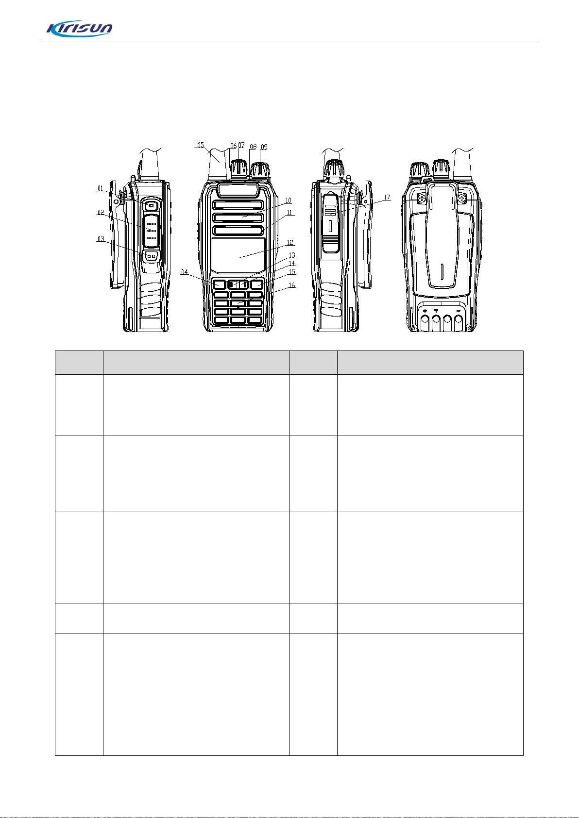
2. External View and Functional K eys
2.1. External View and Functional Keys
No. Part Name No Part Name
PTT(PUSH-TO-TALK)Button
01
03
05 Antenna 06
07
09
Side Button 1(Programmable
Button)
Side Button 2(Programmable
Button)
Channel Knob
Rotate to select chann el 1-16.
Power/Volume Switch:
Rotate the switch cl ockwis e to turn
on the radio, and
counter-clockw ise it until a click is
heard to turn off the radio.
Rotate the switch to ad just the
volume when the radio is
02
04
08 Top Key (programmable key)
10 Speaker
Press and hold the PTT button
and talk to the micropho ne to
transmit; release it to liste n.
Menu Key
Press the menu key and enter the
menu in the standby status.
During the menu operatio n, press
LED Indicator
The LED indicator glows r ed when
transmitting, and glows green
when receiving. The indicator
flashes red in the conditio n of low
Page 2 of 96
Page 6
FP560 S erv ice Manual
chapters for more details.
and edit the text or new cont act .
If the radio has multiple zones, the user could press the button to
Enable/Disable
feature.
repeater.
LCD Screen
11 Microphone 12
13 Up Key 14 Down Key
15 Delete Key 16
Spea ker/Microphone interface
17
Open the cover to connect the
external speaker and micr ophone.
It indicates the operation status of
the radio. Please see other
Digital Keyboard
There are 12 keys in tota l. Press
these keys to enter the number s
2.2. Programmable Button
You can require the dealer to program the keys listed below as shortcuts to certain functions for your
convenience:
• Long press key and short press key can be set: side button 1, side button 2
• Long press key can be set: menu key, delete key
Note:
• Short Press: Press and release it quickly.
• Long Press: Press and hold it down for 2 seconds, then r elease.
Available Functions Description
None No feature will be enabled.
Zone up
Zone down
Power Level Adjustment Switch to high/low power.
Squelch level adjustment Signal strength need ed w hen adjusting RX signal
Scan
Nuisance (temporary)
Delete
Digital Encryption
If the radio has multiple zones, the user can press the button to change
the zone from small to large.
change the zone from large t o sma l l.
Receives the activity of other channels. Press the button to switch
on/off the feature.
Delete the channel that is not c ur rently needed when scanning.
Enable/disable Encry pt ion on the channel that supports encryption
Channel Announce Announces the current channel.
Talkaround
VOX enable/disable Enable/disable VOX.
Select repeater/talkaround mode on the channel that allows using
Page 3 of 96
Page 7
FP560 S erv ice Manual
to the original status.
When this key is pressed, the sequelch feature will be invalid, and the
recover the sequelch feature.
Monitor Mementary
Monitor
If there is CTCSS on the curr ent analog channel, press the key and
switch to carrier squelch mo de t o cancel the CTCSS feature; the voice
will be output when the carr ier is matched. Release the key to go back
If there is CTCSS on the curr ent analog channel, press the key and
switch to carrier squelch mo de t o cancel the CTCSS feature; the voice
will be output when the carr ier is matched; press the key again t o go
back to the original stat us.
Sequelch off momentary
Cancel Squelch Disable Squelch to receive the weak signals on the analog channel
Emergency Alarm On Enable the emergency ala r m feat ur e t o seek help.
Emergency Alarm Off Disable the emergency al ar m feature.
VOX Electric Level
Selection
Battery Check Check the current battery power .
Whisper
user can hear the weak si gnal on the channel. Release the button to
Adjust the strength of VOX triggering electric l evel.
Enable/disable Whisper. The receiver can hear clearly when you speak
in a low voice when this feature is enabled.
2.3. LED I ndicator
• The LED lights up red when transmitting
• The LED lights up green when receiving
• The LED flashes red in the condition of low battery.
3. Circuit Description
3.1. Overview
This radio is FM portable equipment.
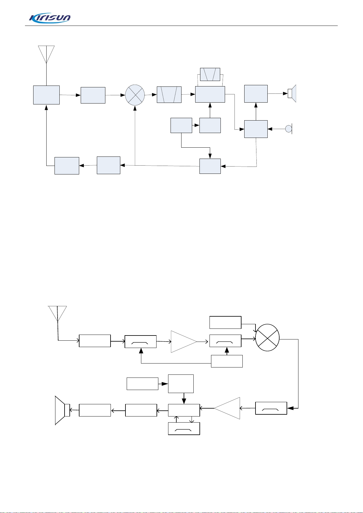
3.2. Fr equency Composition
Figure 3-1 Circuit Diagram
Page 4 of 96
Page 8
FP560 S erv ice Manual
ANT SW
RF
AMP
PA
AMP
TX
AMP
PLL
VCO
IF SYSTEM
X
4
multiply
TCXO
12.
8MHz
51
.65
MHz
MCF
CODEC
AF
AMP
MIC
CF
450
KHz
ANT
MIXER
ANT SW
BPF
1st local
osc
BPF
MCF
IF AMP
Q701
IF DET
450K
CODECAF PA
SPK
D600 D601
D602 D603
MIXER
Q702
Z1
51.65MHz
U6U800
ANT
X4
Multiply
Q300
TCXO
MCU
IC2
PC/TV
Q703
RF AMP
CF1
This Radio applies twice frequency mixing method. The first intermediate-frequency is 51.65MHz. The
second intermediate-frequency is 450kHz.
The first local oscillation is generated by frequency synthesizer, and the second local oscillation is
generated by the qcuadru ple frequency of 12.8MHz.
The transmitting signal is generated by frequency synthesizer.
The reference frequency of frequency synthesizer is generated by TCXO.
3.3. Pr inciple of Receiver ( R X)
Figure 3-2 Principle of Receiver
Page 5 of 96
• Receiver Front End
Signals from the antenna through the receiving/transmission (RX/TX) switch (D600, D601, D602, D603),
Page 9
FP560 S erv ice Manual
BT
SW
D402
AMP
Q602,Q603
DRIVE AMP
Q601
FINAL AMP
Q600
ANT SW
D600,D601
LPF
D602
RX
VCO
APC
IC600
DET
SW
Q604,Q605
APC
R620,R621,R622
ANT
5T
5T
which passed the band-pass filter (BPF) consisting of two levels o f LC t o eli minat e the unne cess ary signals,
then sent to the low noise amplifier (LNA) consisting of Q703 and its peripheral components for
enlargement.
After passing the band-pass filter (BPF) consisting of three levels of LC to further eliminate the
unnecessary out-of-ba nd signals, the output of LNA is then se nt to the first frequency mixer (Q702).
• The First Frequency Mixer
The signal from LNA is mixed with th e first loca l osci llator signa l fr om the freq uency sy nthes izer t o ge ner ate
the first intermediate-frequency signal (51.65MHz).
• IF Circuit
The first intermediate-frequency signal eliminates the signals from the adjacent channels or other signals
through the crystal fi lter. (Z1)
The first intermediate-frequency signal from the crystal filter, after being amplified by the first
intermediate-frequenc y (IF) amplifier (Q701), is sent to IF processing IC (IC7 00, GT3136).
IF IC consists of the second frequency mixer, IF amplifier, amplitude limiter, frequency detector, noise
amplifier, audio low pass filter.
The 12.8MHz signal from X300, being amplified by Q300 and its peripheral circuit, becomes the second
local oscillation signal (51.2MHz). The second local oscillation signal (51.2MHz) mixes with the first
intermediate-frequency signal (51.65MH z) in IC700 to generate the second intermediate-frequency signal.
The second intermediate-frequency signal amplified in IC700 with its amplitude being limited, being filtered
by the FD1 ceramic filter (450 k Hz ) , is dem odulated by IC700 to generate the audio signal.
• Squelch Circuit
The signal demodulated by IC700 is sent to its own noise amplifier for amplification, and the amplified
signal is sent to Q700 for f urther ampli ficatio n and to D70 1 for det ectio n; the produc ed direct current is t he n
sent to MCU squelch contr ol circuit, and its voltage is inversely propor t ion al t o the input signal.
3.4. Principle of Transmitter (TX)
Figure 3-3 Diagram of Power Amplification and Antenna Switch Principle
Page 6 of 96
Page 10
FP560 S erv ice Manual
PLL
DATA
Q301
RF AMP
LPF
Q302
RX VCO
PLL
DATA
Q303
BUFF AMP
12.8MHz
TCXO
X300
IC300
PLL IC
Q307
TX VCO
Q305,Q306
SW
Q304
RF AMP
MCU
The modulated RF signal from VCO, being ampl ified by Q303、Q304、Q602、Q603、Q601, is sent to Q600
for power amplification.
The grid bias of Q601 and Q600 is controlled by APC (Automatic Power Control) circuit. Change the grid
bias voltage to easily c ont r ol the out put power strength of the transmitter.
• APC
(Automatic Power Control)Circuit
R620, R621 and R622 are power amplifier current detection, and IC600A is a power amplifier current
sampling amplifier. IC600B is a power comparis on amplifier.
The extra high output power of the transmitter will increase the power amplifier current and IC600A output
with a decrease in IC600B output voltage. It will also decrease the bias voltage on Q601 and Q600, which
decreases the output power of the t ransmitter, and vice versa. This enables the stability of the output power
in different working circumstances.
MCU changes the volt age being input to IC600B to set the power.
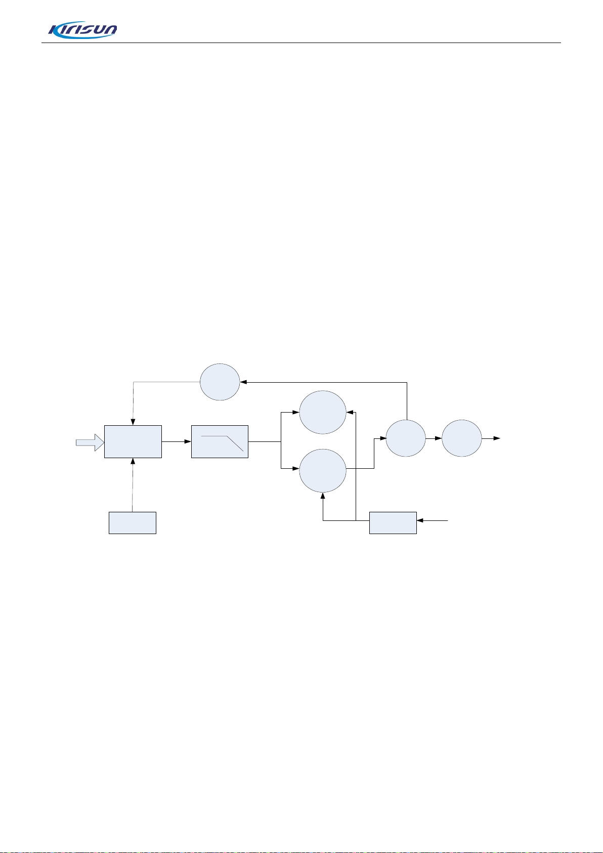
3.5. Pr inciple of Frequency Synthesizer
Figure 3-4 Diagram of Frequency Synthesizer
This radio applies PLL frequency synthesizer.
The frequency synthesizer consists of reference oscillator, voltage controlled oscillator (VCO),
programmable frequency divider, phase comparator and low pass filter.
Q307, D305, D306, D307, D308 and other resist ance-cap acit anc e units make up the t ransmitt ing VCO unit .
D304 is the modulation circuit of the transmitting VCO.
Q302、D300、D301、D302、D303 and other resista nce-cap acita nce units make up the receiv ing VCO unit.
IC300 (MB15E03) is a PLL integrated circuit which contains a programmable reference frequency divider,
programmable frequency divider, phase comparator and charge pump.
R329, C358, R330, C359, R331, R332 and C360 make up the loop filter.
The reference frequency is provided by X300 (TCXO, 12.8MHz).
Page 7 of 96
The reference frequency from TCXO (Temperature Controlled Crystal Oscillator) is divided by the
Page 11
FP560 S erv ice Manual
FM receiver
FM modulatorPA
TR
SW
Host MCU
4FSK
Protocol
stack
Voice
coder
U6 CODECL
U6 CODECR
ANT
SCT3252
U1
IC2
SPK
MIC
programmable reference frequency divider in IC300 to become the 5kHz or 6.25k Hz (controlled by MCU,
according to the setting channel) reference frequency .
The oscillation frequency from VCO, being amplified by the two-time frequency m ultiplier circuit, is sent to
IC300 for comparison with reference frequency after being divided by the programmab le fre quency divider,
and the error signal is then generated to change the oscillation frequency of VCO after filtered by the low
pass filter. VCO is locked when the frequency of VCO r eaches a certain set value.
Loss of Lock Detection: When PLL loses its lock, IC300 pin14 outputs the electric level signal to MCU, and
MCU control transmitter forbids transmitting and issues an alert tone. The output voltage of IC300 pin14 is
high electric level when it is loc ked.
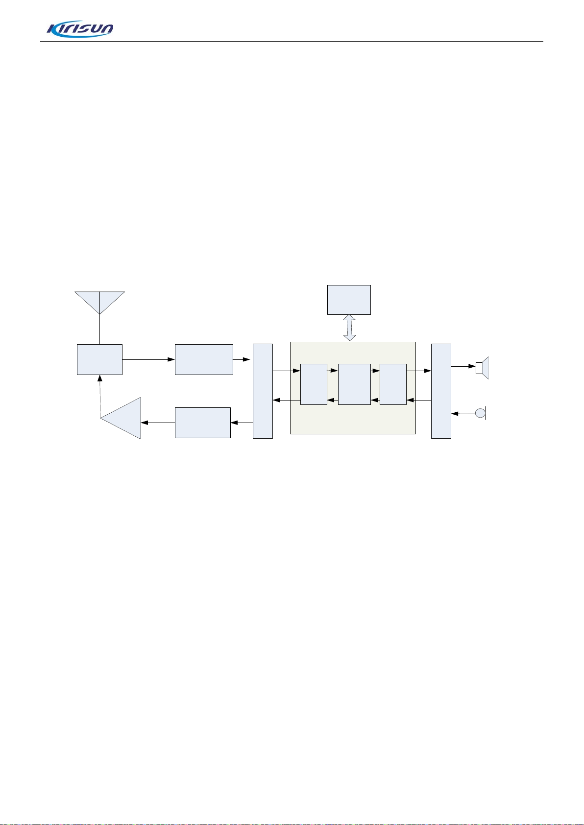
3.6. Audio Processing Circuit
Figure 3-5
• MIC Signal Processing
The speech signal from MIC is sent to U6 for A/D switch, and sent to U1 SCT3252 for audio
coding/decoding, communication protocol processing, channel coding modulation. Afterwards, the si gnal
outputs MOD2 and MOD1 separately from U6, and then sends them to TCXO and VCO for two-point
modulation. The signal outputs 4FSK modulating signal in digital state, and sine wave signal in analog
state.
• Receiving Audio Si gnal Processing
The audio signal demodulated from IC700 is sent to U1 SCT3252 for processing after finishing A/D switch
by U6. Af ter t he audio en c oding/ decod ing, co mm uni cation pr otoco l proce ssi ng and D SP, the audio signal is
sent to U6 for D/A switch, and it is then output to the U800 (TDA2822) audio power amplifier for
amplification so as to sound the s peaker.
Squelch Circuit:It is output fro m IC700 a fter d emod ulation, a nd it filters out th e noise fro m the d emodulat ed
signal after going through the filter circuit. It is sent to MCU after being detected by D701 and amplified by
Q700. The MCU ident ifies the noise level and cont r ols t he squelch.
Speaker Impedance: 16 Ω
Note: Any terminal of the speaker must not be attached to the gr ound!
Page 8 of 96
Page 12

FP560 S erv ice Manual
The emergency alert tone is not controlled by volume.
3.7. Power Supply
This radio applies 7.4V battery. The transmitter power amplifier circuit (Q601, Q600) and receiver audio
processor (U800) directly use the battery for power supp ly with ot her circuit s using the volt age st abiliz ed 5V
for power supply.
Q102: 5T switch, co nt r ol led by MCU.
5T: Supplies power for the transmitter front end.
Q100: 5R switch, controll ed by MCU.
5R: Supplies power for the receiv er RF ampli fier, frequency mixer , IF processo r, audio signal processor and
the like.
Q1: 5C switch, controlled by MCU.
5C: The 5V power source controlled by power saving, and it supplies pow er fo r frequency synthesizer unit.
3.8. MCU Unit
MCU unit controls every unit operation of the radio to perform all the radio functions.
• Communicates with the external PC
• Deposits and withdraws the radio status data
• Controls PLL to generate the local o s cillation frequency of receiving and transmitting
• Acquires the current channel status
• Controls the LED status indication
• Controls the power supply status of every unit
• Detects the operation of every function key
• Generates CTCSS signal
• Generates DCS signal
• Generates power-controlled signal
• Completes CTCSS decoding
• Completes DCS decoding
• Squelch detection and control
• Controls the content of voice prompt
Memorizer(E2PROM,AT24LC512BN)
It stores the radio channel data, C TCSS/DCS data, other function setting data and parameter adjustment
Page 9 of 96
Page 13
FP560 S erv ice Manual
No.
Frequency [ Hz]
No.
Frequency [Hz]
No.
Frequency [ Hz]
No.
Frequency [ Hz]
1
67.0
11
94.8
21
131.8
31
186.2
2
69.3
12
97.4
22
136.5
32
192.8
3
71.9
13
100.0
23
141.3
33
203.5
4
74.4
14
103.5
24
146.2
34
210.7
5
77.0
15
107.2
25
151.4
35
218.1
data.
CTCSS/DCS Signal Encoding and Decoding:
The CTCSS/DCS signal gener ated by MCU is sent separately to VCO and TCXO for modulation.
The CTCSS/DCS signal from the receiver is sent to MCU for decoding. The MCU identifies whether the
CTCSS/DCS signal of the r adio is t he same as the receiving signal so as to turn on the speaker.
CTCSS
CTCSS (continuous ton e contr ol squ elch s yst em) is a sque lch cont ro l syst e m modulated on the car rier wit h
the CTCSS signal being the pilot frequency. If the CTCSS feature is set, the conversation is enabled only
when the CTCSS frequency from the receiver and transmitter is the same to avoid interference from other
signals.
39 groups of stan dar d CTCSS frequency of this radio are available. See Chart 1.
CTCSS signal is generated by MCU (PWM wave form), and it is sent to VCO for modulation after being
filtered by the low pass fi lter composed of RC for eliminating the frequency higher than 300Hz.
Chart 3-1 CTCSS Frequency Chart
6 79.7 16 110.9 26 156.7 36 225.7
7 82.5 17 114.8 27 162.2 37 233.6
8 85.4 18 118.8 28 167.9 38 241.8
9 88.5 19 123.0 29 173.8 39 250.3
10 91.5 20 127.3 30 179.9
DCS Signaling:
DCS (Digital code squelch) is a continuous numerical code which is modulated along with the speech
signal on the carrier to control the squelch. If the DCS feature is set, the speaker is on only when the same
DCS code is received to av oid the unnecessary signal interference.
83 kinds of standard co de of this radio are available. See chart 2.
DCS signal i s generated by MCU (PWM wave form), and it is sent to VCO and TCXO for modulation after
being filtered by the low pass filter composed of RC for eliminating the frequency higher than 300H z. VCO
modulates the high freque ncy of DCS signal and TCXO modulates the low frequency of DCS signal.
CTCSS/DCS signal from the receiver is sent to MCU f or decoding. MCU identifies whether the receiving
signal has the same DCS code a s t he r adi o s o as t o turn on the speaker.
Page 10 of 96
Page 14
FP560 S erv ice Manual
043
132
244
364
506
703
054
152
261
411
546
731
071
156
265
413
606
734
073
165
306
431
624
754
output
output/power control (V)
2
DTMF
D/A Output
DTMF/Tone output, beep output
3
HSDI
I
Tone decoding input
10
RESET
I
CPU reset input
11
XOUT
O
CPU clock output
12
VSS
-
Gnd
19
SCLK
O
AK2346 data transm is sion clock
Chart 3-2 DCS Coding Chart
023 114 174 315 445 631
025 115 205 331 464 632
026 116 223 343 465 654
031 125 226 346 466 662
032 131 243 351 503 664
047 134 245 365 516 712
051 143 251 371 532 723
065 155 263 412 565 732
072 162 271 423 612 743
074 172 311 432 627
3.9. Se m iconductor De vice D escription
MCU Description
Chart 3-3 Microprocessor (M30620) Port Description
Pin No. Port Name Input/
1
4 EPDT I/O EEPROM data input/ output
5 EPCK O EEPROM clock
6 BYTE I Gnd
7 CNVSS I Gnd
8 BSHIFT O Clock beat frequency control
9 SV O Min. volume control
PCTV D/A Output
Function
Receiver sensitivity adju sting voltage
13 XIN I CPU clock input
14 VCC - +5V
15 NC I +5V
16 VDET I Voltage down detection
17 RDT I AK2346 MSK signal input
18 TCLK I AK2346 MSK data transmission clock
Page 11 of 96
Page 15
FP560 S erv ice Manual
20
CTCSS/DCS
I/O
CTCSS/DCS output
21
TDATA
O
AK2346 MSK data transmission output
28
CTCSSTCXO
O
CTCSS/DCS outputs ( PWM)
29
TXD
O
TXD1 output
30
RXD
I
RXD1 input
31
NC - NC
38
TX SW
O
Transmitter VCO switch
39
NC - Gnd
40
PLL UL
I
Phase-locked loop loss of lock check pin
41
PLL ST D
O
Phase-locked loop enabling control
48
EN3
I
Encoding switch input pin
49
EN4
I
Encoding switch input pin
50
EN5
I
Encoding switch input pin
51
W/N R1
O
Receiving IF bandwid t h switch
57
A SCLK
O
Number reporting chip clo ck
58
A MUTE
O
Number reporting chip control
59
NC - NC
60
ACC
-
+5V
61
NC - NC
22 StCtrl O Side tone volume contr ol pin
23 DI/O I AK2346 data input output control pin
24 CTCSSVCO O CTCSS/DCS output VCO (PWM)
25 DIR O AK2346 IO control
26 APC O Power control (U)
27 NC - NC
32 APC SW O Power control output switch
33 TXD0 O Extension
34 RXD0 I Extension
35 DC SW O Power control switch
36 TX W/N O Transmission bandwidth switch
37 RX SW O Receiv e r VCO switch
42 PLL DATA O Phase-locked loop data output
43 PLL CLK O Phase-locked loop clock
44 NC - NC
45 RX W/N O Receiving bandwi dth switch
46 EN1 I UV band selection
47 EN2 I Encoding switch input pi n
52 W/N R2 O Receiving IF bandwidth switch
53 AFCON O Audio power amplifier enabling control
54 RX MUTE O Receiving mute switch
55 A BUSY I Number reporting chip control
56 A DATA O Number reporting chip data output
62 VSS - Gnd
63 NC - NC
64 SELF - Factory control optio ns
Page 12 of 96
Page 16
FP560 S erv ice Manual
65
OPT S1
I
Earphone check
66
OPT S2
I
External PTT
73
PTT
I
PTT key
74
SK2
I
Side key 2
75
SK1
I
Side key 1
76
SP SW
O
Speaker switch
83
P03
O
Fixed side tone control
84
P02
O
Phase-locked loop filter
85
NC O NC
86
NC - NC
96
VREF
-
+5V
97
AVCC
-
+5V
98
NC - NC
99
MIC MUTE
O
External and internal MI C swit ch
100
HPF PC
O
High pass filter switch
IC202
PST9140NR
MCU reset circuit
U300
MB15E03
Frequency synthesizer
IC600
NJM2904
APC, voltage comparisom, drive
67 MAN DN I MAN DOWN input
68 PIO3 I/O Extension
69 PIO2 I/O Extension
70 PIO1 I/O Extension
71 PINT I Extension
72 TK1 I Top key
77 MIC SW O MIC switch
78 R LED O LED red switch
79 G LED O LED green switch
80 5T C O 5T control pin
81 5R C O 5R control pin
82 5C C O 5C control pin
87 MAN DOWN I Reverse detection input
88 BATT I Voltage chec k input
89 RSSI I Receiving filed intensity signal input
90 BUSY I Squelch voltage check input
91 VOX I VOX voltage check input
92
CTCSS/DCS
IN
I CTCSS/DCS input
93 DTMF IN I DTMF input
94 AVSS - Gnd
95 NC - NC
Chart 3-4 Semiconductor Device Feature Description
Position No. Item No. Feature Description
Page 13 of 96
Page 17
FP560 S erv ice Manual
IC2
M30620
MCU
Q302
2SK508NV
RX VCO oscillator tube
Q300
2SC5108
RX 2nd local oscillation amplifier
Q307
2SK508NV
TX VCO oscillator tube
Q601
RD01MUS1
Transceiver power amplifier drive
Q600
RD07S2B
TX final power amplifier
Q602
2SC5108
Transceiver 1st amplification
Q700
2SC4617
Receiver noise amplifier
Q800
FMMT717
Audio output control switch
Q801
DTC144EE
Audio power amplificati on control switch
IC100
XC6204B502MR
Adjust output of 5C regulated voltage
D309
DA2S10100L
Losing lock detected) diode tube
D307,D308
D402
HSC277
VCO output switch
IC700 GT3136 Receiver 2nd local oscillation, 2nd IF amp li fic at i on, amplitude
limit, demodulation, nois e am plification
IC204 NJM2902 Receiver demodulated signal is amplified, f ilter
IC200 AT24C512C E2PROM, saving channel frequency data, feat ur e setting
parameters and adjus tment status parameters.
U800 TDA2822 Receiver audio power amplification
Q304 2SC5108 VCO buffer amplifier
Q305 DTA143TE TX VCO control switch
Q301 2SC5108 Feedback loop ampl ifier
Q306 DTA143TE TX VCO control switch
Q308 2SC4617 VCO power filter
Q303 2SC5108 VCO buffer amplifier
Q603 2SC3356 Transceiver 2st amplification
Q604 DTA144EE APC output switch
Q703 3SK318 Receiver low noise amplifi er
Q702 3SK318 1st frequency mixer
Q701 2SC5108 IF amplifier
IC100 XC6204B502MR Adjust output of 5R regulated voltage
IC100 XC6204B502MR Adjust output of 5T reg ulated voltage
IC102 XC6228D122VR 1.8V output adjustment
IC101 XC6204B332MR 3V output adjustment
Chart 3-5 Diode T ube Feature Descript ion
Position No. Item No. Feature Description
(
D310 DA2S10100L VCO power filter acceleration diode
D304 1SV278 TX VCO modulated diode
D305,D306
HVC376 TX VCO oscillation varac t or diod e
D300,D301
HVC376 RX VCO oscillation varactor diode
D302,D303
Page 14 of 96
Page 18

FP560 S erv ice Manual
D604
HZU5ALL
APC output limited voltage diode
D704,D705,D
D708
HVC355B
RX band pass filter var actor diode
D701
RB706F
Commutation diode
D600,D601
D602,D603
706,D707
HVC131 Transmitter ant enna switch diode
4. Function Description and Parameter Settings
4.1. Time-out Timer
This feature prevents t he user from long occupation on the cha nnel. If the transmitting period exceeds the
dealer’s preprogrammed time, the radi o stops transmitting and rings alert tone. To stop the alert tone,
please release the PTT button. For a second transmission, please press the PTT button after a certain
period (set by the dealer). If the dealer preprograms the pre-warning feature, a warning is given when the
transmitting period gets close to its time-out-timer limitation, indicating the t r ansmission is forbidden soon.
4.2. Channel Scan
The channel scan is able to search for the channel where there is a signal, and the radio stays on the
channel where a signal is detected f or making a conversation. The scanning mode is the carrier control
scan.
4.2.1. Carrier Control Scan
The radio scan stays on a busy channel until it is no longer busy, and the scan is enabled automatically
after a certain per i od ( t he specific period time is set by the local dealer).
Press the Scan shortcut key, and the radio scans the scan list of the current channel. When the radio is
scanning, you can press t he “ Scan” shortcut key to stop the scanning.
4.2.2. Scan Reply Channel
When the radio is scanning, press the PTT button to transmit and make a conversation on a preset
channel, and the channel is pr epr ogrammed by the local dealer.
4.3. Kill and Activation
If the dealer preprogram s this feature, the radio can receive and decode other radio’s signals of kill and
activation before respondi ng accor dingly. After bei ng killed, the radio can only receive the activated signal
without being able to transm it or r eceive other signals. The radio is back to normal a f t er act ivation.
Page 15 of 96
Page 19

FP560 S erv ice Manual
4.4. Emergency
In a state of emergency, press the “Emergency On” button (the button is programmed as the “Emergency
On” button) for the alarm call. To disable the emergency feature, please press the “Emergency Off”
shortcut key or restar t t he r adio.
The alarm method is compos ed of two parts:
• Alarm type: mainly specifies the acoustooptic r eaction in the state of alarm call.
• Alarm mode: specifies the content sent in the state of alarm call. You can set these parameters through
the dealer to meet your requirements.
Alarm Mode:
• None: No alarm feature (by default), and the alarm f eature cannot be enabled by pressing the
emergency button.
• Siren Only: The radio only emits siren locally.
• Regular: The acoustooptic alert can be enabled, and the radio is able to receive.
• Secret: No acoustooptic alert and the radio is not able to receive.
• Secret but receivable: No acoustooptic alert but t he r adio is able to receive.
Alarm Mode:
• Emergency Alarm: After the alarm feature is enabled, the radio only transmits an emergency alert , and
afterwards, then automatic exit the alarm status.
• Emergency Alarm + Emergent Call: The radio transmits an emer gency alarm and sends out an
emergency call by pressin g t he PTT button.
• Emergency Alarm + Auto Transmission of Backgrou nd T one: The radio transmits an emergency alarm,
and the background tone will be sent out periodically and automatically in the way of emer gency call.
Note:
• Emergency Alarm: A non-speech signal transmitted by the radio t o in form other radios to send out an
alert.
• Emergency Call: A call mode in the priority of using the channel to ensure a successful call during
emergency.
4.5. Pa rameter Settings
The radio is preset before the factory delivery, but the parameter of the digital feature, operational
frequency, channel, QT/DQT, and auto scan feature may be reset according to different requirements of
the customers. Hence, Kirisun designed a Chinese/English FP520 programming software with friendly
interface, easy operation and c l ear visual display to complete the parameter s et t ings for FP520.
Procedure of setting the parameter with a computer.
A. Install the FP520 programming software on the computer.
Page 16 of 96
Page 20
FP560 S erv ice Manual
Computer
cable
Radio
B. As Figure 4-1 shows, using the FP520 programming cabl e t o c onnects the computer with the radio
Note: During the connect i on, ① make sure the computer is off. ② make sure the radio is off.
Figure 4-2
C
.Turn on t he computer.
D.Turn on the Radio.
E.Click the execution procedure, and operate FP520 programming soft ware.
F.In the main menu of FP520 programming software, click ”read” menu to input the r adio parameter into
the computer.
G.For detailed operation, please refer to the ”assistance” file of t he progr amming software.
FP560 programming
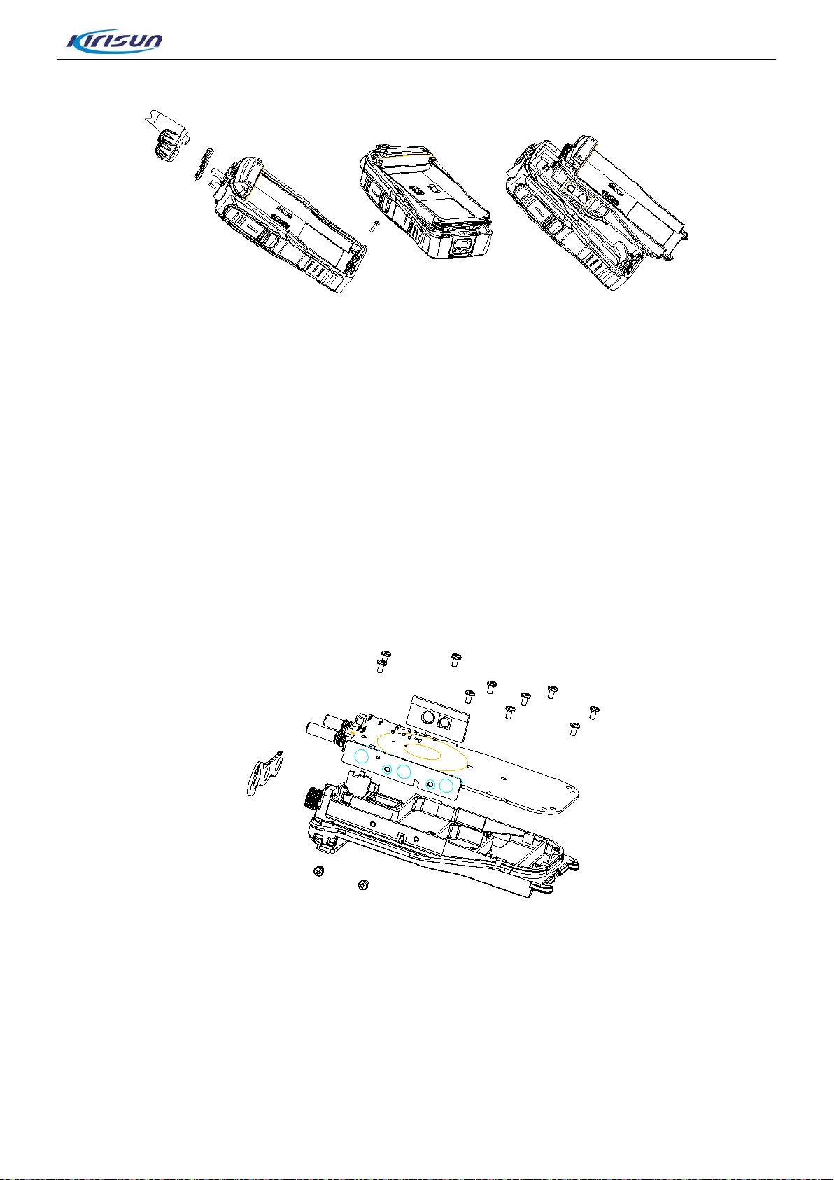
5. Assemble and D isassemble In structions
This radio is sophisticated communication equipment with a precise and compact mechanism. The
assembly and disassem bl y of the radio must be carefully done during the rep air.
The description is as follo ws:
5.1. Attaching and Detaching the Battery
Attaching the battery
Press ① to bounce the belt clip; align the two bulges on the battery top with the corresponding slots on
the aluminum shell, and insert t he bat t er y into t he aluminum shell in the direction as ② shows. Press the
battery bottom as ③ shows to completely bounc e t he latc h, and the b at tery is att ached unt il the bat tery is
hooked as ④ shows (see Figure 5-1).
Figure 5-2
Detaching the Battery:
Make sure the radio is of f when detaching the battery.
To detach the battery, please push the battery latch as ① shows to bounce the bottom of the battery as
Page 17 of 96
Page 21
FP560 S erv ice Manual
② shows, and take out the battery as ③ shows; if the belt clip is attached, please press it as ④ shows
and detach the batter y downwards.
Figure 5-3
Notes:
• Do not short circuit the battery terminals or abandon the battery into fire.
• Do not take the risk of disassembling the batt er y shell.
5.2. Attaching the antenna
When attaching, put the antenna end with screw thread into the threaded hole of the radio top, and turn it
clockwise until it is fastened.
For detaching, hold the an t enna bot tom and turn it counterclockwise.
Figure 5-4
5.3. Attaching and Detaching the Belt Clip
When attaching, align the screw holes of the belt clip wi th the corresponding ones of the radio back shell,
and use two 2.5x8.0 machine screws to fasten.
Loosen the two 2.5x8.0 machine screws to detach the belt clip.
Page 18 of 96
Page 22
FP560 S erv ice Manual
Figure 5-5
5.4. Attaching and Detaching the Earphone
When the earphone is needed, open the earphone cover on the upper right side of the radio, and put the
earphone plug into the interface.
Figure 5-6
5.5. Se parating the Front Cover from the Chassis
1. Remove the antenna, v olume knob and channel knob;
2. Remove the two knob nuts and one antenna nut;
3. Remove the two aluminum screws with wabblers;
4. Use a pair of tweezers or ot her t ools t o l ever open the bottom;
5. Pull out the Front Cover ;
6. Use an electric soldering iron to cut off the speaker wire and MIC wire, and t he separation is done.
Figure 5-7
Page 19 of 96
Page 23
FP560 S erv ice Manual
5.6. Se parating the PCB Board from the Cha ssis
1. Remove the potentiomet er waterproof pad on top;
2. Remove the earphone wat er pr oof plug;
3. Remove the screws on the PCB ma inb oar d;
4. Remove the two screw s on t he side PTT PCB;
5. Use an electric soldering iron to cut off the antenna terminal and the PCB board is removed. (PTT PCB
is connected with the P CB mainboard. To avoid bonding pad damage, use an electric soldering iron to
separate them instead of dividing them with force)
Figure 5-8
After the disassembly above is completed, the repair and adjustment can then be done.
Page 20 of 96
Page 24
FP560 S erv ice Manual
No.
Part Number
Description
Quantity
Remark
keypad
frame
5.7. Ex ploded View
1 7MHR-4091-01A-W0
2 7MHP-7208-06A-W0
3 7MHP-7208-07A-W0
4 7MHJ-4091-01A-W
5 7MBP-4091-01A-WC FP560 lens 1 PC, silk print black frame
6 7GCB-070001
7 7MHR-1727-09A-W3 558 mic cover 1 Silicone gel, hardness 40, orange
8 4SM7-6027-A40C MIC S760 780 1
FP560 digital
PT560 earphone
cover plug
PT560 earphone
cover board
FP560 lens
double-sided
adhesive tape
φ7 mic
waterproof cloth
1
1 ABS+PC;black
1 TPU;black
1 3M9448
1
Silicone gel+plastic key+plastic
waterproof cloth,diameter φ7mm,
thickness 0.1mm
Φ6.0, -40±2dB omni directional,
2.2KΩ,2V, with 80mm red black wire
Page 21 of 96
Page 25
FP560 S erv ice Manual
9
7MHP-4083-01A-W0
FP560 front shell
1
ABS+PC; black; silk print
PT560 guide
circlip
19
7MHP-7208-02A-W0
PT560 channel
1
ABS; black, white paint
3.5mm, black passivation
RF coaxial
waterproof plug
silicone gel pad
waterproof ring
10
11 7MHR-7208-05A-W3
12 7MHR-7208-04A-W9
13 7GCB-360001-W0
PT560 LOGO
sticker
PT560 emrgency
button;
beam
φ36 speaker
wanterproof net
1 T=0.3mm PC
1 Silicone, orange
1 Silicone; transparent milk white
1 Black wanterproof cloth
14 4SS7-4050-016-100 ∅ 40 speaker 1 MM4050-1638,16Ω,1W
PT560 side
15 7MHR-7208-06A-W0
silicone gel
1 Silicone; black
button
16 7MHP-7208-05A-W0
17 7MHS-1140-01A-W
18 7MHP-7208-01A-W0
PT560_PTT
cover board
3118/3208 knob
PT560 volume
knob
1 ABS+PC, black
2 Spring steel
1 ABS; black, white paint
20 PT558S antenna 1
21 7NRC-090136039-B1 558 antenna nut 1
22 7NRC-060100035-B1
23 7MHR-7208-02A-W0
24 3CR7-SMA-50JFB-4
558 switch nut
PT560 top
waterproof ring
connector
2
1 Silicone; black
1 SMA-J, flang plate installation
PT560 earphone
25 7MHP-7208-04A-W0
socket
1 TPU; black
Thermally
26 7MHR-7042-06B-W0
27
7SMF-020037M-SZCT
-N
28 7MHR-7208-01A-W0
conductive
M2.0*3.7 cross
sunken machine
screw
PT560 major
1 Silicone, black,3*6*9mm
2 Screw for fixing PTT PCB
1 Silicone; black;polished
Diameter
14mm
brass, internal diameter
M9mm,external diameter φ13.6mm,
thickness 3.9mm, black passivation
brass, internal diameter M6mm,
external diameter φ10mm, thickness
29 7MHR-4083-01A-W0
FP560 pedestal
waterproof pad
Silicone, black, hardness 60 degrees
Page 22 of 96
Page 26
FP560 S erv ice Manual
torsional spring
M2.5*8 cross
machine screw
35
7MJP-4026-01A-W0
KBJ-15 belt clip
1
DP770 belt clip,PC+ABS, black
top shell
bottom cover
alloy shell
PCB
52
7MHX-7042-02A-Z
battery hook 1
1
Zinc alloy (Zn3#), cat apho resis, black
53
7STF-019047B-SZHT-
M1.9*4.7 cross
3
Fixing LCD hardware bracket
30 7MHP-4091-02A-W0
31 7MJS-7013-01B-N
32 7MJS-7013-02A-W
33 7MJS-7013-03A-N
34
7SMF-025080M-SZYB
-Z1
36 7MDP-7208-01A-W0A
37 6PD7-7215-DPA
38
6BLM-103445-074150
-A
39 7MDP-4083-03A-W0A
PT560 main unit
top cover
KBJ-09 belt clip
bracket
KBJ-09 belt clip
KBJ-09 belt clip
spin axis
round flat head
FP560 battery
FP560 charging
PCB
FP560 battery
chip
FP560 battery
1 ABS,+PC black
1
Stainless steel ;(SUS304),1.00THK,
bright nickel-plated
1
1
2 For fixing belt clip
1 ABS+PC
1 Thickness 0.6MM
1 li-ion 1500mHA
1
40
7SMF-020080M-MHH
T-N1
41 7MHL-4083-01A-W
M2*8 torx thick
–headed
machine screw
FP560 aluminum
2 For fixing aluminum shell
1 ADC12
FP560 PTT
42 7MHS-4083-01A-W
button metal
1 φ6mm,SUS301 square metal dome
dome
43 FP560 PTT PCB 1
44
45 3WF7-05030-500C4
46
7SMF-020040M-SZYB
-N
47 7MHS-4091-01A-W
FP560 MAIN
Flex cable(with
radar absorption
cotton)
M2*4 cross
round flat head
machine screw
FP560 LCD
bracket
1 Thickness 1.2mm
1
13
Interval 0.5mm,30P, wire length
50mm
Fixing main board, PTT keypad and
antenna screw
1 Stainless steel (SUS304),0.3THK
48 7MHS-7042-01B-W latch 2 1 Stainless steel (SUS301),0.25THK
49 7MHS-7042-01A-W latch 1 1 Stainless steel (SUS301),0.25THK
50 7MHP-7042-14A-W0 battery lat ch 1 POM,black
51 7MHX-7042-02B-Z battery hook 2 1 Zinc alloy (Zn3#), cataphoresis, black
Page 23 of 96
Page 27
FP560 S erv ice Manual
sponge pad
keypad PCB
FP560
X round flat
machine screw
54 6MD7-F04932 FP560 LCD 1
55 7GCM-411294-J
56 7MHJ-4091-01A-W
57 7MHR-4091-01A-W0
58 7MHS-4091-02A-W
FP560 LCD
FP560 keypad
double-sided
adhesive tape
FP560 digital
FP560 digital
keypad metal
dome
Black and white screen
,128*64
1 PRON, 41.1*29.4mm
1 3M9448
1 Thickness 0.6mm
1
SUS301,Φ5mm Metal Dome
6. Adjustment
6.1. Components of Adjustment
During the service, a proper test and adjustment to the radio’s technical criteria is necessary after
changing the components.
6.1.1. Components needed for the adjustment
(1) antenna interface conv er tor
(2) universal interface
6.1.2. Manual Mode Adjustment
The radio needs adjustme nt of 5 frequencies.
The frequencies selected by the channel switch are shown in the chart below:
Model Channel 1 Channel 2 Channel 3 Channel 4 Channel 5
FP560
VHF
UHF
136.05MHz 145.55MHz 155.05MHz 164.55MHz 173.95MHz
400.05MHz 415.05MHz 435.05MHz 455.05MH 469.975MHz
Page 24 of 96
Page 28

FP560 S erv ice Manual
6.1.3. Computer Adjustment Method
VCO Part
The radio is receiving:
a) The channel is on the r eceiving high frequency, adjust C335 and test T300, the spot voltage i s 3.6 ±
0.1V.
b) The channel is on the r eceiving low frequency, t est T300, the spot voltage>0.6V
The radio is transmitting :
a) The channel is on the t r ansmitting high frequency, adjust C371 test T300, spot volt age as 3. 6± 0. 1V
d) The channel is on the t r ansmitting low frequency, test T300, the spot voltage>0.6V
TX Part
1). Transmitti ng Frequency
Under the computer mode, the transmitting frequency is adjusted within ±100H z.
2). Power
a. Under the computer mode (t r ansmitting high power) (5 frequencies), the transmitting high power is
adjusted to 3.8-4.2W.
b. Under the computer mode (t r ansmitting low power) ( 5 frequencies), the transmitting low power is
adjusted to 0.8-1.1W.
3). The Maximum Fre quency Deviation (the modulation signal is 1kHz/120 m V )
Under the computer mode [the maximum audio frequency deviation] (the broa dband has five frequencies
and the narrowband has one; six fr equencies in total), adjust the maximum transmitting frequency
deviation to 1.8-2.5 kHz.
4). DCS Balance
Under the computer mode, [DCS balance] (the broa dband has five frequencies), adjust the DQT and
make it balanced, so the demodulated DQT wave can be square and smooth.
5). DCS Frequency Deviation (DQT: 023N)
Under the computer mode [DCS frequency deviation], adjust DCS frequency to 0.3-0.5kHz.
6). CTCSS Frequency De viation(QT: 67.0Hz, 150.4Hz, 250.4Hz)
Under the computer mode [CTCSS (67Hz, 150.4Hz, 250. 4Hz) frequency deviation] adjust the CTCSS
frequency deviation to 0.3-0.5kHz.
7). DTMF Frequency Dev iation
Under the computer mode [ DTMF frequency deviation] (five frequencies), adjust the DTMF frequency
deviation to 1.5-2 kHz.
8). Battery low volt age indication when transmitting: the voltage is set as 6.8V,under the comput er mode
Page 25 of 96
Page 29

FP560 S erv ice Manual
[transmitting low volt age], click OK when the digits are stabilized.
RX Part
1). Receiver Pass Band
a. Program the spectrum analyzer, and test the receiver pass band at the test point with a high frequency
probe.
b. Under the computer mode [ rec eiv ing sensitivity] (five frequencies), adjust the receiver pass band to the
corresponding center frequency.
2). The Maximum Volume
Set the RF frequency as the cent er frequency, the signal strength as 1mV, and the modulated frequency
deviation as 1.5 kHz. Under the computer mode, set the computer audio power as 1. 1-1.3W.
3). First Level Squelch Adjustment
a. Set the RF signal as -121dBm and the modulated frequency deviation as 1.5 kHz . Under t he computer
mode (on) (five frequencies), c lick OK when the digits are stabilized.
b. Set the RF signal as -123dBm and the modulated frequency deviation as 1.5 kHz . Under t he computer
mode (off) (five frequ encies), click OK when the digits ar e stabilized.
4). Field Str ength
a. Set the RF signal as -121dBm and the modulated frequency deviation as 1.5 kHz . Under t he computer
mode (low RSSI) (five frequency points), clic k OK when the digits are stabilized.
b. Set the RF signal as -70dBm and the modulated frequency deviation as 1.5 kHz. Under the computer
mode (high RSSI) (five frequency points), click OK when the digits are stabilized.
6.2. Radio Test
The following criteria shou ld be tested:
RX Part
1. Sensitivity: <=-120dBm (0.25uV) 12dB SINAD
2. Distortion: <=5%
3. Current: static cur r ent : <=100mA
RX working current: <=400mA
4. QT/DQT decode: when <=-116dBm (0.35uV), the radio decodes correctly.
5. Sensitivity of the 3rd squelch off: when RF input ≤-124dBm时, the squelch should be turned off.
6. Sensitivity of the 3rd squelch on: when RF input ≥-119dBm, the squelch should be turned on.
TX Part
1. Output power: Hig h (3.8W---5W); low (0.9W---1.1W)
2. TX current: High power transmitting <= 1.6A; low power transmitting<=1.0A
Page 26 of 96
Page 30
FP560 S erv ice Manual
3. The maximum fr equency deviation: 1.8kHz---2.5kHz
4. TX distortion: <=5%
5. QT/DQT frequency deviation: 0.3---0.5kHz with fine wave form.
6. TX frequency deviation: Nominal frequency +/-500Hz
7.DTMF frequency deviation: 1.5~2.0 kHz
8. FFSK frequency deviation: 1050Hz+/-50
9. Under voltage Ind ication: The voltage is 6.6V, the indicator glows red when PTT is pressed; no TX
power.
7. Major Specifications
General Specificatio n
Model FP560
Frequency Range UHF: 400-470MHz VHF: 136-174MHz
Modulation Method 4FSK
Channel Capacity 256
Channel Spacing 6.25kHz/12.5kHz
Intermediate Frequency The first IF: 51.65MHz the second IF: 450kHz
Operation Voltage 7.5V negative pole is connected to the ground
Operation Temperature
Antenna Impedance 50Ω
-25℃~ +55℃
Microphone Impedance 2.2kΩ
Battery (Standard) Li-ion battery DC 7.4V , 1500mAh, duration:12.5 hours
Dimension 118.2mm x55.7mmx32.9mm
Weight
270(with battery and ant enna)
Page 27 of 96
Page 31

FP560 S erv ice Manual
RX Part
Sensitivity (12dB SINAD) ≤0.25μV
Squelch-On Sensitivity ≤0.18uV
Receiver Residual Output ≤-35dB
Modulated RX Bandwidth ±3.5kHz
Adjacent Channel Selectivity ≥50dB
Intermodulation Interference
≥65dB
Rejection
Spurious Response Rejection ≥70dB
Audio Output Power 1.3W, BTL@distortion≤10%, 16Ω
RX Consumption Current ≤400mA
TX Part
Tx Power 4.0W/1.0W@7.5V DC
Frequency Stability ≤ ±2.5ppm
The Maximum Modulated
±2.5kHz
Frequency Deviation
Modulation Distortion
≤ 3%
(300~3000Hz)
Adjacent Channel TX Power ≥60dB
Spurious TX ≥70 dB
Residual Modulated
≥40 dB
Frequency
TX Consumption Current ≤1.7A@7.5V DC
Page 28 of 96
Page 32

FP560 S erv ice Manual
8. Maintenance and Test Equipment
During the service and test , t he follow ing equipment and apparatus are needed.
Equipment Specification
Standard Signal Generator Frequency Range: 400- 470MHz
Modulation: FM and Exter nal Modulation
Output: -127dBm/0.1uv or ≥-47dBm/1mv
Power Meter Input Impedance: 50Ω
Operation Frequency : 400 - 470MHz
Measurement Range: about 10W
Deviation Meter Frequency Ra nge: 400-470MHz
Digital Voltmeter Measurement Range: DC 10mv - 10v
Input Impedance: high inp ut i mpedanc e for the minimu m circ uit loa d
Oscilloscope Frequency Range: DC - 30MHz
High Sensitivity Frequency
Counter
Ammeter Maximum Current: 5A
Audio Voltmeter Frequency Range: 50Hz - 10KHz
Audio Generator Frequency Range: 50Hz - 5KHz or higher
Spectrum Analyzer Measurement Range: DC - 1GHz or higher
Frequency Range: 50Hz - 10KHz
Frequency Stability: 0.2ppm or lower
Volt Range: 1mv - 10v
Output: 0 - 1v
Path Generator Center Frequency: 50KHz - 600MHz
Output Voltage: 100mv or higher
16Ω Dummy Load About 16Ω, 3W
Adjustable Power Supply 5v - 10v, about 5A
Page 29 of 96
Page 33

FP560 S erv ice Manual
9. KBC-51 Charger
9.1. The Operational Conditions and Ba sic Specification of Charger
a) Battery Specification:Li-ion(2*3.7V),battery capacity (1~2.4AH).
b)Power A daptor Specification: DC 1 1V~ 16V,500~1500mA power adaptor,standard voltage is 12V.
c) No-load Input Current: ≤ 15mA
d) Precharged Current: 200 mA±40 mA
e) Precharged Time Limit: 15Min
f) Constant Current Charging Current :800 mA± 40 mA
g) Maximum Li-ion Charging Vo ltag e:8.32~8.42V.
9.2. Function Int roduction
1. This charger is inte ll ige nt with fast charging, reliability, safety and high charging saturation.
2. St atus I ndicat ion: Th e indicat or flashe s red for pr echarg ing and lights red for charging; it lights green for
full charging, no battery and battery protection; it flashes yellow for battery output short circuit.
3. The external port id ent i fies the lithium battery .
4. Battery Short Circuit Protection: When there is a short circuit in the negative and positive pole of the
charger, the indicator flashes yellow and the charging current will be cut off. The charging will continue
automatically after t r oubleshooting.
5. The full battery is recharged for identification: When the full Li battery is recharged, if the voltage is
higher than 8.25V, the charging stops, and if it is lower than 8.25V, the charging conti nues.
6. Temperature Protection: When the Li-ion bat t er y is charging, the charging stops with the yellow light on
if the temperature is higher than 55 degrees. The charging is restarted when the temperature is down to
45 degrees.
7. Put the radio on the charger when it is on standby mode, and the charging automatically begins when
the battery voltage is lower than 8.2 V.
8. The yellow light indicates the charger automatic protection. The charging is restarted after the
troubleshooting.
Page 30 of 96
Page 34

FP560 S erv ice Manual
LED lights red: Chargi ng
LED lights green: Ful l battery
LED lights yellow: Abnormal charging
10. Troubleshooting
No. Problem Ca use and Solution
A.The battery pack may be out of p ower. Please charge it or
change to a new one, then try again.
1 Power-on Failure
PLL is unlocked
2
(beeping))
B.Power switch failure. Cha nge to a new power switch.
C.CPU failure. Change to a new CPU.
D.Protective tube F100 f ailur e. Change to a new protective tube.
A.The PLL crystal oscillator X300 is broken, please change to a
new one.
B.The oscillation tube is broken, please change to a new one.
C.The PLL chip IC300 is broken,please change to a new one.
3
Communication
Failure
A.The frequency is not the sa me. P lease reselect a channel with
the same frequency
B.The signaling codes of CT CSS/D CS are di fferent ,pl eas e reset
them with the computer.
C.Beyond the communication range.
Page 31 of 96
Page 35

FP560 S erv ice Manual
A.The antenna is in poor contac t,please fasten it again.
B.Low sensitivity,adjust the parameter in the “test mode”.
C.The high-mu tube Q703 is broken, please change it.
4 No Signal
No voice on the
receiving radio
5
when the indicator
glows red on the
transmitting radio.
No voice received
6
when the indicator
glows green.
D.The squelch level is to o high to turn it on, please adjust the
squelch level.
E.Mixer tube Q702 is broken, please change it.
F.FM processing chip IC700 is broke n, ple as change to a new IC.
A.The power amplifying t ube is broken with no power output,
please change it.
B.The microphone is broken, please change it.
C.The operational ampl ifier Q 601 is broken, please change it.
A.The speaker is broken, please change it.
B.The audio power amplifier U800 is broken, please change to a
new IC.
C.The switch diode Q801is broken, please change it.
A.Improper connection, please check the cable connection.
7
Abnormal
Programming
B.The computer serial p or t out put is abnormal, please check the
computer.
C.The earphone jack is in poor contact, please c heck it an d change
it if broken.
Page 32 of 96
Page 36

FP560 S erv ice Manual
Appendix 1 Abbreviation
AMP Amplify, Amplifier
ANT Antenna
APC Automatic Power Control
BPF Band Pass Filter
CTCSS Continuous Tone Control Squelch System
DCS Digital Code Squelch
DEMOD Demodulation
E2PROM Electrically Erasable Programmable Read-Only Memory
HPF High Pass Filter
IDC Instantaneous Deviation Control
IF Intermediate Frequency
LED Light-Emitting Diode
LNA Low Noise Amplifier
LPF Low Pass Filter
MCU Micro Control Unit
MIC Microphone
MOD Modulation
MONI Monitor
PLL Phase-Lock Loop
PTT Push-To-Talk
RX Receiver
SPK Speaker
TCXO Temperature Control Oscillator
TX Transmitter
UL Un-Lock
VCO Voltage Control Oscillator
Page 33 of 96
Page 37

FP560 S erv ice Manual
Accesoory
Quantity
User Guide
1
ty
charger KBC-51
vocoder)
tube
Appendix 2 Accessory List
Antenna 1
Adapter 1
Belt Clip 1
Intelligent Charger 1
Strap 1
Battery 1
Appendix 3
List 1 Spare Pare List (Electronic Section 400-470MHz)
Part Number Item Name Specification
FP560-02
6SS3-4109-AA
6SS1-4083-HMC
0SS1-4083-HMC
1DS1-HSC277
FP560-02 main
unit
FP520-02 main
unit SMD(
FP520-02 main
unit SMD(change
vocoder)
SMD switch diode
change
400-470MHz,4W,
400-470MHz,
6.25K,pb-free
FP520-02,,pb-free 1
FP520-02, pb-free 1
HSC277,1608 3 D402 D602 D700
Quanti
0
1
Plug-in Unit Postion
Page 34 of 96
Page 38

FP560 S erv ice Manual
23
D300 D301 D302 D303
D305 D306 D307 D308
D704 D705 D706 D707
P-8
OP-16
series
6.25K series
SMD specia lized
1DS1-HVC131
SMD switch diode
tube
1DS1-DA2S10100L SMD switch diode
tube
1DS1-RB706F-40
1DV1-1SV278
1DV1-HVC376B
1DZ1-HZU5ALL
SMD switch diode
tube
SMD varactor
diode tube
SMD varactor
diode tube
SMD regulated
voltage diode tube
1IL1-NJM2904V SMD linear IC
HVC131(P1),1608 2 D600 D601
DA2S10100L 3 D309 D310 D709
Schottky diode
RB706F-40,SOT-3
1 D701
1SV278(T1) 1 D304
HVC376B(B9) 13
D708
HZU5ALL,2012,5
V
1 D604
Dual operational
amplification
NJM2904V,TSSO
1 IC600
1IM1-AT24C512C
SMD memerizor
IC
1IS1-MB15E03SL SMD PLL IC
1IS1-PST9124NR SMD reset IC
Digital baseband
1IS1-SCT3252PS
processor chip;
forFP520 FP560
AT24C512C, ,pb-f
ree
MB15E03SL,TSS
Reset
IC,PST9124NR
SCT3252PS,
LQFP100,,pb-free
1 IC200
1 IC300
1 IC202
1 U1
1IS1-SCT3252PN Baseband chip SCT3252PN 1
1IM1-ST24
Vocoder, 6.25K
vocoder/ST24,
1
1IS1-GT3136
1IS1-TDA2822
1IS1-WM8758B
SMD specialized
IC
IC
CODEC chip, for
FP520 FP560
GT3136,SSOP16 1 IC700
TDA2822 1 U800
WM8758CB,
32-Pin
1 U6
QPN,5*5*0.9MM, ,
Page 35 of 96
Page 39

FP560 S erv ice Manual
pb-free
K52
1TF1-RD01MUS2
SMD FET
1 Q601
1TF1-ST2302
SMD FET
ST2302,SOT-23
2
Q802 Q803
1TT1-2SA1586
SMD triode
2SA1586
1
Q805
NPN
Q300 Q301 Q303 Q304
Q602 Q701
Q2 Q4 Q101 Q103 Q200
Q201 Q605 Q801 Q804
A
SOT23
-100D
capacitor
V,C0G
C329 C361 C375 C621
2CC1-10-C0G500
flake multi-layer
1005,12P±5%,50V
-150J
capacitor
,C0G
-160J
capacitor
,C0G
1IS1-XC6204B502
MR
SMD regulated
voltage IC
Regulated voltage
integrated
5V,SOT-23-5
1 IC100
1TF1-2SK1824 SMD FET 2SK1824(B1) 3 Q606 Q6 Q704
1TF1-2SK508NV-
1TF1-3SK318
SMD FET 2 Q302 Q307
SMD dual grid
FET.
3SK318(YB-) 2 Q702 Q703
1TF1-RD07MUS2
B
1TT1-2SC3356-R
24
SMD FET
SMD triode
1TT1-2SC4617-R SMD triode
1TT1-2SC5108-Y SMD triode
RD07MUS2B,,p
b-free
2SC3356-R24,SO
T23,NPN
2SC4617-R(BR),E
MT3
2SC5108-Y(MC),
1 Q600
1 Q603
2 Q308 Q700
6
1TT1-DTA143TE SMD triode
1TT1-DTC144EE SMD triode
1TT1-FMMT717T
SMD triode
1TT1-KTA1298-Y SMD triode
2CA1-TZVY2Z100
A110
2CC1-10-C0G500
2CC1-10-C0G500
-101J
-120J
2CC1-10-C0G500
SMD adjusted
capacitor
flake multi-layer
flake multi-layer
capacitor
capacitor
flake multi-layer
Digital
triode,DTA143TE(
93),SOT323
Digital triode ,
DTC144EE(26),S
OT323
FMMT717A,PNP,
KTA1298-Y,SOT2
3
2-10P,+100/-0%,N
P0±300PPm/℃
1005,10P±0.5P,50
1005,100P±5%,50
V,C0G
,C0G
1005,15P±5%,50V
3 Q305 Q306 Q604
11
Q806 Q707
1 Q800
4 Q1 Q3 Q100 Q102
2 C335 C371
4 C308 C309 C318 C321
6
C643 C765
2 C331 C363
2 C327 C618
2CC1-10-C0G500
2CC1-10-C0G500
-180J
2CC1-10-C0G500 flake multi-layer 1005,22P±5%,50V 2 C225 C227
flake multi-layer
flake multi-layer
capacitor
1005,16P±5%,50V
1005,18P±5%,50V
,C0G
1 C311
2 C620 C732
Page 36 of 96
Page 40

FP560 S erv ice Manual
-220J
capacitor
,C0G
2CC1-10-C0G500
flake multi-layer
1005,2P±0.25P,50
-330J
capacitor
,C0G
C702 C328 C741 C725
-5R0C
capacitor
V,C0G
C305 C314 C315 C356
C703 C704
-820J
capacitor
,C0G
C81 C6 C60 C61 R807
C89 C91 C92 C100 C101
C111 C114 C224 C334
C345,C707 C715 C749
C764 C801 C808 C816
2CC1-10-X7R500-
flake multi-layer
1005,33nF±10%,2
C351 C366 C636 C645
C647 C706 C709 C711
C712 C713 C714 C742
C743 C751 C753 C72
C341 C112 C115 C629
C639 C640 C648 C726
2CC1-10-C0G500
-270J
-2R0C
2CC1-10-C0G500
2CC1-10-C0G500
-3R0C
2CC1-10-C0G500
-470J
2CC1-10-C0G500
-4R0C
2CC1-10-C0G500
2CC1-10-C0G500
-680J
2CC1-10-C0G500
-6R0C
2CC1-10-C0G500
flake multi-layer
capacitor
capacitor
flake multi-layer
flake multi-layer
capacitor
flake multi-layer
capacitor
flake multi-layer
capacitor
flake multi-layer
flake multi-layer
capacitor
flake multi-layer
capacitor
flake multi-layer
1005,27P±5%,50V
,C0G
V,C0G
1005,33P±5%,50V
1005,3P±0.25P,50
V,C0G
1005,47P±5%,50V
,C0G
1005,4P±0.25P,50
V,C0G
1005,5P±0.25P,50
1005,68P±5%,50V
,C0G
1005,6P±0.25P,50
V,C0G
1005,82P±5%,50V
1 C313
2 C302,C731
3 C754,C355,C612
5
C724
1 C306
3 C324 C332 C364
6
1 C323
4 C723 C700,C736,C333
1 C759
2CC1-10-C0G500
-R50B
2CC1-10-X5R6R3
-105K
2CC1-10-X7R160104K
333K
2CC1-10-X7R500102K
flake multi-layer
capacitor
flake multi-layer
capacitor
flake multi-layer
capacitor
capacitor
flake multi-layer
capacitor
1005,0.5P±0.1P,5
0V,C0G
1005,1uF±10%,6.
3V,X5R
1005,100nF±10%,
16V,X7R
5V,
1005,1000P±10%,
50V,X7R
4
6
C343 C362 C325、C357
C38
C40 C10 C12 C14 C21 C22
C23 C24 C25 C26 C27 C28
C32 C39 C50 C51 C55 C56
38
C818 C819 C822
2 C48 C57
C34 C122 C304 C322 C347
23
2CC1-10-X7R500103K
2CC1-10-X7R500- flake multi-layer 1005,1800P±10%, 2 C708 C820
flake multi-layer
capacitor
1005,10nF±10%,5
0V,X7R
15
C54 C41
C46,C47,C720、
C800 C812
C719 C5
Page 37 of 96
Page 41

FP560 S erv ice Manual
182K
capacitor
50V,X7R
C42 C43 C45 C58 C59
104 C105 C107
C108 C110 C113 C207
C208 C221 C222 C230
C231 C232 C233 C300
C301 C316 C320 C336
C337 C338 C339 C53 C52
C755 C756 C757 C758
C760 C762 C763 C803
C804 C809 C810 C813
-120J
capacitor
,C0G
-220J
capacitor
,C0G
-330J
capacitor
,C0G
2CC1-16-C0G500
flake multi-layer
1608,4P±0.25P,50
-5R0C
capacitor
V,C0G
-6R0C
capacitor
0V,C0G
C8 C9 C11 C15 C16 C17
C18 C63 C103 C106
C109 C116 C119 C319
C344 C348 C642 C750
C752 C802 C806 C815
R0M
capacitor
V,TS series (level
C102 C
2CC1-10-X7R500471K
2CC1-16-C0G500
2CC1-16-C0G500
-1R0C
2CC1-16-C0G500
-1R5C
2CC1-16-C0G500
2CC1-16-C0G500
-270J
2CC1-16-C0G500
-2R0C
2CC1-16-C0G500
flake multi-layer
capacitor
flake multi-layer
flake multi-layer
capacitor
flake multi-layer
capacitor
flake multi-layer
flake multi-layer
capacitor
flake multi-layer
capacitor
flake multi-layer
1005,470P±10%,5
0V,X7R
1608,12P±5%,50V
1608,1P±0.25P,50
V,C0G
1608,1.5P±0.25P,
50V,C0G
1608,22P±5%,50V
1608,27P±5%,50V
,C0G
1608,2P±0.25P,50
V,C0G
1608,33P±5%,50V
80
C814 C821
1 C607
1 C634
1 C604
1 C602
1 C610
2 C603 C614
1 C326
2CC1-16-C0G500
-3R5C
-4R0C
2CC1-16-C0G500
2CC1-16-C0G500
2CC1-16-C0G500
-6R0D
2CC1-16-X7R500471K
2CC1-20-Y5V160106Z
2CT1-TS32-160-1
flake multi-layer
capacitor
capacitor
flake multi-layer
flake multi-layer
flake multi-layer
capacitor
flake multi-layer
capacitor
flake multi-layer
capacitor
SMD tantalum
1608,3.5P/3.6±0.2
5P,50V,C0G
V,C0G
1608,5P±0.25P,50
1608,6P±0.25P ,5
1608,6P±0.5P,50
V,C0G
1608,470P±10%,5
0V,X7R
2012,10uF+80%/20%,16V,Y5V
3216,1μF±20%,16
1 C605
1 C616
4 C365 C601 C613 C615
1 C608
1 C609
1 C611
24
C817 C49
1 C359
Page 38 of 96
Page 42

FP560 S erv ice Manual
3216,15μF±20%,6
(level A)
Wire diameter
L600 L601 L603 L709
Wire diameter
1608-FH12N)
LG1608B27NJ)
1608,3.9nH±0.3n
S)
A)
2CT1-TS32-350-R
10M
2CT1-TS32-6R3-1
50M
2CT1-TS35-6R3-1
01M
2LH1-R401R5-R0
3-05
2LH1-R401R5-R0
4-05
2LH1-R401R5-R0
8-05
SMD tantalum
capacitor
SMD tantalum
capacitor
SMD tantalum
capacitor
SMD chip inductor
SMD chip inductor
SMD chip inductor
3216,0.1μF±20%,
35V,TS series
(level A)
.3V,TS series
C-TAN,100uF,20
%,SIZE-B,6.3V
φ0.40, internal
diameter φ1.5,3
circles, pin height
0.5mm
Wire diameter
φ0.40, internal
diameter φ1.5,4
circles,pin height
0.5mm
Wire diameter
φ0.40, internal
diameter φ1.5,8
circles, high pin
1 C358
2 C1 C376
1 C805
8
L710 L711 L713 L714
2 L602 L605
1 L607
2LH1-R501R5-L0
5-05
SMD chip inductor
2LL1-16-12NJ lamination inductor
2LL1-16-1R0K lamination inductor
2LL1-16-22NJ lamination inductor
2LL1-16-27NJ lamination inductor
2LL1-16-33NJ lamination inductor
2LL1-16-3N9S lamination inductor
2LL1-16-3R3K lamination inductor
φ0.50, internal
diameter φ1.5,5
circles, high pin
1608,12nH±5%(M
LG1608B12NJ/LL
1608,1μH±10%(M
LF1608A1R0K)
1608,22nH±5%(M
LG1608B22NJ)
1608,27nH±5%(M
1608,33nH±5%(M
LG1608B33NJ)
H(MLG1608B3N9
1608,3.3μH±10%(
MLF1608A3R3K
TA00)
1 L606
1 L611
1 L703
1 L311
1 L609
1 L313
1 L604
2 L309 L323
2LL1-16-82NJ lamination inductor 1608,82nH±5%(M 2 L307 L310
Page 39 of 96
Page 43

FP560 S erv ice Manual
MLF1608DR56K)
NJ)
2520,330nH±10%,
(FLM2520-R56K)
17 R618 R619 R624
R14、R19 R1 R16 R17 R18
2LL1-16-R22J lamination inductor
2LL1-16-R56K lamination inductor
2LW1-16UC-180J SMD wire inductor
2LW1-16UC-181J SMD wire inductor
2LW1-16UC-680J SMD wire inductor
2LW1-20UC-221J SMD wire inductor
2LW1-25UC-103J SMD wire inductor
LG1608B82NJ)
1608,0.22μH±5%(
LG HK
1608R22J-T/MLG
1608B220N)
1608,560nH±10%(
1608,18nH±5%,ce
ramic
chip(C1608CB-18
1608,180nH±5%,
ceramic chip
(C1608CB-R18J)
1608,68nH±5%,
ceramic chip
(C1608CB-68NJ)
2012,220nH±5%,
ceramic chip
(LQN21AR22J/LQ
W2BHNR22J03L)
2520,10μH±5%,
ceramic chip
(FLM2520-100J)
4 L306 L319 L324,L303
1 L300
3 L301 L700 L304
1 L321
2 L701 L706
1 L608
1 L305
2LW1-25UC-331K SMD wire inductor
ceramic chip
(FLM2520-R33K/S
1 L704
GWI2520HR33J)
2520,560nH±10%,
2LW1-25UC-561K SMD wire inductor
ceramic chip
1 L705
3216,17nH±5%,
2LW1-32UC-170J SMD wire inductor
(LQN1A23NJ04/L
QW31HN17NJ03L
1 L322
)murata
3216,27nH±5%
2LW1-32UC-270J SMD wire inductor
(LQN1A27NJ04/L
QW31HN27NJ01L
1 L308
)
2RE1-10-22R0
2RE1-16-1503
SMD precise
resistor
SMD precise
resistor
1005,22Ω±1% 1 R804
1608,150K±1% 7
2RS1-10-000O flake resistor 1005,0Ω 22
R6
R625 R627 R628
R45 C2、C3,R13、
R206, R41
Page 40 of 96
Page 44

FP560 S erv ice Manual
R231 R244 R300 R308
R198 R229 R236 R237
R238 R239 R254 R255
R301 R304 R341 R602
R606 R719 R53 R50 R57
R813 R815 R822 R806
R36 R37 R43 R100 R103
R250 R251 R252 R327
R337 R338 R339 R340
R344 R718 R801 R816
R105 R342 R704 R724
R626 R725 R729 R730
2RS1-10-154J
flake resistor
1005,150K±5%
4
R716 R303 R314 R728
2RS1-10-182J
flake resistor
1005,1.8K±5%
1
R44
2RS1-10-204J
flake resistor
1005,200K±5%
1
R302
R305 R323 R611 R715
R721
2RS1-10-221J
flake resistor
1005,220Ω±5%
2
R722 R726
2RS1-10-274J
flake resistor
1005,270K±5%
3
R104 R325 R326
2RS1-10-330J
flake resistor
1005,33Ω±5%
1
R610
2RS1-10-333J
flake resistor
1005,33K±5%
2
C811 R701
2RS1-10-334J
flake resistor
1005,330K±5%
2
R228 R702
R39 R40 R107 R143 R604
R616 R824 C73 C74 R51
2RS1-10-100J flake resistor 1005,10Ω±5% 5
R324
2RS1-10-101J flake resistor 1005,100Ω±5% 3 R321 R703 R248
R823 R15 R38 R106 R197
2RS1-10-102J flake resistor 1005,1K±5% 22
R32、R227 R8 R33 R34 R35
2RS1-10-103J flake resistor 1005,10K±5% 28
2RS1-10-104J flake resistor 1005,100K±5% 9
2RS1-10-105J flake resistor 1005,1M±5% 8
R727 R739 R316 R4 C7
R731 R732 R733 R734
2RS1-10-151J flake resistor 1005,150Ω±5% 1 R333
2RS1-10-152J flake resistor 1005,1.5K±5% 3 R607 R817 R331
2RS1-10-153J flake resistor 1005,15K±5% 1 R25
2RS1-10-184J flake resistor 1005,180K±5% 1 R736
2RS1-10-220J flake resistor 1005,22Ω±5% 5
2RS1-10-222J flake resistor 1005,2.2K±5% 5 R7 R42 R101 R102 R800
2RS1-10-223J flake resistor 1005,22K±5% 1 R26
2RS1-10-241J flake resistor 1005,240Ω±5% 2 R310 R328
2RS1-10-271J flake resistor 1005,270Ω±5% 3 R309 R318 R605
2RS1-10-272J flake resistor 1005,2.7K±5% 1 R313
2RS1-10-273J flake resistor 1005,27K±5% 2 R631 R720
2RS1-10-332J flake resistor 1005,3.3K±5% 4 R312 R708 R711 R735
2RS1-10-392J flake resistor 1005,3.9K±5% 2 R614 R738
2RS1-10-393J flake resistor 1005,39K±5% 1 R612
Page 41 of 96
Page 45

FP560 S erv ice Manual
2RS1-10-470J
flake resistor
1005,47Ω±5%
1
R600
2RS1-10-471J
flake resistor
1005,470Ω±5%
3
R11 R814 R811
R706 R322 R343 R406
R407 R700
R601 R608 R613 R61 R62
2RS1-10-823J
flake resistor
1005,82K±5%
1
R609
L100 L102 L103 L708
2RS1-20-000O
flake resistor
2012,0Ω
1
L707
2RS1-32-R47J
flake resistor
3216,0.47Ω±5%
3
R620 R621 R622
30-A2/TR8
1608,BLM11A221
1S(0138-05)
FB1 FB7 FB8 FB9 FB12
L6 L7 L8 L10 L203 L314
crysral oscillator
0
2RS1-10-472J flake resistor 1005,4.7K±5% 6
R22 R23 R24 R27,R29 R30
2RS1-10-473J flake resistor 1005,47K±5% 16
R31 R240 R241 R242 R243
2RS1-10-474J flake resistor 1005,470K±5% 1 R805
2RS1-10-512J flake resistor 1005,5.1K±5% 3 R199 R200 R218
2RS1-10-560J flake resistor 1005,56Ω±5% 1 R710
2RS1-10-562J flake resistor 1005,5.6K±5% 4 R812 R317 R603 R2
2RS1-10-563J flake resistor 1005,56K±5% 3 R629 R705 R723
2RS1-10-564J flake resistor 1005,560K±5% 1 R712
2RS1-16-000O flake resistor 1608,0Ω 5
L610
2RS1-16-153J flake resistor 1608,15K±5% 1 R615
2RT1-NTH5G16P
42B104K
3ST1-SKRTLBE0
10
SMD thermistor
SMD tact switch
1608,NTH5G16P4
2B104K07TH
1 R707
SKRTLBE010,4.5*
3.55*3.3mm(ALPS) 1 S1
1608,red
4PE1-16-F2 SMD LED
light,19-21SUR/S5
1 D202
1608, green
4PE1-16-F5 SMD LED
5FC1-D51606GQ
1-0705
SMD cryst a l filter
light,,H19-213SYGC 1 D203
DSF753SDF,51.6
5MHz±3KHz/5dB,
1 Z1
7.0*5.0*1.3
5FE1-BLM11A221
SPT
5FE1-BLM11A601S SMD EMI
5FE1-BLM21P300S SMD EMI
5OD1-12R28-ACL
-2520
SMD EMI
suppressed filter
suppressed filter
suppressed filter
SMD temperature
supplemented
SPT/BLM18AG22
1608,BLM11A601
S/BLM18AG601S(
0138-05)
2012,BLM21P300
S/BLM21PG300S(
0149-05)
DSA221SJ,12.288
0MHz,±1.5PPm,-4
~
9
15
FB16 FB17 L4 L5
L315 L316 L317 L318 L320
L613 L712 L715 L800
2 L612 L614
1 Y3
Page 42 of 96
Page 46

FP560 S erv ice Manual
A
,
connector
chip,
-1R0C
capacitor
V,C0G
2CC1-10-C0G500
Flake multi-layer
1005,0.75P±0.1P,
-1R5B
capacitor
0V,C0G
1IS1-XC6228D12
SMD specialzed
Power
1
IC102
5OT1-12R8-CEC3
-0503
5XC1-9R8-MPL20
-0503
6PM7-4083-HMB
7MHP-7042-12AW
1ID1-MC74VHC1
GT04
2CC1-20-Y5V160105Z
SMD temperature
supplemented
crysral oscillator
SMD crystal
harmonic oscillator
FP560
UHFmainborad
battry connector
Single phase
inverter IC for
FP520 FP560
layer multi-layer
capacitor
3CF1-BL112-30RU SMD FFC/FPC
+85℃,2.5*2.0*0.8
mm
NT5032SA/NT503
2SC,12.8MHz±2.5
PPm,5.0*3.2*1.6m
m
9.8304MHz±30PP
M,±50PPM,16P,-4
0℃
to+80℃
,NX5032G
FP520U-MAIN-14
0106.PCB;1.0MM
;47X101.5MM;
FR-4,four layers;
pb-free
3600 568 567
7800
MC74VHC1GT04
SC-88A/SOT353,
pg-free
2012,1uF+80%/-2
0%,16V,Y5V
Interval 0.5mm,30
1 X300
1 X200
1 Mainboard PCB
1 DC1
1 U8
2 C36 C218
1 J4
3FW1-42932-3023
20
2CC1-10-C0G500
-3R0D
2CC1-20-Y5V100334Z
2CC1-10-C0G500
2CC1-10-C0G500
-8R0C
-R75B
1IS1-XC6204B332
MR
2CC1-16-C0G500
SMD fuse
Flake multi-layer
capacitor
Flake multi-layer
capacitor
Flake multi-layer
Flake multi-layer
capacitor
capacitor
SMD regulated
voltage IC
Flake multi-layer
429003/433003/46
6003,3216,3A/32V
1005,3.0P±0.25P,
50V,C0G,GJM155
5C1H3R0CB01,
HIQ
2012,330nF+80%/
-20%,10V,Y5V
1005,1P±0.25P,50
1005,8P±0.25P,50
V,C0G
50V,C0G
Regulated voltage
integrated
3.3V,SOT-23-5,15
0mA
1608,1.5P±0.1P,5
1 F100
1 C226
1 C705
2 C728 ,C739
4
C738、C740,C734,C744
1 C729
2 IC101 IC4
1 D703
Page 43 of 96
Page 47

FP560 S erv ice Manual
chip
2LFGPGP, pb-free
IC
IN,SOIC, ,pb-free
FP560 KEYbaord
SMD
layers,FP560KEY
2CC1-10-X5R6R3
flake multi-layer
1005,1uF±10%,6.
2VR IC IC,XC6228D122V
R-G,SOT-25J,5PI
N, ,pb-free
2CT1-TS32-350-R
33M
1DV1-HVC350B
SMD tantalum
capacitor
SMD varactor
diode
3216,0.33μF±20%
,35V,TS series(A
level)
HVC350B(B0),SO
D523
1 C360
1 D702
2RS1-10-331J flake resistor 1005,330Ω±5% 4
2CC1-10-C0G500
-7R0C
Flake multi-layer
capacitor
1005,7P±0.25P,50
V,C0G
1 C746
R713、R714 R330 R247
2RS1-10-123J flake resistor 1005,12K±5% 1 C823
2RS1-10-511J flake resistor 1005,510Ω±5% 1 R332
2RS1-10-122J flake resistor 1005,1.2K±5% 1 R329
2RS1-10-682J flake resistor 1005,6.8K±5% 2
2CC1-10-X7R500271K
1IP1-0FP520-R01
1IP1-M16CM3062
LFGPGP
flake multi-layer
resistor
FP560 burning
SMD CPU
1005,270P±10%,5
0V,X7R
CPU,M16C-M306
CPU,M16C-M306
2LFGPGP,FLASH
1 C307
1 IC2
1
R20,R21
9FSO-6500V333 MCU software 1
1IM1-25X32VSIG
6SS1-4085-HPA
0SS1-4085-HPA
SMD memorizer
FP560 PTT board
SMD
FP560 PTT board
SMD
25Q32BVSSIG,8P
1 IC3
FP520 1
FP520 1
FP520-PTT-20130
816.PCB;thicknes
6PD7-4083-HPA FP560 PTT board
s0.6MM;
52.9X10.1MM;
1
FR-4;2
layers,pb-free
2RS1-10-223J flake resistor 1005,22K±5% 1 R227
2RS1-10-512J flake resistor 1005,5.1K±5% 1 R1
6SS1-4091-HKA
0SS1-4091-HKA
2CC1-10-X7R500-
102K
-105K
SMD
FP560 keypad
flake multi-layer
capacitor
capacitor
FP560,pb-free 1
Keypad PCBA,2
1005,1000P±10%,
50V,X7R
3V,X5R
1
1 C13
2 C2 C3
Page 44 of 96
Page 48

FP560 S erv ice Manual
OT323
,
FP560-key-14022
868P charger foot
rubber,
W0
(cover die)
7MHP-7208-09AW0
,pb-free
2CC1-10-X7R500471K
flake multi-layer
capacitor
1005,470P±10%,5
0V,X7R
2 C105 C107
Digital triode
1TT1-DTC144EE SMD triode
2CC1-20-Y5V160106Z
flake multi-layer
capacitor
3CF1-BL112-30RU SMD FFC/FPC
connector
3CF1-BL112-16RL SMD FFC/FPC
connector
4PE1-16-F9-A SMD LED
DTC144EE(26),S
2012,10uF+80%/-
20%,16V,Y5V
Interval 0.5mm,30
chip
Interval
0.5mm,16chip,BL1
12-16RL,
LED,0603,white
height 0.4mm
2 Q1 Q201
1 C106
1 J1
1 J2
6 D1 D2 D3 D4 D5 D205
2RS1-16-000O flake resistor 1608,0Ω 1 L102
2RS1-10-100J flake resistor 1005,10Ω±5% 3 R1 R2 R244
2RS1-10-221J flake resistor 1005,220Ω±5% 1 R250
2RS1-10-220J flake resistor 1005,22Ω±5% 1 R3
4.PCB
6PD7-4091-HKB
FP560 KEY board
PCB
SIZE:35X41mm
thickness
:0.6mm
1 PCB board
2 layers ,pb-free
FR-4
Charging current
800mA, input
voltage:12V,
6SS3-CZ4083-A KBC-51chager
automatically
1
identify NI-MH or
Lithium battery,
pre-charge
0SS3-4083-CMA KBC-51 assembly KBC-51,pb-free 1
7GCR-080020-J
7MCP-1846-01B-
7MCP-1846-02BW0
pad
charger top cover
charger bottom
cover (cover die)
Φ=8mm,δ=2mm
ABS ,pb-free 1
ABS, ,pb-free 1
4
W0
7MCP-1846-05B-
7STF-020045A-S
ZYB-Z
7STF-026100A-S M2.6*10 Hardened 4
charger sink ABS;black,pb-free 1
guide beam
M2.0*4.5 cross
round head
self-tapping screw
PMMA,transparent
,
Hardened iron,
Φ2mm*4.5mm
1
4
Page 45 of 96
Page 49

FP560 S erv ice Manual
board plug-in units
M0611]
capacitor charger
capacitor charger
long pin
resistor
±1%,pb-free
diode
1TT1-MMBT3906
SMD triode
MMBT3906(2A),S
1
ZHT-B crossthick-headed
self-tapping screw
6SS2-4083-CMA
0SS2-4083-CMA
KBC-51 charging
board suite
KBC-51chargig
plug-in unit
1DR3-P6KE30A
commutation
diode
plug-in unit
1IS3-TL431AA
specialized IC
charger IC
plug-in unit
2CE3-GM350-101
M0812
Aluminum
electrolysis
capacitor charger
plug-in unit
2CE3-GM250-470
M0511
Aluminum
electrolysis
iron,Φ2.6mm*10m
m
nucleus 1
nucleus 1
P6KE30A,DO15 1
TL431AA,TO92 1
8*12,100μF±20%,
35V,GM[replaced
by
1
2CE3-GM350-101
5×11,47μF±20%,2
5V,GM 型
1
plug-in unit
2CE3-GM350-471
M1016
2LI3-0911-331K
Aluminum
electrolysis
plug-in I-shaped
inductor.
3CP3-DS210-63K DC power socket
4PE3-3R0-Y2-C plug-in unit LED
4PE3-3R0-Y4-C plug-in unit LED
4PE3-3R0-Y5-C plug-in unit LED
7MCC-1846-01A-N charger spring
tablet
2RM3-12-R22J
6SS1-4083-CMA
0SS1-4083-CMA
1DR1-IN5819
Metal-coated
KBC-51 charger
SMD
KBC-51 charger
SMD
SMD commutation
10×16,470μF±20
%,35V,GM 型
9×11,330μH±10%,
3A
DS210-6.3/DC-47
0
Φ3mm,red light,
Φ3mm,yellow
light, long pin
Φ3mm,green light,
long pin
δ=0.3mm,nickel-pl
ated
1/2WF, 0.22R,
1
1
1
1
1
1
4
1 R16
nucleus 1
nucleus 1
IN5819,SMD 3
Page 46 of 96
Page 50

FP560 S erv ice Manual
OT23,PNP(
1TT3-2SB772SL
104Z
capacitor
25V,Y5V
resistor
2RS1-16-103J
flake resistor
1608,10K±5%
6
2RS1-16-202J
flake resistor
1608,2K±5%
1
2RS1-16-204J
flake resistor
1608,200K±5%
1
2RS1-16-362J
flake resistor
1608,3.6K±5%
1
0308
resistor
1TT1-AO3401A SMD triode
AO3401A,SOT-23
, can be replaced
by
1
1TT1-S9013LT1 SM D tr iode
2CC1-16-X7R500-
102K
2CC1-16-Y5V250-
2RE1-16-1503
2RE1-16-2402
2RE1-16-3601
2RE1-16-5102
2RE1-16-8201
flake multi-layer
capacitor
flake multi-layer
SMD precise
resistor
SMD precise
resistor
SMD precise
resistor
SMD precise
SMD precise
resistor
S9013LT1,SOT-2
3,NPN
1608,1000P±10%,
50V,X7R
1608,100nF+80%,
1608,150K±1% 3
1608,24K±1% 1
1608,3.6K±1% 2
1608,51K±1% 2
1608,8.2K±1% 1
3
3
7
2RS1-16-100J flake resistor 1608,10Ω±5% 1
2RS1-16-102J flake resistor 1608,1K±5% 5
2RS1-16-510J flake resistor 1608,51Ω±5% 1
2RS1-16-513J flake resistor 1608,51K±5% 1
2RS1-20-000O flake resistor 2012,0Ω 14
MCU,GT6312,SO
P-20, program
version
M-1936-CM-L1
1
1IP1-1936-CM-L1
SMD CPU IC
charger chip 51c
1979-CMB.PCB,
6PS7-1979-CMB charging plate
board thickness
1
1.6mm
2RE1-16-1002
SMD precise
1608,10K±1% 1
Page 47 of 96
Page 51

FP560 S erv ice Manual
tity
FP520-01
FP520-01,
oard SMD
SMD,136-174MHz.
our-layers,pb-free
00 568 567
SMD switch
SMD switch
SMD switch
diode
SMD switch
1DV1-1SV305
SMD varactor
1SV305
4
D704 D706 D707 D708
SMD regulated
pb-free
Dual operational
List 2 Spare Pare List (Electronic Section 136-174MHz)
Part Number Item Name Specification
6SS1-4085-HMB
0SS1-4085-HMD
6PM7-4085-HMB
7MHP-7042-12A-W battery
1DS1-DA2S1010
0L
1DS1-HSC277
1DS1-HVC131
1DS1-RB706F-40
main board SMD
FP520-01mainb
FP520 VHF
mainboard
connector
diode
diode
diode
136-174MHz.
FP520-01mainboard
FP520V-MAIN-1401
06.PCB;1.0MM ;
47X101.5MM,FR-4;f
36
7800
DA2S10100L 3 D309 D310 D709
HSC277,1608 2 D402 D700
HVC131(P1),1608 4 D600 D601 D602 D 603
Schottky diode,
RB706F-40,SOT-323 1 D701
Quan
1
1
1 FP520
1 DC1
Plug-in Unit Postion
1DV1-1SV278 SMD varactor 1SV278(T1) 1 D304
SMD varactor
7200 ,
1DV1-1SV325
1DV1-HVC376B SMD varactor HVC376B(B9) 4 D305 D306 D307 D308
1DZ1-HZU5ALL
1ID1-MC74VHC1
GT04
1IL1-NJM2904V SMD linear IC
568,4208,8200,4
200-4,5200V ,
7808
voltage diode
Reverter IC,
FP520 FP560
1SV325(V8) 2 D300 D302
HZU5ALL,2012,5V 1 D604
MC74VHC1GT04 ,
SC-88A/SOT353 ,
amplification
NJM2904V,TSSOP8
1 U8
1 IC600
Page 48 of 96
Page 52

FP560 S erv ice Manual
SMD memorizer
R
IC,PST9124NR
6.25K series
1IS1-TDA2822
SMD IC
TDA2822
1
U800
V
requency divider
UPB1509GV,SSOP
pb-free
2MR
SMD voltage
regulator IC
mA
SMD voltage
K52
SMD dual grid
1TF1-ST2302
SMD FET
ST2302,SOT-23
2
Q802 Q803
1TT1-2SA1586
SMD triode
2SA1586
1
Q805
1IM1-25X32VSIG
1IM1-AT24C512
C
SMD
memorizer , IC
IC
25Q32BVSSIG,8PIN
,SOIC,pb-free
1 IC3
AT24C512C, pb-free 1 IC200
1IS1-GT3136 SMD IC GT3136,SSOP16 1 IC700
1IS1-MB15E03S
L
1IS1-PST9124N
1IS1-SCT3252PS
1IS1-SCT3252P
N
SMD PLL IC
SMD reset IC
Digital baseband
processor chip
Baseband chip
1IM1-ST24 Vocoder
MB15E03SL,TSSO
P-16
Reset
SCT3252PS ,
LQFP100,pb-free
SCT3252PN ,
baseband chip
vocoder/ST24 ,
1 IC300
1 IC202
1 U1
1
1
1IS1-UPB1509G
1IS1-WM8758B
1IS1-XC6204B33
1IS1-XC6204B50
2MR
SMD IC
CODEC chip
FP520 FP560
regulator IC
F
1 IC4
WM8758CB, 32-Pin
QPN,5*5*0.9MM,
3.3V,SOT-23-5,150
1 U6
2 IC101 IC5
5V,SOT-23-5 1 IC100
1TF1-2SK1824 SMD FET 2SK1824(B1) 3 Q606 Q6 Q704
1TF1-RD07MUS
2B
1TF1-2SK508NV-
1TF1-3SK318
1TF1-RD01MUS
2
SMD FET
SMD FET 2 Q302 Q307
FET
SMD FET 1 Q601
RD07MUS2B ,
pb-free
1 Q600
3SK318(YB-) 2 Q702 Q703
1TT1-2SC3356-R
24
1TT1-2SC4617-R SM D t riode 2SC4617-R(BR),EM 2 Q308 Q700
SMD triode
2SC3356-R24,SOT2
3,NPN
1 Q603
Page 49 of 96
Page 53

FP560 S erv ice Manual
T3
Digital triode
323
Q2 Q4 Q101 Q103 Q200
Q201 Q605 Q801 Q804
A
OT23
1TT1-KTA1298-Y
SMD triode
KTA1298-Y,SOT23
4
Q1 Q3 Q100 Q102
0A110
SMD adjustment
capacitor
0±300PPm/℃
C612 C765 C375 C643
0-151J
capacitor
C0G
0-180J
capacitor
C0G
2CC1-10-C0G50
flake multi-layer
1005,22P±5%,50V,
0-270J
capacitor
C0G
0-3R5C
capacitor
V,C0G
C364 C724 C737 C356
1TT1-2SC5108-Y SMD triode
1TT1-DTA143TE SMD triode
1TT1-DTC144EE SMD triode
1TT1-FMMT717T
SMD triode
2CA1-TZVY2Z10
2CC1-10-C0G50
0-100D
2CC1-10-C0G50
0-101J
2CC1-10-C0G50
flake multi-layer
capacitor
flake multi-layer
capacitor
flake multi-layer
2SC5108-Y(MC),NP
N
DTA143TE(93),SOT
Digital triode
DTC144EE(26),SOT
323
FMMT717A,PNP,S
2-10P,+100/-0%,NP
1005,10P±0.5P,50V,
C0G
1005,100P±5%,50V,
C0G
1005,150P±5%,50V,
6
Q300 Q301 Q303 Q304 Q602
Q701
3 Q305 Q306 Q604
11
Q806 Q707
1 Q800
2 C335 C371
5 C308 C309 C318 C321 C328
6
C725 C751
3 C323 C718 C722
2CC1-10-C0G50
0-150J
2CC1-10-C0G50
0-160J
2CC1-10-C0G50
2CC1-10-C0G50
0-181J
0-220J
2CC1-10-C0G50
2CC1-10-C0G50
0-2R0C
2CC1-10-C0G50
0-330J
2CC1-10-C0G50
0-3R0C
2CC1-10-C0G50
flake multi-layer
capacitor
flake multi-layer
capacitor
flake multi-layer
flake multi-layer
capacitor
capacitor
flake multi-layer
flake multi-layer
capacitor
flake multi-layer
capacitor
flake multi-layer
capacitor
flake multi-layer
1005,15P±5%,50V,
C0G
1005,16P±5%,50V,
C0G
1005,18P±5%,50V,
1005,180P±5%,50V,
C0G
C0G
1005,27P±5%,50V,
1005,2P±0.25P,50V,
C0G
1005,33P±5%,50V,
C0G
1005,3P±0.25P,50V,
C0G
1005,3.5P±0.25P,50
1 C62
1 C311
2 C620 C732
1 C355
1 C52
3
C313 C225、C227
3 C302 C747 C729
6
C704 C736 C740 C744 C746
C754
3 C305 C731 C745
1 C332
2CC1-10-C0G50
0-470J
2CC1-10-C0G50
0-4R0C
flake multi-layer
capacitor
flake multi-layer
capacitor
2CC1-10-C0G50 flake multi-layer 1005,4.7P±0.25P,50 1 C741
1005,47P±5%,50V,
C0G
1005,4P±0.25P,50V,
C0G
2 C306,C618
5
C363
Page 50 of 96
Page 54

FP560 S erv ice Manual
0-820J
capacitor
C0G
0-R50B
capacitor
,C0G
C40 C10 C21 C22 C24 C25
C26 C27 C28 C32 C50 C51
C12 C39 C92 C100 C101
C111 C114 C224 C334
C822 C712
R12 C34 C64 C327 C622
C706 C709 C711 C713
C714 C719 C753 C72
C71
C112 C115 C629 C639
-182K
capacitor
0V,X7R
C631 632 C635 C641 C644
C646 C716 C717 C727
C70 C69
0-4R7C capacitor V,C0G
2CC1-10-C0G50
0-5R0C
2CC1-10-C0G50
2CC1-10-C0G50
0-8R0D
2CC1-10-C0G50
0-9R0D
2CC1-10-C0G50
2CC1-10-X5R6R
3-105K
2CC1-10-X7R160
-104K
flake multi-layer
capacitor
flake multi-layer
flake multi-layer
capacitor
flake multi-layer
capacitor
flake multi-layer
flake multi-layer
capacitor
flake multi-layer
capacitor
1005,5P±0.25P,50V,
C0G
1005,82P±5%,50V,
1005,8P±0.5P,50V,
C0G
1005,9P±0.5P,50V,
C0G
1005,0.5P±0.1P,50V
1005,1uF±10%,6.3V
,X5R
1005,100nF±10%,1
6V,X7R
5 C621 C314 C315 C324 C723
1 C759
1 C703
1 C702
3 C325 C343 C357
6 C81 C38 C60 C61 R807 C6
C55 C56 C89 C91 C14 C 23
39
C345 C707 C715 C749 C764
C801 C808 C816 C818 C819
2CC1-10-X7R500
-333K
2CC1-10-X7R500
-102K
2CC1-10-X7R500
-103K
2CC1-10-X7R500
2CC1-10-X7R500
-471K
flake multi-layer
capacitor
flake multi-layer
capacitor
flake multi-layer
capacitor
flake multi-layer
flake multi-layer
capacitor
1005,33nF±10%,25
V
1005,1000P±10%,5
0V,X7R
1005,10nF±10%,50
V,X7R
1005,1800P±10%,5
1005,470P±10%,50
V,X7R
2 C48 C57
C633 C638 C733 C735 C742
C743 C757 C758 C760 C762
34
C763 C122 C304 C322 C347
C351 C366 C636 C645 C647
C5
12
C640 C648 C726 C800 C812
C720 C41
2 C708 C820
C338 C339 C340 C346 C349
C350 C352 C353 C367 C368
C369 C372 C373 C432 C619
C623 C626 C627 C628 C630
70
C755 C756 C803 C804 C809
C810 C813 C814 C821 C730
Page 51 of 96
Page 55

FP560 S erv ice Manual
0-120J
capacitor
C0G
2CC1-16-C0G50
flake multi-layer
1608,18P±5%,50V,
0-270J
capacitor
C0G
0-330J
capacitor
C0G
0-7R0D
capacitor
C0G
C8 C9 C11 C15 C16 C17 C18
C63 C103 C106 C109 C116
C119 C319 C344 C348
C815 C817 C68
SMD tantalum
SMD tantalum
SMD tantalum
SMD tantalum
470M
SMD tantalum
capacitor
V,TS series(level B)
ire diameter
, internal
circles, high pin
ire diameter
2CC1-16-C0G50
0-100D
2CC1-16-C0G50
0-110J
2CC1-16-C0G50
2CC1-16-C0G50
0-130J
0-180J
2CC1-16-C0G50
2CC1-16-C0G50
2CC1-16-C0G50
0-5R0C
2CC1-16-C0G50
0-680J
2CC1-16-C0G50
flake multi-layer
capacitor
flake multi-layer
capacitor
flake multi-layer
flake multi-layer
capacitor
capacitor
flake multi-layer
flake multi-layer
flake multi-layer
capacitor
flake multi-layer
capacitor
flake multi-layer
1608,10P±0.5P,50V,
C0G
1608,11P±5%,50V,
C0G
1608,12P±5%,50V,
1608,13P±5%,50V,
C0G
C0G
1608,27P±5%,50V,
1608,33P±5%,50V,
1608,5P±0.25P,50V,
C0G
1608,68P±5%,50V,
C0G
1608,7P±0.5P,50V,
4 C501 C508 C509 C514
1 C504
1 C503
1 C516
1 C515
1 C65
1 C326
1 C365
2 C66 C634
1 C505
2CC1-16-X7R500
-102K
2CC1-20-Y5V100
-334Z
2CC1-20-Y5V160
-106Z
2CT1-TS32-1603R3M
2CT1-TS32-350R10M
2CT1-TS32-350R33M
2CT1-TS32-6R3150M
2CT1-TS35-100-
flake multi-layer
capacitor
flake multi-layer
capacitor
flake multi-layer
capacitor
capacitor
capacitor
capacitor
capacitor
1608,1000P±10%,5
0V,X7R
2012,330nF+80%/-2
0%,10V,Y5V
2012,10uF+80%/-20
%,16V,Y5V
3216,3.3μF±20%,16
V,TS series(level A)
3216,0.1μF±20%,35
V,TS series(level A)
3216,0.33μF±20%,3
5V,TS series(level
A)
3216,15μF±20%,6.3
V,TS series(level A)
3528,47μF±20%,10
1 C611
1 C705
24
C642 C750 C752 C802 C806
1 C359
1 C360
1 C358
2 C1 C376
1 C805
2LH1-R301R5-L0
5-05
2LH1-R301R0-L0
7-05
SMD inductor
SMD inductor
W
φ0.30
diameter φ1.5 5
W
φ0.30, internal
1 L11
1 L501
Page 52 of 96
Page 56

FP560 S erv ice Manual
ire diameter
, internal
ire diameter
circles, pin height
0.5mm
ire diameter,
circles, high pin
inductor
G1608B33NJ)
1608,3.3μH±10%(M
TA00)
1608,0.1uH±5%(ML
G HK
G HK
08B220N)
inductor
LF1608DR56K)
SMD wire
mic core,
2LH1-R301R5-R
07-05
2LH1-R401R5-R
03-05
2LH1-R401R5-L0
8-05
SMD inductor
SMD inductor
SMD inductor
diameterφ1.0, 7
circles, high pin
W
φ0.30
diameter,1.5 7
circles, high pin
W
φ0.40, internal
diameter, φ1.5,3
W
φ0.40, internal
diameter, φ1.5,8
3 L505,L502,L503
2 L9 L500
1 L607
2LL1-16-1R0K
2LL1-16-22NJ
2LL1-16-33NJ
2LL1-16-39NJ
2LL1-16-3R3K
2LL1-16-82NJ
2LL1-16-R10J
2LL1-16-68NJ
2LL1-16-R18J
2LL1-16-R22J
lamination
inductor
lamination
inductor
lamination
lamination
inductor
lamination
inductor
lamination
inductor
lamination
inductor
lamination
inductor
lamination
inductor
lamination
inductor
1608,1μH±10%(MLF
1608A1R0K)
1608,22nH±5%(ML
G1608B22NJ)
1608,33nH±5%(ML
1608,39nH±5%(ML
G1608B39NJ)
LF1608A3R3K
1608,82nH±5%(ML
G1608B82NJ)
G1608BR10J\MLG1
608B100NJ/HK1608
R10J-T)
1608,68nH±5%(ML
G1608B68NJ)
1608,0.18μH±5%(L
1608R18J-T/MLG16
08B180N)
1608,0.22μH±5%(L
1608R22J-T/MLG16
1 L703
1 L610
2 L700 L301
1 L311
2 L309 L323
2 L313 L609
2 L611 L307
1 L701
2 L321 L324
4 L306 L310 L319 L303
2LL1-16-R56K
lamination
2LW1-16UC-180
J
inductor
1608,560nH±10%(M
1608,18nH±5%,cera
1 L300
1 L304
Page 53 of 96
Page 57

FP560 S erv ice Manual
(C1608CB-18NJ)
SMD wire
SMD wire
SMD wire
SMD wire
SMD wire
(C2012C-68NJ)
SMD wire
SMD wire
SMD wire
2520,10μH±5%,
(FLM2520-100J)
SMD wire
WI2520HR33J)
SMD wire
SMD precise
resistor
R627 R628
226 R1 R16 R17 R18 R39
R40 R107 R143 R604 R616
R20 R824 R721 R739 C721
R206 R13 R14 R19 R60
R41
2RS1-10-100J
flake resistor
1005,10Ω±5%
5
R231 R244 R300 R308 R324
R248
R717 R15 R51 R106 R197
R198 R229 R236 R237 R238
2LW1-20UC-220
G
2LW1-20UC-221
J
2LW1-20UC-390
GA
2LW1-20UC-470
J
2LW1-20UC-680
J
2LW1-20UC-560
JA
2LW1-25UC-102
JA
inductor
inductor
inductor
inductor
inductor
inductor
inductor
2012,22nH±2%,
ceramic core
(C2012CB-22NG)
2012,220nH±5%,
ceramic core
(LQN21AR22J/LQW
2BHNR22J03L)
2012,39nH±2%,
ceramic core
(C2012C-39NG)
2012,47nH±5%,
ceramic core
(C2012C-47NJ)
2012,68nH±5%,
ceramic core
2012,56nH±5%,
ceramic core
(C2012C-56NJ)
2520,1μH±5%,
ceramic core
(FHW1008UC1R0J)
1 L308
1 L608
1 L322
1 L714
1 L2
3 L706 L709 L713
1 L606
2LW1-25UC-103
J
inductor
ceramic core
1 L305
2520,330nH±10%,
2LW1-25UC-331
K
2LW1-25UC-821
K
2RE1-16-1503
inductor
inductor
ceramic core
(FLM2520-R33K/SG
1 L704
2520,820nH±10%,
ceramic core
1 L705
(FLM2520-R82K)
1608,150K±1% 7
2RS1-10-000O flake resistor 1005,0Ω 28
R617 R618 R619 R624 R625
C700,C2,C3,C73,C74,R65,C
2RS1-10-101J flake resistor 1005,100Ω±5% 6
2RS1-10-102J flake resistor 1005,1K±5% 23
R321 R309 R328 R333 R703
Page 54 of 96
Page 58

FP560 S erv ice Manual
R813 R809 R806 R8 R33
R34 R35 R36 R37 R38 R43
R100 R103 R250 R251
R340 R344 R700 R718
R704 R724 R105 R342 R736
R316 R601 R4 C7
2RS1-10-204J
flake resistor
1005,200K±5%
1
R302
2RS1-10-220J
flake resistor
1005,22Ω±5%
4
R305 R611 R715 R804
2RS1-10-221J
flake resistor
1005,220Ω±5%
1
R726
2RS1-10-222J
flake resistor
1005,2.2K±5%
5
R7 R42 R101 R102 R800
R50 R318 R606 R714 R330
2RS1-10-392J
flake resistor
1005,3.9K±5%
2
R614 R738
2RS1-10-393J
flake resistor
1005,39K±5%
1
R612
2RS1-10-470J
flake resistor
1005,47Ω±5%
2
R323 R600
2RS1-10-471J
flake resistor
1005,470Ω±5%
3
R811 R814 R332
R706 R322 R343 R406
R407
R239 R254 R255 R301 R304
R341 R602 R822 R823 R331
R52 R53 R57
2RS1-10-103J flake resistor 1005,10K±5% 28
R252 R327 R337 R338 R339
R801 R815 R816 R32
2RS1-10-123J flake resistor 1005,12K±5% 2 C823 R21
2RS1-10-104J flake resistor 1005,100K±5% 2
2RS1-10-105J flake resistor 1005,1M±5% 5 R626 R729 R731 R732 R734
2RS1-10-152J flake resistor 1005,1.5K±5% 1 R607
2RS1-10-153J flake resistor 1005,15K±5% 1 R25
2RS1-10-154J flake resistor 1005,150K±5% 2 R303 R314
2RS1-10-181J flake resistor 1005,180Ω±5% 1 R310
2RS1-10-182J flake resistor 1005,1.8K±5% 2 R44 R817
2RS1-10-184J flake resistor 1005,180K±5% 1 R727
2RS1-10-223J flake resistor 1005,22K±5% 1 R26
2RS1-10-271J flake resistor 1005,270Ω±5% 1 R605
2RS1-10-272J flake resistor 1005,2.7K±5% 3 R313,C46,R603
2RS1-10-273J flake resistor 1005,27K±5% 2 R631 R720
2RS1-10-274J flake resistor 1005,270K±5% 3 R104 R325 R326
2RS1-10-330J flake resistor 1005,33Ω±5% 1 R610
2RS1-10-331J flake resistor 1005,330Ω±5% 7
2RS1-10-332J flake resistor 1005,3.3K±5% 4 R317 R708 R711 R735
2RS1-10-333J flake resistor 1005,33K±5% 4 C811 R701,R613,R609
2RS1-10-334J flake resistor 1005,330K±5% 2 R228 R702
2RS1-10-562J flake resistor 1005,5.6K±5% 3
2RS1-10-472J flake resistor 1005,4.7K±5% 5
2RS1-10-473J flake resistor 1005,47K±5% 14
R713 R247
R2,R312,R812
R22 R23 R24 R27 R29 R30
R31 R227 R240 R241 R242
243 R608 R61
Page 55 of 96
Page 59

FP560 S erv ice Manual
2RS1-10-474J
flake resistor
1005,470K±5%
2
R716 R805
2RS1-10-564J
flake resistor
1005,560K±5%
1
R712
2RS1-10-823J
flake resistor
1005,82K±5%
2
R705 R723
2RS1-16-000O
flake resistor
1608,0Ω
4
L100 L102 L103 L708
42B104K
B104K07TH
10
55*3.3mm(ALPS)
H19-213SYGC
FB1 FB7 FB8 FB9 FB12
8-05)
L3 L6 L7 L8 L10 L203 L314
L315 L316 L317 L318 L320
L613 L712 L715 L800
SMD EMI
+85
5XC1-9R8-MPL2
SMD crystal
9.8304MHz±30PPM,
1
X200
2RS1-10-512J flake resistor 1005,5.1K±5% 3 R199 R200 R218
2RS1-10-560J flake resistor 1005,56Ω±5% 2 R710,R722
2RS1-10-563J flake resistor 1005,56K±5% 1 R629
2RS1-16-153J flake resistor 1608,15K±5% 1 R615
2RS1-20-000O flake resistor 2012,0Ω 1 L707
2RS1-32-R47J flake resistor 3216,0.47Ω±5% 3 R620 R621 R622
2RT1-NTH5G16P
SMD thermistor
1608,NTH5G16P42
1 R707
3CF1-BL112-30RU SMD FFC/FPC
connector
3FW1-42932-302
320
3ST1-SKRTLBE0
SMD fuse
SMD tact switch
4PE1-16-F2 SMD LED
4PE1-16-F5 SMD LED
5FC1-D51606GQ
1-0705
5FE1-BLM11A22
1SPT
5FE1-BLM11A60
1S
SMD crystal fi lter
for FP520
SMD EMI
suppressed filter
SMD EMI
suppressed filter
Interval 0.5mm, 30
chip
429003/433003/466
003,3216,3A/32V
SKRTLBE010,4.5*3.
1608, red light,
19-21SUR/S530-A2/
TR8
1608, green light,
DSF753SDF,51.65
MHz±3KHz/5dB,7.0*
5.0*1.3
1608,BLM11A221S
PT/BLM18AG221S(
0138-05)
1608,BLM11A601S/
BLM18AG601S(013
1 J201
1 F100
1 S1
1 D202
1 D203
1 Z1
9
FB16 FB17 L4 L5
16
5FE1-BLM21P30
0S
5OD1-12R28-AC
L-2520
5OT1-12R8-ACL
4-0303
suppressed filter
SMD
temperature
compensated
crystal oscillator
SMD
temperature
compensated
crystal oscillator
2012,BLM21P300S/
BLM21PG300S(014
9-05)
DSA221SJ,12.2880
MHz,±1.5PPm,-40~
+85 ℃ ,2.5*2.0*0.8m
m
12.8MHz±1.5ppm,V
cont=1.5V±1.0V ,
dragging
range±20ppm,-40 ℃
~
2 L612 L614
1 Y3
1 X300
Page 56 of 96
Page 60

FP560 S erv ice Manual
diode
-free
0-7R0D
capacitor
C0G
-105Z
capacitor
%,16V,Y5V
1
FGPGP,pb-free
SMD memorizer,
25Q32BVSSIG,8PIN
SMD
layers,FP560KEY
0-0503 oscillator
±50PPM,16P,-40 ℃
to+80℃,NX5032GA
1DR1-1SR154-40
0
SMD
commutation
1SR154-400,4532 1 D100
Power
1IS1-XC6228D12
2VR
2LL1-16-27NJ
SMD speci alized
IC
lamination
inductor
IC,XC6228D122VR-
G,SOT-25J,5PIN,pb
1608,27nH±5%(ML
G1608B27NJ)
1 IC102
1 L604
2RS1-10-224J flake resistor 1005,220K±5% 1 R728
2CC1-10-C0G50
0-390J
2CC1-10-C0G50
flake multi-layer
capacitor
flake multi-layer
1005,39P±5%,50V,
C0G
1005,7P±0.5P,50V,
1 C734
2 C333 C331
2RS1-10-681J flake resistor 1005,680Ω±5% 1 R329
2CC1-20-Y5V160
flake multi-layer
2012,1uF+80%/-20
2 C36 C218
2CC1-16-C0G50
0-200J
2CC1-16-C0G50
0-121J
1IP1-0FP520-R0
1IP1-M16CM306
2LFGPGP
flake multi-layer
capacitor
flake multi-layer
capacitor
burning chip
SMD CPU
1608,20P±5%,50V,
C0G
1608,120P±5%,50V,
C0G
CPU,M16C-M3062L
CPU,M16C-M3062L
FGPGP,FLASH
1 C613
1 C610
1 IC2
1
9FSO-6500V333 MCU software 1
1IM1-25X32VSIG
IC
,SOIC,pb-free
1 IC3
6SS1-4085-HPA PTT board SMD FP520 PTT 1
0SS1-4085-HPA PTT board SMD
FP520 PTT board
SMD
1
FP520-PTT-201308
16.PCB;thickness0.
6PD7-4083-HPA PTT baord
6MM ;
52.9X10.1MM ;
1
FR-4;2 layers,
pb-free
2RS1-10-223J flake resistor 1005,22K±5% 1 R227
2RS1-10-512J flake resistor 1005,5.1K±5% 1 R1
6SS1-4091-HKA
0SS1-4091-HKA
FP560KEYboard
SMD
FP560 keypad
FP560 pb-free 1
Keypad PCBA,2
1
Page 57 of 96
Page 61

FP560 S erv ice Manual
3600 568 567
0L
diode
SMD switch
1DV1-1SV305
SMD varactor
1SV305
4
D704 D706 D707 D708
1DV1-1SV325
SMD varactor
1SV325(V8)
2
D300 D302
SMD varactor
ual operational
IC,
1IS1-MB15E03S
MB15E03SL,TSSO
2CC1-10-X7R500
-102K
6SS1-4085-HMB
0SS1-4085-HMD
6PM7-4085-HMB
flake multi-layer
capacitor
FP520-01
mainboard SMD
FP520-01
mainboard SMD
FP520 VHF
mainboard
7MHP-7042-12A-W PT568 battery
connector
1DS1-DA2S1010
1DS1-HSC277
1DS1-HVC131
1DS1-RB706F-40
SMD switch
SMD switch
diode
diode
SMD switch
diode
1005,1000P±10%,5
0V,X7R
FP520-01,136-174M
Hz.
1 C13
1
FP520-01
mainboard
1
SMD,136-174MHz.
FP520V-MAIN-1401
06.PCB;1.0MM ;
47X101.5MM;FR-4;
1 FP520- VHF mainboard PCB
four layers, pb-free
7800
1 DC1
DA2S10100L 3 D309 D310 D709
HSC277,1608 2 D402 D700
HVC131(P1),1608 4 D600 D601 D602 D 603
Schottky diode,
RB706F-40,SOT-323 1 D701
1DV1-1SV278 SMD varactor 1SV278(T1) 1 D304
1DV1-HVC376B
1DZ1-HZU5ALL
1ID1-MC74VHC1
GT04
diode
SMD voltage
regulator diode
Reverter IC for
FP520 FP560
HVC376B(B9) 4 D305 D306 D307 D308
HZU5ALL,2012,5V 1 D604
MC74VHC1GT04 ,
SC-88A/SOT353 ,
1 U8
pb-free
D
1IL1-NJM2904V SMD linear IC
amplification
NJM2904V,TSSOP-
1 IC600
8
1IM1-25X32VSIG
SMD memorizer
IC
1IM1-AT24C512C SMD memorizer
1IS1-GT3136
SMD speci alized
IC
25Q32BVSSIG,8PIN
,SOIC,pb-free
1 IC3
AT24C512C, pb-free 1 IC200
GT3136,SSOP16 1 IC700
L
1IS1-PST9124N SMD reset IC Reset 1 IC202
SMD PLL IC
P-16
1 IC300
Page 58 of 96
Page 62

FP560 S erv ice Manual
R
IC,PST9124NR
processor chip
FP560
ST24, 6.25K series
SMD speci alized
IC
requency divider
UPB1509GV,SSOP
chip for
SMD voltage
2MR
SMD voltage
regulator IC
1TF1-2SK1824
SMD FET
2SK1824(B1)
3
Q606 Q6 Q704
SMD dual grid
FET
1TF1-ST2302
SMD FET
ST2302,SOT-23
2
Q802 Q803
1TT1-2SA1586
SMD triode
2SA1586
1
Q805
N
Q701
igital triode,
Q2 Q4 Q101 Q103 Q200
Q201 Q605 Q801 Q804
1IS1-SCT3252PS
Digital baseband
for FP520
SCT3252PS ,
LQFP100,pb-free
1 U1
1IS1-SCT3252P
N
Baseband chip SCT3252PN 1
1IM1-ST24 Vocoder
1IS1-TDA2822
IC
1IS1-UPB1509GV SMD speci alized
1IS1-WM8758B
CODEC
FP520 FP560
1IS1-XC6204B33
2MR
regulator IC
1IS1-XC6204B50
1TF1-RD07MUS
2B
1TF1-2SK508NVK52
SMD FET
SMD FET 2 Q302 Q307
1
TDA2822 1 U800
F
1 IC4
WM8758CB, 32-Pin
QPN,
1 U6
5*5*0.9MM,pb-free
3.3V,SOT-23-5,150
mA
2 IC101 IC5
5V,SOT-23-5 1 IC100
RD07MUS2B ,
pb-free
1 Q600
1TF1-3SK318
1TF1-RD01MUS
2
1TT1-2SC3356-R
24
SMD FET 1 Q601
SMD triode
1TT1-2SC4617-R SMD triode
1TT1-2SC5108-Y SMD triode
3SK318(YB-) 2 Q702 Q703
2SC3356-R24,SOT2
3,NPN
2SC4617-R(BR),EM
T3
2SC5108-Y(MC),NP
1 Q603
2 Q308 Q700
6
Q300 Q301 Q303 Q304 Q602
D
1TT1-DTA143TE SMD triode
DTA143TE(93),SOT
3 Q305 Q306 Q604
323
Digital triode ,
1TT1-DTC144EE SMD triode
1TT1-FMMT717T
A
SMD triode
DTC144EE(26),SOT
323
FMMT717A,PNP,S
OT23
11
Q806 Q707
1 Q800
1TT1-KTA1298-Y SMD triode KTA1298-Y,SOT23 4 Q1 Q3 Q100 Q102
Page 59 of 96
Page 63

FP560 S erv ice Manual
0-101J
capacitor
C0G
C612 C765 C375 C643
C725 C751
2CC1-10-C0G50
flake multi-layer
1005,15P±5%,50V,
0-160J
capacitor
C0G
0-180J
capacitor
C0G
0-270J
capacitor
C0G
0-3R0C
capacitor
C0G
2CC1-10-C0G50
flake multi-layer
1005,47P±5%,50V,
0-4R0C
capacitor
C0G
C364 C724 C737 C356
C363
0-8R0D
capacitor
C0G
2CA1-TZVY2Z10
0A110
2CC1-10-C0G50
0-100D
2CC1-10-C0G50
2CC1-10-C0G50
0-151J
0-150J
2CC1-10-C0G50
2CC1-10-C0G50
2CC1-10-C0G50
0-181J
2CC1-10-C0G50
0-220J
2CC1-10-C0G50
SMD adjusted
capacitor
flake multi-layer
capacitor
flake multi-layer
flake multi-layer
capacitor
capacitor
flake multi-layer
flake multi-layer
flake multi-layer
capacitor
flake multi-layer
capacitor
flake multi-layer
2-10P,+100/-0%,NP
0±300PPm/℃
1005,10P±0.5P,50V,
C0G
1005,100P±5%,50V,
1005,150P±5%,50V,
C0G
C0G
1005,16P±5%,50V,
1005,18P±5%,50V,
1005,180P±5%,50V,
C0G
1005,22P±5%,50V,
C0G
1005,27P±5%,50V,
2 C335 C371
5 C308 C309 C318 C321 C328
6
3 C323 C718 C722
1 C62
1 C311
2 C620 C732
1 C355
1 C52
3
C313 C225、C227
2CC1-10-C0G50
0-2R0C
2CC1-10-C0G50
0-330J
2CC1-10-C0G50
2CC1-10-C0G50
0-3R5C
0-470J
2CC1-10-C0G50
2CC1-10-C0G50
0-4R7C
2CC1-10-C0G50
0-5R0C
2CC1-10-C0G50
0-820J
2CC1-10-C0G50
flake multi-layer
capacitor
flake multi-layer
capacitor
flake multi-layer
flake multi-layer
capacitor
capacitor
flake multi-layer
flake multi-layer
capacitor
flake multi-layer
capacitor
flake multi-layer
capacitor
flake multi-layer
1005,2P±0.25P,50V,
C0G
1005,33P±5%,50V,
C0G
1005,3P±0.25P,50V,
1005,3.5P±0.25P,50
V,C0G
C0G
1005,4P±0.25P,50V,
1005,4.7P±0.25P,50
V,C0G
1005,5P±0.25P,50V,
C0G
1005,82P±5%,50V,
C0G
1005,8P±0.5P,50V,
3 C302 C747 C729
6
C704 C736 C740 C744 C746
C754
3 C305 C731 C745
1 C332
2 C306,C618
5
1 C741
5 C621 C314 C315 C324 C723
1 C759
1 C703
2CC1-10-C0G50
0-9R0D
2CC1-10-C0G50
0-R50B
flake multi-layer
capacitor
flake multi-layer
capacitor
2CC1-10-X5R6R flake multi-layer 1005,1uF±10%,6.3V 6 C81 C38 C60 C61 R807 C6
1005,9P±0.5P,50V,
C0G
1005,0.5P±0.1P,50V
,C0G
1 C702
3 C325 C343 C357
Page 60 of 96
Page 64

FP560 S erv ice Manual
3-105K
capacitor
,X5R
C26 C27 C28 C32 C50 C51
C12 C39 C92 C100 C101
C111 C114 C224 C334
-333K
capacitor
V,X7R,
R12 C34 C64 C327 C622
C706 C709 C711 C713
C714 C719 C753 C72
C5 C112 C115 C629 C639
C631 632 C635 C641 C644
C646 C716 C717 C727
0-100D
capacitor
C0G
0-130J
capacitor
C0G
2CC1-10-X7R160
-104K
2CC1-10-X7R500
2CC1-10-X7R500
-102K
flake multi-layer
capacitor
flake multi-layer
flake multi-layer
capacitor
1005,100nF±10%,1
6V,X7R
1005,33nF±10%,25
1005,1000P±10%,5
0V,X7R
C40 C10 C21 C22 C24 C25
C55 C56 C89 C91 C14 C23
39
C345 C707 C715 C749 C764
C801 C808 C816 C818 C819
C822 C712
2 C48 C57
C633 C638 C733 C735 C742
C743 C757 C758 C760 C762
34
C763 C122 C304 C322 C347
C351 C366 C636 C645 C647
2CC1-10-X7R500
-103K
2CC1-10-X7R500
-182K
2CC1-10-X7R500
-471K
2CC1-16-C0G50
2CC1-16-C0G50
0-110J
2CC1-16-C0G50
0-120J
2CC1-16-C0G50
flake multi-layer
capacitor
flake multi-layer
capacitor
flake multi-layer
capacitor
flake multi-layer
flake multi-layer
capacitor
flake multi-layer
capacitor
flake multi-layer
1005,10nF±10%,50
V,X7R
1005,1800P±10%,5
0V,X7R
1005,470P±10%,50
V,X7R
1608,10P±0.5P,50V,
1608,11P±5%,50V,
C0G
1608,12P±5%,50V,
C0G
1608,13P±5%,50V,
C71
12
C640 C648 C726 C800 C812
C720 C41
2 C708 C820
C338 C339 C340 C346 C349
C350 C352 C353 C367 C368
C369 C372 C373 C432 C619
C623 C626 C627 C628 C630
70
C755 C756 C803 C804 C809
C810 C813 C814 C821 C730
C70 C69
4 C501 C508 C509 C514
1 C504
1 C503
1 C516
2CC1-16-C0G50
0-180J
2CC1-16-C0G50
0-270J
2CC1-16-C0G50 flake multi-layer 1608,33P±5%,50V, 1 C326
flake multi-layer
capacitor
flake multi-layer
capacitor
1608,18P±5%,50V,
C0G
1608,27P±5%,50V,
C0G
1 C515
1 C65
Page 61 of 96
Page 65

FP560 S erv ice Manual
0-330J
capacitor
C0G
2CC1-16-C0G50
flake multi-layer
1608,68P±5%,50V,
0-7R0D
capacitor
C0G
C8 C9 C11 C15 C16 C17 C18
09 C116
C119 C319 C344 C348
C815 C817 C68
SMD tantalum
2CT1-TS32-350-
SMD tantalum
3216,0.1μF±20%,35
SMD tantalum
2CT1-TS32-6R3-
SMD tantalum
3216,15μF±20%,6.3
470M
SMD tantalum
capacitor
V,TS series(level B
ire diameter
, internal
circles, high pin
circles, high pin
circles high pin
Wire diameterφ0.40,
diameterφ1.5,8
2CC1-16-C0G50
0-5R0C
0-680J
2CC1-16-C0G50
2CC1-16-X7R500
-102K
2CC1-20-Y5V100
-334Z
2CC1-20-Y5V160
-106Z
2CT1-TS32-1603R3M
R10M
2CT1-TS32-350-
R33M
flake multi-layer
capacitor
capacitor
flake multi-layer
flake multi-layer
capacitor
flake multi-layer
capacitor
flake multi-layer
capacitor
capacitor
capacitor
capacitor
1608,5P±0.25P,50V,
C0G
C0G
1608,7P±0.5P,50V,
1608,1000P±10%,5
0V,X7R
2012,330nF+80%/-2
0%,10V,Y5V
2012,10uF+80%/-20
%,16V,Y5V
3216,3.3μF±20%,16
V,TS series(level A)
V,TS series(level A)
3216,0.33μF±20%,3
5V,TS series(level
A)
1 C365
2 C66 C634
1 C505
1 C611
1 C705
C63 C103 C106 C1
24
C642 C750 C752 C802 C806
1 C359
1 C360
1 C358
150M
2CT1-TS35-100-
2LH1-R301R5-L0
5-05
2LH1-R301R0-L0
7-05
2LH1-R301R5-R
07-05
2LH1-R401R5-R
03-05
capacitor
SMD inductor
SMD inductor
SMD inductor
SMD inductor
V,TS series(level A)
3528,47μF±20%,10
W
φ0.30
diameter φ1.5 5
Wire diameterφ0.30,
internal
diameterφ1.0,7
Wire diameterφ0.30
internal
diameterφ1.5 7
Wire diameterφ0.40,
internal diameter
φ1.5,3 circles, pin
height 0.5mm
2 C1 C376
1 C805
1 L11
1 L501
3 L505,L502,L503
2 L9 L500
2LH1-R401R5-L0
8-05
SMD inductor
internal
1 L607
Page 62 of 96
Page 66

FP560 S erv ice Manual
circles, high pin
lamination
1608,22nH±5%(ML
inductor
G1608B33NJ)
TA00)
inductor
G1608B82NJ)
lamination
1608,68nH±5%(ML
G HK
G HK
inductor
LF1608DR56K)
SMD wire
mic chip
SMD wire
SMD wire
ceramic chip
SMD wire
ceramic chip
SMD wire
2012,47nH±5%,
eramic chip
(C2012C-47NJ)
2LL1-16-1R0K
2LL1-16-22NJ
2LL1-16-33NJ
2LL1-16-39NJ
2LL1-16-3R3K
2LL1-16-82NJ
2LL1-16-R10J
2LL1-16-68NJ
2LL1-16-R18J
2LL1-16-R22J
2LL1-16-R56K
lamination
inductor
inductor
lamination
lamination
inductor
lamination
inductor
lamination
lamination
inductor
inductor
lamination
inductor
lamination
inductor
lamination
1608,1μH±10%(MLF
1608A1R0K)
G1608B22NJ)
1608,33nH±5%(ML
1608,39nH±5%(ML
G1608B39NJ)
1608,3.3μH±10%(M
LF1608A3R3K
1608,82nH±5%(ML
1608,0.1uH±5%(ML
G1608BR10J\MLG1
608B100NJ/HK1608
R10J-T)
G1608B68NJ)
1608,0.18μH±5%(L
1608R18J-T/MLG16
08B180N)
1608,0.22μH±5%(L
1608R22J-T/MLG16
08B220N)
1608,560nH±10%(M
1 L703
1 L610
2 L700 L301
1 L311
2 L309 L323
2 L313 L609
2 L611 L307
1 L701
2 L321 L324
4 L306 L310 L319 L303
1 L300
2LW1-16UC-180
J
inductor
2LW1-20UC-220
G
inductor
2LW1-20UC-221
J
inductor
2LW1-20UC-390
GA
inductor
2LW1-20UC-470
J
inductor
1608,18nH±5%,cera
(C1608CB-18NJ)
2012,22nH±2%,
ceramic chip
(C2012CB-22NG)
2012,220nH±5%,
(LQN21AR22J/LQW
2BHNR22J03L)
2012,39nH±2%,
(C2012C-39NG)
c
1 L304
1 L308
1 L608
1 L322
1 L714
Page 63 of 96
Page 67

FP560 S erv ice Manual
SMD wire
ceramic chip
SMD wire
ceramic chip
SMD wire
ceramic chip
(FHW1008UC1R0J)
SMD wire
ceramic chip
(FLM2520-100J)
SMD wire
ceramic chip
WI2520HR33J)
SMD wire
ceramic chip
SMD precise
resistor
R627 R628
226 R1 R16 R17 R18 R39
R40 R107 R143 R604 R616
R20 R824 R721 R739 C721
R206 R13 R14 R19 R60
R41
R248
R813 R809 R806 R8 R33
R34 R35 R36 R37 R38 R43
R100 R103 R250 R251
R340 R344 R700 R718
R704 R724 R105 R342 R736
2LW1-20UC-680
J
2LW1-20UC-560
JA
2LW1-25UC-102
JA
2LW1-25UC-103
J
2LW1-25UC-331
K
2LW1-25UC-821
K
2RE1-16-1503
inductor
inductor
inductor
inductor
inductor
inductor
2012,68nH±5%,
1 L2
(C2012C-68NJ)
2012,56nH±5%,
3 L706 L709 L713
(C2012C-56NJ)
2520,1μH±5%,
1 L606
2520,10μH±5%,
1 L305
2520,330nH±10%,
(FLM2520-R33K/SG
1 L704
2520,820nH±10%,
1 L705
(FLM2520-R82K)
1608,150K±1% 7
R617 R618 R619 R624 R625
C700,C2,C3,C73,C74,R65,C
2RS1-10-000O flake resistor 1005,0Ω 28
2RS1-10-100J flake resistor 1005,10Ω±5% 5 R231 R244 R300 R308 R324
2RS1-10-101J flake resistor 1005,100Ω±5% 6
R321 R309 R328 R333 R703
R717 R15 R51 R106 R197
R198 R229 R236 R237 R238
2RS1-10-102J flake resistor 1005,1K±5% 23
R239 R254 R255 R301 R304
R341 R602 R822 R823 R331
R52 R53 R57
2RS1-10-103J flake resistor 1005,10K±5% 28
R252 R327 R337 R338 R339
2RS1-10-123J flake resistor 1005,12K±5% 2 C823 R21
2RS1-10-104J flake resistor 1005,100K±5% 2
2RS1-10-105J flake resistor 1005,1M±5% 5 R626 R729 R731 R732 R734
2RS1-10-152J flake resistor 1005,1.5K±5% 1 R607
R801 R815 R816 R32
R316 R601 R4 C7
Page 64 of 96
Page 68

FP560 S erv ice Manual
2RS1-10-153J
flake resistor
1005,15K±5%
1
R25
2RS1-10-154J
flake resistor
1005,150K±5%
2
R303 R314
2RS1-10-222J
flake resistor
1005,2.2K±5%
5
R7 R42 R101 R102 R800
2RS1-10-223J
flake resistor
1005,22K±5%
1
R26
2RS1-10-271J
flake resistor
1005,270Ω±5%
1
R605
2RS1-10-272J
flake resistor
1005,2.7K±5%
3
R313,C46,R603
R50 R318 R606 R714 R330
R713 R247
2RS1-10-471J
flake resistor
1005,470Ω±5%
3
R811 R814 R332
2RS1-10-562J
flake resistor
1005,5.6K±5%
3
R2,R312,R812
R706 R322 R343 R406
R22 R23 R24 R27 R29 R30
243 R608 R61
2RS1-10-474J
flake resistor
1005,470K±5%
2
R716 R805
2RS1-10-512J
flake resistor
1005,5.1K±5%
3
R199 R200 R218
2RS1-20-000O
flake resistor
2012,0Ω
1
L707
2RS1-32-R47J
flake resistor
3216,0.47Ω±5%
3
R620 R621 R622
3CF1-BL112-30R
SMD FFC/FPC
Interval 0.5mm,30
2RS1-10-181J flake resistor 1005,180Ω±5% 1 R310
2RS1-10-182J flake resistor 1005,1.8K±5% 2 R44 R817
2RS1-10-184J flake resistor 1005,180K±5% 1 R727
2RS1-10-204J flake resistor 1005,200K±5% 1 R302
2RS1-10-220J flake resistor 1005,22Ω±5% 4 R305 R611 R715 R804
2RS1-10-221J flake resistor 1005,220Ω±5% 1 R726
2RS1-10-273J flake resistor 1005,27K±5% 2 R631 R720
2RS1-10-274J flake resistorv 1005,270K±5% 3 R104 R325 R326
2RS1-10-330J flake resistor 1005,33Ω±5% 1 R610
2RS1-10-331J flake resistor 1005,330Ω±5% 7
2RS1-10-332J flake resistor 1005,3.3K±5% 4 R317 R708 R711 R735
2RS1-10-333J flake resistor 1005,33K±5% 4 C811 R701,R613,R609
2RS1-10-334J flake resistor 1005,330K±5% 2 R228 R702
2RS1-10-392J flake resistor 1005,3.9K±5% 2 R614 R738
2RS1-10-393J flake resistor 1005,39K±5% 1 R612
2RS1-10-470J flake resistor 1005,47Ω±5% 2 R323 R600
2RS1-10-472J flake resistor 1005,4.7K±5% 5
2RS1-10-473J flake resistor 1005,47K±5% 14
R407
R31 R227 R240 R241 R242
2RS1-10-560J flake resistor 1005,56Ω±5% 2 R710,R722
2RS1-10-563J flake resistor 1005,56K±5% 1 R629
2RS1-10-564J flake resistor 1005,560K±5% 1 R712
2RS1-10-823J flake resistor 1005,82K±5% 2 R705 R723
2RS1-16-000O flake resistor 1608,0Ω 4 L100 L102 L103 L708
2RS1-16-153J flake resistor 1608,15K±5% 1 R615
2RT1-NTH5G16P
42B104K
U
3FW1-42932-302 SMD fuse 429003/433003/466 1 F100
SMD thermistor
connector
1608,NTH5G16P42
B104K07TH
chip
1 R707
1 J201
Page 65 of 96
Page 69

FP560 S erv ice Manual
320
003,3216,3A/32V
1608,red
0-A2/TR8
DSF753SDF,51.65
5.0*1.3
FB1 FB7 FB8 FB9 FB12
L3 L6 L7 L8 L10 L203 L314
L315 L316 L317 L318 L320
2012,BLM21P300S/
9-05)
crystal oscillator
m
SMD crystal
diode
-free
0-7R0D
capacitor
C0G
3ST1-SKRTLBE0
10
SMD tact switch
4PE1-16-F2 SMD LED
4PE1-16-F5 SMD LED
5FC1-D51606GQ
1-0705
5FE1-BLM11A22
1SPT
5FE1-BLM11A60
1S
5FE1-BLM21P30
0S
SMD crystal fi lter
for FP520
SMD EMI
suppressed filter
SMD EMI
suppressed filter
SMD EMI
suppressed filter
SKRTLBE010,4.5*3.
55*3.3mm(ALPS)
light,19-21SUR/S53
1608,green
light,H19-213SYGC
MHz±3KHz/5dB,7.0*
1608,BLM11A221S
PT/BLM18AG221S(
0138-05)
1608,BLM11A601S/
BLM18AG601S(013
8-05)
BLM21PG300S(014
1 S1
1 D202
1 D203
1 Z1
9
FB16 FB17 L4 L5
16
L613 L712 L715 L800
2 L612 L614
5OD1-12R28-AC
L-2520
5OT1-12R8-ACL
4-0303
5XC1-9R8-MPL2
0-0503
1DR1-1SR154-40
0
1IS1-XC6228D12
2VR
SMD
temperature
compensated
SMD
temperature
compensated
crystal oscillator
oscillator
SMD
commutation
SMD speci alized
IC
DSA221SJ,12.2880
MHz,±1.5PPm,-40~
+85 ℃
,2.5*2.0*0.8m
1 Y3
12.8MHz±1.5ppm,V
cont=1.5V±1.0V ,
dragging
1 X300
range±20ppm,-40 ℃
~+85
9.8304MHz±30PPM,
±50PPM,16P,-40 ℃
1 X200
to+80℃,NX5032GA
1SR154-400,4532 1 D100
Power
IC,XC6228D122VRG,SOT-25J,5PIN,pb
1 IC102
2LL1-16-27NJ
2RS1-10-224J flake resistor 1005,220K±5% 1 R728
2CC1-10-C0G50
0-390J
2CC1-10-C0G50
lamination
inductor
flake multi-layer
capacitor
flake multi-layer
1608,27nH±5%(ML
G1608B27NJ)
1005,39P±5%,50V,
C0G
1005,7P±0.5P,50V,
1 L604
1 C734
2 C333 C331
Page 66 of 96
Page 70

FP560 S erv ice Manual
2RS1-10-681J
flake resistor
1005,680Ω±5%
1
R329
2CC1-16-C0G50
flake multi-layer
1608,20P±5%,50V,
0-121J
capacitor
C0G
SMD memorizer
25Q32BVSSIG,8PIN
SMD
FP520-PTT-201308
2RS1-10-223J
flake resistor
1005,22K±5%
1
R227
2RS1-10-512J
flake resistor
1005,5.1K±5%
1
R1
FP560 keypad
Keypad PCBA, 2
-102K
capacitor
0V,X7R
igital triode
323
connector
chip,BL112-16RL
2CC1-20-Y5V160
-105Z
0-200J
2CC1-16-C0G50
1IP1-0FP520-R0
1
1IP1-M16CM306
2LFGPGP
flake multi-layer
capacitor
capacitor
flake multi-layer
burning chip
SMD CPU
2012,1uF+80%/-20
%,16V,Y5V
C0G
1608,120P±5%,50V,
CPU,M16C-M3062L
FGPGP,pb-free
CPU,M16C-M3062L
FGPGP,FLASH
2 C36 C218
1 C613
1 C610
1 IC2
1
9FSO-6500V333 MCU software 1
1IM1-25X32VSIG
IC
6SS1-4085-HPA PTT board SMD
0SS1-4085-HPA PTT board SMD
,SOIC,pb-free
FP520 PTT board
FP520 PTTboard
SMD
1 IC3
1
1
16.PCB; thickness
6PD7-4083-HPA PTT board
0.6MM
52.9X10.1MM ;
;
1
FR-4;2 layers,
pb-free
6SS1-4091-HKA
0SS1-4091-HKA
2CC1-10-X7R500
2CC1-10-X5R6R
3-105K
2CC1-10-X7R500
-471K
1TT1-DTC144EE SMD triode
2CC1-20-Y5V160
-106Z
3CF1-BL112-30RU SMD FFC/FPC
3CF1-BL112-16RL SMD FFC/FPC
FP560
KEYboard SMD
SMD
flake multi-layer
flake multi-layer
capacitor
flake multi-layer
capacitor
flake multi-layer
capacitor
connector
FP560KEY, pb-free 1
layers,FP560KEY
1005,1000P±10%,5
1005,1uF±10%,6.3V
,X5R
1005,470P±10%,50
V,X7R
1
1 C13
2 C2 C3
2 C105 C107
D
DTC144EE(26),SOT
2012,10uF+80%/-20
%,16V,Y5V
Interval 0.5mm,30
chip
Interval 0.5mm,16
2 Q1 Q201
1 C106
1 J1
1 J2
Page 67 of 96
Page 71

FP560 S erv ice Manual
2RS1-10-100J
flake resistor
1005,10Ω±5%
3
R1 R2 R244
2RS1-10-221J
flake resistor
1005,220Ω±5%
1
R250
2RS1-10-220J
flake resistor
1005,22Ω±5%
1
R3
FR-4
harging current
pre-charge
foot pad
mm
charger top
cover(cover die)
7MCP-1846-02B-
charger bottom
W0
W0
pb-free
round flat head
M2.6*10 cross
charging board
suite
charging board
in unit
4PE1-16-F9-A SMD LED
0603,white, height
0.4mm
6 D1 D2 D3 D4 D5 D205
2RS1-16-000O flake resistor 1608,0Ω 1 L102
FP560-key-140224.
PCB
6PD7-4091-HKB
FP560 KEY
board PCB
SIZE:35X41mm
thickness:0.6mm 2
1 PCB
layers, pb-free
C
6SS3-CZ4083-A KBC-51charger
KBC-51
0SS3-4083-CMA
installation
material
7GCR-080020-J
868P charger
800mA , input
voltage:12V,
nucleus,KBC-51
installation
material ,pb-free
rubber,Φ=8mm,δ=2
1
1
4
7MCP-1846-01BW0
W0
7MHP-7208-09A-
7MCP-1846-05B-
7STF-020045A-S
ZYB-Z
7STF-026100A-S
ZHT-B
6SS2-4083-CMA
ABS, pb-free 1
cover (cover die)
ABS,pb-free 1
charger sink ABS; black, pb-free 1
guide beam
PMMA,transparent,
1
M2.0*4.5cross
self-tapping
Hardened
iron,Φ2mm*4.5mm
4
screw
thick-headed
self-tapping
Hardened iron,
Φ2.6mm*10mm
4
screw
KBC-51
nucleus 1
0SS2-4083-CMA
1DR3-P6KE30A
KBC-51
nucleus 1
plug-in unit
plugcommutation
P6KE30A,DO15 1
diode
Page 68 of 96
Page 72

FP560 S erv ice Manual
in unit
in unit
plug-in unit
in unit
plug-in unit
inductor
DC power
long
long pin
green light,
long pin
charger spring
etal coated
charging board
charging board
SMD
diode
T23,PNP
an be replaced by
1IS3-TL431AA
2CE3-GM350-10
1M0812
plugspecialized IC
charger IC
plugaluminum
electrolysis
capacitor
charger
TL431AA,TO92 1
8*12,100μF±20%,35
V,GM type
[2CE3-GM350-101M
1
0611]
2CE3-GM250-47
0M0511
aluminum
electrolysis
capacitor
charger
plug-
2CE3-GM350-47
1M1016
aluminum
electrolysis
capacitor
charger
2LI3-0911-331K
I-shaped
3CP3-DS210-63
K
socket
4PE3-3R0-Y2-C plug-in unit LED
4PE3-3R0-Y4-C plug-in unit LED
4PE3-3R0-Y5-C plug-in unit LED
5×11,47μF±20%,25
V,GM type
10×16,470μF±20%,
35V,GM type
9×11,330μH±10%,3
A
1
1
1
DS210-6.3/DC-470 1
Φ3mm,red light,
pin
Φ3mm,yellow light,
Φ3mm,
1
1
1
7MCC-1846-01AN
2RM3-12-R22J
6SS1-4083-CMA
0SS1-4083-CMA
1DR1-IN5819
1TT1-MMBT3906 SMD triode
1TT1-AO3401A SMD triode
tablet
M
resistor
KBC-51
SMD
KBC-51
SMD
commutation
,δ=0.3mm,
nickel-plated
1/2WF, 0.22R,
±1%,pb-free
4
1 R16
nucleus 1
nucleus 1
IN5819,SMD 3
MMBT3906(2A),SO
AO3401A,SOT-23,c
1
1
Page 69 of 96
Page 73

FP560 S erv ice Manual
1TT3-2SB772SL
2CC1-16-X7R500
flake multi-layer
1608,1000P±10%,5
-104Z
capacitor
5V,Y5V
SMD precise
SMD precise
SMD precise
SMD precise
resistor
SMD precise
2RS1-16-102J
flake resistor
1608,1K±5%
5
2RS1-16-103J
flake resistor
1608,10K±5%
6
2RS1-16-202J
flake resistor
1608,2K±5%
1
program version
M-1936-CM-L1 0308
ingle flame
SMD precise
resistor
ty
1TT1-S9013LT1 SMD triode
-102K
2CC1-16-Y5V250
2RE1-16-1503
2RE1-16-2402
2RE1-16-3601
2RE1-16-5102
2RE1-16-8201
2RS1-16-100J flake resistor 1608,10Ω±5% 1
capacitor
flake multi-layer
resistor
resistor
resistor
resistor
S9013LT1,SOT-23,
NPN
0V,X7R
1608,100nF+80%,2
1608,150K±1% 3
1608,24K±1% 1
1608,3.6K±1% 2
1608,51K±1% 2
1608,8.2K±1% 1
3
3
7
2RS1-16-204J flake resistor 1608,200K±5% 1
2RS1-16-362J flake resistor 1608,3.6K±5% 1
2RS1-16-510J flake resistor 1608,51Ω±5% 1
2RS1-16-513J flake resistor 1608,51K±5% 1
2RS1-20-000O flake resistor 2012,0Ω 14
1IP1-1936-CM-L1
6PS7-1979-CMB charging plate
2RE1-16-1002
SMD CPU IC
51c
MCU,GT6312,SOP20,
S
retardant
board,1979-CMB.P
,board thickness
CB
1.6mm
1608,10K±1% 1
1
1
List 3 Material List (Structure Material)
Part Number Item Name Specification Unit
Quanti
7MHP-7208-01B-W0 FP560 volume knob ABS, black, white paint; pb-free PCS 1
7MHP-7208-02A-W0 FP560 channel knob ABS, black,white paint,pb-free PCS 1
7MHP-4091-02A-W0
FP560 top
cover(cover die 1)
PC365; black; pb-free PCS 1
Page 70 of 96
Page 74

FP560 S erv ice Manual
plug
alloy shell
flange plate
hole distance
YB-N
head machine screw
screw
,
7MHR-7208-01A-W0
FP560 major
waterproof ring
FP560 earphone
7MHP-4083-02A-W0
7MHR-7208-02A-W0
7MHR-7042-06B-W0
7MHL-4083-01A-W
socket waterproof
FP560 top channel
waterproof ring
thermally conductive
silicone gel pad
FP560 aluminum
3CR7-SMA-50JFB-4 RF coaxial connector
7NRC-090136039-B
1A
7SMF-020040M-SZ
Antenna nut
M2*4 cross rounf flat
Silicone gel; black; polished;
pb-free
PCS 1
TPU; black; pb-free PCS 1
Silicone gel; black; pb-free PCS 1
Silicone gel, black,3*6*9mm.
pb-free
PCS 1
ADC12 aluminum alloy, pb-free PCS 1
SMA-J,
installation(558,
PCS 1
14mm, chip length 10.5mm)
brass, internal diameter M9mm,
external diameter φ13.6mm,
thickness 3.9mm, black
PCS 1
passivation
Hardened iron,Φ2*4mm PCS 11
7SMF-020037M-SZ
CT-N
7SMF-020080M-MH
HT-N1
M2.0*3.7cross
sunken machine
screw
M2*8 torx thick
headed machine
screw
1018 Hardened iron,Φ2.0*3.7mm PCS 2
Hardened iron,Φ2*8mm PCS 2
brass, internal diameter M6mm,
7NRC-060100035-B
1A
Antenna nut
external diameter φ10mm,
thickness 3.5mm, black
PCS 2
passivation
7MHS-1140-01A-W knob circlip Spring steel PCS 2
7MHR-4083-01A-W0
7STF-019047B-SZH
T-X
7SMF-016030M-SZ
YB-N2
FP560pedestal
waterproof pad
M1.9*4.7 cross thick
headed self-tapping
screw
M1.6*3 cross round
flat head machine
Silicone gel, black, hardness 60
degrees, pb-free
PCS 1
Hardened iron,Φ1.9mm*4.7mm PCS 3
Hardened iron,Φ1.6mm*3mm PCS 2
7MHS-4091-01A-W
7MHR-4091-01A-W0 FP560 digital keypad
7MHS-4091-02A-W
FP560 LCD hardware
bracket
Digital key metal
dome
Imported SUS304,48H salt frog
pb-free
Combo keypad, silicone gel+ key
aluminum+plastic frame,silk print,
pb-free
SUS301,Φ5mm Metal Dome,
pb-free
PCS 1
PCS 1
PCS 1
Page 71 of 96
Page 75

FP560 S erv ice Manual
speaker waterproof
7MHP-4091-01A-W
tablet 1
steel(SUS301),0.25THK, pb-free
Zinc alloy(Zn3#), black zinc
black zinc
plated, pb-free
(cover die 1)
pad
square metal
6MD7-F04932 FP560 LCD module
4SS7-3605-016-100A FP560 36mm
speaker
7GCB-320001-W0A
Speaker waterproof
net
Balck& white screen, 128*64,
pb-free
ND036GM13924,16Ω,1W,Φ36*H
5.0, pb-free
φ32
net,diameter φ32mm*thickness
0.1mm
PCS 1
PCS 1
PCS 1
7MBP-4091-01A-W0 FP560 front shell PC365; black; silk print; pb-free PCS 1
Silicone gel , 65 degrees ,
transparent white,pb-free
PCS 1
C
FP560 guide beam
7MHR-7208-05A-W3 FP560emergency key Silicone gel;orange; pb-free PCS 1
7MHR-7208-06A-W0
FP560 side silicone
gel key
Silicone gel;black; pb-free PCS 1
7MHP-7042-14B-W0 FP560 battery latch POM,black, pb-free PCS 1
7MHS-7042-01A-W
7MHS-7042-01B-W
FP560 latch spring
FP560latch spring
tablet 2
Stainless
Stainless steel
(SUS301),0.25THK, pb-free
PCS 1
PCS 1
7MHX-7042-02A-Z FP560 battery hook 1
7MHX-7042-02B-Z FP560 battery hook 2
7MHP-4091-01A-W0
7MHP-7208-06A-W0
7MHP-7208-07A-W0
PTT plastic key
FP560 earphoen
cover plug
FP560 earphone
cover board
FP560 key board
7MHJ-4091-01A-W
double-sided
adhesive tape
7MHR-1727-09A-W3
FP560 microphone
cover
4SM7-6027-A40C MIC
7GCB-070001
7GCM-411294-J
φ7 mic waterproof
cloth
FP560 LCD sponge
plated, pb-free
Zinc alloy (Zn3#),
PCS 1
PCS 1
PC365; black;pb-free PCS 1
ABS; black; pb-free PCS 1
TPU; black; pb-free PCS 1
3M9448,pb-free
Silicone gel, hardness 40, orange,
no surface processing
PCS 1
PCS 1
Φ6.0,height 2.7,-40±2dB,all
direction,2.2KΩ,2V, with 80mm
PCS 1
red black wire
Waterproof cloth, dia meter φ7mm,
thickness 0.1mm
PRON, 41.1*29.4mm,pb-free
PCS 1
PCS 1
7SMF-026060M-SZ
HT-B1
7MHZ-1731-01A-J5
M2.6*6 cross
machine screw
speaker insulated
paper
7MHS-4083-01A-W FP560 PTT key metal φ6mm,SUS301
Hardened iron,M2.5*6.0
18* 8mm,thickness 0.2mm
PCS 2
PCS 1
PCS 1
Page 72 of 96
Page 76

FP560 S erv ice Manual
dome
dome; pb-free
wire length
pb-free
, nickel
spring
pb-free
3WF7-05030-500C4
Flexible connecting
wire
6SS3-BJ4026-A belt clip
7MJP-4026-01A-W0 belt clip
7MJS-7013-01B-N belt clip bracket
7MJS-7013-02A-W
belt clip torsional
7MJS-7013-03A-N belt clip rotati ng s haft
Interval 0.5mm,30P,
50mm
DP770 belt clip,PC+ABS,black,
pb-free
DP770 belt clip,PC+ABS, black,
PCS 1
pcs 1
PCS 1
Stainless
steel(SUS304),1.00THK
PCS 1
plated,pb-free
φ1.00 Stainless steel, pb-free PCS 1
1018,φ2x24.4,nickel plated,
PCS 1
Page 73 of 96
Page 77

Figure 1 FP560-01 Mainboard Schematic Diagram (136-174MHz)
B+
SB
GPS
Q100
5R
KTA1298
C100
104
5RC
5T
C101
5TC
5C
5M
3M
3C
104
C12
104
C39
104
DTC144EE
DTC144EE
R101
2.2K
Q101
DTC144EE
Q102 KTA1298
R102
2.2K
Q103
DTC144EE
Q1 KTA1298
2.2K
Q2
Q3 KTA1298
R42
2.2K
Q4
R100
10K
R103
10K
R8
10K
R7
L102 0R
R43
10K
L1 0R F1 0R
ST2301
L100 0R
ST2301
T3
PD
Q5
10UF
C106
10UF
IC1 XC6204B502MR
1
5
VIN
OUT
C13
471
IC100 XC6204B502MR
5
OUT
C103
C104
471
IC101 XC6204B332MR
5
OUT
C107
471
C20
471
2
VSS
CE34NC
1
VIN
C102
471
2
VSS
CE34NC
1
VIN
C105
471
2
VSS
CE34NC
R104
270K
R106
1K
C122 102
R105
100K
C119
10UF
POW&VOL
3M
R107
C40
0.1UF
0R
FP560 Service Manual
C113
C112
C111
471
103
104
D100
1SR154
F100 3A
C115
C114
103
104
C116
10UF
DC1
7.5V
+
-
GPS_C
BAT_DET
BASEBAND_C
SAVE
1V2
3V
L103 0R
IC102 -XC6205B122MR
1
5
VIN
OUT
C109
C110
10UF
471
IC5 XC6204B332MR
5
OUT
C68
C69
10UF
471
C108
R64 0Ω
471
2
VSS
CE34NC
1
VIN
C70
471
2
VSS
CE34NC
1K
R53
C72 102
R65 NC
1K
R52
C71 102
Page 74 of 96
Page 78

J200 NC
S200
E1_1
GND
E1_3
E2_3
GND
E2_1
GND
GND
TP10
TP9
TP8
TP7
TP6
TP1
TP2
TP3
TP4
TP5
1
2
3
4
ENCODER
1
2
3
4
5
6
7
8
FP560 Service Manual
UL
CK
LE
DT
TX_SW
RX_SW
AFCO_2
C6
1uF
3M
AFCO_1
RXD
TXD
PC/TV
S_SI
S_SCK
S_SO
S_CS
ENC_3
ENC_2
ENC_1
ENC_0
EXT_PTT
PTT
XIN
XOUT
RESET
SHIFT
E_TEST
C_CNVSS
E_SCL
E_SDA
TONE_OUT
VCCN
BEEP_C
BASEBAND_C
GPS_C
HEAPHONE_DET
PF
VOL_DET
BUSY
RSSI
BAT_DET
K7
K6
K5
K4
K3
K2
K1
K0
LAMP
XIN
XOUT
SHIFT
S_CS
S_SO
R229
1K
C225 27P
C227
C226
0Ω
Q204
NC
X200
9.8304M
IC202
PST9124NR
1
NC
VCC
2
VEE1
3
VEE2 OUT
1
A0
VCC
2
A1
TEST
3
A2
SCL
4
GND SDA
IC200
AT24C512C
IC3
R36 10K
R38 10K
1
R37 10K
CS
2
SO
HOLDB
3
WPD
4
GND SI
25X32VSIG
8
7
6
5
VCC
SCK
27P
3M
5
4
C224
104
R254 1K
R255 1K
3M
8
7
6
5
R228
330K
R33 10K
R231
10R
L203
BLM11A601S
R251
10K
R250 10K
R34 10K
R35 10K
RESET
3M
R252 10K
E_TEST
E_SCL
E_SDA
C59 471
S_SCK
S_SI
C_CLK
C_BUSY
C_EPN
C_CE
SCT3252MOD
GREEN_LED
RED_LED
5TC
5RC
SAVE
ENC_0
ENC_1
ENC_2
ENC_3
L10
BLM11A601S
51
52
53
54
55
56
57
58
59
60
61
62
63
64
65
66
67
68
69
70
71
72
73
74
75
INT0
PLLBYPASS
RESET
3M
C_CLK
C_BUSY
C_EPN
C_CE
C_CNVSS
TXD
RXD
3M
3M
47K
10K
R227
R32
C222
3M
S1 KEY_EMG
471
C230
471
R240 47K
C58
471
C221
471
L6
BLM11A601S
C207
C208
471
471
PTT
PF
C231
C232
471
471
R241 47K
R242 47K
PLLSEL2
HCSN
HWRN
HRDN
HOBIB
RSTN_3252
NMI
PIO3
HPI_DATA0
HPI_DATA1
HPI_DATA2
HPI_DATA3
HPI_DATA4
HPI_DATA5
HPI_DATA6
HPI_DATA7
SI/D
7
SCL/D6
A0
/RST
/CS1
R237 1K
R236 1K
R239 1K
C233
471
R243 47K
R238 1K
47
48
49
50
5TC
5RC
SAVE
INT0
PLLBYPASS
PLLSEL2
HCSN
HWRN
HRDN
HOBIB
RSTN_3252
NMI
ACC
PIO3
VSS
HPI_DATA0
HPI_DATA1
HPI_DATA2
HPI_DATA3
HPI_DATA4
HPI_DATA5
HPI_DATA6
HPI_DATA7
NC
NC
SI/D7
SCL/D6
A0
/RST77/CS178LAMP79K080K181K282K383K484K585K686K787BATT88RSSI89BUSY90VOL_DET91NC/VOX92NC93PF94AVSS95HEADPHONE_DET96VREF97AVCC98GPS_C99BASEBAND_C
76
40
41
42
43
44
45
46
RED
P_UL
P_/CS
P_CLK
C_VCC
GREEN
SCT3252MOD
IC2 M3062L
39
P_DATA
C_HOLD
38
TX_SW
37
RX_SW
33
34
36
AFCO_135AFCO_2
NC/RXD0
R63 47K
NC/TXD0
26
27NC28
29
30
31
32
W/N
S_SI
PC/TV
C_CLK1
C_TXD1
C_RXD1
S_SCK
VC_12.288M
S_SO
S_CS
ENC_3
ENC_2
ENC_1
ENC_0
EXT_PTT
PTT
C_NMI
VCC
XIN
VSS
XOUT
RESET
SHIFT
E_TEST
C_CNVSS
C_BYTE
E_SCL
E_SDA
NC/TONE_IN
TONE_OUT
VCCN
BEEP_C
100
101
102
L7
BLM11A601S
C43
471
Q200
DTC144EE
3M
D202
RED
C42
471
R6 NC
R5 NC
R31 47K
R30 47K
R29 47K
R28 NC
R27 47K
25
24
23
22
21
20
19
18
17
16
15
14
13
12
11
10
9
8
7
6
5
4
3
2
1
R247
330R
R24
47K
R22 47K
R23 47K
SB
R244
10R
D203
GREEN
Q201
DTC144EE
R248
100R
3M
RED_LED
GREEN_LED
R25
15K
C48
33NF
BLM11A601S
R200ΩR21
C461KC47
R140RR19
C211NCC212
R26
22K
C57
33NF
L8
C45
471
12K
NC
0R
NC
Page 75 of 96
Page 79

FP560 Service Manual
3V 3V
Y3
R4
12.288MHz
3V
1V2
R15
1K
C92
104
3V
U1
3
VDDIO33
11
VDDIO33
23
VDDIO33
25
VDDIO33
32
VDDIO33
34
VDDIO33
36
VDDIO33
38
VDDIO33
40
VDDIO33
43
VDDIO33
46
VDDIO33
52
O33
VDDI
57
VDDIO33
62
VDDIO33
63
VDDIO33
67
VDDIO33
86
VDDIO33
97
VDDIO33
2
VDD2
10
VDD2
20
VDD2
24
VDD2
26
VDD2
35
VDD2
41
VDD2
48
VDD2
51
VDD2
59
VDD2
64
VDD2
77
VDD2
74
PLLDVDD
73
PLLVDD
27
VSS
28
VSS
29
VSS
33
VSS
37
VSS
39
VSS
42
VSS
44
VSS
45
VSS
47
VSS
49
VSS
50
VSS
53
VSS
54
VSS
55
VSS
56
VSS
58
VSS
60
VSS
61
VSS
65
VSS
66
VSS
68
VSS
SCT3252F
TRSTN
HOLDA
PIO2/VSS
FLASH_SI
FLASH_SCK
S0DI/VSS
S0RFS
S0RCLK
S0XCLK
S0XFS
S1RFS
S1RCLK
S1XCLK
S1XFS
HWRN
HOBIB
HPIDATA0
HPIDATA1
HPIDATA2
HPIDATA3
HPIDATA4
HPIDATA5
HPADATA6
HPIDATA7
CLKOUT
PLLSEL2
PLLBYPASS
S0DO
S1DO
HCSN
HRDN
HSTS
INTT0
CLKIN
RSTN
100
TCK
99
TDI
98
TDO
96
TMS
95
92
TSE
75
TE
69
22
PIO0
21
PIO1
19
18
PIO3
30
31
17
16
15
14
13
12
9
S1DI
8
7
6
5
4
94
93
91
90
89
85
84
83
82
81
80
79
78
70
87
NMI
1
76
71
72
88
R60 0R
R16 0R
R17 0R
R18
0R
R40
0R
TP
R1 0R
SCT3252MOD
SCL_CODEC
SDA_CODEC
PIO3
U8 MC74VHC1GT04
1
NC
2
IN_A
3
GND OUT
S1DI
S1FS
S1CLK
S1DO
HCSN
HWRN
HRDN
HOBIB
HPI_DATA0
HPI_DATA1
HPI_DATA2
HPI_DATA3
HPI_DATA4
HPI_DATA5
HPI_DATA6
HPI_DATA7
NMI
INT0
PLLSEL2
PLLBYPASS
MCLK12M88
RSTN_3252
AOUT2R
AOUT2L AIN2R
10UF
C218
C36 10UF
R218 5.1K
5
VCC
4
R13
0R
R206
0R
3V
S1FS
S1CLK
S1DI
S1DO
MCLK12M88
SCL_CODEC
SDA_CODEC
C35
NC
C79
NC
C23
0.1uF
MIC_IN
AIN2R
3V
FB1
BLM11A221SPT
R199
R200
5.1K
5.1K
R197
1K
R198
1K
FB17
BLM11A221SPT
C37
NC
FB16
BLM11A221SPT
C268
NC
TO_VCTCXO
TO_VCO
3V
R143
0R
FB9
BLM11A221SPT
R9
NC
C21
0.1UF
C61 1UF
C60
1UF
C9
10UF
100K
C7
100K
U6
1
LIP
2
LIN
3
L2/GPIO2
4
RIP
5
RIN
6
R2/GPIO3
7
LRC
8
BCLK
9
ADCDAT
10
DACDAT
11
MCLK
12
DGND
13
DCVDD
14
DBVDD
15
CSB/GPIO1
16
SCLK SDIN
WM8758B
R39
0R
O
E
VSSOU
MICBIAS
AVDD1
LOUT1
ROUT1
AGND1
AVDD2
LOUT2
AGND2
ROUT2
OUT3
OUT4
LINE_COM
HP_COM
MODE
0
VDD
41
C41
T
32
32
31
30
29
28
27
VMID
26
25
24
23
22
21
20
19
18
17
10NF
C14
0.1uF
C44
270p
C11
C8
10UF
10UF
L4
MCLK12M88
XIN
SCL_CODEC
SDA_CODEC
FB7
BLM11A221SPT
C15
10UF
C16
10UF
BLM11A221SPTL5BLM11A221SPT
C81
0.22UF
R57
C78
104
R59
56R
1K
3V
FB8
BLM11A221SPT
C17
10UF
U4
1
NC_1
2
GND
3
SCL SDA
NC
C38 1UF
C18
10UF
C34
1000P
VCC
NC_5
FB12
BLM11A221SPT
6
5
4
AOUT1L
AOUT2L
AOUT2R
AF_RX
0.1UF
0.1UF
C27
C26
C51
0.1UF
0.1UF
1V2
C89
C91
C55
0.1UF
0.1UF
0.1UF
C56
0.1UF
C32
C50
C24
0.1UF
0.1UF
0.1UF
C10
C22
0.1UF
0.1UF
C25
C28
0.1UF
Page 76 of 96
Page 80

FP560 Service Manual
GND
GND
LAMP
GND
/RST
SCL/D6
SI/D7
31
3.3V
3.3V
/CS1
9
1
2
3
HOLE
Hol
H801
9
1
2
3
45
HOLE
H806
30
29
K7
28
K6
27
K5
26
K4
25
K3
24
K2
23
K1
22
K0
21
20
19
NC
18
17
16
NC
15
14
NC
13
NC
12
NC
11
SB
10
NC
9
8
7
A0
6
5
4
NC
3
NC
2
NC
1
SB
J4
FP560_KEY_CON_MAINBOARD
8
7
6
Hol
e
3M
K7
K6
K5
K4
K3
K2
K1
K0
LAMP
SB
/CS1
/RST
A0
SCL/D6
SI/D7
1
2
3
HOLE
Hol
H807
8
7
6
54
e
9
8
7
6
54
e
9
1
2
3
45
HOLE
Hol
H808
8
7
6
e
9
1
2
3
HOLE
Hol
H803
1
2
3
45
HOLE
Hol
H809
8
7
6
54
e
9
8
7
6
e
9
1
2
3
45
HOLE
Hol
H804
1
2
3
HOLE
Hol
H810
8
7
6
e
9
8
7
6
54
e
9
1
2
3
45
HOLE
Hol
H805
8
7
6
e
32
Page 77 of 96
Page 81

FP560 Service Manual
5R
R300
10R
C311
16P
3
OUT
X300 12.8M
GND
R315
NC
C341
NC
C347
102
R342
100K
R344
10K
C302
VCC
C300
471
2P
C304 102
C313
L303
220nH
27P
4
C320
471
1VC2
R316
100K
C348
10UF
R308
10R
L314
C319
10UF
C322
102
BLM11A601S
R329
680Ω
C358
R330
330Ω
0.33uF/35V
2ND_LOCAL
R332
470Ω
R331
1K
C359
3.3uF/10V
T300
PD
T301
PD
R327
10K
C360
0.1uF/35V
L320
BLM11A601S
C307 471
C329 NC
L315
BLM11A601S
C361 NC
C314
5P
L307
100nH
D302
L321 180nH
D307
C305 3P
D300
D301 NC
D303
1SV325
R322
4.7K
D305
HVC376B
D308
HVC376B
L304
18nH
1SV325
NC
D306
HVC376B
HVC376B
C330
C362
C308 10P
C315
5P
C323
L308
150P
22nH
C331
7P
C335
10P
NC
L310 220nH
C343
0.5P
D304
1SV278
R325
270K
C353
R326
270K
471
C355
L322
180P
39nH
C363
4P
NC
C371
10P
L324 180nH
L300
560nH
R302
200K
Q300
C306
R304
2SC5108
47P
1K
R306 NC
C318 10P
L305
10uH
C321 10P
C340
471
3C
C344
10UF
IC300
MB15E03SL
L316
BLM11A601S
C345
R324
104
10R
C351
102
4DO5
6
7
89
FIN
VCC
GND
XFIN
CLOCK10DATA11LE12PS13ZC14LD/FOUT15P/16R/
10K
10K
10K
10K
C375
101
R340
R339
R338
R337
L317 BLM11A601S
C346
471
C352
471
1
2VP3
OSCIN
OSCOUT
DA2S10100L
D309
R341
1K
L301
33nH
Q301
2SC5108
R305
22R
L306 220nH
C324 5P
Q302 2SK508NV
C332
3.5P
L319 220nH
C356 4P
Q307 2SK508NV
C364
4P
C333
7P
5C
R301
1K
C301
471
R303
150K
10P
C309
C316
471
L309
3.3uH
3.3uH
C365 5P
R309
100Ω
C325
0.5P
C334
104
R310
180Ω
C336
471
R328
100Ω
L323
C357 0.5P
C366
102
R333 100Ω
C367
Q303
C326
2SC5108
33P
R311
NC
L311
39nH
R314
150K
471
C372
Q305
DTA143TE
L318 BLM11A601S
Q306
DTA143TE
D310
DA2S10100L
471
R321
1.8K
C349
C337
471
471
Q308
2SC4617
R343
4.7K
1
C6215P
2
3
C64 1000P
4 5
C373
471
C376
15uF/6.3V
IC4
UPB1509GV
UPB1509GV
VCC1
VCC2
IN
IN-
GND SW1
C1
15uF/6.3V
R323
47Ω
Q304
2SC5108
R312 3.3K
R317 3.3K
R318 330Ω
C350
471
R313
2.7K
C338 471
C339
471
C328 10P
L313
82nH
FIRST_LOCAL
C54
NC
8
7
OUT
6
SW2
R50
330Ω
R51
1K
L3 BLM11A601S
C368
471
C327
1000P
C53
471
RX_SW
TX_SW
C369
471
5C
VCCN
TO_VCTCXO
TO_VCO
CK
DT
LE
UL
Page 78 of 96
Page 82

FIRST_LOCAL
FP560 Service Manual
NC
C501
10P
R406
4.7K
D402
HSC277
R407
4.7K
C619
471
Q602
2SC5108
C432
471
R601
100K
1K
R602
C623
471
L609
82nH
R610
33R
C620
18P
Q603
2SC3356
C630
471
R603
10K
R611
22R
R606
330Ω
C635
471
C621
9P
L611
0.1UH
C631
471
L610
22NH
C624
NC
R604
C625
NC
C500
C610
L500
L11
C629
103
L9
0.4*1.5*3T
C65
27P
0.3*1.5*5T
C66
68P
C67
NC
C508
10P
0.4*1.5*3T
Q600
RD07MUS2B
C606
NC
L604
C612
100P
27nH
Q601
RD01
0R
R607
1.5K
R612
39K
C636
102
R613
C626
471
L606 1UH
47K
L614
C618
47P
R608
C632
471
47K
R600
47Ω
R609
82K
C633
1000P
C627
471
L607
0.4*1.5*8T
L612
C628 471
C509
10P
33P
D600
HVC131
D601
HVC131
L608
220nH
R605
270R
C638
1000P
C613
C622
1000P
5P
C611
1000P
L505
C634
C503
12P
L501
0.3*1.0*7T
10P
C514
0.3*1.5*7T
68P
HVC131
D602
HVC131
D603
5T
L613 BLM11A601S
C504
11P
L502
0.4*1.5*7T
18P
C515
68nH
C49
NC
L2
C505
7P
L503
0.4*1.5*7T
15P
C516
C52
22P
ANT
TO ANT
C517 NC
L404 NC
RF_RX
C642
10UF
D604
HZU5ALL
Q605
DTC144EE
R616
0R
R620
0.47R
Q606
2SK1824
R622
0.47R
R621
0.47R
C639 103
R623
NC
R624
150K
R618
150K
R625
150K
C643
101
C640 103
R617
150K
R619
150K
C644
471
R627
150K
R628
150K
R615
15K
IC600
NJM2904
1
AOUT
2
A-IN
3
A+IN
4
GND B+IN
R630
NC
BOUT
B-IN
R614
C641
471
3.9K
8
V+
7
6
5
R631
27K
C646
C645
102
R626
471
R629
56K
1M
C647 102
DTA143TE
R632
NC
Q604
C648
103
B+
APC
Page 79 of 96
Page 83

FP560 Service Manual
FIRST_LOCAL
BUSY
R701
33K
R706
4.7K
R44
1.8k
C705
0.33uF
T
R707
100K
C706
102
D701
RB706F
C715
104
C707
104
Q700
2SC4617
C711
102
R710
56R
C716
471
R702
330K
R708
3.3K
C749
104
C750
10UF
C712
102
C717 471
C726
103
L708
0R
R711
C753
102
3.3K
R720
27K
R718
10K
R735
3.3K
C708 182
C718 150P
C722 150P
C751 100P
R738
3.9K
IC700 GT3136
R716 470K
2
3
4
5
6
7
89
IFI
FILI
VCC
DEC
FILO
XOUT
MIXOUT
AF10QUAD11IFO12RSSI13NDET14NREC15GND16MIXI
C759
82P
D700
HSC277
FD1
450B
1
XIN
C764
104
L703
1uH
R709
NC
C754
33P
R703
100R
R712
560K
Q701
2SC5108
C5
10NF
C719
102
C713
102
C723
R713
330R
5P
51.65MH
z
C720
Z1
C732
18P
R714
330R
C724
4P
1000P
C755
471
10NF
0.82uH
C733
R700
L705
10K
L700
33nH
C7018PC702
R704
120K
C714
102
L704
0.33uH
R719
1000P
NC
R721
0Ω
C734
39P
L715
BLM11A601S
C735
R705
82K
9P
Q702
3SK318
R722
220R
C703
5P
C704
33P
L714
47NH
C725
100P
C748
NC
RF_RX
R734
1M
C746
33P
D708
1SV305
C710
NC
L702
NC
L707
0Ω
C747 2P
L701
68NH
C709
102
C721
R715
0Ω
22R
Q703
C730
3SK318
R737
470P
3P
C745
R728
220K
C744 33P
R727 180K
R732
1M
NC
C757
D707 1SV305
1000P
C763
1000P
C743
56nH
L706
1000P
4.7P
C741
C752
10UF
C756
471
L712
C742
1000P
R717 1K
R726
220Ω
R736
100K
NC
33P
C740
L711
1SV305
D706
C731
3P
L713
56NH
C758
1000P
R723
82K
C727
471
R724
120K
C736
33P
D704 1SV305
T700
T701
L709
56NH
R729
1M
C760
1000P
C737
4P
C729
2P
R731
1M
C762
1000P
C700 4P
AF_RX
RSSI
2ND_LOCAL
CD700
C24_450
5R
R739
0Ω
100P
C765
D709
DA2S10100L
APC
PC/TV
Page 80 of 96
Page 84

FP560 Service Manual
AFCO_1
TONE_OUT
AOUT1L
BEEP_C
AFCO_2
MIC_IN
EXT_PTT
RXD
TXD
HEAPHONE_DET
R10 0R
SB
3M
R56 NC
C74
0.1UF
C73
0.1UF
R61 47K
NC
R54
2SK1824
R62
47K
Q704
2SK1824
NC
R55
C806
R807 1UF
471
C811
33K
10UF
Q6
0.1UF
0.1UF
R3
NC
Q707
DTC144EE
C2
C3
R806
10K
R809NCC810
C812
103
5
NF2
6
INPUT
7
INPUT
8
NF1
Q800
FMMT717
R801
R800
10K
2.2K
Q801
DTC144EE
C803
471
TDA2822
4
GND
3
OUTPUT2
2
2
VCC
1
1
OUTPUT1
U80
0
C820
182
R803
NC
R808
NC
C815
10UF
C800
103
C808
104
R811
470R
R819
NC
C816
104
R804
22R
2SA1586
C809
471
C801
104
Q80
C818 104
C804
471
R812 10K
5
R818 NC
C821
471
C802
10UF
Q806
DTC144EE
C819 104
R820
NC
Q803
ST2302
R813
22K
L800
BLM11A601S
R802 NC
Q802 ST2302
R810 NC
R814
470R
R817
1.8k
3M
C805
47uF/10V
R805
470K
Q804
DTC144EE
C817
10UF
C823
12K
R815
10K
T800 SPK+
T801 SPK-
C813
C814
471
471
R816
10K
R8221KR823
C824
NC
5
2
4
3
1
D800 NC
D801 NC
R11
NC
R12
C63
10UF
1000P
R2 5.6K
C822
104
1K
R824
0R
R41
J800
SPK_JACK
6
5
2
4
3
1
C825
470P
0R
MIC_JACK
J801
T2
T1
Page 81 of 96
Page 85

Figure 2 FP560-01 Top PCB Position Mark Diagram (136-174MHz)
FP560 Service Manual
Page 82 of 96
Page 86

Figure 3 FP560-01 Bo ttom PCB Pos ition Mark Diagram (136-174MHz)
FP560 Service Manual
Page 83 of 96
Page 87

Figure 4 FP560-02 Mainboard Schematic Diagram (400-470MHz)
B+
SB
GPS
Q100
5R
KTA1298
C100
104
5RC
5T
C101
104
5TC
5C
C12
104
5M
DTC144EE
R101
2.2K
Q101
DTC144EE
Q102 KTA1298
R102
2.2K
Q103
DTC144EE
Q1 KTA1298
2.2K
Q2
R100
10K
R103
10K
R8
10K
R7
Q5
L1 NC F1 NC
ST2301
T3
PD
L100 0R
C103
10uF
IC1 NC
5
C13
NC
5
C104
471
XC6204B502MR
1
VIN
OUT
VSS
OUT
VSS
IC100
C20
NC
2
CE34NC
1
VIN
C102
471
2
CE34NC
FP560 Service Manual
GPS_C
BAT_DET
VOL_DET
BASEBAND_C
SAVE
10uF
C49
IC101 XC6204B332MR
5
OUT
C107
471
IC102 XC6228D122VR
5
OUT
C110
471
IC4 XC6204B332MR
5
OUT
C52
471
1
VIN
C105
471
2
VSS
CE34NC
1
VIN
C108
R64
NC
471
2
VSS
CE34NC
1
VIN
2
VSS
CE34NC
102
1K
R50
C54
R45 0R
C53
471
102
1K
R53
C72
R104
270K
R106
1K
C122 102
R105
100K
C119
10uF
SWITCH
POW&VOL
3M
C40
104
R107
0R
C113
C112
C111
471
103
104
D100
NC
F100 3A
C115
C114
103
104
C116
10uF
DC1
7.5V
+
-
3M
3C
Q3 KTA1298
C39
104
1V2
3V
DTC144EE
R43
10K
R42
2.2K
Q4
L102 0R
L103 0R
C106
10uF
C109
10uF
Page 84 of 96
Page 88

FP560 Service Manual
UL
CK
LE
DT
TX_SW
RX_SW
AFCO_2
C_CLK
C_BUSY
C_EPN
C_CE
SCT3252MOD
GREEN_LED
RED_LED
5TC
5RC
SAVE
INT0
TP10
TP9
TP8
TP7
TP6
TP1
TP2
TP3
TP4
3M
RESET
C_CLK
C_BUSY
C_EPN
C_CE
C_CNVSS
TXD
RXD
3M
L6
BLM11A601S
C207
C208
471
PLLBYPASS
PLLSEL2
HCSN
HWRN
HRDN
HOBIB
RSTN_3252
NMI
471
HPI_DATA0
HPI_DATA1
HPI_DATA2
HPI_DATA3
HPI_DATA4
HPI_DATA5
HPI_DATA6
HPI_DATA7
SI/D7
SCL/D6
A0
/RST
/CS1
PIO3
51
52
53
54
55
56
57
58
59
60
61
62
63
64
65
66
67
68
69
70
71
72
73
74
75
47
48
49
50
5TC
5RC
RED
SAVE
INT0
PLLBYPASS
PLLSEL2
HCSN
HWRN
HRDN
HOBIB
RSTN_3252
NMI
ACC
PIO3
VSS
HPI_DATA0
HPI_DATA1
HPI_DATA2
HPI_DATA3
HPI_DATA4
HPI_DATA5
HPI_DATA6
HPI_DATA7
NC
NC
SI/D7
SCL/D6
A0
/RST77/CS178LAMP79K080K181K282K383K484K585K686K787BATT88RSSI89BUSY90VOL_DET91NC/VOX92NC93PF94AVSS95HEADPHONE_DET96VREF97AVCC98GPS_C99BASEBAND_C
76
40
41
42
43
44
45
46
P_UL
P_/CS
P_CLK
C_VCC
GREEN
P_DATA
SCT3252MOD
TP5
L10
BLM11A601S
39
C_HOLD
IC2
M30620
33
34
36
37
38
TX_SW
RX_SW
AFCO_135AFCO_2
NC/RXD0
R63 47K
26
27NC28
29
30
31
32
W/N
S_SI
PC/TV
C_CLK1
C_TXD1
C_RXD1
NC/TXD0
S_SCK
VC_12.288M
S_SO
S_CS
ENC_3
ENC_2
ENC_1
ENC_0
EXT_PTT
C_NMI
XOUT
RESET
SHIFT
E_TEST
C_CNVSS
C_BYTE
E_SCL
E_SDA
NC/TONE_IN
TONE_OUT
VCCN
PTT
VCC
XIN
VSS
BEEP_C
100
101
102
R6 NC
R5 NC
R31 47K
R30 47K
R29 47K
R28 NC
R27 47K
25
24
23
22
21
20
19
18
17
16
R24 47K
15
14
13
12
11
10
9
8
R22 47K
7
6
R23 47K
5
4
3
2
1
R25 15K R26 22K
C48
333
3M
L8
BLM11A601S
R200RR21 12K
C461KC47
R140RR19
0R
C211NCC212
C57
333
C45
471
102
NC
AFCO_1
RXD
TXD
PC/TV
S_SI
S_SCK
S_SO
S_CS
ENC_3
ENC_2
ENC_1
ENC_0
EXT_PTT
PTT
3M
XIN
XOUT
RESET
SHIFT
E_TEST
C_CNVSS
E_SCL
E_SDA
TONE_OUT
C6
105
VCCN
XOUT
SHIFT
XIN
R229
1K
C225 22P
C227
Q204
NC
9.8304M
IC202
PST9124NR
1
NC
2
VEE1
3
VEE2 OUT
AT24C512C
1
A0
2
A1
3
A2
4
GND SDA
X200
IC200
TEST
C226
3P
VCC
VCC
SCL
5
4
C224
104
8
7
6
R254 1K
R255 1K
5
R231
10R
22P
L203
BLM11A601S
3M
R228
330K
RESET
3M
R251
10K
R252 10K
R250 10K
E_TEST
E_SCL
E_SDA
J200 NC
BEEP_C
3M
10K
10K
R227
C221
471
ENCODER
1
2
3
4
5
6
7
8
R32
C222
471
3M
S1 KEY_EMG
C58
471
C230
471
R240 47K
R241 47K
PTT
PF
L7
BLM11A601S
C42
471
R237 1K
R236 1K
R239 1K
C231
471
C233
C232
471
471
R242 47K
R243 47K
R238 1K
ENC_0
ENC_1
ENC_2
ENC_3
3M
C43
471
D202
RED
Q200
DTC144EE
SB
R244
10R
D203
GREEN
RED_LED
Q201
DTC144EE
GREEN_LED
R247
R248
330R
100R
1
2
3
4
S200
E1_1
GND
E1_3
E2_3
GND
E2_1
GND
GND
BASEBAND_C
GPS_C
HEADPHONE_DET
PF
VOL_DET
BUSY
RSSI
BAT_DET
K7
K6
K5
K4
K3
K2
K1
K0
LAMP
S_CS
S_SO
3M
IC3
1
R36 10K
R37 10K
R38 1K
CS
2
SO
3
WPD
4
GND SI
25X32VSIG
HOLDB
R33 10K
8
VCC
7
6
SCK
5
C59 471
R34 10K
R35 10K
S_SCK
S_SI
Page 85 of 96
Page 89

FP560 Service Manual
3V
VDD
OUT
10
11
12
13
14
15
16
0R
R39
3V
C41
102
C14
104
C44 NC
U6
WM8758B
1
LIP
2
LIN
3
L2/GPIO2
4
RIP
5
RIN
6
R2/GPIO3
7
LRC
8
BCLK
9
ADCDAT
DACDAT
MCLK
DGND
DCVDD
DBVDD
CSB/GPIO1
SCLK SDIN
LINE_COM
0
MICBIAS
AVDD1
LOUT1
ROUT1
AGND1
VMID
AVDD2
LOUT2
AGND2
ROUT2
OUT3
OUT4
HP_COM
MODE
MCLK12M88
XIN
32
31
30
29
28
27
26
25
24
23
22
21
20
19
18
17
6
5
4
C38
3V
105
C18
10uF
AOUT1L
AOUT2L
AOUT2R
U4 NC
1
NC_1
VCC
2
GND
NC_5
3
SCL_CODEC
SDA_CODEC
FB7
BLM15AG221SN1D
C11
C8
10uF
10uF
L5
220R
L4
220R
SCL SDA
3V
FB8
BLM15AG221SN1D
C15
C16
10uF
C17
10uF
10uF
3
VDDIO33
11
VDDIO33
23
VDDIO33
25
VDDIO33
32
VDDIO33
34
VDDIO33
36
VDDIO33
38
VDDIO33
40
VDDIO33
43
VDDIO33
46
VDDIO33
52
VDDIO33
57
VDDIO33
62
VDDIO33
63
VDDIO33
67
VDDIO33
86
VDDIO33
97
VDDIO33
2
VDD2
10
VDD2
20
VDD2
24
VDD2
26
VDD2
35
VDD2
41
VDD2
48
VDD2
51
VDD2
59
VDD2
64
1V2
1K
R15
C92
104
VDD2
77
VDD2
74
PLLDVDD
73
PLLVDD
27
VSS
28
VSS
29
VSS
33
VSS
37
VSS
39
VSS
42
VSS
44
VSS
45
VSS
47
VSS
49
VSS
50
VSS
53
VSS
54
VSS
55
VSS
56
VSS
58
VSS
60
VSS
61
VSS
65
VSS
66
VSS
68
VSS
U1
SCT3252PF
TRSTN
HOLDA
PIO2/VSS
FLASH_SI
FLASH_SCK
S0DI/VSS
S0RFS
S0RCLK
S0XCLK
S0XFS
S0DO
S1RFS
S1RCLK
S1XCLK
S1XFS
S1DO
HCSN
HWRN
HRDN
HSTS
HOBIB
HPIDATA0
HPIDATA1
HPIDATA2
HPIDATA3
HPIDATA4
HPIDATA5
HPADATA6
HPIDATA7
CLKOUT
INTT0
PLLSEL2
PLLBYPASS
CLKIN
RSTN
100
TCK
99
TDI
98
TDO
96
TMS
95
92
TSE
75
TE
69
22
PIO0
21
PIO1
19
18
PIO3
30
31
17
16
15
14
13
12
9
S1DI
8
7
6
5
4
94
93
91
90
89
85
84
83
82
81
80
79
78
70
87
NMI
1
76
71
72
88
R51
0R
R16 0R
R17 0R
R1 0R
SCT3252MOD
SCL_CODEC
R18
0R
R40
0R
TP
AOUT2R TO_VCTCXO
SDA_CODEC
PIO3
U8 MC74VHC1GT04
1
NC
2
IN_A
3
GND OUT
S1DI
S1FS
S1CLK
S1DO
HCSN
HWRN
HRDN
HOBIB
HPI_DATA0
HPI_DATA1
HPI_DATA2
HPI_DATA3
HPI_DATA4
HPI_DATA5
HPI_DATA6
HPI_DATA7
NMI
INT0
PLLSEL2
PLLBYPASS
MCLK12M88
RSTN_3252
105
C36
R218 5K1
5
VCC
4
R13
3V
S1FS
S1CLK
S1DI
S1DO
MCLK12M88
SCL_CODEC
SDA_CODEC
0R
C35
NC
C23
MIC_IN
AIN2R
3V
104
FB1
BLM15AG221SN1D
R199
R200
5K1
5K1
R197
1K
R198
1K
FB17
BLM15AG221SN1D
C37
NC
3V
FB9
BLM15AG221SN1D
0R
R143
R4
C7
100K
100K
R9
NC
C21
104
C61 105
C60 105
12.288MHz
O
E
VSS
C9
10uF
Y3
C268
NC
FB16
BLM15AG221SN1D
TO_VCO
AIN2R
C81
224
R59
C78
NC
NC
0R
R57
C34
1000P
FB12
BLM11A221SPT
AF_RX
AOUT2L
3V
C27
C26
C51
104
1V2
C55
104
104
104
C89
C91
104
C56
104
104
C32
C50
104
C24
104
C10
104
C25
104
C22
104
104
C28
104
10uF
C218
0R
R206
C79
NC
Page 86 of 96
Page 90

GND
GND
LAMP
3.3V
3.3V
GND
/CS1
/RST
SCL/D6
SI/D7
31
32
FP560 Service Manual
30
29
K7
28
K6
27
K5
26
K4
25
K3
24
K2
23
K1
22
K0
21
20
19
NC
18
17
16
NC
15
14
NC
13
NC
12
NC
11
SB
10
NC
9
8
7
A0
6
5
4
NC
3
NC
2
NC
1
SB
J4
FP560_KEY_CON_MAINBOARD
3M
SB
K7
K6
K5
K4
K3
K2
K1
K0
LAMP
/CS1
/RST
A0
SCL/D6
SI/D7
HOLE
9
8
7
6
Hol
H10
54
e
9
1
2
3
HOLE
Hol
H12
8
7
6
54
e
9
1
2
3
HOLE
Hol
H13
8
7
6
54
e
9
1
2
3
HOLE
Hol
H15
8
7
6
54
e
9
1
2
3
45
HOLE
Hol
H17
8
7
6
e
9
1
2
3
HOLE
Hol
H11
8
7
6
54
e
9
1
2
3
HOLE
Hol
H14
8
7
6
54
e
9
1
2
3
HOLE
Hol
H16
8
7
6
54
e
9
1
2
3
HOLE
Hol
e
H18
1
8
2
3
7
6
54
Page 87 of 96
Page 91

R306 NC
R304
1K
C306
47P
R300
10R
L300
560nH
R302
200K
Q300
2SC5108
FP560 Service Manual
5R
5C
R301
Q301
L301
18nH
2SC5108
C316
1K
R303
150K
C309
471
C301
471
10P
C311
16P
C302
C300
471
C307 471
C314
5P
C305 3P
L304
18nH
C308 10P
C315
5P
R305
22R
L303
330nH
C313
27P
C304 102
2ND_LOCAL
2P
C318 10P
C321 10P
C340
471
3C
C344
10uF
IC300
MB15E03
L316
BLM11A601S
C345
R324
104
10R
C352
C351
471
102
4DO5
6
7
89
FIN
VCC
GND
XFIN
CLOCK10DATA11LE12PS13ZC14LD/FOUT15P/16R/
R341
1K
10K
10K
10K
10K
C375
101
R340
R339
R338
R337
L305
10uH
L317 BLM11A601S
C346
471
1
2VP3
OSCIN
OSCOUT
D309
DA2S10100L
3
X300 12.8M
GND
R315
NC
C347
102
R342
100K
R344
10K
C320
VCC4OUT
471
1VC2
R316 100K
C341
103
C348
10uF
C319
10uF
R308
10R
C322
102
L314
BLM11A601S
R329
1.2K
C358
R330
330R
0.1uF/35V
C359
R331
1.5K
R332
510R
1uF/16V
T300
T301
PD
PD
R327
10K
L320 BLM11A601S
C360
0.33uF/35V
D300
HVC376B
L307 82nH
C329 101
L315
BLM11A601S
D305
HVC376B
L321 180nH
C361 101
D302
D307
HVC376B
D301 HVC376B
D303
HVC376B
R322
4.7K
D306 HVC376B
D308
HVC376B
HVC376B
C330
C362
0.5P
NC
C323
68P
D304
R326
270K
C355 33P
L310 82nH
1SV278
R325
270K
L324 220nH
C343
0.5P
L308
27nH
C335
10P
C371
10P
C331
12P
17nH
C363
12P
L322
C353
471
L306 220nH
C324 4P
Q302 2SK508NV
C332
4P
L319 220nH
C356 5P
Q307 2SK508NV
C364
4P
C333
6P
L309
3.3uH
3.3uH
C365 5P
L323
R310 240R
R333 150R
R309
270R
C325
0.5P
C334
104
C336
471
R328
240R
C3570.5P
C366
102
C367
22nH
R321
100R
C349
C326 33P
R311
NC
C337
471
471
DA2S10100L
R343
4.7K
Q308
L312
NC
2SC4617
C327
15P
C376
15uF/6.3V
Q304
2SC5108
R312 3.3K
C338 471
R317 5.6K
R318 270R
C373
C1
471
15uF/6.3V
R313
2.7K
R323
22R
C339
471
L313
33nH
C350
471
C328 3P
C368
471
C369
471
5C
FIRST_LOCAL
RX_SW
TX_SW
TO_VCO
Q303
2SC5108
L311
R314
150K
Q305
DTA143TE
L318 BLM11A601S
Q306
DTA143TE
471
C372
471
D310
VCCN
TO_VCTCXO
CK
DT
LE
UL
Page 88 of 96
Page 92

FIRST_LOCAL
FP560 Service Manual
C6015PC602
L612 BLM21P300S
22P
C610
D600
27P
6P
C629
103
HVC131
C613
5P
D601
HVC131
L608
C609 6P
220nH
C622
R605
471
270R
C634
C638
471
L600 2T
C608
C607 12P
L607 8T
C628 471
C603
2P
C611
L601 3T L602 4T L603 3T
471
L605
4T
1P
D602
HSC277
C6142PC6155PC616
D603
NC
C604
1.5P
RF_RX
C605
3.5P
4P
C617 NC
TO ANT
L404 NC
NC
C600
Q600
RD07
C606
NC
L604
C612
102
3.9nH
C618
R600
22P
47R
L606 5T
47K
BLM21P300S
L614
C632
471
R608
R609
82K
47K
C627
C633
471
471
R407
4.7K
C619
471
Q602
2SC5108
C432
471
R601
47K
1K
R602
C623
C621
101
L611
12nH
L613 BLM11A601S
C631
L610
0R
C624
NC
471
R610
33R
C620
18P
2SC3356
C630
471
Q603
R603
5.6K
R611
R606
1K
C635
471
22R
L609
27nH
471
C625
R604
NC
Q601
RD01
0R
R607
C626
471
1.5K
R612
39K
R613
C636
102
D402
HSC277
R406
4.7K
5T
C642
10uF
D604
HZU5ALL
Q605
DTC144EE
R616
0R
R620
0.47R
Q606
2SK1824
R621
0.47R
R622
0.47R
C639 103
R623
NC
R624
150K
R625
150K
R618
150K
C643
101
C640 103
R617
150K
R619
150K
R628
150K
C644
471
R627
150K
R615
15K
IC600
NJM2904
1
AOUT
2
A-IN
3
A+IN
4
GND B+IN
R630
R614
C641
471
3.9K
8
V+
BOUT
B-IN
NC
C645
102
7
6
R626
471
5
C646
R629
R631
56K
27K
C647 102
Q604
1M
DTA144EE
R632
NC
C648
103
B+
APC
Page 89 of 96
Page 93

FP560 Service Manual
FIRST_LOCAL
AF_RX
2ND_LOCAL
BUSY
C720
103
L705
0.56uH
R700
4.7K
R721
22R
C700 6P
C701NCC702
C714
102
L704
0.33uH
R719
1K
L715
BLM11A601S
C734
L700
18nH
5P
C703
5P
C704
5P
D709
C725
C748
RF_RX
3P
NC
APC
PC/TV
R734
1M
R739
100K
C765
101
C746
7P
D708
HVC376B
C710
L702
NC
L714
C747 NC
3T
NC
L707
0R
DA2S10100L
R704
100K
R705
56K
C735
471
8P
Q702
3SK318
R722
220R
C709
L701
68nH
102
C721
T700
C727
T701
C728
C737
NC
D702
1P
HVC350B
L710
3T
C739 1P
C738 8P
R730
1M
R731
1M
C762
D705 HVC376B
471
471
C736
6P
R724
R723
56K
L709 3T
100K
R729
1M
D704 HVC376B
C760
471
C729
0.75P
471
L711
3T
R725 1M
C740 8P
D706 HVC376B
C741
3P
L706
68nH
C752
10uF
C756
471
R715
22R
Q703
3SK318
C743
102
R717 NC
R726
220R
C742
102
L712 BLM11A601S
R737
R736
180K
C730
471
C745
NC
R728
150K
C744 8P
R727 100K
NC
C763
R732
1M
C757
D707 HVC376B
471
471
D703
1.5P
L713
3T
R733 1M
C731
2P
C758
471
D700
HSC277
FD1
450B
D701
C705
C707
RB706F
334
R701
33K
R44
1.8k
C706
102
R707
100K
C711 102
T
C715
104
R706
4.7K
5R
RSSI
R702
Q700
104
2SC4617
R710
56R
C716
471
R708
3.3K
330K
C712
102
C717
471
L708 0R
C749 104 C726 103
C750
10uF
C753
102
R720
27K
R711
3.3K
R735
3.3K
C708 182
C718
C722 471
R718 10K
C751 102
471
R716 150K
6
7
89
FILI
DEC
FILO
IC700
GT3136
AF10QUAD11IFO12RSSI13NDET14NREC15GND16MIXI
C759
R738
3.9K
5
IFI
82P
CD700
C24_450
1
2
3
4
XIN
VCC
XOUT
MIXOUT
C764
104
C5
103
R703
C713
100R
L703
R709
1uH
102
51.65MH
R713
R712
560K
Q701
2SC5108
C719
103
C723
330R
6P
NC
C754
33P
Z1
C732
18P
z
R714
330R
C724
3P
C733
471
C755
471
Page 90 of 96
Page 94

FP560 Service Manual
AFCO_1
TONE_OUT
AOUT1L
BEEP_C
AFCO_2
MIC_IN
EXT_PTT
RXD
TXD
HEADPHONE_DET
C73
R10 0R
SB
3M
R61 47K
NC
NC
R62 NC
R54
R56
C74
0R
0R
Q6
2SK1824
Q704
2SK1824
NC
R55
C806
R807 105
C810
471
C811
33K
10uF
C812
103
C2
0R
C3
0R
R3
NC
Q707
DTC144EE
R806
10K
R809
10K
NF2
6
INPUT2
7
INPUT1
8
NF1
U800 TDA2822
R801
10K
C803
471
OUTPUT2
OUTPUT1
GND
VCC
Q800
FMMT717
Q801
DTC144EE
45
3
2
1
R800
2.2K
C820
C801
104
C800
103
R803
NC
R808
NC
C808
104
C815
10uF
182
R811
470R
R819
NC
C816
104
R804
C802
10uF
5
2
D801 NC
R11
470R
R12
5.6K
R41 0R
4
3
1
C63
10uF
NC
C822
104
R824
J800
SPK_JACK
6
5
2
4
3
1
0R
C825
471
MIC_JACK
J801
T2
T1
R802 NC
R820
NC
Q803
ST2302
R813
22K
L800
BLM11A601S
Q802 ST2302
R810 NC
R814
470R
R817
C804
471
22R
C809
471
R812 10K
Q80
5
2SA1586
Q806
DTC144EE
R818 NC
C818 104
C819 104
C821
471
C805
100uF/6.3V
R805
T800 SPK+
470K
T801 SPK-
C813
C814
471
471
Q804
DTC144EE
D800 NC
3M
R815
R816
10K
10K
C817
10uF
1.5k
R2
C823
R8221KR823
12K
C824
NC
1K
Page 91 of 96
Page 95

Figure 5 FP560-02 Top PCB Position Mark Diagram (400-470MHz)
FP560 Service Manual
Page 92 of 96
Page 96

Figure 6 FP560-02 Bottom PCB Position Mark Diagram (400-470MHz)
FP560 Service Manual
Page 93 of 96
Page 97

Figure 7 FP560 Kerypad Top PCB Position Mar k
FP560 Service Manual
Page 94 of 96
Page 98

Figure 8 FP560 Keypad Bottom PCB Position Mark
FP560 Service Manual
Page 95 of 96
Page 99

Figure 9 KBC-51 Charger Schematic Diagram
Q6(B772)
Q6
FP560 Service Manual
DC
1
2
3
DC12V/1.5A
T2
VREF_6312
RED
GREEN
LED2
LED1
RED
GRN
R24
470
VIN
2
A K
P6KE30
1
C7
104
YELLO W
LED3
YELL
D3
T1
D4
1N5819
R18
1K
VREF
51K 1%
R3
3.6K 1%
VCC
R20
R2 3.6K 1%
Q5 9013
R1
1K
PWM
R22
1K
C13
104
D1
1N5819
N2
KA431
RED
GREEN
BS
SET_T
SAM_U
SAM_I_T
1
2
3
4
5
6
7
8
9
10
C1
470u/35V
VCC
C2
47u/25V
TE
TE
ED
R
ED
G
P
WM
P
WMT
TEST0
GND
SAM_
SAM_I
VIN
C6
104
U1 GT6312A
C5
104
TEST5
TEST4
TEST1
VREF
TEST3
SAM_V
SAM_T
EST2
NC
VDD
Q2
R4
9013
10K
YELLOW
20
19
18
17
VREF_6312
16
15
14
13
12
ID_AD
11
SAM_D
Q3
BV4
R5
2K
ID19
R21
R7 10
R8 51
8.2K 1%
Q1
AO3401
R6
10K
SAM_I_T
VCC
C14
104
Q4
9013
R10
10K
R34
10K
L1
33μH
D2
1N5819
R9
3.6K
C3
100u/25V
R11
150K 1%
SAM_U
C9
PWM
102
SET_T
R19
10K
P+
T7 JP1
ID
P-
R30
200K
ID19
R17
*
T3 T4
SAM_I_T
R14
*
R13
51K 1%
ID
150K 1%
JP2
R27
JP3
51K 1%
JP4
R26
R15
10K
C10
102
R28
*
R23
*
T5
C11
104
R16
1Ω/1W
ID_AD
C4
102
R12
*
P+
P-
VIN
VCC
R31
150K 1%
R33
1K
R32
24K 1%
R25
10K
BS
R29
***
SAM_D
C8
104
Page 96 of 96
 Loading...