

Page 1
[键入文档副标题]
gh
[选取日期]
[在此处键入文档的摘要。摘要通常是对文档内容的简短总结。在此处键入文档的摘要。摘要
通常是对文档内容的简短总结。]
Page 2

FP520 Service Manual
Contents
Chapter 1 Overview ................................................................................................................................... 3
1. 1 Introduction ......................................................................................................................................... 3
1.2 Safety Precautions ............................................................................................................................... 3
Chapter 2 External View and Functional Keys ........................................................................................... 4
2.1 External View ....................................................................................................................................... 4
2.2 Functional Key Description .................................................................................................................. 4
2.3 LED Indicator ....................................................................................................................................... 5
Chapter 3 Circuit Description ..................................................................................................................... 6
3.1 Overview .............................................................................................................................................. 6
3.2 Frequency Configuration ...................................................................................................................... 6
3.3 Principle of Receiver (RX) .................................................................................................................... 6
3.4 Principle of Transmitter (TX) ................................................................................................................ 7
3.5 Principle of Frequency Synthesizer ...................................................................................................... 8
3.6 Audio Processing Circuit ...................................................................................................................... 9
3.7 Power Supply ....................................................................................................................................... 9
3.8 MCU Unit ........................................................................................................................................... 10
3.9 Semiconductor Device Description .................................................................................................... 11
Chapter 4 Function Description and Parameter Settings ......................................................................... 16
4.1 Time-out Timer ................................................................................................................................... 16
4.2 Channel Scan .................................................................................................................................... 16
4.3 Kill and Activation ............................................................................................................................... 16
4.4 Emergency ......................................................................................................................................... 16
4.5 Parameter Settings ............................................................................................................................ 17
Chapter 5 Assembly and Disassembly ..................................................................................................... 18
5.1 Installing/Removing the Battery ......................................................................................................... 18
5.2 Installing/Removing the Antenna (see Fig. 20)................................................................................... 19
5.3 Installing/Removing the Belt Clip (see Fig.21) ................................................................................... 19
5.4 Installing the Earphone (see Fig. 22) ................................................................................................. 19
5.5 Separating the Front Cover from the Chassis (see Fig. 23) ............................................................... 20
5.6 Separating the PCB Board from the Chassis (See Fig. 24) ............................................................... 20
5.7 Exploded View ................................................................................................................................... 20
Chapter 6 Adjustment .............................................................................................................................. 23
6.1 Method of Adjustment ........................................................................................................................ 23
6.2 Radio Test .......................................................................................................................................... 24
Chapter 7 Major Specifications ................................................................................................................ 25
7.1 General Specification ......................................................................................................................... 25
7.2 RX Part .............................................................................................................................................. 26
7.3 TX Part ............................................................................................................................................... 26
Chapter 8 Service and Test Equipment .................................................................................................... 27
Chapter 9 KBC-51 Charger ...................................................................................................................... 28
9.1 The Operational Conditions and Basic Specification of Charger ........................................................ 28
9.2 Function Introduction ......................................................................................................................... 28
Page 1 of 64
Page 3

FP520 Service Manual
Chapter 10 Troubleshooting ..................................................................................................................... 29
Appendix 1 Abbreviation .......................................................................................................................... 30
Appendix 2 Spare Part List (Electronic Part 400-470MHz) ...................................................................... 31
Appendix 3 Spare Part List (Electronic Part 136-174MHz) ...................................................................... 36
Appendix 4 Spare Part List (Structural Material) ...................................................................................... 41
Appendix 5 Accessory List ....................................................................................................................... 42
Figure 1 FP520-01 Mainboard Schematic Diagram (136-174MHz) ......................................................... 43
Figure 2 FP520-01Top Board Position Mark Diagram (136-174MHz) ...................................................... 51
Figure 3 FP520-01Bottom Board Position Mark Diagram (136-174MHz) ................................................ 52
Figure 4 FP520-02 Mainboard Schematic Diagram (400-470MHz) ......................................................... 53
Figure 5 FP520-02 Top Board Position Mark Diagram (400-470MHz) ............................................. 61
Figure 6 FP520-02 Bottom Board Position Mark Diagram(400-470MHz) ........................................... 62
Figure 7 KBC-51 7.4V Electrical Schematic Diagram .............................................................................. 63
Page 2 of 64
Page 4

FP520 Service Manual
Chapter 1 Overview
1. 1 Introduction
This manual applies to the service and maintenance of FP520 FM portable radios, and is intended for use by
engineers and professional technicians that have been trained by Kirisun. It contains all the required service
information for the equipment. Kirisun reserves the right to modify the product structure and specifications
without notice in order to enhance product performance and quality. You can also contact your local dealer or us
to get the latest service manual.
Please read this manual before repairing the product.
1.2 Safety Precautions
Electromagnetic Energy Exposure
Radios will generate and radiate electromagnetic energy during transmit mode. Kirisun radio is designed to
comply with national and international standards for human exposure to radio frequency electromagnetic
energy.
To derive optimal performance, and to guarantee that the electromagnetic radiation does no harm to you, always
keep the radio in a vertical position to the ground and make sure that the microphone is 2-5cms from your mouth
while using.
Electromagnetic Interference
In order to avoid electromagnetic interference, please turn off the radio in the place where there is a warning, e.g.
hospital, health care center, airport and etc.
Explosive Atmosphere
It’s prohibited to use radios in the following places:
Areas with a potentially explosive atmosphere, e.g. the lower deck of the ship, the storage and transportation
equipment for fuel and chemical, places where there are chemical substances, particles, dust or metal dust.
Places near blasting sites or area with electrical blasting cap.
It is also prohibited to change or charge the battery in any area with a potentially explosive atmosphere.
Antenna
If the antenna is damaged, do not use the radio. Damaged antenna may cause light burning to skin.
Replacement Parts
All the components should be supplied by Kirisun.
Please use the components with the corresponding model number for repair. Do not take the risk of using any
improper components which are not required in Kirisun’s service manual.
Page 3 of 64
Page 5
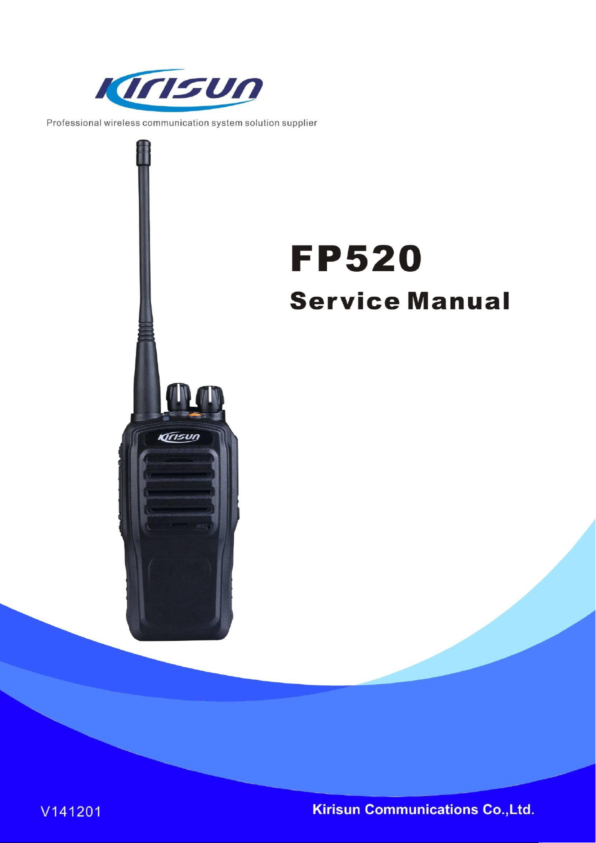
Chapter 2 External View and Functional Keys
2.1 External View
As figure 1 shows
FP520 Service Manual
Fig. 1
2.2 Functional Key Description
1. Side Button 1(Programmable Button)
2. PTT(PUSH-TO-TALK)Button
Press and hold the PTT button and talk to the microphone to transmit; release it to listen.
3. Side Button 2(Programmable Button)
4. Antenna
5. LED Indicator
The LED indicator lights up red when transmitting, and lights up green when receiving. In the condition of low
battery, the LED indicator flashes red.
6. Channel Knob
Rotate to select channel 1-16.
7. Emergency Button
8. On/Off/Volume Control Knob
Rotate clockwise to turn on the radio, and counter-clockwise until a click is heard to turn off.
When the radio is on, rotate to adjust the volume.
9. Speaker
10. Microphone
11. Speaker/ Microphone Interface
Open the cover to connect the radio with the external speaker and microphone.
Page 4 of 64
Page 6

FP520 Service Manual
Programmable Button
You can require the dealer to program the keys listed below as shortcuts to certain functions for your
convenience:
Long press key and short press key can be set: Side Button, Emergency Button.
Long press key can be set: menu key, cancel key.
Note:
Short Press: Press and release it quickly.
Long Press: Press and hold it down for 2 seconds, then release.
Available Functions:
None: No feature will be enabled.
Power Level Adjustment:Switch to high/low power.
Monitor:If there is CTCSS/CDCSS in the current analog channel, press the key and switch to squelch mode to
cancel the CTCSS/CDCSS feature. Press the key again to return to the original status.
Emergency Alarm On: Enable the emergency alarm feature to seek help.
Emergency Alarm Off: Disable the emergency alarm feature.
Squelch On/Off: Enable the squelch feature to receive the weak signal on the analog channel.
Squelch Level Adjustment: Adjust the signal strengthness the radio needs when receiving.
Scan: Receives the activity of other channels. Press to enable/disable the scan feature.
Whisper: Enable/disable the whisper feature. The receiver can hear clearly when you speak in a low voice with
this feature on.
2.3 LED Indicator
The LED lights up red when transmitting
The LED lights up green when receiving
The LED flashes red in the condition of low battery.
Page 5 of 64
Page 7
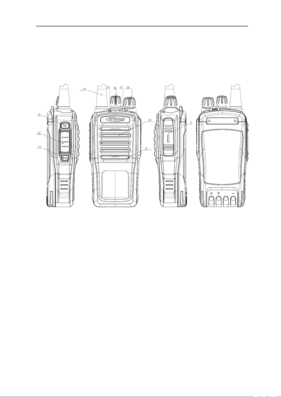
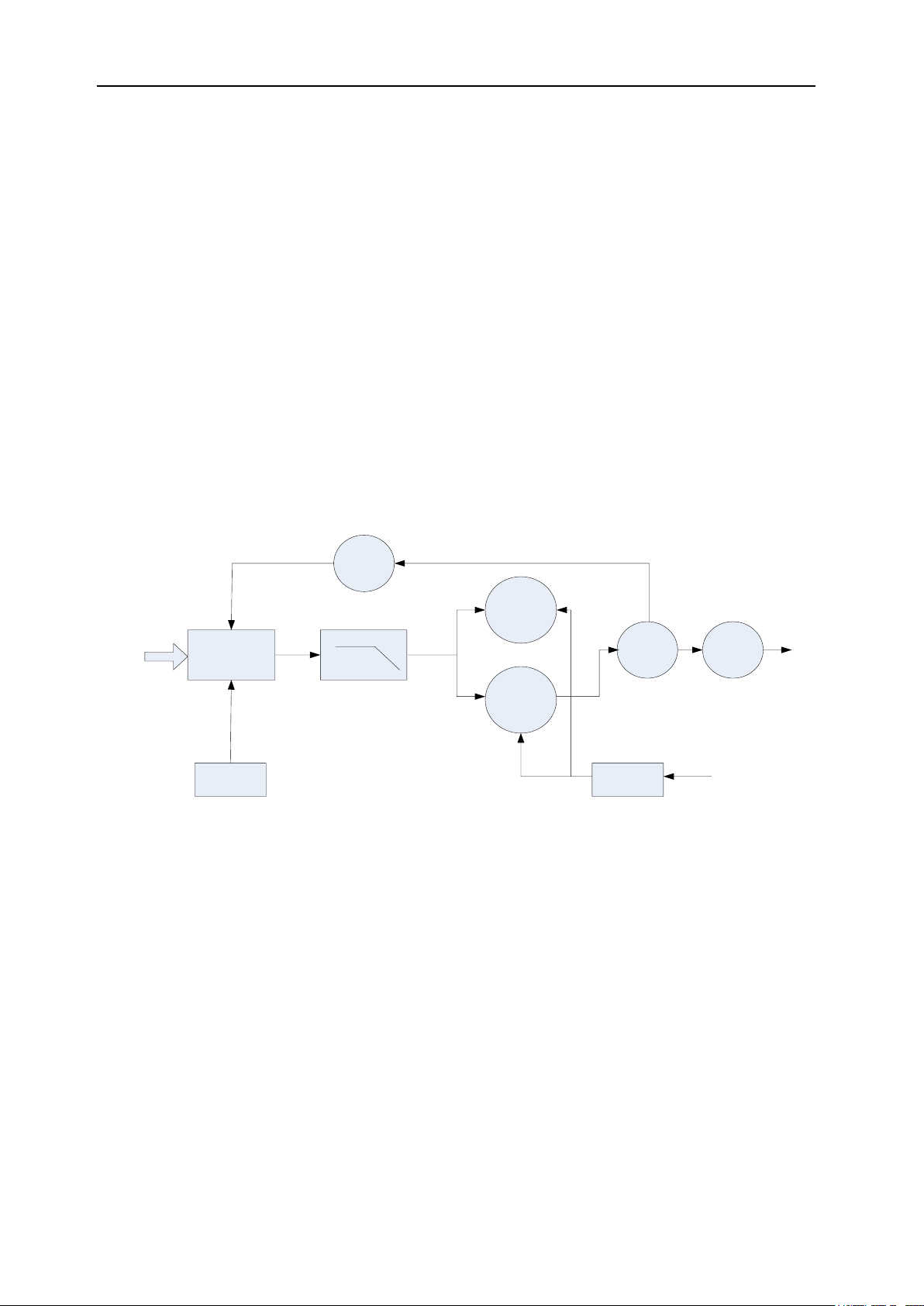
Chapter 3 Circuit Description
ANT SW
RF
AMP
PA
AMP
TX
AMP
PLL
VCO
IF SYSTEM
X4
multiply
TCXO12.8MHz
51.65MHz
MCF
CODEC
AF
AMP
MIC
CF
450KHz
ANT
MIXER
ANT SW
BPF
1st local
osc
BPF
MCF
IF AMP
Q701
IF DET
450K
CODECAF PA
SPK
D600 D601
D602 D603
MIXER
Q702
Z1
51.65MHz
U6U800
ANT
X4
Multiply
Q300
TCXO
MCU
IC2
PC/TV
Q703
RF AMP
CF1
3.1 Overview
This radio is FM portable equipment.
3.2 Frequency Configuration
FP520 Service Manual
Fig 3.1 Circuit Diagram
This Radio applies twice frequency mixing method. The first intermediate-frequency is 51.65MHz. The second
intermediate-frequency is 450 kHz.
The first local oscillation is generated by frequency synthesizer, and the second local oscillation is generated by the
quadruple frequency of 12.8MHz.
The transmitting signal is generated by frequency synthesizer.
The reference frequency of frequency synthesizer is generated by TCXO.
3.3 Principle of Receiver (RX)
Fig. 3.2 Principle of Receiver
Page 6 of 64
Page 8
FP520 Service Manual
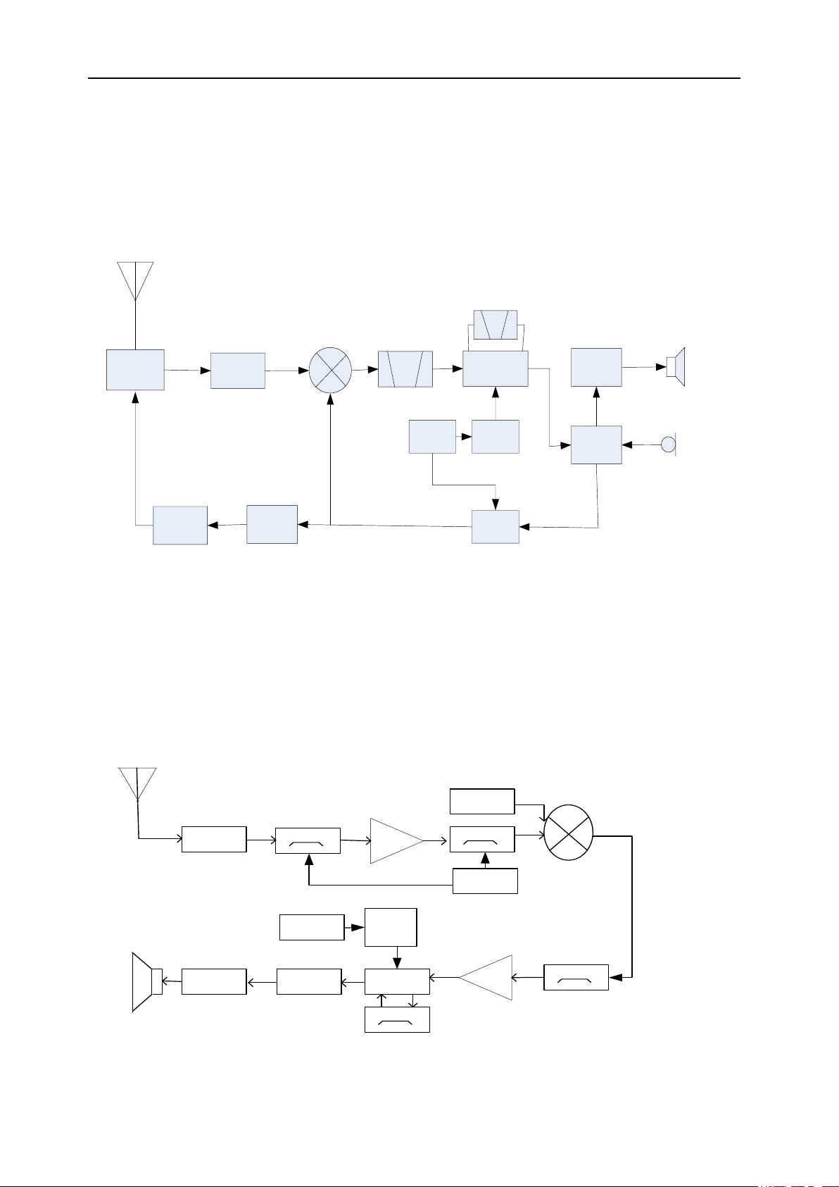
BT
SW
D402
AMP
Q602,Q603
DRIVE AMP
Q601
FINAL AMP
Q600
ANT SW
D600,D601
LPF
D602
RX
VCO
APC
IC600
DET
SW
Q604,Q605
APC
R620,R621,R622
ANT
5T
5T
Receiver Front End
Signals from the antenna through the receiving/transmission (RX/TX) switch (D600,D601,D602,D603), which
passed the band-pass filter (BPF) consisting of two levels of LC to eliminate the unnecessary signals, then sent to
the low noise amplifier (LNA) consisting of Q703 and its peripheral components for enlargement.
After passing the band-pass filter (BPF) consisting of three levels of LC to further eliminate the unnecessary
out-of-band signals, the output of LNA is then sent to the first frequency mixer (Q702).
The First Frequency Mixer
The signal from LNA is mixed with the first local oscillator signal from the frequency synthesizer to generate the first
intermediate-frequency signal (51.65MHz).
IF Circuit
The first intermediate-frequency signal eliminates the signals from the adjacent channels or other signals through
the crystal filter. (Z1)
The first intermediate-frequency signal from the crystal filter, being amplified by the first intermediate-frequency (IF)
amplifier (Q701), then sent to IF processing IC ( IC700,GT3136).
IF IC consists of the second frequency mixer, IF amplifier, amplitude limiter, frequency detector, noise amplifier,
audio low pass filter.
The 12.8MHz signal from X300, being amplified by Q300 and its peripheral circuit, becomes the second local
oscillation signal (51.2MHz). The second local oscillation signal (51.2MHz) mixes with the first
intermediate-frequency signal (51.65MHz) in IC700 to generate the second intermediate-frequency signal. The
second intermediate-frequency signal amplified in IC700 with its amplitude being limited, being filtered by the FD1
ceramic filter(450kHz), is demodulated by IC700 to generate the audio signal.
Squelch Circuit
The signal demodulated by IC700 is sent to its own noise amplifier for amplification, and the amplified signal is sent
to Q700 for further amplification and to D701 for detection; the produced direct current is then sent to MCU squelch
control circuit, and its voltage is inversely proportional to the input signal.
3.4 Principle of Transmitter (TX)
Page 7 of 64
Page 9
FP520 Service Manual
PLL
DATA
Q301
RF AMP
LPF
Q302
RX VCO
PLL
DATA
Q303
BUFF AMP
12.8MHz
TCXO
X300
IC300
PLL IC
Q307
TX VCO
Q305,Q306
SW
Q304
RF AMP
MCU
Fig.3.3 Diagram of Power Amplification and Antenna Switch Principle
The modulated RF signal from VCO, being amplified by Q303、Q304、Q602、Q603、Q601, is sent to Q600 for power
amplification.
The grid bias of Q601 and Q600 is controlled by APC (Automatic Power Control) circuit. Change the grid bias
voltage to easily control the output power strength of the transmitter.
APC(Automatic Power Control)Circuit
R620, R621 and R622 are power amplifier current detection, and IC600A is a power amplifier current sampling
amplifier. IC600B is a power comparison amplifier.
The extra high output power of the transmitter will increase the power amplifier current and IC600A output with a
decrease in IC600B output voltage. It will also decrease the bias voltage on Q601 and Q600, which decreases the
output power of the transmitter, and vice versa. This enables the stability of the output power in different working
circumstances.
MCU changes the voltage being sent to IC600B to set the power.
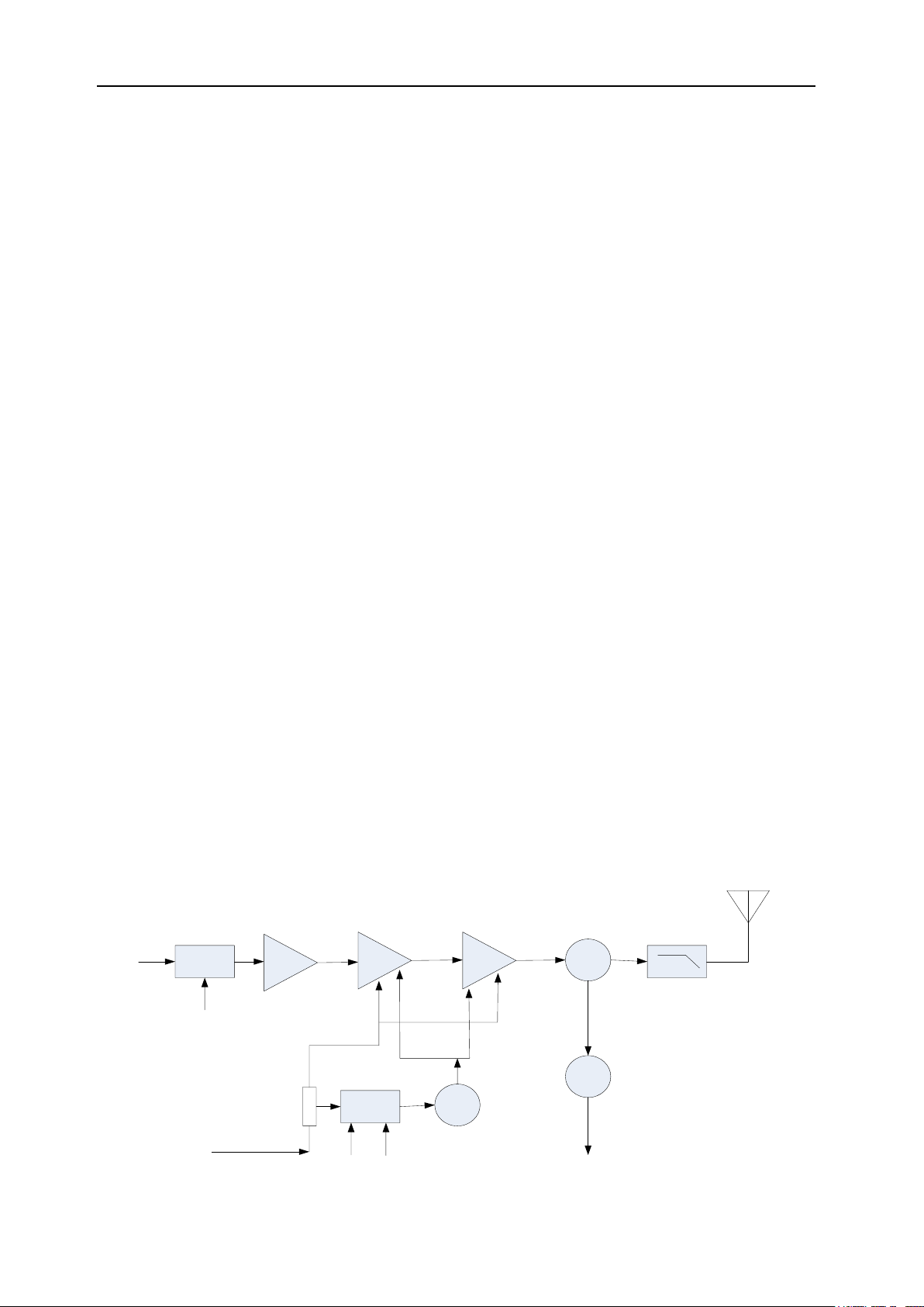
3.5 Principle of Frequency Synthesizer
Fig 3.4 Diagram of Frequency Synthesizer
This radio applies PLL frequency synthesizer.
The frequency synthesizer consists of reference oscillator, voltage controlled oscillator (VCO), programmable
frequency divider, phase comparator and low pass filter.
Q307, D305, D306, D307, D308 and other resistance-capacitance units make up the transmitting VCO unit. D304 is
the modulation circuit of the transmitting VCO.
Q302、D300、D301、D302、D303 and other resistance-capacitance units make up the receiving VCO unit.
IC300 (MB15E03) is a PLL integrated circuit which contains a programmable reference frequency divider,
programmable frequency divider, phase comparator and charge pump.
R329, C358, R330, C359, R331, R332 and C360 make up the loop filter.
The reference frequency is provided by X300 (TCXO,12.8MHz).
The reference frequency from TCXO (Temperature Controlled Crystal Oscillator)is divided by the programmable
reference frequency divider in IC300 to become the 5kHz or 6.25kHz (controlled by MCU, according to the setting
channel) reference frequency .
The oscillation frequency from VCO, being amplified by the two-time frequency multiplier circuit, is sent to IC300 for
Page 8 of 64
Page 10
FP520 Service Manual
FM receiver
FM modulatorPA
TR
SW
Host MCU
4FSK
Protocol
stack
Voice
coder
U6 CODECL
U6 CODECR
ANT
SCT3252
U1
IC2
SPK
MIC
comparison with reference frequency after being divided by the programmable frequency divider, and the error
signal is then generated to change the oscillation frequency of VCO after filtered by the low pass filter. VCO is
locked when the frequency of VCO reaches a certain set value.
Loss of Lock Detection: When PLL loses its lock, IC300 pin14 outputs the electric level signal to MCU, and MCU
control transmitter forbids transmitting and issues an alert tone. The output voltage of IC300 pin14 is high electric
level when it is locked.
3.6 Audio Processing Circuit
MIC Signal Processing:
The speech signal from MIC is sent to U6 for A/D switch, and sent to U1 SCT3252 for audio coding/decoding,
communication protocol processing, channel coding modulation. Afterwards, the signal outputs MOD2 and MOD1
separately from U6, and then sends them to TCXO and VCO for two-point modulation. The signal outputs 4FSK
modulating signal in digital state, and sine wave signal in analog state.
Receiving Audio Signal Processing:
The audio signal demodulated from IC700 is sent to U1 SCT3252 for processing after finishing A/D switch by U6.
After the audio encoding/decoding, communication protocol processing and DSP, the audio signal is sent to U6 for
D/A switch, and it is then output to the U800 (TDA2822) audio power amplifier for amplification so as to sound the
speaker.
Squelch Circuit:It is output from IC700 after demodulation, and it filters out the noise from the demodulated signal
after going through the filter circuit. It is sent to MCU after being detected by D701 and amplified by Q700. The MCU
identifies the noise level and controls the squelch.
Speaker Impedance: 16 Ω
Note: Any terminal of the speaker must not be attached to the ground!
The emergency alert tone is not controlled by volume.
3.7 Power Supply
This radio applies 7.4V battery. The transmitter power amplifier circuit (Q601, Q600) and receiver audio processor
(U800) directly use the battery for power supply with other circuits using the voltage stabilized 5V for power supply.
Q102:5T switch,controlled by MCU.
5T: Supplies power for the transmitter front end.
Q100: 5R switch,controlled by MCU.
5R: Supplies power for the receiver RF amplifier, frequency mixer, IF processor, audio signal processor and the like.
Page 9 of 64
Page 11

FP520 Service Manual
No.
Frequency [Hz]
No.
Frequency [Hz]
No.
Frequency [Hz]
No.
Frequency [Hz]
1
67.0
11
94.8
21
131.8
31
186.2
2
69.3
12
97.4
22
136.5
32
192.8
3
71.9
13
100.0
23
141.3
33
203.5
4
74.4
14
103.5
24
146.2
34
210.7
Q1:5C switch, controlled by MCU.
5C:The 5V power source controlled by power saving, and it supplies power for frequency synthesizer unit.
3.8 MCU Unit
MCU unit controls every unit operation of the radio to perform all the radio functions.
Communicates with the external PC
Deposits and withdraws the radio status data
Controls PLL to generates the local oscillation frequency of receiving and transmitting
Acquires the current channel status
Controls the LED status indication
Controls the power supply status of every unit
Detects the operation of every function key
Generates CTCSS signal
Generates DCS signal
Generates power-controlled signal
Completes CTCSS decoding
Completes DCS decoding
Squelch detection and control
Controls the content of voice prompt
Memorizer(E2PROM,AT24LC512BN)
It stores the radio channel data, CTCSS/DCS data, other function setting data and parameter adjustment data.
CTCSS/DCS Signal Encoding and Decoding:
The CTCSS/DCS signal generated by MCU is sent separately to VCO and TCXO for modulation.
The CTCSS/DCS signal from the receiver is sent to MCU for decoding. The MCU identifies whether the
CTCSS/DCS signal of the radio is the same as the receiving signal so as to turn on the speaker.
CTCSS
CTCSS(continuous tone control squelch system), a squelch control system modulated on the carrier with the
CTCSS signal being the pilot frequency. If the CTCSS feature is set, the conversation is enabled only when the
CTCSS frequency from the receiver and transmitter is the same to avoid interference from other signals.
39 groups of standard CTCSS frequency of this radio are available. See Chart 1.
CTCSS signal is generated by MCU (PWM wave form), and it is sent to VCO for modulation after being filtered by
the low pass filter composed of RC for eliminating the frequency higher than 300Hz.
Chart 3.1 CTCSS Frequency Chart
Page 10 of 64
Page 12
FP520 Service Manual
5
77.0
15
107.2
25
151.4
35
218.1
6
79.7
16
110.9
26
156.7
36
225.7
7
82.5
17
114.8
27
162.2
37
233.6
8
85.4
18
118.8
28
167.9
38
241.8
9
88.5
19
123.0
29
173.8
39
250.3
10
91.5
20
127.3
30
179.9
023
114
174
315
445
631
025
115
205
331
464
632
026
116
223
343
465
654
031
125
226
346
466
662
032
131
243
351
503
664
043
132
244
364
506
703
047
134
245
365
516
712
051
143
251
371
532
723
054
152
261
411
546
731
065
155
263
412
565
732
071
156
265
413
606
734
072
162
271
423
612
743
073
165
306
431
624
754
074
172
311
432
627
Pin No.
Port Name
Input/ output
Function
1
VCCN
D/A Output
TCXO tuned voltage output
2
TONE-OUT
D/A Output
TONE output
3
NC I NC
DCS Signaling:
DCS(Digital code squelch,), a continuous numerical code which is modulated along with the speech signal on the
carrier to control the squelch. If the DCS feature is set, the speaker is on only when the same DCS code is received
to avoid the unnecessary signal interference.
83 kinds of standard code of this radio are available. See chart 2.
DCS signal is generated by MCU (PWM wave form), and it is sent to VCO and TCXO for modulation after being
filtered by the low pass filter composed of RC for eliminating the frequency higher than 300Hz. VCO modulates the
high frequency of DCS signal and TCXO modulates the low frequency of DCS signal.
CTCSS/DCS signal from the receiver is sent to MCU for decoding. MCU identifies whether the receiving signal has
the same DCS code as the radio so as to turn on the speaker.
Chart 3.2 DCS Coding Chart
3.9 Semiconductor Device Description
MCU Description
Chart 3.3 Microprocessor (M30620) Port Description
Page 11 of 64
Page 13

FP520 Service Manual
4
EPDT
I/O
EEPROM data input/ output
5
EPCK
O
EEPROM clock
6
BYTE
I
Gnd 7 CNVSS
I
Gnd 8 BSHIFT
O
clock beat frequency control
9
SV O Min. volume control
10
RESET
I
CPU reset input
11
XOUT
O
CPU clock output
12
VSS
-
Gnd
13
XIN I CPU clock input
14
VCC
-
+5V
15
NC I +5V
16
PTT I PTT control pin input
17
EXT-PTT
I
External PTT control pin input
18
ENC_0
I
channel switch control pin input
19
ENC_1
I
channel switch control pin input
20
ENC_2
I
channel switch control pin input
21
ENC_3
I
channel switch control pin input
22
S_CS
I
data input pin(connects 3252)
23
S_SO
I
data input pin(connects 3252)
24
NC O NC
25
S_SCK
O
data input pin(connects 3252)
26
PC/TV
O
tuned voltage output pin
27
S_SI
I
3M
28
3M O 3M
29
TXD
O
TXD1 output
30
RXD
I
RXD1 input
31
C_CLK
O
JTAG test point
32
C_BUSY
O
JTAG test point
33
NC - NC
34
NC - NC
35
AFCO_1
O
RX control output pin
36
AFCO_2
O
RX control output pin
37
RX SW
O
Receiver VCO switch
38
TX SW
O
Transmitter VCO switch
39
C_EPN
I
JTAG test point
40
DT I PLL data pin
41
LE O PLL chip select pin
42
CK O PLL clock pin
43
UL O PLL losing lock detection pin
44
C_CE
I
JTAG test point
45
SCT3252MOD
O
data output pin(connects 3252)
46
GREEN_LED
I
green light control switch
Page 12 of 64
Page 14

FP520 Service Manual
47
RED_LED
I
red light control switch
48
5TC O 5T control pin
49
5RC
O
5R control pin
50
SAVE
I
5C control pin
51
INTO
O
data output pin(connects 3252)
52
PLLBYPASS
O
data output pin(connects 3252)
53
PLLSEL2
O
data output pin(connects 3252)
54
HCSN
O
data output pin(connects 3252)
55
HWRN
I
data input pin(connects 3252)
56
HRDN
O
data output pin(connects 3252)
57
HOBIB
O
data output pin(connects 3252)
58
RSTN_3252
O
data output pin(connects 3252)
59
NMI
O
data output pin(connects 3252)
60
ACC
-
3M
61
PIO3
O
data output pin(connects 3252)
62
VSS
-
Gnd
63
HPI_DATA0
I/O
HPI Data Bus(connects 3252)
64
HPI_DATA1
I/O
HPI Data Bus(connects 3252)
65
HPI_DATA2
I/O
HPI Data Bus(connects 3252)
66
HPI_DATA3
I/O
HPI Data Bus(connects 3252)
67
HPI_DATA4
I/O
HPI Data Bus(connects 3252)
68
HPI_DATA5
I/O
HPI Data Bus(connects 3252)
69
HPI_DATA6
I/O
HPI Data Bus(connects 3252)
70
HPI_DATA7
I/O
HPI Data Bus(connects 3252)
71
NC - NC
72
NC - NC
73
SI/D7
O
LCD control pin
74
SCL/D6
O
LCD control pin
75
AO O LCD control pin
76
/RST
O
LCD control pin
77
/CS1
O
LCD control pin
78
LAMP
O
backlight control pin
79
K0
O/I
digital key detection pin
80
K1
O/I
digital key detection pin
81
K2
O/I
digital key detection pin
82
K3
O/I
digital key detection pin
83
K4
O/I
digital key detection pin
84
K5
O/I
digital key detection pin
85
K6
O/I
digital key detection pin
86
K7
O/I
digital key detection pin
87
BATT
I
Voltage check input
88
RSSI
I
Receiving filed intensity signal input
89
BUSY
I
Squelch voltage check input
Page 13 of 64
Page 15
FP520 Service Manual
90
VOL_DET
I
digital potentiometer detection pin
91
NC - NC
92
GND
I
GND
93
PF I extension key detection pin
94
GND
-
Gnd
95
HEADPHONE_DET
I
NC
96
VREF
-
+5V
97
AVCC
-
+5V
98
GPS_C
O
GPS power control pin
99
BASSBAND_C
O
power time-delay control pin
100
BEEP_C
O
BEEP control pin
Position No.
Item No.
Function Description
U1
SCT3252
4FSK baseband processing chip
U6
WM8758B
stereophonic encoder-decoder
IC202
PST9140NR
MCU reset circuit
U300
MB15E03
frequency synthesizer
IC600
NJM2904
APC,voltage comparison, drive
IC700
GT3136
the second local oscillation, the second intermediate frequency
amplification, amplitude limiting, demodulation, noise amplification
IC204
NJM2902
demodulation signal amplification, filter
IC2
M30620
MCU
IC200
AT24C512C
E2PROM,stores channel frequency data, function setting parameter,
modulating status parameter
U800
TDA2822
receiver audio power amplification
Q302
2SK508NV
receiver VCO oscillator pipe
Q304
2SC5108
VCO buffer amplifier
Q305
DTA143TE
transmitter VCO control switch
Q301
2SC5108
feedback loop amplifier
Q306
DTA143TE
transmitter VCO control switch
Q308
2SC4617
VCO power filter
Q303
2SC5108
VCO buffer amplifier
Q300
2SC5108
receiver the second local oscillation amplifier
Q307
2SK508NV
transmitting VCO oscillator pipe
Q601
RD01MUS1
transmitter power amplifier drive
Q600
RD07S2B
transmitter the last stage power amplifier
Chart 3.4 Semiconductor Device Function Description
Page 14 of 64
Page 16
FP520 Service Manual
Q602
2SC5108
transmitter 1st amplification
Q603
2SC3356
transmitter 2rd amplification
Q604
DTA144EE
APC output switch
Q703
3SK318
receiver low noise amplifier
Q702
3SK318
the 1st level frequency mixer
Q701
2SC5108
the 1st intermediate frequency amplifier
Q700
2SC4617
receiver noise amplifier
Q800
FMMT717
audio output control switch
Q801
DTC144EE
audio power amplifier control switch
IC100
XC6204B502MR
adjustable 5C stable voltage output
IC100
XC6204B502MR
adjustable 5R stable voltage output
IC100
XC6204B502MR
adjustable 5T stable voltage output
IC102
XC6228D122VR
adjustable 1.8V voltage output
IC101
XC6204B332MR
adjustable 3V voltage output
Item
Item no.
Function Description
D309
DA2S10100L
losing lock detection diode
D310
DA2S10100L
VCO power filter accelerating diode
D304
1SV278
transmitter VCO modulation diode
D305,D306
D307,D308
HVC376
transmitter VCO oscillation variode
D300,D301
D302,D303
HVC376
receiver VCO oscillation variode
D402
HSC277
VCO output switch
D604
HZU5ALL
APC output voltage limiting diode
D600,D601
D602,D603
HVC131
transmitter antenna switch diode
D704,D705,D706,
D707,D708
HVC355B
receiver band pass filter and variode
D701
RB706F
communication diode
Chart 3.5 Diode Function Description
Page 15 of 64
Page 17

FP520 Service Manual
Chapter 4 Function Description and Parameter Settings
4.1 Time-out Timer
This feature prevents the user from long occupation of the channel. If the transmitting period exceeds the
dealer’s preprogrammed time, the radio stops transmitting and the rings alert tone. To stop the alert tone, please
release the PTT button. For a second transmission, please press the PTT button after a certain period (set by
the dealer). If the dealer preprograms the pre-warning feature, a warning is given when the transmitting period
gets close to its time-out-timer limitation, indicating the transmission is forbidden soon.
4.2 Channel Scan
The channel scan is able to search for the channel where there is a signal, and the radio stays on the channel
where a signal is detected for making a conversation. The scanning mode is the carrier control scan.
4.2.1 Carrier Control Scan
The radio scan stays on a busy channel until it is no longer busy, and the scan is enabled automatically after a
certain period (the specific period time is set by the local dealer).
Press the Scan shortcut key, and the radio scans the scan list of the current channel. When the radio is scanning,
you can press the “Scan” shortcut key to stop the scanning.
4.2.2 Scan Reply Channel
When the radio is scanning, press the PTT button to transmit and make a conversation on a preset channel, and
the channel is preprogrammed by the local dealer.
4.3 Kill and Activation
If the dealer preprograms this feature, the radio can receive and decode other radio’s signals of kill and
activation before responding accordingly. After being killed, the radio can only receive the activated signal
without being able to transmit or receive other signals. The radio is back to normal after activation.
4.4 Emergency
In a state of emergency, press the “Emergency On” shortcut key for the alarm call. The alarm method is
composed of two parts: Alarm type, which mainly specifies the acoustooptic reaction in the state of alarm call;
Alarm mode, which specifies the sending content in the state of alarm call. You can set these parameters
through the dealer to meet your requirements. To disable the emergency feature, please press the “Emergency
Off” shortcut key.
Alarm Type:
◆None: No alarm feature (by default), and the alarm feature cannot be enabled by pressing the emergency
button.
◆Siren Only: The radio only emits siren locally.
◆Regular: The acoustooptic alert can be enabled, and the radio is able to receive.
◆Secret: No acoustooptic alert and the radio is not able to receive.
◆Secret but receivable: No acoustooptic alert but the radio is able to receive.
Alarm Mode:
Page 16 of 64
Page 18
FP520 Service Manual
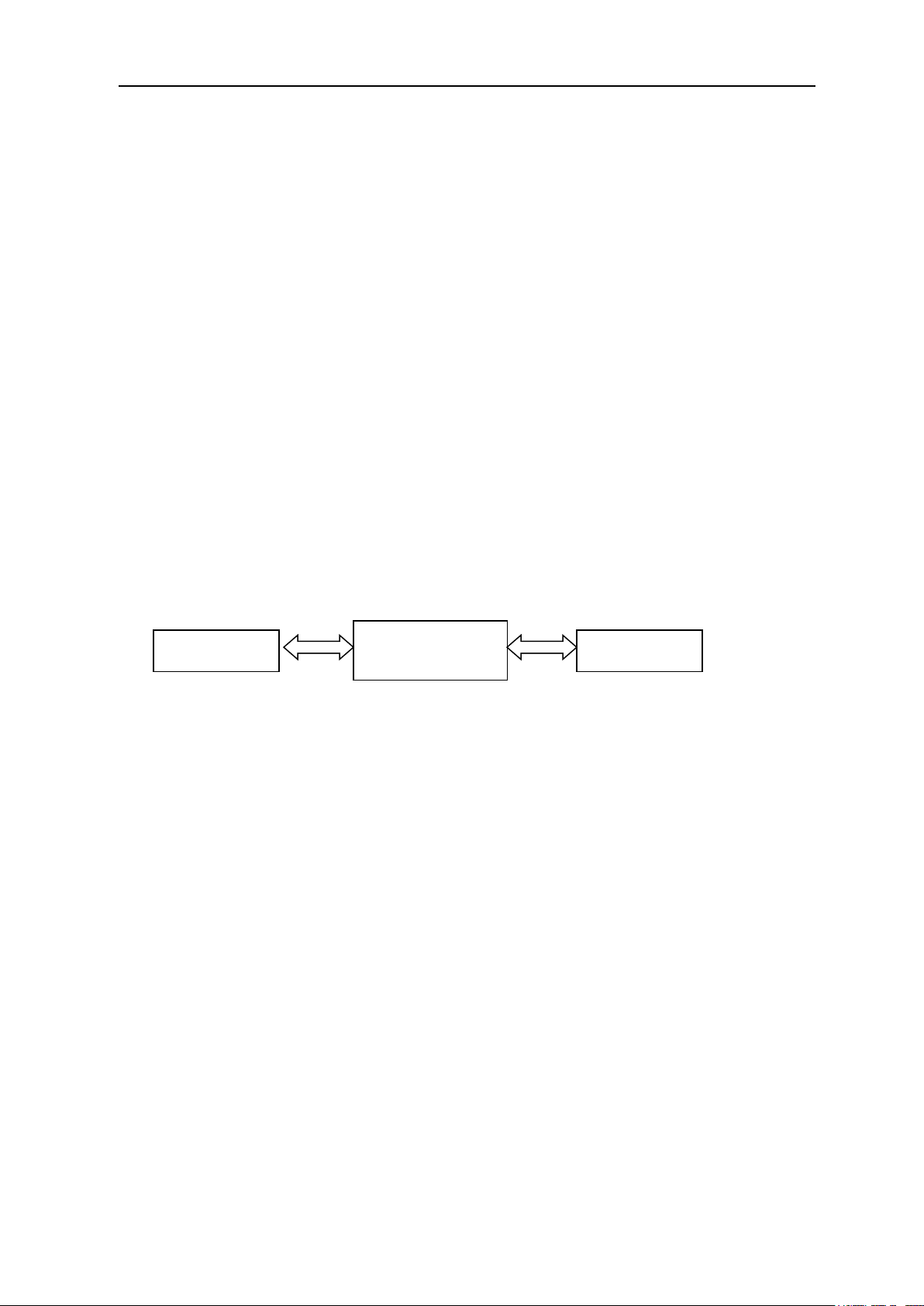
Computer
FP520
programming
Radio
◆Emergency Alarm: After the alarm feature is enabled, the radio only transmits an emergency alert, and
afterwards, then automatic exit the alarm status.
◆Emergency Alarm + Emergent Call: The radio transmits an emergency alarm and sends out an emergency
call by pressing the PTT button.
◆Emergency Alarm + Auto Transmission of Background Tone: The radio transmits an emergency alarm, and
the background tone will be sent out periodically and automatically in the way of emergency call.
Note:
Emergency Alarm:A non-speech signal transmitted by the radio to inform other radios to send out an alert.
Emergency Call:A call mode in the priority of using the channel to ensure a successful call during emergency.
4.5 Parameter Settings
The radio is preset before the factory delivery, but the parameter of the digital feature, operational frequency,
channel, QT/DQT, and auto scan feature may be reset according to different requirements of the customers.
Hence, Kirisun designed a Chinese/English FP520 programming software with friendly interface, easy operation
and clear visual display to complete the parameter settings for FP520.
The procedure of setting the parameter using a computer.
A. Install the FP520 programming software on the computer.
B. As Fig 4.5 shows, using the FP520 programming cable to connects the computer with the radio
Note: During the connection, ① make sure the computer is off.
② make sure the radio is off.
Fig 4.5
C.Turn on the computer.
D.Turn on the Radio.
E.Click the execution procedure, and operate FP520 programming software.
F.In the main menu of FP520 programming software, click “read” menu to input the radio parameter into the
computer.
G.For detailed operation, please refer to the “assistance” file of the programming software.
Page 17 of 64
Page 19

FP520 Service Manual
Chapter 5 Assembly and Disassembly
This radio is sophiscated communication equipment with a precise and compact mechanism. The assembly and
disassembly of the radio must be carefully done during the repair. The description is as follows:
5.1 Installing/Removing the Battery
Installing the Battery:
Press ① to bounce the belt clip; align the two bulges on the battery top with the corresponding slots on the
aluminum shell, and insert the battery into the aluminum shell in the direction as ② shows. Press the battery
bottom as ③ shows to completely bounce the latch, and the battery is attached until the battery is hooked as ④
shows (see Fig. 18).
Fig. 18
Removing the Battery:
Make sure the radio is off when removing the battery.
To remove the battery, please push the battery latch as ① shows to bounce the bottom of the battery as ②
shows, and take out the battery as ③ shows; if the belt clip is attached, please press it as ④ shows and remove
the battery downwards.
Fig 19
Notes::
Do not short circuit the battery terminals or abandon the battery into fire.
Do not take the risk of disassembling the battery shell.
Page 18 of 64
Page 20
FP520 Service Manual
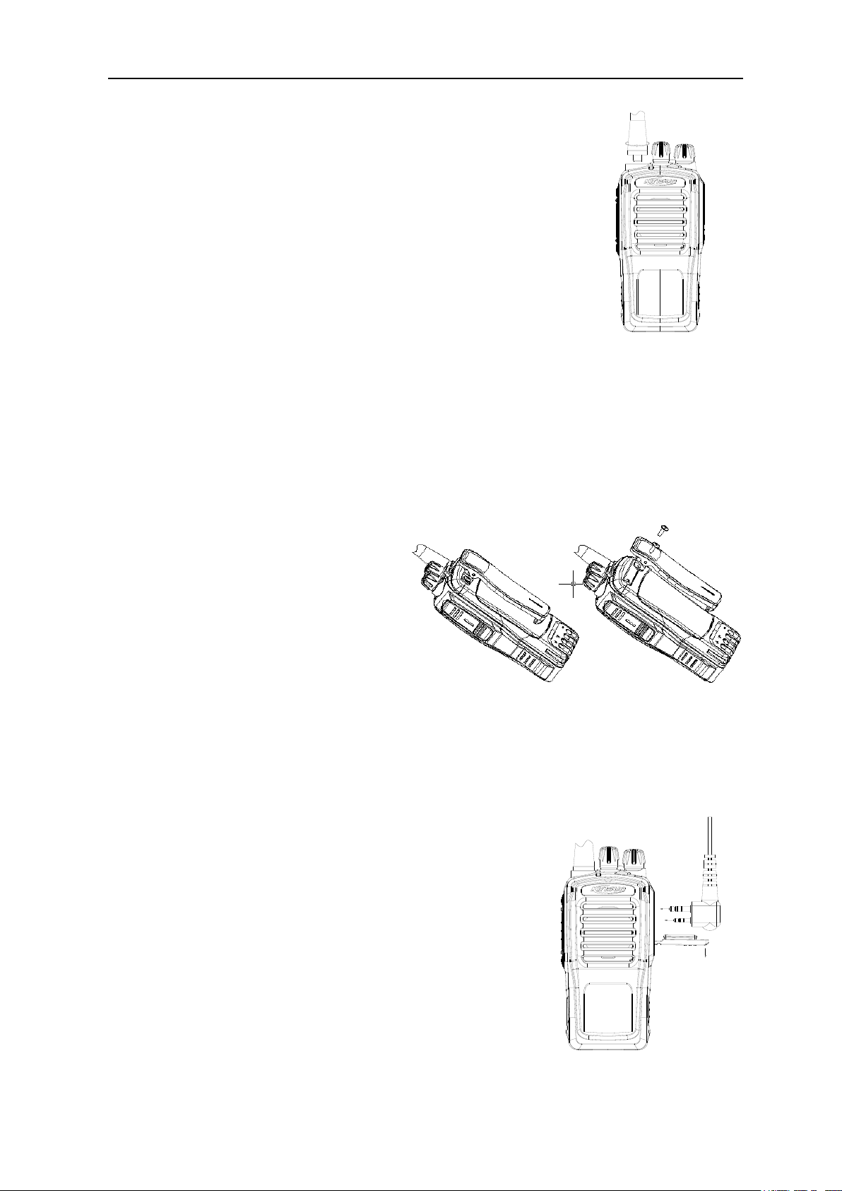
5.2 Installing/Removing the Antenna (see Fig. 20)
When installing, put the antenna end with screw thread into the threaded hole of the
radio top, and turn it clockwise until it is fastened.
For the removing, hold the antenna bottom and turn it counterclockwise.
Fig. 20
5.3 Installing/Removing the Belt Clip (see Fig.21)
When installing, align the screw holes of the belt clip with the corresponding ones of the radio back shell, and
use two 2.5x8.0 machine screws to fasten.
Loosen the two 2.5x8.0 machine screws to detach the belt clip.
Fig. 21
5.4 Installing the Earphone (see Fig. 22)
When the earphone is needed, open the earphone cover on the upper right
side of the radio, and put the earphone plug into the interface.
Fig. 22
Page 19 of 64
Page 21

FP520 Service Manual
5.5 Separating the Front Cover from the Chassis (see Fig. 23)
1. Removing the antenna, volume knob and channel knob;
2. Removing the two knob nuts and one antenna nut;
3. Removing the two aluminum screws with wabblers;
4. Use a pair of tweezers or other tools to lever open the bottom;
5. Pull out the Front Cover;
6. Use an electric soldering iron to cut off the speaker wire and MIC wire, and the separation is done.
Fig. 23
5.6 Separating the PCB Board from the Chassis (See Fig. 24)
1. Remove the potentiometer waterproof pad on top;
2. Remove the earphone waterproof plug;
3. Remove the screws on the PCB mainboard;
4. Remove the two screws on the side PTT PCB;
5. Use an electric soldering iron to cut off the antenna terminal and the PCB board is removed. (PTT PCB is
connected with the PCB mainboard. To avoid bonding pad damage, use an electric soldering iron to separate
them instead of dividing them with force)
Fig. 24
After the disassembly above is completed, the repair and adjustment can then be done.
5.7 Exploded View
Page 20 of 64
Page 22

FP520 Service Manual
No
.
Part no.
Description
Quantity
Remark
1
7SMF-020040M-SZYB-N
M2*4 round flat head
machine screw
13
fixes the PCB board, PTT button and
antenna screw
2
7MHP-4083-01A-W0
FP520 front cover
1
ABS+PC;black;silk screen/texturing
3
4SM7-6027-A40C
MIC microphone
1
Φ6.0, -40±2dB omnidirectional,2.2KΩ,2V,
with 80mm red black wire
4
7MHR-1727-09A-W3
microphone cover
1
Silica gel, hardness 40, orange
5
7MHP-7208-06A-W0
earphone cover plug
1
ABS+PC;black;texturing
6
7GCB-070001
microphone waterproof
cloth
1
waterproof cloth, diameterφ7mm,
thickness 0.1mm
7
7MHP-7208-07A-W0
earphone cover
1
TPU;black
8
7GCB-360001-W0
speaker waterproof net
1
Black, φ36
9
7PLJ-4083-E01A
LOGO sticker
1
T=0.3mm PC
10
4SS7-4050-016-100
speaker
1
MM4050-1638,16Ω,1W, ∅40
11
7MHR-7208-05A-W3
emergency button
1
silica gel; orange
Page 21 of 64
Page 23

FP520 Service Manual
12
7MHR-7208-04A-W9
light pipe
1
silica gel; transparent ; milk white
13
7MHR-7208-06A-W0
silica gel side button
1
silica gel; black
14
7MHP-7208-05A-W0
PTT cover
1
ABS+PC,black; texturing
15
7MHS-1140-01A-W
knob circlip
2
Material: spring steel
16
7MHP-7208-01A-W0
volume knob
1
ABS;black; white paint
17
7MHP-7208-02A-W0
channel knob
1
ABS;black; white paint
18
antenna
1
14mm diameter
19
7NRC-090136039-B1
antenna nut
1
yellow copper,inside diameter M9mm,
outside diameterφ13.6mm, 3.9mm
thickness, black passivation
20
7NRC-060100035-B1
switch nut
2
yellow copper, inside diameter M6mm,
outside diameterφ10mm,3.5mm
thickness, black passivation
21
7MHR-7208-02A-W0
top waterproof ring
1
silica gel; black
22
3CR7-SMA-50JFB-4
RF coaxial connector
1
SMA-J, attaching flange
23
7MHP-7208-04A-W0
earphone jack
waterproof plug
1
TPU; black
24
7MHR-7042-06B-W0
thermally conductive
silica gel gasket
1
silica gel, black,3*6*9mm
25
7SMF-020037M-SZCT-N
M2.0*3.7 cross
countersunk head
machine screw
2
fixes PTT PCB
26
7MHR-7208-01A-W0
radio big waterproof
rubber ring
1
silica gel; black; polishing
27
7MHR-4083-01A-W0
pedestal waterproof pad
silica gel, black, 60-degree hardness
28
7MHP-7208-03A-W0
main unit top cover
1
ABS,+PC black, texture
29
7MJS-7013-01B-N
KBJ-09 belt clip bracket
1
Stainless steel(SUS304), 1.00THK,bright
nickel plating
30
7MJS-7013-02A-W
KBJ-09 belt clip torsion
spring
1 31
7MJS-7013-03A-N
KBJ-09 belt clip rotation
shaft
1 32
7SMF-025080M-SZYB-Z1
M2.5*8 cross round flat
head machine screw
2
fixes the belt clip
33
7MJP-4026-01A-W0
KBJ-15 belt clip
1
DP770 belt clip,PC+ABS, black,
34
7MDP-7208-01A-W0A
battery top shell
1
ABS+PC; texturing
35
6PD7-7215-DPA
charging PCB
1
0.6MM thickness
36
6BLM-103445-074150-A
battery cell
1
Li-ion 1500mHA
37
7MDP-4083-03A-W0A
battery bottom cover
1
38
7SMF-020080M-MHHT-N1
M2*8 plum blossom
type thick head machine
screw
2
fixes the aluminum shell
39
7MHL-4083-01A-W
Aluminum shell
1
ADC12
Page 22 of 64
Page 24

FP520 Service Manual
40
7MHS-4083-01A-W
PTT button metal dome
1
φ6mm,SUS301 square metal dome
41
6PD7-4083-HPA
PTT PCB
1
42
6PM7-4085-HMB(VHF)
6PM7-4083-HMB(UHF)
main PCB
1
1.2mm thickness
43
7MHS-7042-01B-W
latch spring2
1
stainless steel (SUS301),0.25THK
44
7MHS-7042-01A-W
latch spring1
1
stainless steel(SUS301),0.25THK
45
7MHP-7042-14A-W0
battery latch
1
POM,black
46
7MHX-7042-02B-Z
battery hook 2
1
zinc alloy(Zn3#), eletrophoresis, black
47
7MHX-7042-02A-Z
battery hook 1
1
zinc alloy (Zn3#), electrophoresis, black
Model
Digital key 1
Digital key 2
Digital key 3
Digital key 4
Digital key 5
FP520 (VHF)
136.05MHz
145.55MHz
155.05MHz
164.55MHz
173.95MHz
FP520 (UHF)
400.05MHz
415.05MHz
435.05MHz
455.05MH
469.975MHz
Chapter 6 Adjustment
6.1 Method of Adjustment
During the service, a proper test and adjustment to the radio’s technical criteria is necessary after changing the
components.
6.1.1 Components Needed for the Adjustment
(1)antenna interface convertor
(2)universal interface
6.1.2 Manual Mode Adjustment
(1)The radio needs 5 frequency adjustment.
The frequency for the five digital keys is as follows:
6.1.3 Computer Adjustment Method:
A. VCO
The radio is receiving,
a) The channel is on the receiving high frequency, adjust C335 and test T300, the spot voltage is 3.6 ± 0.1V.
b) The channel is on the receiving low frequency, test T300, the spot voltage>0.6V
The radio is transmitting :
a) The channel is on the transmitting high frequency, adjust C371 test T300, spot voltage as 3.6±0.1V
d) The channel is on the transmitting low frequency, test T300, the spot voltage>0.6V
B. TX Part
1). Transmitting Frequency
Under the computer mode, the transmitting frequency is adjusted within ±100Hz.
2). Power
a. Under the computer mode (transmitting high power) (test in 5 frequency points), the transmitting high power is
adjusted to 3.8-4.2W.
b. Under the computer mode (transmitting low power) (test in 5 frequency points), the transmitting low power is
Page 23 of 64
Page 25

FP520 Service Manual
adjusted to 0.8-1.1W.
3). The Maximum Frequency Deviation (the modulation signal is 1kHz/120mV)
Under the computer mode [the maximum audio frequency deviation] (the broadband has five frequencies and
the narrowband has one; six frequencies in total), adjust the maximum transmitting frequency deviation to
1.8-2.5 kHz.
4). DTMF Frequency Deviation
Under the computer mode [DTMF frequency deviation] (six frequencies in total), adjust the DTMF frequency
deviation to 1.5-2 kHz.
5). DCS Balance
Under the computer mode, [DCS balance] (the broadband has five frequencies), adjust the DQT and make it
balanced, so the demodulated DQT wave can be square and smooth.
6). DCS Frequency Deviation(DQT:023N)
Under the computer mode, [DCS frequency deviation] (the broadband has five frequencies and the narrowband
has one; six frequencies in total), adjust DCS frequency to 0.3-0.5kHz.
7). CTCSS Frequency Deviation(QT:67.0Hz,150.4Hz,250.4Hz)
Under the computer mode, [CTCSS (67Hz, 150.4Hz,250.4Hz) frequency deviation] adjust the CTCSS
frequency deviation to 0.3-0.5kHz.
8). Battery low voltage indication when transmitting: the voltage is set as 6.8V,under the computer mode
[transmitting low voltage],click confirm when the digits are stabilized.
C. RX Part
1). Receiver Pass Band
a. Program the spectrum analyzer, and test the receiver pass band at the test point with a high frequency probe.
b. Under the computer mode [receiving sensitivity] (test in five frequency points), adjust the receiver pass band
to the corresponding center frequency.
2). The Maximum Volume
Set the RF frequency as the center frequency, the signal strength as 1mV, and the modulated frequency
deviation as 1.5 kHz. Under the computer mode, set the computer audio power as 1.1-1.3W.
3). Squelch
a. Set the RF signal as -121dBm and the modulated frequency deviation as 1.5 kHz. Under the computer mode
(on) (five frequency points), click confirm when the digits are stabilized.
b. Set the RF signal as -123dBm and the modulated frequency deviation as 1.5 kHz. Under the computer mode
(off) (five frequency points), click confirm when the digits are stabilized.
4). Field Strength
a. Set the RF signal as -121dBm and the modulated frequency deviation as 1.5 kHz. Under the computer mode
(low RSSI) (five frequency points), click confirm when the digits are stabilized.
b.Set the RF signal as -70dBm and the modulated frequency deviation as 1.5 kHz. Under the computer mode
(high RSSI) (five frequency points), click confirm when the digits are stabilized.
6.2 Radio Test
The following criteria should be tested:
A. Receiving part
1). Sensitivity: <= -119dBm (0.25uV) (broad band, narrow band) 12dB SINAD
2). Distorsion: <=5%
3). Current: static current: <=100mA
Page 24 of 64
Page 26

FP520 Service Manual
Model
FP520
Frequency
(400 ~ 470) MHz
(136 ~ 174) MHz
Modulation Method
4FSK
Channel Capacity
32 (two zones)
Channel Spacing
12.5kHz
Intermediate Frequency
The first intermediate frequency:51.65MHz; the second intermediate frequency:
Voltage
7.5V negative pole is connected to the ground
Temperature
-25℃~ +55℃
Antenna Impedance
50Ω
Microphone Impedance
2.2kΩ
Battery (Standard)
Li-ion battery DC 7.4V , 1500mAh,duration:12.5 hours
Dimension
118.2mm x55.7mmx32.9mm (width×height×thickness)
Weight
250(with battery and antenna)
Receiving working current: <=400mA
4). QT/DQT decode: <= -116dBm (0.35uV) (broad band, narrow band) the radio could decode correctly.
5).Sensitivity of squelch-off:the RF input ≤ -124dBm,the squelch feature should be disabled.
6). Sensitivity of squelch-on: the RF input ≥- 119dBm,the squelch feature should be enabled.
B. Transmitting part
1). Output power:High (3.5W---8W); low (0.3W---0.7W)
2). Transmitting current: High power transmitting <= 1.6A; low power transmitting <=1.0A
3). The maximum frequency deviation:3.8 kHz---4.8 kHz (broad band)
1.8 kHz---2.5 kHz (narrow band)
4). Distortion of transmitting :<=5%
5). QT/DQT frequency deviation :0.5---0.85 kHz (broad band); 0.3---0.5kHz(narrow band); with a good wave.
6). Transmitting frequency deviation:nominal frequency +/-500Hz
7). DTMF frequency deviation: 3~4kHz (broad band)/1.5~2.0 kHz(narrow band)
8). FFSK frequency deviation: 3~4kHz (broad band)/1.5~2.0 kHz(narrow band)
9). Under voltage indication:The voltage is set as 6.6V, and the red light flashes without the transmitting power
when press the PTT button.
Chapter 7 Major Specifications
7.1 General Specification
Page 25 of 64
Page 27

FP520 Service Manual
7.2 RX Part
Sensitivity (12dB SINAD)
≤0.25μV
Squelch-On Sensitivity
≤0.18uV
Receiver Residual Output
≤-35dB
Modulation Receiving Bandwidth
±3.5kHz
Adjacent Channel Selectivity
≥50dB
Intermodulation Interference Rejection
≥65dB
Spurious Response Rejection
≥70dB
Audio Output Power
1.3W,BTL @Distortion≤10%,16Ω
Receiving Consumption Current
≤400mA
7.3 TX Part
Tx Power
4.0W/1.0W @ 7.5V DC
Frequency Stability
≤ ±2.5ppm
The Maximum Modulation Frequency Deviation
±2.5kHz
Modulation Distortion(300~3000Hz)
≤ 3%
Adjacent Channel Transmitting Power
≥60dB
Spurious Transmitting
≥70 dB
Residual Modulation Frequency
≥40 dB
Transmitting Consumption Current
≤1.7A @ 7.5V DC
Page 26 of 64
Page 28

FP520 Service Manual
No.
Equipment
Specification
1.
Standard Signal
Generator
Frequency Range: 136-174MHz, 400-470MHz
Modulation: FM and External Modulation
Output: -127dBm/0.1uv or ≥-47dBm/1mv
2.
Power Meter
Input Impedance: 50Ω
Operation Frequency: 136-174MHz and 400-470MHz
Measurement Range: About 10W
3.
Deviation Meter
Frequency Range: 136-174MHz, 400-470MHz
4.
Digital Voltmeter
Measurement Range: DC 10mv-10v
Input Impedance: high input impedance for the minimum circuit
5.
Oscilloscope
Frequency Range: DC to 30MHz
6.
High Sensitivity
Frequency
Counter
Frequency Range: 50Hz to 10KHz
Frequency Stability: 0.2ppm or lower
7.
Ammeter
Maximum Current: 5A
8.
Audio Frequency
Voltmeter
Frequency Range: 50Hz to 10KHz
Volt Range: 1mv to 10v
9.
Audio Frequency
Generator
Frequency Range: 50Hz to 5KHz or higher
Output: 0Vto 1V
10.
Spectrum
Measurement Range: DC - 1GHz or higher
11.
Path Generator
Center Frequency: 50KHz to 600MHz
Output Voltage: 100mv or higher
12.
16Ω Dummy Load
About 16Ω,3W
13.
Adjustable Power Supply
5v to 10v,about 5A
Chapter 8 Service and Test Equipment
During the service and test, the following equipment and apparatus are needed.
Page 27 of 64
Page 29

FP520 Service Manual
Chapter 9 KBC-51 Charger
9.1 The Operational Conditions and Basic Specification of Charger
a) Battery Specification:Li-ion(2*3.7V), Ni-MH (6*1.2V),battery capacity (1~2.4AH).
b)Power Adaptor Specification: DC 11V~16V,500~1500mA power adaptor,standard voltage is 12V.
c) No-load Input Current:≤ 15mA
d) Precharged Current:75 mA±10 mA
e) Precharged Time Limit:15Min
f) Constant Current Charging Current:400 mA±40 mA
g) Maximum Li-ion Charging Voltage:8.32~8.42V;Maximum Ni-MH Charging Voltage: 9.6±0.1V
9.2 Function Introduction
1. This charger is intelligent with fast charging, reliability, safety and high charging saturation.
2. Status Indication: The indicator flashes red for precharging and lights red for charging; it lights green for
full charging, no battery and battery protection; it flashes yellow for battery output short circuit.
3. The external port identifies the lithium battery and Ni-MH battery.
4. Battery Short Circuit Protection: When there is a short circuit in the negative and positive pole of the charger,
the indicator flashes yellow and the charging current will be cut off. The charging will continue automatically after
troubleshooting.
5. The full battery is recharged for identification: When the full NI-MH battery is recharged, it will continue the
charging. The charger according the normal –ΔV to identify if the battery is full charged. When the full Li battery
is recharged, if the voltage is higher than 8.25V, the charging stops, and if it is lower than 8.25V, the charging
continues.
6. Temperature Protection: When the Li-ion battery is charging, the charging stops with the yellow light on if the
temperature is higher than 55 degrees. The charging is restarted when the temperature is down to 45 degrees.
When the Ni-MH battery is charging, the charging stops with the yellow light on if the temperature is higher than
60 degrees. The charging is restarted when the temperature is down to 50 degrees.
7. Put the radio on the charger when it is on standby mode, and the charging automatically begins when the
battery voltage is lower than 8.2 V.
8. The yellow light indicates the charger automatic protection. The charging is restarted after the
troubleshooting.
LED lights red: Charging
LED lights green: Full battery
LED lights yellow: Abnormal charging
Page 28 of 64
Page 30

FP520 Service Manual
No.
Problems
Causes and Solutions
1
Power-on Failure
A.The battery pack may be out of power. Please charge it or
change to a new one, then try again.
B.The power switch failure. Change to a new power switch.
C.CPU failure. Change to a new CPU.
D.Protective tube F100 failure. Change to a new protective tube.
2
PLL is unlocked
(beeping)
A.The PLL crystal oscillator is broken, please change to a new one.
B.The oscillation tube is broken, please change to a new one.
C.The PLL chip IC300 is broken,please change to a new one.
3
Communication Failure
A.The frequency is not the same. Please reselect a channel with
the same frequency
B.The signaling codes of CTCSS/DCS are different,please reset
them with the computer.
C.Beyond the communication range.
4
No Signal
A.The antenna is in poor contact,please fasten it again.
B.Low sensitivity,adjust the parameter in the “test mode”.
C.The high-mu tube Q703 is broken, please change it.
D.The squelch level is too high to turn it on, please adjust the
squelch level.
E.Mixer tube Q702 is broken, please change it.
F.FM processing chip IC700 is broken, pleas change to a new IC.
5
No voice on the
receiving radio when the
indicator glows red on
the transmitting radio.
A.The power amplifying tube is broken with no power output,
please change it.
B.The microphone is broken, please change it.
C.The operational amplifier Q601 is broken, please change it.
6
No voice received when
the indicator glows
green.
A.The speaker is broken, please change it.
B.The audio power amplifier U800 is broken, please change to a
new IC.
C.The switch diode Q801is broken, please change it.
7
Abnormal Programming
A.Improper connection, please check the cable connection.
B.The computer serial port output is abnormal, please check the
computer.
C.The earphone jack is in poor contact, please check it and change
it if broken.
Chapter 10 Troubleshooting
Page 29 of 64
Page 31

FP520 Service Manual
Appendix 1 Abbreviation
AMP Amplify, Amplifier
ANT Antenna
APC Automatic Power Control
BPF Band Pass Filter
CTCSS Continuous Tone Control Squelch System
DCS Digital Code Squelch
DEMOD Demodulation
E2PROM Electrically Erasable Programmable Read-Only Memory
HPF High Pass Filter)
IDC Instantaneous Deviation Control
IF Intermediate Frequency
LED Light-Emitting Diode
LNA Low Noise Amplifier
LPF Low Pass Filter
MCU Micro Control Unit
MIC Microphone
MOD Modulation
MONI Monitor
PLL Phase-Lock Loop
PTT Push-To-Talk
RX Receiver
SPK Speaker
TCXO Temperature Control Oscillator
TX Transmitter
UL Un-Lock
VCO Voltage Control Oscillator
Page 30 of 64
Page 32

FP520 Service Manual
Part No.
Item Name.
Specification
Quantit
y
Plug-in Position
6PM7-4083-HMB
FP520 PCB Board
FP520U-MAIN-140106.PCB;1.0MM;47X101.5MM; FR-4, four layers,
Pb-free
1
Mainboard PCB
1DS1-HSC277
Chip switch diode
HSC277,1608
3
D402, D602, D700
1DS1-HVC131
Chip switch diode
HVC131(P1),1608
2
D600, D601
1DS1-DA2S10100L
Chip switch diode
DA2S10100L
3
D309, D310, D709
1DS1-RB706F-40
Chip switch diode
schottky diode
RB706F-40,SOT-323
1
D701
1DV1-1SV278
chip varactor
1SV278(T1)
1
D304
1DV1-HVC376B
chip varactor
HVC376B(B9)
13
D300, D301, D302, D303, D305, D306, D307, D308, D704, D705, D706, D707, D708
1DZ1-HZU5ALL
Chip voltage stabilizing diode
HZU5ALL,2012,5V
1
D604
1IL1-NJM2904V
chip linear IC
Dual operation amplifier NJM2904V,TSSOP-8
1
IC600
1IM1-AT24C512C
Chip memorizer IC
(1IM1-AT24C512BN replaceable)
AT24C512C,manufaturer: ATMEL, Pb-free
1
IC200
1IS1-MB15E03SL
chip PLL IC
MB15E03SL,TSSOP-16
1
IC300
1IS1-PST9124NR
chip reset IC
reset IC,PST9124NR
1
IC202
1IS1-SCT3252PS
digital baseband processing chip
SCT3252PS,LQFP100,Nantong vocoder,Pb-free
1
U1
1IS1-GT3136
chip special IC
GT3136,SSOP16
1
IC700
1IS1-TDA2822
chip special IC
TDA2822
1
U800
1IS1-WM8758B
CODEC chip
WM8758CB, 32-Pin QPN encapsulation 5*5*0.9MM, Pb-free
1
U6
1IS1-XC6204B502MR
chip voltage stabilization IC
voltage stabilization IC 5V, SOT-23-5
1
IC100
1TF1-2SK1824
chip FET
2SK1824(B1)
3
Q606, Q6, Q704
1TF1-2SK508NV-K52
chip FET
2 Q302, Q307
1TF1-3SK318
chip dual-gate FET
3SK318(YB-)
2
Q702, Q703
1TF1-RD01MUS2
chip FET
1 Q601
1TF1-RD07MUS2B
chip FET
Mitsubishi,RD07MUS2B,Pb-free
1
Q600
1TF1-ST2302
chip FET
ST2302,SOT-23
2
Q802, Q803
1TT1-2SA1586
chip triode
2SA1586
1
Q805
1TT1-2SC3356-R24
chip triode
2SC3356-R24,SOT23,NPN
1
Q603
1TT1-2SC4617-R
chip triode
2SC4617-R(BR),EMT3
2
Q308, Q700
1TT1-2SC5108-Y
chip triode
2SC5108-Y(MC),NPN
6
Q300, Q301, Q303, Q304, Q602, Q701
1TT1-DTA143TE
chip triode
Digital diode DTA143TE(93), SOT323
3
Q305, Q306, Q604
1TT1-DTC144EE
chip triode
Digital diode DTC144EE(26), SOT323
11
Q2, Q4, Q101, Q103, Q200, Q201, Q605, Q801, Q804, Q806, Q707
1TT1-FMMT717TA
chip triode
FMMT717A,PNP,SOT23
1
Q800
1TT1-KTA1298-Y
chip triode
KTA1298-Y,SOT23
4
Q1, Q3, Q100, Q102
2CA1-TZVY2Z100A110
chip Trimmer capacitance
2-10P,+100/-0%,NP0±300PPm/℃
2
C335, C371
2CC1-10-C0G500-100D
Chip multilayer capacitance
1005,10P±0.5P,50V,C0G
4
C308, C309, C318, C321
2CC1-10-C0G500-101J
Chip multilayer capacitance
1005,100P±5%,50V,C0G
6
C329, C361, C375, C621, C643, C765
Appendix 2 Spare Part List (Electronic Part 400-470MHz)
Page 31 of 64
Page 33

FP520 Service Manual
2CC1-10-C0G500-120J
Chip multilayer capacitance
1005,12P±5%,50V,C0G
2
C331, C363
2CC1-10-C0G500-150J
Chip multilayer capacitance
1005,15P±5%,50V,C0G
1
C327
2CC1-10-C0G500-160J
Chip multilayer capacitance
1005,16P±5%,50V,C0G
1
C311
2CC1-10-C0G500-180J
Chip multilayer capacitance
1005,18P±5%,50V,C0G
2
C620, C732
2CC1-10-C0G500-220J
Chip multilayer capacitance
1005,22P±5%,50V,C0G
3
C225, C227, C618
2CC1-10-C0G500-270J
Chip multilayer capacitance
1005,27P±5%,50V,C0G
1
C313
2CC1-10-C0G500-2R0C
Chip multilayer capacitance
1005,2P±0.25P,50V,C0G
2
C302,C731
2CC1-10-C0G500-330J
Chip multilayer capacitance
1005,33P±5%,50V,C0G
2
C754,C355
2CC1-10-C0G500-3R0C
Chip multilayer capacitance
1005,3P±0.25P,50V,C0G
6
C702, C328, C305, C741, C725, C724
2CC1-10-C0G500-470J
Chip multilayer capacitance
1005,47P±5%,50V,C0G
1
C306
2CC1-10-C0G500-4R0C
Chip multilayer capacitance
1005,4P±0.25P,50V,C0G
3
C324, C332, C364
2CC1-10-C0G500-5R0C
Chip multilayer capacitance
1005,5P±0.25P,50V,C0G
5
C314, C315, C356, C703, C704
2CC1-10-C0G500-680J
Chip multilayer capacitance
1005,68P±5%,50V,C0G
1
C323
2CC1-10-C0G500-6R0C
Chip multilayer capacitance
1005,6P±0.25P,50V,C0G
4
C723, C700,C736,C333
2CC1-10-C0G500-820J
Chip multilayer capacitance
1005,82P±5%,50V,C0G
1
C759
2CC1-10-C0G500-R50B
Chip multilayer capacitance
1005,0.5P±0.1P,50V,C0G
4
C343, C362, C325, C357
2CC1-10-X5R6R3-105K
Chip multilayer capacitance
1005,1uF±10%,6.3V,X5R
6
C81, C6, C60, C61, R807, C38
2CC1-10-X7R160-104K
Chip multilayer capacitance
1005,100nF±10%,16V,X7R
38
C40, C10, C12, C14, C21, C22, C23, C24, C25, C26, C27, C28, C32, C39, C50, C51, C55, C56, C89, C91, C92, C100,
C101, C111, C114, C224, C334, C345,C707, C715, C749, C764, C801, C808, C816, C818, C819, C822
2CC1-10-X7R500-333K
Chip multilayer capacitance
1005,33nF±10%,25V,X7R,2CC1-10-X7R250-333K 代用
2
C48, C57
2CC1-10-X7R500-102K
Chip multilayer capacitance
1005,1000P±10%,50V,X7R
24
C34, C122, C304, C322, C347, C351, C366, C612, C636, C645, C647, C706, C709, C711, C712, C713, C714, C742,
C743, C751, C753, C72, C54, C41
2CC1-10-X7R500-103K
Chip multilayer capacitance
1005,10nF±10%,50V,X7R
15
C46, C47, C720, C719, C5, C341, C112, C115, C629, C639, C640, C648, C726, C800, C812
2CC1-10-X7R500-182K
Chip multilayer capacitance
1005,1800P±10%,50V,X7R
2
C708, C820
2CC1-10-X7R500-471K
Chip multilayer capacitance
1005,470P±10%,50V,X7R
81
C42, C43, C45, C58, C59, C102, C104, C105, C107, C108, C110, C113, C207, C208, C221, C222, C230, C231, C232,
C233, C300, C301, C307, C316, C320, C336, C337, C338, C339, C53, C52, C755, C756, C757, C758, C760, C762,
C763, C803, C804, C809, C810, C813, C814, C821
2CC1-16-C0G500-120J
Chip multilayer capacitance
1608,12P±5%,50V,C0G
1
C607
2CC1-16-C0G500-1R0C
Chip multilayer capacitance
1608,1P±0.25P,50V,C0G
1
C634
2CC1-16-C0G500-1R5C
Chip multilayer capacitance
1608,1.5P±0.25P,50V,C0G
1
C604
2CC1-16-C0G500-220J
Chip multilayer capacitance
1608,22P±5%,50V,C0G
1
C602
2CC1-16-C0G500-270J
Chip multilayer capacitance
1608,27P±5%,50V,C0G
1
C610
2CC1-16-C0G500-2R0C
Chip multilayer capacitance
1608,2P±0.25P,50V,C0G
2
C603, C614
2CC1-16-C0G500-330J
Chip multilayer capacitance
1608,33P±5%,50V,C0G
1
C326
2CC1-16-C0G500-3R5C
Chip multilayer capacitance
1608,3.5P/3.6±0.25P,50V,C0G
1
C605
2CC1-16-C0G500-4R0C
Chip multilayer capacitance
1608,4P±0.25P,50V,C0G
1
C616
2CC1-16-C0G500-5R0C
Chip multilayer capacitance
1608,5P±0.25P,50V,C0G
4
C365, C601, C613, C615
Page 32 of 64
Page 34

FP520 Service Manual
2CC1-16-C0G500-6R0C
Chip multilayer capacitance
1608,6P±0.25P ,50V,C0G
1
C608
2CC1-16-C0G500-6R0D
Chip multilayer capacitance
1608,6P±0.5P,50V,C0G
1
C609
2CC1-16-X7R500-471K
Chip multilayer capacitance
1608,470P±10%,50V,X7R
1
C611
2CC1-20-Y5V160-106Z
chip multilayer capacitance
2012,10uF+80%/-20%,16V,Y5V
24
C8, C9, C11, C15, C16, C17, C18, C63, C103, C106, C109, C116, C119, C319, C344, C348, C642, C750, C752, C802,
C806, C815, C817, C49
2CT1-TS32-160-1R0M
chip tantalum capacitance
3216,1μF±20%,16V,TS series (A level)
1
C359
2CT1-TS32-350-R10M
chip tantalum capacitance
3216,0.1μF±20%,35V, TS series (A level)
1
C358
2CT1-TS32-6R3-150M
chip tantalum capacitance
3216,15μF±20%,6.3V,TS TS series (A level)
2
C1, C376
2CT1-TS35-6R3-101M
chip tantalum capacitance
C-TAN,100uF,20%,SIZE-B,6.3V
1
C805
2LH1-R401R5-R03-05
chip air core inductance
wire diameter φ0.40,inner diameter φ1.5,3 circles, pin height 0.5mm,
clockwise circling
8
L600, L601, L603, L709, L710, L711, L713, L714
2LH1-R401R5-R04-05
chip air core inductance
wire diameter φ0.40, inner diameter φ1.5,4 circles, pin height
0.5mm,clockwise circling
2
L602, L605
2LH1-R401R5-R08-05
chip air core inductance
wire diameter φ0.40, inner diameter φ1.5,8 circles, high pin
1
L607
2LH1-R501R5-L05-05
chip air core inductance
wire diameter φ0.50, inner diameter φ1.5,5 circles, high pin
1
L606
2LL1-16-12NJ
laminated inductance
1608,12nH±5%(MLG1608B12NJ/LL1608-FH12N)
1
L611
2LL1-16-1R0K
laminated inductance
1608,1μH±10%(MLF1608A1R0K)
1
L703
2LL1-16-22NJ
laminated inductance
1608,22nH±5%(MLG1608B22NJ)
1
L311
2LL1-16-27NJ
laminated inductance
1608,27nH±5%(MLG1608B27NJ)
1
L609
2LL1-16-33NJ
laminated inductance
1608,33nH±5%(MLG1608B33NJ)
1
L313
2LL1-16-3N9S
laminated inductance
1608,3.9nH±0.3nH(MLG1608B3N9S)
1
L604
2LL1-16-3R3K
laminated inductance
1608,3.3μH±10%(MLF1608A3R3K TA00)
2
L309, L323
2LL1-16-82NJ
laminated inductance
1608,82nH±5%(MLG1608B82NJ)
2
L307, L310
2LL1-16-R22J
laminated inductance
1608,0.22μH±5%(LG HK 1608R22J-T/MLG1608B220N)
4
L306, L319, L324,,L303
2LL1-16-R56K
laminated inductance
1608,560nH±10%(MLF1608DR56K)
1
L300
2LW1-16UC-180J
chip wire wound inductance
1608,18nH±5%,ceramic core (C1608CB-18NJ)
3
L301, L700, L304
2LW1-16UC-181J
chip wind wound inductance
1608,180nH±5%, ceramic core (C1608CB-R18J)
1
L321
2LW1-16UC-680J
chip wind wound inductance
1608,68nH±5%, ceramic core (C1608CB-68NJ)
2
L701, L706
2LW1-20UC-221J
chip wind wound inductance
2012,220nH±5%, ceramic core (LQN21AR22J/LQW2BHNR22J03L)
1
L608
2LW1-25UC-103J
chip wind wound inductance
2520,10μH±5%, ceramic core (FLM2520-100J)
1
L305
2LW1-25UC-331K
chip wind wound inductance
2520,330nH±10%, ceramic core (FLM2520-R33K/SGWI2520HR33J)
1
L704
2LW1-25UC-561K
chip wind wound inductance
2520,560nH±10%, ceramic core (FLM2520-R56K)
1
L705
2LW1-32UC-170J
chip wind wound inductance
3216,17nH±5%,air cored wire (LQN1A23NJ04/LQW31HN17NJ03L)
1
L322
2LW1-32UC-270J
chip wind wound inductance
3216,27nH±5%, air cored wire (LQN1A27NJ04/LQW31HN27NJ01L)
1
L308
2RE1-10-22R0
chip precision resistance
1005,22Ω±1%
1
R804
2RE1-16-1503
chip precision resistance
1608,150K±1%
7
R617, R618, R619, R624, R625, R627, R628
2RS1-10-000O
chip resistance
1005,0Ω
22
R45, C2, C3, R13, R206, R41, R14, R19, R1, R16, R17, R18, R39, R40, R107, R143, R604, R616, R824, C73, C74, R51
2RS1-10-100J
chip resistance
1005,10Ω±5%
5
R231, R244, R300, R308, R324
2RS1-10-101J
chip resistance
1005,100Ω±5%
3
R321, R703, R248
2RS1-10-102J
chip resistance
1005,1K±5%
23
R813, R823, R15, R38, R106, R197, R198, R229, R236, R237, R238, R239, R254, R255, R301, R304, R341, R602,
R606, R719, R53, R50, R57
Page 33 of 64
Page 35

FP520 Service Manual
2RS1-10-103J
chip resistance
1005,10K±5%
27
R809, R815, R822, R806, R32,R227, R8, R33, R34, R35, R36, R37, R43, R100, R103, R250, R251, R252, R327, R337,
R338, R339, R340, R344, R718, R801, R816,
2RS1-10-104J
chip resistance
1005,100K±5%
9
R105, R342, R704, R724, R727, R739, R316, R4, C7
2RS1-10-105J
chip resistance
1005,1M±5%
8
R626, R725, R729, R730, R731, R732, R733, R734
2RS1-10-151J
chip resistance
1005,150Ω±5%
1
R333
2RS1-10-152J
chip resistance
1005,1.5K±5%
3
R607, R817, R331
2RS1-10-153J
chip resistance
1005,15K±5%
1
R25
2RS1-10-154J
chip resistance
1005,150K±5%
4
R716, R303, R314, R728
2RS1-10-182J
chip resistance
1005,1.8K±5%
1
R44
2RS1-10-184J
chip resistance
1005,180K±5%
1
R736
2RS1-10-204J
chip resistance
1005,200K±5%
1
R302
2RS1-10-220J
chip resistance
1005,22Ω±5%
5
R305, R323, R611, R715, R721
2RS1-10-221J
chip resistance
1005,220Ω±5%
2
R722, R726
2RS1-10-222J
chip resistance
1005,2.2K±5%
5
R7, R42, R101, R102, R800
2RS1-10-223J
chip resistance
1005,22K±5%
1
R26
2RS1-10-241J
chip resistance
1005,240Ω±5%
2
R310, R328
2RS1-10-271J
Chip resistance
1005,270Ω±5%
3
R309, R318, R605
2RS1-10-272J
Chip resistance
1005,2.7K±5%
1
R313
2RS1-10-273J
Chip resistance
1005,27K±5%
2
R631, R720
2RS1-10-274J
Chip resistance
1005,270K±5%
3
R104, R325, R326
2RS1-10-330J
Chip resistance
1005,33Ω±5%
1
R610
2RS1-10-332J
Chip resistance
1005,3.3K±5%
4
R312, R708, R711, R735
2RS1-10-333J
Chip resistance
1005,33K±5%
2
C811, R701
2RS1-10-334J
Chip resistance
1005,330K±5%
2
R228, R702
2RS1-10-392J
Chip resistance
1005,3.9K±5%
2
R614,R738
2RS1-10-393J
Chip resistance
1005,39K±5%
1
R612
2RS1-10-470J
Chip resistance
1005,47Ω±5%
1
R600
2RS1-10-471J
Chip resistance
1005,470Ω±5%
3
R11, R814, R811
2RS1-10-472J
Chip resistance
1005,4.7K±5%
6
R706, R322, R343, R406, R407, R700
2RS1-10-473J
Chip resistance
1005,47K±5%
16
R22, R23, R24, R27,R29, R30, R31, R240, R241, R242, R243, R601, R608, R613, R61, R62
2RS1-10-474J
Chip resistance
1005,470K±5%
1
R805
2RS1-10-512J
Chip resistance
1005,5.1K±5%
3
R199, R200, R218
2RS1-10-560J
Chip resistance
1005,56Ω±5%
1
R710
2RS1-10-562J
Chip resistance
1005,5.6K±5%
4
R812, R317, R603, R2
2RS1-10-563J
Chip resistance
1005,56K±5%
3
R629, R705, R723
2RS1-10-564J
Chip resistance
1005,560K±5%
1
R712
2RS1-10-823J
Chip resistance
1005,82K±5%
1
R609
2RS1-16-000O
Chip resistance
1608,0Ω
5
L100, L102, L103, L708, L610
Page 34 of 64
Page 36

FP520 Service Manual
2RS1-16-153J
Chip resistance
1608,15K±5%
1
R615
2RS1-20-000O
Chip resistance
2012,0Ω
1
L707
2RS1-32-R47J
Chip resistance
3216,0.47Ω±5%
3
R620, R621, R622
2RT1-NTH5G16P42B104K
chip thermal resistance
1608,NTH5G16P42B104K07TH
1
R707
3ST1-SKRTLBE010
chip touch switch
SKRTLBE010,4.5*3.55*3.3mm(ALPS)
1
S1
4PE1-16-F2
chip LED
1608, red light, 19-21SUR/S530-A2/TR8
1
D202
4PE1-16-F5
chip LED
1608, green light ,H19-213SYGC
1
D203
5FC1-D51606GQ1-0705
chip crystal filter
DSF753SDF,51.65MHz±3KHz/5dB, 7.0*5.0*1.3
1
Z1
5FE1-BLM11A221SPT
chip EMI suppression filter
1608,BLM11A221SPT/BLM18AG221S(0138-05)
9
FB1, FB7, FB8, FB9, FB12, FB16, FB17, L4, L5
5FE1-BLM11A601S
chip EMI suppression filter
1608,BLM11A601S/BLM18AG601S(0138-05)
15
L6, L7, L8, L10, L203, L314, L315, L316, L317, L318, L320, L613, L712, L715, L800
5FE1-BLM21P300S
chip EMI suppression filter
2012,BLM21P300S/BLM21PG300S (0149-05)
2
L612, L614
5OD1-12R28-ACL-2520
chip temperature compensated
crystal oscillator
Shangjie, DSA221SJ, 12.2880MHz, ±1.5PPm, -40~+85℃,
2.5*2.0*0.8mm
1
Y3
5OT1-12R8-CEC3-0503
chip temperature compensated
crystal oscillator (TCXO)
NT5032SA/NT5032SC,12.8MHz±2.5PPm, 5.0*3.2*1.6mm
1
X300
5XC1-9R8-MPL20-0503
chip crystal resonator
9.8304MHz±30PPM, ±50PPM, 16P, -40℃to+80℃, NX5032GA
1
X200
7MHP-7042-12A-W
battery connector (subassembly)
1
DC1
1ID1-MC74VHC1GT04
Single inverter IC
MC74VHC1GT04,SC-88A/SOT353,Pb-free
1
U8
2CC1-20-Y5V160-105Z
Chip multilayer capacitance
2012,1uF+80%/-20%,16V,Y5V
2
C36, C218
3CF1-BL112-30RU
chip FFC/FPC connector
Interval 0.5mm, 30 core, horizontal
1
J4
3FW1-42932-302320
chip fuse
429003/433003/466003,3216,3A/32V
1
F100
2CC1-10-C0G500-3R0D
chip multilayer capacitance
1005,3.0P±0.25P,50V,C0G,GJM1555C1H3R0CB01, muRata, HIQ
1
C226
2CC1-20-Y5V100-334Z
Chip multilayer capacitance
2012, 330nF+80%/-20%, 10V, Y5V
1
C705
2CC1-10-C0G500-1R0C
Chip multilayer capacitance
1005,1P±0.25P,50V,C0G
2
C728, C739
2CC1-10-C0G500-8R0C
chip multilayer capacitance
1005,8P±0.25P,50V,C0G
4
C738, C740, C734, C744
2CC1-10-C0G500-R75B
Chip multilayer capacitance
1005,0.75P±0.1P,50V,C0G
1
C729
1IS1-XC6204B332MR
Chip voltage stabilization IC
voltage stabilization integration 3.3V, SOT-23-5,150mA
2
IC101, IC4
2CC1-16-C0G500-1R5B
chip multilayer capacitance
1608,1.5P±0.1P,50V,C0G
1
D703
1IS1-XC6228D122VR
special chip IC
Power IC, XC6228D122VR-G, SOT-25J, 5PIN, Pb-free
1
IC102
2CT1-TS32-350-R33M
chip tantalum capacitance
3216,0.33μF±20%,35V,TS series (A level)
1
C360
1DV1-HVC350B
chip varactor (production halts)
HVC350B(B0),SOD523
1
D702
2RS1-10-331J
Chip resistance
1005,330Ω±5%
4
R713, R714, R330, R247
2CC1-10-C0G500-7R0C
chip multilayer capacitance
1005,7P±0.25P,50V,C0G
1
C746
2RS1-10-123J
Chip resistance
1005,12K±5%
1
C823
2RS1-10-511J
Chip resistance
1005,510Ω±5%
1
R332
2RS1-10-122J
Chip resistance
1005,1.2K±5%
1
R329
2RS1-10-682J
Chip resistance
1005,6.8K±5%
2
R20, R21
1IP1-0FP520-R01
CPU chip
CPU,M16C-M3062LFGPGP, Pb-free
1
IC2
1IP1-M16CM3062LFGPGP
Chip CPU
the empty chip should be burned, CPU, M16C-M3062LFGPGP, FLASH
1
1IM1-25X32VSIG
chip memorizer IC
25Q32BVSSIG, 8PIN, SOIC, Huabang IC, Pb-free
1
IC3
Page 35 of 64
Page 37

FP520 Service Manual
Part No.
Name
Specification
Quantity
Plug-in Position
6PM7-4085-HMB
FP520 VHF main board
FP520V-MAIN-140106.PCB;1.0MM;47X101.5MM;FR-4;four layers;
Pb-free
1
FP520- VHF mainboard PCB
7MHP-7042-12A-W
battery connector (subassembly)
1
DC1
1DS1-DA2S10100L
Chip switch diode
DA2S10100L
3
D309, D310, D709
1DS1-HSC277
Chip switch diode
HSC277,1608
2
D402, D700
1DS1-HVC131
Chip switch diode
HVC131(P1),1608
4
D600, D601, D602, D603
1DS1-RB706F-40
Chip switch diode
The Schottky diode RB706F-40,SOT-323
1
D701
1DV1-1SV278
Chip varactor
1SV278(T1)
1
D304
1DV1-1SV305
Chip varactor
1SV305
4
D704, D706, D707, D708
1DV1-1SV325
Chip varactor
1SV325(V8)
2
D300, D302
1DV1-HVC376B
Chip varactor
HVC376B(B9)
4
D305, D306, D307, D308
1DZ1-HZU5ALL
R chip voltage stabilization diode
HZU5ALL,2012,5V
1
D604
1ID1-MC74VHC1GT04
Single inverter IC
MC74VHC1GT04,SC-88A/SOT353,Pb-free
1
U8
1IL1-NJM2904V
chip linearity IC
Dual operation amplifier NJM2904V,TSSOP-8
1
IC600
1IM1-25X32VSIG
Chip memorizer IC
25Q32BVSSIG,8PIN,SOIC,HaubangIC, Pb-free
1
IC3
1IM1-AT24C512C
Chip memorizer IC
1IM1-AT24C512BNreplaceable
AT24C512C,manufacturer:ATMEL, Pb-free
1
IC200
1IS1-GT3136
special chip IC
GT3136,SSOP16
1
IC700
1IS1-MB15E03SL
chip PLL IC
MB15E03SL,TSSOP-16
1
IC300
1IS1-PST9124NR
chip reset IC
Reset IC,PST9124NR
1
IC202
1IS1-SCT3252PS
Digital base-band processing chip
SCT3252PS,LQFP100,Nantongyuan vocoder,Pb-free
1
U1
1IS1-TDA2822
special chip IC
TDA2822
1
U800
1IS1-UPB1509GV
special chip IC
Frequency divider UPB1509GV,SSOP
1
IC4
1IS1-WM8758B
CODEC chip
WM8758CB, 32-Pin QPN encapsulation 5*5*0.9MM, Pb-free
1
U6
1IS1-XC6204B332MR
Chip voltage stabilization IC
Voltage stabilization integration 3.3V,SOT-23-5,150mA
2
IC101, IC5
1IS1-XC6204B502MR
Chip voltage stabilization IC
Voltage stabilization integration 5V,SOT-23-5
1
IC100
1TF1-2SK1824
chip FET
2SK1824(B1)
3
Q606, Q6, Q704
1TF1-RD07MUS2B
chip FET
Mitsubishi, RD07MUS2B, Pb-free
1
Q600
1TF1-2SK508NV-K52
chip FET
2 Q302, Q307
1TF1-3SK318
chip dual-gate FET
3SK318(YB-)
2
Q702, Q703
1TF1-RD01MUS2
chip FET
1 Q601
1TF1-ST2302
chip FET
ST2302,SOT-23
2
Q802, Q803
1TT1-2SA1586
Chip triode
2SA1586
1
Q805
1TT1-2SC3356-R24
Chip triode
2SC3356-R24,SOT23,NPN
1
Q603
1TT1-2SC4617-R
Chip triode
2SC4617-R(BR),EMT3
2
Q308, Q700
1TT1-2SC5108-Y
Chip triode
2SC5108-Y(MC),NPN
6
Q300, Q301, Q303, Q304, Q602, Q701
1TT1-DTA143TE
Chip triode
digital triode DTA143TE(93), SOT323
3
Q305, Q306, Q604
1TT1-DTC144EE
Chip triode
digital triode DTC144EE(26), SOT323
11
Q2, Q4, Q101, Q103, Q200, Q201, Q605, Q801, Q804, Q806, Q707
Appendix 3 Spare Part List (Electronic Part 136-174MHz)
Page 36 of 64
Page 38

FP520 Service Manual
1TT1-FMMT717TA
Chip triode
FMMT717A,PNP,SOT23
1
Q800
1TT1-KTA1298-Y
Chip triode
KTA1298-Y,SOT23
4
Q1, Q3, Q100, Q102
2CA1-TZVY2Z100A110
chip trimmer capacitance
2-10P,+100/-0%,NP0±300PPm/℃
2
C335, C371
2CC1-10-C0G500-100D
Chip multilayer capacitance
1005,10P±0.5P,50V,C0G
5
C308, C309, C318, C321, C328
2CC1-10-C0G500-101J
Chip multilayer capacitance
1005,100P±5%,50V,C0G
6
C612, C765, C375, C643, C725, C751
2CC1-10-C0G500-151J
Chip multilayer capacitance
1005,150P±5%,50V,C0G
3
C323, C718, C722
2CC1-10-C0G500-150J
Chip multilayer capacitance
1005,15P±5%,50V,C0G
1
C62
2CC1-10-C0G500-160J
chip multilayer capacitance
1005,16P±5%,50V,C0G
1
C311
2CC1-10-C0G500-180J
Chip multilayer capacitance
1005,18P±5%,50V,C0G
2
C620, C732
2CC1-10-C0G500-181J
Chip multilayer capacitance
1005,180P±5%,50V,C0G
1
C355
2CC1-10-C0G500-220J
Chip multilayer capacitance
1005,22P±5%,50V,C0G
1
C52
2CC1-10-C0G500-270J
Chip multilayer capacitance
1005,27P±5%,50V,C0G
4
C618, C313, C225, C227
2CC1-10-C0G500-2R0C
Chip multilayer capacitance
1005,2P±0.25P,50V,C0G
3
C302, C747, C729
2CC1-10-C0G500-330J
Chip multilayer capacitance
1005,33P±5%,50V,C0G
6
C704, C736, C740, C744, C746, C754
2CC1-10-C0G500-3R0C
Chip multilayer capacitance
1005,3P±0.25P,50V,C0G
3
C305, C731, C745
2CC1-10-C0G500-3R5C
Chip multilayer capacitance
1005,3.5P±0.25P,50V,C0G
1
C332
2CC1-10-C0G500-470J
Chip multilayer capacitance
1005,47P±5%,50V,C0G
1
C306
2CC1-10-C0G500-4R0C
Chip multilayer capacitance
1005,4P±0.25P,50V,C0G
5
C364, C724, C737, C356, C363
2CC1-10-C0G500-4R7C
Chip multilayer capacitance
1005,4.7P±0.25P,50V,C0G
1
C741
2CC1-10-C0G500-5R0C
Chip multilayer capacitance
1005,5P±0.25P,50V,C0G
4
C314, C315, C324, C723
2CC1-10-C0G500-820J
Chip multilayer capacitance
1005,82P±5%,50V,C0G
1
C759
2CC1-10-C0G500-8R0D
Chip multilayer capacitance
1005,8P±0.5P,50V,C0G
1
C703
2CC1-10-C0G500-9R0D
Chip multilayer capacitance
1005,9P±0.5P,50V,C0G
2
C621, C702
2CC1-10-C0G500-R50B
Chip multilayer capacitance
1005,0.5P±0.1P,50V,C0G
3
C325, C343, C357
2CC1-10-X5R6R3-105K
Chip multilayer capacitance
1005,1uF±10%,6.3V,X5R
6
C81, C38, C60, C61, R807, C6
2CC1-10-X7R160-104K
Chip multilayer capacitance
1005,100nF±10%,16V,X7R
39
C40, C10, C21, C22, C24, C25, C26, C27, C28, C32, C50, C51, C55, C56, C89, C91, C14, C23, C12, C39, C92,
C100, C101, C111, C114, C224, C334, C345, C707, C715, C749, C764, C801, C808, C816, C818, C819, C822,
C712
2CC1-10-X7R500-333K
Chip multilayer capacitance
1005,33nF±10%,25V,X7R,2CC1-10-X7R250-333K
2
C48, C57
2CC1-10-X7R500-102K
Chip multilayer capacitance
1005,1000P±10%,50V,X7R
34
R12, C34, C64, C327, C622, C633, C638, C733, C735, C742, C743, C757, C758, C760, C762, C763, C122,
C304, C322, C347, C351, C366, C636, C645, C647, C706, C709, C711, C713, C714, C719, C753, C72, C71
2CC1-10-X7R500-103K
Chip multilayer capacitance
1005,10nF±10%,50V,X7R
12
C5, C112, C115, C629, C639, C640, C648, C726, C800, C812, C720, C41
2CC1-10-X7R500-182K
Chip multilayer capacitance
1005,1800P±10%,50V,X7R
2
C708, C820
2CC1-10-X7R500-471K
Chip multilayer capacitance
1005,470P±10%,50V,X7R
70
C338, C339, C340, C346, C349, C350, C352, C353, C367, C368, C369, C372, C373, C432, C619, C623, C626,
C627, C628, C630, C631, C632, C635, C641, C644, C646, C716, C717, C727, C755, C756, C803, C804, C809,
C810, C813, C814, C821, C730, C70, C69
2CC1-16-C0G500-100D
Chip multilayer capacitance
1608,10P±0.5P,50V,C0G
4
C501, C508, C509, C514
2CC1-16-C0G500-110J
Chip multilayer capacitance
1608,11P±5%,50V,C0G
1
C504
2CC1-16-C0G500-120J
Chip multilayer capacitance
1608,12P±5%,50V,C0G
1
C503
2CC1-16-C0G500-130J
Chip multilayer capacitance
1608,13P±5%,50V,C0G
1
C516
Page 37 of 64
Page 39

FP520 Service Manual
2CC1-16-C0G500-180J
Chip multilayer capacitance
1608,18P±5%,50V,C0G
1
C515
2CC1-16-C0G500-270J
Chip multilayer capacitance
1608,27P±5%,50V,C0G
1
C65
2CC1-16-C0G500-330J
Chip multilayer capacitance
1608,33P±5%,50V,C0G
1
C326
2CC1-16-C0G500-5R0C
Chip multilayer capacitance
1608,5P±0.25P,50V,C0G
1
C365
2CC1-16-C0G500-680J
Chip multilayer capacitance
1608,68P±5%,50V,C0G
2
C66, C634
2CC1-16-C0G500-7R0D
Chip multilayer capacitance
1608,7P±0.5P,50V,C0G
1
C505
2CC1-16-X7R500-102K
Chip multilayer capacitance
1608,1000P±10%,50V,X7R
1
C611
2CC1-20-Y5V100-334Z
Chip multilayer capacitance
2012,330nF+80%/-20%,10V,Y5V
1
C705
2CC1-20-Y5V160-106Z
Chip multilayer capacitance
2012,10uF+80%/-20%,16V,Y5V
24
C8, C9, C11, C15, C16, C17, C18, C63, C103, C106, C109, C116, C119, C319, C344, C348, C642, C750, C752,
C802, C806, C815, C817, C68
2CT1-TS32-160-3R3M
chip tantalum capacitance
3216,3.3μF±20%,16V,TS series (A level)
1
C359
2CT1-TS32-350-R10M
Chip tantalum capacitance
3216,0.1μF±20%,35V,TS series (A level)
1
C360
2CT1-TS32-350-R33M
Chip tantalum capacitance
3216,0.33μF±20%,35V,TS series (A level)
1
C358
2CT1-TS32-6R3-150M
Chip tantalum capacitance
3216,15μF±20%,6.3V,TS series (A level)
2
C1, C376
2CT1-TS35-100-470M
Chip tantalum capacitance
3528,47μF±20%,10V,TS series (B level)
1
C805
2LH1-R301R5-L05-05
chip air core inductance
wire diameter φ0.30 inner diameter φ1.5 5 circle rewind, high pin
1
L11
2LH1-R301R0-L07-05
chip air core inductance
wire diameter φ0.30, inner diameter φ1.0,7circle rewind, high pin
1
L501
2LH1-R301R5-R07-05
chip air core inductance
wire diameter φ0.30 inner diameter φ1.5 7 circle, wind, high pin
3
L505, L502, L503
2LH1-R401R5-R03-05
chip air core inductance
wire diameterφ0.40, inner diameter φ1.5,3circle, pin height 0.5mm,wind
2
L9, L500
2LH1-R401R5-L08-05
chip air core inductance
wire diameter φ0.40,inner diameter φ1.5,8 circle, reverse, high pin
1
L607
2LL1-16-1R0K
laminated inductance
1608,1μH±10%(MLF1608A1R0K)
1
L703
2LL1-16-22NJ
Laminated inductance
1608,22nH±5%(MLG1608B22NJ)
1
L610
2LL1-16-33NJ
Laminated inductance
1608,33nH±5%(MLG1608B33NJ)
2
L700, L301
2LL1-16-39NJ
Laminated inductance
1608,39nH±5%(MLG1608B39NJ)
1
L311
2LL1-16-3R3K
Laminated inductance
1608,3.3μH±10%(MLF1608A3R3K TA00)
2
L309, L323
2LL1-16-82NJ
Laminated inductance
1608,82nH±5%(MLG1608B82NJ)
2
L313, L609
2LL1-16-R10J
Laminated inductance
1608,0.1uH±5%(MLG1608BR10J\MLG1608B100NJ/HK1608R10J-T)
2
L611, L307
2LL1-16-68NJ
Laminated inductance
1608,68nH±5%(MLG1608B68NJ)
1
L701
2LL1-16-R18J
Laminated inductance
1608,0.18μH±5%(LG HK 1608R18J-T/MLG1608B180N)
2
L321, L324
2LL1-16-R22J
Laminated inductance
1608,0.22μH±5%(LG HK 1608R22J-T/MLG1608B220N)
4
L306, L310, L319, L303
2LL1-16-R56K
Laminated inductance
1608,560nH±10%(MLF1608DR56K)
1
L300
2LW1-16UC-180J
chip wire wound inductance
1608,18nH±5%,ceramic core (C1608CB-18NJ)
1
L304
2LW1-20UC-220G
chip wire wound inductance
2012,22nH±2%, ceramic core (C2012CB-22NG)
1
L308
2LW1-20UC-221J
chip wire wound inductance
2012,220nH±5%, ceramic core (LQN21AR22J/LQW2BHNR22J03L)
1
L608
2LW1-20UC-390GA
chip wire wound inductance
2012,39nH±2%, ceramic core (C2012C-39NG)
1
L322
2LW1-20UC-470J
chip wire wound inductance
2012,47nH±5%, ceramic core (C2012C-47NJ)
1
L714
2LW1-20UC-680J
chip wire wound inductance
2012,68nH±5%, ceramic core (C2012C-68NJ)
1
L2
2LW1-20UC-560JA
chip wire wound inductance
2012,56nH±5%, ceramic core (C2012C-56NJ)
3
L706, L709, L713
2LW1-25UC-102JA
chip wire wound inductance
2520,1μH±5%, ceramic core (FHW1008UC1R0J)
1
L606
2LW1-25UC-103J
chip wire wound inductance
2520,10μH±5%, ceramic core (FLM2520-100J)
1
L305
2LW1-25UC-331K
chip wire wound inductance
2520,330nH±10%, ceramic core (FLM2520-R33K/SGWI2520HR33J)
1
L704
Page 38 of 64
Page 40

FP520 Service Manual
2LW1-25UC-821K
chip wire wound inductance
2520,820nH±10%, ceramic core (FLM2520-R82K)
1
L705
2RE1-16-1503
chip precision resistance
1608,150K±1%
7
R617 R618 R619 R624 R625 R627 R628
2RS1-10-000O
chip resistance
1005,0Ω
28
C700,C2,C3,C73,C74,R65,C226 R1, R16, R17, R18, R39, R40, R107, R143, R604, R616, R20, R824, R721,
R739, C721, R206, R13, R14, R19, R60, R41
2RS1-10-100J
Chip resistance
1005,10Ω±5%
5
R231, R244, R300, R308, R324
2RS1-10-101J
Chip resistance
1005,100Ω±5%
6
R321, R309, R328, R333, R703, R248
2RS1-10-102J
Chip resistance
1005,1K±5%
24
R813, R717, R15, R51, R106, R197, R198, R229, R236, R237, R238, R239, R254, R255, R301, R304, R341,
R602, R822, R823, R331, R52, R53, R57,
2RS1-10-103J
Chip resistance
1005,10K±5%
28
R809, R806, R603, R8, R33, R34, R35, R36, R37, R38, R43, R100, R103, R250, R251, R252, R327, R337,
R338, R339, R340, R344, R700, R718, R801, R815, R816, R32
2RS1-10-123J
Chip resistance
1005,12K±5%
2
C823, R21
2RS1-10-104J
Chip resistance
1005,100K±5%
2
R704, R724, R105, R342, R736, R316, R601, R4, C7
2RS1-10-105J
Chip resistance
1005,1M±5%
5
R626, R729, R731, R732, R734
2RS1-10-152J
Chip resistance
1005,1.5K±5%
1
R607
2RS1-10-153J
Chip resistance
1005,15K±5%
1
R25
2RS1-10-154J
Chip resistance
1005,150K±5%
2
R303, R314
2RS1-10-181J
Chip resistance
1005,180Ω±5%
1
R310
2RS1-10-182J
Chip resistance
1005,1.8K±5%
2
R44, R817
2RS1-10-184J
Chip resistance
1005,180K±5%
1
R727
2RS1-10-204J
Chip resistance
1005,200K±5%
1
R302
2RS1-10-220J
Chip resistance
1005,22Ω±5%
4
R305, R611, R715, R804
2RS1-10-221J
Chip resistance
1005,220Ω±5%
1
R726
2RS1-10-222J
Chip resistance
1005,2.2K±5%
5
R7, R42, R101, R102, R800
2RS1-10-223J
Chip resistance
1005,22K±5%
1
R26
2RS1-10-271J
Chip resistance
1005,270Ω±5%
1
R605
2RS1-10-272J
Chip resistance
1005,2.7K±5%
2
R313,C46
2RS1-10-273J
Chip resistance
1005,27K±5%
2
R631, R720
2RS1-10-274J
Chip resistance
1005,270K±5%
3
R104, R325, R326
2RS1-10-330J
Chip resistance
1005,33Ω±5%
1
R610
2RS1-10-331J
Chip resistance
1005,330Ω±5%
7
R50, R318, R606, R714, R330, R713, R247
2RS1-10-332J
Chip resistance
1005,3.3K±5%
4
R317, R708, R711, R735
2RS1-10-333J
Chip resistance
1005,33K±5%
4
C811, R701,R613,R609
2RS1-10-334J
Chip resistance
1005,330K±5%
2
R228, R702
2RS1-10-392J
Chip resistance
1005,3.9K±5%
2
R614, R738
2RS1-10-393J
Chip resistance
1005,39K±5%
1
R612
2RS1-10-470J
Chip resistance
1005,47Ω±5%
2
R323, R600
2RS1-10-471J
Chip resistance
1005,470Ω±5%
3
R811, R814, R332
2RS1-10-562J
Chip resistance
1005,5.6K±5%
3
R2, R312, R812
2RS1-10-472J
Chip resistance
1005,4.7K±5%
5
R706, R322, R343, R406, R407
Page 39 of 64
Page 41

FP520 Service Manual
2RS1-10-473J
Chip resistance
1005,47K±5%
14
R22, R23, R24, R27, R29, R30, R31, R227, R240, R241, R242, R243, R608, R61
2RS1-10-474J
Chip resistance
1005,470K±5%
2
R716, R805
2RS1-10-512J
Chip resistance
1005,5.1K±5%
3
R199, R200, R218
2RS1-10-560J
Chip resistance
1005,56Ω±5%
2
R710, R722
2RS1-10-563J
Chip resistance
1005,56K±5%
1
R629
2RS1-10-564J
Chip resistance
1005,560K±5%
1
R712
2RS1-10-823J
Chip resistance
1005,82K±5%
2
R705, R723
2RS1-16-000O
Chip resistance
1608,0Ω
4
L100, L102, L103, L708
2RS1-16-153J
Chip resistance
1608,15K±5%
1
R615
2RS1-20-000O
Chip resistance
2012,0Ω
1
L707
2RS1-32-R47J
Chip resistance
3216,0.47Ω±5%
3
R620, R621, R622
2RT1-NTH5G16P42B104K
chip thermal resistance
1608,NTH5G16P42B104K07TH
1
R707
3CF1-BL112-30RU
Chip FFC/FPC connector
Interval 0.5mm,30 core, horizontal
1
J201
3FW1-42932-302320
chip fuse
429003/433003/466003,3216,3A/32V
1
F100
3ST1-SKRTLBE010
chip tact switch(portable)S series
is excluded
SKRTLBE010,4.5*3.55*3.3mm(ALPS)
1
S1
4PE1-16-F2
chip LED
1608,red light,19-21SUR/S530-A2/TR8
1
D202
4PE1-16-F5
chip LED
1608,green light ,H19-213SYGC
1
D203
5FC1-D51606GQ1-0705
chip crystal filter FP520
DSF753SDF,51.65MHz±3KHz/5dB,7.0*5.0*1.3
1
Z1
5FE1-BLM11A221SPT
chip EMI suppression filter
1608,BLM11A221SPT/BLM18AG221S(0138-05)
9
FB1, FB7, FB8, FB9, FB12, FB16, FB17, L4, L5
5FE1-BLM11A601S
chip EMI suppression filter
1608,BLM11A601S/BLM18AG601S(0138-05)
16
L3, L6, L7, L8, L10, L203, L314, L315, L316, L317, L318, L320, L613, L712, L715, L800
5FE1-BLM21P300S
chip EMI suppression filter
2012,BLM21P300S/BLM21PG300S(0149-05)
2
L612, L614
5OD1-12R28-ACL-2520
chip temperature compensated
crystal oscillator (TCXO)
Shangjie, DSA221SJ,12.2880MHz, ±1.5PPm,-40~+85℃,2.5*2.0*0.8mm
1
Y3
5OT1-12R8-ACL4-0303
chip temperature compensated
crystal oscillator (TCXO)
12.8MHz±1.5ppm,Vcont=1.5V±1.0V,towing range ±20ppm,-40℃~+85
1
X300
5XC1-9R8-MPL20-0503
chip crystal oscillator; applied to :
PT65/68/72/78/81/8200/CD3700
9.8304MHz±30PPM,±50PPM,16P,-40℃to+80℃,NX5032GA
1
X200
1DR1-1SR154-400
chip commutation diode
1SR154-400,4532
1
D100
1IS1-XC6228D122VR
special chip IC
Power IC,XC6228D122VR-G,SOT-25J,5PIN, Pb-free
1
IC102
2LL1-16-18NJ
laminated capacitance
1608,18nH±5%(MLG1608B18NJ)
1
L604
2RS1-10-224J
Chip resistance
1005,220K±5%
1
R728
2CC1-10-C0G500-390J
Chip multilayer capacitance
1005,39P±5%,50V,C0G
1
C734
2CC1-10-C0G500-7R0D
Chip multilayer capacitance
1005,7P±0.5P,50V,C0G
2
C333, C331
2RS1-10-681J
Chip resistance
1005,680Ω±5%
1
R329
2CC1-20-Y5V160-105Z
Chip multilayer capacitance
2012,1uF+80%/-20%,16V,Y5V
2
C36, C218
2CC1-16-C0G500-200J
Chip multilayer capacitance
1608,20P±5%,50V,C0G
1
C613
2CC1-16-C0G500-121J
Chip multilayer capacitance
1608,120P±5%,50V,C0G
1
C610
1IP1-0FP520-R01
FP520 burning chip
CPU,M16C-M3062LFGPGP, Pb-free
1
IC2
1IP1-M16CM3062LFGPGP
E R chip CPU
Empty chip should be burned, CPU,M16C-M3062LFGPGP,FLASH
1
1IM1-25X32VSIG
Chip memorizer IC
25Q32BVSSIG,8PIN,SOIC,HuabangIC, Pb-free
1
IC3
Page 40 of 64
Page 42

FP520 Service Manual
Part No.
Part Name
Specification
Quantity
7MHP-7208-01B-W0
volume knob
Material: ABS,black,white; shares the same front mould with PT7200;140307 revised, Pb-free
1
7MHP-7208-02A-W0
channel knob
Material: ABS, black, white; shares the same front mould with PT7200; Pb-free
1
7MHP-7208-03A-W0
top cover
Material: ABS, black,texturing;Kexin; Pb-free
1
7MHR-7208-01A-W0
major waterproof ring
Material: silica gel; black; polished; Mingkun; Pb-free
1
7MHP-4083-02A-W0
waterproof plug of earphone jack
Material: TPU; black;Fengyu; Pb-free
1
7MHR-7208-02A-W0
top code waterproof ring
Material: silica gel; black;Mingkun; Pb-free
1
7MHR-7042-06B-W0
thermally conductive silica gel spacer
Silica gel, black, 3*6*9mm, Shenzhen Kuayue Electronic, softer than A version. Pb-free
1
7MHL-4083-01A-W
aluminum alloy shell
Material:ADC12aluminum alloy, blasting surface, magnetic abrasive finishing, Fuda, Pb-free
1
3CR7-SMA-50JFB-4
RF coaxial connector analog machine
SMA-J, Flange plate assembly(558,hole distance 14mm,core length 10.5mm)
1
7NRC-090136039-B1A
Antenna nut
Material: brass, inner diameter M9mm,outer diamaterφ13.6mm,thickness 3.9mm,black passivation, Junyu
1
7SMF-020040M-SZYB-N
M2*4 cross round flat machine screw
Material: hardened iron,Φ2mm*4mm cross round flat head nickel-plated machine teeth, metric coarse thread
11
7SMF-020037M-SZCT-N
M2.0*3.7 cross countersunk head machine screw
Material:1018ardened iron,Φ2.0*3.7mm cross countersunk head nickel-plated machine teeth
2
7SMF-020080M-MHHT-N1
M2*8 plum-blossom thick-headed machine screw
Material: hardened iron,Φ2mm*8mm plum-blossom thick-headed nickel-plated machine teeth, metric coarse thread
2
7NRC-060100035-B1A
Switch nut
Material: brass, inner diameter M6mm, outer diamaterφ10mm,thickness 3.5mm,black passivation, Junyu
2
7MHS-1140-01A-W
knob circlip
Material: spring steel
2
7MHR-4083-01A-W0
pedestal waterproof pad
Silica gel, black, hardness 60 degrees, Mingkun,Pb-free
1
4SS7-4050-016-100
speaker
MM4050-1638,16Ω,1W, Pb-free
1
7GCB-360001-W0
φ36 speaker waterproof net
Material: black waterproof cloth, diameter φ36mm*thickness 0.1mm(558)
1
7MHP-4083-01A-W0
front cover
Material: PC/ABS ;black; screen printing/texturing; Kexin; Pb-free
1
7MHR-7208-04A-W9
light pipe
Material: silica gel; transparent milk white; Mingkun; Pb-free
1
7MHR-7208-05A-W3
emergency button
Material: silica gel; black; Mingkun; Pb-free
1
7MHR-7208-06A-W0
side silica gel button
Material: silica gel; black; Mingkun; Pb-free
1
7MHR-1727-09A-W3
microphone cover
Material: silica gel, hardness 40,orange,no surface treatment
1
7MHP-7042-14B-W0
battery latch
POM, black,1208 mold change, Pb-free
1
7MHS-7042-01A-W
latch plate 1
Material: stainless steel(SUS301),0.25THK, Pb-free
1
7MHS-7042-01B-W
latch plate 2
Material: stainless steel (SUS301),0.25THK, Pb-free
1
7MHX-7042-02A-Z
battery clamping hook 1
Material: zinc alloy (Zn3#),black zinc plated, Pb-free
1
7MHX-7042-02B-Z
battery clamping hook 2
Material: zinc alloy (Zn3#), black zinc plated, Pb-free
1
7MHP-7208-05A-W0
PTT cover
Material: ABS, black; texturing; Kexin; Pb-free
1
4SM7-6027-A40C
MIC
Φ6.0,height 2.7,-40±2dB all around,2.2KΩ,2V,with 80mm red black wire(Skinning dipping 2mm)
1
7GCB-070001
φ7 Mic waterproof cloth
Material: waterproof cloth,diameterφ7mm,thickness0.1mm
1
7MHP-7208-06A-W0
earphone cover plate plug
Material: ABS; black; texturing; Kexin; Pb-free
1
7MHP-7208-07A-W0
earphone cover plate
Material:TPU; black; Kexin; Pb-free
1
6SS3-BJ4026-A
KBJ-15 belt clip
DP770 belt clip, PC+ABS,black,Mingli,Pb-free
1
7MJP-4026-01A-W0
KBJ-15 belt clip
DP770 belt clip,PC+ABS, black,Mingli,Pb-free
1
7MJS-7013-01B-N
KBJ-09 belt clip bracket
stainless steel (SUS304),1.00THK,bright nickel plated, Quanzhou Pingan hardware, Pb-free
1
7MJS-7013-02A-W
KBJ-09 belt clip torsional clip general material
φ1.00 stainless steel wire , Pb-free
1
7MJS-7013-03A-N
KBJ-09 belt clip rotation shaft
1018,φ2x24.4,nickel-plated, Pb-free
1
7SMF-026060M-SZHT-B1
M2.6*6 cross machine screw
Material:hardened iron,M2.5*6.0 flat round cross black zinc machine teeth
2
Appendix 4 Spare Part List (Structural Material)
Page 41 of 64
Page 43

FP520 Service Manual
7MHZ-1731-01A-J5
speaker insulation paper
Material: dark green highland barley paper, length 18mm*width 8mmthickness 0.2mm,rubber on single side
1
7MHS-4083-01A-W
PTT button metal dome
Material:φ6mm,SUS301 square metal dome; Lixinghui; Pb-free
1
Accessory
Quantity
Antenna
1
Battery
1
Belt Clip
1
Intelligent Charger
1
Power Adaptor
1
Strap
1
Service Manual
1
Warranty
1
Appendix 5 Accessory List
Page 42 of 64
Page 44

FP520 Service Manual
Figure 1 FP520-01 Mainboard Schematic Diagram (136-174MHz)
Page 43 of 64
Page 45

FP520 Service Manual
Page 44 of 64
Page 46

FP520 Service Manual
Page 45 of 64
Page 47

FP520 Service Manual
Page 46 of 64
Page 48

FP520 Service Manual
Page 47 of 64
Page 49

FP520 Service Manual
Page 48 of 64
Page 50

FP520 Service Manual
Page 49 of 64
Page 51

FP520 Service Manual
Page 50 of 64
Page 52

FP520 Service Manual
Figure 2 FP520-01Top Board Position Mark Diagram (136-174MHz)
Page 51 of 64
Page 53

FP520 Service Manual
Figure 3 FP520-01Bottom Board Position Mark Diagram (136-174MHz)
Page 52 of 64
Page 54

FP520 Service Manual
Figure 4 FP520-02 Mainboard Schematic Diagram (400-470MHz)
Page 53 of 64
Page 55

FP520 Service Manual
Page 54 of 64
Page 56

FP520 Service Manual
Page 55 of 64
Page 57

FP520 Service Manual
Page 56 of 64
Page 58

FP520 Service Manual
Page 57 of 64
Page 59

FP520 Service Manual
Page 58 of 64
Page 60

FP520 Service Manual
Page 59 of 64
Page 61

FP520 Service Manual
Page 60 of 64
Page 62

FP520 Service Manual
Figure 5 FP520-02 Top Board Position Mark Diagram (400-470MHz)
Page 61 of 64
Page 63

FP520 Service Manual
Figure 6 FP520-02 Bottom Board Position Mark Diagram(400-470MHz)
Page 62 of 64
Page 64

FP520 Service Manual
Figure 7 KBC-51 7.4V Electrical Schematic Diagram
Page 63 of 64
 Loading...