

Page 1
Page 2

FP420 Service Manual
Contents
Chapter 1 Overview ........................................................................................................... 2
Chapter 2 External View and Functional Keys ............................................................... 3
Chapter3 Circuit Description ............................................................................................ 6
Chapter 4 Function Description and Parameter Settings ........................................... 16
Chapter5 Disassembly for Repair .................................................................................. 18
Chapter 6 Adjustment ...................................................................................................... 26
Chapter7 Major Specification ......................................................................................... 27
Chapter 8 Service and Test Equipment ......................................................................... 28
Chapter 9 Troubleshooting ............................................................................................. 29
Appendix1 Abbreviation.................................................................................................. 31
Appendix 2 Electronic Parts List ................................................................................... 31
Appendix 3 Spare Parts List (Structure Part) ............................................................... 39
Appendix 4 Accessories reference List ........................................................................ 41
Figure1 FP420 Schematic Pane Diagram ...................................................................... 42
Figure2 FP420 Top Board Position Mark Diagram ....................................................... 48
Figure3 FP420 Bottom Board Position Mark Diagram................................................. 49
Page 1 of 50
Page 3

FP420 Service Manual
Chapter 1 Overview
1.1 Introduction
This manual applies to the service and maintenance of FP420 FM portable radios, and
is intended for use by engineers and professional technicians that have been trained by
Kirisun. It contains all the required service information for the equipment. Kirisun reserves
the right to modify the product structure and specifications without notice in order to
enhance product performance and quality. You can also contact your local dealer or us to
get the latest service manual.
Please read this manual before repairing the product.
1.2 Safety Precautions
* Electromagnetic Energy Exposure
Radios will generate and radiate electromagnetic energy during transmit mode.
Kirisun radio is designed to comply with a number of national and international
standards for human exposure to radio frequency electromagnetic energy.
In order to obtain best performance, and to guarantee that the electromagnetic
radiation does no harm to you, always keep the radio in a vertical position to the ground
and make sure that the microphone is 2-5cm from your mouth while using.
* Electromagnetic Interference
In order to avoid electromagnetic interference, please turn off the radio in the place
where such post prompts you to do so, e.g. hospital, health care center, airport and etc.
* Explosive Atmosphere
It’s prohibited to use the radio in the following places:
Any area with a potentially explosive atmosphere, e.g. orlop deck of the ship, storage
and transportation equipment for fuel and chemical, where the air with chemical
substance, particle or iron dust.
Any place near blasting sites or area with electrical blasting cap.
It is also prohibited to change or charge the battery in any area with a potentially
explosive atmosphere.
* Antenna
If the antenna has been damaged, do not use the radio. Damaged antenna may cause
light burning to skin.
Page 2 of 50
Page 4
FP420 Service Manual
* Replacement Parts
All components used for repair should be supplied by Kirisun.
Components of the same type available on the market are not surely able to be
used in this product and we do not guarantee the quality of the product using such
components.
1.3 Service
All the Kirisun products are subject to the service warranty.
The warranty of the host is 18 months. The warranty of the accessories, including
battery, charger, earphone, antenna and adapter, is 6 months. However, in one of the
following cases, charge free service will not be available.
* No valid warranty card or original invoice.
* Malfunction caused by disassembling, repairing or reconstructing the radio by users
without permission.
* Wear and tear or any man-made damage such as mechanical damage, burning or
water leaking.
* Product’s serial number has been damaged or the product trademark is difficult to
identify.
After the warranty expires, lifetime service is still available. We also provide service
components to service stations and staffs.
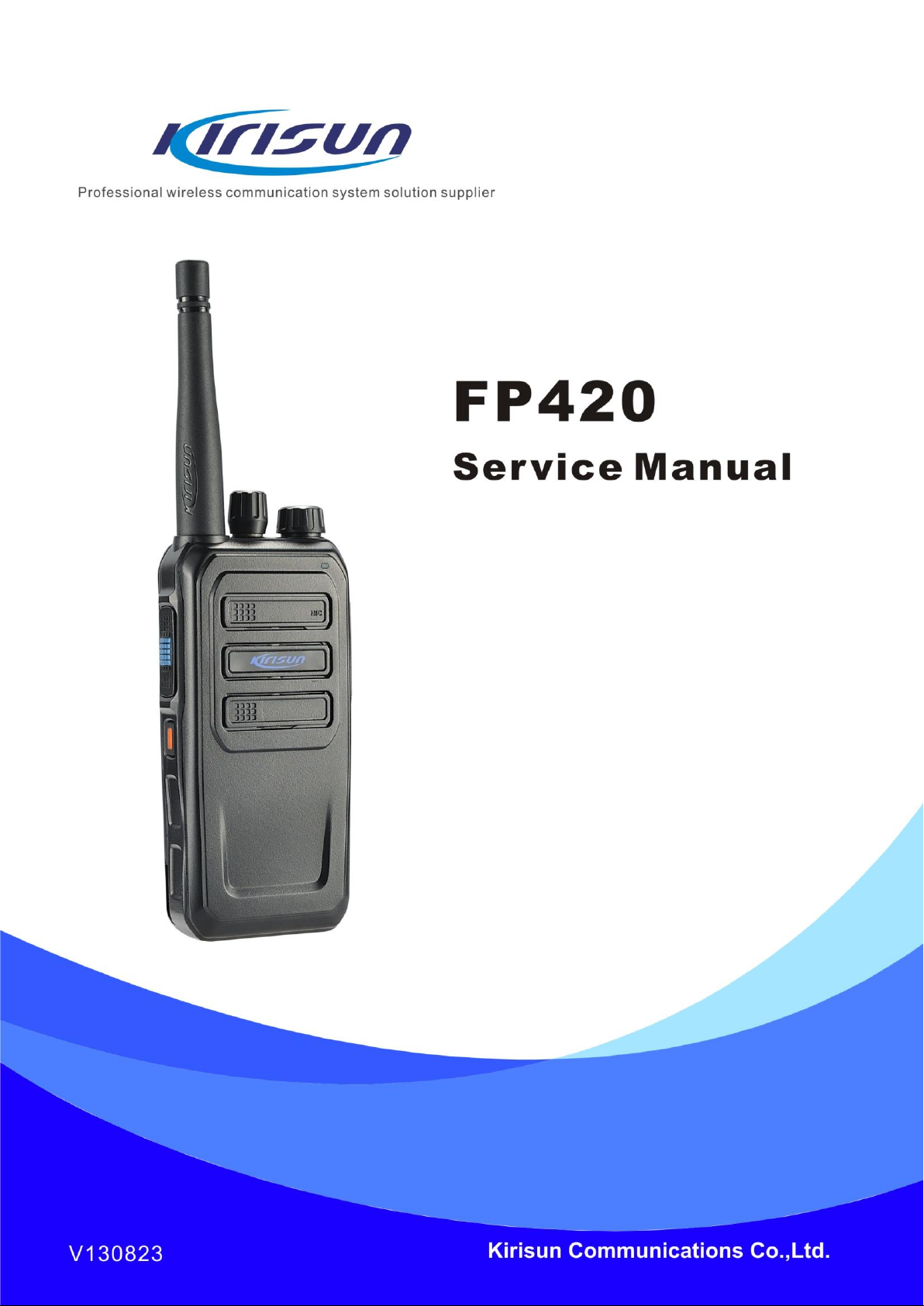
Chapter 2 External View and Functional Keys
2.1 External View and Functional Keys
Page 3 of 50
Page 5

FP420 Service Manual
Figure 2.1
1
○
Antenna
2
○
PTT
Press the key and talk to make a call; release the key to listen
3
○
PF Button
The button can be assigned different functions through PC software by your dealer.
Details refer to the following “Programmable Key” in this instruction.
4
○
Speaker
Output the voice
5
○
Channel Knob
Rotate to choose 1—16 channels.
6
○
On/Off Key and Volume Knob
Clockwise rotate the knob to turn on the radio, and counterwise rotate the knob until
there is a click sound to turn off the radio.
Rotate the knob to adjust the volume when the radio is on.
7
○
LED Indicator
When transmitting signal it indicates red, when receiving signal it indicates green. It
flashes when the power is not enough.
8
○
Microphone
Input the voice
9
○
External Connector
Open the cover to connect external speaker and microphone.
10
○
Belt Clip
11
○
Pushing Buckle
2.2 Functional Keys Operation Instruction
Programmable Keys
Below keys can be set through PC software by dealers:
Long press key and short press key can be set: PFkey
Long press key can be set:Menue Key/ Cancel Key
NOTE:
Short press:Press down and release instantly.
Long press:Press down and keep 2 seconds to release.
Available functions to be chosen:
None:No feature will be assigned.
Power level adjustment: Switch between high/low power
Page 4 of 50
Page 6

FP420 Service Manual
Moniter: If the current analog channel is with CTCSS/CDCSS, press the key to squelch
mode to cancel the CTCSS/CDCSS function. Press the key again to return to the original
status.
Emergency alarm open: Start the Emergency Alarm function to seek help.
Emergency alarm close: Finish the Emergency Alarm function.
Squelch open/close: Open/close the squelch function to receive weak signal on analog
channels.
Scan: Check activity of other channels. Press the key to open/close this function.
Whisper: When the whisper function is on, others can hear clearly even speakomg in a
low voice.
Aler tone on/off: Open/close the alert tone.
2.3LED Indicator
Red LED lights on: the radio is transmitting.
Green LED lights on: the radio is receiving.
Red LED flashes: low battery, the battery needs to be charged.
2.4 Basic Operation
Turn On/Off the radio
Clockwise rotate the knob to turn on the radio, and counterwise rotate the knob until
there is a click sound to turn off the radio.
Selecting a channel
Each channel in your radio can be programmed to analog channel or digital channel.
Under the Home Screen, turn the Channel Knob to select a channel.
Adust the volume
Rotate the knob to adjust the volume when the radio is on.
Make a call
On a digital channel, choose one of the following procedures to make a call:
a. Enter Contacts menu, select one contact and then press and hold the PTT Button,
speak to the MIC.
b. Enter Call Log menu, and then enter Call Out or Call In item, select one contact,
press the PTT Button and speak to the MIC.
c. Under the Home Screen, press the PTT Button and speak to the MIC. The call out
number is the default contact number of this channel, which can be programmed by the
dealer, or set through menu.
d. Under the Home Screen, input the number manually, then press the PTT Button and
Page 5 of 50
Page 7
FP420 Service Manual
LPF
RDA1846
ANT
LT1801A
AF AMP
MIC
12.8MHZ
Q501 Q503
LNA
32.768KHz
FLASH
18.432MHz
APC
speak to the MIC.
On an analog channel, press the PTT Button and speak to the MIC.
Receiving a call
When receiving the signal, the signal strength will be indicated on LCD. While on
digital channels, when receiving private call/group call/all call, the radio will output the
voice. While on the analog channels, when receiving analog signal and the
CTCSS/CDCSS matches, the radio will output the voice.
Anserwing a call
While using digital channels, press PTT within call holding time after receiving the call
to answer the call. If you didn’t answer back during call holding time, you should start a
new call to call back. The call holding time can be set through PC software by dealers.
While using analog channels, press PTT to answer the call directly.
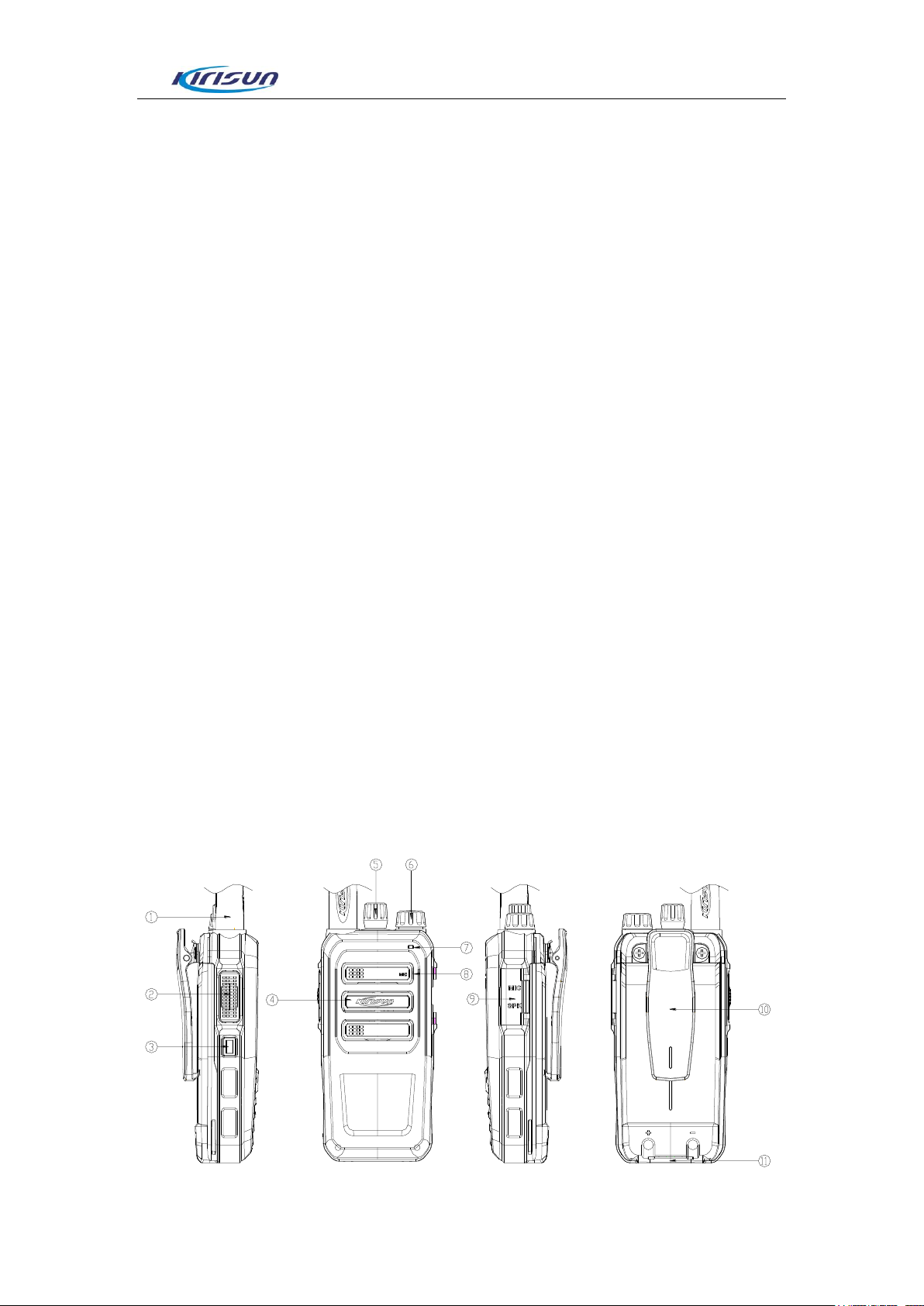
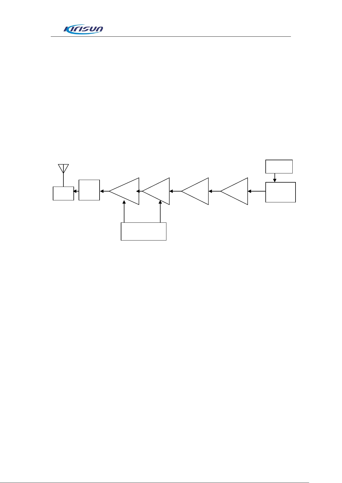
Chapter3 Circuit Description
3.1 Preface
This radio is FM portable radio equipment.
3.2 Frequency Configuration
The reference frequency of RD1846S is generated by 12.8MHz crystal oscillator X500
TCXO.
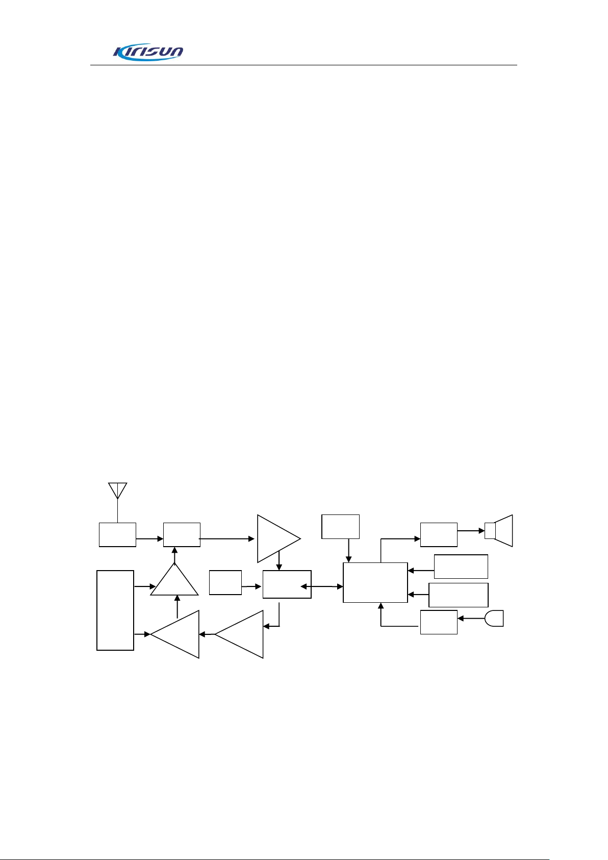
3.3 Principle of Receiver (RX)
Page 6 of 50
Page 8
FP420 Service Manual
LPF
ANT
SW
RDA1846
LT1801A
POWER
SW
AFAMP
LNA
Figure 3.3 Principle of Receiver
Receiver is mainly used in receiving, selecting, amplifying, transforming, demodulating
etc. and other processing like audio signal amplifying, filtering. Audio part mainly is used
to post emphasis, amplify and filter audio signal.
Receiver Front End
Low noise amplifier is located in the receiver front-end, mainly used in amplifying small
radio frequency signal, in order to provide certain intensity and SNR of RF signal for
subsequent signal processing.
Signals from the antenna transmission (RX/TX) switch (D502 D501, D503, D504), are
sent to Q507 3SK318 and peripheral components consisting of low noise amplifier (LNA)
for enlarging. The enlarged signal will be sent into IC4 (RDA1846S) to demodulate into
output audio signal. 3sk318 noise coefficient is 1.4 db, G about 18 db.
There is input and output match for LNA. Input match adopts best noise figure while
output use maximum power to match, i.e., the amplifier output impedance adjusted to the
load impedance (typically 50 ohm); Input and output impedance of the low noise pipe is
usually high impedance, so the matching circuit using inverted L
Receiver audio signal processing
Audio signal from IC4 (RDA1846S) processed through LT1801, then through the
volume potentiometer, to the audio power amplifier U600 (TDA2822).
Page 7 of 50
Page 9
FP420 Service Manual
LPF
RDA1846S
ANT
SW
12.8MHZ
Q501
Q500
Q503
Q502
APC
Audio power amplifier
U600 and peripheral components makes up the audio power amplifier circuit
Q601 base is the control end. High level: U2 begins to make audio; Low level: closed.
Receive audio signals, voice signals, alarm sound signals are summarized and sent to
speaker through audio power amplifier. Among them, the alarm sound will not be limited
by volume control. The speaker impedance: 16 ohms.
3.4 Principle of Transmitter (TX)
Power amplifier and antenna switch principle diagram
Modulated signal from IC4 (RDA1846S), enlarged via Q502, Q503, Q501, are sent to
Q500 power amplifier, and then transmitted through receiving toggle sending into the low
pass filter. LPF will improve as much as possible to harmonic stray signal attenuation in
certain condition of fluctuations in performance. Q500 output power: 4W
Q502 2sc5108 pre-amplifier, mainly to preliminary enlarge output RF signal of
RDA1846S, to provide a certain intensity of the amplifier after excitation signal.
Q503 2sc3356 pre-push RF amplifier is mainly used to provide a certain level of
intensity of excitation signal for subsequent amplifier, so as to guarantee the driving
amplifier can output enough power, to push the last stage power amplifier.
Q501 RD01 promote RF amplifier, is mainly used to promote the last stage power
amplifier, to ensure the output power of the last stage power amplifier to achieve the rated
output power of the transmitter. The output is about 0.5 W, G about 14 db.
Q500 RD07, end RF power amplifier, is part of the important and critical level. The
output power and efficiency level at the end power amplifier are almost equal to
transmitter output power and efficiency. The stability of the last stage amplifier basically
Page 8 of 50
Page 10

FP420 Service Manual
IC100
5T
5R
IC102
3.3V IC102
1.8V
1.8V:MCU;BASEBAND;LCD
3.3V:MCU;BASEBAND;LCD
5T:AF; BASEBAND, RF
5R:RF
represents the stability of the transmitter also. Output is 0.8W, G about 12db.
Q500 Q501 grid bias is controlled by APC circuit. Change the gate bias voltage, can
easily control the size of the transmitter output power.
APC (automatic power control) circuit
This circuit changes the gate bias voltage by testing the change of the input to the
power amplifier drain current and changes the output power by changing the gain.
R520 R521, R522 are power amplifier current detection, U502A is the current sampling
amplifier power amplifier. U502B is the comparison power amplifier.
If the transmitter output power is too large, the power amplifier current increase,
U502A output rise, U502B output voltage drops, applied to Q500, Q501 bias voltage to
drop, lower the transmitter output power, vice versa. In this way, the transmitter output
power is stable under different working conditions.
MCU achieves the goal of setting power by changing the input to the voltage on the
U502B.
Transmitter speech signal processing
MIC signal is sent through the inside and outside MIC switch circuit into No. 11 feet of
IC4 (RDA1846S) to modulate the carrier.
3.5 Principle of power
The machine uses 7.4 V batteries. Transmitter power amplifier circuit (Q500, Q501)
and receiver audio processing (U600) directly uses the battery. All the other circuits are
powered by constant 5 V power supply.
IC100: 5T switch, controlled by MCU.
Page 9 of 50
Page 11

FP420 Service Manual
5T: supply power for front-end transmitter
5 R: supply power for receiver RF amplifier, audio signal processing unit
etc.
IC102:3C switch controlled by MCU, Provide 3.3 V
3C: receive 3V electricity controlled by power save, supply power for
RDA1846S.
IC102: Provide VCC1.8V
3.6 IC characteristics
RDA1846S features:
3.6.1. Fully integrated CMOS RF front-end
3.6.2, High linearity and low noise amplifier and mixer
3.6.3. Low intermediate frequency receiving channel
Automatic DC offset calibration circuit
High performance analog/digital converter and digital/analog converter
Fully integrated receive filters
The digital AGC
The frequency modulation demodulation technology based on digital signal processing
technology
3.6.4 Direct frequency synthesis pathway
Direct frequency synthesis frequency modulation
Emission filter based on digital signal processing technology
FM digital gain adjustable
Digital voice activation emission control
3.6.5. High-performance decimal PLL frequency synthesizers
Complete piece RF VCO
The complete piece inside the loop filter
Low phase noise
Extremely fast phase lock time
High frequency resolution, frequency is adjustable
The built-in crystal frequency error calibration circuit
Page 10 of 50
Page 12
FP420 Service Manual
Pin
NO
I/O
Port
Name
function
E11
IO
SIRIN
SECRET_IO(Reserved for Encryption
chip)
D11
IO
SIROUT
POW_C(Soft switch on power control)
M4
IO
RXD1
RXD(Download program)
J4
IO
TXD1
TXD(Download program)
L4
IO
RXD2
EFUNC1(function key)
K4
IO
TXD2
EFUNC2(function key, monitor key)
A16
IO
SCLK0
GPS Enable Pin
A15
IO
SSN0
TX_LED(Transmitter indication)
B11
IO
SRX0
RX_LED(Receiver indication)
A11
IO
STX0
LAMP(keypad light)
N4
IO
SIMCK
PTT KEY(PTT)
R4
IO
SIMIO
EXT_PTT(PTT for earpiece)
P4
IO
SIMRST
Soft boot detection ( use this if you have
any other functions. Otherwise, please use
POW_ON
A8
IO
RFSO
RFIF Three line SPI serial data output
module
E9
IO
RFSN0
RFIF Modules chosen line of three SPI
piece inside signal is 0
C12
IO
AON
HEADSET_DET(headset detect)
B15
IOU
KB0
KB The keyboard scan input/output
signals [0-7], includes alarm and two
function keys. It is highly recommended to
refer to the design the of hardware
keyboard circuit to make it easier for
compatibility
B14
IOU
KB1
B13
IOU
KB2
B12
IOU
KB3
C16
IOU
KB4
C15
IOU
KB5
C14
IOU
KB6
C13
IOU
KB7
3.6.6. Ultra low power sleep mode
3.6.7. Three line serial digital interface control
3.7 semiconductor devices
MCU instructions
Table 3.7 the microprocessor (LT1801A) port
Page 11 of 50
Page 13

FP420 Service Manual
T3
IO
LCDCRD
LCD_RD
R3
IO
LCDCRS
LCD_RS
P3
IO
LCDCWR
LCD_WR
M3
IO
LCDCS0
LCD_CS
N3
IO
LCDCS1
LCD_RST
K1
IO
LCDC0
LCD_D0
L1
IO
LCDC1
LCD_D1
M1
IO
LCDC2
LCD_D2
A14
IO
SCLK1
SPEAKER_POP/AGC_PD(AGC enable
chip)
B16
IO
SSN1
APC
A13
IO
SRX1
A12
IO
STX1
RX_SW
A9
IO
PWM0
MOTO_EN 或 LAMP(Keypad light)
E10
IO
PWM1
LCD_BACK
E7
-
GPO0
P_UL(Indicate frequency lock state)
D7
GPO1
5T(TX power control)
C7
GPO2
5R(RX power control)
B7
GPO3
5C(Radio frequency (RF) public power
control)
CPU please don't use these 4 pins
D9
IO
RFSN1
P_PS(PLL lock indicator)
C9
IO
RFSN2
TX-SW
B5
IO
OSCEN
SPEAKER_EN
B8
IO
RFSCLK
RFIF (Three line SPI clock module )
P6
IO
NC
N1
IO
LCDC3
LCD_D3
P1
IO
LCDC4
LCD_D4
R1
IO
LCDC5
LCD_D5
T1
IO
LCDC6
LCD_D6
K2
IO
LCDC7
LCD_D7
L2
IO
LCDC8
LCD_D8
M2
IO
LCDC9
LCD_D9
N2
IO
LCDC10
LCD_D10
P2
IO
LCDC11
LCD_D11
R2
IO
LCDC12
LCD_D12
T2
IO
LCDC13
LCD_D13
K3
IO
LCDC14
LCD_D14
L3
IO
LCDC15
LCD_D15
G3
AI
Simulation of the
ADC module voltage
input range is 0 to 3 v
VO or VOX
F3
AI
battery voltage detection
E3
AI
RSSI
Page 12 of 50
Page 14
FP420 Service Manual
D3
AI
BUSY
F5
AO
RFIF
( AUXDA
)
Simulation of DAC
module input voltage
range of 1.15-2.15 V
VCCN(TCXO reference voltage)
E5
AO
RFIF
( AUXDA
)
Simulation of DAC
module voltage input
range is 0 to 3 v
TV/PC
D1
AI
RX_I+
Simulation of the
ADC module for
single-ended input
voltage range 1 VPP,
difference of 2, pp
AFDET
C1
AI
RX_I-
B1
AI
RX_Q+
Simulation of the
ADC module for
single-ended input
voltage range 1 VPP,
difference of 2, pp
A1
AI
RX_Q-
A2
IO
TX_I+
Simulation of DAC
module voltage
output range of
single-ended 1 VPP,
difference 2 VPP
MOD1
B2
IO
TX_I-
A4
IO
TX_Q+
Simulation of DAC
module voltage
output range of
single-ended 1 VPP,
difference 2 VPP
MOD2
B4
IO
TX_Q-
G2
IO
CODEC 16 Ohm 耳
机 headphones
negative output
CODEC 16 Ohm Headphones differential
negative output
H2
IO
CODEC 16 Ohm
headphones positive
output
CODEC 16 Ohm Headphones difference
negative output
H5
IO
CODEC The
microphone bias
voltage
MIXBIAS
J2
IO
SPEAKER Linear
output
SPEAKER Linear output
E2
AI
MIC input
input
amplitude=96mv
when 24dB open;
input
MIC2(headphone MIC input)
Page 13 of 50
Page 15
FP420 Service Manual
amplitude=1.53V
after closed
F2
AI
MIC input
input
amplitude=96mv
when 24dB open;
input
amplitude=1.53V
after closed
MIC1(headphone MIC input)
L5
D10
RXD0 (for GPS)
C10
TXD0 (for GPS)
B10
RTS0 (for GPS)
A10
CTSO (for GPS)
R5
K5
GPIO0_12 Hard boot detection
L7
L8
L9
L10 -
AVDD
1
Power supply
SCLK
2
Clock input for serial control bus
SDIO
3
Data input/output for serial control bus
AVDD
4
Power supply
XTAL1
5
Oscillator pin 1
XTAL2
6
Oscillator pin 2,control interface select
MODE
7
When MODE = VL, I2C Interface is select; When MODE =
VH, SPI Interface is select
SENB
8
Latch enable (active low) input for serial control bus
AFOUT
9
Audio signal output to speaker
NC*
10
No connection
MIC_IN
11
MIC input
Cc
12
Compensation capacitor connection
AVDD
13
Power supply
NC*
14
No connection
RFIN
15
RF signal input
AVDD
16
Power supply
NC*
17
No connection
RFOUT
18
RF signal output
RDA1846S port
Page 14 of 50
Page 16

FP420 Service Manual
NC*
19
No connection
NC*
20
No connection
AVDD
21
Power supply
PABIAS
22
PA bias supply for PA
AVDD
23
Power supply
PDN
24
Chip enable, high active; Chip sleep, low active
GPIO7
25
Gpio7/vox(When Gpio7=VH, vox is active; else VL)
GPIO6
26
Gpio6 / sq
(When Gpio6=VH, sq is active; else VL)
GPIO5
27
Gpio5 / txon
(When Gpio5=VH, txon is active; else VL)
GPIO4
28
Gpio4 / rxon
(When Gpio4=VH, rxon is active; else VL)
GPIO3
29
Gpio3 / sdo
(Gpio3=VH or VL, it is the output register data in 4 wire
control
Interface mode)
GPIO2
30
Gpio2 / int
(When Gpio2=VH, int is active; else VL)
GPIO1
31
Gpio1 / code_in / code_out
(Gpio1=VH or VL, it is the input/output code data)
GPIO0
32
Gpio0 / css_in / css_out
(Gpio0=VH or VL, it is the input/output CTCSS/CDCSS
signal)
Item
Model No.
Functions
U500
NJM2904
APC,
U400
LT1801A
MCU
IC200
24LC512
E2PROM , Storage channel frequency data, set
parameters, debugging status parameters
U201
TDA2822
Receiver audio power amplifier
Q500
RD07S2B
end of TX power amplifier
Q504
DTA144EE
APC output switch
Q507
3SK318
Receiver high power
Q200
DTC144EE
Red LED drive
Q201
DTC144EE
Green LED drive
Q501
RD01MUS1
Transmitter power amplifier
Q202
DTC144EE
Audio power amplifier control switch
U404
XC6204B502MR
The adjustable 5 R, 5 T voltage output
IC102
LN2407
1.8V output voltage adjustment
IC103
LN2407
3.3V output voltage adjustment
Q600
FMMT717
Audio output control switch
3.8 semiconductor devices functional description
Page 15 of 50
Page 17

FP420 Service Manual
Q205
DTC144EE
MIC Switch
Q501
2SC5108
TX 1st amplifier
Q503
2SC3356
TX 2st amplifier
Chapter 4 Function Description and Parameter
Settings
4.1TOT
This function forbids you from occupying the channel for a long time. If the continuous
transmitting time exceeds the setting time by dealer, the radio sends out a warning tone
and stops transmitting. Release the PTT key to stop the warning tone. After a period of
time, which is set by dealer, you can transmit again. And if the radio is programmed with
pre-alert function by the dealer, the radio will send out an alert before the time out timer
expires
4.2 Scan
During scan, the radio checks and stops on a busy channel. Then the radio continues
scanning until the channel is not busy for a while (this time is set by dealer, which is
named as Scan Hold Time).
Steps to start scanning: press the Scan shortcut key select “Start” item. The radio
scans the channels in the current scanning list one by one. During scan, press the Cancel
key or scan shortcut key to stop.
◆Scan revert channel
During scan, press the PTT key to make the radio transmit on a default channel. The
channel can be programmed by your dealer.
4.3Kill、Revive
This function allows one radio to receive the kill and revive signaling from another radio.
The radio to be killed cannot make or receive calls. The radio can only revive through CPS
sends a revive order. After revived, the radio can work normally again. This function is
used to manage the unauthorized usage of the radio, prevent misappropriating the radio
which is lost
4.4Emergency
If you are in danger and this function is enabled, you can press Emergency Alarm On
shortcut key to send an emergency alarm.
Page 16 of 50
Page 18

FP420 Service Manual
The means of sending emergency alarm are decided by the following parameters:
Alarm Type, which defines the audio and visual reaction when the radio sends an alarm;
Alarm Mode, which defines the content sent to the other members when the radio sends
an alarm. The above parameters can be programmed by dealer.
To turn off the Emergency Alarm, press the programmed Emergency Alarm Off
shortcut key.
Alarm Type:
◆None: No alarm function (Default setting); you cannot send an emergency alarm.
◆Siren Only: The radio only emits siren locally.
◆Regular: The radio provides audio and visual indication that it is in Emergency
mode and can receive the signal from others;
◆Secret: No audio and visual indication. And the radio cannot receive the signal from
others;
◆Secret with voice to follow: No audio and visual indication. But the radio can receive
the signal from others.
Alarm Mode:
◆Emergency Alarm: The radio sends out an emergency alarm, and then exits the
emergency alarm status automatically.
◆Emergency Alarm w/ Call: An emergency alarm is sent, after which an emergency
call can be transmitted by pressing the PTT Button.
◆Emergency Alarm w/ Voice to Follow: The radio sends out an emergency alarm, and
then sends out background tone periodically and automatically through emergency call.
Note:
Emergency Alarm: The radio sends out a signal to alert other member.
Emergency Call: A priority call on channel, so as to make sure the successful
communication under emergency condition.
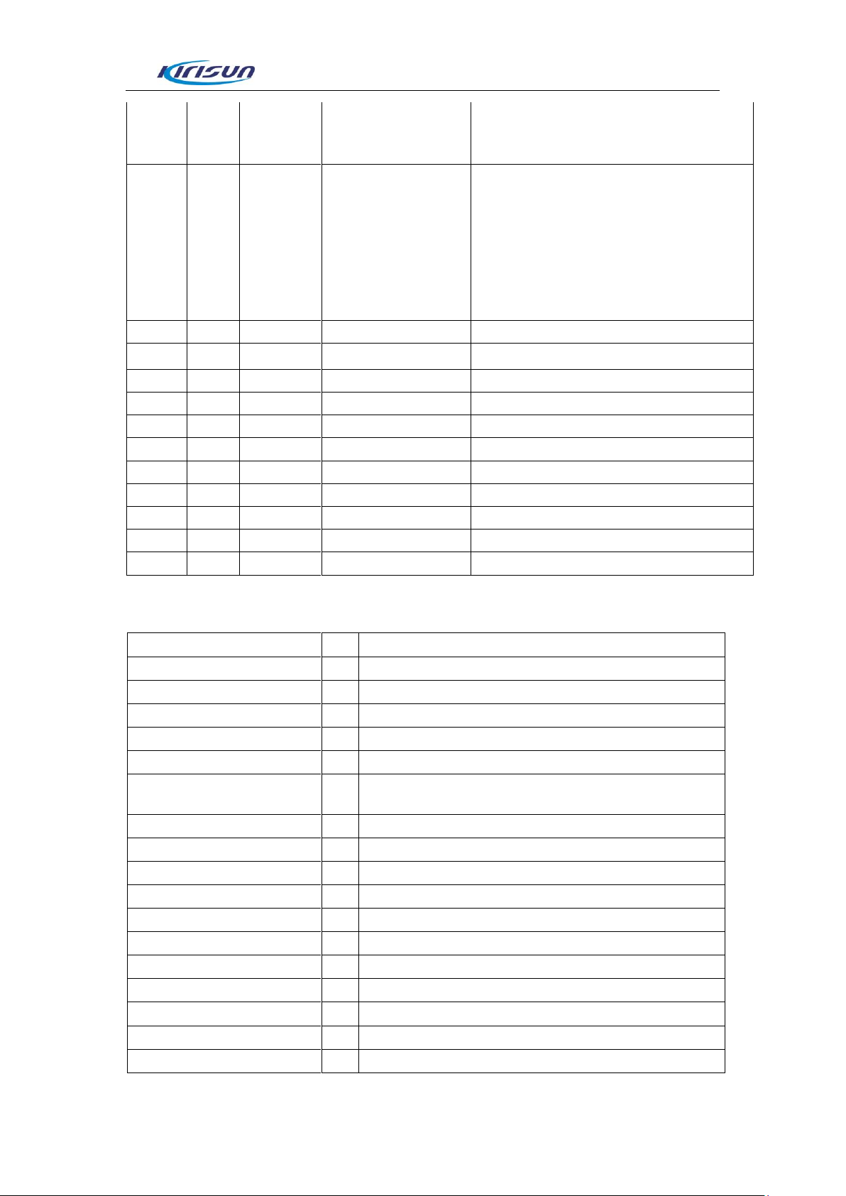
4.5 Parameter Setting(PC Mode)
The radio parameter have been programmed in the factory.The user can reset the
radio parameters such as working frequency, channels, digital functions, QT/DQT, and
auto scaning.We designed a user-friendly and convenient programming software CPSc to
set parameters on the radio. The programming steps are as following:
Install the programming software of FP420
B. Connect the radio to the computer serial port with the specified programming
cable,see figure4.5
Page 17 of 50
Page 19

FP420 Service Manual
Computer(RS232 or USB)
Specifiled programming
cable
Radio(Speaker/MIC
socket)
Figure4.5
C.Turn on the radio power
D.Click the CPSc to run the programming software.
E.Click read to read the data from radio.
G.About more details, please refer to help file or programming instrunction manual.
Chapter5 Disassembly for Repair
The radio is a piece of precision communication equipment. Please be careful when
disassembling the radio during service. The instructions for the disassembly are as
follows.
5.1 Disassemble the Battery
Removing the Battery
Make sure the radio has been turned off,
When you remove the battery, ①push the battery latch upwards ②battery will
upspring③remove it away from the radio. ④If the radio with belt, pls pull up the battery.
Installing the Battery
If the radio with belt, ①pls upspring the belt. ②Install the two bulges at the bottom of
the battery pack with the corresponding slots at the rear bottom of the radio. ③Push the
top part of the battery towards the radio to lock it until a click is heard.
Page 18 of 50
Page 20

FP420 Service Manual
Notice:
Do not short-circuit the battery terminals or dispose of batteries in fire.
Do not attempt to disassemble the case of the battery.
5.2 Installing/Removing the Antenna
Installing: Hold the base of the antenna and turn the antenna clockwise into the
connector on the top of the radio until it’s tightened.
Removing: Hold the base of the antenna and turn the antenna anti-clockwise and
remove it.
5.3 Installing/Removing the Belt Clip
Match the grooves of the belt clip to the rear top of the battery, fixed it with two 2.5x6.5
screws. Loosen the two screws fixing clip, you can remove the clip.
Page 19 of 50
Page 21

FP420 Service Manual
Installing an optional headset
When you use an external headset, to open outward headphones cover in the upper
right of the radio, plug the external headphone cable into the headset port.
5.4 Removing the Back Cabinet from the Chassis
(1) Remove the antenna;
(2) Remove two screws on the knob and the screw on the antenna;
(3) Remove the two screws on the back cabinet;
(4) Remove those four screws on the Al alloy bracket;
(5) Insert the flat-bladed screwdriver into the slot of Al alloy bracket; lift it so as to
separate the Zinc alloy bracket from the chassis, and then push the Al alloy bracket away
from the chassis, and take the soft flat cable away from the socket. Using the soldering
iron to separate the speaker connecting cable.
Page 20 of 50
Page 22

FP420 Service Manual
5.5 Removing the PCB Board from the Chassis
(1) Screw off screws on the main board
(2) Take down the waterproof cushion in top and use the soldering iron to cut off the
antenna connecting point, and then separate the main board (include PTT PCB) from the
aluminium alloy chassis.
Page 21 of 50
Page 23

FP420 Service Manual
After the demolition of the above, you can make the appropriate repairs and debugging
against fault conditions.
5.6 Exploded view
Page 22 of 50
Page 24

FP420 Service Manual
No. Part Code
Part Name
Specifications
Unit
1
7MHP-4038-06A-W0
FP420
Headphone
cover
TPU; Black; texture
1
2
7MJS-4038-01A-W0
FP420 spindle
SUS304;nature color, BaYang,
Non-lead
1
3
7MHP-4038-01A-W0
FP420 Surface
shell
PC+ABS; Black; texture
1
4
7MHB-7069-01A-W0
PT7800
Microphones
waterproof pad
DY-E002A Breathable
film,φ6.6xφ4.4,
1
5
7GCB-S4002-01A
4700 Speaker
dust –proof
No anti-cloth; black; Xinlongda;
non-lead
1
Page 23 of 50
Page 25

FP420 Service Manual
cover
6
7PLJ-4038-E01A
S760
Trademark
stickers
Transparent PC
1
7
7MHR-4038-01A-W0
FP420 Side
silicone key
Silica gel; black; Laser carving;
PT Orange21C;
1
8
7NRC-060090035-W
1
FP420 Coding
nut
Brass, diameter M6mm, OD
φ9mm, thick 3.5mm, black nickel
plated
1
9
7NRC-090115025-G1
3208 nut
Brass, diameter M9mm, OD
φ11.5mm, 2.5mm thick
1
10
8ATX-400470-WU
FP420 Antenna
428649,Φ=40mm,H=4.5mm
1
11
7MHR-4038-03A-WC
FP420 Light
pipe
Silica gel; transparent; high light;
MingKun; Non-lead
1
12
7MHP-4038-05A-W0
FP420 PTT
Cover
Double Color
1
13
4SS7-3525-016-100B
7200 Speaker
Φ40mm,1W,Non-lead
1
14
7MHS-4038-02A-W
FP420PTT
keypad metal
dome
φ5mm,SUS301 Round metal
dome;
1
15
7MHJ-4038-03A-W
FP420
Double-sided
adhesive side
key board
3M9448
1
16
7MHR-1727-09A-W3
558 radio mic
sets
Silica, hardness 40, orange, no
surface treatment
1
17
7MDC-4057-02A-G
FP420 Battery
SLC
Material: Brass; nickel-plated
gold-covered
4
18
7MHR-4038-04A-W0
FP420 Top
waterproof pad
Silica gel; black; polishing
1
19
7MHP-4038-03A-W0
FP420 Volume
knob
ABS; Black; texture, white-oil
1
20
7MHS-1140-01A-W
3118/3208
Knob retainer
Spring steel
2
Page 24 of 50
Page 26

FP420 Service Manual
21
7MHP-4038-04A-W0
FP420 Coding
knob
ABS; Black; texture, white-oil
1
22
3CR7-SMA-50JF-4
RF coaxial
connectors
SMA-J, Flange mounting,used
for 7200
1
23
7MDZ-1737-04A-J5
KB-58L sticker
1
Dark green paper,8*35mm,thick
0.2mm, single Side with plastic
2
24
6BPM-784043-07415
0-A
Li-poly battery
pack (FP420)
Li-poly battery pack 78mm*
40mm*4.3mm×2,7.4V,1500mAh
1
25
7GCM-360075040-J
KB-36L Foam
pad
Black foam,36*7.5*4mm, single
Side with plastic
1
26
7MHP-4038-02A-W0
FP420 Top
Cover
PC+ABS; Black; texture,
1
27
7SMF-020080M-MHH
T-N1
M2*8
Plum-type
Thick Head
Machine Screw
Iron and hard, Φ2mm * 8mm
thick plum-type nickel-plated
machine
Metric Coarse, drop-resistant
treatment
1
28
6SS3-BJ4038-A
KBJ-17 Belt
1
29
7MDP-4057-01A-W0
KB-460 Battery
top shell
PC+ABS; Black; texture,
1
30
6PD7-4057-DPA
KB-460 Battery
charging board
PCB,29.4X11.3MM, Thickness:
0.6MM,2 layers
1
31
7MHP-4038-10A-W0
FP420 Power
on Right hook
POM; Black; high light
1
32
7MHC-4038-01A-Z
FP420 Power
on splinter
T=0.20 Spring steel; black zinc
plated; Xinchengda; Non-lead
1
33
7MHP-4038-09A-W0
FP420 Power
on left hook
POM; Black; high light
1
34
7MHP-4038-08A-W0
FP420 Power
on Push Button
PC+ABS; Black; texture,
1
35
7SMF-020080M-MHH
T-N1
M2*8
Plum-type
Thick Head
Machine Screw
Iron and hard, Φ2mm * 8mm
thick plum-type nickel-plated
machine
Metric Coarse, drop-resistant
1
Page 25 of 50
Page 27

FP420 Service Manual
treatment
36
7MDP-4057-02A-W0
KB-460 Battery
case back
PC+ABS; Black; texture,
1
37
7MHR-4038-02A-W0
FP420 main
Waterproof
gasket
Silica gel; black; high gloss
1
38
7MHR-4038-05A-W0
FP420
Bomb-pin
socket
Silica gel; black; polishing
1
39
7MHL-4038-01A-W
FP420
Aluminum
ADC12;
1
40
7MHP-4038-07A-W0
FP420
Headphone
jack waterproof
pad
TPU; Black; texture,
1
41
7SMF-020040M-SZY
B-N
M2*4 Cross
round flat head
Machine Screw
Iron and hard,Φ2mm*4mm
Cross round flat head
Nickel-plated machine, Metric
Coarse, plus drop-resistant
treatment
8
6.1 Method of Adjustment
During the servicing, it is necessary to test and adjust the radio’s technical parameters
after changing components.
6.1.1 Components needed for the adjustment
(1) Antenna connector converter
(2) Universal connector
6.1.2 Adjustment Method in PC Testing Mode
Tx Part
A.Tx Frequency
Chapter 6 Adjustment
Page 26 of 50
Page 28

FP420 Service Manual
Frequency
(136-174) MHz
(400-470)MHz
The Tx frequency is the standard frequency ± 100Hz.
B. Power
a. High Power is 3.5-5.0W.
b. Low Power is 0.5-1.5W.
C. Voltage
Voltage is 6.5V.
Rx Part
A. Max Volume
Set RF of the comprehensive tester to be the center frequency, the single strength
to be 1mV and the modulation deviation to be 3.0kHz/1.5kHz (wide/narrow band), and
then in PC mode, adjust the value of “Max. Volume” to make the audio power to be
1.0-1.2W.
B. Squelch
a. Set the RF signal of the comprehensive tester to be -121dBm, and the deviation
3.0kHz/1.5kHz(wide/narrow band).In PC mode, adjust the SQL of the 5 frequency points,
and save it when the data is stable.
b. Set the RF signal of the comprehensive tester to be -123dBm, and the deviation
3.0kHz/1.5kHz(wide/narrow band).In PC mode, adjust the SQL of the 5 frequency points,
and save it when the data is stable.
Chapter7 Major Specification
7.1 General Specification
Page 27 of 50
Page 29

Usable sensitivity (12dB SINAD)
-121dBm
Squelch On sensitivity
≤0.18uV
Adjacent Channel Selectivity
≥70dB/≥60dB
Intermodulation Rejection
≥65dB
Spurious response rejection
≥70dB
Audio output power
1W,Balance @ Distortion ≤5, 16Ω
Rx current consumption
≤400mA
Tx power
4.0W/1.0W @7.4V DC
Frequency stability
≤±2.5ppm
Max. modulation deviation
±3kHz/±1.5kHz
Modulation distortion
(300~3000Hz)
≤3%
Adjacent channel Tx power
≥60dB/≥55dB
Spurious Tx
≥70 dB
Tx current consumption
≤1.4A @ 7.4V DC
Model
FP420
Number of Control Channel
16 Zones x 16 Channels
Channel spacing
25kHz/12.5kHz
Operating voltage
7.4V, cathode grounded
Operating temperature
-25°C ~ +55°C
Antenna impedance
50 Ω
Microphone impedance
2.2 Ω
Battery (Standard)
Li-ion Battery: DC 7.4V, 1500mAh,
Operating time: 12.5h (5: 5: 90 cycle)
Size (H*W*D)
116 mm x54 mm x30 mm
Weight (g)
240 (with battery and antenna)
7.2 RX Part
FP420 Service Manual
7.3 TX Part
Chapter 8 Service and Test Equipment
Page 28 of 50
Page 30

FP420 Service Manual
No.
Equipments
Specifications
1
Standard signal
generator
Frequency range: 400-470MHz
Modulation: FM and external modulation
Output: -127dBm/0.1 uV to >-47dBm/1mV
2
Power meter
Output impedance: 50 Ω
Operative frequency: 400-470MHz
Measuring range: around 10W
3
Deviation meter
Frequency range: 400-470MHz
4
Digital voltmeter
Measuring range: DC 10mv – 10v
Input impedance: load high input impedance to Min. circuit
5
Oscilloscope
Current to 30MHz
6
High sensitivity
frequency counter
Measuring range: 50Hz – 10KHz
Frequency stability: 0.2 ppm or lower
7
Ammeter
5A
8
Audio frequency
voltmeter
Frequency range: 50Hz – 10KHz
Voltage range: 1mv – 10v
9
Audio frequency
generator
Frequency range: 50Hz – 5KHz or higher
Output: 0- 1v
10
Distortion tester
Capacity: 3% or lower @ 1KHz
Input power level: 50mV to 10vms
11
Spectrum analyzer
Measuring range: DC – 1GHz or higher
12
Path generator
Center frequency: 50KHz – 600MHz
Output voltage: 100mv or higher
13
16 Ω dummy load
Around 16Ω, 3W
14
Adjustable power
supply
5v – 10v, around 5A
During the servicing and test process, the following equipments and apparatus will be
used:
Chapter 9 Troubleshooting
Page 29 of 50
Page 31

FP420 Service Manual
No.
Problems
Causes and solutions
1
Power ON failure
A. The battery pack may be out of power. Please
charge it or change a new one
B. Power switch in failure. Change a new one.
C.MCU in failure. Change the IC.
D. Zener diode Q45 is broken. Change a new IC.
2
PPL unlocked
(beeping)
A. The PLL crystal oscillator X500 is broken. Please
change it.
B. The RDA1846 is broken. Please change it.
3
Cannot talk to or hear
other
radios
A. The frequency of the radio’s current channel is not
the same with that of the other radio. Please reselect
a channel.
B. The CTCSS/DCS is not the same. Please reset it.
C. The radio is out of the effective communication
range.
4
No signal
A. The antenna is in poor contact. Please fasten it.
B. Low sensitivity, fine tuning “Regulating Mode”
C. The squelch level is too high, so the squelch
cannot be opened. Please adjust the squelch level.
5
The indicator lights
red while transmitting,
but no voice is heard
by the recipient.
A. The power amplifying tube is broken, so there is no
power output. Please change it.
B. The MIC is broken. Please change it.
C. The operational amplifier U600 is broken. Please
change it.
6
The indicator lights
green while receiving,
but no sound is heard.
A. The speaker is broken. Please change it.
B. The audio power amplifier U600 is broken. Please
change it.
C. The switch diode Q601 is broken. Please change
it.
7
The programming is
abnormal
A. The programming cable is not correctly connected
to PC. Please check the cable connection.
B. The Computer’s RS-232 serial port output is
Page 30 of 50
Page 32

FP420 Service Manual
abnormal. Please check the computer.
C. The earphone jack of the radio is in poor contact.
Please check the earphone jack. If it is abnormal,
please change it.
Part No.
Name
Specification
Q’ty
Pulg-in Position
6SS2-4038-HMB
S760 mainboard patches
parts
S760 mainboard patches parts,
no Pb
1
6SS1-4038-HMB
S760-02 mainboard
patches parts (Version
D)
400-470MHZ,S760-02 mainboard
patches parts, no Pb
1
0SS1-4038-HMD
S760 mainboard patches
parts
S760 mainboard patches
parts,1846S, no Pb
1
Appendix1 Abbreviation
AMP amplify, amplifier
ANT antenna
APC automatic power control
BPF band pass filter
CTCSS continuous tone control squelch system
DCS Digital code squelch
DEMOD demodulation
HPF high pass filter
IDC instantaneous deviation control
IF intermediate frequency
LED Light-Emitting Diode
LNA low noise amplifier
LPF low pass filter
MCU micro control unit
MIC microphone
MOD modulation
MONI monitor
PLL phase lock loop
PTT push-to-talk
SPK speaker
TCXO temperature control X’ oscillator
UL un-lock
VCO voltage control oscillator
Appendix 2 Electronic Parts List
Page 31 of 50
Page 33

FP420 Service Manual
3CF1-BL112-30RU
FFC/FPC connector
0.5mm spacing,30 Pin, horizontal
type
1
J201
1DP1-BV08C
R protected diode
BV08C
2
D600,D601
1DR1-NSR1020MW2T1
G
Surface mounting
schttky diode
NSR1020MW2T1G, No Pb
2
D101,D102
1DS1-DA2S10100L
R Surface mounting
switch diode
DA2S10100L
1
D505
1DS1-HSC277
R Surface mounting
switch diode (production
halts)
HSC277,1608
1
D502
1DS1-HVC131
R Surface mounting
switch diode (production
halts)
HVC131(P1),1608
2
D500,D501
1DZ1-HZU5ALL
R Surface mounting
constant voltage diode
(production halts)
HZU5ALL,2012,5V
1
D504
1IL1-NJM2904V
R Surface mounting
linearity IC
Double arithmetic amplification
NJM2904V,TSSOP-8
2
IC301,IC500
1IM1-AT24C512C
Surface mounting
memorizer IC
1IM1-AT24C512BN
(replaceable)
AT24C512C,
manufacture:ATMEL, no Pb
1
IC200
1IM1-DS28E10P
Surface mounting
memorizer IC
Encryption chip, DS28E10P+, no
Pb
1
U201
1IM1-M36LOT7050T3ZA
Q
Surface mounting
memorizer IC
M36LOT7050T3ZAQF, no Pb
1
U401
1IP1-LT1801A
Baseband process
module
1 U400
1IS1-MP2359
Surface mounting power
supply IC
MP2359,6PIN,1.2A
24V,1.4MHz,TSOT-23-6
2
IC102,IC103
1IS1-RDA1846S
Surface mounting
exclusively IC
RDA1846S,PLL module IC ,
5*5mm,32PIN,QFN32, no Pb
1
U500
1IS1-TDA2822
E R Surface mounting
exclusively IC
TDA2822
1
U600
1IS1-XC6204B502MR
R Surface mounting
constant voltage IC
Constant voltage integration
5V,SOT-23-5
1
IC100
1TF1-2SK1824
R FET
2SK1824(B1)
1
Q506
1TF1-3SK318
R dual-gate fet
3SK318(YB-)
1
Q507
1TF1-RD01MUS2
E R FET
1 Q501
1TF1-RD07MUS2B
E R FET
Mitsubishi, RD07MUS2B, no Pb
1
Q500
1TF1-ST2302
R FET
ST2302,SOT-23
2
Q602,Q603
1TT1-2SA1586
R Surface mounting
triode
2SA1586
1
Q605
Page 32 of 50
Page 34

FP420 Service Manual
1TT1-2SC3356-R24
R Surface mounting
triode
2SC3356-R24,SOT23,NPN
1
Q503
1TT1-2SC5108-Y
R Surface mounting
triode
2SC5108-Y(MC),NPN
1
Q502
1TT1-DTA144EE
R Surface mounting
triode
Digital triode, DTA144EE-SMD
1
Q504
1TT1-DTC144EE
R Surface mounting
triode
Digital triode,
DTC144EE(26),SOT323
9
Q1,Q101,Q103,Q200,Q201,
Q505,Q601,Q604,Q606
1TT1-FMMT717TA
R Surface mounting
triode
FMMT717A,PNP,SOT23
1
Q600
1TT1-KTA1298-Y
R Surface mounting
triode
KTA1298-Y,SOT23
2
Q100,Q102
2CC1-10-C0G500-101J
R flake multilayer
capacitor
1005,100P±5%,50V,C0G
19
C3,C4,C5,C7,C8,C9,C10,C1
1,C24,C225,C237,C238,C23
9,C240,C241,C242,C243,C5
21,C543
2CC1-10-C0G500-151J
R flake multilayer
capacitor
1005,150P±5%,50V,C0G
2
C301,C561
2CC1-10-C0G500-180J
R flake multilayer
capacitor
1005,18P±5%,50V,C0G
1
C520
2CC1-10-C0G500-220J
R flake multilayer
capacitor
1005,22P±5%,50V,C0G
3
C313,C314,C518
2CC1-10-C0G500-470J
R flake multilayer
capacitor
1005,47P±5%,50V,C0G
2
C558,C560
2CC1-10-C0G500-4R0C
R flake multilayer
capacitor
1005,4P±0.25P,50V,C0G
7
C315,C316,C317,C318,C319
,C320,C321
2CC1-10-C0G500-5R0C
R flake multilayer
capacitor
1005,5P±0.25P,50V,C0G
1
C310
2CC1-10-X7R100-105K
R flake multilayer
capacitor
1005,1μF±10%,10V,X7R
4
C219,C220,R606,R607
2CC1-10-X7R160-104K
R flake multilayer
capacitor
1005,100nF±10%,16V,X7R
29
C16,C100,C101,C111,C114,
C117,C127,C223,C224,C228
,C229,C300,C302,C303,C30
4,C305,C306,C307,C309,C3
11,C312,C322,C323,C324,C
325,C400,C601,C608,C616
2CC1-10-X7R160-333K
R flake multilayer
capacitor
1005,33nF±10%,16V,X7R
1
C583
2CC1-10-X7R250-223K
R flake multilayer
capacitor
1005,22nF±10%,25V,X7R
1
C584
2CC1-10-X7R500-102K
R flake multilayer
capacitor
1005,1000P±10%,50V,X7R
11
C120,C124,C226,C512,C536
,C545,C547,C562,C563,C57
3,C581
Page 33 of 50
Page 35

FP420 Service Manual
2CC1-10-X7R500-103K
R flake multilayer
capacitor
1005,10nF±10%,50V,X7R
11
C110,C112,C115,C126,C308
,C529,C539,C540,C548,C60
0,C612
2CC1-10-X7R500-471K
R flake multilayer
capacitor
1005,470P±10%,50V,X7R
76
C1,C29,C34,C40,C42,C44,C
46,C48,C50,C52,C102,C104,
C113,C118,C122,C128,C130
,C201,C202,C203,C204,C20
6,C207,C208,C209,C210,C2
11,C213,C214,C215,C217,C
218,C221,C222,C230,C231,
C232,C233,C234,C326,C332
,C519,C522,C523,C526,C52
7,C528,C530,C531,C532,C5
33,C535,C537,C
2CC1-16-C0G500-120J
R flake multilayer
capacitor
1608,12P±5%,50V,C0G
1
C507
2CC1-16-C0G500-1R0C
R flake multilayer
capacitor
1608,1P±0.25P,50V,C0G
1
C534
2CC1-16-C0G500-1R5C
R flake multilayer
capacitor
1608,1.5P±0.25P,50V,C0G
1
C504
2CC1-16-C0G500-220J
R flake multilayer
capacitor
1608,22P±5%,50V,C0G
1
C502
2CC1-16-C0G500-270J
R flake multilayer
capacitor
1608,27P±5%,50V,C0G
1
C510
2CC1-16-C0G500-2R0C
R flake multilayer
capacitor
1608,2P±0.25P,50V,C0G
1
C503
2CC1-16-C0G500-3R0C
R flake multilayer
capacitor
1608,3P±0.25P,50V,C0G
2
C514,C516
2CC1-16-C0G500-3R5C
R flake multilayer
capacitor
1608,3.5P/3.6±0.25P,50V,C0G
1
C505
2CC1-16-C0G500-4R0C
R flake multilayer
capacitor
1608,4P±0.25P,50V,C0G
1
C501
2CC1-16-C0G500-5R0C
R flake multilayer
capacitor
1608,5P±0.25P,50V,C0G
2
C513,C515
2CC1-16-C0G500-6R0D
R flake multilayer
capacitor
1608,6P±0.5P,50V,C0G
1
C509
2CC1-16-C0G500-8R0C
R flake multilayer
capacitor
1608,8P±0.25P,50V,C0G
1
C508
2CC1-16-X7R500-471K
R flake multilayer
capacitor
1608,470P±10%,50V,X7R
1
C511
2CC1-20-X7R6R3-475K
R flake multilayer
capacitor
2012,4.7uF±10%,6.3V,X7R(GRM
219R6J475KE19D)
2
C27,C542
2CC1-20-Y5V160-106Z
flake multilayer capacitor
2012,10uF+80%/-20%,16V,Y5V
18
C2,C103,C108,C116,C121,C
123,C131,C200,C205,C212,
Page 34 of 50
Page 36

FP420 Service Manual
C216,C227,C582,C602,C606
,C615,C119,C129
2CT1-TS35-100-470M
R Surface mounting
Tantalum capacitor
3528,47μF±20%,10V,TS
Series(Grade B)
1
C605
2LH1-R401R5-R03-05
R Surface mounting Air
Coil
Wire diameter: φ0.40, Inner
diameter: φ1.5, 3 circles, Pin
hight: 0.5mm, clockwise circling
4
L500,L501,L503,L505
2LH1-R401R5-R04-05
R Surface mounting Air
Coil
Wire diameter: φ0.40, Inner
diameter: φ1.5, 4 circles, Pin
hight:: 0.5mm, clockwise circling
1
L502
2LH1-R401R5-R08-05
R Surface mounting Air
Coil
Wire diameter: φ0.40, Inner
diameter: φ1.5, 8 circles,
clockwise circling, high Pin
1
L507
2LH1-R501R5-L05-05
R Surface mounting Air
Coil
Wire diameter: φ0.50, Inner
diameter: φ1.5, 5 circles,
anticlockwise, high Pin
1
L506
2LL1-16-12NJ
R multi-layer inductance
1608,12nH±5%(MLG1608B12NJ/
LL1608-FH12N)
1
L511
2LL1-16-18NJ
R multi-layer inductance
1608,18nH±5%(MLG1608B18NJ)
1
L509
2LL1-16-3N3S
multi-layer inductance
1608,3.3nH±0.3nH(MLG1608B3
N3S)
1
L504
2LW1-16UC-270J
R Surface mounting wire
wound inductance
1608, 27nH±5%, Ceramic core
(C1608CB-27NJ)
2
L3,L6
2LW1-16UC-680J
R Surface mounting wire
wound inductance
1608,68nH±5%, Ceramic core
(C1608CB-68NJ)
1
L516
2LW1-20UC-221J
R Surface mounting wire
wound inductance
2012,220nH±5%, Ceramic core
(LQN21AR22J/LQW2BHNR22J0
3L)
1
L508
2LW1-25UC-103J
R Surface mounting wire
wound inductance
2520,10μH±5%, Ceramic core
(FLM2520-100J)
1
L520
2LW1-35UF-473K
Surface mounting wire
wound inductance
3.5*3.0*2.1,47UH±10% ,CD32-47
0K,no Pb
2
L107,L110
2RE1-10-1502
Surface mounting exact
Resistor
1005,15KΩ±1%
1
R23
2RE1-10-1602
Surface mounting exact
Resistor
1005,16.2K±1%
1
R106
2RE1-10-4909
Surface mounting exact
Resistor
1005,49.9K±1%
1
R104
2RE1-10-6409
Surface mounting exact
Resistor
1005,64.9K±1%
1
R113
2RE1-10-8006
Surface mounting exact
Resistor
1005,80.6K±1%
1
R112
Page 35 of 50
Page 37

FP420 Service Manual
2RE1-16-1503
R Surface mounting
exact Resistor
1608,150K±1%
7
R517,R518,R519,R524,R525
,R527,R528
2RS1-10-000O
R Chip Resistor
1005,0Ω
26
R3,R4,R5,R6,R17,R19,R26,
R31,R32,C577,R251,R252,R
109,R306,R312,R339,R404,
R504,R516,R555,R624,C19,
C25,C569,C570,C607
2RS1-10-100J
R Chip Resistor
1005,10Ω±5%
4
R2,R244,R300,R559
2RS1-10-101J
R Chip Resistor
1005,100Ω±5%
6
R317,R318,R319,R320,R321
,R322
2RS1-10-102J
R Chip Resistor
1005,1K±5%
35
R8,R9,R108,R209,R210,R21
1,R212,R213,R214,R215,R2
16,R217,R219,R228,R236,R
237,R238,R239,R310,R502,
R506,R533,R534,R535,R536
,R537,R538,R539,R544,R54
5,R547,R551,R560,R622,R6
23
2RS1-10-103J
R Chip Resistor
1005,10K±5%
14
R100,R103,R110,R114,R226
,R235,R245,R307,R314,R40
0,R601,R613,R616,R617
2RS1-10-104J
R Chip Resistor
1005,100K±5%
18
R107,R220,R221,R224,R225
,R229,R231,R232,R233,R23
4,R309,R311,R324,R325,R3
26,R402,R403,R549
2RS1-10-105J
R Chip Resistor
1005,1M±5%
1
R526
2RS1-10-152J
R Chip Resistor
1005,1.5K±5%
1
R507
2RS1-10-153J
R Chip Resistor
1005,15K±5%
3
R302,R304,R542
2RS1-10-154J
R Chip Resistor
1005,150K±5%
1
R550
2RS1-10-182J
R Chip Resistor
1005,1.8K±5%
1
R20
2RS1-10-183J
R Chip Resistor
1005,18K±5%
2
R301,R303
2RS1-10-184J
R Chip Resistor
1005,180K±5%
1
R553
2RS1-10-220J
R Chip Resistor
1005,22Ω±5%
6
R1,R7,R33,R511,R543,R604
2RS1-10-221J
R Chip Resistor
1005,220Ω±5%
3
R249,R250,R548
2RS1-10-222J
R Chip Resistor
1005,2.2K±5%
7
R101,R102,R248,R305,R600
2RS1-10-223J
R Chip Resistor
1005,22K±5%
2
R27,R614
2RS1-10-271J
R Chip Resistor
1005,270Ω±5%
1
R505
2RS1-10-273J
R Chip Resistor
1005,27K±5%
1
R531
2RS1-10-274J
R Chip Resistor
1005,270K±5%
1
R105
2RS1-10-204J
R Chip Resistor
1005,200K±5%
1
R340
2RS1-10-330J
R Chip Resistor
1005,33Ω±5%
1
R510
2RS1-10-333J
R Chip Resistor
1005,33K±5%
2
R609,C611
2RS1-10-334J
R Chip Resistor
1005,330K±5%
1
R315
Page 36 of 50
Page 38

FP420 Service Manual
2RS1-10-392J
R Chip Resistor
1005,3.9K±5%
1
R514
2RS1-10-393J
R Chip Resistor
1005,39K±5%
1
R512
2RS1-10-470J
R Chip Resistor
1005,47Ω±5%
1
R500
2RS1-10-471J
R Chip Resistor
1005,470Ω±5%
2
R15,R612
2RS1-10-472J
R Chip Resistor
1005,4.7K±5%
2
R561,R562
2RS1-10-473J
R Chip Resistor
1005,47K±5%
19
R202,R203,R204,R205,R206
,R207,R208,R227,R240,R24
1,R242,R243,R501,R508,R5
13,R540,R541,R557,R558
2RS1-10-474J
R Chip Resistor
1005,470K±5%
1
R605
2RS1-10-561J
R Chip Resistor
1005,560Ω±5%
1
C578
2RS1-10-562J
R Chip Resistor
1005,5.6K±5%
1
R503
2RS1-10-563J
R Chip Resistor
1005,56K±5%
1
R529
2RS1-10-820J
R Chip Resistor
1005,82Ω±5%
1
R316
2RS1-10-822J
R Chip Resistor
1005,8.2K±5%
2
R308,R22
2RS1-10-823J
R Chip Resistor
1005,82K±5%
1
R509
2RS1-16-000O
R Chip Resistor
1608,0Ω
8
L7,L100,L103,L105,L108,L10
9,L111,L510
2RS1-16-153J
R Chip Resistor
1608,15K±5%
1
R515
2RS1-20-000O
R Chip Resistor
2012,0Ω
2
C337,L104
2RS1-32-000O
R Chip Resistor
3216,0Ω±5%
1
F100
2RS1-32-R47J
R Chip Resistor
3216,0.47Ω±5%
3
R520,R521,R522
4PE1-16-F2
R Surface mounting LED
1608, red
light,19-21SUR/S530-A2/TR8
1
D203
4PE1-16-F5
R Surface mounting LED
1608, green light, H19-213SYGC
1
D205
5FE1-BLM11A601S
R Surface mounting EMI
Filter
1608,BLM11A601S/BLM18AG60
1S(0138-05)
8
L1,L2,L300,L513,L515,L517,
L521,L600
5FE1-BLM21P300S
R Surface mounting EMI
Filter
2012,BLM21P300S/BLM21PG30
0S(0149-05)
2
L512,L514
5OD1-18R4-AEL-0302A
Surface mounting
Temperature
compensated crystal
oscilator
KDS,DSA321SDA,18.432MHz,±2
.5PPm,-40 ~
+85℃,3.2*2.5*0.9mm
1
X300
5OT1-12R8-CEC3-0503
R Surface mounting
Temperature
compensated crystal
oscilator
NT5032SA/NT5032SC,12.8MHz±
2.5PPm,5.0*3.2*1.6mm
1
X500
5XT1-MC146-32R76K
E Surface mounting
Ceramic Rasonator
32.768KHZ,MC-146,12.5PF,20PP
M, no Pb
1
X301
7MDC-4057-02A-G
S760(FP420) battery
springy splinter
Material: brass; Nickel plating,
gold coat; no Pb
4
DC
6PD7-4038-HMD
S760 mainboard PCB
UHF mainboard, four layer board,
S760_MAIN_130513.PCB,FR4,1.
1
Page 37 of 50
Page 39

FP420 Service Manual
0mm,97X21MM, no Pb
2CC1-10-X7R500-183K
Chip multi-layer
capacitor
1005,18nF±10%,50V,X7R
1
C30
2RS1-10-683J
R Chip resistor
1005,68K±5%
1
R21
0SS2-4038-HMB
S760-02 mainboard
plug-in parts (Version D
PCB)
1
7MIC-4038-01A-WC
S760_3.5 Earphone
spacer
Material:T=0.6 PC; transparency;
one side glue; no Pb
1
J600
3CE3-CZ25-C
R 2.5mm Earphone
socket ( PT6500,
PT4208,RD5700,CD370
0, FP420, KME-216,P
MOTOROLA connector
PJ-D2008B, DC30V0.5A, 090824
modification
1
J601
3CE3-CZ35-C
3.5mm Earphone socket
S760
MOTOROLA connector, include
switch, the distance to
center:1.85mm, hight: 3.9mm, no
Pb
1
J600
2RW3-RP08110SNJX-V
01
Volume switch
( S760/765/780/785/66
0/770)
RP08110SNJX-V01-0001, with
fixed location, no Pb
1
POW&VOL
3SE3-RE08220HX-V02
Channel switch (S760
/765 /785 /660 /780)
4.75mm axis, M6 screw thread,
RE08220HX-V02-0000,无铅
1
S200
6SS1-4038-HKA
S760 keyboard surface
mounting parts
FP420 keyboard surface
mounting parts, no Pb
1
0SS1-4038-HKA
S760 keyboard surface
mounting parts
FP420 keyboard surface
mounting parts, no Pb
1
3CF1-BL112-30RU
Surface mounting
FFC/FPC connector
Spacing:0.5mm,30 core,
horizontal type
1
J1
3CF1-BL112-20RL
R Surface mounting
FFC/FPC connector
Spacing: 0.5mm,20 core,
horizontal type
1
J2
1TT1-DTC144EE
R surface mounting
triode
Digital triode,
DTC144EE(26),SOT323
1
Q201
4PE1-16-F9-A
Surface mounting LED
LED,0603,white,Height:0.4mm
6
D1,D2,D3,D4,D5,D205
2RS1-10-100J
R Chip resistor
1005,10Ω±5%
3
R1,R2,R244
2RS1-10-221J
R Chip resistor
1005,220Ω±5%
1
R250
6PD7-4038-HKD
S760 keyborad
Two layer board,
FP420U-KEY-121205,
thickness:0.6MM,
Material:FR-4,46.6X40MM, no Pb
1
Page 38 of 50
Page 40

FP420 Service Manual
0SS3-4039-HMB
FP420
mainframe
assemble (PCB
D Version)
FP420 mainframe assemble ,Lead
free
1
7MHP-4038-02A-W0
S760 top cover
Material :PC+ABS;
black;texturing;Guokai; Lead free
1
7MHP-4038-03A-W0
S760 Volume
Knob
Material:ABS;black;texturing,white oil
painted;Guokai;Lead free
1
7MHP-4038-04A-W0
S760 Channe
Knob
Material:ABS;black;texturing,white oil
painted;Guokai;Lead free
1
7MHP-4038-07A-W0
S760 Earphone
socket
waterproof
cushion
Material:TPU;Black; texturing;Guokai;
Lead free
1
7MHL-4038-01A-W
S760 Aluminum
Chasis
Material :ADC12; true color ;Polished
and storving varnish;Fuda; Lead free
1
7MHR-4038-02A-W0
S760 Main
Waterproof
Material :silica;black;hightlight;Mingk
un;Lead free
1
7MHR-4038-04A-W0
S760 top
waterproof
Material :silica;black;polishing;Mingku
n;Lead free
1
7MHR-4038-05A-W0
S760 spring
contact socket
Material :silica;black;polishing;Mingku
n;Lead free
1
7MHS-4038-02A-W
S760 PTT metal
dome
material:φ5mm,SUS301 round metal
dome;Lixinghui;Lead free
1
7NRC-060090035-W1
S760(FP420)Kn
ob nut
Material brass,inner diameter
M6mm,external diameter
φ9mm,3.5mm thickness,Junyu, Lead
free
2
7SMF-020040M-SZYB-N
R M2*4 Cross
round flat head
machine screws
(558/PT4200/PT
558S/5200/PT
Material :hardened
iron,Φ2mm*4mmCross round flat
head nickel plating machine teeth,
metric coarse thread,NYLOK
8
To lock the main PCB board and
antenna connector
7SMF-020080M-MHHT-N
1
R M2*8
wintersweet type
thick head
machine screws
(558/E66/PT558
/4200/PT4200/5
200/PT65
Material: hardened iron ,Φ2mm*8mm
wintersweet type thick head nickel
plating machine, metric coarse
thread,NYLOK
2
To fix the mainframe(aluminum
chasis)
7MHR-7042-06B-W0
R thermally
conductive pad
Silica gel, black ,3*6*9mm,Shenzhen
Kuayue Eletronic, softer than A
version, Lead free
1
Appendix 3 Spare Parts List (Structure Part)
Page 39 of 50
Page 41

FP420 Service Manual
7MHR-1727-09A-W3
R 558 Mic Cover
Material :silica gel, hardness
40,orange,no surface treament
1
3CR7-SMA-50JF-4
R Antenna
Connector
SMA-J
1
7NRC-090110025-W1
Antenna Nut
Material copper ,inner diameter
M9mm,external diameter φ11mm,
thickness 2.5mm, no surface
treament
1
7MHS-1140-01A-W
R 3118/3208
Knob circlip
Material: Spring steels
2
7SMF-025080M-SZYB-Z1
R M2.5*8 Cross
round flat head
machine screws
(4208/PT4208/A
P570/DP570/S6
60/PT56
Material :Hardened
iron,Φ2.5mm*8mm The circular flat
head black zinc plating machine
teeth, metric coarse thread.
2
Belt clip screws
6PD7-4038-HPB
S760 PTT board
Double-side PCB
Board,FP420-PTT-121205.PCB,FR4,
38X9.3MM thinkness:0.4MM,Lead
free
1
7MHZ-1731-01A-J5
R 3300 Speaker
Insulation Paper
Material: Dark green Highland barley
paper,Length 18mm*width 8mm
thickness 0.2mm,one side with glue
1
6SS3-BJ4038-A
KBJ-17 Belt Clip
S760 Belt Clip, Lead free
1
0SS3-4038-A
KBJ-17 Belt Clip
Jacking
PC+ABS,black , for S760
1
7MJP-4038-01B-W0
KBJ-17 Belt Clip
Material, black, PC+ABS;
black ,thickened and enhanced,
Mingli, Lead free
1
7MJS-7013-01B-N
R KBJ-09 Belt
Clip Holder
Stainless steel
(SUS304),1.00THK,Nickel
Flash,Quanzhou Pingan Hardware,
Lead free
7MJS-7013-02A-W
R KBJ-09 Belt
Clip torsional
spring
φ1.00 Stainless Steel Wire, Lead free
1
7MJS-7154-02A-W0
GD-9 Belt Clip
Spindle
SUS304, passed 48H salt spray test,
Lead free
1
6SS3-MK4039-HMA
FP420 front
case assemble
FP420 front case assemble, Lead
free
1
7MHP-4039-01A-W0
FP420(FP420)
front case
Material:PC+ABS;Black;texturning/sil
e printed;Guokai; Lead free
1
7MHP-4038-05C-W0
S760PTT cover
Material:ABS,double color
texturing;0608, Guokai; Lead free
1
Page 40 of 50
Page 42

FP420 Service Manual
7MHP-4038-06A-W0
S760 Earphone
cover
Material:TPU;black; texturing;Guokai;
Lead free
1
7MHR-4038-01A-W0
S760 Silica gel
side key
Material:silica gel, black, Laser
Carving PT
Orange21C;Mingkun;Lead free
1
7MHR-4039-01A-WC
FP420(FP420)
Light Pipe
Material,Silica gel;;Hight
light;Mingkun; Lead free
1
7MJS-4038-01A-W0
S760 spindle
Material: SUS304;true
color;Bayang;Lead free
1
7GCB-070001
φ7 mic
waterproof
Material :waterproof cloth, diameter
φ7mm, thickness 0.1mm
1
4SS7-4005-016-100C
Speaker
7200,6500 ,
S780 , S785 ,
S760 ,
FP420,567
11.3.25 craft changed,Φ40,
impedance 16Ω,Power1W,
Supplier:Fushengda, Lead free
1
7GCB-360001-W0
R φ36 Speaker
waterproof net
Material:Black waterproof
cloth,diameter φ36mm* thickness
0.1mm(558)
1
Accessories
Quantity
Antenna
1
Belt Clip
1
Battery
1
Charger
1
Adaptor
1
Instruction book
1
Warranty Card
1
Sling
1
Charger
Baterry
Belt Clip
Adaptor
Antenna
Sling
Appendix 4 Accessories reference List
Page 41 of 50
Page 43
FP420 Service Manual
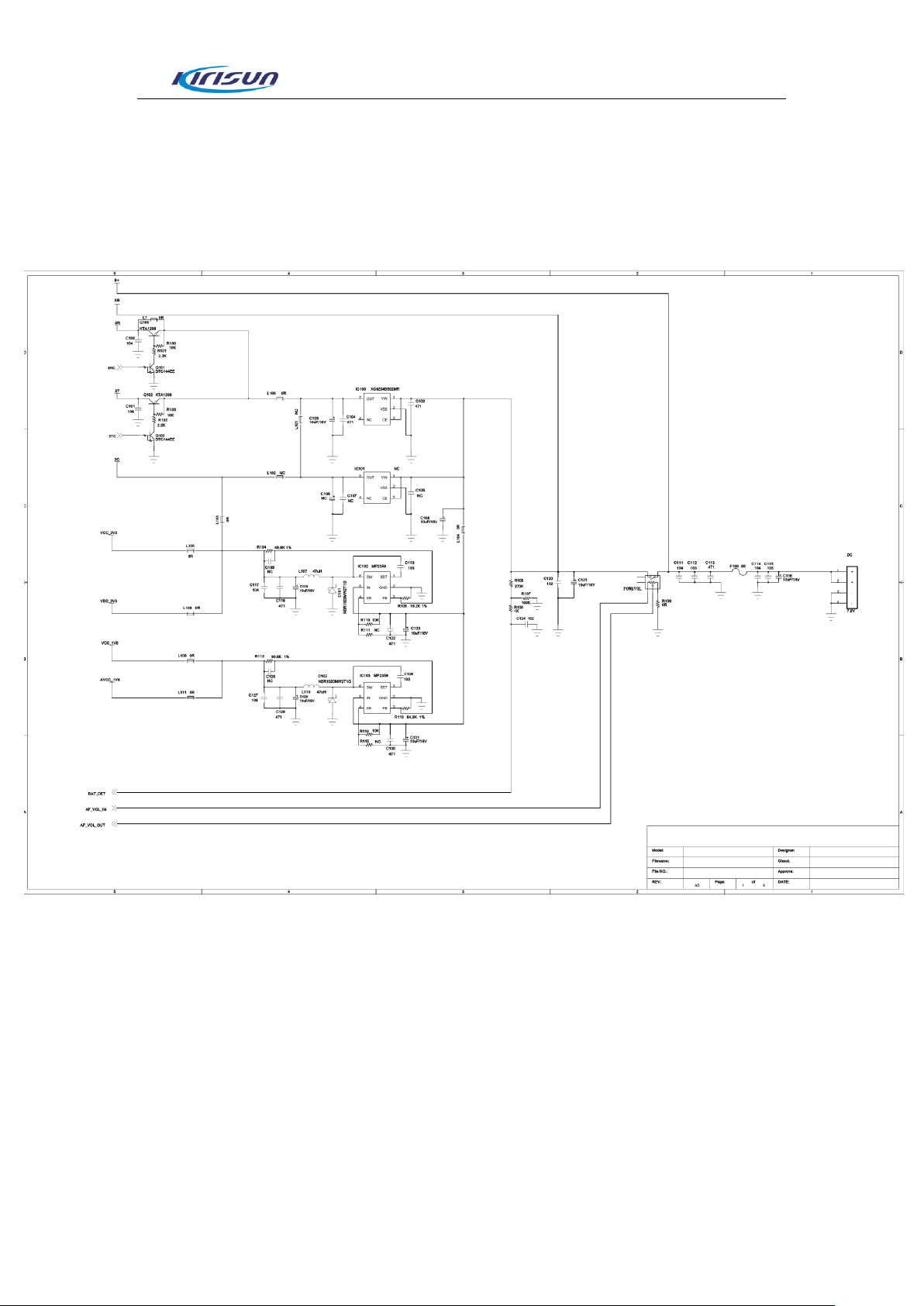
Figure1 FP420 Schematic Pane Diagram
Page 42 of 50
Page 44

FP420 Service Manual
Page 43 of 50
Page 45

FP420 Service Manual
Page 44 of 50
Page 46

FP420 Service Manual
Page 45 of 50
Page 47

FP420 Service Manual
Page 46 of 50
Page 48

FP420 Service Manual
Page 47 of 50
Page 49

FP420 Service Manual
Figure2 FP420 Top Board Position Mark Diagram
Page 48 of 50
Page 50

FP420 Service Manual
Figure3 FP420 Bottom Board Position Mark Diagram
Page 49 of 50
 Loading...