

Page 1
F M540 Serv ice Manual
FM540 㔤؞ሱ䶒
I
Page 2

F M540 Serv ice Manual
Contents
1. Overview ...................................................................................................................................................... 1
1.1. Scope ....................................................................................................................................................................... 1
1.2. Safety Precaution ................................................................................................................................................... 1
2. External Views and Key Features ............................................................................................................. 2
2.1 Front Panel .............................................................................................................................................................. 2
2.2 LCD Display ............................................................................................................................................................ 3
2.3 Rear Panel............................................................................................................................................................... 4
2.4 Microphone (Handheld) ......................................................................................................................................... 4
3. Circuit Description ...................................................................................................................................... 6
3.1 Overview .................................................................................................................................................................. 6
3.2 Frequency Composition of Circuit ........................................................................................................................ 6
3.3 RX Principle ............................................................................................................................................................. 7
3.4 TX Principle ............................................................................................................................................................. 8
3.5 Principle of Frequency Synthesizer ..................................................................................................................... 9
3.6 Audio Processing Circuit ..................................................................................................................................... 10
3.7 Power Supply ........................................................................................................................................................ 10
3.8 MCU Unit ............................................................................................................................................................... 11
3.9 Semiconductor Description ................................................................................................................................. 13
4. Feature Description and Parameter Settings ........................................................................................ 19
4.1 TOT(time-out-timer) ............................................................................................................................................. 19
4.2 Channel Scan ....................................................................................................................................................... 19
4.2.1. Carrier Control Scan ............................................................................................................................ 19
4.2.2. Scan Revert Channel .......................................................................................................................... 20
4.3 Kill and Unkill ......................................................................................................................................................... 20
4.4 Emergency ............................................................................................................................................................ 20
4
.5 Feature and Parameter Settings ........................................................................................................................ 21
5. Assembling and Disassemblin g .............................................................................................................. 22
5.1 Exploded View ...................................................................................................................................................... 22
I
Page 3

F M540 Serv ice Manual
5.2 Maintenance and Disassembling Description .................................................................................................. 24
5.2.1. RF-PCB Disassembling Descript ion ................................................................................................... 24
5.2.2. Key-PCB Disass e mblin g Des cr ipt io n .................................................................................................. 26
6. Test and Modulation ................................................................................................................................. 27
6.1 Test and Modu lat io n M et hod .............................................................................................................................. 27
6.1.1. Parts Required for Modulation............................................................................................................. 27
6.1.2. Manual Modulation .............................................................................................................................. 27
6.1.3. Modulation by Computer ..................................................................................................................... 28
6.2 Radio Test .............................................................................................................................................................. 29
7. Major Technical Performance and Specifications ................................................................................. 30
7.1 General Specifications ......................................................................................................................................... 30
7.2 RX Specification ................................................................................................................................................... 30
7.3 TX Specification .................................................................................................................................................... 31
8. Service and Test Equipment .................................................................................................................... 32
9. Troubleshooting ........................................................................................................................................ 32
Appendix 1 Acrony ms .................................................................................................................................. 34
Appendix2 Material List˄Electrics136-174MHz˅ .................................................................................... 35
Appendix 3 Material Specification(Electronical Parts 400-470) .............................................................. 55
Appendix 4 Material Specification (Stucture) ............................................................................................ 74
Figure 1 FM540-01Mainboard Schem ati c Diagram(136-174MHz) ......................................................... 79
Figure 2 FM540-01 Top Layer Posit i on Diagram(136-174MHz) ............................................................. 86
Figure 3 FM540-01Bottom Layer Position Diagram(136-174MHz) ........................................................ 87
Figure 4 FM540-02 Mainboard Schemati c Diagram( 400-470MHz) ........................................................ 88
Figure 5 FM540-02 Mainboard Top Layer Position Diagram˄400-470MHz˅ ..................................... 95
Figure 6 FM540-02 Mainboar d Bottom Layer Position Diagram˄400-470MHz˅ .............................. 96
Figure 7 FM540 KEY Board Schematic Diagr a m .................................................................................... 97
Figure 8 FM5 4 0KEYTop Layer Position Diagram ................................................................................... 98
Figure 9 FM5 4 0KEY Bottom La yer Position Diagram ............................................................................ 99
II
Page 4

F M540 Serv ice Manual
1. Overview
1.1. Scope
This manual is intended for the maintenance & repair of FM540 and used by engineers and profe ssional
technicians trained by Kirisun. Dada c han ges in thi s manua l may occur w ith th e improv e ment of tec hno logy.
To get the latest t echnology information, please contact us or your local distributor s.
Please read this manual carefully before any maintenance or repair.
1.2. Safety Precaution
Please follow the instructions below to avoid fire or damage to radio:
Maximum continuous working time for transmitingis 1 minute and 4 mniutes for receiving. Long
transmitting or continuous operationon high power mode may cause overheat on the back of the
device.
Do not disassemble the device in any condition.
Do not expose the radio under direct sunlight for long time or put it near any heating device.
Avoid putting the radi o in dusty, humid or water-splashing environment or on uneven surface.
if it is smoking or leaking unusual s m ell, cut off electricity imm ediately and contact local Kirisundealer.
Do not use 24V battery as it is des ign ed to use 13.8V DC power supp ly.
Page 1 of 99
Page 5
F M540 Serv ice Manual
seconds) the button to
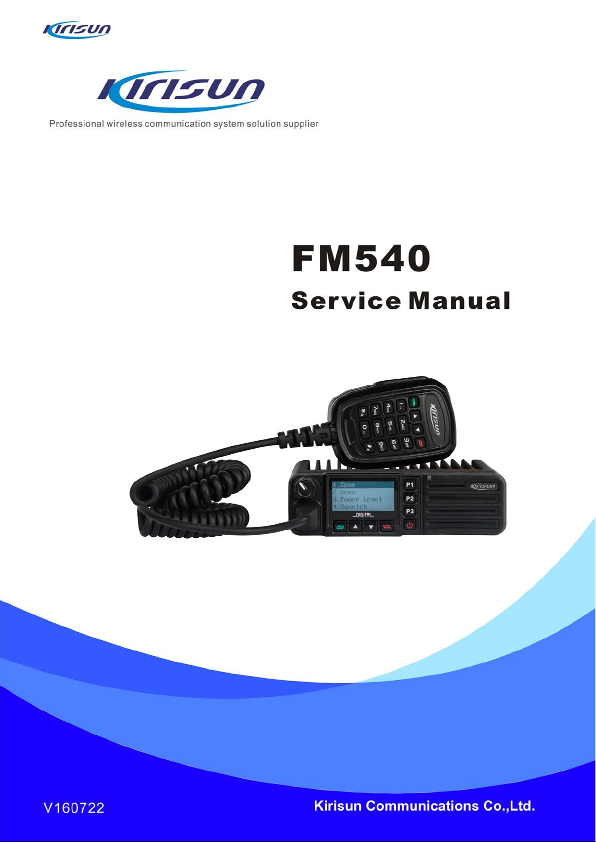
2. External Views and Key Features
2.1 Front Panel
No. Part Name No. Part Name
1 Microphone/Programming Port 2
3
5 P2 Key (programmable key ) 6
LCD Display
4 P1 Key (programmable key )
Refer to “LCD Display” section
Volu me Contro l Knob
Rotate the knob toadjust t he volume
LED Indicator
Red indicator glows: trans m it t ing.
Red indicator flashes: e m er gency,
power-on self-test failure or program
auto upgrade failure.
Green indicator glows: sig nals are being
received or channel activ ities ar e
detected.
Orange indicator flashes: it is in call
hang time (digital).
Green indicator flashes: scanning.
7 Speaker 8 P3 Key (programmable key)
power on/off Butt on
9
11 Down Key 12 Up Key
13 Enter Key
Press (at least 2
power on/off the rad io.
10
Return Key
Press the key to return
Page 2 of 99
Page 6
F M540 Serv ice Manual
2.2 LCD Display
Icon Description
Signal strength indicator. The signal gets stronger with more signal bars.
Unread Message
Full Inbox
The current channel is scanning
High Power
Low Power
Analog Channel
Digital Channel
Emergency state (except secret alarm) or an emergency alarm is received.
Private Call
Group Call
All Call
Transmitting
Receiving
The current digital channel is encrypted
Talkaround
Page 3 of 99
Page 7
F M540 Serv ice Manual
ķĸĹ
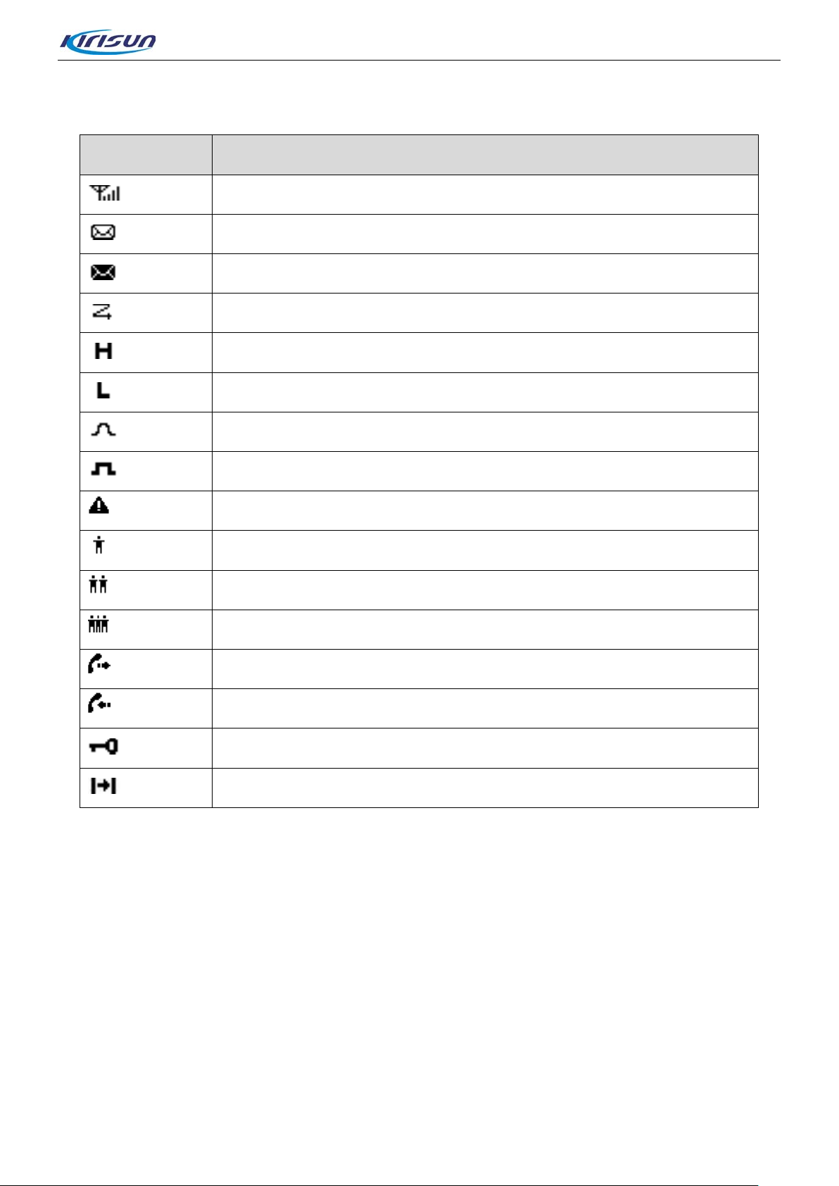
2.3 Rear Panel
No. Part Name No. Part Name
1 Antenna Port 2 Power Port
3 External Speaker Port
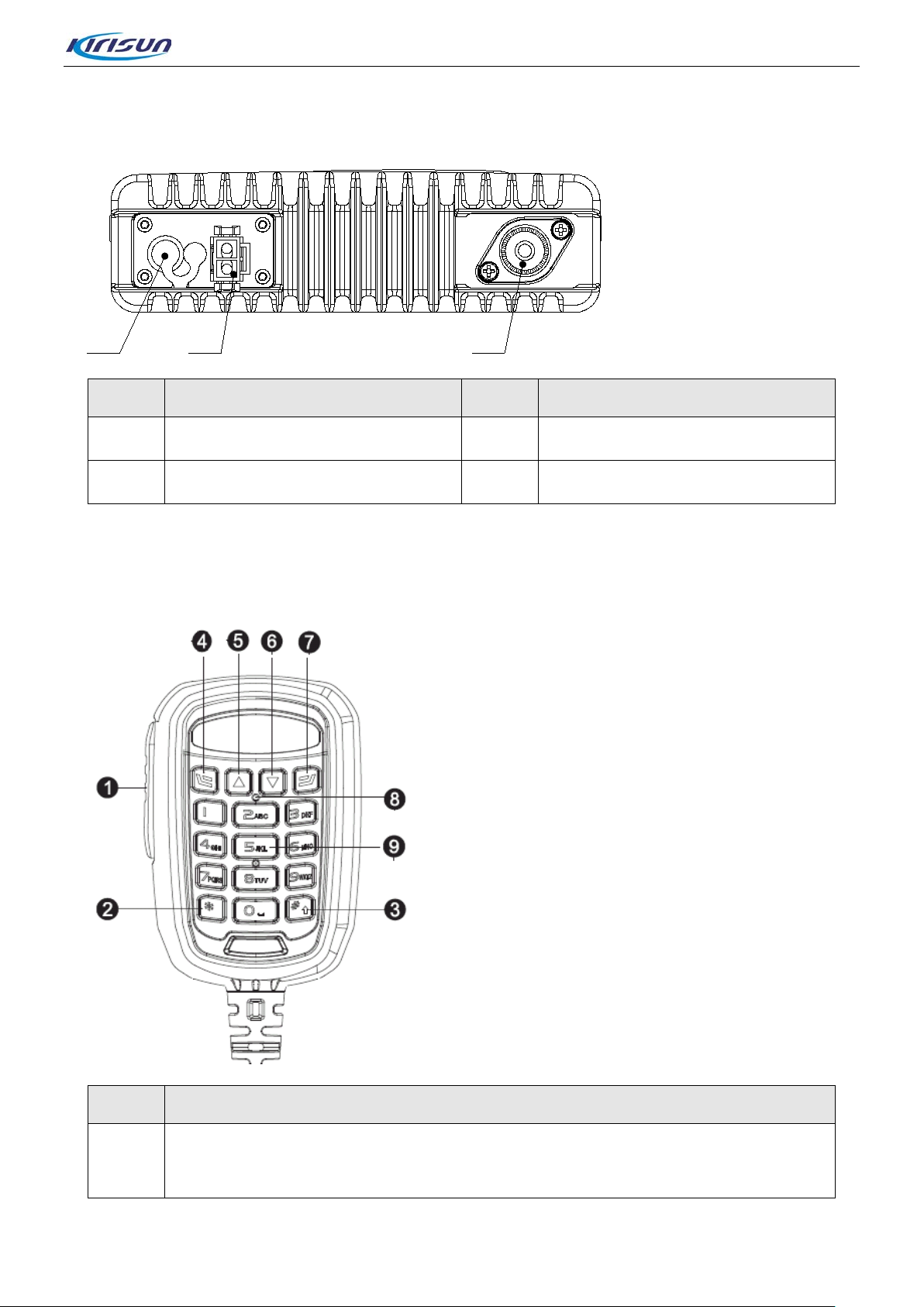
2.4 Microphone (Handheld)
No. Part Name
PTT Key
1
Press the key to transmit and r el ease to receive.
Page 4 of 99
Page 8

F M540 Serv ice Manual
2
3
4
5
6
7
8
* Key
Enter “*”.
# Key
Switch input method.
Enter Key
Programmable key. Set as me nu navigation enter key by default.
Up key
Programmable key. Set as Up K ey by default.
Down Key
Programmable key. Set as Down Key by default.
Return Key
Programmable key. Set as Retur n Key by default.
MIC
Press ǏPTTǐ key and speak to the mic to transmit.
9
Digital Keypad (09)
10 keys in total. Press the key to ent er the number or edit the t ext messa ge or new cont act.
Page 5 of 99
Page 9
F M540 Serv ice Manual
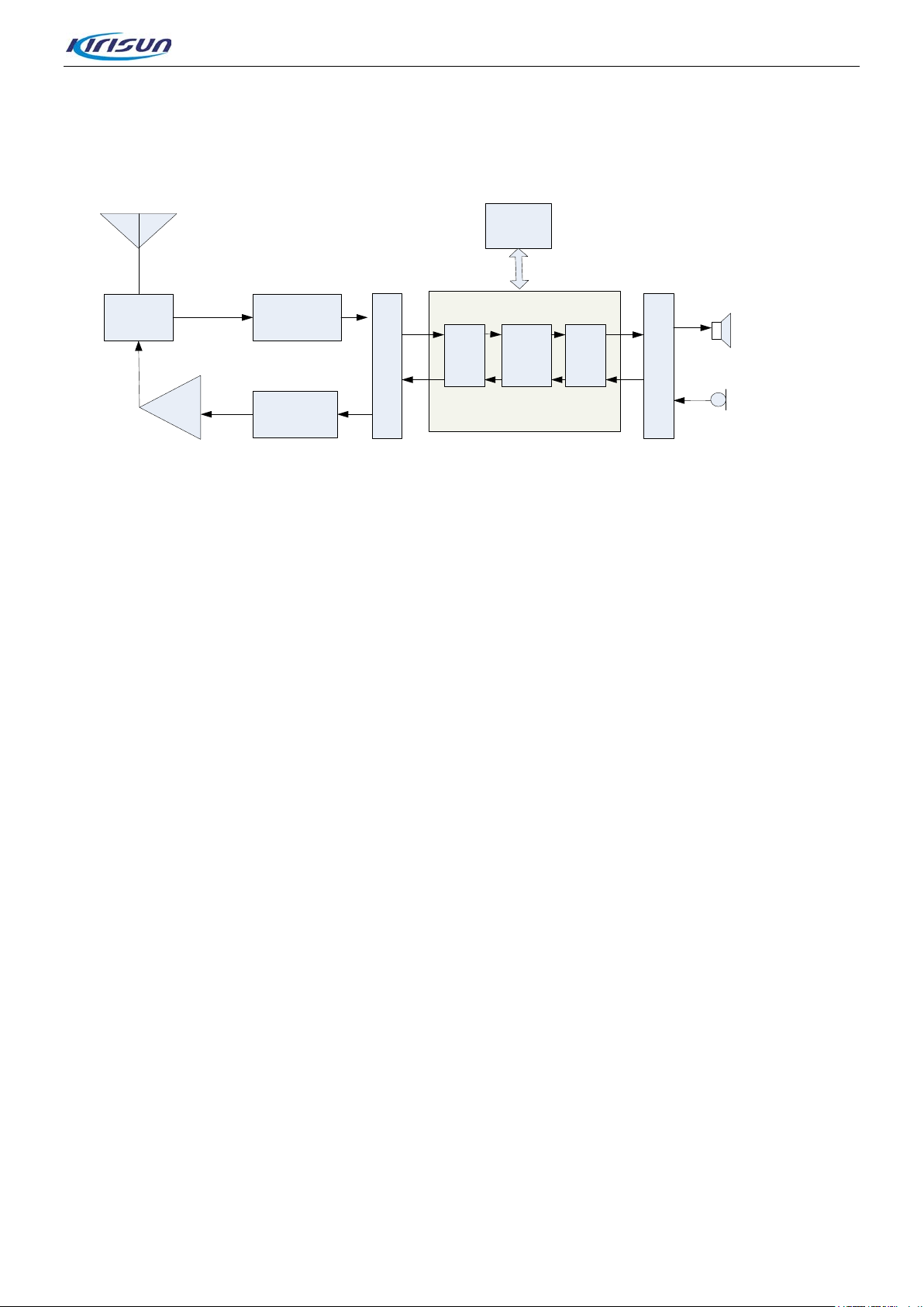
ANT SW
RF
AMP
PA
AMP
TX
AMP
PLL
VCO
IF SYSTEM
X4
multiply
TCXO
12.8MHz
51.65MHz
MCF
CODEC
AF
AMP
MIC
CF
450KHz
ANT
MIXER
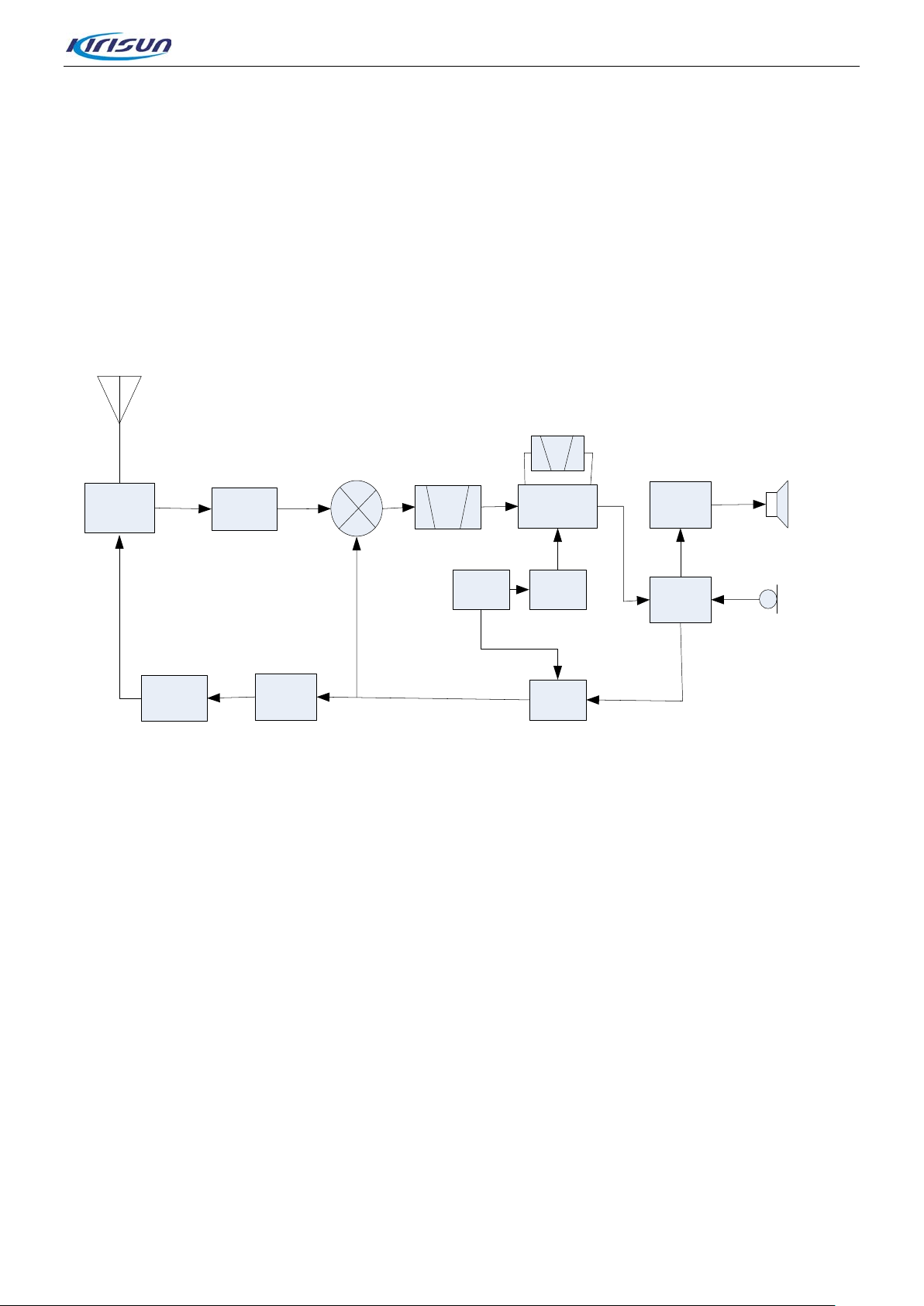
3. Circuit Description
3.1 Overview
This is a FM device.
3.2 Frequency Composi tion of Circuit
Figure 3-1 Circuit Schematic
The receiver applies secondary mixing technology.The first intermediate frequency is 51.65MHz and the
second one is 450 kHz. The first local oscillator is generated by the frequency synt hesizer w hile th e sec on d
one is generated by quadruple frequency of12.8MHz. Txsignal is generated by the frequency synthesizer
and the reference frequen c y of the frequency synthesiz er is generated by TCXO.
Page 6 of 99
Page 10
F M540 Serv ice Manual
ANT SW
BPF
1st local
osc
BPF
MCF
IF AMP
Q20
IF DET
450K
CODEC
AF PA
D3 D37 D36
D11
MIXER
Q19
XF700
51.65MHz
U6IC7
ANT
X1
Multiply
Q11
TCXO
MCU
IC19
PC/TV
Q18
RF AMP
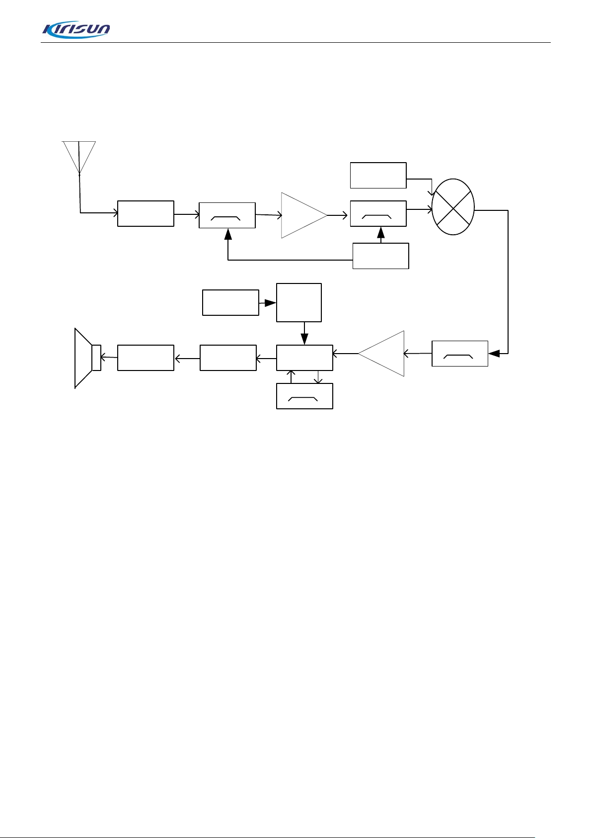
3.3 RX Principle
Figure 3-2 RX Schematic
• Front En d of Receiver
The signal received will passTx-Rx switch controller andalso the BPF composed of LC of two levels
toremove undesired out-of-band signals, then it will be sent to the LNA(low noise amplifier) composed of
Q18 and other peripheral component s for amplif icat ion
The output of LNA passes t he BPF composed of LC of three levels to further remov e undesired out-of-band
signals and is then sent to the first-level fre quency mixer Q19.
• The First Mixer
The signal from LNA mixes with the first local oscillator signal from the frequency synthesizer to generate
the first intermediate frequ enc y (51.65MHz) signal.
• IF Circuit
The first IF signal passes t he cry stal filter (XF700) to remove the sign als fro m t he adjac ent chan ne l or other
channels.
The first IF signal from the crystal filter is sent to the IF- processing IC(IC6, GT3136) after bei ng am plif ied
by the first IF amplifier (Q20).
IF IC includes secondary mixer, IF amplifier, limiter, frequency detector, noise amplifier and audio low pass
filter.
The 12.8MHz signal from X1 passes Q300 and the peripheral circuit for amplification and then the second
local oscillator of 51.2MHz is acquired. The second oscillator (51.2MHz) mixes frequency with the first IF
Page 7 of 99
Page 11
F M540 Serv ice Manual
8T
SW
D2
DRIVE AMP
Q5
FINAL AMP
IC1
ANT SW
D3,D37
LPF
APC
IC4
APC
8T
8T
8T
D9,D10
RX BPF
VGG
VSWR
signal (51.65MHz) in IC6 to gener ate the second IF signal (450kHz). The second IF signal will be amplified
and limited in IC700 and after being filtered by CF1 crystal filter (450kHz), it will be demodulated by IC700
and audio signal will be output .
• Squelch Circuit
The signal demodulated by IC6 is sent to the noise amplifier, and the amplified noise signal is sent to Q21
for further amplification and to D21 for wave detection to generate DC electric level, which is sent to the
MCU control squelch circuit. The voltage is inversely proportional to the input sign al.
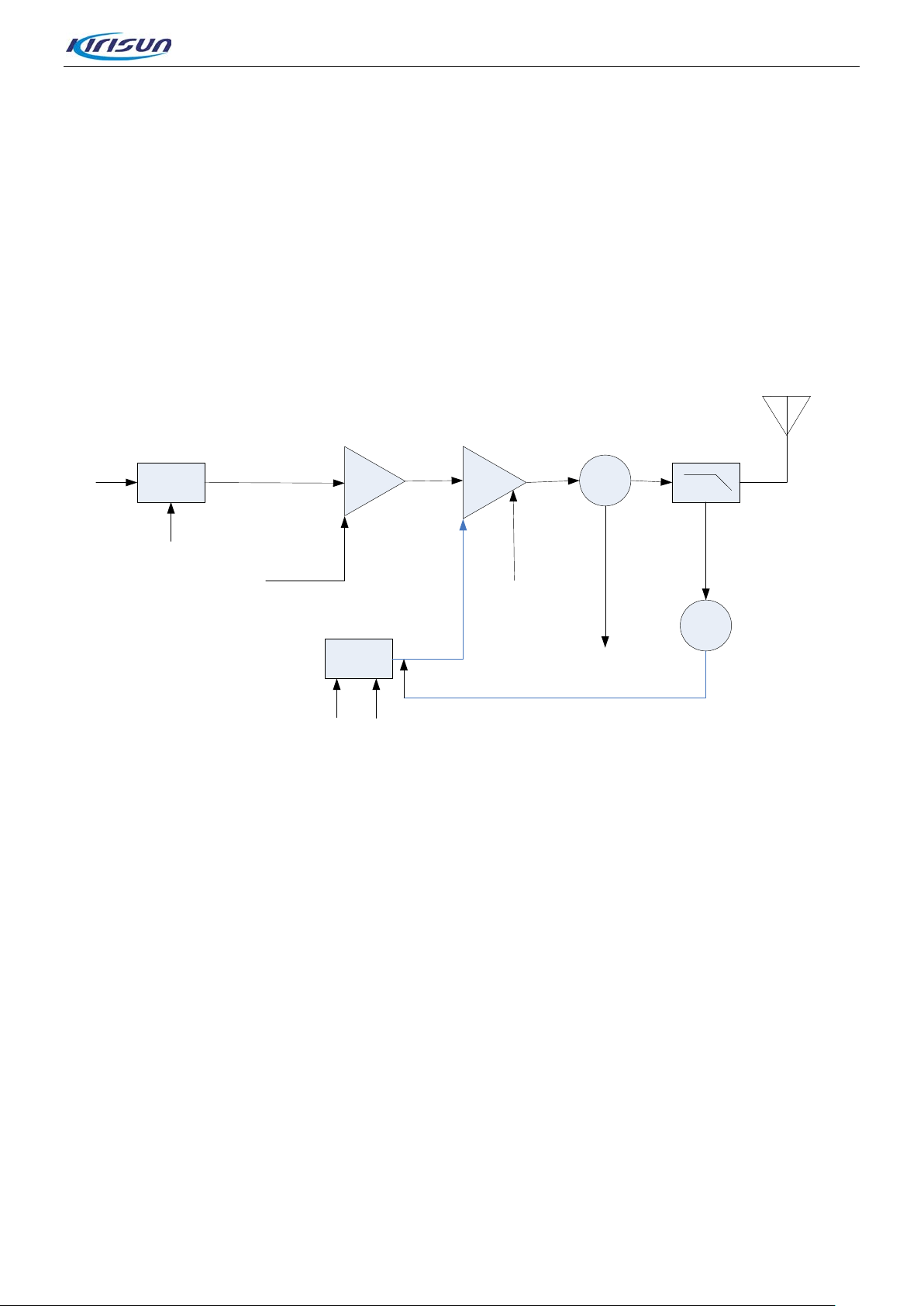
3.4 TX Principle
Figure 3-3 Power Ampl ification and Antenna Schematic Diagram
The modulated RF sig nal from VCO is sent to Q600 for power ampli fication a fter bein g amplif ied by Q1, Q2,
and Q5.
IC4 is controlled by MCU APC circuit to change the grid bias voltage, easily controlling the output power of
the transmitter.
• APC (automatic power control) Circuit
D9 and D10 are standing w ave current detection. IC4 is power amplifier.
If the output power of the transmitter is too high, the power amplifier current increases and the output
voltage from D9 and D10 will go up, which causes the VGG offset voltage on IC1 decreases and thus the
output power of the transm itter decreas es. Vice versa. In this way, the output power of the transmitter stays
stable in different working environ ment.
MCU sets the power by changing the voltage input to IC4.
Page 8 of 99
Page 12
F M540 Serv ice Manual
15
PLL
DATA
LPF
Q12
RX VCO
PLL
DATA
Q1
BUFF AMP
12.8MHz
TCXO
X1
IC3
PLL IC
Q6
TX VCO
Q25,U2
SW
Q2
RF AMP
LPF
MCU
IC12
½ FREQ
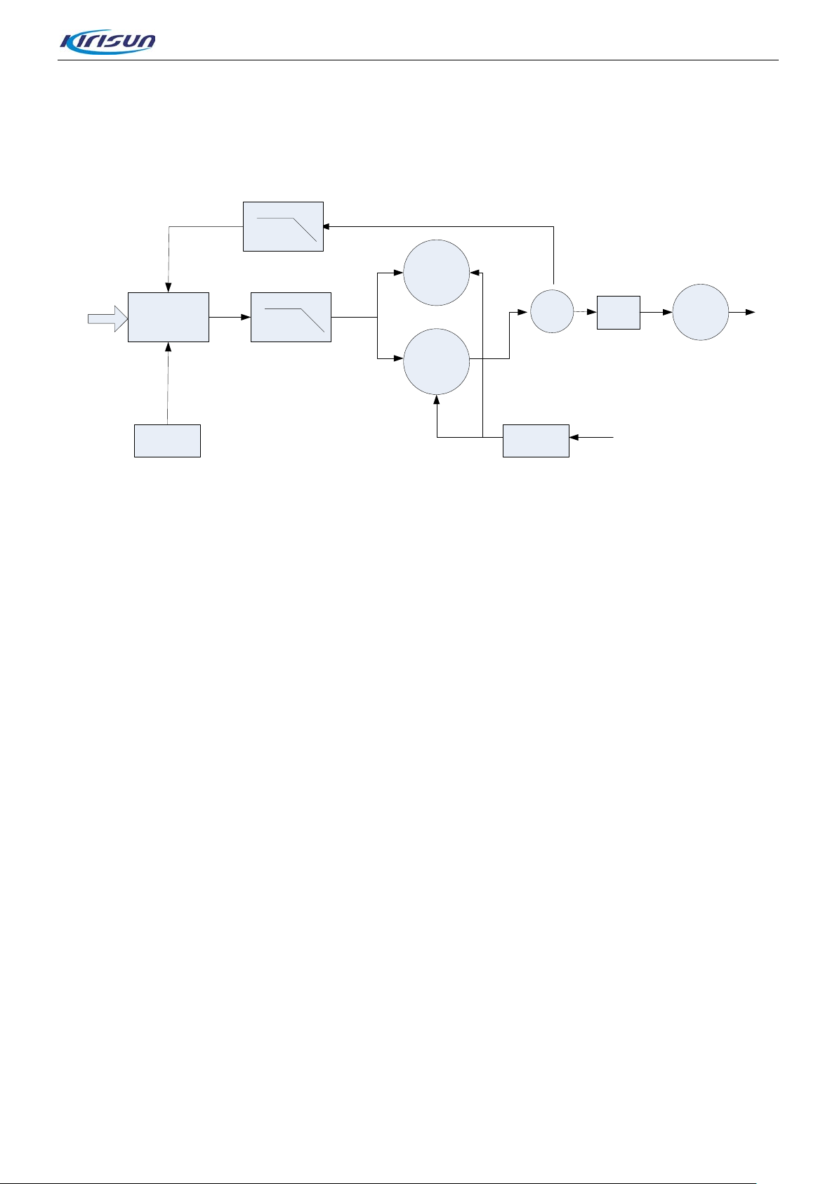
3.5 Principle of Frequency Synthesiz er
Figure 3-4Diagram of Frequency Synthesizer
This radio applies PLL frequency synthesizer.The frequency synthesizer consists of reference oscillator,
voltage controlled osc il lator (VCO), programmable f r equency divider, phase comparator and low pass filter.
Q6, D1, D4, D5, D6 and other resistor-capacitor components compose TX VCO unit. D8 is the modulation
circuit of TX VCO.
Q12, D4, D16, D17, D18 and other resistor capacitor components compose RX VCO unit.
IC3 (MB15E03) is PLL i ntegrated circuit, which contains programmable reference divider, programmable
divider, phase comparator, charge pump and so on. R54, C113, R55, R57, C117, R51, C109 an d so on
compose loop filter.
The reference frequency is offered by X1 (TCXO, 12.8MHz).
The reference frequency from TCXO(temperature controlled crystal oscillator) is divided by the
programmable reference divider in IC3 to generate reference frequency of 5kHz or 6.25kHz(based on the
set channel frequency and cont r ol led by MCU).
The oscillation frequency f rom VCO is sent to IC3 after bei ng mu ltipli ed by s econd multip lier circ uit, and will
then be compared to reference frequency after being divided by programmable divider to get error signal.
The error signal will be filtered by the low pass filter and sent to VCO to change the oscillation frequency.
When the VCO frequency r eaches the set value, VCO is locked.
Loss of Lock Detection: when PLL loses its lock, IC3 pin1 4 outputs low electric level signal to MCU and
MCU controls the transmitter to forbid the transmitting and sound alert. When locked, IC3 pin14 outputs
high electric level.
Page 9 of 99
Page 13
F M540 Serv ice Manual
FM receiver
FM modulatorPA
TR
SW
Host MCU
4
FSK
Protocol
stack
Voice
coder
U6 CODECL
U6 CODECR
ANT
SCT3252
U1
IC2
SPK
MIC
3.6 Audio Processing Circuit
Figure 3-5 Frequency Synthesis Diagram
• MIC Signal Processing
The audio signal from MIC is sent to U6 for A/D audio switch and sent to U1 SCT3252 for internal adio
encoding/decoding, communication protocol processing, channel coding modulation. Afterwards, MOD2,
MOD1 are output through tw o separate pat hs fr om U6 and sent separately to TCXO and VCO for two-point
modulation. 4FSK modulation signal is output in digital status and sine wave signal is output in analog
status.
• RX Audio Signal Pr ocessing
The audio signal demodulated from IC700 is sen t t o U6 for A/D audio switch and then be processed by U1
SCT3252. After audio pro cess ing, co mmu nicatio n prot ocol proc ess ing and D SP, the signal is sent to U6 for
D/A switch and output to audio power deviceU800(TDA2822) for amplification, motivating the speaker to
sound.
Squelch Circuit: demodula ted and output byIC700; it passes filter circuit and the nois e will be remov ed from
demodulated signal and amplified by Q700; after detection by D701, it will be sent to MCU. MCU identifies
the noise volume and controls the squelch.
Speaker Impedance: 16Ω.
Notes:
• Any terminal of the speak er mu st not be attached to the ground!
• The emergency alert tone is not controlled by volume.
3.7 Power Supply
This radio applies 13.8V battery. The transmitter power amplifier circuit (IC1) and the receiver audio
processor (IC7) directly use the battery for power supply with other circuits using 5V for power supply.
Q38: 8T switch; controll ed by MCU. 8T supplies power for t he t r ansmitter front end.
Q40: 8R switch; controlled by MCU. 8R supplies power for receiver RF amplifier, mixer, IF processor, and
other units.
Page 10 of 99
Page 14

F M540 Serv ice Manual
IC1: 5C switch. 5V circuit is controlled by MCU. 5C supp lies power for frequency sy nt hes iz er.
IC8, IC102: 3V and 1.2V DC\DC voltage stabilizing circuit; supplies DC current for U1 (SCT3252F).
IC9: 8V three-terminal volt age st abilizing circuit.
3.8 MCU Unit
MCU unit
MCU unit controls the operation of eac h unit and realizes all the features on the device:
• Communication with PC
• Saves the status data
• Control PLL to generate RX/ TX local oscillation frequency
• Acquire s t he c ur rent channel status
• Controls LED status indication
• Controls power supply of each unit
• Chec k action from each feature key
• Generates CTCSS signal
• GneratesDCS signal
• Generates power control signal
• Completes CTCSS decoding
• Completes DCS decoding
• Squelch detection and control
• Control t he content of voice prompt
Memorizer (E2PROMˈAT24LC512BN)
It stores channel data, CTCSS/DCS data, feature configuration data and para meter adjustment data.
CTCSS/DCS Signal Encoding and Decoding
The CTCSS/DCS signal generated by MCU is sent s eparately to VCO and TCXO for modulation.
The CTCSS/DCS signal from the receiver is sent to MCU for decoding. MCU will try to identify the
CTCSS/DCS signal received which is the same as the device and the speaker will be turned on if it does.
CTCSS
CTCSS (continuous ton e contr ol squ elch s yst em) is a sque lch cont ro l syst e m modulated on the car rier wit h
the CTCSS signal being the pilot frequency
If the CTCSS feature is set, the conversat ion is enabled on ly w hen the CTCSS frequency from the receiv er
and transmitter is the same t o avoid interference from other sign al s .
Page 11 of 99
Page 15
F M540 Serv ice Manual
39 groups of standard CT CS S fr equency of this radio are available. See Chart 1.
CTCSS signal is generated by MCU (PWM wave form), and it is sent to VCO for modulation after being
filtered by the low pass filter composed o f RC for eliminating the frequency hi gher t han 300Hz.
Chart 3-1 CTCSS Frequency Chart
No. Frequency [Hz] No. Frequency [Hz] No. Frequency [Hz] No. Frequency [Hz]
1 67.0 11 94.8 21 131.8 31 186.2
2 69.3 12 97.4 22 136.5 32 192.8
3 71.9 13 100.0 23 141.3 33 203.5
4 74.4 14 103.5 24 146.2 34 210.7
5 77.0 15 107.2 25 151.4 35 218.1
6 79.7 16 110.9 26 156.7 36 225.7
7 82.5 17 114.8 27 162.2 37 233.6
8 85.4 18 118.8 28 167.9 38 241.8
9 88.5 19 123.0 29 173.8 39 250.3
10 91.5 20 127.3 30 179.9
DCS Signal
DCS (digital code squelch) is a continuo us numeri cal code w hich is modu lated along w ith the speec h sign al
on the carrier to control the squelch. If the DCS feature is set, the speaker is on only when the same DCS
code is received to avoid the unn ecessary signal interference.
83 kinds of standard code of this radio are available. See chart 3-2.
DCS signal is generated by MCU (PWM wave form), and it is sent to VCO and TCXO for modulation after
being filtered by the low pass filter composed of RC for eliminating the frequency higher than 300Hz. VCO
modulates the high freque ncy of DCS signal and TCX O modu lat es the low frequency of DCS signal.
CTCSS/DCS signal from t he receiver is sent t o MCU for dec od ing. MCU will try to identify the CTCSS/DCS
signal received which is the same as the device and the speaker will be tur ned on if it does.
Chart 3-2 DCS Encoding Chart
023 114 174 315 445 631
025 115 205 331 464 632
Page 12 of 99
Page 16
F M540 Serv ice Manual
026 116 223 343 465 654
031 125 226 346 466 662
032 131 243 351 503 664
043 132 244 364 506 703
047 134 245 365 516 712
051 143 251 371 532 723
054 152 261 411 546 731
065 155 263 412 565 732
071 156 265 413 606 734
072 162 271 423 612 743
073 165 306 431 624 754
074 172 311 432 627
3.9 Semiconductor Description
Chart 3-3 Microprocessor (M30620) Port Descri ption
Pin No. Port Name Input/ output Function
1 VCCN D/A Output Reference frequency ad justment output
2 TONE_OUT D/A Output DTMF/Tone output, beep output
3 HSDI I Tone decodin g in put
4 EPDT I/O EEPROM data input / out put
5 EPCK O EEPROM clock
6 BYTE I GND
7 CNVSS I GND
8 BSHIFT O Clock beat frequency control
9 SV O Min. volume control
10 RESET I CPU reset input
Page 13 of 99
Page 17

F M540 Serv ice Manual
11 XOUT O CPU clock output
12 VSS - GND
13 XIN I CPU clo c k inp ut
14 VCC - +5V
15 NC I +5V
16 PTT I PTT key
17 RD NC I NC
18 NC I NC
19 NC O NC
20 NC I/O NC
21 NC O NC
22 S_CS O FLASH data output
23 S_SO I FLASHdata output
24 NC O NC
25 S_SCK O FLASH data output
26 PC/TV O TX power,receving frequency band voltage tunning
27 S_SI - FLASH data output
28 NC O NC
29 TXD O TXD1 output
30 RXD I RXD1 input
31 C_CLK - Emulator interface
32 C_BUSY O Emulator interface
33 TXD0 O NC
34 RXD0 I NC
35 AFCO_1 O RX/TX audio power amplification control pin
36 NC O NC
Page 14 of 99
Page 18

F M540 Serv ice Manual
37 RX SW O Receiver VCO switch
38 TX SW O Transmitter VCO switch
39 C_CE - Emulator interface
40 PLL UL I Phase-locked loop loss of lock check pin
41 PLL ST D O Phase-locked loop enabling control
42 PLL DATA O Phase-locked loop data output
43 PLL CLK O Phase-locked loop clock
44 NC - NC
45 SCT3252MOD O Data output pin
46 GREEN_LED I RX status indicator
47 RED_LED I TX status indicator
48 8TC I 8T control pin
49 8RC I 8R control pin
50 SBC I SB control p in
51 INTO O Baseband wake-up pin
52 PLLBYOPASS O Baseband bypass pin
53 PLLSEL2 O PLLHigh/low Selection
54 HCSN O Baseband Chip Selection
55 HWRN I Baseband data writing enable
56 HRDN O Baseband data reading enable
57 HOBIB O Baseband data check
58 RSTN_3252 O Baseband reset
59 NMI - Baseband wake-up foot
60 ACC - +5V
61 PIO3 - Baseband wake-up foot
62 VSS - GND
Page 15 of 99
Page 19
F M540 Serv ice Manual
63 HPI_DATA0 - HPI address bus
64 HPI_DATA1 - HPI ad dress bus
65 HPI_DATA2 I HPI address bus
66 HPI_DATA3 I HPI address bus
67 HPI_DATA4 I HPI address bus
68 HPI_DATA5 I/O HPI address bus
69 HPI_DATA6 I/O HPI address bus
70 HPI_DATA7 I/O HPI address bus
71 SI/D7 I LCD data output
72 SCL/D6 I LCD data output
73 A0 I L LCD data output
74 /RST I LCD reset pin
75 /CS1 I LCD data output
76 NC O NC
77 NC O NC
78 BASEBAND_C O Baseband power control pin
79 D0 O DTMF data pin
80 D1 O DTMF data pin
81 D2 O DTMF data pin
82 D3 O DTMF data pin
83 DV O DTMF data pin
84 NC O NC
85 NC O NC
86 HOOK - HOOK control pin
87 BEEP_C I Reverse detection input
88 BATT I Voltage check input
Page 16 of 99
Page 20
F M540 Serv ice Manual
local oscillator, second IF amplification,
89 RSSI I Receiving filed intensit y signal input
90 BUSY I Squelch voltage check input
91 VOL_DET I VOL_DET
92 PF2 I PF2
93 PF1 I PF1
94 AVSS - GND
95 TEMP - TX temperature detection
96 VREF - +5V
97 AVCC - +5V
98 W/N - W/N switch pin
99 MD I Speaker micdata input pin
100 TGSW O TX control pin
Chart 3-4 Semiconductor Descript ion
Position Mark Model Feature Description
IC202 PST9140NR MCU reset circuit
IC3 MB15E03 Frequency synthesizer
IC4 NJM2904 APC, volatage comparison, driv er
Receiver second
IC6 GT3136
amplitude limiting, demo dulation, noise amplification.
IC204 NJM2902 Receiver demodulation signal amplification and filtering.
IC1 M30620 MCU
E2PROM, stores channel frequency dat a, feature settings and
IC200 AT24C512C
modulation status para me ters.
IC7 TDA1519C Receiver audio power ampli f ication
Q12 2SC3356 RX VCO oscillator tube
Q1 2SC5108 VCO buffer amplifier
Page 17 of 99
Page 21
F M540 Serv ice Manual
U2 UMC4 TX VCO control switch
Q7 2SC5108 Feedback loop amplifier
Q25 DTA143TE RX VCO control switch
Q14 2SC4617 VCO power filter
Q2 2SC5108 VCO buffer amplifier
Q11 2SC5108 RX second local oscillation am plifier
Q6 2SC3356 TX VCO oscillation tube
Q5 2SC3357 Trasmitter power a mp li f ication boost
IC1 RA30H1317M Transmission level final power amplification
Q4 2SC3357 Transmitter 1st amplification
Q18 3SK318 Receiver low noise amplification
Q19 3SK318 1st level mixer
Q20 2SC5108 First IF amplifier
Q21 2SC4617 Receiver noise amplifier
Q22 FMMT717 Audio output control switch
Q23 DTC144EE Audio power amplification control switch
IC9 L7808CV 8V three-terminal regulated output
IC11 XC6204B502MR Adjustable 5C regulated output
Q40 KTA1298 Adjustable 8R regulated output
Q38 KTA1298 Adjustable 8T regulated output
IC102 XC6228D122VR 1.8Vvoltage output modulation
IC2 TA78033AF 3Mvoltage output modulation
Chart 3-5 Diode Description
Position Mark Model Feature Descript i on
D12 DA2S10100L Diode for loss of lock detect ion
D8 1SV278 TX VCO modulati on diode
Page 18 of 99
Page 22

D1,D4
D5,D6
F M540 Serv ice Manual
1SV305 TX VCO oscillation varactor
D14,D15D16,D
17
D19 HSC277 RX VCO output switch diode
D2 HSC277 TX VCO output switch diode
D7 HZU5ALL APC output voltage-limiting diode
D3,D37
D36
D27,D28,D29,D
30
D25 RB706F Commutation diode
1SV305 RX VCO oscillation varactor
HVC131 Transmitter antenna switc h dio de
1SV305 RX band pass filter varactor
4. Feature Description and Parameter Settings
4.1 TOT(time-out-timer)
This feature prevents the user from long occupation of the channel. If the transmitting period exceeds the
dealer’s preprogrammed time, the radio stops transmitting and rings alert tone. To stop the alert tone,
please release the PTT button. For a second transmission, please press the PTT button after a certain
period (set by the dealer). If the dealer preprograms the pre-warning feature, a warning is given when the
transmitting period gets c l ose to its time-out-timer limit, indicating the transmission will be forbidden soon.
4.2 Channel Scan
Channel Scan is able to search for the channel where there is a signal, and the radio stays on the channel
where a signal is detected to make a conversation. The scan method is carrier control scan.
4.2.1. Carrier Control Scan
The radio scan stays on a busy channel until it is no longer busy, and the scan is enabled automatically
after a certain period (the specific period time is set by the local dealer).
Press the “Scan” shortcut key, and the radio scans the scan list of the current channel. When the radio is
scanning, you can press t he “ Scan” shortcut key to stop scanning.
Page 19 of 99
Page 23

F M540 Serv ice Manual
4.2.2. Scan Revert Channel
When the radio is scanning, press the PTT button” and the radio transmits and communicates on a preset
channel. This channel can be program m ed by the local distributor.
4.3 Kill and Unkill
If the dealer enables this feature, the radio can receive and decode other radio’s signals of Kill and Unkill
before responding accordingly. After being killed, the radio can only receive the activated signal without
being able to transmit or receive other signals. The radio is back to normal after activation.
4.4 Emergency
In a state of emergency, press the “Emergency On” shortcut key for the alarm call. The alarm method is
composed of two parts: Alarm type, which mainly specifies the acoustooptic reaction in the state of alarm
call; Alarm mode, which specifies the sending content in the state of alarm call. These parameters can be
set by the dealer to meet your requirements. To disable the emergency feature, please press the
“Emergency Off” shor t cut key.
Alarm Type
• None: no alarm feature (by default), and the alarm cannot be initiated by pr essing the e mergency but ton.
• Siren Only: the radio only sounds siren locally.
• Regular: acoustooptic alert for alarm status, able to receive response fro m other members.
• Secret: no acoustooptic alert for alarm and do not receive response from members.
• Secret w ith Voice: no acoustooptic alert for alarm but receives response from other members.
Alarm Mode
• Emergency Alarm: after the alarm is initiated, the radio only transmits emer gency alarm, and
afterwards,it automatic exitsalarm status.
• Emergency Alarm + Emergency C all: the rad io trans mits emer gency a larm an d sends out emergency call
by pressing the PTT but ton.
• Emergency Alarm + Auto T rans mission of Background Tone: the radio transmits emergency alarm, and
the background tone will be sent out per iodically and automatically in the way of emergency call.
Note:
• Emergency Alarm: a non-speech s ignal is transmitt ed by the mobile radio to trigger other radios to
send out an alert.
• Emergency Call: a call mode with the priority of using channe lsso as to ensure smooth call during
emergency.
Page 20 of 99
Page 24
F M540 Serv ice Manual
4.5 Feature and Parameter Settings
The radio is preset before the factory delivery, but the settings of digit al feature s, operational frequency,
channel, QT/DQT, and auto scan feature amy be reset according to different requirements.Therefore,
Kirisunspecifically designed Chinese/English FM540 programming software with friendly interface, easy
operation and clear visual disp lay to help complete parameter set tings for FM540.
The stepsof setting parameters with computer are as below:
Step 1.Install FM540 programmin g software on the computer.
Step 2. Use FM540 programming cable to connect the radio to PC serial port. See the following:
Note: please turn off the radio be fore connection.
Computer FM540 prgramming cable Mobile Radio
Step 3. Turn on t he mobile radio.
Step 4.Click to operateFM540 programming so ftware program.
Step 5.Click “Read” in the main menu of FM540 programming software to read the radio parameters into
PC.
For detailed operation,please refer to the help file in FM540 programming software and the instruction
manual.
Page 21 of 99
Page 25
F M540 Serv ice Manual
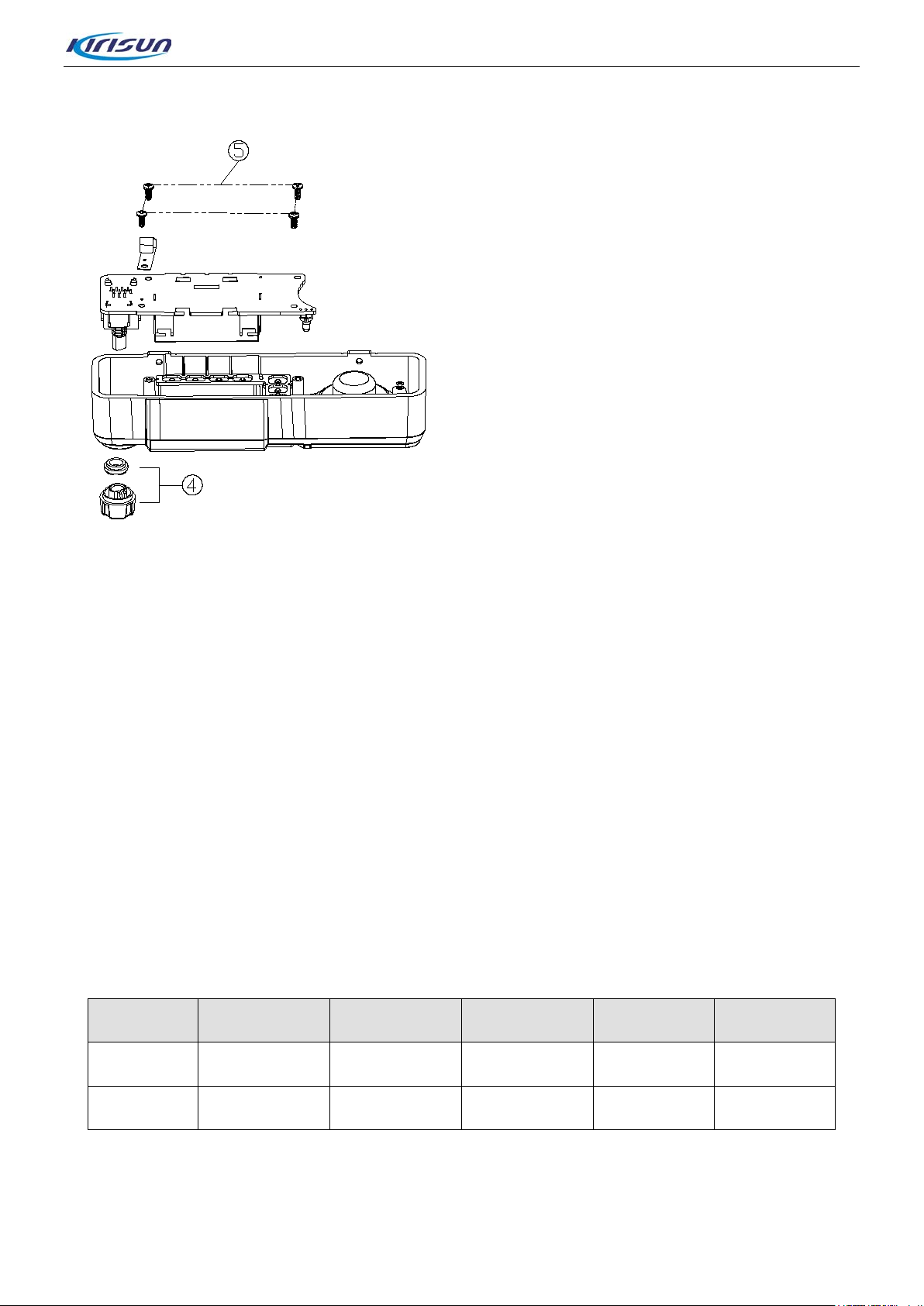
&$6()5217$66(0%/<
5. Assembling and Disassembling
This radio is sophisticated communication equipment with a precise and compact mechanism. The
assembly and disassembly of the radio must be car efully performed during t he repair. The description is as
follows:
5.1 Exploded View
No. Part No. Description Quantity
1 7WFP-4090-01A FM540lens protective film 1
2 7MBP-4090-02A-WC FM540 LCD film 1
Page 22 of 99
Page 26
F M540 Serv ice Manual
3 7MHJ-4090-01A-W FM540 lens double-sided adhesive 1
4 7SMF-025050M-MHYB-B M2.5*5 flat round torx-head machine screw 2
5 7MBP-4090-03A-WC FM540 light pipe 1
6 7PLJ-4028-E02A KME-221 brand sticker 1
7 7MBP-4090-01A-W0 FM540 front shell 1
8 7MHR-1939-03A-W0 PT8000 speaker dust-proof net 1
9 4SS7-3520-016-700 Speaker 1
10 3WPT-S1938-01A Black and white twisted pair 1
11 3WF7-05034-060C4 Flexible connecting cab le 1
12 7MHR-1939-04A-W1 PT8000 front panel upper gasket 1
13 7MHR-1939-04A-W0 PT8000 front panel upper gasket 1
14 7MHL-1939-01C-L0 PT8000 alu m in um alloy top cover 1
15 3WPD-S7038-B PT8000/8100 power connecting cable 1
16 7MBP-7038-03A-W0 PT8100 power cable clip 1
17 7MHF-1939-01A-L0 PT8000 metal plate 1
18 7MHR-1943-02A-W0 PT8200speaker hole plug 1
19 7SAF-030100M-SZYB-N1 Screw M3*10 with spring washer 5
20 3CR7-S1943-B PT8200 anten na head 1
21 1MR3-RA30H4047M Power module 1
22 7MMC-1943-01A-N PT8200 power module shield ing cover 1
23 7MBM-S1943-B PT8200 conductive foam 1
24 6SS2-4090-BMA FM540 mainboard suite 1
25 7SMF-030060M-SZYB-N Screw M3*6 5
26 7MHR-1939-04A-W2 PT8000 aluminum gasket 2
27 7MHL-1939-02C-L0 PT8000 alu m in um ally bottom cover 1
Page 23 of 99
Page 27
F M540 Serv ice Manual
28 7SMF-030250-SZYB-N Screw M3*25 6
29 7MBP-7038-02A-W0A PT8100 volume knob 1
30 7NRC-077107040-Z Channel knob nut 1
31 7MBP-4090-04A-W0 FM540 menu key 1
32 7MBP-4090-05A-W0 FM540 top selection key 1
33 7MBP-4090-06A-W0 FM540 bottom selection key 1
34 7MBP-4090-07A-W0 FM540 return key 1
35 7MBP-4090-08A-W0 FM540 feature key P1 1
36 7MBP-4090-09A-W0 FM540 feature key P2 1
37 7MBP-4090-10A-W0 FM540 feature keyP3 1
38 7MBP-4090-11A-W0 FM540 power key 1
39 7MBR-4090-01A-W0 FM540 silicone key 1
40 7GCM-508305-J FM540 LCD foam cushion 1
41 4PC7-4090H-A FM540 LCD module 1
42 7MHS-4090-02A-W FM540 LCD bracket 1
43 7MHS-4090-01A-J FM540 metal dome key 1
44 6SS2-4090-HKA FM540 keyboard suite 1
45 7MHS-4090-02A-W FM540 key PCB grounding spring 1
46 7STF-026060B-SZYB-Z Screw M2.6*6 4
5.2 Maintenance and Disassembling Description
5.2.1. RF-PCB Disassembling Description
Step 1. Unscrew the six M3*25 screws on the top and bottom cover,as shown in ķ,open the aluminum
bottomcover ( see the figur e below ).
Step 2. Loose thetwo power amplification module screws as shown in ĸ. Disassemble the power module
shieldi ng case, and use the soldering iron to separate the pins of the power amplification module from
Page 24 of 99
Page 28
F M540 Serv ice Manual
PCB(see the figure below ).
Step 3. Loose the four M2.5*5 panel screws as shown in Ĺ. Disassemble the metal panel,plastic
buckleand speaker plug ( see the picture below).
Step 4.Unplug the flat cable and speaker cable, and use the soldering iron to separate the antenna head
from RF-PCB; loosen the screw and carefully remove RF-PCB from the top aluminum cover. (seethe
picture shown below).
Page 25 of 99
Page 29
F M540 Serv ice Manual
5.2.2. Key-PCB Disassembling Description
Step 1. loose the six 6 M3*25 screws on the top and bottom cover as show n in ķ, and open the alu min u m
bottom cover (see the figu r e show n below).
Step 2. remove the flat cable a nd s peaker cable from the mainboard a s shown in ĸ.
Step 3. remove the two M2.5*5 panel screws as shown in Ĺ, and separate th e panel from the main unit.
Step 4. remove the volume knob and take off the circlipon the knob as well as the the switchnut as shown
in ĺ.
Step 5. remove the four M2.6*6 KEY-PCB fixed screws as shown in Ļ and remove KEY-PCB from the
Page 26 of 99
Page 30
F M540 Serv ice Manual
plastic panel.(seethe figure shown below).
After the disassembly, you can perform further repair and m odulation based on faults.
6. Test and Modulation
6.1 Test and Modulation Method
During the repair, changing components may require proper test and modulati on according to the technical
specifications of the radio.
6.1.1. Parts Required for Modulation
(1) Antenna Interface Converter
(2) Universal Interface
6.1.2. Manual Modulation
The radio needs adjustme nt on 5 frequencies. The c hannel frequencies are as follows:
Model Channel 1 Channel 2 Channel 3 Channel 4 Channel 5
FM540 VHF 136.05MHz 145.55MHz 155.05MHz 164.55MHz 173.95MHz
FM540 UHF 400.05MHz 415.05MHz 435.05MHz 455.05MH 469.975MHz
Page 27 of 99
Page 31

F M540 Serv ice Manual
6.1.3. Modulation by Computer
TX
1.TX frequency
On the computer mode [frequency stability], the transmitting frequency is adjusted within ±100Hz.
2.Power
a.On the computer mode [TX high p ower], adjust the TX high power as 25W±2W.
b.On the computer mode [TX m idd le power], adjust the power middle power as 10W±2W.
c.On the computer mode [TX low power],adjust the TX low pow er as 5W±1W.
3. Maximum Frequency Deviation (modulation si gnal is1kHz/120mV)
On the computer mode [maximum audio frequency deviation], adjust TX maximum frequency deviation
and adjust the deviation a s 1.8-2.5kHz.
4. DCS Balance
On the computer mode [DCS balance], adjust DCS balance to make the d emodulat ed DCS w ave flat an d
square.
5. DCS Frequency Deviation (DCS: 023N)
On the computer mode[DCS frequency deviat ion],adjustDCS as 0.3-0.5kHz.
6. CTCSS Frequency Deviation (CTCSS: 67.0Hz, 150.4Hz, 250.4Hz)
On the computer mode [CTCSS(67Hz, 150.4Hz, 250.4Hz) frequency deviation], adjust CTCSS
frequency deviation as 0.3-0.5kHzDŽ
7. DTMF Frequency Deviation
On the computer mode[DTMF frequency deviation], adjust DTMF frequency deviation as 1.5-2kHz.
8. Battery low voltage indication when transmitting
Set the voltage as 6.8V and on the computer mode [transmitting low voltage], click OK when digital is
stabilized.
RX
1. RX Pass Band
a.Program the spectrum analyzer and use a high frequency probe to test the RX pass band at the test
point.
b. On the computer mode [RX sensitivit y] ,adjust the RX pass band to the prop er cent er frequency.
2. Maximum Volume
Set the RF frequency as the center frequency, signal strength as 1mV and modulated frequency
deviation as 1.5kHz. On the computer mode, adjust the computer to make the audio power as 1.1-1.3W.
Page 28 of 99
Page 32

F M540 Serv ice Manual
3. First Level Squelch Adjustment
a.Set the RF signal as -122dBm, modulated frequency deviation as 1.5kHz. On the computer
mode(open), click OK when the value is stable.
b.Set the RF signal as -124dBm, modulated frequency deviation as 1.5kHz. On the computer mode
(close), click OK when the value is stable.
4. Field Strength
a.Set the RF signal as -120dBm, modulated frequency deviation as 1.5kHz. On the computer mode(low
RSSI), click Ok when the value is stable.
b.Set the RF signal as -70dBm and modulated frequency deviation as 1.5kHz. On the computer mode
(high RSSI), click OK when the value is stable.
6.2 Radio Test
The specifications below should be tested in test mo de:
RX
1. Sensitivity: <= -120dBm(0.25uV) 12dB SINAD
2. Distortion: <=5%
3. Current: static current <=100mA
RX working current: =400mA
4.CTCSS/DCS Decoding: the radio decodes correct l y when it is<= -116dBm(0.35uV)
rd
5. Sensitivity of the 3
6. Sensitivity of the 3
squelch off: when RF input is ≤-124dBm, the squelch shoul d be t ur ned off.
rd
squelch on: the squelch should be turned on when RF input is ≥-122dBm.
TX
1. Output Power: high (25W±2W) Middle (10W±2W)Low (5W±1W)
2. TX Current: high p ow er transmission <= 8A middle power transmission <=5A low power
transmission <=3A
3. Maximum Frequency Deviation: 1.8kHz---2.5kHz
4. TX Distortion: <=5%
5.CTCSS/DCS Frequency Deviation: 0.3---0.5kHz with fine waves
6. TX Frequency D eviation: reference frequency+/-500Hz
7.DTMF Frequency Deviation: 1.52.0 kHz
8.FFSK Frequency Deviation: 1050Hz+/-50
Page 29 of 99
Page 33

F M540 Serv ice Manual
7. Major Tec hnical Performance and Specifications
7.1 General Specific ations
Product Model FM540
Frequency Range UHF: 400-470MHzˈVHF: 136-174MHz
Modulation Metho d 4FSK/11KФF3E
Channel Capacity 256
Channel Spacing 12.5kHz
Intermediate Frequency 1ST IF: 51.65MHz, 2nd IF: 450kHz
Working Voltage 13.8V negative pole grounding
Working Temperature -30ć~+60ć
7.2 RX Specification
Sensitivity (12dB SINAD) ≤0.25μV
Squelch-on Sensitivity ≤0.18uV
Receiver Residual Output ≤-35dB
Modulated RX Bandwidth ±3.5kHz
Adjacent Channel Selectivity ≥50dB
Intermodulation Rejection ≥65dB
Spurious Response Rejection ≥70dB
Audio Output Power 4W, BTL @ distortion ≤10%, 16Ω
RX Consumption Curr en t ≤400mA
Page 30 of 99
Page 34

F M540 Serv ice Manual
˄
7.3 TX Specification
TX Power 25W/10W/5W @13.8 DC
Frequency St a bi lity ≤ ±2.5ppm
Maximum Modulated Frequen cy
Deviation
Modulated Distortion
300~3000Hz˅
Adjacent Channel TX Power ≥60dB
Spurious Transmis sion ≥70 dB
Residual Modulation ≥40 dB
TX Consumption Current ≤8A @ 13.8 DC
±2.5kHz
≤ 3%
Page 31 of 99
Page 35

F M540 Serv ice Manual
lease charge or change the
8. Service and Test Equipment
During service and modul ation, please use the device listed below:
Device Major Specification
Frequency Range: 0 - 1GHz
Standard Signal Generator
Digital Voltmeter
Oscillograph Frequency r ange: DC to 30MHz
Ammeter Maximum current: 10A
Spectrum Analyzer Measurement range: DC to 1GHz or higher
16Ω Dummy Load Around 16Ω, 10W
Adjustable Power Supply 0v - 20v; maximum current is 20A
Modulation: frequency mo dulation and external modulation
Output: from ˉ127dBm/0.1uv to ˚ˉ47dBm/1mv
Measurement Range: D C 10mv - 20v
Input Impedance: high input of impedance for the minimum circuit
load
9. Troubleshooting
Serial
No.
1 Power-on Failure
2
3
Problems Causes and Solutions
PLL loses lock
˄beeping˅
Communication
Failure
AˊThe battery may be out of power. P
battery.
BˊThe power switch failed. Change the power switch.
CˊCPU failed. Change to a new IC.
DˊThe protective tube F100 failed. Change to a new one.
A. The PLL c r ystal oscillator X300 failed. C hange to a new one.
BˊThe oscillation tube fai led. C hange to a new one.
C. The PLL chip IC300 failed. Change to a new IC.
AˊDifferent frequencies. Select a channel o f the same frequency.
BˊDifferent CTCSS/DCS from both radios. Reset CTCSS/DCS on
computer.
CˊBeyond the communication scope.
Page 32 of 99
Page 36

F M540 Serv ice Manual
Failed to receive
ch level is too high so the squelch cannot be turned on.
glows when
tting but
The green
indicator glows
when receiving
o voice is
earpiece is in poor contact. Check the
AˊPoor contact of antenna. Re-fix the antenna.
BˊLow sensitivity. Adjust the “test mode”.
CˊHigh-frequency amplification t ube Q703 failed. Change t o a new t ube.
4
5
6
7
signal
The red indicator
transmi
no voice is heard
but n
heard
Abnormal
Programming
DˊThe squel
Reset the squelch level wit h PC.
EˊThe mixer tube Q702 failed. Chan ge to a new one.
FˊThe frequency modulation processor chip IC700 failed. Change to a
new IC.
AˊNo power output from the power amplif ier tube. C hange to a new one.
BˊThe microphone failed . Change to a new one.
CˊThe Operational amp lifier Q601 failed. Change to a new one.
AˊThe speaker is broken. Change to a new one.
BˊThe audio power amplifier U800 failed. Change to a new IC.
CˊThe switch tube Q801 failed. Change to a new one.
AˊWrong connection. Check the cable.
BˊPoor output from the PC ser ial port. Check and repair PC.
CˊThe interface board of the
interface and change to a new one if it is broken.
Page 33 of 99
Page 37

Appendix 1 Acronyms
E2PROM
AMP amplify, amplifier
ANT antenna
APC automatic pow er control
BPF band pass filter
CTCSS continuou s t one control squelch system
DCS Digital code squelch
Demodulation
DEMOD
Electrically erasable programmable read-only memory
FM540 Service Manual
HPF high pass filter
IDC instantaneous dev i at ion control
IF intermediate frequency
LED Light-Emitting Diode
LNA low noise amplifier
LPF low pass filter
MCU micro control unit
MIC microphone
MOD modulation
MONI monitor
PLL phase lock loop
PTT push-to-talk
RX receiver
SPK speaker
TCXO temperature control X’ oscil lator
TX transmitter
UL un-lock
VCO voltage control oscillator
Page 34 of 99
Page 38

Appendix2 Material List˄Electrics136-174MHz˅
Material No. Material Name Specification Quantity Position No
FM540-01 Radio 136-174MHZ,6.25KHZ 0
FM540Service Manul
6SS2-4092-HMB FM540-01Mainboard Suit
0SS2-4092-HMA
5FT3-CFWLB450KJ
FA-B0
5FT3-LTM450FW-A R Ceramic filter LTM450FW,450KHZ±7KHZ 1
5XT3-JTBM450C24 RCeramic filter
2RV3-22ZR-10D R Plug-In V ar istor 22ZR-10D 1
3CE3-CZ35-D 3.5mm earpiece socket
2CE3-GM250-471M
0812
FM540-01 Mainboard Plug-In
Material
Ceramic filte r CFWLB450KJFA-B0,450kHz
R
aluminium electrolytic capacito
r
136-174MHZ
mobile,6.25KHZ
136-174MHZ,6.25KHZ 1
±2kHz,murata,leadfree
frequency detectorˈ
JTBM450C24,leadfree
PJ-327,High 5mm,pin length
2.9mm;leadfree
8×12,470μF±20%,25V,GM
type
1
1
1
1
1
1IS3-L7808CV
E R voltage stabilization
L7808CV(8V),TO220 1
IC
Page 35 of 99
Page 39

1IS3-TDA1519C E R audio amplifier IC TDA1519C,SIL9 1
FM540Service Manul
3CL3-PH-20002 R FPC Connector
6SS1-4092-HMB FM540-01patch material suit
0SS1-4092-HMD
FM540-01Mainboard patch
material
Socket,PHtype,distance2mm,
2 core/WCPW20-02
136-174MHZ
mobile,6.25KHZ,
136-174MHZ
mobile,6.25KHZ,
1
1
1
FM540V-20150911.PCB:93.5
6PM7-4092-BMD FM540-01 mainboard PCB
X141mm thickness:1.6MM,4
1 FM540-01v Band Mainboard PCB
layers,FR-4,leadfree
5FE1-BLM41P600S
PT
R Chip EMI suppression filt er
EMI,FILTER,
SMT,BLM41P600SPT,1206,l
eadfree
2 L25,L26
1IS1-GT3136 E patch special IC GT3136,SSOP16 1 IC6
2LH1-R903R0-L1105
R chip Air Core Inductor
Wire Diameter:φ0.9,Inner
Diameter:φ3.0,11Circles,Leg
s Height:0.5mm,Roll Back
1 L9
5FC1-D51606GQ10705
2LH1-R903R0-L0505
R chip Crys tal Os cillat or FP520
R chip Air Core Inductor
2LW1-25UC-103J R Chip Wire -wound Inductanc e
DSF753SDF,51.65MHz±3KH
z/5dB,7.0*5.0*1.3
Wire Diameter:φ0.9,Inner
Diameter:φ3.0,5circles,Legs
Height:0.5mm,Back Roll
2520,10μH±5%,Ceramic
Core:(FLM2520-100J)
1 Z1
4 L10,L82,L19,L11
2 L40,L22
Page 36 of 99
Page 40

FM540Service Manul
2LH1-R903R0-L0605
1IM1-AT24C512C
2CC1-10-X5R6R3-1
05K
2CC1-10-C0G500-1
00D
2CC1-10-Y5V160-1
05Z
2CC1-10-C0G500-1
50J
2CC1-10-C0G500-1
80J
Wire Diameter :φ0.9,Inner
R chip Air Core Inductor
Diameter:φ3.0,6Circles,Legs
2 L18,L28
Height:0.5mm,Back Roll
Chip Memory: IC Replaced
By:1IM1-AT24C512BN
AT24C512C,leadfree 1 IC200
R Chip Multilayer Capacit or 1005,1uF±10%,6.3V,X5R 6 C296,C449,C450,C56,C120,C254
R Chip Multilayer Capa citor 1005,10P±0.5P,50V,C0G 4 C7,C138,C139ˈC127
Chip Multilayer Capacitor
1005,1uF+80%/-20%,16V,Y5
V
2 C11,C386
R Chip Multilayer Capa citor 1005,15P±5%,50V,C0G 1 C280
R Chip Multilayer Capa citor 1005,18P±5%,50V,C0G 1 C168
2CC1-10-X7R500-1
82K
2CC1-10-C0G500-2
20J
2CC1-10-X7R500-2
71K
2CC1-10-X7R160-3
33K
2CC1-10-X7R500-3
R Chip Multilayer Capa citor 1005,1800P±10%,50V,X7R 1 C217
R Chip Multilayer Capacitor 1005,22P±5%,50V,C0G 2 C309,C344
R Chip Multilayer Capa citor 1005,270P±10%,50V,X7R 1 C469
R Chip Multilayer Capa citor 1005,33nF±10%,16V,X7R 4 C243,C433,C429,C430
R Chip Multilayer Capa citor 1005,3900P±10%,50V,X7R 4 C399,C400,C401,C402
Page 37 of 99
Page 41

FM540Service Manul
92K
2CC1-10-C0G500-3
R0C
2CC1-32-C0G102-1
50J
2CC1-32-C0G102-3
00J
2CC1-32-C0G102-2
20J
2CC1-32-C0G102-1
00J
2CC1-10-X7R500-1
03K
2CC1-32-C0G102-1
02J
2CC1-32-C0G102-2
R0J
R Chip Multilayer Capa citor 1005,3P±0.25P,50V,C0G 3 C413,C175,C80
R Chip Multilayer Capa citor 3216,15P±5%,1000V,C0G 1 C45
R Chip Multilayer Capa citor 3216,30P±5%,1000V,C0G 1 C46
R Chip Multilayer Capa citor 3216,22P±5%,1000V,C0G 2 C94,C152
R Chip Multilayer Capa citor 3216,10P±5%,1000V,C0G 1 C417
R Chip Multilayer Capa citor 1005,10nF±10%,50V,X7R 14
C133,C81,C110,C115,C121,C153,C33,C51, C330,
C333,C55,C385,C170,C171
R Chip Multilayer Capa citor 3216,1000P±5%,1000V,C0G 2 C14,C24
R Chip Multilayer Capa citor 3216,2P±0.25P,1000V,C0G 1 C418
2CC1-32-C0G102-2
70J
2CC1-32-C0G102-7
R0J
2CC1-32-C0G102-8
R0J
R Chip Multilayer Capa citor 3216,27P±5%,1000V,C0G 1 C407
R Chip Multilayer Capa citor 3216,7P±0.25P,1000V,C0G 1 C324
R Chip Multilayer Capa citor 3216,8P±0.25P,1000V,C0G 1 C419
Page 38 of 99
Page 42

FM540Service Manul
2CC1-32-C0G102-1
80J
2CC1-32-C0G102-3
R0J
5OD1-12R28-ACL-2
520
2CC1-10-X7R500-4
71K
2CC1-16-X7R500-1
02K
2CC1-10-X7R500-1
02K
R Chip Multilayer Capa citor 3216,18P±5%,1000V,C0G 1 C408
R Chip Multilayer Capa citor 3216,3P±0.25P,1000V,C0G 1 C15
Chip: T e mperature
Compensated Crystal
Oscillator(TCXO)
DSA221SJ,12.2880MHz,±1.5
PPm,-40+85
ć,2.5*2.0*0.8mm
1 Y3
C3,C12,C20,C54,C68,C71,C76,C87,C116,C119,C
136, C148,C151,C157,C160,C169,C174,C178,
R Chip Multilayer Capa citor 1005,470P±10%,50V,X7R 45
C182,C207,C212,C215,C218,C221,C222,
C274,C283,C332,C339,C340,
C342,C343,C347,C392,C395,C348,C9,C158,C23
6,C240,C242,C244,C 263, C420,C421
R Chip Multilayer Capa citor 1608,1000P±10%,50V,X7R 12
C64,C67,C78,C79,C84,C85,C86,
C101,C22,C25,C26,R7
C19,C60,C61,C92,C98,C99,C13,C82,C21,C167,
C188,C189,C196,C206,
R Chip Multilayer Capa citor 1005,1000P±10%,50V,X7R 33
C36,C37,C214,C220,C223,C231,C49,
C89,C90,C57,C370,C58,C59,C278,C279,C282,C4
27,C428,C91
2CC1-10-C0G500-1
R0C
2CC1-16-C0G500-1
00D
2CC1-10-C0G500R50B
2CC1-10-X7R250-1
R Chip Multilayer Capa citor 1005,1P±0.25P,50V,C0G 3 C69,C70,C179
R Chip Multilayer Capacitor 1608,10P±0.5P,50V,C0G 1 C107
R Chip Multilayer Capa citor 1005,0.5P±0.1P,50V,C0G 4 C409,C410,C406,C398
Chip Multilayer Capacitor 1005,10nF±10%,25V,X7R 1 C145
Page 39 of 99
Page 43

FM540Service Manul
03K
2CC1-10-C0G500-3
31J
2CC1-10-C0G500-6
80J
2CC1-10-C0G500-4
70J
2CC1-10-C0G500-6
R0C
2CC1-10-C0G500-4
R0C
2CC1-10-C0G500-9
R0C
2CC1-10-X7R160-1
04K
Chip Multi la yer Capacitor 1005,330P±5%,50V,C0G 1 C140
R Chip Multilayer Capa citor 1005,68P±5%,50V,C0G 1 C132
R Chip Multilayer Capa citor 1005,47P±5%,50V,C0G 1 C129
R Chip Multilayer Capa citor 1005,6P±0.25P,50V,C0G 6 C73,C72,C161,C164,C177,C166
R Chip Multilayer Capa citor 1005,4P±0.25P,50V,C0G 5 C35,C163,C208,C201,C162
Chip Multilayer Capacitor 1005,9P±0.25P,50V,C0G 1 C100
C48,C44,C65,C173,C183,C184,C186,C187,C102,
C209,C210,C211,C213,C235,C259,
C264,C268,C271,C325,C17,
R Chip Multilayer Capa citor 1005,100nF±10%,16V,X7R 49
C329,C83,C334,C337,C338,
C172,C394,C260,C262,C272,
C275,C281,C300,C302,C315,C377
C436,C437,C438,C439,C440,C441
C461,C462,C463,C464,C144,C190,C96
2CC1-10-C0G500-1
01J
2CC1-10-C0G500-8
20J
C28,C105,C108,C97,C112,C103,C114,C27,
R Chip Multilayer Capa citor 1005,100P±5%,50V,C0G 26
C349,C350,C351,C354 C 356,
C359,C360,C361,C362,C363,
C378,C379,C380,C381,C382,C383,C384,C125
R Chip Multilayer Capacitor 1005,82P±5%,50V,C0G 1 C234
Page 40 of 99
Page 44

FM540Service Manul
2CC1-10-X7R250-2
23K
2CC1-10-X7R100-3
93K
2CC1-10-X7R250-1
23K
2CC1-10-C0G500-8
R0C
2CC1-10-C0G500-2
70J
2CC1-10-C0G500-3
R5C
2CC1-10-C0G500-2
R0C
2CC1-16-C0G500-1
01J
R Chip Multilayer Capa citor 1005,22nF±10%,25V,X7R 2 C239,C238
R Chip Multilayer Capa citor 1005,39nF±10%,10V,X7R 2 C250,C251
R Chip Multilayer Capa citor 1005,12nF±10%,25V,X7R 2 C292,C388
Chip Multilayer Capacitor 1005,8P±0.25P,50V,C0G 2 C192,C165
R Chip Multilayer Capa citor 1005,27P±5%,50V,C0G 3 C194,C197,C198
R Chip Multilayer Capa citor 1005,3.5P±0.25P,50V,C0G 1 C180
R Chip Multilayer Capa citor 1005,2P±0.25P,50V,C0G 1 C104
R Chip Multilayer Capa citor 1608,100P±5%,50V,C0G 3 C18,C111ˈC47
2CC1-16-C0G500-1
R0C
2CC1-16-C0G500-8
R0C
2CC1-10-C0G500-5
R0C
2CC1-10-C0G500-3
30J
R Chip Multilayer Capa citor 1608,1P±0.25P,50V,C0G 2 C4,C5
R Chip Multilayer Capa citor 1608,8P±0.25P,50V,C0G 1 C126
R Chip Multilayer Capa citor 1005,5P±0.25P,50V,C0G 3 C200,C41,C2
R Chip Multilayer Capa citor 1005,33P±5%,50V,C0G 5 C6,C147,C93,C232,C130
Page 41 of 99
Page 45

FM540Service Manul
2CC1-10-X7R160-4
73K
R Chip Multilayer Capa citor 1005,47nF±10%,16V,X7R 1 C287
2RS1-16-000O R Chip Resistance 1608,0Ω 8 C30,C75,C31,C176,L52,L62,R12,L13
2CC1-10-C0G500-3
60J
2CC1-10-C0G500-3
90J
2CC1-10-X7R500-1
53K
2CC1-10-X7R500-1
83K
2CC1-10-C0G500-1
51J
2CC1-16-C0G500-1
R5B
R Chip Multilayer Capa citor 1005,36P±5%,50V,C0G 1 C205
R Chip Multilayer Capa citor 1005,39P±5%,50V,C0G 2 C225,C229
R Chip Multilayer Capa citor 1005,15nF±10%,50V,X7R 2 C389,C387
Chip Multilayer Capacitor 1005,18nF±10%,50V,X7R 2 C390,C391
R Chip Multilayer Capa citor 1005,150P±5%,50V,C0G 2 C195,C204
Chip Multilayer Capacitor 1608,1.5P±0.1P,50V,C0G 1 C16
1DS1-HSC277 R Chip switching diode HSC277,1608 2 D2,D19
1DG1-DSM3MA1 R Chip diode SM3MA1 1 D34
1DS1-DA2S10100L R Chip switching diode DA2S10100L 3 D12,,D15,D709
Schottky Barrier Diode
1DS1-RB706F-40 R Chip switching diode
3 D9,D10,D25
RB706F-40,SOT-323
1DS1-DA221 R Chip switching diode
Dual
Diode:DA221(K),SOT416
1 D13
Page 42 of 99
Page 46

Dual
1DS1-DAN222 R Chip switching diode
Diode:DAN222(TL),SOT23(R
2 D20,D21
OHM)
1DZ1-HZU5ALL R chip voltage-regulator diode HZU5ALL,2012,5V 1 D7
1DZ1-02DZ18-X R chip voltage-regulator diode Vmin=16.80V,Vmax=17.76V 1 D35
FM540Service Manul
1IS1-XC6204B502
MR
R chip Voltage Regulator IC
1DV1-1SV305 R chipVariode 1SV305 12
Volta ge Regulator Integr ated
5V,SOT-23-5
1 IC11
D1,D4,D5,D6,D14,D16,D17,D18
D27,D28,D29,D30
1DV1-1SV278 R chipVariode 1SV278(T1) 1 D8
2CT1-TP20-100-2R
2M
2CT1-TS32-160-1R
0M
2CT1-TP20-100-4R
7M
2CT1-TS32-6R3-15
0M
2CT1-TS32-350-R1
0M
R chip tantalum capacit or 2012,2.2μF±20%,10V 1 C233
R chip tantalum capacit or 3216,1μF±20%,16V 1 C117
R chip tantalum capacit or 2012,4.7μF±20%,10V 7 C8,C216,C226,C42,C131,C159,C346
R chip tantalum capacit or 3216,15μF±20%,6.3V 2 C149,C137
R chip tantalum capacit or 3216,0.1μF±20%,35V 1 C109
2CC1-32-Y5V160-1
06Z
2CC1-20-Y5V160-1
R Chip Multilayer Capa citor
R Chip Multilayer Capa citor
3216,10μF+80%/-20%,16V,Y
5V
2012,1uF+80%/-20%,16V,Y5
1 C265
1 C393
Page 43 of 99
Page 47

FM540Service Manul
05Z
V
2CE1-VS250-470M
0605
2CT1-TS32-160-4R
7M
2CC1-20-Y5V160-1
06Z
2CC1-20-Y5V100-3
34Z
2CC1-20-X7R6R3-4
75K
R chip aluminum electrolytic
capacitor
R chip tantalum capacit or
Chip Multilayer Capacitor
R Chip Multilayer Capa citor
R Chip Multilayer Capa citor
6.3×5.3,47μF±20%,25V 3 C66,C373,C341
3216,4.7μF±20%,16V,TS
Series(A Leve)
2012,10uF+80%/-20%,16V,Y
5V
2012,330nF+80%/-20%,10V,
Y5V
2012,4.7uF±10%,6.3V,X7R(
GRM219R6J475KE19D)
1 C74
7 C452,C453,C454,C456,C457,C458,C455
1 C181
5 C154,C237,C241,C257,C258
3FW1-1206L150PR R chip fuse 1206L150PR,1206,1.5A/6V 1 F1
1IS1-HT9172 E R chip DecodingIC
DTMF Decoding
IC,HT9172,18SOP
1 IC5
1TT1-2SC3356-R24 R chip triode 2SC3356-R24,SOT23,NPN 2 Q6,Q12
2LW1-16UC-R33G Chip Wire-wound Inductance
2LL1-16-68NJ R multilayer inductor
2LL1-16-82NJ R multilayer inductor
2LL1-16-R15K R multilayer inductor
1608,330nH±2%(C1608BR3
3G),leadfree
1608,68nH±5%(MLG1608B6
8NJ)
1608,82nH±5%(MLG1608B8
2NJ)
1608,0.15μH±10%(MLF1608
DR15K)
8 L5,L37,L51,L21,L68,L27,L2,L34
1 L15
1 L7
1 L47
Page 44 of 99
Page 48

FM540Service Manul
2LW1-25UC-471K R Chip Wire-wound Inductance
2LW1-25UC-821K R Chip Wire-wound Inductance
2LW1-16UC-560J R Chip Wire -wound Inductance
5FE1-BLM11A601S R EMIsuppression filter
2520,0.47μH±10%,Ceramics
Chip(FLM2520-R47K)
2520,820nH±10%,Ceramic
Chip(FLM2520-R82K)
1608,56nH±5%,Ceramic
Chip(C1608CB-56NJ)
1608,BLM11A601S/BLM18A
G601S(0138-05)
1 L49
1 L50
1 L53
L1,L4,L23,L24,L32,L33,L39,
21
L59,L60,L61,L63,L65,L69,L76,L78,L67,L71,L73,L8
0,L81,L203
2RS1-20-470J R Chip Resistance 2012,47Ω±5% 1 L31
2RS1-20-220J R Chip Resistance 2012,22Ω±5% 1 L30
5FE1-BLM21P300S R chip EMIsuppression filter
2012,BLM21P300S/BLM21P
G300S(0149-05)
3 L64,L66,L72
1608,0.22μH±5%(LG HK
2LL1-16-R22J R multilayer indu ct or
1608R22J-T/MLG1608B220
1 L44
N)
2LL1-16-1R0K R multilayer inductor
2LL1-16-R56K R multilayer inductor
2LL1-16-R47K R multilayer inductor
2LW1-16UC-150J R Chip Wire -wound Inductanc e
1608,1μH±10%(MLF1608A1
R0K)
1608,560nH±10%(MLF1608
DR56K)
1608,0.47μH±10%(MLF1608
DR47K)
1608,15nH±5%,Ceramic
Chip(C1608CB-15NJ)
1 L48
1 L42
1 L41
1 L20
Page 45 of 99
Page 49

FM540Service Manul
2LW1-16UC-330G Chip Wire-wound Inducta nce
2LW1-16UC-470J R Chip Wire -wound Inductanc e
2LW1-16UC-330J R Chip Wire -wound Inductanc e
2LW1-16UC-390G Chip Wire-wound Inducta nce
2LW1-20UC-120GA Chip Wire-wound Inductance
2LW1-20UC-390J R Chip Wire -wound Inductanc e
2LW1-20UC-560JA R Chip Wire-wound Induct anc e
1608,33nH±2%, Ceramic
Chip(C1608CB-33NG)
1608,47nH±5%, Ceramic
Chip(C1608CB-47NJ)
1608,33nH±5%, Ceramic
Chip(C1608CB-33NJ)
1608,39nH±2%, Ceramic
Chip(C1608CB-39NG)
2012˄0805˅ 12nH±2%
sagamiCeramic Chip
Wire-wound Inductance
2012,39nH±5%, Ceramic
Chip(C2012C-39NJ)
2012,56nH±5%, Ceramic
Chip(C2012C-56NJ)
1 L12
2 L36,L46
1 L45
2 L38,L8
1 L35
2 L29,L57
1 L55
2RS1-20-000O R Chip Resistance 2012,0Ω 1 L54
2LW1-20UC-470GA R Chip Wire-wound Inductance
5FE1-BLM11A221S
PT
5FE1-BLM18EG221
SN1
R chip EMIsuppression filter
Chip EMIsuppression filter BLM18EG221SN1,0603 2 FB16,FB17
1IP1-0FM540-R01 FM540 programming IC
2012,47nH±2%, Ceramic
Chip(C2012C-47NG)
1608,BLM11A221SPT/BLM1
8AG221S(0138-05)
CPU,M16C-M3062LFGPGP,f
reelead
1 L58
3 FB7,FB8,FB9
1 IC19
Page 46 of 99
Page 50

FM540Service Manul
1IP1-M16CM3062L
FGPGP
E R chip CPU
Need upgradeCPU,
M16C-M3062LFGPGP,FLASH 1
9FSO-FM540R114 FM540 MCU software FM540_R114 1
1IM1-25X32VSIG Chip Sliced Memeory IC
25Q32BVSSIG,8PIN,SOIC ,l
eadfree
1
Chip switch ing
1DS1-L8104
diode(replacable by
L8104,Litec,leadfree 4 D3,D11,D36,D37
1DS1-L709CE˅
1IS1-MB15E03SL E R chipPLL IC MB15E03SL,TSSOP-16 1 IC3
1TF1-3SK318 R chipDual-Gate MOSFET 3SK318(YB-) 2 Q18,Q19
1IL1-NJM2904V R chip linear IC
1IL1-NJM2902V R chiplinear IC
Dual Operational Amplifier
NJM2904V,TSSOP-8
Quad Operational Amplifier
NJM2902V-SMD
1 IC4
1 IC10
1TT1-DTC144EE R chip triode
Digtal Triode
DTC144EE(26),SOT323
9 Q707,Q9,Q17,Q22,Q28,Q37,Q42,Q43,Q44
1TT1-KRC404RTK R chip triode KRC404RTX(ND),NPN 1 Q41
1TT1-SSM3J15FS Switching triode
1TC1-UMC4 R chip mult ip le-u nit tube
Switching triodeˈ
SSM3J15FS,PMOS
UMC4,NPN/PNP
multiple-unit tube
1 Q25
1 U2
Page 47 of 99
Page 51

1TT1-2SC5108-Y R chip triode 2SC5108-Y(MC),NPN 4 Q1,Q2,Q20,Q11
FM540Service Manul
1TT1-2SC3357
R chip triode˄replacable by
1TT1-2SC4988˅
2SC3357(RE),SOT89(NEC) 1 Q5
1TT1-2SC4617-R R chip triode 2SC4617-R(BR),EMT3 4 Q14,Q51,Q52,Q21
1TT1-KTA1298-Y R chip triode KTA1298-Y,SOT23 2 Q38,Q40
1TT1-2SA1834
chip triodereplacable by
1TT1-2SA1641-S
2SA1834(-20V, -10A) 1 Q39
1IS1-PST9124NR R chipresetIC ResetIC,PST9124NR 1 IC202
2RS1-10-222J R Chip Resistance 1005,2.2K±5% 3 R1,R227,R148
2RS1-10-100J R Chip Resistance 1005,10Ω±5% 5 R3,R2,R341,R71,R82
2RS1-10-472J R Chip Resistance 1005,4.7K±5% 11
R74,R5,R39,R168,R181,R187,R283,R288,R289,
R304,R91
2RS1-10-331J R Chip Resistance 1005,330Ω±5% 5 R14,R43,R100,R101,R55
2RS1-10-123J R Chip Resistance 1005,12K±5% 1 R16
2RS1-16-222J R Chip Resistance 1608,2.2K±5% 1 R19
2RS1-10-204J R Chip Resistance 1005,200K±5% 1 R69
Page 48 of 99
Page 52

2RS1-10-561J R Chip Resistance 1005,560Ω±5% 1 R51
2RS1-10-272J R Chip Resistance 1005,2.7K±5% 2 R17,R214
FM540Service Manul
2RS1-10-104J R Chip Resistance 1005,100K±5% 11
R324,R65ˈ
R60,R67,R80,R40,R59,R52,R53,R203,R360
C319,R38,C43ˈ
C29,R172,R164,R174,R72,R145,R66
2RS1-10-000O R Chip Resistance 1005,0Ω 37
R320,R84,R85,R86,R301,C134,C135,R182,R188,
R206,R230,R253,R266,R269,
R322,R323,C246,C248,R161,R150,C249,R153,C
253,R155,C52,C53,R27
2RS1-10-823J R Chip Resistance 1005,82K±5% 2 R75ˈC451
2RS1-10-182J R Chip Resistance 1005,1.8K±5% 1 R21
2RS1-10-681J R Chip Resistance 1005,680Ω±5% 1 R54
R196,R205,R81,R35,R79,R24,R112,R15,R233,
2RS1-10-103J R Chip Resistance 1005,10K±5% 29
R280,R10,R284,R285,R13,
R305,R306,R307,R309,R311,R313,R76,R344,R34
5,R346,R362, R374,R3 75,R377,R378
2RS1-10-154J R Chip Resistance 1005,150K±5% 6 R6,R166,R167,R218,R226,R11
2RS1-10-223J R Chip Resistance 1005,22K±5% 9
R383ˈ
R369 ,R368,R376 ,R109, R 110,R194,R106,R367
2RS1-16-470J R Chip Resistance 1608,47Ω±5% 1 R34
Page 49 of 99
Page 53

FM540Service Manul
2RS1-10-274J R Chip Resistance 1005,270K±5% 5 R36,R42,R302,R316,R318
2RS1-10-273J R Chip Resistance 1005,27K±5% 2 R118,R64
2RS1-10-680J R Chip Resistance 1005,68Ω±5% 1 R44
2RS1-16-103J R Chip Resistance 1608,10K±5% 1 R45
2RS1-10-101J R Chip Resistance 1005,100Ω±5% 2 R121,R26
2RS1-10-563J R Chip Resistance 1005,56K±5% 3 R125,R97,R160
2RS1-10-473J R Chip Resistance 1005,47K±5% 15
R162,R127,R129,R141,R105,R123,R89,R126,
R321,R363,R364,R365,R370,R371,R372
2RS1-10-105J R Chip Resistance 1005,1M±5% 7 R87,R137,R139,R130,R131,R133,R312
R282,R57,R170,R171,R70,R104,R201,R48,R83,R
2RS1-10-102J R Chip Resistance 1005,1K±5% 19
315,R136,
R337,R292,R144,R169,R176,R180,R340,R379
2RS1-10-184J R Chip Resistance 1005,180K±5% 3 R177,R92,R117
2RS1-10-151J R Chip Resistance 1005,150Ω±5% 2 R111,R63
2RS1-10-474J R Chip Resistance 1005,470K±5% 4 R140,R303,R317,R319
2RS1-10-152J R Chip Resistance 1005,1.5K±5% 1 R211
Page 50 of 99
Page 54

FM540Service Manul
2RS1-10-682J R Chip Resistance 1005,6.8K±5% 5 R113,R94,R95,R314,R114
2RS1-10-392J R Chip Resistance 1005,3.9K±5% 2 R152,R178
2RS1-10-332J R Chip Resistance 1005,3.3K±5% 5 R142,R197,R124,R146,R183
2RS1-16-100J R Chip Resistance 1608,10Ω±5% 2 R8,R30
2RS1-16-561J R Chip Resistance 1608,560Ω±5% 2 R23,R22
2RS1-10-334J R Chip Resistance 1005,330K±5% 3 R108,R134,R339
2RS1-10-153J R Chip Resistance 1005,15K±5% 2 R56,R366
2RS1-10-471J R Chip Resistance 1005,470Ω±5% 2 R290,R291
2RS1-10-560J R Chip Resistance 1005,56Ω±5% 2 R115,R135
2RS1-16-152J R Chip Resistance 1608,1.5K±5% 1 R41
2RS1-16-101J R Chip Resistance 1608,100Ω±5% 1 R4
2RS1-16-121J R Chip Resistance 1608,120Ω±5% 1 R61
2RS1-10-220J R Chip Resistance 1005,22Ω±5% 3 R33,R103,R165
2RS1-10-333J R Chip Resistance 1005,33K±5% 4 R156,R157,R151,R359,
Page 51 of 99
Page 55

2RS1-10-393J R Chip Resistance 1005,39K±5% 2 R143,R631
2RS1-10-224J R Chip Resistance 1005,220K±5% 1 R310
2RS1-10-564J R Chip Resistance 1005,560K±5% 2 R99,R73
2RS1-16-681J R Chip Resistance 1608,680Ω±5% 1 R58
2RS1-10-394J R Chip Resistance 1005,390K±5% 1 R308
2RS1-10-562J R Chip Resistance 1005,5.6K±5% 2 R361,R175
2RS1-10-512J R Chip Resistance 1005,5.1K±5% 3 R179,R200,R219
2RS1-10-822J R Chip Resistance 1005,8.2K±5% 1 R184
FM540Service Manul
2RS1-10-821J R Chip Resistance 1005,820Ω±5% 1 R159
2RS1-32-221J R Chip Resistance 3216,220Ω±5% 2 R46,R47
2RT1-NTH5G16P42
B104K
1IS1-SCT3252PS
R chip Thermistor
Digital Baseband Processing
Chip
1608,NTH5G16P42B104K07
TH
SCT3252PSˈLQFP100ˈ
leadfree
2 R90,R138
1 U1
1IS1-SCT3252PN Baseband Chip SCT3252PNˈBaseband Chip 1
Page 52 of 99
Page 56

1IM1-ST24 Vocoder6.25K Series Vocoder/ST24ˈ 6.25K Series 1
FM540Service Manul
1ID1-MC74VHC1G
T04
5OT1-12R8-ACL4-0
303
Single –Electron Inv erter IC
Chip Temperature
Compensated Crystal
Oscillator
1IS1-UPB1509GV R chip Specialized IC
1IS1-WM8758B
1IS1-XC6204B332
MR
1IS1-XC6228D122V
R
CODEC Chip FP520 FM5 40
Specialized Material
Chip Voltage RegulatorIC
Chip Specialized IC
MC74VHC1GT04ˈ
SC-88A/SOT353ˈleadfree
12.8MHz±1.5ppm,Vcont=1.5
V±1.0VˈRange:±20ppm,-40
ć+85
Frequency
Detector:UPB1509GV,SSOP
WM8758CB, 32-Pin QPN
Package5*5*0.9MM,leadfree
Volta ge Regulator Integr ated
3.3V,SOT-23-5,150mA
Power Supply
IC,XC6228D122VR-G,
SOT-25J,5PIN,leadfree
1 U8
1 X1
1 IC12
1 U6
1 IC8,
1 IC102
1IS1-TA78033AF E R chip Voltage Regulato r IC TA78033AF,leadfree 1 IC2
5XT1-3R58-A E R chip Crystal Oscillator 3.58MHz,SMT-49,30PPM 1 X2
5XC1-9R8-MPL20-0
503
R chip Crystal Oscillator
1TT1-DTA144EE R chip triode
9.8304MHz±30PPM,±50PPM
,16P,-40ćto+80
ć,NX5032GA
Digital Triode
DTA144EE-SMD
1 X200
3 Q23,Q36,Q15
Page 53 of 99
Page 57

FM540Service Manul
1TF1-SSM3K15AFS R chip Field Effective
Transistors
3CF1-BL112-34RL R chipFPC/FPC Connector
2CC1-10-C0G500-1
00J
2CC1-16-C0G250-2
20D
2CT1-TS32-350-R3
3M
2CC1-16-C0G500-1
30J
2CC1-16-C0G500-2
00J
Chip Multi la yer
CapacitorDR650-1 FM540-1
Chip Multilayer Capacitor
R chip tantalum capacit or
R Chip Multilayer Capa citor 1608,13P±5%,50V,C0G 1 C34,
R Chip Multilayer Capa citor 1608,20P±5%,50V,C0G 1 C124
SSM3K15AFS˄D1˅ 2 Q704,Q8
Spacing:0.5mm,34
Core,BL112-34RL,Horizontal
1 CN4
Low Contact With Lock
1005,10P±5%,50V,C0G,
GJM1555C1H100JB01,
2 C62ˈC63
HIQ(High Q Value)
0603,22pF±5%,High Q,High
Power ,Ceramics
1 C32
Capacitor,250Vˈ
3216,0.33μF±20%,35V,TS
Series(A Level)
1 C113
2RS1-10-221J R Chip Resistance 1005,220Ω±5% 2 R147,R158
2CC1-20-X7R250-1
05K
2CC1-10-C0G500-2
00J
2CC1-10-X7R160-2
23K
Chip Multilayer Capacitor 2012,1μF±10%,25V,X7R 1 C459
R Chip Multilayer Capa citor 1005,20P±5%,50V,C0G 1 C732
R Chip Multilayer Capa citor 1005,22nF±10%,16V,X7R 1 C425
Page 54 of 99
Page 58

FM540Service Manul
2CC1-16-C0G500-6
R0C
2CC1-16-C0G500-1
R0B
2LW1-20UC-270GA Chip Wire-wound Inductance
2CC1-10-C0G500-3
R0B
R Chip Multilayer Capa citor 1608,6P±0.25P ,50V,C0G 1 C10
Chip Multilayer Capacitor 1608,1P±0.1P,50V,C0G 1 C118
Chip Multilayer Capacitor 1005,3P±0.1P,50V,C0G 1 C106
2012,27nH±2%, Ceramics
Core,(HWI0805UC27NG)
1 L3
Appendix 3 Material Specification(Electronical Parts 400-470)
Material No. Material Name Specification Quantity Note
F
6SS2-4090-BMB
M540-02 Main
Machine
FM540-02 Mobile
Radio
400-470MHZ,6.25KHZ 0
FM540-02ˈDPMR Digital M o b ile
Radio,400-470MHz,25W
1
Page 55 of 99
Page 59

FM540Service Manul
MainoardAssembly
0SS2-4092-HMA
5FT3-CFWLB450KJ
FA-B0
5FT3-LTM450FW-A
5XT3-JTBM450C24
FM540-01 Mainboard
Plug In Material
Plug In Ceramic Filte r
R Plug In Ceramic
Filter
R Plug In Ceramic
Oscilator
1
CFWLB450KJFA-B0,450kHz±2kHz,m
urata,leadfree
1
LTM450FW,450KHZ±7KHZ 1
Frequency Detectorˈ
JTBM450C24,leadfree
1
2RV3-22ZR-10D R Plug In Varistor 22ZR-10D 1
3CE3-CZ35-D
2CE3-GM250-471M
0812
1IS3-L7808CV
3.5mm Earpiece
Socket R 3.5mm
Earpiece Socket
R Plug In Aluminum
Electrolytic Capacitor
E R Plug In
VotageRegulator IC
PJ-327,Height :5mm,Pin
Length :2.9mm;leadfree
1
8×12,470μF±20%,25V,GM Type 1
Three Termina l V oltag e
Regulator:L7808CV(8V),TO220
1
1IS3-TDA1519C
3CL3-PH-20002 R Stripe Connector
6SS1-4090-BMB
E R A udio Amplifier
IC
FM540-02 Mobile
Radio Mainboard chip
Kits
TDA1519C,SIL9,Plug In 1
Socket,PHType,Spacing2mm,2
cores/WCPW20-02
FM540-02Moile Radio Mainboard chip
kits
1
1
Page 56 of 99
Page 60

FM540Service Manul
0SS1-4090-BMC
6PM7-4090-BMB
5FE1-BLM41P600S
PT
FM540-02 Mobile
Radio Mainboard
Chip Material
FM540-02 Mobile
Radio PCB
R
chipEMIsuppression
filter
FM540-02 Mobile Radio chip
Material,400-470MHz.
FM540-02U Band 20150602.PCB
SIZE:93.5X141mm 1.6MM 4 Layers
FR-4 leadfree
EMI,FILTER,
SMT,BLM41P600SPT,1206,leadfree
1
1 FM540-01v ⇥ѫᶯ PCB
2 L25,L26
1IS1-GT3136 E chip Specialized IC GT3136,SSOP16 1 IC6
2LH1-R903R0-L1105
5FC1-D51606GQ10705
2LH1-1R42R0-L0200
R Chip Air Core
Inductor
R chip Crystal Filter
FP520
R chip Air Core
Inductor
Wire Diameter:φ0.9,Inner
Diameter:φ3.0,11Circles,Legs
Height:0.5mm,Back Roll
DSF753SDF,51.65MHz±3KHz/5dB,7.0
*5.0*1.3
Wire Diameter:φ1.4, ,Inner Diameter
φ2.0,2Circles,ReverseDirector,Low Pin
1 L9
1 Z1
4 L82,L19,L28,L10
2LW1-25UC-103J
2LH1-R903R0-L0605
1IM1-AT24C512C
R Chip Wire-wound
Inductance
R chip Air Core
Inductor
Chip Memory IC
Replaced By
1IM1-AT24C512BN
2520,10μH±5%,Ceramic
Core(FLM2520-100J)
2 L40,L22
Wire Diameter:φ0.9, Inner
Diameterφ3.0,6Circles,Legs
1 L18
Height :0.5mm,Back Roll
AT24C512C,leadfree 1 IC200
Page 57 of 99
Page 61

FM540Service Manul
2CC1-10-X5R6R3-1
05K
2CC1-10-C0G500-1
00D
2CC1-10-Y5V160-1
05Z
2CC1-10-C0G500-1
20J
2CC1-10-C0G500-1
30J
2CC1-10-C0G500-1
80J
2CC1-10-X7R500-1
82K
2CC1-10-C0G500-2
20J
R Chip Multilayer
Capacitor
R Chip Multilayer
Capacitor
Chip Multi la yer
Capacitor
R Chip Multilayer
Capacitor
R Chip Multilayer
Capacitor
R Chip Multilayer
Capacitor
R Chip Multilayer
Capacitor
R Chip Multilayer
Capacitor
1005,1uF±10%,6.3V,X5R 7 C296,C449,C450,C56,C120,C254,C123
1005,10P±0.5P,50V,C0G 8 C80,C7,C138,C139,C62,C63,C53,C197
1005,1uF+80%/-20%,16V,Y5V 2 C11,C386
1005,12P±5%,50V,C0G 2 C194,C198
1005,13P±5%,50V,C0G 1 C95
1005,18P±5%,50V,C0G 1 C732
1005,1800P±10%,50V,X7R 1 C217
1005,22P±5%,50V,C0G 5 C309,C344,C27,C28,C97
2CC1-10-X7R500-2
71K
2CC1-10-X7R160-3
33K
2CC1-10-X7R500-3
92K
2CC1-10-C0G500-3
R0C
R Chip Multilayer
Capacitor
R Chip Multilayer
Capacitor
R Chip Multilayer
Capacitor
R Chip Multilayer
Capacitor
1005,270P±10%,50V,X7R 1 C469
1005,33nF±10%,16V,X7R 2 C243,C433
1005,3900P±10%,50V,X7R 4 C399,C400,C401,C402
1005,3P±0.25P,50V,C0G 4 C413,C200,C203,C162
Page 58 of 99
Page 62

FM540Service Manul
2CC1-32-C0G102-4
R0J
2CC1-10-X7R500-1
03K
2CC1-32-C0G102-1
02J
2CC1-32-C0G102-5
R0J
2CC1-32-C0G102-7
R0J
2CC1-32-C0G102-3
R0J
5OD1-12R28-ACL-2
520
R Chip Multilayer
Capacitor
R Chip Multilayer
Capacitor
R Chip Multilayer
Capacitor
R Chip Multilayer
Capacitor
R Chip Multilayer
Capacitor
R Chip Multilayer
Capacitor
Chip Temperature
Compensated
Capacitor
3216,4P±0.25P,1000V,C0G 1 C46
1005,10nF±10%,50V,X7R 12
C133,C121,C153,C33,C330,
C333,C385,C170,C171,C102,C82,C98
3216,1000P±5%,1000V,C0G 1 C24
3216,5P±5%,1000V,C0G 1 C128
3216,7P±0.25P,1000V,C0G 2 C407,C45
3216,3P±0.25P,1000V,C0G 2 C419,C15
DSA221SJ,12.2880MHz,±1.5PPm,-40
+85ć,2.5*2.0*0.8mm
1 Y3
2CC1-10-X7R500-4
71K
2CC1-16-X7R500-4
71K
2CC1-16-X7R500-1
02K
R Chip Multilayer
Capacitor
R Chip Multilayer
Capacitor
R Chip Multilayer
Capacitor
C3,C12,C19,C20,C54,C87,C92,C116,C119,C136,
C148,C151,C157,C160,C169,C174,C178,C207,C
1005,470P±10%,50V,X7R 48
212,C215,C218,C221,C222,C274,C283,C332,C33
9,C340,C342,C343,C347,C392,C395,C348,C9,C1
58,C236,C240,C242,C244,C263,
C420,C421,C51,C55,C110,C50,C326
1608,470P±10%,50V,X7R 8 C25,C77,C78,C67,C101,C86,C64,C79
1608,1000P±10%,50V,X7R 3 C84,C85,C26
Page 59 of 99
Page 63

FM540Service Manul
2CC1-10-X7R500-1
02K
2CC1-10-C0G500-1
R0C
2CC1-16-C0G500-2
R0C
2CC1-16-C0G500-1
00D
2CC1-10-C0G500R50B
2CC1-10-X7R250-1
03K
2CC1-10-C0G500-3
31J
R Chip Multilayer
Capacitor
R Chip Multilayer
Capacitor
R Chip Multilayer
Capacitor
R Chip Multilayer
Capacitor
R Chip Multilayer
Capacitor
Chip Multi la yer
Capacitor
Chip Multi la yer
Capacitor
C60,C61,C21,C167,C188,C189,C196,C206,C214,
1005,1000P±10%,50V,X7R 24
C220,C223,C230,C231,C49,C89,C57,C370,C58,C
59,C427,C428,C122,C39,C191
1005,1P±0.25P,50V,C0G 3 C69,C70,C177
1608,2P±0.25P,50V,C0G 1 C40
1608,10P±0.5P,50V,C0G 3 C107,C124,C22
1005,0.5P±0.1P,50V,C0G 4 C409,C406,C398,C4
1005,10nF±10%,25V,X7R 1 C145
1005,330P±5%,50V,C0G 1 C140
2CC1-10-C0G500-6
80J
2CC1-10-C0G500-4
70J
2CC1-10-C0G500-6
R0C
2CC1-10-C0G500-4
R0C
R Chip Multilayer
Capacitor
R Chip Multilayer
Capacitor
R Chip Multilayer
Capacitor
R Chip Multilayer
Capacitor
2CC1-10-C0G500-9 Chip Multilayer
1005,68P±5%,50V,C0G 1 C132
1005,47P±5%,50V,C0G 1 C129
1005,6P±0.25P,50V,C0G 4 C41,C73,C72,C166
1005,4P±0.25P,50V,C0G 3 C35,C164,C165
1005,9P±0.25P,50V,C0G 2 C127,C205
Page 60 of 99
Page 64

R0C
Capacitor
2CC1-10-X7R160-1
04K
2CC1-10-C0G500-1
01J
R Chip Multilayer
Capacitor
R Chip Multilayer
Capacitor
1005,100nF±10%,16V,X7R 50
1005,100P±5%,50V,C0G 28
FM540Service Manul
C48,C44,C65,C173,C183,C184,C186,C187,
C209,C210,C211,C213,C235,C259,
C264,C268,C271,C325,C17,
C329,C83,C334,C337,C338,C172,
C394,C260,C262,C272,
C275,C281,C300,C302,C315,C377
C436,C437,C438,C439,C440,C441
C461,C462,C463,C464,C144,C190,C96,C81,C115
C105,C108,C112,C103,C114,
C349,C350,C351,C354 C 356,
C359,C360,C361,C362,C363,
C378,C379,C380,C381,C382,C383,C384,C125,C
36,C37,C99,C90,C91
2CC1-10-C0G500-8
20J
2CC1-10-X7R250-2
23K
2CC1-10-X7R100-3
93K
2CC1-10-X7R250-1
23K
2CC1-10-C0G500-8
R0C
2CC1-10-C0G500-2
R0C
R Chip Multilayer
Capacitor
R Chip Multilayer
Capacitor
R Chip Multilayer
Capacitor
R Chip Multilayer
Capacitor
Chip Multi la yer
Capacitor
R Chip Multilayer
Capacitor
1005,82P±5%,50V,C0G 1 C234
1005,22nF±10%,25V,X7R 2 C239,C238
1005,39nF±10%,10V,X7R 2 C250,C251
1005,12nF±10%,25V,X7R 2 C292,C388
1005,8P±0.25P,50V,C0G 4 C192,C106,C280,C163
1005,2P±0.25P,50V,C0G 3 C410,C175,C161
Page 61 of 99
Page 65

FM540Service Manul
2CC1-10-X7R500-3
33K
2CC1-16-C0G500-1
01J
2CC1-16-C0G500-6
R0C
2CC1-16-C0G500-5
60J
2CC1-16-C0G500R50B
2CC1-10-C0G500-5
R0C
2CC1-10-C0G500-3
30J
2CC1-10-X7R160-4
73K
Chip Multi la yer
Capacitor
R Chip Multilayer
Capacitor
R Chip Multilayer
Capacitor
R Chip Multilayer
Capacitor
R Chip Multilayer
Capacitor
R Chip Multilayer
Capacitor
R Chip Multilayer
Capacitor
R Chip Multilayer
Capacitor
1005,33nF±10%,25V,X7R,Replaced
By 2CC1-10-X7R250-333K
2 C429,C430
1608,100P±5%,50V,C0G 2 C18,C111
1608,6P±0.25P , 50V,C0G 1 C75
1608,56P±5%,50V,C0G 1 C47
1608,0.5P±0.1P,50V,C0G 1 C5
1005,5P±0.25P,50V,C0G 1 C2
1005,33P±5%,50V,C0G 4 C6,C147,C232,C130
1005,47nF±10%,16V,X7R 1 C287
2RS1-16-000O R Chip Resistance 1608,0Ω 5 L13,C30,L62,L29,R7
2CC1-16-C0G500R75B
Chip Multi la yer
Capacitor
1608,0.75P±0.1P,50V,C0G 1 C176
2LL1-16-3N3S multilayer inductor 1608,3.3nH±0.3nH(MLG1608B3N3S) 1 L52
2CC1-16-C0G500-6
R0D
2CC1-10-C0G500-3 R Chip Multilayer
R Chip Multilayer
Capacitor
1608,6P±0.5P,50V,C0G 1 C31
1005,39P±5%,50V,C0G 3 C225,C229,C168
Page 62 of 99
Page 66

FM540Service Manul
90J
Capacitor
2CC1-10-X7R500-1
53K
2CC1-10-X7R500-1
83K
2CC1-10-C0G500-1
51J
1DS1-1SS381 Swicher Diode
R Chip Multilayer
Capacitor
Chip Multi la yer
Capacitor
R Chip Multilayer
Capacitor
1005,15nF±10%,50V,X7R 2 C389,C387
1005,18nF±10%,50V,X7R 2 C390,C391
1005,150P±5%,50V,C0G 5 C195,C204,C76,C71,C68
Diodeˈ1SS381,On Resist ance0.6
OhmsˈRevert Capacitor 1.2PFˈ30V
2 D2,D19
1DG1-DSM3MA1 R Chip diode SM3MA1 1 D34
1DS1-DA2S10100L
1DS1-RB706F-40
1DS1-DA221
R Chip switching
diode
R Chip switching
diode
R Chip switching
diode
DA2S10100L 3 D12,D15,D709
Schottky Barrier Diode
RB706F-40,SOT-323
3 D9,D10,D25
Dual Diode DA221(K),SOT416 1 D13
1DS1-DAN222
1DZ1-HZU5ALL
1DZ1-02DZ18-X
R Chip switching
diode
R chip
voltage-regulator
diode
R chip
voltage-regulator
diode
Dual
DiodeDAN222(TL),SOT23(ROHM)
2 D20,D21
HZU5ALL,2012,5V 1 D7
Vmin=16.80V,Vmax=17.76V 1 D35
Page 63 of 99
Page 67

FM540Service Manul
1IS1-XC6204B502
MR
1DV1-1SV305 R chipVariode 1SV305 15
R chip Voltage
RegulatorIC
Volta ge Regulator Inte grated
5V,SOT-23-5
1 IC11
D1,D4,D5,D6,D14,D16,D17,D18,D23,
D24,D26,D27,D28,D29,D30
1DV1-1SV278 R chipVariode 1SV278(T1) 1 D8
2CT1-TP20-100-2R
2M
2CT1-TS32-160-1R
0M
2CT1-TP20-100-4R
7M
2CT1-TS32-6R3-15
0M
2CT1-TS32-350-R1
0M
R chip tantalum
capacitor
R chip tantalum
capacitor
R chip tantalum
capacitor
R chip tantalum
capacitor
R chip tantalum
capacitor
2012,2.2μF±20%,10V,TP Series (P
Level)
3216,1μF±20%,16V,TS Series(A
Level)
2012,4.7μF±20%,10V,TP Series(P
Level)
3216,15μF±20%,6.3V,TS Series (A
Level)
3216,0.1μF±20%,35V,TS Series(A
Level)
1 C233
1 C117
7 C8,C216,C226,C42,C131,C159,C346
2 C149,C137
2 C109,C113
2CC1-32-Y5V160-1
06Z
2CC1-20-Y5V160-1
05Z
2CE1-VS250-470M
0605
2CC1-20-Y5V160-1
06Z
R Chip Multilayer
Capacitor
R Chip Multilayer
Capacitor
R chip aluminum
electrolytic capacitor
Chip Multi la yer
Capacitor
3216,10μF+80%/-20%,16V,Y5V 1 C265
2012,1uF+80%/-20%,16V,Y5V 1 C393
6.3×5.3,47μF±20%,25V 4 C373,C341,C74,C66
2012,10uF+80%/-20%,16V,Y5V 7 C452,C453,C454,C456,C457,C458,C455
Page 64 of 99
Page 68

FM540Service Manul
2CC1-20-Y5V100-3
34Z
2CC1-20-X7R6R3-4
75K
3FW1-1206L150PR
R Chip Multilayer
Capacitor
R Chip Multilayer
Capacitor
R chip Insurance
Fuse
2012,330nF+80%/-20%,10V,Y5V 1 C181
2012,4.7uF±10%,6.3V,X7R(GRM219R
6J475KE19D)
5 C154,C237,C241,C257,C258
1206L150PR,1206,1.5A/6V 1 F1
1IS1-HT9172 E R Chip DecoderIC DTMF Decoder IC,HT9172,18SOP 1 IC5
1TT1-2SC3356-R24 R chip triode 2SC3356-R24,SOT23,NPN 2 Q6,Q12
2LW1-16UC-R33G
Chip Wire-wound
Inductance
1608,330nH±2%(C1608BR33G),leadfr
ee
6 L5,L37,L51,L21,L68,L27
2LL1-16-33NJ R multilayer inductor 1608,33nH±5%(MLG1608B33NJ) 2 L7,L12
2520,330nH±10%,Ceramic
Core(FLM2520-R33K/SGWI2520HR3
3J)
1 L49
2LW1-25UC-331K
R Chip Wire-wound
Inductance
2LW1-25UC-561K
2LW1-16UC-680J
R Chip Wire-wound
Inductance
R Chip Wire-wound
Inductance
5FE1-BLM11A601S R chipEMIsuppression
filter
2520,560nH±10%,Ceramic
Core(FLM2520-R56K)
1608,68nH±5%, Ceramic
Core(C1608CB-68NJ)
1608,BLM11A601S/BLM18AG601S(0
138-05)
1 L50
2 L53,L47
L1,L4,L23,L24,L32,L33,L39,
20
L59,L60,L61,L63,L65,L69,L76,L78,L71,L73,L80,L8
1,L203
2RS1-20-220J R Chip Resistance 2012,22Ω±5% 2 L30,L31
5FE1-BLM21P300S
R 2012,BLM21P300S/BLM21PG300S(0
3 L64,L66,L72
Page 65 of 99
Page 69

chipEMIsuppression
filter
149-05)
FM540Service Manul
2LL1-16-R22J R multilayer indu ct or
1608,0.22μH±5%(LG HK
1608R22J-T/MLG1608B220N)
1 L44
2LL1-16-1R0K R multilayer inductor 1608,1μH±10%(MLF1608A1R0K) 1 L48
2LL1-16-R56K R multilayer inductor 1608,560nH±10%(MLF1608DR56K) 1 L42
2LL1-16-R47K R multilayer inductor 1608,0.47μH±10%(MLF1608DR47K) 1 L41
2LW1-16UC-150J
R Chip Wire-wound
Inductance
1608,15nH±5%, Ceramic
Core(C1608CB-15NJ)
3 L20,L16, L17
2LL1-16-18NJ R multilayer inductor 1608,18nH±5%(MLG1608B18NJ) 2 L45,L46
2LW1-16UC-390G
2LW1-20UC-120J
2LW1-16UC-102J
Chip Wire-wound
Inductance
Chip Wire-wound
Inductance
Chip Wire-wound
Inductance
1608,39nH±2%, Ceramic
Core(C1608CB-39NG)
2012,12nH±5%, Ceramic
Core(C2012C-12NJ)
1 L38
1 L35
1608,1uH±5%,( MLG16 08S1R0JT) 2 L2,L34
2RS1-16-221J R Chip Resistance 1608,220Ω±5% 1 R45
2LH1-R401R2-L0305
5FE1-BLM11A221S
PT
Chip Air Core
Inductor
R chipEMI
Suppression filter
Wire Diameter φ0.40,Inner Diameter
φ1.2,3Circles,RevertDirection,High
Legs
1608,BLM11A221SPT/BLM18AG221S
(0138-05)
6 L54,L55,L56,L57,L58,L70
4 FB7,FB8,FB9,L201
Page 66 of 99
Page 70

FM540Service Manul
5FE1-BLM18EG221
SN1
1IP1-0FM540-R01
1IP1-M16CM3062L
FGPGP
9FSO-FM540R114
ChipEMI Suppression
filter
FM540Programmable
Chip
E R chipCPU
FM540 MCU
Software
BLM18EG221SN1,0603 2 FB16,FB17
CPU,M16C-M3062LFGPGP,leadfree 1 IC19
Blank Chip should program m ing,CPU,
M16C-M3062LFGPGP,FLASH
1
FM540_R114 1
1IM1-25X32VSIG Chip MemoryIC 25Q32BVSSIG,8PIN,SOIC,leadfree 1
Chip switch ing
1DS1-L8104
diode(Replaced By
L8104,Litec,leadfree 4 D3,D11,D36,D37
1DS1-L709CE˅
1IS1-MB15E03SL E R ChipPLL IC MB15E03SL,TSSOP-16 1 IC3
1TF1-3SK318
R chip Double Gate
Field Effect Tran sistor
3SK318(YB-) 2 Q18,Q19
1IL1-NJM2904V R chiplinear IC
1IL1-NJM2902V R chiplinear IC
Double Operational Amplifier
NJM2904V,TSSOP-8
Quad Operational Amplifier
NJM2902V-SMD
1 IC4
1 IC10
1TT1-DTC144EE R chip triode Digital Tr iode DTC144EE(26),SOT323 9 Q707,Q9,Q17,Q22,Q28,Q37,Q42,Q43,Q44
1TT1-KRC404RTK R chip triode KRC404RTX(ND),NPN 1 Q41
1TC1-UMC4
R chip multip le-unit
tube
UMC4,NPN/PNP multiple-unit tube 1 U2
Page 67 of 99
Page 71

1TT1-2SC5108-Y R chip triode 2SC5108-Y(MC),NPN 4 Q1,Q2,Q20,Q11
R chip triode
1TT1-2SC3357
˄Replaced By
2SC3357(RE),SOT89(NEC) 2 Q5,Q4
1TT1-2SC4988˅
1TT1-2SC4617-R R chip triode 2SC4617-R(BR),EMT3 4 Q14,Q51,Q52,Q21
1TT1-KTA1298-Y R chip triode KTA1298-Y,SOT23 2 Q38,Q40
FM540Service Manul
1TT1-2SA1834
chip triode Replaced
By1TT1-2SA1641-S
2SA1834(-20V, -10A) 1 Q39
1IS1-PST9124NR R chipresetIC resetIC,PST9124NR 1 IC202
2RS1-10-222J R Chip Resistance 1005,2.2K±5% 2 R1,R227
2RS1-10-100J R Chip Resistance 1005,10Ω±5% 5 R3,R2,R341,R71,R82
2RS1-10-472J R Chip Resistance 1005,4.7K±5% 12
R74,R5,R39,R168,R181,R187,R283,R288,R289,
R304,R91,R16
2RS1-10-331J R Chip Resistance 1005,330Ω±5% 5 R14,R43,R100,R101,R55
2RS1-16-102J R Chip Resistance 1608,1K±5% 3 R18,R19,R34
2RS1-10-204J R Chip Resistance 1005,200K±5% 1 R69
2RS1-10-511J R Chip Resistance 1005,510Ω±5% 1 R51
2RS1-10-272J R Chip Resistance 1005,2.7K±5% 2 R17,R214
2RS1-10-104J R Chip Resistance 1005,100K±5% 12
R324,R65,R60,R80,R40,R59,R203,R360,R64,R14
3,R52,R53
Page 68 of 99
Page 72

FM540Service Manul
R27,C52,C319,C43,C29,R172,R164,R174,R72,R1
45,R66
2RS1-10-000O R Chip Resistance 1005,0Ω 38
R320,R84,R85,R86,R301,C134,C135,R182,R188,
R206,R230,R253,R266,R269,
R322,R323,C246,C248,R161,R150,C249,R153,C
253,R155,R38,C93,R260
2RS1-10-823J R Chip Resistance 1005,82K±5% 2 R75,C451
2RS1-10-122J R Chip Resistance 1005,1.2K±5% 1 R54
R196,R205,R81,R35,R79,R24,R112,R15,R233,R2
59,R258,
2RS1-10-103J R Chip Resistance 1005,10K±5% 31
R280,R10,R284,R285,R305,R306,R307,R309,R31
1,R313,R76,R344,R345,R346,R362,
R374,R375,R377,R378,R257
2RS1-10-154J R Chip Resistance 1005,150K±5% 7 R6,R166,R167,R218,R226,R11,R123
2RS1-10-223J R Chip Resistance 1005,22K±5% 9
R383,R369 ,R368,R376 , R10 9,R1 10,R194,R106,R
367
2RS1-16-222J R Chip Resistance 1608,2.2K±5% 1 R32
2RS1-10-274J R Chip Resistance 1005,270K±5% 6 R36,R42,R302,R316,R318,R141
2RS1-10-683J R Chip Resistance 1005,68K±5% 1 R118
2RS1-10-680J R Chip Resistance 1005,68Ω±5% 1 R44
2RS1-10-101J R Chip Resistance 1005,100Ω±5% 3 R121,R21,R26
2RS1-10-563J R Chip Resistance 1005,56K±5% 3 R125,R97,R160
2RS1-10-473J R Chip Resistance 1005,47K±5% 14
R162,R127,R129,R105,R89,R126,
Page 69 of 99
Page 73

FM540Service Manul
R321,R363,R364,R365,R370,R371,R372,R67
2RS1-10-105J R Chip Resistance 1005,1M±5% 10
2RS1-10-102J R Chip Resistance 1005,1K±5% 16
R87,R137,R139,R130,R131,R133,R312,R185,R2
0,R62
R282,R170,R171,R70,R201,R48,R83,R315,R136,
R337,R292,R144,R176,R180,R340,R379
2RS1-10-184J R Chip Resistance 1005,180K±5% 3 R177,R92,R117
2RS1-10-151J R Chip Resistance 1005,150Ω±5% 2 R111,R63
2RS1-10-474J R Chip Resistance 1005,470K±5% 4 R140,R303,R317,R319
2RS1-10-152J R Chip Resistance 1005,1.5K±5% 2 R211,R57
2RS1-10-682J R Chip Resistance 1005,6.8K±5% 5 R113,R94,R95,R314,R114
2RS1-10-392J R Chip Resistance 1005,3.9K±5% 2 R152,R178
2RS1-10-332J R Chip Resistance 1005,3.3K±5% 5 R142,R197,R124,R146,R183
2RS1-16-120J R Chip Resistance 1608,12Ω±5% 1 R8
2RS1-16-100J R Chip Resistance 1608,10Ω±5% 2 R30,R29
2RS1-16-431J R Chip Resistance 1608,430Ω±5% 2 R23,R22
2RS1-10-334J R Chip Resistance 1005,330K±5% 4 R108,R134,R339,R73
2RS1-10-153J R Chip Resistance 1005,15K±5% 2 R56,R366
2RS1-10-471J R Chip Resistance 1005,470Ω±5% 2 R290,R291
Page 70 of 99
Page 74

2RS1-10-560J R Chip Resistance 1005,56Ω±5% 2 R115,R135
2RS1-16-121J R Chip Resistance 1608,120Ω±5% 2 R61,R41
2RS1-10-121J R Chip Resistance 1005,120Ω±5% 1 R4
2RS1-10-220J R Chip Resistance 1005,22Ω±5% 2 R33,R103
2RS1-10-333J R Chip Resistance 1005,33K±5% 4 R156,R157,R151,R359,
2RS1-10-393J R Chip Resistance 1005,39K±5% 1 R631
2RS1-10-224J R Chip Resistance 1005,220K±5% 1 R310
2RS1-10-564J R Chip Resistance 1005,560K±5% 1 R99
2RS1-16-681J R Chip Resistance 1608,680Ω±5% 1 R58
FM540Service Manul
2RS1-10-394J R Chip Resistance 1005,390K±5% 1 R308
2RS1-10-562J R Chip Resistance 1005,5.6K±5% 3 R361,R175,R13
2RS1-10-512J R Chip Resistance 1005,5.1K±5% 3 R179,R200,R219
2RS1-10-822J R Chip Resistance 1005,8.2K±5% 1 R184
2RS1-10-821J R Chip Resistance 1005,820Ω±5% 1 R159
2RS1-32-221J R Chip Resistance 3216,220Ω±5% 2 R46,R47
2RT1-NTH5G16P42
R chip Thermistor 1608,NTH5G16P42B104K07TH 2 R90,R138
Page 71 of 99
Page 75

FM540Service Manul
B104K
1IS1-SCT3252PS
Digital Baseband
Processing Chip
SCT3252PSˈLQFP100ˈleadfree 1 U1
1IS1-SCT3252PN Baseband Chip SCT3252PNˈBaseband Chip 1
1IM1-ST24 Vocoder 6.25K Series Vocoder/ST24ˈ 6.25K Series 1
1ID1-MC74VHC1G
T04
5OT1-12R8-ACL4-0
303
Single Reverser IC
Chip Temperature
Compensated
Oscillator
1IS1-WM8758B CODEC Chip
1IS1-XC6204B332
MR
Chip Voltage
Regulator IC
MC74VHC1GT04ˈSC-88A/SOT353ˈ
leadfree
12.8MHz±1.5ppm,Vcont=1.5V±1.0Vˈ
Range:±20ppm,-40ć+85
WM8758CB, 32-Pin QPN
Package :5*5*0.9MM,leadfree
Volta ge Regulator Inte grated
3.3V,SOT-23-5,150mA
1 U8
1 X1
1 U6
1 IC8,
Chip Single
1IS1-TC75S51F
Operational Amplifier
TC75S51F,SSOP5-P-0.95 1 U202
IC
1IS1-XC6228D122V
R
1IS1-TA78033AF
Chip Specialized IC
E R chip Voltage
RegulatorIC
Power Supply
IC,XC6228D122VR-G,SOT-25J,5PIN,l
1 IC102
eadfree
TA78033AF,leadfree 1 IC2
Page 72 of 99
Page 76

FM540Service Manul
5XT1-3R58-A
5XC1-9R8-MPL20-0
503
E R Chip Crystal
Oscillator
R Chip Crystal
Oscillator
3.58MHz,SMT-49,30PPM 1 X2
9.8304MHz±30PPM,±50PPM,16P,-40
ćto+80ć,NX5032GA
1 X200
1TT1-DTA144EE R chip triode Digital Triode DTA144EE-SMD 2 Q23,Q36
1TF1-SSM3K15AFS R chip Field Effect
Transistor
3CF1-BL112-34RL
R chipFPC/FPC
Connector
2LL1-16-8N2D multilayer inductor
2CC1-16-C0G500-2
70J
2CC1-16-C0G500-1
80J
R Chip Multilayer
Capacitor
R Chip Multilayer
Capacitor
SSM3K15AFS˄D1˅ 3 Q704,Q8,Q25
Spacing:0.5mm,34
Cores,BL112-34RL,Horizontal Low
1 CN4
Contact With Lock
1608,8.2nH±0.5nH(MLG1608B8N2DT
)
2 L14,L15
1608,27P±5%,50V,C0G 1 C32
1608,18P±5%,50V,C0G 1 C34
2RS1-10-221J R Chip Resistance 1005,220Ω±5% 2 R147ˈR148
2CC1-20-X7R250-1
05K
2CC1-10-X7R160-2
23K
2CC1-16-C0G500-3
R0C
Chip Multi la yer
Capacitor
R Chip Multilayer
Capacitor
R Chip Multilayer
Capacitor
2012,1μF±10%,25V,X7R 1 C459
1005,22nF±10%,16V,X7R 1 C425
1608,3P±0.25P,50V,C0G 2 C118,C16
Page 73 of 99
Page 77

FM540Service Manul
Black Parallel
2CC1-16-C0G500-9
R0C
2CC1-16-C0G500-7
R0C
2LW1-20UC-8R2J
2LW1-16UC-270G
R Chip Multilayer
Capacitor
Chip Multi la yer
Capacitor
Chip Wire-wound
Inductance
Chip Wire-wound
Inductance
1608,9P±0.25P,50V,C0G 1 C126
1608,7P±0.25P,50V,C0G 1 C10
2012,8.2nH±5%, Cer amic Core
(C2012C-8N2J)
1608,27nH±2%,Ceramic Core
(C1608CB-27NG)
1 L3
1 L8
Appendix 4 Material Specification (Stucture)
Material No. Material Name Specification Unit Quantity
0SS3-4092-HMA
FM540 Main Unit Assembling
Material
Module 1317 PCS 1
3CR7-S1943-B R Antenna Head
3WPD-S7038-B R Power Supply Connector
7MHF-1939-01A-L0 R Mental Panel Material:1.2mm Electrolytic Panel,Black,Fuel Injection,leadfree PCS 1
7MHL-1939-01C-L0 R Aluminum Alloy T op Cover Material:AluminumAlloy,Black,Powder Injection,leadfree PCS 1
7MHL-1939-02C-L0 R Aluminum Alloy Bottom Cover Material:AluminumA lloy,Black,Powder Injectionleadfree PCS 1
SL16-50KF-03ˈCopper Plating,Plug An d Unplug
Force :1-2.5KGF,leadfree
2.5 Square Copper Core Red and
Wires,VL-2ATerminal+SR, Red Wire With Fuse Box,L=300mm
PCS 1
PCS 1
Page 74 of 99
Page 78

FM540Service Manul
Aluminum Cover Up and
Cross Round Flat
Round Flatting Head With
Round Flat Wabbler
Round Flat
7MBP-7038-02A-W
0A
7MBP-7038-02A-W
0
Volume Knob Material:ABS, Blac k, White Silk Printing, leadfree PCS 1
R Volume Knob Material :ABS,Black,leadfree PCS 1
3FG7-6030-313010 R Fuse Glass Type,φ6*30mm,32V,10A PCS 1
7MBP-7038-03A-W
0
7MBR-4090-01A-W
0
7MHR-1939-04A-W
0
7MHR-1939-04A-W
1
7MHR-1939-04A-W2 R
R Power Cable Latch Material:ABS,Black,leadfree PCS 1
FM540 Silcon Gel Button Material:SilconGel,Transparent,leadfree PCS 1
R Panel Up Sealed Slice Material:Flocking,Single Sided With Odhesive,blac k,leadfree PCS 1
R Panel Down Sealed Slice Material:Flocking,Single Sided With Odhesive,black,lleadfree PCS 1
Down Sealed Slice
Material:Flocking,Single Sided With Odhesive,black,leadfree PCS 2
7MHR-1943-02A-W
0
7MMC-1943-01A-N R Power Module Sheilding Case (SC) Material: Brass Nickel, Materlead free PCS 1
7NRC-077107040-Z R Encoder Switch Nut
7SAF-030100M-SZ
YB-N1
7SMF-025050M-MH R M2.5*5
R Speaker Hole Plug Material:SilconGel,Black,leadfree PCS 1
R M3*10
Combination Machine Screw
Material:Brass,Inner Diameter:M7.7mm,External
Diameter:φ10.7mm,Thick 4mm, Black Nickel Plating
Material:Iron Plus Hard,Φ3mm*10mm
Nickel Plating,With plain Custion and Spring pad,leadfree
Material:Iron Plus Hard,Φ2.5mm*5mm
PCS 1
PCS 7
PCS 6
Page 75 of 99
Page 79

FM540Service Manul
YB-B
Machine Screw
WabblerElectrophoresis Processing
Round Flat
, Round Flat Head Nickel
Round Flat
Cross Round Flat
Cross Round Flat Head
Shock Protective Sponge
7SMF-030060M-SZ
YB-N
7SMF-030250-SZY
B-N
7STF-026060B-SZY
B-Z
R M3*6Cross
Machine Screw
R M3*25 Cross
Machine Screw
R M2.6*6
Head Self-Tapping Screw
Material:Iron Plus Hard,Φ3mm*6mm
Plating MachineThread,Metric Coarse Teeth
Material:Iron Plus Hard,Φ3mm*25mm Cross Round Flat Head Black
Nickel Plating Machine Thread,leadfree
Material:Iron Plus Hard,Φ2.6mm*6mm
Black Nickel Pl at in g
PCS 8
PCS 6
PCS 4
7MHS-4090-01A-J FM540 Pot Button Material:MET AL DOMEˈPot,leadfree PCS 1
1MR3-RA30H1317
M
3WF7-05034-060C4 R Floppy Connecting Cable
7MBM-S1943-B R Conductive Bubble Sponge
E R Power Module RA30H1317M PCS 1
Spacing:0.5mm,34P,Wire Length:60mm,Head Length4mm, Double
Head Single Side Same Direct C ont ac t Type
Material: Conductive Bubble Spongeˈ50*18.5*3ˈSingle Side With
Adhesive,leadfree
PCS 1
PCS 1
4PC7-4090H-A FM540 LCD Module Black and white screenˈZYWF151,leadfree PCS 1
7GCM-603810-01A-W R
7MBP-4090-08A-W0 FM540 Functi onal Key P1˄Mold
7MBP-4090-09A-W0 FM540 Functional KeyP2
7MBP-4090-10A-W0 FM540 Functional KeyP3
Cushion
1˅
˄Mold1˅
˄Mold1˅
Black Soft Sponge,60*38*10 PCS 1
TrasparentˈCold GreyˈOil PrintedˈLaser Carvingˈleadfree PCS 1
TransparentˈCold Grey, Oil PrintedˈLaser Carving,leadfree PCS 1
TransparentˈCold Grey, Oil PrintedˈLaser Carving,leadfree PCS 1
Page 76 of 99
Page 80

FM540Service Manul
7MBP-4090-11A-W
0
FM540 Power Key˄Mold1˅ TransparentˈRed, Oil PrintedˈLaser Carving,leadfree PCS 1
7MHS-4090-02A-W FM540 LCD Bracket SUS304ˈ48 h our s Salt-Fog TestingˈOriginal Colorˈleadfree PCS 0
6SS3-MK4090-BMA FM540 Cover Assembly FM540 Cover Assembly PCS 1
7MBP-4090-03A-WC FM540 Light Guide Tube˄Mold
2˅
7MBP-4090-01A-W
0
7MBP-4090-04A-W
0
7MBP-4090-05A-W
0
7MBP-4090-06A-W
0
FM540 Plastic Panel PC365,Black,Texture,leadfree PCS 1
FM540 Menu Key˄Mold 1˅ TransparentˈRedˈOil PrintedˈLazer Carvingˈleadfree PCS 1
FM540 Up Key˄Mold 1˅ TransparentˈCold Grey, Oil PrintedˈLaser Carvin g,leadfree PCS 1
FM540 Down Key˄Mold 1˅ TransparentˈCold Grey, Oil Printe dˈLaser Carving,leadfree PCS 1
PC,Transparent,leadfree PCS 1
7MBP-4090-07A-W
0
4SS7-3520-016-700 Speaker
7MHR-1939-03A-W
0
FM540 Back Key˄Mold 1˅ TransparentˈGreen, Oil PrintedˈLaser Carving, leadfree PCS 1
(SC)Φ=35*58mm,H=20mm,Resistance16Ω,Rated Power:
7W,leadfree
PCS 1
R Speaker Dust-Proof Net Material:High Density Dust-Proof Net,Blac k,leadfree PCS 1
3WPT-S1938-01A R Black-white Twisted-Pair Wire With Socket,2.0*2P*70mm,leadfree PCS 1
7GCM-508305-J FM540 LCD Sponge Cushion
PRONˈWith Cushionˈ50.8*30.5mm,Single Sided With Adhesiveˈ
leadfree
PCS 1
Page 77 of 99
Page 81

FM540Service Manul
Key Board Assembly
6SS2-4092-HKA
FM540
Suit
PCS 1
4PE3-3R0-Y25-A R Plug In Lighting Diode Φ3mm,T wo Color(Red and Green),GHZRG603D2-2C(Con-Positive) њ 1
3CT3-PCB-8HKB R Plug In Hand Mic Socket RJ45ˈ8P Full Plas tic,leadfree PCS 1
2RW3-R09542NO-F
B12.5
R Volume Potentiometer R09542NO-FB12.5A07-A103-015 PCS 1
Page 78 of 99
Page 82

FM540Service Manul
Figure 1 FM540-01Mainboard Schematic Diagram(136-174MHz)
B+
SB
3M
5C
C237
4.7uF/6.3V
8R
8T
8TC
8RC
SBC
3C
C154
4.7uF/6.3V
C346 4.7uF/10V
Q38
KTA1298
C337
104
TA78033AF IC2
3M
OUT
C342
471
IC11XC6204B332MR
C240
471
R284
10K
R288
4.7K
Q43
DTC144EE
IC8XC6204B332MR
3M
C158
471
287
1&
C338
104
287
1&
IN
GND
9,1
966
&(
Q40 KTA1298
R285 10K
R289
4.7K
Q44
DTC144EE
9,1
966
&(
C343
471
C263
471
C331
C333
C334
DSM3MA1
D34
470uF/25V
C332
471
DC1
103
104
+
-
13.8V
C330
L66
BLM21P300S
C345
4.7uF/10V
C236
471
R170
C60
1K
102
L7808CV IC9
3
OUT
GND
GND
C339
4
471
Q39 2SA1641
1
VIN
C340
471
2
R292
1K
47uF/25V
C341
C348 471
Q41
KRC404RTK
C347
471
R290
470R
Q42
DTC144EE
R283
4.7K
D35
02DZ18<X.Y>
R291
470R
F1 1.5A
C329
103
104
L72
BLM21P300S
B
R281
10D220
BASEBAND_C
1V2
C241
4.7uF/6.3V
IC102XC6228D122VR
287
C242
1&
471
9,1
C244
471
966
&(
R171
C61
1K
102
Page 79 of 99
Page 83

TP10
TP9
TP8
TP7
TP6
TP1
TP2
TP3
TP4
TP5
TP16
TP15
FM540Service Manul
8/
&.
/(
'7
5;B6:
C43 3
$)&2B
5;'
7;'
3&79
6B6,
6B6&.
6B62
6B&6
377
0
;,1
;287
5(6(7
6+,)7
(B7(67
&B&1966
(B6&/
(B6'$
2TIN
721(B287
333
9&&1
TGSW
MD
W/N
TEMP
3)
PF2
92/B'(7
%86<
566,
BEEP_C
HOOK
IGN
E-ALA
'9
'
'
'
'
BASEBAND_C
6B&6
6B62
;,1
;287
6+,)7
R37 9
1K
R34 0
1K
Q20 4
NC
IC2 02
PST 914 0NR
1&
9((
9((287
$
$
$
*1' 6'$
$7&&
R37 8
10K
R37 7
IC20
10K
1
2
3
4
C30 922 P
C41 3
3P
X200
2
9&&
9&&
7(67
6&/
IC2 00
CS
SO
HOLDB
WPD
GND
25Q32BVSSIG
C34 4
R34 1
10R
22P
L20 3
BLM 11A 601 S
1
0
R33 9
330 K
C26 0
104
RES ET
0
R34 5
10K
R34 6
R34 4
10K
10K
E_T EST
E_S CL
E_S DA
0
5.
8
VCC
7
6
SCK
5
SI
&
5.
5.
6B6&.
6B6,
&B&/.
&B%86<
&B(31
&B&(
6&702'
*5((1B/('
5('B/('
7&
5&
6%&
33
34
36
37
38
39
40
41
42
43
44
45
46
47
48
49
50
5TC
5RC
RED
P_UL
SAVE
51
,17
3//%<3$66
3//6(/
+&61
+:51
+5'1
0
L71
BLM 11A 601 S
C42 0
C42 1
471
471
+2%,%
5671B
+3,B'$7$
+3,B'$7$
+3,B'$7$
+3,B'$7$
+3,B'$7$
+3,B'$7$
+3,B'$7$
+3,B'$7$
6,'
6&/'
$
567
&6
1&
10,
3,2
377
INT0
52
PLLBYPASS
53
PLLSEL2
54
HCSN
55
HWRN
56
HRDN
57
HOBIB
58
RSTN_3252
59
NMI
60
ACC
61
PIO3
62
VSS
63
HPI_DATA0
64
HPI_DATA1
65
HPI_DATA2
66
HPI_DATA3
67
HPI_DATA4
68
HPI_DATA5
69
HPI_DATA6
70
HPI_DATA7
71
L_CS
72
L_RD
73
L_WR
74
L_DA
75
L_BLC
L_RST
LAMP79D080D181D282D383DV
76
77
78
/
%/0$6
P_/CS
P_CLK
C_VCC
GREEN
SCT3252MOD
TX_SW
P_DATA
C_HOLD
IC19 M30620
IGN86HOOK87BATT88RSSI89BUSY90VOL_DET91NC/VOX92PF293PF194AVSS95TEMP96VREF97AVCC98W/N99MD
84
85
RX_SW
AFCO_135AFCO_2
NC/TXD0
NC/RXD0
26
27NC28
29
30
31
32
S_SI
PC/TV
C_CLK1
C_TXD1
C_RXD1
S_SCK
VC_12.288M
S_SO
S_CS
ENC_3
ENC_2
ENC_1
ENC_0
EXT_PTT
PTT
C_NMI
VCC
XIN
VSS
XOUT
RESET
SHIFT
E_TEST
C_CNVSS
C_BYTE
E_SCL
E_SDA
NC/TONE_IN
TONE_OUT
VCCN
TGSW
100
101
102
R38 3 2 2K
R38 2 N C
R37 2 4 7K
R37 1 4 7K
R37 0 4 7K
R36 9 2 2K
R36 8 2 2K
RXD
25
24
23
22
21
20
19
18
17
16
15
14
13
12
11
10
9
8
7
6
5
4
3
2
1
R36 5
47K
R36 3
47K
R36 4
47K
R36 6
22K
C42 9
33n F
0
R36 1
5.6 K
C42 7
102
R35 90RR36 0
C42 5
223 P
R36 7
22K
C43 0
33n F
L80
BLM 11A 601 S
C42 4
471
R36 2
10K
C42 8
102
100 K
C42 6
NC
0,&
5(6(7
&B&/.
&B%86<
&B(31
&B&(
C42 2
471
L73
BLM 11A 601 S
C42 3
471
0
0
&B&1966
7;'
5;'
Page 80 of 99
Page 84

FM540Service Manul
9
1
2
3
4 5
HOLE_7
Hole
H3
9
1
2
3
4 5
HOLE_7
Hole
H4
C454
C453
10uF
10uF
R147
R158
220R
220R
MCLK12M88
8
7
6
8
7
6
FB7
BLM15AG221S N1D
SCL_CODEC
SDA_CODEC
9
1
2
5
4
R266
C446
NC
R253
3C
C281
MIC_IN
AIN2R
S1FS
S1CLK
S1DI
S1DO
MCLK12M88
SCL_CODEC
SDA_CODEC
104
C442
NC
3
4 5
HOLE_7
1
2
3
4 5
HOLE_7
R179
5K1
R144
1K
R176
1K
C448
NC
3C
1V2
R180
1K
C272
104
U1
3
VDDIO33
11
VDDIO33
23
VDDIO33
25
VDDIO33
32
VDDIO33
34
VDDIO33
36
VDDIO33
38
VDDIO33
40
VDDIO33
43
VDDIO33
46
VDDIO33
52
VDDIO33
57
VDDIO33
62
VDDIO33
63
VDDIO33
67
VDDIO33
86
VDDIO33
97
VDDIO33
2
VDD2
10
VDD2
20
VDD2
24
VDD2
26
VDD2
35
VDD2
41
VDD2
48
VDD2
51
VDD2
59
VDD2
64
VDD2
77
VDD2
74
PLLDVDD
73
PLLVDD
27
VSS
28
VSS
29
VSS
33
VSS
37
VSS
39
VSS
42
VSS
44
VSS
45
VSS
47
VSS
49
VSS
50
VSS
53
VSS
54
VSS
55
VSS
56
VSS
58
VSS
60
VSS
61
VSS
65
VSS
66
VSS
68
VSS
SCT3252F
TRSTN
HOLDA
PIO2/VSS
FLASH_SI
FLASH_SCK
S0DI/VSS
S0RFS
S0RCLK
S0XCLK
S0XFS
S1RFS
S1RCLK
S1XCLK
S1XFS
HOBIB
HPIDATA0
HPIDATA1
HPIDATA2
HPIDATA3
HPIDATA4
HPIDATA5
HPADATA6
HPIDATA7
CLKOUT
INTT0
PLLSEL2
PLLBYPASS
CLKIN
PIO0
PIO1
PIO3
S0DO
S1DI
S1DO
HCSN
HWRN
HRDN
HSTS
RSTN
100
TCK
99
TDI
98
TDO
96
TMS
95
92
TSE
75
TE
69
22
21
19
18
30
31
17
16
15
14
13
12
9
8
7
6
5
4
94
93
91
90
89
85
84
83
82
81
80
79
78
70
87
NMI
1
76
71
72
88
R164 0R
R182 0R
R188 0R
R206
0R
R322
0R
TP
AOUT2R
AOUT2L
R323 0R
SCT3252MOD
SCL_CODEC
SDA_CODEC
PIO3
U8 MC74VH1GT04
1
NC
2
IN_A
3
GND OUT
S1DI
S1FS
S1CLK
S1DO
HCSN
HWRN
HRDN
HOBIB
HPI_DATA0
HPI_DATA1
HPI_DATA2
HPI_DATA3
HPI_DATA4
HPI_DATA5
HPI_DATA6
HPI_DATA7
NMI
INT0
PLLSEL2
PLLBYPASS
MCLK12M88
RSTN_3252
R219 5K1
VCC
0R
0R
Hole
H7
9
Hole
H8
3C
R200
5K1
FB17
BLM15AG221 SN1D
FB16
BLM15AG221 SN1D
8
7
6
8
7
6
TO_VCTCXO
TO_VCO
3C
C300
C437
104
1V2
C302
104
104
C439
C438
104
104
C461
C262
104
104
9
1
2
3
4 5
HOLE_7
Hole
H9
9
1
2
3
4 5
HOLE_7
Hole
H10
3C
FB9
R230
0R
C275
104
C450 10 5
R246
NC
C449 10 5
R324
100K
C451
100K
8
7
6
8
7
6
C452
10uF
Y3
OE
12.288MHz
1
2
3
4 5
HOLE_7
Hole
H1
1
2
3
4 5
HOLE_7
Hole
H2
U6
1
LIP
2
LIN
3
L2/GPIO2
4
RIP
5
RIN
6
R2/GPIO3
7
LRC
8
BCLK
9
ADCDAT
10
DACDAT
11
MCLK
12
DGND
13
DCVDD
14
DBVDD
15
CSB/GPIO1
16
SCLK SDIN
1IS1-WM875 8BGEFL
R269
0R
3C
41
VDD
32
OUTVSS
C441
104
9
8
7
6
9
8
7
6
32
MICBIAS
31
AVDD1
30
LOUT1
29
ROUT1
28
AGND1
27
VMID
26
AVDD2
25
LOUT2
24
AGND2
23
ROUT2
22
OUT3
21
OUT4
20
LINE_COM
19
HP_COM
18
MODE
17
0
C469
10uH
L22
270p
C63
C62
10P
10P
9
1
2
3
4 5
HOLE_7
Hole
H5
9
1
2
3
4 5
HOLE_7
Hole
H6
3C
FB8
C455
C456
10uF
10uF
U4
1
NC_1
2
GND
3
SCL SDA
NC
C457
10uF
NC_5
VCC
8
7
6
8
7
6
C296 105
C458
10uF
6
5
4
9
1
2
3
4 5
HOLE_7
Hole
H11
9
1
2
3
4 5
HOLE_7
Hole
H12
9
1
2
3
4 5
HOLE_7
Hole
H13
9
1
2
3
4 5
HOLE_7
Hole
H14
3C
8
7
6
8
7
6
8
7
6
8
7
6
AOUT1L
AOUT2L
AOUT2R
C315
C377
C436
104
104
C440
C462
C463
104
104
104
C464
104
104
AIN2R
C459
1uF
AF_RX
Page 81 of 99
Page 85

FM540Service Manul
IC12
UPB150 9GV
R183
3.3K
C71
2SC3356
Q25
SSM3J15FS
L27
Q12
R
61
120R
Q6
100R
R4
R65
100K
R6844
330nH
C83
104
471
R26
100R
1P
C4
L37
Q1
2SC5108
C5
1P
L5
330nH
U2
UMC4
R
C6
15P
33P
L8
39nH
R21
100R
L32
BLM11A601S
102
R6
150K
7
10C52
C59
102
5C 3C 5C
XFIN
GND
DO
VCC
C8 4.7uF/10V
C20
471
8
C58
7
102
6
5
4
3
2
1
L1 BLM11A601S
C3 471
R3
10R
C116
471
R66
0R
C17 104
C33 103
C42 4.7uF/10V
C52
0R
R54
680R
C113
0.33uF/35V
C72 6P
R55
330R
C35 4P
L20
15nH
C73 6P
R57
1K
C117
1uF/16V
L13
0R
C53
0R
Q7ncC80
R37NCC88
R51
560R
NC
R
17
2.7K
C109
0.1uF/35V
R9
nc
C38 nc
R27
0R
TP11 TP12
BLM11A601S
L4
R2
BLM11A601S
5C
UNLOCK:0V
R10 10K
UL
R15 10K
CK
R24 10K
DT
R35 10K
LE
R50
R56
15K
C105
NC
101
C114
101
R11 150K
D12
MA2S111
C103
101
C112
101
10R
C12
471
CLOCKFIN
9
DATA
10
LE
11
R40
PS
12
100K
ZC
13
R48
LD/FOUTVP
14
1K
OSCOUT
P/
15
C108
101
OSCIN
R/
16
IC3
MB15E03SL
L2
820nH
C18
D5
1SV305
101
3P
L33
BLM11A601S
L34
820nH
D17
1SV305
C125 101
1SV305
1SV305
1SV305
1SV305
D6
D18
1SV305
D4
1SV305
L23
D14
D16
C2
D1
8P
C41
5P
L3
27nH
L12
33nH
D8
1SV278
R39
4.7K
C204
150P
C106
3P
C127
10P
L38
33nH
R184
C76
C65 8.2K
L21
104
150P
1P
C16
1P
R36
270K
R42
270K
C190
104
C118
0.5P
L35
12nH
330n H
C126
330n H
L51
330n H
C10
6P
C32
C47
22P
100P
C34
13P
C701PC69
C87
471
R175 5.6K
R178
C96
C68
3.9K
104
471
330n H
L68
2SC3356
C124
9P
20P
C111
C107
100P
10P
UPB1509GV
1
C280
2
3
C282
4
TX:3.3V R X :0V
VCC1
VCC2
IN
IN-
GND5SW1
C279
2.2u F
8
C13 102
7
OUT
6
SW2
R165
22R
L67 BLM1 1A6 01S
C278
2.2u F
R169
1K
R13
15K
R14
R76
NC
R33
22R
5C
C89
2.2uF
Q2
2SC5108
330R
C7 10P
L7
82nH
FIRST_LOCAL
R5
4.7K
R1
2.2K
C49
C50
102
NC
VCCN
L39
BLM11A601S
C132
681
R71
10R
4.7uF/10V
C145
C144
C143
103
104
471
12.8MHz
4
3
C131
X1
12.8MHz
VCC
GNDOUT
1VC2
R88
NC
C159
4.7uF/10V
R85
R84
0R
0R
C1NC55
C129
Q11
L40
10uH
C138
10P
C156
NC
R69
47P
2SC5108
200K
R70
1K
C139
C150
*
10P
R86
0R
L42
560nH
C142
C133
103
L41
470nH
C140
331
471
R82
10R
C130
C134
C135 0R
33P
0R
L43
L44
*
220nH
C141
47
C146
33C1P
*
*
C233
2.2uF/10V
12.8*4 MHz
Q14 2SC4617
R1074
K
C148
C149
471
15uF/6.3V
C137
C151
15uF/6.3V
C153
471
103
C399 392
C400 392
L78
BLM11A601S
C401 392
C402 392
8R
RX_SW
2LO
TO_VCO
TO_VCTCXO
Page 82 of 99
Page 86

FIRST_LOCAL
TGSW
FM540Service Manul
IC1 RA30H1317M
PIN
VGG
VDD
C28 100P
C37 102
C55 103
C66
47uF/25V
41P600SPT
BLM41P600
C9107
10C92
10C13
10C13
0P
9
10
21
C373
47uF/25V
B
POUT
D3
C46
30P
220R
L709CE
D3
L7079CE
L18
6T
10C822C8101
R47
220R
R46
C94
C98
22P
102
C115
103
L10
5T
C45
15P
3
L26
SPT
C418
2P
C14
L11
5T
102
C24
C324
7P
102
D10
MA742
1
10C92
0
10C92
L28
6T
R52
100K
R59 100K
C119
471
R53
100K
R73
560K
C398
0.5P
D9
MA742
C406
0.5P
R67
100K
C419
8P
L19
5T
C407
C408
18P
27P
C410
0.5P
D36
L70
9CE
D11
52
22C1P
L709CE
D15
DA2S
10100L
R1060
0K
R64
27K
IC4 NJM2904
4 5
GND B+IN
3
A+IN
C136
47
B-IN
1
2
A-IN
BOUT
1
AOUT
V+
C409
0.5P
C15
3P
L82
5T
C417
C23
*
10P
L9
L2
C93
39n9H
33P
C100
C12P04
7P
L36
47nH
6
R72
0R
7
CN1
TO ANT
11T
RF_RX
8
8T
C157
R80
100K
R81
10K
R87
1M
471
C238
223
R156
R157
33K
33K
C239
223
APC
B+
L6
R19
2.2K
DA221
*
C26 102
C31 0R
L15
68nH
L31
R30
10R
47R
D13
R8
10R
C40
NC
R22
560R
C64
102
C79
102
Q9
DTC144EE
R23
560R
HZU5ALL
BLM11
R43
330R
L24
D7
C372
A601S
C27 100P
C36
C51
C74
47uF/25V
*
C92 102
C11002
R63
150R
102
103
L25
BLM
3
D2
HSC277
R12
R32
NC
R45 10K
R58 680R
0R
C77
NC
C84 102
Q4
NC
R18
R29
NC
R380R
C30 0R
L14
NC
NC
L30
22
R
C85 102
R77
R28
*
*
C67
102
Q5
C75
0R
0R
C78
R34
NC
NC
C86 102
R41
1.5K
C101
102
C19
2
R0R7
10C22
102
R16
12K
C54
471
L16 L17
*
R31
*
C25
102
R25
*
*
8T
8T
8T
TX:L TX OFF:H
C160
R75
R79
82K
10K
R83
1K
R89
R90
T
47K
100K
471
TEMP
Page 83 of 99
Page 87

FM540Service Manul
RSSI
FIRST_LOCAL
W/N
BUSY
L76
R296
104
R112
10K
R129
47K
L45
L46
47nH
33nH
C161
D19 HSC277
C165
5P
C162
4P
4P
C14P63
C1NC64
2LO
2
Q21
2SC4617
R135
56R
Q15
DTA144EE
R124
3.3K
C222
471
Q17
DTC144EE
R108
330K
W:L N:H
5C
C227 *
C188
102
C228
*
C224
*
R337
1K
5C
C120
105
DTC144EE
L62 0R
W:L N:H W:H N:L
C56
105
C172
104
R136
Q22
1K
R145
R142
0R
3.3K
R177
4.7K
C370
102
C231
R146
3.3K
102
Q23
DTA144EE
D20
DAN222
R109
22K
22C20P
220P
R233
10K
12
C221
R148
2.7K
R152
CF1
R
94
450KHz HT
6.8K
R
113
6.8K
R119
*
R47140K0
6
7
8
FILI
FILO
AF10QUAD11IFO12RSSI13NDET
9
3.9K
CF2450KHz F
3
4
5
IFI
DEC
VCC
IXOUTNRECM
14
C234
82P
CD1
C24450
R120
*
2
XOUT
GND16MIXI
15
R91
4.7K
R92
R95
6.8K
D21
DAN222
R11220
K
R
11
4
6.8K
C217
182
1
IC6
GT31136
XIN
C232
33P
C235
104
L48
1uH
R99
C170
R102
C173
104
560K
*
103
Q20
2SC5108
C179
1.5P
C182
471
R10120R1
C209
104
XF700
51.65MHZ
R100
330R
1
345
C732
20P
R101
330R
Z1
C180
2
6
3.5P
C218
471
180K
L49
C171
0.47uH
103
L50
0.82uH
C185
R107
C24707
*
C192
8P
L59
BLM11A601S
1
C193
*
NC
C191
NC
8R
C166
6P
C167
102
R97
56K
Q19
3SK318
C178
471
C186
104
R111
R117
180K
150R
R125
56K
L47
150nH
TP13 TP1
C197
27P
D29
R93
NC
56nH
1SV305
D22
4MA2S111
L55
R130
1M
Q16
NC
R96
NC
R98
NC
C175
3P
C12798
P
C203
L56
C202
C
N
NC
NC
R131
1M
D30
1SV305
C21
102
C169
471
C176
0R
C200
5P
R103
Q18
3SK318
22R
R104
L53
56nH
1K
R115
BLM11A601S
8R
C195
151
C214
102
C226
4.7uF/10V
56R
C196
102
R143
39K
L61
C174
L52 471
0R
C194
R118
27P
27K
R123 47K
R133 1M
D28
R141
47K
1SV305
C223
102
C208
3P
C220 102
L58
47nH
C177
6P
R137
1M
D709
C205
33P
DA2S10100L
D27
1SV305
RF_RX
C168
15P
L54
0R
L57
39nH
C199 *
C201 2P
APC
PC/T V
W:H N:L
Q36
R280
DTA144EE
10K
Q37
DTC144EE
BLM11A601S
D25
RB706F-40
C181
C187
334
89
C21006
10C12
104
T
R138
13
100K
10C24
5C
RSSI
8R
AF_RX
2T_DET
1uF/16V
C11
Page 84 of 99
Page 88

2T_DET
2T_DET
D0
D1
D2
D3
DV
C264
104
SI/D7
SCL/D6
A0
/RST
/CS1
NC
RED_LED
GREEN_LED
PF2
PF1
VOL_DET
TXD
PTT
MIC
ME
HOOK
MD
RXD
FM540Service Manul
R106
R203
100K
C287
C183
22K
R116
104
*
2SK1824
Q704
2SK1824
Q8
C43
0R
C29
0R
R78
NC
Q707
DTC1 44E E
MIC_ IN
R128
NC
R196 10K
C277
R205
*
10K
R153
C2530RR155
0R
0R
C255
R154
NC
R150
NC
0R
3M
R162
C48
R132 N C
104
C44
104
4.7K
R122 N C
R163 N C
X2
3.58MHz
IC5 HT9172
1
R127
2
47K
3
4
5
6
R139
7
1M
8
9
VP
VDD
VN
RT/GT
GS
VREF
INH
PWDN
X1
X2
VSS10OE
18
17
R134
10
16
EST
DV
D3
D2
D1
D0
10C24
330K
15
14
13
12
11
R126
47K
C215
471
C225
39P
C229
39P
L60
3C
BLM11A601S
C211
C216
104
4.7uF/10V
TONE_OUT
R151
33K
AOUT 1L
BEEP_C
R317 470KR316 270K
R319 470K
R318
270K
R303
C292 123
R304 4.7K
1
R306 10K
2
3
4
5
6
7
R313
10K
C388
123
R312
1M
C395
471
470K
C385
103
C386
105
R307
10K
R309 10K
R315
1K
R314
6.8K
5C 3M SB
R308
390K
R302 270K
8R
R320
C243
333
214
C394
0R
104
R166
Q52
150K
2SC4617
R181
C254
105
4.7K
R218
C368
R227
150K
*
2.2K
0R
R282
R172
R187
4.7K
R301
0R
0R
Q51
R167
2SC4617
150K
C250
393
473
R197
3.3K
R226
150K
R211
1.5K
R168
4.7K
C251
393
C289
*
R
2.7K
5C
R321
47K
NC
R326
*
R173
C389
153
C390
183C33
R311
10K
R3015
10K
C387
1513
18
4
13
2
11
10
91
9
8
IC10 NJM2902V
DOUBTOUT
D-INB-IN
D+INB+IN
V+
GND
C+INA+IN
A-IN
C-IN
COAUTOUT
C392
471
C393
1uF/10V
R310
220K
L65
BLM11A601S
T7
T8
8R
2TIN
MARKER
MARKER
C252
IC7 TDA1519C
NINV2GND13RR4OUT15GND26OUT27VP8M/SS9INV
1
C1
C259
*
C265
104
C271
104
R105
10uF
47K
R194
C268
22K
104
C24774
1
L64
BLM21P300S
Q28
DTC144EE
C283
471
R201 1K
SB
J1 SPK
C269
*
CN2
1
2
AFCO_1
5T
NC
R174
R632
NC
R149
NC
R160
56K
C257
4.7u F/6 .3V
C247
NC
C9
471
C248
0R
R629
471
C256
NC
C246
0R
C245
NC
D31
E-ALA
NC
C258
4.7u F/6 .3V
IGN
R159
Q24
820R
NC
C319
0R
C326
NC
R274
NC
Q48
*
R261
*
R295*C318
C219
*
R256 *
C316 *
C325
104
R271
NC
BLM11A601S
1
2
3
L69
BLM11A601S
L63
CN5
CN3
MIC
ME
L301
C249
R161
0R
0R
1
8
AOUT
V+
2
7
A-IN
BOUT
3
A+IN
4
GND5B+IN
IC30 2
NC
B-IN
R631
6
39K
0R
NC
C184
104
101
101
101
101
C349 101
C350
C351 101
C378
C379
C380
1234567891011121314151617181920212223
C353NCC354 101
CN4
CN34
GNDMDHOOKMEMICMEPTTNCSBNCGND
2435252627282930313233
GND
3M
AFIN
AFOUT
MD2
MD0
P1
POWERP5P4
P2
RXL
L_RSTP3TXL
34
C363 101
C356 101
C359 101
C360 101
C361 101
C362 101
C381 101
C382 101
C383 101
C384 101
L_DA
L_WR
GND
L_RD
L_CS5C5C
L_BLC
Page 85 of 99
Page 89

FM540Service Manul
Figure 2 FM540-01 Top Layer Position Diagram(136-174MHz)
Page 86 of 99
Page 90

FM540Service Manul
Figure 3 FM540-01Bottom Layer Position Diagram(136-174MHz)
Page 87 of 99
Page 91

FM540Service Manul
Figure 4 FM540-02 Mainboard Schematic Diagram(400-470MHz)
B
+
S
B
3
M
C34
4.7uF/6.
6
3V
5
C
C23
4.7uF/6.
7
3V
8
R
8
T
8T
C
8R
C
SB
C
3
C
C15
4.7uF/6.
4
3V
Q3
KTA12
8
98
C33
10
7
4
TA78033AF
IC2
3
OU
T
M
C34
47
2
1
IC11
XC6204B332MR
5
OUT
C24
4
0
47
NC
1
R28
10
4
R28
K
4.7
8
K
Q4
DTC144
3
EE
IC8
XC6204B332MR
5
3
OUT
M
C15
4
8
47
NC
1
I
GN
N
VIN
1
VSS
2
CE
3
Q40
KTA1298
C33
10
8
4
VIN
1
VSS
2
CE
3
D
C34
47
3
1
R28510
K
R28
4.7
9
K
Q4
DTC144
4
EE
C26
3
47
1
C33
C33
C33
DSM3M
A1
D3
4
470uF/
1
25
C33
V
3
2
10
4
3
71
DC
4
10
1
+
4
-
13.8
V
C33
F11.
5
C32
A
10
L7
1
0
9
3
04
2
BLM21P30
0S
B
R28
10D22
1
0
C33
47
9
1
3
OUT
L7808CV
IC9
VIN
1
4
L6
6
BLM21P30
0S
C34
4.7uF/1
5
0V
C23
47
6
1
R17
C6
0
0
1
10
K
2
2
GND
GND
Q39
2SA1641
C34
47
0
1
R29
1
2
K
C34
47uF/25
1
V
C348
R29
470
0
R
Q4
DTC144
2
EE
471
Q4
KRC404RTK
1
D35
C34
47
7
1
R28
3
4.7
K
R29
1
470
02DZ18<X.
R
Y>
BASEBAND
_C
1V
2
C24
4.7uF/6.
1
3V
IC102
XC6228D122VR
5
OUT
C24
4
2
47
NC
1
VIN
1
VSS
2
C24
4
47
1
CE
3
R17
C6
1
1
1
10
K
2
Page 88 of 99
Page 92

TP1
0
TP9
TP8
TP7
TP6
TP1
TP2
TP3
TP4
TP5
TP1
6
TP1
5
FM540Service Manul
UL
CK
LE
DT
RX_S
W
AFCO_
C43
3
333
3M
1
RX
D
TXD
PC/
TV
S_S
I
S_SC
K
S_S
O
S_C
S
PTT
XIN
XOU
RESE
T
T
SHIF
T
E_TES
T
C_CNVS
S
E_SC
L
E_SD
A
2TI
TONE_OU
N
T
VCC
N
TGS
M
W
W/
D
TEM
N
P
PF1
PF
VOL_DE
2
T
BUS
Y
RSS
I
BEEP_
HOO
C
IG
K
E-
N
DV
ALA
D3
D2
D1
D0
BASEBAND_
C
XIN
XOU
T
SHIF
T
S_C
S
S_S
O
R34
1K
0
C309
22P
C34
C41
3
3P
Q20
4
NC
X20
9.8304
0
M
IC20
PST9140N
2
R
1
VCC
2
5
NC
3
VEE1
OUT
VEE2
4
1
VCC
A0
8
2
TEST
A1
7
3
SCL
A2
6
4
GND SDA
5
IC20
0
AT24C512
C
R37
8
10K
R37
R37
9
1K
IC2
7
10K
0
1
2
CS
3
SO
4
WPD
GND
25Q32BVSSI
G
VCC
HOLDB
8
SCK
7
6
R34
4
10R
1
22P
L203
BLM11A601
S
3M
R33
9
330K
C26
104
0
R34
6
10K
3M
R374
SI
5
RESE
T
3M
R34
10K
5
R34
4
10K
E_TES
T
E_SC
L
E_SD
A
C432
10K
R375
22K
471
R376
10K
S_SC
K
S_S
I
C_CL
K
C_BUS
Y
C_EP
N
C_C
E
SCT3252MO
D
GREEN_LE
D
RED_LE
D
8TC
8RC
SB
C
5RC
49
5TC
48
RED
47
P_UL
C_VCC
GREEN
46
SCT3252MOD
45
LAMP
79 D080 D181 D282 D383 DV84
43
P_/CS
P_CLK
42
44
IC19M3062
0
85
41
C_HOLD
P_DATA
40
IGN
86
HOOK
87
SAVE
50
76
L_RST7778
L81
BLM11A601
S
51
52
INT0
53
PLLBYPASS
54
PLLSEL2
55
HCSN
56
HWRN
57
HRDN
58
HOBIB
59
RSTN_3252
60
NMI
61
ACC
62
PIO3
63
VSS
64
HPI_DATA0
65
HPI_DATA1
66
HPI_DATA2
67
HPI_DATA3
68
HPI_DATA4
69
HPI_DATA5
70
HPI_DATA6
71
HPI_DATA7
72
L_CS
73
L_RD
74
L_WR
75
L_DA
L_BLC
INT
0
PLLBYPAS
S
PLLSEL
2
HCS
N
HWR
N
HRD
N
3M
L71
BLM11A601
S
C42
C42
471
471
0
1
PTT
MIC
RESE
T
C_CL
K
C_BUS
Y
C_EP
N
C_C
E
C_CNVS
S
TXD
RX
D
3M
HOBI
RSTN_325
B
2
HPI_DATA
0
HPI_DATA
1
HPI_DATA
2
HPI_DATA
3
HPI_DATA
4
HPI_DATA
5
HPI_DATA
6
HPI_DATA
7
SI/
D7
SCL/
D6
A0
/
RST
/
CS1
NC
NMI
PIO
3
TX_SW
88
RX_SW
38
39
BATT
RSSI
89
90
37
AFCO_1 35AFCO_2
36
NC/
BUSY
VOL_DET
91
32
NC
28
S_SI
27
PC/TV
26
C_RXD1 30C_CLK1
31
C_TXD1
29
33
PF1
94
AVSS
95
C42
2
471
VC_12.288M
24
EXT_PTT
17
C_CNVSS
7
NC/TONE_IN
TONE_OUT
3
2
TEMP
96
VREF
97
AVCC
98 W/N
99
L73
BLM11A601
S
C42
3
471
S_SCK
25
S_SO
S_CS
23
ENC_3
22
ENC_2
21
ENC_1
20
ENC_0
19
18
PTT
C_NMI
16
VCC
15
XIN
14
VSS
13
XOUT
12
RESET
11
SHIFT
10
E_TEST
9
8
C_BYTE
E_SCL
6
E_SDA
5
4
VCCN
1
MD
100
TGSW101102
3M
NC/RXD0
34
NC/TXD0
VOX
92
PF2
93
RX
D
R38322K
R382NC
R37247K
R37147K
R37047K
R36922K
R36822K
R36
47K
5
R36
3
47K
R36
4
47K
R36
R36
6
7
15K
22K
C42
C43
33nF
33nF
9
0
3M
L80
BLM11A601
S
C42
4
471
R36
R36
1
2
5.6K
10K
C42
C42
7
8
102
102
R35
R36
0R
100K
9
0
C42
C42
5
6
223P
NC
Page 89 of 99
Page 93

FM540Service Manul
9
1
2
5
4
S1FS
S1CLK
S1DI
S1DO
MCLK12M88
SCL_CODEC
SDA_CODEC
R266
C446
NC
R253
3C
C281
MIC_IN
AIN2R
3
HOLE_7
1
2
3
HOLE_7
104
R179
5K1
R144
1K
R176
1K
C448
NC
C442
NC
3C
1V2
R180
1K
C272
104
3C
C300
104
U1
3
VDDIO33
11
VDDIO33
23
VDDIO33
25
VDDIO33
32
VDDIO33
34
VDDIO33
36
VDDIO33
38
VDDIO33
40
VDDIO33
43
VDDIO33
46
VDDIO33
52
VDDIO33
57
VDDIO33
62
VDDIO33
63
VDDIO33
67
VDDIO33
86
VDDIO33
97
VDDIO33
2
VDD2
10
VDD2
20
VDD2
24
VDD2
26
VDD2
35
VDD2
41
VDD2
48
VDD2
51
VDD2
59
VDD2
64
VDD2
77
VDD2
74
PLLDVDD
73
PLLVDD
27
VSS
28
VSS
29
VSS
33
VSS
37
VSS
39
VSS
42
VSS
44
VSS
45
VSS
47
VSS
49
VSS
50
VSS
53
VSS
54
VSS
55
VSS
56
VSS
58
VSS
60
VSS
61
VSS
65
VSS
66
VSS
68
VSS
SCT3252F
C437
C302
104
104
C438
C439
104
104
TRSTN
HOLDA
PIO2/VSS
FLASH_SI
FLASH_SCK
S0DI/VSS
S0RFS
S0RCLK
S0XCLK
S0XFS
S0DO
S1RFS
S1RCLK
S1XCLK
S1XFS
S1DO
HCSN
HWRN
HRDN
HOBIB
HPIDATA0
HPIDATA1
HPIDATA2
HPIDATA3
HPIDATA4
HPIDATA5
HPADATA6
HPIDATA7
CLKOUT
INTT0
PLLSEL2
PLLBYPASS
CLKIN
RSTN
PIO0
PIO1
PIO3
HSTS
100
TCK
99
TDI
98
TDO
96
TMS
95
92
TSE
75
TE
69
22
21
19
18
30
31
17
16
15
14
13
12
9
S1DI
8
7
6
5
4
94
93
91
90
89
85
84
83
82
81
80
79
78
70
87
NMI
1
76
71
72
88
R164 0R
R182 0R
R188 0R
R323 0R
SCT3252MOD
SCL_CODEC
R206
0R
R322
0R
SDA_CODEC
PIO3
R219 5K1
U8 MC74VH1GT04
1
NC
VCC
2
IN_A
3
GND OUT
S1DI
S1FS
S1CLK
S1DO
HCSN
HWRN
HRDN
HOBIB
HPI_DATA0
HPI_DATA1
HPI_DATA2
HPI_DATA3
HPI_DATA4
HPI_DATA5
HPI_DATA6
TP
HPI_DATA7
NMI
INT0
PLLSEL2
PLLBYPASS
MCLK12M88
RSTN_3252
AOUT2R
AOUT2L
C461
C262
104
104
0R
0R
Hole
H7
9
Hole
H8
3C
FB17
BLM15AG221SN1D
FB16
BLM15AG221SN1D
8
7
6
54
8
7
6
54
R200
5K1
TO_VCTCXO
TO_VCO
9
1
2
3
45
HOLE_7
1
2
3
HOLE_7
R230
0R
Hole
Hole
8
7
6
H9
9
8
7
6
54
H10
3C
FB9
C450 105
R246
NC
C449 105
C275
C452
104
10uF
100K
R324
Y3
O
E
C451
VSS
100K
12.288MHz
9
1
2
3
45
HOLE_7
1
2
3
HOLE_7
1
LIP
2
LIN
3
L2/GPIO2
4
RIP
5
RIN
6
R2/GPIO3
7
LRC
8
BCLK
9
ADCDAT
10
DACDAT
11
MCLK
12
DGND
13
DCVDD
14
DBVDD
15
CSB/GPIO1
16
SCLK SDIN
R269
0R
VDD
41
OUT
32
Hole
H1
9
Hole
H2
U6
1IS1-WM8758BGEFL
3C
C441
C62
104
10P
0
L22
8
7
6
8
7
6
54
MICBIAS
AVDD1
LOUT1
ROUT1
AGND1
AVDD2
LOUT2
AGND2
ROUT2
LINE_COM
HP_COM
MODE
10uH
OUT3
OUT4
32
31
30
29
28
27
VMID
26
25
24
23
22
21
20
19
18
17
C469
270p
C63
10P
1
2
3
HOLE_7
1
2
3
HOLE_7
C453
10uF
R147
220R
MCLK12M88
Hole
H3
Hole
H4
9
8
7
6
54
9
8
7
6
54
FB7
BLM15AG221SN1D
C454
10uF
R158
220R
SCL_CODEC
SDA_CODEC
1
2
3
1
2
3
C455
10uF
HOLE_7
HOLE_7
Hole
H5
Hole
H6
C456
10uF
1
2
3
9
9
3C
FB8
C457
10uF
U4
NC_1
VCC
GND
NC_5
SCL SDA
NC
8
7
6
54
8
7
6
54
9
1
2
3
HOLE_7
Hole
H11
9
1
2
3
45
HOLE_7
Hole
H12
9
1
2
3
HOLE_7
Hole
H13
9
1
2
3
45
HOLE_7
Hole
H14
C296 105
C458
10uF
3C
6
5
4
8
7
6
54
8
7
6
8
7
6
54
8
7
6
AOUT1L
AOUT2L
AOUT2R
1V2
C315
104
104
C440
C462
C463
104
104
104
C464
104
104
C377
C436
AIN2R
C459
1uF
AF_RX
Page 90 of 99
Page 94

FM540Service Manul
R183
5C 3C 5C
L1 BLM11A601S
L4
R2
BLM11A601S
10R
5C
UNLOCK:0V
R10 10K
UL
R15 10K
CK
R24 10K
DT
R35 10K
LE
R49
NC
C114
101
R50
C105
NC
101
R56
15K
C112
101
C103
101
R11 150K
R40
100
D12
MA2S111
R48
1K
C108
101
9
10
11
K
12
13
14
15
16
C12
471
CLOCKFIN
DATAXFIN
GND
LE
PS
ZC
VCC
LD/FOUTVP
P/OSCOUT
OSCIN
R/
IC3
MB15E03SL
C8 4.7uF/10V
C20
471
DO
C3 471
R3
10R
C17 104
C33 103
C42 4.7uF/10V
8
C58
7
102
6
C52
471
C72 5P
5
C35 3P
L20
18nH
C73 5P
L13
18nH
C53
10P
Q7
2SC5108
R37
C88
22R
471
4
R17
R57
1.5K
+
C117
1uF/16V
R51
510R
10K
+
3
2
1
C116
471
R66
0R
R54
1.2K
C113
0.33uF/35V
R55
330R
+
R9
1K
C38 471
R27
150K
C80
10P
TP11 TP12
L33
BLM11A601S
C109
0.33uF/35V
C18
101
C125 101
L2
330nH
L34
330nH
D5
1SV305
BLM11A601S
D17
1SV305
D1
1SV305
1SV305
D4
D6
1SV305
L23
D14
1SV305
D16
1SV305
D18
L12
1SV305
C76
150P
C2
5P
C41
6P
C16
33nH
L3
8.2nH
1SV278
1P
R39
R42
4.7K
270K
C190
C204
104
150
C106
C126
8P
9P
C127
9P
L35
12nH
L38
39nH
3.3K
C65
R184
104
8.2K
L21
330nH
L51
330nH
C10
7P
B
C32
C47
27P
3P
D8
C118
3P
56P
C34
18P
C701PC69
R36
270K
R178
3.9K
L68
330nH
2SJ243
C87
471
R175
5.6K
C96
C68
104
150
330nH
2SC3356
C124
10P
C111
100P
C107
10P
C
2SC3356
E
Q25
L27
Q12
R61
120R
Q6
120R
R26
100R
R65
100K
R44
68R
C4
0.5P
C71
150
R4
C5
0.5P
L37
330nH
L5
330nH
C83
104
Q1
2SC5108
R6
150K
U2
UMC4
33P
L8
220R
C57
102
R21
100R
C59
102
L32
BLM11A601S
C280
C6
8P
TX:3.3V RX :0V
Q2
2SC5108
R14
R13
R76
*
330R
5.6K
R33
22R
5C
C89
102
2.2K
C7 10P
33nH
FIRST_LOCAL
R5
4.7K
L7
R1
C49
C50
102
470
VCCN
C132
681
L39
BLM11A601S
R71
10R
C143
471
C144
104
C145
103
4.7uF/10V
C131
12.8MHz
4
3
X1
12.8MHz
VCC
GNDOUT
1VC2
R88
C159
NC
4.7uF/10V
R85
R84
0R
0R
C155
NC
C138
10P
10uH
C129
Q11
L40
R69
47P
2SC5108
200K
R70
1K
C139
10P
R86
0R
C156
NC
C150
*
560nH
L42
C142
471
C133
103
L41
470nH
C140
C146
331
*
R82
10R
L43
*
C147
33P
C134
0R
C130
33P
L44
220nH
C135 0R
C141
*
C233
2.2uF/10V
12.8*4 MHz
C148
471
4.7K
R74
Q14 2SC4617
15uF/6.3V
C149
C151
+
471
C153
C137
103
+
15uF/6.3V
C399392
C400392
L78
BLM11A601S
C401392
C402392
8R
RX_SW
2LO
TO_VCO
TO_VCTCXO
Page 91 of 99
Page 95

FIRST_LOCAL
TGSW
FM540Service Manul
IC1 RA30H4047M
PIN
VGG
VDD
C28 22P
C37 100P
C55 471
C66
47uF/25V
L26
L25
C97
22P
BLM41P600SPT
C99
101
C110
471
C121
103
C373
47uF/25V
B
POUT
L10
2T
C45
7P
C46
4P
C82
C81 103
104
R46
220R
C98
BLM41P600SPT
103
C115
104
8T
L18
6T
R47
220R
D3
L709CE
D37
L709CE
C94
NC
C15
3P
L82
2T
C417
C408
C128
5P
D36
L709CE
D11
L709CE
R60
100K
R64
100K
IC4 NJM2904
GNDB+IN
A+INB-IN
OUTA-INB
AOUT
R80
100K
V+
C238
*
223
NC
C152
*
D15
4 5
3
C136
74 1
2
1
L29
C104
0R
R156
C23
*
L9
11T
C93
0R
*
6
R72
0R
7
CN1
TO ANT
C100
NC
L36
56nH
RF_RX
8
R157
33K
33K
C239
223
APC
C398
0.5P
RB706F
D10
C157
C419
3P
L19
2T
C409
C324
C407
0.5P
7P
NC
471
L28
2T
C91
101
C119
471
R53
100K
R59100K
R73
330K
R87
1M
C410
2P
D9
RB706F
DA2S10100L
R67
47K
R81
10K
C14
NC
C24
102
C406
0.5P
C90
101
R52
100K
B+
L6
R19
1K
R30
10R
D13
DA221
22R
L31
*
C31 6P
L15
8.2nH
C64
471
C79
471
C26 102
C40
2P
R22
430R
Q9
DTC144EE
R8
12R
R23
430R
HZU5ALL
L24
BLM11A601S
R43
330R
D7
47uF/25V
C372
*
C102
C27 22P
C36
C51 471
C74
471
C92
103
R63
150R
100P
D2
1SS381
R16
4.7K
C54
471
C19
471
L16
15nH
C22
10P
L17
15nH
R31
R7
C25
0R
471
R25
*
*
R32
2.2K
R45
220R
R12
*
Q4
2SC3357
C77
471
C84 102
R18
R29
10R
C75
R380R
C30 0R
L14
1K
8.2nH
L30
22R
C85
102
R77
R28
*
*
C67
471
6P
R34
R41
120R
Q5
2SC3357
C78
471
1K
C86 471
C101
471
R58 680R
8T
8T
8T
TX:L TX OFF:H
R89
47K
C160
R79
10K
R75
82K
R83
1K
R90
T
100K
471
TEMP
Page 92 of 99
Page 96

FM540Service Manul
RSSI
FIRST_LOCAL
2LO
W/N
BUSY
L76
BLM11A601S
R296
104
R112
10K
R129
47K
C181
334
RSSI
R280
10K
T
R138
100K
C189
5C
8R
Q37
DTC144EE
D25
RB706F-40
102
W:H N:L
Q36
DTA144EE
C187
C206
104
C213
104
102
Q21
2SC4617
R135
56R
C222
471
Q15
DTA144EE
Q17
DTC144EE
R108
330K
R124
3.3K
W:L N:H
5C
C188
102
C228
*
C224
*
C227*
R337
1K
5C
W:L N:HW:H N:L
C56
105
C120
105
R136
Q22
DTC144E
E1K
R142
3.3K
L62 0R
C231
102
R177
180K
C370
102
R146
C172
104
R145
3.3K
Q23
D20
DAN222
R109
22K
C212
471
0R
471
R233
10K
DTA144EE
C221
R148
2.2K
R152
CF1
450KHz HT
R94
6.8K
CF2450KHz F
R113
6.8K
R119
*
R140
470K
6
7
8
FILI
DEC
FILO
AF10QUAD11IFO12RSSI13NDET
9
3.9K
5
IFI
C234
82P
CD1
C24450
L45
L46
18nH
D19
HSC277
C165
4P
R91
4.7K
C173
R110
L48
1uH
R99
C170
R102
560K
103
*
104
C182
22K
NC
R121
100R
C209
104
Q20
2SC5108
C179
*
R100
330R
XF700
51.65MHZ
1
345
6
C732
18P
R101
C171
103
330R
Z1
C180
2
18P
C185
NC
C191
1000P
C218
471
R95
6.8K
D21
DAN222
R114
6.8K
R120
*
C217
182
1
2
3
4
IC6
GT31136
XIN
VCC
XOUT
NRECMIXOUT
GND16MIXI
C232
33P
14
15
C235
104
C161
2P
C163
L49
0.33uH
L50
0.56uH
R107
*
C192
8P
L59
BLM11A601S
8R
18nH
C162
3P
C164
C193
R92
180K
C207
4P
C166
5P
C167
102
R97
56K
Q19
3SK318
C178
471
C186
104
471
R111
150R
*
R117
180K
R125
56K
C197
10P
D29
L47
68nH
1SV305
MA2S111
TP13 TP14
3T
L55
R130
1M
C39
102
R93
Q16
NC
NC
R96
NC
D22
R98
NC
D24
C175
2P
C198
12P
C202
NC
L56
3T
R131
1M
D30
1SV305
C21
102
C176
1SV305
C203
3P
R62
1M
D23
1SV305
L201
5C
BLM11A221S
0.75P
C95
C123
105
C169
471
C200
13P
3P
L70
3T
R20
1M
C122
102
5
R260
0R
L61
U202
NC
+V
R104
L53
68nH
NC
C195
151
C214
102
BLM11A601S
C226
4.7uF/10V
8R
1
1
2
-V
3
344
R258
10k
R259
10K
R103
22R
C196
102
Q18
R115
56R
R143
100K
R68
NC
3SK318
C230
102
R257
10k
R141
270K
R123150K
L52
R118
68K
C223
102
3.3nH
C194
C174
471
12P
D28
C208
R133
1M
1SV305
D26
1SV305
C177
1P
C205
9P
L58
NC
3T
R185
1M
R137
1M
C220
102
D709
DA2S10100L
C201
NC
D27
1SV305
RF_RX
C168
39P
L54
3T
*
C199
L57
3T
APC
PC/TV
NC
AF_RX
2T_DET
1uF/16V
C11
Page 93 of 99
Page 97

2T_DET
D0
D1
D2
D3
DV
2T_DET
C184
104
C264
104
SI/D7
SCL/D6
A0
/RST
/CS1
NC
RED_LED
GREEN_LED
PF2
PF1
VOL_DET
TXD
PTT
MIC
ME
HOOK
MD
RXD
C287
473
R203
100K
FM540Service Manul
R106
C183
22K
R116
104
*
3M
R162
C48
104
C44
104
4.7K
SSM3K15AFS
SSM3K15AFS
Q8
L
C43
0R
C29
0R
Q704
R196 10K
R205
10K
C277
*
C215
471
C229
R127
47K
R139
1M
X2
3.58MHz
IC5 HT9172
1
VP
VDD
2
VN
RT/GT
3
GS
EST
4
VREF
DV
5
INH
D3
6
PWDN
D2
7
X1
D1
8
X2
D0
9 10
VSS OE
18
17
R134
C210
16
104
15
330K
14
13
12
11
R126
47K
C225
39P
39P
C211
R151
L60
3C
BLM11A601S
C216
104
4.7uF/10V
TONE_OUT
33K
AOUT1L
H
Q707
2TIN
DTC144EE
MIC_IN
R153
C2530RR155
0R
0R
C255
R154
NC
R150
NC
0R
BEEP_C
R317 470KR316 270K
R319 470K
R318
270K
R303
C292 123
R304 4.7K
1
R306 10K
2
3
4
5
6
7
R313
10K
C395
471
C388
123
R312
1M
470K
C385
103
C386
105
R307
10K
R30910K
R315
1K
R314
6.8K
5C 3M SB
R308
390K
R302270K
8R
R320
C243
333
0R
R282
R172
C394
0R
104
R166
Q52
150K
2SC4617
R181
C254
105
4.7K
R218
C368
R227
150K
*
2.2K
R187
4.7K
0R
R301
0R
Q51
R167
2SC4617
150K
C250
393
R197
3.3K
R226
150K
R168
4.7K
R211
1.5K
C251
393
C289
*
R214
2.7K
5C
R321
47K
NC
R326
*
R173
C389
153
C390
183
R311
10K
R305
10K
C387
153
C391
183
14
13
12
11
10
9
8
IC10 NJM2902V
TDOUTBOU
IND-INB-
D+INB+IN
GND
V+
INC+INA+
INC-INA-
C
OUTAOUT
C392
471
C393
1uF/10V
R310
220K
8R
L65
BLM11A601S
T7
MARKER
T8
MARKER
C252
NC
IC7 TDA1519C
NINV2GND13RR4OUT15GND26OUT27VP8M/SS9INV
1
C1
C259
*
104
R161
0R
1
2
3
4
C249
AOUT
A-IN
A+IN
GND B+IN
IC302
NC
C265
10uF
C268
C271
104
C274
104
471
5T
L301
NC
0R
BOUT
R632
8
V+
7
R149
6
B-IN
5
R160
56K
R631
39K
R174
0R
NC
NC
C257
4.7uF/6.3V
R105
47K
R194
22K
L64
BLM21P300S
C9
471
C248
0R
C247
R629
NC
471
Q28
DTC144EE
SB
C256
NC
C246
0R
C245
NC
E-ALA
J1 SPK
C269
*
CN2
1
2
C283
471
R2011K
AFCO_1
D31
NC
C258
R159
4.7uF/6.3V
IGN
Q48
*
C219
Q24
820R
C318
*
NC
R295
*
R261
*
C319
0R
R274
NC
C326
470P
R256*
C316*
C325
104
R271
NC
L63
BLM11A601S
CN5
1
2
3
CN3
L69
BLM11A601S
MIC
ME
101
C378
101
C379
101
C380
101
C349 101
C350
C351 101
1234567891011121314151617181920212223
C353NCC354 101
CN4
CN34
GNDMDHOOKMEMICMEPTTNCSBNCGND
AFIN
GND
AFOUT
MD0
MD2
3M
P1
POWERP5P4
P2
2435252627282930313233
RXL
L_RSTP3TXL
L_BLC
L_DA
L_WR
5C
5C
L_RD
34
C363 101
C356 101
C359 101
C360 101
C361 101
C362 101
C381 101
C382 101
C383 101
C384 101
GND
L_CS
Page 94 of 99
Page 98

FM540Service Manul
Figure 5 FM540-02 Mainboard Top Layer Position Diagram
(400-470MHz)
Page 95 of 99
Page 99

FM540Service Manul
Figure 6 FM540-02 Mainboard Bottom Layer Position Diagram (400-470MHz)
Page 96 of 99
Page 100

Figure 7 FM540 KEY Board Schematic Diagram
FM540Service Manul
9
1
2
3
45
HOLE_7
J45_PT8100
8
7
6
Hole
H3
RJ45
J3
HOOK
10
1
2
3
45
HOLE_7
R4
10R
1
MD
R5
10R
2
3
MIC
4
ME
R6
10R
5
PTT
6
GND
7
B
R7
10R
8
BLC
9
9
8
7
6
Hole
H1
9
1
2
3
HOLE_7
D8
HZU5ALLD9HZU5ALL
9
1
2
3
45
HOLE_7
Hole
H2
8
7
6
54
Hole
H4
C22NCC23NCC24NCC25NCC26
D10
HZU5ALL
8
7
6
C31
4.7uF/6.3V
R12
VR1
10K
VR_PT8100
C29
NC
R18
10R
NC
0R L2
C32
NC
1812L110PR
F1
L1 0R
0R L3
C20
4.7uF/6.3V
C21
NC
C117
4.7uF/6.3V
C13
NC
C28
NC
C27
NC
C19
NC
R3
22R
Q1
DTC144EE
10K
R8
0R
SW13
ON/OFF
R17
10K
R13
0R
SW4
OK
T600
T1
C33NCC34NCC35NCC36NCC37
R9
3.3K
R14
3.3K
R10
10K
SW14
PF1
SW2
UP
SW15
PF2
R15
10K
SW1
DOWN
NC
R11
20K
SW16
PF3
R16
20K
SW3
CANCEL
17
18
1
NC
2
NC
3
NC
4
K
5
A
6
NC
7
VG
8
C3
NC
C2
NC
XV0
9
V0
10
VSS
11
VDD
12
SI/D7
13
SCL/D6
14
A0
15
/RST
16
/CS1
J2
FM540_LCD_CON
C5NCC6NCC7NCC8NCC9NCC10NCC11NCC12NCC15NCC16NCC17
C18
C30
NC
NC
L102 0R
NC
DTC144EE
Q201
R244
10R
D1
GREEN
D205
GREEN
R250
C14
NC
220R
C1
NC
DTC144EE
R23
6.8K
Q2
R20
220R
R22
220R
3RG9HWA
D15
Q3
2SC4617
R21
220R
R24
6.8K
C4
NC
R2
R19
10R
10R
D5
D7
GREEN
GREEN
D3
D6
GREEN
GREEN
CN1
CN34_FM540_KEYBOARD1
1
2
3A04
55C65C7
8
9
10
11NC12NC13NC14
15
173M18NC19NC20
21NC22
23
24NC25SB26NC27
28ME29
30ME31
32MD33
34
36
35
MIC
GND
NC
HOOK
NC
GND
GND
PTT
VOL_DET
BLC
PF216PF1
ON/OFF
RED_LED
GREEN_LED
/CS1
/RST
SI/D7
SCL/D6
GND
Page 97 of 99
 Loading...