

Page 1

Page 2

DP770 Service Manual
Contents
1. General Introduction ................................................................................................................................... 3
1. Scope ....................................................................................................................................................................... 3
1.
1.2. Safety Precaution ................................................................................................................................................... 3
2. External Vie w and Functional Keys .......................................................................................................... 4
1. External View and Functional Keys ..................................................................................................................... 4
2.
2.2. LED Indicator .......................................................................................................................................................... 5
3. Circuit Description ...................................................................................................................................... 6
3.
1. RF Section ............................................................................................................................................................... 6
3.1.1. Transmitter Circuit.................................................................................................................................. 6
3.1.2. Receiver C ircuit ..................................................................................................................................... 8
3.1.3. Frequency Generation Unit ................................................................................................................... 9
3.1.4. GPS Circuit .......................................................................................................................................... 10
3.2. Baseband Section ................................................................................................................................................ 11
3.2.1. Power Section ...................................................................................................................................... 11
3.2.2. Audio Section ....................................................................................................................................... 11
4. Function Instruction and Parameters Setting ....................................................................................... 13
4.
1. General Functions ................................................................................................................................................ 13
4.2. Parameters Setting .............................................................................................................................................. 14
5. Assembly and Disassembly .................................................................................................................... 17
5.1. Attaching and Detaching the Battery ................................................................................................................. 17
5.2. Attaching and Detaching the Antenna ............................................................................................................... 18
5.3. Attaching and Detaching the Belt Clip ............................................................................................................... 19
5.4. Detaching the Chassis ......................................................................................................................................... 19
5.5. Removing the PCB board from the Chassis .................................................................................................... 20
5.6. Detaching the Keypad B oard from the Case.................................................................................................... 20
5.7. Exploded View ...................................................................................................................................................... 22
6. T une Mode ................................................................................................................................................. 25
6.
1. Required parts in adjust ment .............................................................................................................................. 25
6.2. Adjusting and checking method ......................................................................................................................... 25
Page 1 of 102
Page 3

DP770 Service Manual
6.2.1. Frequency description ......................................................................................................................... 25
6.2.2. Adjustment Equipments ....................................................................................................................... 26
6.2.3. Adjustment instruction o f TX ................................................................................................................ 26
6.2.4. Receiver section adjustm ent inst r uction .............................................................................................. 28
6.2.5. GPS Performance Test Instruction ...................................................................................................... 30
7. Main Specifications .................................................................................................................................. 31
8. R
epairing an d Testing Equi pments ......................................................................................................... 33
asic Tr oubles h ootin g ............................................................................................................................. 34
9. B
Appendix 1 Material List(Electrics Parts)400-470MHz ......................................................................... 36
Appendix 2 Material List (El ectrics Parts )136-174MHz ......................................................................... 54
Appendix 3 Material List ( Str uctural Section) ........................................................................................... 66
Appendix Figure 1 DP770 UHF Main Board Top Side PCB View ............................................................. 69
Appendix Figure 2 DP770 UHF Main Board Bottom Side PCB View ...................................................... 70
Appendix Figure 3 DP770 UHF Keypad Top Side PCB View ................................................................... 71
Appendix Figure 4 DP770 UHF Keypad Bottom Side PCB View ............................................................. 72
Appendix Figure 5 DP770 UHF Main Board Sche matic Diagram ............................................................ 73
Appendix Figure 6 DP770 UHF Keypad Schematic Diagram................................................................... 85
Appendix Figure 7 DP770 VHF Main Board Top Side PCB View ............................................................. 86
Appendix Figure 8 DP770 VHF Main Board Bott om Side PCB View ...................................................... 87
Appendix Figure 9 DP770 VHF Keypad Top Side PCB Vie w ................................................................... 88
Appendix Figure 10 DP770 VHF Keypad Bottom Side PCB View ........................................................... 89
Appendix Figure 11 DP770 VHF Main Board Schemat i c Diagram .......................................................... 90
Appendix Figure 12 DP770 VHF Keypad Schematic Diagram ............................................................... 102
Page 2 of 102
Page 4

DP770 Service Manual
1. General Introduction
1.1. Scope
This manual is used for maintenance and r epairin g of the DP770 di gita l handhel d radio, and inte nde d to be
used by experienced technicians and trained engineers. Changes may occur with the technology
development. To require latest technology development information, please contact our company or the
local dealer.
Before any repairing, please read this manual carefully.
1.2. Safety Precaution
Electromagnetic Radiation Energy of Radio
Radios will generate and radiate electromagnetic energy, and Kirisun Radios’ electromagnetic radiation
meets the demand of domestic and international standards. To ensure optimum efficiency of the radio and
reduce electromagnetic radiation, when using the radio, it should be perpendicular to the ground. Keep
your mouth 2-5cm away from the m icrophone.
Electromagnetic Interference
To avoid interference, please t urn of f the radio in the site which specifically forbids using radio, e.g. hospital,
airport, health center and etc.
Explosive harmful gases
In the place with explosive harmful gases, such as the lower deck of a hull, fuel or chemical storage,
transportation facilities, places that contain chemical s or dust particles or metal powder in the atmosphere,
radio should be shut down.
When getting close to the blast zone and detonator electric, radio sho uld b e t urn off.
Charging or replacing batt er y is not allowed in the place with potential explosive gases.
Antenna Damage
Do not use the radio when the ant enna is broken, which will cause a mild burn to your skin.
Replacing Spare Parts
Please try not to replace the spar e parts which are not contained in the spare part list.
Page 3 of 102
Page 5
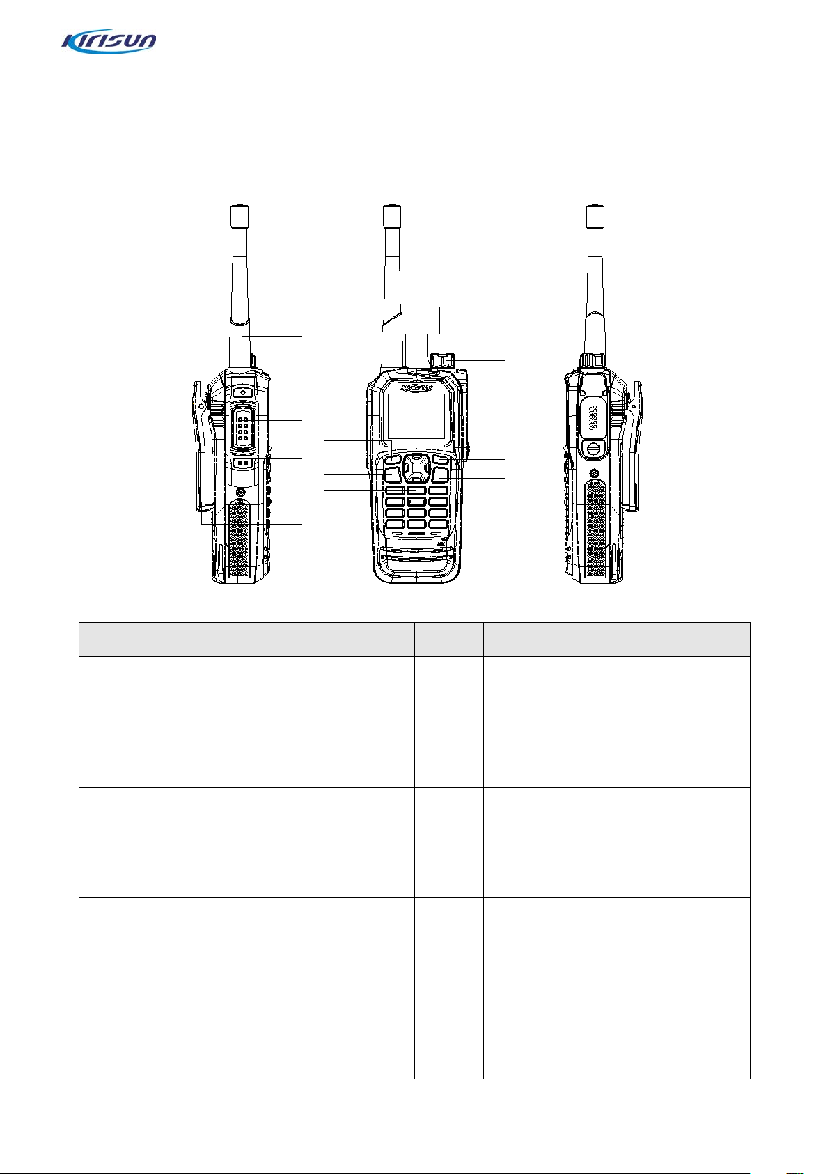
2. External View and Functional Keys
accessories.
D
M
N
O
P
G
H
J
K
I
L
R
Q
E F
A
B
C
2.1. External View and Functional Ke ys
DP770 Service Manual
No. Part Name No Part Name
Volume/Channel Knob
Rotate the knob to adjust the
A Antenna B
LCD Display
C
160*128, 65K colors, 1.8 TFT
LCD.
D
volume.Short press the key, the
feature of the knob switches from
adjusting the volume to changing
the channel.
Universal Connector for
Accessories
Connect USB program ming cable,
earphone or some other
E
G
I Side Key 2 (SK2) J Left Key
Top Key (TK)
Programmable, default: short
press to enable emergenc y alarm,
long press to exit emergency
alarm.
Side Key 1 (SK1)
Programmable, default: none.
F LED Indicator
H PTT Key
Page 4 of 102
Page 6

Programmable, default: none. Press the key to select the ite ms
Dial Key
K
M
O Numeric keypad P MIC
Q Speaker
Press the key to send data or t ext
messages.
Right Key
Press the key to select the ite ms
shown at the bottom right of the
screen.
L 4-way Navigation Key
N
2.2. LED Indicator
DP770 Service Manual
shown at the bottom left of the
screen.
ON/OFF/Hookoff Key
Return to the standby screen.
Long press the key to turn on/off
the radio.
• Red LED glows: Radio is transmitting.
• Green LED glows: Radio is receiving (voice, short m essage, or data) or there is an activity on t
c
hannel.
• Orange LED glows: This means the call hang time period. That is, you can press PTT to talk while t
or
ange LED glows
• Orange LED flashes: Radio is in e m er gency status; or there is a missed call / incoming call aler t ; or t
radio is scanning.
• Red LED flashes: Radio is r ec eiv ing emergency alarm or "power on check" failed.
he
he
he
Page 5 of 102
Page 7
3. Circuit Description
Pre-Driver2 Drive-stage
Final-stage Tx/Rx Switch Low-pass Filter
Microstrip
Matcher
APC
To RX
Gate voltage control
Subtracter
Sampling
resistor
BATT+
I/V
convertor
Attenuator
To GPS
TEMP
Sensor
Close To Final PA
Temp Det Level
Antenna
FGU
Pre-Driver1
3.1. RF Section
Figure 3-1 RF Schematic Diagram
DP770 Service Manual
3.1.1. Transmitter Circuit
Figure 3-2 Transmitter Circ uit Diagram
Page 6 of 102
Page 8

DP770 Service Manual
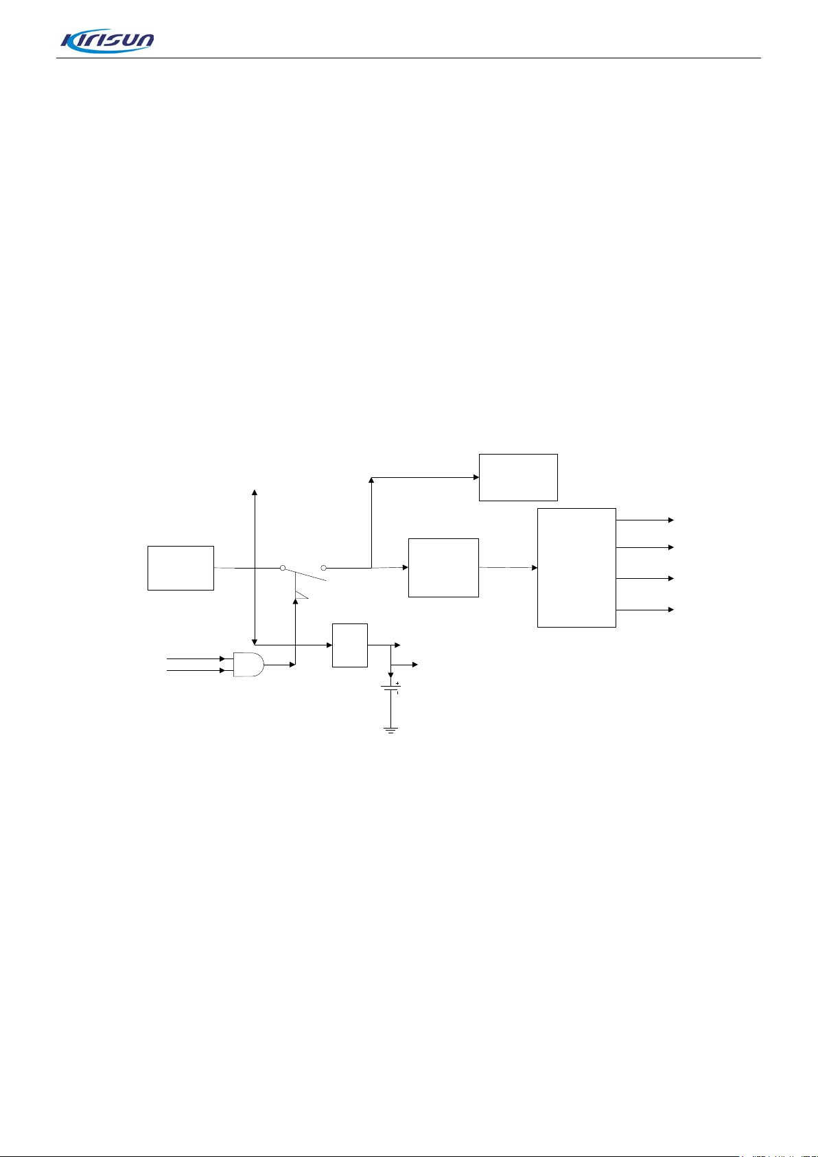
The transmitter circuit includes three parts:
• Tran smitter Power Amplifier
T
he carrier signal generat ed by the TX VCO is mod ulate d and a mpl ified, and f eeds to t he tr ansm itter circuit
via the following steps.
Step1: The signal passes a Π-type attenuator, realizing segregative isolation between RF power amplifier
circuit and TX VCO.
Step2: The signal are pre-amplified by a pre-driver amplifier (UHF: Q301, VHF: Q72), providing further
segregative isolation bet ween itself and the next level amplifier.
Step3: The signal goes to the next pre-am plifier and drive amplifier (RD01) to obtain further amplification,
guarantying to provide enough driver power signal to the final-stage amplifier (RD07) and obtain the final
power amplification..
Step4: After amplified by multiple amplifiers, the transmitter signal is processed by a microstrip line to
complete output impeda nce match ing at the output of f inal-sta ge amplifier, to reduce the output loss caus ed
by impedance mismatch.
Step 5: The transm itt er signal goes through the RX/TX switch and enters to the low-pass filter.
• Low-pass Filter Circuit of suppressing t he harmonics
The low-pass filter is high-grade low-pass filter composed of lumped-parameter inductors and capacitors.
By this filter, the spurious signal within the stop band can be attenuated as much as possible while the
in-band ripple is within the required range.
• Auto Power C ont rol Circuit (APC includes temperature detection circuit
I
n the auto power control and temperature detection circuit, the drain current from the driver amplifier and
)
final-stage amplifier is converted to voltage via the sampling resistor and subtraction circuit which is
composed of the first operat ional amplifier.
This voltage is compare d w ith the APC control voltage of output by DA C at the seco nd o perati ona l ampl ifier.
Then the error voltage controls TX power by controlling the bias voltage at the gate of amplifier (including
the driver amplifier and the final-stage amplifier. The temperature sensor IC detects the surface
temperature of the final-stage amplifier, and converts it to DC voltage. Then the DC voltage is compared
with the voltage correspo nding to t he protectio n temper ature (generally 80% of the extreme temperature ) of
the amplifier. If the temperature is too high, the b ias v oltage o f the a mpl ifier w ill be redu ced unt il the sur fa c e
temperature falls below the prot ec t io n temperature.
Page 7 of 102
Page 9
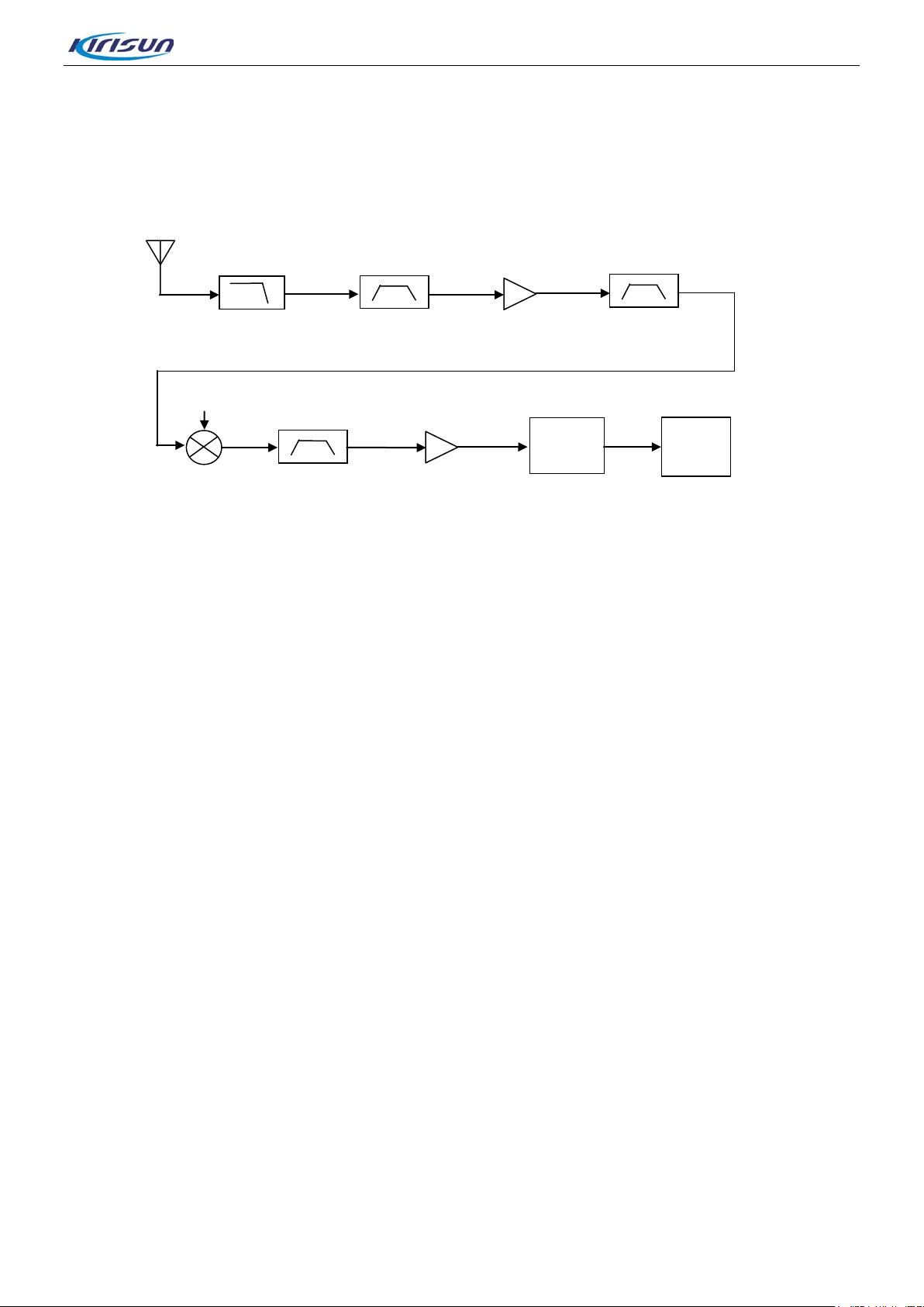
3.1.2. Receiver Circuit
AD986
Antenna
OMAP13
-120dBm
-106dBm
-121dBm
Clip at -24dBm
Figure 3-3 Receiver Circuit Diagram
DP770 Service Manual
Point A
Low-pass filter
Insertion los s = -1dB
-121dBm
-124dBm
Band-pass filter
Insertion los s = -3dB
Low noise amplifier
Gain = 18dB
Band- pass filte r
Insertion los s = -3dB
-109dBm
Lo: 0dBm
-115dBm
Mixer
Insertion los s = -6dB
he receiver circuit mainly com prises RF band-pass filter, low-noise amplifier, mixer, IF filter, IF amplifier
T
Crystal filter
sertion lo ss = -6dB
In
IF ampli fier
Gain = 25dB
Po-1dB = -24dBm
-96dBm
Point B
and IF processor.
• Receiver Front-end
The HF signal from the lo w-pass filter passes through the electrica lly t unab le band-pass filter controlled via
APC/TV1 level, to remove out-of–band interference signal and to send wanted band-pass signal to the
low-noise amplifier (UHF:Q205,VHF:Q62). The amplified signal goes to a band-pass fi lter controlled via
TFV level to remove out-of-band inter ference si gnal generat ed during a mplificat ion, and to send wante d HF
signal to the mixer (UHF:Z201,VHF:Z10).
Meanwhile, the first local oscillator signal generated by VCO passes through the low-pass filter and also
goes to the mixer (UHF: Z201, VHF: Z10). In the mixer, the wanted signal and the first local oscillator are
mixed to generate the first IF signal (UHF: 73.35MHz, VHF: 51.65MHz). The signal passes a frequency
selective network composed of LC, to suppress carrier other than the first IF signal , and to increase the
isolation between the mixer and the IF filter. After that, the first IF signal i s processed by the crystal filter
(UHF: Z202, VHF: Z11) and is sent to the two-stage IF amplifier circuit composed of 2SC5006 for
amplification. Then the amplified signal goes to the IF processor AD9864 (UHF: U201, VHF: U91) for
processing.
• eceiver Back-end
Figure 3-4 IF Processor Diagram
Page 8 of 102
Page 10
DP770 Service Manual
he first IF signal (73.35MHz) output by the IF amplifier goes into AD9864 (UHF: U201, VHF: U91) via Pin
T
47 and completes the second mixer, where the signal is converted to the second IF signal (2.25 MHz). The
second IF signal is converted to digital signal via ADC sampling, and output via the SSI interface. Finally,
the digital signal is sent to DSP (OMAP138) for demodulation.
AD9864 employs reference frequency of 12.8MHz. The second local oscillator is composed of an external
oscillator, a varactor and some other components, to provide the (UHF: 71.1MHZ, VHF: 49.4MHz)
71.1MHz LO signal. The 18MHz clock input frequency of AD9864 is generated by the LC resonance loo p.
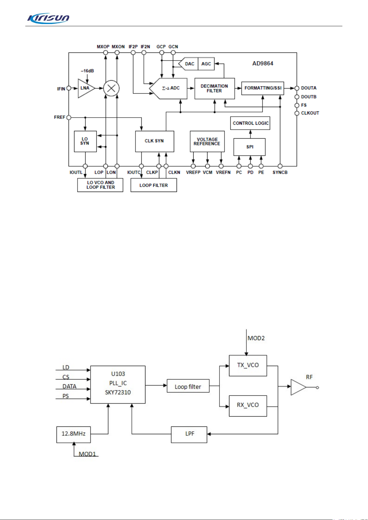
3.1.3. Frequency Generation Unit
Figure 3-5 Frequency Generation Circuit Diagram
Page 9 of 102
Page 11
DP770 Service Manual
The frequency generation circuit is composed of VCO and PLL. It is the core module of the whol e TX-RX
system. This circuit provides accurate carrier frequency during transmission; and provides stable local
oscillator signal during rec ept ion. It has a direct influence on the performance of the system.
• Workin g Pr inciple of PLL
The 12.8MHz frequency generated by the reference crystal oscillator goes to PLL for division, generating
the reference frequency (i.e step frequency f1). The frequency generated by VCO is filtered harmonic via
LPF and generates another frequency ( f2) through the freq uency div ider in PLL. Then freque ncies f1 an d f2
are compared in the phase detector (PD), to generate continuous pulse current. The pulse current goes to
the loop filter for RC integration and is then converted to CV voltage. Then the CV voltage is sent to the
varactor of VCO. It adjusts the output f requency of VCO directly unti l the CV voltage becomes constant.
Then the PLL is locked, and the stable frequency output by VCO goes to the TX-RX channel af ter passing
through two buffer a m pl ifiers.
• Workin g pr inciple of VCO
Voltage controlled oscillator applies oscillation mode of three-point capacitance, and gains different output
frequency through changing controlled voltage (C V) o f varactor. Rx VCO is composed of oscillating circuit
and Q24/Q29 and provides local oscillati on signal. Tx VCO is composed of oscillating circuit and Q27/Q28
and provides carrier of Tx signal.
Working principle employs colpitts oscillator circuit (the RX oscillator circuit is composed of D102, D103,
D106, D107 and L112 (VHF:D32, D33, D36, D34 and L23); the TX osci lla tor ci rcui t is com posed of D108,
D109, D110, D101and L117 (VHF:D38, D39, D40, D41 and L31). It obtains different output frequencies by
changing control voltage of varactor (i.e.CV voltage).RX VCO is composed of oscillator loop and Q104
(VHF:Q43), providing local oscillator signal. TX VCO is composed of oscillator loop and Q108 (VHF Q4 4)
and provides carrier of TX signa l.
• Two-point Modulation
To obtain higher modulatio n acc uracy and lower 4 F SK b it err or, it employs two-point modu lat ion tec hno logy
in the TX mode. MOD1 and MOD2 send the modulation signal to the modulation end of VCO and the
reference crystal oscillat or of PLL respectively to modulate TX VCO and the reference crystal oscillator.
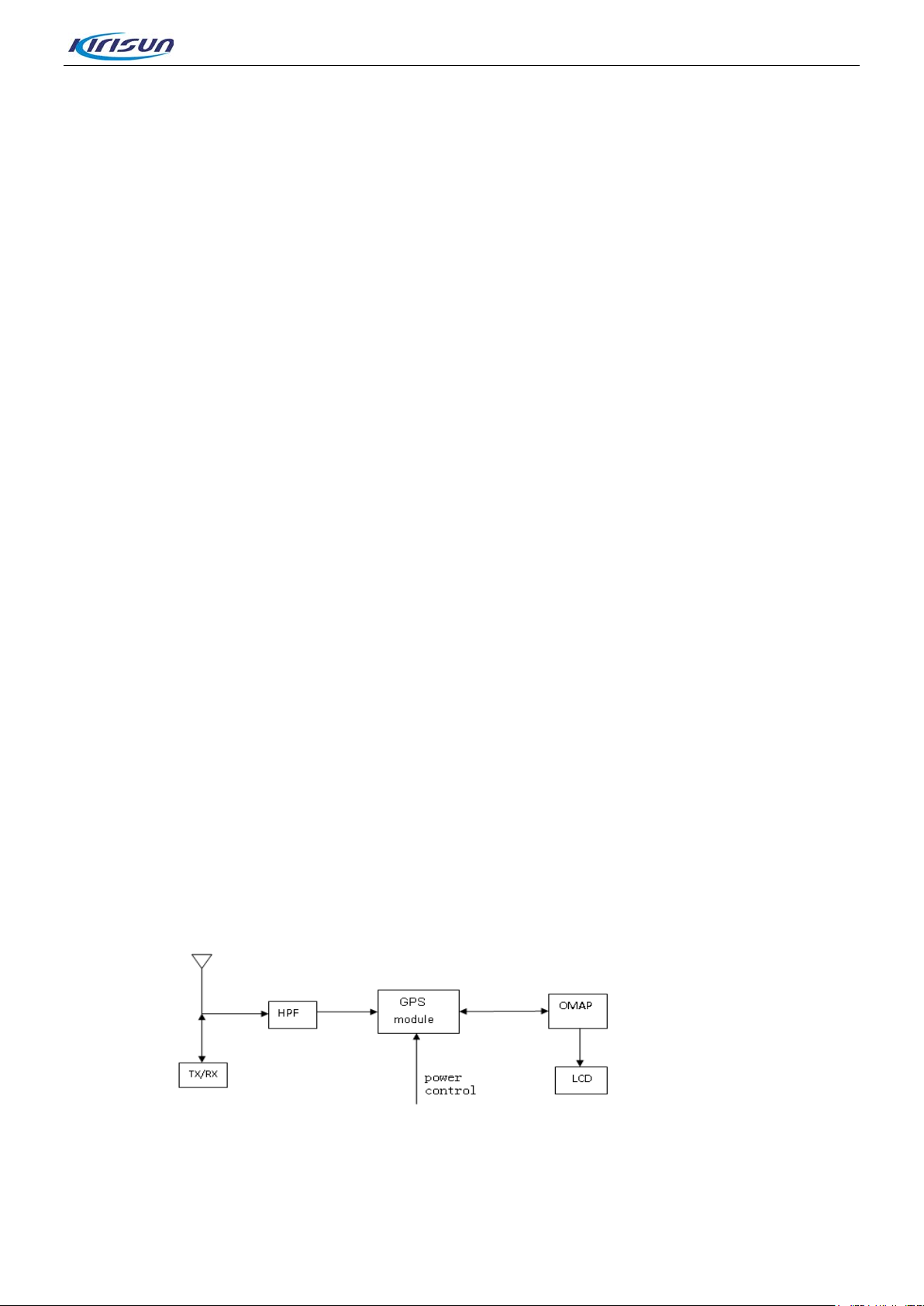
3.1.4. GPS Circuit
Figure 3-6 GPS Circuit Diagram
The GPS function is realized via REB-1315LPx (GPS module).The GPS module integrates a baseband
processor, a LAN and a SAW . The GPS function is realized via the foll ow ing steps:
Page 10 of 102
Page 12
DP770 Service Manual
PMU
VCC_3V3
VCC_1V8
VCC_1V2
LDO_3V3
V
C
C
_
5
V
0
Power switch
DC/DC
Battery
Audio PA
Soft_ctr
PWR_Key
RF_PWR
Logic OR
LDO
GPS_3v3
RTC_1v2
Step1: The 1575.42MHz GPS signal is received by the antenna, and then goes to HPF to remove the
in-band signals used for t r ansmission and reception.
Step2: The signal goes to GPS module for amplification and filtering after frequency selection via filter.
Then it will be sent to baseband section for cal culation.
Step3: The calculated GPS position information is sent to OMAP for processing via the UART interface.
Meanwhile, OMAP138 can send appropriate command information to the GPS module via the UART
interface.
Step4: Finally, the OMAP sends the proce ssed data information to the LCD.
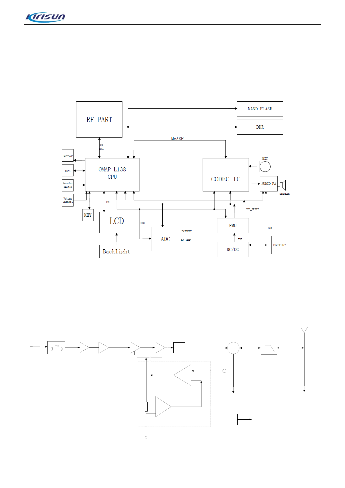
3.2. Baseband Section
3.2.1. Power Section
Figure 3-7 Power Section Diagram
The radio adopts 7.4V li-i
on battery as power supply. The baseband and RF circuit are supplied by
independent power structure. The baseband power is composed of two stage conversion circuit. The first
stage reduces the batter y voltage to 5V by DC/DC, and the second stage converts the 5V voltage to power
required voltage for the system by the power management.
Power On/Off: Power On/Off is implemented through a PMOS component. When the Power On/Off key i s
pressed, PWR_Key signal becomes high level, and PMOS component becomes conducted. The system
will begin initialization and set Soft_ctr to be high level. Thus, the radio is powered up. During the power off
process, when the system detects that the Power On/Off key is pressed, the system will begin executing
the shut down operations, and finally set Soft_ctr to be low level, which will shut down the PMOS
component, thus the radio being powered off.
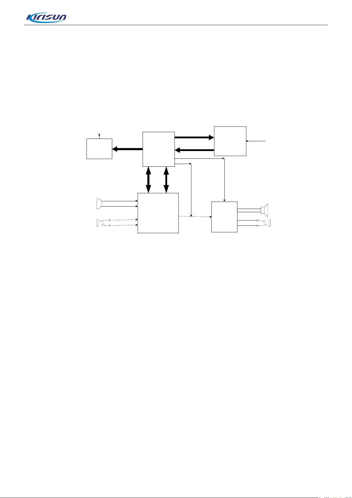
3.2.2. Audio Section
The audio module is mainly for audio input and outp ut. It uses TLV320AIC14 as audio codec to conv ert and
Page 11 of 102
Page 13
DP770 Service Manual
CODEC
Audio PA
OmapL138
AD9864
TLV5614
Baseband signal
Configure data
RX signal
RX
TX
IICIIS
INT_MIC
EXT_MIC
Voice signal
INT_SPK
Interface EXT-SPK
TONE
Mode
select
SPI
MIC
Input
PWM
Control
signal
process audio signal and digital signa l. The audio ampl ifier TDA854 7TS is used to amplify the analog audio
signal.
DSP processes digi tal signal (i.e audio signal encoding/decoding, digital I/Q signal decoding, digi tal audio
signal processing). The AD9864 converts and processes the RF IF, and sends un-demodulated serial
digital signal to the DSP fo r proces sing. The n DAC 5614 conv ert s the dig ital signa l output by DAS to analog
signal.
Figure 3-8 Audio Section Diagram
iagram of Signa l Flow
• D
The microphone convert s t he aud io sign al into e lectr ica l signa l, whic h is am plifi ed by PG A of the codec and
then sent to ADC of the codec for sampling. After digital audi o processing, the signal is output DSP for
processing. Then the s ign al is s ent t o DA C (TLV5614), which conver ts t he sig nal to modulat ion si gnal. After
modulated and amplified in the RF module, the signal is sent out from the antenna.
The RF signal receiv ed by the R F mo dule is conv ert ed to d igit al by ADC (AD9864), and is then sent t o D SP
for modulation and proces sing. Then the digital signal is sent to the digital audio process or of the codec for
digital audio processing, and is then converted into analog audio signal by DAC of the codec. Finally the
signal is amplified by the exter nal audio amplifier (TDA8547TS) to drive the speaker.
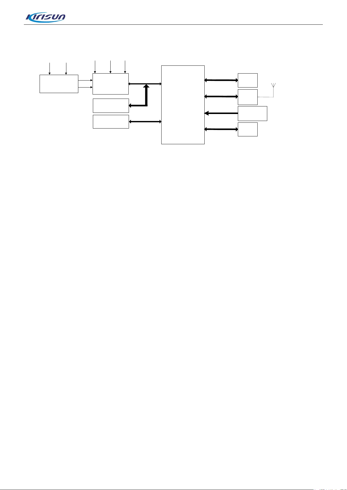
• System Peripheral Function Unit
The system peripheral consists of analog/digital converter module, vocoder encryption modul e, TF card
interface module, display module, key detection module and acceleration sensor module. These modules
are used to achieve human-radio interaction, state detection, communication encryption and feature
extension. The analog/digital converter is used for voice signal strength detection, power suppl y detection,
temperature detection, so as to realiz e VOX, low bat tery w arning and tem perature c ontrol. The ac celerati on
sensor is used to detect tilted state, realizing mandown function. The TF card module interface is used for
communication encrypt ion, to provide communicate security.
Page 12 of 102
Page 14
DP770 Service Manual
ADC
Voice level detect
Codec
Accelerometer
TF card
IIC0
INT_MIC
EXT_MIC
CVDECT
Voltage
Temperature
detect
IIC1
GPS
UART0
OmapL138
Key scan module
LCD
LCD
controler
Figure 3-9 The Composing of System Basic Peripheral
4. Function Instruction and Parameters Setting
4.1. General Functions
• Support P-Call, G-Call, A-Call in digit a l mod e.
• Support P-Call, G-Call, A-Call in analog mode.
• Support Transmit Interrupt function in digital mode.
• Support Encryption of both voice and data.
• Support Short message, st at us me ssage and GPS data information.
• Support Stun, Un-kill, Re mote Monitor, Call Alert digital signaling.
• Support Self-defined Ki ll digital signaling.
• Support CTCSS/CDCS S i n analog mode.
• Support MDC1200, 2 Tone, DTMF, 5Tone signaling system in analog mode.
• Support Emergency funct i on.
• Support scan function of digital channel, analog channel and mixed digital and anal og channel.
• Support the maximum of 1024 c hannels capacity.
• Support the maximum of 248 Z ones and the maximum of 128 channels in every zone.
• Support the maximum of 512 co ntacts.
• Support graphic menu operation interface.
• Support LED, choices of alert t ones and vibration indication.
• 12.5 kHz, 20 kHz or 25 kHz channel spaces can be chosen by PC software.
• Real-time display of signal strength.
• Support battery display and low bat t er y alarm alert functions.
Page 13 of 102
Page 15
DP770 Service Manual
4.2. Parameters Setting
Radios have default parameters. While users can set parameters of frequency, channels, function of
scanning or encryption, etc according your own requirements.
• Parameters setting st eps as follow:
Step 1. Install the right version of Kirisun CPSp.
Step 2. Connect radio with compu t er by Kirisun programming cable.
Step 3. Make sure radio’s power is on.
Step 4. Execute CPSp and start oper at ion.
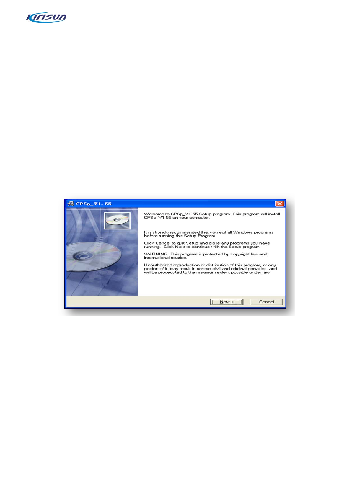
• CPSp installation st eps as follow:
Step 1. Double click the installation file; pop-up interface as Figure 4-1.
Figure 4-1
S
tep 2. Click “Next” and enter into t he nex t inter f ac e t o choose the installation route.
Step 3. In the interface shown in Figure 4-2, users can click “Browse” t o choose t h e ins tallat ion r oute, or
use the default route, and click ”Next” t o ent er t he next interface to choose language.
Figure 4-2
Page 14 of 102
Page 16
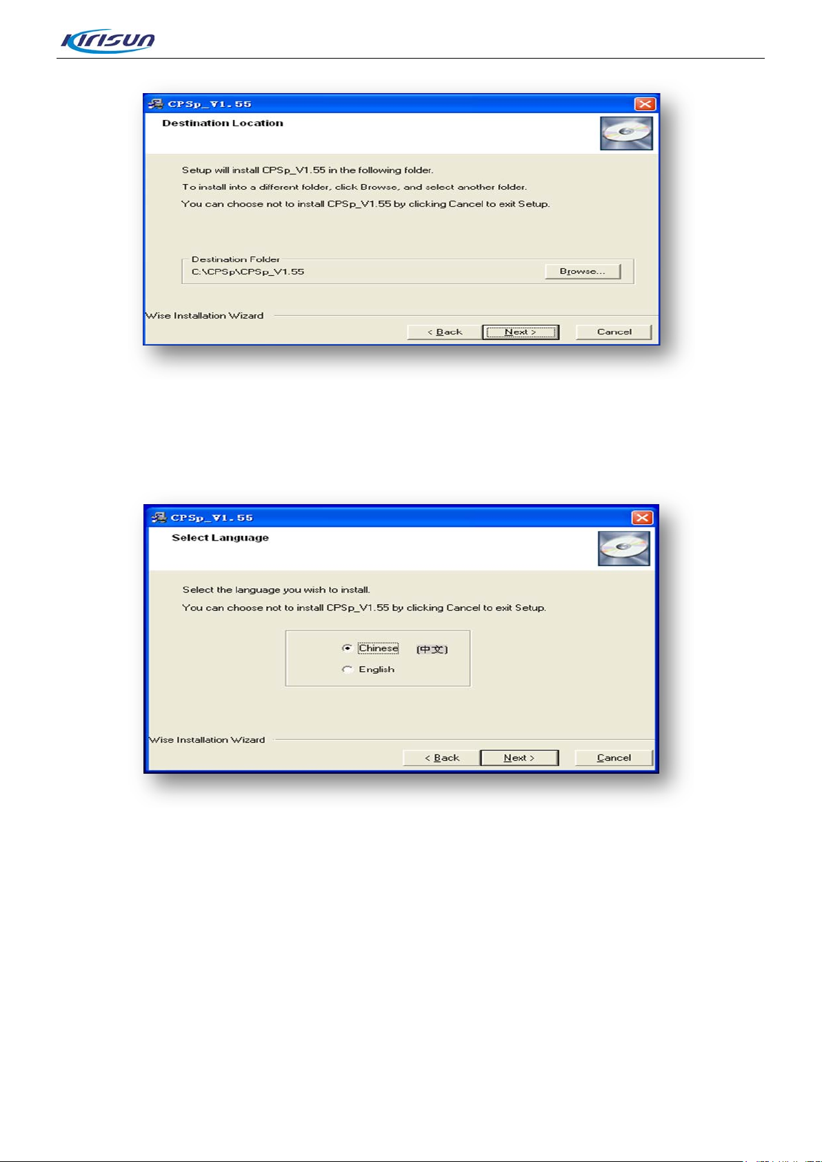
Step 4. Click “Next” to enter into installation information confirmation interface.
DP770 Service Manual
Figure 4-3
S
tep 5. Click “Next” to enter into the finished interface.
Figure 4-4
Page 15 of 102
Page 17
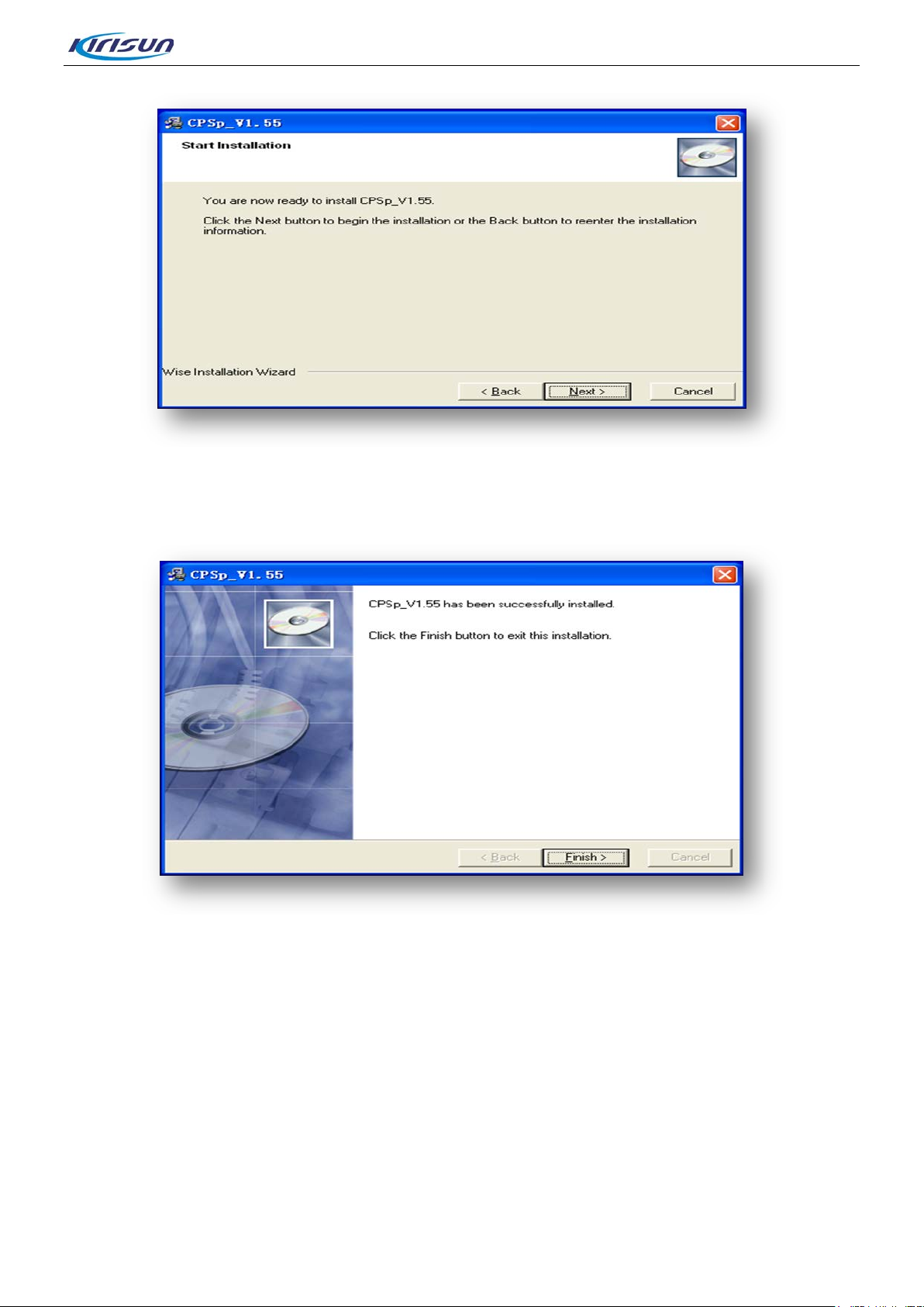
S
tep 6. Click “Finish” to finish installa tion.
DP770 Service Manual
Figure 4-5
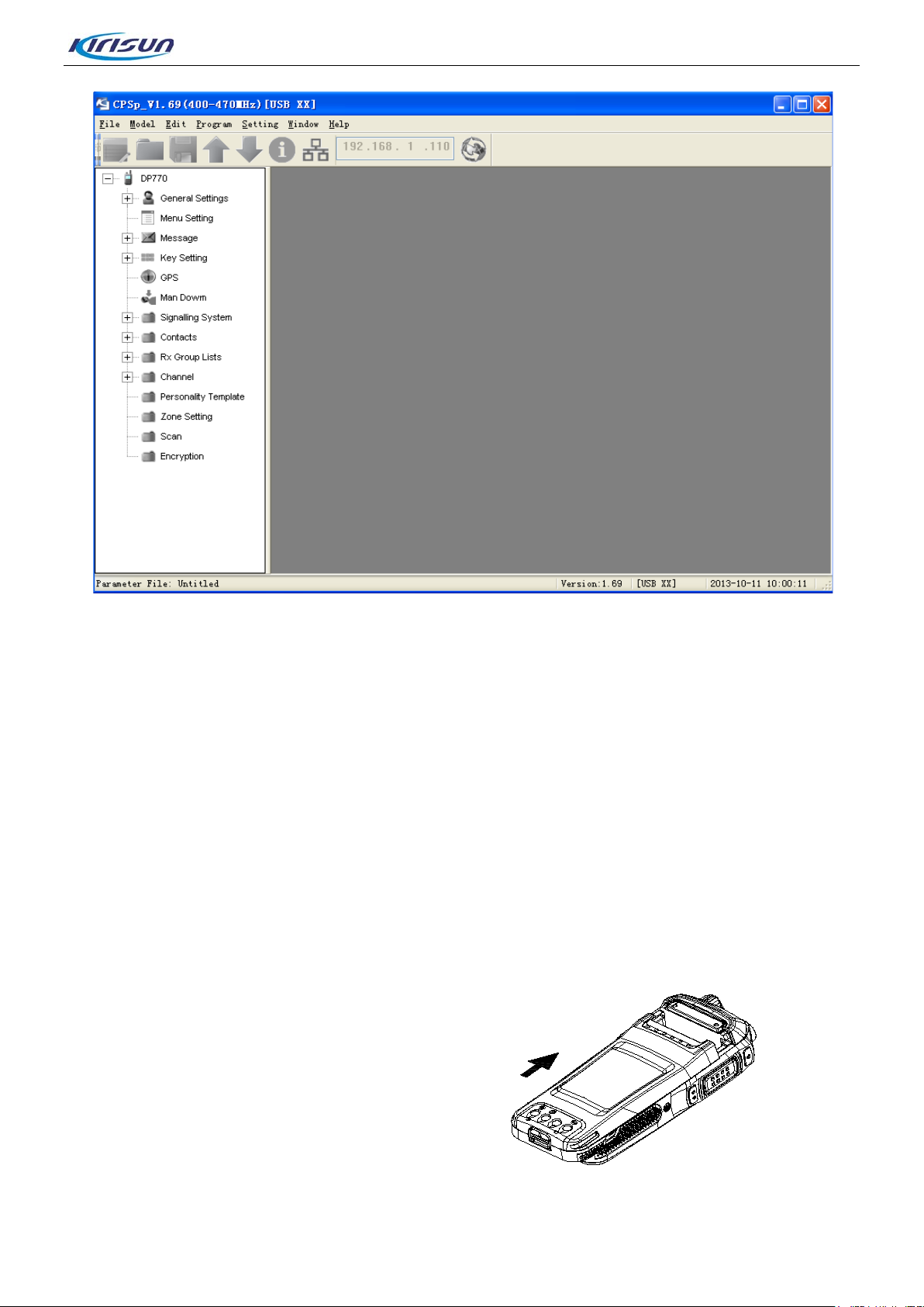
tep 7. After successful install at io n, double click the software, as shown in Figure 4-6
S
Figure 4-6
Page 16 of 102
Page 18
DP770 Service Manual
sers can read the radio’s date, or revise the data and then write into the radi o.
U
Please refer to the help file in t he C PSp for the detailed operation instruction about K ir is un CPSp.
Notes:
Errors of parameter configuration may make certain functions cannot be used properly, in general, which
can be solved by writing the correct par ameters configuration.
Before parameter configuration modification, we strongly recommend backup the current parameters,
make sure that the radio can rest or e after an error occurs.
5. Assembly and Disassembly
5.1. Attaching and Detaching the Battery
Attaching the battery as shown in figure 5-1.
Put the battery into radio’s aluminum alloy bracket slot.
Push up until a click is heard.
F
igure 5-1
Page 17 of 102
Page 19
Detaching the battery as shown in Figure 5-2
Push up the battery buckl e at the end of the battery.
Pull down to detach the bat t er y.
Figure 5-2
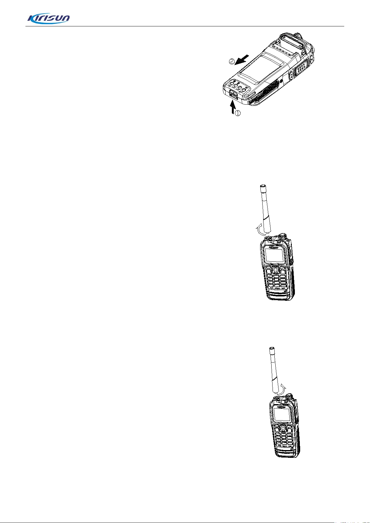
5.2. Attaching and Detaching the Antenna
As shown in Figure 5-3, put t he antenna into radio’ s t hread hole,
and rotate clockwise to fasten it.
DP770 Service Manual
As shown in Figure 5-4, rotate counter-cloc kwise to detach.
igure 5-3
F
igure 5-4
F
Page 18 of 102
Page 20
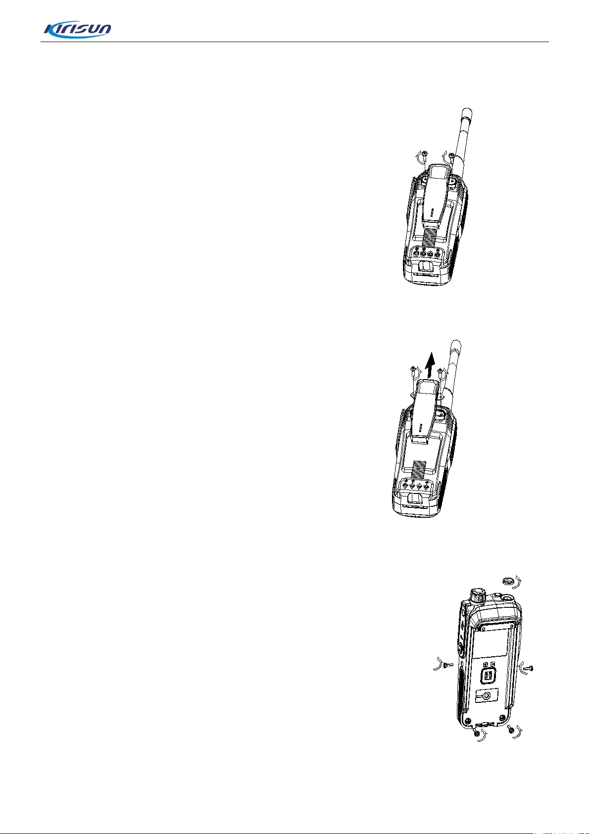
5.3. Attaching and Detaching the Belt Clip
As shown in Figure 5-5, align the screw holes on the belt clip, which is
located on the back of the r adio, and fasten them with the screwdriver.
DP770 Service Manual
Fi
gure 5-5
As shown in Figure 5-6, unfa s t en t he scr ews to detach the belt clip.
5.4. Detaching the Chassis
Step 1. Detaching the belt clip (Figure5.6);
Figure 5-6
Step 2. Removing the antenna (Figure 5.4);
Step 3. Removing the battery (Figure 5.2);
Step 4. Removing the two screws on the bottom of the chassis. Remove the
two screws on the side of shell, and remove the nut from antenna
connector.
Figure 5-7
Page 19 of 102
Page 21
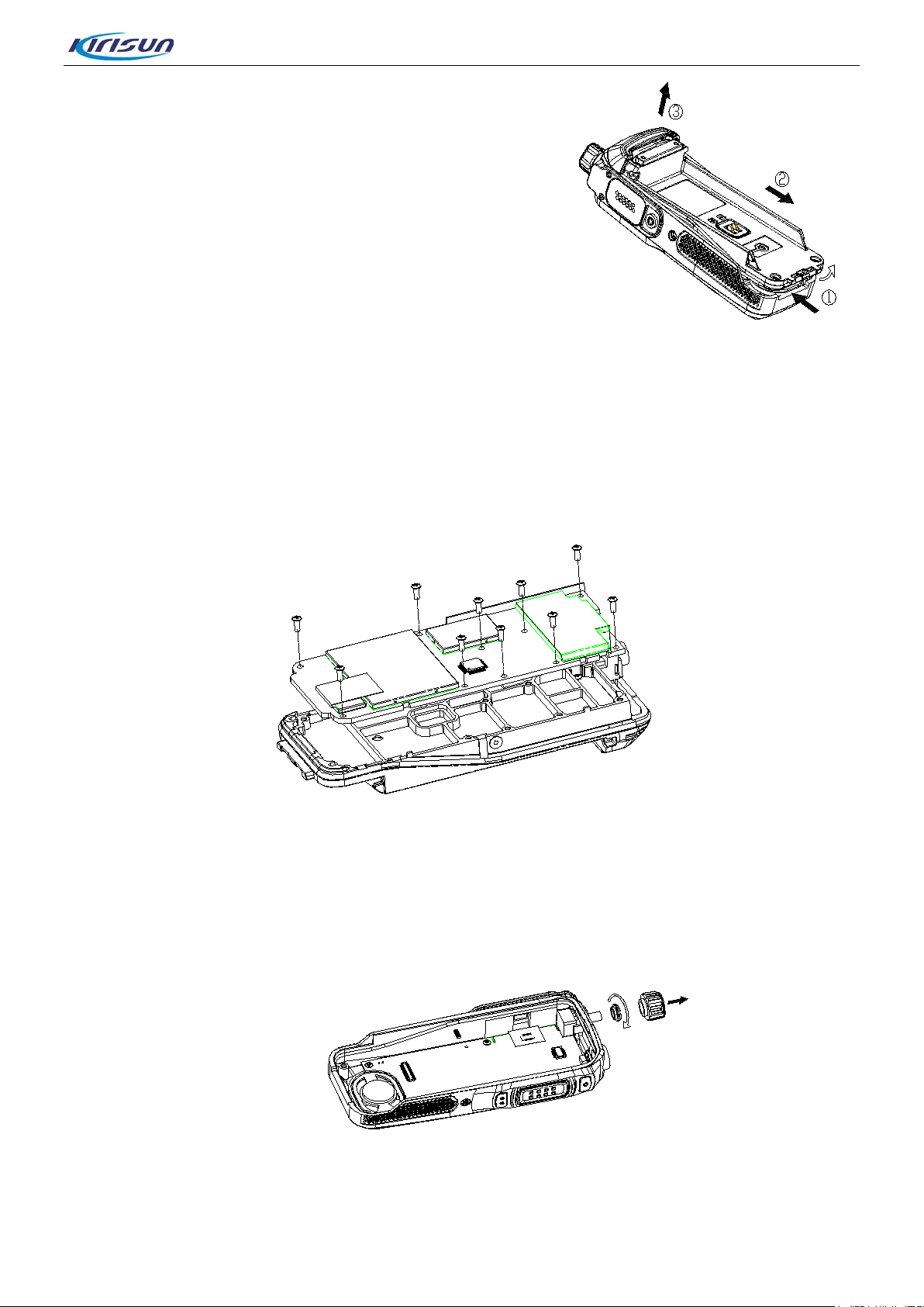
DP770 Service Manual
Step 5. Refer to Figure 5-8. Insert the flat-bladed screwdriver
into the slot of Al alloy bracket; lift it s o as t o separ ate the Zinc
alloy bracket from the chassis, and then push the Al alloy
bracket away from the chassis, and take the soft flat cable
away from the socket. Separate the speaker connecting cable
by the soldering iron to.
Fi
gure 5-8
5.5. Removing the PCB board from the Chassis
Step 1. Remove the ten screws on the PCB board.
Step 2. Cut off the antenna connecting point by the soldering iron and then separate the PCB board
from the chassis.
Figure 5-9
5.6. Detaching the Keypad Board from the Case
Step 1. Insert the flat-bladed screwdriver into the slot between the volume knob and case, lift the
volume knob and take off it. Remove the volume knob nut by special tool in the clockwise direction.
Separate the volume soft f lat c able from the socket.
Figure 5-10
Step 2. Separate the speaker and M IC cable by soldering iron.
Page 20 of 102
Page 22

DP770 Service Manual
Step 3. Remove the four screws from keypad board and take off keypad PCB from case. (See Figure
5-11)
Figure 5-11
ep 4. After the detaching above, you can make the appropriate repairs and debug against fault
St
conditions.
Page 21 of 102
Page 23
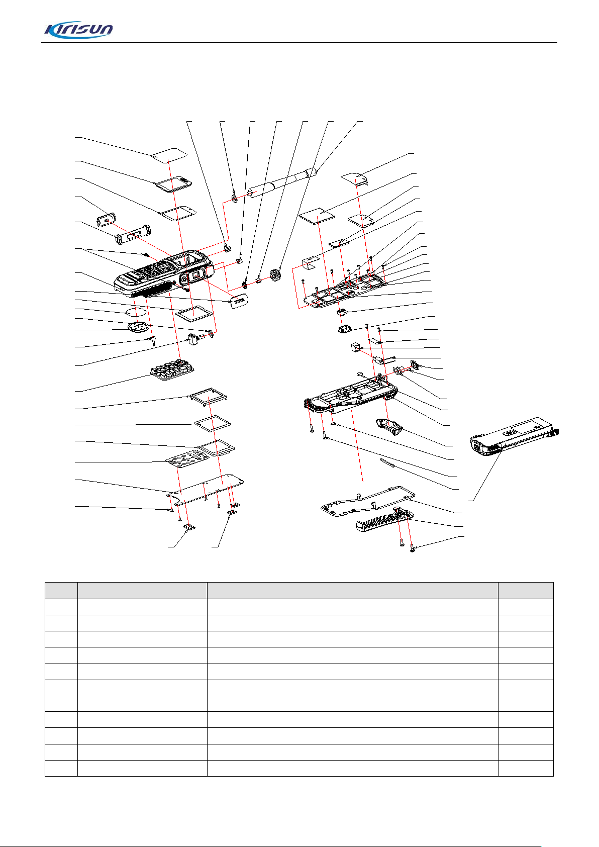
5.7. Exploded View
NO.
Part Number
Name, Specification
Quantity
1
7WFP-4002-01A
DP770lens protective fi l m PE T; transparent
1 2 7MHP-4002-02A-WC
DP770 LCD lens PC+PMM A, transparent
1 3 7GCJ-S4002-J
DP770 lens double sides adhesiv e t apeNITTO 57120B
1 4 7MHP-4002-04A-W9
DP770 PTT cover PC+ABS/TPU;black/PT2757C
1 5 7MHR-4002-10A-W6
DP770 Side silicone buttons silica gel; blue,PT654C
1
1
2.0X7.0 iron hardened tooth machine screw; Zinc
plating-black
7
7MHP-4002-01A-W0
DP770 front cover shell P C+ABS, texture, black
1 8 6SS1-4002-HL3C
Attachment plate strips ne s t ing
1 9 7MHM-4002-01A-W9
DP770 LCD Sponge bac k r ubber ; bla ck
1
57585960616263
53
54
55
56
52
46
45
47
48 49
50 51
44
42
41
18
40
43
38
37
36
35
18
39
32
33
34
29 30
31
27
26
25
24
28
22 23
21
20
19
18
17
16
15
13
14
12
11
9
8
7
10
30 6
5
3
2
1
4
DP770 Service Manual
Spare Parts List(Structure)
6
10 7GCB-S4002-01A DP770 T rumpet anti-dust mes h nylon; black 1
7SAF-020070M-SZYB-Z
2
Page 22 of 102
Page 24

DP770 Service Manual
11
7MHR-4002-16A-W9
DP770 Knob waterproof p ad silica gel; black
1
13
4SM7-4002-A40
Waterproof microphone with cover Φ7.0mm, height 2.8mm,
1
14
4SM7-4002-A40
Encoder switch RE11(Linjiwei)
1
PT432C/ character
DP770 display shielding cover 44.3*34.1*2.0MM,
21
7SMF-020040M-SZYB-N
M2*4 iron hardened tooth ma chine cross screw, Nylok
7
sided adhesive
1
M2.6*6 cross, machine ferrous hardened, Black zinc
machine teeth
25
6SS3-BJ4026-A
KBJ-15 Belt Clip PC+ABS
1
26
7MHR-4002-11A-W9
DP770 main waterproof ci r cle o f si li ca gel; black
1
1
2.0X11.0 tooth machine cross screws 5.3 harden iron; zi nc
plating-black
mesh
32
7MHP-4002-05A-W9
DP770 main unit top cover PC+ABS; texture; black
1
33
7MHL-4002-01-W
DP770 aluminum chasis ADC12; burnished
1
34
7MHR-7042-06B-W0
thermally conductive pad, blac k,3*6*9mm
1
DP770 Motor pressure pieces of stainless steel; natural
45
7MHC-4002-04A-W
DP770shielding cover ho lder 22.8*15.6mm; cupronickel
1
46
6PM7-4002-HMH
DP770-02 main board PC B ten -layer boar d
1
12 4SS7-3525-016-100A
15 7MHR-4002-09A-W9
DP770 speaker(waterproof)Φ=35mm,H=25mm,16Ω,
1W
DP770 The silicone number buttons;
with photopermeability
1
1
16 7MHS-4002-01A-W DP770 LCD Cupronickel stents; Xianfeng Hardware 1
17 7MHC-4002-11A-W
cupronickel
1
18 4PC7-4002H-A LCD display ZYW-T18CP-20PJ-B 1
19 7MHS-4002-03A-W
Numeric key METAL DO ME dia meter 4.0;SUS301
1
20 6PM7-4002-HKG DP770KEY-LCD PCB Four-layer board 1
22 7GCM-180090015-J
23 7GCM-100090015-J
24
7SMF-026060M-SZHT-B
DP770 main board double-s ided adhe sive f oam bl ack f oam
18*9*1.5
LCD Socket black foam doublefoam10*9*1.5
1
2
2
27 6SS3-DC7198-A KB-77B battery 1
28 7MHM-4002-02-W Aluminum chasis Poron , liner, Poron 36.5*2.5*1.0 1
29
7SAF-020110M-SZYB-Z
2
30 7MHR-4002-19A-W9 DP770 Screw waterproof r ubber r in g; black;polished 4
31 7GCB-070045005-J
Φ7 Microphone protection water perforated film with plastic
2
35 3CR7-SMA-50JF-4 Antenna connector SMA-J, Flange installation 1
36 7MHR-4002-15A-W9 DP770 antenna connector Waterproof pad silicone;blac k 1
37 4MV3-KFF081522 φ8Dc motor vibration KFF081522 1
38 7MHR-4002-17A-W9 DP770 Motor silicone pad sil ica gel; black 1
39 7MHS-4002-02A-W
color; Junyu, lead free
1
40 7MHR-4002-18A-W9 DP770 Discharge seatin g silicone; black 1
41 7MHP-4002-01A-W TD7700 battery connector BC-2P-41PH-6.8H 1
42 7MHC-4002-02A-W
DP770 shielding cover hol der一 43.4*32.3mm; cupronickel
1
43 7MBM-S4002-A EMI Gasket 12*7*7 With double-sided adhesive 3
44 7MHC-4002-16A-W1 GPS shielding cover base , c upronickel; Junyu; Lead free 1
Page 23 of 102
Page 25
DP770 Service Manual
M2*5 plum blossom iron hardened tooth machine screw,
49
7MHS-4002-04A-W
DP770 PTT key METAL DOME4.0; SUS301
1
50
7MHS-4002-05A-W
DP770
,0.6mm
1
51
7MDZ-1737-04A-J5
KB-58L sticker 1
,8*35*0.2
1
52
6SS1-4002-HL1G
Main flat cable
1
46.85x32.25x0.15mm
63
7MHR-4002-12A-W3
DP770 emergency key silica gel key;orange,PT021C
1
47
7SMF-020050M-MHHTN1
nickel plating
10
48 6PD7-4002-HPC DP770PTT board PCB double side board 1
Platooninsert tabletting stainless steel
Barley paper
53 7MHC-4002-05A-W DP770 shielding cover 23.3* 16. 1mm; cupronickel 1
54 7MHC-4002-17A-W1 GPS shielding cover cupronickel; Junyu; lead free 1
55 7MHC-4002-03A-W DP770 shielding cover 43.9* 32. 8mm; cupronickel 1
56 7MHJ-4002-01A-W
GPS
hielding cover conductive fabric
s
1
57 8ATX-400470-WC DP770 dual mode ant enna 400-470MHZGPS antenna 1
58 7MHP-4002-03A-W9 DP770 knob PC+ABS/TPU, grey 1
59 7MHS-1767-02B-W PT6800Knob circlip stainless steelSUS30 4-1/2H, hardened 1
60 7NRC-077107040-Z R 7200 Coding switch nut br ass , zinc plating-black 1
61 7MHR-4002-13A-WC DP770 Guide pillar silicon e; transparent 1
62 7NRC-090110025-W1 Ant enna connector copper nut 1
Page 24 of 102
Page 26
6. Tune Mode
Low
Frequency
Mid-frequen
cy
High
frequency
Low
Frequency
Mid-frequen
cy
High
frequency
It may need to check and adjust t he par ameters after parts replacement in maintenance.
6.1. Required parts in adjustment
(1)Antenna adapter
(2)Universal interface
6.2. Adjusting and checking method
6.2.1. Frequency descri ptio n
Model 400~470MHz
DP770 Service Manual
Channel
TX frequency(MHz) 400.00 435.00 470 400 410 420 430 440 450 460 470
RX frequency(MHz) 400.05 435.05 469.95 400.05 410.05 420.05 430.05 440.05 450.05 460.05 469.95
Model 136~174MHz
Channel
TX frequency(MHz) 136.00 158.00 174.00 136.00 140.00 146.00 152.00 158.00 164.00 170.00 173.975
RX frequency(MHz) 136.05 158.05 174.00 135.05 140.05 146.05 152.05 158.05 164.05 170.05 174.00
F1 F2 F3 F4 F5 F6 F7 F8
F1 F2 F3 F4 F5 F6 F7 F8
Page 25 of 102
Page 27
6.2.2. Adjustment Equipments
Test
equipment
1)Enter tune mode;
5) Click “Save” to save it.
1)Enter tune mode;
2)Double click TX high power, and enter
frequency F1 to F8 to adjust high power
3)Adjust the value in tune mode to make
frequency F1 to F8 to adjust low power
3)Adjust the value in tune mode to make
(1)Comprehensive t est inst r ument(HP8921 or similar equipment)
(2)Computer and CPSp software
(3)AEROFLEX 3920
(4)spectrum analyzer
6.2.3. Adjustment instruction of TX
Test Tool and Method Remark
Item Configuration
Test Point Tool Method
DP770 Service Manual
Frequency
Stability
Tx High
Power
Tx Low
Power
Set comprehensive instrument
to tx mode
Set comprehensive instrument
to tx mode
Set comprehensive instrument
to tx mode
HP8921A or
similar
instrument
HP8921A or
similar
instrument
Connect the
antenna port to
RF IN/OUT port of
instrument by
antenna
connector adapter
PC
2)Double click frequency stability
3)Adjust the value in tune mode to make
the tx frequency to be within+/-480Hz
4) Observe TX current
output at different frequency.
the tx high power to be within 4W+/-0.2W
4) Click “Save” to save it.
1)Enter tune mode;
2)Double click TX low power, and enter
output at different frequency.
the tx high power to be within 1W+/-0.2W
4) Observe TX current
5) Click “Save” to save it.
≤±500Hz
1) Power:3.7W-4.5W;
2) Current:<1.8A
1)
Power:0.7W-1.5W;
2) Current:<1A
Page 26 of 102
Page 28

DP770 Service Manual
1)Enter tune mode
Double click” Low frequency modulation
and enter to F1 to F8 to adjust
FM deviation on the instrument when AF
1)Enter tune mode
deviation” and enter to F1 to F8 to adjust
FM deviation on the instrument when AF
Click “Start”, the radio will enter vox
Maximum
Deviation
Low
frequency
modulation
deviation
High
Frqnecy
modulation
deviation
Set the test instrument to tx
mode.
Set HF(High filter) to 50Hz
and LF(low filter) to 15KHz
)
Set comprehensive
instrument to tx mode
Set comprehensive
instrument to tx mode
H
P8921A or
similar
instrument
HP8921A or
similar
instrument
HP8921A or
similar
instrument
Connect the
antenna port to
RF IN/OUT port
of instrument by
antenna
connector
adapter
Connect the
antenna port to
RF IN/OUT port
of instrument by
antenna
connector
adapter
Connect the
antenna port to
RF IN/OUT port
of instrument by
antenna
connector
adapter
PC
PC
PC
1) Enter tune mode;
2) Double click "Maximum Deviation".
3)Adjust the value in tune mode and view
the FM deviation on the test instrument
4) Make the FM deviation within 5.0±0.05kHz
5) Click confirm to save
2)
deviation”
different frequency.
)Adjust th e valu e in tun e mo de an d view the
3
Freq is 0.1kHz
4
)Make the FM deviation within
5.0±0.05kHz.
5)Click save to save the data.
2)Double click” high frequency modulation
different frequency.
)Adjust th e valu e in tun e mo de an d view the
3
Freq is 6.0kHz
4
)Make the FM deviation within
5.0±0.05kHz.
5)Click save to save the data.
4.95kHz-5.05kHz
4.95kHz-5.05kHz
4.95kHz-5.05kHz
Set comprehensive
VOX 1
instrument to tx mode 1)
AFGen1 Freq:1kHz;
2)AFGen1 Lvl:50mV
HP8921A or
similar
instrument
Connect mic
port of the radio
to audio out of
test instrument
PC
1)Enter tune mode
2)Double click”VOX1.
3)
adjustment automatically.
4
)Click “stop” when the value is stable.
5)Click save to save the data.
Test:
1)The vox will activate then
AFGen1 is set to50mV.
The vox will stop when
AFGen1 is below 15mV.
Page 27 of 102
Page 29
VOX 10
The low battery starts to
the voltage is above 7.2V.
1)Enter tune mode.
4) After adjustment, click save
Equipment
Connect the
by test cable
Low battery
warning
Set comprehensive
instrument to tx mode 1)
AFGen1 Freq:1kHz;
2)AFGen1 Lvl: 5mV
HP8921A or
similar
instrument
* multimeter
Connect mic
port of the radio
to audio out of
test instrument
Battery
connector
PC
*
1)Enter tune mode
2)Double click”VOX10”.
3) Click “Start”, the radio will enter vox
adjustment automatically.
4)Click “stop” when the value is stable.
5)Click save to save the data.
1)Enter t tune mode
2)Set the power supply voltage to 6.8V;
3)Click save when value is stable.
DP770 Service Manual
*
work when the voltage is
below 6.5V.
The radio will power off
when the voltage is below
5.8V.
The radio can work when
CV Curve PC
6.2.4. Receiver section adjustment instruction
Item Configuration
Receiver
sensitivity
1)Set comprehensive
instrument to RX mode
2)Set RF Gen Freq to F1、
F2、…、F8,Eg:Set RF Gen
Freq to 469.95MHz when
testing F8
3)Set AFGen1 Freq to 1kHz
Set AFGen1 to 3kHz
4)Set HF(High filter) to 300Hz
and LF(low filter) to 3KHz
2)Double click “TX CV Curve”
Click “Start”
3)
Test Tool and Method
Test
Test point Tool Method
antenna port to
HP8921A or
similar
instrument
RF IN/OUT port
of instrument by
antenna
connector
adapter, Connect
universal
connector
of
radio to audio in
PC
1) Enter tune mode
2) Double click “receiver sensitivity”. Enter F1
to F8 to adjust different frequency.
3)Set input signal strange to -119dBm, adjust
pc value to max the SINAD and the SINAD
is above 12dB .
4)Click save to save it.
of test instrument
Low point:>=0.5V
High point:<4.5V
Standard
Requirement
SINAD>=12dB
W:-119dBm;
N:-118dBm。
Page 28 of 102
Page 30

SQL1 Open
1)Set comprehensive
1.5kHz(N)
1)Set comprehensive
1.5kHz(N)
1)Set comprehensive
1.5kHz(N)
1)Set comprehensive
1.5kHz(N)
SQL1 Close
SQL9 Open
SQL9 Close
instrument to RX mode
2
)Set RF Gen Freq to test
frequency
3)Set Amplitude t
-123d
Bm1(25KHz)or -121dBm
o
(12.5KHz)
4)Set AFGen1 Freq to 1kHz
5)Set FM to 3kHz(25KHz)
instrument to RX mode
2
)Set RF Gen Freq to test
frequency
3)Set Amplitude t
-125d
Bm(25KHz)or -123dBm
o
(12.5KHz)
4)Set AFGen1 Freq to 1kHz
5)Set FM to 3kHz(25KHz)
instrument to RX mode
2
)Set RF Gen Freq to test
frequency
3)Set Amplitude to -116dBm
4)Set AFGen1 Freq to 1kHz
5) Set FM to 3kHz(25KHz)
instrument to RX mode
2
)Set RF Gen Freq to test
frequency
3)Set Amplitude to -119dBm
4)Set AFGen1 Freq to 1kHz
5)Set FM to 3kHz(25KHz)
or
HP8921A or
similar
or
instrument
or
or
Connect the
antenna port to
RF IN/OUT port
of instrument by
antenna
connector
adapter
PC
DP770 Service Manual
1. Enter tune mode
2. Double click”SQL1 Open”and enter to F
o F8 to adjust different frequency
t
1
3. Click “Start”.
4. Click “Stop” when the value is stable.
5. Click save
1.Enter tune mode
2.Double click”SQL1 Open”and enter to F1 t
8 to adjust different frequency
F
3. Click “Start”.
4. Click “Stop” when the value is stable.
5. Click save
1.Enter tune mode
2.Double click”SQL9 Open”and enter to F1 t
F
8 to adjust different frequency
. C
3
lick “Start”.
4.Click “Stop” when the value is stable.
5.Click save
1.Enter tune mode
2.Double click”SQL9 Close”and enter to F1 to
F8 to adjust different frequency
. C
3
lick “Start”.
4. Click “Stop” when the value is stable.
5.Click save
Open:-119dBm
Close -127dBm
o
o
Open:-115dBm
Close -120dBm
Page 29 of 102
Page 31

RSSI 1
Connect the
adapter
Install standard double
、
RSSI 4
1)Set comprehensive
instrument to RX mode
2) Set RF Gen freq to 400MHz
3)Set Amplitude to -110dBm
1)Set comprehensive
instrument to RX mode
2) Set RF Gen freq to 400MHz
3)Set Amplitude to -80dBm
HP8921A or
similar
instrument
HP8921A or
similar
instrument
Connect the
antenna port to
RF IN/OUT port
of instrument by
antenna
connector
adapter
antenna port to
RF IN/OUT port
of instrument by
antenna
connector
PC
PC
1.Enter tune mode
2.Double click ”RSSI1”
. C
3
lick “Start”.
4.Click “Stop” when the value is stable.
5.Click save
1.Enter tune mode
2.Double click ”RSSI4”
3. Click “Start”.
4.Click “Stop” when the value is stable.
5.Click save
DP770 Service Manual
The RSSI is
displayed one
bar when input
signal is
-107dBm The
RSSI is
displayed 4 bars
when input
signal is
-70dBm.
1.Enter tune mode
2.Double click ”CV Curve”
. C
3
CV Curve
Test the VCO voltage
PC
lick “Start”.
4.Click “Stop” when the value is stable.
5.Click save
6.2.5. GPS Performance Test Instruction
Item Test Environm e nt Test Equipment Test Method Standard Requireme nt
1、 TTFF(cold start)Time to first fix
GPS
Position
Time
1) Change the radio to
digital channel
2)
mode antenna
3) Put the radio in the
outside area without high
building surround it.
1) DP770
2) Timing tool
1) Remove the battery
2) Install the battery
3) Open GPS function in the menu and
enter “gps information menu”
4) Activate timing tool
5) Check the time when gps positions
successful.
<1minute
2
TTFF(hot start)Time to first fix
<10 seconds
3、
Horizontal Accurancy
<10 meters
Low point:>
=0.5V;
High point:<
4.5V。
Page 30 of 102
Page 32

7. Main Specifications
General Specifications
Frequency
UHF1: 400-470MHz, VHF: 136-174MHz
Channel Capacity
1024
Channel Spacing
12.5kHz/20kHz/25kHz
Dimension
138mm*62mm*38mm
Display
1.8 Inches 65535 Color Display
Battery Capacity
7.4V 2000mAH Li-ion
Digital: 15 Hours
Environmental Operating Conditions
Working Temperature
-30℃~+60℃
Storage Temperature
-40℃~+85℃
Waterproof/Dustproof
IP67
MILST
Humidity
Shock and Vibration
Receiver Part
Frequency St a bi lity
±1.5ppm
DP770 Service Manual
Weight
Working Time(5-5-90)
Electrostatic Defending
362g(with battery and antenna)
Analog: 13.5 Hours
IEC 61000-4-2(Level 4)
±8kV (Touch)
±15kV (Air)
MIL-STD-810 C/D/E/F/G
MIL-STD-810 C/D/E/F/G
MIL-STD-810 C/D/E/F/G
Analog Sensitivity
0.3uV(12dB SINAD)/0.22uV(12dB SINAD,Typical)
Page 31 of 102
Page 33

DP770 Service Manual
Intermodulation
Spurious Response Rejection
Conducted Spurious Emission
Block
Rated Audio Power
Hum and Noise
Audio Respons e
Transmitter
Frequency St a bi lity
Hum and Noise
FM Modulation
Modulation Limit
Audio Respons e
+1dB~-3dB
Digital Sensitivity
Adjacent Channel Selectivity
Rated Audio Distortion
RF Power output
0.3uV(5% BER)
ETSI: 65dB TIA603: 70dB
ETSI/TIA603: 60dB@12.5kHz,70dB@20/25kHz
ETSI/TIA603: 70dB
-57dBm
ETSI: 84dB TIA603: 80dB
0.5W
<3% (Typical)
-40dB@12.5kHz/-43dB@20kHz/-45dB@25kHz
+1dB ~ -3dB
±1.5ppm
Low: 1W, High: 4W(UHF)/5W(VHF)
Conducted/Radiated Em issi on
Adjacent Channel Po we r
4FSK Modulation
-40dB@12.5kHz/-43dB@20kHz/-45dB@25kHz
-36dBm@<1GHz,-30dBm@>1GHz
60dB@12.5kHz,70dB@20/25kHz
11K0F3E@12.5kHz,14K0F3E@20kHz,16K0F3E@25kHz
12.5kHz(data only): 7K60FXD
12.5kHz(data and voice ): 7K60FXE
±2.5kHz@12.5kHz, ±4kHz@20kHz, ±5kHz@25kHz
Page 32 of 102
Page 34

DP770 Service Manual
Vocoder
Digital Data Protocol
GPS
Horizontal Accuracy
<10meters
Installations
Main Specifications
Frequency: 10MHZ to 3G Hz
Output:-127dBm/0.1uv---47dBm/1mv
Frequency Deviation Meter
Input Impedance:10Mega Ohm Impedance
Oscillograph
Frequency Stability: ≤ 0.2ppm
Ammeter
5A
Audio Distorti on
TTFF(cold start) Time to first fix
TTFF(Hot start)Time to first fix
3% (Typical)
AMBE++
ETSI TS 102 361-1, -2, -3
<1min
<10s
8. Repairing and Testing Equipments
RF Standard Signal Gen erat or (SSG)
Modulation: Frequency modu lation and externa l mode m
Dynamometer Instruments
Digital RMS Multimeter
High Sensitive Frequency Counter
Input Impedance: 50Ω
Operating Frequency : 100MHZ-1000MHz
Range: 10W
Frequency: 100MHZ-1000MHz
Range: DC 10mv-10v
30MHz- 100MHz
Frequency: 100-1000MHz
Page 33 of 102
Page 35

DP770 Service Manual
Output: 0-1v
Input PWL: 50mv-10vms
Spectrum analyzer
Range:100-3GHz or higher
16Ω Dummy Load
Power Supply
Output Voltage 5v- 30v, current:5A
No.
Problem
Causes and Solutions
You cannot communicate with
During receiving, LED is green
Audio Frequenc y Voltmeter
Tone Generator
Distortion Meter
9. Basic Troubleshooting
A.The battery may be used up. Recharge it or change the battery to try again.
1 The radio cannot be powered on.
B.The power ON/OFF key may suffer from poor contact. Clear the metal dome with alcohol and try again.
C.The power binding post isn’t connected with battery. Re-install it and try again.
D.The power is connected inversely which leads to the pow er prote ctive t ube F901 op en. R eplace t he pr otectiv e tube F901 and try again .
Frequency: 50Hz-10KHz
Voltage: 1mv-10v
Frequency: 50Hz - 5K Hz or higher
Power: when 1KHz, ≤3%
16Ω, 3W
2
3 The radio cannot receive signals
4
other members
but no voice.
A.The frequency settings may be different from others. Set your TX/RX frequencies to be the same as others.
B.The CTCSS/CDCSS signaling may be different from others. Set your CTCSS/CDCSS signaling to be the same as others.
C.Your place may be too far away from the others, beyond the radio’s coverage area.
A.The antenna may get looser or may be improperly installed. Re-inst all the ant e nna.
B.The frequency settings may be different from others. Set your TX/RX frequencies to be the same as others.
C. Your place may be too far away from the others, beyond the radio’s coverage area.
A.Check whether the volume is smallest or not. If so, increase the volume.
B.Check whether the speaker is broken or not. If so, change the s peaker.
Page 34 of 102
Page 36

5 GPS cannot locate your position.
DP770 Service Manual
A. Check whether the antenna is GPS+UHF dual band or not. If not, use a GPS+UHF dual band antenna to replace the old one.
B. Check whether the GPS setting is correct or not. If not, set it correctly.
C. Maybe there is some other RF interference around the radio’s place. Go to an open sky place and try again.
6
CPS programming failed.
A.Connection between the radio and PC is not good enough. Check and try again.
B.Earphone interface board has poor contact with external programming cable. If so, change the Earphone interface board.
Page 35 of 102
Page 37

Appendix 1 Material List(Electrics Parts)400-470MHz
BD+GPS)
main board SMD
4
1DR1-1SR154-400
R SMD commutation diode
1
D903
12
1DV1-HVC376B
R SMD varactor
9
D101,D102,D105,D106,D202,D203,D204,D205,D206
B
,
NO. Part Number Name Quantity Position Mark
DP770 Service Manual
1 6SS2-4002B-HMD
2 6SS1-4002B-HMC
3 0SS1-4002B-HME
5 1DS1-DA2S10100L R SMD switch diode 9
6 1DS1-DAN222 R SMD switch diode 1 D904
7 1DS1-HSC277 R SMD switch diode 1 D112
8 1DS1-HVC131 R SMD switch diode 4
9 1DV1-1SV278 R SMD varactor 1 D109
10 1DV1-1SV305 R SMD varactor 1 D201
11 1DV1-HVC350B R SMD varactor 4 D103,D104,D107,D108
DP770 Main Board suite(BD+GPS)
DP770-02 main board SMD suite
(
DP770-02
units(BD+GPS)
1
1
1
D110,D111,D113,D701,D702,D703,D704,D15,D506
D301,D302,D303,D304
13
14
15
16 1DZ1-PESD5V0S1U
1DZ1-MMSZ4678T1
G
1DZ1-PESD12VS1U
B
1DZ1-PESD3V3S1U
SMD voltage regulated diode 1 D905
SMD voltage regulated diode 2 D901,D902
SMD voltage regulated diode 1 D907
SMD voltage regulated diodeDP770
1 D906
Page 36 of 102
Page 38

B
DP780,STP,KH620
19
1IL1-TDA8547TS
E
IC
1
U802
WT3
29
1IS1-TLV5614
DA convertor IC
1
U105
DP780,KH620D,STR,STP
1IS1-XC6204B502M
35
1TF1-2SK3019TL
R SMD FET
2
Q902,Q4
17 1ID1-MXD2020ML
SMD general logic IC(accelerated
sensor)
1 U702
18 1IL1-NJM2904V R SMD linear IC 2 U106,U303
General linear
20 1IM1-MT47H64M16 SMD memorizer IC 1 U905
21
1IP1-OMAPL138EZ
Dual core CPU 1 U906
22 1IS1-AD9864 IF Digital System 1 U201
23 1IS1-ADE1L SMD passive mixer 1 Z201
24 1IS1-ADS1015 AD convert IC 1 U701
DP770 Service Manual
25
1IS1-MC74VHC1GT66 Hig
26 1IS1-SKY72310 PLL Chip 1 U103
27 1IS1-TC75W51FU R SMD Specialized IC 1 U703
28 1IS1-TLV320AIC14K CODEC IC 1 U801
30 1IS1-TPS62110 Power Chip 1 U901
31 1IS1-TPS65023
32
33
1IS1-XC6204B302M
R
R
34 1TC1-UMC4 R SMD multiunit tube 4
36 1TF1-RD01MUS2 E R SMD FET 1 Q303
h-speed CMOS simulated switch
IC
Power management Chip DP770,
2 U
110,U111
1 U902
SMD voltage regulated 1 U112
R SMD voltage regulated 2 U101,U202
U107,U108,U109,U301
Page 37 of 102
Page 39

37 1TF1-RD07MUS2B E R SMD FET 1 Q304
41
1TT1-2SC5006
SMD triode
6
Q201,Q203,Q204,Q206,Q207,Q301
45
1TT1-FMMT720
SMD triode
1
Q906
0J
,C315,C321,C327,C346
2CC1-10-C0G500-1R
38 1TF1-ST2301 R SMD FET 4 Q905,Q907,Q908,Q901
DP770 Service Manual
39 1TT1-2SC3356-R24 R SMD triode 4
Q103,Q104,Q302,Q305
40 1TT1-2SC4617-R R SMD tr io de 3 Q102,Q105,Q107
42 1TT1-AT41511 Low Noise NPN triode 1 Q205
43 1TT1-DTC144EE R SMD triode 8 Q903,Q1,Q801,Q805,Q30,Q202,Q306,Q309
44 1TT1-FMMT717TA R SMD triode 2 Q106,Q307
46 1TT1-MMBT3904 SMD triode 1 Q904
C903,C925,C928,C932,C935,C938,C941,C956,C959,C962,C965
,C968,C971,C974,C977,C980,C981,C987,C990,C993,C996,C99
9,C1002,C1006,C1008,C1012,C1015,C1017,C1020,C1023
47
2CC1-10-C0G500-10
0D
R flake multi-layer capacitor 30
C110,C141,C201,C202,C203,C204,C205,C222,C223,C227,C229
48
2CC1-10-C0G500-10
1J
R flake multi-layer capacitor 71
,C244,C909,C926,C929,C931,C934,C937,C940,C955,C958,C96
3,C966,C969,C973,C975,C978,C988,C992,C994,C997,C1001,C
1004,C1005,
49
50
51
2CC1-10-C0G500-12
2CC1-10-C0G500-15
0J
2CC1-10-C0G500-15
1J
R flake multi-layer capacitor 6 C215,C216,C305,C311,C312,C356
R flake multi-layer capacitor 2 C245,C246
C116,C123,C139,C148,C157,C158,C159,C162,C163,
R flake multi-layer capacitor 24
C164,C166,C168,C177,C178,C257,C258,C260,C262,C302,C309
52
53
2CC1-10-C0G500-18
1J
0C
R flake multi-layer capacitor 1 C221
R flake multi-layer capacitor 7 C118,C150,C301,C945,C947,C949,C952
Page 38 of 102
Page 40

DP770 Service Manual
0J
0J
0D
,
,
,
0D
0B
68
2CC1-10-C0G500-4R
R flake multi-layer capacitor
1
C901
54
55
56
57
58
59
60
61
62
63
2CC1-10-C0G500-1R
5C
2CC1-10-C0G500-20
2CC1-10-C0G500-22
2CC1-10-C0G500-27
0J
2CC1-10-C0G500-27
1J
2CC1-10-C0G500-2R
2CC1-10-C0G500-30
0J
2CC1-10-C0G500-33
0J
2CC1-10-C0G500-3R
0B
2CC1-10-C0G500-3R
R flake multi-layer capacitor 2 C117,C149
R flake multi-layer capacitor 1 C320
R flake multi-layer capacitor 2 C124,C268
R flake multi-layer capacitor 2 C213,C214
flake multi-layer capacitor 9
C842,C358,C359,C613,C810,C811,C818,C819,C828
flake multi-layer capacitor 1 C266
flake multi-layer capacitor 1 C248
C1027,C1028,C1029,C1030,C1031,C1032,C1033,C1034
R flake multi-layer capacitor 64
C1035,C1036,C1037,C1038,C1039,C1040,C1041,C1042
C1043,C1044,C1045,C1046,C1047,C1048,C1049,C1050
C1051,C1052,C1053,C1054,C1055,C1056,
flake multi-layer capacitor 1 C269
flake multi-layer capacitor 2 C252,C263
64
65
66
67
2CC1-10-C0G500-47
0J
2CC1-10-C0G500-47
1J
2CC1-10-C0G500-4R
2CC1-10-C0G500-4R
0D
R flake multi-layer capacitor 13
C236,C267,C271,C707,C709,C943,C944,C946,C948,C950,C951
,C953,C954
flake multi-layer capacitor 9 C314,C340,C341,C345,C354,C614,C615,C617,C621
flake multi-layer capacitor 2 C251,C330
flake multi-layer capacitor 3 C254,C255,C265
Page 39 of 102
Page 41

69
2CC1-10-C0G500-5R
0C
2CC1-10-C0G500-8R
0C
5K
4K
81
2CC1-10-X7R160-47
R flake multi-layer capacitor
1
C357
7C
2CC1-10-C0G500-56
0J
DP770 Service Manual
R flake multi-layer capacitor 2 C317,C328
70
71
72
73
74
75
76
77
78
79
6B
2CC1-10-C0G500-6R
2CC1-10-C0G500-7R
0B
0B
2CC1-10-C0G500-9R
2CC1-10-X5R100-10
2CC1-10-X5R100-47
4K
2CC1-10-X5R6R3-22
5K
2CC1-10-X7R100-22
2CC1-10-X7R160-10
4K
flake multi-layer capacitor 2 C250,C283
R flake multi-layer capacitor 3 C129,C130,C264
flake multi-layer capacitor 2 C253,C277
flake multi-layer capacitor 1 C274
flake multi-layer capacitor 1 C307
flake multi-layer capacitor 10 C36,C38,C411,C412,C703,C710,C1136,C612,C812,C814
R flake multi-layer capacitor 1 C154
R flake multi-layer capacitor 11
C964,C970,C972,C989,C991,C995,C1000,C1007,C1009,C1013,
C1014
R flake multi-layer capacitor 2 C704,C712
C107,C119,C120,C121,C133,C134,C135,C136,
C137,C140,C147,C155,C156,C160,C165,C167,C179,C217,C218
R flake multi-layer capacitor 56
,C224,C225,C230,C232,C233,C235,C238,C240,C297,C344,C4,C
701,C705,C708,C906,C982,C983,C986,C1061,C1135,C616,C80
3,
80
2CC1-10-X7R160-33
3K
R flake multi-layer capacitor 2 C815,C816
Page 40 of 102
Page 42

82
C153,C212,C5,C6,C25,C927,C930,C933,C936,C939,C942,C957,
1025,C1026,C916
6,C322,C353,C355,C802,C807,C823,C831,C824
0D
2CC1-16-C0G500-13
0J
0J
95
2CC1-16-C0G500-24
R flake multi-layer capacitor
1
C339
3K
2CC1-10-X7R250-22
3K
DP770 Service Manual
R flake multi-layer capacitor 2 C706,C711
83
84
85
86
87
88
89
90
2CC1-10-X7R500-10
2K
2CC1-10-X7R500-10
3K
2CC1-10-X7R500-27
3K
2CC1-10-X7R500-33
2K
2CC1-16-C0G500-10
2CC1-16-C0G500-12
0J
0J
2CC1-16-C0G500-15
R flake multi-layer capacitor 25
C960,C967,C976,C979,C984,C985,C998,C1003,C1018,C1021,C
C122,C125,C171,C173,C206,C207,C208,C209,
R flake multi-layer capacitor 38
C210,C211,C219,C220,C226,C228,C234,C237,C239,C243,C247
,C249,C256,C272,C275,C276,C278,C280,C287,C288,C306,C31
R flake multi-layer capacitor 1 C342
R flake multi-layer capacitor 1 C152
R flake multi-layer capacitor 4 C111,C113,C114,C115
R flake multi-layer capacitor 1 C326
R flake multi-layer capacitor 1 C146
R flake multi-layer capacitor 1 C338
91
92
93
94
2CC1-16-C0G500-1R
0B
2CC1-16-C0G500-1R
5B
2CC1-16-C0G500-20
0J
2CC1-16-C0G500-22
flake multi-layer capacitor 1 C151
flake multi-layer capacitor 1 C335
R flake multi-layer capacitor 1 C349
R flake multi-layer capacitor 1 C145
Page 41 of 102
Page 43

0J
2CC1-16-C0G500-3R
0J
2CC1-16-C0G500-4R
0J
DP770 Service Manual
96
97
98
99
100
101
102
103
104
2CC1-16-C0G500-27
0J
2CC1-16-C0G500-2R
0B
2CC1-16-C0G500-3R
0B
5C
2CC1-16-C0G500-43
2CC1-16-C0G500-47
0J
0B
CC1-16-C0G500-4R
2
5B
2CC1-16-C0G500-56
R flake multi-layer capacitor 1 L304
flake multi-layer capacitor 2 C332,C337
flake multi-layer capacitor 1 C169
R flake multi-layer capacitor 1 C333
R flake multi-layer capacitor 1 C325
R flake multi-layer capacitor 1 C176
flake multi-layer capacitor 2 C334,C350
flake multi-layer capacitor 1 C112
R flake multi-layer capacitor 1 C331
105
106
2CC1-16-C0G500-5R
0B
2CC1-16-C0G500-68
0JQ
flake multi-layer capacitor 2 C142,C170
flake multi-layer capacitor 1 C175
Page 42 of 102
Page 44

DP770 Service Manual
0B
6K
M
M
C184,C360
107
108
109
110
111
112
113
2CC1-16-C0G500-6R
0C
2CC1-16-C0G500-R5
2CC1-16-X7R6R3-10
6K
2CC1-16-Y5V100-22
5Z
2CC1-16-Y5V160-10
5Z
2CC1-20-Y5V160-10
6Z
2CC1-32-X5R100-47
R flake multi-layer capacitor 2 C161,C144
R flake multi-layer capacitor 1 C336
SMD ceramic capacitor 7 C702,C804,C805,C821,C826,C809,C37
flake multi-layer capacitor 1 C921
R flake multi-layer capacitor 6 C323,C801,C806,C820,C907,C919
flake multi-layer capacitor 3 C915,C917,C923
SMD flake multi-layer capacitor 10
C101,C102,C105,C106,C241,C242,C352,C902,C904,C2
114
115
116
117
2CT1-TP20-100-100
2CT1-TS32-100-220
M
2CT1-TS32-100-4R7
M
2CT1-TS32-160-100
R SMD tantalum capac itor 2
SMD tantalum capacitor 3
C911,C143
C1,C830,C913
R SMD tantalum capac itor 1 C839
R SMD tantalum capacitor 11
C103,C104,C108,C109,C172,C180,C181,C182,C183,
118 2CT1-TS32-250-2R2 SMD tantalum capacitor 2 C127,C138
Page 43 of 102
Page 45

119
2CT1-TS32-350-R33
5
2LH1-R401R5-R04-0
5
5
L301,L302,L305,L317,L209
130
2LL1-16-27NGA
Laminated inductance
1
L206
134
2LL1-16-R82K
Laminated inductance
2
L101,L109
00M
136
2LW1-16UC-150J
R SMD coil induc ta n ce
1
L112
M
2CT1-TS32-350-R10
M
DP770 Service Manual
R SMD tantalum capac itor 1 C126
120
121
122
123
124
125
M
2LH1-R401R5-R02-0
2LH1-R401R5-R03-0
5
5
2LH1-R401R5-R08-0
2LH1-R501R5-R05-0
R SMD tantalum capac itor 1 C128
SMD air-core inductance 1 L310
R SMD air-core i nductance 2 L311,L312
R SMD air-core i nductance 6 L207,L208,L211,L212,L313,L314
R SMD air-core i nductance 1 L309
SMD air-core inductance 1 L306
126 2LL1-16-10NJ Laminated inductance 4 L225,L226,L228,L230
127 2LL1-16-18NG Laminated inductance 2 L108,L2
128 2LL1-16-1R0K R Laminated inductance 1 L218
129 2LL1-16-22NJ R Laminated inducta nce 5
131 2LL1-16-3N9S R Laminated inductance 3 L234,L235,L308
132 2LL1-16-3R3K R Laminated inductance 1 L204
133 2LL1-16-R10JB Laminated inductance 5 L213,L224,L227,L229,L231
135
2LL1-30-VLS3012T1
137 2LW1-16UC-181J SMD coil inductance 3 L210,L214,L318
138 2LW1-16UC-270G SMD coil inductance 2 L221,L222
139 2LW1-16UC-330G SMD coil inductance 2 L102,L220
Laminated inductance 4
L901,L902,L903,L904
Page 44 of 102
Page 46

140
2LW1-16UC-R33G
SMD coil inductance
7
L104,L105,L107,L110,L111,L114,L217
141 2LW1-20UC-120GA SMD coil inductance 1 L103
144
2LW1-20UC-8R2J
SMD coil inductance
1
L113
148
2RE1-10-2003
SMD precision resistor
1
R702
634,R905
155
2RS1-10-121J
R flake resistor
3
R114,R135,R136
142 2LW1-20UC-221J R SMD coil ind uc ta n ce 1 L316
143 2LW1-20UC-331J SMD coil inductance 1 L201
145 2LW1-25UC-103J R SMD coil ind uc ta n ce 2 L202,L203
146 2LW1-25UC-332K SMD coil inductance 1 L205
R31,R32,R830,R822,R706,
147 2RE1-10-1003 SMD precision resistor 26
R133,R134,R138,R207,R222,R223,R228,R229,R316,R317,R334
,R339,R37,R38,R626,R628,R635,R705,R711,R722,R928
R30,R812,R710,R721,R725,R802,R803,R805,R814,R815,
149 2RS1-10-000O R flake resistor 51
R816,R869,R926,R927,R40,R41,R115,R116,R119,R123,R144,R
146,R151,R152,R153,R156,R161,R164,R179,R183,R184,
R185,R197,R198,R199,R206,R217,R241,R242,
DP770 Service Manual
150 2RS1-10-100J R flake resistor 3 R826,R868,R911
151 2RS1-10-101J R flake resistor 21
152 2RS1-10-102J R flake resistor 13
153 2RS1-10-103J R flake resistor 48
154 2RS1-10-105J R flake resistor 2 R715,R718
156 2RS1-10-123J R flake resistor 2
R117,R118,R120,R129,R224,R253,R268,R271,R272,R274,R277
,R286,R290,R293,R294,R296,R304,R810,R819,R829,R901
R158,R159,R203,R205,R208,R341,R17,R39,R624,R625,R627,R
R823,R827,R33,R34,C231,R121,R124,R127,R128,R139,R142,R
147,R148,R204,R209,R210,R225,R243,R325,R813,R817,R825,
R916,R917,R918,R919,R920,R921,R923,R924,
R925,R929,R9,R141,R187,R188,R189,
R190,R263,R264,R269,R270,R276,R321,R910,R912,R915,R922
R130,R907
Page 45 of 102
Page 47

157
2RS1-10-124J
R flake resistor
2
R167,R236
158 2RE1-10-2200 SMD precision resistor 2 R305,R307
161
2RS1-10-153J
R flake resistor
2
R713,R716
171
2RS1-10-225J
flake resistor
2
R318,R332
172
2RS1-10-243J
R flake resistor
1
R302
175
2RS1-10-273J
R flake resistor
2
R714,R720
179
2RS1-10-333J
R flake resistor
1
R327
159 2RS1-10-151J R flake resistor 1 R233
160 2RS1-10-152J R flake resistor 1 R323
DP770 Service Manual
162 2RS1-10-154J R flake resistor 2
R104,R906
163 2RS1-10-182J R flake resistor 1 R132
164 2RS1-10-183J R flake resistor 2 R712,R719
165 2RS1-10-184J R flake resistor 3 R213,R221,R23
166 2RS1-10-202J R flake resistor 4
R106,R192,R808,R903
167 2RS1-10-203J R flake resistor 5 R122,R202,R232,R336,R701
168 2RS1-10-220J R flake resistor 9
R306,R175,R176,R177,R178,R180,R181,R342,R343
169 2RS1-10-222J R flake resistor 5 R27,R345,R804,R806,R245
170 2RS1-10-224J R flake resistor 4 R103,R168,R315,R333
173 2RS1-10-271J R flake resistor 2
R344,R811
174 2RS1-10-272J R flake resistor 6 R360,R1,R200,R259,R260,R261
176 2RS1-10-330J R flake resistor 1 R100
177 2RS1-10-331J R flake resistor 1 R238
178 2RS1-10-332J R flake resistor 2 R125,R909
Page 46 of 102
Page 48

180 2RS1-10-363J R flake resistor 1 R335
184
2RS1-10-472J
R flake resistor
12
R4,R143,R234,R703,R704,R801,R807,R913,R914,R12,R15,R36
187
2RS1-10-511J
R flake resistor
1
R201
181 2RS1-10-392J R flake resistor 3 R108,R226,R227
182 2RS1-10-470J R flake resistor 3 R113,R215,R219
DP770 Service Manual
183 2RS1-10-471J R flake resistor 2
185 2RS1-10-473J R flake resistor 15
186 2RS1-10-510J flake resistor 4 R191,R230,R308,R329
188 2RS1-10-514J flake resistor 1 R904
R340,R611
R137,R322,R171,R172,R173,
R174,R279,R280,R283,R284,R287,R288,R297,R298,R908
Page 47 of 102
Page 49

189 2RS1-10-562J R flake resistor 2 R107,R235
R110,R111,R112,R145
196
2RS1-10-823J
R flake resistor
1
R328
200
2RS1-16-271J
R flake resistor
1
R330
190 2RS1-10-680J R flake resistor 2 R109,R809
191 2RS1-10-682J R flake resistor 2 R310,R338
192 2RS1-10-684J R flake resistor 1 R214
193 2RS1-10-6R8J flake resistor 4
DP770 Service Manual
194 2RS1-10-753J R flake resistor 1 R220
195 2RS1-10-822J R flake resistor 3 R126,R131,R231
197 2RS1-16-000O R flake resistor 6 L216,L219,L303,L307,R170,R157
198 2RS1-16-102J R flake resistor 2 R348,R707
199 2RS1-16-181J R flake resistor 1 L215
201 2RS1-16-302J flake resistor 1 R708
Page 48 of 102
Page 50

202 2RS1-20-000O R flake resistor 1 FB901
,
RN22,RN24,RN25,RN26,RN27,RN28,RN29
SMD board-to-board connector
209
3FW1-42932-302320
R SMD fuse
1
F901
N1D
FB911,FB912,FB913,FB914,FB915,FB917,FB919
SMD temperature compensated
203 2RS1-32-R39J R flake resistor 3 R319,R320,R337
RN1,RN2,RN3,RN4,RN5,RN6,RN8,RN9,RN10,
204 2RS2-20-101J08B SMD Network resistor 25
RN11,RN14,RN15,RN16,RN17,RN18,RN19,RN20,RN21
DP770 Service Manual
205
2RT1-NTH5G16P40B
333J
206 3CB1-DF23C-50DS
SMD thermistor 1 R326
DP770 DP780
1 J902
207 3CM1-TFC-008-J Flat TF clutch base 1 J4
208 3CP1-TPS76301 LDO power regulat or 3 U102,U113,U5
210 5FE1-BLM11A601S R SMD EMI suppression f ilter 4
211
212
5FE1-BLM18AG121S
5FE1-BLM18PG181S
N1
SMD EMI suppression filter 15
SMD EMI suppression filter 10
213 5FE1-BLM21P300S R SMD EMI suppression f ilter 3
214
215
216
5FE1-BLM21PG221S
N1
5OT1-12R8-CEC3-05
03
5XC1-19R2-TKL3056B SMD crystal oscillator
SMD EMI suppression filter 4 FB808,FB921,R902,R932
R
crystal oscillator
1 U104
1 U114
FB202,FB203,FB204,FB301
FB701,FB801,FB802,FB803,FB806,FB908,FB909,FB910,
FB101,FB102,FB702,FB703,FB905,FB906,
FB907,R193,R194,FB201
FB302,FB303,FB304
DP770 STP KH620
217 5XC1-73R4-D73312 crystal oscillator 1 Z202
Page 49 of 102
Page 51

GQ12
,
GPS/BEIDOU dual module (DP770
DP780
0C
218
5XT1-MC146-32R76
K
219 6BLS-4814-03327U
E SMD
Ceramic Resonator 1 X503
SMD button battery (DP770,DM890
PT7800,219,620D)
1 BT1
220 7MHP-4002-01A-W TD7700 bat t er y connector 1 J901
221
2CC1-16-C0G500-10
1J
R flake multi-layer capacitor 1 C26
222 2RS1-16-222J R flake resistor 1 FB920
223 2LL1-16-2N2S R Laminated inductance 2 L1,L3
224
225
2CC1-10-C0G500-2R
5B
2CC1-10-C0G500-2R
0B
R flake multi-layer capacitor 2 C1134,C1153
flake multi-layer capacitor 2 C1132,C1143
226 1DR1-BAT54C SMD schottky diode 1 D17
227 1TF1-BSH203 SMD FET 1 Q2
DP770 Service Manual
228 1MR1-MC-1010B
229 1IS1-SKY65709-81
230 7MHC-4002-02A-W DP770 shield cover brac ket 1 1 S2
231 7MHC-4002-04A-W DP770 shield cover brac ket 2 1 S3
232 7MHC-4002-16A-W1 GPS shield cov er base 1 S4
234
235
236
1IS1-XC6228D122V
R
2CC1-32-Y5V100-22
6Z
2CC1-10-C0G500-5R
237 2CC1-10-X7R500-18 flake multi-layer capacitor 1 C343
780 DM880)
GPS front end module pack DP770
1 U4
1 U8
SMD Specialized IC 1 U6
flake multi-layer capacitor 4 C905,C914,C918,C922
R flake multi-layer capacitor 1 C7
Page 50 of 102
Page 52

238
239
2RE1-10-1002
SMD precision resistor
6
R617,R618,R619,R620,R621,R622
244
1IP1-0DP770-R01
DP770 burning chip
1
U904
246
9FSO-DP770V081
DP770-02 Firmware Software
1
250
0SS1-4002-HKG
DP770 keypad plug-in un i ts
1
2CC1-10-X7R500-10
1K
1K
3K
2CC1-10-X7R500-15
3K
DP770 Service Manual
R flake multi-layer capacitor 2 C319,C313
240
2CC1-10-C0G500-16
0J
flake multi-layer capacitor 1 C282
241 2RS1-10-221J R flake resistor 1 R240
242
2CC1-16-X7R160-10
4K
flake multi-layer capacitor 2 C3,C8
243 7PLJ-025006-T01A High Temperature Sticker 1
245
1IM1-NANDS34ML01
G1
SMD Memorizer IC 1 U904
247 6SS2-4002-HKC DP770 keypad SMD suite 1
248 0SS2-4002-HKA DP770 keypad plug-in uni t s 1
249 6SS1-4002-HKG DP770 keypad SMD suite) 1
251
252
253
2CC1-10-X5R100-10
5K
3K
2CC1-10-X7R500-27
flake multi-layer capacitor 11 C1,C24,C25,C26,C411,C413,C416,C417,C419,C423,C424
R flake multi-layer capacitor 2 C2,C3
R flake multi-layer capacitor 1 C8
254
255
256
2CC1-10-X7R500-47
2CC1-10-X5R100-10
4K
2CC1-10-C0G500-10
1J
R flake multi-layer capacitor 8 C27,C28,C426,C428,C430,C432,C434,C436
R flake multi-layer capacitor 8 C412,C414,C415,C418,C420,C421,C422,C425
R flake multi-layer capacitor 6 C427,C429,C431,C433,C435,C437
Page 51 of 102
Page 53

DP770 Service Manual
257
1DR1-MM3Z12VT1G
Antistatic zener diode
5
D1,D5,D6,D29,D30
N1
260
3CB1-7650-20
Female socket
2
J1,J3
264
3ST1-SKRTLBE010
R SMD touch switch
1
P1
267
1TF1-ST2301
R SMD FET
1
Q6
R13,R14,R16,R17,R18,R19,R61,R62
272
2RS1-10-102J
R flake resistor
5
R22,R24,R25,R1,R3
276
3CB1-DF23C-50DP
SMD board-to-board connect or
1
U3
279
3FW1-0603L025
Fuse
1
F901
282
6SS1-4002-HL1G
DP770 main ribbon cable SMD suite
1
main ribbon cable SMD
unites
258 1DR1-ESD9B5 TVS diode 13 D3,D4,D7,D8,D9,D10,D11,D12,D13,D14,D15,D27,D28
259
5FE1-BLM15BB121S
SMD EMI suppression filter 7 FB1,FB6,FB69,FB70,FB71,FB72,FB73
261 4PE1-16-F9 SMD LED 8 LED1,LED2,LED3,LED4,LED5,LED6,LED9,LED10
262 4PE1-06-F5 SMD LED 1 LED7
263 4PE1-06-F2 SMD LED 1 LED8
265 1TT1-FMMT717TA R SMD triode 1 Q1
266 1TT1-DTC144EE R SMD triode 3 Q2,Q3,Q4
268 2RS1-10-471J R flake resistor 1 R2
269 2RS1-10-472J R flake resistor 2 R4,R5
270 2RS1-10-104J R flake resistor 2 R11,R58
271 2RS1-10-331J R flake resistor 8
273 2RS1-10-000O R flake resistor 6 R59,R60,R65,R66,R551,R552
274 2RS1-10-272J R flake resistor 1 R67
275 2RS1-10-103J R flake resistor 4 R547,R548,R549,R550
277 1IM1-TCA8418 I2C control keypad scan IC 1 U926
278 6PM7-4002-HKG DP770KEY-LCD PCB board 1
280
2CC1-10-X5R6R3-22
5K
281 2RS1-10-4R7J R flake resistor 1 FB5
283 0SS1-4002-HL1G
R flake multi-layer capacitor 4 C439 ,C440, C 441,C438
DP770
1
Page 52 of 102
Page 54

284
3CB1-DF23C-50DS
SMD board-to-board connect or
1
U2
285 6PD7-4002-HL1H DP770 main r ibb on cable 1
suite
plug in units
289
3SE3-RE11
Channel Knob(DP770,AP670
1
J4001
DP770 channel knob connecting wire
293
3CB1-DF23C16DP
SMD Board-to-boar d connector
1
J6002
accessory and channel k nob
295
6SS1-4002-HL3C
DP770 accessory board SMD suite
1.1
296
0SS1-4002-HL3C
DP770 accessory board SMD suite
1
299
0SS5-4002-AA
DP770-02 Hardware Vers ion
1
286 3CB1-DF23C-50DP SMD board-to-board connector 1 U1
287 6SS2-4002-HL2D
DP770 channel knob connecting wire
1
DP770 Service Manual
288 0SS2-4002-HL2B
290 6SS1-4002-HL2D
291 0SS1-4002-HL2D
DP770 channel knob connecting wire
DP770 channel knob connecting wire
board SMD suite
board SMD suite
1
1
1
292 3CB1-1505-20 SMD LCD ribbon cable socket 1 J6001
294 6PD7-4002-HL2E
DP770
connecting wire board
1
297 3CB1-DF23C16DS SMD board-to-board connector 1 U2001
298 6PD7-4002-HL3D DP770 accessory board 1
Page 53 of 102
Page 55

Appendix 2 Material List(Electrics Parts)136-174MHz
No.
Part No.
Part Name
Quantity
Location
SMD button battery
PT7800, 219, 620D)
7M
capacitor
5,C164,C180,C183,C184,C456
3K
capacitor
2CC1-32-Y5V100-226
flake multi-layer
6K
DP770 Service Manual
1 6BLS-4814-03327U
2
3
4
5
6
7
2CC1-32-X5R6R3-10
2CC1-10-X5R100-10
5K
2CC1-10-C0G500-9R
0C
2CC1-10-X7R160-10
4K
2CC1-10-X7R250-18
2CC1-10-C0G500-10
0D
(DP770, DM890,
SMD flake multi-layer
flake multi-layer
capacitor
flake multi-layer
capacitor
R flake multi-layer
capacitor
R flake multi-layer
R flake multi-layer
capacitor
1 BT10
3 C1,C179,C227
C2,C6,C9,C11,C15,C19,C26,C50,C53,C62,C65,C74,C77,C100,C103,C107,C110,C1
37
1 C322
68
1 C459
23
13,C116,C120,C125,C126,C127,C132,C134,C138,C140,C142,C146,C148,C150,C15
C3,C7,C16,C27,C35,C42,C43,C44,C54,C56,C58,C60,C66,C68,C70,C71,C78,C80,C8
2,C91,C93,C106,C133,C136,C137,C141,C147,C149,C161,C167,C168,C169,C170,C
177,C186,C190,C200,C214,C219,C224,C229,C230,C242,C251,C252,C253,C254,C2
64,C266,C276,C283,C289,C291,C295,C296,C297,C312,C328,C330,C331,C336,C33
7,C338,C347,C348,C353,C355,C431
C4,C8,C14,C28,C40,C41,C52,C64,C76,C102,C105,C109,C112,C115,C118,C166,C2
13,C302,C46,C257,C366,C396,C248
8
9
10
11
Z
2CC1-16-X7R6R3-10
2CC1-10-C0G500-16
0J
2CC1-10-C0G500-10
1J
capacitor
SMD ceramic capacitor 6 C12,C121,C156,C199,C130,C181
flake multi-layer
capacitor
R flake multi-layer
capacitor
5 C5,C20,C29,C182,C218
1 C370
50
C13,C17,C21,C23,C30,C33,C51,C55,C57,C59,C61,C63,C67,C69,C72,C73,C75,C79,
C81,C101,C104,C108,C111,C114,C117,C119,C131,C135,C139,C165,C178,C191,C2
Page 54 of 102
Page 56

12
capacitor
6K
capacitor
0J
capacitor
4K
capacitor
0J
capacitor
0J
capacitor
2CT1-TP20-100-100M R SMD tantalum
DP770 Service Manual
10,C211,C212,C437,C245,C284,C334,C335,C341,C342,C343,C344,C345,C349,C35
0,C362,C86,C403
5 C18,C25,C32,C34,C236
13
14
15
16
17
18
19
20
21
2CC1-32-X5R100-47
2CC1-10-X7R500-10
2K
2CC1-10-X5R6R3-22
5K
2CC1-10-X7R500-10
3K
2CC1-10-C0G500-11
0J
2CC1-16-C0G500-18
2CC1-10-C0G500-5R
0C
2CC1-10-C0G500-47
1J
2CC1-10-X7R100-22
SMD flake multi-layer
R flake multi-layer
capacitor
R flake multi-layer
capacitor
R flake multi-layer
capacitor
R flake multi-layer
capacitor
R flake multi-layer
R flake multi-layer
capacitor
flake multi-layer
capacitor
R flake multi-layer
1 C22
30
C24,C90,C92,C163,C176,C440,C47,C94,C97,C122,C250,C299,C326,C369,C374,C4
32,C436,C458,C462,C466,C187,C377,C380,C384,C434,C48,C457,C460,C454,C465
1 C31
C36,C376,C455,C461,C188,C220,C222,C237,C270,C314,C316,C317,C318,C319,C3
37
20,C323,C325,C329,C339,C340,C352,C354,C360,C361,C365,C373,C404,C405,C40
6,C408,C409,C430,C433,C453,C463,C493,C278
2 C37,C217
4 C399,C400,C483,C484,
5 C38,C240,C268,C277,C394
3 C49,C201,C202
4 C83,C84,C143,C154
22
23
24
25
2CC1-16-X7R500-10
2K
2CC1-10-C0G500-3R
0D
2CC1-10-C0G500-12
2CC1-10-C0G500-47
R flake multi-layer
capacitor
flake multi-layer
capacitor
R flake multi-layer
R flake multi-layer
4 C85,C472,C476,L8
1 C233
10 C123,C401,C402,C244,C249,C255,C258,C445,C446,C395
8 C388,C153,C185,C144,C351,C410,C391,C392,
Page 55 of 102
Page 57

DP770 Service Manual
1J
capacitor
3K
capacitor
0B
capacitor
5B
capacitor
2CC1-10-C0G500-7R
flake multi-layer
capacitor
2CC1-16-C0G500-8R
R flake multi-layer
26
27
28
29
30
31
32
33
34
35
2CC1-10-X7R160-33
3K
2CC1-10-C0G500-27
2CC1-10-X7R250-22
2CT1-TS32-250-2R2
M
2CC1-10-C0G500-33
0J
2CC1-10-C0G500-3R
2CC1-10-C0G500-13
0J
2CC1-10-C0G500-2R
0D
2CC1-10-C0G500-2R
2CC1-10-C0G500-22
0J
R flake multi-layer
capacitor
flake multi-layer
R flake multi-layer
2 C151,C152
8 C157,C158,C159,C160,C439,C263,C451,C452
1 C162
SMD tantalum capacitor 2 C171,C272
R flake multi-layer
capacitor
flake multi-layer
R flake multi-layer
capacitor
flake multi-layer
capacitor
R flake multi-layer
R flake multi-layer
capacitor
6 C172,C173,C174,C175,C367,C324
1 C275
3 C417,C372,C124
2 C205,C98
3 C206,C207,C306
4 C215,C269,C387,C371
36
37
38
39
40
0C
2CT1-TS32-160-100M R SMD tantalum
2CC1-10-C0G500-15
1J
0C
2CC1-16-C0G500-5R
0B
41 2CC1-16-C0G500-20 R flake multi-layer 2 C241,C247
capacitor
R flake multi-layer
capacitor
capacitor
flake multi-layer
capacitor
4 C398,C414,C386,C382
14 C221,C223,C225,C226,C234,C235,C310,C311,C313,C315,C363,C364,C435,C288
14 C228,C231,C256,C259,C260,C261,C262,C267,C292,C293,C294,C300,C301,C305
1 C232
3 C239,C45,C246
Page 56 of 102
Page 58

0J capacitor
2CC1-16-C0G500-10
R flake multi-layer
capacitor
0C
capacitor
2CC1-16-C0G500-1R
flake multi-layer
4K
capacitor
0J
capacitor
1J
capacitor
DP770 Service Manual
42
43
44
45
46
47
48
49
50
51
52
53
1J
2CC1-10-C0G500-8R
0C
capacitor
flake multi-layer
capacitor
2CT1-TS32-350-R10M R SMD tantalum
2CT1-TS32-350-R33M R SMD tantalum
capacitor
2CC1-16-C0G500-10
0D
2CC1-10-C0G500-6R
2CC1-16-C0G500-24
0J
0B
2CC1-10-X5R100-47
2CC1-10-X7R500-33
2K
2CC1-10-C0G500-20
0J
2CC1-10-C0G500-56
R flake multi-layer
capacitor
R flake multi-layer
R flake multi-layer
capacitor
capacitor
R flake multi-layer
R flake multi-layer
capacitor
R flake multi-layer
capacitor
R flake multi-layer
2 C243,C282
1 C393
1 C271
1 C273
5 C274,C477,C480,C482,C486
1 C99
2 C281,C287
1 C286
1 C290
1 C298
3 C303,C378,C416
6 C304,C438,C321,C327,C389,C390
54
55
56
2CC1-10-C0G500-18
2CC1-10-C0G500-15
0J
2CC1-10-C0G500-12
1J
R flake multi-layer
R flake multi-layer
capacitor
R flake multi-layer
capacitor
1 C332
1 C368
1 C379
Page 57 of 102
Page 59

DP770 Service Manual
1J
capacitor
0J
capacitor
2CC1-16-C0G500-6R
R flake multi-layer
0J
capacitor
68
2RS1-16-470J
R flake resistor
1
C475
0C
capacitor
73
1DZ1-PESD5V0S1UB
SMD voltage regulated
1
D1
57
2CC1-10-C0G500-18
0J
R flake multi-layer
capacitor
5 C381,C383,C441,C87,C442
58 2LL1-16-R10JB Laminated indcutor 2 L63,L5
59
60
61
62
63
64
65
66
2CC1-10-X7R160-47
3K
2CC1-16-C0G500-47
2CC1-10-X7R250-12
3K
2CC1-16-Y5V160-105Z R flake multi-layer
2CC1-16-C0G500-12
2CC1-16-C0G500-11
0J
0C
2CC1-16-C0G500-43
R flake multi-layer
capacitor
R flake multi-layer
R flake multi-layer
capacitor
capacitor
R flake multi-layer
R flake multi-layer
capacitor
capacitor
R flake multi-layer
1 C448
1 C449
1 C450
1 C464
1 C279
2 C469,C468,
3 C280,C238,C39
1 C471
67
69
70
71
72
2CC1-16-C0G500-22
0J
2CC1-16-C0G500-27
0J
2CC1-16-C0G500-68
0J
2CC1-16-C0G500-9R
2CC1-16-C0G500-15
0J
R flake multi-layer
capacitor
R flake multi-layer
capacitor
R flake multi-layer
capacitor
R flake multi-layer
R flake multi-layer
capacitor
1 C473
2 C487,C478
1 C479
1 C285
1 C481
Page 58 of 102
Page 60

74 1DZ1-PESD12VS1UB
diode
diode
76
1DS1-DAN222
R SMD switch diode
1
D4
77
1DS1-DA2S10100L
R SMD switch diode
10
D10,D11,D12,D13,D21,D25,D31,D50,D36,D37
78
1DR1-BAT54C
SMD Schottky diode;
1
D17
200V,7808
(production halt))
filter
filter
diode DP770,DP780,
STP,KH620
SMD voltage regulated
DP770 Service Manual
1 D2
75 1DR1-1SR154-400
79 1DS1-HSC277
R SMD commutation
R SMD switch diode
(production halt)
1 D3
1 D30
R SMD varactor 7200,
80 1DV1-1SV325
568,4208,8200,4200-4,5
9 D51,D62,D63,D64,D65,D38,D39,D40,D41
81 1DV1-1SV305 R SMD varactor 6 D32,D33,D34,D35,D52,
82 1DV1-1SV278 R SMD varactor 1 D42
83 1DS1-RB706F-40 R SMD switch diode 1 D61
84 1DS1-HVC131
R SMD switch diode
4 D70,D71,D72,D73
85 3FW1-42932-302320 R SMD fuse 1 F1
86 5FE1-BLM21P300S
87
88
5FE1-BLM18PG181S
N1
5FE1-BLM15BB121S
N1
89 5FE1-BLM11A601S
R SMD EMI suppression
SMD EMI suppression
filter
SMD EMI suppression
filter
R SMD EMI suppression
6 FB1,FB2,FB3,FB5,FB91,L75
24
FB4,FB8,FB9,FB10,FB11,FB12,FB13,FB14,FB15,FB20,FB21,FB22,FB30,FB31,FB32
,FB33,FB34,FB40,FB41,FB42,FB45,FB50,FB60,FB70
2 FB16,FB17
6 FB18,FB80,FB81,FB82,FB90,L74
90
5FE1-BLM21PG221S
N1
SMD EMI suppression
filter
91 7MHP-4002-01A-W TD7700 battery 1 J1
1 FB71
Page 59 of 102
Page 61

connector
92
3CM1-TFC-008-J
Flap TF clutch base
1
J10
0M
96
2LW1-16UC-R33G
SMD coil inductance
8
L20,L21,L25,L28,L29,L33,L69,L67
97
2RS1-16-000O
R flake resistor
3
L65,L66,R268
2LW1-32UC-390J
R SMD coil inductance
1
L24
104
2LW1-16UC-180G
SMD coil inductance
1
L26
105
2LW1-16UC-270G
SMD coil inductance
4
L27,L73,L87,L56
106
2LW1-20UC-331J
SMD coil inductance
1
L40
113
2LW1-16UC-330G
SMD coil inductance
2
L57,L53
114
2LW1-20UC-270G
R SMD coil inductance
4
L58,L60,L62,L61
115
2RS1-16-331J
R flake resistor
2
L68,R425
116
2LW1-25UC-102JA
R SMD coil inductance
1
L76
DP770 Service Manual
93 3CB1-DF23C-50DS
94
95
3CC1-USB-UH51543CS7
2LL1-30-VLS3012T10
SMD board-to-board
connector DP770 DP780
1 J20
USB port AB-type socket 1 J22
Laminated inductance 4 L1,L2,L3,L4
98 2LW1-16UC-390G SMD coil inductance 2 L9,L52
99 2LL1-16-3N9S R laminated inductance 2 L15,L16
100 2LW1-16UC-102J SMD coil inductance 3 L22,L30,L64
101 2LW1-20UC-560GB SMD coil inductance 2 L23,L31
102 2LW1-20UC-470GA R SMD coil inductance 1 L32
103
107 2LW1-25UC-103J R SMD coil inductance 2 L41,L42
108 2LL1-16-3R3K R laminated inductance 1 L43
109 2LW1-25UC-332K SMD coil inductance 1 L44
110 2LW1-16UC-560G SMD coil inductance 1 L50
111 2LW1-16UC-680G SMD coil inductance 4 L51,L71,L59,L72
112 2LW1-16UC-181J SMD coil inductance 1 L54
117 2LH1-R401R5-L08-05 R SMD air-core 2 L77,L84
Page 60 of 102
Page 62

inductance
118
2LW1-20UC-102J
SMD coil inductance
1
L78
119
2LH1-R401R2-L03-05
SMD air-core inductance
1
L79
R SMD air-core
inductance
123
2LH1-R401R5-L07-05
R SMD air-core l oop
1
L83
inductance
125
2RS1-20-103J
Flake resistor
1
L86
126
4PE1-06-F2
SMD LED
1
LED10
halt)
129
1TT1-DTC144EE
R SMD triod e
8
Q3,Q8,Q11,Q13,Q14,Q30,Q52,Q71
130
1TT1-MMBT3904
SMD triode
3
Q4,Q6,Q7
halt)
132
1TT1-FMMT717TA
R SMD triod e
2
Q40,Q70
133
1TT1-2SC4617-R
R SMD triod e
3
Q41,Q42,Q50
135
1TT1-2SC5108-Y
R SMD triod e
1
Q60
136
1TT1-AT41511
Low noise NPN triode
1
Q62
E R SMD FET(S
DP770 Service Manual
120 2LH1-R301R0-L04-05
121 2LH1-R301R2-L05-05
122 2LH1-R301R0-L07-05
124 2LH1-R301R0-L08-05
R SMD air-core
inductance
inductance
R SMD air-core
R SMD air-core
1 L80
1 L81
1 L82
1 L85
127 1TF1-ST2301 R SMD FET 5 Q1,Q5,Q12,Q20,Q21
128 1TF1-2SK1824
131 1TT1-2SC5006
R SMD FET (production
SMD triode (production
2 Q2,Q15
5 Q9,Q51,Q61,Q63,Q64
134 1TT1-2SC3356-R24
137 1TT1-2SC3357
138 1TF1-RD07MUS2B
R SMD tr iode (production
halt)
R SMD FET (production
halt)
3 Q43,Q44,Q72
1 Q73
1 Q74
Page 61 of 102
Page 63

139 1TF1-RD01MUS2
R1,R51,R53,R116,R120,R141,R142,R216,R250,R285,R286,R287,R294,R296,R303,
C346,R5,R36,R37,R38,R49,R50,R73,R220,R222,R17,R20,R21,R22,R25,R26,R27,R
324,R337,R380
series/6500/7200/567/D
P770/780/STP/560/AP57
E R SMD FET portable
digital and analogue
material
DP770 Service Manual
1 Q75
140 2RS1-10-101J R flake resistor 21
R309,R340,R350,R83,R84,R361
141 2RS1-10-474J R flake resistor 2 R2,R177
142 2RS1-10-202J R flake resistor 3 R3,R262,R334
143 2RS1-10-514J flake resistor 1 R4
28,R29,R30,R31,R32,R35,R74,R75,R78,R91,R92,R94,R95,R96,R98,R101,R156,R15
144 2RS1-10-103J R flake resistor 71
7,R158,R159,R160,R161,R197,R201,R209,R214,R215,R217,R221,R240,R241,R242,
R243,R245,R248,R249,R392,R260,R15,R64,R276,R281,R282,R283,R284,R298,R31
3,R316,R336,R345,R346,R362,R431,R290
145 2RS1-10-104J R flake resistor 14 R6,R147,R185,R191,R212,R225,R231,R172,R230,R314,R317,R318,R341,R391
146 2RS1-10-154J R flake resistor 5 R7,R79,R169,R194,R211
147 2RS1-10-100J R flake resistor 3 R8,R203,R210
148 2RS1-10-473J R flake resistor 6 R10,R12,R151,R152,R155,R322
149 2RS1-10-102J R flake resistor 15
R11,R149,R76,R326,R328,R338,R339,R347,R420,R235,R234,R246,R213,R224,R22
7
150 2RS1-10-332J R flake resistor 2 R14,R373
151 2RS1-10-000O R flake resistor 18
R16,R33,R34,R39,R71,R168,R171,R181,R199,R204,R289,R293,R304,R320,R321,R
152 2RS1-10-472J R flake resistor 6 R18,R19,R175,R178,R263,R280
R23,R24,R42,R43,R55,R57,R58,R59,R60,R61,R62,R63,R67,R68,R77,R115,R117,R
153 2RS1-10-330J R flake resistor 45
118,R119,R121,R122,R125,R126,R127,R128,R129,R131,R132,R133,R134,R135,R1
36,R137,R138,R182,R183,R187,R188,R200,R202,R205,R208,R218,R219,R267
154 2RS1-10-220J R flake resistor 20
R40,R41,R44,R45,R46,R47,R48,R54,R162,R163,R164,R165,R166,R167,R244,R86,
R342,R343,R344,R393
155 2RS1-10-123J R flake resistor 2 R65,R323
Page 62 of 102
Page 64

156 2RE1-10-1501 SMD prec ision r esistor 3 R66,R82,R406
157
2RE1-10-1002
SMD precision resistor
3
R69,R310,R311
158
2RE1-10-49R9-D
SMD precision resistor
1
R80
159
2RS1-10-301J
R flake resistor
2
R358,R359
170
2RS1-10-222J
R flake resistor
4
R176,R179,R190,R417
171
2RS1-10-183J
R flake resistor
1
R180
172
2RS1-10-331J
R flake resistor
5
R186,R198,R378,R394,R395
173
2RS1-10-271J
R flake resistor
2
R189,R408
174
2RE1-10-2003
SMD precision resistor
1
R195
180
2RS1-10-680J
R flake resistor
2
R270,R85
181
2RS1-10-121J
R flake resistor
3
R275,R292,R307
182
2RS1-10-6R8J
flake resistor
4
R277,R278,R279,R305
183
2RS1-10-470J
R flake resistor
4
R288,R351,R427,R70
160 2RS1-10-180J R flake resistor 1 R356
161 2RS1-10-243J R flake resistor 2 R88,R325
162 2RS1-10-561J R flake resistor 2 R89,R369
163 2RS1-16-103J R flake resistor 1 R97
164
5FE1-BLM15AG221S
N1D
EMI suppression filter 12 R103,R104,R105,R106,R107,R108,R109,R110,R111,R112,R113,R114
165 2RS1-10-681J R flake resistor 3 R124,R139,R415
166 2RS1-10-153J R flake resistor 2 R140,R192
167 2RE1-10-4702 SMD prec ision resistor 2 R150,R153
168 2RS1-10-105J R flake resistor 2 R173,R184
169 2RS1-10-273J R flake resistor 2 R174,R193
DP770 Service Manual
175 2RE1-10-2002 SMD prec ision r esistor 4 R196,R421,R312,R123
176 2RE1-10-1003 SMD prec ision r esistor 2 R206,R207
177 2RS1-10-302J R flake resistor 1 R226
178 2RS1-10-562J R flake resistor 5 R266,R370,R374,R397,R291
179 2RS1-10-392J R flake resistor 2 R269,R295
184 2RS1-10-122J R flake resistor 1 R299
Page 63 of 102
Page 65

185 2RE1-10-3302 SMD prec ision r esistor 1 R428
186
2RS1-10-822J
R flake resistor
3
R319,R375,R364
187
2RS1-10-511J
R flake resistor
1
R332
188
2RS1-10-203J
R flake resistor
2
R335,R379
195
2RS1-10-471J
R flake resistor
1
R390
196
2RS1-32-R39J
R flake resistor
3
R398,R399,R400
197
2RS1-10-225J
flake resistor
2
R401,R403
198
2RS1-16-330J
R flake resistor
1
R416
333J
SMD specialized IC
189 2RS1-10-124J R flake resistor 2 R353,R376
190 2RS1-10-184J R flake resistor 1 R360
191 2RE1-10-2203 SMD prec ision r esistor 8 R363,R365,R367,R368,R396,R402,R409,R412
192 2RS1-10-683J R flake resistor 1 R354
193 2RS1-10-510J flake resistor 2 R372,R430
194 2RS1-10-151J R flake resistor 1 R377
199 2RS1-10-823J R flake resistor 2 R418,R429
200 2RS1-10-363J R flake resistor 1 R419
201 2RS1-10-393J R flake resistor 1 R423
202 2RS1-16-271J R flake resistor 1 R424
203
2RT1-NTH5G16P40B
SMD thermistor 1 R432
DP770 Service Manual
204 1IS1-TPS62110 Power chip 1 U1
205 1IS1-TPS65023
206 1IS1-ADS1015 AD convertor IC 1 U52
207 1IS1-XC6228D122VR
208
5OT1-12R8-ACL4-32
25
Power management chip
DP770,DP780,
KH620D,STR,STP
SPURAL FP520 FM540
SMD temperature
compensated crystal
oscillator
1 U2
1 U6
1 U75
Page 64 of 102
Page 66

DP770 Service Manual
T3
accelerated sensor)
IC
IC
220
1IS1-SKY72310
PLL chip
1
U74
simulated switch IC
224
1IS1-AD9864
IF digital system
1
U91
STP-U,DP770V
227
1IS1-ADE1L
SMD frequency mixer
1
Z10
209
210
5XC1-19R2-TKL3056B SMD crystal oscillator
DP770 STP KH620
1IP1-OMAPL138BZW
Dual core CPU 1 U30
1 U11
211 1IM1-MT47H64M16 SMD memorizer IC 1 U41
212 1IS1-TC75W51FU R SMD specialized IC 1 U50
213 1IS1-TLV320AIC14K CODEC chip 1 U51
214 1IL1-TDA8547TS E gener al linear IC 1 U53
215 1ID1-MXD2020ML
216 1IS1-XC6209B552MR
217 1IS1-XC6204B502MR
218 1IS1-XC6204B302MR
219 1IS1-XC6204B332MR
SMD general logic IC
(
SMD voltage regulated
R SMD voltage regulated
IC
SMD voltage regulated
IC
SMD voltage regulated
1 U62
1 U70
1 U100
1 U90
2 U60,U72
221 1IS1-TLV5614 DA convertor chip 1 U79
222 1TC1-UMC4 R SMD multiu n it tu be 5 U4,U71,U73,U78,U110
223
1IS1-MC74VHC1GT66 High-speed CMOS
225 1IL1-NJM2904V R SMD lin ear IC 2 U80,U111
226 5XC1-32R8-FC-135
228
5FC1-DSF51R6M-07
05
SMD crystal oscillator
R SMD crystal filter,
PT568/78/72/62/65/68/D
R55/DM58/3208/V68/E6
2 U76,U77
1 X10
1 Z11
Page 65 of 102
Page 67

6
DP770 shield cover
PCB
3
7GCJ-S4002-J
DP770lens double-sided tape NITTO 57120B
1 4 7MHP-4002-04A-W9
DP770 PTT cover plate PC+ABS/TPU; black/PT2757C
1 5 7MHR-4002-10A-W6
DP770 side silica gel key silica gel; blue,PT654C;
1 6 7SAF-020070M-SZYB-Z1
2.0X7.0 cross machine screw with iron hardened; black-zinc-plated
2
13
4SM7-4002-A40
Waterproof mic with case Φ7.0mm, height 2.8mm,
1
DP770 Service Manual
229 7MHC-4002-02A-W
230 7MHC-4002-04A-W
231 7MHC-4002-16A-W1 GPS shield cover base 1 1 S3
232 6PM7-4070-HMC
233 7PLJ-025006-T01A
bracket 1
DP770 shield cover
bracket 2
DP770-01mainboard
High temperature sticker
SEPURA DMR bar code
sticker
1 S1
1 S2
1
1.05
Appendix 3 Material List (Structural Section)
No. Part Number Part Name Quantity
1 7WFP-4002-01A DP770 lens protection film PET; transparent 1
2 7MHP-4002-02A-WC DP770 LCD lens PC+PMMA, transparent 1
7 7MHP-4002-01A-W0 DP770 main unit front shell PC+ABS, black 1
8 6SS1-4002-HL3C Accessory board SMD ma t er ial 1
9 7MHM-4002-01A-W9 DP770 LCD sponge adhesive; black 1
10 7GCB-S4002-01A DP770 speaker dust-proof net; black 1
11 7MHR-4002-16A-W9 DP770 knob waterproof gasket silica gel; black 1
12 4SS7-3525-016-100A DP770 speaker (waterproof ) Φ=35mm,H=25mm,16Ω,1W 1
Page 66 of 102
Page 68

DP770 Service Manual
15
7MHR-4002-09A-W9
DP770 digital k e y silica gel; PT432C
1
16
7MHS-4002-01A-W
DP770 LCD bracket
1
17
7MHC-4002-11A-W
DP770 display shielding cover 44.3*34.1*2.0MM,copper-nickel
1
24
7SMF-026060M-SZHT-B1
M2.6*6 cross machine with iron har dened, black-zinc machine
2
25
6SS3-BJ4026-A
KBJ-15belt clip PC+ABS
1
26
7MHR-4002-11A-W9
DP770 main water-proof ring silica gel; black
1
27
7MHP-4002-06A-W9A
DP770 battery top shell PC+ABS; black
1
34
7MHS-4002-06-N
DP770 battery latch sprin g s t eel; nickel-plated
2
35
7MHP-4002-08A-W9A
DP770 open latch PC+ABS/stainless steel; black
1
36
7MHL-4002-01-W
DP770 aluminum shell ADC12;
1
37
7MHR-7042-06B-W0
Silica gel of thermally conductive silica gel gas ket; black ,3*6*9mm,
1
38
3CR7-SMA-50JF-4
RF coaxial connector SMA-J, flange plate insta llation
1
14 4SM7-4002-A40 Channel switch RE11 1
18 4PC7-4002H-A LCD screen ZYW-T18CP-20PJ-B 1
19 7MHS-4002-03A-W Digital key METAL DOME diameter is 4.0;SUS301 1
20 6PM7-4002-HKG DP770KEY-LCD PCB board four-layer board 1
21 7SMF-020040M-SZYB-N M2*4 cross machine screw with iron hardened 7
22 7GCM-180090015-J DP770 mainboard double-sided adhesive foam18*9*1.5 1
23 7GCM-100090015-J LCD socket double-sided adhesive foam 10*9*1.5 2
28 7MHM-4002-02-W Aluminum shell Poron Poron 36.5* 2. 5* 1. 0 1
29 7SAF-020110M-SZYB-Z1 2.0X11.0 cross machine screw 5.3 hardened iron; black-zinc-plated 2
30 7MHR-4002-19A-W9 DP770 screw water-proof ring rubber; black; po lished 4
31 7GCB-070045005-J Radio Φ7 speaker cl ot h w ater-proof film 2
32 7MHP-4002-05A-W9 DP770 main unit top cover PC+ABS; black 1
33 6PD7-4002-DPD1 DP770 battery char gin g PCB doub le b oar d 1
39 7MHR-4002-15A-W9 DP770 antenna water-proof gasket silica gel; black 1
40 4MV3-KFF081522 φ8 DC vibratin g motor KFF081522, 1
41 7MHR-4002-17A-W9 DP770 silica gel of motor silica gel gasket; black; 1
42 7MHS-4002-02A-W DP770 motor presser stainless steel; original color; pb-free 1
43 6BPM-933948-074200-B li-polymer battery7.4V,2100mAh 1
Page 67 of 102
Page 69

DP770 Service Manual
45
7MHR-4002-18A-W9
DP770 discharging bas e sil ica gel; black
1
46
7MHP-4002-01A-W
TD7700 battery connector BC-2P-41PH-6.8H
1
47
7MHC-4002-02A-W
DP770 shielding cover br acket 1; 43.4*32.3mm; copper-nickel
1
54
7MHS-4002-04A-W
DP770 PTT key METAL DOM E4.0;S US30 1
1
55
7MHS-4002-05A-W
DP770 socket presser stainless steel,0.6mm,
1
56
7MDZ-1737-04A-J5
KB-58L sticker 1 barley paper, 8*35*0.2
1
57
6SS1-4002-HL1G
Main flex cable board
1
64
7MHS-1767-02B-W
PT6800 knob circlip stainless steel SUS304-1/2H, hardened
1
65
7NRC-077107040-Z
R 7200 channel switch nu t brass; black-zinc-plated
1
66
7MHR-4002-13A-WC
DP770 guide beam silica gel; transparent
1
67
7NRC-090110025-W1
Antenna nut
1
68
7MHR-4002-12A-W3
DP770 emergency key silica gel; orange, PT021C
1
44 7MHP-4002-07A-W9 DP770 battery bottom cover PC+ABS; black 1
48 7MBM-S4002-A Conduc tive foam 12*7*7; with double-sided adhesive 3
49 7MHC-4002-16A-W1 GPS shielding cover base 1; copper-nickel; pb-free 1
50 7MHC-4002-04A-W DP770 shieldin g cover bracket 2; 22.8*15.6mm; copper-nickel 1
51 6PM7-4002-HMH DP770-02 mainboard PCB ten-layer board 1
52 7SMF-020050M-MHHT-N1 M2*5 torx machine scr ew with iron hardened, nickel-plated 10
53 6PD7-4002-HPC DP770 PTT board PCB double-sided board 1
58 7MHC-4002-05A-W DP770 shieldin g cover 2; 23.3*16.1mm; copper-nickel 1
59 7MHC-4002-17A-W1 GPS shielding cover 1 ; copper-nickel; pb-free 1
60 7MHC-4002-03A-W DP770 shieldin g cover 1 ;43.9*32.8mm; copper-nickel 1
61 7MHJ-4002-01A-W GPS shielding cover conductive cloth; 46.85x32.25x0.15mm 1
62 8ATX-400470-WC DP770 antenna 400-470MHZGPS 1
63 7MHP-4002-03A-W9 DP770 knob PC+ABS/TPU, grey 1
Page 68 of 102
Page 70

DP770 Service Manual
Appendix Figure 1 DP770 UHF Main Board Top Side PCB View
Page 69 of 102
Page 71

DP770 Service Manual
Appendix Figure 2 DP770 UHF Main Board Bo ttom Side PCB View
Page 70 of 102
Page 72

Appendix Figure 3 DP770 UHF Keypad Top Side PCB View
DP770 Service Manual
Page 71 of 102
Page 73

DP770 Service Manual
Appendix Figure 4 DP770 UHF Keypad Bottom Side PCB Vi ew
Page 72 of 102
Page 74

DP770 Service Manual
Appendix Figure 5 DP770 UHF Main Board Schematic Diagram
NAND512W3A2SZA6
RF PART
MT47H64M16
MOTO
GPS
accelerometer
AUIDIO&Channel
KEY
RF
SPI
OMAP-L138
CPU
I2C
LCD
ZYW-T18CP-20PJ-B(1.77D)
BAACKLIGHT LDO_3V3
I2C
McASP
ADS1015
ADC
BATTERY
RF TEMP
Digital Interface
TLV320AIC14
CODEC
1V2 1V8 3V3
TPS65023
PMU
5V0
TPS62110
DCDC
SYS_RESET
2*MIC
TDA8547
AUDIO PA
2*SPEAK
7V5
BATTERY
Page 73 of 102
Page 75

DP770 Service Manual
POWER
POWERSAVE
AD9864_SKY72310_DATE
AD9864_SKY72310_CLK
SKY72310_CS
12_8MHZ
R115
0R
TLV5614_DATE
TLV5614_CLK
TLV5614_FS
TFV
LPFSW
POWERSAVE
CVDECT
CVADJUSTMODE
R146 0R
R164 0R
C179
0.1uF
LD
PAC
FB101
BLM18PG181SN1
C101
47uF/35V
C103
10uF/16V
R116
0R
C131
NC
R156
0R
C162
150pF
R162
+
NC
+
R163
NC
SYN_3V
R110
6R8
R112
6R8
C155
0.1uF
R128 10k
R290 100R
R293 100R
R294 100R
R151
0R
R149
NC
5
6
C132
NC
IO_3V3
C163
150pF
U101
1IS1-XC6204B502MR
1
OUT
IN
3
EN
2
FB
GND
1
OUT
IN
3
EN
2
FB
GND
U102
TPS76301
IO_3V3
R111
6R8
C139
150pF
U106-B
NJM2904
+
7
-
R160
NC
R120
100R
C164
150pF
5
4
5
4
C158
C157
150pF
150pF
SYN_3V
R150
NC
1
DVDD
2
PD
3
LDAC
4
DIN
5
CLK
6
CS
7
FS
8
DGND AGND
U105
TLV5614
C119
0.1uF
C159
150pF
R101
NC
R102
NC
R103
220K
R104
150K
U104
12.8MHz
VCONT
1
GND OUT
2
C134
0.1uF
AVDD
REFAB
OUTA
OUTB
OUTC
OUTD
REFCD
C120
0.1uF
RF_5V5
SYN_3VPOWER
R117
100R
16
15
14
13
12
11
10
9
+
+
VCC
C102
47uF/35V
C104
10uF/16V
C121
0.1uF
4
3
POWER 5T
R142
C123
150pF
5
RF_5V5
C126
0.1uF
1
2
354
U109
UMC4
C138
2.2uF/16V
10k
C171
10nF
R113
47R
R114
120R
R147
10k
+
+
C127
2.2uF
34
2
1
+
SYN_5V
Q102
2SC4617
D110
MA2S111
C143
10uF/16V
5
VCCCP
CPOUT
GNDXTAL
12
TP103
TP
FVCO
FVCO
25
+
NC
NC
NC
NC
ND
PS
G
R145
6R8
R123
C136
0.1uF
C177
150pF
EBC
+
C122
10nF
R127
10k
2
3
U103
18
SKY72310
17
16
15
6
4
R140
U110
MC74VHC1GT66
0R
C178
150pF
C109
10uF/16V
NC
C137
0.1uF
R106
2k
C107
0.1uF
+
C108
10uF/16V
R157 0R
R124
10k
19
1
MOD
NC
NC
NC
MUX
DATA
CLK
CS
R118
100R
R159
1k
R158
1k
11
VDD
VCCECL
OSC9OSC10XTALOUT VCCXTAL
8
C125
C124
10nF
22pF
R119 0R
10k
R122 20k
C135
0.1uF
23
7
13
14
24
20
22
21
C133 0.1uF
R121
B
R143
4.7k
+
C128
0.33uF
RF_5V5
MC74VHC1GT66
R148
10k
R144
0R
C174
NC
1
2
354
U111
R130
12k
FMMT717
C
Q105
2SC4617
E
Q106
+
R131
8.2k
C152
3300pF
C173
10nF
D112
HSC277
R141
10K
RF_5V5
C141
100pF
L101
820nH
C110
100pF
L108
18nH
C129
6pF
L109
820nH
C153
1000pF
R155
NC
R152
0R
+
U106-A
NJM2904
C172
10uF/16V
21
D101
HVC376B
C130
6pF
21
D105
HVC376B
R154
NC
3
+
-
2
84
Vcc
D103
HVC350B
D104
HVC350B
21
D102
HVC376B
D107
HVC350B
D108
HVC350B
21
D106
HVC376B
1
R161
0R
R153
0R
C160
0.1uF
TP101
TP
TP102
TP
RXVCOCTR
1
5
U107
UMC4
2
43
R107
5.6k
R137
47k
C166
150pF
L103
12nH±2%
C167
0.1uF
L113
8.2nH±5%
R132
1.8k
R139
10k
C154
470nF
R108
3.9k
C112
4.5pF
C113
10pF
C168
150pF
C161
6pF
12
C114
L105
330nH
10pF
C115
10pF
R126
8.2K
C144
6pF
B
5
R125
3.3K
C151
1pF
D109
1SV278
C175
68pF HIQ
U108
UMC4
L107
330nH
C
Q103
2SC3356
E
L110
330nH
C145
R135
120R
1
2
34
B
22pF
C176
47pF
C146
13pF
C165
0.1uF
12
C169
3pF
12
C111
10pF
L102
33nH±2%
12
C170
5pF
12
C142
5pF
L112
15nH±5%
TP104
TP
C
E
R109
68R
L111
330nH
Q104
2SC3356
R136
120R
L104
330nH
C116
150pF
R129
100R
SYN_5V
L114
330nH
R138
100k
C147
0.1uF
C117
1.5pF
C148
150pF
C149
1.5pF
C118
1pF
C150
1pF
C156
0.1uF
TXVCOCTR
C140
0.1uF
RXLO1
R133
100k
R134
100k
TXLO
Page 74 of 102
Page 76

DP770 Service Manual
AD9864_POWER
C105 +
47uF/35V
U112
1IS1-XC6204B302MR
1
3
2
R166
NC
IF
L204
3.3uH
5
OUT
IN
EN
4
GND
FB
SYN_3V_AD9864 SYN_3V_AD9864
L202
10uH
C222
100pF
C224
0.1uF
C221
180pF
C225
0.1uF
R165
NC
R105
NC
L203
10uH
C223
100pF
C226
10nF
SYN_3V_AD9864POWER
C206
10nF
+
C106
47uF/35V
C220
10nF
C227
100pF
C228
10nF
U201
AD9864
10
11
12
C229
100pF
1
MXOP
2
MXON
3
GNDF
4
IF2N
5
IF2P
6
VDDF
7
GCP
8
GCN
9
VDDA
GNDA
VREFP
VREFN
39
40
41
42
43
44
45
46
47
48
IFIN
LOP
LON
CXIF
VDDI
GNDI
CXVL
VDDL
VDDP
CXVM
RREF14VDDQ15IOUTC16GNDQ17VDDC18GNDC19CLKP20CLKN21GNDS122GNDD23PC24PD
13
37
38
IOUTL
CLKOUT
C207
10nF
GNDP
GNDL
GNDL
FREF
GNDS2
SYNCB
GNDH
DOUTB
DOUTA
VDDH
VDDD
FB201
5FE1-BLM11A0402S/1k
R202
C211
10nF
C208
10nF
C230
0.1uF
49
36
35
34
33
32
31
FS
30
29
28
27
26
25
PE
C209
10nF
C210
10nF
IO_3V3
FB921
BLM21PG221SN1D
Q201
2SC5006
C212
1000pF
Q202
DTC144EE
20k
C
E
R203
1k
C
E
C215
12pF
B
C214
27pF
C213
27pF
B
C240
0.1uF
L201
330nH
C4
0.1uF
C232
0.1uF
R253 100R
C216
12pF
C203
100pF
C217
0.1uF
21
D201
1SV305
C204
100pF
R201
510R
R204
10k
C205
100pF
TP201
TEST_POINT
C239
10nF
C231
10K
R206 0R
RF_19.2MHZ
C184
+
10uF/16V
12_8MHZ
AD9864_FS
AD9864_DOUTB
AD9864_DOUTA
AD9864_CLKOUT
Q107
2SC4617
EBC
C219
10nF
C218
0.1uF
D113
MA2S111
R205
1k
SYN_5V
R192
2k
+
C183
10uF/16V
RXVCOCTR
R207
100k
C233
0.1uF
C234
10nF
C235
0.1uF
R208
1k
R209
10k
C236
47pF
21
D202
HVC376B
L205
3.3uH
C297
0.1uF
C237
10nF
C202
100pF
R210
10k
SYN_3V_AD9864
C238
0.1uF
C201
100pF
AD9864_CS
AD9864_SKY72310_DATE
AD9864_SKY72310_CLK
Page 75 of 102
Page 77

RXLO1
RXCTR
RX_5V
C244
100pF
FB203
5FE1-BLM11A601S/1k
POWER
+
C241
47uF/35V
U202
1IS1-XC6204B502MR
1
IN
OUT
3
EN
2
GND
FB
R224
100R
DP770 Service Manual
FB202
5FE1-BLM11A601S/1k
RX_5V
RX_5V
5
R211
4
NC
C242
+
47uF/35V
R212
NC
C245
15pF
C243
10nF
R213
180k
R214
680k
L206
27nH
C
Q203
B
2SC5006
E
C246
15pF
R217
0R
R216
NC
R215
47R
R218
NC
C247
10nF
C248
30pF
R219
47R
R220
75k
R221
180k
C249
L220
33nH±2%
10nF
L222
27nH
C250
C
5.6pF HIQ
Q204
B
2SC5006
E
C283
5.6pF HIQ
L221
27nH
C282
8pF HIQ
C274
5.6pF HIQ
C272
10nF
C258
150pF
R226
3.9k
C271
47pF
Q205
B
AT-41511
C273
NC
E1
E2
L210
180nH
C
R231
8.2k
R232
20k
C261
NC
L216
0R
TP202
TP
L211
4T
R228
100k
21
D205
HVC376B
C263
3pF HIQ
R234
4.7k
R229
100k
C262
150pF
C265
4pF HIQ
R233
150R
C275
10nF
C
Q206
B
2SC5006
E
R240
0R
C287
10nF
C279
NC
L212
4T
21
D206
HVC376B
FB204
5FE1-BLM11A601S/1k
R235
5.6k
C276
10nF
L217
330nH
C264
6pF
C266
2pF HIQ
C278
10nF
C277
7pF HIQ
RX_5V
1234
6
LO
IFRF
5
Z201
ADE-1L
R236
120k
R237
NC
R230
51R
L213
100nH
B
C
E
C267
47pF
R238
330R
Q207
2SC5006
R241
0R
L218
1uH
C288
10nF
C280
10nF
C281
NC
L219
0R
R242
0R
C284
NC
R239
NC
IF
C260
C256
150pF
10nF
21
D204
HVC376B
C268
22pF
L208
4T
Z202
73.35MHz
1
345
C269
3pF
6
C253
7pF HIQ
C255
4pF HIQ
2
C285
NC
C270
NC
L207
4T
R222
100k
21
D203
HVC376B
C252
3pF HIQ
R223
100k
C251
4pF
RX
C254
4pF HIQ
TFV
L214
180nH
D207
NC MA3J742
L215
180R
C259
33pF
L209
22nH
C257
150pF
R225
10k
C286
NC
R227
3.9K
Page 76 of 102
Page 78

TX_CONTROL
TXLO
C301
1pF
DTC144EE
C313
10nF
R324
0R
Q1
C302
150pF
C303
NC
L301
22nH
R322
47k
DP770 Service Manual
R340
470R
1
2
U301 UMC4
U303-B
NJM2904
C337
2pF
L312
3T
C332
2pF
7
Q306
DTC144EE
5
43
R332
2.2M
C342
R334
+
EBC
R341 1k
27nF
100k
6
5
C335
1.5pF
L313
4T
C333
3.5pF
R315
220k
C353
10nF
U303-A
NJM2904
3
2
+
-
C343
10nF
L314
4T
C334
4pF
TXCTR
C344
0.1uF
84
Vcc
1
C328
R318
56pF
C336
0.5pF
R336
20k
R335
36k
2.2M
R333
220k
C347
NC
ANTENNA
J301
4
11235
R344
270R
R345
2.2k
L315
220nH NC
PAC
C357
47nF
C358
270PF
ANT
Q307
R320
0.39R
FMMT717
R339
5T
100k
R316
100k
R337
0.39R
R317
100k
R346
0R
R347
NC
C331
56pF
21
R17
1K
FB301
R301
NC
R302
24k
R303
NC
5FE1-BLM11A601S/1k
R348
B
R338
6.8k
FB303
270R3A
C
E
L317
22nH
Q305
2SC3356
R343
22R
L310
2T
47uF/35V
C312
C354
470pFR331
1k
+
C352
12pF
C327
150pF
C338
15pF
C326
12pF
C310
NC
C322
10nF
C318
NC
R314
NC
C356
12pF
C355
10nF
NC
C323
1uF
C339
24pF
C316
10nF
C306
10nF
C317
56pF
C348
NC
R307
8.2k
R308
51R
C307
9pF
C319
10nF
L308
3.9nH
C320
20pF
R328
82k
L304
27pF
C308
NC
C309
150pF
R327
33K
R329
51R
1
1TF1-RD07MUS2B
R309
NC
C311
R310
12pF
6.8k
C
Q302
B
2SC3356
E
R311
NC
R342
22R
L309
8T
Q304
23
L305
22nH
C324
NC
C314
470pF
C321
150pF
R313
0R
R312
NC
R304
100R
L302
C304
22nH
NC
C305
C
Q301
B
2SC5006
E
L303
0R
R321
10K
L306
R323
5T
1.5k
12pF
FB302
270R3A
C315
150pF
R306
15R
R305
8.2k
L307
DS
G
Q303
RD01MUS2
0R
C346
150pF
R330
270R
L316
220nH
BAT_7V5
C340
470pF
R319
0.39R
+
C351
NC
L318
180nH
C359
270PF
C341
470pF
D301
HVC131
D302
HVC131
12
RF_TEMP
C345
470pF
RF_5V5
R325
10k
R326
2RT1-NTH5G16P40B333J
C325
43pF
C349
20pF
C350
4pF
L311
3T
C329
NC
C330
4pF
12
12
D304
D303
HVC131
HVC131
RX
Page 77 of 102
Page 79

DP770 Service Manual
BAT_7V5
1uF
C36
U5
1
IN
3
EN
2
GND
TPS76301DBVR
OUT
FB
R27
2.2K
C958
18
17
16
15
14
13
12
11
GPS_3V3_V
C411
C960
100pF
NC2
SCL2
SDA2
NC1
VCC_RF
ANTON
GND3
RF_IN
GND2
1uF
1000pF
+
C182
10uF/16V
U4
TIMEPULSE
EXTINT0
V_BCKP
VCC_IO
VRESET
MAX-6Q
GND1
TXD1
RXD1
VCC
C959
10pF
R39 1K
FB920
FB919
1
2
3
4
5
6
7
8
910
R0402
R6
R0402
R53
NC
U6
1
VIN
3
CE
2
VSS
XC6228D122VR
R41 0R
Q2
1
2.2K
BLM21PG221SN1D
NC
VOUT
NC
32
R42 NC
GPS_3V3_V
R282
R281
NC
NC
5
4
BSH203 _NC
R362 0R_NC
C1136 1uF
C1135 0.1uF
Q4
2SK1824
GPSEXT_RXD
GPSEXT_TXD
R364 0R
BAT54C
GPS_3V3_V
23
1
DC_1V2
1uF
C412
D17
R38
100K
12
BT1
BETTARY2_0
VBAT
1uF
C38
GPS_3V3_V
5
4
200K
100K
D15
MA2S111
R23
C37
10uF/6V3
R37
GPS_3V3_V
D16
21
MA2S111_NC
R360
10k
R361
21
0R_NC
GPS_3V3
R40 0R
TMS
TP21
GPS_3V3
GPS_LDO_3V3
1000pF
C6
1000pF1000pF
C5 C25
0R
R26
L3
2.2nH
0R R7
7
U8
C26
100pF
1
VDD
2
VEN
3
RF_IN FILT_OUT
18nH
SKY65709-81
L2
RF_OUT
GND
LNA_IN
6
5
L1
2.2nH
4
C7
1.5pF
NCR8
2pF C1132
2.5pF
L233
NC
C1133
L234
3.9nH
C1134
2.5pF
NC
R29
2.5pF
C1153
L235
3.9nH
2pF
C1143
ANT
Page 78 of 102
R28 NC
Page 80

DP770 Service Manual
MDDR_1V8
OSCVSS
PLL1_VSSA
PLL0_VSSA
5
7
M1
M1
FB913
BLM21PG221SN1D
SATA_VSS1K1SATA_VSS2K2SATA_VSS3M1SATA_VSS4L3SATA_VSS5
H1
H2
OMAP-L138ZWT
U906-A
SYM 2 OF 3
VSS1H9VSS2
SATA_VSS6
A19
H8
OMAP-L138ZWT
VSS3J7VSS4J8VSS5J9VSS6
H15
T5
DDR_A[13]
DDR_A[12]
DDR_A[11]
DDR_A[10]
DDR_A[9]
DDR_A[8]
DDR_A[7]
DDR_A[6]
DDR_A[5]
DDR_A[4]
DDR_A[3]
DDR_A[2]
DDR_A[1]
DDR_A[0]
DDR_BA[2]
DDR_BA[1]
DDR_BA[0]
DDR_D[15]
DDR_D[14]
DDR_D[13]
DDR_D[12]
DDR_D[11]
DDR_D[10]
DDR_D[9]
DDR_D[8]
DDR_D[7]
DDR_D[6]
DDR_D[5]
DDR_D[4]
DDR_D[3]
DDR_D[2]
DDR_D[1]
DDR_D[0]
DDR_CLKP
DDR_CLKN
DDR_CKE
DDR_WE
DDR_RAS
DDR_CAS
DDR_DQS[1]
DDR_DQS[0]
DDR_DQGATE0
DDR_DQGATE1
DDR_DQM[1]
DDR_DQM[0]
USB0_DRVVBUS
USB0_VBUS
USB0_DM
USB0_DP
USB0_ID
USB1_DM
USB1_DP
OSCOUT
SYM 2 OF 3
U906-B
VSS7
VSS8K7VSS9K8VSS10K9VSS11
VSS12
VSS13L5VSS14L7VSS15L8VSS16L9VSS17
VSS18
VSS19M4VSS20M5VSS21M6VSS22M7VSS23
J10
J11
L10
L11
K10
K11
DDR_CS
RTC_XO
MDDR_A12
V4
MDDR_A11
T4
MDDR_A10
W4
T6
MDDR_A9
MDDR_A8
U4
U6
MDDR_A7
W5
MDDR_A6
V5
MDDR_A5
U5
MDDR_A4
V6
MDDR_A3
W6
MDDR_A2
T7
MDDR_A1
U7
MDDR_A0
U8
MDDR_BA2
T9
MDDR_BA1
V8
MDDR_BA0
W10
MDDR_D15
U11
MDDR_D14
V10
MDDR_D13
U10
MDDR_D12
T12
MDDR_D11
T10
MDDR_D10
T11
MDDR_D9
T13
MDDR_D8
W11
MDDR_D7
W12
MDDR_D6
V12
MDDR_D5
V13
MDDR_D4
U13
MDDR_D3
V14
MDDR_D2
U14
MDDR_D1
U15
MDDR_D0
R175 22R
W8
W7
V7
V9
T8
W9
U9
V11
T14
R11
R12
R10
W13
K18
N19
M18
M19
P16
P18
P19
J19
RTC_XI
H19
L19
OSCIN
K19
VSS24
VSS25N5VSS26
VSS27
VSS28
N11
M10
M11
R176 22R
R177 22R
R178 22R
R179 0R
R181 22R
R180 22R
RTC_CVDD
PLL1_VDDA
PLL0_VDDA
DDR_VREF
SATA_VDD1
SATA_VDD2
SATA_VDD3
SATA_VDD4
SATA_VDDR
SATA_REG
USB_CVDD
USB0_VDDA12
USB0_VDDA18
USB1_VDD18
USB1_VDD33
USB0_VDDA33
VSS29
VSS30
P11
N12
MDDR_CS
MDDR_WE
MDDR_RAS
MDDR_CAS
CVDD_1
CVDD_2
CVDD_3
CVDD_4
CVDD_5
CVDD_6
CVDD_7
CVDD_8
CVDD_9
CVDD_10
CVDD_11
CVDD_12
CVDD_13
CVDD_14
CVDD_15
CVDD_16
CVDD_17
CVDD_18
RVDD1
RVDD2
RVDD3
DDR_ZP
RSV2
NC_M14
NC_N16
23
E15
G7
G8
G13
H6
H7
H10
H11
H12
H13
J6
J12
K6
K12
L12
M8
M9
N8
L14
N15
L15
N7
E5
H14
R6
U12
M2
P1
P2
N4
P3
N3
M12
N17
N14
P14
P15
N18
T19
M14
N16
MDDR_CLKP
MDDR_CLKN
MDDR_CLK_EN
MDDR_LDQS
MDDR_UDQS
MDDR_DQM0
MDDR_DQM1
C980 10pF
X503
14
(CEC)32.768K
R191 51R
C982 0.1uF
C983 0.1uF
C1020
10pF
100pF C1024
MDDR_VREF
FB916
FB918
C1025 1000pF
C1026 1000pF
100pF C1022
10pF C1023
CPU_1V2
32KOSC_GND
R186NC
R1850R
C101710pF
1000pF C1021
C1061
FB917
BLM21PG221SN1D
0.1uF
FB915
BLM21PG221SN1D
R9
10K
R183 0R
R184 0R
19MOSC_GND
100pF C1019
1000pF C1018
NC
NC
R10 NC
R182 NC
CPU_1V2
DC_1V2
CPU_1V2
CPU_1V2
CPU_1V8
CPU_1V2
CPU_1V8
CPU_3V3
R276
10K
CPU_3V3
U114
19.2MHz
12
43
R275
NC
R187 10K
R188 10K
R189 10K
C986
0.1uF
R190 10K
USB_VBUS
USBUSB+
USB_ID
CPU_3V3
FB910
BLM21PG221SN1D
C985
C984
1000pF
1000pF
R16
NC
RF_19.2MHZ
GPIO2
GPIO3
TP639
GPIO
TP640
GPIO
100pF
100pF
100pF
100pF
100pF
C1126
100pF C1103
100pF C1095
SYS_RESET
CPU_CLKOUT
100pF
C1140
C1128
C1139
C1141
C1142
RN19 100R*4
RN20 100R*4
RN21 100R*4
RN22 100R*4
NAND_FLASH_A2
100pF C1104
100pF C1096
100pF C1097
100pF C1098
100pF C1099
100pF C1100
C1121
C1122
100pF
100pF C1119
100pF C1120
100pF
CPU_1V8
C99610pF
CPU_3V3
C1002
10pF
NAND_FLASH_A1
RN25 100R*4
RN24 100R*4
NAND_FLASH_D7
NAND_FLASH_D6
NAND_FLASH_D5
NAND_FLASH_D4
NAND_FLASH_D3
NAND_FLASH_D2
NAND_FLASH_D1
NAND_FLASH_D0
RN26 100R*4
NAND_FLASH_CE
NAND_FLASH_WE
NAND_FLASH_RE
C1146
100pF
R351 0R
NAND_FLASH_REDAY
RN10 100R*4
RN11 100R*4
R278 0R C981 10pF
R100
33R
R263
10K
CPU_3V3
C993
C994100pF
C9952.2uF
C997100pF
10pF
1000pF C998
C1004
C1003
C99910pF
C10002.2uF
100pF C1001
100pF
1000pF
REV_0
REV_1
REV_2
R264
10K
E9
MMCSD0_CLK/PRU1_R30[31]/GP4[7]
A10
EMA_A[22]/MMCSD0_CMD/PRU1_R30[30]/GP4[6]
B10
EMA_A[21]/MMCSD0_DAT[0]/PRU1_R30[29]/GP4
A11
EMA_A[20]/MMCSD0_DAT[1]/PRU1_R30[28]/GP4
C10
EMA_A[19]/MMCSD0_DAT[2]/PRU1_R30[27]/GP4
E11
EMA_A[18]/MMCSD0_DAT[3]/PRU1_R30[26]/GP4
B11
EMA_A[17]/MMCSD0_DAT[4]/PRU1_R30[25]/GP4
E12
EMA_A[16]/MMCSD0_DAT[5]/PRU1_R30[24]/GP4
C11
EMA_A[15]/MMCSD0_DAT[6]/PRU1_R30[23]/GP5
A12
EMA_A[14]/MMCSD0_DAT[7]/PRU1_R30[22]/GP5
D11
EMA_A[13]/PRU0_R30[21]/PRU1_R30[21]/GP5[
D13
EMA_A[12]/PRU1_R30[20]/GP5[12]/PRU1_R31[
B12
EMA_A[11]/PRU1_R30[19]/GP5[11]/PRU1_R31[
C12
EMA_A[10]/PRU1_R30[18]/GP5[10]/PRU1_R31[
D12
EMA_A[9]/PRU1_R30[17]/GP5[9]
A13
EMA_A[8]/PRU1_R30[16]/GP5[8]
B13
EMA_A[7]/PRU1_R30[15]/GP5[7]
E13
EMA_A[6]/GP5[6]
C13
EMA_A[5]/GP5[5]
A14
EMA_A[4]/GP5[4]
D14
EMA_A[3]/GP5[3]
B14
EMA_A[2]/GP5[2]
D15
EMA_A[1]/GP5[1]
C14
EMA_A[0]/GP5[0]
A15
EMA_BA[1]/GP2[9]
C15
EMA_BA[0]/GP2[8]
E6
EMA_D[15]/GP3[7]
C7
EMA_D[14]/GP3[6]
B6
EMA_D[13]/GP3[5]
A6
EMA_D[12]/GP3[4]
D6
EMA_D[11]/GP3[3]
A7
EMA_D[10]/GP3[2]
D9
EMA_D[9]/GP3[1]
E10
EMA_D[8]/GP3[0]
D7
EMA_D[7]/GP4[15]
C6
EMA_D[6]/GP4[14]
E7
EMA_D[5]/GP4[13]
B5
EMA_D[4]/GP4[12]
E8
EMA_D[3]/GP4[11]
B8
EMA_D[2]/GP4[10]
A8
EMA_D[1]/GP4[9]
C9
EMA_D[0]/GP4[8]
B7
EMA_CLK/PRU0_R30[5]/GP2[7]/PRU0_R31[5]
D8
EMA_SDCKE/PRU0_R30[4]/GP2[6]/PRU0_R31[4]
B16
EMA_CS[5]/GP3[12]
F9
EMA_CS[4]/GP3[13]
A17
EMA_CS[3]/GP3[14]
B17
EMA_CS[2]/GP3[15]
A18
EMA_CS[0]/GP2[0]
B9
EMA_WE/GP3[11]
B15
EMA_OE/GP3[10]
D10
EMA_A_RW/GP3[9]
A16
EMA_RAS/PRU0_R30[3]/GP2[5]/PRU0_R31[3]
A9
EMA_CAS/PRU0_R30[2]/GP2[4]/PRU0_R31[2]
A5
EMA_WEN_DQM[1]/GP2[2]
C8
EMA_WEN_DQM[0]/GP2[3]
B19
EMA_WAIT[1]/PRU0_R30[1]/GP2[1]/PRU0_R31[
B18
EMA_WAIT[0]/PRU0_R30[0]/GP3[8]/PRU0_R31[
M16
TDI
J18
TDO
L16
TMS
J15
TCK
L17
TRST
K16
EMU1
J16
EMU0
K17
RTCK/GP8[0]
J17
NMI
T17
RESETOUT/UHPI_HAS/PRU1_R30[14]/GP6[15
K14
RESET
T18
CLKOUT/UHPI_HDS2/PRU1_R30[13]/GP6[14]
F14
DVDD18_1
G6
DVDD18_2
G10
DVDD18_3
G11
DVDD18_4
G12
DVDD18_5
J13
DVDD18_6
K5
DVDD18_7
L6
DVDD18_8
P13
DVDD18_9
R13
DVDD18_10
N6
DDR_DVDD18_1
N9
DDR_DVDD18_2
N10
DDR_DVDD18_3
P7
DDR_DVDD18_4
P8
DDR_DVDD18_5
P9
DDR_DVDD18_6
P10
DDR_DVDD18_7
R7
DDR_DVDD18_8
R8
DDR_DVDD18_9
R9
DDR_DVDD18_10
F5
DVDD3318_A_1
G5
DVDD3318_A_2
H5
DVDD3318_A_3
F15
DVDD3318_A_4
G14
DVDD3318_A_5
G15
DVDD3318_A_6
E14
DVDD3318_B_1
F6
DVDD3318_B_2
F7
DVDD3318_B_3
F8
DVDD3318_B_4
F10
DVDD3318_B_5
F11
DVDD3318_B_6
F12
DVDD3318_B_7
F13
DVDD3318_B_8
G9
DVDD3318_B_9
J14
DVDD3318_B_10
K15
DVDD3318_B_11
J5
DVDD3318_C_1
L4
DVDD3318_C_2
P5
DVDD3318_C_3
P6
DVDD3318_C_4
R4
DVDD3318_C_5
K13
DVDD3318_C_6
L13
DVDD3318_C_7
M13
DVDD3318_C_8
N13
DVDD3318_C_9
P12
DVDD3318_C_10
RTC_VSS
L18
H18
32KOSC_GND
19MOSC_GND
100pF
100pF
100pF
C1123
C1124
C1125 100pF
C1127
100pF C1118
100pF C1102
100pF C1101
100pF C1117
C1093
C1094
100pF
100pF
TP626
TP625
TP627
TP624
GPS_MODESELECT
TMS
TDO
TCK
TDI
TP630
TP628
TP629
TP631
EMU1
RTCK
EMU0
TRST
VCC_1V8
CPU_1V8
VCC_3V3
CPU_3V3
C989 2.2uF
C988 100pF
C987 10pF
FB911
BLM21PG221SN1D
C991
C992 100pF
C990 10pF
C1007 2.2uF
C1005 100pF
C1006 10pF
FB912
BLM21PG221SN1D
C1009
C1010 100pF
C1008 10pF
SD_CLK
SD_CMD
SD_D0
NAND_FLASH_3V3
R18
VCC_3V3
VCC_1V8
C970 2.2uF
C964 2.2uF
C969 100pF
C963 100pF
C968 10pF
C962 10pF
FB908
FB909
BLM21PG221SN1D
BLM21PG221SN1D
C967
C972
2.2uF
C973 100pF
C971 10pF
MDDR_1V8
VCC_1V2
C1013 2.2uF
C1011 100pF
C1012 10pF
C1014
2.2uF
C1016 100pF
C1015 10pF
CPU_1V2
2.2uF
FB914
BLM21PG221SN1D
2.2uF
C966 100pF
C965 10pF
R171 47K
R172 47K
NAND_FLASH_3V3
1000pF
NAND_FLASH_WP
NAND_FLASH_REDAY
NC
U904
NAND512W3A2SZA6
NAND_FLASH_D0
F2
B1
I/Q0
NC0
NAND_FLASH_D1
G2
B4
I/Q1
NC1
NAND_FLASH_D2
H2
B5
I/Q2
NC2
NAND_FLASH_D3
H3
B6
I/Q3
NC3
H4
NAND_FLASH_D4
C1
I/Q4
NC4
G5
NAND_FLASH_D5
C2
I/Q5
NC5
H5
NAND_FLASH_D6
C3
I/Q6
NC6
G6
NAND_FLASH_D7
C4
I/Q7
NC7
B3
NAND_FLASH_A2
C5
CEL
NC8
A2
C6
NAND_FLASH_A1
AEL
NC9
A4
NAND_FLASH_CE
D1
CE
NC10
B2
D2
NAND_FLASH_RE
RE
NC11
NAND_FLASH_WE
D3
A5
WE
NC12
NAND_FLASH_WP
D4
A1
NC13
WP
NAND_FLASH_REDAY
D5
A6
R/B
NC14
G4
D6
VCCQ
NC15
E1
NC16
E2
NC17
E3
NC18
E4
NC19
E5
NC20
R22
E6
NC21
NC
F1
NC22
F3
NC23 NC24
CPU_3V3
R11 NCR12 4K7
R13 NCR15 4K7
R35 NCR36 4K7
NAND_FLASH_3V3
F6
NAND_FLASH_3V3
VCC
A3
VSS0
H6
VSS1
H1
VSS2
G3
NC27
G1
NC26
F5
NC25
F4
REV_0
REV_1
REV_2
SD_D1
SD_D2
SD_D3
GPIO3
GPIO2
CODEC_RESET
AD9864_POWER
CVADJUSTMODE
GPS_EN
MOTOR_CTL
LCD_RESET
EN_XY
VOX_SW
LPFSW
POWERSAVE
RXVCOCTR
TXVCOCTR
TXCTR
RXCTR
LD
LED_KEY
TOPKEY
ADC_EN
TDI
TDO
TMS
TCK
TRST
EMU1
EMU0
RTCK
JTAG TEST POINT
U905 MT47H64M16HR
J9
VDD
E1
VDD
M9
C97710pF
C979
C974
C975
R173
47K
R174
47K
1000pF
10pF
100pF C978
100pF
1000pF C976
MDDR_VREF
MDDR_D15
MDDR_D14
MDDR_D13
MDDR_D12
MDDR_D11
MDDR_D10
MDDR_D9
MDDR_D8
MDDR_D7
MDDR_D6
MDDR_D5
MDDR_D4
MDDR_D3
MDDR_D2
MDDR_D1
MDDR_D0
VDD
A1
VDD
R1
VDD
C3
VDDQ
C7
VDDQ
G1
VDDQ
G3
VDDQ
G7
VDDQ
G9
VDDQ
A9
VDDQ
C1
VDDQ
C9
VDDQ
E9
VDDQ
J1
VDDL
J2
VREF
B9
DQ15
B1
DQ14
D9
DQ13
D1
DQ12
D3
DQ11
D7
DQ10
C2
DQ9
C8
DQ8
F9
DQ7
F1
DQ6
H9
DQ5
H1
DQ4
H3
DQ3
H7
DQ2
G2
DQ1
G8
DQ0
P9
VSS
N1
VSS
E3
VSS
A3
VSS
J3
VSS
D8
VSSQ
F8
VSSQ
A7
VSSQ
F2
VSSQ
B2
VSSQ
H8
VSSQ
H2
VSSQ
B8
VSSQ
E7
VSSQ
D2
VSSQ
J7
VSSDL
UDQS#/NU
LDQS#/NU
MDDR_A12
R2
A12
MDDR_A11
P7
A11
MDDR_A10
M2
A10
MDDR_A9
P3
A9
MDDR_A8
P8
A8
MDDR_A7
P2
A7
MDDR_A6
N7
A6
MDDR_A5
N3
A5
MDDR_A4
N8
A4
MDDR_A3
N2
A3
MDDR_A2
M7
A2
MDDR_A1
M3
A1
MDDR_A0
M8
A0
MDDR_BA2
L1
BA2
MDDR_BA1
L3
BA1
MDDR_BA0
L2
BA0
A2
NC
E2
NC
R3
RFU
R7
RFU
R8
RFU
K9
ODT
L8
CS#
L7
CAS#
K7
RAS#
K3
WE#
K2
CKE
J8
CK
K8
CK#
A8
B7
UDQS
E8
F7
LDQS
B3
UDM
F3
LDM
MDDR_1V8
R4
4.7K
R5
NC
MDDR_CS
MDDR_CAS
MDDR_RAS
MDDR_WE
MDDR_CLK_EN
MDDR_CLKP
MDDR_CLKN
MDDR_UDQS
MDDR_LDQS
MDDR_DQM0
MDDR_DQM1
Page 79 of 102
Page 81

KB_C0
KB_C1
POWER_CTL
POWER_KEY_DET
SPILCD_CS
AD9864_SKY72310_CLK
AD9864_DOUTB
AD9864_SKY72310_DATE
SKY72310_CS
AD9864_CS
GPS_RXD
GPS_TXD
OUTPUTPA+ 去掉了
TLV5614_CLK
TLV5614_DATE
TLV5614_FS
I2C0_SCL
I2C0_SDA
I2C1_SDA
UART_RXD
UART_TXD
BL_DIM
CPU_3V3
AIC_DOUT
AIC_DIN
AIC_FS
AIC_SCLK
I2C1_SCL
AUCON2_PA
AUCON1_PA
CPU_3V3
R287 47K
R288 47K
R283 47K
R284 47K
TP635
RXD
DP770 Service Manual
CPU_3V3
R2602.7K
R2592.7K
R262NC
R258NC
OMAP-L138ZWT
CPU_3V3
SYM 2 OF 3
U906-C
VP_DOUT[15]/LCD_D[15]/UPP_XD[7]/GP7[7]/B
VP_DOUT[14]/LCD_D[14]/UPP_XD[6]/GP7[6]/B
VP_DOUT[13]/LCD_D[13]/UPP_XD[5]/GP7[5]/B
VP_DOUT[12]/LCD_D[12]/UPP_XD[4]/GP7[4]/B
VP_DOUT[11]/LCD_D[11]/UPP_XD[3]/GP7[3]/B
VP_DOUT[10]/LCD_D[10]/UPP_XD[2]/GP7[2]/B
VP_DOUT[9]/LCD_D[9]/UPP_XD[1]/GP7[1]/BOO
VP_DOUT[8]/LCD_D[8]/UPP_XD[0]/GP7[0]/BOO
VP_DOUT[7]/LCD_D[7]/UPP_XD[15]/GP7[15]/P
VP_DOUT[6]/LCD_D[6]/UPP_XD[14]/GP7[14]/P
VP_DOUT[5]/LCD_D[5]/UPP_XD[13]/GP7[13]/P
VP_DOUT[4]/LCD_D[4]/UPP_XD[12]/GP7[12]/P
VP_DOUT[3]/LCD_D[3]/UPP_XD[11]/GP7[11]/P
VP_DOUT[2]/LCD_D[2]/UPP_XD[10]/GP7[10]/P
VP_DOUT[1]/LCD_D[1]/UPP_XD[9]/GP7[9]/PRU
VP_DOUT[0]/LCD_D[0]/UPP_XD[8]/GP7[8]/PRU
MMCSD1_DAT[5]/LCD_HSYNC/PRU1_R30[5]/GP8[
MMCSD1_DAT[4]/LCD_VSYNC/PRU1_R30[4]/GP8[
MMCSD1_DAT[6]/LCD_MCLK/PRU1_R30[6]/GP8[1
MMCSD1_DAT[7]/LCD_PCLK/PRU1_R30[7]/GP8[1
LCD_AC_ENB_CS/GP6[0]/PRU1_R31[28]
VP_CLKOUT3/PRU1_R30[0]/GP6[1]/PRU1_R31[1
VP_CLKOUT2/MMCSD1_DAT[2]/PRU1_R30[2]/GP6
PRU0_R30[25]/MMCSD1_DAT[0]/UPP_CHB_CLOCK
PRU0_R30[24]/MMCSD1_CLK/UPP_CHB_START/GP
PRU0_R30[23]/MMCSD1_CMD/UPP_CHB_ENABLE/G
PRU0_R30[22]/PRU1_R30[8]/UPP_CHB_WAIT/GP
PRU0_R30[29]/UHPI_HCNTL0/UPP_CHA_CLOCK/G
PRU0_R30[28]/UHPI_HCNTL1/UPP_CHA_START/G
PRU0_R30[27]/UHPI_HHWIL/UPP_CHA_ENABLE/G
PRU0_R30[26]/UHPI_HRW/UPP_CHA_WAIT/GP6[
PRU0_R30[30]/UHPI_HINT/PRU1_R30[11]/GP6
PRU0_R30[31]/UHPI_HRDY/PRU1_R30[12]/GP6
AXR6/CLKR0/GP1[14]/MII_TXEN/PRU0_R31[6]
AXR5/CLKX0/GP1[13]/MII_TXCLK
AXR0/ECAP0_APWM0/GP8[7]/MII_TXD[0]/CLKS0
AXR4/FSR0/GP1[12]/MII_COL
AXR3/FSX0/GP1[11]/MII_TXD[3]
AXR2/DR0/GP1[10]/MII_TXD[2]
AXR1/DX0/GP1[9]/MII_TXD[1]
AXR8/CLKS1/ECAP1_APWM1/GP0[0]/PRU0_R31[8
AXR14/CLKR1/GP0[6]
AXR13/CLKX1/GP0[5]
AXR12/FSR1/GP0[4]
AXR11/FSX1/GP0[3]
AXR10/DR1/GP0[2]
AXR9/DX1/GP0[1]
SATA_REFCLKN
SATA_REFCLKP
SATA_TXN
SATA_TXP
SATA_RXN
SATA_RXP
P4
R3
R2
R1
T3
T2
T1
U3
U2
U1
V3
V2
V1
W3
W2
W1
H4
G4
F2
F1
R5
K4
K3
G1
G2
J4
G3
U17
W15
U16
T15
R16
R17
C1
D3
F3
D1
E3
E2
E1
B4
B3
E4
C4
C5
D4
C3
N1
N2
J2
J1
L2
L1
M3
NC_M3
RN6 100R*4
RN5 100R*4
RN4 100R*4
R271 100R
RN8 100R*4
R272 100R
RN9 100R*4
V18
VP_DIN[15]_VSYNC/UHPI_HD[7]/UPP_D[7]/PRU
V19
VP_DIN[14]_HSYNC/UHPI_HD[6]/UPP_D[6]/PRU
U19
VP_DIN[13]_FIELD/UHPI_HD[5]/UPP_D[5]/PRU
T16
VP_DIN[12]/UHPI_HD[4]/UPP_D[4]/PRU0_R30[
R18
VP_DIN[11]/UHPI_HD[3]/UPP_D[3]/PRU0_R30[
R19
VP_DIN[10]/UHPI_HD[2]/UPP_D[2]/PRU0_R30[
R15
VP_DIN[9]/UHPI_HD[1]/UPP_D[1]/PRU0_R30[9
P17
VP_DIN[8]/UHPI_HD[0]/UPP_D[0]/GP6[5]/PRU
CPU_3V3
R274 100R
C1113
100pF
D506
MA2S111
2 1
TP634
TXD
R29747K
C1145
C1144
R29847K
33pF
33pF
C1072
C1073
33pF C1027
33pF C1137
33pF C1031
33pF C1138
33pF C1028
33pF C1075
33pF C1030
33pF
33pF
C1111
100pF
33pF C1032
UART_TXDUART_RXD
33pF C1029
C1114
C1035
C103633pF
C111633pF
C104033pF
C1115
33pF C1033
33pF C1034
CPU_3V3
33pF
33pF
33pF
C1039
C1062
33pF
33pF C1037
33pF C1038
33pF
C1089
C1088
33pF C1091
33pF C1090
33pF
33pF
RN14 100R*4
RN1 100R*4
RN28 100R*4
RN2 100R*4
RN27 100R*4
R277 100R
R268 100R
R269 10K
R270 10K
RN3 100R*4
RN29 100R*4
RN15 100R*4
R296 100R
R286 100R
U18
VP_DIN[7]/UHPI_HD[15]/UPP_D[15]/RMII_TXD
V16
VP_DIN[6]/UHPI_HD[14]/UPP_D[14]/RMII_TXD
R14
VP_DIN[5]/UHPI_HD[13]/UPP_D[13]/RMII_TXE
W16
VP_DIN[4]/UHPI_HD[12]/UPP_D[12]/RMII_RXD
V17
VP_DIN[3]/UHPI_HD[11]/UPP_D[11]/RMII_RXD
W17
VP_DIN[2]/UHPI_HD[10]/UPP_D[10]/RMII_RXE
W18
VP_DIN[1]/UHPI_HD[9]/UPP_D[9]/RMII_MHZ_5
W19
VP_DIN[0]/UHPI_HD[8]/UPP_D[8]/RMII_CRS_D
J3
VP_CLKIN3/MMCSD1_DAT[1]/PRU1_R30[1]/GP6[
H3
VP_CLKIN2/MMCSD1_DAT[3]/PRU1_R30[3]/GP6[
V15
VP_CLKIN1/UHPI_HDS1/PRU1_R30[9]/GP6[6]/
W14
VP_CLKIN0/UHPI_HCS/PRU1_R30[10]/GP6[7]/
D19
SPI0_CLK/EPWM0A/GP1[8]/MII_RXCLK
C16
SPI0_SOMI/EPWMSYNCI/GP8[6]/MII_RXER
C18
SPI0_SIMO/EPWMSYNCO/GP8[5]/MII_CRS
C17
SPI0_ENA/EPWM0B/PRU0_R30[6]/MII_RXDV
C19
SPI0_SCS[5]/UART0_RXD/GP8[4]/MII_RXD[3]
D18
SPI0_SCS[4]/UART0_TXD/GP8[3]/MII_RXD[2]
E17
SPI0_SCS[3]/UART0_CTS/GP8[2]/MII_RXD[
D16
SPI0_SCS[2]/UART0_RTS/GP8[1]/MII_RXD[
E16
SPI0_SCS[1]/TM64P0_OUT12/GP1[7]/MDIO_CL
D17
SPI0_SCS[0]/TM64P1_OUT12/GP1[6]/MDIO_D/
G19
SPI1_CLK/GP2[13]
H17
SPI1_SOMI/GP2[11]
G17
SPI1_SIMO/GP2[10]
H16
SPI1_ENA/GP2[12]
G16
SPI1_SCS[7]/I2C0_SCL/TM64P2_OUT12/GP1[5
G18
SPI1_SCS[6]/I2C0_SDA/TM64P3_OUT12/GP1[4
F17
SPI1_SCS[5]/UART2_RXD/I2C1_SCL/GP1[3]
F16
SPI1_SCS[4]/UART2_TXD/I2C1_SDA/GP1[2]
E18
SPI1_SCS[3]/UART1_RXD/SATA_LED/GP1[1]
F19
SPI1_SCS[2]/UART1_TXD/SATA_CP_POD/GP1[0
F18
SPI1_SCS[1]/EPWM1A/PRU0_R30[7]/GP2[15]/
E19
SPI1_SCS[0]/EPWM1B/PRU0_R30[8]/GP2[14]/
F4
RSVD/RTC_ALARM/UART2_CTS/GP0[8]/DEEPS
D5
AMUTE/PRU0_R30[16]/UART2_RTS/GP0[9]/PRU
D2
AXR7/EPWM1TZ[0]/PRU0_R30[17]/GP1[15]/PRU
A4
AXR15/EPWM0TZ[0]/ECAP2_APWM2/GP0[7]
B2
AFSX/GP0[12]/PRU0_R31[19]
C2
AFSR/GP0[13]/PRU0_R31[20]
A3
AHCLKX/USB_REFCLKIN/UART1_CTS/GP0[10]/P
A2
AHCLKR/PRU0_R30[18]/UART1_RTS/GP0[11]/P
B1
ACLKX/PRU0_R30[19]/GP0[14]/PRU0_R31[21]
A1
ACLKR/PRU0_R30[20]/GP0[15]/PRU0_R31[22]
FB922
C1063
NC BLM21PG221SN1D
NC 1000pF
1
6
RSTO
VDD
2
5
GND
VPP
3
I2C1_SCL I2C1_SDA
4
GP1 GP0
U910
NC QINGHUA
R24
NC 4.7k
R25
NC 4.7k
R2612.7K
R197 0R
R198 0R
R199 0R
R200 2.7K
R254 NC
R255 NC
R256 NC
R257 0R
C1047
C1041
C1042
33pF
33pF
C1049
33pF
33pF C1046
33pF C1043
33pF
33pF C1045
33pF C1044
RN18100R*4
RN17100R*4
RN16100R*4
C1109
33pF C1056
33pF C1054
33pF
33pF C1053
33pF C1055
33pF C1092
USB_DET
C1048
33pF
33pF C1050
33pF C1052
0XX011100XX01110 NANDFL
C1051
33pF
33pF
C1086 33pF
C1087
CPU_3V3
R243
C
Q30
DTC144EE
E
1110 DEB000111100001
LCD_D7
LCD_D6
LCD_D5
LCD_D4
LCD_D3
LCD_D2
LCD_D1
LCD_D0
LCD_WR
LCD_RS
LCD_CS
LCD_RD
R280
47K
33pF
33pF
33pF
33pF
33pF
C1083 33pF
C1084 33pF
C1082
C1081 33pF
C1079 33pF
C1085
AIC_PWRDN
TX_CONTROL
10k
R245
B
C1077 33pF
C1080
C1078
C1076
2.2k
USB_VBUS
R279 47K
CPU_3V3
EMERGENCY
PTT
IFSELECT0
AMBE/REST
STDBY_ENABLE
TX_RDY
TX-RQST
RUN
IDLE
STANDBY
CH_BC
CH_AC
KEYBORAD_INT
ALERTN
USB_DET
AD9864_CLKOUT
ACCELEROMETER_X
ACCELEROMETER_Y
AD9864_FS
AD9864_DOUTA
TCA8418_RESET
CPU_3V3
Page 80 of 102
Page 82

10nH
GPS_EN
L225
POWER
FPC601
C945
1pF
DP770 Service Manual
J902
DF23C-50DS-0.5V
R620100K
R621100K
R622100K
1
2
3
4
5
6
7
8
9
10
11
12
13
14
15
16
17
18
19
20
21
22
23
24
25
INT-MIC+
INT-MIC-
EXT-SPK-
EXT-SPK+
PWR-SW+
PWR-SWTCA8418_RESET
R637 0R
UART_RXD
R636 NC
USB_ID
1
2
*
3
4
5
GPS_RXD
L230
10nH
GPS_TXD
L228
10nH
GPS_EN
L226
10nH
FB102
L224
100nH
C944
47pF
BLM18PG181SN1
C943
47pF
R170
0R
C941
10pF
C940
100pF
C942
1000pF
C952
1pF
C949
1pF
C947
1pF
+
C180
10uF/16V
R611 470R
L231
100nH
C954
47pF
L229
100nH
C951
47pF
L227
100nH
C948
47pF
1
OUT
IN
3
EN
2
GND
R169
U113
NC
TPS76301
PTT
KB_C1
KB_C0
GPSEXT_TXD
GPSEXT_RXD
GPS_LDO_3V3
TP620
C953
47pF
C950
47pF
C946
47pF
5
R168
4
FB
220k
R167
120k
GPS_3V3
C181
+
10uF/16V
TP621
TP622
TP642
TP641
TP623
GPS_LDO_3V3
C956
10pF
100pF C955
1000pF C957
I2C0_SCL
I2C0_SDA
KEYBORAD_INT
LCD_CS
LCD_RESET
LCD_RS
LCD_WR
LCD_RD
LCD_D7 LCD_D6
SD_CMD
SD_CLK
SD_D0
SD_D1
SD_D2
SD_D3
BL_DIM
R617100K
R618
100K
R619100K
1
2
3
4
5
6
7
8
9
10
11
12
13
14
15
16
17
18
19
20
21
22
23
24
252626
3
5
7
8
1
2
10
11
12
50
50
49
49
48
48
47
47
46
46
45
45
44
44
43
43
42
42
41
41
R194 BLM18PG181SN1
40
40
R193 BLM18PG181SN1
39
39
38
38
37
37
36
36
35
35
34
34
33
33
32
32
31
31
30
30
29
29
28
28
27
27
SD_3V3
4
CMD
SCLK
DAT0
DAT1
DAT2
CD/DAT3
CD1
COM
WP
MOUNT_115HOLE1
VSS VDD
VSS2
9
6
13
C621 470pF
C612
1uF
HOLE2
14
C613
MOTOR_CTL
270PF
J4
SDDMF00915B001
EXT-MICEXT-MIC+
IN-SPKIN-SPK+
IO_3V3
IO_3V3
CH_AC
CH_BC
USB_VBUS
USB+
USB-
LCD_D0
LCD_D1
LCD_D2
LCD_D3
LCD_D4
LCD_D5
R1
2.7K
R624 1K
Q905
ST2301
D111
MA2S111
1
IO_3V3
FB304
270R3A
23
+
10uF/16V
R623
NC
C360
C617
470pF
C614
470pF
C615
470pF
C616
0.1uF
TP618
MOTOR POWER
TP619
MOTOR GND
Page 81 of 102
Page 83

DP770 Service Manual
9
Hole
HOLE701
R721
0R
R722
100K
8
7
6
1
2
3
45
INT+
C712
0.22uF
1
2
3
VOX_SW
D703
MA2S111
D704
MA2S111
C709
47pF
9
Hole
HOLE702
C710
1uF
R720
27K
8
1
2
7
3
6
45
54
Hole
HOLE703
R723
0R NC
R625
1K
C
Q309
B
DTC144EE
E
U703
4
VSS
1
OUT1
OUT2
3
IN1+
2
IN1-
TC75W51FU
R719
C708
0.1uF
R716
15K
18k
C711
22nF
R718
1M
VDD
IN2+
C707
47pF
1
2
3
D701
MA2S111
D702
MA2S111
9
Hole
HOLE705
R710
0R
R711
100K
1
2
3
C704
0.22uF
EXT-MIC+INT-MIC+
9
Hole
HOLE706
EXT+
8
7
6
54
8
7
6
54
9
8
7
6
VCC_3V3
R626
100K
Q906
FMMT720
8
7
5
6
IN2-
R714
27K
C706
22nF
1
2
3
R712 18k
R713
15K
Hole
HOLE704
C705
0.1uF
9
8
7
6
54
C703
1uF
R715
1M
1
2
3
POWER
INT+
CVDECT
9
Hole
HOLE707
RF_TEMP
8
7
6
54
RF_TEMP
R724
NC
R725
0R
9
Hole
HOLE708
R701
20k
R705
100K
8
7
6
54
R702
200k±1%
R706
100k±1%
1
2
3
9
Hole
HOLE709
8
7
6
54
4
5
6
7
3
1
2
3
EXT+
1
2
3
Hole
HOLE710
ADC_EN
U701
AIN0
AIN1
AIN2
AIN3
GND ALERT/RDY
ADS1015
9
VDD
SDA
SCL
ADDR
EN_XY
8
MARKM1MARK
R634 1K
R703
4.7k
M2
R704
4.7k
R627 1K
7
6
54
8
9
10
2
1
MARKM3MARKM4MARK
R635
100K
1
C701
0.1uF
1
M5
M6
MARK
FB701
BLM18AG121SN1D
23
Q908
ST2301
C702
10uF
IO_3V3
R628
100K
23
Q907
ST2301
I2C0_SDA
I2C0_SCL
ALERTN
LDO_3V3
ACCELEROMETER_Y
FB702
BLM18PG181SN1
U702
1
TOUT
2
DOUTY
3
GND
4
VDA DOUTX
VDD
SCK
VREF
MXD2020NL
R707
8
7
6
5
ACCELEROMETER_X
FB703
BLM18PG181SN1
1K
R708
3K
Page 82 of 102
Page 84

DP770 Service Manual
OUTPUTPA-
OUTPUTPA+
GND
FB801
BLM18AG121SN1D
C801
1uF
IO_3V3
FB803
BLM18AG121SN1D
C820
1uF
C11
NC
C12
NC
C804
10uF
R801 4.7k
R807 4.7k
R30 0R
R812 0R
C821
10uF
C807
10nF
AIC_FS
AIC_DOUT
AIC_DIN
AIC_SCLK
CPU_CLKOUT
C822
0.1uF
C808
0.1uF
R802 0R
R803 0R
R805 0R
R809 68R
R810 100R
C823
10nF
GNDGNDGND
GND
C803
C802
0.1uF
10nF
GND GND
C813 0.1uF
GND
C824
10nF
GND
C814 1uF
C815 33nF
C825
0.1uF
C812 1uF
C816 33nF
R869 0R
R815 0R
R816 0R
AVSS
AVDD
MICIN
INP1
INM1
BIAS
INM2
INP2
PWRDN
/RESET
DVDD
DVSS
SDA
GND
16
17
18
23
22
21
20
19
8
24
26
SCL
27
29
30
U801
TLV320AIC14
1
IOVSS
2
IOVDD
3
FSD
4
FS
5
DOUT
6
DIN
7
M/S
28
SCLK
25
MCLK
9
OUTM1
10
OUTP1
11
DRVDD
12
DRVSS
NC114NC215NC3
13
IO_3V3 LDO_3V3
LDO_3V3
POWER
R817
10k
C805
10uF
C809
10uF
GND
R811 270R
R813
R814
FB806
BLM18AG121SN1D
C826
10uF
FB802
BLM18AG121SN1D
R804 2.2k
R806 2.2k
R808 2k
10k
0R
CODEC_RESET
I2C0_SCL
I2C0_SDA
VCC_1V8
GND
GND
GND
C806
1uF
TP804
IO_3V3
AIC_PWRDN
TP802
TP
TP
TP801
TP
TP803
TP
C810
270pF
GND GND
INT-MIC+
EXT-MIC+
C818
270pF
GND GND
C811
270pF
C819
270pF
INT-MIC-
EXT-MIC-
AUCON1_PA
R819
100R
Q801
DTC144EE
GND
POWER
R825
10k
AUCON2_PA MODE
R829
100R
Q805
DTC144EE
GND
100nF
C3
GND
100nF
C8
GND
MODE
SELECT
OUTPUTPA+
OUTPUTPA-
C828 270pF
R823
C832
10k
00nF100nF
C9
C833
100nF1
R827
C10
100nF
10k
R33
10k
R34
10k
C842 1000pF
SELECT
R830
150k
R31 150k
R32 150k
R822
150k
GND
C839
4.7uF
U802 TDA8547
17
IN1-
16
IN1+
14
IN2-
15
IN2+
5
SVRR
4
MODE
6
SELECT
2
NC1
7
NC2
9
NC3
BLM21PG221SN1D
FB808
C831
C830
C829
0.1uF
GND
20
VCC1
11
VCC2
18
OUT1-
3
OUT1+
13
OUT2-
8
OUT2+
12
NC4
19
NC5
GND2
GND1
1
10
GND
R826
10R
R868
10R
C875
0.1uF
C835
0.1uF
22uF
G
G
GND
G
ND
ND
ND
C834
33PF
C837
33PF
C838
33PF
C841
33PF
10nF
TP805
TP
TP806
TP
TP
TP807
TP808
TP
POWER
IN-SPK-
IN-SPK+
EXT-SPK-
EXT-SPK+
Page 83 of 102
Page 85

DP770 Service Manual
BAT-PD700
1
2
J901
PIN LEVEL VOLTAGE
DEFDCDC1DEFDCDC1DEFDCDC1
DEFDCDC1DEFDCDC1DEFDCDC1
DEFDCDC2DEFDCDC2DEFDCDC2
DEFDCDC2DEFDCDC2DEFDCDC2
DEFDCDC3DEFDCDC3DEFDCDC3
DEFDCDC3DEFDCDC3DEFDCDC3
2.5A-32V
F901
21
12
PESD12VS1UB
D901
VCC_5V0
VCC_5V0
BAT_7V5
D903
1SR154-400
12
VCC_5V0
R912
10K
DEFDC3
C931
10pF C932
100pF
10pF C928
100pF C929
C901
4.7pF
C933
1000pF
C930
1000pF
Q901
ST2301
R928
100K
C908
0.1uF
C909
100pF
DTC114EE
DEFDC2
R910
10K
TP7
TP
VCC_3V3
PESD5V0S1UB
C915
10uF
C917
10uF
12
TP8
TP
VCC_1V2
12
D907
PESD3V3S1UB
DEFDC1
R920
10k
DEFLDO1 DEFLDO2 VLDO1 VLDO2
0 1.2 V 3.3 V 0
1 0
0 1
1
R901
100R
VCC_3V3
TP903
TP
R905
1K
Q903
+
+
D906
+
C910
C924
NC
VCC_5V0
C914
22uF
C918
22uF
2.8 V 3.3 V
1.2 V 1.8 V
1.8 V 3.3 V1
PWR-SW+
R903
2K
Q902
2SK1824
D904
DAN222
3
NC
Q904
MMBT3904
C911
C935
10uF/10V
10pF
L903 10uH
L904 10uH
R932
BLM21PG221SN1D--
POWER_KEY_DET
R907 12K
2
1
R908 47K
R909
3.3K
C934
100pF
1000pF C936
VCC_5V0
R921
10k
POWER
R902
BLM21PG221SN1D--
C2
+
47uF/35V
VCC_3V3
PWR-SW-
VCC_5V0
R922
10K
1
2
3
4
5
6
7
8
9
10
DEFLDO1
R925
C938
10pF
Q3
NC
R911
10R
DEFDCDC3
VDCDC3
PGND3
L3
VINCDDC3
VINDCDC1
L1
PGND1
VDCDC1
DEFCDCD1
DEFLDO2
VCC_5V0
10k
C902
+
1000pF C939
100pF C937
47uF/35V
R19
NC
R20
NC
C912
0.1uF
39
40
41
AGND1
PWRPAD
HOT_RESETN12DEFLDO113DEFLDO214VSYSIN15VBACKUP16VRTC17AGND218VLDO219VINLDO20VLDO1
11
R926
0R
R14
0R
37
38
LOWBAT_SNS
PWRFAIL_SNS
U902
TPS65023
R927
VCC
C907
1uF
36
VINDCDC2
0R
NC
R21
34L235
33
PGND2
VDCDC2
R929
10k
R930
NC
32
DEFDCDC2
2
VIN1
3
VIN2
4
EN
8
VINA
9
AGND
7
LBI
5
SYNC
11
POWER_CTL
POWER_CTL
L902 10uH
31
/PWRFAIL
SCLK
SDAT
/INT
/RESPWRON
TRESPWRON
DCDC1_EN
DCDC2_EN
DCDC3_EN
LDO_EN
/LOWBAT
TP
TP902
LDO_3V3
TP9
TP
C921
2.2uF
U901
TPS62110
GND112GND2
+
C1
22uF
30
29
28
27
26
25
24
23
22
21
FB906
BLM18PG181SN1
+
C922
22uF
PWRPAD
17
C913
+
22uF
VCC_5V0
1
VCC_1V8
VCC_5V0
C923
10uF
15
SW1
14
SW2
13
PG
6
LBO
10
FB
PGND1
PGND
16
PWR-SW+
PWR-SW-
TP6
D905
MMSZ4678T1G
21
R923
10k
TP
L901
10uH
VCC_5V0
R924
10k
TP2
TP
R904
C903
510k
10pF
R906
150k
TP3
TP
LDO_3V3 LDO_3V3
R913
R914
4.7k
4.7k
C916
LDO_3V3 LDO_3V3 VCC_5V0
1000pF
R917
10k
DCDC2_EN
DCDC3_EN
C919
1uF
C904
+
47uF/35V
C905
+
22uF
LDO_3V3
DCDC1_EN
R915
10K
R918
10k
C1064
0.1uF
VCC_3V3
0.1uF C906
LDO_3V3
10pF C925
R916
10k
R919
10k
C920
0.1uF
1000pF C927
100pF C926
FB905
BLM18PG181SN1
FB907
BLM18PG181SN1
I2C0_SCL
I2C0_SDA
SYS_RESET
FB901
0R
VCC_5V0
12
D902
PESD12VS1UB
IO_3V3
SD_3V3
TP4
TP
TP5
TP
Page 84 of 102
Page 86

Appendix Figure 6 DP770 UHF Keypad Schematic Diagram
IO_3V3_0
R3
R2
R1
2RS1-10-472J R5
2RS1-10-472J R4
2RS1-10-102J
2RS1-10-471J
2RS1-10-102J
BL_DIM
LED_IN20
EMERGENCY
IO_3V3_0 IO_3V3_0
R24
2RS1-10-102J
12
LED7
4PE1-06-F5
Q3
DTC144EE
C
B
E
3ST1-SKRTLAE010
P1
C8
2CC1-10-X7R500-271K
IO_3V3_0
C439 1uF
C438
1uF
R58
100K
R67
2.7K
R59
0R
Q4
DTC144EE
LED_IN10
B
4
21
3
5
FB5
5FE1-BLM15BB121SN1
C440
1uF
100nF
C441
ST2301A
Q6
LCD_A
LCD_K
R60
2RS1-10-000O
IO_3V3_0
C423 1uF
100nF
C422
C424 1uF
C425 100nF
C24
2CC1-16-Y5V160-105Z
R25
2RS1-10-102J
12
LED8
4PE1-06-F2
C
E
FB6
5FE1-BLM15BB121SN1
C25
2CC1-16-Y5V160-105Z
2CC1-16-Y5V160-105Z
UART_RXD/USB_ID
EXT-SPK+
EXT-SPKEXT-MICEXT-MIC+
TOP_KEY
MM3Z12VD1 T1G
MM3Z12VD5 T1G
ESD9L3.3SD4 T5G
ESD9L3.3SD3 T5G
R550
10K
R547 10K
FB69
IO_3V3
BLM15BB121SN1
C412
C411
100nF
1uF
FB70
IO_3V3
BLM15BB121SN1
C416
C415
1uF
100nF
TP1
SPKER+
TP2
SPKER-
MIC1 MICROPHONE
LCD_K
1
2
LCD_A
3
4
LCD_VDD
5
LCD_C01
6
LCD_C02
7
LCD_CS
8
LCD_RESET
9
LCD_RS
101011
LCD_RD
C26
3CB1-DF23C20DS
TAC_3V3
C413
C414
1uF
100nF
IO_3V3_0
C418
C417
100nF
1uF
IN-SPK+
IN-SPK-
2
INT-MIC-
1
INT-MIC+
2CC1-10-X7R500-471K
C27
MM3Z12VD29T1G
MM3Z12VD30T1G
LCD_D0
LCD_D1
LCD_D2
LCD_D3
LCD_D4
LCD_D5
LCD_D6
LCD_D7
LCD_WR
ESD9L3.3SD27 T5G
2CC1-10-X7R500-471K
J3
20
20
1
19
19
2
18
18
3
17
17
4
16
16
5
15
15
6
14
14
7
13
13
8
12
12
9
11
TCA_RESET
I2C0_SDA
I2C0_SCL
KEYBORAD_INT
TOP_KEY
ESD9L3.3SD28 T5G
R549
10K
R548 10K
1
2
3
4
5
6
U926
ROW7
ROW6
ROW5
ROW4
ROW3
ROW2
TCA8418
J1
20
1
20
1
19
2
19
2
18
3
18
3
17
4
17
4
16
5
16
5
15
6
15
6
14
7
14
7
13
8
13
8
12
9
12
9
101011
11
3CB1-DF23C20DS
MM3Z12VD6 T1G
ESD9L3.3SD7 T5G
TAC_3V3
24
19
20
21
22
23
SCL
SDA
VCC
INT#
GND
RESET#
COL9
COL8
COL7
COL6
COL5
COL4
ROW1
ROW0
COL0
COL1
COL2
COL3
7
8
9
10
11
12
IO_3V3
IO_3V3
ESD9L3.3SD11 T5G
ESD9L3.3SD9 T5G
ESD9L3.3SD14 T5G
ESD9L3.3SD12 T5G
ESD9L3.3SD10 T5G
R23
10K
OPTA_SEL00
OPTA_SEL01OPTA_SEL01
KB-C04
KB-C03
KB-C02
KB-C01
KB-C00
KB-R01
KB-R02
KB-R03
KB-R04
LED-KEY0
LED_IN10
LED_IN20
ESD9L3.3SD13 T5G
OPTA_SEL00
OPTA_SEL01
OPTA_SEL02
F901
250mA-9V
F902
NC
U3
3CB1-DF23C-50DP
50
50
49
49
48
48
47
47
46
46
45
45
44
44
43
43
42
42
41
41
40
40
39
39
38
38
37
37
36
36
35
35
34
34
33
33
32
32
31
31
30
30
29
29
28
28
27
27
ESD9L3.3SD15 T5G
C426
100P
C430
470P
C434
470P
21
21
1
2
3
4
5
6
7
8
9
10
11
12
13
14
15
16
17
18
19
20
21
22
23
24
252626
ESD9L3.3SD8 T5G
18
17
16
OPTA_SEL02
15
EMERGENCY
14
13
USB_VBUS
IO_3V3
EXT-MICEXT-MIC+
IN-SPK- EXT-SPKIN-SPK+
CH_AC
CH_BC
USB_VBUS
USB+
USBLCD_D0
LCD_D1
LCD_D2
LCD_D3
LCD_D4
LCD_D5
LCD_D6
OPTA_SEL02_1
OPTA_SEL01_1
OPTA_SEL00
R552 R0
CH_BC
CH_ACCH_AC
C2 2CC1-10-X7R500-103K
2CC1-10-X7R500-103K
FB71
BLM15BB121SN1
C427
470P
FB72
BLM15BB121SN1
C431
150P
FB73
BLM15BB121SN1
C435
100P
USB_VBUS_0
USB_VBUS_0
1
INT-MIC+
2
3
INT-MIC-
4
5
6
7
8
EXT-SPK+
9
10
11
PWR-SW+
12
PWR-SW-
13
TCA_RESET
14
BL_DIM
15
UART_RXD/USB_ID
16
I2C0_SCL
17
I2C0_SDA
18
KEYBORAD_INT
19
LCD_CS
20
LCD_RESET
21
LCD_RS
22
23
24
LCD_D7
25
C3
PWR-SW-
_1
R551R0
USB_VBUS_0
C428
100P
C432
470P
C436
470P
USB+USB+
USB-
S1
PWR-SW+
12
OPTA_SEL00_1
C429
470P
OPTA_SEL01_1
C433
100P
OPTA_SEL02_1
C437
100P
R64
NC
R66
2RS1-10-000O
R65
2RS1-10-000O
R63
NC
KB-R04
KB-R03
KB-R02
KB-R01
KB-C04
KB-C03
KB-C02
KB-C01
KB-C00
LCD_WR
C4
NC
C5
NC
C7
NC
C10
NC
C12
NC
C15
NC
C17
NC
C18
NC
C19
NC
LCD_RD
IO_3V3_0
1
Hole
HOLE1
FB1
5FE1-BLM15BB121SN1
C1
2CC1-16-Y5V160-105Z
100nF C420
S6
21
S12
21
S18
21
1
1uF C419
LED-KEY0
12
12
Hole
HOLE2
Q1
FMMT717
R11
100K
100nF C421
Q2
DTC144EE
B
S2
S7
21
S13
21
S16
1
Hole
HOLE3
R61
R62
RS1-10-3312RS
2RS1-10-3312J
R22
1K
12
12
C
E
12
LED9
LED10
4PE1-16-F94
PE1-16-F94P
S3
21
S8
21
12
S11
21
S19
21
1
Hole
HOLE4
DP770 Service Manual
R18
R14
1-10-331J2RS
1-10-331J2RS
12
12
LED4
E1-16-F94P
E1-16-F94P
S5
21
S10
21
S15
12
S17
21
1-10-331J2RS1-10-331J
12
LED5
E1-16-F94PE1-16-F9
R19
LED6
Page 85 of 102
R16
R17
R13
J1-10-331J2RS
1-10-331J2RS
12
12
LED2
LED3
LED1
E1-16-F94
PE1-16-F94P
S4
21
S9
S14
21
S20
21
Page 87

DP770 Service Manual
Appendix Figure 7 DP770 VHF Main Board Top Side PCB View
Page 86 of 102
Page 88

DP770 Service Manual
Appendix Figure 8 DP770 VHF Main Board Bottom Side PCB View
Page 87 of 102
Page 89

Appendix Figure 9 DP770 VHF Keypad Top Side PCB View
DP770 Service Manual
Page 88 of 102
Page 90

DP770 Service Manual
Appendix Figure 10 DP770 VHF Keypad Bottom Side PCB View
Page 89 of 102
Page 91

DP770 Service Manual
Appendix Figure 11 DP770 VHF Main Board Schematic Diagram
BAT_7V5
VCC_3V3
D4
DAN222
3
R12
R14
3.3k
39
40
41
AGND1
PWRPAD
HOT_RESETN12DEFLDO113DEFLDO214VSYSIN15VBACKUP16VRTC17AGND218VLDO219VINLDO20VLDO1
11
LOWBAT_SNS
2
1
38
PWRFAIL_SNS
R33
FB1
BLM21P300S
FB2
BLM21P300S
R3
2k
R10
R11
47k
36
37
VCC
VINDCDC2
TPS65023
0R
0R
R34
33
34L235
PGND2
VDCDC2
C31
2.2uF/16V
32
32
47k
1k
DEFDCDC2
POWER
BB_7V5
BB_7V5
PWR-SW-
POWER_CTL
[4]
[8]
[4]
22uF/10V
C5
+
C6
1uFC7100nFC810pF
R5
10K
R9
NC
POWER_KEY_DET
Q2
TP2
1
PWR SW
30
29
28
27
26
25
24
23
22
21
VCC_5V
10uF/16V
C34
+
22uF/10V
R17
10k
C24
VCC_1V8
C20
+
C21
100pF
R23 33R
R24 33R
1000pF
C182
+
22uF/10V
R25 10k
R26 10k
R28 10k
R27 10k
R30 10k
LDO_3V3
R18
R19
R20
R21
4.7k
4.7k
10k
10k
I2C0_SCL
I2C0_SDA
VCC_5V
VCC_1V8
SYS_RESET
DCDC2_EN
L2
10uH
31
/PWRFAIL
SCLK
SDAT
/INT
/RESPWRON
TRESPWRON
DCDC1_EN
DCDC2_EN
DCDC3_EN
LDO_EN
/LOWBAT
TP4
LDO_3V3
C32
C33
+
100pF
10uF/16V
U1
TPS62110
2
VIN1
3
VIN2
4
EN
8
VINA
C9
9
AGND
1uF
7
LBI
5
SYNC
GND112GND2
PWRPAD
PGND
11
1
17
L1
15
SW1
14
SW2
10uH
R4
13
PG
6
LBO
10
FB
PGND1
16
510k
R7
150k
C179
+
100uF/6.3V
C1
+
100uF/6.3V
C2
1uFC3100nFC410pF
FB3
BLM21P300S
VCC_5V
12
D1
PESD5V0S1UB
DCDC 5V
C13
100pF
C14
10pF
FB4
BLM18PG181SN1
VCC_5V
R31
10k
Q6
MMBT3904
R32
10k
MMBT3904
TP5
C15
C16
C17
1uF
100nF
100pF
VCC_1V2
R35
Q7
10k
VCC_3V3 IO_3V3
C12
10uF/6V3
[4,6,8]
[4,6,8]
[2]
[1]
[1]
DCDC2_EN
R1
100R
TP1
BAT
1
2
J1
TP3
C277
5pF
VCC_5V
10uF/16V
12
3A/32V
D2
C302
C303
C304
10pF
20pF
56pF
C25
+
C26
C27
1uF
100nF
BAT_7V5
F1
D3
C437
C305
C439
150pF
VCC_5V
10uF/16V
VCC_3V3
47uF/6.3V
VCC_1V2
22uF/10V
C440
270pF
1000pF
C18
+
C19
1uF
C22
+
C23
100pF
C29
+
C30
100pF
100pF
C28
10pF
DTC144EE
C187
1nF
VCC_5V
Q1
R2
470k
Q3
C188
10nF
R16 0R
TP6
R22 10k
10uH
L3
L4
R29 10k
VCC_5V
ST2301A
R6
100k
10uH
R36 10K
R37 10K
R38 10K
C10
+
NC
PWR-SW+
C11
1uF
1
2
3
4
5
6
7
8
9
10
MMBT3904
U2
DEFDCDC3
VDCDC3
PGND3
L3
VINCDDC3
VINDCDC1
L1
PGND1
VDCDC1
DEFCDCD1
[8]
Q4
PMU
Page 90 of 102
Page 92

[5]
SD_CLK
[5]
SD_CMD
[5]
SD_D0
[5]
SD_D1
[5]
SD_D2
[5]
SD_D3
OMAP_3V3
R13NCR15
R56
10k
NC
R64
R72NCR73
10k
10K
0 0 1 V1.0
0 1 0 V2.0
0 1 1 V3.0
REV_2REV_1 REV_0
[5]
NAND_FLASH_D7
[5]
NAND_FLASH_D6
[5]
NAND_FLASH_D5
[5]
NAND_FLASH_D4
[5]
NAND_FLASH_D3
[5]
NAND_FLASH_D2
[5]
NAND_FLASH_D1
[5]
NAND_FLASH_D0
NAND_FLASH
[5]
NAND_FLASH_CE
[5]
NAND_FLASH_WE
[5]
NAND_FLASH_RE
[5]
NAND_FLASH_REDAY
REV_2
REV_1
REV_0
DP770 Service Manual
U30-A
E9
MMCSD0_CLK/PRU1_R30[31]/GP4[7]
A10
EMA_A[22]/MMCSD0_CMD/PRU1_R30[30]/GP4[6]
B10
EMA_A[21]/MMCSD0_DAT[0]/PRU1_R30[29]/GP4
A11
EMA_A[20]/MMCSD0_DAT[1]/PRU1_R30[28]/GP4
C10
EMA_A[19]/MMCSD0_DAT[2]/PRU1_R30[27]/GP4
E11
EMA_A[18]/MMCSD0_DAT[3]/PRU1_R30[26]/GP4
B11
EMA_A[17]/MMCSD0_DAT[4]/PRU1_R30[25]/GP4
E12
EMA_A[16]/MMCSD0_DAT[5]/PRU1_R30[24]/GP4
[6]
CODEC_RESET
[10]
AD9864_POWER
[9]
CVADJUSTMODE
[7]
GPS_EN
[7]
MOTOR_CTL
[8]
LCD_RESET
[7]
EN_XY
[6]
[5]
NAND_FLASH_A2
[5]
NAND_FLASH_A1
[9]
[9,10]
[9,12]
TDI
TDO
TMS
TCK
TRST
EMU1
EMU0
RTCK
VOX_SW
[2]
[9]
LPFSW
POWERSAVE
RXVCOCTR
TXVCOCTR
[12]
[11]
RXCTR
[9]
[6]
ADC_EN
[2]
[2]
[1]
REV_2
TXCTR
REV_0
LD
REV_1
SYS_RESET
[6]
CLKOUT
[2]
[2]
[2]
[8]
TDI
[8]
TDO
[8]
TMS
[8]
TCK
[8]
TRST
[8]
EMU1
[8]
EMU0
[8]
RTCK
TP10
TP11
TP12
TP13
TP14
TP15
TP16
TP17
R40 22R
R41 22R
R267
33R
R55 33R
R57 33R
R58 33R
R59 33R
R60 33R
R61 33R
R62 33R
R63 33R
R68 33R
R67 33R
C11
EMA_A[15]/MMCSD0_DAT[6]/PRU1_R30[23]/GP5
A12
EMA_A[14]/MMCSD0_DAT[7]/PRU1_R30[22]/GP5
D11
EMA_A[13]/PRU0_R30[21]/PRU1_R30[21]/GP5[
D13
EMA_A[12]/PRU1_R30[20]/GP5[12]/PRU1_R31[
B12
EMA_A[11]/PRU1_R30[19]/GP5[11]/PRU1_R31[
C12
EMA_A[10]/PRU1_R30[18]/GP5[10]/PRU1_R31[
D12
EMA_A[9]/PRU1_R30[17]/GP5[9]
A13
EMA_A[8]/PRU1_R30[16]/GP5[8]
B13
EMA_A[7]/PRU1_R30[15]/GP5[7]
E13
EMA_A[6]/GP5[6]
C13
EMA_A[5]/GP5[5]
A14
EMA_A[4]/GP5[4]
D14
EMA_A[3]/GP5[3]
B14
EMA_A[2]/GP5[2]
D15
EMA_A[1]/GP5[1]
C14
EMA_A[0]/GP5[0]
A15
EMA_BA[1]/GP2[9]
C15
EMA_BA[0]/GP2[8]
E6
EMA_D[15]/GP3[7]
C7
EMA_D[14]/GP3[6]
B6
EMA_D[13]/GP3[5]
A6
EMA_D[12]/GP3[4]
D6
EMA_D[11]/GP3[3]
A7
EMA_D[10]/GP3[2]
D9
EMA_D[9]/GP3[1]
E10
EMA_D[8]/GP3[0]
D7
EMA_D[7]/GP4[15]
C6
EMA_D[6]/GP4[14]
E7
EMA_D[5]/GP4[13]
B5
EMA_D[4]/GP4[12]
E8
EMA_D[3]/GP4[11]
B8
EMA_D[2]/GP4[10]
A8
EMA_D[1]/GP4[9]
C9
EMA_D[0]/GP4[8]
B7
EMA_CLK/PRU0_R30[5]/GP2[7]/PRU0_R31[5]
D8
EMA_SDCKE/PRU0_R30[4]/GP2[6]/PRU0_R31[4]
B16
EMA_CS[5]/GP3[12]
F9
EMA_CS[4]/GP3[13]
A17
EMA_CS[3]/GP3[14]
B17
EMA_CS[2]/GP3[15]
A18
EMA_CS[0]/GP2[0]
B9
EMA_WE/GP3[11]
B15
EMA_OE/GP3[10]
D10
EMA_A_RW/GP3[9]
A16
EMA_RAS/PRU0_R30[3]/GP2[5]/PRU0_R31[3]
A9
EMA_CAS/PRU0_R30[2]/GP2[4]/PRU0_R31[2]
A5
EMA_WEN_DQM[1]/GP2[2]
C8
EMA_WEN_DQM[0]/GP2[3]
B19
EMA_WAIT[1]/PRU0_R30[1]/GP2[1]/PRU0_R31[
B18
EMA_WAIT[0]/PRU0_R30[0]/GP3[8]/PRU0_R31[
M16
TDI
J18
TDO
L16
TMS
J15
TCK
L17
TRST
K16
EMU1
J16
EMU0
K17
RTCK/GP8[0]
J17
NMI
T17
RESETOUT/UHPI_HAS/PRU1_R30[14]/GP6[15
K14
RESET
T18
CLKOUT/UHPI_HDS2/PRU1_R30[13]/GP6[14]
OMAP-L138ZWT
USB0_DRVVBUS
SYM 2 OF 3
DDR_A[13]
DDR_A[12]
DDR_A[11]
DDR_A[10]
DDR_A[9]
DDR_A[8]
DDR_A[7]
DDR_A[6]
DDR_A[5]
DDR_A[4]
DDR_A[3]
DDR_A[2]
DDR_A[1]
DDR_A[0]
DDR_BA[2]
DDR_BA[1]
DDR_BA[0]
DDR_D[15]
DDR_D[14]
DDR_D[13]
DDR_D[12]
DDR_D[11]
DDR_D[10]
DDR_D[9]
DDR_D[8]
DDR_D[7]
DDR_D[6]
DDR_D[5]
DDR_D[4]
DDR_D[3]
DDR_D[2]
DDR_D[1]
DDR_D[0]
DDR_CLKP
DDR_CLKN
DDR_CKE
DDR_CS
DDR_WE
DDR_RAS
DDR_CAS
DDR_DQS[1]
DDR_DQS[0]
DDR_DQGATE0
DDR_DQGATE1
DDR_DQM[1]
DDR_DQM[0]
USB0_VBUS
USB0_DM
USB0_DP
USB0_ID
USB1_DM
USB1_DP
RTC_XI
RTC_XO
OSCIN
OSCOUT
T5
V4
T4
W4
T6
U4
U6
W5
V5
U5
V6
W6
T7
U7
U8
T9
V8
W10
U11
V10
U10
T12
T10
T11
T13
W11
W12
V12
V13
U13
V14
U14
U15
W8
W7
V7
V9
T8
W9
U9
V11
T14
R11
R12
R10
W13
K18
N19
M18
M19
P16
P18
P19
J19
H19
L19
K19
R49
10K
R52
R51
R53
R54
R42 33R
R43 33R
R44 22R
R45 22R
R46 22R
R47 22R
R48 22R
C40
12
X10
32.768K
C41
19M2
19MOSC_GND
100R
100R
NC
22R
10pF
10pF
OMAP_3V3
R50
10K
32KOSC_GND
[2]
[3]
MDDR_A12
MDDR_A11
MDDR_A10
MDDR_A9
MDDR_A8
MDDR_A7
MDDR_A6
MDDR_A5
MDDR_A4
MDDR_A3
MDDR_A2
MDDR_A1
MDDR_A0
MDDR_BA2
MDDR_BA1
MDDR_BA0
MDDR_D15
MDDR_D14
MDDR_D13
MDDR_D12
MDDR_D11
MDDR_D10
MDDR_D9
MDDR_D8
MDDR_D7
MDDR_D6
MDDR_D5
MDDR_D4
MDDR_D3
MDDR_D2
MDDR_D1
MDDR_D0
MDDR_CLKP
MDDR_CLKN
MDDR_CLK_EN
MDDR_CS
MDDR_WE
MDDR_RAS
MDDR_CAS
MDDR_UDQS
MDDR_LDQS
MDDR_DQM1
MDDR_DQM0
USB_VBUS
USBUSB+
USB_ID
[3]
[5]
[5]
[5]
[5]
[5]
[5]
[5]
[5]
[5]
[5]
[5]
[5]
[5]
[5]
[5]
[5]
[5]
[5]
[5]
[5]
[5]
[5]
[5]
[5]
[5]
[5]
[5]
[5]
[5]
[5]
[5]
[5]
[5]
[5]
[5]
[5]
[5]
[5]
[5]
[5]
[5]
[5]
[5]
[8]
[8]
[8]
[8]
[2]
19M2
100nF
C42
DDR II
USB
U11
19.2MHz 0.5ppm
12
43
OMAP_3V3
C44
100nF
12k 1%
R65
1.5k 1%
R66
10k 1%
R69
TCXO
Page 91 of 102
Page 93

C52
10pF
C64
10pF
C76
10pF
FB10
BLM18PG181SN1
FB11
BLM18PG181SN1
FB14
BLM18PG181SN1
C53
C54
C55
C56
100pF
C67
100pF
C79
100pF
100nF
C68
100nF
C80
100nF
C57
100pF
C69
100pF
C81
100pF
1uF
100nF
C65
C66
1uF
100nF
C77
C78
1uF
100nF
VCC_3V3
C50
C51
1uF
100pF
VCC_1V8 OMAP_1V8
C62
C63
1uF
100pF
VCC_1V2 OMAP_1V2
C74
C75
1uF
100pF
C58
100nF
C70
100nF
C82
100nF
C59
100pF
OMAP_3V3
C60
100nF
C61
100pF
OMAP_1V8
OMAP_3V3
[2]
32KOSC_GND
[2]
19MOSC_GND
F14
G6
G10
G11
G12
J13
K5
L6
P13
R13
N6
N9
N10
P7
P8
P9
P10
R7
R8
R9
F5
G5
H5
F15
G14
G15
E14
F6
F7
F8
F10
F11
F12
F13
G9
J14
K15
J5
L4
P5
P6
R4
K13
L13
M13
N13
P12
DVDD18_1
DVDD18_2
DVDD18_3
DVDD18_4
DVDD18_5
DVDD18_6
DVDD18_7
DVDD18_8
DVDD18_9
DVDD18_10
DDR_DVDD18_1
DDR_DVDD18_2
DDR_DVDD18_3
DDR_DVDD18_4
DDR_DVDD18_5
DDR_DVDD18_6
DDR_DVDD18_7
DDR_DVDD18_8
DDR_DVDD18_9
DDR_DVDD18_10
DVDD3318_A_1
DVDD3318_A_2
DVDD3318_A_3
DVDD3318_A_4
DVDD3318_A_5
DVDD3318_A_6
DVDD3318_B_1
DVDD3318_B_2
DVDD3318_B_3
DVDD3318_B_4
DVDD3318_B_5
DVDD3318_B_6
DVDD3318_B_7
DVDD3318_B_8
DVDD3318_B_9
DVDD3318_B_10
DVDD3318_B_11
DVDD3318_C_1
DVDD3318_C_2
DVDD3318_C_3
DVDD3318_C_4
DVDD3318_C_5
DVDD3318_C_6
DVDD3318_C_7
DVDD3318_C_8
DVDD3318_C_9
DVDD3318_C_10
H18
RTC_VSS
L18
OSCVSS
M15
PLL1_VSSA
PLL0_VSSA
M17
SATA_VSS1H2SATA_VSS2K1SATA_VSS3K2SATA_VSS4M1SATA_VSS5
H1
SATA_VSS6
L3
VSS1H8VSS2H9VSS3
A19
OMAP-L138ZWT
U30-B
VSS4J7VSS5J8VSS6J9VSS7
H15
SYM 2 OF 3
J10
VSS8
VSS9K7VSS10K8VSS11K9VSS12
J11
VSS13
VSS14L5VSS15L7VSS16L8VSS17L9VSS18
K10
K11
VSS19
VSS20M4VSS21M5VSS22M6VSS23M7VSS24
L10
L11
DP770 Service Manual
OMAP_1V2
E15
CVDD_1
G7
CVDD_2
G8
CVDD_3
G13
CVDD_4
H6
CVDD_5
H7
CVDD_6
H10
CVDD_7
H11
CVDD_8
H12
CVDD_9
H13
CVDD_10
J6
CVDD_11
J12
CVDD_12
K6
CVDD_13
K12
CVDD_14
L12
CVDD_15
M8
CVDD_16
M9
CVDD_17
N8
CVDD_18
L14
RTC_CVDD
N15
PLL1_VDDA
L15
PLL0_VDDA
RVDD1
RVDD2
RVDD3
DDR_VREF
DDR_ZP
SATA_VDD1
SATA_VDD2
SATA_VDD3
SATA_VDD4
SATA_VDDR
SATA_REG
USB_CVDD
USB0_VDDA12
USB0_VDDA18
USB1_VDD18
USB1_VDD33
USB0_VDDA33
RSV2
NC_M14
NC_N16
VSS25
VSS26N5VSS27
VSS28
VSS29
VSS30
P11
N11
N12
M10
M11
OMAP_1V2
49.9R 1%
OMAP_3V3
C71
100nF
OMAP_1V2
OMAP_1V8
N7
E5
H14
R6
R80
U12
M2
P1
P2
N4
P3
N3
M12
N17
N14
P14
P15
N18
T19
M14
N16
C72
100pF
MDDR_VREF
FB12
FB13
BLM18PG181SN1
BLM18PG181SN1
C73
100pF
[5]
C83
220nF
DC_1V2
OMAP_1V2
C84
220nF
9
1
2
3
45
Hole
HOLE10
8
7
6
9
1
2
3
45
Hole
HOLE11
8
2
7
3
6
45
Hole
HOLE12
8
7
6
9
1
9
1
2
3
45
Hole
HOLE13
8
7
6
9
1
2
3
45
Hole
HOLE14
FB15
BLM18PG181SN1
8
2
7
3
6
Hole
HOLE15
8
7
6
54
9
1
9
1
2
3
45
Hole
HOLE16
1
8
2
7
3
6
Hole
HOLE17
9
8
7
6
54
9
1
2
3
Hole
HOLE18
8
7
6
54
9
1
2
3
Hole
HOLE19
8
MARKM1MARK
M2
7
6
54
MARKM3MARKM4MARK
M5
M6
MARK
Page 92 of 102
Page 94

[9,10]
AD9864_SKY72310_CLK
[10]
[9,10]
AD9864_SKY72310_DATE
[9]
[10]
[9]
[9]
[9]
[9]
AD9864_DOUTB
SKY72310_CS
AD9864_CS
TLV5614_CLK
TLV5614_LDAC
TLV5614_DATE
TLV5614_FS
[6]
AIC_DOUT
[6]
[6]
[6]
AIC_SCLK
[1]
[1]
AIC_DIN
AIC_FS
1
2
3
[8]
[1,6,8]
[1,6,8]
[4]
[4]
U910 QINGHUA
RSTO
VDD
GND
VPP
GP1 GP0
POWER_CTL
POWER_KEY_DET
[4]
BL_PWM
[8]
PTTB_C1
PTTB_C0
I2C0_SCL
I2C0_SDA
I2C1_SCL
I2C1_SDA
[4]
TONE
6
5
4
[6]
[6]
AUCON2_PA
AUCON1_PA
R218 33R
R219 33R
[7]
GPS_RXD
[7]
GPS_TXD
R116 100R
R117 33R
R77 33R
R118 33R
R120 100R
R124 680R
R125 33R
R128 33R
R129 33R
R132 33R
R133 33R
R137 33R
R138 33R
BLM18PG181SN1
R222
R220
C186
10K
10K
100nF
V18
VP_DIN[15]_VSYNC/UHPI_HD[7]/UPP_D[7]/PRU
V19
VP_DIN[14]_HSYNC/UHPI_HD[6]/UPP_D[6]/PRU
U19
VP_DIN[13]_FIELD/UHPI_HD[5]/UPP_D[5]/PRU
T16
VP_DIN[12]/UHPI_HD[4]/UPP_D[4]/PRU0_R30[
R18
VP_DIN[11]/UHPI_HD[3]/UPP_D[3]/PRU0_R30[
R19
VP_DIN[10]/UHPI_HD[2]/UPP_D[2]/PRU0_R30[
R15
VP_DIN[9]/UHPI_HD[1]/UPP_D[1]/PRU0_R30[9
P17
VP_DIN[8]/UHPI_HD[0]/UPP_D[0]/GP6[5]/PRU
U18
VP_DIN[7]/UHPI_HD[15]/UPP_D[15]/RMII_TXD
V16
VP_DIN[6]/UHPI_HD[14]/UPP_D[14]/RMII_TXD
R14
VP_DIN[5]/UHPI_HD[13]/UPP_D[13]/RMII_TXE
W16
VP_DIN[4]/UHPI_HD[12]/UPP_D[12]/RMII_RXD
V17
VP_DIN[3]/UHPI_HD[11]/UPP_D[11]/RMII_RXD
W17
VP_DIN[2]/UHPI_HD[10]/UPP_D[10]/RMII_RXE
W18
VP_DIN[1]/UHPI_HD[9]/UPP_D[9]/RMII_MHZ_5
W19
VP_DIN[0]/UHPI_HD[8]/UPP_D[8]/RMII_CRS_D
J3
VP_CLKIN3/MMCSD1_DAT[1]/PRU1_R30[1]/GP6[
H3
VP_CLKIN2/MMCSD1_DAT[3]/PRU1_R30[3]/GP6[
V15
VP_CLKIN1/UHPI_HDS1/PRU1_R30[9]/GP6[6]/
W14
VP_CLKIN0/UHPI_HCS/PRU1_R30[10]/GP6[7]/
D19
SPI0_CLK/EPWM0A/GP1[8]/MII_RXCLK
C16
SPI0_SOMI/EPWMSYNCI/GP8[6]/MII_RXER
C18
SPI0_SIMO/EPWMSYNCO/GP8[5]/MII_CRS
C17
SPI0_ENA/EPWM0B/PRU0_R30[6]/MII_RXDV
C19
SPI0_SCS[5]/UART0_RXD/GP8[4]/MII_RXD[3]
D18
SPI0_SCS[4]/UART0_TXD/GP8[3]/MII_RXD[2]
E17
SPI0_SCS[3]/UART0_CTS/GP8[2]/MII_RXD[
D16
SPI0_SCS[2]/UART0_RTS/GP8[1]/MII_RXD[
E16
SPI0_SCS[1]/TM64P0_OUT12/GP1[7]/MDIO_CL
D17
SPI0_SCS[0]/TM64P1_OUT12/GP1[6]/MDIO_D/
G19
SPI1_CLK/GP2[13]
H17
SPI1_SOMI/GP2[11]
G17
SPI1_SIMO/GP2[10]
H16
SPI1_ENA/GP2[12]
G16
SPI1_SCS[7]/I2C0_SCL/TM64P2_OUT12/GP1[5
G18
SPI1_SCS[6]/I2C0_SDA/TM64P3_OUT12/GP1[4
F17
SPI1_SCS[5]/UART2_RXD/I2C1_SCL/GP1[3]
F16
SPI1_SCS[4]/UART2_TXD/I2C1_SDA/GP1[2]
E18
SPI1_SCS[3]/UART1_RXD/SATA_LED/GP1[1]
F19
SPI1_SCS[2]/UART1_TXD/SATA_CP_POD/GP1[0
F18
SPI1_SCS[1]/EPWM1A/PRU0_R30[7]/GP2[15]/
E19
SPI1_SCS[0]/EPWM1B/PRU0_R30[8]/GP2[14]/
F4
RSVD/RTC_ALARM/UART2_CTS/GP0[8]/DEEPS
D5
AMUTE/PRU0_R30[16]/UART2_RTS/GP0[9]/PRU
D2
AXR7/EPWM1TZ[0]/PRU0_R30[17]/GP1[15]/PRU
A4
AXR15/EPWM0TZ[0]/ECAP2_APWM2/GP0[7]
B2
AFSX/GP0[12]/PRU0_R31[19]
C2
AFSR/GP0[13]/PRU0_R31[20]
A3
AHCLKX/USB_REFCLKIN/UART1_CTS/GP0[10]/P
A2
AHCLKR/PRU0_R30[18]/UART1_RTS/GP0[11]/P
B1
ACLKX/PRU0_R30[19]/GP0[14]/PRU0_R31[21]
A1
ACLKR/PRU0_R30[20]/GP0[15]/PRU0_R31[22]
DP770 Service Manual
FB8
OMAP_3V3
I2C1_SDA
I2C1_SCL
[4]
TONE
[4]
[4]
R139 680R
C90
1000pF
OMAP-L138ZWT
SYM 2 OF 3
U30-C
R140 15k
C91
100nF
[6]
OUTPA+
VP_DOUT[15]/LCD_D[15]/UPP_XD[7]/GP7[7]/B
VP_DOUT[14]/LCD_D[14]/UPP_XD[6]/GP7[6]/B
VP_DOUT[13]/LCD_D[13]/UPP_XD[5]/GP7[5]/B
VP_DOUT[12]/LCD_D[12]/UPP_XD[4]/GP7[4]/B
VP_DOUT[11]/LCD_D[11]/UPP_XD[3]/GP7[3]/B
VP_DOUT[10]/LCD_D[10]/UPP_XD[2]/GP7[2]/B
VP_DOUT[9]/LCD_D[9]/UPP_XD[1]/GP7[1]/BOO
VP_DOUT[8]/LCD_D[8]/UPP_XD[0]/GP7[0]/BOO
VP_DOUT[7]/LCD_D[7]/UPP_XD[15]/GP7[15]/P
VP_DOUT[6]/LCD_D[6]/UPP_XD[14]/GP7[14]/P
VP_DOUT[5]/LCD_D[5]/UPP_XD[13]/GP7[13]/P
VP_DOUT[4]/LCD_D[4]/UPP_XD[12]/GP7[12]/P
VP_DOUT[3]/LCD_D[3]/UPP_XD[11]/GP7[11]/P
VP_DOUT[2]/LCD_D[2]/UPP_XD[10]/GP7[10]/P
VP_DOUT[1]/LCD_D[1]/UPP_XD[9]/GP7[9]/PRU
VP_DOUT[0]/LCD_D[0]/UPP_XD[8]/GP7[8]/PRU
MMCSD1_DAT[5]/LCD_HSYNC/PRU1_R30[5]/GP8[
MMCSD1_DAT[4]/LCD_VSYNC/PRU1_R30[4]/GP8[
MMCSD1_DAT[6]/LCD_MCLK/PRU1_R30[6]/GP8[1
MMCSD1_DAT[7]/LCD_PCLK/PRU1_R30[7]/GP8[1
LCD_AC_ENB_CS/GP6[0]/PRU1_R31[28]
VP_CLKOUT3/PRU1_R30[0]/GP6[1]/PRU1_R31[1
VP_CLKOUT2/MMCSD1_DAT[2]/PRU1_R30[2]/GP6
PRU0_R30[25]/MMCSD1_DAT[0]/UPP_CHB_CLOCK
PRU0_R30[24]/MMCSD1_CLK/UPP_CHB_START/GP
PRU0_R30[23]/MMCSD1_CMD/UPP_CHB_ENABLE/G
PRU0_R30[22]/PRU1_R30[8]/UPP_CHB_WAIT/GP
PRU0_R30[29]/UHPI_HCNTL0/UPP_CHA_CLOCK/G
PRU0_R30[28]/UHPI_HCNTL1/UPP_CHA_START/G
PRU0_R30[27]/UHPI_HHWIL/UPP_CHA_ENABLE/G
PRU0_R30[26]/UHPI_HRW/UPP_CHA_WAIT/GP6[
PRU0_R30[30]/UHPI_HINT/PRU1_R30[11]/GP6
PRU0_R30[31]/UHPI_HRDY/PRU1_R30[12]/GP6
AXR6/CLKR0/GP1[14]/MII_TXEN/PRU0_R31[6]
AXR0/ECAP0_APWM0/GP8[7]/MII_TXD[0]/CLKS0
AXR8/CLKS1/ECAP1_APWM1/GP0[0]/PRU0_R31[8
[4]
AXR5/CLKX0/GP1[13]/MII_TXCLK
AXR4/FSR0/GP1[12]/MII_COL
AXR3/FSX0/GP1[11]/MII_TXD[3]
AXR2/DR0/GP1[10]/MII_TXD[2]
AXR1/DX0/GP1[9]/MII_TXD[1]
AXR14/CLKR1/GP0[6]
AXR13/CLKX1/GP0[5]
AXR12/FSR1/GP0[4]
AXR11/FSX1/GP0[3]
AXR10/DR1/GP0[2]
AXR9/DX1/GP0[1]
SATA_REFCLKN
SATA_REFCLKP
BL_PWM
SATA_TXN
SATA_TXP
SATA_RXN
SATA_RXP
NC_M3
P4
R3
R2
R1
T3
T2
T1
U3
U2
U1
V3
V2
V1
W3
W2
W1
H4
G4
F2
F1
R5
K4
K3
G1
G2
J4
G3
U17
W15
U16
T15
R16
R17
C1
D3
F3
D1
E3
E2
E1
B4
B3
E4
C4
C5
D4
C3
N1
N2
J2
J1
L2
L1
M3
R141 100R
C92
1000pF
OMAP_3V3
NC
NC
10k
10k
10k
R94
R92
R93
R91
R90
R103 BLM15AG221SN1D
R104 BLM15AG221SN1D
R105 BLM15AG221SN1D
R106 BLM15AG221SN1D
R107 BLM15AG221SN1D
R108 BLM15AG221SN1D
R109 BLM15AG221SN1D
R110 BLM15AG221SN1D
R112 BLM15AG221SN1D
R111 BLM15AG221SN1D
R113 BLM15AG221SN1D
R114 BLM15AG221SN1D
R115 33R
R119 33R
R121 33R
R122 33R
R126 33R
R127 33R
R131 33R
R134 33R
R135 33R
R136 33R
R142 100R
C93
100nF
0XX01110 NANDFLASH(R97=10k)
00011110 DEBUG(R90=10k)
R96
10k
R95
10k
R98
10k
R97
10k
R100
NC
R99
NC
R102
NC
R101
10k
[8]
LCD_D7
[8]
LCD_D6
[8]
LCD_D5
[8]
LCD_D4
[8]
LCD_D3
[8]
LCD_D2
[8]
LCD_D1
[8]
LCD_D0
[8]
LCD_WR
[8]
LCD_RS
[8]
LCD_RD
[8]
LCD_CS
[8]
PTT
[8]
CH_BC
[8]
CH_AC
CODEC_PWRDN
ACC_X
KEYBORAD_INT
ALERTN
TX_CONTROL
USB_DET
AD9864_CLKOUT
ACC_Y
AD9864_FS
AD9864_DOUTA
TCA8418_RESET
[8]
BL_DIM
[6]
[7]
[8]
[6]
[12]
[8]
[10]
[7]
[10]
[10]
[8]
Page 93 of 102
Page 95

DP770 Service Manual
MDDR_1V8
MDDR_1V8
C100
1uF
R150
47k 1%
R153
47k 1%
C101
100pF
C106
100nF
U40
NC0
NC1
NC2
NC3
NC4
NC5
NC6
NC7
NC8
NC9
NC10
NC11
NC12
NC13
NC14
NC15
NC16
NC17
NC18
NC19
NC20
NC21
NC22
NC23 NC24
K9F1G08U0D
C107
C108
1uF
100pF
C113
C114
1uF
100pF
VCCQ
VSS0
VSS1
VSS2
NC27
NC26
NC25
F2
I/Q0
G2
I/Q1
H2
I/Q2
H3
I/Q3
H4
I/Q4
G5
I/Q5
H5
I/Q6
G6
I/Q7
B3
CEL
A2
AEL
A4
CE
B2
RE
A5
WE
A1
WP
A6
R/B
G4
F6
VCC
A3
H6
H1
G3
G1
F5
F4
FB20
BLM18PG181SN1
C109
10pF
FB21
BLM18PG181SN1
C115
10pF
U41 MT47H64M16HR
[2]
[2]
[2]
[2]
[2]
[2]
[2]
[2]
[2]
[2]
[2]
[2]
[2]
[2]
[2]
[2]
[2]
[2]
[2]
[2]
[2]
[2]
[2]
[2]
[2]
[2]
[2]
MDDR_1V8
MDDR_A12
MDDR_A11
MDDR_A10
MDDR_A9
MDDR_A8
MDDR_A7
MDDR_A6
MDDR_A5
MDDR_A4
MDDR_A3
MDDR_A2
MDDR_A1
MDDR_A0
MDDR_BA2
MDDR_BA1
MDDR_BA0
MDDR_CS
MDDR_CAS
MDDR_RAS
MDDR_WE
MDDR_CLK_EN
MDDR_CLKP
MDDR_CLKN
MDDR_UDQS
MDDR_LDQS
MDDR_DQM1
MDDR_DQM0
J9
VDD
E1
C102
C103
C104
1uF
MDDR_VREF
MDDR_D15
MDDR_D14
MDDR_D13
MDDR_D12
MDDR_D11
MDDR_D10
MDDR_D9
MDDR_D8
MDDR_D7
MDDR_D6
MDDR_D5
MDDR_D4
MDDR_D3
MDDR_D2
MDDR_D1
MDDR_D0
100pF
C105
10pF
[3]
10pF
[2]
[2]
[2]
[2]
[2]
[2]
[2]
[2]
[2]
[2]
[2]
[2]
[2]
[2]
[2]
[2]
VDD
M9
VDD
A1
VDD
R1
VDD
C3
VDDQ
C7
VDDQ
G1
VDDQ
G3
VDDQ
G7
VDDQ
G9
VDDQ
A9
VDDQ
C1
VDDQ
C9
VDDQ
E9
VDDQ
J1
VDDL
J2
VREF
B9
DQ15
B1
DQ14
D9
DQ13
D1
DQ12
D3
DQ11
D7
DQ10
C2
DQ9
C8
DQ8
F9
DQ7
F1
DQ6
H9
DQ5
H1
DQ4
H3
DQ3
H7
DQ2
G2
DQ1
G8
DQ0
P9
VSS
N1
VSS
E3
VSS
A3
VSS
J3
VSS
D8
VSSQ
F8
VSSQ
A7
VSSQ
F2
VSSQ
B2
VSSQ
H8
VSSQ
H2
VSSQ
B8
VSSQ
E7
VSSQ
D2
VSSQ
J7
VSSDL
UDQS#/NU
UDQS
LDQS#/NU
LDQS
CAS#
RAS#
R2
A12
P7
A11
M2
A10
P3
A9
P8
A8
P2
A7
N7
A6
N3
A5
N8
A4
N2
A3
M7
A2
M3
A1
M8
A0
L1
BA2
L3
BA1
L2
BA0
A2
NC
E2
NC
R154 NC
R3
RFU
R7
RFU
R8
RFU
ODT
CS#
WE#
CKE
CK
CK#
UDM
LDM
R155 47k
K9
L8
L7
K7
K3
K2
J8
K8
A8
B7
E8
F7
B3
F3
B1
B4
B5
B6
C1
C2
C3
C4
C5
C6
D1
D2
D3
D4
D5
D6
E1
E2
E3
E4
E5
E6
F1
F3
VCC_3V3 NAND_FLASH_3V3
VCC_1V8 MDDR_1V8
NAND_FLASH_D0
NAND_FLASH_D1
NAND_FLASH_D2
NAND_FLASH_D3
NAND_FLASH_D4
NAND_FLASH_D5
NAND_FLASH_D6
NAND_FLASH_D7
NAND_FLASH_A2
NAND_FLASH_A1
NAND_FLASH_CE
NAND_FLASH_RE
NAND_FLASH_WE
NAND_FLASH_WP
NAND_FLASH_REDAY
NAND_FLASH_3V3
R151
C110
1uF
C116
1uF
[2]
[2]
[2]
[2]
[2]
[2]
[2]
[2]
[2]
[2]
[2]
[2]
[2]
[5]
[2,5]
R152
47k
47k
NAND_FLASH_WP
NAND_FLASH_REDAY
[5]
[2,5]
NAND FLASH
C111
C112
100pF
10pF
FLASH POWER
C117
C118
100pF
10pF
DDR II
SD_3V3
R157
R158
R159
R160
R156
10k
10k
10k
SD_D1
SD_D0
R162 22R
R163 22R
R164 22R
R165 22R
R166 22R
R167 22R
[2]
[2]
[2]
SD_CLK
[2]
SD_CMD
[2]
SD_D3
[2]
SD_D2
R161
10k
10k
10k
11
NCD
10
WP
8
DAT1
7
DAT0
6
VSS2
5
CLK
4
VDD
3
CMD
2
CD/DAT3
1
DAT2
9
VSS
12
VSS3
MICROSD
MicroSD
J10
C120
C119
100pF
1uF
FB22
BLM18PG181SN1
10uF/6V3
OMAP_3V3SD_3V3
C121
DDR II POWER
SD CARD
Page 94 of 102
Page 96

DP770 Service Manual
R190
2.2k
PA_PWR
100nF
100nF
C139
100pF
CLKOUT
C166
10pF
[2]
C156
10uF/6V3
FB33
BLM18PG181SN1
C172
C184
1uF
FB32
BLM18PG181SN1
C157
C158
270pF
270pF
C173
33pF
33pF
R215
10k
Q14
DTC144EE
C159
270pF
C174
C160
270pF
BB_7V5
33pF
AIC_1V8
C140
1uF
INT-MIC+
INT-MIC-
EXT-MICEXT-MIC+
CODEC
C175
33pF
[6]
MODE
C141
100nF
IN-SPK-
IN-SPK+
EXT-SPK-
EXT-SPK+
NC
R170
U50
R171 0R
R172
C143
100K
220nF
[6,8]
INT-MIC+
[6,8]
[8]
[8]
[6,8]
[2]
VOX_SW
R177
470k
D11
MA2S111
D10
MA2S111
NC
C145
VOX_PWRVCC_3V3
Q5
ST2301A
R191
100k
Q11
DTC144EE
C149
100nF
1uF
C142
12
21
R174
27k
VOX_PWR
[6]
VOX_VREF
C144
R173
1M
47pF
R180
18k
VOX_VREF
R192
C161
15k
100nF
4
VSS
1
OUT1
3
IN1+
2
IN1-
TC75W51FU
C153
R184
[6]
1M
47pF
VDD
OUT2
IN2+
IN2-
C150
1uF
R193
27k
VOX_PWR
8
7
5
6
D13
12
MA2S111
D12
MA2S111
C162
22nF
12
VOX_VREF
R181
0R
R185
100k
EXT-MIC+
[6]
[6]
EXT+
C154
220nF
[6,8]
VOX
BB_7V5 RF_TEMP
C178
100pF
AD_PWR
10k
R78
33R
R200
33R
R205
33R
R208
10k
R209
I2C0_SDA
I2C0_SCL
ALERTN
[1,4,6,8]
[1,4,6,8]
[4]
R196
R195
20k 1%
200k 1%
[9]
R207
ADC_EN
R206
100k 1%
100k 1%
LDO_3V3 AD_PWR
[8]
[8]
[8]
[8]
[2]
[6]
EXT+
CVDECT
R213
R199
R204
FB34
BLM18PG181SN1
1k
U52
0R
4
AIN0
5
AIN1
6
AIN2
0R
7
AIN3
GND
ADS1015
23
1
R212
100k
ALERT/RDY
Q12
ST2301A
ADDR
8
VDD
9
SDA
10
SCL
23
1
C177
100nF
[4]
[4]
[4]
[4]
R198
R186
C131
100pF
AIC_D3V3
AIC_DOUT
AIC_SCLK
[6]
AUCON1_PA
FB30
BLM18PG181SN1
4.7k
R175
AIC_FS
AIC_DIN
4.7k
R178
MCLK
C183
1uF
330R
C155
1uF
AIC_A3V3 AIC_1V8
330R
100nF
C167
C35
100nF
C168
100nF
C43
100nF
[6]
[6]
MODE
SELECT
AIC_D3V3
C132
C133
1uF
100nF
U51
TLV320AIC14
1
IOVSS
2
IOVDD
3
FSD
4
FS
5
DOUT
6
DIN
7
M/S
28
SCLK
25
MCLK
9
OUTM1
10
OUTP1
11
DRVDD
12
DRVSS
NC114NC215NC3
13
R197
10k
R74
10k
R201
10k
R75
10k
PA_PWR PA_PWR
100R
R216
LDO_3V3
C134
1uF
AVSS
AVDD
MICIN
INP1
INM1
BIAS
INM2
INP2
PWRDN
/RESET
SCL
SDA
DVDD
DVSS
17
16
R79
150k
14
15
R169
150k
5
4
6
2
C171
+
7
9
2.2uF/25V
R214
10k
Q13
DTC144EE
VCC_3V3
C130
10uF
[6]
OUTPA-
[4,6]
OUTPA+
[4,6]
OUTPA+
[6]
OUTPA-
[4]
C135
100pF
16
17
18
23
22
21
20
19
8
24
26
27
29
30
C163
R194
U53 TDA8547
IN1IN1+
IN2IN2+
SVRR
MODE
SELECT
NC1
NC2
NC3
R211
C176
SELECT
FB31
BLM18PG181SN1
[6]
MCLK
AIC_A3V3
C146
1uF
C147
100nF
C148
1uF
C151
33nF
C152
33nF
R183 33R
R182 33R
R188 33R
R187 33R
1000pF
150k
GND2
GND1
1
10
150k
1000pF
[6]
VCC1
VCC2
OUT1-
OUT1+
OUT2-
OUT2+
NC4
NC5
C136
100nF
C185
47pF
R176 2.2k
R179 2.2k
CODEC_PWRDN
CODEC_RESET
I2C0_SCL
I2C0_SDA
20
11
18
R203
3
13
R210
8
12
19
[4]
AUCON2_PA
AIC_A3V3
C137
100nF
R202 33R
[1,4,6,8]
[1,4,6,8]
VCC_1V8
C138
1uF
[4]
[2]
R189
270R
C164
C165
1uF
100pF
C169
10R
C170
10R
10k
R217
AUDIO PA
Page 95 of 102
Page 97

DP770 Service Manual
GPS_LDO_3V3
GPS_3V3
[2]
C197
100pF
BAT_7V5
GPS_EN
[4]
[4]
C209
5pF
C192
C198
10pF
GPS_RXD
GPS_TXD
BAT_7V5
C180
1uF
1uF
FB43
BLM18PG181SN1
FB44
BLM18PG181SN1
R223
U60
1
IN
3
EN
2
GND
XC6204B332MR
10K
OUT
FB
L19
GPS_3V3_V
5
4
U61
1
VIN
3
CE
2
VSS
XC6204B332MR
R228
10k
C128
2.2nH
VOUT
100pF
NC
C181
10uF/6V3
R229
10k
6
5
5
4
RF_OUT
LNA_IN
FILT_OUT
D21
MA2S111
C195
C196
7
SKY65709-81
10uF/16V
U8
GND
RF_IN
GPS_LDO_3V3
C193
+
R146
1k
VDD
VEN
R221
10k
BT10
C194
100pF
100pF
100pF
BLM15BB121SN1
FB36
FB23
BLM15BB121SN1
1
2
34
L34
18nH
VBAT
C125
R147
100k
1uF
GPS_3V3_V
TP20
1
2
3
4
5
6
R236
7
8
R232
0R
9
3.3k
L17
100nH
C208
1000pF
GPS_3V3_V
R130
0R
U5
GND1
TXD1
RXD1
TIMEPULSE
EXTINT0
VCC_RF
V_BCKP
VCC_IO
VCC
VRESET GND2
MAX-6Q
ANTON
R145
12R
L18
22nH
C129
100nF
SCL2
SDA2
GND3
RF_IN
R149 1k
C126
1uF
GPS_3V3
18
NC2
17
16
15
NC1
R233 0R
14
13
12
R143
11
10
C203
10pF
U6
1
5
VIN
VOUT
3
CE
2
4
VSS
NC
XC6228D122VR
TP21
R148 0R_NC
R168 0R
Q15
32
1
BAT54C
[2]
EN_XY
[4]
ACC_Y
GPS_3V3_V
D17
IO_3V3
FB40
BLM18PG181SN1
R227
1k
FB41
BLM18PG181SN1
DC_1V2
C127
1uF
R225
100k
C190
100nF
23
1
R8
1
2
3
4
U62
TOUT
DOUTY
GND
VDA DOUTX
MXD2020NL
Q20
ST2301A
10R
VDD
SCK
VREF
MANDOWN_PWR
MANDOWN_PWR
8
7
6
5
BLM18PG181SN1
C191
100pF
FB42
R224
1k
R226
3k
MANDOWN_VREF
ACC_X
MANDOWN_VREF
[7]
[7]
[4]
MAN DOWN
FB45
NC
R144
0R
C204
100pF
[2]
MOTOR_CTL
IO_3V3
C199
10uF/6V3
BLM18PG181SN1
R234
1k
R231
100k
32
Q21
ST2301A
1
C200
100nF
C201
470pF
MOTOR_PWR
R230
100K
D25
MA2S111
12
C202
470pF
TP618
MOTOR POWER
TP619
MOTOR GND
MOTOR
C205
C206
2pF
2.5pF
L15
3.9nH
C207
C306
2.5pF
L16
3.9nH
2.5pF
[12]
ANT
Page 96 of 102
Page 98

DP770 Service Manual
OMAP_3V3
R241
R242
R240
FPC10
R244
[4]
USB_DET
22R
1
2
3
4
DTC144EE
OMAP_3V3
Q30
10k
10k
C210
100pF
C211
100pF
10k
C212
100pF
PTT
PTTB_C1
PTTB_C0
[4]
[4]
[4]
PTT KEY
R243
10k
R245
10k
USB_VBUS
[2,8]
[4]
[1,4,6]
[1,4,6]
[4]
KEYBORAD_INT
[2]
[6]
INT-MIC+
[6]
INT-MIC-
[6]
EXT-SPK-
[6]
EXT-SPK+
[1]
PWR-SW+
[1]
PWR-SW-
TCA8418_RESET
[4]
BL_DIM
[2,8]
USB_ID
I2C0_SCL
I2C0_SDA
[4]
LCD_CS
LCD_RESET
[4]
LCD_RS
[4]
LCD_WR
[4]
LCD_RD
[4]
LCD_D7
0R
R39
0R
R71
J20
1
1
2
2
3
3
4
4
5
5
6
6
7
7
8
8
9
9
10
10
11
11
12
12
13
13
14
14
15
15
16
16
17
17
18
18
19
19
20
20
21
21
22
22
23
23
24
24
25
252626
DF23C-50DS-0.5V
50
50
49
49
48
48
47
47
46
46
45
45
44
44
43
43
42
42
41
40
39
38
37
36
35
34
33
32
31
30
29
28
27
C213 10pF
41
40
39
38
37
36
35
34
33
32
31
30
29
28
27
FB50
BLM18PG181SN1
VCC_3V3
EXT-MIC-
EXT-MIC+
IN-SPK-
IN-SPK+
CH_AC
CH_BC
USB_VBUS
USB+
USBLCD_D0
LCD_D1
LCD_D2
LCD_D3
LCD_D4
LCD_D5
LCD_D6
[6]
[6]
[6]
[6]
[4]
[4]
[2,8]
[2,8]
[2,8]
[4]
[4]
[4]
[4]
[4]
[4]
[4]
VCC_3V3
J22
UH51543-CS7-7F
FB9
BLM18PG181SN1
C214
100nF
USB DECT
KEY BOARD INTFACE
VCC_3V3
EMU1
TRST
R246
1k
12
LED10
LED/RED
[2]
[2]
[2,8]
1
2
3
4
5
6
7
8
9
R248
R249
10k
10k
USB_VBUS
[2,8]
USB-
[2,8]
USB+
[2,8]
USB_ID
[2]
TMS
[2]
TDI
[2]
TDO
[2]
RTCK
[2]
TCK
[2]
EMU0
R250
100R
C215
22pF
J21
CONN3
J23
12
43
65
87
910
11 12
13 14
2x7-2.54mm
1
TP30
2
3
TP31
Page 97 of 102
Page 99

POWERSAVE
[4,10]
AD9864_SKY72310_DATE
[4,10]
[4]
TLV5614_LDAC
[4]
TLV5614_DATE
[4]
[4]
[2,9]
[2]
POWER
[2,9]
C242
0.1uF
AD9864_SKY72310_CLK
[4]
SKY72310_CS
[10]
12_8MHZ
TLV5614_CLK
TLV5614_FS
[11]
TFV
[12]
PAC
[2]
LPFSW
POWERSAVE
[6]
CVDECT
CVADJUSTMODE
FB60
BLM18PG181SN1
[2]
LD
+
C223
10uF/16V
POWER
+
C234
10uF/16V
SYN_3V
R277
6R8
R279
6R8
C251
0.1uF
R284 10k
R285 100R
R286 100R
R287 100R
R299
1.2k
C278
10nF
IO_3V3
C292
150pF
C293
150pF
IO_3V3
R293
0R
1
IN
3
EN
2
GND
U70
XC6209B552MR
1
IN
3
EN
2
GND
U72
XC6204B332MR
C189
NC
R309
100R
C294
150pF
OUT
FB
OUT
R278
6R8
150pF C259
5
4
5
4
FB
150pF C260
150pF C261
1
DVDD
2
PD
3
LDAC
4
DIN
5
CLK
6
CS
7
FS
8
DGND AGND
U79
TLV5614
SYN_3V
C252
0.1uF
150pF C262
+
C225
10uF/16V
+
SYN_3V
C283
0.1uF
REFCD
C235
10uF/16V
C253
0.1uF
U75
12.8MHz
VCONT
1
GND OUT
2
AVDD
REFAB
OUTA
OUTB
OUTC
OUTD
RF_5V5
R294
100R
DP770 Service Manual
FB5
POWER
U71
1
2
SYN_5V
34
C230
C231
0.1uF
150pF
12
C232
8pF
12
C238
6pF
L23
56nH
C250
1000pF
12
C274
10pF
12
C279
12pF
L31
56nH
TP43
TP
UMC4
5
R266
5.6k
R269
3.9k
L24
39nH
C266
0.1uF
L32
47nH
R322
47k
C267
150pF
C290
470nF
R325
24k
C246
5pF
C285
9pF
R316
10k
L20
330nH
C39
6pF
C239
5pF
B
C241
20pF
C247
20pF
R280
4.7k
5
R291
5.6k
R295
3.9k
C286
1pF
D42
1SV278
12
C243
100pF
C45
5pF
C280
6pF
UMC4
R270
L21
68R
330nH
C
Q43
2SC3356
E
R275
120R
D36
MA2S111
D37
MA2S111
U73
1
TXVCOCTR
2
34
L29
L28
330nH
330nH
C
Q44
B
2SC3356
C281
24pF
E
C282
100pF
C287
24pF
FB16
BLM15BB121SN1
L25
R276
330nH
10k
R283
10k
[2,12]
SYN_5V
FB17
BLM15BB121SN1
C263
270pF
R296
100R
R307
120R
L33
330nH
R317
100k
C229
C228
0.1uF
150pF
C233
3pF
C240
5pF
C244
12pF
C248
L26
10pF
18nH
C249
12pF
C255
12pF
C257
10pF
L27
C258
27nH
12pF
C264
0.1uF
C268
5pF
C275
3pF
C291
0.1uF
RXVCOCTR
RXLO1
TXLO
R314
100k
R318
100k
[2,10]
[11]
[12]
+
U74
SKY7231
MC74VHC1GT66
R312
U76
C301
150pF
R282
10k
U78
UMC4
C256
0150pF
C297
0.1uF
RF_5V5
5
BLM21P300S
C218
22uF/10V
+
C271
0.1uF
1
2
354
+
C288
10uF/16V
+
Q40
FMMT717
R260
10k
B
C222
10nF
R289
R288
0R
47R
R292
120R
R298
10k
+
+
C273
C272
0.33uF
2.2uF
RF_5V5
34
2
1
R313
10k
C
Q41
2SC4617
E
R263
4.7k
+
C265
NC
1
2
354
U77
MC74VHC1GT66
R323
12k
C298
3300pF
R319
8.2k
RF_5V5
C220
10nF
D30
HSC277
5T
C221
+
10uF/16V
L22
1uH
D32
1SV305
D33
1SV305
21
D35
D34
C245
100pF
R290
10k
L30
1uH
C284
100pF
U80-A
R320
NJM2904
0R
C299
1000pF
R327
NC
1SV305
1SV305
12
TP40
TP
TP41
TP
D38
1SV325
D39
1SV325
D40
D41
1SV325
1SV325
12
12
R315
NC
84
Vcc
3
+
1
-
2
R324
0R
C289
0.1uF
R321
0R
SYN_5V
Q42
2SC4617
D31
MA2S111
C237
10nF
19
11
VDD
OSC9OSC10XTALOUT VCCXTAL
8
C270
10nF
R311
10 1%
C295
0.1uF
5
VCCCP
CPOUT
GNDXTAL
12
TP42
TP
FVCO
FVCO
EBC
C227
100uF/6.3V
2
3
18
NC
17
NC
16
NC
15
NC
6
DX
4
PS
GN TAL
25
R305
6R8
20k 1%
C296
0.1uF
C300
150pF
C224
0.1uF
VCC
16
15
14
13
12
11
10
9
R262
2k
+
R268
0R
C226
10uF/16V
+
C236
10uF/16V
R281
C254
10k
0.1uF
4
3
1
23
MOD
7
NC
VCCECL
13
NC
14
NC
24
MUX
20
DATA
22
CLK
21
CS
R303
100R
C269
22pF
C276
0.1uF
R304
0R
R310
10k 1%
R326
1k
R328
1k
Page 98 of 102
Page 100

DP770 Service Manual
C310
10uF/16V
AD9864_POWER
POWER
[2]
1
3
2
+
[11]
IF
L43
3.3uH
IN
OUT
EN
GND
FB
XC6204B302MR
SYN_3V_AD9864
C337
0.1uF
5
4
C311
+
10uF/16V
C314
10nF
C326
1000pF
DTC144EE
2SC5006
C
Q51
B
E
R339
1k
C
Q52
E
C316
37
10nF
GNDP
GNDS2
SYNCB
DOUTB
DOUTA
CLKOUT
GNDL
GNDL
FREF
GNDH
VDDH
VDDD
FS
PE
C317
10nF
SYN_3V_AD9864
49
36
35
34
33
32
31
30
29
28
27
26
25
C330
0.1uF
C320
10nF
L41
10uH
C332
180pF
C334
100pF
C338
0.1uF
L42
10uH
C335
100pF
C329
10nF
38
39
40
41
42
43
44
45
46
47
48
IFIN
LOP
LON
CXIF
VDDI
GNDI
CXVL
VDDL
VDDP
CXVM
1
MXOP
2
MXON
3
GNDF
4
IF2N
5
IF2P
6
VDDF
7
GCP
8
GCN
9
VDDA
10
GNDA
11
VREFP
12
VREFN
C341
100pF
C340
U91
10nF
AD9864
C342
100pF
RREF14VDDQ15IOUTC16GNDQ17VDDC18GNDC19CLKP20CLKN21GNDS122GNDD23PC24PD
13
C339
10nF
IOUTL
C319
C318
10nF
10nF
IO_3V3
FB71
C219
0.1uF
BLM21PG221SN1D
FB70
BLM18PG181SN1
R335
20k
C321
56pF
C324
33pF
L40
330nH
C327
56pF
B
C331
0.1uF
C336
0.1uF
R340 100R
C38
5pF
C343
100pF
C322
9pF
R332
510R
C312
0.1uF
TP7
R336
10k
D51
1SV325
12
C345
C344
100pF
100pF
Q50
2SC4617
EBC
D50
MA2S111
+
R337
0R
12_8MHZ
C313
10uF/16V
[9]
AD9864_FS
AD9864_DOUTB
AD9864_DOUTA
AD9864_CLKOUT
R338
C323
10nF
1k
C328
0.1uF
[4]
[4]
[4]
[4]
TP50
C325
10nF
C346
10k
10uF/16V
SYN_5V
R334
2k
+
C315
[2,9]
RXVCOCTR
SYN_3V_AD9864
U90
SYN_3V_AD9864
R341
100k
C347
0.1uF
C348
C349
0.1uF
100pF
L44
3.3uH
C351
R346
10k
C355
C354
0.1uF
10nF
R347
1k
47pF
D52
C37
1SV305
11pF
12
R345
10k
C352
10nF
C353
0.1uF
R342 22R
R343 22R
R344 22R
C350
100pF
[4]
AD9864_CS
AD9864_SKY72310_DATE
AD9864_SKY72310_CLK
[4,9]
[4,9]
Page 99 of 102
 Loading...